US20100176083A1 - Method and apparatus for removing adjacent conductive and non-conductive materials of a microelectronic substrate - Google Patents
Method and apparatus for removing adjacent conductive and non-conductive materials of a microelectronic substrateDownload PDFInfo
- Publication number
- US20100176083A1 US20100176083A1US12/731,049US73104910AUS2010176083A1US 20100176083 A1US20100176083 A1US 20100176083A1US 73104910 AUS73104910 AUS 73104910AUS 2010176083 A1US2010176083 A1US 2010176083A1
- Authority
- US
- United States
- Prior art keywords
- aperture
- fill
- conductive
- substrate
- plane
- Prior art date
- Legal status (The legal status is an assumption and is not a legal conclusion. Google has not performed a legal analysis and makes no representation as to the accuracy of the status listed.)
- Granted
Links
- 239000000758substrateSubstances0.000titleclaimsabstractdescription119
- 239000004020conductorSubstances0.000titleclaimsabstractdescription68
- 238000004377microelectronicMethods0.000titleclaimsabstractdescription67
- 238000000034methodMethods0.000titleclaimsabstractdescription53
- 239000012811non-conductive materialSubstances0.000titleabstractdescription8
- 239000000463materialSubstances0.000claimsabstractdescription136
- 238000005498polishingMethods0.000claimsabstractdescription66
- BASFCYQUMIYNBI-UHFFFAOYSA-NplatinumChemical compound[Pt]BASFCYQUMIYNBI-UHFFFAOYSA-N0.000claimsabstractdescription34
- 229910052697platinumInorganic materials0.000claimsabstractdescription17
- 239000005360phosphosilicate glassSubstances0.000claimsabstractdescription12
- 239000005380borophosphosilicate glassSubstances0.000claimsabstractdescription6
- 238000012545processingMethods0.000claimsdescription12
- 239000011521glassSubstances0.000claimsdescription10
- 238000005530etchingMethods0.000claimsdescription5
- 229910052715tantalumInorganic materials0.000claimsdescription2
- GUVRBAGPIYLISA-UHFFFAOYSA-Ntantalum atomChemical compound[Ta]GUVRBAGPIYLISA-UHFFFAOYSA-N0.000claimsdescription2
- 239000002245particleSubstances0.000abstractdescription9
- 230000035515penetrationEffects0.000abstractdescription2
- 239000003792electrolyteSubstances0.000description14
- 230000008569processEffects0.000description13
- 239000003990capacitorSubstances0.000description7
- 229920002120photoresistant polymerPolymers0.000description5
- 239000000126substanceSubstances0.000description5
- 238000007796conventional methodMethods0.000description4
- 230000004888barrier functionEffects0.000description3
- 239000003989dielectric materialSubstances0.000description3
- 239000004065semiconductorSubstances0.000description3
- VYPSYNLAJGMNEJ-UHFFFAOYSA-NSilicium dioxideChemical compoundO=[Si]=OVYPSYNLAJGMNEJ-UHFFFAOYSA-N0.000description2
- 230000009471actionEffects0.000description2
- 238000005229chemical vapour depositionMethods0.000description2
- 239000012530fluidSubstances0.000description2
- 230000006870functionEffects0.000description2
- BHEPBYXIRTUNPN-UHFFFAOYSA-Nhydridophosphorus(.) (triplet)Chemical compound[PH]BHEPBYXIRTUNPN-UHFFFAOYSA-N0.000description2
- 239000007788liquidSubstances0.000description2
- BPUBBGLMJRNUCC-UHFFFAOYSA-Noxygen(2-);tantalum(5+)Chemical compound[O-2].[O-2].[O-2].[O-2].[O-2].[Ta+5].[Ta+5]BPUBBGLMJRNUCC-UHFFFAOYSA-N0.000description2
- 238000005240physical vapour depositionMethods0.000description2
- 238000007517polishing processMethods0.000description2
- 239000002002slurrySubstances0.000description2
- RYGMFSIKBFXOCR-UHFFFAOYSA-NCopperChemical compound[Cu]RYGMFSIKBFXOCR-UHFFFAOYSA-N0.000description1
- 229910001260Pt alloyInorganic materials0.000description1
- KJTLSVCANCCWHF-UHFFFAOYSA-NRutheniumChemical compound[Ru]KJTLSVCANCCWHF-UHFFFAOYSA-N0.000description1
- 230000002411adverseEffects0.000description1
- 229910045601alloyInorganic materials0.000description1
- 239000000956alloySubstances0.000description1
- 238000000429assemblyMethods0.000description1
- 230000000712assemblyEffects0.000description1
- 230000008901benefitEffects0.000description1
- 238000004140cleaningMethods0.000description1
- 239000011248coating agentSubstances0.000description1
- 238000000576coating methodMethods0.000description1
- 239000000470constituentSubstances0.000description1
- 229910052802copperInorganic materials0.000description1
- 239000010949copperSubstances0.000description1
- 230000008878couplingEffects0.000description1
- 238000010168coupling processMethods0.000description1
- 238000005859coupling reactionMethods0.000description1
- 230000007547defectEffects0.000description1
- 238000000151depositionMethods0.000description1
- 230000008021depositionEffects0.000description1
- 238000006073displacement reactionMethods0.000description1
- 238000005538encapsulationMethods0.000description1
- 238000010348incorporationMethods0.000description1
- 229910052751metalInorganic materials0.000description1
- 239000002184metalSubstances0.000description1
- 239000000203mixtureSubstances0.000description1
- 238000012986modificationMethods0.000description1
- 230000004048modificationEffects0.000description1
- 230000002980postoperative effectEffects0.000description1
- 230000001737promoting effectEffects0.000description1
- 229910052703rhodiumInorganic materials0.000description1
- 239000010948rhodiumSubstances0.000description1
- MHOVAHRLVXNVSD-UHFFFAOYSA-Nrhodium atomChemical compound[Rh]MHOVAHRLVXNVSD-UHFFFAOYSA-N0.000description1
- 229910052707rutheniumInorganic materials0.000description1
- 229920006395saturated elastomerPolymers0.000description1
- 235000012239silicon dioxideNutrition0.000description1
- 239000000377silicon dioxideSubstances0.000description1
- 239000007787solidSubstances0.000description1
- 239000000725suspensionSubstances0.000description1
- 229910001936tantalum oxideInorganic materials0.000description1
- PBCFLUZVCVVTBY-UHFFFAOYSA-Ntantalum pentoxideInorganic materialsO=[Ta](=O)O[Ta](=O)=OPBCFLUZVCVVTBY-UHFFFAOYSA-N0.000description1
- 238000012546transferMethods0.000description1
Images


Classifications
- H—ELECTRICITY
- H01—ELECTRIC ELEMENTS
- H01L—SEMICONDUCTOR DEVICES NOT COVERED BY CLASS H10
- H01L21/00—Processes or apparatus adapted for the manufacture or treatment of semiconductor or solid state devices or of parts thereof
- H01L21/02—Manufacture or treatment of semiconductor devices or of parts thereof
- H01L21/04—Manufacture or treatment of semiconductor devices or of parts thereof the devices having potential barriers, e.g. a PN junction, depletion layer or carrier concentration layer
- H01L21/18—Manufacture or treatment of semiconductor devices or of parts thereof the devices having potential barriers, e.g. a PN junction, depletion layer or carrier concentration layer the devices having semiconductor bodies comprising elements of Group IV of the Periodic Table or AIIIBV compounds with or without impurities, e.g. doping materials
- H01L21/30—Treatment of semiconductor bodies using processes or apparatus not provided for in groups H01L21/20 - H01L21/26
- H01L21/31—Treatment of semiconductor bodies using processes or apparatus not provided for in groups H01L21/20 - H01L21/26 to form insulating layers thereon, e.g. for masking or by using photolithographic techniques; After treatment of these layers; Selection of materials for these layers
- H01L21/3105—After-treatment
- H01L21/31051—Planarisation of the insulating layers
- H01L21/31053—Planarisation of the insulating layers involving a dielectric removal step
- H—ELECTRICITY
- H01—ELECTRIC ELEMENTS
- H01L—SEMICONDUCTOR DEVICES NOT COVERED BY CLASS H10
- H01L21/00—Processes or apparatus adapted for the manufacture or treatment of semiconductor or solid state devices or of parts thereof
- H01L21/02—Manufacture or treatment of semiconductor devices or of parts thereof
- H01L21/04—Manufacture or treatment of semiconductor devices or of parts thereof the devices having potential barriers, e.g. a PN junction, depletion layer or carrier concentration layer
- H01L21/18—Manufacture or treatment of semiconductor devices or of parts thereof the devices having potential barriers, e.g. a PN junction, depletion layer or carrier concentration layer the devices having semiconductor bodies comprising elements of Group IV of the Periodic Table or AIIIBV compounds with or without impurities, e.g. doping materials
- H01L21/30—Treatment of semiconductor bodies using processes or apparatus not provided for in groups H01L21/20 - H01L21/26
- H01L21/31—Treatment of semiconductor bodies using processes or apparatus not provided for in groups H01L21/20 - H01L21/26 to form insulating layers thereon, e.g. for masking or by using photolithographic techniques; After treatment of these layers; Selection of materials for these layers
- H01L21/3205—Deposition of non-insulating-, e.g. conductive- or resistive-, layers on insulating layers; After-treatment of these layers
- H01L21/321—After treatment
- H01L21/32115—Planarisation
- H01L21/3212—Planarisation by chemical mechanical polishing [CMP]
- H01L21/32125—Planarisation by chemical mechanical polishing [CMP] by simultaneously passing an electrical current, i.e. electrochemical mechanical polishing, e.g. ECMP
- H—ELECTRICITY
- H10—SEMICONDUCTOR DEVICES; ELECTRIC SOLID-STATE DEVICES NOT OTHERWISE PROVIDED FOR
- H10D—INORGANIC ELECTRIC SEMICONDUCTOR DEVICES
- H10D1/00—Resistors, capacitors or inductors
- H10D1/01—Manufacture or treatment
- H10D1/041—Manufacture or treatment of capacitors having no potential barriers
- H10D1/042—Manufacture or treatment of capacitors having no potential barriers using deposition processes to form electrode extensions
- H—ELECTRICITY
- H10—SEMICONDUCTOR DEVICES; ELECTRIC SOLID-STATE DEVICES NOT OTHERWISE PROVIDED FOR
- H10D—INORGANIC ELECTRIC SEMICONDUCTOR DEVICES
- H10D1/00—Resistors, capacitors or inductors
- H10D1/60—Capacitors
- H10D1/68—Capacitors having no potential barriers
- H10D1/692—Electrodes
- H10D1/694—Electrodes comprising noble metals or noble metal oxides
- H—ELECTRICITY
- H10—SEMICONDUCTOR DEVICES; ELECTRIC SOLID-STATE DEVICES NOT OTHERWISE PROVIDED FOR
- H10D—INORGANIC ELECTRIC SEMICONDUCTOR DEVICES
- H10D1/00—Resistors, capacitors or inductors
- H10D1/60—Capacitors
- H10D1/68—Capacitors having no potential barriers
- H10D1/692—Electrodes
- H10D1/711—Electrodes having non-planar surfaces, e.g. formed by texturisation
- H10D1/716—Electrodes having non-planar surfaces, e.g. formed by texturisation having vertical extensions
Definitions
- the present inventionrelates generally to methods and apparatuses for removing adjacent conductive and nonconductive materials of a microelectronic substrate.
- Microelectronic substrates and substrate assembliestypically include a semiconductor material having features, such as memory cells, that are linked with conductive lines.
- the conductive linescan be formed by first forming trenches or other recesses in the semiconductor material and then overlaying a conductive material (such as a metal) in the trenches. The conductive material is then selectively removed to leave conductive lines extending from one feature in the semiconductor material to another.
- One technique for forming microelectronic featuresis to dispose the features in isolated containers within the microelectronic substrate.
- One typical processincludes forming an aperture in a substrate material (such as borophosphosilicate glass or BPSG), coating the microelectronic substrate (including the walls of the aperture) first with a barrier layer and then with a conductive layer, and then overfilling the aperture with a generally nonconductive material, such as a photoresist material.
- the excess photoresist material, conductive layer material, and barrier layer material located external to the apertureare then removed using chemical-mechanical planarization or polishing (CMP).
- CMPchemical-mechanical planarization or polishing
- the capacitoris then disposed within the photoresist material in the aperture and coupled to other features of the microelectronic substrate with an overlying network of vias and lines.
- One drawback with the foregoing container technique for forming capacitorsis that during the CMP process, small particles of the conductive material removed from the conductive layer can become embedded in the photoresist material within the aperture. The embedded conductive material can cause short circuits and/or other defects in the capacitor that is subsequently formed in the aperture, causing the capacitor to fail.
- a method in accordance with one aspect of the inventionincludes forming an aperture in a microelectronic substrate material, disposing a conductive material in the aperture proximate to a wall of the aperture, and disposing a fill material in the aperture proximate to the conductive material.
- the fill materialhas a hardness of about 0.04 GPa or higher, and in another aspect of the invention, the fill material has a hardness of about 6.5 GPa or higher.
- the fill materialcan include a phosphosilicate glass or a spin-on glass.
- a microelectronic feature, such as an electrode,can then be disposed in the aperture.
- a method in accordance with another aspect of the inventionincludes providing a microelectronic substrate having a substrate material defining a substrate material plane, a conductive material proximate to the substrate material, and a generally nonconductive material proximate to the conductive material.
- the conductive materialis accordingly positioned between the substrate material and the generally nonconductive material.
- a portion of the generally nonconductive materialincludes a first external portion projecting beyond the substrate material plane, and a portion of the conductive material includes a second external portion projecting beyond the substrate material plane. At least part of the first external portion extending beyond the second external portion is removed, and the fill material is recessed inwardly toward the substrate material plane. At least part of the second external portion is also removed.
- the first external portioncan be removed via chemical-mechanical polishing, and the second external portion can be removed via electrochemical-mechanical polishing.
- the first external portioncan be recessed until it extends outwardly from the substrate material plane by distance from about 200 ⁇ to about 500 ⁇ .
- FIGS. 1A-1Fschematically illustrate a process for forming features in a microelectronic substrate in accordance with an embodiment of the invention.
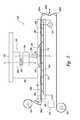
- FIG. 2is a partially schematic illustration of an apparatus for carrying out processes in accordance with embodiments of the invention.
- FIG. 3is a partially schematic, isometric view of a portion of the apparatus shown in FIG. 2 in accordance with an embodiment of the invention.
- FIG. 4is a partially schematic, side elevation view of an apparatus for processing a microelectronic substrate in accordance with another embodiment of the invention.
- FIG. 5schematically illustrates a waveform for electrolytically processing a microelectronic substrate in accordance with another embodiment of the invention.
- FIG. 1Ais a partially schematic illustration of a microelectronic substrate 110 positioned for processing in accordance with an embodiment of the invention.
- the microelectronic substrate 110includes a substrate material 111 , such as borophosphosilicate glass (BPSG), and in other embodiments, the microelectronic substrate 110 can include other substrate materials 111 , such as undoped silicon dioxide.
- BPSGborophosphosilicate glass
- one or more apertures 112can be formed in a substrate material plane 113 of the substrate material 111 , using conventional techniques such as patterned etching.
- the apertures 112have a relatively high aspect ratio (i.e., depth-to-width ratio).
- the apertures 112can have an aspect ratio of about 4:1 or more, and in other embodiments, the apertures 112 can have other aspect ratios.
- an underlayer 114(such as tantalum or tantalum oxide) can be disposed on the substrate material plane 113 and adjacent to the walls of the apertures 112 .
- the underlayer 114can be disposed on the microelectronic substrate 110 using conventional techniques, such as physical vapor deposition (PVD) or chemical vapor deposition (CVD).
- PVDphysical vapor deposition
- CVDchemical vapor deposition
- the underlayer 114can form a barrier layer and in other embodiments, the underlayer 114 can perform other functions, such as promoting adhesion of subsequently deposited materials onto the walls of the apertures 112 .
- a layer of conductive material 115is then disposed on the underlayer 114 .
- the conductive material 115can include platinum or platinum alloys, and in other embodiments, the conductive material 115 can include other electrically conductive constituents, such as rhodium, ruthenium, copper or alloys of these materials. Platinum may be particularly suitable for apertures 112 having high aspect ratios, such as aspect ratios of approximately 4:1 or more.
- a fill material 117is then disposed on the conductive material 115 .
- the fill material 117includes subplane portions 118 (positioned beneath the substrate material plane 113 in the apertures 112 ) and a first external portion 119 that extends outwardly away from the substrate material plane 113 , external to the apertures 112 .
- the first external portion 119is disposed on a second external portion 120 defined by the part of the conductive material 115 located external to the apertures 112 and beyond the substrate material plane 113 .
- the fill material 117can include a relatively hard, generally nonconductive substance, such as phosphosilicate glass (PSG).
- the fill material 117can include PSG having 6% phosphorous.
- the fill material 117can include other relatively hard PSG or non-PSG materials, such as spin-on glass (SOG).
- the fill material 117has a hardness greater than that of a typical photoresist material. Accordingly, in one particular embodiment, the fill material 117 can have a hardness of about 0.04 GPa or higher. In one aspect of this embodiment, the hardness is calculated by driving an indenter with a known geometry into the material and measuring the normal applied force as a function of displacement.
- the hardnessis calculated in accordance with other methods.
- the fill material 117includes 6% phosphorous PSG
- the fill material 117can have a hardness of about 6.5 GPa or higher.
- the relatively hard composition of the fill material 117can resist penetration from particles of the conductive material 115 , as described in greater detail below.
- the first external portion 119 of the fill material 117can be removed (as shown in FIG. 1B ) so that the remaining fill material 117 is flush with the conductive material 115 .
- conventional CMP techniques and slurriesare used to remove the first projection 119 . Apparatuses for removing the first projection 119 are described in greater detail below with reference to FIGS. 2-5 .
- a portion of the remaining fill material 117can be recessed relative to the adjacent conductive material 115 prior to removing the adjacent conductive material 115 .
- the remaining fill material 117can project by distance D 2 (less than D 1 ) from the substrate material plane 113 .
- D 1is approximately 1,000 ⁇
- D 2can be from about 200 ⁇ to about 500 ⁇ .
- the relative values of D 1 and D 2can be different, so long as D 2 is less than D 1 .
- the recess distance(e.g., D 1 minus D 2 ) can be from about 50% to about 80% of D 1 .
- selective etch techniquescan be used to selectively recess the fill material 117 relative to the adjacent second external portion 120 of the conductive material 115 . The second external portion 120 is then removed, as described below.
- FIG. 1Dis a schematic illustration of the microelectronic substrate 110 after the second external portion 120 ( FIG. 1C ) of the conductive material 115 has been removed.
- the second external portion 120can be removed using electrochemical-mechanical polishing (ECMP) techniques and an apparatus generally similar to that described in greater detail below with reference to FIGS. 2-5 .
- ECMPelectrochemical-mechanical polishing
- the removal of the conductive material 115is halted upon exposing the underlayer 114 .
- the conductive material 115is removed more rapidly than is the fill material 117 , so that projections 122 of the fill material 117 extend outwardly from the substrate material plane 113 at the end of this phase of processing.
- the conductive material 115is removed electrolytically, as well as by chemical and/or mechanical action, whereas the generally nonconductive fill material 117 is removed without electrolytic action.
- the projections 122 of the fill material 117are removed in a subsequent step.
- One aspect of an embodiment of the process described above with reference to FIGS. 1C and 1Dis that the fill material 117 is recessed relative to the adjacent conductive material 115 by a selected distance prior to removing the adjacent conductive material 115 .
- One advantage of this processis that recessing the fill material 117 can reduce the likelihood for forming residual deposits of conductive material 115 around the apertures 112 . For example, if the fill material 117 is flush with the second projection 120 (as indicated by distance D 0 in FIG.
- the resulting large mass of fill material 117 extending away from the substrate material plane 113can “shield” the adjacent conductive material 115 and reduce the effectiveness of the ECMP process for removing the conductive material 115 . Accordingly, the process can leave residual deposits 115 a of the conductive material 115 around the apertures 112 , as shown in dashed lines in FIG. 1D . These deposits, if not removed, can cause short-circuits with adjacent structures, and/or can adversely affect subsequent processing steps.
- the fill material 117may not adequately support the conducive material 115 within the apertures 112 during the ECMP and CMP processes, causing the conductive material 115 to shear out of the apertures 112 during processing.
- each container 130includes a volume of fill material 117 surrounded by a layer of conductive material 115 , which is in turn surrounded by the underlayer 114 . At this point, each container 130 is electrically isolated and shielded from the surrounding structures in the microelectronic substrate 110 .
- further featurescan next be disposed in the containers 130 to form structures 121 such as capacitors.
- the featurescan be disposed in the containers 130 using conventional techniques (such as selective etching and deposition) and are electrically coupled to each other and/or to external contacts with a network of vias and/or lines, also formed with conventional techniques, such as damascene techniques.
- the remaining fill material 117 within the apertures 112is removed.
- a film 118formed from a material such as tantalum pentoxide, is then disposed in the apertures 112 , and a conductive electrode 119 is disposed adjacent to the film 118 to form the capacitor.
- the foregoing techniquescan be used to form other features in the microelectronic substrate 110 , such as trenches and/or conductive lines.
- portions of the microelectronic substrate 110can then be diced from the larger wafer of which they are a part for encapsulation and incorporation in electronic devices.
- FIGS. 2-5schematically illustrate apparatuses for processing the microelectronic substrate 110 in a manner generally similar to that described above with reference to FIGS. 1A-1F .
- FIG. 2schematically illustrates an apparatus 260 chemically-mechanically and/or electrochemically-mechanically polishing the microelectronic substrate 110 in accordance with an embodiment of the invention.
- the apparatus 260has a support table 280 with a top-panel 281 at a workstation where an operative portion “W” of a polishing pad 283 is positioned.
- the top-panel 281is generally a rigid plate to provide a flat, solid surface to which a particular section of the polishing pad 283 may be secured during polishing.
- the apparatus 260can also have a plurality of rollers to guide, position and hold the polishing pad 283 over the top-panel 281 .
- the rollerscan include a supply roller 287 , first and second idler rollers 284 a and 284 b , first and second guide rollers 285 a and 285 b , and a take-up roller 286 .
- the supply roller 287carries an unused or preoperative portion of the polishing pad 283
- the take-up roller 286carries a used or postoperative portion of the polishing pad 283 .
- the first idler roller 284 a and the first guide roller 285 acan stretch the polishing pad 283 over the top-panel 281 to hold the polishing pad 283 stationary during operation.
- a motor(not shown) drives at least one of the supply roller 287 the take-up roller 286 to sequentially advance the polishing pad 283 across the top-panel 281 . Accordingly, clean preoperative sections of the polishing pad 283 may be quickly substituted for used sections to provide a consistent surface for polishing and/or cleaning the microelectronic substrate 110 .
- the apparatus 260can also have a carrier assembly 290 that controls and protects the microelectronic substrate 110 during polishing.
- the carrier assembly 290can include a substrate holder 292 to pick up, hold and release the substrate 110 at appropriate stages of the polishing process.
- the carrier assembly 290can also have a support gantry 294 carrying a drive assembly 295 that can translate along the gantry 294 .
- the drive assembly 295can have an actuator 296 , a drive shaft 297 coupled to the actuator 296 , and an arm 298 projecting from the drive shaft 297 .
- the arm 298carries the substrate holder 292 via a terminal shaft 299 such that the drive assembly 295 orbits the substrate holder 292 about an axis E-E (as indicated by arrow “R 1 ”).
- the terminal shaft 299may also rotate the substrate holder 292 about its central axis F-F (as indicated by arrow “R 2 ”).
- the polishing pad 283 and a polishing liquid 289define a polishing medium 282 that mechanically and/or chemically-mechanically removes material from the surface of the microelectronic substrate 110 .
- the polishing pad 283 used in the apparatus 260can be a fixed-abrasive polishing pad in which abrasive particles are fixedly bonded to a suspension medium. Accordingly, the polishing solution 289 can be a “clean solution” without abrasive particles because the abrasive particles are fixedly distributed across a polishing surface 288 of the polishing pad 283 .
- the polishing pad 283may be a nonabrasive pad without abrasive particles
- the polishing solution 289can be a slurry with abrasive particles and chemicals to remove material from the microelectronic substrate 110 .
- the carrier assembly 290presses the microelectronic substrate 110 against the polishing surface 288 of the polishing pad 283 in the presence of the polishing solution 289 .
- the drive assembly 295then orbits the substrate holder 292 about the axis E-E and optionally rotates the substrate holder 292 about the axis F-F to translate the substrate 110 across the polishing surface 288 .
- the abrasive particles and/or the chemicals in the polishing medium 282remove material from the surface of the microelectronic substrate 110 in a chemical and/or chemical-mechanical polishing process.
- the polishing solution 289can include an electrolyte for ECMP processing.
- the apparatus 260can include an electrolyte supply vessel 230 that delivers an electrolyte separately to the polishing surface 288 of the polishing pad 283 with a conduit 237 , as described in greater detail below with reference to FIG. 3 .
- the apparatus 260can further include a current supply 221 coupled to electrodes positioned proximate to the polishing pad 283 . Accordingly, the apparatus 260 can electrolytically remove material from the microelectronic substrate 110 .
- FIG. 3is a partially exploded, partially schematic isometric view of a portion of the apparatus 260 described above with reference to FIG. 2 .
- the top-panel 281houses a plurality of electrode pairs 370 , each of which includes a first electrode 340 a and a second electrode 340 b .
- the first electrodes 340 aare coupled to a first lead 348 a and the second electrodes 340 b are coupled to a second lead 348 b .
- the first and second leads 348 a and 348 bare coupled to the current supply 241 ( FIG. 2 ).
- the first electrodes 340 acan be separated from the second electrodes 340 b by an electrode dielectric layer 349 a that includes TeflonTM or another suitable dielectric material.
- the electrode dielectric layer 349 acan accordingly control the volume and dielectric constant of the region between the first and second electrodes 340 a and 340 b to control the electrical coupling between the electrodes.
- the electrodes 340 a and 340 bcan be electrically coupled to the microelectronic substrate 110 ( FIG. 2 ) by the polishing pad 283 .
- the polishing pad 283is saturated with an electrolyte 331 supplied by the supply conduits 337 through apertures 338 in the top-panel 281 just beneath the polishing pad 283 .
- the electrodes 320 a and 320 bare selected to be compatible with the electrolyte 331 .
- the electrolyte 331can be supplied to the polishing pad 283 from above (for example, by disposing the electrolyte 331 in the polishing liquid 289 , rather than by directing the electrolyte upwardly through the polishing pad 283 ).
- the apparatus 260can include a pad dielectric layer 349 b ( FIG. 2 ) positioned between the polishing pad 283 and the electrodes 340 a and 340 b .
- the electrodes 340 a and 340 bare isolated from physical contact with the electrolyte 331 and can accordingly be selected from materials that are not necessarily compatible with the electrolyte 331 .
- FIG. 4is an isometric view of a portion of an apparatus 460 having electrodes 440 (shown as a first electrode 440 a and a second electrode 440 b ), and a polishing medium 482 arranged in accordance with another embodiment of the invention.
- the polishing medium 482includes polishing pad portions 483 that project beyond the electrodes 440 a and 440 b .
- Each polishing pad portion 483can include a polishing surface 488 and a plurality of flow passages 484 coupled to a fluid source (not shown in FIG. 4 ) with a conduit 437 .
- Each flow passage 484can have an aperture 485 proximate to the polishing surface 488 to provide an electrolyte 431 proximate to an interface between the microelectronic substrate 110 and the polishing surface 488 .
- the pad portions 483can include recesses 487 surrounding each aperture 485 . Accordingly, the electrolyte 431 can proceed outwardly from the flow passages 484 while the microelectronic substrate 110 is positioned directly overhead and remains spaced apart from the electrodes 420 .
- any of the foregoing apparatuses described above with reference to FIGS. 2-4can be used to chemically-mechanically process the microelectronic substrate 110 , and/or electrochemically-mechanically process the microelectronic substrate 110 .
- the apparatusescan provide a varying electrical current that passes from the electrodes, through the conductive material of the microelectronic substrate 110 , via the electrolytic fluid without contacting the electrodes with the microelectronic substrate 110 .
- the apparatuscan generate a high-frequency wave 504 and can superimpose a low-frequency wave 502 on the high-frequency wave 504 .
- the high-frequency wave 504can include a series of positive or negative voltage spikes contained within a square wave envelope defined by the low-frequency wave 502 .
- Each spike of the high-frequency wave 504can have a relatively steep rise-time slope to transfer charge through the dielectric material to the electrolyte and a more gradual fall-time slope.
- the fall-time slopecan define a straight line, as indicated by high-frequency wave 504 , or a curved line, as indicated by high-frequency wave 504 a .
- the high-frequency wave 504 and the low-frequency wave 502can have other shapes depending, for example, on the particular characteristics of the dielectric material and the electrolyte, the characteristics of the microelectronic substrate 110 , and/or the target rate at which conductive material is to be removed from the microelectronic substrate 110 .
Landscapes
- Engineering & Computer Science (AREA)
- Microelectronics & Electronic Packaging (AREA)
- Condensed Matter Physics & Semiconductors (AREA)
- General Physics & Mathematics (AREA)
- Manufacturing & Machinery (AREA)
- Computer Hardware Design (AREA)
- Physics & Mathematics (AREA)
- Power Engineering (AREA)
- Chemical & Material Sciences (AREA)
- Chemical Kinetics & Catalysis (AREA)
- Electrochemistry (AREA)
- Internal Circuitry In Semiconductor Integrated Circuit Devices (AREA)
- Mechanical Treatment Of Semiconductor (AREA)
- Weting (AREA)
Abstract
Description
- This application is a divisional of U.S. application Ser. No. 11/413,256 filed Apr. 28, 2006, which is a divisional of U.S. application Ser. No. 10/230,628 filed Aug. 29, 2002, now U.S. Pat. No. 7,078,308, both of which are incorporated herein by reference.
- This application is related to the following U.S. patent applications, all of which are incorporated herein by reference: U.S. Ser. No. 09/651,779 filed Aug. 30, 2000, now U.S. Pat. No. 7,074,113; U.S. Ser. No. 09/888,084 filed Jun. 21, 2001, now U.S. Pat. No. 7,112,121; U.S. Ser. No. 09/887,767 filed Jun. 21, 2001, now U.S. Pat. No. 7,094,131; U.S. Ser. No. 09/888,002 filed Jun. 21, 2001, now U.S. Pat. No. 7,160,176; U.S. Ser. No. 10/230,970 filed Aug. 29, 2002, now U.S. Pat. No. 7,220,166; U.S. Ser. No. 10/230,972 filed Aug. 29, 2002, now U.S. Pat. No. 7,134,934; U.S. Ser. No. 10/230,973 filed Aug. 29, 2002, now U.S. Pat. No. 7,153,195; U.S. Ser. No. 10/230,463 filed Aug. 29, 2002, now U.S. Pat. No. 7,192,335; and U.S. Ser. No. 11/413,286 filed Apr. 28, 2006, now abandoned.
- The present invention relates generally to methods and apparatuses for removing adjacent conductive and nonconductive materials of a microelectronic substrate.
- Microelectronic substrates and substrate assemblies typically include a semiconductor material having features, such as memory cells, that are linked with conductive lines. The conductive lines can be formed by first forming trenches or other recesses in the semiconductor material and then overlaying a conductive material (such as a metal) in the trenches. The conductive material is then selectively removed to leave conductive lines extending from one feature in the semiconductor material to another.
- One technique for forming microelectronic features, such as capacitors, is to dispose the features in isolated containers within the microelectronic substrate. One typical process includes forming an aperture in a substrate material (such as borophosphosilicate glass or BPSG), coating the microelectronic substrate (including the walls of the aperture) first with a barrier layer and then with a conductive layer, and then overfilling the aperture with a generally nonconductive material, such as a photoresist material. The excess photoresist material, conductive layer material, and barrier layer material located external to the aperture are then removed using chemical-mechanical planarization or polishing (CMP). The capacitor is then disposed within the photoresist material in the aperture and coupled to other features of the microelectronic substrate with an overlying network of vias and lines.
- One drawback with the foregoing container technique for forming capacitors is that during the CMP process, small particles of the conductive material removed from the conductive layer can become embedded in the photoresist material within the aperture. The embedded conductive material can cause short circuits and/or other defects in the capacitor that is subsequently formed in the aperture, causing the capacitor to fail.
- The present invention is directed toward methods and apparatuses for removing adjacent conductive and nonconductive materials of a microelectronic substrate. A method in accordance with one aspect of the invention includes forming an aperture in a microelectronic substrate material, disposing a conductive material in the aperture proximate to a wall of the aperture, and disposing a fill material in the aperture proximate to the conductive material. In one aspect of this embodiment, the fill material has a hardness of about 0.04 GPa or higher, and in another aspect of the invention, the fill material has a hardness of about 6.5 GPa or higher. For example, the fill material can include a phosphosilicate glass or a spin-on glass. A microelectronic feature, such as an electrode, can then be disposed in the aperture.
- A method in accordance with another aspect of the invention includes providing a microelectronic substrate having a substrate material defining a substrate material plane, a conductive material proximate to the substrate material, and a generally nonconductive material proximate to the conductive material. The conductive material is accordingly positioned between the substrate material and the generally nonconductive material. A portion of the generally nonconductive material includes a first external portion projecting beyond the substrate material plane, and a portion of the conductive material includes a second external portion projecting beyond the substrate material plane. At least part of the first external portion extending beyond the second external portion is removed, and the fill material is recessed inwardly toward the substrate material plane. At least part of the second external portion is also removed. For example, the first external portion can be removed via chemical-mechanical polishing, and the second external portion can be removed via electrochemical-mechanical polishing. In a further aspect of the invention, the first external portion can be recessed until it extends outwardly from the substrate material plane by distance from about 200 Å to about 500 Å.
FIGS. 1A-1F schematically illustrate a process for forming features in a microelectronic substrate in accordance with an embodiment of the invention.FIG. 2 is a partially schematic illustration of an apparatus for carrying out processes in accordance with embodiments of the invention.FIG. 3 is a partially schematic, isometric view of a portion of the apparatus shown inFIG. 2 in accordance with an embodiment of the invention.FIG. 4 is a partially schematic, side elevation view of an apparatus for processing a microelectronic substrate in accordance with another embodiment of the invention.FIG. 5 schematically illustrates a waveform for electrolytically processing a microelectronic substrate in accordance with another embodiment of the invention.- The present disclosure describes methods and apparatuses for processing microelectronic substrates. Many specific details of certain embodiments of the invention are set forth in the following description and in
FIGS. 1A-5 to provide a thorough understanding of these embodiments. One skilled in the art, however, will understand that the present invention may have additional embodiments and that the invention may be practiced without several of the details described below. FIG. 1A is a partially schematic illustration of amicroelectronic substrate 110 positioned for processing in accordance with an embodiment of the invention. In one aspect of this embodiment, themicroelectronic substrate 110 includes asubstrate material 111, such as borophosphosilicate glass (BPSG), and in other embodiments, themicroelectronic substrate 110 can includeother substrate materials 111, such as undoped silicon dioxide. In any of these embodiments, one or more apertures112 (two of which are shown inFIG. 1A ) can be formed in asubstrate material plane 113 of thesubstrate material 111, using conventional techniques such as patterned etching. In one embodiment, theapertures 112 have a relatively high aspect ratio (i.e., depth-to-width ratio). For example, in one particular embodiment, theapertures 112 can have an aspect ratio of about 4:1 or more, and in other embodiments, theapertures 112 can have other aspect ratios. In any of these embodiments, an underlayer114 (such as tantalum or tantalum oxide) can be disposed on thesubstrate material plane 113 and adjacent to the walls of theapertures 112. Theunderlayer 114 can be disposed on themicroelectronic substrate 110 using conventional techniques, such as physical vapor deposition (PVD) or chemical vapor deposition (CVD). In one aspect of this embodiment, theunderlayer 114 can form a barrier layer and in other embodiments, theunderlayer 114 can perform other functions, such as promoting adhesion of subsequently deposited materials onto the walls of theapertures 112.- A layer of
conductive material 115 is then disposed on theunderlayer 114. In one embodiment, theconductive material 115 can include platinum or platinum alloys, and in other embodiments, theconductive material 115 can include other electrically conductive constituents, such as rhodium, ruthenium, copper or alloys of these materials. Platinum may be particularly suitable forapertures 112 having high aspect ratios, such as aspect ratios of approximately 4:1 or more. - A
fill material 117 is then disposed on theconductive material 115. Thefill material 117 includes subplane portions118 (positioned beneath thesubstrate material plane 113 in the apertures112) and a firstexternal portion 119 that extends outwardly away from thesubstrate material plane 113, external to theapertures 112. The firstexternal portion 119 is disposed on a secondexternal portion 120 defined by the part of theconductive material 115 located external to theapertures 112 and beyond thesubstrate material plane 113. - In one embodiment, the
fill material 117 can include a relatively hard, generally nonconductive substance, such as phosphosilicate glass (PSG). In a specific aspect of this embodiment, thefill material 117 can include PSG having 6% phosphorous. In other embodiments, thefill material 117 can include other relatively hard PSG or non-PSG materials, such as spin-on glass (SOG). In any of these embodiments, thefill material 117 has a hardness greater than that of a typical photoresist material. Accordingly, in one particular embodiment, thefill material 117 can have a hardness of about 0.04 GPa or higher. In one aspect of this embodiment, the hardness is calculated by driving an indenter with a known geometry into the material and measuring the normal applied force as a function of displacement. In other embodiments, the hardness is calculated in accordance with other methods. In a particular embodiment in which thefill material 117 includes 6% phosphorous PSG, thefill material 117 can have a hardness of about 6.5 GPa or higher. In any of these embodiments, the relatively hard composition of thefill material 117 can resist penetration from particles of theconductive material 115, as described in greater detail below. - The first
external portion 119 of thefill material 117 can be removed (as shown inFIG. 1B ) so that the remainingfill material 117 is flush with theconductive material 115. In one aspect of this embodiment, conventional CMP techniques and slurries are used to remove thefirst projection 119. Apparatuses for removing thefirst projection 119 are described in greater detail below with reference toFIGS. 2-5 . - As shown in
FIG. 1C , a portion of the remainingfill material 117 can be recessed relative to the adjacentconductive material 115 prior to removing the adjacentconductive material 115. For example, when theconductive material 115 projects away from thesubstrate material plane 113 by a distance D1, the remainingfill material 117 can project by distance D2(less than D1) from thesubstrate material plane 113. In one particular embodiment, where D1is approximately 1,000 Å, D2can be from about 200 Å to about 500 Å. In other embodiments, the relative values of D1and D2can be different, so long as D2is less than D1. For example, the recess distance (e.g., D1minus D2) can be from about 50% to about 80% of D1. In any of these embodiments, selective etch techniques can be used to selectively recess thefill material 117 relative to the adjacent secondexternal portion 120 of theconductive material 115. The secondexternal portion 120 is then removed, as described below. FIG. 1D is a schematic illustration of themicroelectronic substrate 110 after the second external portion120 (FIG. 1C ) of theconductive material 115 has been removed. The secondexternal portion 120 can be removed using electrochemical-mechanical polishing (ECMP) techniques and an apparatus generally similar to that described in greater detail below with reference toFIGS. 2-5 . In one aspect of this embodiment, the removal of theconductive material 115 is halted upon exposing theunderlayer 114. In a further aspect of this embodiment, theconductive material 115 is removed more rapidly than is thefill material 117, so thatprojections 122 of thefill material 117 extend outwardly from thesubstrate material plane 113 at the end of this phase of processing. For example, during ECMP processing, theconductive material 115 is removed electrolytically, as well as by chemical and/or mechanical action, whereas the generallynonconductive fill material 117 is removed without electrolytic action. As will be described in greater detail below with reference toFIG. 1E , theprojections 122 of thefill material 117 are removed in a subsequent step.- One aspect of an embodiment of the process described above with reference to
FIGS. 1C and 1D is that thefill material 117 is recessed relative to the adjacentconductive material 115 by a selected distance prior to removing the adjacentconductive material 115. One advantage of this process is that recessing thefill material 117 can reduce the likelihood for forming residual deposits ofconductive material 115 around theapertures 112. For example, if thefill material 117 is flush with the second projection120 (as indicated by distance D0inFIG. 1C ) when theconductive material 115 is removed, the resulting large mass offill material 117 extending away from thesubstrate material plane 113 can “shield” the adjacentconductive material 115 and reduce the effectiveness of the ECMP process for removing theconductive material 115. Accordingly, the process can leaveresidual deposits 115aof theconductive material 115 around theapertures 112, as shown in dashed lines inFIG. 1D . These deposits, if not removed, can cause short-circuits with adjacent structures, and/or can adversely affect subsequent processing steps. Conversely, if thefill material 117 is recessed substantially lower than the distance D2, thefill material 117 may not adequately support theconducive material 115 within theapertures 112 during the ECMP and CMP processes, causing theconductive material 115 to shear out of theapertures 112 during processing. - The
projections 122 of thefill material 117, along with the portions of theunderlayer 114 and theconductive material 115 extending out of theapertures 112, are then removed to form thecontainers 130, as shown inFIG. 1E . Accordingly, eachcontainer 130 includes a volume offill material 117 surrounded by a layer ofconductive material 115, which is in turn surrounded by theunderlayer 114. At this point, eachcontainer 130 is electrically isolated and shielded from the surrounding structures in themicroelectronic substrate 110. - As shown in
FIG. 1F , further features (such as electrodes) can next be disposed in thecontainers 130 to formstructures 121 such as capacitors. The features can be disposed in thecontainers 130 using conventional techniques (such as selective etching and deposition) and are electrically coupled to each other and/or to external contacts with a network of vias and/or lines, also formed with conventional techniques, such as damascene techniques. For example, in one embodiment, the remainingfill material 117 within theapertures 112 is removed. Afilm 118, formed from a material such as tantalum pentoxide, is then disposed in theapertures 112, and aconductive electrode 119 is disposed adjacent to thefilm 118 to form the capacitor. In other embodiments, the foregoing techniques can be used to form other features in themicroelectronic substrate 110, such as trenches and/or conductive lines. In any of these embodiments, portions of themicroelectronic substrate 110 can then be diced from the larger wafer of which they are a part for encapsulation and incorporation in electronic devices. FIGS. 2-5 schematically illustrate apparatuses for processing themicroelectronic substrate 110 in a manner generally similar to that described above with reference toFIGS. 1A-1F . For example,FIG. 2 schematically illustrates anapparatus 260 chemically-mechanically and/or electrochemically-mechanically polishing themicroelectronic substrate 110 in accordance with an embodiment of the invention. In one aspect of this embodiment, theapparatus 260 has a support table280 with a top-panel 281 at a workstation where an operative portion “W” of apolishing pad 283 is positioned. The top-panel 281 is generally a rigid plate to provide a flat, solid surface to which a particular section of thepolishing pad 283 may be secured during polishing.- The
apparatus 260 can also have a plurality of rollers to guide, position and hold thepolishing pad 283 over the top-panel 281. The rollers can include asupply roller 287, first and secondidler rollers second guide rollers roller 286. Thesupply roller 287 carries an unused or preoperative portion of thepolishing pad 283, and the take-uproller 286 carries a used or postoperative portion of thepolishing pad 283. Additionally, thefirst idler roller 284aand thefirst guide roller 285acan stretch thepolishing pad 283 over the top-panel 281 to hold thepolishing pad 283 stationary during operation. A motor (not shown) drives at least one of thesupply roller 287 the take-uproller 286 to sequentially advance thepolishing pad 283 across the top-panel 281. Accordingly, clean preoperative sections of thepolishing pad 283 may be quickly substituted for used sections to provide a consistent surface for polishing and/or cleaning themicroelectronic substrate 110. - The
apparatus 260 can also have acarrier assembly 290 that controls and protects themicroelectronic substrate 110 during polishing. Thecarrier assembly 290 can include a substrate holder292 to pick up, hold and release thesubstrate 110 at appropriate stages of the polishing process. Thecarrier assembly 290 can also have asupport gantry 294 carrying adrive assembly 295 that can translate along thegantry 294. Thedrive assembly 295 can have anactuator 296, adrive shaft 297 coupled to theactuator 296, and anarm 298 projecting from thedrive shaft 297. Thearm 298 carries the substrate holder292 via a terminal shaft299 such that thedrive assembly 295 orbits the substrate holder292 about an axis E-E (as indicated by arrow “R1”). The terminal shaft299 may also rotate the substrate holder292 about its central axis F-F (as indicated by arrow “R2”). - The
polishing pad 283 and a polishing liquid289 define a polishing medium282 that mechanically and/or chemically-mechanically removes material from the surface of themicroelectronic substrate 110. Thepolishing pad 283 used in theapparatus 260 can be a fixed-abrasive polishing pad in which abrasive particles are fixedly bonded to a suspension medium. Accordingly, thepolishing solution 289 can be a “clean solution” without abrasive particles because the abrasive particles are fixedly distributed across a polishingsurface 288 of thepolishing pad 283. In other applications, thepolishing pad 283 may be a nonabrasive pad without abrasive particles, and thepolishing solution 289 can be a slurry with abrasive particles and chemicals to remove material from themicroelectronic substrate 110. To polish themicroelectronic substrate 110 with theapparatus 260, thecarrier assembly 290 presses themicroelectronic substrate 110 against the polishingsurface 288 of thepolishing pad 283 in the presence of thepolishing solution 289. Thedrive assembly 295 then orbits the substrate holder292 about the axis E-E and optionally rotates the substrate holder292 about the axis F-F to translate thesubstrate 110 across the polishingsurface 288. As a result, the abrasive particles and/or the chemicals in the polishing medium282 remove material from the surface of themicroelectronic substrate 110 in a chemical and/or chemical-mechanical polishing process. - In a further aspect of this embodiment, the
polishing solution 289 can include an electrolyte for ECMP processing. In another embodiment, theapparatus 260 can include anelectrolyte supply vessel 230 that delivers an electrolyte separately to the polishingsurface 288 of thepolishing pad 283 with aconduit 237, as described in greater detail below with reference toFIG. 3 . In either embodiment, theapparatus 260 can further include acurrent supply 221 coupled to electrodes positioned proximate to thepolishing pad 283. Accordingly, theapparatus 260 can electrolytically remove material from themicroelectronic substrate 110. FIG. 3 is a partially exploded, partially schematic isometric view of a portion of theapparatus 260 described above with reference toFIG. 2 . In one aspect of the embodiment shown inFIG. 3 , the top-panel 281 houses a plurality of electrode pairs370, each of which includes afirst electrode 340aand asecond electrode 340b. Thefirst electrodes 340aare coupled to afirst lead 348aand thesecond electrodes 340bare coupled to asecond lead 348b. The first andsecond leads FIG. 2 ). In one aspect of this embodiment, thefirst electrodes 340acan be separated from thesecond electrodes 340bby anelectrode dielectric layer 349athat includes Teflon™ or another suitable dielectric material. Theelectrode dielectric layer 349acan accordingly control the volume and dielectric constant of the region between the first andsecond electrodes - The
electrodes FIG. 2 ) by thepolishing pad 283. In one aspect of this embodiment, thepolishing pad 283 is saturated with anelectrolyte 331 supplied by thesupply conduits 337 throughapertures 338 in the top-panel 281 just beneath thepolishing pad 283. Accordingly, the electrodes320aand320bare selected to be compatible with theelectrolyte 331. In an another arrangement, theelectrolyte 331 can be supplied to thepolishing pad 283 from above (for example, by disposing theelectrolyte 331 in the polishingliquid 289, rather than by directing the electrolyte upwardly through the polishing pad283). Accordingly, theapparatus 260 can include apad dielectric layer 349b(FIG. 2 ) positioned between thepolishing pad 283 and theelectrodes pad dielectric layer 349bis in place, theelectrodes electrolyte 331 and can accordingly be selected from materials that are not necessarily compatible with theelectrolyte 331. FIG. 4 is an isometric view of a portion of anapparatus 460 having electrodes440 (shown as afirst electrode 440aand asecond electrode 440b), and a polishing medium482 arranged in accordance with another embodiment of the invention. In one aspect of this embodiment, the polishingmedium 482 includes polishingpad portions 483 that project beyond theelectrodes polishing pad portion 483 can include a polishingsurface 488 and a plurality offlow passages 484 coupled to a fluid source (not shown inFIG. 4 ) with aconduit 437. Eachflow passage 484 can have anaperture 485 proximate to the polishingsurface 488 to provide anelectrolyte 431 proximate to an interface between themicroelectronic substrate 110 and the polishingsurface 488. In one aspect of this embodiment, thepad portions 483 can include recesses487 surrounding eachaperture 485. Accordingly, theelectrolyte 431 can proceed outwardly from theflow passages 484 while themicroelectronic substrate 110 is positioned directly overhead and remains spaced apart from the electrodes420.- Any of the foregoing apparatuses described above with reference to
FIGS. 2-4 can be used to chemically-mechanically process themicroelectronic substrate 110, and/or electrochemically-mechanically process themicroelectronic substrate 110. When the apparatuses are used to electrochemically-mechanically process themicroelectronic substrate 110, they can provide a varying electrical current that passes from the electrodes, through the conductive material of themicroelectronic substrate 110, via the electrolytic fluid without contacting the electrodes with themicroelectronic substrate 110. For example, as shown inFIG. 5 , the apparatus can generate a high-frequency wave 504 and can superimpose a low-frequency wave 502 on the high-frequency wave 504. In one aspect of this embodiment, the high-frequency wave 504 can include a series of positive or negative voltage spikes contained within a square wave envelope defined by the low-frequency wave 502. Each spike of the high-frequency wave 504 can have a relatively steep rise-time slope to transfer charge through the dielectric material to the electrolyte and a more gradual fall-time slope. The fall-time slope can define a straight line, as indicated by high-frequency wave 504, or a curved line, as indicated by high-frequency wave 504a. In other embodiments, the high-frequency wave 504 and the low-frequency wave 502 can have other shapes depending, for example, on the particular characteristics of the dielectric material and the electrolyte, the characteristics of themicroelectronic substrate 110, and/or the target rate at which conductive material is to be removed from themicroelectronic substrate 110. - From the foregoing, it will be appreciated that specific embodiments of the invention have been described herein for purposes of illustration, but that various modifications may be made without deviating from the spirit and scope of the invention. For example, many of the structures and processes described above in the content of microelectronic containers can also be applied to other microelectronic features. Accordingly, the invention is not limited except as by the appended claims.
Claims (20)
Priority Applications (1)
| Application Number | Priority Date | Filing Date | Title |
|---|---|---|---|
| US12/731,049US8048756B2 (en) | 2002-08-29 | 2010-03-24 | Method for removing metal layers formed outside an aperture of a BPSG layer utilizing multiple etching processes including electrochemical-mechanical polishing |
Applications Claiming Priority (3)
| Application Number | Priority Date | Filing Date | Title |
|---|---|---|---|
| US10/230,628US7078308B2 (en) | 2002-08-29 | 2002-08-29 | Method and apparatus for removing adjacent conductive and nonconductive materials of a microelectronic substrate |
| US11/413,256US7700436B2 (en) | 2002-08-29 | 2006-04-28 | Method for forming a microelectronic structure having a conductive material and a fill material with a hardness of 0.04 GPA or higher within an aperture |
| US12/731,049US8048756B2 (en) | 2002-08-29 | 2010-03-24 | Method for removing metal layers formed outside an aperture of a BPSG layer utilizing multiple etching processes including electrochemical-mechanical polishing |
Related Parent Applications (1)
| Application Number | Title | Priority Date | Filing Date |
|---|---|---|---|
| US11/413,256DivisionUS7700436B2 (en) | 2002-08-29 | 2006-04-28 | Method for forming a microelectronic structure having a conductive material and a fill material with a hardness of 0.04 GPA or higher within an aperture |
Publications (2)
| Publication Number | Publication Date |
|---|---|
| US20100176083A1true US20100176083A1 (en) | 2010-07-15 |
| US8048756B2 US8048756B2 (en) | 2011-11-01 |
Family
ID=31976535
Family Applications (4)
| Application Number | Title | Priority Date | Filing Date |
|---|---|---|---|
| US10/230,628Expired - LifetimeUS7078308B2 (en) | 2000-08-30 | 2002-08-29 | Method and apparatus for removing adjacent conductive and nonconductive materials of a microelectronic substrate |
| US11/413,286AbandonedUS20060208322A1 (en) | 2002-08-29 | 2006-04-28 | Method and apparatus for removing adjacent conductive and non-conductive materials of a microelectronic substrate |
| US11/413,256Expired - LifetimeUS7700436B2 (en) | 2002-08-29 | 2006-04-28 | Method for forming a microelectronic structure having a conductive material and a fill material with a hardness of 0.04 GPA or higher within an aperture |
| US12/731,049Expired - Fee RelatedUS8048756B2 (en) | 2002-08-29 | 2010-03-24 | Method for removing metal layers formed outside an aperture of a BPSG layer utilizing multiple etching processes including electrochemical-mechanical polishing |
Family Applications Before (3)
| Application Number | Title | Priority Date | Filing Date |
|---|---|---|---|
| US10/230,628Expired - LifetimeUS7078308B2 (en) | 2000-08-30 | 2002-08-29 | Method and apparatus for removing adjacent conductive and nonconductive materials of a microelectronic substrate |
| US11/413,286AbandonedUS20060208322A1 (en) | 2002-08-29 | 2006-04-28 | Method and apparatus for removing adjacent conductive and non-conductive materials of a microelectronic substrate |
| US11/413,256Expired - LifetimeUS7700436B2 (en) | 2002-08-29 | 2006-04-28 | Method for forming a microelectronic structure having a conductive material and a fill material with a hardness of 0.04 GPA or higher within an aperture |
Country Status (1)
| Country | Link |
|---|---|
| US (4) | US7078308B2 (en) |
Cited By (1)
| Publication number | Priority date | Publication date | Assignee | Title |
|---|---|---|---|---|
| US9741817B2 (en)* | 2016-01-21 | 2017-08-22 | Tower Semiconductor Ltd. | Method for manufacturing a trench metal insulator metal capacitor |
Families Citing this family (21)
| Publication number | Priority date | Publication date | Assignee | Title |
|---|---|---|---|---|
| US7134934B2 (en)* | 2000-08-30 | 2006-11-14 | Micron Technology, Inc. | Methods and apparatus for electrically detecting characteristics of a microelectronic substrate and/or polishing medium |
| US7129160B2 (en)* | 2002-08-29 | 2006-10-31 | Micron Technology, Inc. | Method for simultaneously removing multiple conductive materials from microelectronic substrates |
| US7112121B2 (en)* | 2000-08-30 | 2006-09-26 | Micron Technology, Inc. | Methods and apparatus for electrical, mechanical and/or chemical removal of conductive material from a microelectronic substrate |
| US7074113B1 (en)* | 2000-08-30 | 2006-07-11 | Micron Technology, Inc. | Methods and apparatus for removing conductive material from a microelectronic substrate |
| US7078308B2 (en)* | 2002-08-29 | 2006-07-18 | Micron Technology, Inc. | Method and apparatus for removing adjacent conductive and nonconductive materials of a microelectronic substrate |
| US7153195B2 (en)* | 2000-08-30 | 2006-12-26 | Micron Technology, Inc. | Methods and apparatus for selectively removing conductive material from a microelectronic substrate |
| US7220166B2 (en)* | 2000-08-30 | 2007-05-22 | Micron Technology, Inc. | Methods and apparatus for electromechanically and/or electrochemically-mechanically removing conductive material from a microelectronic substrate |
| US7160176B2 (en)* | 2000-08-30 | 2007-01-09 | Micron Technology, Inc. | Methods and apparatus for electrically and/or chemically-mechanically removing conductive material from a microelectronic substrate |
| US7112122B2 (en)* | 2003-09-17 | 2006-09-26 | Micron Technology, Inc. | Methods and apparatus for removing conductive material from a microelectronic substrate |
| WO2005069372A1 (en)* | 2003-12-18 | 2005-07-28 | International Business Machines Corporation | Carbon nanotube conductor for trench capacitors |
| US7153777B2 (en)* | 2004-02-20 | 2006-12-26 | Micron Technology, Inc. | Methods and apparatuses for electrochemical-mechanical polishing |
| US20060043534A1 (en)* | 2004-08-26 | 2006-03-02 | Kirby Kyle K | Microfeature dies with porous regions, and associated methods and systems |
| US7566391B2 (en)* | 2004-09-01 | 2009-07-28 | Micron Technology, Inc. | Methods and systems for removing materials from microfeature workpieces with organic and/or non-aqueous electrolytic media |
| US7416975B2 (en)* | 2005-09-21 | 2008-08-26 | Novellus Systems, Inc. | Method of forming contact layers on substrates |
| US7619310B2 (en)* | 2006-11-03 | 2009-11-17 | Infineon Technologies Ag | Semiconductor interconnect and method of making same |
| US8772939B2 (en)* | 2008-08-04 | 2014-07-08 | Micron Technology, Inc. | Polishing systems and methods for removing conductive material from microelectronic substrates |
| US8594216B2 (en) | 2010-08-25 | 2013-11-26 | Qualcomm Incorporated | Beamforming feedback options for MU-MIMO |
| US20120255635A1 (en)* | 2011-04-11 | 2012-10-11 | Applied Materials, Inc. | Method and apparatus for refurbishing gas distribution plate surfaces |
| US8896521B2 (en) | 2012-04-24 | 2014-11-25 | Qualcomm Mems Technologies, Inc. | Metal-insulator-metal capacitors on glass substrates |
| US10115671B2 (en) | 2012-08-03 | 2018-10-30 | Snaptrack, Inc. | Incorporation of passives and fine pitch through via for package on package |
| WO2017091482A1 (en)* | 2015-11-23 | 2017-06-01 | Corning Incorporated | Removal of inorganic coatings from glass substrates |
Citations (95)
| Publication number | Priority date | Publication date | Assignee | Title |
|---|---|---|---|---|
| US2315695A (en)* | 1938-11-23 | 1943-04-06 | Battelle Memorial Institute | Method of polishing metals |
| US2516105A (en)* | 1945-06-20 | 1950-07-25 | Mateosian Edward Der | Electrolytic polishing of metals |
| US3239439A (en)* | 1962-07-09 | 1966-03-08 | Bell Telephone Labor Inc | Electrodeposition of metals |
| US3334210A (en)* | 1964-05-22 | 1967-08-01 | Cincinnati Milling Machine Co | Electro-discharge machining fluid and method |
| US4613417A (en)* | 1984-12-28 | 1986-09-23 | At&T Bell Laboratories | Semiconductor etching process |
| US4839005A (en)* | 1987-05-22 | 1989-06-13 | Kabushiki Kaisha Kobe Seiko Sho | Electrolytic-abrasive polishing method of aluminum surface |
| US5098533A (en)* | 1991-02-06 | 1992-03-24 | International Business Machines Corp. | Electrolytic method for the etch back of encapsulated copper-Invar-copper core structures |
| US5162248A (en)* | 1992-03-13 | 1992-11-10 | Micron Technology, Inc. | Optimized container stacked capacitor DRAM cell utilizing sacrificial oxide deposition and chemical mechanical polishing |
| US5244534A (en)* | 1992-01-24 | 1993-09-14 | Micron Technology, Inc. | Two-step chemical mechanical polishing process for producing flush and protruding tungsten plugs |
| US5300155A (en)* | 1992-12-23 | 1994-04-05 | Micron Semiconductor, Inc. | IC chemical mechanical planarization process incorporating slurry temperature control |
| US5344539A (en)* | 1992-03-30 | 1994-09-06 | Seiko Instruments Inc. | Electrochemical fine processing apparatus |
| US5562529A (en)* | 1992-10-08 | 1996-10-08 | Fujitsu Limited | Apparatus and method for uniformly polishing a wafer |
| US5567300A (en)* | 1994-09-02 | 1996-10-22 | Ibm Corporation | Electrochemical metal removal technique for planarization of surfaces |
| US5575885A (en)* | 1993-12-14 | 1996-11-19 | Kabushiki Kaisha Toshiba | Copper-based metal polishing solution and method for manufacturing semiconductor device |
| US5618381A (en)* | 1992-01-24 | 1997-04-08 | Micron Technology, Inc. | Multiple step method of chemical-mechanical polishing which minimizes dishing |
| US5676587A (en)* | 1995-12-06 | 1997-10-14 | International Business Machines Corporation | Selective polish process for titanium, titanium nitride, tantalum and tantalum nitride |
| US5681423A (en)* | 1996-06-06 | 1997-10-28 | Micron Technology, Inc. | Semiconductor wafer for improved chemical-mechanical polishing over large area features |
| US5780358A (en)* | 1996-04-08 | 1998-07-14 | Chartered Semiconductor Manufacturing Ltd. | Method for chemical-mechanical polish (CMP) planarizing of cooper containing conductor layers |
| US5800248A (en)* | 1996-04-26 | 1998-09-01 | Ontrak Systems Inc. | Control of chemical-mechanical polishing rate across a substrate surface |
| US5807165A (en)* | 1997-03-26 | 1998-09-15 | International Business Machines Corporation | Method of electrochemical mechanical planarization |
| US5840629A (en)* | 1995-12-14 | 1998-11-24 | Sematech, Inc. | Copper chemical mechanical polishing slurry utilizing a chromate oxidant |
| US5843818A (en)* | 1995-12-05 | 1998-12-01 | Samsung Electronics Co., Ltd. | Methods of fabricating ferroelectric capacitors |
| US5846398A (en)* | 1996-08-23 | 1998-12-08 | Sematech, Inc. | CMP slurry measurement and control technique |
| US5888866A (en)* | 1998-04-18 | 1999-03-30 | United Microelectronics Corp. | Method for fabricating capacitors of a dynamic random access memory |
| US5897375A (en)* | 1997-10-20 | 1999-04-27 | Motorola, Inc. | Chemical mechanical polishing (CMP) slurry for copper and method of use in integrated circuit manufacture |
| US5911619A (en)* | 1997-03-26 | 1999-06-15 | International Business Machines Corporation | Apparatus for electrochemical mechanical planarization |
| US5930699A (en)* | 1996-11-12 | 1999-07-27 | Ericsson Inc. | Address retrieval system |
| US5934980A (en)* | 1997-06-09 | 1999-08-10 | Micron Technology, Inc. | Method of chemical mechanical polishing |
| US5952687A (en)* | 1994-09-17 | 1999-09-14 | Kabushiki Kaisha Toshiba | Semiconductor memory device having a trench capacitor with lower electrode inside the trench |
| US5954975A (en)* | 1993-11-03 | 1999-09-21 | Intel Corporation | Slurries for chemical mechanical polishing tungsten films |
| US5954997A (en)* | 1996-12-09 | 1999-09-21 | Cabot Corporation | Chemical mechanical polishing slurry useful for copper substrates |
| US5972792A (en)* | 1996-10-18 | 1999-10-26 | Micron Technology, Inc. | Method for chemical-mechanical planarization of a substrate on a fixed-abrasive polishing pad |
| US5993637A (en)* | 1996-12-06 | 1999-11-30 | Canon Kabushiki Kaisha | Electrode structure, electrolytic etching process and apparatus |
| US6001730A (en)* | 1997-10-20 | 1999-12-14 | Motorola, Inc. | Chemical mechanical polishing (CMP) slurry for polishing copper interconnects which use tantalum-based barrier layers |
| US6007695A (en)* | 1997-09-30 | 1999-12-28 | Candescent Technologies Corporation | Selective removal of material using self-initiated galvanic activity in electrolytic bath |
| US6010964A (en)* | 1997-08-20 | 2000-01-04 | Micron Technology, Inc. | Wafer surface treatment methods and systems using electrocapillarity |
| US6024856A (en)* | 1997-10-10 | 2000-02-15 | Enthone-Omi, Inc. | Copper metallization of silicon wafers using insoluble anodes |
| US6033953A (en)* | 1996-12-27 | 2000-03-07 | Texas Instruments Incorporated | Method for manufacturing dielectric capacitor, dielectric memory device |
| US6039633A (en)* | 1998-10-01 | 2000-03-21 | Micron Technology, Inc. | Method and apparatus for mechanical and chemical-mechanical planarization of microelectronic-device substrate assemblies |
| US6051496A (en)* | 1998-09-17 | 2000-04-18 | Taiwan Semiconductor Manufacturing Company | Use of stop layer for chemical mechanical polishing of CU damascene |
| US6060395A (en)* | 1996-07-17 | 2000-05-09 | Micron Technology, Inc. | Planarization method using a slurry including a dispersant |
| US6060386A (en)* | 1997-08-21 | 2000-05-09 | Micron Technology, Inc. | Method and apparatus for forming features in holes, trenches and other voids in the manufacturing of microelectronic devices |
| US6063306A (en)* | 1998-06-26 | 2000-05-16 | Cabot Corporation | Chemical mechanical polishing slurry useful for copper/tantalum substrate |
| US6066030A (en)* | 1999-03-04 | 2000-05-23 | International Business Machines Corporation | Electroetch and chemical mechanical polishing equipment |
| US6066559A (en)* | 1996-02-02 | 2000-05-23 | Micron Technology, Inc. | Method for forming a semiconductor connection with a top surface having an enlarged recess |
| US6068787A (en)* | 1996-11-26 | 2000-05-30 | Cabot Corporation | Composition and slurry useful for metal CMP |
| US6077412A (en)* | 1997-08-22 | 2000-06-20 | Cutek Research, Inc. | Rotating anode for a wafer processing chamber |
| US6083840A (en)* | 1998-11-25 | 2000-07-04 | Arch Specialty Chemicals, Inc. | Slurry compositions and method for the chemical-mechanical polishing of copper and copper alloys |
| US6100197A (en)* | 1998-10-13 | 2000-08-08 | Nec Corporation | Method of fabricating a semiconductor device |
| US6103636A (en)* | 1997-08-20 | 2000-08-15 | Micron Technology, Inc. | Method and apparatus for selective removal of material from wafer alignment marks |
| US6103628A (en)* | 1998-12-01 | 2000-08-15 | Nutool, Inc. | Reverse linear polisher with loadable housing |
| US6103096A (en)* | 1997-11-12 | 2000-08-15 | International Business Machines Corporation | Apparatus and method for the electrochemical etching of a wafer |
| US6115233A (en)* | 1996-06-28 | 2000-09-05 | Lsi Logic Corporation | Integrated circuit device having a capacitor with the dielectric peripheral region being greater than the dielectric central region |
| US6117781A (en)* | 1999-04-22 | 2000-09-12 | Advanced Micro Devices, Inc. | Optimized trench/via profile for damascene processing |
| US6121152A (en)* | 1998-06-11 | 2000-09-19 | Integrated Process Equipment Corporation | Method and apparatus for planarization of metallized semiconductor wafers using a bipolar electrode assembly |
| US6132586A (en)* | 1998-06-11 | 2000-10-17 | Integrated Process Equipment Corporation | Method and apparatus for non-contact metal plating of semiconductor wafers using a bipolar electrode assembly |
| US6143155A (en)* | 1998-06-11 | 2000-11-07 | Speedfam Ipec Corp. | Method for simultaneous non-contact electrochemical plating and planarizing of semiconductor wafers using a bipiolar electrode assembly |
| US6162681A (en)* | 1998-01-26 | 2000-12-19 | Texas Instruments - Acer Incorporated | DRAM cell with a fork-shaped capacitor |
| US6171467B1 (en)* | 1997-11-25 | 2001-01-09 | The John Hopkins University | Electrochemical-control of abrasive polishing and machining rates |
| US6174425B1 (en)* | 1997-05-14 | 2001-01-16 | Motorola, Inc. | Process for depositing a layer of material over a substrate |
| US6176992B1 (en)* | 1998-11-03 | 2001-01-23 | Nutool, Inc. | Method and apparatus for electro-chemical mechanical deposition |
| US6180947B1 (en)* | 1998-08-07 | 2001-01-30 | Nikon Corporation | Multi-element deflection aberration correction for electron beam lithography |
| US6187651B1 (en)* | 1998-05-07 | 2001-02-13 | Samsung Electronics Co., Ltd. | Methods of forming trench isolation regions using preferred stress relieving layers and techniques to inhibit the occurrence of voids |
| US6190494B1 (en)* | 1998-07-29 | 2001-02-20 | Micron Technology, Inc. | Method and apparatus for electrically endpointing a chemical-mechanical planarization process |
| US6197182B1 (en)* | 1999-07-07 | 2001-03-06 | Technic Inc. | Apparatus and method for plating wafers, substrates and other articles |
| US6196899B1 (en)* | 1999-06-21 | 2001-03-06 | Micron Technology, Inc. | Polishing apparatus |
| US6206756B1 (en)* | 1998-11-10 | 2001-03-27 | Micron Technology, Inc. | Tungsten chemical-mechanical polishing process using a fixed abrasive polishing pad and a tungsten layer chemical-mechanical polishing solution specifically adapted for chemical-mechanical polishing with a fixed abrasive pad |
| US6218309B1 (en)* | 1999-06-30 | 2001-04-17 | Lam Research Corporation | Method of achieving top rounding and uniform etch depths while etching shallow trench isolation features |
| US6250994B1 (en)* | 1998-10-01 | 2001-06-26 | Micron Technology, Inc. | Methods and apparatuses for mechanical and chemical-mechanical planarization of microelectronic-device substrate assemblies on planarizing pads |
| US20010006245A1 (en)* | 1999-12-28 | 2001-07-05 | Takashi Yunogami | Manufacturing method of semiconductor integrated circuit device |
| US6259128B1 (en)* | 1999-04-23 | 2001-07-10 | International Business Machines Corporation | Metal-insulator-metal capacitor for copper damascene process and method of forming the same |
| US6276996B1 (en)* | 1998-11-10 | 2001-08-21 | Micron Technology, Inc. | Copper chemical-mechanical polishing process using a fixed abrasive polishing pad and a copper layer chemical-mechanical polishing solution specifically adapted for chemical-mechanical polishing with a fixed abrasive pad |
| US6280581B1 (en)* | 1998-12-29 | 2001-08-28 | David Cheng | Method and apparatus for electroplating films on semiconductor wafers |
| US6287974B1 (en)* | 1999-06-30 | 2001-09-11 | Lam Research Corporation | Method of achieving top rounding and uniform etch depths while etching shallow trench isolation features |
| US20010025976A1 (en)* | 1998-10-16 | 2001-10-04 | Lee Byoung-Taek | Method for manufacturing a capacitor of a semiconductor device |
| US6299741B1 (en)* | 1999-11-29 | 2001-10-09 | Applied Materials, Inc. | Advanced electrolytic polish (AEP) assisted metal wafer planarization method and apparatus |
| US6303956B1 (en)* | 1999-02-26 | 2001-10-16 | Micron Technology, Inc. | Conductive container structures having a dielectric cap |
| US20010036746A1 (en)* | 2000-03-09 | 2001-11-01 | Shuzo Sato | Methods of producing and polishing semiconductor device and polishing apparatus |
| US20010035354A1 (en)* | 2000-05-12 | 2001-11-01 | Nu Tool Inc. | Method of and apparatus for making electrical contact to wafer surface for full-face electroplating or electropolishing |
| US6313038B1 (en)* | 2000-04-26 | 2001-11-06 | Micron Technology, Inc. | Method and apparatus for controlling chemical interactions during planarization of microelectronic substrates |
| US6322422B1 (en)* | 1999-01-19 | 2001-11-27 | Nec Corporation | Apparatus for accurately measuring local thickness of insulating layer on semiconductor wafer during polishing and polishing system using the same |
| US6328632B1 (en)* | 1999-08-31 | 2001-12-11 | Micron Technology, Inc. | Polishing pads and planarizing machines for mechanical and/or chemical-mechanical planarization of microelectronic substrate assemblies |
| US6338669B1 (en)* | 1997-12-26 | 2002-01-15 | Ebara Corporation | Polishing device |
| US6368190B1 (en)* | 2000-01-26 | 2002-04-09 | Agere Systems Guardian Corp. | Electrochemical mechanical planarization apparatus and method |
| US6368184B1 (en)* | 2000-01-06 | 2002-04-09 | Advanced Micro Devices, Inc. | Apparatus for determining metal CMP endpoint using integrated polishing pad electrodes |
| US6379223B1 (en)* | 1999-11-29 | 2002-04-30 | Applied Materials, Inc. | Method and apparatus for electrochemical-mechanical planarization |
| US20020052126A1 (en)* | 2000-08-31 | 2002-05-02 | Whonchee Lee | Electro-mechanical polishing of platinum container structure |
| US6395152B1 (en)* | 1998-07-09 | 2002-05-28 | Acm Research, Inc. | Methods and apparatus for electropolishing metal interconnections on semiconductor devices |
| US6395607B1 (en)* | 1999-06-09 | 2002-05-28 | Alliedsignal Inc. | Integrated circuit fabrication method for self-aligned copper diffusion barrier |
| US6416647B1 (en)* | 1998-04-21 | 2002-07-09 | Applied Materials, Inc. | Electro-chemical deposition cell for face-up processing of single semiconductor substrates |
| US6433929B1 (en)* | 2000-06-12 | 2002-08-13 | Olympus Optical Co., Ltd. | Scanning optical microscope and method of acquiring image |
| US6451663B1 (en)* | 2000-10-27 | 2002-09-17 | Samsung Electronics Co., Ltd. | Method of manufacturing a cylindrical storage node in a semiconductor device |
| US6455370B1 (en)* | 2000-08-16 | 2002-09-24 | Micron Technology, Inc. | Method of patterning noble metals for semiconductor devices by electropolishing |
| US6461911B2 (en)* | 2000-05-26 | 2002-10-08 | Samsung Electronics Co., Ltd. | Semiconductor memory device and fabricating method thereof |
| US6464855B1 (en)* | 2000-10-04 | 2002-10-15 | Speedfam-Ipec Corporation | Method and apparatus for electrochemical planarization of a workpiece |
Family Cites Families (76)
| Publication number | Priority date | Publication date | Assignee | Title |
|---|---|---|---|---|
| US653411A (en)* | 1900-04-18 | 1900-07-10 | Frederick C Bostwick | Process of making tobacco-brown wrapping-paper. |
| US697182A (en)* | 1901-05-18 | 1902-04-08 | John F Steckenreiter | Window-chair. |
| JPH01241129A (en) | 1988-03-23 | 1989-09-26 | Toshiba Corp | Manufacture of semiconductor device |
| KR960006714B1 (en) | 1990-05-28 | 1996-05-22 | 가부시끼가이샤 도시바 | Manufacturing Method of Semiconductor Device |
| JP3153018B2 (en) | 1992-10-08 | 2001-04-03 | 富士通株式会社 | Polishing apparatus and polishing method |
| FR2738813B1 (en)* | 1995-09-15 | 1997-10-17 | Saint Gobain Vitrage | SUBSTRATE WITH PHOTO-CATALYTIC COATING |
| JP4148547B2 (en) | 1996-09-02 | 2008-09-10 | 株式会社デンソー | Manufacturing method of semiconductor device |
| JPH11145273A (en) | 1997-11-07 | 1999-05-28 | Fujitsu Ltd | Method for manufacturing semiconductor device |
| US6010604A (en)* | 1998-02-04 | 2000-01-04 | Stauffer; John E. | Neural network packing |
| US6432828B2 (en) | 1998-03-18 | 2002-08-13 | Cabot Microelectronics Corporation | Chemical mechanical polishing slurry useful for copper substrates |
| US6726823B1 (en)* | 1998-11-28 | 2004-04-27 | Acm Research, Inc. | Methods and apparatus for holding and positioning semiconductor workpieces during electropolishing and/or electroplating of the workpieces |
| US6251235B1 (en) | 1999-03-30 | 2001-06-26 | Nutool, Inc. | Apparatus for forming an electrical contact with a semiconductor substrate |
| US7427337B2 (en) | 1998-12-01 | 2008-09-23 | Novellus Systems, Inc. | System for electropolishing and electrochemical mechanical polishing |
| US6328872B1 (en) | 1999-04-03 | 2001-12-11 | Nutool, Inc. | Method and apparatus for plating and polishing a semiconductor substrate |
| JP2000269318A (en) | 1999-03-12 | 2000-09-29 | Toshiba Corp | Semiconductor device and manufacturing method thereof |
| JP4513145B2 (en) | 1999-09-07 | 2010-07-28 | ソニー株式会社 | Semiconductor device manufacturing method and polishing method |
| US6632335B2 (en)* | 1999-12-24 | 2003-10-14 | Ebara Corporation | Plating apparatus |
| TWI296006B (en) | 2000-02-09 | 2008-04-21 | Jsr Corp | |
| US6848970B2 (en) | 2002-09-16 | 2005-02-01 | Applied Materials, Inc. | Process control in electrochemically assisted planarization |
| US6537144B1 (en) | 2000-02-17 | 2003-03-25 | Applied Materials, Inc. | Method and apparatus for enhanced CMP using metals having reductive properties |
| US6515493B1 (en)* | 2000-04-12 | 2003-02-04 | Speedfam-Ipec Corporation | Method and apparatus for in-situ endpoint detection using electrical sensors |
| US7153195B2 (en)* | 2000-08-30 | 2006-12-26 | Micron Technology, Inc. | Methods and apparatus for selectively removing conductive material from a microelectronic substrate |
| US7153410B2 (en) | 2000-08-30 | 2006-12-26 | Micron Technology, Inc. | Methods and apparatus for electrochemical-mechanical processing of microelectronic workpieces |
| US7074113B1 (en)* | 2000-08-30 | 2006-07-11 | Micron Technology, Inc. | Methods and apparatus for removing conductive material from a microelectronic substrate |
| US7112121B2 (en) | 2000-08-30 | 2006-09-26 | Micron Technology, Inc. | Methods and apparatus for electrical, mechanical and/or chemical removal of conductive material from a microelectronic substrate |
| US7129160B2 (en)* | 2002-08-29 | 2006-10-31 | Micron Technology, Inc. | Method for simultaneously removing multiple conductive materials from microelectronic substrates |
| US7220166B2 (en) | 2000-08-30 | 2007-05-22 | Micron Technology, Inc. | Methods and apparatus for electromechanically and/or electrochemically-mechanically removing conductive material from a microelectronic substrate |
| US6602117B1 (en) | 2000-08-30 | 2003-08-05 | Micron Technology, Inc. | Slurry for use with fixed-abrasive polishing pads in polishing semiconductor device conductive structures that include copper and tungsten and polishing methods |
| US6551935B1 (en)* | 2000-08-31 | 2003-04-22 | Micron Technology, Inc. | Slurry for use in polishing semiconductor device conductive structures that include copper and tungsten and polishing methods |
| US7192335B2 (en)* | 2002-08-29 | 2007-03-20 | Micron Technology, Inc. | Method and apparatus for chemically, mechanically, and/or electrolytically removing material from microelectronic substrates |
| US7160176B2 (en) | 2000-08-30 | 2007-01-09 | Micron Technology, Inc. | Methods and apparatus for electrically and/or chemically-mechanically removing conductive material from a microelectronic substrate |
| US7134934B2 (en)* | 2000-08-30 | 2006-11-14 | Micron Technology, Inc. | Methods and apparatus for electrically detecting characteristics of a microelectronic substrate and/or polishing medium |
| US7078308B2 (en) | 2002-08-29 | 2006-07-18 | Micron Technology, Inc. | Method and apparatus for removing adjacent conductive and nonconductive materials of a microelectronic substrate |
| US7094131B2 (en) | 2000-08-30 | 2006-08-22 | Micron Technology, Inc. | Microelectronic substrate having conductive material with blunt cornered apertures, and associated methods for removing conductive material |
| JP2002093761A (en) | 2000-09-19 | 2002-03-29 | Sony Corp | Polishing method, polishing system, plating method and plating system |
| JP3453352B2 (en) | 2000-09-20 | 2003-10-06 | 株式会社半導体先端テクノロジーズ | Polishing apparatus and polishing method |
| TW516471U (en) | 2000-09-29 | 2003-01-01 | Shuo-Ren Li | Electro-chemistry mechanical polishing mechanism for exterior surface of workpiece |
| JP4644926B2 (en)* | 2000-10-13 | 2011-03-09 | ソニー株式会社 | Semiconductor manufacturing apparatus and semiconductor device manufacturing method |
| US6722950B1 (en)* | 2000-11-07 | 2004-04-20 | Planar Labs Corporation | Method and apparatus for electrodialytic chemical mechanical polishing and deposition |
| WO2002041369A2 (en) | 2000-11-20 | 2002-05-23 | Rodel Holdings, Inc. | Electropolishing and chemical mechanical planarization |
| US6977224B2 (en) | 2000-12-28 | 2005-12-20 | Intel Corporation | Method of electroless introduction of interconnect structures |
| US6696358B2 (en) | 2001-01-23 | 2004-02-24 | Honeywell International Inc. | Viscous protective overlayers for planarization of integrated circuits |
| US6736952B2 (en)* | 2001-02-12 | 2004-05-18 | Speedfam-Ipec Corporation | Method and apparatus for electrochemical planarization of a workpiece |
| US20020115283A1 (en) | 2001-02-20 | 2002-08-22 | Chartered Semiconductor Manufacturing Ltd. | Planarization by selective electro-dissolution |
| JP2002254248A (en)* | 2001-02-28 | 2002-09-10 | Sony Corp | Electrochemical machining device |
| US6811680B2 (en)* | 2001-03-14 | 2004-11-02 | Applied Materials Inc. | Planarization of substrates using electrochemical mechanical polishing |
| US7232514B2 (en)* | 2001-03-14 | 2007-06-19 | Applied Materials, Inc. | Method and composition for polishing a substrate |
| US7128825B2 (en) | 2001-03-14 | 2006-10-31 | Applied Materials, Inc. | Method and composition for polishing a substrate |
| US6899804B2 (en) | 2001-04-10 | 2005-05-31 | Applied Materials, Inc. | Electrolyte composition and treatment for electrolytic chemical mechanical polishing |
| US6572755B2 (en) | 2001-04-11 | 2003-06-03 | Speedfam-Ipec Corporation | Method and apparatus for electrochemically depositing a material onto a workpiece surface |
| US6852630B2 (en) | 2001-04-23 | 2005-02-08 | Asm Nutool, Inc. | Electroetching process and system |
| CN100398261C (en) | 2001-04-24 | 2008-07-02 | 应用材料有限公司 | Conductive Polishing Parts for Electrochemical Mechanical Polishing |
| US6722942B1 (en) | 2001-05-21 | 2004-04-20 | Advanced Micro Devices, Inc. | Chemical mechanical polishing with electrochemical control |
| EP1407472A4 (en)* | 2001-06-28 | 2009-07-15 | Pollack Lab Inc | Self contained sensing apparatus and system |
| TW584899B (en) | 2001-07-20 | 2004-04-21 | Nutool Inc | Planar metal electroprocessing |
| US6881664B2 (en) | 2001-08-28 | 2005-04-19 | Lsi Logic Corporation | Process for planarizing upper surface of damascene wiring structure for integrated circuit structures |
| US7238092B2 (en) | 2001-09-28 | 2007-07-03 | Novellus Systems, Inc. | Low-force electrochemical mechanical processing method and apparatus |
| US6705926B2 (en)* | 2001-10-24 | 2004-03-16 | Cabot Microelectronics Corporation | Boron-containing polishing system and method |
| US6776693B2 (en) | 2001-12-19 | 2004-08-17 | Applied Materials Inc. | Method and apparatus for face-up substrate polishing |
| US6780772B2 (en) | 2001-12-21 | 2004-08-24 | Nutool, Inc. | Method and system to provide electroplanarization of a workpiece with a conducting material layer |
| US6951599B2 (en) | 2002-01-22 | 2005-10-04 | Applied Materials, Inc. | Electropolishing of metallic interconnects |
| EP1478708A1 (en) | 2002-02-26 | 2004-11-24 | Applied Materials, Inc. | Method and composition for polishing a substrate |
| US6689258B1 (en) | 2002-04-30 | 2004-02-10 | Advanced Micro Devices, Inc. | Electrochemically generated reactants for chemical mechanical planarization |
| US6753250B1 (en) | 2002-06-12 | 2004-06-22 | Novellus Systems, Inc. | Method of fabricating low dielectric constant dielectric films |
| US6834378B2 (en)* | 2002-10-03 | 2004-12-21 | International Business Machines Corporation | System on a chip bus with automatic pipeline stage insertion for timing closure |
| US6858124B2 (en) | 2002-12-16 | 2005-02-22 | 3M Innovative Properties Company | Methods for polishing and/or cleaning copper interconnects and/or film and compositions therefor |
| US6884338B2 (en) | 2002-12-16 | 2005-04-26 | 3M Innovative Properties Company | Methods for polishing and/or cleaning copper interconnects and/or film and compositions therefor |
| WO2004072332A1 (en) | 2003-02-12 | 2004-08-26 | Ebara Corporation | Polishing fluid, method of polishing, and polishing apparatus |
| US20050173260A1 (en) | 2003-03-18 | 2005-08-11 | Basol Bulent M. | System for electrochemical mechanical polishing |
| US6893328B2 (en) | 2003-04-23 | 2005-05-17 | Rohm And Haas Electronic Materials Cmp Holdings, Inc. | Conductive polishing pad with anode and cathode |
| US20040259479A1 (en) | 2003-06-23 | 2004-12-23 | Cabot Microelectronics Corporation | Polishing pad for electrochemical-mechanical polishing |
| US20050016861A1 (en)* | 2003-07-24 | 2005-01-27 | Thomas Laursen | Method for planarizing a work piece |
| US7112122B2 (en) | 2003-09-17 | 2006-09-26 | Micron Technology, Inc. | Methods and apparatus for removing conductive material from a microelectronic substrate |
| US7153777B2 (en) | 2004-02-20 | 2006-12-26 | Micron Technology, Inc. | Methods and apparatuses for electrochemical-mechanical polishing |
| US7566391B2 (en)* | 2004-09-01 | 2009-07-28 | Micron Technology, Inc. | Methods and systems for removing materials from microfeature workpieces with organic and/or non-aqueous electrolytic media |
| US20060163083A1 (en)* | 2005-01-21 | 2006-07-27 | International Business Machines Corporation | Method and composition for electro-chemical-mechanical polishing |
- 2002
- 2002-08-29USUS10/230,628patent/US7078308B2/ennot_activeExpired - Lifetime
- 2006
- 2006-04-28USUS11/413,286patent/US20060208322A1/ennot_activeAbandoned
- 2006-04-28USUS11/413,256patent/US7700436B2/ennot_activeExpired - Lifetime
- 2010
- 2010-03-24USUS12/731,049patent/US8048756B2/ennot_activeExpired - Fee Related
Patent Citations (99)
| Publication number | Priority date | Publication date | Assignee | Title |
|---|---|---|---|---|
| US2315695A (en)* | 1938-11-23 | 1943-04-06 | Battelle Memorial Institute | Method of polishing metals |
| US2516105A (en)* | 1945-06-20 | 1950-07-25 | Mateosian Edward Der | Electrolytic polishing of metals |
| US3239439A (en)* | 1962-07-09 | 1966-03-08 | Bell Telephone Labor Inc | Electrodeposition of metals |
| US3334210A (en)* | 1964-05-22 | 1967-08-01 | Cincinnati Milling Machine Co | Electro-discharge machining fluid and method |
| US4613417A (en)* | 1984-12-28 | 1986-09-23 | At&T Bell Laboratories | Semiconductor etching process |
| US4839005A (en)* | 1987-05-22 | 1989-06-13 | Kabushiki Kaisha Kobe Seiko Sho | Electrolytic-abrasive polishing method of aluminum surface |
| US5098533A (en)* | 1991-02-06 | 1992-03-24 | International Business Machines Corp. | Electrolytic method for the etch back of encapsulated copper-Invar-copper core structures |
| US5618381A (en)* | 1992-01-24 | 1997-04-08 | Micron Technology, Inc. | Multiple step method of chemical-mechanical polishing which minimizes dishing |
| US5244534A (en)* | 1992-01-24 | 1993-09-14 | Micron Technology, Inc. | Two-step chemical mechanical polishing process for producing flush and protruding tungsten plugs |
| US5162248A (en)* | 1992-03-13 | 1992-11-10 | Micron Technology, Inc. | Optimized container stacked capacitor DRAM cell utilizing sacrificial oxide deposition and chemical mechanical polishing |
| US5344539A (en)* | 1992-03-30 | 1994-09-06 | Seiko Instruments Inc. | Electrochemical fine processing apparatus |
| US5562529A (en)* | 1992-10-08 | 1996-10-08 | Fujitsu Limited | Apparatus and method for uniformly polishing a wafer |
| US5624300A (en)* | 1992-10-08 | 1997-04-29 | Fujitsu Limited | Apparatus and method for uniformly polishing a wafer |
| US5300155A (en)* | 1992-12-23 | 1994-04-05 | Micron Semiconductor, Inc. | IC chemical mechanical planarization process incorporating slurry temperature control |
| US5954975A (en)* | 1993-11-03 | 1999-09-21 | Intel Corporation | Slurries for chemical mechanical polishing tungsten films |
| US6046099A (en)* | 1993-11-03 | 2000-04-04 | Intel Corporation | Plug or via formation using novel slurries for chemical mechanical polishing |
| US5575885A (en)* | 1993-12-14 | 1996-11-19 | Kabushiki Kaisha Toshiba | Copper-based metal polishing solution and method for manufacturing semiconductor device |
| US5567300A (en)* | 1994-09-02 | 1996-10-22 | Ibm Corporation | Electrochemical metal removal technique for planarization of surfaces |
| US5952687A (en)* | 1994-09-17 | 1999-09-14 | Kabushiki Kaisha Toshiba | Semiconductor memory device having a trench capacitor with lower electrode inside the trench |
| US5843818A (en)* | 1995-12-05 | 1998-12-01 | Samsung Electronics Co., Ltd. | Methods of fabricating ferroelectric capacitors |
| US5676587A (en)* | 1995-12-06 | 1997-10-14 | International Business Machines Corporation | Selective polish process for titanium, titanium nitride, tantalum and tantalum nitride |
| US5840629A (en)* | 1995-12-14 | 1998-11-24 | Sematech, Inc. | Copper chemical mechanical polishing slurry utilizing a chromate oxidant |
| US6066559A (en)* | 1996-02-02 | 2000-05-23 | Micron Technology, Inc. | Method for forming a semiconductor connection with a top surface having an enlarged recess |
| US5863307A (en)* | 1996-04-08 | 1999-01-26 | Chartered Semiconductor Manufacturing, Ltd. | Method and slurry composition for chemical-mechanical polish (CMP) planarizing of copper containing conductor layers |
| US5780358A (en)* | 1996-04-08 | 1998-07-14 | Chartered Semiconductor Manufacturing Ltd. | Method for chemical-mechanical polish (CMP) planarizing of cooper containing conductor layers |
| US5800248A (en)* | 1996-04-26 | 1998-09-01 | Ontrak Systems Inc. | Control of chemical-mechanical polishing rate across a substrate surface |
| US5681423A (en)* | 1996-06-06 | 1997-10-28 | Micron Technology, Inc. | Semiconductor wafer for improved chemical-mechanical polishing over large area features |
| US6115233A (en)* | 1996-06-28 | 2000-09-05 | Lsi Logic Corporation | Integrated circuit device having a capacitor with the dielectric peripheral region being greater than the dielectric central region |
| US6060395A (en)* | 1996-07-17 | 2000-05-09 | Micron Technology, Inc. | Planarization method using a slurry including a dispersant |
| US5846398A (en)* | 1996-08-23 | 1998-12-08 | Sematech, Inc. | CMP slurry measurement and control technique |
| US5972792A (en)* | 1996-10-18 | 1999-10-26 | Micron Technology, Inc. | Method for chemical-mechanical planarization of a substrate on a fixed-abrasive polishing pad |
| US5930699A (en)* | 1996-11-12 | 1999-07-27 | Ericsson Inc. | Address retrieval system |
| US6068787A (en)* | 1996-11-26 | 2000-05-30 | Cabot Corporation | Composition and slurry useful for metal CMP |
| US5993637A (en)* | 1996-12-06 | 1999-11-30 | Canon Kabushiki Kaisha | Electrode structure, electrolytic etching process and apparatus |
| US5954997A (en)* | 1996-12-09 | 1999-09-21 | Cabot Corporation | Chemical mechanical polishing slurry useful for copper substrates |
| US6033953A (en)* | 1996-12-27 | 2000-03-07 | Texas Instruments Incorporated | Method for manufacturing dielectric capacitor, dielectric memory device |
| US5807165A (en)* | 1997-03-26 | 1998-09-15 | International Business Machines Corporation | Method of electrochemical mechanical planarization |
| US5911619A (en)* | 1997-03-26 | 1999-06-15 | International Business Machines Corporation | Apparatus for electrochemical mechanical planarization |
| US6174425B1 (en)* | 1997-05-14 | 2001-01-16 | Motorola, Inc. | Process for depositing a layer of material over a substrate |
| US5934980A (en)* | 1997-06-09 | 1999-08-10 | Micron Technology, Inc. | Method of chemical mechanical polishing |
| US6010964A (en)* | 1997-08-20 | 2000-01-04 | Micron Technology, Inc. | Wafer surface treatment methods and systems using electrocapillarity |
| US6103636A (en)* | 1997-08-20 | 2000-08-15 | Micron Technology, Inc. | Method and apparatus for selective removal of material from wafer alignment marks |
| US6060386A (en)* | 1997-08-21 | 2000-05-09 | Micron Technology, Inc. | Method and apparatus for forming features in holes, trenches and other voids in the manufacturing of microelectronic devices |
| US6077412A (en)* | 1997-08-22 | 2000-06-20 | Cutek Research, Inc. | Rotating anode for a wafer processing chamber |
| US6007695A (en)* | 1997-09-30 | 1999-12-28 | Candescent Technologies Corporation | Selective removal of material using self-initiated galvanic activity in electrolytic bath |
| US6024856A (en)* | 1997-10-10 | 2000-02-15 | Enthone-Omi, Inc. | Copper metallization of silicon wafers using insoluble anodes |
| US5897375A (en)* | 1997-10-20 | 1999-04-27 | Motorola, Inc. | Chemical mechanical polishing (CMP) slurry for copper and method of use in integrated circuit manufacture |
| US6001730A (en)* | 1997-10-20 | 1999-12-14 | Motorola, Inc. | Chemical mechanical polishing (CMP) slurry for polishing copper interconnects which use tantalum-based barrier layers |
| US6103096A (en)* | 1997-11-12 | 2000-08-15 | International Business Machines Corporation | Apparatus and method for the electrochemical etching of a wafer |
| US6171467B1 (en)* | 1997-11-25 | 2001-01-09 | The John Hopkins University | Electrochemical-control of abrasive polishing and machining rates |
| US6338669B1 (en)* | 1997-12-26 | 2002-01-15 | Ebara Corporation | Polishing device |
| US6162681A (en)* | 1998-01-26 | 2000-12-19 | Texas Instruments - Acer Incorporated | DRAM cell with a fork-shaped capacitor |
| US5888866A (en)* | 1998-04-18 | 1999-03-30 | United Microelectronics Corp. | Method for fabricating capacitors of a dynamic random access memory |
| US6416647B1 (en)* | 1998-04-21 | 2002-07-09 | Applied Materials, Inc. | Electro-chemical deposition cell for face-up processing of single semiconductor substrates |
| US6187651B1 (en)* | 1998-05-07 | 2001-02-13 | Samsung Electronics Co., Ltd. | Methods of forming trench isolation regions using preferred stress relieving layers and techniques to inhibit the occurrence of voids |
| US6121152A (en)* | 1998-06-11 | 2000-09-19 | Integrated Process Equipment Corporation | Method and apparatus for planarization of metallized semiconductor wafers using a bipolar electrode assembly |
| US6132586A (en)* | 1998-06-11 | 2000-10-17 | Integrated Process Equipment Corporation | Method and apparatus for non-contact metal plating of semiconductor wafers using a bipolar electrode assembly |
| US6143155A (en)* | 1998-06-11 | 2000-11-07 | Speedfam Ipec Corp. | Method for simultaneous non-contact electrochemical plating and planarizing of semiconductor wafers using a bipiolar electrode assembly |
| US6063306A (en)* | 1998-06-26 | 2000-05-16 | Cabot Corporation | Chemical mechanical polishing slurry useful for copper/tantalum substrate |
| US6395152B1 (en)* | 1998-07-09 | 2002-05-28 | Acm Research, Inc. | Methods and apparatus for electropolishing metal interconnections on semiconductor devices |
| US6190494B1 (en)* | 1998-07-29 | 2001-02-20 | Micron Technology, Inc. | Method and apparatus for electrically endpointing a chemical-mechanical planarization process |
| US6180947B1 (en)* | 1998-08-07 | 2001-01-30 | Nikon Corporation | Multi-element deflection aberration correction for electron beam lithography |
| US6051496A (en)* | 1998-09-17 | 2000-04-18 | Taiwan Semiconductor Manufacturing Company | Use of stop layer for chemical mechanical polishing of CU damascene |
| US6039633A (en)* | 1998-10-01 | 2000-03-21 | Micron Technology, Inc. | Method and apparatus for mechanical and chemical-mechanical planarization of microelectronic-device substrate assemblies |
| US6250994B1 (en)* | 1998-10-01 | 2001-06-26 | Micron Technology, Inc. | Methods and apparatuses for mechanical and chemical-mechanical planarization of microelectronic-device substrate assemblies on planarizing pads |
| US6100197A (en)* | 1998-10-13 | 2000-08-08 | Nec Corporation | Method of fabricating a semiconductor device |
| US20010025976A1 (en)* | 1998-10-16 | 2001-10-04 | Lee Byoung-Taek | Method for manufacturing a capacitor of a semiconductor device |
| US6176992B1 (en)* | 1998-11-03 | 2001-01-23 | Nutool, Inc. | Method and apparatus for electro-chemical mechanical deposition |
| US6206756B1 (en)* | 1998-11-10 | 2001-03-27 | Micron Technology, Inc. | Tungsten chemical-mechanical polishing process using a fixed abrasive polishing pad and a tungsten layer chemical-mechanical polishing solution specifically adapted for chemical-mechanical polishing with a fixed abrasive pad |
| US6273786B1 (en)* | 1998-11-10 | 2001-08-14 | Micron Technology, Inc. | Tungsten chemical-mechanical polishing process using a fixed abrasive polishing pad and a tungsten layer chemical-mechanical polishing solution specifically adapted for chemical-mechanical polishing with a fixed abrasive pad |
| US6276996B1 (en)* | 1998-11-10 | 2001-08-21 | Micron Technology, Inc. | Copper chemical-mechanical polishing process using a fixed abrasive polishing pad and a copper layer chemical-mechanical polishing solution specifically adapted for chemical-mechanical polishing with a fixed abrasive pad |
| US6083840A (en)* | 1998-11-25 | 2000-07-04 | Arch Specialty Chemicals, Inc. | Slurry compositions and method for the chemical-mechanical polishing of copper and copper alloys |
| US6103628A (en)* | 1998-12-01 | 2000-08-15 | Nutool, Inc. | Reverse linear polisher with loadable housing |
| US6280581B1 (en)* | 1998-12-29 | 2001-08-28 | David Cheng | Method and apparatus for electroplating films on semiconductor wafers |
| US6322422B1 (en)* | 1999-01-19 | 2001-11-27 | Nec Corporation | Apparatus for accurately measuring local thickness of insulating layer on semiconductor wafer during polishing and polishing system using the same |
| US6303956B1 (en)* | 1999-02-26 | 2001-10-16 | Micron Technology, Inc. | Conductive container structures having a dielectric cap |
| US6066030A (en)* | 1999-03-04 | 2000-05-23 | International Business Machines Corporation | Electroetch and chemical mechanical polishing equipment |
| US6117781A (en)* | 1999-04-22 | 2000-09-12 | Advanced Micro Devices, Inc. | Optimized trench/via profile for damascene processing |
| US6259128B1 (en)* | 1999-04-23 | 2001-07-10 | International Business Machines Corporation | Metal-insulator-metal capacitor for copper damascene process and method of forming the same |
| US6395607B1 (en)* | 1999-06-09 | 2002-05-28 | Alliedsignal Inc. | Integrated circuit fabrication method for self-aligned copper diffusion barrier |
| US6196899B1 (en)* | 1999-06-21 | 2001-03-06 | Micron Technology, Inc. | Polishing apparatus |
| US6287974B1 (en)* | 1999-06-30 | 2001-09-11 | Lam Research Corporation | Method of achieving top rounding and uniform etch depths while etching shallow trench isolation features |
| US6218309B1 (en)* | 1999-06-30 | 2001-04-17 | Lam Research Corporation | Method of achieving top rounding and uniform etch depths while etching shallow trench isolation features |
| US6197182B1 (en)* | 1999-07-07 | 2001-03-06 | Technic Inc. | Apparatus and method for plating wafers, substrates and other articles |
| US6328632B1 (en)* | 1999-08-31 | 2001-12-11 | Micron Technology, Inc. | Polishing pads and planarizing machines for mechanical and/or chemical-mechanical planarization of microelectronic substrate assemblies |
| US6299741B1 (en)* | 1999-11-29 | 2001-10-09 | Applied Materials, Inc. | Advanced electrolytic polish (AEP) assisted metal wafer planarization method and apparatus |
| US6379223B1 (en)* | 1999-11-29 | 2002-04-30 | Applied Materials, Inc. | Method and apparatus for electrochemical-mechanical planarization |
| US20010006245A1 (en)* | 1999-12-28 | 2001-07-05 | Takashi Yunogami | Manufacturing method of semiconductor integrated circuit device |
| US6368184B1 (en)* | 2000-01-06 | 2002-04-09 | Advanced Micro Devices, Inc. | Apparatus for determining metal CMP endpoint using integrated polishing pad electrodes |
| US6368190B1 (en)* | 2000-01-26 | 2002-04-09 | Agere Systems Guardian Corp. | Electrochemical mechanical planarization apparatus and method |
| US20010036746A1 (en)* | 2000-03-09 | 2001-11-01 | Shuzo Sato | Methods of producing and polishing semiconductor device and polishing apparatus |
| US6313038B1 (en)* | 2000-04-26 | 2001-11-06 | Micron Technology, Inc. | Method and apparatus for controlling chemical interactions during planarization of microelectronic substrates |
| US20010035354A1 (en)* | 2000-05-12 | 2001-11-01 | Nu Tool Inc. | Method of and apparatus for making electrical contact to wafer surface for full-face electroplating or electropolishing |
| US6461911B2 (en)* | 2000-05-26 | 2002-10-08 | Samsung Electronics Co., Ltd. | Semiconductor memory device and fabricating method thereof |
| US6433929B1 (en)* | 2000-06-12 | 2002-08-13 | Olympus Optical Co., Ltd. | Scanning optical microscope and method of acquiring image |
| US6455370B1 (en)* | 2000-08-16 | 2002-09-24 | Micron Technology, Inc. | Method of patterning noble metals for semiconductor devices by electropolishing |
| US20020052126A1 (en)* | 2000-08-31 | 2002-05-02 | Whonchee Lee | Electro-mechanical polishing of platinum container structure |
| US6464855B1 (en)* | 2000-10-04 | 2002-10-15 | Speedfam-Ipec Corporation | Method and apparatus for electrochemical planarization of a workpiece |
| US6451663B1 (en)* | 2000-10-27 | 2002-09-17 | Samsung Electronics Co., Ltd. | Method of manufacturing a cylindrical storage node in a semiconductor device |
Cited By (1)
| Publication number | Priority date | Publication date | Assignee | Title |
|---|---|---|---|---|
| US9741817B2 (en)* | 2016-01-21 | 2017-08-22 | Tower Semiconductor Ltd. | Method for manufacturing a trench metal insulator metal capacitor |
Also Published As
| Publication number | Publication date |
|---|---|
| US20060199351A1 (en) | 2006-09-07 |
| US7078308B2 (en) | 2006-07-18 |
| US8048756B2 (en) | 2011-11-01 |
| US20040043629A1 (en) | 2004-03-04 |
| US7700436B2 (en) | 2010-04-20 |
| US20060208322A1 (en) | 2006-09-21 |
Similar Documents
| Publication | Publication Date | Title |
|---|---|---|
| US8048756B2 (en) | Method for removing metal layers formed outside an aperture of a BPSG layer utilizing multiple etching processes including electrochemical-mechanical polishing | |
| US7192335B2 (en) | Method and apparatus for chemically, mechanically, and/or electrolytically removing material from microelectronic substrates | |
| US9214359B2 (en) | Method and apparatus for simultaneously removing multiple conductive materials from microelectronic substrates | |
| US8603319B2 (en) | Methods and systems for removing materials from microfeature workpieces with organic and/or non-aqueous electrolytic media | |
| US6511576B2 (en) | System for planarizing microelectronic substrates having apertures | |
| WO2000035627A2 (en) | Multi-step chemical mechanical polishing | |
| US20020115283A1 (en) | Planarization by selective electro-dissolution | |
| US6739953B1 (en) | Mechanical stress free processing method | |
| US7361582B2 (en) | Method of forming a damascene structure with integrated planar dielectric layers | |
| US20050016861A1 (en) | Method for planarizing a work piece | |
| US9099431B2 (en) | Polishing systems and methods for removing conductive material from microelectronic substrates | |
| US20050260855A1 (en) | Method and apparatus for planarizing a semiconductor wafer |
Legal Events
| Date | Code | Title | Description |
|---|---|---|---|
| FEPP | Fee payment procedure | Free format text:PAYOR NUMBER ASSIGNED (ORIGINAL EVENT CODE: ASPN); ENTITY STATUS OF PATENT OWNER: LARGE ENTITY | |
| ZAAA | Notice of allowance and fees due | Free format text:ORIGINAL CODE: NOA | |
| ZAAB | Notice of allowance mailed | Free format text:ORIGINAL CODE: MN/=. | |
| STCF | Information on status: patent grant | Free format text:PATENTED CASE | |
| CC | Certificate of correction | ||
| FPAY | Fee payment | Year of fee payment:4 | |
| AS | Assignment | Owner name:U.S. BANK NATIONAL ASSOCIATION, AS COLLATERAL AGENT, CALIFORNIA Free format text:SECURITY INTEREST;ASSIGNOR:MICRON TECHNOLOGY, INC.;REEL/FRAME:038669/0001 Effective date:20160426 Owner name:U.S. BANK NATIONAL ASSOCIATION, AS COLLATERAL AGEN Free format text:SECURITY INTEREST;ASSIGNOR:MICRON TECHNOLOGY, INC.;REEL/FRAME:038669/0001 Effective date:20160426 | |
| AS | Assignment | Owner name:MORGAN STANLEY SENIOR FUNDING, INC., AS COLLATERAL AGENT, MARYLAND Free format text:PATENT SECURITY AGREEMENT;ASSIGNOR:MICRON TECHNOLOGY, INC.;REEL/FRAME:038954/0001 Effective date:20160426 Owner name:MORGAN STANLEY SENIOR FUNDING, INC., AS COLLATERAL Free format text:PATENT SECURITY AGREEMENT;ASSIGNOR:MICRON TECHNOLOGY, INC.;REEL/FRAME:038954/0001 Effective date:20160426 | |
| AS | Assignment | Owner name:U.S. BANK NATIONAL ASSOCIATION, AS COLLATERAL AGENT, CALIFORNIA Free format text:CORRECTIVE ASSIGNMENT TO CORRECT THE REPLACE ERRONEOUSLY FILED PATENT #7358718 WITH THE CORRECT PATENT #7358178 PREVIOUSLY RECORDED ON REEL 038669 FRAME 0001. ASSIGNOR(S) HEREBY CONFIRMS THE SECURITY INTEREST;ASSIGNOR:MICRON TECHNOLOGY, INC.;REEL/FRAME:043079/0001 Effective date:20160426 Owner name:U.S. BANK NATIONAL ASSOCIATION, AS COLLATERAL AGEN Free format text:CORRECTIVE ASSIGNMENT TO CORRECT THE REPLACE ERRONEOUSLY FILED PATENT #7358718 WITH THE CORRECT PATENT #7358178 PREVIOUSLY RECORDED ON REEL 038669 FRAME 0001. ASSIGNOR(S) HEREBY CONFIRMS THE SECURITY INTEREST;ASSIGNOR:MICRON TECHNOLOGY, INC.;REEL/FRAME:043079/0001 Effective date:20160426 | |
| AS | Assignment | Owner name:JPMORGAN CHASE BANK, N.A., AS COLLATERAL AGENT, ILLINOIS Free format text:SECURITY INTEREST;ASSIGNORS:MICRON TECHNOLOGY, INC.;MICRON SEMICONDUCTOR PRODUCTS, INC.;REEL/FRAME:047540/0001 Effective date:20180703 Owner name:JPMORGAN CHASE BANK, N.A., AS COLLATERAL AGENT, IL Free format text:SECURITY INTEREST;ASSIGNORS:MICRON TECHNOLOGY, INC.;MICRON SEMICONDUCTOR PRODUCTS, INC.;REEL/FRAME:047540/0001 Effective date:20180703 | |
| AS | Assignment | Owner name:MICRON TECHNOLOGY, INC., IDAHO Free format text:RELEASE BY SECURED PARTY;ASSIGNOR:U.S. BANK NATIONAL ASSOCIATION, AS COLLATERAL AGENT;REEL/FRAME:047243/0001 Effective date:20180629 | |
| MAFP | Maintenance fee payment | Free format text:PAYMENT OF MAINTENANCE FEE, 8TH YEAR, LARGE ENTITY (ORIGINAL EVENT CODE: M1552); ENTITY STATUS OF PATENT OWNER: LARGE ENTITY Year of fee payment:8 | |
| AS | Assignment | Owner name:MICRON TECHNOLOGY, INC., IDAHO Free format text:RELEASE BY SECURED PARTY;ASSIGNOR:MORGAN STANLEY SENIOR FUNDING, INC., AS COLLATERAL AGENT;REEL/FRAME:050937/0001 Effective date:20190731 | |
| AS | Assignment | Owner name:MICRON TECHNOLOGY, INC., IDAHO Free format text:RELEASE BY SECURED PARTY;ASSIGNOR:JPMORGAN CHASE BANK, N.A., AS COLLATERAL AGENT;REEL/FRAME:051028/0001 Effective date:20190731 Owner name:MICRON SEMICONDUCTOR PRODUCTS, INC., IDAHO Free format text:RELEASE BY SECURED PARTY;ASSIGNOR:JPMORGAN CHASE BANK, N.A., AS COLLATERAL AGENT;REEL/FRAME:051028/0001 Effective date:20190731 | |
| FEPP | Fee payment procedure | Free format text:MAINTENANCE FEE REMINDER MAILED (ORIGINAL EVENT CODE: REM.); ENTITY STATUS OF PATENT OWNER: LARGE ENTITY | |
| LAPS | Lapse for failure to pay maintenance fees | Free format text:PATENT EXPIRED FOR FAILURE TO PAY MAINTENANCE FEES (ORIGINAL EVENT CODE: EXP.); ENTITY STATUS OF PATENT OWNER: LARGE ENTITY | |
| STCH | Information on status: patent discontinuation | Free format text:PATENT EXPIRED DUE TO NONPAYMENT OF MAINTENANCE FEES UNDER 37 CFR 1.362 | |
| FP | Lapsed due to failure to pay maintenance fee | Effective date:20231101 |