US20100174393A1 - Photomask with detector for optimizing an integrated cirucit production process and method of manufacturing an integrated circuit using the same - Google Patents
Photomask with detector for optimizing an integrated cirucit production process and method of manufacturing an integrated circuit using the sameDownload PDFInfo
- Publication number
- US20100174393A1 US20100174393A1US12/727,342US72734210AUS2010174393A1US 20100174393 A1US20100174393 A1US 20100174393A1US 72734210 AUS72734210 AUS 72734210AUS 2010174393 A1US2010174393 A1US 2010174393A1
- Authority
- US
- United States
- Prior art keywords
- photomask
- integrated circuit
- process parameter
- circuit production
- monitoring
- Prior art date
- Legal status (The legal status is an assumption and is not a legal conclusion. Google has not performed a legal analysis and makes no representation as to the accuracy of the status listed.)
- Granted
Links
- 238000004519manufacturing processMethods0.000titleclaimsabstractdescription88
- 238000000034methodMethods0.000claimsabstractdescription101
- 230000008569processEffects0.000claimsabstractdescription57
- 238000012544monitoring processMethods0.000claimsabstractdescription32
- 238000001514detection methodMethods0.000claimsdescription22
- 230000003287optical effectEffects0.000claimsdescription21
- 230000005855radiationEffects0.000claimsdescription17
- 230000000903blocking effectEffects0.000claimsdescription16
- 238000013461designMethods0.000claimsdescription12
- 229920002120photoresistant polymerPolymers0.000claimsdescription12
- 230000003750conditioning effectEffects0.000claimsdescription11
- 238000012545processingMethods0.000claimsdescription8
- 238000004088simulationMethods0.000claimsdescription8
- 238000005286illuminationMethods0.000claimsdescription6
- 238000004886process controlMethods0.000claimsdescription5
- 238000004891communicationMethods0.000abstractdescription16
- 239000000758substrateSubstances0.000abstractdescription14
- 238000013500data storageMethods0.000abstractdescription6
- 230000004075alterationEffects0.000abstract1
- 239000000463materialSubstances0.000description36
- 235000012431wafersNutrition0.000description36
- 238000012360testing methodMethods0.000description19
- 239000004065semiconductorSubstances0.000description18
- 230000015654memoryEffects0.000description17
- 230000007547defectEffects0.000description15
- 238000007689inspectionMethods0.000description7
- 230000004224protectionEffects0.000description7
- VYZAMTAEIAYCRO-UHFFFAOYSA-NChromiumChemical compound[Cr]VYZAMTAEIAYCRO-UHFFFAOYSA-N0.000description6
- 230000010363phase shiftEffects0.000description6
- 230000003667anti-reflective effectEffects0.000description5
- 238000005530etchingMethods0.000description5
- VYPSYNLAJGMNEJ-UHFFFAOYSA-Nsilicon dioxideInorganic materialsO=[Si]=OVYPSYNLAJGMNEJ-UHFFFAOYSA-N0.000description5
- 238000005259measurementMethods0.000description4
- XUIMIQQOPSSXEZ-UHFFFAOYSA-NSiliconChemical compound[Si]XUIMIQQOPSSXEZ-UHFFFAOYSA-N0.000description3
- 230000009471actionEffects0.000description3
- 239000010408filmSubstances0.000description3
- 239000000203mixtureSubstances0.000description3
- 238000000206photolithographyMethods0.000description3
- 239000010453quartzSubstances0.000description3
- 229910052710siliconInorganic materials0.000description3
- 239000010703siliconSubstances0.000description3
- 239000010409thin filmSubstances0.000description3
- 230000002238attenuated effectEffects0.000description2
- 230000002860competitive effectEffects0.000description2
- 230000008021depositionEffects0.000description2
- 238000000151depositionMethods0.000description2
- 238000001459lithographyMethods0.000description2
- 239000000047productSubstances0.000description2
- 238000005070samplingMethods0.000description2
- 238000004513sizingMethods0.000description2
- 238000003860storageMethods0.000description2
- JBRZTFJDHDCESZ-UHFFFAOYSA-NAsGaChemical compound[As]#[Ga]JBRZTFJDHDCESZ-UHFFFAOYSA-N0.000description1
- 229910001218Gallium arsenideInorganic materials0.000description1
- 238000004458analytical methodMethods0.000description1
- 238000012512characterization methodMethods0.000description1
- 230000000295complement effectEffects0.000description1
- 239000004020conductorSubstances0.000description1
- 239000000356contaminantSubstances0.000description1
- 238000011109contaminationMethods0.000description1
- 238000007796conventional methodMethods0.000description1
- 230000001934delayEffects0.000description1
- 238000010586diagramMethods0.000description1
- 238000001312dry etchingMethods0.000description1
- 238000010894electron beam technologyMethods0.000description1
- 238000005516engineering processMethods0.000description1
- 238000011156evaluationMethods0.000description1
- 239000012467final productSubstances0.000description1
- 230000006870functionEffects0.000description1
- 239000011521glassSubstances0.000description1
- 238000003384imaging methodMethods0.000description1
- 239000004973liquid crystal related substanceSubstances0.000description1
- 238000007726management methodMethods0.000description1
- 230000005055memory storageEffects0.000description1
- 229910052751metalInorganic materials0.000description1
- 239000002184metalSubstances0.000description1
- 238000001393microlithographyMethods0.000description1
- 238000012986modificationMethods0.000description1
- 230000004048modificationEffects0.000description1
- 238000012634optical imagingMethods0.000description1
- 229910021420polycrystalline siliconInorganic materials0.000description1
- 229920005591polysiliconPolymers0.000description1
- 238000007639printingMethods0.000description1
- 230000008439repair processEffects0.000description1
- 238000012827research and developmentMethods0.000description1
- 239000002195soluble materialSubstances0.000description1
- 238000012546transferMethods0.000description1
- 239000012780transparent materialSubstances0.000description1
- 238000010200validation analysisMethods0.000description1
- 238000011179visual inspectionMethods0.000description1
- 238000001039wet etchingMethods0.000description1
Images


Classifications
- G—PHYSICS
- G03—PHOTOGRAPHY; CINEMATOGRAPHY; ANALOGOUS TECHNIQUES USING WAVES OTHER THAN OPTICAL WAVES; ELECTROGRAPHY; HOLOGRAPHY
- G03F—PHOTOMECHANICAL PRODUCTION OF TEXTURED OR PATTERNED SURFACES, e.g. FOR PRINTING, FOR PROCESSING OF SEMICONDUCTOR DEVICES; MATERIALS THEREFOR; ORIGINALS THEREFOR; APPARATUS SPECIALLY ADAPTED THEREFOR
- G03F1/00—Originals for photomechanical production of textured or patterned surfaces, e.g., masks, photo-masks, reticles; Mask blanks or pellicles therefor; Containers specially adapted therefor; Preparation thereof
- G03F1/38—Masks having auxiliary features, e.g. special coatings or marks for alignment or testing; Preparation thereof
- G03F1/44—Testing or measuring features, e.g. grid patterns, focus monitors, sawtooth scales or notched scales
Definitions
- the present inventiongenerally relates to photomasks and optical lithography for fabrication of integrated circuits.
- the present inventionalso generally relates to a method of manufacturing integrated circuits using photomasks.
- Photomasksare high precision plates containing microscopic images of electronic circuits. Photomasks are typically made from very flat pieces of quartz or glass with a layer of chrome on one side. Etched in the chrome is a portion of an electronic circuit design. This circuit design on the mask is also called “geometry.”
- a typical photomask used in the production of semiconductor devicesis formed from a “blank” or “undeveloped” photomask.
- a typical blank photomask 5is comprised of three or four layers.
- the first layer 11is a layer of quartz or other substantially transparent material, commonly referred to as the substrate.
- the next layeris typically a layer of opaque material 12 , such as Cr, which often includes a third layer of antireflective material 13 , such as CrO.
- the antireflective layermay or may not be included in any given photomask.
- the top layeris typically a layer of photosensitive resist material 14 .
- phase shift masksare also known and used including, but not limited to, phase shift masks, embedded attenuated phase shift masks (“EAPSM”) and alternating aperture phase shift masks (“AAPSM”).
- phase shift masksare characterized by design features including opaque regions and partially transparent regions through which the phase of light is shifted by, for example, approximately 180°. Examples of such photomasks are described in U.S. Pat. No. 6,682,861, U.S. Patent Publication No. 2004-0185348 A1, U.S. Patent Publication No. 2005-0026053 and U.S. Patent Publication No. 2005-0053847 to Photronics, Inc., the contents of which are incorporated by reference herein.
- the process of manufacturing a photomaskinvolves many steps and can be time consuming.
- the desired pattern of opaque material 12 to be created on the photomask 5is typically defined by an electronic data file loaded into an exposure system which typically scans an electron beam (E-beam) or laser beam in a raster or vector fashion across the blank photomask.
- E-beamelectron beam
- a raster scan exposure systemis described in U.S. Pat. No. 3,900,737 to Collier.
- Each unique exposure systemhas its own software and format for processing data to instruct the equipment in exposing the blank photomask.
- the exposure systemdirects the E-beam or laser beam at addressable locations on the photomask as defined by the electronic data file.
- the areas of the photosensitive resist material that are exposed to the E-beam or laser beambecome soluble while the unexposed portions remain insoluble.
- the soluble photosensitive resist materialis removed by means well known in the art, and the unexposed, insoluble photosensitive resist material 14 ′ remains adhered to the opaque material 13 and 12 .
- the pattern to be formed on the photomask 5is formed by the remaining photosensitive resist material 14 ′.
- the patternis then transferred from the remaining photoresist material 14 ′ to the photomask 5 via known etch processes to remove the antireflective material 13 and opaque materials 12 in regions which are not covered by the remaining photoresist 14 ′.
- etching processesThere is a wide variety of etching processes known in the art, including dry etching as well as wet etching, and thus a wide variety of equipment is used to perform such etching.
- the remaining photoresist material 14 ′is stripped or removed and the photomask is completed, as shown in FIG. 3 .
- the pattern as previously reflected by the remaining antireflective material 13 ′ and opaque materials 12 ′are located in regions where the remaining photoresist 14 ′ remain after the soluble materials were removed in prior steps.
- a defectis any flaw affecting the geometry. This includes undesirable chrome areas (chrome spots, chrome extensions, chrome bridging between geometry) or unwanted clear areas (pin holes, clear extensions, clear breaks).
- a defectcan cause the circuit to be made from the photomask not to function.
- the entity ordering the photomaskwill indicate in its defect specification the size of defects that will affect its process. All defects of that size and larger must be repaired, or if they cannot be repaired, the mask must be rejected and rewritten.
- automated mask inspection systemssuch as those manufactured by KLA-Tencor or Applied Materials, are used to detect defects.
- Such automated systemsdirect an illumination beam at the photomask and detect the intensity of the portion of the light beam transmitted through and reflected back from the photomask. The detected light intensity is then compared with expected light intensity, and any deviation is noted as a defect.
- the details of one systemcan be found in U.S. Pat. No. 5,563,702 assigned to KLA-Tencor.
- a completed photomaskis cleaned of contaminants.
- a pelliclemay be applied to the completed photomask to protect its critical pattern region from airborne contamination. Subsequent through pellicle defect inspection may be performed. In some instances, the photomask may be cut either before or after a pellicle is applied.
- a semiconductor manufacturere.g., customer
- a photomask manufacturerwith different types of data relating to the photomask to be manufactured.
- a customertypically provides a photomask order which includes various types of information and data which are needed to manufacture and process the photomask, including, for example, data relating to the design of the photomask, materials to be used, delivery dates, billing information and other information needed to process the order and manufacture the photomask.
- the completed photomaskis sent to a customer for use to manufacture semiconductor and other products.
- photomasksare commonly used in the semiconductor industry to transfer micro-scale images defining a semiconductor circuit onto a silicon or gallium arsenide substrate or wafer.
- the process for transferring an image from a photomask to a silicon substrate or waferis commonly referred to as lithography or microlithography.
- the semiconductor manufacturing processcomprises the steps of deposition, photolithography, and etching. During deposition, a layer of either electrically insulating or electrically conductive material (like a metal, polysilicon or oxide) is deposited on the surface of a silicon wafer.
- Photolithographyinvolves projecting the image on the photomask onto the wafer. If the image on the photomask is projected several times side by side onto the wafer, this is known as stepping and the photomask is called a reticle.
- a photomask 5is interposed between the semiconductor wafer 20 , which includes a layer of photosensitive material, and an optical system 22 .
- Energy generated by an energy source 23commonly referred to as a Stepper, is inhibited from passing through the areas of the photomask 5 where the opaque material is present.
- Energy from the Stepper 23passes through the transparent portions of the quartz substrate 11 not covered by the opaque material 12 and the antireflective material 13 .
- the optical system 22projects a scaled image 24 of the pattern of the opaque material 12 and 13 onto the semiconductor wafer 20 and causes a reaction in the photosensitive material on the semiconductor wafer.
- the solubility of the photosensitive materialis changed in areas exposed to the energy. In the case of a positive photolithographic process, the exposed photosensitive material becomes soluble and can be removed. In the case of a negative photolithographic process, the exposed photosensitive material becomes insoluble and unexposed soluble photosensitive material is removed.
- the image or pattern formed in the insoluble photosensitive materialis transferred to the substrate by a process well known in the art which is commonly referred to as etching. Once the pattern is etched onto the substrate material, the remaining resist is removed resulting in a finished product. A new layer of material and resist is then deposited on the wafer and the image on the next photomask is projected onto it. Again the wafer is developed and etched. This process is repeated until the circuit is complete. Because, in a typical semiconductor device many layers may be deposited, many different photomasks may be necessary for the manufacture of even a single semiconductor device.
- the photomaskis generally considered to be an “unsafe” or “unsecure” medium for electronics design information. This is for three primary reasons: a) the photomask is the first physical and measurable record of the electronic design information; b) the electronics design information, once recorded on the mask, cannot be encrypted or scrambled (it is possible however to manipulate the mask content in selective ways with mask repair equipment); and c) once the photomask is recorded on a wafer through wafer exposure by an optical imaging system, the wafer pattern reveals additional measurable information about the device pattern. In the extreme case, the device can be fabricated in whole in or in part by an unauthorized source if the masks are in the parties' possession.
- photomasks used to fabricate military, government or personal information sensitive devicesmust be assured against manipulation or copy. Also, such protections is desirable for photomasks used to fabricate commercial devices in highly competitive applications, such as, for example, dynamic random access memories (DRAMs) and flash memories.
- DRAMsdynamic random access memories
- flash memoriesAn added concern in these applications is the relative simplicity of the patterns and the amount of competitive information that can be acquired through even visual inspection of the photomasks or patterned wafers.
- Protectionmay also be necessary for photomasks used to evaluate new equipment or test new modules of technology in a multi-company or multi-party environment. This is especially important given the pervasive use of multi-company consortia for early research and development.
- the initial evaluation of equipment for new process nodesrequires the most advanced mask information in a nominally uncontrolled environment such as a fabrication facility for equipment owned by a third party.
- Actions of unauthorized users that mask owners and other interested partiesmay seek to prevent include exposure of the mask on a wafer by a wafer exposure system, reverse engineering of the mask content by scanning the features of the mask with an electronic imaging system such as a mask inspection system, and manipulation of the mask content for purposes of changing the electrical properties of devices being fabricated by the mask.
- unauthorized mask exposuresuch exposure may be used to partially or completely fabricate the device intended to be manufactured using the mask, reverse engineer the device or otherwise discover the elements of the device.
- Photomasksare provided with some protection against unauthorized use using several conventional methods. For example, mask information may be scanned with a mask inspection or mask measuring system and compared to an electronic version of the design database. This can be used to test against mask manipulation when compared to a verified database. However, this protection method cannot prevent unauthorized exposure of the mask or physically secure the content on the mask. Alternatively, the layers of a full device can be separated to minimize the chance of reverse engineering the device content. In this case, half the device layers might be sent to foundry A while the other half might go to foundry B. Another protection method includes escorting the mask through the process by a designated security official. In general, there is no way at present to physically validate and secure the content of a mask at the point of use.
- a photomaskthat allows for, among other things, monitoring, analyzing and storing of information regarding an integrated circuit manufacturing process that uses the photomask, without requiring interruption of the manufacturing process, while separately providing a secure environment for the use of the photomask.
- a photomask for integrated circuit productioncomprises a substrate, one or more layers, a detector for monitoring a process parameter of the integrated circuit production, and communication circuitry for communicating with external equipment for the integrated circuit production.
- the detectorcomprises one or more sensors for detecting optical radiation.
- the one or more sensorsare designed to detect optical radiation from a wafer exposure scanner.
- the process parametercomprises a parameter of a stepper for the integrated circuit production.
- the one or more layerscomprise an active portion and a non-active portion.
- the detectoris positioned at the active portion.
- the detectoris positioned at the non-active portion.
- the one or more layerscomprise a patterned portion and a non-patterned portion.
- the detectoris positioned at the patterned portion.
- the detectoris positioned at the non-patterned portion.
- the detectoris positioned at a predetermined distance from the patterned portion.
- the detectoris positioned at the substrate.
- the detectoris positioned at least partially at the pellicle plane.
- the detectorcomprises at least one type of circuitry selected from the group consisting of: circuitry for monitoring an exposure level, circuitry for monitoring a vibration, circuitry for monitoring a position, circuitry for monitoring illumination characteristics, circuitry for monitoring scattered light, circuitry for monitoring diffracted light, circuitry for measuring image characteristics in a reflected light mode, and circuitry for monitoring the physical location of the photomask.
- the communication circuitrycomprises wireless communication circuitry.
- the communication circuitrycomprises wired communication circuitry.
- the external equipmentcomprises at least one type of external equipment selected from the group consisting of: photomask manufacturing equipment, wafer exposure equipment, a design automation tool, a simulation tool, a process control system, a logistical control system, a mask tracking system, a shipping system, a central database, a computer workstation, and a sensing station.
- the photomaskfurther comprises a computational processor for analyzing the monitored process parameter.
- the photomaskfurther comprises a data storage component.
- the data storage componentcomprises a flash memory.
- the data storage componentcomprises a memory for storing the monitored process parameter.
- the data storage componentcomprises a memory for storing photomask manufacturing information.
- the photomask manufacturing informationcomprises at least one type of information selected from the group consisting of: pattern metrology data, a defect profile, registration information, critical dimensions, layout characteristics, image fidelity, and materials information.
- the data storage componentcomprises a memory for storing device layout information.
- the device layout informationcomprises at least one type of information selected from the group consisting of: frequency composition of the layout, information relating to criticality of selected areas of the layout, and required tolerances for creating a functioning device.
- the detectorcomprises a photochemical detector.
- the photochemical detectorcomprises a photoresist.
- the communication circuitrycomprises circuitry for communication signals recorded in the photochemical detector to stand-alone measurement equipment.
- the photochemical detectoris positioned at a top surface of the photomask.
- the photochemical detectoris positioned at a bottom surface of the photomask.
- the photochemical detectoris positioned on a mask plane between the substrate and the one or more layers.
- the photochemical detectoris positioned within the one or more layers.
- the photomaskfurther comprises a pellicle, and the photochemical recording medium is positioned in a pellicle plane.
- the photomaskfurther comprises a test structure for conditioning the process parameter to be monitored by the detector.
- the test structureis designed to diffract optical radiation.
- the test structurecomprises a diffraction grating.
- the test structureis designed to reflect optical radiations.
- the test structureis designed to scatter optical radiation.
- the test structureis designed to direct optical radiation to the detector.
- the test structureis positioned at a top surface of the photomask.
- the test structureis positioned at a bottom surface of the photomask.
- the photomaskfurther comprises a pellicle, and the test structure is positioned at the pellicle plane.
- the test structurecomprises moving parts.
- the test structurecomprises an oscillating device.
- the test structurecomprises an integrated microelectromechanical systems (MEMS) device.
- MEMSmicroelectromechanical systems
- the photomaskfurther comprises a security system that prevents at least one of unauthorized use and copying of the photomask.
- the security systemcomprises at least a portion of the communication circuitry and transmits signals to one or more of the external equipment to validate connection of the photomask with the one or more external equipment.
- the transmitted signalsare encrypted.
- the detectorcomprises one or more sensors
- the security systemcomprises at least one of the one or more sensors to detect characteristics of the photomask to ensure that the photomask was not subjected to at least one of manipulation and replacement.
- the at least one sensoris an optical sensor.
- the at least one sensordetects a scattered light thumbprint of the photomask.
- the security systemcomprises a blocking aperture.
- the blocking apertureis disposed on the photomask.
- the blocking apertureis disposed within the photomask.
- the blocking apertureis external to the photomask.
- the blocking aperturecomprises a thin film.
- the thin filmis an electrochromic film.
- the photomaskis a binary photomask.
- the photomaskis an embedded attenuated phase shift mask.
- the photomaskis an alternating aperture phase shift mask.
- a method of integrated circuit productioncomprises the steps of: providing a photomask with circuitry in the integrated circuit production process; monitoring a process parameter of the integrated circuit production using the photomask; and analyzing the monitored process parameter using the photomask.
- the process parametercomprises at least one process parameter selected from the group consisting of: optical radiation, exposure level, vibration, position, illumination characteristics, scattered light, diffracted light, image characteristics in a reflected light mode, and physical location of the photomask.
- the methodfurther comprises the step of adjusting the integrated circuit production process based on the result of the analyzing step.
- the analyzing stepcomprises the step of comparing the results of the monitoring step with expected results stored in a memory device associated with the photomask.
- the photomaskcomprises the memory device.
- the analyzing stepcomprises the step of processing the monitored process parameter using computational logic.
- the methodfurther comprises the step of communicating the result of the analyzing step from the photomask to external equipment involved in the integrated circuit production.
- the external equipmentcomprises at least one type of equipment selected from the group consisting of: photomask manufacturing equipment, wafer exposure equipment, a design automation tool, a simulation tool, a process control system, a central database, a computer workstation, and a sensing station.
- the methodfurther comprises the step of storing the monitored process parameter in the photomask.
- the methodfurther comprises the step of storing the result of the analyzing step in the photomask.
- the methodfurther comprises, prior to the monitoring step, the step of conditioning the process monitor to be monitored using the photomask.
- the conditioning stepcomprises the step of diffracting optical radiation using the photomask.
- the conditioning stepcomprises the step of reflecting optical radiation using the photomask.
- the conditioning stepcomprises the step of scattering optical radiation using the photomask.
- the conditioning stepcomprises the step of directing optical radiation toward a detection plane using the photomask.
- the step of monitoringcomprises detecting the process parameter using electronic detection circuitry.
- the step of monitoringcomprises detecting the process parameter using a photochemical detector.
- the photochemical detectorcomprises a photoresist.
- the methodfurther comprises a step of securing the photomask against at least one of unauthorized use and copying.
- the step of securingcomprises transmitting signals to one or more of the external equipment to validate connection of the photomask with the one or more external equipment.
- the methodfurther comprises a step of encrypting the signals.
- the step of securingcomprises detecting one or more characteristics of the photomask to ensure that the photomask was not subjected to at least one of manipulation and replacement.
- the one or more characteristicscomprises a scattered light thumbprint of the photomask.
- the step of securingcomprises selectively blocking the photomask with a blocking aperture.
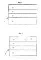
- FIG. 1represents a blank or undeveloped photomask of the prior art
- FIG. 2represents the photomask of FIG. 1 after it has been partially processed
- FIG. 3represents the photomask of FIGS. 1 and 2 after it has been fully processed
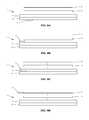
- FIG. 4is a flowchart showing the method of using a processed photomask to make or process a semiconductor wafer
- FIG. 5shows the process of making a semiconductor using a wafer stepper
- FIG. 6is a block diagram of a system for monitoring an integrated circuit manufacturing process according to an exemplary embodiment of the present invention.
- FIG. 7is a plan view of a photomask according to an exemplary embodiment of the present invention.
- FIGS. 8A-8Dare cross sectional views of a photomask according to an exemplary embodiment of the present invention.
- FIGS. 9A-9Bare cross-sectional view of a photomask according to an exemplary embodiment of the present invention.
- FIG. 10is a flowchart showing a method for monitoring a photomask according to an exemplary embodiment of the present invention.
- FIG. 11is a flowchart showing a method for monitoring a wafer manufacturing process using a feedback loop according to an exemplary embodiment of the present invention.
- FIG. 12is a flowchart showing a method for inspecting a photomask using a feedback loop according to an exemplary embodiment of the present invention.
- Various exemplary embodiments of the present inventionare directed to a photomask having electronics and detection capability integrated into the photomask substrate to enable wireless or other type of communication of information between the photomask and other elements of mask and wafer manufacturing processes including but not limited to mask making equipment, wafer exposure equipment, design automation tools, simulation tools, process control systems and mask tracking/logistical/shipping systems.
- the inventive photomaskpreferably has the ability to detect irradiation used to expose photomasks onto a wafer, such as, for example, 193 nm laser light in a wafer exposure scanner or other appropriate wavelength laser light. As explained in further detail below, such detected information may to be stored and analyzed for improving process capability.
- PhotomaskInformation relevant to the manufacturing of the photomask, such as pattern metrology data, defects, and registration information, as well as information capturing certain characteristics of the device layout written on the photomask, such as frequency composition of the layout, criticality of certain areas of the layout and tolerances required for creating a functioning device may also be stored using the components of the inventive photomask.
- the photomask according to various exemplary embodiments of the present inventionmay include computational logic needed to draw specific conclusions from stored data and to interact productively with complementary members of the manufacturing process.
- the inventive photomaskmay be used in a closed or open loop manufacturing process to accomplish tasks such as passing of layout specific data to a wafer exposure system in order to optimize the printing of the mask pattern on the wafer, passing of information from the mask to a simulation system to assess the manufacturing attributes of the mask, passing of the manufactured characteristics of the mask into a process control system, monitoring and characterization of the wafer exposure in terms of exposure level, vibration, position, mask illumination characteristics, scattered light etc., monitoring of the physical location of the mask for use in a logistical control system, measurement of the image characteristics in a reflected light mode, and passing of information to a centralized database to allow automated record keeping on mask characteristics, simulation results, exposure information and so on.
- taskssuch as passing of layout specific data to a wafer exposure system in order to optimize the printing of the mask pattern on the wafer, passing of information from the mask to a simulation system to assess the manufacturing attributes of the mask, passing of the manufactured characteristics of the mask into a process control system, monitoring and characterization of the wafer exposure in terms of exposure level, vibration
- the inventive photomaskmay be used to monitor an integrated circuit manufacturing environment, either prior to, during, or after the actual manufacturing process.
- the term “monitor”is intended to encompass any action that the inventive photomask may take relative to the manufacturing environment, such as, for example, measuring, diagnosing, characterizing, transmitting, receiving, testing, and optimizing.
- integrated circuitsas used herein is intended to cover any devices that include an electric circuit, having semiconductor components or otherwise, including but not limited to display devices, such as liquid crystal displays and plasma displays, microcontrollers, memory devices, processors, sensors, power management circuits and amplifiers.
- display devicessuch as liquid crystal displays and plasma displays, microcontrollers, memory devices, processors, sensors, power management circuits and amplifiers.
- FIG. 6shows a system, generally designated by reference number 1 , for monitoring an integrated circuit manufacturing process according to an exemplary embodiment of the present invention.
- the system 1includes a photomask 10 , a sensing station 20 , a computer workstation 30 , a photomask database 40 , an exposure tool, such as microlithographic tool 60 , as well as other wafer manufacturing components 50 .
- FIG. 7is a detailed plan view of the photomask 10 according to an exemplary embodiment of the present invention.
- the photomask 10includes a non-active patterned area 12 , an active patterned area 14 and a non-active non-patterned area 14 .
- a detection systemincluding various detection modules DM 1 , DM 2 , DM 3 and DM 4 , is integrated into the photomask 10 .
- the detection systemis capable of detecting at least one characteristic and preferably able to sense more than one characteristic of the photomask and/or manufacturing process parameters.
- the detection modules DM 1 -DM 4may be located at different regions within the photomask. For example, FIG.
- the detection module DM 2shows the detection module DM 1 located in non-active non-patterned region 14 , the detection module DM 2 located in non-active patterned area 12 , and the detection module DM 3 located in active patterned area 13 .
- the detection module DM 4may be located in the pellicle plane or at some other standoff distance from the primary mask pattern.
- the detection modules DM 1 -DM 4may include circuitry that is capable of detecting and/or monitoring any type of desired information, such as, for example, exposure level, vibration, position, illumination characteristics, scattered light, diffracted light, image characteristics in a reflected light mode, and the physical location of the photomask.
- the detection systemmay also include a photochemical recording medium, such as, for example, a photoresist, that is able to record a signal at the photomask 10 that may be analyzed later using standalone measurement equipment.
- a photochemical recording mediumsuch as, for example, a photoresist
- FIGS. 8A-Dshows a photoresist 98 included with the photomask 10 , where the photomask 10 includes a first substrate 91 , a second substrate 92 , one or more layers 94 and a pellicle layer 96 .
- the photoresist 98may be disposed at the bottom of the photomask 10 ( FIG. 8A ), at the top of the photomask 10 ( FIG. 8B ), between the two substrates 91 , 92 at the mask plane ( FIG. 8C ), at the pellicle plane ( FIG. 8D ) or at any other suitable location on or external to the photomask 10 .
- the photomask 10also includes a communication system 16 , which preferably includes a wireless transmitter, that sends information gathered by the detections modules DM 1 -DM 4 to the sensing station 20 .
- the sensing station 20may include a wireless receiver for retrieving the information transmitted by the communication system 16 .
- the photomask 10may include an interface for connection of hard wiring or a memory storage device such as a memory stick.
- the photomask 10further includes a memory system 18 that uses a storage medium, such as a flash memory.
- the memory system 18is preferably configured to store monitored process parameters and photomask manufacturing information.
- the memory system 18may store pattern metrology data, a defect profile, registration information, critical dimensions, layout characteristics, image fidelity and materials information.
- the memory system 18may also store, either separately or with other information, device layout information, such as, for example, frequency composition of the layout, information relating to criticality of selected areas of the layout, and required tolerances for creating a functioning device.
- the photomask 10may also include a logic processing unit 20 to manipulate data stored in the memory system 18 and/or data retrieved by the detection system to generate information to be transmitted to the sensing station 20 .
- software 22may be integrated into the photomask 10 that generates instructions to be run on the logic processing system 20 to carry out the analysis of data and/or manage the operation of electronics that connect the detection system, the memory system 18 and the logic processing unit 20 .
- the computer workstation 30may be accessed by a user to monitor the information retrieved by the sensing station 20 from the photomask 10 , and make adjustments to the manufacturing components 50 based on the information transmitted by the photomask 10 .
- the computer workstation 30may include software and or/hardware that automatically adjusts operation of the manufacturing components 50 based on the transmitted information, so that feedback loops may be generated between the photomask 10 and the manufacturing components 50 .
- the mask database 40may be used to store and maintain mask and process specific information. The mask database 40 may be maintained at the computer workstation 30 or at a remote location, and may be integrated into a network for access by other users.
- the photomask 10may also include a test structure 24 that diffracts, directs or otherwise conditions input radiation of a desired frequency or wavelength to render a more meaningful measurement on the electronic or photochemical detectors.
- the test structures 24may be placed on the top, bottom or pellicle areas of the photomask.
- the test structure 24includes a diffraction grating on the top of the mask that works in concert with the detection plane.
- Such test structuresmay contain moving parts as in an integrated microelectromechanical systems (MEMS) device or an oscillating device.
- MEMSmicroelectromechanical systems
- the photomask 10may also include a security system 26 for validating and securing the content of the photomask 10 .
- the security system 26may incorporate other components of the photomask 10 , such as the communication system 16 and the detection system.
- the communication system 16may be used to pass an encrypted signal or code to a manufacturing tool to validate the connection of the mask to the tool. Once the connection is validated, the communication system 16 may pass critical information to the tool which is necessary to initialize or continue the manufacturing process.
- the security system 26may also incorporate an optical detector from the detection system that can detect a scattered light thumbprint of the photomask 10 to ensure that the photomask 10 has not been manipulated or replaced in the chip fabrication process.
- the security system 26may also include a thin film or physical blocking aperture that is opened to allow exposure and interrogation of the pattern on the photomask 10 only when certain information is passed to the photomask system.
- the blocking apertureis physically embedded in the photomask itself so that the photomask is not inspectable or able to be exposed while the blocking aperture is enabled.
- the blocking aperturemay also be external to the photomask.
- a blocking aperture made of an electrochromic film 15may be placed under an absorbing layer 17 of the photomask 10 .
- electrochromic filmscan be made transparent through the introduction of an electric charge.
- Other blocking aperturesare possible based on mechanical and/or optical means. The blocking aperture may be disabled through a validation step with the wireless detector or with other methods consistent with secure applications.
- FIG. 10is a flowchart showing a method, generally designated by reference number 100 , for monitoring a photomask according to an exemplary embodiment of the present invention.
- a photomaskis manufactured based on customer requirements using processes well known in the art.
- critical informationis loaded into a mask database during the manufacturing process. Such critical information may include, for example, critical dimensions, layout characteristics, defect profile, registration, image fidelity, and materials information.
- step S 106the status of the photomask is updated and the status information is sent to the customer and production control.
- step S 108it is determined whether manufacture of the photomask is complete. If not, the process 100 returns to step S 102 , where manufacturing continues. Otherwise, the process 100 continues to step S 110 , where the mask database is loaded into the mask electronics module, which can be located either on the photomask or at a remote location.
- step S 112the photomask is shipped and may be electronically tracked using the communication system within the photomask.
- step S 114either prior to or upon arrival at the manufacturing site, the mask database is loaded into various components, such as a simulation system, an exposure system and a fab control system.
- step S 116the mask database is updated with wafer exposure characteristics.
- step S 118the information within the mask database, including the critical mask information and the wafer exposure characteristics, is used to adjust manufacturing parameters prior to and during manufacture of the wafer using the photomask.
- FIG. 11is a flowchart showing a method, generally designed by reference number 200 , for monitoring a wafer manufacturing process using a feedback loop according to an exemplary embodiment of the present invention.
- a photomask according to the present inventionis loaded into an exposure tool.
- information gathered by the detecting system on the photomask or stored in the memory on the photomaskis transmitted to a computer workstation. For example, information regarding diffracted light from the mask as detected by the detection system, or information regarding across field critical dimension variation or pattern layout stored within the memory of the photomask may be transmitted.
- the information transmitted by the photomaskis used to monitor and/or adjust manufacturing parameters, as appropriate.
- intensity detected in step S 204may be compared with a database image of an expected result to monitor the effectiveness of the mask.
- the operation of the exposure toolmay be adjusted to compensate for CD error by introducing a dose variation.
- the exposure tool sourcemay be optimized based on the layout data.
- FIG. 12is a flowchart showing a method, generally designated by reference number 300 , for inspecting a photomask using a feedback loop according to an exemplary embodiment of the present invention.
- the photomaskis loaded into an inspection tool.
- step S 304critical area information stored within the photomask memory is transmitted to the inspection tool.
- step S 306defect scoring is obtained using the critical area information transmitted by the photomask.
Landscapes
- Physics & Mathematics (AREA)
- General Physics & Mathematics (AREA)
- Exposure And Positioning Against Photoresist Photosensitive Materials (AREA)
Abstract
Description
- This application is a divisional application based on U.S. patent application Ser. No. 11/788,473, filed Apr. 20, 2007 and entitled PHOTOMASK WITH DETECTOR FOR OPTIMIZING AN INTEGRATED CIRCUIT PRODUCTION PROCESS AND METHOD OF MANUFACTURING AN INTEGRATED CIRCUIT USING THE SAME, the contents of which are incorporated herein by reference in their entirety.
- The present invention generally relates to photomasks and optical lithography for fabrication of integrated circuits. The present invention also generally relates to a method of manufacturing integrated circuits using photomasks.
- Photomasks are high precision plates containing microscopic images of electronic circuits. Photomasks are typically made from very flat pieces of quartz or glass with a layer of chrome on one side. Etched in the chrome is a portion of an electronic circuit design. This circuit design on the mask is also called “geometry.”
- A typical photomask used in the production of semiconductor devices is formed from a “blank” or “undeveloped” photomask. As shown in
FIG. 1 , a typicalblank photomask 5 is comprised of three or four layers. Thefirst layer 11 is a layer of quartz or other substantially transparent material, commonly referred to as the substrate. The next layer is typically a layer ofopaque material 12, such as Cr, which often includes a third layer ofantireflective material 13, such as CrO. The antireflective layer may or may not be included in any given photomask. The top layer is typically a layer ofphotosensitive resist material 14. Other types of photomasks are also known and used including, but not limited to, phase shift masks, embedded attenuated phase shift masks (“EAPSM”) and alternating aperture phase shift masks (“AAPSM”). These types of phase shift masks are characterized by design features including opaque regions and partially transparent regions through which the phase of light is shifted by, for example, approximately 180°. Examples of such photomasks are described in U.S. Pat. No. 6,682,861, U.S. Patent Publication No. 2004-0185348 A1, U.S. Patent Publication No. 2005-0026053 and U.S. Patent Publication No. 2005-0053847 to Photronics, Inc., the contents of which are incorporated by reference herein. - The process of manufacturing a photomask involves many steps and can be time consuming. In this regard, to manufacturer a photomask, the desired pattern of
opaque material 12 to be created on thephotomask 5 is typically defined by an electronic data file loaded into an exposure system which typically scans an electron beam (E-beam) or laser beam in a raster or vector fashion across the blank photomask. One such example of a raster scan exposure system is described in U.S. Pat. No. 3,900,737 to Collier. Each unique exposure system has its own software and format for processing data to instruct the equipment in exposing the blank photomask. As the E-beam or laser beam is scanned across theblank photomask 10, the exposure system directs the E-beam or laser beam at addressable locations on the photomask as defined by the electronic data file. The areas of the photosensitive resist material that are exposed to the E-beam or laser beam become soluble while the unexposed portions remain insoluble. - In order to determine where the e-beam or laser should expose the
photoresist 14 on theblank photomask 5, and where it should not, appropriate instructions to the processing equipment need to be provided, in the form of a jobdeck. In order to create the jobdeck the images of the desired pattern are broken up (or fractured) into smaller standardized shapes, e.g., rectangles and trapezoids. The fracturing process can be very time consuming. After being fractured, the image may need to be further modified by, for example, sizing the data if needed, rotating the data if needed, adding fiducial and internal reference marks, etc. Typically a dedicated computer system is used to perform the fracturing and/or create the jobdecks. The jobdeck data must then be transferred to the processing tools, to provide such tools with the necessary instructions to expose the photomask. - After the exposure system has scanned the desired image onto the
photosensitive resist material 14, as shown inFIG. 2 , the soluble photosensitive resist material is removed by means well known in the art, and the unexposed, insolublephotosensitive resist material 14′ remains adhered to theopaque material photomask 5 is formed by the remainingphotosensitive resist material 14′. - The pattern is then transferred from the remaining
photoresist material 14′ to thephotomask 5 via known etch processes to remove theantireflective material 13 andopaque materials 12 in regions which are not covered by theremaining photoresist 14′. There is a wide variety of etching processes known in the art, including dry etching as well as wet etching, and thus a wide variety of equipment is used to perform such etching. After etching is complete, the remainingphotoresist material 14′ is stripped or removed and the photomask is completed, as shown inFIG. 3 . In the completed photomask, the pattern as previously reflected by the remainingantireflective material 13′ andopaque materials 12′ are located in regions where theremaining photoresist 14′ remain after the soluble materials were removed in prior steps. - In order to determine if there are any unacceptable defects in a particular photomask, it is necessary to inspect the photomask. A defect is any flaw affecting the geometry. This includes undesirable chrome areas (chrome spots, chrome extensions, chrome bridging between geometry) or unwanted clear areas (pin holes, clear extensions, clear breaks). A defect can cause the circuit to be made from the photomask not to function. The entity ordering the photomask will indicate in its defect specification the size of defects that will affect its process. All defects of that size and larger must be repaired, or if they cannot be repaired, the mask must be rejected and rewritten.
- Typically, automated mask inspection systems, such as those manufactured by KLA-Tencor or Applied Materials, are used to detect defects. Such automated systems direct an illumination beam at the photomask and detect the intensity of the portion of the light beam transmitted through and reflected back from the photomask. The detected light intensity is then compared with expected light intensity, and any deviation is noted as a defect. The details of one system can be found in U.S. Pat. No. 5,563,702 assigned to KLA-Tencor.
- After passing inspection, a completed photomask is cleaned of contaminants. Next, a pellicle may be applied to the completed photomask to protect its critical pattern region from airborne contamination. Subsequent through pellicle defect inspection may be performed. In some instances, the photomask may be cut either before or after a pellicle is applied.
- Before performing each of the manufacturing steps described above, a semiconductor manufacturer (e.g., customer) must first provide a photomask manufacturer with different types of data relating to the photomask to be manufactured. In this regard, a customer typically provides a photomask order which includes various types of information and data which are needed to manufacture and process the photomask, including, for example, data relating to the design of the photomask, materials to be used, delivery dates, billing information and other information needed to process the order and manufacture the photomask.
- After the manufacturing steps described above are completed, the completed photomask is sent to a customer for use to manufacture semiconductor and other products. In particular, photomasks are commonly used in the semiconductor industry to transfer micro-scale images defining a semiconductor circuit onto a silicon or gallium arsenide substrate or wafer. The process for transferring an image from a photomask to a silicon substrate or wafer is commonly referred to as lithography or microlithography. Typically, as shown in
FIG. 4 , the semiconductor manufacturing process comprises the steps of deposition, photolithography, and etching. During deposition, a layer of either electrically insulating or electrically conductive material (like a metal, polysilicon or oxide) is deposited on the surface of a silicon wafer. This material is then coated with a photosensitive resist. The photomask is then used much the same way a photographic negative is used to make a photograph. Photolithography involves projecting the image on the photomask onto the wafer. If the image on the photomask is projected several times side by side onto the wafer, this is known as stepping and the photomask is called a reticle. - As shown in
FIG. 5 , to create an image21 on asemiconductor wafer 20, aphotomask 5 is interposed between thesemiconductor wafer 20, which includes a layer of photosensitive material, and anoptical system 22. Energy generated by an energy source23, commonly referred to as a Stepper, is inhibited from passing through the areas of thephotomask 5 where the opaque material is present. Energy from the Stepper23 passes through the transparent portions of thequartz substrate 11 not covered by theopaque material 12 and theantireflective material 13. Theoptical system 22 projects a scaledimage 24 of the pattern of theopaque material semiconductor wafer 20 and causes a reaction in the photosensitive material on the semiconductor wafer. The solubility of the photosensitive material is changed in areas exposed to the energy. In the case of a positive photolithographic process, the exposed photosensitive material becomes soluble and can be removed. In the case of a negative photolithographic process, the exposed photosensitive material becomes insoluble and unexposed soluble photosensitive material is removed. - After the soluble photosensitive material is removed, the image or pattern formed in the insoluble photosensitive material is transferred to the substrate by a process well known in the art which is commonly referred to as etching. Once the pattern is etched onto the substrate material, the remaining resist is removed resulting in a finished product. A new layer of material and resist is then deposited on the wafer and the image on the next photomask is projected onto it. Again the wafer is developed and etched. This process is repeated until the circuit is complete. Because, in a typical semiconductor device many layers may be deposited, many different photomasks may be necessary for the manufacture of even a single semiconductor device. Indeed, if more than one piece of equipment is used by a semiconductor manufacturer to manufacture a semiconductor device, it is possible more than one photomask may be needed, even for each layer. Furthermore, because different types of equipment may also be used to expose the photoresist in the different production lines, even the multiple identical photomask patterns may require additional variations in sizing, orientation, scaling and other attributes to account for differences in the semiconductor manufacturing equipment. Similar adjustments may also be necessary to account for differences in the photomask manufacturer's lithography equipment. These differences need to be accounted for in the photomask manufacturing process.
- Conventional integrated circuit manufacturing processes using photomasks require monitoring and adjustment on a frequent basis to optimize the quality of the final product and prevent errors from occurring. In this regard, information regarding, among other things, structural features of the photomask, the integrated circuit to be manufactured using the photomask, process parameters, and performance characteristics of the photomask, must be gathered, stored and regularly updated during the manufacturing process. This often requires numerous interruptions of the overall manufacturing process to conduct steps such as simulation of the photomask performance and sampling of the integrated circuit to determine whether adjustments to the process are required. For example, a sampling procedure may reveal that one or more manufacturing tools must be adjusted to compensate for errors or defects in the integrated circuit. The time required to sample the integrated circuit and perform other monitoring steps, analyze the results, and make the necessary adjustments to the manufacturing process may result in substantial delays, thereby generating a lower yield and a reduced overall profit margin for the integrated circuit manufacturer.
- Also, it is important to provide protections against unauthorized actions with a photomask, either prior to, during, or after a manufacturing process using the photomask. The photomask is generally considered to be an “unsafe” or “unsecure” medium for electronics design information. This is for three primary reasons: a) the photomask is the first physical and measurable record of the electronic design information; b) the electronics design information, once recorded on the mask, cannot be encrypted or scrambled (it is possible however to manipulate the mask content in selective ways with mask repair equipment); and c) once the photomask is recorded on a wafer through wafer exposure by an optical imaging system, the wafer pattern reveals additional measurable information about the device pattern. In the extreme case, the device can be fabricated in whole in or in part by an unauthorized source if the masks are in the parties' possession.
- As an example, photomasks used to fabricate military, government or personal information sensitive devices must be assured against manipulation or copy. Also, such protections is desirable for photomasks used to fabricate commercial devices in highly competitive applications, such as, for example, dynamic random access memories (DRAMs) and flash memories. An added concern in these applications is the relative simplicity of the patterns and the amount of competitive information that can be acquired through even visual inspection of the photomasks or patterned wafers.
- Protection may also be necessary for photomasks used to evaluate new equipment or test new modules of technology in a multi-company or multi-party environment. This is especially important given the pervasive use of multi-company consortia for early research and development. In particular, the initial evaluation of equipment for new process nodes requires the most advanced mask information in a nominally uncontrolled environment such as a fabrication facility for equipment owned by a third party.
- Providing protection for photomasks used to generally build devices in “wafer foundries” is also important. Securing and tracking intellectual property within the IC production process remains a key concern for end users.
- Actions of unauthorized users that mask owners and other interested parties may seek to prevent include exposure of the mask on a wafer by a wafer exposure system, reverse engineering of the mask content by scanning the features of the mask with an electronic imaging system such as a mask inspection system, and manipulation of the mask content for purposes of changing the electrical properties of devices being fabricated by the mask. In the case of unauthorized mask exposure, such exposure may be used to partially or completely fabricate the device intended to be manufactured using the mask, reverse engineer the device or otherwise discover the elements of the device.
- Photomasks are provided with some protection against unauthorized use using several conventional methods. For example, mask information may be scanned with a mask inspection or mask measuring system and compared to an electronic version of the design database. This can be used to test against mask manipulation when compared to a verified database. However, this protection method cannot prevent unauthorized exposure of the mask or physically secure the content on the mask. Alternatively, the layers of a full device can be separated to minimize the chance of reverse engineering the device content. In this case, half the device layers might be sent to foundry A while the other half might go to foundry B. Another protection method includes escorting the mask through the process by a designated security official. In general, there is no way at present to physically validate and secure the content of a mask at the point of use.
- Accordingly, there is a need for a photomask that allows for, among other things, monitoring, analyzing and storing of information regarding an integrated circuit manufacturing process that uses the photomask, without requiring interruption of the manufacturing process, while separately providing a secure environment for the use of the photomask.
- A photomask for integrated circuit production according to an exemplary embodiment of the present invention comprises a substrate, one or more layers, a detector for monitoring a process parameter of the integrated circuit production, and communication circuitry for communicating with external equipment for the integrated circuit production.
- In at least one embodiment, the detector comprises one or more sensors for detecting optical radiation.
- In at least one embodiment, the one or more sensors are designed to detect optical radiation from a wafer exposure scanner.
- In at least one embodiment, the process parameter comprises a parameter of a stepper for the integrated circuit production.
- In at least one embodiment, the one or more layers comprise an active portion and a non-active portion.
- In at least one embodiment, the detector is positioned at the active portion.
- In at least one embodiment, the detector is positioned at the non-active portion.
- In at least one embodiment, the one or more layers comprise a patterned portion and a non-patterned portion.
- In at least one embodiment, the detector is positioned at the patterned portion.
- In at least one embodiment, the detector is positioned at the non-patterned portion.
- In at least one embodiment, the detector is positioned at a predetermined distance from the patterned portion.
- In at least one embodiment, the detector is positioned at the substrate.
- In at least one embodiment, further comprising a pellicle.
- In at least one embodiment, the detector is positioned at least partially at the pellicle plane.
- In at least one embodiment, the detector comprises at least one type of circuitry selected from the group consisting of: circuitry for monitoring an exposure level, circuitry for monitoring a vibration, circuitry for monitoring a position, circuitry for monitoring illumination characteristics, circuitry for monitoring scattered light, circuitry for monitoring diffracted light, circuitry for measuring image characteristics in a reflected light mode, and circuitry for monitoring the physical location of the photomask.
- In at least one embodiment, the communication circuitry comprises wireless communication circuitry.
- In at least one embodiment, the communication circuitry comprises wired communication circuitry.
- In at least one embodiment, the external equipment comprises at least one type of external equipment selected from the group consisting of: photomask manufacturing equipment, wafer exposure equipment, a design automation tool, a simulation tool, a process control system, a logistical control system, a mask tracking system, a shipping system, a central database, a computer workstation, and a sensing station.
- In at least one embodiment, the photomask further comprises a computational processor for analyzing the monitored process parameter.
- In at least one embodiment, the photomask further comprises a data storage component.
- In at least one embodiment, the data storage component comprises a flash memory.
- In at least one embodiment, the data storage component comprises a memory for storing the monitored process parameter.
- In at least one embodiment, the data storage component comprises a memory for storing photomask manufacturing information.
- In at least one embodiment, the photomask manufacturing information comprises at least one type of information selected from the group consisting of: pattern metrology data, a defect profile, registration information, critical dimensions, layout characteristics, image fidelity, and materials information.
- In at least one embodiment, the data storage component comprises a memory for storing device layout information.
- In at least one embodiment, the device layout information comprises at least one type of information selected from the group consisting of: frequency composition of the layout, information relating to criticality of selected areas of the layout, and required tolerances for creating a functioning device.
- In at least one embodiment, the detector comprises a photochemical detector.
- In at least one embodiment, the photochemical detector comprises a photoresist.
- In at least one embodiment, the communication circuitry comprises circuitry for communication signals recorded in the photochemical detector to stand-alone measurement equipment.
- In at least one embodiment, the photochemical detector is positioned at a top surface of the photomask.
- In at least one embodiment, the photochemical detector is positioned at a bottom surface of the photomask.
- In at least one embodiment, the photochemical detector is positioned on a mask plane between the substrate and the one or more layers.
- In at least one embodiment, the photochemical detector is positioned within the one or more layers.
- In at least one embodiment, the photomask further comprises a pellicle, and the photochemical recording medium is positioned in a pellicle plane.
- In at least one embodiment, the photomask further comprises a test structure for conditioning the process parameter to be monitored by the detector.
- In at least one embodiment, the test structure is designed to diffract optical radiation.
- In at least one embodiment, the test structure comprises a diffraction grating.
- In at least one embodiment, the test structure is designed to reflect optical radiations.
- In at least one embodiment, the test structure is designed to scatter optical radiation.
- In at least one embodiment, the test structure is designed to direct optical radiation to the detector.
- In at least one embodiment, the test structure is positioned at a top surface of the photomask.
- In at least one embodiment, the test structure is positioned at a bottom surface of the photomask.
- In at least one embodiment, the photomask further comprises a pellicle, and the test structure is positioned at the pellicle plane.
- In at least one embodiment, the test structure comprises moving parts.
- In at least one embodiment, the test structure comprises an oscillating device.
- In at least one embodiment, the test structure comprises an integrated microelectromechanical systems (MEMS) device.
- In at least one embodiment, the photomask further comprises a security system that prevents at least one of unauthorized use and copying of the photomask.
- In at least one embodiment, wherein the security system comprises at least a portion of the communication circuitry and transmits signals to one or more of the external equipment to validate connection of the photomask with the one or more external equipment.
- In at least one embodiment, the transmitted signals are encrypted.
- In at least one embodiment, the detector comprises one or more sensors, and the security system comprises at least one of the one or more sensors to detect characteristics of the photomask to ensure that the photomask was not subjected to at least one of manipulation and replacement.
- In at least one embodiment, the at least one sensor is an optical sensor.
- In at least one embodiment, the at least one sensor detects a scattered light thumbprint of the photomask.
- In at least one embodiment, the security system comprises a blocking aperture.
- In at least one embodiment, the blocking aperture is disposed on the photomask.
- In at least one embodiment, the blocking aperture is disposed within the photomask.
- In at least one embodiment, the blocking aperture is external to the photomask.
- In at least one embodiment, the blocking aperture comprises a thin film.
- In at least one embodiment, the thin film is an electrochromic film.
- In at least one embodiment, the photomask is a binary photomask.
- In at least one embodiment, the photomask is an embedded attenuated phase shift mask.
- In at least one embodiment, the photomask is an alternating aperture phase shift mask.
- A method of integrated circuit production according to an exemplary embodiment of the present invention comprises the steps of: providing a photomask with circuitry in the integrated circuit production process; monitoring a process parameter of the integrated circuit production using the photomask; and analyzing the monitored process parameter using the photomask.
- In at least one embodiment, the process parameter comprises at least one process parameter selected from the group consisting of: optical radiation, exposure level, vibration, position, illumination characteristics, scattered light, diffracted light, image characteristics in a reflected light mode, and physical location of the photomask.
- In at least one embodiment, the method further comprises the step of adjusting the integrated circuit production process based on the result of the analyzing step.
- In at least one embodiment, the analyzing step comprises the step of comparing the results of the monitoring step with expected results stored in a memory device associated with the photomask.
- In at least one embodiment, the photomask comprises the memory device.
- In at least one embodiment, the analyzing step comprises the step of processing the monitored process parameter using computational logic.
- In at least one embodiment, the method further comprises the step of communicating the result of the analyzing step from the photomask to external equipment involved in the integrated circuit production.
- In at least one embodiment, the external equipment comprises at least one type of equipment selected from the group consisting of: photomask manufacturing equipment, wafer exposure equipment, a design automation tool, a simulation tool, a process control system, a central database, a computer workstation, and a sensing station.
- In at least one embodiment, the method further comprises the step of storing the monitored process parameter in the photomask.
- In at least one embodiment, the method further comprises the step of storing the result of the analyzing step in the photomask.
- In at least one embodiment, the method further comprises, prior to the monitoring step, the step of conditioning the process monitor to be monitored using the photomask.
- In at least one embodiment, the conditioning step comprises the step of diffracting optical radiation using the photomask.
- In at least one embodiment, the conditioning step comprises the step of reflecting optical radiation using the photomask.
- In at least one embodiment, the conditioning step comprises the step of scattering optical radiation using the photomask.
- In at least one embodiment, the conditioning step comprises the step of directing optical radiation toward a detection plane using the photomask.
- In at least one embodiment, the step of monitoring comprises detecting the process parameter using electronic detection circuitry.
- In at least one embodiment, the step of monitoring comprises detecting the process parameter using a photochemical detector.
- In at least one embodiment, the photochemical detector comprises a photoresist.
- In at least one embodiment, the method further comprises a step of securing the photomask against at least one of unauthorized use and copying.
- In at least one embodiment, the step of securing comprises transmitting signals to one or more of the external equipment to validate connection of the photomask with the one or more external equipment.
- In at least one embodiment, the method further comprises a step of encrypting the signals.
- In at least one embodiment, the step of securing comprises detecting one or more characteristics of the photomask to ensure that the photomask was not subjected to at least one of manipulation and replacement.
- In at least one embodiment, the one or more characteristics comprises a scattered light thumbprint of the photomask.
- In at least one embodiment, the step of securing comprises selectively blocking the photomask with a blocking aperture.
- The above and related objects, features and advantages of the present invention will be more fully understood by reference to the following, detailed description of the preferred, albeit illustrative, embodiment of the present invention when taken in conjunction with the accompanying figures, wherein:
FIG. 1 represents a blank or undeveloped photomask of the prior art;FIG. 2 represents the photomask ofFIG. 1 after it has been partially processed;FIG. 3 represents the photomask ofFIGS. 1 and 2 after it has been fully processed;FIG. 4 is a flowchart showing the method of using a processed photomask to make or process a semiconductor wafer;FIG. 5 shows the process of making a semiconductor using a wafer stepper;FIG. 6 is a block diagram of a system for monitoring an integrated circuit manufacturing process according to an exemplary embodiment of the present invention;FIG. 7 is a plan view of a photomask according to an exemplary embodiment of the present invention;FIGS. 8A-8D are cross sectional views of a photomask according to an exemplary embodiment of the present invention;FIGS. 9A-9B are cross-sectional view of a photomask according to an exemplary embodiment of the present invention;FIG. 10 is a flowchart showing a method for monitoring a photomask according to an exemplary embodiment of the present invention;FIG. 11 is a flowchart showing a method for monitoring a wafer manufacturing process using a feedback loop according to an exemplary embodiment of the present invention; andFIG. 12 is a flowchart showing a method for inspecting a photomask using a feedback loop according to an exemplary embodiment of the present invention.- Various exemplary embodiments of the present invention are directed to a photomask having electronics and detection capability integrated into the photomask substrate to enable wireless or other type of communication of information between the photomask and other elements of mask and wafer manufacturing processes including but not limited to mask making equipment, wafer exposure equipment, design automation tools, simulation tools, process control systems and mask tracking/logistical/shipping systems. The inventive photomask preferably has the ability to detect irradiation used to expose photomasks onto a wafer, such as, for example, 193 nm laser light in a wafer exposure scanner or other appropriate wavelength laser light. As explained in further detail below, such detected information may to be stored and analyzed for improving process capability. Information relevant to the manufacturing of the photomask, such as pattern metrology data, defects, and registration information, as well as information capturing certain characteristics of the device layout written on the photomask, such as frequency composition of the layout, criticality of certain areas of the layout and tolerances required for creating a functioning device may also be stored using the components of the inventive photomask. In addition to storage capabilities, the photomask according to various exemplary embodiments of the present invention may include computational logic needed to draw specific conclusions from stored data and to interact productively with complementary members of the manufacturing process.
- The inventive photomask may be used in a closed or open loop manufacturing process to accomplish tasks such as passing of layout specific data to a wafer exposure system in order to optimize the printing of the mask pattern on the wafer, passing of information from the mask to a simulation system to assess the manufacturing attributes of the mask, passing of the manufactured characteristics of the mask into a process control system, monitoring and characterization of the wafer exposure in terms of exposure level, vibration, position, mask illumination characteristics, scattered light etc., monitoring of the physical location of the mask for use in a logistical control system, measurement of the image characteristics in a reflected light mode, and passing of information to a centralized database to allow automated record keeping on mask characteristics, simulation results, exposure information and so on. In general, the inventive photomask may be used to monitor an integrated circuit manufacturing environment, either prior to, during, or after the actual manufacturing process. For the purposes of this disclosure, the term “monitor” is intended to encompass any action that the inventive photomask may take relative to the manufacturing environment, such as, for example, measuring, diagnosing, characterizing, transmitting, receiving, testing, and optimizing.
- It should be appreciated that the present invention is applicable to the manufacture of integrated circuits, and the term “integrated circuits” as used herein is intended to cover any devices that include an electric circuit, having semiconductor components or otherwise, including but not limited to display devices, such as liquid crystal displays and plasma displays, microcontrollers, memory devices, processors, sensors, power management circuits and amplifiers.
FIG. 6 shows a system, generally designated by reference number1, for monitoring an integrated circuit manufacturing process according to an exemplary embodiment of the present invention. The system1 includes aphotomask 10, asensing station 20, acomputer workstation 30, aphotomask database 40, an exposure tool, such asmicrolithographic tool 60, as well as otherwafer manufacturing components 50.FIG. 7 is a detailed plan view of thephotomask 10 according to an exemplary embodiment of the present invention. Thephotomask 10 includes a non-active patternedarea 12, an active patternedarea 14 and a non-activenon-patterned area 14. A detection system, including various detection modules DM1, DM2, DM3 and DM4, is integrated into thephotomask 10. The detection system is capable of detecting at least one characteristic and preferably able to sense more than one characteristic of the photomask and/or manufacturing process parameters. In this regard, in order to fully detect and retrieve data from various locations on the photomask, the detection modules DM1-DM4 may be located at different regions within the photomask. For example,FIG. 2 shows the detection module DM1 located in non-activenon-patterned region 14, the detection module DM2 located in non-active patternedarea 12, and the detection module DM3 located in active patternedarea 13. The detection module DM4 may be located in the pellicle plane or at some other standoff distance from the primary mask pattern. The detection modules DM1-DM4 may include circuitry that is capable of detecting and/or monitoring any type of desired information, such as, for example, exposure level, vibration, position, illumination characteristics, scattered light, diffracted light, image characteristics in a reflected light mode, and the physical location of the photomask.- The detection system may also include a photochemical recording medium, such as, for example, a photoresist, that is able to record a signal at the
photomask 10 that may be analyzed later using standalone measurement equipment. For example,FIGS. 8A-D shows aphotoresist 98 included with thephotomask 10, where thephotomask 10 includes afirst substrate 91, asecond substrate 92, one ormore layers 94 and apellicle layer 96. Thephotoresist 98 may be disposed at the bottom of the photomask10 (FIG. 8A ), at the top of the photomask10 (FIG. 8B ), between the twosubstrates FIG. 8C ), at the pellicle plane (FIG. 8D ) or at any other suitable location on or external to thephotomask 10. - The
photomask 10 also includes acommunication system 16, which preferably includes a wireless transmitter, that sends information gathered by the detections modules DM1-DM4 to thesensing station 20. In this regard, thesensing station 20 may include a wireless receiver for retrieving the information transmitted by thecommunication system 16. In embodiments of the invention, thephotomask 10 may include an interface for connection of hard wiring or a memory storage device such as a memory stick. - The
photomask 10 further includes amemory system 18 that uses a storage medium, such as a flash memory. Thememory system 18 is preferably configured to store monitored process parameters and photomask manufacturing information. For example, thememory system 18 may store pattern metrology data, a defect profile, registration information, critical dimensions, layout characteristics, image fidelity and materials information. Thememory system 18 may also store, either separately or with other information, device layout information, such as, for example, frequency composition of the layout, information relating to criticality of selected areas of the layout, and required tolerances for creating a functioning device. - The
photomask 10 may also include alogic processing unit 20 to manipulate data stored in thememory system 18 and/or data retrieved by the detection system to generate information to be transmitted to thesensing station 20. In this regard,software 22 may be integrated into thephotomask 10 that generates instructions to be run on thelogic processing system 20 to carry out the analysis of data and/or manage the operation of electronics that connect the detection system, thememory system 18 and thelogic processing unit 20. - The
computer workstation 30 may be accessed by a user to monitor the information retrieved by thesensing station 20 from thephotomask 10, and make adjustments to themanufacturing components 50 based on the information transmitted by thephotomask 10. Alternatively, or in addition, thecomputer workstation 30 may include software and or/hardware that automatically adjusts operation of themanufacturing components 50 based on the transmitted information, so that feedback loops may be generated between thephotomask 10 and themanufacturing components 50. In this regard, themask database 40 may be used to store and maintain mask and process specific information. Themask database 40 may be maintained at thecomputer workstation 30 or at a remote location, and may be integrated into a network for access by other users. - The
photomask 10 may also include atest structure 24 that diffracts, directs or otherwise conditions input radiation of a desired frequency or wavelength to render a more meaningful measurement on the electronic or photochemical detectors. Thetest structures 24 may be placed on the top, bottom or pellicle areas of the photomask. In an exemplary embodiment, thetest structure 24 includes a diffraction grating on the top of the mask that works in concert with the detection plane. Such test structures may contain moving parts as in an integrated microelectromechanical systems (MEMS) device or an oscillating device. - The
photomask 10 may also include asecurity system 26 for validating and securing the content of thephotomask 10. Thesecurity system 26 may incorporate other components of thephotomask 10, such as thecommunication system 16 and the detection system. For example, thecommunication system 16 may be used to pass an encrypted signal or code to a manufacturing tool to validate the connection of the mask to the tool. Once the connection is validated, thecommunication system 16 may pass critical information to the tool which is necessary to initialize or continue the manufacturing process. Thesecurity system 26 may also incorporate an optical detector from the detection system that can detect a scattered light thumbprint of thephotomask 10 to ensure that thephotomask 10 has not been manipulated or replaced in the chip fabrication process. - The
security system 26 may also include a thin film or physical blocking aperture that is opened to allow exposure and interrogation of the pattern on thephotomask 10 only when certain information is passed to the photomask system. Preferably, the blocking aperture is physically embedded in the photomask itself so that the photomask is not inspectable or able to be exposed while the blocking aperture is enabled. However, the blocking aperture may also be external to the photomask. As an example, as shown inFIGS. 9A and 9B , a blocking aperture made of anelectrochromic film 15 may be placed under an absorbinglayer 17 of thephotomask 10. As known in the art, electrochromic films can be made transparent through the introduction of an electric charge. Other blocking apertures are possible based on mechanical and/or optical means. The blocking aperture may be disabled through a validation step with the wireless detector or with other methods consistent with secure applications. FIG. 10 is a flowchart showing a method, generally designated byreference number 100, for monitoring a photomask according to an exemplary embodiment of the present invention. In step S102, a photomask is manufactured based on customer requirements using processes well known in the art. In step S104, critical information is loaded into a mask database during the manufacturing process. Such critical information may include, for example, critical dimensions, layout characteristics, defect profile, registration, image fidelity, and materials information. In step S106, the status of the photomask is updated and the status information is sent to the customer and production control. In step S108, it is determined whether manufacture of the photomask is complete. If not, theprocess 100 returns to step S102, where manufacturing continues. Otherwise, theprocess 100 continues to step S110, where the mask database is loaded into the mask electronics module, which can be located either on the photomask or at a remote location.- In step S112, the photomask is shipped and may be electronically tracked using the communication system within the photomask. In step S114, either prior to or upon arrival at the manufacturing site, the mask database is loaded into various components, such as a simulation system, an exposure system and a fab control system. In step S116, the mask database is updated with wafer exposure characteristics. In step S118, the information within the mask database, including the critical mask information and the wafer exposure characteristics, is used to adjust manufacturing parameters prior to and during manufacture of the wafer using the photomask.
FIG. 11 is a flowchart showing a method, generally designed byreference number 200, for monitoring a wafer manufacturing process using a feedback loop according to an exemplary embodiment of the present invention. In step S202 of theprocess 200, a photomask according to the present invention is loaded into an exposure tool. In step S204, information gathered by the detecting system on the photomask or stored in the memory on the photomask is transmitted to a computer workstation. For example, information regarding diffracted light from the mask as detected by the detection system, or information regarding across field critical dimension variation or pattern layout stored within the memory of the photomask may be transmitted. In step S206, the information transmitted by the photomask is used to monitor and/or adjust manufacturing parameters, as appropriate. For example, intensity detected in step S204 may be compared with a database image of an expected result to monitor the effectiveness of the mask. In the case of the CD variation being transmitted by the photomask, the operation of the exposure tool may be adjusted to compensate for CD error by introducing a dose variation. In the case of the pattern layout being transmitted by the photomask, the exposure tool source may be optimized based on the layout data.FIG. 12 is a flowchart showing a method, generally designated byreference number 300, for inspecting a photomask using a feedback loop according to an exemplary embodiment of the present invention. In step S302 of theprocess 300, the photomask is loaded into an inspection tool. In step S304, critical area information stored within the photomask memory is transmitted to the inspection tool. In step S306, defect scoring is obtained using the critical area information transmitted by the photomask.- Now that the preferred embodiments of the present invention have been shown and described in detail, various modifications and improvements thereon will become readily apparent to those skilled in the art. The present embodiments are therefore to be considered in all respects as illustrative and not restrictive, the scope of the invention being indicated by the appended claims, and all changes that come within the meaning and range of equivalency of the claims are therefore intended to be embraced therein.
Claims (24)
Priority Applications (1)
| Application Number | Priority Date | Filing Date | Title |
|---|---|---|---|
| US12/727,342US7910269B2 (en) | 2007-04-20 | 2010-03-19 | Photomask with detector for optimizing an integrated circuit production process and method of manufacturing an integrated circuit using the same |
Applications Claiming Priority (2)
| Application Number | Priority Date | Filing Date | Title |
|---|---|---|---|
| US11/788,473US7790340B2 (en) | 2007-04-20 | 2007-04-20 | Photomask with detector for optimizing an integrated circuit production process and method of manufacturing an integrated circuit using the same |
| US12/727,342US7910269B2 (en) | 2007-04-20 | 2010-03-19 | Photomask with detector for optimizing an integrated circuit production process and method of manufacturing an integrated circuit using the same |
Related Parent Applications (1)
| Application Number | Title | Priority Date | Filing Date |
|---|---|---|---|
| US11/788,473DivisionUS7790340B2 (en) | 2007-04-20 | 2007-04-20 | Photomask with detector for optimizing an integrated circuit production process and method of manufacturing an integrated circuit using the same |
Publications (2)
| Publication Number | Publication Date |
|---|---|
| US20100174393A1true US20100174393A1 (en) | 2010-07-08 |
| US7910269B2 US7910269B2 (en) | 2011-03-22 |
Family
ID=39872543
Family Applications (2)
| Application Number | Title | Priority Date | Filing Date |
|---|---|---|---|
| US11/788,473Active2028-10-13US7790340B2 (en) | 2007-04-20 | 2007-04-20 | Photomask with detector for optimizing an integrated circuit production process and method of manufacturing an integrated circuit using the same |
| US12/727,342ActiveUS7910269B2 (en) | 2007-04-20 | 2010-03-19 | Photomask with detector for optimizing an integrated circuit production process and method of manufacturing an integrated circuit using the same |
Family Applications Before (1)
| Application Number | Title | Priority Date | Filing Date |
|---|---|---|---|
| US11/788,473Active2028-10-13US7790340B2 (en) | 2007-04-20 | 2007-04-20 | Photomask with detector for optimizing an integrated circuit production process and method of manufacturing an integrated circuit using the same |
Country Status (1)
| Country | Link |
|---|---|
| US (2) | US7790340B2 (en) |
Families Citing this family (8)
| Publication number | Priority date | Publication date | Assignee | Title |
|---|---|---|---|---|
| US7851110B2 (en)* | 2007-04-20 | 2010-12-14 | Photronics, Inc. | Secure photomask with blocking aperture |
| US7790340B2 (en)* | 2007-04-20 | 2010-09-07 | Photronics, Inc. | Photomask with detector for optimizing an integrated circuit production process and method of manufacturing an integrated circuit using the same |
| US8001492B2 (en)* | 2007-06-28 | 2011-08-16 | Linden Design Technologies, Inc. | Evaluation method for interconnects interacted with integrated-circuit manufacture |
| DE102008042463B3 (en)* | 2008-09-30 | 2010-04-22 | Carl Zeiss Smt Ag | Optical measuring device for a projection exposure apparatus |
| KR20130035144A (en)* | 2011-09-29 | 2013-04-08 | 삼성전자주식회사 | Display apparatus including a pattern and method for forming a pattern in the display apparatus |
| US10394116B2 (en) | 2017-09-06 | 2019-08-27 | International Business Machines Corporation | Semiconductor fabrication design rule loophole checking for design for manufacturability optimization |
| KR102722920B1 (en) | 2019-04-18 | 2024-10-28 | 삼성전자주식회사 | Measuring apparatus for vacuum chamber, and measuring system comprising the same |
| CN116341886B (en)* | 2023-05-31 | 2023-11-14 | 长鑫存储技术有限公司 | Method, system, device, equipment and medium for processing photomask resources |
Citations (63)
| Publication number | Priority date | Publication date | Assignee | Title |
|---|---|---|---|---|
| US4014602A (en)* | 1975-01-16 | 1977-03-29 | Siemens Aktiengesellschaft | Identification card having a hologram superimposed on printed data |
| US4477182A (en)* | 1981-07-10 | 1984-10-16 | Hitachi, Ltd. | Pattern exposing apparatus |
| US4576439A (en)* | 1982-09-15 | 1986-03-18 | Rca Corporation | Reflective diffractive authenticating device |
| US4662653A (en)* | 1984-01-03 | 1987-05-05 | Lgz Landis & Gyr Zug Ag | Optically diffracting security element |
| US4663625A (en)* | 1983-11-30 | 1987-05-05 | Motion Magnetics Inc. | Passive tag identification system and method |
| US5361307A (en)* | 1993-03-25 | 1994-11-01 | General Electric Company | Correlation methods of identifying defects in imaging devices |
| US5379131A (en)* | 1991-12-11 | 1995-01-03 | Dai Nippon Printing Co., Ltd. | Method of preventing forgery of diffraction grating pattern and forgery-proof diffraction grating pattern recording structure |
| US5528402A (en)* | 1994-02-07 | 1996-06-18 | Parker; William P. | Addressable electrohologram employing electro-optic layer and patterned conductor between two electrodes |
| US5734752A (en)* | 1996-09-24 | 1998-03-31 | Xerox Corporation | Digital watermarking using stochastic screen patterns |
| US5790703A (en)* | 1997-01-21 | 1998-08-04 | Xerox Corporation | Digital watermarking using conjugate halftone screens |
| US5909313A (en)* | 1993-05-25 | 1999-06-01 | Commonwealth Scientific And Industrial Research Organisation | Multiple image diffractive device |
| US5949055A (en)* | 1997-10-23 | 1999-09-07 | Xerox Corporation | Automatic geometric image transformations using embedded signals |
| US6001510A (en)* | 1994-08-15 | 1999-12-14 | Meng; Wu | Method for producing laser hologram anti-counterfeit mark with identifying card and inspecting card and inspecting apparatus for the mark |
| US6057082A (en)* | 1994-09-11 | 2000-05-02 | International Business Machines Corporation | Method of fabricating authentication labels and authenticating patterns incorporating diffraction structures |
| US6127069A (en)* | 1995-06-06 | 2000-10-03 | International Business Machines Corporation | Method of visually inspecting positioning of a pattern on a substrate |
| US6160782A (en)* | 1997-12-26 | 2000-12-12 | Victor Company Of Japan, Ltd. | Holographic storage medium and reproduction of data therefrom |
| US6207330B1 (en)* | 1997-07-14 | 2001-03-27 | International Business Machines Corporation | Formation of punch inspection masks and other devices using a laser |
| US6337752B1 (en)* | 1989-09-28 | 2002-01-08 | GAO Gesellschaft für Automation und Organisation mbH | Data carrier having an optically variable element and methods for producing it |
| US6359734B1 (en)* | 1997-06-06 | 2002-03-19 | Ovd Kinegram Ag | Surface pattern |
| US20020037461A1 (en)* | 2000-08-25 | 2002-03-28 | Van Der Werf Jan E. | Lithographic apparatus, device manufacturing method, and device manufactured thereby |
| US6421013B1 (en)* | 1999-10-04 | 2002-07-16 | Amerasia International Technology, Inc. | Tamper-resistant wireless article including an antenna |
| US6449377B1 (en)* | 1995-05-08 | 2002-09-10 | Digimarc Corporation | Methods and systems for watermark processing of line art images |
| US20020167653A1 (en)* | 1998-04-08 | 2002-11-14 | Asml Netherlands B.V. | Lithography apparatus |
| US20030052691A1 (en)* | 2001-06-06 | 2003-03-20 | Credence Technologies, Inc. | Apparatus and method for detection and measurement of environmental parameters |
| US6597427B1 (en)* | 1999-07-06 | 2003-07-22 | International Business Machines Corporation | Liquid crystal panel, display device, identification mark detection device, detection display system, TFT array repair device and identification mark detection method |
| US20030143472A1 (en)* | 2002-01-24 | 2003-07-31 | Yasuhiro Koizumi | Manufacturing method of photomask |
| US6610351B2 (en)* | 2000-04-12 | 2003-08-26 | Quantag Systems, Inc. | Raman-active taggants and their recognition |
| US6610446B2 (en)* | 2001-01-26 | 2003-08-26 | International Business Machines Corporation | Information storage on masks for microlithographic tools |
| US20030179277A1 (en)* | 2000-08-11 | 2003-09-25 | Stefan Stadler | Use of a data carrier for storing micro-images |
| US20040043308A1 (en)* | 2000-11-04 | 2004-03-04 | Norbert Lutz | Plastic body, which is provided in the form of a film, for example, a transfer film or laminate film or which is provided with a film of this type, and method for producing color image on or in a plastic body of this type |
| US6706314B2 (en)* | 2001-03-15 | 2004-03-16 | Amesbury Trust | Method of labelling an object |
| US6734931B2 (en)* | 2000-02-18 | 2004-05-11 | Lg.Philips Lcd Co., Ltd. | Color filter substrate having identification mark formed in the black matrix |
| US6740472B2 (en)* | 2002-06-03 | 2004-05-25 | Latent Image Technologies Ltd. | Polymer materials with independent latent images visible in polarized light and methods for their production |
| US20040121268A1 (en)* | 2001-06-06 | 2004-06-24 | Spectra Systems Corporation | Incorporation of markings in optical media |
| US6780564B2 (en)* | 1998-06-25 | 2004-08-24 | Flexplay Technologies, Inc. | Methods and apparatus for rendering an optically encoded medium unreadable and tamper-resistant |
| US6822769B1 (en)* | 1999-06-01 | 2004-11-23 | De La Rue International Limited | Security device |
| US20050008944A1 (en)* | 2003-07-10 | 2005-01-13 | Francesco Cerrina | Defect inspection of extreme ultraviolet lithography masks and the like |
| US20050019680A1 (en)* | 2001-10-09 | 2005-01-27 | Stephen Pinchen | Anti-counterfeit measures |
| US6855463B2 (en)* | 2002-08-27 | 2005-02-15 | Photronics, Inc. | Photomask having an intermediate inspection film layer |
| US6860927B2 (en)* | 2000-09-19 | 2005-03-01 | Merck Patent Gmbh | Polymer beads |
| US20050056441A1 (en)* | 2002-10-01 | 2005-03-17 | Rider Gavin Charles | Reduction of electric-field-induced damage in field-sensitive articles |
| US6882737B2 (en)* | 2000-12-21 | 2005-04-19 | Digimarc Corporation | Digitally watermarking holograms for identity documents |
| US6887650B2 (en)* | 2001-07-24 | 2005-05-03 | Seiko Epson Corporation | Transfer method, method of manufacturing thin film devices, method of manufacturing integrated circuits, circuit board and manufacturing method thereof, electro-optical apparatus and manufacturing method thereof, ic card, and electronic appliance |
| US6894766B1 (en)* | 2001-03-27 | 2005-05-17 | Dupont Photomasks, Inc. | Method for constructing a photomask assembly using an encoded mark |
| US6903850B2 (en)* | 2000-06-28 | 2005-06-07 | De La Rue International Limited | Security device |
| US20050134463A1 (en)* | 2003-12-19 | 2005-06-23 | Semiconductor Energy Laboratory Co., Ltd. | Semiconductor device, RFID tag and label-like object |
| US6924088B2 (en)* | 2002-06-20 | 2005-08-02 | Applied Materials, Inc. | Method and system for realtime CD microloading control |
| US6964837B2 (en)* | 2000-05-04 | 2005-11-15 | Basf Aktiengesellschaft | Utilization of beam crosslinkable polymer compositions as data recording medium |
| US20060043197A1 (en)* | 2004-08-31 | 2006-03-02 | Chang Yung C | Carrier facilitating radio-frequency identification (RFID) operation in a semiconductor fabrication system |
| US7057259B2 (en)* | 2001-03-21 | 2006-06-06 | Kabushiki Kaisha Toshiba | Semiconductor wafer with ID mark, equipment for and method of manufacturing semiconductor device from them |
| US7063924B2 (en)* | 2002-12-20 | 2006-06-20 | Eastman Kodak Company | Security device with patterned metallic reflection |
| US20060154180A1 (en)* | 2005-01-07 | 2006-07-13 | Kannurpatti Anandkumar R | Imaging element for use as a recording element and process of using the imaging element |
| US7108945B2 (en)* | 2002-03-27 | 2006-09-19 | Kabushiki Kaisha Toshiba | Photomask having a focus monitor pattern |
| US7108171B1 (en)* | 2002-07-02 | 2006-09-19 | Michael Jared Ergo | Methods of temporarily providing digital content to a customer |
| US20070037070A1 (en)* | 2005-08-12 | 2007-02-15 | Semiconductor Energy Laboratory Co., Ltd. | Light exposure mask and method for manufacturing semiconductor device using the same |
| US7204419B2 (en)* | 2003-05-01 | 2007-04-17 | Identifcation Dynamics, Llc | Method and apparatus for reading firearm microstamping |
| US7220535B2 (en)* | 2001-06-06 | 2007-05-22 | Spectra Systems Corporation | Marking and authenticating articles |
| US7234645B2 (en)* | 1997-03-16 | 2007-06-26 | Silverbrook Research Pty Ltd | Document having an encoded data structure |
| US20070148599A1 (en)* | 2005-09-13 | 2007-06-28 | Randall True | Multiple step printing methods for microbarcodes |
| US7265904B2 (en)* | 2003-06-25 | 2007-09-04 | Ovd Kinegram Ag | Optical security element |
| US20070218667A1 (en)* | 2006-03-16 | 2007-09-20 | Microtome Precision, Inc. | Reticle containing structures for sensing electric field exposure and a method for its use |
| US7281810B2 (en)* | 2001-05-08 | 2007-10-16 | The Commonwealth Of Australia Commonwealth Scientific And Industrial Research Organisation | Optical device and methods of manufacture |
| US7790340B2 (en)* | 2007-04-20 | 2010-09-07 | Photronics, Inc. | Photomask with detector for optimizing an integrated circuit production process and method of manufacturing an integrated circuit using the same |
Family Cites Families (4)
| Publication number | Priority date | Publication date | Assignee | Title |
|---|---|---|---|---|
| JPH11271959A (en)* | 1998-03-24 | 1999-10-08 | Oki Electric Ind Co Ltd | Photomask, and method and device for evaluating quality thereof |
| US6973356B2 (en)* | 2001-04-23 | 2005-12-06 | Siemens Aktiengesellschaft | Method and assembly for operating and/or observing a device that monitors an industrial controller |
| DE10237982A1 (en)* | 2002-08-14 | 2004-02-26 | Zubler Gerätebau GmbH | Method for production of pressed ceramic dentures, special kiln used in production and muffle facilitating even heating of objects |
| KR100689816B1 (en)* | 2004-11-03 | 2007-03-08 | 삼성전자주식회사 | Exposure Method and Reticle Alignment Measurement Method |
- 2007
- 2007-04-20USUS11/788,473patent/US7790340B2/enactiveActive
- 2010
- 2010-03-19USUS12/727,342patent/US7910269B2/enactiveActive
Patent Citations (68)
| Publication number | Priority date | Publication date | Assignee | Title |
|---|---|---|---|---|
| US4014602A (en)* | 1975-01-16 | 1977-03-29 | Siemens Aktiengesellschaft | Identification card having a hologram superimposed on printed data |
| US4477182A (en)* | 1981-07-10 | 1984-10-16 | Hitachi, Ltd. | Pattern exposing apparatus |
| US4576439A (en)* | 1982-09-15 | 1986-03-18 | Rca Corporation | Reflective diffractive authenticating device |
| US4663625A (en)* | 1983-11-30 | 1987-05-05 | Motion Magnetics Inc. | Passive tag identification system and method |
| US4662653A (en)* | 1984-01-03 | 1987-05-05 | Lgz Landis & Gyr Zug Ag | Optically diffracting security element |
| US6337752B1 (en)* | 1989-09-28 | 2002-01-08 | GAO Gesellschaft für Automation und Organisation mbH | Data carrier having an optically variable element and methods for producing it |
| US5379131A (en)* | 1991-12-11 | 1995-01-03 | Dai Nippon Printing Co., Ltd. | Method of preventing forgery of diffraction grating pattern and forgery-proof diffraction grating pattern recording structure |
| US5361307A (en)* | 1993-03-25 | 1994-11-01 | General Electric Company | Correlation methods of identifying defects in imaging devices |
| US5909313A (en)* | 1993-05-25 | 1999-06-01 | Commonwealth Scientific And Industrial Research Organisation | Multiple image diffractive device |
| US5528402A (en)* | 1994-02-07 | 1996-06-18 | Parker; William P. | Addressable electrohologram employing electro-optic layer and patterned conductor between two electrodes |
| US6001510A (en)* | 1994-08-15 | 1999-12-14 | Meng; Wu | Method for producing laser hologram anti-counterfeit mark with identifying card and inspecting card and inspecting apparatus for the mark |
| US6057082A (en)* | 1994-09-11 | 2000-05-02 | International Business Machines Corporation | Method of fabricating authentication labels and authenticating patterns incorporating diffraction structures |
| US6449377B1 (en)* | 1995-05-08 | 2002-09-10 | Digimarc Corporation | Methods and systems for watermark processing of line art images |
| US6127069A (en)* | 1995-06-06 | 2000-10-03 | International Business Machines Corporation | Method of visually inspecting positioning of a pattern on a substrate |
| US5734752A (en)* | 1996-09-24 | 1998-03-31 | Xerox Corporation | Digital watermarking using stochastic screen patterns |
| US5790703A (en)* | 1997-01-21 | 1998-08-04 | Xerox Corporation | Digital watermarking using conjugate halftone screens |
| US7234645B2 (en)* | 1997-03-16 | 2007-06-26 | Silverbrook Research Pty Ltd | Document having an encoded data structure |
| US6359734B1 (en)* | 1997-06-06 | 2002-03-19 | Ovd Kinegram Ag | Surface pattern |
| US6207330B1 (en)* | 1997-07-14 | 2001-03-27 | International Business Machines Corporation | Formation of punch inspection masks and other devices using a laser |
| US5949055A (en)* | 1997-10-23 | 1999-09-07 | Xerox Corporation | Automatic geometric image transformations using embedded signals |
| US6160782A (en)* | 1997-12-26 | 2000-12-12 | Victor Company Of Japan, Ltd. | Holographic storage medium and reproduction of data therefrom |
| US20020167653A1 (en)* | 1998-04-08 | 2002-11-14 | Asml Netherlands B.V. | Lithography apparatus |
| US6780564B2 (en)* | 1998-06-25 | 2004-08-24 | Flexplay Technologies, Inc. | Methods and apparatus for rendering an optically encoded medium unreadable and tamper-resistant |
| US6822769B1 (en)* | 1999-06-01 | 2004-11-23 | De La Rue International Limited | Security device |
| US6597427B1 (en)* | 1999-07-06 | 2003-07-22 | International Business Machines Corporation | Liquid crystal panel, display device, identification mark detection device, detection display system, TFT array repair device and identification mark detection method |
| US6421013B1 (en)* | 1999-10-04 | 2002-07-16 | Amerasia International Technology, Inc. | Tamper-resistant wireless article including an antenna |
| US6734931B2 (en)* | 2000-02-18 | 2004-05-11 | Lg.Philips Lcd Co., Ltd. | Color filter substrate having identification mark formed in the black matrix |
| US6610351B2 (en)* | 2000-04-12 | 2003-08-26 | Quantag Systems, Inc. | Raman-active taggants and their recognition |
| US6964837B2 (en)* | 2000-05-04 | 2005-11-15 | Basf Aktiengesellschaft | Utilization of beam crosslinkable polymer compositions as data recording medium |
| US6903850B2 (en)* | 2000-06-28 | 2005-06-07 | De La Rue International Limited | Security device |
| US20030179277A1 (en)* | 2000-08-11 | 2003-09-25 | Stefan Stadler | Use of a data carrier for storing micro-images |
| US20020037461A1 (en)* | 2000-08-25 | 2002-03-28 | Van Der Werf Jan E. | Lithographic apparatus, device manufacturing method, and device manufactured thereby |
| US6860927B2 (en)* | 2000-09-19 | 2005-03-01 | Merck Patent Gmbh | Polymer beads |
| US20040043308A1 (en)* | 2000-11-04 | 2004-03-04 | Norbert Lutz | Plastic body, which is provided in the form of a film, for example, a transfer film or laminate film or which is provided with a film of this type, and method for producing color image on or in a plastic body of this type |
| US6882737B2 (en)* | 2000-12-21 | 2005-04-19 | Digimarc Corporation | Digitally watermarking holograms for identity documents |
| US6610446B2 (en)* | 2001-01-26 | 2003-08-26 | International Business Machines Corporation | Information storage on masks for microlithographic tools |
| US6706314B2 (en)* | 2001-03-15 | 2004-03-16 | Amesbury Trust | Method of labelling an object |
| US7057259B2 (en)* | 2001-03-21 | 2006-06-06 | Kabushiki Kaisha Toshiba | Semiconductor wafer with ID mark, equipment for and method of manufacturing semiconductor device from them |
| US6894766B1 (en)* | 2001-03-27 | 2005-05-17 | Dupont Photomasks, Inc. | Method for constructing a photomask assembly using an encoded mark |
| US7281810B2 (en)* | 2001-05-08 | 2007-10-16 | The Commonwealth Of Australia Commonwealth Scientific And Industrial Research Organisation | Optical device and methods of manufacture |
| US6693432B2 (en)* | 2001-06-06 | 2004-02-17 | Credence Technologies, Inc. | Apparatus and method for detection and measurement of environmental parameters |
| US7529385B2 (en)* | 2001-06-06 | 2009-05-05 | Spectra Systems Corporation | Marking articles using a covert digitally watermarked image |
| US7220535B2 (en)* | 2001-06-06 | 2007-05-22 | Spectra Systems Corporation | Marking and authenticating articles |
| US6700385B2 (en)* | 2001-06-06 | 2004-03-02 | Credence Technologies, Inc. | Apparatus and method for detection and measurement of environmental parameters |
| US20040121268A1 (en)* | 2001-06-06 | 2004-06-24 | Spectra Systems Corporation | Incorporation of markings in optical media |
| US20040169516A1 (en)* | 2001-06-06 | 2004-09-02 | Vladimir Kraz | Apparatus and method for detection and measurement of environmental parameters |
| US20030052691A1 (en)* | 2001-06-06 | 2003-03-20 | Credence Technologies, Inc. | Apparatus and method for detection and measurement of environmental parameters |
| US6614235B2 (en)* | 2001-06-06 | 2003-09-02 | Credence Technologies, Inc. | Apparatus and method for detection and measurement of environmental parameters |
| US6887650B2 (en)* | 2001-07-24 | 2005-05-03 | Seiko Epson Corporation | Transfer method, method of manufacturing thin film devices, method of manufacturing integrated circuits, circuit board and manufacturing method thereof, electro-optical apparatus and manufacturing method thereof, ic card, and electronic appliance |
| US20050019680A1 (en)* | 2001-10-09 | 2005-01-27 | Stephen Pinchen | Anti-counterfeit measures |
| US20030143472A1 (en)* | 2002-01-24 | 2003-07-31 | Yasuhiro Koizumi | Manufacturing method of photomask |
| US7108945B2 (en)* | 2002-03-27 | 2006-09-19 | Kabushiki Kaisha Toshiba | Photomask having a focus monitor pattern |
| US6740472B2 (en)* | 2002-06-03 | 2004-05-25 | Latent Image Technologies Ltd. | Polymer materials with independent latent images visible in polarized light and methods for their production |
| US6924088B2 (en)* | 2002-06-20 | 2005-08-02 | Applied Materials, Inc. | Method and system for realtime CD microloading control |
| US7108171B1 (en)* | 2002-07-02 | 2006-09-19 | Michael Jared Ergo | Methods of temporarily providing digital content to a customer |
| US6855463B2 (en)* | 2002-08-27 | 2005-02-15 | Photronics, Inc. | Photomask having an intermediate inspection film layer |
| US20050056441A1 (en)* | 2002-10-01 | 2005-03-17 | Rider Gavin Charles | Reduction of electric-field-induced damage in field-sensitive articles |
| US7063924B2 (en)* | 2002-12-20 | 2006-06-20 | Eastman Kodak Company | Security device with patterned metallic reflection |
| US7204419B2 (en)* | 2003-05-01 | 2007-04-17 | Identifcation Dynamics, Llc | Method and apparatus for reading firearm microstamping |
| US7265904B2 (en)* | 2003-06-25 | 2007-09-04 | Ovd Kinegram Ag | Optical security element |
| US20050008944A1 (en)* | 2003-07-10 | 2005-01-13 | Francesco Cerrina | Defect inspection of extreme ultraviolet lithography masks and the like |
| US20050134463A1 (en)* | 2003-12-19 | 2005-06-23 | Semiconductor Energy Laboratory Co., Ltd. | Semiconductor device, RFID tag and label-like object |
| US20060043197A1 (en)* | 2004-08-31 | 2006-03-02 | Chang Yung C | Carrier facilitating radio-frequency identification (RFID) operation in a semiconductor fabrication system |
| US20060154180A1 (en)* | 2005-01-07 | 2006-07-13 | Kannurpatti Anandkumar R | Imaging element for use as a recording element and process of using the imaging element |
| US20070037070A1 (en)* | 2005-08-12 | 2007-02-15 | Semiconductor Energy Laboratory Co., Ltd. | Light exposure mask and method for manufacturing semiconductor device using the same |
| US20070148599A1 (en)* | 2005-09-13 | 2007-06-28 | Randall True | Multiple step printing methods for microbarcodes |
| US20070218667A1 (en)* | 2006-03-16 | 2007-09-20 | Microtome Precision, Inc. | Reticle containing structures for sensing electric field exposure and a method for its use |
| US7790340B2 (en)* | 2007-04-20 | 2010-09-07 | Photronics, Inc. | Photomask with detector for optimizing an integrated circuit production process and method of manufacturing an integrated circuit using the same |
Also Published As
| Publication number | Publication date |
|---|---|
| US20080261123A1 (en) | 2008-10-23 |
| US7790340B2 (en) | 2010-09-07 |
| US7910269B2 (en) | 2011-03-22 |
Similar Documents
| Publication | Publication Date | Title |
|---|---|---|
| US7910269B2 (en) | Photomask with detector for optimizing an integrated circuit production process and method of manufacturing an integrated circuit using the same | |
| US7646906B2 (en) | Computer-implemented methods for detecting defects in reticle design data | |
| US8102408B2 (en) | Computer-implemented methods and systems for determining different process windows for a wafer printing process for different reticle designs | |
| CN113050388B (en) | Method and device for detection and measurement | |
| JP6412163B2 (en) | Substrate and patterning device used in metrology, metrology method, and device manufacturing method | |
| JP4954211B2 (en) | System and method for performing mask verification using an individual mask error model | |
| US7467072B2 (en) | Simulation of objects in imaging using edge domain decomposition | |
| JP6594876B2 (en) | Photolithographic reticle certification method and system | |
| US7851110B2 (en) | Secure photomask with blocking aperture | |
| US6774998B1 (en) | Method and apparatus for identifying misregistration in a complimentary phase shift mask process | |
| CN112530828A (en) | Computer readable medium | |
| JP2006237626A (en) | Lithographic measuring using scatter meter | |
| KR20210035894A (en) | Measurement method and device | |
| US7943273B2 (en) | Photomask with detector for optimizing an integrated circuit production process and method of manufacturing an integrated circuit using the same | |
| KR20210091803A (en) | Method and apparatus for overlay metrology | |
| Zavecz et al. | Rapid and precise monitor of reticle haze | |
| Haze-Page | Rapid and precise monitor of reticle haze | |
| Wang | Early estimates of the economic impacts during microelectronics product design | |
| Bonora et al. | Reticle Automation Pathways for 300 Mm-Era Fabs |
Legal Events
| Date | Code | Title | Description |
|---|---|---|---|
| STCF | Information on status: patent grant | Free format text:PATENTED CASE | |
| AS | Assignment | Owner name:JPMORGAN CHASE BANK, N.A., AS COLLATERAL AGENT, IL Free format text:SECURITY AGREEMENT;ASSIGNOR:PHOTRONICS, INC.;REEL/FRAME:031767/0158 Effective date:20131205 | |
| FPAY | Fee payment | Year of fee payment:4 | |
| MAFP | Maintenance fee payment | Free format text:PAYMENT OF MAINTENANCE FEE, 8TH YEAR, LARGE ENTITY (ORIGINAL EVENT CODE: M1552); ENTITY STATUS OF PATENT OWNER: LARGE ENTITY Year of fee payment:8 | |
| AS | Assignment | Owner name:JPMORGAN CHASE BANK, N.A., AS COLLATERAL AGENT, ILLINOIS Free format text:SECURITY INTEREST;ASSIGNOR:PHOTRONICS, INC.;REEL/FRAME:047002/0633 Effective date:20180927 Owner name:JPMORGAN CHASE BANK, N.A., AS COLLATERAL AGENT, IL Free format text:SECURITY INTEREST;ASSIGNOR:PHOTRONICS, INC.;REEL/FRAME:047002/0633 Effective date:20180927 | |
| MAFP | Maintenance fee payment | Free format text:PAYMENT OF MAINTENANCE FEE, 12TH YEAR, LARGE ENTITY (ORIGINAL EVENT CODE: M1553); ENTITY STATUS OF PATENT OWNER: LARGE ENTITY Year of fee payment:12 |