US20100173454A1 - Microelectronic packages with leadframes, including leadframes configured for stacked die packages, and associated systems and methods - Google Patents
Microelectronic packages with leadframes, including leadframes configured for stacked die packages, and associated systems and methodsDownload PDFInfo
- Publication number
- US20100173454A1 US20100173454A1US12/726,130US72613010AUS2010173454A1US 20100173454 A1US20100173454 A1US 20100173454A1US 72613010 AUS72613010 AUS 72613010AUS 2010173454 A1US2010173454 A1US 2010173454A1
- Authority
- US
- United States
- Prior art keywords
- package
- leadframe
- bond sites
- microelectronic
- support member
- Prior art date
- Legal status (The legal status is an assumption and is not a legal conclusion. Google has not performed a legal analysis and makes no representation as to the accuracy of the status listed.)
- Granted
Links
Images


Classifications
- H—ELECTRICITY
- H01—ELECTRIC ELEMENTS
- H01L—SEMICONDUCTOR DEVICES NOT COVERED BY CLASS H10
- H01L23/00—Details of semiconductor or other solid state devices
- H01L23/48—Arrangements for conducting electric current to or from the solid state body in operation, e.g. leads, terminal arrangements ; Selection of materials therefor
- H01L23/488—Arrangements for conducting electric current to or from the solid state body in operation, e.g. leads, terminal arrangements ; Selection of materials therefor consisting of soldered or bonded constructions
- H01L23/495—Lead-frames or other flat leads
- H01L23/49503—Lead-frames or other flat leads characterised by the die pad
- H01L23/4951—Chip-on-leads or leads-on-chip techniques, i.e. inner lead fingers being used as die pad
- H—ELECTRICITY
- H01—ELECTRIC ELEMENTS
- H01L—SEMICONDUCTOR DEVICES NOT COVERED BY CLASS H10
- H01L23/00—Details of semiconductor or other solid state devices
- H01L23/12—Mountings, e.g. non-detachable insulating substrates
- H01L23/13—Mountings, e.g. non-detachable insulating substrates characterised by the shape
- H—ELECTRICITY
- H01—ELECTRIC ELEMENTS
- H01L—SEMICONDUCTOR DEVICES NOT COVERED BY CLASS H10
- H01L23/00—Details of semiconductor or other solid state devices
- H01L23/28—Encapsulations, e.g. encapsulating layers, coatings, e.g. for protection
- H01L23/31—Encapsulations, e.g. encapsulating layers, coatings, e.g. for protection characterised by the arrangement or shape
- H01L23/3107—Encapsulations, e.g. encapsulating layers, coatings, e.g. for protection characterised by the arrangement or shape the device being completely enclosed
- H01L23/3121—Encapsulations, e.g. encapsulating layers, coatings, e.g. for protection characterised by the arrangement or shape the device being completely enclosed a substrate forming part of the encapsulation
- H01L23/3128—Encapsulations, e.g. encapsulating layers, coatings, e.g. for protection characterised by the arrangement or shape the device being completely enclosed a substrate forming part of the encapsulation the substrate having spherical bumps for external connection
- H—ELECTRICITY
- H01—ELECTRIC ELEMENTS
- H01L—SEMICONDUCTOR DEVICES NOT COVERED BY CLASS H10
- H01L23/00—Details of semiconductor or other solid state devices
- H01L23/48—Arrangements for conducting electric current to or from the solid state body in operation, e.g. leads, terminal arrangements ; Selection of materials therefor
- H01L23/488—Arrangements for conducting electric current to or from the solid state body in operation, e.g. leads, terminal arrangements ; Selection of materials therefor consisting of soldered or bonded constructions
- H01L23/495—Lead-frames or other flat leads
- H01L23/49517—Additional leads
- H01L23/4952—Additional leads the additional leads being a bump or a wire
- H—ELECTRICITY
- H01—ELECTRIC ELEMENTS
- H01L—SEMICONDUCTOR DEVICES NOT COVERED BY CLASS H10
- H01L23/00—Details of semiconductor or other solid state devices
- H01L23/48—Arrangements for conducting electric current to or from the solid state body in operation, e.g. leads, terminal arrangements ; Selection of materials therefor
- H01L23/488—Arrangements for conducting electric current to or from the solid state body in operation, e.g. leads, terminal arrangements ; Selection of materials therefor consisting of soldered or bonded constructions
- H01L23/498—Leads, i.e. metallisations or lead-frames on insulating substrates, e.g. chip carriers
- H01L23/49833—Leads, i.e. metallisations or lead-frames on insulating substrates, e.g. chip carriers the chip support structure consisting of a plurality of insulating substrates
- H—ELECTRICITY
- H01—ELECTRIC ELEMENTS
- H01L—SEMICONDUCTOR DEVICES NOT COVERED BY CLASS H10
- H01L25/00—Assemblies consisting of a plurality of semiconductor or other solid state devices
- H01L25/03—Assemblies consisting of a plurality of semiconductor or other solid state devices all the devices being of a type provided for in a single subclass of subclasses H10B, H10D, H10F, H10H, H10K or H10N, e.g. assemblies of rectifier diodes
- H01L25/10—Assemblies consisting of a plurality of semiconductor or other solid state devices all the devices being of a type provided for in a single subclass of subclasses H10B, H10D, H10F, H10H, H10K or H10N, e.g. assemblies of rectifier diodes the devices having separate containers
- H01L25/105—Assemblies consisting of a plurality of semiconductor or other solid state devices all the devices being of a type provided for in a single subclass of subclasses H10B, H10D, H10F, H10H, H10K or H10N, e.g. assemblies of rectifier diodes the devices having separate containers the devices being integrated devices of class H10
- H—ELECTRICITY
- H01—ELECTRIC ELEMENTS
- H01L—SEMICONDUCTOR DEVICES NOT COVERED BY CLASS H10
- H01L2224/00—Indexing scheme for arrangements for connecting or disconnecting semiconductor or solid-state bodies and methods related thereto as covered by H01L24/00
- H01L2224/01—Means for bonding being attached to, or being formed on, the surface to be connected, e.g. chip-to-package, die-attach, "first-level" interconnects; Manufacturing methods related thereto
- H01L2224/02—Bonding areas; Manufacturing methods related thereto
- H01L2224/04—Structure, shape, material or disposition of the bonding areas prior to the connecting process
- H01L2224/0401—Bonding areas specifically adapted for bump connectors, e.g. under bump metallisation [UBM]
- H—ELECTRICITY
- H01—ELECTRIC ELEMENTS
- H01L—SEMICONDUCTOR DEVICES NOT COVERED BY CLASS H10
- H01L2224/00—Indexing scheme for arrangements for connecting or disconnecting semiconductor or solid-state bodies and methods related thereto as covered by H01L24/00
- H01L2224/01—Means for bonding being attached to, or being formed on, the surface to be connected, e.g. chip-to-package, die-attach, "first-level" interconnects; Manufacturing methods related thereto
- H01L2224/02—Bonding areas; Manufacturing methods related thereto
- H01L2224/04—Structure, shape, material or disposition of the bonding areas prior to the connecting process
- H01L2224/06—Structure, shape, material or disposition of the bonding areas prior to the connecting process of a plurality of bonding areas
- H01L2224/061—Disposition
- H01L2224/0612—Layout
- H01L2224/0613—Square or rectangular array
- H01L2224/06134—Square or rectangular array covering only portions of the surface to be connected
- H01L2224/06135—Covering only the peripheral area of the surface to be connected, i.e. peripheral arrangements
- H—ELECTRICITY
- H01—ELECTRIC ELEMENTS
- H01L—SEMICONDUCTOR DEVICES NOT COVERED BY CLASS H10
- H01L2224/00—Indexing scheme for arrangements for connecting or disconnecting semiconductor or solid-state bodies and methods related thereto as covered by H01L24/00
- H01L2224/01—Means for bonding being attached to, or being formed on, the surface to be connected, e.g. chip-to-package, die-attach, "first-level" interconnects; Manufacturing methods related thereto
- H01L2224/02—Bonding areas; Manufacturing methods related thereto
- H01L2224/04—Structure, shape, material or disposition of the bonding areas prior to the connecting process
- H01L2224/06—Structure, shape, material or disposition of the bonding areas prior to the connecting process of a plurality of bonding areas
- H01L2224/061—Disposition
- H01L2224/0612—Layout
- H01L2224/0613—Square or rectangular array
- H01L2224/06134—Square or rectangular array covering only portions of the surface to be connected
- H01L2224/06136—Covering only the central area of the surface to be connected, i.e. central arrangements
- H—ELECTRICITY
- H01—ELECTRIC ELEMENTS
- H01L—SEMICONDUCTOR DEVICES NOT COVERED BY CLASS H10
- H01L2224/00—Indexing scheme for arrangements for connecting or disconnecting semiconductor or solid-state bodies and methods related thereto as covered by H01L24/00
- H01L2224/01—Means for bonding being attached to, or being formed on, the surface to be connected, e.g. chip-to-package, die-attach, "first-level" interconnects; Manufacturing methods related thereto
- H01L2224/10—Bump connectors; Manufacturing methods related thereto
- H01L2224/15—Structure, shape, material or disposition of the bump connectors after the connecting process
- H01L2224/16—Structure, shape, material or disposition of the bump connectors after the connecting process of an individual bump connector
- H01L2224/161—Disposition
- H01L2224/16135—Disposition the bump connector connecting between different semiconductor or solid-state bodies, i.e. chip-to-chip
- H01L2224/16145—Disposition the bump connector connecting between different semiconductor or solid-state bodies, i.e. chip-to-chip the bodies being stacked
- H—ELECTRICITY
- H01—ELECTRIC ELEMENTS
- H01L—SEMICONDUCTOR DEVICES NOT COVERED BY CLASS H10
- H01L2224/00—Indexing scheme for arrangements for connecting or disconnecting semiconductor or solid-state bodies and methods related thereto as covered by H01L24/00
- H01L2224/01—Means for bonding being attached to, or being formed on, the surface to be connected, e.g. chip-to-package, die-attach, "first-level" interconnects; Manufacturing methods related thereto
- H01L2224/10—Bump connectors; Manufacturing methods related thereto
- H01L2224/15—Structure, shape, material or disposition of the bump connectors after the connecting process
- H01L2224/16—Structure, shape, material or disposition of the bump connectors after the connecting process of an individual bump connector
- H01L2224/161—Disposition
- H01L2224/16151—Disposition the bump connector connecting between a semiconductor or solid-state body and an item not being a semiconductor or solid-state body, e.g. chip-to-substrate, chip-to-passive
- H01L2224/16221—Disposition the bump connector connecting between a semiconductor or solid-state body and an item not being a semiconductor or solid-state body, e.g. chip-to-substrate, chip-to-passive the body and the item being stacked
- H01L2224/16225—Disposition the bump connector connecting between a semiconductor or solid-state body and an item not being a semiconductor or solid-state body, e.g. chip-to-substrate, chip-to-passive the body and the item being stacked the item being non-metallic, e.g. insulating substrate with or without metallisation
- H01L2224/16235—Disposition the bump connector connecting between a semiconductor or solid-state body and an item not being a semiconductor or solid-state body, e.g. chip-to-substrate, chip-to-passive the body and the item being stacked the item being non-metallic, e.g. insulating substrate with or without metallisation the bump connector connecting to a via metallisation of the item
- H—ELECTRICITY
- H01—ELECTRIC ELEMENTS
- H01L—SEMICONDUCTOR DEVICES NOT COVERED BY CLASS H10
- H01L2224/00—Indexing scheme for arrangements for connecting or disconnecting semiconductor or solid-state bodies and methods related thereto as covered by H01L24/00
- H01L2224/01—Means for bonding being attached to, or being formed on, the surface to be connected, e.g. chip-to-package, die-attach, "first-level" interconnects; Manufacturing methods related thereto
- H01L2224/26—Layer connectors, e.g. plate connectors, solder or adhesive layers; Manufacturing methods related thereto
- H01L2224/31—Structure, shape, material or disposition of the layer connectors after the connecting process
- H01L2224/32—Structure, shape, material or disposition of the layer connectors after the connecting process of an individual layer connector
- H01L2224/321—Disposition
- H01L2224/32135—Disposition the layer connector connecting between different semiconductor or solid-state bodies, i.e. chip-to-chip
- H01L2224/32145—Disposition the layer connector connecting between different semiconductor or solid-state bodies, i.e. chip-to-chip the bodies being stacked
- H—ELECTRICITY
- H01—ELECTRIC ELEMENTS
- H01L—SEMICONDUCTOR DEVICES NOT COVERED BY CLASS H10
- H01L2224/00—Indexing scheme for arrangements for connecting or disconnecting semiconductor or solid-state bodies and methods related thereto as covered by H01L24/00
- H01L2224/01—Means for bonding being attached to, or being formed on, the surface to be connected, e.g. chip-to-package, die-attach, "first-level" interconnects; Manufacturing methods related thereto
- H01L2224/42—Wire connectors; Manufacturing methods related thereto
- H01L2224/47—Structure, shape, material or disposition of the wire connectors after the connecting process
- H01L2224/48—Structure, shape, material or disposition of the wire connectors after the connecting process of an individual wire connector
- H01L2224/4805—Shape
- H01L2224/4809—Loop shape
- H01L2224/48091—Arched
- H—ELECTRICITY
- H01—ELECTRIC ELEMENTS
- H01L—SEMICONDUCTOR DEVICES NOT COVERED BY CLASS H10
- H01L2224/00—Indexing scheme for arrangements for connecting or disconnecting semiconductor or solid-state bodies and methods related thereto as covered by H01L24/00
- H01L2224/01—Means for bonding being attached to, or being formed on, the surface to be connected, e.g. chip-to-package, die-attach, "first-level" interconnects; Manufacturing methods related thereto
- H01L2224/42—Wire connectors; Manufacturing methods related thereto
- H01L2224/47—Structure, shape, material or disposition of the wire connectors after the connecting process
- H01L2224/48—Structure, shape, material or disposition of the wire connectors after the connecting process of an individual wire connector
- H01L2224/481—Disposition
- H01L2224/48151—Connecting between a semiconductor or solid-state body and an item not being a semiconductor or solid-state body, e.g. chip-to-substrate, chip-to-passive
- H01L2224/48221—Connecting between a semiconductor or solid-state body and an item not being a semiconductor or solid-state body, e.g. chip-to-substrate, chip-to-passive the body and the item being stacked
- H01L2224/48225—Connecting between a semiconductor or solid-state body and an item not being a semiconductor or solid-state body, e.g. chip-to-substrate, chip-to-passive the body and the item being stacked the item being non-metallic, e.g. insulating substrate with or without metallisation
- H01L2224/48227—Connecting between a semiconductor or solid-state body and an item not being a semiconductor or solid-state body, e.g. chip-to-substrate, chip-to-passive the body and the item being stacked the item being non-metallic, e.g. insulating substrate with or without metallisation connecting the wire to a bond pad of the item
- H—ELECTRICITY
- H01—ELECTRIC ELEMENTS
- H01L—SEMICONDUCTOR DEVICES NOT COVERED BY CLASS H10
- H01L2224/00—Indexing scheme for arrangements for connecting or disconnecting semiconductor or solid-state bodies and methods related thereto as covered by H01L24/00
- H01L2224/01—Means for bonding being attached to, or being formed on, the surface to be connected, e.g. chip-to-package, die-attach, "first-level" interconnects; Manufacturing methods related thereto
- H01L2224/42—Wire connectors; Manufacturing methods related thereto
- H01L2224/47—Structure, shape, material or disposition of the wire connectors after the connecting process
- H01L2224/48—Structure, shape, material or disposition of the wire connectors after the connecting process of an individual wire connector
- H01L2224/481—Disposition
- H01L2224/48151—Connecting between a semiconductor or solid-state body and an item not being a semiconductor or solid-state body, e.g. chip-to-substrate, chip-to-passive
- H01L2224/48221—Connecting between a semiconductor or solid-state body and an item not being a semiconductor or solid-state body, e.g. chip-to-substrate, chip-to-passive the body and the item being stacked
- H01L2224/48225—Connecting between a semiconductor or solid-state body and an item not being a semiconductor or solid-state body, e.g. chip-to-substrate, chip-to-passive the body and the item being stacked the item being non-metallic, e.g. insulating substrate with or without metallisation
- H01L2224/4824—Connecting between the body and an opposite side of the item with respect to the body
- H—ELECTRICITY
- H01—ELECTRIC ELEMENTS
- H01L—SEMICONDUCTOR DEVICES NOT COVERED BY CLASS H10
- H01L2224/00—Indexing scheme for arrangements for connecting or disconnecting semiconductor or solid-state bodies and methods related thereto as covered by H01L24/00
- H01L2224/01—Means for bonding being attached to, or being formed on, the surface to be connected, e.g. chip-to-package, die-attach, "first-level" interconnects; Manufacturing methods related thereto
- H01L2224/42—Wire connectors; Manufacturing methods related thereto
- H01L2224/47—Structure, shape, material or disposition of the wire connectors after the connecting process
- H01L2224/49—Structure, shape, material or disposition of the wire connectors after the connecting process of a plurality of wire connectors
- H01L2224/491—Disposition
- H01L2224/4912—Layout
- H01L2224/49171—Fan-out arrangements
- H—ELECTRICITY
- H01—ELECTRIC ELEMENTS
- H01L—SEMICONDUCTOR DEVICES NOT COVERED BY CLASS H10
- H01L2224/00—Indexing scheme for arrangements for connecting or disconnecting semiconductor or solid-state bodies and methods related thereto as covered by H01L24/00
- H01L2224/73—Means for bonding being of different types provided for in two or more of groups H01L2224/10, H01L2224/18, H01L2224/26, H01L2224/34, H01L2224/42, H01L2224/50, H01L2224/63, H01L2224/71
- H01L2224/732—Location after the connecting process
- H01L2224/73201—Location after the connecting process on the same surface
- H01L2224/73207—Bump and wire connectors
- H—ELECTRICITY
- H01—ELECTRIC ELEMENTS
- H01L—SEMICONDUCTOR DEVICES NOT COVERED BY CLASS H10
- H01L2224/00—Indexing scheme for arrangements for connecting or disconnecting semiconductor or solid-state bodies and methods related thereto as covered by H01L24/00
- H01L2224/73—Means for bonding being of different types provided for in two or more of groups H01L2224/10, H01L2224/18, H01L2224/26, H01L2224/34, H01L2224/42, H01L2224/50, H01L2224/63, H01L2224/71
- H01L2224/732—Location after the connecting process
- H01L2224/73251—Location after the connecting process on different surfaces
- H01L2224/73253—Bump and layer connectors
- H—ELECTRICITY
- H01—ELECTRIC ELEMENTS
- H01L—SEMICONDUCTOR DEVICES NOT COVERED BY CLASS H10
- H01L2224/00—Indexing scheme for arrangements for connecting or disconnecting semiconductor or solid-state bodies and methods related thereto as covered by H01L24/00
- H01L2224/73—Means for bonding being of different types provided for in two or more of groups H01L2224/10, H01L2224/18, H01L2224/26, H01L2224/34, H01L2224/42, H01L2224/50, H01L2224/63, H01L2224/71
- H01L2224/732—Location after the connecting process
- H01L2224/73251—Location after the connecting process on different surfaces
- H01L2224/73265—Layer and wire connectors
- H—ELECTRICITY
- H01—ELECTRIC ELEMENTS
- H01L—SEMICONDUCTOR DEVICES NOT COVERED BY CLASS H10
- H01L2225/00—Details relating to assemblies covered by the group H01L25/00 but not provided for in its subgroups
- H01L2225/03—All the devices being of a type provided for in the same main group of the same subclass of class H10, e.g. assemblies of rectifier diodes
- H01L2225/04—All the devices being of a type provided for in the same main group of the same subclass of class H10, e.g. assemblies of rectifier diodes the devices not having separate containers
- H01L2225/065—All the devices being of a type provided for in the same main group of the same subclass of class H10
- H01L2225/06503—Stacked arrangements of devices
- H01L2225/0651—Wire or wire-like electrical connections from device to substrate
- H—ELECTRICITY
- H01—ELECTRIC ELEMENTS
- H01L—SEMICONDUCTOR DEVICES NOT COVERED BY CLASS H10
- H01L2225/00—Details relating to assemblies covered by the group H01L25/00 but not provided for in its subgroups
- H01L2225/03—All the devices being of a type provided for in the same main group of the same subclass of class H10, e.g. assemblies of rectifier diodes
- H01L2225/04—All the devices being of a type provided for in the same main group of the same subclass of class H10, e.g. assemblies of rectifier diodes the devices not having separate containers
- H01L2225/065—All the devices being of a type provided for in the same main group of the same subclass of class H10
- H01L2225/06503—Stacked arrangements of devices
- H01L2225/06513—Bump or bump-like direct electrical connections between devices, e.g. flip-chip connection, solder bumps
- H—ELECTRICITY
- H01—ELECTRIC ELEMENTS
- H01L—SEMICONDUCTOR DEVICES NOT COVERED BY CLASS H10
- H01L2225/00—Details relating to assemblies covered by the group H01L25/00 but not provided for in its subgroups
- H01L2225/03—All the devices being of a type provided for in the same main group of the same subclass of class H10, e.g. assemblies of rectifier diodes
- H01L2225/04—All the devices being of a type provided for in the same main group of the same subclass of class H10, e.g. assemblies of rectifier diodes the devices not having separate containers
- H01L2225/065—All the devices being of a type provided for in the same main group of the same subclass of class H10
- H01L2225/06503—Stacked arrangements of devices
- H01L2225/06517—Bump or bump-like direct electrical connections from device to substrate
- H—ELECTRICITY
- H01—ELECTRIC ELEMENTS
- H01L—SEMICONDUCTOR DEVICES NOT COVERED BY CLASS H10
- H01L2225/00—Details relating to assemblies covered by the group H01L25/00 but not provided for in its subgroups
- H01L2225/03—All the devices being of a type provided for in the same main group of the same subclass of class H10, e.g. assemblies of rectifier diodes
- H01L2225/04—All the devices being of a type provided for in the same main group of the same subclass of class H10, e.g. assemblies of rectifier diodes the devices not having separate containers
- H01L2225/065—All the devices being of a type provided for in the same main group of the same subclass of class H10
- H01L2225/06503—Stacked arrangements of devices
- H01L2225/06555—Geometry of the stack, e.g. form of the devices, geometry to facilitate stacking
- H01L2225/06558—Geometry of the stack, e.g. form of the devices, geometry to facilitate stacking the devices having passive surfaces facing each other, i.e. in a back-to-back arrangement
- H—ELECTRICITY
- H01—ELECTRIC ELEMENTS
- H01L—SEMICONDUCTOR DEVICES NOT COVERED BY CLASS H10
- H01L2225/00—Details relating to assemblies covered by the group H01L25/00 but not provided for in its subgroups
- H01L2225/03—All the devices being of a type provided for in the same main group of the same subclass of class H10, e.g. assemblies of rectifier diodes
- H01L2225/10—All the devices being of a type provided for in the same main group of the same subclass of class H10, e.g. assemblies of rectifier diodes the devices having separate containers
- H01L2225/1005—All the devices being of a type provided for in the same main group of the same subclass of class H10, e.g. assemblies of rectifier diodes the devices having separate containers the devices being integrated devices of class H10
- H01L2225/1011—All the devices being of a type provided for in the same main group of the same subclass of class H10, e.g. assemblies of rectifier diodes the devices having separate containers the devices being integrated devices of class H10 the containers being in a stacked arrangement
- H01L2225/1017—All the devices being of a type provided for in the same main group of the same subclass of class H10, e.g. assemblies of rectifier diodes the devices having separate containers the devices being integrated devices of class H10 the containers being in a stacked arrangement the lowermost container comprising a device support
- H01L2225/1023—All the devices being of a type provided for in the same main group of the same subclass of class H10, e.g. assemblies of rectifier diodes the devices having separate containers the devices being integrated devices of class H10 the containers being in a stacked arrangement the lowermost container comprising a device support the support being an insulating substrate
- H—ELECTRICITY
- H01—ELECTRIC ELEMENTS
- H01L—SEMICONDUCTOR DEVICES NOT COVERED BY CLASS H10
- H01L2225/00—Details relating to assemblies covered by the group H01L25/00 but not provided for in its subgroups
- H01L2225/03—All the devices being of a type provided for in the same main group of the same subclass of class H10, e.g. assemblies of rectifier diodes
- H01L2225/10—All the devices being of a type provided for in the same main group of the same subclass of class H10, e.g. assemblies of rectifier diodes the devices having separate containers
- H01L2225/1005—All the devices being of a type provided for in the same main group of the same subclass of class H10, e.g. assemblies of rectifier diodes the devices having separate containers the devices being integrated devices of class H10
- H01L2225/1011—All the devices being of a type provided for in the same main group of the same subclass of class H10, e.g. assemblies of rectifier diodes the devices having separate containers the devices being integrated devices of class H10 the containers being in a stacked arrangement
- H01L2225/1047—Details of electrical connections between containers
- H01L2225/1058—Bump or bump-like electrical connections, e.g. balls, pillars, posts
- H—ELECTRICITY
- H01—ELECTRIC ELEMENTS
- H01L—SEMICONDUCTOR DEVICES NOT COVERED BY CLASS H10
- H01L24/00—Arrangements for connecting or disconnecting semiconductor or solid-state bodies; Methods or apparatus related thereto
- H01L24/01—Means for bonding being attached to, or being formed on, the surface to be connected, e.g. chip-to-package, die-attach, "first-level" interconnects; Manufacturing methods related thereto
- H01L24/10—Bump connectors ; Manufacturing methods related thereto
- H01L24/15—Structure, shape, material or disposition of the bump connectors after the connecting process
- H01L24/16—Structure, shape, material or disposition of the bump connectors after the connecting process of an individual bump connector
- H—ELECTRICITY
- H01—ELECTRIC ELEMENTS
- H01L—SEMICONDUCTOR DEVICES NOT COVERED BY CLASS H10
- H01L24/00—Arrangements for connecting or disconnecting semiconductor or solid-state bodies; Methods or apparatus related thereto
- H01L24/01—Means for bonding being attached to, or being formed on, the surface to be connected, e.g. chip-to-package, die-attach, "first-level" interconnects; Manufacturing methods related thereto
- H01L24/42—Wire connectors; Manufacturing methods related thereto
- H01L24/47—Structure, shape, material or disposition of the wire connectors after the connecting process
- H01L24/48—Structure, shape, material or disposition of the wire connectors after the connecting process of an individual wire connector
- H—ELECTRICITY
- H01—ELECTRIC ELEMENTS
- H01L—SEMICONDUCTOR DEVICES NOT COVERED BY CLASS H10
- H01L24/00—Arrangements for connecting or disconnecting semiconductor or solid-state bodies; Methods or apparatus related thereto
- H01L24/01—Means for bonding being attached to, or being formed on, the surface to be connected, e.g. chip-to-package, die-attach, "first-level" interconnects; Manufacturing methods related thereto
- H01L24/42—Wire connectors; Manufacturing methods related thereto
- H01L24/47—Structure, shape, material or disposition of the wire connectors after the connecting process
- H01L24/49—Structure, shape, material or disposition of the wire connectors after the connecting process of a plurality of wire connectors
- H—ELECTRICITY
- H01—ELECTRIC ELEMENTS
- H01L—SEMICONDUCTOR DEVICES NOT COVERED BY CLASS H10
- H01L24/00—Arrangements for connecting or disconnecting semiconductor or solid-state bodies; Methods or apparatus related thereto
- H01L24/73—Means for bonding being of different types provided for in two or more of groups H01L24/10, H01L24/18, H01L24/26, H01L24/34, H01L24/42, H01L24/50, H01L24/63, H01L24/71
- H—ELECTRICITY
- H01—ELECTRIC ELEMENTS
- H01L—SEMICONDUCTOR DEVICES NOT COVERED BY CLASS H10
- H01L25/00—Assemblies consisting of a plurality of semiconductor or other solid state devices
- H01L25/03—Assemblies consisting of a plurality of semiconductor or other solid state devices all the devices being of a type provided for in a single subclass of subclasses H10B, H10D, H10F, H10H, H10K or H10N, e.g. assemblies of rectifier diodes
- H01L25/04—Assemblies consisting of a plurality of semiconductor or other solid state devices all the devices being of a type provided for in a single subclass of subclasses H10B, H10D, H10F, H10H, H10K or H10N, e.g. assemblies of rectifier diodes the devices not having separate containers
- H01L25/065—Assemblies consisting of a plurality of semiconductor or other solid state devices all the devices being of a type provided for in a single subclass of subclasses H10B, H10D, H10F, H10H, H10K or H10N, e.g. assemblies of rectifier diodes the devices not having separate containers the devices being of a type provided for in group H10D89/00
- H01L25/0657—Stacked arrangements of devices
- H—ELECTRICITY
- H01—ELECTRIC ELEMENTS
- H01L—SEMICONDUCTOR DEVICES NOT COVERED BY CLASS H10
- H01L2924/00—Indexing scheme for arrangements or methods for connecting or disconnecting semiconductor or solid-state bodies as covered by H01L24/00
- H01L2924/0001—Technical content checked by a classifier
- H01L2924/00014—Technical content checked by a classifier the subject-matter covered by the group, the symbol of which is combined with the symbol of this group, being disclosed without further technical details
- H—ELECTRICITY
- H01—ELECTRIC ELEMENTS
- H01L—SEMICONDUCTOR DEVICES NOT COVERED BY CLASS H10
- H01L2924/00—Indexing scheme for arrangements or methods for connecting or disconnecting semiconductor or solid-state bodies as covered by H01L24/00
- H01L2924/10—Details of semiconductor or other solid state devices to be connected
- H01L2924/11—Device type
- H01L2924/12—Passive devices, e.g. 2 terminal devices
- H01L2924/1204—Optical Diode
- H01L2924/12042—LASER
- H—ELECTRICITY
- H01—ELECTRIC ELEMENTS
- H01L—SEMICONDUCTOR DEVICES NOT COVERED BY CLASS H10
- H01L2924/00—Indexing scheme for arrangements or methods for connecting or disconnecting semiconductor or solid-state bodies as covered by H01L24/00
- H01L2924/15—Details of package parts other than the semiconductor or other solid state devices to be connected
- H01L2924/151—Die mounting substrate
- H01L2924/1517—Multilayer substrate
- H01L2924/15182—Fan-in arrangement of the internal vias
- H01L2924/15184—Fan-in arrangement of the internal vias in different layers of the multilayer substrate
- H—ELECTRICITY
- H01—ELECTRIC ELEMENTS
- H01L—SEMICONDUCTOR DEVICES NOT COVERED BY CLASS H10
- H01L2924/00—Indexing scheme for arrangements or methods for connecting or disconnecting semiconductor or solid-state bodies as covered by H01L24/00
- H01L2924/15—Details of package parts other than the semiconductor or other solid state devices to be connected
- H01L2924/151—Die mounting substrate
- H01L2924/1517—Multilayer substrate
- H01L2924/15192—Resurf arrangement of the internal vias
- H—ELECTRICITY
- H01—ELECTRIC ELEMENTS
- H01L—SEMICONDUCTOR DEVICES NOT COVERED BY CLASS H10
- H01L2924/00—Indexing scheme for arrangements or methods for connecting or disconnecting semiconductor or solid-state bodies as covered by H01L24/00
- H01L2924/15—Details of package parts other than the semiconductor or other solid state devices to be connected
- H01L2924/151—Die mounting substrate
- H01L2924/153—Connection portion
- H01L2924/1531—Connection portion the connection portion being formed only on the surface of the substrate opposite to the die mounting surface
- H01L2924/15311—Connection portion the connection portion being formed only on the surface of the substrate opposite to the die mounting surface being a ball array, e.g. BGA
- H—ELECTRICITY
- H01—ELECTRIC ELEMENTS
- H01L—SEMICONDUCTOR DEVICES NOT COVERED BY CLASS H10
- H01L2924/00—Indexing scheme for arrangements or methods for connecting or disconnecting semiconductor or solid-state bodies as covered by H01L24/00
- H01L2924/15—Details of package parts other than the semiconductor or other solid state devices to be connected
- H01L2924/151—Die mounting substrate
- H01L2924/153—Connection portion
- H01L2924/1532—Connection portion the connection portion being formed on the die mounting surface of the substrate
- H01L2924/1533—Connection portion the connection portion being formed on the die mounting surface of the substrate the connection portion being formed both on the die mounting surface of the substrate and outside the die mounting surface of the substrate
- H01L2924/15331—Connection portion the connection portion being formed on the die mounting surface of the substrate the connection portion being formed both on the die mounting surface of the substrate and outside the die mounting surface of the substrate being a ball array, e.g. BGA
- Y—GENERAL TAGGING OF NEW TECHNOLOGICAL DEVELOPMENTS; GENERAL TAGGING OF CROSS-SECTIONAL TECHNOLOGIES SPANNING OVER SEVERAL SECTIONS OF THE IPC; TECHNICAL SUBJECTS COVERED BY FORMER USPC CROSS-REFERENCE ART COLLECTIONS [XRACs] AND DIGESTS
- Y10—TECHNICAL SUBJECTS COVERED BY FORMER USPC
- Y10T—TECHNICAL SUBJECTS COVERED BY FORMER US CLASSIFICATION
- Y10T29/00—Metal working
- Y10T29/49—Method of mechanical manufacture
- Y10T29/49002—Electrical device making
- Y10T29/49117—Conductor or circuit manufacturing
- Y10T29/49124—On flat or curved insulated base, e.g., printed circuit, etc.
- Y10T29/49128—Assembling formed circuit to base
- Y—GENERAL TAGGING OF NEW TECHNOLOGICAL DEVELOPMENTS; GENERAL TAGGING OF CROSS-SECTIONAL TECHNOLOGIES SPANNING OVER SEVERAL SECTIONS OF THE IPC; TECHNICAL SUBJECTS COVERED BY FORMER USPC CROSS-REFERENCE ART COLLECTIONS [XRACs] AND DIGESTS
- Y10—TECHNICAL SUBJECTS COVERED BY FORMER USPC
- Y10T—TECHNICAL SUBJECTS COVERED BY FORMER US CLASSIFICATION
- Y10T29/00—Metal working
- Y10T29/49—Method of mechanical manufacture
- Y10T29/49002—Electrical device making
- Y10T29/49117—Conductor or circuit manufacturing
- Y10T29/49124—On flat or curved insulated base, e.g., printed circuit, etc.
- Y10T29/4913—Assembling to base an electrical component, e.g., capacitor, etc.
- Y10T29/49146—Assembling to base an electrical component, e.g., capacitor, etc. with encapsulating, e.g., potting, etc.
- Y—GENERAL TAGGING OF NEW TECHNOLOGICAL DEVELOPMENTS; GENERAL TAGGING OF CROSS-SECTIONAL TECHNOLOGIES SPANNING OVER SEVERAL SECTIONS OF THE IPC; TECHNICAL SUBJECTS COVERED BY FORMER USPC CROSS-REFERENCE ART COLLECTIONS [XRACs] AND DIGESTS
- Y10—TECHNICAL SUBJECTS COVERED BY FORMER USPC
- Y10T—TECHNICAL SUBJECTS COVERED BY FORMER US CLASSIFICATION
- Y10T29/00—Metal working
- Y10T29/49—Method of mechanical manufacture
- Y10T29/49002—Electrical device making
- Y10T29/49117—Conductor or circuit manufacturing
- Y10T29/49169—Assembling electrical component directly to terminal or elongated conductor
Definitions
- the present disclosureis directed generally to microelectronic packages with leadframes, including leadframes configured for stacked die packages, and associated systems and methods.
- Packaged microelectronic assembliessuch as memory chips and microprocessor chips, typically include a microelectronic die mounted to a substrate and encased in a plastic protective covering.
- the dieincludes functional features, such as memory cells, processor circuits and interconnecting circuitry.
- the diealso typically includes bond pads electrically coupled to the functional features. The bond pads are electrically connected to pins or other types of terminals that extend outside the protective covering for connecting the die to busses, circuits, and/or other microelectronic assemblies.
- the dieis mounted to a supporting substrate (e.g., a printed circuit board), and the die bond pads are electrically coupled to corresponding bond pads of the substrate with wirebonds.
- the substratecan be electrically connected to external devices with solder balls or other suitable connections. Accordingly, the substrate supports the die and provides an electrical link between the die and the external devices.
- the diecan be mounted to a leadframe that has conductive leadfingers connected to a removable frame.
- the frametemporarily supports the leadfingers in position relative to the die during manufacture.
- Each leadfingeris wirebonded to a corresponding bond pad of a die, and the assembly is encapsulated in such a way that the frame and a portion of each of the leadfingers extends outside the encapsulating material.
- the frameis then trimmed off, and the exposed portions of each leadfinger can be bent to form pins for connecting the die to external components.
- FIG. 1is a partially schematic, cross-sectional side view of a system that includes microelectronic die packages configured and stacked in accordance with an embodiment of the invention.
- FIGS. 2A-2Fillustrate a process for forming a leadframe in accordance with an embodiment of the invention.
- FIGS. 3A-3Gillustrate a process for encapsulating a microelectronic die and a leadframe in accordance with an embodiment of the invention.
- FIG. 4is a partially schematic, cross-sectional side view of a package having a microelectronic die and leadframe configured in accordance with another embodiment of the invention.
- FIG. 5is a partially schematic, top plan view of a microelectronic die carried by a support member and connected to a leadframe in accordance with another embodiment of the invention.
- FIG. 6is a partially schematic, cross-sectional side view of a package that includes a microelectronic die coupled to a support member with a leadframe and solder balls in accordance with another embodiment of the invention.
- FIG. 7is a partially schematic, cross-sectional side view of a package that includes two stacked microelectronic dies electrically coupled to a leadframe in accordance with another embodiment of the invention.
- FIG. 8is a partially schematic, cross-sectional side view of a package that includes two stacked microelectronic dies coupled to a single leadframe in accordance with still another embodiment of the invention.
- one systemincludes a support member having first package bond sites and leadframe bond sites that are electrically coupled to the first package bond sites.
- a microelectronic die carried by the support memberis electrically coupled to the first package bond sites.
- the leadframecan be attached to the leadframe bond sites and can extend adjacent to the microelectronic die, with the microelectronic die positioned between the leadframe and the support member.
- the leadframecan have second package bond sites facing away from the first package bond sites.
- An encapsulantat least partially surrounds the leadframe and the microelectronic die, with the first and second package bond sites accessible from outside the encapsulant.
- the support member, the microelectronic die, the leadframe and the encapsulantform a first microelectronic package
- the systemcan further include a second microelectronic package having a configuration generally similar to that of the first, with the second microelectronic package stacked on the first, and with the first package bond sites of the second microelectronic package electrically connected to the second package bond sites of the first microelectronic package.
- one or more of the packagescan itself include multiple microelectronic dies positioned between the corresponding leadframe and the corresponding support member.
- the leadframecan include a conductive frame and a plurality of conductive leadfingers that are connected to and extend inwardly from the frame.
- Individual leadfingerscan have a leadfinger surface that faces in a first direction and is located in a leadfinger plane.
- the individual leadfingerscan further have an electrically conductive bond site with a bonding surface that is offset away from the leadfinger plane in the first direction.
- Leadfingers having such a constructioncan be positioned within microelectronic packages, with the offset bonding surfaces accessible from outside the encapsulant of the package, so as to permit coupling to the microelectronic die within the package.
- One such methodcan include carrying a microelectronic die with a support member having first package bond sites and leadframe bond sites that are electrically coupled to the first package bond sites.
- the methodcan further include electrically coupling the microelectronic die to the first package bond sites, and positioning the leadframe adjacent to the microelectronic die, with the microelectronic die located between the leadframe and the support member, and with second package bond sites of the leadframe facing away from the microelectronic die.
- the methodcan further include electrically connecting the leadframe to the leadframe bond sites, at least partially surrounding the leadframe and the die with an encapsulant, and allowing access to the first and second package bond sites from outside the encapsulant. Accordingly, the package can be coupled to external devices, and can be stacked to improve device density.
- allowing access to the second package bond sitescan include removing encapsulant adjacent to the package bond sites, grinding the encapsulant to expose the package bond sites, and/or restricting the encapsulant from being disposed adjacent to the second package bond sites.
- the support membercan include a circuit board, and can be the only support member within the encapsulant.
- FIG. 1is a partially schematic, cross-sectional side view of a system 100 that includes stacked microelectronic packages configured in accordance with an embodiment of the invention.
- the system 100can include multiple stacked packages 110 (e.g., two packages, shown as a first package 110 a and a second package 110 b ), each having a generally similar configuration.
- each package 110can include a support member 130 (e.g., a circuit board), a microelectronic die 120 (e.g., a memory chip or a processor chip), and a leadframe 140 that provides for electrical connections between the microelectronic die 120 and other devices, including, but not limited to, other stacked packages.
- the support member 130can both carry the microelectronic die 120 and provide electrical communication to and from the die 120 . Accordingly, the support member 130 can have support member bond sites 133 that are electrically coupled to corresponding die bond sites 121 of the die 120 . In an embodiment shown in FIG. 1 , wirebonds 122 provide the electrical coupling between the die bond sites 121 and the support member bond sites 133 , and in other embodiments, other electrical couplings (e.g., solder balls) form this link.
- the support member 130can also include internal circuitry 131 that connects the support member bond sites 133 with other bonds sites, including first package bond sites 112 and leadframe bond sites 132 .
- the first package bond sites 112provide communication to other devices external to the package 110 via solder balls 101 or other electrically conductive couplers. Some of the first package bond sites 112 are located out of the plane of FIG. 1 , as indicated by dashed lines.
- the leadframe bond sites 132provide communication to second package bond sites 113 via the leadframe 140 . Accordingly, the die 120 can communicate with external devices 103 via the first package bond sites 112 and/or the second package bond sites 113 .
- Each package 110can include an encapsulant 111 that surrounds and protects the internal components, including the wirebonds 122 and the leadframe 140 .
- the encapsulant 111can be positioned and/or configured with the first package bond sites 112 and the second package bond sites 113 exposed for electrical coupling to other components.
- the other componentscan include other packages 110 (e.g., when the packages 110 are stacked), and/or external circuit boards, and/or any of a wide variety of intermediate and/or end-user devices, such as computing devices, communication devices, testing devices or other electronic components.
- Stacked packagescan, but need not have generally similar configurations.
- the two packages 110 a, 110 bcan each have a generally similar arrangement of internal components, but the second package 110 b can have its encapsulant 111 arranged so as to cover over the second package bond sites 113 .
- the second package 110 bcan be located at the top of a stack of packages (as shown in FIG. 1 ), or it can be used singly.
- the second package 110 bcan have an encapsulant arranged identically to that shown for the first package 110 a, but can include an optional covering 114 (shown in dashed lines in FIG. 1 ) to protect the otherwise exposed second bond sites 113 .
- the system 100can include dissimilar packages stacked on top of each other.
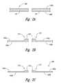
- FIGS. 2A-2Fillustrate a representative process for forming a leadframe 140 , such as the one shown in FIG. 1 .
- FIG. 2Aillustrates the central portion of the leadframe 140 , including leadfingers 141 that extend inwardly toward each other from a surrounding frame (described later with reference to FIG. 2F ).
- Each leadfinger 141can include a first leadfinger surface 142 a and a second leadfinger surface 142 b facing opposite from the first leadfinger surface 142 a.
- FIG. 2Billustrates a process for forming the second package bond sites 113 at the leadfingers 141 .
- the second package bond sites 113are formed by etching or otherwise removing material from the first leadfinger surface 142 a so as to leave projections having a bonding surface 143 that is generally parallel to the recessed first leadfinger surface 142 a, but offset away from the first leadfinger surface 142 a.
- the first leadfinger surface 142 ais located generally in a leadfinger plane, and the bonding surface 143 is offset outwardly away from the leadfinger plane.
- the bonding surface 143is generally flat, but it can have other shapes in other embodiments. In FIG.
- materialcan be removed from the first leadfinger surface 142 a, the second leadfinger surface 142 b, and/or the bonding surfaces 143 to reduce the overall thickness of the leadframe 140 .
- an adhesive 144is attached to the second leadfinger surface 142 b in preparation for bonding the leadframe 140 to a corresponding microelectronic die.
- FIG. 2Eis a cross-sectional side elevation view of an entire leadframe 140 , with an adhesive 144 attached, taken substantially along line 2 E- 2 E of FIG. 2F .
- the leadframe 140can include a frame 145 from which the leadfingers 141 extend.
- Each leadfinger 141has a single second package bond site 113 , but adjacent leadfingers 141 have different lengths and are offset relative to each other to properly align neighboring second package bond sites 113 .
- the leadfingers 141can also be bent as shown in FIG. 2E so as to fit over a corresponding microelectronic die, with the frame 145 holding the leadfingers 141 in place during the attachment process.
- the leadframe 140is generally self-supporting.
- the leadframe 140is relatively thin and flexible, it can keep its shape, and is therefore different than typical internal redistribution layers, which are formed directly on or in a microelectronic die or support member using a deposition process.
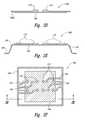
- FIGS. 3A-3Gillustrate a process for attaching the leadframe 140 to a microelectronic die 120 , and completing the formation of the resulting package.
- a microelectronic die 120is attached to the support member 130 so that the die bond sites 121 are aligned with an aperture in the support member 130 .
- Wirebonds 122are then connected between the die bond sites 121 and the support member bond sites 133 .
- the support member bond sites 133are in electrical communication with the leadframe bond sites 132 , as discussed above with reference to FIG. 1 .
- Each of the leadframe bond sites 132can optionally include a solder ball 134 or other arrangement for attaching to the leadframe and providing electrical signals to the leadframe.
- FIG. 3Billustrates the leadframe 140 positioned over the microelectronic die 120 in preparation for attaching it to both the support member 130 and the microelectronic die 120 .
- the microelectronic diehas a first surface 125 facing toward the support member 130 , and a second surface 126 facing toward the leadframe 140 .
- the leadframe 140can be attached to the microelectronic die 120 with the adhesive 144 , and the leadframe 140 can be attached and electrically coupled to the support member 130 via the solder balls 134 . Accordingly, unlike many existing applications of leadframes, the illustrated leadframe 140 does not have wirebonds attached to it.
- a suitable reflow process and/or curing processcan be used to form the foregoing attachments to the leadframe 140 .
- the reflowed solder balls 134 and cured adhesive 144are not shown in the following figures.
- FIGS. 3Cis a partially schematic, cross-sectional side view of the support member 130 and the leadframe 140 , as the outer frame 145 of the leadframe 140 is separated from the rest of the leadframe 140 along trim lines 146 .
- FIG. 3Dis a plan view of the arrangement shown in FIG. 3C .
- the leadframe 140 , the support member 130 , and the microelectronic die 120can be encapsulated, as shown in FIG. 3E .
- the support member 130with the microelectronic die 120 and the leadframe 140 attached, is placed in a mold and the encapsulant 111 is injected in the mold so as to cover the second package bond sites 113 .
- the portion of the encapsulant 111 covering the second package bond sites 113can then be removed to expose the second package bond sites 113 .
- a grinding process, laser removal process, or other appropriate processcan be used to remove the encapsulant 111 down to a removal line 115 .
- the encapsulant 111can be removed from across the entirety of the upper surface of the package, or it can be selectively removed from just the second package bond sites 113 , for example, to form “wells” that contain the solder balls or other electrical couplers that are later placed at the second package bond sites 113 .
- the step of removing the portion of the encapsulant 111 overlying the second package bond sites 113can be eliminated by preventing the encapsulant 111 from being disposed on the second package bond sites 113 in the first place.
- the mold in which the first package 110 a is placed during the encapsulation processcan include pins or other removable structures that cover over the second package bond sites 113 and prevent the encapsulant 111 from contacting and adhering to the second package bond sites 113 .
- the overlying encapsulant 111need not be removed.
- FIG. 3Gillustrates both the first package 110 a and the second package 110 b described above with reference to FIG. 1 .
- Solder balls 101have been attached to the first package bond sites 112 of each package 110 a, 110 b.
- each packagePrior to attaching the packages 110 a, 110 b to each other, each package can be separately tested using a probe 102 (shown schematically in FIG. 3G ) or another device that communicates with the internal microelectronic die 120 via the first package bond sites 112 and/or the second package bond sites 113 .
- a probe 102shown schematically in FIG. 3G
- another devicethat communicates with the internal microelectronic die 120 via the first package bond sites 112 and/or the second package bond sites 113 .
- each of the packages 110 a, 110 bcan be electronically tested prior to the stacking operation.
- An advantage of this arrangementis that the likelihood for stacking a “bad die” with a “good die” is reduced or eliminated. Accordingly, the process of stack
- the process for stacking the packages 110 a, 110 bcan include placing the second package 110 b on the first package 110 a, with the first package bond sites 112 of the second package 110 b aligned with the second package bond sites 113 of the first package 110 a.
- a reflow operationcan be used to connect the solder between the two sets of package bond sites 112 , 113 .
- each package 110can include a single support member 130 , and an arrangement of stacked packages can include as many support members as there are packages 110 . This is unlike some existing arrangements for stacking microelectronic dies, in which additional support members are used to provide the interconnections between stacked dies. Unlike these arrangements, embodiments such as those described above with reference to FIGS. 1-3G have no support member positioned between the leadframe and the microelectronic die within a given package.
- An advantage of reducing the number of support members included in the package (or package stack)is that it can reduce the overall thickness of the stack and therefore the volume occupied by the stack when it is installed in a product (e.g., a computer, cell phone, video device, etc.).
- a producte.g., a computer, cell phone, video device, etc.
- FIGS. 1-3GAnother feature of at least some of the embodiments described above with reference to FIGS. 1-3G is that they can include leadfingers 141 having bonding surfaces that project away or are offset from the parallel leadfinger surface that faces in the same direction (e.g., the first leadfinger surface 142 a shown in FIG. 2B ).
- This arrangementallows the leadfingers 141 (and in particular, the second package bond sites 113 ) to be accessible from the surface of the package that faces opposite the first package bond sites 112 .
- the packagesmay be readily stacked on one another.
- each packagehas a volume of encapsulant that is separate from and not integrated with the encapsulant of the other. Accordingly, the packages can be attached to each other and, if necessary, separated from each other at the junctions between the first package bond sites of one package and the second package bond site of the other. This feature allows the packages to be separated (for example, if one package fails), without having to disturb the encapsulant of either package.
- FIGS. 4-8illustrate packages with microelectronic dies and encapsulated leadframes configured in accordance with further embodiments of the invention.
- FIG. 4illustrates a package 410 that includes a microelectronic die 420 carried by a support member 430 having support member bond sites 433 .
- die bond sites 421 of the microelectronic die 420face away from the support member bond sites 433 and are connected to the support member bond sites 433 with wire bonds 422 that do not extend through an opening in the support member 430 .
- the package 410also includes a leadframe 440 having leadfingers 441 that extend not only over the die 420 , but also over the wirebonds 422 .
- the support member 430can include support member circuitry 431 that couples the support member bond sites 433 to first package bond sites 412 and to leadframe bond sites 432 .
- the leadframe 440can carry second package bond sites 413 that are accessible through a surrounding body of encapsulant 411 for electrical coupling to the package 410 .
- FIG. 5is a top plan view of a package 510 having an arrangement somewhat similar to that described above with reference to FIG. 4 , but with the wirebonds oriented in a different direction from, and not directly underneath, the leadfingers.
- the package 510can include a support member 530 carrying a microelectronic die 520 having die bond sites 521 positioned toward the ends of the die 520 and connected to support member bond sites 533 positioned toward the ends of the corresponding support member 530 .
- the support member bond sites 533are connected to leadframe bond sites 532 with internal circuitry (not shown) within the support member 530 .
- the leadframe 540can include leadfingers 541 that are electrically bonded to the leadframe bond sites 532 , and that extend over the orthogonally located sides of the die 520 , so as not to pass directly over the wirebonds 522 .
- the leadfingers 541can include second package bond sites 513 that are accessible for coupling in a manner generally similar to that described above. Orienting the leadfingers 541 away from the wirebonds 522 avoids physical interference between these elements, and can also reduce or eliminate electrical interference between these elements.
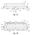
- FIG. 6illustrates a package 610 that includes a support member 630 carrying a die 620 that is electrically coupled to the support member 630 via solder balls 601 .
- the die 620can include die bond sites or bond pads 621 that face toward corresponding support member bond sites 633 , with the solder balls 601 positioned in between. Some of the die bond sites 621 and support member bond sites 633 may be offset from the plane of FIG. 6 and therefore not visible.
- the support member bond sites 633can be coupled to first package bond sites 612 and leadframe bond sites 632 in a manner generally similar to that described above.
- a leadframe 640can be attached to the leadframe bond site 632 and can carry second package bond sites 613 positioned to face in a direction opposite that of the first package bond sites 612 , also in a manner generally similar to that described above.
- FIG. 7is a partially schematic, cross-sectional side view of a package 710 that includes multiple microelectronic dies positioned within the same volume of encapsulant, and electrically coupled to the same leadframe 740 .
- the package 710can include two microelectronic dies 720 , shown as a first microelectronic die 720 a and a second microelectronic die 720 b, stacked one upon the other, with the second microelectronic die 720 b positioned between the first die 720 a and a support member 730 .
- the second microelectronic die 720 bcan include die bond sites 721 b that are electrically coupled to the support member 730 in a manner generally similar to that described above with reference to FIG. 6 .
- the first microelectronic die 720 acan include die bond sites 721 a that are electrically coupled to the support member 730 in a manner generally similar to that described above with reference to either FIG. 4 or FIG. 5 .
- the internal circuitry within the support member 730can couple first support member bond sites 733 a and second support member bond site 733 b to first package bond sites 712 and to leadframe bond sites 732 .
- a leadframe 740 having second package bond sites 713is electrically connected to the leadframe bond sites 732 and extends over the composite of the first microelectronic die 720 a and the second microelectronic die 720 b. Accordingly, an advantage of an arrangement shown in FIG. 7 is that the overall thickness of the composite may be less than the thickness of the stacked die arrangement shown in FIG. 1 . Conversely, an advantage of an embodiment shown in FIG. 1 is that each microelectronic die can be individually tested prior to stacking the packages shown in the manner as shown in FIG. 1 .
- FIG. 8is a partially schematic, cross-sectional side view of a package 810 having first and second microelectronic dies 820 a, 820 b arranged in generally the opposite fashion from that shown in FIG. 7 .
- the second die 820 bcan be connected to the corresponding support member 830 with wire bonds 822
- the first die 820 acan be coupled to the second die 820 b with solder balls 801 .
- the second die 820 bcan include second die bond sites 821 b and redistribution lines 823 that connect the second die bond sites 821 b with intermediate bond sites 824 .
- the first die 820 acan be connected directly to the second die bond sites 821 b with the solder balls 801
- the second die 820 bcan be connected to the support member 830 with wire bonds 822 connected between the intermediate bond sites 824 and corresponding support member bond sites 833
- the support member bond sites 833can be coupled to first package bond sites 812 and leadframe bond sites 832 via support member circuitry 831 .
- the leadframe bond sites 832are in turn connected to second package bond sites 813 via a corresponding leadframe 840 .
- the microelectronic diescan have configurations other than those shown in the Figures and/or can be combined in manners other than those shown in the Figures.
- the upper packagemay have no second package bond sites, a different leadframe arrangement than that of the lower package, or no leadframe at all.
- the bond sites, electrical couplers and circuitrycan be arranged and/or combined in manners other than those discussed above and shown in the Figures.
Landscapes
- Engineering & Computer Science (AREA)
- Microelectronics & Electronic Packaging (AREA)
- Power Engineering (AREA)
- Physics & Mathematics (AREA)
- Condensed Matter Physics & Semiconductors (AREA)
- General Physics & Mathematics (AREA)
- Computer Hardware Design (AREA)
- Lead Frames For Integrated Circuits (AREA)
Abstract
Description
- This application is a divisional of U.S. application Ser. No. 11/509,291 filed Aug. 23, 2006, which claims foreign priority benefits of Singapore Application No. 200604777-3 filed Jul. 17, 2006, both of which are incorporated herein by reference.
- The present disclosure is directed generally to microelectronic packages with leadframes, including leadframes configured for stacked die packages, and associated systems and methods.
- Packaged microelectronic assemblies, such as memory chips and microprocessor chips, typically include a microelectronic die mounted to a substrate and encased in a plastic protective covering. The die includes functional features, such as memory cells, processor circuits and interconnecting circuitry. The die also typically includes bond pads electrically coupled to the functional features. The bond pads are electrically connected to pins or other types of terminals that extend outside the protective covering for connecting the die to busses, circuits, and/or other microelectronic assemblies.
- In one conventional arrangement, the die is mounted to a supporting substrate (e.g., a printed circuit board), and the die bond pads are electrically coupled to corresponding bond pads of the substrate with wirebonds. After encapsulation, the substrate can be electrically connected to external devices with solder balls or other suitable connections. Accordingly, the substrate supports the die and provides an electrical link between the die and the external devices.
- In other conventional arrangements, the die can be mounted to a leadframe that has conductive leadfingers connected to a removable frame. The frame temporarily supports the leadfingers in position relative to the die during manufacture. Each leadfinger is wirebonded to a corresponding bond pad of a die, and the assembly is encapsulated in such a way that the frame and a portion of each of the leadfingers extends outside the encapsulating material. The frame is then trimmed off, and the exposed portions of each leadfinger can be bent to form pins for connecting the die to external components.
- Die manufacturers have come under increasing pressure to reduce the size of their dies and the volume occupied by the dies, and to increase the capacity of the resulting encapsulated assemblies. One approach to addressing these issues has been to stack multiple dies on top of each other so as to make increased use of the limited surface area on the circuit board or other element to which the dies are mounted. One drawback with some of the existing stacking techniques is that one of the dies may fail during a following-on test process. When this occurs, the entire package, including operational dies, is typically discarded because it is not practical to replace a single die within a package. Another potential drawback is that the stacked dies can occupy a significant volume in a vertical direction, which can in some cases reduce the benefits associated with stacking the dies. Accordingly, there is a need for techniques that reduce the thickness of stacked die packages, and improve the reliability of such packages.
FIG. 1 is a partially schematic, cross-sectional side view of a system that includes microelectronic die packages configured and stacked in accordance with an embodiment of the invention.FIGS. 2A-2F illustrate a process for forming a leadframe in accordance with an embodiment of the invention.FIGS. 3A-3G illustrate a process for encapsulating a microelectronic die and a leadframe in accordance with an embodiment of the invention.FIG. 4 is a partially schematic, cross-sectional side view of a package having a microelectronic die and leadframe configured in accordance with another embodiment of the invention.FIG. 5 is a partially schematic, top plan view of a microelectronic die carried by a support member and connected to a leadframe in accordance with another embodiment of the invention.FIG. 6 is a partially schematic, cross-sectional side view of a package that includes a microelectronic die coupled to a support member with a leadframe and solder balls in accordance with another embodiment of the invention.FIG. 7 is a partially schematic, cross-sectional side view of a package that includes two stacked microelectronic dies electrically coupled to a leadframe in accordance with another embodiment of the invention.FIG. 8 is a partially schematic, cross-sectional side view of a package that includes two stacked microelectronic dies coupled to a single leadframe in accordance with still another embodiment of the invention.- The present disclosure relates generally to microelectronic packages having leadframes, including leadframes configured for stacked packages, and associated systems and methods. For example, one system includes a support member having first package bond sites and leadframe bond sites that are electrically coupled to the first package bond sites. A microelectronic die carried by the support member is electrically coupled to the first package bond sites. The leadframe can be attached to the leadframe bond sites and can extend adjacent to the microelectronic die, with the microelectronic die positioned between the leadframe and the support member. The leadframe can have second package bond sites facing away from the first package bond sites. An encapsulant at least partially surrounds the leadframe and the microelectronic die, with the first and second package bond sites accessible from outside the encapsulant.
- In a further particular aspect, the support member, the microelectronic die, the leadframe and the encapsulant form a first microelectronic package, and the system can further include a second microelectronic package having a configuration generally similar to that of the first, with the second microelectronic package stacked on the first, and with the first package bond sites of the second microelectronic package electrically connected to the second package bond sites of the first microelectronic package. In yet further aspects, one or more of the packages can itself include multiple microelectronic dies positioned between the corresponding leadframe and the corresponding support member.
- Other aspects are directed to a leadframe for electrical coupling to a microelectronic die. The leadframe can include a conductive frame and a plurality of conductive leadfingers that are connected to and extend inwardly from the frame. Individual leadfingers can have a leadfinger surface that faces in a first direction and is located in a leadfinger plane. The individual leadfingers can further have an electrically conductive bond site with a bonding surface that is offset away from the leadfinger plane in the first direction. Leadfingers having such a construction can be positioned within microelectronic packages, with the offset bonding surfaces accessible from outside the encapsulant of the package, so as to permit coupling to the microelectronic die within the package.
- Further aspects are directed to methods for making a microelectronic die system. One such method can include carrying a microelectronic die with a support member having first package bond sites and leadframe bond sites that are electrically coupled to the first package bond sites. The method can further include electrically coupling the microelectronic die to the first package bond sites, and positioning the leadframe adjacent to the microelectronic die, with the microelectronic die located between the leadframe and the support member, and with second package bond sites of the leadframe facing away from the microelectronic die. The method can further include electrically connecting the leadframe to the leadframe bond sites, at least partially surrounding the leadframe and the die with an encapsulant, and allowing access to the first and second package bond sites from outside the encapsulant. Accordingly, the package can be coupled to external devices, and can be stacked to improve device density.
- In particular aspects, allowing access to the second package bond sites can include removing encapsulant adjacent to the package bond sites, grinding the encapsulant to expose the package bond sites, and/or restricting the encapsulant from being disposed adjacent to the second package bond sites. In further aspects, the support member can include a circuit board, and can be the only support member within the encapsulant.
- Many specific details of certain embodiments of the invention are set forth in the following description and in
FIGS. 1-8 to provide a thorough understanding of these embodiments. One skilled in the art, however, will understand that the present invention may have additional embodiments, and that the invention may be practiced without several of the details described below. FIG. 1 is a partially schematic, cross-sectional side view of asystem 100 that includes stacked microelectronic packages configured in accordance with an embodiment of the invention. Thesystem 100 can include multiple stacked packages110 (e.g., two packages, shown as afirst package 110aand asecond package 110b), each having a generally similar configuration. For example, each package110 can include a support member130 (e.g., a circuit board), a microelectronic die120 (e.g., a memory chip or a processor chip), and aleadframe 140 that provides for electrical connections between themicroelectronic die 120 and other devices, including, but not limited to, other stacked packages.- Referring to the
first package 110a,thesupport member 130 can both carry themicroelectronic die 120 and provide electrical communication to and from thedie 120. Accordingly, thesupport member 130 can have supportmember bond sites 133 that are electrically coupled to corresponding diebond sites 121 of the die120. In an embodiment shown inFIG. 1 ,wirebonds 122 provide the electrical coupling between thedie bond sites 121 and the supportmember bond sites 133, and in other embodiments, other electrical couplings (e.g., solder balls) form this link. Thesupport member 130 can also includeinternal circuitry 131 that connects the supportmember bond sites 133 with other bonds sites, including firstpackage bond sites 112 andleadframe bond sites 132. The firstpackage bond sites 112 provide communication to other devices external to the package110 viasolder balls 101 or other electrically conductive couplers. Some of the firstpackage bond sites 112 are located out of the plane ofFIG. 1 , as indicated by dashed lines. Theleadframe bond sites 132 provide communication to secondpackage bond sites 113 via theleadframe 140. Accordingly, thedie 120 can communicate withexternal devices 103 via the firstpackage bond sites 112 and/or the secondpackage bond sites 113. - Each package110 can include an
encapsulant 111 that surrounds and protects the internal components, including thewirebonds 122 and theleadframe 140. Theencapsulant 111 can be positioned and/or configured with the firstpackage bond sites 112 and the secondpackage bond sites 113 exposed for electrical coupling to other components. The other components can include other packages110 (e.g., when the packages110 are stacked), and/or external circuit boards, and/or any of a wide variety of intermediate and/or end-user devices, such as computing devices, communication devices, testing devices or other electronic components. - Stacked packages can, but need not have generally similar configurations. For example, as shown in
FIG. 1 , the twopackages second package 110bcan have itsencapsulant 111 arranged so as to cover over the secondpackage bond sites 113. Accordingly, thesecond package 110bcan be located at the top of a stack of packages (as shown inFIG. 1 ), or it can be used singly. In other embodiments, thesecond package 110bcan have an encapsulant arranged identically to that shown for thefirst package 110a,but can include an optional covering114 (shown in dashed lines inFIG. 1 ) to protect the otherwise exposedsecond bond sites 113. In still further embodiments, thesystem 100 can include dissimilar packages stacked on top of each other. FIGS. 2A-2F illustrate a representative process for forming aleadframe 140, such as the one shown inFIG. 1 .FIG. 2A illustrates the central portion of theleadframe 140, includingleadfingers 141 that extend inwardly toward each other from a surrounding frame (described later with reference toFIG. 2F ). Eachleadfinger 141 can include afirst leadfinger surface 142aand asecond leadfinger surface 142bfacing opposite from thefirst leadfinger surface 142a.FIG. 2B illustrates a process for forming the secondpackage bond sites 113 at theleadfingers 141. In one aspect of this embodiment, the secondpackage bond sites 113 are formed by etching or otherwise removing material from thefirst leadfinger surface 142aso as to leave projections having abonding surface 143 that is generally parallel to the recessedfirst leadfinger surface 142a,but offset away from thefirst leadfinger surface 142a.Accordingly, thefirst leadfinger surface 142ais located generally in a leadfinger plane, and thebonding surface 143 is offset outwardly away from the leadfinger plane. In a particular embodiment, thebonding surface 143 is generally flat, but it can have other shapes in other embodiments. InFIG. 2C , material can be removed from thefirst leadfinger surface 142a,thesecond leadfinger surface 142b,and/or the bonding surfaces143 to reduce the overall thickness of theleadframe 140. InFIG. 2D , an adhesive144 is attached to thesecond leadfinger surface 142bin preparation for bonding theleadframe 140 to a corresponding microelectronic die.FIG. 2E is a cross-sectional side elevation view of anentire leadframe 140, with an adhesive144 attached, taken substantially alongline 2E-2E ofFIG. 2F . Referring toFIGS. 2E and 2F , theleadframe 140 can include aframe 145 from which theleadfingers 141 extend. Eachleadfinger 141 has a single secondpackage bond site 113, butadjacent leadfingers 141 have different lengths and are offset relative to each other to properly align neighboring secondpackage bond sites 113. Theleadfingers 141 can also be bent as shown inFIG. 2E so as to fit over a corresponding microelectronic die, with theframe 145 holding theleadfingers 141 in place during the attachment process. In a representative embodiment, theleadframe 140 is generally self-supporting. For example, although it is relatively thin and flexible, it can keep its shape, and is therefore different than typical internal redistribution layers, which are formed directly on or in a microelectronic die or support member using a deposition process.FIGS. 3A-3G illustrate a process for attaching theleadframe 140 to amicroelectronic die 120, and completing the formation of the resulting package. Beginning withFIG. 3A , amicroelectronic die 120 is attached to thesupport member 130 so that thedie bond sites 121 are aligned with an aperture in thesupport member 130.Wirebonds 122 are then connected between thedie bond sites 121 and the supportmember bond sites 133. The supportmember bond sites 133 are in electrical communication with theleadframe bond sites 132, as discussed above with reference toFIG. 1 . Each of theleadframe bond sites 132 can optionally include asolder ball 134 or other arrangement for attaching to the leadframe and providing electrical signals to the leadframe.FIG. 3B illustrates theleadframe 140 positioned over the microelectronic die120 in preparation for attaching it to both thesupport member 130 and themicroelectronic die 120. The microelectronic die has afirst surface 125 facing toward thesupport member 130, and asecond surface 126 facing toward theleadframe 140. Theleadframe 140 can be attached to the microelectronic die120 with the adhesive144, and theleadframe 140 can be attached and electrically coupled to thesupport member 130 via thesolder balls 134. Accordingly, unlike many existing applications of leadframes, the illustratedleadframe 140 does not have wirebonds attached to it. A suitable reflow process and/or curing process can be used to form the foregoing attachments to theleadframe 140. For purposes of illustration, the reflowedsolder balls 134 and cured adhesive144 are not shown in the following figures.FIGS. 3C is a partially schematic, cross-sectional side view of thesupport member 130 and theleadframe 140, as theouter frame 145 of theleadframe 140 is separated from the rest of theleadframe 140 alongtrim lines 146.FIG. 3D is a plan view of the arrangement shown inFIG. 3C . Once theouter frame 145 has been separated, theleadframe 140, thesupport member 130, and the microelectronic die120 can be encapsulated, as shown inFIG. 3E . In a particular aspect of this arrangement, thesupport member 130, with themicroelectronic die 120 and theleadframe 140 attached, is placed in a mold and theencapsulant 111 is injected in the mold so as to cover the secondpackage bond sites 113. As shown inFIG. 3F , the portion of theencapsulant 111 covering the secondpackage bond sites 113 can then be removed to expose the secondpackage bond sites 113. For example, a grinding process, laser removal process, or other appropriate process can be used to remove theencapsulant 111 down to aremoval line 115. Theencapsulant 111 can be removed from across the entirety of the upper surface of the package, or it can be selectively removed from just the secondpackage bond sites 113, for example, to form “wells” that contain the solder balls or other electrical couplers that are later placed at the secondpackage bond sites 113.- In another arrangement, the step of removing the portion of the
encapsulant 111 overlying the secondpackage bond sites 113 can be eliminated by preventing the encapsulant111 from being disposed on the secondpackage bond sites 113 in the first place. For example, the mold in which thefirst package 110ais placed during the encapsulation process can include pins or other removable structures that cover over the secondpackage bond sites 113 and prevent the encapsulant111 from contacting and adhering to the secondpackage bond sites 113. Also, as discussed above with reference toFIG. 1 , if the particular package need not have the secondpackage bond sites 113 exposed (e.g., if the package is intended to be placed at the top of a package stack), then theoverlying encapsulant 111 need not be removed. FIG. 3G illustrates both thefirst package 110aand thesecond package 110bdescribed above with reference toFIG. 1 .Solder balls 101 have been attached to the firstpackage bond sites 112 of eachpackage packages FIG. 3G ) or another device that communicates with the internal microelectronic die120 via the firstpackage bond sites 112 and/or the secondpackage bond sites 113. In this manner, each of thepackages packages - The process for stacking the
packages second package 110bon thefirst package 110a,with the firstpackage bond sites 112 of thesecond package 110baligned with the secondpackage bond sites 113 of thefirst package 110a.Whensolder balls 101 are used to connect thepackages package bond sites - One feature of at least some of the embodiments described above with reference to
FIGS. 1-3G is that each package110 can include asingle support member 130, and an arrangement of stacked packages can include as many support members as there are packages110. This is unlike some existing arrangements for stacking microelectronic dies, in which additional support members are used to provide the interconnections between stacked dies. Unlike these arrangements, embodiments such as those described above with reference toFIGS. 1-3G have no support member positioned between the leadframe and the microelectronic die within a given package. An advantage of reducing the number of support members included in the package (or package stack) is that it can reduce the overall thickness of the stack and therefore the volume occupied by the stack when it is installed in a product (e.g., a computer, cell phone, video device, etc.). - Another feature of at least some of the embodiments described above with reference to
FIGS. 1-3G is that they can includeleadfingers 141 having bonding surfaces that project away or are offset from the parallel leadfinger surface that faces in the same direction (e.g., thefirst leadfinger surface 142ashown inFIG. 2B ). This arrangement allows the leadfingers141 (and in particular, the second package bond sites113) to be accessible from the surface of the package that faces opposite the firstpackage bond sites 112. As a result, the packages may be readily stacked on one another. - Another feature of at least some of the embodiments described above with reference to
FIGS. 1-3G is that each package has a volume of encapsulant that is separate from and not integrated with the encapsulant of the other. Accordingly, the packages can be attached to each other and, if necessary, separated from each other at the junctions between the first package bond sites of one package and the second package bond site of the other. This feature allows the packages to be separated (for example, if one package fails), without having to disturb the encapsulant of either package. FIGS. 4-8 illustrate packages with microelectronic dies and encapsulated leadframes configured in accordance with further embodiments of the invention. For example,FIG. 4 illustrates apackage 410 that includes amicroelectronic die 420 carried by asupport member 430 having supportmember bond sites 433. Unlike the arrangement shown inFIG. 1 , diebond sites 421 of themicroelectronic die 420 face away from the supportmember bond sites 433 and are connected to the supportmember bond sites 433 withwire bonds 422 that do not extend through an opening in thesupport member 430. Thepackage 410 also includes aleadframe 440 havingleadfingers 441 that extend not only over thedie 420, but also over the wirebonds422. Other aspects of thepackage 410 can be generally similar to those described above with reference toFIG. 1 . For example, thesupport member 430 can includesupport member circuitry 431 that couples the supportmember bond sites 433 to firstpackage bond sites 412 and to leadframebond sites 432. Theleadframe 440 can carry secondpackage bond sites 413 that are accessible through a surrounding body ofencapsulant 411 for electrical coupling to thepackage 410.FIG. 5 is a top plan view of apackage 510 having an arrangement somewhat similar to that described above with reference toFIG. 4 , but with the wirebonds oriented in a different direction from, and not directly underneath, the leadfingers. For example, thepackage 510 can include asupport member 530 carrying amicroelectronic die 520 havingdie bond sites 521 positioned toward the ends of thedie 520 and connected to supportmember bond sites 533 positioned toward the ends of thecorresponding support member 530. The supportmember bond sites 533 are connected to leadframebond sites 532 with internal circuitry (not shown) within thesupport member 530. Theleadframe 540 can includeleadfingers 541 that are electrically bonded to theleadframe bond sites 532, and that extend over the orthogonally located sides of thedie 520, so as not to pass directly over the wirebonds522. Theleadfingers 541 can include secondpackage bond sites 513 that are accessible for coupling in a manner generally similar to that described above. Orienting theleadfingers 541 away from thewirebonds 522 avoids physical interference between these elements, and can also reduce or eliminate electrical interference between these elements.FIG. 6 illustrates apackage 610 that includes asupport member 630 carrying adie 620 that is electrically coupled to thesupport member 630 viasolder balls 601. Accordingly, thedie 620 can include die bond sites orbond pads 621 that face toward corresponding supportmember bond sites 633, with thesolder balls 601 positioned in between. Some of thedie bond sites 621 and supportmember bond sites 633 may be offset from the plane ofFIG. 6 and therefore not visible. The supportmember bond sites 633 can be coupled to firstpackage bond sites 612 andleadframe bond sites 632 in a manner generally similar to that described above. Aleadframe 640 can be attached to theleadframe bond site 632 and can carry secondpackage bond sites 613 positioned to face in a direction opposite that of the firstpackage bond sites 612, also in a manner generally similar to that described above.FIG. 7 is a partially schematic, cross-sectional side view of apackage 710 that includes multiple microelectronic dies positioned within the same volume of encapsulant, and electrically coupled to thesame leadframe 740. For example, thepackage 710 can include two microelectronic dies720, shown as a first microelectronic die720aand a second microelectronic die720b,stacked one upon the other, with the second microelectronic die720bpositioned between thefirst die 720aand asupport member 730. The second microelectronic die720bcan include diebond sites 721bthat are electrically coupled to thesupport member 730 in a manner generally similar to that described above with reference toFIG. 6 . The first microelectronic die720acan include diebond sites 721athat are electrically coupled to thesupport member 730 in a manner generally similar to that described above with reference to eitherFIG. 4 orFIG. 5 . The internal circuitry within thesupport member 730 can couple first supportmember bond sites 733aand second supportmember bond site 733bto firstpackage bond sites 712 and to leadframebond sites 732. Aleadframe 740 having secondpackage bond sites 713 is electrically connected to theleadframe bond sites 732 and extends over the composite of the first microelectronic die720aand the second microelectronic die720b.Accordingly, an advantage of an arrangement shown inFIG. 7 is that the overall thickness of the composite may be less than the thickness of the stacked die arrangement shown inFIG. 1 . Conversely, an advantage of an embodiment shown inFIG. 1 is that each microelectronic die can be individually tested prior to stacking the packages shown in the manner as shown inFIG. 1 .FIG. 8 is a partially schematic, cross-sectional side view of apackage 810 having first and second microelectronic dies820a,820barranged in generally the opposite fashion from that shown inFIG. 7 . Accordingly, thesecond die 820bcan be connected to thecorresponding support member 830 withwire bonds 822, and thefirst die 820acan be coupled to thesecond die 820bwithsolder balls 801. In a particular aspect of this embodiment, thesecond die 820bcan include seconddie bond sites 821bandredistribution lines 823 that connect the seconddie bond sites 821bwithintermediate bond sites 824. The first die820acan be connected directly to the seconddie bond sites 821bwith thesolder balls 801, and thesecond die 820bcan be connected to thesupport member 830 withwire bonds 822 connected between theintermediate bond sites 824 and corresponding supportmember bond sites 833. The supportmember bond sites 833 can be coupled to firstpackage bond sites 812 andleadframe bond sites 832 viasupport member circuitry 831. Theleadframe bond sites 832 are in turn connected to secondpackage bond sites 813 via a corresponding leadframe840.- From the foregoing, it will be appreciated that specific embodiments of the invention have been described herein for purposes of illustration, but that various modifications may be made without deviating from the scope of the invention. For example, the microelectronic dies can have configurations other than those shown in the Figures and/or can be combined in manners other than those shown in the Figures. In certain embodiments, when packages are stacked on each other, they need not have the same configuration. For example, the upper package may have no second package bond sites, a different leadframe arrangement than that of the lower package, or no leadframe at all. The bond sites, electrical couplers and circuitry can be arranged and/or combined in manners other than those discussed above and shown in the Figures. Although advantages associated with certain embodiments of the invention have been described in the context of those embodiments, other embodiments may also exhibit such advantages. Additionally, none of the foregoing embodiments need necessarily exhibit such advantages to fall within the scope of the invention. Accordingly, the invention is not limited except as by the appended claims.
Claims (27)
Priority Applications (2)
| Application Number | Priority Date | Filing Date | Title |
|---|---|---|---|
| US12/726,130US8869387B2 (en) | 2006-07-17 | 2010-03-17 | Methods for making microelectronic die systems |
| US14/525,787US20150041204A1 (en) | 2006-07-17 | 2014-10-28 | Microelectronic packages with leadframes, including leadframes configured for stacked die packages, and associated systems and methods |
Applications Claiming Priority (4)
| Application Number | Priority Date | Filing Date | Title |
|---|---|---|---|
| SG200604777-3ASG139573A1 (en) | 2006-07-17 | 2006-07-17 | Microelectronic packages with leadframes, including leadframes configured for stacked die packages, and associated systems and methods |
| SG200604777-3 | 2006-07-17 | ||
| US11/509,291US7692931B2 (en) | 2006-07-17 | 2006-08-23 | Microelectronic packages with leadframes, including leadframes configured for stacked die packages, and associated systems and methods |
| US12/726,130US8869387B2 (en) | 2006-07-17 | 2010-03-17 | Methods for making microelectronic die systems |
Related Parent Applications (1)
| Application Number | Title | Priority Date | Filing Date |
|---|---|---|---|
| US11/509,291DivisionUS7692931B2 (en) | 2006-07-17 | 2006-08-23 | Microelectronic packages with leadframes, including leadframes configured for stacked die packages, and associated systems and methods |
Related Child Applications (1)
| Application Number | Title | Priority Date | Filing Date |
|---|---|---|---|
| US14/525,787DivisionUS20150041204A1 (en) | 2006-07-17 | 2014-10-28 | Microelectronic packages with leadframes, including leadframes configured for stacked die packages, and associated systems and methods |
Publications (2)
| Publication Number | Publication Date |
|---|---|
| US20100173454A1true US20100173454A1 (en) | 2010-07-08 |
| US8869387B2 US8869387B2 (en) | 2014-10-28 |
Family
ID=38948406
Family Applications (3)
| Application Number | Title | Priority Date | Filing Date |
|---|---|---|---|
| US11/509,291Active2027-05-03US7692931B2 (en) | 2006-07-17 | 2006-08-23 | Microelectronic packages with leadframes, including leadframes configured for stacked die packages, and associated systems and methods |
| US12/726,130Active2029-10-03US8869387B2 (en) | 2006-07-17 | 2010-03-17 | Methods for making microelectronic die systems |
| US14/525,787AbandonedUS20150041204A1 (en) | 2006-07-17 | 2014-10-28 | Microelectronic packages with leadframes, including leadframes configured for stacked die packages, and associated systems and methods |
Family Applications Before (1)
| Application Number | Title | Priority Date | Filing Date |
|---|---|---|---|
| US11/509,291Active2027-05-03US7692931B2 (en) | 2006-07-17 | 2006-08-23 | Microelectronic packages with leadframes, including leadframes configured for stacked die packages, and associated systems and methods |
Family Applications After (1)
| Application Number | Title | Priority Date | Filing Date |
|---|---|---|---|
| US14/525,787AbandonedUS20150041204A1 (en) | 2006-07-17 | 2014-10-28 | Microelectronic packages with leadframes, including leadframes configured for stacked die packages, and associated systems and methods |
Country Status (2)
| Country | Link |
|---|---|
| US (3) | US7692931B2 (en) |
| SG (1) | SG139573A1 (en) |
Cited By (2)
| Publication number | Priority date | Publication date | Assignee | Title |
|---|---|---|---|---|
| US20110316156A1 (en)* | 2010-06-24 | 2011-12-29 | Stats Chippac, Ltd. | Semiconductor Device and Method of Forming RDL Along Sloped Side Surface of Semiconductor Die for Z-Direction Interconnect |
| US20130181332A1 (en)* | 2012-01-18 | 2013-07-18 | Intersil Americas LLC | Package leadframe for dual side assembly |
Families Citing this family (63)
| Publication number | Priority date | Publication date | Assignee | Title |
|---|---|---|---|---|
| SG130055A1 (en) | 2005-08-19 | 2007-03-20 | Micron Technology Inc | Microelectronic devices, stacked microelectronic devices, and methods for manufacturing microelectronic devices |
| SG130066A1 (en) | 2005-08-26 | 2007-03-20 | Micron Technology Inc | Microelectronic device packages, stacked microelectronic device packages, and methods for manufacturing microelectronic devices |
| SG139573A1 (en) | 2006-07-17 | 2008-02-29 | Micron Technology Inc | Microelectronic packages with leadframes, including leadframes configured for stacked die packages, and associated systems and methods |
| SG149726A1 (en)* | 2007-07-24 | 2009-02-27 | Micron Technology Inc | Microelectronic die packages with metal leads, including metal leads for stacked die packages, and associated systems and methods |
| US7838978B2 (en)* | 2007-09-19 | 2010-11-23 | Infineon Technologies Ag | Semiconductor device |
| US8120186B2 (en)* | 2008-02-15 | 2012-02-21 | Qimonda Ag | Integrated circuit and method |
| US7832278B2 (en)* | 2008-05-29 | 2010-11-16 | Hong Kong Applied Science And Technology Research Institute Co., Ltd. | Multi-chip package |
| US7969018B2 (en)* | 2008-07-15 | 2011-06-28 | Infineon Technologies Ag | Stacked semiconductor chips with separate encapsulations |
| US7612436B1 (en) | 2008-07-31 | 2009-11-03 | Micron Technology, Inc. | Packaged microelectronic devices with a lead frame |
| US7843047B2 (en)* | 2008-11-21 | 2010-11-30 | Stats Chippac Ltd. | Encapsulant interposer system with integrated passive devices and manufacturing method therefor |
| CN102576701B (en)* | 2009-09-02 | 2016-08-17 | 凯信公司 | IC package and method of manufacturing the same |
| US8482111B2 (en) | 2010-07-19 | 2013-07-09 | Tessera, Inc. | Stackable molded microelectronic packages |
| JP4996729B2 (en)* | 2010-09-15 | 2012-08-08 | 株式会社東芝 | Electronics and board assembly |
| KR101128063B1 (en) | 2011-05-03 | 2012-04-23 | 테세라, 인코포레이티드 | Package-on-package assembly with wire bonds to encapsulation surface |
| US11830845B2 (en) | 2011-05-03 | 2023-11-28 | Tessera Llc | Package-on-package assembly with wire bonds to encapsulation surface |
| US8513817B2 (en) | 2011-07-12 | 2013-08-20 | Invensas Corporation | Memory module in a package |
| US8502390B2 (en) | 2011-07-12 | 2013-08-06 | Tessera, Inc. | De-skewed multi-die packages |
| US8823165B2 (en) | 2011-07-12 | 2014-09-02 | Invensas Corporation | Memory module in a package |
| US8441111B2 (en) | 2011-10-03 | 2013-05-14 | Invensas Corporation | Stub minimization for multi-die wirebond assemblies with parallel windows |
| JP5947904B2 (en) | 2011-10-03 | 2016-07-06 | インヴェンサス・コーポレイション | Stub minimization for multi-die wirebond assemblies with orthogonal windows |
| US8653646B2 (en) | 2011-10-03 | 2014-02-18 | Invensas Corporation | Stub minimization using duplicate sets of terminals for wirebond assemblies without windows |
| KR101894823B1 (en) | 2011-10-03 | 2018-09-04 | 인벤사스 코포레이션 | Stub minimization for multi-die wirebond assemblies with parallel windows |
| US8436477B2 (en) | 2011-10-03 | 2013-05-07 | Invensas Corporation | Stub minimization using duplicate sets of signal terminals in assemblies without wirebonds to package substrate |
| US8405207B1 (en) | 2011-10-03 | 2013-03-26 | Invensas Corporation | Stub minimization for wirebond assemblies without windows |
| TWI515864B (en) | 2011-10-03 | 2016-01-01 | 英帆薩斯公司 | Stub minimization with terminal grids offset from center of package |
| US8345441B1 (en) | 2011-10-03 | 2013-01-01 | Invensas Corporation | Stub minimization for multi-die wirebond assemblies with parallel windows |
| US8436457B2 (en) | 2011-10-03 | 2013-05-07 | Invensas Corporation | Stub minimization for multi-die wirebond assemblies with parallel windows |
| US8525327B2 (en) | 2011-10-03 | 2013-09-03 | Invensas Corporation | Stub minimization for assemblies without wirebonds to package substrate |
| US8836136B2 (en) | 2011-10-17 | 2014-09-16 | Invensas Corporation | Package-on-package assembly with wire bond vias |
| US8835228B2 (en) | 2012-05-22 | 2014-09-16 | Invensas Corporation | Substrate-less stackable package with wire-bond interconnect |
| US9548283B2 (en)* | 2012-07-05 | 2017-01-17 | Taiwan Semiconductor Manufacturing Company, Ltd. | Package redistribution layer structure and method of forming same |
| US9136213B2 (en) | 2012-08-02 | 2015-09-15 | Infineon Technologies Ag | Integrated system and method of making the integrated system |
| US9502390B2 (en) | 2012-08-03 | 2016-11-22 | Invensas Corporation | BVA interposer |
| US9368477B2 (en) | 2012-08-27 | 2016-06-14 | Invensas Corporation | Co-support circuit panel and microelectronic packages |
| US8848391B2 (en) | 2012-08-27 | 2014-09-30 | Invensas Corporation | Co-support component and microelectronic assembly |
| US8787034B2 (en) | 2012-08-27 | 2014-07-22 | Invensas Corporation | Co-support system and microelectronic assembly |
| US8848392B2 (en) | 2012-08-27 | 2014-09-30 | Invensas Corporation | Co-support module and microelectronic assembly |
| US9070423B2 (en) | 2013-06-11 | 2015-06-30 | Invensas Corporation | Single package dual channel memory with co-support |
| US9167710B2 (en) | 2013-08-07 | 2015-10-20 | Invensas Corporation | Embedded packaging with preformed vias |
| US9123555B2 (en) | 2013-10-25 | 2015-09-01 | Invensas Corporation | Co-support for XFD packaging |
| US9583456B2 (en) | 2013-11-22 | 2017-02-28 | Invensas Corporation | Multiple bond via arrays of different wire heights on a same substrate |
| US9583411B2 (en) | 2014-01-17 | 2017-02-28 | Invensas Corporation | Fine pitch BVA using reconstituted wafer with area array accessible for testing |
| US10381326B2 (en) | 2014-05-28 | 2019-08-13 | Invensas Corporation | Structure and method for integrated circuits packaging with increased density |
| KR102337876B1 (en) | 2014-06-10 | 2021-12-10 | 삼성전자주식회사 | Semiconductor package and method of manufacturing the same |
| US9281296B2 (en) | 2014-07-31 | 2016-03-08 | Invensas Corporation | Die stacking techniques in BGA memory package for small footprint CPU and memory motherboard design |
| US9691437B2 (en) | 2014-09-25 | 2017-06-27 | Invensas Corporation | Compact microelectronic assembly having reduced spacing between controller and memory packages |
| WO2016076866A1 (en)* | 2014-11-12 | 2016-05-19 | Intel Corporation | Wearable electronic devices and components thereof |
| US9888579B2 (en) | 2015-03-05 | 2018-02-06 | Invensas Corporation | Pressing of wire bond wire tips to provide bent-over tips |
| US9502372B1 (en) | 2015-04-30 | 2016-11-22 | Invensas Corporation | Wafer-level packaging using wire bond wires in place of a redistribution layer |
| US10490528B2 (en) | 2015-10-12 | 2019-11-26 | Invensas Corporation | Embedded wire bond wires |
| US9490222B1 (en) | 2015-10-12 | 2016-11-08 | Invensas Corporation | Wire bond wires for interference shielding |
| US10332854B2 (en) | 2015-10-23 | 2019-06-25 | Invensas Corporation | Anchoring structure of fine pitch bva |
| US10181457B2 (en) | 2015-10-26 | 2019-01-15 | Invensas Corporation | Microelectronic package for wafer-level chip scale packaging with fan-out |
| US9484080B1 (en) | 2015-11-09 | 2016-11-01 | Invensas Corporation | High-bandwidth memory application with controlled impedance loading |
| US10043779B2 (en) | 2015-11-17 | 2018-08-07 | Invensas Corporation | Packaged microelectronic device for a package-on-package device |
| US9984992B2 (en) | 2015-12-30 | 2018-05-29 | Invensas Corporation | Embedded wire bond wires for vertical integration with separate surface mount and wire bond mounting surfaces |
| US9679613B1 (en) | 2016-05-06 | 2017-06-13 | Invensas Corporation | TFD I/O partition for high-speed, high-density applications |
| US10319396B2 (en) | 2016-06-16 | 2019-06-11 | Seagate Technology Llc | Transducer bar translation system and method of translating a transducer bar |
| US9935075B2 (en) | 2016-07-29 | 2018-04-03 | Invensas Corporation | Wire bonding method and apparatus for electromagnetic interference shielding |
| US10299368B2 (en) | 2016-12-21 | 2019-05-21 | Invensas Corporation | Surface integrated waveguides and circuit structures therefor |
| JP6640780B2 (en)* | 2017-03-22 | 2020-02-05 | キオクシア株式会社 | Semiconductor device manufacturing method and semiconductor device |
| KR20230011643A (en) | 2021-07-14 | 2023-01-25 | 삼성전자주식회사 | Semiconductor packages having conneting stucture |
| CN114334851A (en)* | 2021-12-27 | 2022-04-12 | 华进半导体封装先导技术研发中心有限公司 | A kind of fan-out package structure and preparation method thereof |
Citations (86)
| Publication number | Priority date | Publication date | Assignee | Title |
|---|---|---|---|---|
| US3746934A (en)* | 1971-05-06 | 1973-07-17 | Siemens Ag | Stack arrangement of semiconductor chips |
| US5107328A (en)* | 1991-02-13 | 1992-04-21 | Micron Technology, Inc. | Packaging means for a semiconductor die having particular shelf structure |
| US5128831A (en)* | 1991-10-31 | 1992-07-07 | Micron Technology, Inc. | High-density electronic package comprising stacked sub-modules which are electrically interconnected by solder-filled vias |
| US5138434A (en)* | 1991-01-22 | 1992-08-11 | Micron Technology, Inc. | Packaging for semiconductor logic devices |
| US5145099A (en)* | 1990-07-13 | 1992-09-08 | Micron Technology, Inc. | Method for combining die attach and lead bond in the assembly of a semiconductor package |
| US5252857A (en)* | 1991-08-05 | 1993-10-12 | International Business Machines Corporation | Stacked DCA memory chips |
| US5356838A (en)* | 1993-01-13 | 1994-10-18 | Samsung Electronics Co., Ltd. | Manufacturing method of a semiconductor device |
| US5518957A (en)* | 1991-10-10 | 1996-05-21 | Samsung Electronics Co., Ltd. | Method for making a thin profile semiconductor package |
| US5554886A (en)* | 1994-03-30 | 1996-09-10 | Goldstar Electron Co., Ltd. | Lead frame and semiconductor package with such lead frame |
| US5593927A (en)* | 1993-10-14 | 1997-01-14 | Micron Technology, Inc. | Method for packaging semiconductor dice |
| US5677566A (en)* | 1995-05-08 | 1997-10-14 | Micron Technology, Inc. | Semiconductor chip package |
| US5760471A (en)* | 1994-04-20 | 1998-06-02 | Fujitsu Limited | Semiconductor device having an inner lead extending over a central portion of a semiconductor device sealed in a plastic package and an outer lead exposed to the outside of a side face of the plastic package |
| US5801439A (en)* | 1994-04-20 | 1998-09-01 | Fujitsu Limited | Semiconductor device and semiconductor device unit for a stack arrangement |
| US5811877A (en)* | 1994-08-30 | 1998-09-22 | Hitachi, Ltd. | Semiconductor device structure |
| US5826628A (en)* | 1996-01-24 | 1998-10-27 | Micron Technology, Inc. | Form tooling and method of forming semiconductor package leads |
| US5835988A (en)* | 1996-03-27 | 1998-11-10 | Mitsubishi Denki Kabushiki Kaisha | Packed semiconductor device with wrap around external leads |
| US5851845A (en)* | 1995-12-18 | 1998-12-22 | Micron Technology, Inc. | Process for packaging a semiconductor die using dicing and testing |
| US5879965A (en)* | 1997-06-19 | 1999-03-09 | Micron Technology, Inc. | Plastic lead frames for semiconductor devices, packages including same, and methods of fabrication |
| US5883426A (en)* | 1996-04-18 | 1999-03-16 | Nec Corporation | Stack module |
| US5891797A (en)* | 1997-10-20 | 1999-04-06 | Micron Technology, Inc. | Method of forming a support structure for air bridge wiring of an integrated circuit |
| US5894218A (en)* | 1994-04-18 | 1999-04-13 | Micron Technology, Inc. | Method and apparatus for automatically positioning electronic dice within component packages |
| US5933713A (en)* | 1998-04-06 | 1999-08-03 | Micron Technology, Inc. | Method of forming overmolded chip scale package and resulting product |
| US5938956A (en)* | 1996-09-10 | 1999-08-17 | Micron Technology, Inc. | Circuit and method for heating an adhesive to package or rework a semiconductor die |
| US5946553A (en)* | 1991-06-04 | 1999-08-31 | Micron Technology, Inc. | Process for manufacturing a semiconductor package with bi-substrate die |
| US5986209A (en)* | 1997-07-09 | 1999-11-16 | Micron Technology, Inc. | Package stack via bottom leaded plastic (BLP) packaging |
| US5990566A (en)* | 1998-05-20 | 1999-11-23 | Micron Technology, Inc. | High density semiconductor package |
| US5994784A (en)* | 1997-12-18 | 1999-11-30 | Micron Technology, Inc. | Die positioning in integrated circuit packaging |
| US6002167A (en)* | 1995-09-22 | 1999-12-14 | Hitachi Cable, Ltd. | Semiconductor device having lead on chip structure |
| US6004867A (en)* | 1996-12-16 | 1999-12-21 | Samsung Electronics Co., Ltd. | Chip-size packages assembled using mass production techniques at the wafer-level |
| USRE36469E (en)* | 1988-09-30 | 1999-12-28 | Micron Technology, Inc. | Packaging for semiconductor logic devices |
| US6008070A (en)* | 1998-05-21 | 1999-12-28 | Micron Technology, Inc. | Wafer level fabrication and assembly of chip scale packages |
| US6018249A (en)* | 1997-12-11 | 2000-01-25 | Micron Technolgoy, Inc. | Test system with mechanical alignment for semiconductor chip scale packages and dice |
| US6020629A (en)* | 1998-06-05 | 2000-02-01 | Micron Technology, Inc. | Stacked semiconductor package and method of fabrication |
| US6028365A (en)* | 1998-03-30 | 2000-02-22 | Micron Technology, Inc. | Integrated circuit package and method of fabrication |
| US6030858A (en)* | 1996-11-22 | 2000-02-29 | Lg Semicon Co., Ltd. | Stacked bottom lead package in semiconductor devices and fabricating method thereof |
| US6048744A (en)* | 1997-09-15 | 2000-04-11 | Micron Technology, Inc. | Integrated circuit package alignment feature |
| US6051878A (en)* | 1997-03-10 | 2000-04-18 | Micron Technology, Inc. | Method of constructing stacked packages |
| US6066514A (en)* | 1996-10-18 | 2000-05-23 | Micron Technology, Inc. | Adhesion enhanced semiconductor die for mold compound packaging |
| US6072236A (en)* | 1996-03-07 | 2000-06-06 | Micron Technology, Inc. | Micromachined chip scale package |
| US6072233A (en)* | 1998-05-04 | 2000-06-06 | Micron Technology, Inc. | Stackable ball grid array package |
| US6089920A (en)* | 1998-05-04 | 2000-07-18 | Micron Technology, Inc. | Modular die sockets with flexible interconnects for packaging bare semiconductor die |
| US6097087A (en)* | 1997-10-31 | 2000-08-01 | Micron Technology, Inc. | Semiconductor package including flex circuit, interconnects and dense array external contacts |
| US6104086A (en)* | 1997-05-20 | 2000-08-15 | Nec Corporation | Semiconductor device having lead terminals bent in J-shape |
| US6103547A (en)* | 1997-01-17 | 2000-08-15 | Micron Technology, Inc. | High speed IC package configuration |
| US6107122A (en)* | 1997-08-04 | 2000-08-22 | Micron Technology, Inc. | Direct die contact (DDC) semiconductor package |
| US6111312A (en)* | 1998-08-20 | 2000-08-29 | Fujitsu Limited | Semiconductor device with leads engaged with notches |
| US6130474A (en)* | 1996-12-30 | 2000-10-10 | Micron Technology, Inc. | Leads under chip IC package |
| US6133068A (en)* | 1997-10-06 | 2000-10-17 | Micron Technology, Inc. | Increasing the gap between a lead frame and a semiconductor die |
| US6150710A (en)* | 1998-08-20 | 2000-11-21 | Micron Technology, Inc. | Transverse hybrid LOC package |
| US6148509A (en)* | 1997-04-07 | 2000-11-21 | Micron Technology, Inc. | Method for supporting an integrated circuit die |
| US6153924A (en)* | 1998-02-23 | 2000-11-28 | Micron Technology, Inc. | Multilayered lead frame for semiconductor package |
| US6159764A (en)* | 1997-07-02 | 2000-12-12 | Micron Technology, Inc. | Varied-thickness heat sink for integrated circuit (IC) packages and method of fabricating IC packages |
| US6175149B1 (en)* | 1998-02-13 | 2001-01-16 | Micron Technology, Inc. | Mounting multiple semiconductor dies in a package |
| US6184465B1 (en)* | 1998-11-12 | 2001-02-06 | Micron Technology, Inc. | Semiconductor package |
| US6187615B1 (en)* | 1998-08-28 | 2001-02-13 | Samsung Electronics Co., Ltd. | Chip scale packages and methods for manufacturing the chip scale packages at wafer level |
| US6188232B1 (en)* | 1996-12-31 | 2001-02-13 | Micron Technology, Inc. | Temporary package, system, and method for testing semiconductor dice and chip scale packages |
| US6198172B1 (en)* | 1997-02-20 | 2001-03-06 | Micron Technology, Inc. | Semiconductor chip package |
| US6201304B1 (en)* | 1995-12-19 | 2001-03-13 | Micron Technology, Inc. | Flip chip adaptor package for bare die |
| US6212767B1 (en)* | 1999-08-31 | 2001-04-10 | Micron Technology, Inc. | Assembling a stacked die package |
| US6214716B1 (en)* | 1998-09-30 | 2001-04-10 | Micron Technology, Inc. | Semiconductor substrate-based BGA interconnection and methods of farication same |
| US6225689B1 (en)* | 1998-08-21 | 2001-05-01 | Micron Technology, Inc. | Low profile multi-IC chip package connector |
| US6229202B1 (en)* | 2000-01-10 | 2001-05-08 | Micron Technology, Inc. | Semiconductor package having downset leadframe for reducing package bow |
| US6228548B1 (en)* | 1998-02-27 | 2001-05-08 | Micron Technology, Inc. | Method of making a multichip semiconductor package |
| US6228687B1 (en)* | 1999-06-28 | 2001-05-08 | Micron Technology, Inc. | Wafer-level package and methods of fabricating |
| US6232666B1 (en)* | 1998-12-04 | 2001-05-15 | Mciron Technology, Inc. | Interconnect for packaging semiconductor dice and fabricating BGA packages |
| US6235554B1 (en)* | 1995-11-27 | 2001-05-22 | Micron Technology, Inc. | Method for fabricating stackable chip scale semiconductor package |
| US6235552B1 (en)* | 1999-07-09 | 2001-05-22 | Samsung Electronics Co., Ltd. | Chip scale package and method for manufacturing the same using a redistribution substrate |
| US6239489B1 (en)* | 1999-07-30 | 2001-05-29 | Micron Technology, Inc. | Reinforcement of lead bonding in microelectronics packages |
| US6246110B1 (en)* | 1998-07-06 | 2001-06-12 | Micron Technology, Inc. | Downset lead frame for semiconductor packages |
| US6247629B1 (en)* | 1997-09-08 | 2001-06-19 | Micron Technology, Inc. | Wire bond monitoring system for layered packages |
| US6252772B1 (en)* | 1999-02-10 | 2001-06-26 | Micron Technology, Inc. | Removable heat sink bumpers on a quad flat package |
| US6261865B1 (en)* | 1998-10-06 | 2001-07-17 | Micron Technology, Inc. | Multi chip semiconductor package and method of construction |
| US6281577B1 (en)* | 1996-06-28 | 2001-08-28 | Pac Tech-Packaging Technologies Gmbh | Chips arranged in plurality of planes and electrically connected to one another |
| US6281042B1 (en)* | 1998-08-31 | 2001-08-28 | Micron Technology, Inc. | Structure and method for a high performance electronic packaging assembly |
| US6284571B1 (en)* | 1997-07-02 | 2001-09-04 | Micron Technology, Inc. | Lead frame assemblies with voltage reference plane and IC packages including same |
| US6285204B1 (en)* | 1996-03-19 | 2001-09-04 | Micron Technology, Inc. | Method for testing semiconductor packages using oxide penetrating test contacts |
| US6291894B1 (en)* | 1998-08-31 | 2001-09-18 | Micron Technology, Inc. | Method and apparatus for a semiconductor package for vertical surface mounting |
| US6294839B1 (en)* | 1999-08-30 | 2001-09-25 | Micron Technology, Inc. | Apparatus and methods of packaging and testing die |
| US6297547B1 (en)* | 1998-02-13 | 2001-10-02 | Micron Technology Inc. | Mounting multiple semiconductor dies in a package |
| US6303981B1 (en)* | 1999-09-01 | 2001-10-16 | Micron Technology, Inc. | Semiconductor package having stacked dice and leadframes and method of fabrication |
| US20030113952A1 (en)* | 2001-12-19 | 2003-06-19 | Mahesh Sambasivam | Underfill materials dispensed in a flip chip package by way of a through hole |
| US20070284715A1 (en)* | 2006-06-07 | 2007-12-13 | Advanced Semiconductor Engineering, Inc. | System-in-package device |
| US7589417B2 (en)* | 2004-02-12 | 2009-09-15 | Intel Corporation | Microelectronic assembly having thermoelectric elements to cool a die and a method of making the same |
| US7633157B2 (en)* | 2005-12-13 | 2009-12-15 | Micron Technology, Inc. | Microelectronic devices having a curved surface and methods for manufacturing the same |
| US8030098B1 (en)* | 2007-08-29 | 2011-10-04 | Marvell International Ltd. | Pre-formed conductive bumps on bonding pads |
| US8450839B2 (en)* | 2006-02-28 | 2013-05-28 | Micron Technology, Inc. | Microelectronic devices, stacked microelectronic devices, and methods for manufacturing such devices |
Family Cites Families (58)
| Publication number | Priority date | Publication date | Assignee | Title |
|---|---|---|---|---|
| JPS60206058A (en) | 1984-03-30 | 1985-10-17 | Fujitsu Ltd | Manufacture of multilayer semiconductor device |
| JPS6118164A (en) | 1984-07-04 | 1986-01-27 | Mitsubishi Electric Corp | semiconductor equipment |
| US5311401A (en) | 1991-07-09 | 1994-05-10 | Hughes Aircraft Company | Stacked chip assembly and manufacturing method therefor |
| US6008996A (en)* | 1997-04-07 | 1999-12-28 | Micron Technology, Inc. | Interdigitated leads-over-chip lead frame, device, and method for supporting an integrated circuit die |
| US6437586B1 (en) | 1997-11-03 | 2002-08-20 | Micron Technology, Inc. | Load board socket adapter and interface method |
| KR100260997B1 (en)* | 1998-04-08 | 2000-07-01 | 마이클 디. 오브라이언 | Semiconductor package |
| US6501157B1 (en) | 1998-04-15 | 2002-12-31 | Micron Technology, Inc. | Substrate for accepting wire bonded or flip-chip components |
| US6329705B1 (en)* | 1998-05-20 | 2001-12-11 | Micron Technology, Inc. | Leadframes including offsets extending from a major plane thereof, packaged semiconductor devices including same, and method of designing and fabricating such leadframes |
| KR100266693B1 (en)* | 1998-05-30 | 2000-09-15 | 김영환 | Stackable ball grid array semiconductor package and fabrication method thereof |
| KR100293815B1 (en)* | 1998-06-30 | 2001-07-12 | 박종섭 | Stacked Package |
| JP3842444B2 (en) | 1998-07-24 | 2006-11-08 | 富士通株式会社 | Manufacturing method of semiconductor device |
| US6303985B1 (en)* | 1998-11-12 | 2001-10-16 | Micron Technology, Inc. | Semiconductor lead frame and package with stiffened mounting paddle |
| US6313998B1 (en)* | 1999-04-02 | 2001-11-06 | Legacy Electronics, Inc. | Circuit board assembly having a three dimensional array of integrated circuit packages |
| US6310390B1 (en)* | 1999-04-08 | 2001-10-30 | Micron Technology, Inc. | BGA package and method of fabrication |
| US6709968B1 (en) | 2000-08-16 | 2004-03-23 | Micron Technology, Inc. | Microelectronic device with package with conductive elements and associated method of manufacture |
| JP2001077287A (en)* | 1999-09-06 | 2001-03-23 | Mitsubishi Electric Corp | Lead frame for semiconductor device |
| JP3798597B2 (en)* | 1999-11-30 | 2006-07-19 | 富士通株式会社 | Semiconductor device |
| JP3770763B2 (en)* | 1999-12-07 | 2006-04-26 | ローム株式会社 | Electrical equipment drive |
| US6320251B1 (en) | 2000-01-18 | 2001-11-20 | Amkor Technology, Inc. | Stackable package for an integrated circuit |
| KR100583494B1 (en)* | 2000-03-25 | 2006-05-24 | 앰코 테크놀로지 코리아 주식회사 | Semiconductor Package |
| US6326698B1 (en) | 2000-06-08 | 2001-12-04 | Micron Technology, Inc. | Semiconductor devices having protective layers thereon through which contact pads are exposed and stereolithographic methods of fabricating such semiconductor devices |
| US6560117B2 (en)* | 2000-06-28 | 2003-05-06 | Micron Technology, Inc. | Packaged microelectronic die assemblies and methods of manufacture |
| US6432796B1 (en) | 2000-06-28 | 2002-08-13 | Micron Technology, Inc. | Method and apparatus for marking microelectronic dies and microelectronic devices |
| US6552910B1 (en)* | 2000-06-28 | 2003-04-22 | Micron Technology, Inc. | Stacked-die assemblies with a plurality of microelectronic devices and methods of manufacture |
| US6503780B1 (en) | 2000-07-05 | 2003-01-07 | Amkor Technology, Inc. | Wafer scale image sensor package fabrication method |
| US6407381B1 (en) | 2000-07-05 | 2002-06-18 | Amkor Technology, Inc. | Wafer scale image sensor package |
| US6607937B1 (en)* | 2000-08-23 | 2003-08-19 | Micron Technology, Inc. | Stacked microelectronic dies and methods for stacking microelectronic dies |
| US6483044B1 (en) | 2000-08-23 | 2002-11-19 | Micron Technology, Inc. | Interconnecting substrates for electrical coupling of microelectronic components |
| US6548757B1 (en)* | 2000-08-28 | 2003-04-15 | Micron Technology, Inc. | Microelectronic device assemblies having a shielded input and methods for manufacturing and operating such microelectronic device assemblies |
| KR20020024654A (en) | 2000-09-26 | 2002-04-01 | 이중구 | Stacking -type semiconductor package unit and stacking-type semiconductor package |
| US20020096760A1 (en) | 2001-01-24 | 2002-07-25 | Gregory Simelgor | Side access layer for semiconductor chip or stack thereof |
| SG108245A1 (en) | 2001-03-30 | 2005-01-28 | Micron Technology Inc | Ball grid array interposer, packages and methods |
| US6437449B1 (en)* | 2001-04-06 | 2002-08-20 | Amkor Technology, Inc. | Making semiconductor devices having stacked dies with biased back surfaces |
| US6564979B2 (en) | 2001-07-18 | 2003-05-20 | Micron Technology, Inc. | Method and apparatus for dispensing adhesive on microelectronic substrate supports |
| DE10138278C1 (en)* | 2001-08-10 | 2003-04-03 | Infineon Technologies Ag | Electronic component with electronic components stacked on top of one another and method for producing the same |
| KR100445073B1 (en) | 2001-08-21 | 2004-08-21 | 삼성전자주식회사 | Dual die package |
| SG118084A1 (en) | 2001-08-24 | 2006-01-27 | Micron Technology Inc | Method and apparatus for cutting semiconductor wafers |
| US6548376B2 (en)* | 2001-08-30 | 2003-04-15 | Micron Technology, Inc. | Methods of thinning microelectronic workpieces |
| KR100486832B1 (en) | 2002-02-06 | 2005-05-03 | 삼성전자주식회사 | Semiconductor Chip, Chip Stack Package And Manufacturing Method |
| US6652910B2 (en) | 2002-02-08 | 2003-11-25 | Xerox Corporation | Apparatus and method for controlling coating solution level within substrate |
| KR100631939B1 (en)* | 2002-07-16 | 2006-10-04 | 주식회사 하이닉스반도체 | Semiconductor device formed by stacking BGP package and TSOP package |
| US6885107B2 (en) | 2002-08-29 | 2005-04-26 | Micron Technology, Inc. | Flip-chip image sensor packages and methods of fabrication |
| US6686656B1 (en)* | 2003-01-13 | 2004-02-03 | Kingston Technology Corporation | Integrated multi-chip chip scale package |
| JP2005051143A (en) | 2003-07-31 | 2005-02-24 | Nec Toshiba Space Systems Ltd | Stack memory and manufacturing method thereof |
| US6903449B2 (en)* | 2003-08-01 | 2005-06-07 | Micron Technology, Inc. | Semiconductor component having chip on board leadframe |
| WO2005017968A2 (en) | 2003-08-14 | 2005-02-24 | Advanced Interconnect Technologies Limited | Semiconductor device package and method for manufacturing same |
| KR100564585B1 (en)* | 2003-11-13 | 2006-03-28 | 삼성전자주식회사 | Dual Stacked BA Packages and Multiple Stacked BA Packages |
| US6900530B1 (en) | 2003-12-29 | 2005-05-31 | Ramtek Technology, Inc. | Stacked IC |
| US7288431B2 (en)* | 2004-09-02 | 2007-10-30 | Micron Technology, Inc. | Molded stiffener for thin substrates |
| US7015587B1 (en)* | 2004-09-07 | 2006-03-21 | National Semiconductor Corporation | Stacked die package for semiconductor devices |
| TWM269570U (en) | 2004-12-24 | 2005-07-01 | Domintech Co Ltd | Improved structure of stacked chip package |
| US7598600B2 (en) | 2005-03-30 | 2009-10-06 | Stats Chippac Ltd. | Stackable power semiconductor package system |
| US7394148B2 (en)* | 2005-06-20 | 2008-07-01 | Stats Chippac Ltd. | Module having stacked chip scale semiconductor packages |
| US20070013038A1 (en) | 2005-07-13 | 2007-01-18 | Advanced Semiconductor Engineering, Inc. | Semiconductor package having pre-plated leads and method of manufacturing the same |
| SG135979A1 (en) | 2006-03-08 | 2007-10-29 | Micron Technology Inc | Microelectronic device assemblies including assemblies with recurved leadframes, and associated methods |
| SG139573A1 (en) | 2006-07-17 | 2008-02-29 | Micron Technology Inc | Microelectronic packages with leadframes, including leadframes configured for stacked die packages, and associated systems and methods |
| SG149726A1 (en) | 2007-07-24 | 2009-02-27 | Micron Technology Inc | Microelectronic die packages with metal leads, including metal leads for stacked die packages, and associated systems and methods |
| SG150396A1 (en) | 2007-08-16 | 2009-03-30 | Micron Technology Inc | Microelectronic die packages with leadframes, including leadframe-based interposer for stacked die packages, and associated systems and methods |
- 2006
- 2006-07-17SGSG200604777-3Apatent/SG139573A1/enunknown
- 2006-08-23USUS11/509,291patent/US7692931B2/enactiveActive
- 2010
- 2010-03-17USUS12/726,130patent/US8869387B2/enactiveActive
- 2014
- 2014-10-28USUS14/525,787patent/US20150041204A1/ennot_activeAbandoned
Patent Citations (99)
| Publication number | Priority date | Publication date | Assignee | Title |
|---|---|---|---|---|
| US3746934A (en)* | 1971-05-06 | 1973-07-17 | Siemens Ag | Stack arrangement of semiconductor chips |
| USRE36469E (en)* | 1988-09-30 | 1999-12-28 | Micron Technology, Inc. | Packaging for semiconductor logic devices |
| US5145099A (en)* | 1990-07-13 | 1992-09-08 | Micron Technology, Inc. | Method for combining die attach and lead bond in the assembly of a semiconductor package |
| US5138434A (en)* | 1991-01-22 | 1992-08-11 | Micron Technology, Inc. | Packaging for semiconductor logic devices |
| US5107328A (en)* | 1991-02-13 | 1992-04-21 | Micron Technology, Inc. | Packaging means for a semiconductor die having particular shelf structure |
| US6020624A (en)* | 1991-06-04 | 2000-02-01 | Micron Technology, Inc. | Semiconductor package with bi-substrate die |
| US5946553A (en)* | 1991-06-04 | 1999-08-31 | Micron Technology, Inc. | Process for manufacturing a semiconductor package with bi-substrate die |
| US5252857A (en)* | 1991-08-05 | 1993-10-12 | International Business Machines Corporation | Stacked DCA memory chips |
| US5518957A (en)* | 1991-10-10 | 1996-05-21 | Samsung Electronics Co., Ltd. | Method for making a thin profile semiconductor package |
| US5128831A (en)* | 1991-10-31 | 1992-07-07 | Micron Technology, Inc. | High-density electronic package comprising stacked sub-modules which are electrically interconnected by solder-filled vias |
| US5356838A (en)* | 1993-01-13 | 1994-10-18 | Samsung Electronics Co., Ltd. | Manufacturing method of a semiconductor device |
| US5593927A (en)* | 1993-10-14 | 1997-01-14 | Micron Technology, Inc. | Method for packaging semiconductor dice |
| US5554886A (en)* | 1994-03-30 | 1996-09-10 | Goldstar Electron Co., Ltd. | Lead frame and semiconductor package with such lead frame |
| US5894218A (en)* | 1994-04-18 | 1999-04-13 | Micron Technology, Inc. | Method and apparatus for automatically positioning electronic dice within component packages |
| US6064194A (en)* | 1994-04-18 | 2000-05-16 | Micron Technology, Inc. | Method and apparatus for automatically positioning electronic dice within component packages |
| US5760471A (en)* | 1994-04-20 | 1998-06-02 | Fujitsu Limited | Semiconductor device having an inner lead extending over a central portion of a semiconductor device sealed in a plastic package and an outer lead exposed to the outside of a side face of the plastic package |
| US5801439A (en)* | 1994-04-20 | 1998-09-01 | Fujitsu Limited | Semiconductor device and semiconductor device unit for a stack arrangement |
| US5811877A (en)* | 1994-08-30 | 1998-09-22 | Hitachi, Ltd. | Semiconductor device structure |
| US5677566A (en)* | 1995-05-08 | 1997-10-14 | Micron Technology, Inc. | Semiconductor chip package |
| US6002167A (en)* | 1995-09-22 | 1999-12-14 | Hitachi Cable, Ltd. | Semiconductor device having lead on chip structure |
| US6235554B1 (en)* | 1995-11-27 | 2001-05-22 | Micron Technology, Inc. | Method for fabricating stackable chip scale semiconductor package |
| US5851845A (en)* | 1995-12-18 | 1998-12-22 | Micron Technology, Inc. | Process for packaging a semiconductor die using dicing and testing |
| US6201304B1 (en)* | 1995-12-19 | 2001-03-13 | Micron Technology, Inc. | Flip chip adaptor package for bare die |
| US6265766B1 (en)* | 1995-12-19 | 2001-07-24 | Micron Technology, Inc. | Flip chip adaptor package for bare die |
| US5826628A (en)* | 1996-01-24 | 1998-10-27 | Micron Technology, Inc. | Form tooling and method of forming semiconductor package leads |
| US6124634A (en)* | 1996-03-07 | 2000-09-26 | Micron Technology, Inc. | Micromachined chip scale package |
| US6072236A (en)* | 1996-03-07 | 2000-06-06 | Micron Technology, Inc. | Micromachined chip scale package |
| US6285204B1 (en)* | 1996-03-19 | 2001-09-04 | Micron Technology, Inc. | Method for testing semiconductor packages using oxide penetrating test contacts |
| US5835988A (en)* | 1996-03-27 | 1998-11-10 | Mitsubishi Denki Kabushiki Kaisha | Packed semiconductor device with wrap around external leads |
| US5883426A (en)* | 1996-04-18 | 1999-03-16 | Nec Corporation | Stack module |
| US6281577B1 (en)* | 1996-06-28 | 2001-08-28 | Pac Tech-Packaging Technologies Gmbh | Chips arranged in plurality of planes and electrically connected to one another |
| US5938956A (en)* | 1996-09-10 | 1999-08-17 | Micron Technology, Inc. | Circuit and method for heating an adhesive to package or rework a semiconductor die |
| US6066514A (en)* | 1996-10-18 | 2000-05-23 | Micron Technology, Inc. | Adhesion enhanced semiconductor die for mold compound packaging |
| US6030858A (en)* | 1996-11-22 | 2000-02-29 | Lg Semicon Co., Ltd. | Stacked bottom lead package in semiconductor devices and fabricating method thereof |
| US6004867A (en)* | 1996-12-16 | 1999-12-21 | Samsung Electronics Co., Ltd. | Chip-size packages assembled using mass production techniques at the wafer-level |
| US6130474A (en)* | 1996-12-30 | 2000-10-10 | Micron Technology, Inc. | Leads under chip IC package |
| US6271580B1 (en)* | 1996-12-30 | 2001-08-07 | Micron Technology, Inc. | Leads under chip in conventional IC package |
| US6188232B1 (en)* | 1996-12-31 | 2001-02-13 | Micron Technology, Inc. | Temporary package, system, and method for testing semiconductor dice and chip scale packages |
| US6133622A (en)* | 1997-01-17 | 2000-10-17 | Micron Technology, Inc. | High speed IC package configuration |
| US6103547A (en)* | 1997-01-17 | 2000-08-15 | Micron Technology, Inc. | High speed IC package configuration |
| US6198172B1 (en)* | 1997-02-20 | 2001-03-06 | Micron Technology, Inc. | Semiconductor chip package |
| US6051878A (en)* | 1997-03-10 | 2000-04-18 | Micron Technology, Inc. | Method of constructing stacked packages |
| US6148509A (en)* | 1997-04-07 | 2000-11-21 | Micron Technology, Inc. | Method for supporting an integrated circuit die |
| US6104086A (en)* | 1997-05-20 | 2000-08-15 | Nec Corporation | Semiconductor device having lead terminals bent in J-shape |
| US5879965A (en)* | 1997-06-19 | 1999-03-09 | Micron Technology, Inc. | Plastic lead frames for semiconductor devices, packages including same, and methods of fabrication |
| US6159764A (en)* | 1997-07-02 | 2000-12-12 | Micron Technology, Inc. | Varied-thickness heat sink for integrated circuit (IC) packages and method of fabricating IC packages |
| US6284571B1 (en)* | 1997-07-02 | 2001-09-04 | Micron Technology, Inc. | Lead frame assemblies with voltage reference plane and IC packages including same |
| US5986209A (en)* | 1997-07-09 | 1999-11-16 | Micron Technology, Inc. | Package stack via bottom leaded plastic (BLP) packaging |
| US6146919A (en)* | 1997-07-09 | 2000-11-14 | Micron Technology, Inc. | Package stack via bottom leaded plastic (BLP) packaging |
| US6150717A (en)* | 1997-08-04 | 2000-11-21 | Micron Technology, Inc. | Direct die contact (DDC) semiconductor package |
| US6107122A (en)* | 1997-08-04 | 2000-08-22 | Micron Technology, Inc. | Direct die contact (DDC) semiconductor package |
| US6247629B1 (en)* | 1997-09-08 | 2001-06-19 | Micron Technology, Inc. | Wire bond monitoring system for layered packages |
| US6048744A (en)* | 1997-09-15 | 2000-04-11 | Micron Technology, Inc. | Integrated circuit package alignment feature |
| US6246108B1 (en)* | 1997-09-15 | 2001-06-12 | Micron Technology, Inc. | Integrated circuit package including lead frame with electrically isolated alignment feature |
| US6133068A (en)* | 1997-10-06 | 2000-10-17 | Micron Technology, Inc. | Increasing the gap between a lead frame and a semiconductor die |
| US5891797A (en)* | 1997-10-20 | 1999-04-06 | Micron Technology, Inc. | Method of forming a support structure for air bridge wiring of an integrated circuit |
| US6097087A (en)* | 1997-10-31 | 2000-08-01 | Micron Technology, Inc. | Semiconductor package including flex circuit, interconnects and dense array external contacts |
| US6018249A (en)* | 1997-12-11 | 2000-01-25 | Micron Technolgoy, Inc. | Test system with mechanical alignment for semiconductor chip scale packages and dice |
| US5994784A (en)* | 1997-12-18 | 1999-11-30 | Micron Technology, Inc. | Die positioning in integrated circuit packaging |
| US6175149B1 (en)* | 1998-02-13 | 2001-01-16 | Micron Technology, Inc. | Mounting multiple semiconductor dies in a package |
| US6297547B1 (en)* | 1998-02-13 | 2001-10-02 | Micron Technology Inc. | Mounting multiple semiconductor dies in a package |
| US6153924A (en)* | 1998-02-23 | 2000-11-28 | Micron Technology, Inc. | Multilayered lead frame for semiconductor package |
| US6228548B1 (en)* | 1998-02-27 | 2001-05-08 | Micron Technology, Inc. | Method of making a multichip semiconductor package |
| US6028365A (en)* | 1998-03-30 | 2000-02-22 | Micron Technology, Inc. | Integrated circuit package and method of fabrication |
| US5933713A (en)* | 1998-04-06 | 1999-08-03 | Micron Technology, Inc. | Method of forming overmolded chip scale package and resulting product |
| US6072233A (en)* | 1998-05-04 | 2000-06-06 | Micron Technology, Inc. | Stackable ball grid array package |
| US6089920A (en)* | 1998-05-04 | 2000-07-18 | Micron Technology, Inc. | Modular die sockets with flexible interconnects for packaging bare semiconductor die |
| US5990566A (en)* | 1998-05-20 | 1999-11-23 | Micron Technology, Inc. | High density semiconductor package |
| US6008070A (en)* | 1998-05-21 | 1999-12-28 | Micron Technology, Inc. | Wafer level fabrication and assembly of chip scale packages |
| US6020629A (en)* | 1998-06-05 | 2000-02-01 | Micron Technology, Inc. | Stacked semiconductor package and method of fabrication |
| US6246110B1 (en)* | 1998-07-06 | 2001-06-12 | Micron Technology, Inc. | Downset lead frame for semiconductor packages |
| US6111312A (en)* | 1998-08-20 | 2000-08-29 | Fujitsu Limited | Semiconductor device with leads engaged with notches |
| US6259153B1 (en)* | 1998-08-20 | 2001-07-10 | Micron Technology, Inc. | Transverse hybrid LOC package |
| US6150710A (en)* | 1998-08-20 | 2000-11-21 | Micron Technology, Inc. | Transverse hybrid LOC package |
| US6225689B1 (en)* | 1998-08-21 | 2001-05-01 | Micron Technology, Inc. | Low profile multi-IC chip package connector |
| US6258623B1 (en)* | 1998-08-21 | 2001-07-10 | Micron Technology, Inc. | Low profile multi-IC chip package connector |
| US6187615B1 (en)* | 1998-08-28 | 2001-02-13 | Samsung Electronics Co., Ltd. | Chip scale packages and methods for manufacturing the chip scale packages at wafer level |
| US6291894B1 (en)* | 1998-08-31 | 2001-09-18 | Micron Technology, Inc. | Method and apparatus for a semiconductor package for vertical surface mounting |
| US6281042B1 (en)* | 1998-08-31 | 2001-08-28 | Micron Technology, Inc. | Structure and method for a high performance electronic packaging assembly |
| US6214716B1 (en)* | 1998-09-30 | 2001-04-10 | Micron Technology, Inc. | Semiconductor substrate-based BGA interconnection and methods of farication same |
| US6261865B1 (en)* | 1998-10-06 | 2001-07-17 | Micron Technology, Inc. | Multi chip semiconductor package and method of construction |
| US6184465B1 (en)* | 1998-11-12 | 2001-02-06 | Micron Technology, Inc. | Semiconductor package |
| US6232666B1 (en)* | 1998-12-04 | 2001-05-15 | Mciron Technology, Inc. | Interconnect for packaging semiconductor dice and fabricating BGA packages |
| US6252772B1 (en)* | 1999-02-10 | 2001-06-26 | Micron Technology, Inc. | Removable heat sink bumpers on a quad flat package |
| US6228687B1 (en)* | 1999-06-28 | 2001-05-08 | Micron Technology, Inc. | Wafer-level package and methods of fabricating |
| US6235552B1 (en)* | 1999-07-09 | 2001-05-22 | Samsung Electronics Co., Ltd. | Chip scale package and method for manufacturing the same using a redistribution substrate |
| US6239489B1 (en)* | 1999-07-30 | 2001-05-29 | Micron Technology, Inc. | Reinforcement of lead bonding in microelectronics packages |
| US6294839B1 (en)* | 1999-08-30 | 2001-09-25 | Micron Technology, Inc. | Apparatus and methods of packaging and testing die |
| US6212767B1 (en)* | 1999-08-31 | 2001-04-10 | Micron Technology, Inc. | Assembling a stacked die package |
| US6303981B1 (en)* | 1999-09-01 | 2001-10-16 | Micron Technology, Inc. | Semiconductor package having stacked dice and leadframes and method of fabrication |
| US6229202B1 (en)* | 2000-01-10 | 2001-05-08 | Micron Technology, Inc. | Semiconductor package having downset leadframe for reducing package bow |
| US6258624B1 (en)* | 2000-01-10 | 2001-07-10 | Micron Technology, Inc. | Semiconductor package having downset leadframe for reducing package bow |
| US20030113952A1 (en)* | 2001-12-19 | 2003-06-19 | Mahesh Sambasivam | Underfill materials dispensed in a flip chip package by way of a through hole |
| US7589417B2 (en)* | 2004-02-12 | 2009-09-15 | Intel Corporation | Microelectronic assembly having thermoelectric elements to cool a die and a method of making the same |
| US7633157B2 (en)* | 2005-12-13 | 2009-12-15 | Micron Technology, Inc. | Microelectronic devices having a curved surface and methods for manufacturing the same |
| US8450839B2 (en)* | 2006-02-28 | 2013-05-28 | Micron Technology, Inc. | Microelectronic devices, stacked microelectronic devices, and methods for manufacturing such devices |
| US20070284715A1 (en)* | 2006-06-07 | 2007-12-13 | Advanced Semiconductor Engineering, Inc. | System-in-package device |
| US8030098B1 (en)* | 2007-08-29 | 2011-10-04 | Marvell International Ltd. | Pre-formed conductive bumps on bonding pads |
| US8319353B1 (en)* | 2007-08-29 | 2012-11-27 | Marvell International Ltd. | Pre-formed conductive bumps on bonding pads |
Cited By (5)
| Publication number | Priority date | Publication date | Assignee | Title |
|---|---|---|---|---|
| US20110316156A1 (en)* | 2010-06-24 | 2011-12-29 | Stats Chippac, Ltd. | Semiconductor Device and Method of Forming RDL Along Sloped Side Surface of Semiconductor Die for Z-Direction Interconnect |
| US8796137B2 (en)* | 2010-06-24 | 2014-08-05 | Stats Chippac, Ltd. | Semiconductor device and method of forming RDL along sloped side surface of semiconductor die for z-direction interconnect |
| US9437538B2 (en) | 2010-06-24 | 2016-09-06 | STATS ChipPAC Pte. Ltd. | Semiconductor device including RDL along sloped side surface of semiconductor die for Z-direction interconnect |
| US20130181332A1 (en)* | 2012-01-18 | 2013-07-18 | Intersil Americas LLC | Package leadframe for dual side assembly |
| US8951847B2 (en)* | 2012-01-18 | 2015-02-10 | Intersil Americas LLC | Package leadframe for dual side assembly |
Also Published As
| Publication number | Publication date |
|---|---|
| US8869387B2 (en) | 2014-10-28 |
| US20150041204A1 (en) | 2015-02-12 |
| SG139573A1 (en) | 2008-02-29 |
| US7692931B2 (en) | 2010-04-06 |
| US20080012110A1 (en) | 2008-01-17 |
Similar Documents
| Publication | Publication Date | Title |
|---|---|---|
| US8869387B2 (en) | Methods for making microelectronic die systems | |
| US7326592B2 (en) | Stacked die package | |
| US6207467B1 (en) | Multi-chip module with stacked dice | |
| US9583476B2 (en) | Microelectronic device packages, stacked microelectronic device packages, and methods for manufacturing microelectronic devices | |
| US7476962B2 (en) | Stack semiconductor package formed by multiple molding and method of manufacturing the same | |
| US7235871B2 (en) | Stacked microelectronic dies | |
| US6642610B2 (en) | Wire bonding method and semiconductor package manufactured using the same | |
| KR101022907B1 (en) | Microelectronic devices, stacked microelectronic devices, methods of making such devices | |
| US6621156B2 (en) | Semiconductor device having stacked multi chip module structure | |
| US6916682B2 (en) | Semiconductor package device for use with multiple integrated circuits in a stacked configuration and method of formation and testing | |
| US20040217471A1 (en) | Component and assemblies with ends offset downwardly | |
| US20010038151A1 (en) | Semiconductor device and the method for manufacturing the same | |
| US6844217B2 (en) | Die support structure | |
| US7317251B2 (en) | Multichip module including a plurality of semiconductor chips, and printed circuit board including a plurality of components | |
| JP2895022B2 (en) | Manufacturing method of chip scale package | |
| US20070161129A1 (en) | Semiconductor device and manufacturing process thereof | |
| US8975745B2 (en) | Packaged microelectronic devices recessed in support member cavities, and associated methods | |
| KR20040069392A (en) | Stacked type semiconductor multichip package | |
| US7635642B2 (en) | Integrated circuit package and method for producing it | |
| JP3055984U (en) | Multi-chip module package structure |
Legal Events
| Date | Code | Title | Description |
|---|---|---|---|
| FEPP | Fee payment procedure | Free format text:PAYOR NUMBER ASSIGNED (ORIGINAL EVENT CODE: ASPN); ENTITY STATUS OF PATENT OWNER: LARGE ENTITY | |
| STCF | Information on status: patent grant | Free format text:PATENTED CASE | |
| AS | Assignment | Owner name:U.S. BANK NATIONAL ASSOCIATION, AS COLLATERAL AGENT, CALIFORNIA Free format text:SECURITY INTEREST;ASSIGNOR:MICRON TECHNOLOGY, INC.;REEL/FRAME:038669/0001 Effective date:20160426 Owner name:U.S. BANK NATIONAL ASSOCIATION, AS COLLATERAL AGEN Free format text:SECURITY INTEREST;ASSIGNOR:MICRON TECHNOLOGY, INC.;REEL/FRAME:038669/0001 Effective date:20160426 | |
| AS | Assignment | Owner name:MORGAN STANLEY SENIOR FUNDING, INC., AS COLLATERAL AGENT, MARYLAND Free format text:PATENT SECURITY AGREEMENT;ASSIGNOR:MICRON TECHNOLOGY, INC.;REEL/FRAME:038954/0001 Effective date:20160426 Owner name:MORGAN STANLEY SENIOR FUNDING, INC., AS COLLATERAL Free format text:PATENT SECURITY AGREEMENT;ASSIGNOR:MICRON TECHNOLOGY, INC.;REEL/FRAME:038954/0001 Effective date:20160426 | |
| AS | Assignment | Owner name:U.S. BANK NATIONAL ASSOCIATION, AS COLLATERAL AGENT, CALIFORNIA Free format text:CORRECTIVE ASSIGNMENT TO CORRECT THE REPLACE ERRONEOUSLY FILED PATENT #7358718 WITH THE CORRECT PATENT #7358178 PREVIOUSLY RECORDED ON REEL 038669 FRAME 0001. ASSIGNOR(S) HEREBY CONFIRMS THE SECURITY INTEREST;ASSIGNOR:MICRON TECHNOLOGY, INC.;REEL/FRAME:043079/0001 Effective date:20160426 Owner name:U.S. BANK NATIONAL ASSOCIATION, AS COLLATERAL AGEN Free format text:CORRECTIVE ASSIGNMENT TO CORRECT THE REPLACE ERRONEOUSLY FILED PATENT #7358718 WITH THE CORRECT PATENT #7358178 PREVIOUSLY RECORDED ON REEL 038669 FRAME 0001. ASSIGNOR(S) HEREBY CONFIRMS THE SECURITY INTEREST;ASSIGNOR:MICRON TECHNOLOGY, INC.;REEL/FRAME:043079/0001 Effective date:20160426 | |
| MAFP | Maintenance fee payment | Free format text:PAYMENT OF MAINTENANCE FEE, 4TH YEAR, LARGE ENTITY (ORIGINAL EVENT CODE: M1551) Year of fee payment:4 | |
| AS | Assignment | Owner name:JPMORGAN CHASE BANK, N.A., AS COLLATERAL AGENT, ILLINOIS Free format text:SECURITY INTEREST;ASSIGNORS:MICRON TECHNOLOGY, INC.;MICRON SEMICONDUCTOR PRODUCTS, INC.;REEL/FRAME:047540/0001 Effective date:20180703 Owner name:JPMORGAN CHASE BANK, N.A., AS COLLATERAL AGENT, IL Free format text:SECURITY INTEREST;ASSIGNORS:MICRON TECHNOLOGY, INC.;MICRON SEMICONDUCTOR PRODUCTS, INC.;REEL/FRAME:047540/0001 Effective date:20180703 | |
| AS | Assignment | Owner name:MICRON TECHNOLOGY, INC., IDAHO Free format text:RELEASE BY SECURED PARTY;ASSIGNOR:U.S. BANK NATIONAL ASSOCIATION, AS COLLATERAL AGENT;REEL/FRAME:047243/0001 Effective date:20180629 | |
| AS | Assignment | Owner name:MICRON TECHNOLOGY, INC., IDAHO Free format text:RELEASE BY SECURED PARTY;ASSIGNOR:MORGAN STANLEY SENIOR FUNDING, INC., AS COLLATERAL AGENT;REEL/FRAME:050937/0001 Effective date:20190731 | |
| AS | Assignment | Owner name:MICRON SEMICONDUCTOR PRODUCTS, INC., IDAHO Free format text:RELEASE BY SECURED PARTY;ASSIGNOR:JPMORGAN CHASE BANK, N.A., AS COLLATERAL AGENT;REEL/FRAME:051028/0001 Effective date:20190731 Owner name:MICRON TECHNOLOGY, INC., IDAHO Free format text:RELEASE BY SECURED PARTY;ASSIGNOR:JPMORGAN CHASE BANK, N.A., AS COLLATERAL AGENT;REEL/FRAME:051028/0001 Effective date:20190731 | |
| MAFP | Maintenance fee payment | Free format text:PAYMENT OF MAINTENANCE FEE, 8TH YEAR, LARGE ENTITY (ORIGINAL EVENT CODE: M1552); ENTITY STATUS OF PATENT OWNER: LARGE ENTITY Year of fee payment:8 |