US20100157710A1 - Array Operation Using A Schottky Diode As a Non-Ohmic Isolation Device - Google Patents
Array Operation Using A Schottky Diode As a Non-Ohmic Isolation DeviceDownload PDFInfo
- Publication number
- US20100157710A1 US20100157710A1US12/584,262US58426209AUS2010157710A1US 20100157710 A1US20100157710 A1US 20100157710A1US 58426209 AUS58426209 AUS 58426209AUS 2010157710 A1US2010157710 A1US 2010157710A1
- Authority
- US
- United States
- Prior art keywords
- memory cell
- terminal
- memory
- terminal memory
- array
- Prior art date
- Legal status (The legal status is an assumption and is not a legal conclusion. Google has not performed a legal analysis and makes no representation as to the accuracy of the status listed.)
- Granted
Links
- 238000002955isolationMethods0.000titledescription13
- 230000015654memoryEffects0.000claimsabstractdescription386
- 239000010410layerSubstances0.000claimsabstractdescription156
- 229910052751metalInorganic materials0.000claimsabstractdescription57
- 239000002184metalSubstances0.000claimsabstractdescription57
- 239000004065semiconductorSubstances0.000claimsabstractdescription39
- 239000002356single layerSubstances0.000claimsabstractdescription34
- 229910021420polycrystalline siliconInorganic materials0.000claimsabstractdescription32
- 239000000463materialSubstances0.000claimsdescription33
- 239000000758substrateSubstances0.000claimsdescription26
- FVBUAEGBCNSCDD-UHFFFAOYSA-Nsilicide(4-)Chemical compound[Si-4]FVBUAEGBCNSCDD-UHFFFAOYSA-N0.000claimsdescription19
- BASFCYQUMIYNBI-UHFFFAOYSA-NplatinumChemical compound[Pt]BASFCYQUMIYNBI-UHFFFAOYSA-N0.000claimsdescription16
- 238000003491arrayMethods0.000claimsdescription15
- 229910021332silicideInorganic materials0.000claimsdescription12
- KDLHZDBZIXYQEI-UHFFFAOYSA-NPalladiumChemical compound[Pd]KDLHZDBZIXYQEI-UHFFFAOYSA-N0.000claimsdescription8
- 230000015556catabolic processEffects0.000claimsdescription6
- 229910052697platinumInorganic materials0.000claimsdescription6
- 229910052782aluminiumInorganic materials0.000claimsdescription5
- XAGFODPZIPBFFR-UHFFFAOYSA-NaluminiumChemical compound[Al]XAGFODPZIPBFFR-UHFFFAOYSA-N0.000claimsdescription5
- XLOMVQKBTHCTTD-UHFFFAOYSA-NZinc monoxideChemical compound[Zn]=OXLOMVQKBTHCTTD-UHFFFAOYSA-N0.000claimsdescription4
- 229910052741iridiumInorganic materials0.000claimsdescription4
- GKOZUEZYRPOHIO-UHFFFAOYSA-Niridium atomChemical compound[Ir]GKOZUEZYRPOHIO-UHFFFAOYSA-N0.000claimsdescription4
- 230000000717retained effectEffects0.000claimsdescription4
- 229910017052cobaltInorganic materials0.000claimsdescription3
- 239000010941cobaltSubstances0.000claimsdescription3
- GUTLYIVDDKVIGB-UHFFFAOYSA-Ncobalt atomChemical compound[Co]GUTLYIVDDKVIGB-UHFFFAOYSA-N0.000claimsdescription3
- 239000011777magnesiumSubstances0.000claimsdescription3
- 239000010955niobiumSubstances0.000claimsdescription3
- 229910052763palladiumInorganic materials0.000claimsdescription3
- FYYHWMGAXLPEAU-UHFFFAOYSA-NMagnesiumChemical compound[Mg]FYYHWMGAXLPEAU-UHFFFAOYSA-N0.000claimsdescription2
- 229910052738indiumInorganic materials0.000claimsdescription2
- APFVFJFRJDLVQX-UHFFFAOYSA-Nindium atomChemical compound[In]APFVFJFRJDLVQX-UHFFFAOYSA-N0.000claimsdescription2
- 229910052746lanthanumInorganic materials0.000claimsdescription2
- FZLIPJUXYLNCLC-UHFFFAOYSA-Nlanthanum atomChemical compound[La]FZLIPJUXYLNCLC-UHFFFAOYSA-N0.000claimsdescription2
- 229910052749magnesiumInorganic materials0.000claimsdescription2
- 229910000480nickel oxideInorganic materials0.000claimsdescription2
- RUFLMLWJRZAWLJ-UHFFFAOYSA-Nnickel silicideChemical compound[Ni]=[Si]=[Ni]RUFLMLWJRZAWLJ-UHFFFAOYSA-N0.000claimsdescription2
- 229910021334nickel silicideInorganic materials0.000claimsdescription2
- 229910052758niobiumInorganic materials0.000claimsdescription2
- GUCVJGMIXFAOAE-UHFFFAOYSA-Nniobium atomChemical compound[Nb]GUCVJGMIXFAOAE-UHFFFAOYSA-N0.000claimsdescription2
- GNRSAWUEBMWBQH-UHFFFAOYSA-NoxonickelChemical compound[Ni]=OGNRSAWUEBMWBQH-UHFFFAOYSA-N0.000claimsdescription2
- 229910052715tantalumInorganic materials0.000claimsdescription2
- GUVRBAGPIYLISA-UHFFFAOYSA-Ntantalum atomChemical compound[Ta]GUVRBAGPIYLISA-UHFFFAOYSA-N0.000claimsdescription2
- XOLBLPGZBRYERU-UHFFFAOYSA-Ntin dioxideChemical compoundO=[Sn]=OXOLBLPGZBRYERU-UHFFFAOYSA-N0.000claimsdescription2
- 229910001887tin oxideInorganic materials0.000claimsdescription2
- WFKWXMTUELFFGS-UHFFFAOYSA-NtungstenChemical compound[W]WFKWXMTUELFFGS-UHFFFAOYSA-N0.000claimsdescription2
- 229910052721tungstenInorganic materials0.000claimsdescription2
- 239000010937tungstenSubstances0.000claimsdescription2
- 239000011787zinc oxideSubstances0.000claimsdescription2
- VEALVRVVWBQVSL-UHFFFAOYSA-Nstrontium titanateChemical compound[Sr+2].[O-][Ti]([O-])=OVEALVRVVWBQVSL-UHFFFAOYSA-N0.000claims2
- 238000012545processingMethods0.000description20
- 239000004020conductorSubstances0.000description18
- 238000000034methodMethods0.000description18
- 229920005591polysiliconPolymers0.000description14
- 230000008569processEffects0.000description14
- 101100328886Caenorhabditis elegans col-2 geneProteins0.000description12
- XUIMIQQOPSSXEZ-UHFFFAOYSA-NSiliconChemical compound[Si]XUIMIQQOPSSXEZ-UHFFFAOYSA-N0.000description11
- 229910021417amorphous siliconInorganic materials0.000description11
- VYPSYNLAJGMNEJ-UHFFFAOYSA-NSilicium dioxideChemical compoundO=[Si]=OVYPSYNLAJGMNEJ-UHFFFAOYSA-N0.000description9
- 238000004519manufacturing processMethods0.000description9
- 229910052710siliconInorganic materials0.000description9
- 239000010703siliconSubstances0.000description9
- 238000003860storageMethods0.000description7
- 101100328884Caenorhabditis elegans sqt-3 geneProteins0.000description5
- 238000000151depositionMethods0.000description5
- 230000008021depositionEffects0.000description5
- 239000003989dielectric materialSubstances0.000description5
- 229910000457iridium oxideInorganic materials0.000description5
- 230000004888barrier functionEffects0.000description4
- HTXDPTMKBJXEOW-UHFFFAOYSA-NdioxoiridiumChemical compoundO=[Ir]=OHTXDPTMKBJXEOW-UHFFFAOYSA-N0.000description4
- 238000005516engineering processMethods0.000description4
- PXHVJJICTQNCMI-UHFFFAOYSA-NnickelSubstances[Ni]PXHVJJICTQNCMI-UHFFFAOYSA-N0.000description4
- 239000000377silicon dioxideSubstances0.000description4
- 238000000137annealingMethods0.000description3
- 239000000872bufferSubstances0.000description3
- 229910052681coesiteInorganic materials0.000description3
- 229910052906cristobaliteInorganic materials0.000description3
- 238000002513implantationMethods0.000description3
- 229910044991metal oxideInorganic materials0.000description3
- 150000004706metal oxidesChemical class0.000description3
- 238000004377microelectronicMethods0.000description3
- -1oxygen ionsChemical class0.000description3
- 229910052682stishoviteInorganic materials0.000description3
- 229910052905tridymiteInorganic materials0.000description3
- 230000015572biosynthetic processEffects0.000description2
- 239000002800charge carrierSubstances0.000description2
- 230000008878couplingEffects0.000description2
- 238000010168coupling processMethods0.000description2
- 238000005859coupling reactionMethods0.000description2
- 238000013500data storageMethods0.000description2
- 230000001419dependent effectEffects0.000description2
- 238000010292electrical insulationMethods0.000description2
- 239000003292glueSubstances0.000description2
- 239000010931goldSubstances0.000description2
- 238000005468ion implantationMethods0.000description2
- 150000002500ionsChemical class0.000description2
- 150000002739metalsChemical class0.000description2
- 229910052759nickelInorganic materials0.000description2
- XHXFXVLFKHQFAL-UHFFFAOYSA-Nphosphoryl trichlorideChemical compoundClP(Cl)(Cl)=OXHXFXVLFKHQFAL-UHFFFAOYSA-N0.000description2
- 238000004151rapid thermal annealingMethods0.000description2
- 229910000679solderInorganic materials0.000description2
- 238000012360testing methodMethods0.000description2
- 229910005855NiOxInorganic materials0.000description1
- 229910019213POCl3Inorganic materials0.000description1
- KJTLSVCANCCWHF-UHFFFAOYSA-NRutheniumChemical compound[Ru]KJTLSVCANCCWHF-UHFFFAOYSA-N0.000description1
- 229910052581Si3N4Inorganic materials0.000description1
- BQCADISMDOOEFD-UHFFFAOYSA-NSilverChemical compound[Ag]BQCADISMDOOEFD-UHFFFAOYSA-N0.000description1
- 229910006854SnOxInorganic materials0.000description1
- 229910002370SrTiO3Inorganic materials0.000description1
- 229910007667ZnOxInorganic materials0.000description1
- 229910045601alloyInorganic materials0.000description1
- 239000000956alloySubstances0.000description1
- 238000013459approachMethods0.000description1
- 230000008859changeEffects0.000description1
- 238000006243chemical reactionMethods0.000description1
- 238000004891communicationMethods0.000description1
- 238000002425crystallisationMethods0.000description1
- 230000008025crystallizationEffects0.000description1
- 238000005520cutting processMethods0.000description1
- 238000013461designMethods0.000description1
- 239000002019doping agentSubstances0.000description1
- 230000005684electric fieldEffects0.000description1
- 238000005530etchingMethods0.000description1
- 238000007667floatingMethods0.000description1
- 230000006870functionEffects0.000description1
- PCHJSUWPFVWCPO-UHFFFAOYSA-NgoldChemical compound[Au]PCHJSUWPFVWCPO-UHFFFAOYSA-N0.000description1
- 229910052737goldInorganic materials0.000description1
- 239000007943implantSubstances0.000description1
- 230000006872improvementEffects0.000description1
- 230000007246mechanismEffects0.000description1
- 238000001465metallisationMethods0.000description1
- 238000012986modificationMethods0.000description1
- 230000004048modificationEffects0.000description1
- 229910000510noble metalInorganic materials0.000description1
- 230000003287optical effectEffects0.000description1
- 229910052760oxygenInorganic materials0.000description1
- 239000001301oxygenSubstances0.000description1
- 238000000059patterningMethods0.000description1
- 229910052707rutheniumInorganic materials0.000description1
- 235000012239silicon dioxideNutrition0.000description1
- HQVNEWCFYHHQES-UHFFFAOYSA-Nsilicon nitrideChemical compoundN12[Si]34N5[Si]62N3[Si]51N64HQVNEWCFYHHQES-UHFFFAOYSA-N0.000description1
- 229910052814silicon oxideInorganic materials0.000description1
- 229910052709silverInorganic materials0.000description1
- 239000004332silverSubstances0.000description1
- 125000006850spacer groupChemical group0.000description1
- 239000004557technical materialSubstances0.000description1
- 239000010409thin filmSubstances0.000description1
- 230000036962time dependentEffects0.000description1
Images


Classifications
- H—ELECTRICITY
- H10—SEMICONDUCTOR DEVICES; ELECTRIC SOLID-STATE DEVICES NOT OTHERWISE PROVIDED FOR
- H10N—ELECTRIC SOLID-STATE DEVICES NOT OTHERWISE PROVIDED FOR
- H10N70/00—Solid-state devices having no potential barriers, and specially adapted for rectifying, amplifying, oscillating or switching
- H10N70/801—Constructional details of multistable switching devices
- H10N70/881—Switching materials
- H10N70/883—Oxides or nitrides
- H10N70/8833—Binary metal oxides, e.g. TaOx
- G—PHYSICS
- G11—INFORMATION STORAGE
- G11C—STATIC STORES
- G11C11/00—Digital stores characterised by the use of particular electric or magnetic storage elements; Storage elements therefor
- G11C11/21—Digital stores characterised by the use of particular electric or magnetic storage elements; Storage elements therefor using electric elements
- G11C11/34—Digital stores characterised by the use of particular electric or magnetic storage elements; Storage elements therefor using electric elements using semiconductor devices
- G11C11/36—Digital stores characterised by the use of particular electric or magnetic storage elements; Storage elements therefor using electric elements using semiconductor devices using diodes, e.g. as threshold elements, i.e. diodes assuming a stable ON-stage when driven above their threshold (S- or N-characteristic)
- G—PHYSICS
- G11—INFORMATION STORAGE
- G11C—STATIC STORES
- G11C13/00—Digital stores characterised by the use of storage elements not covered by groups G11C11/00, G11C23/00, or G11C25/00
- G11C13/0002—Digital stores characterised by the use of storage elements not covered by groups G11C11/00, G11C23/00, or G11C25/00 using resistive RAM [RRAM] elements
- G11C13/0021—Auxiliary circuits
- G11C13/003—Cell access
- G—PHYSICS
- G11—INFORMATION STORAGE
- G11C—STATIC STORES
- G11C29/00—Checking stores for correct operation ; Subsequent repair; Testing stores during standby or offline operation
- G11C29/006—Checking stores for correct operation ; Subsequent repair; Testing stores during standby or offline operation at wafer scale level, i.e. wafer scale integration [WSI]
- H—ELECTRICITY
- H10—SEMICONDUCTOR DEVICES; ELECTRIC SOLID-STATE DEVICES NOT OTHERWISE PROVIDED FOR
- H10B—ELECTRONIC MEMORY DEVICES
- H10B63/00—Resistance change memory devices, e.g. resistive RAM [ReRAM] devices
- H10B63/20—Resistance change memory devices, e.g. resistive RAM [ReRAM] devices comprising selection components having two electrodes, e.g. diodes
- G—PHYSICS
- G11—INFORMATION STORAGE
- G11C—STATIC STORES
- G11C2213/00—Indexing scheme relating to G11C13/00 for features not covered by this group
- G11C2213/70—Resistive array aspects
- G11C2213/71—Three dimensional array
- G—PHYSICS
- G11—INFORMATION STORAGE
- G11C—STATIC STORES
- G11C2213/00—Indexing scheme relating to G11C13/00 for features not covered by this group
- G11C2213/70—Resistive array aspects
- G11C2213/76—Array using an access device for each cell which being not a transistor and not a diode
Definitions
- the present inventionrelates generally to semiconductors and memory technology. More specifically, the present invention relates to a memory cell including a non-ohmic isolation device.
- MIMmetal-insulator-metal
- leakage currentscan reduce the ability of sense circuitry to accurately sense a read current generated by one or more selected memory cells.
- Leakage currentscan reduce a signal to noise ratio (S/N) resulting in read errors. Therefore, a high the S/N ratio is desirable and reducing or eliminating leakage currents can improve the S/N ratio. Furthermore, a high S/N ratio can reduce the complexity and size of the sense amp circuitry used for reading data from memory cells during read operations.
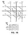
- FIG. 1Aa schematic of a conventional memory array 150 includes a plurality of memory cells 100 arranged in a cross-point configuration with each cell 100 including a conventional MIM diode 106 electrically in series with a memory element 121 , a first terminal 102 , and a second terminal 104 .
- the first terminal 102is electrically coupled with a conductive array line 112 (e.g., a column line) and the second terminal 104 is electrically coupled with a conductive array line 110 (e.g., a row line).
- the conventional MIM diode 106comprises a conventional non-ohmic isolation device.
- the array 150depicts three row conductive array lines denoted as row- 1 , row- 2 , and row- 3 , and three column conductive array lines denoted as col- 1 , col- 2 , and col- 3 .
- the array 150can include fewer or more conductive array lines and memory cells 100 than depicted in FIGS. 1A and 1B .
- voltage potentials for a data operationare applied to the row- 2 and col- 2 conductive array lines (depicted in heavy line) to select a specific memory cell 100 ′ in the array 150 for the data operation.
- the data operationis a write operation to program the selected memory cell 100 ′ (e.g., a programming operation).
- a potential of 0Vis applied to all remaining conductive array lines.
- a table 170depicts the potential difference across the memory cells 100 in the array 150 .
- Memory cells 100 having only one of their two terminals ( 102 or 104 ) electrically coupled with the row- 2 or col- 2 conductive array linesare half-selected memory cells 100 because they have one terminal at 0V and other terminal at +V 1 or ⁇ V 1 . Therefore, the potential difference across those memory cells 100 is +V 1 (e.g., +V 1 ⁇ 0V or 0V ⁇ ( ⁇ V 1 )).
- memory cells 100 having both terminals ( 102 and 104 ) electrically coupled with conductive array lines at the 0V potentialare un-selected memory cells 100 with a potential difference across those memory cells 100 being approximately 0V.
- FIG. 1Bthe array 150 is schematically depicted during an erase operation to the same selected memory cell 100 ′.
- a table 190depicts the potential difference across all the memory cells 100 in the array 150 with un-selected memory cells 100 having a potential difference of approximately 0V and half-selected memory cells 100 having a potential difference of ⁇ V 1 .
- an I-V curve for the memory cells 100 with the conventional MIM diode non-ohmic isolation device 106depicts current flow I (on the y-axis) through a memory cell 100 as a function of the voltage V (on the x-axis) applied across the memory cell 100 .
- the magnitude of the current Iis highest at operating point 212 for the applied voltage of +2V 1 and operating point 214 for the applied voltage ⁇ 2V 1 .
- the magnitude of current Iis expected at those levels of applied voltage for a selected memory cell 100 ′ because that cell is being programmed or erased.
- FIGS. 1A through 2depict applied voltages for program and erase operations, for read operations where the magnitude of the voltage applied across the selected memory cell 100 ′ is typically less than that applied for program and erase operations, there will still be un-selected and half-selected memory cells in the array 150 having a potential difference across their terminals ( 102 , 104 ) that can generate leakage currents that lower the aforementioned S/N ratio during read operations.
- a non-ohmic devicewould allow current to flow only through selected memory cells 100 ′ and would block current flow through half-selected and un-selected memory cells 100 .
- the operating points for half-selected and un-selected memory cells 100would be on the voltage axis V where the current I is 0 A.
- FIG. 1Adepicts a schematic view of a conventional memory array during a programming operation to a memory cell including a conventional MIM diode NOD;
- FIG. 1Bdepicts a schematic view of a conventional memory array during an erase operation to a memory cell including a conventional MIM diode NOD;
- FIG. 2depicts an I-V curve for a memory cell including a conventional MIM diode NOD
- FIG. 3Adepicts a schematic view of a memory array during a programming operation to a memory cell including a single Schottky diode NOD isolation device according to the present invention
- FIG. 3Bdepicts a schematic view of a memory array during a sector erase operation to memory cells including a single Schottky diode NOD isolation devices according to the present invention
- FIG. 3Cdepicts a schematic view of a memory array during a read operation to a memory cell including a single Schottky diode NOD isolation device according to the present invention
- FIG. 4depicts an I-V curve for a memory cell including a single Schottky diode NOD isolation device according to the present invention
- FIG. 5depicts a cross-sectional view of a single Schottky diode NOD isolation device integrated with a memory element in a memory cell according to the present invention
- FIG. 5Adepicts a cross-sectional view of one example of a single Schottky diode NOD isolation device integrated with a memory element in a memory cell according to the present invention
- FIGS. 6A-6Ddepict a cross-sectional views of alternate embodiments of an oxide semiconductor based single Schottky diode NOD isolation device integrated with a memory element in a memory cell according to the present invention
- FIG. 7Adepicts an example of memory cells positioned in a two-terminal cross-point array according to various embodiments of the invention.
- FIG. 7Bdepicts a single layer or multiple vertically stacked layers of memory arrays formed BEOL on top of a base layer including circuitry formed FEOL;
- FIG. 7Cdepicts one example of a vertically stacked memory including multiple array layers that share conductive array lines and formed BEOL on top of a previously formed FEOL base layer;
- FIG. 8Adepicts a cross-sectional view of an integrated circuit die including a single layer of memory fabricated over a substrate including active circuitry fabricated in a logic layer;
- FIG. 8Bdepicts a cross-sectional view of an integrated circuit die including vertically stacked layers of memory fabricated over a substrate including active circuitry fabricated in a logic layer;
- FIG. 8Cdepicts an integrated circuit die including vertically stacked layers of memory with shared conductive array lines fabricated over a substrate including active circuitry fabricated in a logic layer;
- FIG. 9depicts a memory system including a non-volatile two-terminal cross-point array
- FIG. 10depicts an exemplary electrical system that includes at least one non-volatile two-terminal cross-point array
- FIG. 11depicts top plan views of a wafer processed FEOL to form a plurality of base layer die including active circuitry and the same wafer subsequently processed BEOL to form one or more layers of memory directly on top of the base layer die where the finished die can subsequently be singulated, tested, and packed into integrated circuits.
- the memory elementscan be a component of a memory cell that includes electrically in series with the memory element, other structures including but not limited to a non-ohmic device (NOD) and electrodes. New non-volatile memory structures are possible with the capability of this third dimensional memory array.
- NODnon-ohmic device
- the technologyallows for the emulation of other memory technologies by duplicating the interface signals and protocols, while accessing the third dimensional memory array.
- the third dimensional memory arraymay emulate other types of memory (e.g., DRAM, SRAM, FLASH, and ROM), providing memory combinations (e.g., DRAM, FLASH, and SRAM) within a single component.
- a two-terminal memory cellcan be configured to change conductivity when exposed to an appropriate voltage drop across the two-terminals.
- the memory cellcan include an electrolytic tunnel barrier and a mixed valence conductive oxide (e.g., a memory element) in some embodiments, as well as multiple mixed valence conductive oxide structures in other embodiments.
- a voltage drop across the electrolytic tunnel barriercan cause an electrical field within the mixed valence conductive oxide that is strong enough to move oxygen ions out of the mixed valence conductive oxide, according to some embodiments.
- an electrolytic tunnel barrier and one or more mixed valence conductive oxide structuresdo not need to operate in a silicon substrate, and, therefore, can be fabricated (e.g., back-end-of-the-line BEOL) above circuitry being used for other purposes (e.g., circuitry fabricated front-end-of-the-line FEOL).
- the circuitry portion of an ICcan be fabricated FEOL on a substrate (e.g., a silicon Si wafer) that is partitioned into die with each die forming the base structure for the IC. After the FEOL processing is completed the substrate is processed BEOL to fabricate the one or more layers of memory directly on top of each FEOL die.
- An inter-level interconnect structure formed FEOLserves as the structural and electrical foundation for the subsequent formation of the one or more layers of memory that will be deposited (e.g., formed) on top of the FEOL die.
- the inter-level interconnect structureincludes vias, plugs, damascene structures or the like, that allow the FEOL circuitry to be electrically coupled with the BEOL memory layer(s).
- the finished diecan be singulated from the substrate (e.g., removed by sawing or cutting) to form individual die that can be inserted into a suitable package and electrically coupled with bonding pads or other structures in the package to form an integrated circuit (IC).
- each dieis an integral unit that includes at a bottommost layer the FEOL circuitry and upper layers comprised of one or more layers of third dimensional memory that are positioned above the FEOL circuitry layer.
- the BEOL third dimensional memory layer(s)are not on the same plane as the FEOL circuitry and therefore do not take up area on the FEOL die. Accordingly, data storage can be increased without increasing the area of the FEOL die by fabricating additional BEOL memory layers on top of the FEOL die (e.g., along the +Z axis of FIGS. 7B-8C ).
- a two-terminal memory cellcan be arranged in a cross-point configuration such that one terminal is electrically coupled with an X-direction line (or an “X-line”) and the other terminal is electrically coupled with a Y-direction line (or a “Y-line”).
- a third dimensional memorycan include multiple memory cells vertically stacked upon one another, sometimes sharing X-direction and Y-direction lines in a layer of memory, and sometimes having electrically isolated X and Y direction lines (e.g., using a dielectric material such as SiO 2 ).
- VW 1When a first write voltage, VW 1 , is applied across the memory cell (e.g., by applying 1 ⁇ 2 VW 1 to the X-direction line and 1 ⁇ 2-VW 1 to the Y-direction line), the memory cell can switch to a low resistive state.
- VW 2When a second write voltage, VW 2 , is applied across the memory cell (e.g., by applying 1 ⁇ 2 VW 2 to the X-direction line and 1 ⁇ 2-VW 2 to the Y-direction line), the memory cell can switch to a high resistive state.
- Memory cells using electrolytic tunnel barriers and mixed valence conductive oxidescan have VW 1 opposite in polarity from VW 2 .
- FIG. 3Aa schematic of a memory array 350 is depicted.
- the array 350is a 3 ⁇ 3 array with three row conductors denoted as row- 1 , row- 2 , and row- 3 and three columns conductors denoted as col- 1 , col- 2 , and col- 3 ; however, the array 350 can be any size and is not limited to the 3 ⁇ 3 array depicted in FIG. 3A .
- the array 350can include a plurality of two-terminal memory cells 300 positioned in a cross-point array configuration with each memory cell 300 including a first terminal 304 electrically coupled with one of the row conductors and a second terminal 306 electrically coupled with one of the column conductors.
- Each memory cell 300further includes a two-terminal memory element 302 and a single Schottky diode 321 non-ohmic isolation device (NOD) that are electrically in series with each other and electrically in series with the terminals 304 and 306 .
- NODnon-ohmic isolation device
- Data operations (e.g., read and write operations) on the memory cells 300require appropriate voltage potentials be applied to selected conductive array lines.
- a write operatione.g., a programming operation
- the selected memory cellis denoted as 300 ′.
- the remaining row conductorshave voltage potential of ⁇ V 1 applied to them and the remaining column conductors have a voltage potential of +V 1 applied to them.
- a programming table 370depicts the voltage across the selected memory cell 300 ′ and across un-selected memory cells 300 .
- the selected memory cell 300 ′has a potential difference of +2V 1 across its terminals ( 304 , 306 ) and un-selected memory cells 300 have a 0V or a ⁇ 2V 1 potential difference across their terminals ( 304 , 306 ).
- the applied voltagescan be shifted up or down relative to what is depicted in FIG. 3A and are not limited to the +V 1 and ⁇ V 1 shown.
- the terminology un-selected memory cell 300means any memory cell 300 that is not the selected memory cell 300 ′ even though some of the memory cells 300 can be designated as half-selected memory cells 300 .
- cells 300 denoted as HSare half-selected memory cells
- cells 300 denoted as USun-selected memory cells.
- the asymmetrical characteristics of the single Schottky diode 321 and 621allow tolerable levels of unselected cell 300 leakage in the array 350 (e.g., approximately a 4000:1 current ratio between the selected device 300 ′ and an unselected devices 300 with the same voltage at reverse polarity).
- the reverse leakage characteristics of the single Schottky diode 321are expected to be better than the half-selected leakage characteristics of the conventional MIM diode 106 described above in reference to FIGS. 1A-2 .
- the Schottky diode ( 321 , 621 )is not subject to dielectric breakdown failure mechanisms such as time-dependent dielectric breakdown or stress-induced leakage current.
- the current and total fluence (C/cm 2 ) that may be passed through the single Schottky diode ( 321 , 621 ) before failureis much higher than that of the conventional MIM diode 106 .
- the single Schottky diode ( 321 , 621 )has a well-controlled reverse breakdown voltage; sector erase is possible by biasing the diodes ( 321 , 621 ) on multiple cells 300 into reverse breakdown.
- FIG. 3Ba schematic depicts a sector erase operation (also referred to as a block erase operation) to the array 350 .
- all the row conductors 310have an applied voltage potential of ⁇ V 2 and all the column conductors 312 have an applied voltage potential of +V 2 . Consequently, all the memory cells are selected for the erase operation and are denoted as selected memory cells 300 ′.
- Variations on the erase operation of FIG. 3Bcan include erasing the memory cells 300 ′ in a selected column of the array 350 or in a selected row of the array 350 .
- column conductors col- 1 and col- 2can have a voltage potential of approximately 0V applied to them
- col- 3can have a voltage potential of +V 2 applied to it
- row conductors row- 1 , row- 2 , and row- 3can have a voltage potential of ⁇ V 2 applied to them.
- all of the memory cells 300 in col- 1 and col- 2are half-selected during the erase operation with a potential difference of ⁇ V 2 (e.g., ⁇ V 2 ⁇ 0V) across their terminals and in col- 3 all of the memory cells 300 ′ are selected for the erase operation and have a potential difference of ⁇ 2V 2 (e.g., ⁇ V 2 ⁇ (+V 2 )) across their terminals.
- ⁇ V 2e.g., ⁇ V 2 ⁇ 0V
- row conductors row- 1 and row- 3can have a voltage potential of approximately 0V applied to them
- row- 2can have a voltage potential of ⁇ V 2 applied to it
- column conductors col- 1 , col- 2 , and col- 3can have a voltage potential of +V 2 applied to them.
- all of the memory cells 300 in row- 1 and row- 3are half-selected during the erase operation with a potential difference of +V 2 (e.g., 0V ⁇ ( ⁇ V 2 )) across their terminals and in row- 2 all of the memory cells 300 ′ are selected for the erase operation and have a potential difference of ⁇ 2V 2 (e.g., ⁇ V 2 ⁇ (+V 2 )) across their terminals.
- +V 2e.g., 0V ⁇ ( ⁇ V 2 )
- ⁇ 2V 2e.g., ⁇ V 2 ⁇ (+V 2 )
- FIG. 3Ca schematic depicts a read operation performed on a single selected memory cell 300 ′ in the array 350 .
- all the unselected row conductors 310have an applied voltage potential of ⁇ V 3 and all un-selected column conductors 312 have an applied voltage potential of +V 3 , with the selected memory cell 300 ′ having voltage potentials of +V 3 and ⁇ V 3 applied to its row 310 and column 312 conductors, respectively.
- a read table 390depicts the potential difference across the terminals of the selected 300 ′ and un-selected memory cells 300 .
- Un-selected memory cells 300have a potential difference of ⁇ 2V 3 or 0V; whereas, the selected memory cell 300 ′ has a potential difference of +2V 3 .
- the magnitude of read voltagesare typically less than the magnitude of voltages for program or erase operations because a lower magnitude of read voltage prevents data stored in the selected memory cell(s) 300 ′ from being overwritten or corrupted during read operations.
- the erased conductivity profilecomprises a low resistance state (e.g., erased conductivity is high) then the magnitude of the read current I R will be higher when the memory cell 300 ′ is in the erased state. Therefore, given the previous examples, I R-Erased >I R-Programmed .
- the actual conventions for the resistance or conductivity values for programmed and erased stateswill be application dependent and the foregoing is just one example of how the programmed and erased states can be defined.
- the read current I R signalalong with one or more other signals (e.g., leakage currents and/or reference signals) can be electrically coupled with sense circuitry (e.g., FEOL active circuitry) that compares those signals in the current or voltage domains to generate a signal that is indicative of the valued of data stored in the selected memory cell(s) 300 ′.
- sense circuitrye.g., FEOL active circuitry
- an I-V curve 400depicts a non-linear relationship between current I on a y-axis and voltage V on an x-axis for a memory cell 300 that includes the Schottky diode NOD ( 321 , 621 ).
- Operating points 403 and 405 for selected memory cells 300 ′depict current flow I through the selected memory cell(s) 300 ′ at a potential difference along the x-axis of +2V 1 at an operating point 403 and ⁇ 2V 2 at an operating point 405 .
- an operating point 404 for un-selected memory cells 300depicts very low current flow I for a potential difference along the x-axis of ⁇ 2V 1 such that a reverse current at ⁇ 2V 1 is orders of magnitude lower than a forward current at 2V 1 . Therefore, from about 0V on the x-axis at a point 406 to a point 408 located between voltages ⁇ 2V 2 and ⁇ 2V 1 , the reverse current for I is substantially lower than the forward current for I from the point 410 to 403 .
- FIG. 3Awhere un-selected memory cells 300 either have a potential difference across their terminals of 0V or ⁇ 2V 1 , current I is very low (e.g., at operating point 404 ) during the program operation to selected memory cell 300 ′.
- FIG. 3Bsince all of the memory cells are selected memory cells 300 ′ during the sector erase operation, all of the selected memory cells 300 ′ have a current I at the operating point 405 at ⁇ 2V 2 .
- operating points 410 and 412can depict a range of read currents I R that flow when the read voltage +2V 3 is applied across the terminals ( 304 , 306 ) of the selected memory cell 300 ′.
- the Schottky diode ( 321 , 621 )may be readily integrated into a back-end process for fabricating BEOL memory layers.
- amorphous siliconmay be subjected to a rapid thermal annealing step (e.g., at a temperature of about 700° C.) that converts the amorphous silicon to a single layer of polycrystalline silicon (also called polysilicon or poly-Si).
- a lightly doped n-type polysilicon line atop a metal plug on the memory devicewill produce a Schottky diode.
- Resistivity of the polysilicon linemay be reduced by siliciding (e.g., reacting with Ni or Co) the top surface of the polysilicon to form a silicide layer (e.g., nickel silicide or cobalt silicide).
- silicidinge.g., reacting with Ni or Co
- the Schottky diode ( 321 , 621 )should be easier to integrate than a p-n junction diode, in addition to having a better controlled reverse breakdown voltage.
- a silicon wafer including active circuitrye.g., CMOS devices fabricated thereon during a front-end-of-the-line process (FEOL) can include with the active circuitry, the circuits (drivers, decoders, sense amps, buffers, registers, etc.) that interface with the BEOL array 350 for data operations (e.g., read, program, and erase) to the memory cells 300 .
- active circuitrye.g., CMOS devices
- FEOLfront-end-of-the-line process
- the BEOL array 350can be fabricated directly on top of the silicon wafer and its active circuitry as part of a back-end-of-the-line process (BEOL).
- BEOLback-end-of-the-line process
- one layer of cross-point memory array 350 or multiple layers of vertically stacked cross-point memory arrays 350can be formed.
- a single layer of polycrystalline siliconhas advantages over using one or more layers of amorphous silicon (also referred to as ⁇ -Si or a-Si) to form a Schottky diode.
- polycrystalline siliconhas a mobility of charge carriers (e.g., in cm 2 /V ⁇ s) that can be orders of magnitude higher than that of amorphous silicon. For example, if a typical mobility of amorphous silicon is approximately less than 1 cm 2 /V ⁇ s, then a typical mobility of polycrystalline silicon can be approximately 10 cm 2 /V ⁇ s or more.
- the higher mobility of charge carriers for polycrystalline siliconis desirable for supporting higher current flows through the memory cell 300 during data operations to the memory cells (see FIG.
- a higher read current I Rcan reduce read errors in sense amp circuitry by increasing the signal to noise ratio (S/N) such that the signal representing the read current I R in the memory cell 300 ′ being read is easy to distinguish over noise signals that may be present during read operations.
- S/Nsignal to noise ratio
- the ability of polycrystalline silicon to support higher currentscan be desirable during program and erase operations because the magnitude the voltage applied across the memory cell 300 during write operations is typically larger than the magnitude of the read voltage, resulting in larger magnitude currents I during write operations.
- amorphous siliconsuch as intrinsic ⁇ -Si and/or doped ⁇ -Si (e.g., doped n+) can be formed at lower processing temperatures than polycrystalline silicon, the higher processing temperatures required to form the singly layer of polycrystalline silicon are worthwhile given the larger currents that can be supported by the polycrystalline silicon.
- each memory cell 300can include two terminals ( 304 , 306 ) electrically coupled with their respective pair of conductive array lines ( 310 , 312 ) and the memory cell 300 can be positioned at a cross-point of its respective conductive array lines ( 310 , 312 ).
- Each memory cell 300can include electrically in series with its terminals and electrically in series with each other, the memory element 302 and the Schottky diodes ( 321 , 621 ), such that the Schottky diode ( 321 , 621 ) is integral with the memory cell 300 .
- FIG. 5a cross-sectional view of a structure for a memory cell 300 that includes a memory element 302 and the single Schottky diode NOD 321 is depicted.
- a layer of metal 529can be formed on top of the memory element 302 followed by a deposition of a single layer of lightly doped polycrystalline silicon (polysilicon) 523 on top of the layer of metal 529 to form the single Schottky diode NOD 321 , and a silicide layer 527 formed on top of the polysilicon layer 523 .
- polysiliconlightly doped polycrystalline silicon
- the single layer of polysilicon 523may initially be amorphous silicon that is annealed, heated, or otherwise transformed from an amorphous silicon structure to a polycrystalline silicon structure. It may be necessary to form an ohmic contact between the polysilicon layer 523 and the silicide layer 527 . Accordingly, a portion 525 (e.g., the portion above dashed line 524 ) of the single layer of polysilicon 523 can be doped with a doping type that is opposite to the type of doping for the lightly doped layer 523 . For example, the polysilicon layer 523 can be lightly doped n ⁇ and the portion 525 can be doped n+. Subsequently, a silicide layer 527 can be deposited on the portion 525 to form the ohmic contact between layers 523 and 527 .
- FIG. 5Adepicts a cross-sectional view of one example for a structure for the Schottky diode NOD 321 formed by contact between a layer of metal 529 and a single layer of n ⁇ polysilicon 523 .
- the single layer of n ⁇ polysilicon 523includes a second portion comprised of n+ polysilicon 525 which is in contact with a layer of a silicide material 527 .
- the layer of metal 529is positioned on top and in contact with the memory element 302 .
- the arrangement depictedis just one example and the layers ( 523 , 529 ) need not be in direct contact with the memory element 302 and the memory element 302 can be positioned above the layer of metal 529 and the other layers of material for the Schottky diode NOD 321 .
- the memory element 302 and the NOD 321are electrically in series with each other, their relative positions in the memory cell 300 can be determined by processing requirements and/or design requirements. Accordingly, the NOD 321 and memory element 302 need not be in contact with each other.
- 5 and 5Aneed not be in direct physical contact with the memory element 302 and some other electrically conductive structure in the memory cell 300 (e.g., an electrically conductive glue or adhesion layer) can be positioned between the NOD 321 and the memory element 302 .
- Current flow through the memory cell 300can be accomplished by placing a potential difference of ⁇ 0.5V across the terminals ( 304 , 306 ) of the memory cell 300 (e.g., ⁇ 0.5V on terminal 304 and 0V on terminal 306 ) or a potential difference of +4V across the terminals (e.g., +4V on terminal 304 and 0V on terminal 306 ).
- Suitable materials for the layer of silicide 527include but are not limited to a nickel Ni silicide and a cobalt Co silicide, for example.
- Suitable materials for the layer of metal 529include but are not limited to tungsten (W), aluminum (Al), and platinum (Pt), for example.
- the metal layer 529can be a structure such as a metal plug processed using a planarization technique such as CMP to form a substantially planar upper surface upon which to deposit the single layer 523 .
- a single layer of amorphous silicon Sican be deposited on the metal layer 529 and surface doped (e.g., n ⁇ ) using a low-energy implant or a POCl 3 reaction.
- the single layer 523can be subjected to rapid thermal annealing to convert the amorphous Si into polycrystalline Si and to activate the dopant. Annealing temperatures will be application dependent; however, the annealing temperature can be about 700° C. or about 500° C. or lower if metal-assisted crystallization is used. Subsequently, the single layer 523 can be patterned and etched. Additional thin film layers required by the memory cell 300 can be deposited on the layer 523 or 527 , such as a silicon nitride SiN 3 spacer layer, for example.
- FIGS. 6A through 6Ddepict alternate examples for the single Schottky diode NOD 621 based on a single layer of an oxide semiconductor material 611 .
- the NOD 621 and memory element 302are depicted in contact with each other, as was described above, the NOD 621 and memory element 302 need not be in contact with each other.
- the Schottky diode NOD 621is similar to the NOD 321 of FIGS. 5 and 5A , but the NOD 621 utilizes an oxide semiconductor in place of the lightly doped polysilicon 523 and can use different materials for the metal electrodes.
- the single layer of oxide semiconductor material 611is sandwiched between and is in contact with non-ohmic metal 613 and ohmic-metal 612 .
- the non-ohmic metal 613is shared with the memory element 302 .
- the non-ohmic metal 613is in contact with a metal layer 615 such that a metal/oxide semiconductor/metal structure is positioned on top of the memory element 302 .
- the single layer of oxide semiconductor material 611is in contact with and is sandwiched between and ohmic metal ( 623 , 633 ) and non-ohmic metal ( 622 , 632 ).
- FIG. 6Athe non-ohmic metal 613 is shared with the memory element 302 .
- the non-ohmic metal 613is in contact with a metal layer 615 such that a metal/oxide semiconductor/metal structure is positioned on top of the memory element 302 .
- the single layer of oxide semiconductor material 611is in contact with and is sandwiched between and
- the ohmic metal 623is in contact with a metal layer 615 such that a metal/oxide semiconductor/metal structure is positioned on top of the memory element 302 .
- the ohmic metal 633is shared with the memory element 302 .
- the memory element 302may be positioned at the bottom of the stack for memory cell 300 as depicted or may be positioned at the top of the stack for the memory cell 300 (not shown).
- Suitable materials for the oxide semiconductor 611include but are not limited to perovskites and binary oxides.
- the perovskitecan be a doped SrTiO 3 (e.g., doped with niobium Nb or lanthanum La), for example.
- the binary oxidecan be nickel oxide NiO x , zinc oxide ZnO x , or tin oxide SnO x , for example.
- Suitable non-ohmic metalsinclude but are not limited to platinum Pt, palladium Pd, and iridium Ir.
- Suitable ohmic metalsinclude but are not limited to magnesium Mg, indium In, aluminum Al, and tantalum Ta.
- Suitable materials for the metal 615include but are not limited to platinum Pt, iridium Ir, and iridium oxide IrO x .
- the ohmic metalmay not be necessary if the oxide semiconductor 611 includes a graded doping profile with a very high doping profile at the ohmic interface, that is, the doping concentration is highest at the ohmic interface.
- the NOD 621can be fabricated using processing steps including but not limited to metal deposition, CMP to produce metal plugs, oxide semiconductor 611 deposition, graded-doping of the oxide semiconductor 611 during deposition or post deposition using implantation, patterning and etching the oxide semiconductor 611 , annealing for contact improvement, and deposition of additional layers of material, such as glue layers, for example.
- the memory element 302can be comprised of discrete layers of material (e.g., etched layers in the stack for memory cell 300 ) or can be continuous and un-etched layers of material that include one or more layers of a conductive metal oxide (CMO) that are in contact with each other and are continuous and un-etched layers and a continuous and un-etched electronically insulating layer (e.g., yttria-stabilized zirconia—YSZ) in contact with an uppermost of the CMO layers.
- CMOconductive metal oxide
- YSZyttria-stabilized zirconia
- Portions of the one or more layers of CMO that are positioned in the stack for memory cell 300can be electrically conductive and portions outside of the stack can be made electrically nonconductive insulating metal oxides (IMO's) by treating those portions to transform them from conductive to insulating (e.g., by ion implantation).
- IMO'selectrically nonconductive insulating metal oxides
- portions of the memory stacke.g., an electrode, a hard mask layer, or the NOD 321 or 621
- portions of the memory stackcan be used as an implantation mask operative to shield the portion of the CMO layer that is to remain electrically conductive from the ions during implantation such that the portions of the CMO layer positioned outside the memory stack are bombarded by the ions and are transformed into IMO's.
- FIG. 7Adepicts an example of arrayed memory cells according to various embodiments of the invention.
- a memory cell 300includes a memory element 302 and NOD 321 positioned above or below (not shown) the memory element 302 .
- the memory element 302can include the above mentioned CMO layer(s) and electronically insulating layer denoted as 710 and 712 respectively.
- the layers 710 and 712can be discrete layers as depicted or they can be continuous and un-etched layers (not shown) as described above.
- Memory cell 300further includes terminals 771 and 773 . Terminals 771 and 773 can be electrically coupled with or can be formed as electrodes 774 and 778 .
- the electrodes ( 774 , 778 )can be made from an electrically conductive material including, but not limited to, platinum (Pt), gold (Au), silver (Ag), iridium (Ir), iridium oxide (IrO x ), ruthenium (Ru), palladium (Pd), aluminum (Al), alloys of those materials, and the like.
- the electrodes ( 774 , 778 )can be in contact with and/or electrically coupled with conductive array lines operative to apply the aforementioned voltages for data operations, such as read voltages and write voltages (e.g., program and erase voltages) across one or more selected memory cells 300 .
- the memory element 302 and NOD 321are electrically in series with each other and electrically in series with the electrodes ( 774 , 778 ).
- Memory cell 300can be formed between conductive array lines, such as array lines 312 and 310 .
- memory cell 300can be formed in an array of other memory cells 300 .
- array lines 312 ′ and 310 ′are depicted in heavy line to illustrate that those array lines have voltages for data operations applied to them such that memory cell 300 ′ is the selected memory cell for the data operation.
- the arraycan be the cross-point array 350 including groups of conductive array lines 310 and 312 .
- array lines 310can be electrically coupled with the electrodes 774 of the memory cells 300 and/or may be in contact with a surface 772 s of the electrodes 774
- array lines 312can be electrically coupled with the electrodes 778 of the memory cells 300 and/or may be in contact with a surface 778 s of the electrodes 778 .
- the active circuitry that applies the voltages for data operationsis positioned below the array 350 on a substrate with the array 350 fabricated directly on top of the substrate and the array 350 in contact with the substrate.
- FIG. 7Bdepicts an integrated circuit including memory cells disposed in a single layer or in multiple layers of memory, according to various embodiments of the invention.
- integrated circuit 780is shown to include either multiple layers 750 of memory (e.g., layers 752 a, 752 b, . . . 752 n ) or a single memory layer 751 (e.g., layer 752 ) formed on a base layer 754 .
- layers 754 and 752 a, 752 b, . . . 752 n or layers 754 and 752are not physically separate layers as depicted in FIG.
- each layer(e.g., layer 752 or layers 752 a, 752 b, . . . 752 n ) of memory can be a cross-point memory array 350 including conductive array lines 310 and 312 arranged in different directions to access re-writable memory cells 300 such as two-terminal memory cells as described above.
- Base layer 754can include a bulk semiconductor substrate (e.g., a silicon wafer) upon which memory access circuits 753 for performing data operations on the memory cells 300 in memory 750 or 751 are fabricated.
- Base layer 754may include other circuitry that may or may not be related to data operations on memory.
- Base layer 754 and circuitry 753can be formed in a front-end-of-the-line (FEOL) fabrication process and multiple memory layers 750 or single memory layer 751 can be formed in a back-end-of-the-line (BEOL) fabrication process tailored to fabricating layer(s) of memory arrays on top of the base layer 754 .
- FEOLfront-end-of-the-line
- BEOLback-end-of-the-line
- the base layer 754can include an inter-level interconnect structure configured to include nodes (e.g., openings in a dielectric material or electrically conductive structures such as vias, plugs, thrus, damascene structures, etc.) for facilitating electrical coupling between the circuitry 753 and the conductive array lines ( 310 , 312 ) of the array(s) so that signals (e.g., read and write voltages) for data operations (e.g., read and write operations) are electrically communicated between the array(s) and the circuitry 753 .
- the inter-level interconnect structurecan be one of the last microelectronic structures fabricated during the FEOL processing.
- a vertically stacked array 790includes a plurality of memory layers A,B,C, and D with each memory layer including memory cells 300 a, 300 b, 300 c, and 300 d. Although only four layers are depicted, the array 790 can include fewer layers or can include additional layers up to an nth layer.
- the array 790includes three levels of x-direction conductive array lines 710 a, 710 b, and 710 c, and two levels of y-direction conductive array lines 712 a, and 712 b.
- the 7Cshare conductive array lines with other memory cells that are positioned above, below, or both above and below that memory cell.
- the conductive array lines, the memory cells, dielectric materials that electrically isolate structures in the array 790 (not shown), and other structures in the array 790are formed BEOL above the base layer 754 (not shown) as indicated by +Z on the Z-axis above the dashed line at origin 0 ; whereas, the active circuitry for performing data operations on the array 790 and the interconnect structure for electrically coupling the active circuitry with the array 790 (e.g., the conductive array lines) are previously formed FEOL as indicated by ⁇ Z on the Z-axis below the dashed line at origin 0 .
- the BEOL structure for array 790is formed on top of the FEOL structure for base layer 754 with the order of fabrication going in a direction from ⁇ Z (i.e., FEOL) to +Z (i.e., BEOL) along the Z-axis.
- integrated circuit 780includes the base layer 754 and active circuitry 753 fabricated on the base layer 754 (e.g., a silicon Si wafer).
- the integrated circuit 780is comprised of a single unitary die 800 having a first portion (i.e., the base layer 754 ) fabricated first using FEOL processing and a second portion (i.e., the single memory layer 752 ) fabricated second and formed directly on top of the base layer 754 using BEOL processing, such that the second portion is integrally formed with the first portion and completes the formation of the die 800 .
- the base layer 754can be a silicon (Si) wafer and the active circuitry 753 can be microelectronic devices formed on the base layer 754 using a CMOS fabrication process.
- the memory cells 300 and their respective conductive array lines ( 310 , 312 )can be fabricated on top of the active circuitry 754 in the base layer 754 .
- an inter-level interconnect structure(not shown) can electrically couple the conductive array lines ( 310 , 312 ) with the active circuitry 753 which may include several metal layers.
- viascan be used to electrically couple the conductive array lines ( 310 , 312 ) with the active circuitry 753 .
- the active circuitry 753may include but is not limited to address decoders, sense amps, memory controllers, data buffers, direct memory access (DMA) circuits, voltage sources for generating the read and write voltages, just to name a few.
- Active circuits 810 - 818can be configured to apply the select voltage potentials (e.g., read and write voltage potentials) to selected conductive array lines ( 310 ′, 312 ′).
- the active circuitry 753may be electrically coupled with the conductive array lines ( 310 ′, 312 ′) to sense a read current I R that flows through selected memory cells 300 ′ during a read operation and the read current I R can be sensed and processed by the active circuitry 753 to determine the conductivity profiles (e.g., the resistive state) of the selected memory cells 300 ′.
- Examples of conductivity profilesinclude but are not limited to a programmed conductivity profile written to a memory cell 300 ′ during a programming data operation and an erased conductivity profile written to a memory cell 300 ′ during an erase data operation.
- Memory cells 300can store data as a plurality of conductivity profiles that can include the programmed or erased conductivity profiles only (e.g., only 1-Bit of data stored per memory cell 300 ) or more than two conductivity profiles for storing multiple bits of data per memory cell 300 (e.g., two or more bits of data per memory cell 300 ).
- the direction of current flow for the read current I Rwill depend on a magnitude and polarity of a read voltage applied across terminals 304 and 306 . In some applications, it may be desirable to prevent un-selected array lines ( 310 , 312 ) from floating.
- the active circuits 753can be configured to apply an un-select voltage potential (e.g., approximately a ground potential) to the un-selected array lines ( 310 , 312 ).
- a dielectric material 811e.g., SiO 2 ) may be used where necessary to provide electrical insulation between elements of the integrated circuit 780 .
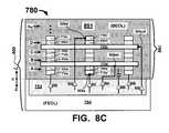
- an integrated circuit 780includes a plurality of non-volatile memory arrays that are vertically stacked above one another (e.g., along a +Z axis) and are positioned above the base layer 754 that includes the active circuitry 753 .
- the integrated circuit 780includes vertically stacked memory layers A and B and may include additional memory layers up to an nth memory layer.
- the memory layers A, B, . . . through the nth layercan be electrically coupled with the active circuitry 753 in the base layer 754 by an inter-level interconnect structure as was described above.
- Layer Aincludes memory cells 300 a and first and second conductive array lines ( 310 a, 312 a )
- Layer Bincludes memory cells 300 b and first and second conductive array lines ( 310 b, 312 b )
- the nth layerincludes memory cells 300 n and first and second conductive array lines ( 310 n, 312 n ).
- Dielectric materials 825 a, 825 b, and 825 nmay be used where necessary to provide electrical insulation between elements of the integrated circuit 820 .
- Active circuits 840 - 857can be configured to apply the select voltage potentials (e.g., read and write voltage potentials) to selected conductive array lines (e.g., 310 a, b, n, and 312 a, b, n ).
- Driver circuits 850 and 857are activated to select conductive array lines 310 ′ and 312 ′ to select memory cell 300 b′ for a data operation.
- the active circuits 753can be used to sense the read current I R (not shown) from selected memory cells 300 b′ during a read operation and can be configured to apply the un-select voltage potential to the un-selected array lines.
- the integrated circuit 780comprises the die 800 that is a unitary whole comprised of a FEOL circuitry portion fabricated on base layer 754 and a BEOL memory portion having multiple memory layers that is in contact with the FEOL portion and is fabricated directly on top of the FEOL portion.
- an integrated circuit 780includes base layer 754 , active circuitry 753 , and vertically staked memory layers A, B, C, and D that are fabricated above the base layer 754 .
- Active circuits 840 - 857are configured to perform data operations on the vertically staked memory layers A, B, C, and D.
- Driver circuits 844 and 857are activated to select memory cell 300 a ′ for a data operation and driver circuits 842 and 848 are activated to select memory cell 600 d′ for a data operation.
- a dielectric layer 851is operative to electrically isolate the various components of integrated circuit 780 .
- the integrated circuit 780comprises the die 800 that is a unitary whole comprised of a FEOL circuitry portion fabricated on base layer 754 and a BEOL memory portion having multiple memory layers that is in contact with the FEOL portion and is fabricated directly on top of the FEOL portion.
- an exemplary memory system 900includes the aforementioned non-volatile two-terminal cross-point memory array 350 (array 350 hereinafter) and the plurality of first conductive and second conductive traces denoted as 310 and 312 , respectively.
- the memory system 900also includes an address unit 903 and a sense unit 905 .
- the address unit 903receives an address ADDR, decodes the address, and based on the address, selects at least one of the plurality of first conductive traces (denoted as 310 ′) and one of the plurality of second conductive traces (denoted as 312 ′).
- the address unit 903applies select voltage potentials (e.g., read or write voltages) to the selected first and second conductive traces 310 ′ and 312 ′.
- the address unit 903also applies a non-select voltage potential to unselected traces 310 and 312 .
- the sense unit 905senses one or more currents flowing through one or more of the conductive traces. During a read operation to the array 350 , current sensed by the sense unit 905 is indicative of stored data in a memory cell 300 ′ positioned at an intersection of the selected first and second conductive traces 310 ′ and 312 ′.
- a bus 921 coupled with an address bus 923can be used to communicate the address ADDR to the address unit 903 .
- the sense unit 905processes the one or more currents and at least one additional signal to generate a data signal DOUT that is indicative of the stored data in the memory cell.
- the sense unit 905may sense current flowing through a plurality of memory cells and processes those currents along with additional signals to generate a data signal DOUT for each of the plurality of memory cells.
- a bus 927communicates the data signal DOUT to a data bus 929 .
- the address unit 903receives write data DIN to be written to a memory cell specified by the address ADDR.
- a bus 925communicates the write data DIN from the data bus 929 to the address unit 903 .
- the address unit 903determines a magnitude and polarity of the select voltage potentials to be applied to the selected first and second conductive traces 310 ′ and 312 ′ based on the value of the write data DIN. For example, one magnitude and polarity can be used to write a logic “0” and a second magnitude and polarity can be used to write a logic “1”.
- the memory system 900can include dedicated circuitry that is separate from the address unit 903 to generate the select potentials and to determine the magnitude and polarity of the select potentials.
- the memory system 900 and its componentscan be electrically coupled with and controlled by an external system or device (e.g., a microprocessor or a memory controller).
- the memory system 900can include at least one control unit 907 operative to coordinate and control operation of the address and sense units 903 and 905 and any other circuitry necessary for data operations (e.g., read and write operations) to the array 350 .
- the array 350can comprise a single layer of memory (e.g., 752 ) or multiple layers of vertically stacked memory ( 752 a, 752 b, . . . 752 n ) as depicted in FIGS.
- One or more signal lines 909 and 911can electrically couple the control unit 907 with the address and sense units 903 and 905 .
- the control unit 907can be electrically coupled with an external system (e.g., a microprocessor or a memory controller) through one or more signal lines 913 .
- one or more of the arrays 350can be positioned over a substrate 754 that includes active circuitry 753 and the active circuitry 753 can be electrically coupled with the array(s) 350 using an interconnect structure that couples signals from the active circuitry 753 with the conductive array lines 310 and 312 .
- the busses, signal lines, control signals, the address, sense, and control units 903 , 905 , and 907can comprise the active circuitry 753 and its related interconnect, and can be fabricated on the substrate 754 (e.g., a silicon wafer) using a microelectronics fabrication technology, such as CMOS, for example.
- an electrical system 1000includes a CPU 1001 that is electrically coupled 1004 with a bus 1002 , an I/O unit 1007 that is electrically coupled 1010 with the bus 1002 , and a storage unit 1005 that is electrically coupled 1008 with the bus 1002 .
- the I/O unit 1007is electrically coupled 1012 to external sources (not shown) of input data and output data.
- the CPU 1001can be any type of processing unit including but not limited to a microprocessor ( ⁇ P), a micro-controller ( ⁇ C), and a digital signal processor (DSP), for example.
- the storage unit 1005stores at least a portion of the data in the aforementioned non-volatile two-terminal cross-point array as depicted in FIGS. 5 through 8C .
- Each memory arrayincludes a plurality of the two-terminal memory cells 300 .
- the configuration of the storage unit 1005will be application specific.
- Example configurationsinclude but are not limited to one or more single layer non-volatile two-terminal cross-point arrays (e.g., 752 ) and one or more vertically stacked non-volatile two-terminal cross-point arrays (e.g., 752 a - 752 n ).
- the CPU 1001may include a memory controller (not shown) for controlling data operations to the storage unit 1005 .
- the electrical system 1000may include the CPU 1001 and the I/O unit 1007 coupled with the bus 1002 , and a memory unit 1003 that is directly coupled 1006 with the CPU 1001 .
- the memory unit 1003is configured to serve some or all of the memory needs of the CPU 1001 .
- the CPU 1001and optionally the I/O unit 1007 , executes data operations (e.g., reading and writing data) to the non-volatile memory unit 1003 .
- the memory unit 1003stores at least a portion of the data in the aforementioned non-volatile two-terminal cross-point array as depicted in FIGS. 7A through 8C .
- Each memory arraycan include a plurality of the two-terminal memory cells 300 with each memory cell 300 including the two-terminal memory element 302 and the Schottky diode NOD ( 321 , 621 ).
- the configuration of the memory unit 1003will be application specific. Example configurations include but are not limited to one or more single layer non-volatile two-terminal cross-point arrays (e.g., 752 ) and one or more vertically stacked non-volatile two-terminal cross-point arrays (e.g., 752 a - 752 n ).
- data stored in the memory unit 1003is retained in the absence of electrical power.
- Data and program instructions for use by the CPU 1001may be stored in the memory unit 1003 .
- the CPU 1001may include a memory controller (not shown) for controlling data operations to the non-volatile memory unit 1003 .
- the memory controllermay be configured for direct memory access (DMA).
- FIG. 11where a top plan view depicts a single wafer (denoted as 1170 and 1170 ′) at two different stages of fabrication: FEOL processing on the wafer denoted as 1170 during the FEOL stage of processing where active circuitry 753 is formed; followed by BEOL processing on the same wafer denoted as 1170 ′ during the BEOL stage of processing where one or more layers of non-volatile memory are formed.
- Wafer 1170includes a plurality of the base layer die 754 (see FIGS. 7B-8C ) formed individually on wafer 1170 as part of the FEOL process. As part of the FEOL processing, the base layer die 754 may be tested 1172 to determine their electrical characteristics, functionality, performance grading, etc.
- the wafer 1170is optionally transported 1104 for subsequent BEOL processing (e.g., adding one or more layers of memory such as single layer 752 or multiple layers 752 a, 752 b, . . . 752 n ) directly on top of each base layer die 754 .
- a base layer die 754is depicted in cross-sectional view along a dashed line FF-FF where the substrate the die 754 is fabricated on (e.g., a silicon Si wafer) and its associated active circuitry are positioned along the axis.
- the one or more layers of memoryare grown directly on top of an upper surface 754 s of each base layer die 754 as part of the subsequent BEOL processing.
- the wafer 1170is denoted as wafer 1170 ′, which is the same wafer subjected to additional processing to fabricate the memory layer(s) directly on top of the base layer die 754 .
- Base layer die 754 that failed testingmay be identified either visually (e.g., by marking) or electronically (e.g., in a file, database, email, etc.) and communicated to the BEOL fabricator and/or fabrication facility.
- performance graded base layer die 754e.g., graded as to frequency of operation
- the FEOL and BEOL processingcan be done by the same fabricator or performed at the same fabrication facility.
- the transport 1104may not be necessary and the wafer 1170 can continue to be processed as the wafer 1170 ′.
- the BEOL processforms the aforementioned memory layer(s) directly on top of the base layer die 754 to form a finished die 800 that includes the FEOL circuitry portion 754 along the ⁇ Z axis and the BEOL memory portion along the +Z axis (see FIGS. 7B-8C ).
- a cross-sectional view along a dashed line BB-BBdepicts a memory device die 800 with a single layer of memory 752 grown directly on top of base die 754 along the +Z axis, and alternatively, another memory device die 800 with three vertically stacked layers of memory 752 a, 752 b, and 752 c grown directly on top of base die 754 along the +Z.
- Finished die 800 on wafer 1170 ′may be tested 1174 and good and/or bad die identified. Subsequently, the wafer 1170 ′ can be singulated 1178 to remove die 800 (e.g., die 800 are precision cut or sawed from wafer 1170 ′) to form individual memory device die 800 .
- the singulated die 800may subsequently be packaged 1179 to form integrated circuits 1190 for mounting to a PC board or the like, as a component in an electrical system (not shown).
- a package 1181can include an interconnect structure 1187 (e.g., pins, solder balls, or solder bumps) and the die 800 mounted in the package 1181 and electrically coupled 1183 with the interconnect structure 1187 (e.g., using wire bonding).
- the integrated circuits 1190may undergo additional testing 1185 to ensure functionality and yield.
- the devices and methods discussed hereinare applicable to semiconductor memory (i.e., material used for data storage) formed and fabricated using various types of materials such as silicon dioxide, silicon oxide, noble metals, conductive metal oxides (e.g., perovskites), and others.
- semiconductor memoryi.e., material used for data storage
- materialssuch as silicon dioxide, silicon oxide, noble metals, conductive metal oxides (e.g., perovskites), and others.
- Examples of such memoriesinclude SRAM, MRAM and FLASH memories, cross-point array (layout) memory and stacked cross-point array memory (e.g., whether single layer non-volatile two-terminal cross-point arrays, or one or more vertically stacked non-volatile two terminal cross arrays), three/third-dimension memory arrays (including those that emulate other types of memory, providing memory combinations within a single component), resistive state memory devices, and memory systems.
Landscapes
- Engineering & Computer Science (AREA)
- Computer Hardware Design (AREA)
- Semiconductor Memories (AREA)
Abstract
Description
- The present invention relates generally to semiconductors and memory technology. More specifically, the present invention relates to a memory cell including a non-ohmic isolation device.
- Large arrays of two-terminal memory cells can require an isolation device (non-ohmic device—NOD) in order to avoid having substantial current flow through unselected or half-selected memory cells. Conventional approaches include using a metal-insulator-metal (MIM) diode as a device through which current can flow in either polarity of applied voltages during data operations (e.g., read and write operations) to a selected memory cell. However, in some configurations, the MIM diode can exhibit a sufficiently high “half-select” leakage ratio, that is, some current continues to flow through half-selected memory cells.
- It is desirable to eliminate leakage currents associated with half-selected and un-selected memory cells during data operations, especially during read operations where the leakage currents can reduce the ability of sense circuitry to accurately sense a read current generated by one or more selected memory cells. Leakage currents can reduce a signal to noise ratio (S/N) resulting in read errors. Therefore, a high the S/N ratio is desirable and reducing or eliminating leakage currents can improve the S/N ratio. Furthermore, a high S/N ratio can reduce the complexity and size of the sense amp circuitry used for reading data from memory cells during read operations.
- Reference is now made to
FIG. 1A , where a schematic of aconventional memory array 150 includes a plurality ofmemory cells 100 arranged in a cross-point configuration with eachcell 100 including aconventional MIM diode 106 electrically in series with amemory element 121, afirst terminal 102, and asecond terminal 104. Thefirst terminal 102 is electrically coupled with a conductive array line112 (e.g., a column line) and thesecond terminal 104 is electrically coupled with a conductive array line110 (e.g., a row line). Theconventional MIM diode 106 comprises a conventional non-ohmic isolation device. Thearray 150 depicts three row conductive array lines denoted as row-1, row-2, and row-3, and three column conductive array lines denoted as col-1, col-2, and col-3. Thearray 150 can include fewer or more conductive array lines andmemory cells 100 than depicted inFIGS. 1A and 1B . - In
FIG. 1A , voltage potentials for a data operation (e.g., a read or write operation) are applied to the row-2 and col-2 conductive array lines (depicted in heavy line) to select aspecific memory cell 100′ in thearray 150 for the data operation. Here the data operation is a write operation to program theselected memory cell 100′ (e.g., a programming operation). A voltage potential +V1 is applied to conductive array line row-2 and a voltage potential −V1 is applied to conductive array line col-2 such that the potential difference across theselected memory cell 100′ is: +V1−(−V1)=+2V1. A potential of 0V is applied to all remaining conductive array lines. Accordingly, a table170 depicts the potential difference across thememory cells 100 in thearray 150.Memory cells 100 having only one of their two terminals (102 or104) electrically coupled with the row-2 or col-2 conductive array lines are half-selectedmemory cells 100 because they have one terminal at 0V and other terminal at +V1 or −V1. Therefore, the potential difference across thosememory cells 100 is +V1 (e.g., +V1−0V or 0V−(−V1)). Similarly,memory cells 100 having both terminals (102 and104) electrically coupled with conductive array lines at the 0V potential are un-selectedmemory cells 100 with a potential difference across thosememory cells 100 being approximately 0V. - Turning now to
FIG. 1B , thearray 150 is schematically depicted during an erase operation to the sameselected memory cell 100′. Here, the polarity of the applied voltages on conductive array lines row-2 and col-2 is the opposite of that depicted inFIG. 1A such that the voltage applied to row-2 is −V1 and the voltage applied to col-2 is +V1 resulting in a potential difference across theselected memory cell 100′ of: −V1−(+V1)=−2V1. A table190 depicts the potential difference across all thememory cells 100 in thearray 150 with un-selectedmemory cells 100 having a potential difference of approximately 0V and half-selectedmemory cells 100 having a potential difference of −V1. - Moving now to
FIG. 2 , an I-V curve for thememory cells 100 with the conventional MIM diodenon-ohmic isolation device 106 depicts current flow I (on the y-axis) through amemory cell 100 as a function of the voltage V (on the x-axis) applied across thememory cell 100. For program and erase operations on the memory cell100 (e.g., selectedmemory cell 100′), the magnitude of the current I is highest atoperating point 212 for the applied voltage of +2V1 andoperating point 214 for the applied voltage −2V1. The magnitude of current I is expected at those levels of applied voltage for a selectedmemory cell 100′ because that cell is being programmed or erased. However, for half-selected and un-selected memory cells, some current I still flows as depicted atoperating points operating points memory cells 100. For example, if the applied voltage across un-selectedmemory cells 100 is not exactly 0V, then a voltage potential exists across thosememory cells 100 and some leakage current can flow through those cells. - Although the
FIGS. 1A through 2 depict applied voltages for program and erase operations, for read operations where the magnitude of the voltage applied across theselected memory cell 100′ is typically less than that applied for program and erase operations, there will still be un-selected and half-selected memory cells in thearray 150 having a potential difference across their terminals (102,104) that can generate leakage currents that lower the aforementioned S/N ratio during read operations. Ideally, a non-ohmic device would allow current to flow only through selectedmemory cells 100′ and would block current flow through half-selected and un-selectedmemory cells 100. Preferably, the operating points for half-selected and un-selectedmemory cells 100 would be on the voltage axis V where the current I is 0 A. - There are continuing efforts to improve selection devices for non-volatile memory.
- Various examples are disclosed in the following detailed description and the accompanying drawings.
FIG. 1A depicts a schematic view of a conventional memory array during a programming operation to a memory cell including a conventional MIM diode NOD;FIG. 1B depicts a schematic view of a conventional memory array during an erase operation to a memory cell including a conventional MIM diode NOD;FIG. 2 depicts an I-V curve for a memory cell including a conventional MIM diode NOD;FIG. 3A depicts a schematic view of a memory array during a programming operation to a memory cell including a single Schottky diode NOD isolation device according to the present invention;FIG. 3B depicts a schematic view of a memory array during a sector erase operation to memory cells including a single Schottky diode NOD isolation devices according to the present invention;FIG. 3C depicts a schematic view of a memory array during a read operation to a memory cell including a single Schottky diode NOD isolation device according to the present invention;FIG. 4 depicts an I-V curve for a memory cell including a single Schottky diode NOD isolation device according to the present invention;FIG. 5 depicts a cross-sectional view of a single Schottky diode NOD isolation device integrated with a memory element in a memory cell according to the present invention;FIG. 5A depicts a cross-sectional view of one example of a single Schottky diode NOD isolation device integrated with a memory element in a memory cell according to the present invention;FIGS. 6A-6D depict a cross-sectional views of alternate embodiments of an oxide semiconductor based single Schottky diode NOD isolation device integrated with a memory element in a memory cell according to the present invention;FIG. 7A depicts an example of memory cells positioned in a two-terminal cross-point array according to various embodiments of the invention;FIG. 7B depicts a single layer or multiple vertically stacked layers of memory arrays formed BEOL on top of a base layer including circuitry formed FEOL;FIG. 7C depicts one example of a vertically stacked memory including multiple array layers that share conductive array lines and formed BEOL on top of a previously formed FEOL base layer;FIG. 8A depicts a cross-sectional view of an integrated circuit die including a single layer of memory fabricated over a substrate including active circuitry fabricated in a logic layer;FIG. 8B depicts a cross-sectional view of an integrated circuit die including vertically stacked layers of memory fabricated over a substrate including active circuitry fabricated in a logic layer;FIG. 8C depicts an integrated circuit die including vertically stacked layers of memory with shared conductive array lines fabricated over a substrate including active circuitry fabricated in a logic layer;FIG. 9 depicts a memory system including a non-volatile two-terminal cross-point array;FIG. 10 depicts an exemplary electrical system that includes at least one non-volatile two-terminal cross-point array; andFIG. 11 depicts top plan views of a wafer processed FEOL to form a plurality of base layer die including active circuitry and the same wafer subsequently processed BEOL to form one or more layers of memory directly on top of the base layer die where the finished die can subsequently be singulated, tested, and packed into integrated circuits.- Although the previous drawings depict various examples of the invention, the invention is not limited by the depicted examples. It is to be understood that, in the drawings, like reference numerals designate like structural elements. Also, it is understood that the depictions in the FIGS. are not necessarily to scale.
- Various embodiments or examples may be implemented in numerous ways, including as a system, a process, an apparatus, or a series of program instructions on a computer readable medium such as a computer readable storage medium or a computer network where the program instructions are sent over optical, electronic, or wireless communication links. In general, operations of disclosed processes may be performed in an arbitrary order, unless otherwise provided in the claims.
- A detailed description of one or more examples is provided below along with accompanying figures. The detailed description is provided in connection with such examples, but is not limited to any particular example. The scope is limited only by the claims, and numerous alternatives, modifications, and equivalents are encompassed. Numerous specific details are set forth in the following description in order to provide a thorough understanding. These details are provided as examples and the described techniques may be practiced according to the claims without some or all of the accompanying details. For clarity, technical material that is known in the technical fields related to the examples has not been described in detail to avoid unnecessarily obscuring the description.
- U.S. patent application Ser. No. 11/095,026, filed Mar. 30, 2005, entitled “Memory Using Mixed Valence Conductive Oxides,” and published as U.S. Pub. No. US 2006/0171200 A1 on Aug. 3, 2006, is herein incorporated by reference in its entirety and for all purposes and describes non-volatile third dimensional memory elements that may be arranged in a two-terminal, cross-point memory array. The memory elements can be a component of a memory cell that includes electrically in series with the memory element, other structures including but not limited to a non-ohmic device (NOD) and electrodes. New non-volatile memory structures are possible with the capability of this third dimensional memory array. The technology allows for the emulation of other memory technologies by duplicating the interface signals and protocols, while accessing the third dimensional memory array. The third dimensional memory array may emulate other types of memory (e.g., DRAM, SRAM, FLASH, and ROM), providing memory combinations (e.g., DRAM, FLASH, and SRAM) within a single component. In at least some embodiments, a two-terminal memory cell can be configured to change conductivity when exposed to an appropriate voltage drop across the two-terminals. The memory cell can include an electrolytic tunnel barrier and a mixed valence conductive oxide (e.g., a memory element) in some embodiments, as well as multiple mixed valence conductive oxide structures in other embodiments. A voltage drop across the electrolytic tunnel barrier can cause an electrical field within the mixed valence conductive oxide that is strong enough to move oxygen ions out of the mixed valence conductive oxide, according to some embodiments.
- In some embodiments, an electrolytic tunnel barrier and one or more mixed valence conductive oxide structures do not need to operate in a silicon substrate, and, therefore, can be fabricated (e.g., back-end-of-the-line BEOL) above circuitry being used for other purposes (e.g., circuitry fabricated front-end-of-the-line FEOL). The circuitry portion of an IC can be fabricated FEOL on a substrate (e.g., a silicon Si wafer) that is partitioned into die with each die forming the base structure for the IC. After the FEOL processing is completed the substrate is processed BEOL to fabricate the one or more layers of memory directly on top of each FEOL die. An inter-level interconnect structure formed FEOL serves as the structural and electrical foundation for the subsequent formation of the one or more layers of memory that will be deposited (e.g., formed) on top of the FEOL die. The inter-level interconnect structure includes vias, plugs, damascene structures or the like, that allow the FEOL circuitry to be electrically coupled with the BEOL memory layer(s). After BEOL processing is completed, the finished die can be singulated from the substrate (e.g., removed by sawing or cutting) to form individual die that can be inserted into a suitable package and electrically coupled with bonding pads or other structures in the package to form an integrated circuit (IC). Therefore, each die is an integral unit that includes at a bottommost layer the FEOL circuitry and upper layers comprised of one or more layers of third dimensional memory that are positioned above the FEOL circuitry layer. Unlike conventional IC's that have conventional memory (e.g., SRAM, DRAM, and FLASH) fabricated FEOL on the same substrate die as the circuitry that accesses the memory such that the memory and the circuitry are disposed on the same physical plane, the BEOL third dimensional memory layer(s) are not on the same plane as the FEOL circuitry and therefore do not take up area on the FEOL die. Accordingly, data storage can be increased without increasing the area of the FEOL die by fabricating additional BEOL memory layers on top of the FEOL die (e.g., along the +Z axis of
FIGS. 7B-8C ). - Further, a two-terminal memory cell can be arranged in a cross-point configuration such that one terminal is electrically coupled with an X-direction line (or an “X-line”) and the other terminal is electrically coupled with a Y-direction line (or a “Y-line”). A third dimensional memory can include multiple memory cells vertically stacked upon one another, sometimes sharing X-direction and Y-direction lines in a layer of memory, and sometimes having electrically isolated X and Y direction lines (e.g., using a dielectric material such as SiO2). When a first write voltage, VW1, is applied across the memory cell (e.g., by applying ½ VW1 to the X-direction line and ½-VW1 to the Y-direction line), the memory cell can switch to a low resistive state. When a second write voltage, VW2, is applied across the memory cell (e.g., by applying ½ VW2 to the X-direction line and ½-VW2 to the Y-direction line), the memory cell can switch to a high resistive state. Memory cells using electrolytic tunnel barriers and mixed valence conductive oxides can have VW1 opposite in polarity from VW2.
- Attention is now directed to
FIG. 3A where a schematic of amemory array 350 is depicted. Thearray 350 is a 3×3 array with three row conductors denoted as row-1, row-2, and row-3 and three columns conductors denoted as col-1, col-2, and col-3; however, thearray 350 can be any size and is not limited to the 3×3 array depicted inFIG. 3A . Thearray 350 can include a plurality of two-terminal memory cells 300 positioned in a cross-point array configuration with eachmemory cell 300 including afirst terminal 304 electrically coupled with one of the row conductors and asecond terminal 306 electrically coupled with one of the column conductors. Eachmemory cell 300 further includes a two-terminal memory element 302 and asingle Schottky diode 321 non-ohmic isolation device (NOD) that are electrically in series with each other and electrically in series with theterminals - Data operations (e.g., read and write operations) on the
memory cells 300 require appropriate voltage potentials be applied to selected conductive array lines. InFIG. 3A a write operation (e.g., a programming operation) to thememory cell 300 in (row-2, col-2) is accomplished by applying a voltage potential of +V1 to conductor row-2 and a voltage potential −V1 to conductor col-2 to select thememory cell 300 for a programming operation. The selected memory cell is denoted as300′. The remaining row conductors have voltage potential of −V1 applied to them and the remaining column conductors have a voltage potential of +V1 applied to them. A programming table370 depicts the voltage across the selectedmemory cell 300′ and acrossun-selected memory cells 300. In table370, the selectedmemory cell 300′ has a potential difference of +2V1 across its terminals (304,306) andun-selected memory cells 300 have a 0V or a −2V1 potential difference across their terminals (304,306). The applied voltages can be shifted up or down relative to what is depicted inFIG. 3A and are not limited to the +V1 and −V1 shown. Here, the terminologyun-selected memory cell 300 means anymemory cell 300 that is not the selectedmemory cell 300′ even though some of thememory cells 300 can be designated as half-selectedmemory cells 300. To clarify the status of thecells 300 in thearray 350 using standard parlance, in the programming operation inFIG. 3A ,cells 300 denoted as HS are half-selected memory cells andcells 300 denoted as US are un-selected memory cells. - The asymmetrical characteristics of the
single Schottky diode 321 and621 (see621 inFIGS. 6A-6D ) allow tolerable levels ofunselected cell 300 leakage in the array350 (e.g., approximately a 4000:1 current ratio between the selecteddevice 300′ and anunselected devices 300 with the same voltage at reverse polarity). Essentially, the reverse leakage characteristics of thesingle Schottky diode 321 are expected to be better than the half-selected leakage characteristics of theconventional MIM diode 106 described above in reference toFIGS. 1A-2 . - Unlike the
conventional MIM device 106 described above in reference toFIGS. 1A and 1B , the Schottky diode (321,621) is not subject to dielectric breakdown failure mechanisms such as time-dependent dielectric breakdown or stress-induced leakage current. The current and total fluence (C/cm2) that may be passed through the single Schottky diode (321,621) before failure is much higher than that of theconventional MIM diode 106. The single Schottky diode (321,621) has a well-controlled reverse breakdown voltage; sector erase is possible by biasing the diodes (321,621) onmultiple cells 300 into reverse breakdown. - Reference is now made to
FIG. 3B where a schematic depicts a sector erase operation (also referred to as a block erase operation) to thearray 350. Here, all therow conductors 310 have an applied voltage potential of −V2 and all thecolumn conductors 312 have an applied voltage potential of +V2. Consequently, all the memory cells are selected for the erase operation and are denoted as selectedmemory cells 300′. In an erase table380, the potential difference across the terminals (304,306) of selectedmemory cells 300′ is −2V2, that is: −V2−(+V2)=−2V2. - Variations on the erase operation of
FIG. 3B can include erasing thememory cells 300′ in a selected column of thearray 350 or in a selected row of thearray 350. As one example of how thememory cells 300′ in a selected column can be erased, column conductors col-1 and col-2 can have a voltage potential of approximately 0V applied to them, col-3 can have a voltage potential of +V2 applied to it, and row conductors row-1, row-2, and row-3 can have a voltage potential of −V2 applied to them. Consequently, all of thememory cells 300 in col-1 and col-2 are half-selected during the erase operation with a potential difference of −V2 (e.g., −V2−0V) across their terminals and in col-3 all of thememory cells 300′ are selected for the erase operation and have a potential difference of −2V2 (e.g., −V2−(+V2)) across their terminals. - As another example of how all the
memory cells 300′ in a selected row can be erased, row conductors row-1 and row-3 can have a voltage potential of approximately 0V applied to them, row-2 can have a voltage potential of −V2 applied to it, and column conductors col-1, col-2, and col-3 can have a voltage potential of +V2 applied to them. Consequently, all of thememory cells 300 in row-1 and row-3 are half-selected during the erase operation with a potential difference of +V2 (e.g., 0V−(−V2)) across their terminals and in row-2 all of thememory cells 300′ are selected for the erase operation and have a potential difference of −2V2 (e.g., −V2−(+V2)) across their terminals. - Turning to
FIG. 3C , a schematic depicts a read operation performed on a single selectedmemory cell 300′ in thearray 350. Here, all theunselected row conductors 310 have an applied voltage potential of −V3 and allun-selected column conductors 312 have an applied voltage potential of +V3, with the selectedmemory cell 300′ having voltage potentials of +V3 and −V3 applied to itsrow 310 andcolumn 312 conductors, respectively. A read table390 depicts the potential difference across the terminals of the selected300′ andun-selected memory cells 300.Un-selected memory cells 300 have a potential difference of −2V3 or 0V; whereas, the selectedmemory cell 300′ has a potential difference of +2V3. It should be noted that the magnitude of read voltages are typically less than the magnitude of voltages for program or erase operations because a lower magnitude of read voltage prevents data stored in the selected memory cell(s)300′ from being overwritten or corrupted during read operations. InFIG. 3C , for a read operation |V3|<|V1| and |V3|<|V2|. For example, inFIG. 3A , if +V1=+2V and −V1=−2V such that the potential difference across selectedmemory cell 300′ during the programming operation is (+2V−(−2V))=+4V, then inFIG. 3C , if +V3=+1V and −V3=−1V such that the potential difference across selectedmemory cell 300′ during the read operation is (+1V−(−1V))=+2V; therefore, |V3|<|V1| because |2V|<|4V|. The application of the read voltage generates a read current IRthat flows through the selectedmemory cell 300′ and a magnitude of the read current IRis indicative of the value of stored data in the selectedmemory cell 300′. For example, if the programmed conductivity profile comprises a high resistance state (e.g., programmed conductivity is low) then the magnitude of the read current IRwill be low when thememory cell 300′ is in the programmed state. Conversely, if the erased conductivity profile comprises a low resistance state (e.g., erased conductivity is high) then the magnitude of the read current IRwill be higher when thememory cell 300′ is in the erased state. Therefore, given the previous examples, IR-Erased>IR-Programmed. The actual conventions for the resistance or conductivity values for programmed and erased states will be application dependent and the foregoing is just one example of how the programmed and erased states can be defined. The read current IRsignal along with one or more other signals (e.g., leakage currents and/or reference signals) can be electrically coupled with sense circuitry (e.g., FEOL active circuitry) that compares those signals in the current or voltage domains to generate a signal that is indicative of the valued of data stored in the selected memory cell(s)300′. - Attention is now directed to
FIG. 4 where anI-V curve 400 depicts a non-linear relationship between current I on a y-axis and voltage V on an x-axis for amemory cell 300 that includes the Schottky diode NOD (321,621). Operating points403 and405 for selectedmemory cells 300′ depict current flow I through the selected memory cell(s)300′ at a potential difference along the x-axis of +2V1 at anoperating point 403 and −2V2 at anoperating point 405. On the other hand, anoperating point 404 forun-selected memory cells 300 depicts very low current flow I for a potential difference along the x-axis of −2V1 such that a reverse current at −2V1 is orders of magnitude lower than a forward current at 2V1. Therefore, from about 0V on the x-axis at apoint 406 to apoint 408 located between voltages −2V2 and −2V1, the reverse current for I is substantially lower than the forward current for I from thepoint 410 to403. - Accordingly, in
FIG. 3A whereun-selected memory cells 300 either have a potential difference across their terminals of 0V or −2V1, current I is very low (e.g., at operating point404) during the program operation to selectedmemory cell 300′. InFIG. 3B , since all of the memory cells are selectedmemory cells 300′ during the sector erase operation, all of the selectedmemory cells 300′ have a current I at theoperating point 405 at −2V2. In regard to the read operation depicted inFIG. 3C , operatingpoints memory cell 300′. The lower value of the read current IRatoperating point 410 can be indicative of thememory cell 300′ storing data in the programmed state (e.g., higher resistance=lower current magnitude) and the higher value of the read currents IRatoperating point 412 can be indicative of thememory cell 300′ storing data in the erased state (e.g., lower resistance=higher current magnitude). - The Schottky diode (321,621) may be readily integrated into a back-end process for fabricating BEOL memory layers. For example, amorphous silicon may be subjected to a rapid thermal annealing step (e.g., at a temperature of about 700° C.) that converts the amorphous silicon to a single layer of polycrystalline silicon (also called polysilicon or poly-Si). A lightly doped n-type polysilicon line atop a metal plug on the memory device will produce a Schottky diode. Resistivity of the polysilicon line may be reduced by siliciding (e.g., reacting with Ni or Co) the top surface of the polysilicon to form a silicide layer (e.g., nickel silicide or cobalt silicide). The Schottky diode (321,621) should be easier to integrate than a p-n junction diode, in addition to having a better controlled reverse breakdown voltage. A silicon wafer including active circuitry (e.g., CMOS devices) fabricated thereon during a front-end-of-the-line process (FEOL) can include with the active circuitry, the circuits (drivers, decoders, sense amps, buffers, registers, etc.) that interface with the
BEOL array 350 for data operations (e.g., read, program, and erase) to thememory cells 300. TheBEOL array 350, its memory cells300 (e.g., the two-terminal memory elements 302 and theSchottky diodes 321 or621), and its conductive array lines (310,312) can be fabricated directly on top of the silicon wafer and its active circuitry as part of a back-end-of-the-line process (BEOL). Using the BEOL process, one layer ofcross-point memory array 350 or multiple layers of vertically stackedcross-point memory arrays 350 can be formed. - A single layer of polycrystalline silicon has advantages over using one or more layers of amorphous silicon (also referred to as α-Si or a-Si) to form a Schottky diode. Mainly, polycrystalline silicon has a mobility of charge carriers (e.g., in cm2/V·s) that can be orders of magnitude higher than that of amorphous silicon. For example, if a typical mobility of amorphous silicon is approximately less than 1 cm2/V·s, then a typical mobility of polycrystalline silicon can be approximately 10 cm2/V·s or more. The higher mobility of charge carriers for polycrystalline silicon is desirable for supporting higher current flows through the
memory cell 300 during data operations to the memory cells (seeFIG. 4 ) such as read operations and write operations (e.g., program and erase operations). For read operations, a higher read current IRcan reduce read errors in sense amp circuitry by increasing the signal to noise ratio (S/N) such that the signal representing the read current IRin thememory cell 300′ being read is easy to distinguish over noise signals that may be present during read operations. Furthermore, the ability of polycrystalline silicon to support higher currents can be desirable during program and erase operations because the magnitude the voltage applied across thememory cell 300 during write operations is typically larger than the magnitude of the read voltage, resulting in larger magnitude currents I during write operations. Although one or more layers of amorphous silicon such as intrinsic α-Si and/or doped α-Si (e.g., doped n+) can be formed at lower processing temperatures than polycrystalline silicon, the higher processing temperatures required to form the singly layer of polycrystalline silicon are worthwhile given the larger currents that can be supported by the polycrystalline silicon. - As described above, each
memory cell 300 can include two terminals (304,306) electrically coupled with their respective pair of conductive array lines (310,312) and thememory cell 300 can be positioned at a cross-point of its respective conductive array lines (310,312). Eachmemory cell 300 can include electrically in series with its terminals and electrically in series with each other, thememory element 302 and the Schottky diodes (321,621), such that the Schottky diode (321,621) is integral with thememory cell 300. - Referring now to
FIG. 5 , a cross-sectional view of a structure for amemory cell 300 that includes amemory element 302 and the singleSchottky diode NOD 321 is depicted. After thememory element 302 is formed, a layer ofmetal 529 can be formed on top of thememory element 302 followed by a deposition of a single layer of lightly doped polycrystalline silicon (polysilicon)523 on top of the layer ofmetal 529 to form the singleSchottky diode NOD 321, and asilicide layer 527 formed on top of thepolysilicon layer 523. The single layer ofpolysilicon 523 may initially be amorphous silicon that is annealed, heated, or otherwise transformed from an amorphous silicon structure to a polycrystalline silicon structure. It may be necessary to form an ohmic contact between thepolysilicon layer 523 and thesilicide layer 527. Accordingly, a portion525 (e.g., the portion above dashed line524) of the single layer ofpolysilicon 523 can be doped with a doping type that is opposite to the type of doping for the lightly dopedlayer 523. For example, thepolysilicon layer 523 can be lightly doped n− and theportion 525 can be doped n+. Subsequently, asilicide layer 527 can be deposited on theportion 525 to form the ohmic contact betweenlayers FIG. 5A depicts a cross-sectional view of one example for a structure for theSchottky diode NOD 321 formed by contact between a layer ofmetal 529 and a single layer of n−polysilicon 523. The single layer of n−polysilicon 523 includes a second portion comprised ofn+ polysilicon 525 which is in contact with a layer of asilicide material 527. The layer ofmetal 529 is positioned on top and in contact with thememory element 302. However, the arrangement depicted is just one example and the layers (523,529) need not be in direct contact with thememory element 302 and thememory element 302 can be positioned above the layer ofmetal 529 and the other layers of material for theSchottky diode NOD 321. In that thememory element 302 and theNOD 321 are electrically in series with each other, their relative positions in thememory cell 300 can be determined by processing requirements and/or design requirements. Accordingly, theNOD 321 andmemory element 302 need not be in contact with each other. For example, thelayer 529 inFIGS. 5 and 5A need not be in direct physical contact with thememory element 302 and some other electrically conductive structure in the memory cell300 (e.g., an electrically conductive glue or adhesion layer) can be positioned between theNOD 321 and thememory element 302. Current flow through thememory cell 300 can be accomplished by placing a potential difference of −0.5V across the terminals (304,306) of the memory cell300 (e.g., −0.5V onterminal 304 and 0V on terminal306) or a potential difference of +4V across the terminals (e.g., +4V onterminal 304 and 0V on terminal306).- Suitable materials for the layer of
silicide 527 include but are not limited to a nickel Ni silicide and a cobalt Co silicide, for example. Suitable materials for the layer ofmetal 529 include but are not limited to tungsten (W), aluminum (Al), and platinum (Pt), for example. Themetal layer 529 can be a structure such as a metal plug processed using a planarization technique such as CMP to form a substantially planar upper surface upon which to deposit thesingle layer 523. A single layer of amorphous silicon Si can be deposited on themetal layer 529 and surface doped (e.g., n−) using a low-energy implant or a POCl3reaction. Thesingle layer 523 can be subjected to rapid thermal annealing to convert the amorphous Si into polycrystalline Si and to activate the dopant. Annealing temperatures will be application dependent; however, the annealing temperature can be about 700° C. or about 500° C. or lower if metal-assisted crystallization is used. Subsequently, thesingle layer 523 can be patterned and etched. Additional thin film layers required by thememory cell 300 can be deposited on thelayer FIGS. 6A through 6D depict alternate examples for the single Schottky diode NOD621 based on a single layer of an oxide semiconductor material611. Although the NOD621 andmemory element 302 are depicted in contact with each other, as was described above, the NOD621 andmemory element 302 need not be in contact with each other. The Schottky diode NOD621 is similar to theNOD 321 ofFIGS. 5 and 5A , but the NOD621 utilizes an oxide semiconductor in place of the lightly dopedpolysilicon 523 and can use different materials for the metal electrodes. InFIG. 6A andFIG. 6B the single layer of oxide semiconductor material611 is sandwiched between and is in contact with non-ohmic metal613 and ohmic-metal612. InFIG. 6A the non-ohmic metal613 is shared with thememory element 302. InFIG. 6B , the non-ohmic metal613 is in contact with a metal layer615 such that a metal/oxide semiconductor/metal structure is positioned on top of thememory element 302. InFIG. 6C andFIG. 6D the single layer of oxide semiconductor material611 is in contact with and is sandwiched between and ohmic metal (623,633) and non-ohmic metal (622,632). InFIG. 6C , the ohmic metal623 is in contact with a metal layer615 such that a metal/oxide semiconductor/metal structure is positioned on top of thememory element 302. InFIG. 6D , the ohmic metal633 is shared with thememory element 302. Thememory element 302 may be positioned at the bottom of the stack formemory cell 300 as depicted or may be positioned at the top of the stack for the memory cell300 (not shown).- Suitable materials for the oxide semiconductor611 include but are not limited to perovskites and binary oxides. The perovskite can be a doped SrTiO3(e.g., doped with niobium Nb or lanthanum La), for example. The binary oxide can be nickel oxide NiOx, zinc oxide ZnOx, or tin oxide SnOx, for example. Suitable non-ohmic metals include but are not limited to platinum Pt, palladium Pd, and iridium Ir. Suitable ohmic metals include but are not limited to magnesium Mg, indium In, aluminum Al, and tantalum Ta. Suitable materials for the metal615 include but are not limited to platinum Pt, iridium Ir, and iridium oxide IrOx. In some applications the ohmic metal may not be necessary if the oxide semiconductor611 includes a graded doping profile with a very high doping profile at the ohmic interface, that is, the doping concentration is highest at the ohmic interface.
- The NOD621 can be fabricated using processing steps including but not limited to metal deposition, CMP to produce metal plugs, oxide semiconductor611 deposition, graded-doping of the oxide semiconductor611 during deposition or post deposition using implantation, patterning and etching the oxide semiconductor611, annealing for contact improvement, and deposition of additional layers of material, such as glue layers, for example.
- The
memory element 302 can be comprised of discrete layers of material (e.g., etched layers in the stack for memory cell300) or can be continuous and un-etched layers of material that include one or more layers of a conductive metal oxide (CMO) that are in contact with each other and are continuous and un-etched layers and a continuous and un-etched electronically insulating layer (e.g., yttria-stabilized zirconia—YSZ) in contact with an uppermost of the CMO layers. Portions of the one or more layers of CMO that are positioned in the stack formemory cell 300 can be electrically conductive and portions outside of the stack can be made electrically nonconductive insulating metal oxides (IMO's) by treating those portions to transform them from conductive to insulating (e.g., by ion implantation). If ion implantation is used to transform portions of the CMO to an IMO, portions of the memory stack (e.g., an electrode, a hard mask layer, or theNOD 321 or621) can be used as an implantation mask operative to shield the portion of the CMO layer that is to remain electrically conductive from the ions during implantation such that the portions of the CMO layer positioned outside the memory stack are bombarded by the ions and are transformed into IMO's. FIG. 7A depicts an example of arrayed memory cells according to various embodiments of the invention. In this example, amemory cell 300 includes amemory element 302 andNOD 321 positioned above or below (not shown) thememory element 302. Thememory element 302 can include the above mentioned CMO layer(s) and electronically insulating layer denoted as710 and712 respectively. Thelayers Memory cell 300 further includesterminals Terminals electrodes selected memory cells 300. Thememory element 302 andNOD 321 are electrically in series with each other and electrically in series with the electrodes (774,778).Memory cell 300 can be formed between conductive array lines, such asarray lines memory cell 300 can be formed in an array ofother memory cells 300. InFIG. 7A ,array lines 312′ and310′ are depicted in heavy line to illustrate that those array lines have voltages for data operations applied to them such thatmemory cell 300′ is the selected memory cell for the data operation. The array can be thecross-point array 350 including groups ofconductive array lines array lines 310 can be electrically coupled with theelectrodes 774 of thememory cells 300 and/or may be in contact with asurface 772s of theelectrodes 774, andarray lines 312 can be electrically coupled with theelectrodes 778 of thememory cells 300 and/or may be in contact with asurface 778s of theelectrodes 778. Although not depicted inFIG. 7A , the active circuitry that applies the voltages for data operations is positioned below thearray 350 on a substrate with thearray 350 fabricated directly on top of the substrate and thearray 350 in contact with the substrate.FIG. 7B depicts an integrated circuit including memory cells disposed in a single layer or in multiple layers of memory, according to various embodiments of the invention. In this example, integratedcircuit 780 is shown to include eithermultiple layers 750 of memory (e.g., layers752a,752b,. . .752n) or a single memory layer751 (e.g., layer752) formed on abase layer 754. As will be described in greater detail below, thelayers FIG. 7B for purposes of illustration, rather they are different portions of a unitary die800 (not shown) comprised of a FEOL portion for thebase layer 754 and a BEOL portion for thelayer 752 orlayers layer 752 orlayers cross-point memory array 350 includingconductive array lines re-writable memory cells 300 such as two-terminal memory cells as described above. Examples of conductive array lines include X-line conductive array lines (e.g.,310) and Y-line conductive array lines (e.g.,312). The X and Y conductive array lines are sometimes referred to as row lines and column lines respectively.Base layer 754 can include a bulk semiconductor substrate (e.g., a silicon wafer) upon whichmemory access circuits 753 for performing data operations on thememory cells 300 inmemory Base layer 754 may include other circuitry that may or may not be related to data operations on memory.Base layer 754 and circuitry753 (e.g., CMOS active circuitry such as decoders, drivers, sense amps, buffer, registers, etc.) can be formed in a front-end-of-the-line (FEOL) fabrication process andmultiple memory layers 750 orsingle memory layer 751 can be formed in a back-end-of-the-line (BEOL) fabrication process tailored to fabricating layer(s) of memory arrays on top of thebase layer 754. Although not depicted, thebase layer 754 can include an inter-level interconnect structure configured to include nodes (e.g., openings in a dielectric material or electrically conductive structures such as vias, plugs, thrus, damascene structures, etc.) for facilitating electrical coupling between thecircuitry 753 and the conductive array lines (310,312) of the array(s) so that signals (e.g., read and write voltages) for data operations (e.g., read and write operations) are electrically communicated between the array(s) and thecircuitry 753. The inter-level interconnect structure can be one of the last microelectronic structures fabricated during the FEOL processing.- Moving on to
FIG. 7C , where a vertically stackedarray 790 includes a plurality of memory layers A,B,C, and D with each memory layer includingmemory cells array 790 can include fewer layers or can include additional layers up to an nth layer. Thearray 790 includes three levels of x-directionconductive array lines conductive array lines array 350 inFIG. 7A , thememory cells FIG. 7C share conductive array lines with other memory cells that are positioned above, below, or both above and below that memory cell. The conductive array lines, the memory cells, dielectric materials that electrically isolate structures in the array790 (not shown), and other structures in thearray 790 are formed BEOL above the base layer754 (not shown) as indicated by +Z on the Z-axis above the dashed line atorigin 0; whereas, the active circuitry for performing data operations on thearray 790 and the interconnect structure for electrically coupling the active circuitry with the array790 (e.g., the conductive array lines) are previously formed FEOL as indicated by −Z on the Z-axis below the dashed line atorigin 0. Accordingly, the BEOL structure forarray 790 is formed on top of the FEOL structure forbase layer 754 with the order of fabrication going in a direction from −Z (i.e., FEOL) to +Z (i.e., BEOL) along the Z-axis. - Reference is now made to
FIG. 8A , whereintegrated circuit 780 includes thebase layer 754 andactive circuitry 753 fabricated on the base layer754 (e.g., a silicon Si wafer). Theintegrated circuit 780 is comprised of a singleunitary die 800 having a first portion (i.e., the base layer754) fabricated first using FEOL processing and a second portion (i.e., the single memory layer752) fabricated second and formed directly on top of thebase layer 754 using BEOL processing, such that the second portion is integrally formed with the first portion and completes the formation of thedie 800. As one example, thebase layer 754 can be a silicon (Si) wafer and theactive circuitry 753 can be microelectronic devices formed on thebase layer 754 using a CMOS fabrication process. Thememory cells 300 and their respective conductive array lines (310,312) can be fabricated on top of theactive circuitry 754 in thebase layer 754. Those skilled in the art will appreciate that an inter-level interconnect structure (not shown) can electrically couple the conductive array lines (310,312) with theactive circuitry 753 which may include several metal layers. For example, vias can be used to electrically couple the conductive array lines (310,312) with theactive circuitry 753. Theactive circuitry 753 may include but is not limited to address decoders, sense amps, memory controllers, data buffers, direct memory access (DMA) circuits, voltage sources for generating the read and write voltages, just to name a few. Active circuits810-818 can be configured to apply the select voltage potentials (e.g., read and write voltage potentials) to selected conductive array lines (310′,312′). Moreover, theactive circuitry 753 may be electrically coupled with the conductive array lines (310′,312′) to sense a read current IRthat flows through selectedmemory cells 300′ during a read operation and the read current IRcan be sensed and processed by theactive circuitry 753 to determine the conductivity profiles (e.g., the resistive state) of the selectedmemory cells 300′. Examples of conductivity profiles include but are not limited to a programmed conductivity profile written to amemory cell 300′ during a programming data operation and an erased conductivity profile written to amemory cell 300′ during an erase data operation.Memory cells 300 can store data as a plurality of conductivity profiles that can include the programmed or erased conductivity profiles only (e.g., only 1-Bit of data stored per memory cell300) or more than two conductivity profiles for storing multiple bits of data per memory cell300 (e.g., two or more bits of data per memory cell300). The direction of current flow for the read current IRwill depend on a magnitude and polarity of a read voltage applied acrossterminals active circuits 753 can be configured to apply an un-select voltage potential (e.g., approximately a ground potential) to the un-selected array lines (310,312). A dielectric material811 (e.g., SiO2) may be used where necessary to provide electrical insulation between elements of theintegrated circuit 780. - Moving now to
FIG. 8B , anintegrated circuit 780 includes a plurality of non-volatile memory arrays that are vertically stacked above one another (e.g., along a +Z axis) and are positioned above thebase layer 754 that includes theactive circuitry 753. Theintegrated circuit 780 includes vertically stacked memory layers A and B and may include additional memory layers up to an nth memory layer. The memory layers A, B, . . . through the nth layer can be electrically coupled with theactive circuitry 753 in thebase layer 754 by an inter-level interconnect structure as was described above. Layer A includesmemory cells 300aand first and second conductive array lines (310a,312a), Layer B includesmemory cells 300band first and second conductive array lines (310b,312b), and if the nth layer is implemented, then the nth layer includes memory cells300nand first and second conductive array lines (310n,312n).Dielectric materials Driver circuits conductive array lines 310′ and312′ to selectmemory cell 300b′ for a data operation. As was described above, theactive circuits 753 can be used to sense the read current IR(not shown) from selectedmemory cells 300b′ during a read operation and can be configured to apply the un-select voltage potential to the un-selected array lines. As described above, theintegrated circuit 780 comprises the die800 that is a unitary whole comprised of a FEOL circuitry portion fabricated onbase layer 754 and a BEOL memory portion having multiple memory layers that is in contact with the FEOL portion and is fabricated directly on top of the FEOL portion. - In
FIG. 8C , anintegrated circuit 780 includesbase layer 754,active circuitry 753, and vertically staked memory layers A, B, C, and D that are fabricated above thebase layer 754. Active circuits840-857 are configured to perform data operations on the vertically staked memory layers A, B, C, andD. Driver circuits memory cell 300a′ for a data operation anddriver circuits memory cell 600d′ for a data operation. Adielectric layer 851 is operative to electrically isolate the various components ofintegrated circuit 780. As described above, theintegrated circuit 780 comprises the die800 that is a unitary whole comprised of a FEOL circuitry portion fabricated onbase layer 754 and a BEOL memory portion having multiple memory layers that is in contact with the FEOL portion and is fabricated directly on top of the FEOL portion. - Moving on to
FIG. 9 , anexemplary memory system 900 includes the aforementioned non-volatile two-terminal cross-point memory array350 (array 350 hereinafter) and the plurality of first conductive and second conductive traces denoted as310 and312, respectively. Thememory system 900 also includes anaddress unit 903 and asense unit 905. Theaddress unit 903 receives an address ADDR, decodes the address, and based on the address, selects at least one of the plurality of first conductive traces (denoted as310′) and one of the plurality of second conductive traces (denoted as312′). Theaddress unit 903 applies select voltage potentials (e.g., read or write voltages) to the selected first and secondconductive traces 310′ and312′. Theaddress unit 903 also applies a non-select voltage potential tounselected traces sense unit 905 senses one or more currents flowing through one or more of the conductive traces. During a read operation to thearray 350, current sensed by thesense unit 905 is indicative of stored data in amemory cell 300′ positioned at an intersection of the selected first and secondconductive traces 310′ and312′. Abus 921 coupled with anaddress bus 923 can be used to communicate the address ADDR to theaddress unit 903. Thesense unit 905 processes the one or more currents and at least one additional signal to generate a data signal DOUT that is indicative of the stored data in the memory cell. In some embodiments, thesense unit 905 may sense current flowing through a plurality of memory cells and processes those currents along with additional signals to generate a data signal DOUT for each of the plurality of memory cells. Abus 927 communicates the data signal DOUT to adata bus 929. During a write operation to thearray 350, theaddress unit 903 receives write data DIN to be written to a memory cell specified by the address ADDR. Abus 925 communicates the write data DIN from thedata bus 929 to theaddress unit 903. Theaddress unit 903 determines a magnitude and polarity of the select voltage potentials to be applied to the selected first and secondconductive traces 310′ and312′ based on the value of the write data DIN. For example, one magnitude and polarity can be used to write a logic “0” and a second magnitude and polarity can be used to write a logic “1”. In other embodiments, thememory system 900 can include dedicated circuitry that is separate from theaddress unit 903 to generate the select potentials and to determine the magnitude and polarity of the select potentials. - One skilled in the art will appreciate that the
memory system 900 and its components (e.g.,903 and905) can be electrically coupled with and controlled by an external system or device (e.g., a microprocessor or a memory controller). Optionally, thememory system 900 can include at least onecontrol unit 907 operative to coordinate and control operation of the address andsense units array 350. Although only onearray 350 is depicted, thearray 350 can comprise a single layer of memory (e.g.,752) or multiple layers of vertically stacked memory (752a,752b,. . .752n) as depicted inFIGS. 7A-8C . One ormore signal lines control unit 907 with the address andsense units control unit 907 can be electrically coupled with an external system (e.g., a microprocessor or a memory controller) through one or more signal lines913. - As was described above in reference to
FIGS. 7A through 8C , one or more of thearrays 350 can be positioned over asubstrate 754 that includesactive circuitry 753 and theactive circuitry 753 can be electrically coupled with the array(s)350 using an interconnect structure that couples signals from theactive circuitry 753 with theconductive array lines FIG. 9 , the busses, signal lines, control signals, the address, sense, andcontrol units active circuitry 753 and its related interconnect, and can be fabricated on the substrate754 (e.g., a silicon wafer) using a microelectronics fabrication technology, such as CMOS, for example. - Reference is now made to
FIG. 10 , where anelectrical system 1000 includes aCPU 1001 that is electrically coupled1004 with abus 1002, an I/O unit 1007 that is electrically coupled1010 with thebus 1002, and astorage unit 1005 that is electrically coupled1008 with thebus 1002. The I/O unit 1007 is electrically coupled1012 to external sources (not shown) of input data and output data. TheCPU 1001 can be any type of processing unit including but not limited to a microprocessor (μP), a micro-controller (μC), and a digital signal processor (DSP), for example. Via thebus 1002, theCPU 1001, and optionally the I/O unit 1007, performs data operations (e.g., reading and writing data) on thestorage unit 1005. Thestorage unit 1005 stores at least a portion of the data in the aforementioned non-volatile two-terminal cross-point array as depicted inFIGS. 5 through 8C . Each memory array includes a plurality of the two-terminal memory cells 300. The configuration of thestorage unit 1005 will be application specific. Example configurations include but are not limited to one or more single layer non-volatile two-terminal cross-point arrays (e.g.,752) and one or more vertically stacked non-volatile two-terminal cross-point arrays (e.g.,752a-752n). In theelectrical system 1000, data stored in thestorage unit 1005 is retained in the absence of electrical power. TheCPU 1001 may include a memory controller (not shown) for controlling data operations to thestorage unit 1005. - Alternatively, the
electrical system 1000 may include theCPU 1001 and the I/O unit 1007 coupled with thebus 1002, and amemory unit 1003 that is directly coupled1006 with theCPU 1001. Thememory unit 1003 is configured to serve some or all of the memory needs of theCPU 1001. TheCPU 1001, and optionally the I/O unit 1007, executes data operations (e.g., reading and writing data) to thenon-volatile memory unit 1003. Thememory unit 1003 stores at least a portion of the data in the aforementioned non-volatile two-terminal cross-point array as depicted inFIGS. 7A through 8C . Each memory array can include a plurality of the two-terminal memory cells 300 with eachmemory cell 300 including the two-terminal memory element 302 and the Schottky diode NOD (321,621). The configuration of thememory unit 1003 will be application specific. Example configurations include but are not limited to one or more single layer non-volatile two-terminal cross-point arrays (e.g.,752) and one or more vertically stacked non-volatile two-terminal cross-point arrays (e.g.,752a-752n). In theelectrical system 1000, data stored in thememory unit 1003 is retained in the absence of electrical power. Data and program instructions for use by theCPU 1001 may be stored in thememory unit 1003. TheCPU 1001 may include a memory controller (not shown) for controlling data operations to thenon-volatile memory unit 1003. The memory controller may be configured for direct memory access (DMA). - Reference is now made to
FIG. 11 , where a top plan view depicts a single wafer (denoted as1170 and1170′) at two different stages of fabrication: FEOL processing on the wafer denoted as1170 during the FEOL stage of processing whereactive circuitry 753 is formed; followed by BEOL processing on the same wafer denoted as1170′ during the BEOL stage of processing where one or more layers of non-volatile memory are formed.Wafer 1170 includes a plurality of the base layer die754 (seeFIGS. 7B-8C ) formed individually onwafer 1170 as part of the FEOL process. As part of the FEOL processing, the base layer die754 may be tested1172 to determine their electrical characteristics, functionality, performance grading, etc. After all FEOL processes have been completed, thewafer 1170 is optionally transported1104 for subsequent BEOL processing (e.g., adding one or more layers of memory such assingle layer 752 ormultiple layers die 754 is fabricated on (e.g., a silicon Si wafer) and its associated active circuitry are positioned along the axis. For example, the one or more layers of memory are grown directly on top of anupper surface 754sof each base layer die754 as part of the subsequent BEOL processing. - During BEOL processing the
wafer 1170 is denoted aswafer 1170′, which is the same wafer subjected to additional processing to fabricate the memory layer(s) directly on top of the base layer die754. Base layer die754 that failed testing may be identified either visually (e.g., by marking) or electronically (e.g., in a file, database, email, etc.) and communicated to the BEOL fabricator and/or fabrication facility. Similarly, performance graded base layer die754 (e.g., graded as to frequency of operation) may identified and communicated to BEOL the fabricator and/or fabrication facility. In some applications the FEOL and BEOL processing can be done by the same fabricator or performed at the same fabrication facility. Accordingly, thetransport 1104 may not be necessary and thewafer 1170 can continue to be processed as thewafer 1170′. The BEOL process forms the aforementioned memory layer(s) directly on top of the base layer die754 to form afinished die 800 that includes theFEOL circuitry portion 754 along the −Z axis and the BEOL memory portion along the +Z axis (seeFIGS. 7B-8C ). A cross-sectional view along a dashed line BB-BB depicts a memory device die800 with a single layer ofmemory 752 grown directly on top of base die754 along the +Z axis, and alternatively, another memory device die800 with three vertically stacked layers ofmemory Finished die 800 onwafer 1170′ may be tested1174 and good and/or bad die identified. Subsequently, thewafer 1170′ can be singulated1178 to remove die800 (e.g., die800 are precision cut or sawed fromwafer 1170′) to form individual memory device die800. The singulated die800 may subsequently be packaged1179 to form integrated circuits1190 for mounting to a PC board or the like, as a component in an electrical system (not shown). Here apackage 1181 can include an interconnect structure1187 (e.g., pins, solder balls, or solder bumps) and thedie 800 mounted in thepackage 1181 and electrically coupled1183 with the interconnect structure1187 (e.g., using wire bonding). The integrated circuits1190 may undergoadditional testing 1185 to ensure functionality and yield. - In general, the devices and methods discussed herein are applicable to semiconductor memory (i.e., material used for data storage) formed and fabricated using various types of materials such as silicon dioxide, silicon oxide, noble metals, conductive metal oxides (e.g., perovskites), and others. Examples of such memories include SRAM, MRAM and FLASH memories, cross-point array (layout) memory and stacked cross-point array memory (e.g., whether single layer non-volatile two-terminal cross-point arrays, or one or more vertically stacked non-volatile two terminal cross arrays), three/third-dimension memory arrays (including those that emulate other types of memory, providing memory combinations within a single component), resistive state memory devices, and memory systems.
- The foregoing examples have been described in some detail for purposes of clarity of understanding, but are not limited to the details provided. There are many alternative ways and techniques for implementation. The disclosed examples are illustrative and not restrictive.
Claims (40)
Priority Applications (4)
| Application Number | Priority Date | Filing Date | Title |
|---|---|---|---|
| US12/584,262US8027215B2 (en) | 2008-12-19 | 2009-09-02 | Array operation using a schottky diode as a non-ohmic isolation device |
| US13/246,654US8254196B2 (en) | 2008-12-19 | 2011-09-27 | Array operation using a schottky diode as a non ohmic selection device |
| US13/555,873US8565039B2 (en) | 2008-12-19 | 2012-07-23 | Array operation using a schottky diode as a non-ohmic selection device |
| US14/025,714US20140014893A1 (en) | 2008-12-19 | 2013-09-12 | Array operation using a schottky diode as a non-ohmic selection device |
Applications Claiming Priority (7)
| Application Number | Priority Date | Filing Date | Title |
|---|---|---|---|
| US20318908P | 2008-12-19 | 2008-12-19 | |
| US20318408P | 2008-12-19 | 2008-12-19 | |
| US20316008P | 2008-12-19 | 2008-12-19 | |
| US20318708P | 2008-12-19 | 2008-12-19 | |
| US20316308P | 2008-12-19 | 2008-12-19 | |
| US20391208P | 2008-12-30 | 2008-12-30 | |
| US12/584,262US8027215B2 (en) | 2008-12-19 | 2009-09-02 | Array operation using a schottky diode as a non-ohmic isolation device |
Related Child Applications (1)
| Application Number | Title | Priority Date | Filing Date |
|---|---|---|---|
| US13/246,654ContinuationUS8254196B2 (en) | 2008-12-19 | 2011-09-27 | Array operation using a schottky diode as a non ohmic selection device |
Publications (2)
| Publication Number | Publication Date |
|---|---|
| US20100157710A1true US20100157710A1 (en) | 2010-06-24 |
| US8027215B2 US8027215B2 (en) | 2011-09-27 |
Family
ID=42265841
Family Applications (4)
| Application Number | Title | Priority Date | Filing Date |
|---|---|---|---|
| US12/584,262Expired - Fee RelatedUS8027215B2 (en) | 2008-12-19 | 2009-09-02 | Array operation using a schottky diode as a non-ohmic isolation device |
| US13/246,654Expired - Fee RelatedUS8254196B2 (en) | 2008-12-19 | 2011-09-27 | Array operation using a schottky diode as a non ohmic selection device |
| US13/555,873Expired - Fee RelatedUS8565039B2 (en) | 2008-12-19 | 2012-07-23 | Array operation using a schottky diode as a non-ohmic selection device |
| US14/025,714AbandonedUS20140014893A1 (en) | 2008-12-19 | 2013-09-12 | Array operation using a schottky diode as a non-ohmic selection device |
Family Applications After (3)
| Application Number | Title | Priority Date | Filing Date |
|---|---|---|---|
| US13/246,654Expired - Fee RelatedUS8254196B2 (en) | 2008-12-19 | 2011-09-27 | Array operation using a schottky diode as a non ohmic selection device |
| US13/555,873Expired - Fee RelatedUS8565039B2 (en) | 2008-12-19 | 2012-07-23 | Array operation using a schottky diode as a non-ohmic selection device |
| US14/025,714AbandonedUS20140014893A1 (en) | 2008-12-19 | 2013-09-12 | Array operation using a schottky diode as a non-ohmic selection device |
Country Status (1)
| Country | Link |
|---|---|
| US (4) | US8027215B2 (en) |
Cited By (80)
| Publication number | Priority date | Publication date | Assignee | Title |
|---|---|---|---|---|
| US20100155953A1 (en)* | 2008-12-19 | 2010-06-24 | Unity Semiconductor Corporation | Conductive oxide electrodes |
| US20100161888A1 (en)* | 2008-12-22 | 2010-06-24 | Unity Semiconductor Corporation | Data storage system with non-volatile memory using both page write and block program and block erase |
| US20100159641A1 (en)* | 2008-12-19 | 2010-06-24 | Unity Semiconductor Corporation | Memory cell formation using ion implant isolated conductive metal oxide |
| US20100195393A1 (en)* | 2009-01-30 | 2010-08-05 | Unity Semiconductor Corporation | Data storage system with refresh in place |
| US20110128779A1 (en)* | 2009-11-30 | 2011-06-02 | Andrea Redaelli | Memory including a selector switch on a variable resistance memory cell |
| US20110186801A1 (en)* | 2010-01-29 | 2011-08-04 | Jianhua Yang | Nanoscale Switching Device |
| US20110227024A1 (en)* | 2010-03-16 | 2011-09-22 | Sekar Deepak C | Resistance-switching memory cell with heavily doped metal oxide layer |
| US20120008366A1 (en)* | 2010-07-09 | 2012-01-12 | Crossbar, Inc. | RESTIVE MEMORY USING SiGe MATERIAL |
| US8258020B2 (en) | 2010-11-04 | 2012-09-04 | Crossbar Inc. | Interconnects for stacked non-volatile memory device and method |
| CN102800806A (en)* | 2012-07-26 | 2012-11-28 | 河南大学 | Bipolar multistage plane resistance random access memory, conducting substrate thereof, and preparation method thereof |
| US8391049B2 (en) | 2010-09-29 | 2013-03-05 | Crossbar, Inc. | Resistor structure for a non-volatile memory device and method |
| US8394670B2 (en) | 2011-05-31 | 2013-03-12 | Crossbar, Inc. | Vertical diodes for non-volatile memory device |
| US8404553B2 (en) | 2010-08-23 | 2013-03-26 | Crossbar, Inc. | Disturb-resistant non-volatile memory device and method |
| US8441835B2 (en) | 2010-06-11 | 2013-05-14 | Crossbar, Inc. | Interface control for improved switching in RRAM |
| US8450710B2 (en) | 2011-05-27 | 2013-05-28 | Crossbar, Inc. | Low temperature p+ silicon junction material for a non-volatile memory device |
| US8450209B2 (en) | 2010-11-05 | 2013-05-28 | Crossbar, Inc. | p+ Polysilicon material on aluminum for non-volatile memory device and method |
| US8467227B1 (en) | 2010-11-04 | 2013-06-18 | Crossbar, Inc. | Hetero resistive switching material layer in RRAM device and method |
| US8492195B2 (en) | 2010-08-23 | 2013-07-23 | Crossbar, Inc. | Method for forming stackable non-volatile resistive switching memory devices |
| US8519485B2 (en) | 2010-06-11 | 2013-08-27 | Crossbar, Inc. | Pillar structure for memory device and method |
| US20130234098A1 (en)* | 2010-09-20 | 2013-09-12 | Technion Research & Development Foundation Ltd. | Memory Diodes |
| US8558212B2 (en) | 2010-09-29 | 2013-10-15 | Crossbar, Inc. | Conductive path in switching material in a resistive random access memory device and control |
| CN103384143A (en)* | 2012-05-01 | 2013-11-06 | 亚德诺半导体股份有限公司 | Amplification circuit comprising input signal limiting network |
| US20130322152A1 (en)* | 2012-05-31 | 2013-12-05 | Freescale Semiconductor, Inc. | Circuitry including resistive random access memory storage cells and methods for forming same |
| US8658476B1 (en) | 2012-04-20 | 2014-02-25 | Crossbar, Inc. | Low temperature P+ polycrystalline silicon material for non-volatile memory device |
| US8659929B2 (en) | 2011-06-30 | 2014-02-25 | Crossbar, Inc. | Amorphous silicon RRAM with non-linear device and operation |
| US8697533B2 (en) | 2010-10-27 | 2014-04-15 | Crossbar, Inc. | Method for obtaining smooth, continuous silver film |
| US8716098B1 (en) | 2012-03-09 | 2014-05-06 | Crossbar, Inc. | Selective removal method and structure of silver in resistive switching device for a non-volatile memory device |
| US8765566B2 (en) | 2012-05-10 | 2014-07-01 | Crossbar, Inc. | Line and space architecture for a non-volatile memory device |
| US8791010B1 (en) | 2010-12-31 | 2014-07-29 | Crossbar, Inc. | Silver interconnects for stacked non-volatile memory device and method |
| US8796102B1 (en) | 2012-08-29 | 2014-08-05 | Crossbar, Inc. | Device structure for a RRAM and method |
| US8796658B1 (en) | 2012-05-07 | 2014-08-05 | Crossbar, Inc. | Filamentary based non-volatile resistive memory device and method |
| US8809831B2 (en) | 2010-07-13 | 2014-08-19 | Crossbar, Inc. | On/off ratio for non-volatile memory device and method |
| US8815696B1 (en) | 2010-12-31 | 2014-08-26 | Crossbar, Inc. | Disturb-resistant non-volatile memory device using via-fill and etchback technique |
| US8841196B1 (en) | 2010-09-29 | 2014-09-23 | Crossbar, Inc. | Selective deposition of silver for non-volatile memory device fabrication |
| US20140301138A1 (en)* | 2011-06-06 | 2014-10-09 | Magsil Corporation | Memory cell with schottky diode |
| US8884261B2 (en) | 2010-08-23 | 2014-11-11 | Crossbar, Inc. | Device switching using layered device structure |
| US8889521B1 (en) | 2012-09-14 | 2014-11-18 | Crossbar, Inc. | Method for silver deposition for a non-volatile memory device |
| US8930174B2 (en) | 2010-12-28 | 2015-01-06 | Crossbar, Inc. | Modeling technique for resistive random access memory (RRAM) cells |
| US8934280B1 (en) | 2013-02-06 | 2015-01-13 | Crossbar, Inc. | Capacitive discharge programming for two-terminal memory cells |
| US20150016185A1 (en)* | 2011-09-15 | 2015-01-15 | The Regents Of The University Of California | Electro-Mechanical Diode Non-Volatile Memory Cell For Cross-Point Memory Arrays |
| US8946667B1 (en) | 2012-04-13 | 2015-02-03 | Crossbar, Inc. | Barrier structure for a silver based RRAM and method |
| US8946673B1 (en) | 2012-08-24 | 2015-02-03 | Crossbar, Inc. | Resistive switching device structure with improved data retention for non-volatile memory device and method |
| US8946046B1 (en) | 2012-05-02 | 2015-02-03 | Crossbar, Inc. | Guided path for forming a conductive filament in RRAM |
| US8946669B1 (en) | 2012-04-05 | 2015-02-03 | Crossbar, Inc. | Resistive memory device and fabrication methods |
| US8947908B2 (en) | 2010-11-04 | 2015-02-03 | Crossbar, Inc. | Hetero-switching layer in a RRAM device and method |
| US8982647B2 (en) | 2012-11-14 | 2015-03-17 | Crossbar, Inc. | Resistive random access memory equalization and sensing |
| US9012307B2 (en) | 2010-07-13 | 2015-04-21 | Crossbar, Inc. | Two terminal resistive switching device structure and method of fabricating |
| US9070859B1 (en) | 2012-05-25 | 2015-06-30 | Crossbar, Inc. | Low temperature deposition method for polycrystalline silicon material for a non-volatile memory device |
| US9087576B1 (en) | 2012-03-29 | 2015-07-21 | Crossbar, Inc. | Low temperature fabrication method for a three-dimensional memory device and structure |
| US9112145B1 (en) | 2013-01-31 | 2015-08-18 | Crossbar, Inc. | Rectified switching of two-terminal memory via real time filament formation |
| US9153623B1 (en) | 2010-12-31 | 2015-10-06 | Crossbar, Inc. | Thin film transistor steering element for a non-volatile memory device |
| US9191000B2 (en) | 2011-07-29 | 2015-11-17 | Crossbar, Inc. | Field programmable gate array utilizing two-terminal non-volatile memory |
| US9252191B2 (en) | 2011-07-22 | 2016-02-02 | Crossbar, Inc. | Seed layer for a p+ silicon germanium material for a non-volatile memory device and method |
| US9312483B2 (en) | 2012-09-24 | 2016-04-12 | Crossbar, Inc. | Electrode structure for a non-volatile memory device and method |
| US9324942B1 (en) | 2013-01-31 | 2016-04-26 | Crossbar, Inc. | Resistive memory cell with solid state diode |
| US9401475B1 (en) | 2010-08-23 | 2016-07-26 | Crossbar, Inc. | Method for silver deposition for a non-volatile memory device |
| US9406379B2 (en) | 2013-01-03 | 2016-08-02 | Crossbar, Inc. | Resistive random access memory with non-linear current-voltage relationship |
| US9412790B1 (en) | 2012-12-04 | 2016-08-09 | Crossbar, Inc. | Scalable RRAM device architecture for a non-volatile memory device and method |
| US9520561B1 (en)* | 2013-03-14 | 2016-12-13 | Crossbar, Inc. | Controlling on-state current for two-terminal memory |
| US9543359B2 (en) | 2011-05-31 | 2017-01-10 | Crossbar, Inc. | Switching device having a non-linear element |
| US9564587B1 (en) | 2011-06-30 | 2017-02-07 | Crossbar, Inc. | Three-dimensional two-terminal memory with enhanced electric field and segmented interconnects |
| US9570678B1 (en) | 2010-06-08 | 2017-02-14 | Crossbar, Inc. | Resistive RAM with preferental filament formation region and methods |
| US9576616B2 (en) | 2012-10-10 | 2017-02-21 | Crossbar, Inc. | Non-volatile memory with overwrite capability and low write amplification |
| US9583701B1 (en) | 2012-08-14 | 2017-02-28 | Crossbar, Inc. | Methods for fabricating resistive memory device switching material using ion implantation |
| USRE46335E1 (en) | 2010-11-04 | 2017-03-07 | Crossbar, Inc. | Switching device having a non-linear element |
| US9601692B1 (en) | 2010-07-13 | 2017-03-21 | Crossbar, Inc. | Hetero-switching layer in a RRAM device and method |
| US9620206B2 (en) | 2011-05-31 | 2017-04-11 | Crossbar, Inc. | Memory array architecture with two-terminal memory cells |
| US9627443B2 (en) | 2011-06-30 | 2017-04-18 | Crossbar, Inc. | Three-dimensional oblique two-terminal memory with enhanced electric field |
| US9633723B2 (en) | 2011-06-23 | 2017-04-25 | Crossbar, Inc. | High operating speed resistive random access memory |
| US9685608B2 (en) | 2012-04-13 | 2017-06-20 | Crossbar, Inc. | Reduced diffusion in metal electrode for two-terminal memory |
| US9729155B2 (en) | 2011-07-29 | 2017-08-08 | Crossbar, Inc. | Field programmable gate array utilizing two-terminal non-volatile memory |
| US9735358B2 (en) | 2012-08-14 | 2017-08-15 | Crossbar, Inc. | Noble metal / non-noble metal electrode for RRAM applications |
| US9741765B1 (en) | 2012-08-14 | 2017-08-22 | Crossbar, Inc. | Monolithically integrated resistive memory using integrated-circuit foundry compatible processes |
| GB2522824B (en)* | 2012-12-21 | 2017-11-08 | Intel Corp | Vertical cross-point embedded memory architecture for metal-conductive oxide-metal (MCOM) memory elements |
| US10056907B1 (en) | 2011-07-29 | 2018-08-21 | Crossbar, Inc. | Field programmable gate array utilizing two-terminal non-volatile memory |
| US10290801B2 (en) | 2014-02-07 | 2019-05-14 | Crossbar, Inc. | Scalable silicon based resistive memory device |
| US20190221277A1 (en)* | 2018-01-17 | 2019-07-18 | International Business Machines Corporation | One-time-programmable memory in a high-density three-dimensional structure |
| US10586765B2 (en) | 2017-06-22 | 2020-03-10 | Tokyo Electron Limited | Buried power rails |
| US11037987B2 (en) | 2011-09-30 | 2021-06-15 | Hefei Reliance Memory Limited | Multi-layered conductive metal oxide structures and methods for facilitating enhanced performance characteristics of two-terminal memory cells |
| US11068620B2 (en) | 2012-11-09 | 2021-07-20 | Crossbar, Inc. | Secure circuit integrated with memory layer |
Families Citing this family (14)
| Publication number | Priority date | Publication date | Assignee | Title |
|---|---|---|---|---|
| US7830701B2 (en)* | 2008-09-19 | 2010-11-09 | Unity Semiconductor Corporation | Contemporaneous margin verification and memory access for memory cells in cross point memory arrays |
| US8027215B2 (en)* | 2008-12-19 | 2011-09-27 | Unity Semiconductor Corporation | Array operation using a schottky diode as a non-ohmic isolation device |
| US8274130B2 (en)* | 2009-10-20 | 2012-09-25 | Sandisk 3D Llc | Punch-through diode steering element |
| WO2013095676A1 (en)* | 2011-12-23 | 2013-06-27 | Intel Corporation | Separate microchannel voltage domains in stacked memory architecture |
| US8949567B2 (en) | 2013-02-26 | 2015-02-03 | Seagate Technology Llc | Cross-point resistive-based memory architecture |
| KR102061694B1 (en) | 2013-10-14 | 2020-01-02 | 삼성전자주식회사 | Semiconductor memory device having three-dimensional cross point array |
| KR20150081165A (en) | 2014-01-03 | 2015-07-13 | 삼성전자주식회사 | Method of fabricating a memory device |
| US9666587B1 (en) | 2016-01-29 | 2017-05-30 | Taiwan Semiconductor Manufacturing Company, Ltd. | Semiconductor device and method |
| US9660107B1 (en)* | 2016-08-31 | 2017-05-23 | Taiwan Semiconductor Manufacturing Co., Ltd. | 3D cross-bar nonvolatile memory |
| KR102595902B1 (en) | 2018-08-23 | 2023-10-30 | 삼성전자주식회사 | Resistive memory device |
| KR102630031B1 (en) | 2018-10-05 | 2024-01-30 | 삼성전자주식회사 | Variable resistance memory device |
| KR20220149828A (en) | 2021-04-30 | 2022-11-09 | 삼성전자주식회사 | Semiconductor devices |
| JP2023140644A (en)* | 2022-03-23 | 2023-10-05 | キオクシア株式会社 | Semiconductor device and method for manufacturing the same |
| US20240341090A1 (en)* | 2023-04-10 | 2024-10-10 | Applied Materials, Inc. | Dynamic random access memory (dram) storage node contact |
Citations (16)
| Publication number | Priority date | Publication date | Assignee | Title |
|---|---|---|---|---|
| US6518156B1 (en)* | 1999-03-29 | 2003-02-11 | Hewlett-Packard Company | Configurable nanoscale crossbar electronic circuits made by electrochemical reaction |
| US20040202041A1 (en)* | 2003-04-11 | 2004-10-14 | Sharp Kabushiki Kaisha | Memory cell, memory device and manufacturing method of memory cell |
| US6972238B2 (en)* | 2003-05-21 | 2005-12-06 | Sharp Laboratories Of America, Inc. | Oxygen content system and method for controlling memory resistance properties |
| US7060586B2 (en)* | 2004-04-30 | 2006-06-13 | Sharp Laboratories Of America, Inc. | PCMO thin film with resistance random access memory (RRAM) characteristics |
| US7218984B1 (en)* | 2005-12-16 | 2007-05-15 | International Business Machines Corporation | Dynamically determining yield expectation |
| US7256429B2 (en)* | 2004-01-12 | 2007-08-14 | Sharp Laboratories Of America, Inc. | Memory cell with buffered-layer |
| US20080173975A1 (en)* | 2007-01-22 | 2008-07-24 | International Business Machines Corporation | Programmable resistor, switch or vertical memory cell |
| US7417271B2 (en)* | 2006-02-27 | 2008-08-26 | Samsung Electronics Co., Ltd. | Electrode structure having at least two oxide layers and non-volatile memory device having the same |
| US7446010B2 (en)* | 2005-07-18 | 2008-11-04 | Sharp Laboratories Of America, Inc. | Metal/semiconductor/metal (MSM) back-to-back Schottky diode |
| US7459716B2 (en)* | 2007-06-11 | 2008-12-02 | Kabushiki Kaisha Toshiba | Resistance change memory device |
| US7462857B2 (en)* | 2002-09-19 | 2008-12-09 | Sharp Kabushiki Kaisha | Memory device including resistance-changing function body |
| US7558099B2 (en)* | 2006-02-23 | 2009-07-07 | Sharp Kabushiki Kaisha | Method of controlling the resistance in a variable resistive element and non-volatile semiconductor memory device |
| US7569459B2 (en)* | 2006-06-30 | 2009-08-04 | International Business Machines Corporation | Nonvolatile programmable resistor memory cell |
| US7577022B2 (en)* | 2005-04-22 | 2009-08-18 | Panasonic Corporation | Electric element, memory device, and semiconductor integrated circuit formed using a state-variable material whose resistance value varies according to an applied pulse voltage |
| US7606086B2 (en)* | 2006-04-12 | 2009-10-20 | Sharp Kabushiki Kaisha | Nonvolatile semiconductor memory device |
| US7633108B2 (en)* | 2005-07-18 | 2009-12-15 | Sharp Laboratories Of America, Inc. | Metal/semiconductor/metal current limiter |
Family Cites Families (38)
| Publication number | Priority date | Publication date | Assignee | Title |
|---|---|---|---|---|
| FR2520146A1 (en)* | 1982-01-15 | 1983-07-22 | Thomson Csf | MATRIX OF INTEGRATED MEMORY ELEMENTS, WITH SCHOTTKY DIODE ON POLYCRYSTALLINE SILICON, AND MANUFACTURING METHOD |
| US5160987A (en) | 1989-10-26 | 1992-11-03 | International Business Machines Corporation | Three-dimensional semiconductor structures formed from planar layers |
| US5572461A (en) | 1995-02-14 | 1996-11-05 | Micron Technology, Inc. | Static random access memory cell having a capacitor and a capacitor charge maintenance circuit |
| US6256220B1 (en) | 1997-09-15 | 2001-07-03 | Celis Semiconductor Corporation | Ferroelectric memory with shunted isolated nodes |
| US6130814A (en) | 1998-07-28 | 2000-10-10 | International Business Machines Corporation | Current-induced magnetic switching device and memory including the same |
| US6034882A (en) | 1998-11-16 | 2000-03-07 | Matrix Semiconductor, Inc. | Vertically stacked field programmable nonvolatile memory and method of fabrication |
| US7157314B2 (en) | 1998-11-16 | 2007-01-02 | Sandisk Corporation | Vertically stacked field programmable nonvolatile memory and method of fabrication |
| US6370056B1 (en) | 2000-03-10 | 2002-04-09 | Symetrix Corporation | Ferroelectric memory and method of operating same |
| US6631085B2 (en) | 2000-04-28 | 2003-10-07 | Matrix Semiconductor, Inc. | Three-dimensional memory array incorporating serial chain diode stack |
| US6545891B1 (en) | 2000-08-14 | 2003-04-08 | Matrix Semiconductor, Inc. | Modular memory device |
| JP3939250B2 (en) | 2001-05-10 | 2007-07-04 | シメトリックス・コーポレーション | Ferroelectric composite material, manufacturing method thereof, and memory using the same |
| US20020168785A1 (en) | 2001-05-10 | 2002-11-14 | Symetrix Corporation | Ferroelectric composite material, method of making same, and memory utilizing same |
| US7388276B2 (en) | 2001-05-21 | 2008-06-17 | The Regents Of The University Of Colorado | Metal-insulator varactor devices |
| US6563185B2 (en) | 2001-05-21 | 2003-05-13 | The Regents Of The University Of Colorado | High speed electron tunneling device and applications |
| US7173275B2 (en) | 2001-05-21 | 2007-02-06 | Regents Of The University Of Colorado | Thin-film transistors based on tunneling structures and applications |
| US6534784B2 (en) | 2001-05-21 | 2003-03-18 | The Regents Of The University Of Colorado | Metal-oxide electron tunneling device for solar energy conversion |
| US6621107B2 (en)* | 2001-08-23 | 2003-09-16 | General Semiconductor, Inc. | Trench DMOS transistor with embedded trench schottky rectifier |
| US6529034B1 (en)* | 2001-11-07 | 2003-03-04 | International Rectifier Corporation | Integrated series schottky and FET to allow negative drain voltage |
| EP1512138B1 (en) | 2002-05-29 | 2006-07-26 | ZBD Displays Limited | Display device having a material with at least two stable configurations and driving methods therefore |
| US6753561B1 (en) | 2002-08-02 | 2004-06-22 | Unity Semiconductor Corporation | Cross point memory array using multiple thin films |
| US6870755B2 (en) | 2002-08-02 | 2005-03-22 | Unity Semiconductor Corporation | Re-writable memory with non-linear memory element |
| US7884349B2 (en) | 2002-08-02 | 2011-02-08 | Unity Semiconductor Corporation | Selection device for re-writable memory |
| US7020006B2 (en) | 2002-08-02 | 2006-03-28 | Unity Semiconductor Corporation | Discharge of conductive array lines in fast memory |
| US6798685B2 (en) | 2002-08-02 | 2004-09-28 | Unity Semiconductor Corporation | Multi-output multiplexor |
| US6944052B2 (en) | 2002-11-26 | 2005-09-13 | Freescale Semiconductor, Inc. | Magnetoresistive random access memory (MRAM) cell having a diode with asymmetrical characteristics |
| DE10319271A1 (en) | 2003-04-29 | 2004-11-25 | Infineon Technologies Ag | Memory circuitry and manufacturing method |
| US7408212B1 (en) | 2003-07-18 | 2008-08-05 | Winbond Electronics Corporation | Stackable resistive cross-point memory with schottky diode isolation |
| US6897543B1 (en) | 2003-08-22 | 2005-05-24 | Altera Corporation | Electrically-programmable integrated circuit antifuses |
| US20070075362A1 (en)* | 2005-09-30 | 2007-04-05 | Ching-Yuan Wu | Self-aligned schottky-barrier clamped trench DMOS transistor structure and its manufacturing methods |
| DE102006022307A1 (en) | 2006-05-11 | 2007-11-15 | Respironics Novametrix, LLC, Wallingford | Disposable bioreactor with sensor arrangement |
| US7379364B2 (en) | 2006-10-19 | 2008-05-27 | Unity Semiconductor Corporation | Sensing a signal in a two-terminal memory array having leakage current |
| US7372753B1 (en) | 2006-10-19 | 2008-05-13 | Unity Semiconductor Corporation | Two-cycle sensing in a two-terminal memory array having leakage current |
| US8987702B2 (en) | 2007-05-01 | 2015-03-24 | Micron Technology, Inc. | Selectively conducting devices, diode constructions, constructions, and diode forming methods |
| US8487450B2 (en) | 2007-05-01 | 2013-07-16 | Micron Technology, Inc. | Semiconductor constructions comprising vertically-stacked memory units that include diodes utilizing at least two different dielectric materials, and electronic systems |
| US8294219B2 (en) | 2007-07-25 | 2012-10-23 | Intermolecular, Inc. | Nonvolatile memory element including resistive switching metal oxide layers |
| US7995371B2 (en) | 2007-07-26 | 2011-08-09 | Unity Semiconductor Corporation | Threshold device for a memory array |
| US8027215B2 (en)* | 2008-12-19 | 2011-09-27 | Unity Semiconductor Corporation | Array operation using a schottky diode as a non-ohmic isolation device |
| US7972913B2 (en)* | 2009-05-28 | 2011-07-05 | Freescale Semiconductor, Inc. | Method for forming a Schottky diode |
- 2009
- 2009-09-02USUS12/584,262patent/US8027215B2/ennot_activeExpired - Fee Related
- 2011
- 2011-09-27USUS13/246,654patent/US8254196B2/ennot_activeExpired - Fee Related
- 2012
- 2012-07-23USUS13/555,873patent/US8565039B2/ennot_activeExpired - Fee Related
- 2013
- 2013-09-12USUS14/025,714patent/US20140014893A1/ennot_activeAbandoned
Patent Citations (17)
| Publication number | Priority date | Publication date | Assignee | Title |
|---|---|---|---|---|
| US6518156B1 (en)* | 1999-03-29 | 2003-02-11 | Hewlett-Packard Company | Configurable nanoscale crossbar electronic circuits made by electrochemical reaction |
| US7462857B2 (en)* | 2002-09-19 | 2008-12-09 | Sharp Kabushiki Kaisha | Memory device including resistance-changing function body |
| US20040202041A1 (en)* | 2003-04-11 | 2004-10-14 | Sharp Kabushiki Kaisha | Memory cell, memory device and manufacturing method of memory cell |
| US6972238B2 (en)* | 2003-05-21 | 2005-12-06 | Sharp Laboratories Of America, Inc. | Oxygen content system and method for controlling memory resistance properties |
| US7148533B2 (en)* | 2003-05-21 | 2006-12-12 | Sharp Laboratories Of America, Inc. | Memory resistance film with controlled oxygen content |
| US7256429B2 (en)* | 2004-01-12 | 2007-08-14 | Sharp Laboratories Of America, Inc. | Memory cell with buffered-layer |
| US7060586B2 (en)* | 2004-04-30 | 2006-06-13 | Sharp Laboratories Of America, Inc. | PCMO thin film with resistance random access memory (RRAM) characteristics |
| US7577022B2 (en)* | 2005-04-22 | 2009-08-18 | Panasonic Corporation | Electric element, memory device, and semiconductor integrated circuit formed using a state-variable material whose resistance value varies according to an applied pulse voltage |
| US7633108B2 (en)* | 2005-07-18 | 2009-12-15 | Sharp Laboratories Of America, Inc. | Metal/semiconductor/metal current limiter |
| US7446010B2 (en)* | 2005-07-18 | 2008-11-04 | Sharp Laboratories Of America, Inc. | Metal/semiconductor/metal (MSM) back-to-back Schottky diode |
| US7218984B1 (en)* | 2005-12-16 | 2007-05-15 | International Business Machines Corporation | Dynamically determining yield expectation |
| US7558099B2 (en)* | 2006-02-23 | 2009-07-07 | Sharp Kabushiki Kaisha | Method of controlling the resistance in a variable resistive element and non-volatile semiconductor memory device |
| US7417271B2 (en)* | 2006-02-27 | 2008-08-26 | Samsung Electronics Co., Ltd. | Electrode structure having at least two oxide layers and non-volatile memory device having the same |
| US7606086B2 (en)* | 2006-04-12 | 2009-10-20 | Sharp Kabushiki Kaisha | Nonvolatile semiconductor memory device |
| US7569459B2 (en)* | 2006-06-30 | 2009-08-04 | International Business Machines Corporation | Nonvolatile programmable resistor memory cell |
| US20080173975A1 (en)* | 2007-01-22 | 2008-07-24 | International Business Machines Corporation | Programmable resistor, switch or vertical memory cell |
| US7459716B2 (en)* | 2007-06-11 | 2008-12-02 | Kabushiki Kaisha Toshiba | Resistance change memory device |
Cited By (127)
| Publication number | Priority date | Publication date | Assignee | Title |
|---|---|---|---|---|
| US8003511B2 (en)* | 2008-12-19 | 2011-08-23 | Unity Semiconductor Corporation | Memory cell formation using ion implant isolated conductive metal oxide |
| US20100159641A1 (en)* | 2008-12-19 | 2010-06-24 | Unity Semiconductor Corporation | Memory cell formation using ion implant isolated conductive metal oxide |
| US8390100B2 (en) | 2008-12-19 | 2013-03-05 | Unity Semiconductor Corporation | Conductive oxide electrodes |
| US20100155953A1 (en)* | 2008-12-19 | 2010-06-24 | Unity Semiconductor Corporation | Conductive oxide electrodes |
| US20100161888A1 (en)* | 2008-12-22 | 2010-06-24 | Unity Semiconductor Corporation | Data storage system with non-volatile memory using both page write and block program and block erase |
| US20100195393A1 (en)* | 2009-01-30 | 2010-08-05 | Unity Semiconductor Corporation | Data storage system with refresh in place |
| US9502650B2 (en)* | 2009-11-30 | 2016-11-22 | Micron Technology, Inc. | Memory including a selector switch on a variable resistance memory cell |
| US20160087200A1 (en)* | 2009-11-30 | 2016-03-24 | Micron Technology, Inc. | Memory including a selector switch on a variable resistance memory cell |
| US11404479B2 (en) | 2009-11-30 | 2022-08-02 | Micron Technology, Inc. | Memory including a selector switch on a variable resistance memory cell |
| US10896930B2 (en) | 2009-11-30 | 2021-01-19 | Micron Technology, Inc. | Memory including a selector switch on a variable resistance memory cell |
| US20110128779A1 (en)* | 2009-11-30 | 2011-06-02 | Andrea Redaelli | Memory including a selector switch on a variable resistance memory cell |
| US9196355B2 (en)* | 2009-11-30 | 2015-11-24 | Micron Technology, Inc. | Memory including a selector switch on a variable resistance memory cell |
| US10374007B2 (en)* | 2009-11-30 | 2019-08-06 | Micron Technology, Inc. | Memory including a selector switch on a variable resistance memory cell |
| US20110186801A1 (en)* | 2010-01-29 | 2011-08-04 | Jianhua Yang | Nanoscale Switching Device |
| US9184213B2 (en)* | 2010-01-29 | 2015-11-10 | Hewlett-Packard Development Company, L.P. | Nanoscale switching device |
| US20110227024A1 (en)* | 2010-03-16 | 2011-09-22 | Sekar Deepak C | Resistance-switching memory cell with heavily doped metal oxide layer |
| US8487292B2 (en)* | 2010-03-16 | 2013-07-16 | Sandisk 3D Llc | Resistance-switching memory cell with heavily doped metal oxide layer |
| US9570678B1 (en) | 2010-06-08 | 2017-02-14 | Crossbar, Inc. | Resistive RAM with preferental filament formation region and methods |
| US8441835B2 (en) | 2010-06-11 | 2013-05-14 | Crossbar, Inc. | Interface control for improved switching in RRAM |
| US8599601B2 (en) | 2010-06-11 | 2013-12-03 | Crossbar, Inc. | Interface control for improved switching in RRAM |
| US8519485B2 (en) | 2010-06-11 | 2013-08-27 | Crossbar, Inc. | Pillar structure for memory device and method |
| US8993397B2 (en) | 2010-06-11 | 2015-03-31 | Crossbar, Inc. | Pillar structure for memory device and method |
| US8374018B2 (en)* | 2010-07-09 | 2013-02-12 | Crossbar, Inc. | Resistive memory using SiGe material |
| US20120008366A1 (en)* | 2010-07-09 | 2012-01-12 | Crossbar, Inc. | RESTIVE MEMORY USING SiGe MATERIAL |
| US9036400B2 (en) | 2010-07-09 | 2015-05-19 | Crossbar, Inc. | Method and structure of monolithically integrated IC and resistive memory using IC foundry-compatible processes |
| US8750019B2 (en) | 2010-07-09 | 2014-06-10 | Crossbar, Inc. | Resistive memory using SiGe material |
| US9601692B1 (en) | 2010-07-13 | 2017-03-21 | Crossbar, Inc. | Hetero-switching layer in a RRAM device and method |
| US9012307B2 (en) | 2010-07-13 | 2015-04-21 | Crossbar, Inc. | Two terminal resistive switching device structure and method of fabricating |
| US8809831B2 (en) | 2010-07-13 | 2014-08-19 | Crossbar, Inc. | On/off ratio for non-volatile memory device and method |
| US9755143B2 (en) | 2010-07-13 | 2017-09-05 | Crossbar, Inc. | On/off ratio for nonvolatile memory device and method |
| US8492195B2 (en) | 2010-08-23 | 2013-07-23 | Crossbar, Inc. | Method for forming stackable non-volatile resistive switching memory devices |
| US8404553B2 (en) | 2010-08-23 | 2013-03-26 | Crossbar, Inc. | Disturb-resistant non-volatile memory device and method |
| US9401475B1 (en) | 2010-08-23 | 2016-07-26 | Crossbar, Inc. | Method for silver deposition for a non-volatile memory device |
| US8884261B2 (en) | 2010-08-23 | 2014-11-11 | Crossbar, Inc. | Device switching using layered device structure |
| US8648327B2 (en) | 2010-08-23 | 2014-02-11 | Crossbar, Inc. | Stackable non-volatile resistive switching memory devices |
| US9412789B1 (en) | 2010-08-23 | 2016-08-09 | Crossbar, Inc. | Stackable non-volatile resistive switching memory device and method of fabricating the same |
| US10224370B2 (en) | 2010-08-23 | 2019-03-05 | Crossbar, Inc. | Device switching using layered device structure |
| US9035276B2 (en) | 2010-08-23 | 2015-05-19 | Crossbar, Inc. | Stackable non-volatile resistive switching memory device |
| US9590013B2 (en) | 2010-08-23 | 2017-03-07 | Crossbar, Inc. | Device switching using layered device structure |
| US20130234098A1 (en)* | 2010-09-20 | 2013-09-12 | Technion Research & Development Foundation Ltd. | Memory Diodes |
| US9172034B2 (en)* | 2010-09-20 | 2015-10-27 | Technion Research & Development Foundation | Memory diodes |
| US8558212B2 (en) | 2010-09-29 | 2013-10-15 | Crossbar, Inc. | Conductive path in switching material in a resistive random access memory device and control |
| US8841196B1 (en) | 2010-09-29 | 2014-09-23 | Crossbar, Inc. | Selective deposition of silver for non-volatile memory device fabrication |
| US9129887B2 (en) | 2010-09-29 | 2015-09-08 | Crossbar, Inc. | Resistor structure for a non-volatile memory device and method |
| US8912523B2 (en) | 2010-09-29 | 2014-12-16 | Crossbar, Inc. | Conductive path in switching material in a resistive random access memory device and control |
| US8391049B2 (en) | 2010-09-29 | 2013-03-05 | Crossbar, Inc. | Resistor structure for a non-volatile memory device and method |
| US8697533B2 (en) | 2010-10-27 | 2014-04-15 | Crossbar, Inc. | Method for obtaining smooth, continuous silver film |
| USRE46335E1 (en) | 2010-11-04 | 2017-03-07 | Crossbar, Inc. | Switching device having a non-linear element |
| US8947908B2 (en) | 2010-11-04 | 2015-02-03 | Crossbar, Inc. | Hetero-switching layer in a RRAM device and method |
| US8467227B1 (en) | 2010-11-04 | 2013-06-18 | Crossbar, Inc. | Hetero resistive switching material layer in RRAM device and method |
| US8258020B2 (en) | 2010-11-04 | 2012-09-04 | Crossbar Inc. | Interconnects for stacked non-volatile memory device and method |
| US8659933B2 (en) | 2010-11-04 | 2014-02-25 | Crossbar, Inc. | Hereto resistive switching material layer in RRAM device and method |
| US9659819B2 (en) | 2010-11-04 | 2017-05-23 | Crossbar, Inc. | Interconnects for stacked non-volatile memory device and method |
| US8399307B2 (en) | 2010-11-04 | 2013-03-19 | Crossbar, Inc. | Interconnects for stacked non-volatile memory device and method |
| US8450209B2 (en) | 2010-11-05 | 2013-05-28 | Crossbar, Inc. | p+ Polysilicon material on aluminum for non-volatile memory device and method |
| US8930174B2 (en) | 2010-12-28 | 2015-01-06 | Crossbar, Inc. | Modeling technique for resistive random access memory (RRAM) cells |
| US8791010B1 (en) | 2010-12-31 | 2014-07-29 | Crossbar, Inc. | Silver interconnects for stacked non-volatile memory device and method |
| US9153623B1 (en) | 2010-12-31 | 2015-10-06 | Crossbar, Inc. | Thin film transistor steering element for a non-volatile memory device |
| US9831289B2 (en) | 2010-12-31 | 2017-11-28 | Crossbar, Inc. | Disturb-resistant non-volatile memory device using via-fill and etchback technique |
| US8815696B1 (en) | 2010-12-31 | 2014-08-26 | Crossbar, Inc. | Disturb-resistant non-volatile memory device using via-fill and etchback technique |
| US8450710B2 (en) | 2011-05-27 | 2013-05-28 | Crossbar, Inc. | Low temperature p+ silicon junction material for a non-volatile memory device |
| US8394670B2 (en) | 2011-05-31 | 2013-03-12 | Crossbar, Inc. | Vertical diodes for non-volatile memory device |
| US9620206B2 (en) | 2011-05-31 | 2017-04-11 | Crossbar, Inc. | Memory array architecture with two-terminal memory cells |
| US9543359B2 (en) | 2011-05-31 | 2017-01-10 | Crossbar, Inc. | Switching device having a non-linear element |
| US9496017B2 (en) | 2011-06-06 | 2016-11-15 | Iii Holdings 1, Llc | Memory cell with schottky diode |
| US8879314B2 (en)* | 2011-06-06 | 2014-11-04 | Iii Holdings 1, Llc | Memory cell with Schottky diode |
| US20140301138A1 (en)* | 2011-06-06 | 2014-10-09 | Magsil Corporation | Memory cell with schottky diode |
| US9633723B2 (en) | 2011-06-23 | 2017-04-25 | Crossbar, Inc. | High operating speed resistive random access memory |
| US9564587B1 (en) | 2011-06-30 | 2017-02-07 | Crossbar, Inc. | Three-dimensional two-terminal memory with enhanced electric field and segmented interconnects |
| US9627443B2 (en) | 2011-06-30 | 2017-04-18 | Crossbar, Inc. | Three-dimensional oblique two-terminal memory with enhanced electric field |
| US8659929B2 (en) | 2011-06-30 | 2014-02-25 | Crossbar, Inc. | Amorphous silicon RRAM with non-linear device and operation |
| US9570683B1 (en) | 2011-06-30 | 2017-02-14 | Crossbar, Inc. | Three-dimensional two-terminal memory with enhanced electric field and segmented interconnects |
| US9252191B2 (en) | 2011-07-22 | 2016-02-02 | Crossbar, Inc. | Seed layer for a p+ silicon germanium material for a non-volatile memory device and method |
| US9729155B2 (en) | 2011-07-29 | 2017-08-08 | Crossbar, Inc. | Field programmable gate array utilizing two-terminal non-volatile memory |
| US9191000B2 (en) | 2011-07-29 | 2015-11-17 | Crossbar, Inc. | Field programmable gate array utilizing two-terminal non-volatile memory |
| US10056907B1 (en) | 2011-07-29 | 2018-08-21 | Crossbar, Inc. | Field programmable gate array utilizing two-terminal non-volatile memory |
| US20150016185A1 (en)* | 2011-09-15 | 2015-01-15 | The Regents Of The University Of California | Electro-Mechanical Diode Non-Volatile Memory Cell For Cross-Point Memory Arrays |
| US9183916B2 (en)* | 2011-09-15 | 2015-11-10 | The Regents Of The University Of California | Electro-mechanical diode non-volatile memory cell for cross-point memory arrays |
| US11765914B2 (en) | 2011-09-30 | 2023-09-19 | Hefei Reliance Memory Limited | Multi-layered conductive metal oxide structures and methods for facilitating enhanced performance characteristics of two-terminal memory cells |
| US11289542B2 (en) | 2011-09-30 | 2022-03-29 | Hefei Reliance Memory Limited | Multi-layered conductive metal oxide structures and methods for facilitating enhanced performance characteristics of two-terminal memory cells |
| US11037987B2 (en) | 2011-09-30 | 2021-06-15 | Hefei Reliance Memory Limited | Multi-layered conductive metal oxide structures and methods for facilitating enhanced performance characteristics of two-terminal memory cells |
| US8716098B1 (en) | 2012-03-09 | 2014-05-06 | Crossbar, Inc. | Selective removal method and structure of silver in resistive switching device for a non-volatile memory device |
| US9087576B1 (en) | 2012-03-29 | 2015-07-21 | Crossbar, Inc. | Low temperature fabrication method for a three-dimensional memory device and structure |
| US8946669B1 (en) | 2012-04-05 | 2015-02-03 | Crossbar, Inc. | Resistive memory device and fabrication methods |
| US9673255B2 (en) | 2012-04-05 | 2017-06-06 | Crossbar, Inc. | Resistive memory device and fabrication methods |
| US8946667B1 (en) | 2012-04-13 | 2015-02-03 | Crossbar, Inc. | Barrier structure for a silver based RRAM and method |
| US9685608B2 (en) | 2012-04-13 | 2017-06-20 | Crossbar, Inc. | Reduced diffusion in metal electrode for two-terminal memory |
| US10910561B1 (en) | 2012-04-13 | 2021-02-02 | Crossbar, Inc. | Reduced diffusion in metal electrode for two-terminal memory |
| US9793474B2 (en) | 2012-04-20 | 2017-10-17 | Crossbar, Inc. | Low temperature P+ polycrystalline silicon material for non-volatile memory device |
| US8658476B1 (en) | 2012-04-20 | 2014-02-25 | Crossbar, Inc. | Low temperature P+ polycrystalline silicon material for non-volatile memory device |
| CN103384143A (en)* | 2012-05-01 | 2013-11-06 | 亚德诺半导体股份有限公司 | Amplification circuit comprising input signal limiting network |
| US9972778B2 (en) | 2012-05-02 | 2018-05-15 | Crossbar, Inc. | Guided path for forming a conductive filament in RRAM |
| US8946046B1 (en) | 2012-05-02 | 2015-02-03 | Crossbar, Inc. | Guided path for forming a conductive filament in RRAM |
| US8796658B1 (en) | 2012-05-07 | 2014-08-05 | Crossbar, Inc. | Filamentary based non-volatile resistive memory device and method |
| US9385319B1 (en) | 2012-05-07 | 2016-07-05 | Crossbar, Inc. | Filamentary based non-volatile resistive memory device and method |
| US8765566B2 (en) | 2012-05-10 | 2014-07-01 | Crossbar, Inc. | Line and space architecture for a non-volatile memory device |
| US9070859B1 (en) | 2012-05-25 | 2015-06-30 | Crossbar, Inc. | Low temperature deposition method for polycrystalline silicon material for a non-volatile memory device |
| US20130322152A1 (en)* | 2012-05-31 | 2013-12-05 | Freescale Semiconductor, Inc. | Circuitry including resistive random access memory storage cells and methods for forming same |
| US9444048B2 (en)* | 2012-05-31 | 2016-09-13 | Freescale Semiconductor, Inc | Circuitry including resistive random access memory storage cells and methods for forming same |
| US8934282B2 (en)* | 2012-05-31 | 2015-01-13 | Freescale Semiconductor, Inc. | Circuitry including resistive random access memory storage cells and methods for forming same |
| US20150124519A1 (en)* | 2012-05-31 | 2015-05-07 | Freescale Semiconductor, Inc. | Circuitry including resistive random access memory storage cells and methods for forming same |
| CN102800806A (en)* | 2012-07-26 | 2012-11-28 | 河南大学 | Bipolar multistage plane resistance random access memory, conducting substrate thereof, and preparation method thereof |
| US9735358B2 (en) | 2012-08-14 | 2017-08-15 | Crossbar, Inc. | Noble metal / non-noble metal electrode for RRAM applications |
| US10096653B2 (en) | 2012-08-14 | 2018-10-09 | Crossbar, Inc. | Monolithically integrated resistive memory using integrated-circuit foundry compatible processes |
| US9741765B1 (en) | 2012-08-14 | 2017-08-22 | Crossbar, Inc. | Monolithically integrated resistive memory using integrated-circuit foundry compatible processes |
| US9583701B1 (en) | 2012-08-14 | 2017-02-28 | Crossbar, Inc. | Methods for fabricating resistive memory device switching material using ion implantation |
| US8946673B1 (en) | 2012-08-24 | 2015-02-03 | Crossbar, Inc. | Resistive switching device structure with improved data retention for non-volatile memory device and method |
| US8796102B1 (en) | 2012-08-29 | 2014-08-05 | Crossbar, Inc. | Device structure for a RRAM and method |
| US9269897B2 (en) | 2012-08-29 | 2016-02-23 | Crossbar, Inc. | Device structure for a RRAM and method |
| US8889521B1 (en) | 2012-09-14 | 2014-11-18 | Crossbar, Inc. | Method for silver deposition for a non-volatile memory device |
| US9312483B2 (en) | 2012-09-24 | 2016-04-12 | Crossbar, Inc. | Electrode structure for a non-volatile memory device and method |
| US9576616B2 (en) | 2012-10-10 | 2017-02-21 | Crossbar, Inc. | Non-volatile memory with overwrite capability and low write amplification |
| US11068620B2 (en) | 2012-11-09 | 2021-07-20 | Crossbar, Inc. | Secure circuit integrated with memory layer |
| US12254124B1 (en) | 2012-11-09 | 2025-03-18 | Crossbar, Inc. | Secure circuit integrated with memory layer |
| US11836277B2 (en) | 2012-11-09 | 2023-12-05 | Crossbar, Inc. | Secure circuit integrated with memory layer |
| US8982647B2 (en) | 2012-11-14 | 2015-03-17 | Crossbar, Inc. | Resistive random access memory equalization and sensing |
| US9412790B1 (en) | 2012-12-04 | 2016-08-09 | Crossbar, Inc. | Scalable RRAM device architecture for a non-volatile memory device and method |
| GB2522824B (en)* | 2012-12-21 | 2017-11-08 | Intel Corp | Vertical cross-point embedded memory architecture for metal-conductive oxide-metal (MCOM) memory elements |
| US9406379B2 (en) | 2013-01-03 | 2016-08-02 | Crossbar, Inc. | Resistive random access memory with non-linear current-voltage relationship |
| US9112145B1 (en) | 2013-01-31 | 2015-08-18 | Crossbar, Inc. | Rectified switching of two-terminal memory via real time filament formation |
| US9324942B1 (en) | 2013-01-31 | 2016-04-26 | Crossbar, Inc. | Resistive memory cell with solid state diode |
| US8934280B1 (en) | 2013-02-06 | 2015-01-13 | Crossbar, Inc. | Capacitive discharge programming for two-terminal memory cells |
| US9520561B1 (en)* | 2013-03-14 | 2016-12-13 | Crossbar, Inc. | Controlling on-state current for two-terminal memory |
| US10290801B2 (en) | 2014-02-07 | 2019-05-14 | Crossbar, Inc. | Scalable silicon based resistive memory device |
| US10586765B2 (en) | 2017-06-22 | 2020-03-10 | Tokyo Electron Limited | Buried power rails |
| US10672490B2 (en)* | 2018-01-17 | 2020-06-02 | International Business Machines Corporation | One-time-programmable memory in a high-density three-dimensional structure |
| US20190221277A1 (en)* | 2018-01-17 | 2019-07-18 | International Business Machines Corporation | One-time-programmable memory in a high-density three-dimensional structure |
Also Published As
| Publication number | Publication date |
|---|---|
| US8565039B2 (en) | 2013-10-22 |
| US8027215B2 (en) | 2011-09-27 |
| US20120020143A1 (en) | 2012-01-26 |
| US8254196B2 (en) | 2012-08-28 |
| US20120286232A1 (en) | 2012-11-15 |
| US20140014893A1 (en) | 2014-01-16 |
Similar Documents
| Publication | Publication Date | Title |
|---|---|---|
| US8027215B2 (en) | Array operation using a schottky diode as a non-ohmic isolation device | |
| US11849593B2 (en) | Vertical cross-point arrays for ultra-high-density memory applications | |
| US8031510B2 (en) | Ion barrier cap | |
| US10163505B2 (en) | RRAM array with current limiting element | |
| US20210089221A1 (en) | Array voltage regulating technique to enable data operations on large memory arrays with resistive memory elements | |
| US10050086B2 (en) | Vertical cross-point memory arrays | |
| US8390100B2 (en) | Conductive oxide electrodes | |
| CN101636840B (en) | Nonvolatile memory element, nonvolatile memory device, nonvolatile semiconductor device, and method for manufacturing nonvolatile memory element | |
| US8295073B2 (en) | Non-volatile dual port third dimensional memory | |
| CN102568565B (en) | Storage device | |
| CN103238185B (en) | Nonvolatile semiconductor storage device and writing method thereof | |
| JP2007027755A (en) | MSM binary switch memory device | |
| CN101006517A (en) | Electrical device and method of manufacturing therefor | |
| US8384198B2 (en) | Resistance change memory and manufacturing method thereof | |
| KR101735187B1 (en) | Variable resistor, non-volatile memory device using the same, and method of fabricating thereof | |
| WO2012108185A1 (en) | Non-volatile storage element drive method and initialization method and non-volatile storage device | |
| US8339867B2 (en) | Fuse elements based on two-terminal re-writeable non-volatile memory | |
| US12367933B2 (en) | Unipolar programming of memory cells |
Legal Events
| Date | Code | Title | Description |
|---|---|---|---|
| AS | Assignment | Owner name:UNITY SEMICONDUCTOR CORPORATION,CALIFORNIA Free format text:ASSIGNMENT OF ASSIGNORS INTEREST;ASSIGNORS:LAMBERTSON, ROY;SCHLOSS, LAWRENCE;SIGNING DATES FROM 20090826 TO 20090828;REEL/FRAME:023241/0099 Owner name:UNITY SEMICONDUCTOR CORPORATION, CALIFORNIA Free format text:ASSIGNMENT OF ASSIGNORS INTEREST;ASSIGNORS:LAMBERTSON, ROY;SCHLOSS, LAWRENCE;SIGNING DATES FROM 20090826 TO 20090828;REEL/FRAME:023241/0099 | |
| FEPP | Fee payment procedure | Free format text:PAYOR NUMBER ASSIGNED (ORIGINAL EVENT CODE: ASPN); ENTITY STATUS OF PATENT OWNER: LARGE ENTITY | |
| AS | Assignment | Owner name:SILICON VALLEY BANK, CALIFORNIA Free format text:SECURITY AGREEMENT;ASSIGNOR:UNITY SEMICONDUCTOR CORPORATION;REEL/FRAME:025710/0132 Effective date:20110121 | |
| ZAAA | Notice of allowance and fees due | Free format text:ORIGINAL CODE: NOA | |
| ZAAB | Notice of allowance mailed | Free format text:ORIGINAL CODE: MN/=. | |
| STCF | Information on status: patent grant | Free format text:PATENTED CASE | |
| FEPP | Fee payment procedure | Free format text:PAT HOLDER NO LONGER CLAIMS SMALL ENTITY STATUS, ENTITY STATUS SET TO UNDISCOUNTED (ORIGINAL EVENT CODE: STOL); ENTITY STATUS OF PATENT OWNER: LARGE ENTITY Free format text:PAYER NUMBER DE-ASSIGNED (ORIGINAL EVENT CODE: RMPN); ENTITY STATUS OF PATENT OWNER: LARGE ENTITY Free format text:PAYOR NUMBER ASSIGNED (ORIGINAL EVENT CODE: ASPN); ENTITY STATUS OF PATENT OWNER: LARGE ENTITY | |
| FEPP | Fee payment procedure | Free format text:PAYOR NUMBER ASSIGNED (ORIGINAL EVENT CODE: ASPN); ENTITY STATUS OF PATENT OWNER: LARGE ENTITY Free format text:PAYER NUMBER DE-ASSIGNED (ORIGINAL EVENT CODE: RMPN); ENTITY STATUS OF PATENT OWNER: LARGE ENTITY | |
| AS | Assignment | Owner name:UNITY SEMICONDUCTOR CORPORATION, CALIFORNIA Free format text:RELEASE BY SECURED PARTY;ASSIGNOR:SILICON VALLEY BANK;REEL/FRAME:027675/0686 Effective date:20120206 | |
| SULP | Surcharge for late payment | ||
| FPAY | Fee payment | Year of fee payment:4 | |
| MAFP | Maintenance fee payment | Free format text:PAYMENT OF MAINTENANCE FEE, 8TH YEAR, LARGE ENTITY (ORIGINAL EVENT CODE: M1552); ENTITY STATUS OF PATENT OWNER: LARGE ENTITY Year of fee payment:8 | |
| FEPP | Fee payment procedure | Free format text:MAINTENANCE FEE REMINDER MAILED (ORIGINAL EVENT CODE: REM.); ENTITY STATUS OF PATENT OWNER: LARGE ENTITY | |
| LAPS | Lapse for failure to pay maintenance fees | Free format text:PATENT EXPIRED FOR FAILURE TO PAY MAINTENANCE FEES (ORIGINAL EVENT CODE: EXP.); ENTITY STATUS OF PATENT OWNER: LARGE ENTITY | |
| STCH | Information on status: patent discontinuation | Free format text:PATENT EXPIRED DUE TO NONPAYMENT OF MAINTENANCE FEES UNDER 37 CFR 1.362 | |
| FP | Lapsed due to failure to pay maintenance fee | Effective date:20230927 |