US20100156454A1 - Hot-Electron Injection Testing of Transistors on a Wafer - Google Patents
Hot-Electron Injection Testing of Transistors on a WaferDownload PDFInfo
- Publication number
- US20100156454A1 US20100156454A1US12/344,016US34401608AUS2010156454A1US 20100156454 A1US20100156454 A1US 20100156454A1US 34401608 AUS34401608 AUS 34401608AUS 2010156454 A1US2010156454 A1US 2010156454A1
- Authority
- US
- United States
- Prior art keywords
- drain
- voltage
- gate
- current flow
- stress
- Prior art date
- Legal status (The legal status is an assumption and is not a legal conclusion. Google has not performed a legal analysis and makes no representation as to the accuracy of the status listed.)
- Granted
Links
- 238000012360testing methodMethods0.000titleclaimsabstractdescription134
- 238000002347injectionMethods0.000titleclaimsabstractdescription19
- 239000007924injectionSubstances0.000titleclaimsabstractdescription19
- 239000002784hot electronSubstances0.000titledescription2
- 235000012431wafersNutrition0.000claimsabstractdescription76
- 238000000034methodMethods0.000claimsabstractdescription44
- 238000012216screeningMethods0.000claimsabstractdescription18
- 238000013461designMethods0.000claimsdescription11
- FGUUSXIOTUKUDN-IBGZPJMESA-NC1(=CC=CC=C1)N1C2=C(NC([C@H](C1)NC=1OC(=NN=1)C1=CC=CC=C1)=O)C=CC=C2Chemical compoundC1(=CC=CC=C1)N1C2=C(NC([C@H](C1)NC=1OC(=NN=1)C1=CC=CC=C1)=O)C=CC=C2FGUUSXIOTUKUDN-IBGZPJMESA-N0.000claims2
- YTAHJIFKAKIKAV-XNMGPUDCSA-N[(1R)-3-morpholin-4-yl-1-phenylpropyl] N-[(3S)-2-oxo-5-phenyl-1,3-dihydro-1,4-benzodiazepin-3-yl]carbamateChemical compoundO=C1[C@H](N=C(C2=C(N1)C=CC=C2)C1=CC=CC=C1)NC(O[C@H](CCN1CCOCC1)C1=CC=CC=C1)=OYTAHJIFKAKIKAV-XNMGPUDCSA-N0.000claims1
- 230000035882stressEffects0.000description42
- 230000000694effectsEffects0.000description4
- 238000005516engineering processMethods0.000description4
- 238000004519manufacturing processMethods0.000description4
- 238000010586diagramMethods0.000description2
- XUIMIQQOPSSXEZ-UHFFFAOYSA-NSiliconChemical compound[Si]XUIMIQQOPSSXEZ-UHFFFAOYSA-N0.000description1
- 230000032683agingEffects0.000description1
- 230000015556catabolic processEffects0.000description1
- 230000008878couplingEffects0.000description1
- 238000010168coupling processMethods0.000description1
- 238000005859coupling reactionMethods0.000description1
- 230000001186cumulative effectEffects0.000description1
- 230000003247decreasing effectEffects0.000description1
- 230000007547defectEffects0.000description1
- 238000006731degradation reactionMethods0.000description1
- 230000001419dependent effectEffects0.000description1
- 230000002708enhancing effectEffects0.000description1
- 238000002372labellingMethods0.000description1
- 239000000463materialSubstances0.000description1
- 238000012545processingMethods0.000description1
- 239000000523sampleSubstances0.000description1
- 238000005070samplingMethods0.000description1
- 229910052710siliconInorganic materials0.000description1
- 239000010703siliconSubstances0.000description1
- 239000007787solidSubstances0.000description1
Images


Classifications
- G—PHYSICS
- G01—MEASURING; TESTING
- G01R—MEASURING ELECTRIC VARIABLES; MEASURING MAGNETIC VARIABLES
- G01R31/00—Arrangements for testing electric properties; Arrangements for locating electric faults; Arrangements for electrical testing characterised by what is being tested not provided for elsewhere
- G01R31/26—Testing of individual semiconductor devices
- G01R31/2648—Characterising semiconductor materials
Definitions
- the present inventionrelates to integrated circuit testing, and, in particular, to hot-carrier injection testing of transistors in integrated circuit wafers or the like.
- the electrical characteristics of transistors with 90 nm and smaller gate lengthshave become less than ideal. For example, leakage current and susceptibility to damage of transistor gate dielectric increases as the transistors get smaller. Further, merely using the integrated circuit results in the threshold voltage of the transistors (the voltage applied to the gate of a transistor at which the transistor begins to conduct) in the integrated circuit shifting (aging) that becomes more pronounced with smaller device dimensions. Unfortunately, the shift in threshold voltage is a significant factor in limiting the useful lifetime of an integrated circuit because the threshold voltage shift by the transistors eventually lead to the transistors possibly becoming unresponsive to signals applied to the gates thereof, leading to the functional failure of the integrated circuit.
- HCIhot-carrier injection
- HCIis a slow process during normal operation but the effect thereof is cumulative over the lifetime of the integrated circuit. Therefore, testing production integrated circuits while still in wafer form requires a technique to accelerate the effects of HCI over a relatively short time period, measuring transistor performance during the testing period, and then extrapolating from changes in the transistor performance to get a projection of the device lifetime. If the projected lifetime is less than a particular value, e.g., 15 years, the wafer is rejected for being overly susceptible to HCI.
- the present inventionis a method of hot-carrier injection screening a wafer, the method comprising: providing a wafer having at least one MOSFET thereon, the MOSFET having at least a gate, a drain, and a threshold voltage; applying a gate test voltage to the gate and a drain test voltage to the drain of the MOSFET and measuring an initial current flow in the drain; applying, during a stress time period, a gate stress voltage to the gate and a drain stress voltage to the drain of the MOSFET; and applying, at a time subsequent to the stress time period, the gate test voltage to the gate and the drain test voltage to the drain of the MOSFET and measuring a test current flow in the drain. If the test current flow differs from the initial current flow by less than a first selected amount, the wafer passes the hot-carrier injection screen, and the drain test voltage is less than the threshold voltage.
- the present inventioncomprises the steps of: selecting one wafer from the plurality of wafers, each wafer having a plurality of MOSFETs thereon and each of the MOSFETs having at least a gate, a drain, and a threshold voltage; selecting one of the plurality of MOSFETs on the selected wafer; applying a gate test voltage to the gate of the selected MOSFET and a drain test voltage to the drain of the selected MOSFET and measuring an initial current flow in the drain of the selected MOSFET; applying, during a stress time period, a gate stress voltage to the gate of the selected MOSFET and a drain stress voltage to the drain of the selected MOSFET; applying, at a time subsequent to the stress time period, the gate test voltage to the gate and the drain test voltage to the drain of the selected MOSFET and measuring a test current flow in the drain of the selected MOSFET; adjusting at least one of the gate and drain stress voltages if the test current flow differs from the initial current flow by less than a selected minimum amount or more than
- the step of applying, during a stress time period, a gate stress voltage, the step of applying, during a stress time period, a gate stress voltage, and the step of adjusting at least one of the gate and drain stress voltagesare repeated with another MOSFET selected from the plurality of MOSFETs until the test current flow differs from the initial current flow greater than the selected minimum amount and less than the selected maximum amount.
- the selected waferhas MOSFETs with acceptable HCI susceptibility. Then at least one of the remaining wafers is hot-carrier injection screened using the stress voltages determined above.
- FIG. 1is a simplified diagram of an exemplary testing apparatus for performing hot-carrier injection (HCI) screening of transistors on a wafer according to one embodiment of the invention
- FIG. 2is a simplified flowchart illustrating an exemplary HCI screening test utilizing the test apparatus of FIG. 1 , according to another embodiment of the invention:
- FIG. 3is a simplified flowchart illustrating an exemplary process to determine stress voltages for an HCI test utilizing the test apparatus of FIG. 1 and as used in the HCI screening test of FIG. 2 , according to another embodiment of the invention.
- waferssuch as silicon wafers with diameters of 150 mm or more, have formed therein many integrated circuits laid out across the wafer. Once the wafer is completely fabricated and before the integrated circuits therein are separated from each other (“singulated”), the wafer is subject to extensive testing to determine the functionality of each of the integrated circuits. Prior to the functionality testing, parametric testing of the wafer generally occurs to determine if the processing steps used to form the integrated circuits occurred correctly and within desired tolerances. When a new process is qualified, in addition to conventional parametric tests, the conventional HCI test as described above is done.
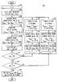
- test setA simplified schematic diagram of a conventional test set configured to perform testing of a wafer for hot-carrier injection (HCI) defects is shown in FIG. 1 , in accordance with an exemplary embodiment of the invention.
- an exemplary wafer 100has a plurality of transistors 102 1 - 102 N , each capable of being probed from an exemplary external test set 104 (greatly simplified in this example).
- test set 104has probes (not shown) that are capable of contacting (probing) individual transistors on the wafer 100 for testing.
- the test set 104has the equivalent of a double-pole, double-throw switch 106 under control of processor 108 .
- the switch 106couples either conventional variable voltage sources V Gstress , V Dstress or conventional variable voltage sources V Gtest , V Dtest (in series with ammeter 110 ) to the gate and drain, respectively, to a selected one of the transistors 102 1 - 102 N being tested, herein referred to as a transistor under test (TUT).
- transistor 102 1is the TUT since it is shown being probed by tester 104 ; it is understood that any one of the transistors 102 1 - 102 N may be the TUT.
- the four conventional variable voltage sourcesare also under the control of the processor 108 .
- Ammeter 110measures the drain current of the TUT when coupled by switch 106 to the TUT. It is understood that the voltage sources V Gstress and V Dstress may be combined. Further, switch 106 may be removed and two variable voltage sources, one coupled to the gate and one coupled to the drain of the TUT, may be used to supply both the stress and test voltages to the TUT. For purposes here, reference herein to a voltage source and the voltage it produces are used interchangeably, e.g., V Dstress refers to both the variable voltage source V Dstress and the voltage supplied thereby.
- the switch 106may be configured to apply variable voltage sources V Gstress and V Dstress to “stress” the TUT (e.g., transistor 102 1 ) with excessive gate and drain voltages, and is configured to apply variable voltage sources V Gtest , V Dtest to test the TUT using voltages equal to or less than voltages which the transistors in the integrated circuit 100 are designed to be operated (hereinafter referred to as Vdd).
- Vddis dependent on the process technology used to fabricate the wafer 100 ; for example, Vdd may be 1.8 volts for a 90 nm process technology, 1.2 volts for 65 nm process technology, etc.
- variable voltage sources V Gstress and V Dstressare generally significantly greater than Vdd and are applied to the TUT for an amount of time to result in a change in the DC operating characteristics of the TUT, as described in the above-referenced JEDEC test standard.
- the amount of time for the initial stress the TUTis about 10 seconds. Subsequent stress times (if subsequent TUT stress needed) typically increase geometrically.
- the voltages of the variable voltage sources V Gtest , V Dtest , V Gstress , and V Dstressmay be determined as described below in connection with FIG. 3 .
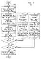
- FIG. 2an exemplary HCI screening test 200 utilizing the test set configuration of FIG. 1 , according to another embodiment of the invention, is illustrated.
- a simple, fast HCI screening testcan be done on an integrated circuit wafer to determine if the transistors thereon are not too susceptible to HCI without the need for a conventional, time consuming, HCI test. If, however, the screening indicates that the integrated circuit wafer might be susceptible to HCI, the wafer may then be subjected to the more definitive and conventional HCI testing, such as the JEDEC technique referred to above.
- one of the transistors 102 1 - 102 N( FIG. 1 ) is chosen to be the TUT (in this example, transistor 102 1 is the TUT) and is probed by the test set 104 . It is understood that this TUT has not been previously stressed.
- the nominal drain current (Id 0 ) of the TUTis measured by ammeter 108 for a gate voltage (V Gtest ) of Vdd (the nominal operating or design voltage of the transistors 102 1 - 102 N ) and a drain voltage (V Dtest ) of, in this example, approximately 0.1 volts.
- V Gtestgate voltage
- V Dtestdrain voltage
- the drain voltage V Dtestis preferably less than a nominal threshold voltage of the transistors 102 1 - 102 N .
- the drain voltagemay be less than 0.1 volts as device geometries get smaller, or greater than 0.1 volts as may be required.
- the TUTis stressed for a nominal 10 seconds by applying approximately equal gate and drain voltages that exceed Vdd.
- the TUTis most stressed when the gate voltage (V Gstress ) and drain voltage (V Dstress ) is the same and significantly exceed Vdd, but it is understood that the gate and drain voltages may be different.
- the desired V Gstress and V Dstress voltagesmay be determined to achieve a desired amount of stress effect in the TUT, the TUT not being significantly susceptible to HCI.
- V Gstress and V Dstressare greater than Vdd and, and in this example, about 1.5 Vdd.
- time periodsmay be used instead of 10 seconds but this time interval makes it possible to use this technique in an HCI screening application on many transistors without a prohibitively long test time while being sufficiently long to result in measurable shifts in the electrical characteristics of the TUT with the voltages given above.
- the drain current (Id 10 ) of the TUT post-stressis measured using the same gate and drain voltages as used in step 204 .
- the change in drain currentis determined and normalized ( ⁇ Id) in step 210 and, in step 212 , the results compared to a drain current change threshold, Ith, to determine if the change in drain current post-stress is so high that further HCI testing is needed (step 214 ) or the wafer passes HCI screening in step 216 and the wafer undergoes further parametric and functional testing.
- the threshold current change Ithis, in this example, approximately 4% but can be another amount depending on the desired lifetime of the wafer 100 and the level of stress applied in step 206 , as is well known in the art.
- the additional HCI testing in step 214may be similar to that disclosed in the JEDEC documents referred to above.
- This additional, conventional HCI testinggenerally comprises repeating the stress and test steps ( 206 - 210 ) for successively longer stress time periods until an accumulated stress time is met or exceeded or the drain current Id 10 differs from the initial current flow Id 0 by greater than a selected amount, e.g., 10%.
- the short HCI screening test 200allows HCI testing of all wafers without the need for the time consuming conventional HCI testing unless the screening test indicates otherwise.
- the process steps 300 illustrated in FIG. 3may be used to determine the desired V Gstress and V Dstress voltages.
- the stress voltagesare selected such that the change in drain current ( ⁇ Id), resulting from the application of the stress voltages, is within a desired range for a “nominal” transistor (i.e., a transistor without significant HCI susceptibility as determined by, for example, a wafer using conventional HCI test described above), here between 2% and 3%.
- a “nominal” transistori.e., a transistor without significant HCI susceptibility as determined by, for example, a wafer using conventional HCI test described above
- the range of 2% to 3%is only exemplary and other values may be used instead.
- the range valuesare chosen to be large enough that a consistently measurable value of current change occurs but is less than the drain current change threshold, Ith, as discussed above in connection with step 212 .
- an integer index value i (1 ⁇ i ⁇ N), used in later steps,is initialized.
- a first transistorsuch as transistor 102 1 in FIG. 1 , is chosen as the TUT. It is understood that this TUT has not been previously stressed.
- Steps 306 , 308 , 310 , and 312are the same as, and correspond to, the steps 204 , 206 , 208 , and 210 , as described above, but, in step 308 , the stress voltages V Gstress , V Dstress are approximately 1.5 Vdd in this example, but other voltages may be used as well.
- the normalized drain current change, ⁇ Idis checked to see if it is within the desired range, here between 2% and 3%. If ⁇ Id is above or below the desired range as determined in steps 314 and 316 , the stress voltages are lowered or increased, respectively, in steps 318 - 332 .
- the index iis incremented and a new, unstressed transistor is chosen as the TUT in step 320 , and the initial (pre-stress) drain current is measured for the new TUT in step 322 .
- step 324the stress voltages are incrementally decreased in step 324 and the stress/test steps 310 - 314 are repeated but using different transistors (as selected in step 320 ) as the TUT until the ⁇ Id is less than or equal to 3%.
- step 326the index i is incremented and a new, unstressed transistor is chosen as the TUT in step 328 , and the initial (pre-stress) drain current is measured for the new TUT in step 330 .
- the stress voltagesare incrementally increased in step 332 and the stress/test steps 310 - 316 are repeated but using different transistors (as selected in step 328 ) as the TUT until the ⁇ Id is more than or equal to 2%. If the ⁇ Id is between 2% and 3% inclusive, then, in step 334 , the final (adjusted) stress voltages may then be used in the HCI screening test 200 , described above, or for the conventional HCI test described above.
- V Gstress and V Dstressare shown as having the same voltage in the embodiments described above, they may have different voltages.
- the gate stress voltage, V Gstressmay be fixed at, for example, Vdd, while V Dstress is adjusted in accordance with the process steps 300 . Further, the order of the steps may be changed and other steps added, as desired.
- the inventionmay be used in any application where hot-carrier injection testing is needed or desired, e.g., in power transistors for power amplifiers, etc.
- each numerical value and rangeshould be interpreted as being approximate as if the word “about” or “approximately” preceded the value of the value or range.
- signals and corresponding nodes, ports, inputs, or outputsmay be referred to by the same name and are interchangeable.
- reference herein to “one embodiment” or “an embodiment”means that a particular feature, structure, or characteristic described in connection with the embodiment can be included in at least one embodiment of the invention.
- the appearances of the phrase “in one embodiment” in various places in the specificationare not necessarily all referring to the same embodiment, nor are separate or alternative embodiments necessarily mutually exclusive of other embodiments. The same applies to the terms “implementation” and “example.”
- Couplerefers to any manner known in the art or later developed in which a signal is allowed to be transferred between two or more elements and the interposition of one or more additional elements is contemplated, although not required. Conversely, the terms “directly coupled,” “directly connected,” etc., imply the absence of such additional elements.
- figure numbers and/or figure reference labels in the claimsis intended to identify one or more possible embodiments of the claimed subject matter in order to facilitate the interpretation of the claims. Such use is not to be construed as necessarily limiting the scope of those claims to the embodiments shown in the corresponding figures.
Landscapes
- Physics & Mathematics (AREA)
- General Physics & Mathematics (AREA)
- Testing Of Individual Semiconductor Devices (AREA)
- Testing Or Measuring Of Semiconductors Or The Like (AREA)
Abstract
Description
- The present invention relates to integrated circuit testing, and, in particular, to hot-carrier injection testing of transistors in integrated circuit wafers or the like.
- As integrated circuit device features continue to shrink beyond 90 nm, the electrical characteristics of transistors with 90 nm and smaller gate lengths have become less than ideal. For example, leakage current and susceptibility to damage of transistor gate dielectric increases as the transistors get smaller. Further, merely using the integrated circuit results in the threshold voltage of the transistors (the voltage applied to the gate of a transistor at which the transistor begins to conduct) in the integrated circuit shifting (aging) that becomes more pronounced with smaller device dimensions. Unfortunately, the shift in threshold voltage is a significant factor in limiting the useful lifetime of an integrated circuit because the threshold voltage shift by the transistors eventually lead to the transistors possibly becoming unresponsive to signals applied to the gates thereof, leading to the functional failure of the integrated circuit.
- One significant contributor to transistor threshold voltage shift is damage to the transistor due to current injection. This phenomenon is known as hot-electron injection or hot-hole injection depending if the affected transistor is an n-channel or p-channel transistor, respectively, and is referred to generically as hot-carrier injection (HCI).
- HCI is a slow process during normal operation but the effect thereof is cumulative over the lifetime of the integrated circuit. Therefore, testing production integrated circuits while still in wafer form requires a technique to accelerate the effects of HCI over a relatively short time period, measuring transistor performance during the testing period, and then extrapolating from changes in the transistor performance to get a projection of the device lifetime. If the projected lifetime is less than a particular value, e.g., 15 years, the wafer is rejected for being overly susceptible to HCI. Various HCI testing techniques have been proposed and adopted, such as that described in “Procedure for Measuring N-Channel MOSFET Hot-Carrier-Induced Degradation Under DC Stress,” JESD28A, published December 2001 (along with corresponding JESD60A for p-channel transistors, published September 2004) by JEDEC Solid State Technology Association, Arlington, Va., USA, both of which are incorporated by reference herein in their entirety. However, the JEDEC test requires multiple hours to perform, an impractical test technique for testing each wafer on a production line. Instead, statistical sampling of selected wafers is used to project device lifetimes of entire production runs (production lots). This may lead to overly optimistic lifetime estimations (with resulting high field failures) or rejecting many wafers that are otherwise satisfactory absent additional, time consuming testing, both of which are costly.
- In one embodiment, the present invention is a method of hot-carrier injection screening a wafer, the method comprising: providing a wafer having at least one MOSFET thereon, the MOSFET having at least a gate, a drain, and a threshold voltage; applying a gate test voltage to the gate and a drain test voltage to the drain of the MOSFET and measuring an initial current flow in the drain; applying, during a stress time period, a gate stress voltage to the gate and a drain stress voltage to the drain of the MOSFET; and applying, at a time subsequent to the stress time period, the gate test voltage to the gate and the drain test voltage to the drain of the MOSFET and measuring a test current flow in the drain. If the test current flow differs from the initial current flow by less than a first selected amount, the wafer passes the hot-carrier injection screen, and the drain test voltage is less than the threshold voltage.
- In another embodiment, the present invention comprises the steps of: selecting one wafer from the plurality of wafers, each wafer having a plurality of MOSFETs thereon and each of the MOSFETs having at least a gate, a drain, and a threshold voltage; selecting one of the plurality of MOSFETs on the selected wafer; applying a gate test voltage to the gate of the selected MOSFET and a drain test voltage to the drain of the selected MOSFET and measuring an initial current flow in the drain of the selected MOSFET; applying, during a stress time period, a gate stress voltage to the gate of the selected MOSFET and a drain stress voltage to the drain of the selected MOSFET; applying, at a time subsequent to the stress time period, the gate test voltage to the gate and the drain test voltage to the drain of the selected MOSFET and measuring a test current flow in the drain of the selected MOSFET; adjusting at least one of the gate and drain stress voltages if the test current flow differs from the initial current flow by less than a selected minimum amount or more than a selected maximum amount. The step of applying, during a stress time period, a gate stress voltage, the step of applying, during a stress time period, a gate stress voltage, and the step of adjusting at least one of the gate and drain stress voltages are repeated with another MOSFET selected from the plurality of MOSFETs until the test current flow differs from the initial current flow greater than the selected minimum amount and less than the selected maximum amount. Preferably, the selected wafer has MOSFETs with acceptable HCI susceptibility. Then at least one of the remaining wafers is hot-carrier injection screened using the stress voltages determined above.
- The aspects, features, and advantages of the present invention will become more fully apparent from the following detailed description, the appended claims, and the accompanying drawings in which like reference numerals identify similar or identical elements.
FIG. 1 is a simplified diagram of an exemplary testing apparatus for performing hot-carrier injection (HCI) screening of transistors on a wafer according to one embodiment of the invention;FIG. 2 is a simplified flowchart illustrating an exemplary HCI screening test utilizing the test apparatus ofFIG. 1 , according to another embodiment of the invention:FIG. 3 is a simplified flowchart illustrating an exemplary process to determine stress voltages for an HCI test utilizing the test apparatus ofFIG. 1 and as used in the HCI screening test ofFIG. 2 , according to another embodiment of the invention.- As is well understood in the art, wafers, such as silicon wafers with diameters of 150 mm or more, have formed therein many integrated circuits laid out across the wafer. Once the wafer is completely fabricated and before the integrated circuits therein are separated from each other (“singulated”), the wafer is subject to extensive testing to determine the functionality of each of the integrated circuits. Prior to the functionality testing, parametric testing of the wafer generally occurs to determine if the processing steps used to form the integrated circuits occurred correctly and within desired tolerances. When a new process is qualified, in addition to conventional parametric tests, the conventional HCI test as described above is done.
- To perform the HCI test, the wafer is placed in a probing station within a conventional testing apparatus (herein a “test set”). The test set, under control of processor, performs the various tests in sequence. A simplified schematic diagram of a conventional test set configured to perform testing of a wafer for hot-carrier injection (HCI) defects is shown in
FIG. 1 , in accordance with an exemplary embodiment of the invention. Here, anexemplary wafer 100 has a plurality of transistors1021-102N, each capable of being probed from an exemplary external test set104 (greatly simplified in this example). As is well understood in the art, test set104 has probes (not shown) that are capable of contacting (probing) individual transistors on thewafer 100 for testing. The test set104 has the equivalent of a double-pole, double-throw switch 106 under control ofprocessor 108. Theswitch 106 couples either conventional variable voltage sources VGstress, VDstressor conventional variable voltage sources VGtest, VDtest(in series with ammeter110) to the gate and drain, respectively, to a selected one of the transistors1021-102Nbeing tested, herein referred to as a transistor under test (TUT). For purposes here,transistor 1021is the TUT since it is shown being probed bytester 104; it is understood that any one of the transistors1021-102Nmay be the TUT. Along with theswitch 106, the four conventional variable voltage sources are also under the control of theprocessor 108.Ammeter 110, readable by theprocessor 108, measures the drain current of the TUT when coupled byswitch 106 to the TUT. It is understood that the voltage sources VGstressand VDstressmay be combined. Further, switch106 may be removed and two variable voltage sources, one coupled to the gate and one coupled to the drain of the TUT, may be used to supply both the stress and test voltages to the TUT. For purposes here, reference herein to a voltage source and the voltage it produces are used interchangeably, e.g., VDstressrefers to both the variable voltage source VDstressand the voltage supplied thereby. - As will be explained in more detail below in connection with
FIG. 2 , theswitch 106 may be configured to apply variable voltage sources VGstressand VDstressto “stress” the TUT (e.g., transistor1021) with excessive gate and drain voltages, and is configured to apply variable voltage sources VGtest, VDtestto test the TUT using voltages equal to or less than voltages which the transistors in theintegrated circuit 100 are designed to be operated (hereinafter referred to as Vdd). Generally, Vdd is dependent on the process technology used to fabricate thewafer 100; for example, Vdd may be 1.8 volts for a 90 nm process technology, 1.2 volts for 65 nm process technology, etc. For HCI testing, the voltages from variable voltage sources VGstressand VDstressare generally significantly greater than Vdd and are applied to the TUT for an amount of time to result in a change in the DC operating characteristics of the TUT, as described in the above-referenced JEDEC test standard. Typically, the amount of time for the initial stress the TUT is about 10 seconds. Subsequent stress times (if subsequent TUT stress needed) typically increase geometrically. The voltages of the variable voltage sources VGtest, VDtest, VGstress, and VDstressmay be determined as described below in connection withFIG. 3 . - Referring to
FIG. 2 , an exemplary HCI screening test200 utilizing the test set configuration ofFIG. 1 , according to another embodiment of the invention, is illustrated. By the judicious choice of stress and test voltages, a simple, fast HCI screening test can be done on an integrated circuit wafer to determine if the transistors thereon are not too susceptible to HCI without the need for a conventional, time consuming, HCI test. If, however, the screening indicates that the integrated circuit wafer might be susceptible to HCI, the wafer may then be subjected to the more definitive and conventional HCI testing, such as the JEDEC technique referred to above. - Beginning with
step 202, one of the transistors1021-102N(FIG. 1 ) is chosen to be the TUT (in this example,transistor 1021is the TUT) and is probed by the test set104. It is understood that this TUT has not been previously stressed. Instep 204, the nominal drain current (Id0) of the TUT is measured byammeter 108 for a gate voltage (VGtest) of Vdd (the nominal operating or design voltage of the transistors1021-102N) and a drain voltage (VDtest) of, in this example, approximately 0.1 volts. The drain voltage VDtestis preferably less than a nominal threshold voltage of the transistors1021-102N. It has been discovered that performing the HCI draincurrent test step 204 using a very low drain voltages has the advantage of enhancing the effects of stress on the TUT and a drain voltage of approximately 0.1 volts has been found to be low enough for 45 nm gate length transistors to give good results without the drain current having so much noise that the test becomes unreliable. It is understood that the drain voltage may be less than 0.1 volts as device geometries get smaller, or greater than 0.1 volts as may be required. - Next, in
step 206, the TUT is stressed for a nominal 10 seconds by applying approximately equal gate and drain voltages that exceed Vdd. Generally, the TUT is most stressed when the gate voltage (VGstress) and drain voltage (VDstress) is the same and significantly exceed Vdd, but it is understood that the gate and drain voltages may be different. As will be discussed in more detail below in connection withFIG. 3 , the desired VGstressand VDstressvoltages may be determined to achieve a desired amount of stress effect in the TUT, the TUT not being significantly susceptible to HCI. Here, VGstressand VDstressare greater than Vdd and, and in this example, about 1.5 Vdd. Other time periods may be used instead of 10 seconds but this time interval makes it possible to use this technique in an HCI screening application on many transistors without a prohibitively long test time while being sufficiently long to result in measurable shifts in the electrical characteristics of the TUT with the voltages given above. - In
step 208, the drain current (Id10) of the TUT post-stress is measured using the same gate and drain voltages as used instep 204. The change in drain current is determined and normalized (ΔId) instep 210 and, instep 212, the results compared to a drain current change threshold, Ith, to determine if the change in drain current post-stress is so high that further HCI testing is needed (step214) or the wafer passes HCI screening instep 216 and the wafer undergoes further parametric and functional testing. The threshold current change Ith is, in this example, approximately 4% but can be another amount depending on the desired lifetime of thewafer 100 and the level of stress applied instep 206, as is well known in the art. - The additional HCI testing in
step 214 may be similar to that disclosed in the JEDEC documents referred to above. This additional, conventional HCI testing generally comprises repeating the stress and test steps (206-210) for successively longer stress time periods until an accumulated stress time is met or exceeded or the drain current Id10 differs from the initial current flow Id0 by greater than a selected amount, e.g., 10%. Advantageously, the short HCI screening test200 allows HCI testing of all wafers without the need for the time consuming conventional HCI testing unless the screening test indicates otherwise. - The process steps300 illustrated in
FIG. 3 may be used to determine the desired VGstressand VDstressvoltages. In this embodiment and because all transistors have some amount of HCI susceptibility, the stress voltages are selected such that the change in drain current (ΔId), resulting from the application of the stress voltages, is within a desired range for a “nominal” transistor (i.e., a transistor without significant HCI susceptibility as determined by, for example, a wafer using conventional HCI test described above), here between 2% and 3%. It is understood that the range of 2% to 3% is only exemplary and other values may be used instead. Generally, the range values are chosen to be large enough that a consistently measurable value of current change occurs but is less than the drain current change threshold, Ith, as discussed above in connection withstep 212. - Beginning with
step 302, an integer index value i (1≦i≦N), used in later steps, is initialized. Instep 304, a first transistor, such astransistor 1021inFIG. 1 , is chosen as the TUT. It is understood that this TUT has not been previously stressed.Steps steps step 308, the stress voltages VGstress, VDstressare approximately 1.5 Vdd in this example, but other voltages may be used as well. Insteps steps step 318, the index i is incremented and a new, unstressed transistor is chosen as the TUT instep 320, and the initial (pre-stress) drain current is measured for the new TUT instep 322. Then the stress voltages are incrementally decreased instep 324 and the stress/test steps310-314 are repeated but using different transistors (as selected in step320) as the TUT until the ΔId is less than or equal to 3%. Similarly, instep 326, the index i is incremented and a new, unstressed transistor is chosen as the TUT instep 328, and the initial (pre-stress) drain current is measured for the new TUT instep 330. Then the stress voltages are incrementally increased instep 332 and the stress/test steps310-316 are repeated but using different transistors (as selected in step328) as the TUT until the ΔId is more than or equal to 2%. If the ΔId is between 2% and 3% inclusive, then, instep 334, the final (adjusted) stress voltages may then be used in the HCI screening test200, described above, or for the conventional HCI test described above. - It is understood that while the stress voltages VGstressand VDstressare shown as having the same voltage in the embodiments described above, they may have different voltages. For example, the gate stress voltage, VGstress, may be fixed at, for example, Vdd, while VDstressis adjusted in accordance with the process steps300. Further, the order of the steps may be changed and other steps added, as desired.
- It is understood that while the embodiment shown herein is for testing an integrated circuit, the invention may be used in any application where hot-carrier injection testing is needed or desired, e.g., in power transistors for power amplifiers, etc.
- For purposes of this description and unless explicitly stated otherwise, each numerical value and range should be interpreted as being approximate as if the word “about” or “approximately” preceded the value of the value or range. Further, signals and corresponding nodes, ports, inputs, or outputs may be referred to by the same name and are interchangeable. Additionally, reference herein to “one embodiment” or “an embodiment” means that a particular feature, structure, or characteristic described in connection with the embodiment can be included in at least one embodiment of the invention. The appearances of the phrase “in one embodiment” in various places in the specification are not necessarily all referring to the same embodiment, nor are separate or alternative embodiments necessarily mutually exclusive of other embodiments. The same applies to the terms “implementation” and “example.”
- Also for purposes of this description, the terms “couple,” “coupling,” “coupled,” “connect,” “connecting,” or “connected,” refer to any manner known in the art or later developed in which a signal is allowed to be transferred between two or more elements and the interposition of one or more additional elements is contemplated, although not required. Conversely, the terms “directly coupled,” “directly connected,” etc., imply the absence of such additional elements.
- It is understood that various changes in the details, materials, and arrangements of the parts which have been described and illustrated in order to explain the nature of this invention may be made by those skilled in the art without departing from the scope of the invention as expressed in the following claims.
- The use of figure numbers and/or figure reference labels in the claims is intended to identify one or more possible embodiments of the claimed subject matter in order to facilitate the interpretation of the claims. Such use is not to be construed as necessarily limiting the scope of those claims to the embodiments shown in the corresponding figures.
- Although the elements in the following method claims, if any, are recited in a particular sequence with corresponding labeling, unless the claim recitations otherwise imply a particular sequence for implementing some or all of those elements, those elements are not necessarily intended to be limited to being implemented in that particular sequence.
Claims (20)
Priority Applications (1)
| Application Number | Priority Date | Filing Date | Title |
|---|---|---|---|
| US12/344,016US7898277B2 (en) | 2008-12-24 | 2008-12-24 | Hot-electronic injection testing of transistors on a wafer |
Applications Claiming Priority (1)
| Application Number | Priority Date | Filing Date | Title |
|---|---|---|---|
| US12/344,016US7898277B2 (en) | 2008-12-24 | 2008-12-24 | Hot-electronic injection testing of transistors on a wafer |
Publications (2)
| Publication Number | Publication Date |
|---|---|
| US20100156454A1true US20100156454A1 (en) | 2010-06-24 |
| US7898277B2 US7898277B2 (en) | 2011-03-01 |
Family
ID=42265071
Family Applications (1)
| Application Number | Title | Priority Date | Filing Date |
|---|---|---|---|
| US12/344,016Expired - Fee RelatedUS7898277B2 (en) | 2008-12-24 | 2008-12-24 | Hot-electronic injection testing of transistors on a wafer |
Country Status (1)
| Country | Link |
|---|---|
| US (1) | US7898277B2 (en) |
Cited By (30)
| Publication number | Priority date | Publication date | Assignee | Title |
|---|---|---|---|---|
| WO2012003359A1 (en)* | 2010-06-30 | 2012-01-05 | Life Technologies Corporation | Methods and apparatus for testing isfet arrays |
| US8217433B1 (en) | 2010-06-30 | 2012-07-10 | Life Technologies Corporation | One-transistor pixel array |
| US8262900B2 (en) | 2006-12-14 | 2012-09-11 | Life Technologies Corporation | Methods and apparatus for measuring analytes using large scale FET arrays |
| US8263336B2 (en) | 2009-05-29 | 2012-09-11 | Life Technologies Corporation | Methods and apparatus for measuring analytes |
| US8264014B2 (en) | 2006-12-14 | 2012-09-11 | Life Technologies Corporation | Methods and apparatus for measuring analytes using large scale FET arrays |
| US8349167B2 (en) | 2006-12-14 | 2013-01-08 | Life Technologies Corporation | Methods and apparatus for detecting molecular interactions using FET arrays |
| US8470164B2 (en) | 2008-06-25 | 2013-06-25 | Life Technologies Corporation | Methods and apparatus for measuring analytes using large scale FET arrays |
| US8653567B2 (en) | 2010-07-03 | 2014-02-18 | Life Technologies Corporation | Chemically sensitive sensor with lightly doped drains |
| US8673627B2 (en) | 2009-05-29 | 2014-03-18 | Life Technologies Corporation | Apparatus and methods for performing electrochemical reactions |
| US8685324B2 (en) | 2010-09-24 | 2014-04-01 | Life Technologies Corporation | Matched pair transistor circuits |
| US8747748B2 (en) | 2012-01-19 | 2014-06-10 | Life Technologies Corporation | Chemical sensor with conductive cup-shaped sensor surface |
| US8776573B2 (en) | 2009-05-29 | 2014-07-15 | Life Technologies Corporation | Methods and apparatus for measuring analytes |
| US8821798B2 (en) | 2012-01-19 | 2014-09-02 | Life Technologies Corporation | Titanium nitride as sensing layer for microwell structure |
| US8858782B2 (en) | 2010-06-30 | 2014-10-14 | Life Technologies Corporation | Ion-sensing charge-accumulation circuits and methods |
| US8936763B2 (en) | 2008-10-22 | 2015-01-20 | Life Technologies Corporation | Integrated sensor arrays for biological and chemical analysis |
| US9080968B2 (en) | 2013-01-04 | 2015-07-14 | Life Technologies Corporation | Methods and systems for point of use removal of sacrificial material |
| US9618475B2 (en) | 2010-09-15 | 2017-04-11 | Life Technologies Corporation | Methods and apparatus for measuring analytes |
| US9823217B2 (en) | 2013-03-15 | 2017-11-21 | Life Technologies Corporation | Chemical device with thin conductive element |
| US9835585B2 (en) | 2013-03-15 | 2017-12-05 | Life Technologies Corporation | Chemical sensor with protruded sensor surface |
| US9841398B2 (en) | 2013-01-08 | 2017-12-12 | Life Technologies Corporation | Methods for manufacturing well structures for low-noise chemical sensors |
| US9970984B2 (en) | 2011-12-01 | 2018-05-15 | Life Technologies Corporation | Method and apparatus for identifying defects in a chemical sensor array |
| US9985624B2 (en) | 2012-05-29 | 2018-05-29 | Life Technologies Corporation | System for reducing noise in a chemical sensor array |
| US10100357B2 (en) | 2013-05-09 | 2018-10-16 | Life Technologies Corporation | Windowed sequencing |
| US10126354B1 (en)* | 2017-06-28 | 2018-11-13 | Globalfoundries Inc. | Assessment of HCI in logic circuits based on AC stress in discrete FETs |
| US10422767B2 (en) | 2013-03-15 | 2019-09-24 | Life Technologies Corporation | Chemical sensor with consistent sensor surface areas |
| US10451585B2 (en) | 2009-05-29 | 2019-10-22 | Life Technologies Corporation | Methods and apparatus for measuring analytes |
| US10458942B2 (en) | 2013-06-10 | 2019-10-29 | Life Technologies Corporation | Chemical sensor array having multiple sensors per well |
| US10605767B2 (en) | 2014-12-18 | 2020-03-31 | Life Technologies Corporation | High data rate integrated circuit with transmitter configuration |
| US11307166B2 (en) | 2010-07-01 | 2022-04-19 | Life Technologies Corporation | Column ADC |
| CN119716451A (en)* | 2024-12-23 | 2025-03-28 | 正芯半导体技术(深圳)有限公司 | A field effect tube intelligent testing method and system based on electrical variables |
Families Citing this family (9)
| Publication number | Priority date | Publication date | Assignee | Title |
|---|---|---|---|---|
| US11339430B2 (en) | 2007-07-10 | 2022-05-24 | Life Technologies Corporation | Methods and apparatus for measuring analytes using large scale FET arrays |
| US8875070B2 (en)* | 2012-10-03 | 2014-10-28 | Lsi Corporation | Breaking up long-channel field effect transistor into smaller segments for reliability modeling |
| US8962366B2 (en) | 2013-01-28 | 2015-02-24 | Life Technologies Corporation | Self-aligned well structures for low-noise chemical sensors |
| US8963216B2 (en) | 2013-03-13 | 2015-02-24 | Life Technologies Corporation | Chemical sensor with sidewall spacer sensor surface |
| US8841217B1 (en) | 2013-03-13 | 2014-09-23 | Life Technologies Corporation | Chemical sensor with protruded sensor surface |
| US9116117B2 (en) | 2013-03-15 | 2015-08-25 | Life Technologies Corporation | Chemical sensor with sidewall sensor surface |
| EP2972279B1 (en) | 2013-03-15 | 2021-10-06 | Life Technologies Corporation | Chemical sensors with consistent sensor surface areas |
| US9054793B2 (en) | 2013-07-19 | 2015-06-09 | International Business Machines Corporation | Structure, system and method for device radio frequency (RF) reliability |
| US10077472B2 (en) | 2014-12-18 | 2018-09-18 | Life Technologies Corporation | High data rate integrated circuit with power management |
Citations (4)
| Publication number | Priority date | Publication date | Assignee | Title |
|---|---|---|---|---|
| US5600578A (en)* | 1993-08-02 | 1997-02-04 | Advanced Micro Devices, Inc. | Test method for predicting hot-carrier induced leakage over time in short-channel IGFETs and products designed in accordance with test results |
| US5999011A (en)* | 1998-03-26 | 1999-12-07 | Taiwan Semiconductor Manufacturing Company | Method of fast testing of hot carrier effects |
| US7106088B2 (en)* | 2005-01-10 | 2006-09-12 | Taiwan Semiconductor Manufacturing Company, Ltd. | Method of predicting high-k semiconductor device lifetime |
| US7750400B2 (en)* | 2008-08-15 | 2010-07-06 | Texas Instruments Incorporated | Integrated circuit modeling, design, and fabrication based on degradation mechanisms |
- 2008
- 2008-12-24USUS12/344,016patent/US7898277B2/ennot_activeExpired - Fee Related
Patent Citations (4)
| Publication number | Priority date | Publication date | Assignee | Title |
|---|---|---|---|---|
| US5600578A (en)* | 1993-08-02 | 1997-02-04 | Advanced Micro Devices, Inc. | Test method for predicting hot-carrier induced leakage over time in short-channel IGFETs and products designed in accordance with test results |
| US5999011A (en)* | 1998-03-26 | 1999-12-07 | Taiwan Semiconductor Manufacturing Company | Method of fast testing of hot carrier effects |
| US7106088B2 (en)* | 2005-01-10 | 2006-09-12 | Taiwan Semiconductor Manufacturing Company, Ltd. | Method of predicting high-k semiconductor device lifetime |
| US7750400B2 (en)* | 2008-08-15 | 2010-07-06 | Texas Instruments Incorporated | Integrated circuit modeling, design, and fabrication based on degradation mechanisms |
Cited By (106)
| Publication number | Priority date | Publication date | Assignee | Title |
|---|---|---|---|---|
| US8540867B2 (en) | 2006-12-14 | 2013-09-24 | Life Technologies Corporation | Methods and apparatus for detecting molecular interactions using FET arrays |
| US8540866B2 (en) | 2006-12-14 | 2013-09-24 | Life Technologies Corporation | Methods and apparatus for detecting molecular interactions using FET arrays |
| US10203300B2 (en) | 2006-12-14 | 2019-02-12 | Life Technologies Corporation | Methods and apparatus for measuring analytes using large scale FET arrays |
| US8262900B2 (en) | 2006-12-14 | 2012-09-11 | Life Technologies Corporation | Methods and apparatus for measuring analytes using large scale FET arrays |
| US8685230B2 (en) | 2006-12-14 | 2014-04-01 | Life Technologies Corporation | Methods and apparatus for high-speed operation of a chemically-sensitive sensor array |
| US8264014B2 (en) | 2006-12-14 | 2012-09-11 | Life Technologies Corporation | Methods and apparatus for measuring analytes using large scale FET arrays |
| US8269261B2 (en) | 2006-12-14 | 2012-09-18 | Life Technologies Corporation | Methods and apparatus for measuring analytes using large scale FET arrays |
| US8293082B2 (en) | 2006-12-14 | 2012-10-23 | Life Technologies Corporation | Methods and apparatus for measuring analytes using large scale FET arrays |
| US8306757B2 (en) | 2006-12-14 | 2012-11-06 | Life Technologies Corporation | Methods and apparatus for measuring analytes using large scale FET arrays |
| US8313639B2 (en) | 2006-12-14 | 2012-11-20 | Life Technologies Corporation | Methods and apparatus for measuring analytes using large scale FET arrays |
| US8313625B2 (en) | 2006-12-14 | 2012-11-20 | Life Technologies Corporation | Methods and apparatus for measuring analytes using large scale FET arrays |
| US8317999B2 (en) | 2006-12-14 | 2012-11-27 | Life Technologies Corporation | Methods and apparatus for measuring analytes using large scale FET arrays |
| US8349167B2 (en) | 2006-12-14 | 2013-01-08 | Life Technologies Corporation | Methods and apparatus for detecting molecular interactions using FET arrays |
| US9989489B2 (en) | 2006-12-14 | 2018-06-05 | Life Technnologies Corporation | Methods for calibrating an array of chemically-sensitive sensors |
| US8415716B2 (en) | 2006-12-14 | 2013-04-09 | Life Technologies Corporation | Chemically sensitive sensors with feedback circuits |
| US8658017B2 (en) | 2006-12-14 | 2014-02-25 | Life Technologies Corporation | Methods for operating an array of chemically-sensitive sensors |
| US9951382B2 (en) | 2006-12-14 | 2018-04-24 | Life Technologies Corporation | Methods and apparatus for measuring analytes using large scale FET arrays |
| US8426898B2 (en) | 2006-12-14 | 2013-04-23 | Life Technologies Corporation | Methods and apparatus for measuring analytes using large scale FET arrays |
| US8426899B2 (en) | 2006-12-14 | 2013-04-23 | Life Technologies Corporation | Methods and apparatus for measuring analytes using large scale FET arrays |
| US8575664B2 (en) | 2006-12-14 | 2013-11-05 | Life Technologies Corporation | Chemically-sensitive sensor array calibration circuitry |
| US9039888B2 (en) | 2006-12-14 | 2015-05-26 | Life Technologies Corporation | Methods and apparatus for detecting molecular interactions using FET arrays |
| US8558288B2 (en) | 2006-12-14 | 2013-10-15 | Life Technologies Corporation | Methods and apparatus for measuring analytes using large scale FET arrays |
| US8435395B2 (en) | 2006-12-14 | 2013-05-07 | Life Technologies Corporation | Methods and apparatus for measuring analytes using large scale FET arrays |
| US8441044B2 (en) | 2006-12-14 | 2013-05-14 | Life Technologies Corporation | Methods for manufacturing low noise chemically-sensitive field effect transistors |
| US8445945B2 (en) | 2006-12-14 | 2013-05-21 | Life Technologies Corporation | Low noise chemically-sensitive field effect transistors |
| US8450781B2 (en) | 2006-12-14 | 2013-05-28 | Life Technologies Corporation | Methods and apparatus for measuring analytes using large scale FET arrays |
| US8540868B2 (en) | 2006-12-14 | 2013-09-24 | Life Technologies Corporation | Methods and apparatus for detecting molecular interactions using FET arrays |
| US8764969B2 (en) | 2006-12-14 | 2014-07-01 | Life Technologies Corporation | Methods for operating chemically sensitive sensors with sample and hold capacitors |
| US8540865B2 (en) | 2006-12-14 | 2013-09-24 | Life Technologies Corporation | Methods and apparatus for detecting molecular interactions using FET arrays |
| US8492800B2 (en) | 2006-12-14 | 2013-07-23 | Life Technologies Corporation | Chemically sensitive sensors with sample and hold capacitors |
| US8492799B2 (en) | 2006-12-14 | 2013-07-23 | Life Technologies Corporation | Methods and apparatus for detecting molecular interactions using FET arrays |
| US8496802B2 (en) | 2006-12-14 | 2013-07-30 | Life Technologies Corporation | Methods for operating chemically-sensitive sample and hold sensors |
| US8502278B2 (en) | 2006-12-14 | 2013-08-06 | Life Technologies Corporation | Chemically-sensitive sample and hold sensors |
| US8519448B2 (en) | 2006-12-14 | 2013-08-27 | Life Technologies Corporation | Chemically-sensitive array with active and reference sensors |
| US8535513B2 (en) | 2006-12-14 | 2013-09-17 | Life Technologies Corporation | Methods and apparatus for measuring analytes using large scale FET arrays |
| US8530941B2 (en) | 2006-12-14 | 2013-09-10 | Life Technologies Corporation | Methods and apparatus for measuring analytes using large scale FET arrays |
| US8524057B2 (en) | 2008-06-25 | 2013-09-03 | Life Technologies Corporation | Methods and apparatus for measuring analytes using large scale FET arrays |
| US8470164B2 (en) | 2008-06-25 | 2013-06-25 | Life Technologies Corporation | Methods and apparatus for measuring analytes using large scale FET arrays |
| US8936763B2 (en) | 2008-10-22 | 2015-01-20 | Life Technologies Corporation | Integrated sensor arrays for biological and chemical analysis |
| US9964515B2 (en) | 2008-10-22 | 2018-05-08 | Life Technologies Corporation | Integrated sensor arrays for biological and chemical analysis |
| US8994076B2 (en) | 2009-05-29 | 2015-03-31 | Life Technologies Corporation | Chemically-sensitive field effect transistor based pixel array with protection diodes |
| US8822205B2 (en) | 2009-05-29 | 2014-09-02 | Life Technologies Corporation | Active chemically-sensitive sensors with source follower amplifier |
| US10451585B2 (en) | 2009-05-29 | 2019-10-22 | Life Technologies Corporation | Methods and apparatus for measuring analytes |
| US8766327B2 (en) | 2009-05-29 | 2014-07-01 | Life Technologies Corporation | Active chemically-sensitive sensors with in-sensor current sources |
| US8592154B2 (en) | 2009-05-29 | 2013-11-26 | Life Technologies Corporation | Methods and apparatus for high speed operation of a chemically-sensitive sensor array |
| US9927393B2 (en) | 2009-05-29 | 2018-03-27 | Life Technologies Corporation | Methods and apparatus for measuring analytes |
| US8592153B1 (en) | 2009-05-29 | 2013-11-26 | Life Technologies Corporation | Methods for manufacturing high capacitance microwell structures of chemically-sensitive sensors |
| US8742469B2 (en) | 2009-05-29 | 2014-06-03 | Life Technologies Corporation | Active chemically-sensitive sensors with correlated double sampling |
| US8776573B2 (en) | 2009-05-29 | 2014-07-15 | Life Technologies Corporation | Methods and apparatus for measuring analytes |
| US8673627B2 (en) | 2009-05-29 | 2014-03-18 | Life Technologies Corporation | Apparatus and methods for performing electrochemical reactions |
| US8263336B2 (en) | 2009-05-29 | 2012-09-11 | Life Technologies Corporation | Methods and apparatus for measuring analytes |
| US8748947B2 (en) | 2009-05-29 | 2014-06-10 | Life Technologies Corporation | Active chemically-sensitive sensors with reset switch |
| US8698212B2 (en) | 2009-05-29 | 2014-04-15 | Life Technologies Corporation | Active chemically-sensitive sensors |
| US8731847B2 (en) | 2010-06-30 | 2014-05-20 | Life Technologies Corporation | Array configuration and readout scheme |
| US8421437B2 (en) | 2010-06-30 | 2013-04-16 | Life Technologies Corporation | Array column integrator |
| US11231451B2 (en) | 2010-06-30 | 2022-01-25 | Life Technologies Corporation | Methods and apparatus for testing ISFET arrays |
| US10641729B2 (en) | 2010-06-30 | 2020-05-05 | Life Technologies Corporation | Column ADC |
| US8217433B1 (en) | 2010-06-30 | 2012-07-10 | Life Technologies Corporation | One-transistor pixel array |
| US8524487B2 (en) | 2010-06-30 | 2013-09-03 | Life Technologies Corporation | One-transistor pixel array with cascoded column circuit |
| US8772698B2 (en) | 2010-06-30 | 2014-07-08 | Life Technologies Corporation | CCD-based multi-transistor active pixel sensor array |
| JP2013533976A (en)* | 2010-06-30 | 2013-08-29 | ライフ テクノロジーズ コーポレーション | Method and apparatus for testing ISFET arrays |
| US8247849B2 (en) | 2010-06-30 | 2012-08-21 | Life Technologies Corporation | Two-transistor pixel array |
| US8415177B2 (en) | 2010-06-30 | 2013-04-09 | Life Technologies Corporation | Two-transistor pixel array |
| US8487790B2 (en) | 2010-06-30 | 2013-07-16 | Life Technologies Corporation | Chemical detection circuit including a serializer circuit |
| US8823380B2 (en) | 2010-06-30 | 2014-09-02 | Life Technologies Corporation | Capacitive charge pump |
| US8858782B2 (en) | 2010-06-30 | 2014-10-14 | Life Technologies Corporation | Ion-sensing charge-accumulation circuits and methods |
| US8455927B2 (en) | 2010-06-30 | 2013-06-04 | Life Technologies Corporation | One-transistor pixel array with cascoded column circuit |
| CN103080739A (en)* | 2010-06-30 | 2013-05-01 | 生命科技公司 | Method and apparatus for testing ISFET arrays |
| US8432150B2 (en) | 2010-06-30 | 2013-04-30 | Life Technologies Corporation | Methods for operating an array column integrator |
| US8415176B2 (en) | 2010-06-30 | 2013-04-09 | Life Technologies Corporation | One-transistor pixel array |
| WO2012003359A1 (en)* | 2010-06-30 | 2012-01-05 | Life Technologies Corporation | Methods and apparatus for testing isfet arrays |
| US9164070B2 (en) | 2010-06-30 | 2015-10-20 | Life Technologies Corporation | Column adc |
| JP2016188867A (en)* | 2010-06-30 | 2016-11-04 | ライフ テクノロジーズ コーポレーション | Methods and apparatus for testing isfet arrays |
| CN103080739B (en)* | 2010-06-30 | 2016-12-21 | 生命科技公司 | Method and apparatus for testing ISFET arrays |
| US8432149B2 (en) | 2010-06-30 | 2013-04-30 | Life Technologies Corporation | Array column integrator |
| CN106932456A (en)* | 2010-06-30 | 2017-07-07 | 生命科技公司 | Method and apparatus for testing ISFET arrays |
| US11307166B2 (en) | 2010-07-01 | 2022-04-19 | Life Technologies Corporation | Column ADC |
| US8653567B2 (en) | 2010-07-03 | 2014-02-18 | Life Technologies Corporation | Chemically sensitive sensor with lightly doped drains |
| US9618475B2 (en) | 2010-09-15 | 2017-04-11 | Life Technologies Corporation | Methods and apparatus for measuring analytes |
| US9958415B2 (en) | 2010-09-15 | 2018-05-01 | Life Technologies Corporation | ChemFET sensor including floating gate |
| US8685324B2 (en) | 2010-09-24 | 2014-04-01 | Life Technologies Corporation | Matched pair transistor circuits |
| US9110015B2 (en) | 2010-09-24 | 2015-08-18 | Life Technologies Corporation | Method and system for delta double sampling |
| US8796036B2 (en) | 2010-09-24 | 2014-08-05 | Life Technologies Corporation | Method and system for delta double sampling |
| US10365321B2 (en) | 2011-12-01 | 2019-07-30 | Life Technologies Corporation | Method and apparatus for identifying defects in a chemical sensor array |
| US10598723B2 (en) | 2011-12-01 | 2020-03-24 | Life Technologies Corporation | Method and apparatus for identifying defects in a chemical sensor array |
| US9970984B2 (en) | 2011-12-01 | 2018-05-15 | Life Technologies Corporation | Method and apparatus for identifying defects in a chemical sensor array |
| US8747748B2 (en) | 2012-01-19 | 2014-06-10 | Life Technologies Corporation | Chemical sensor with conductive cup-shaped sensor surface |
| US8821798B2 (en) | 2012-01-19 | 2014-09-02 | Life Technologies Corporation | Titanium nitride as sensing layer for microwell structure |
| US10404249B2 (en) | 2012-05-29 | 2019-09-03 | Life Technologies Corporation | System for reducing noise in a chemical sensor array |
| US9985624B2 (en) | 2012-05-29 | 2018-05-29 | Life Technologies Corporation | System for reducing noise in a chemical sensor array |
| US9080968B2 (en) | 2013-01-04 | 2015-07-14 | Life Technologies Corporation | Methods and systems for point of use removal of sacrificial material |
| US9852919B2 (en) | 2013-01-04 | 2017-12-26 | Life Technologies Corporation | Methods and systems for point of use removal of sacrificial material |
| US9841398B2 (en) | 2013-01-08 | 2017-12-12 | Life Technologies Corporation | Methods for manufacturing well structures for low-noise chemical sensors |
| US10422767B2 (en) | 2013-03-15 | 2019-09-24 | Life Technologies Corporation | Chemical sensor with consistent sensor surface areas |
| US9835585B2 (en) | 2013-03-15 | 2017-12-05 | Life Technologies Corporation | Chemical sensor with protruded sensor surface |
| US10481124B2 (en) | 2013-03-15 | 2019-11-19 | Life Technologies Corporation | Chemical device with thin conductive element |
| US9823217B2 (en) | 2013-03-15 | 2017-11-21 | Life Technologies Corporation | Chemical device with thin conductive element |
| US11028438B2 (en) | 2013-05-09 | 2021-06-08 | Life Technologies Corporation | Windowed sequencing |
| US10100357B2 (en) | 2013-05-09 | 2018-10-16 | Life Technologies Corporation | Windowed sequencing |
| US10655175B2 (en) | 2013-05-09 | 2020-05-19 | Life Technologies Corporation | Windowed sequencing |
| US10458942B2 (en) | 2013-06-10 | 2019-10-29 | Life Technologies Corporation | Chemical sensor array having multiple sensors per well |
| US10605767B2 (en) | 2014-12-18 | 2020-03-31 | Life Technologies Corporation | High data rate integrated circuit with transmitter configuration |
| US11536688B2 (en) | 2014-12-18 | 2022-12-27 | Life Technologies Corporation | High data rate integrated circuit with transmitter configuration |
| US12196704B2 (en) | 2014-12-18 | 2025-01-14 | Life Technologies Corporation | High data rate integrated circuit with transmitter configuration |
| US10126354B1 (en)* | 2017-06-28 | 2018-11-13 | Globalfoundries Inc. | Assessment of HCI in logic circuits based on AC stress in discrete FETs |
| CN119716451A (en)* | 2024-12-23 | 2025-03-28 | 正芯半导体技术(深圳)有限公司 | A field effect tube intelligent testing method and system based on electrical variables |
Also Published As
| Publication number | Publication date |
|---|---|
| US7898277B2 (en) | 2011-03-01 |
Similar Documents
| Publication | Publication Date | Title |
|---|---|---|
| US7898277B2 (en) | Hot-electronic injection testing of transistors on a wafer | |
| US8283941B2 (en) | Alternating current (AC) stress test circuit, method for evaluating AC stress induced hot carrier injection (HCI) degradation, and test structure for HCI degradation evaluation | |
| CN101796424B (en) | Semiconductor device test system having reduced current leakage | |
| CN102004218B (en) | Chip acceptability testing method | |
| US9778313B2 (en) | Devices under test | |
| JP2001289909A (en) | Failure analyzing method and failure analyzing device for semiconductor integrated circuit | |
| US8362794B2 (en) | Method and system for assessing reliability of integrated circuit | |
| JPH0954140A (en) | Method and apparatus for testing semiconductor integrated circuit | |
| CN115639454A (en) | Threshold voltage monitoring circuit for SiC MOSFET high-temperature reverse bias or high-temperature grid bias test | |
| US7145356B2 (en) | Circuits for transistor testing | |
| US6198301B1 (en) | Method for determining the hot carrier lifetime of a transistor | |
| US6828775B2 (en) | High-impedance mode for precision measurement unit | |
| US8000935B2 (en) | Diagnostic method for root-cause analysis of FET performance variation | |
| US8779796B2 (en) | Method and apparatus for device parameter measurement | |
| JP2008180616A (en) | Test auxiliary circuit and test method for semiconductor device | |
| JP2004045404A (en) | Monitoring circuit element | |
| US6239605B1 (en) | Method to perform IDDQ testing in the presence of high background leakage current | |
| JP2014119379A (en) | Test method for semiconductor transistor | |
| KR102590203B1 (en) | Method and device for wafer-level testing | |
| CN109166842B (en) | Test structure and test method for evaluating gate oxide TDDB polarity difference | |
| WO2022142294A1 (en) | Hot carrier effect degradation performance evaluation method | |
| US7127690B2 (en) | Method and system for defect evaluation using quiescent power plane current (IDDQ) voltage linearity | |
| Pompl et al. | Gate voltage and oxide thickness dependence of progressive wear-out of ultra-thin gate oxides | |
| RU2381514C1 (en) | Method of comparative assessment reliability of batches of semiconductor products | |
| LaRow et al. | Fast TDDB for early reliability monitoring |
Legal Events
| Date | Code | Title | Description |
|---|---|---|---|
| AS | Assignment | Owner name:AGERO SYSTEMS, INC.,PENNSYLVANIA Free format text:ASSIGNMENT OF ASSIGNORS INTEREST;ASSIGNOR:WEIR, BONNIE;REEL/FRAME:022041/0052 Effective date:20081209 Owner name:AGERO SYSTEMS, INC., PENNSYLVANIA Free format text:ASSIGNMENT OF ASSIGNORS INTEREST;ASSIGNOR:WEIR, BONNIE;REEL/FRAME:022041/0052 Effective date:20081209 | |
| AS | Assignment | Owner name:AGERE SYSTEMS, INC.,PENNSYLVANIA Free format text:RE-RECORD TO CORRECT A DOCUMENT PREVIOUSLY RECORDED AT REEL 022041, FRAME 0052. (ASSIGNMENT OF ASSIGNOR'S INTEREST);ASSIGNOR:WEIR, BONNIE;REEL/FRAME:022257/0045 Effective date:20081209 Owner name:AGERE SYSTEMS, INC., PENNSYLVANIA Free format text:RE-RECORD TO CORRECT A DOCUMENT PREVIOUSLY RECORDED AT REEL 022041, FRAME 0052. (ASSIGNMENT OF ASSIGNOR'S INTEREST);ASSIGNOR:WEIR, BONNIE;REEL/FRAME:022257/0045 Effective date:20081209 | |
| STCF | Information on status: patent grant | Free format text:PATENTED CASE | |
| AS | Assignment | Owner name:DEUTSCHE BANK AG NEW YORK BRANCH, AS COLLATERAL AG Free format text:PATENT SECURITY AGREEMENT;ASSIGNORS:LSI CORPORATION;AGERE SYSTEMS LLC;REEL/FRAME:032856/0031 Effective date:20140506 | |
| FPAY | Fee payment | Year of fee payment:4 | |
| AS | Assignment | Owner name:AVAGO TECHNOLOGIES GENERAL IP (SINGAPORE) PTE. LTD Free format text:ASSIGNMENT OF ASSIGNORS INTEREST;ASSIGNOR:AGERE SYSTEMS LLC;REEL/FRAME:035365/0634 Effective date:20140804 | |
| AS | Assignment | Owner name:AGERE SYSTEMS LLC, PENNSYLVANIA Free format text:TERMINATION AND RELEASE OF SECURITY INTEREST IN PATENT RIGHTS (RELEASES RF 032856-0031);ASSIGNOR:DEUTSCHE BANK AG NEW YORK BRANCH, AS COLLATERAL AGENT;REEL/FRAME:037684/0039 Effective date:20160201 Owner name:LSI CORPORATION, CALIFORNIA Free format text:TERMINATION AND RELEASE OF SECURITY INTEREST IN PATENT RIGHTS (RELEASES RF 032856-0031);ASSIGNOR:DEUTSCHE BANK AG NEW YORK BRANCH, AS COLLATERAL AGENT;REEL/FRAME:037684/0039 Effective date:20160201 | |
| AS | Assignment | Owner name:BANK OF AMERICA, N.A., AS COLLATERAL AGENT, NORTH CAROLINA Free format text:PATENT SECURITY AGREEMENT;ASSIGNOR:AVAGO TECHNOLOGIES GENERAL IP (SINGAPORE) PTE. LTD.;REEL/FRAME:037808/0001 Effective date:20160201 Owner name:BANK OF AMERICA, N.A., AS COLLATERAL AGENT, NORTH Free format text:PATENT SECURITY AGREEMENT;ASSIGNOR:AVAGO TECHNOLOGIES GENERAL IP (SINGAPORE) PTE. LTD.;REEL/FRAME:037808/0001 Effective date:20160201 | |
| AS | Assignment | Owner name:AVAGO TECHNOLOGIES GENERAL IP (SINGAPORE) PTE. LTD., SINGAPORE Free format text:TERMINATION AND RELEASE OF SECURITY INTEREST IN PATENTS;ASSIGNOR:BANK OF AMERICA, N.A., AS COLLATERAL AGENT;REEL/FRAME:041710/0001 Effective date:20170119 Owner name:AVAGO TECHNOLOGIES GENERAL IP (SINGAPORE) PTE. LTD Free format text:TERMINATION AND RELEASE OF SECURITY INTEREST IN PATENTS;ASSIGNOR:BANK OF AMERICA, N.A., AS COLLATERAL AGENT;REEL/FRAME:041710/0001 Effective date:20170119 | |
| AS | Assignment | Owner name:BELL SEMICONDUCTOR, LLC, ILLINOIS Free format text:ASSIGNMENT OF ASSIGNORS INTEREST;ASSIGNORS:AVAGO TECHNOLOGIES GENERAL IP (SINGAPORE) PTE. LTD.;BROADCOM CORPORATION;REEL/FRAME:044886/0001 Effective date:20171208 | |
| AS | Assignment | Owner name:CORTLAND CAPITAL MARKET SERVICES LLC, AS COLLATERA Free format text:SECURITY INTEREST;ASSIGNORS:HILCO PATENT ACQUISITION 56, LLC;BELL SEMICONDUCTOR, LLC;BELL NORTHERN RESEARCH, LLC;REEL/FRAME:045216/0020 Effective date:20180124 | |
| FEPP | Fee payment procedure | Free format text:MAINTENANCE FEE REMINDER MAILED (ORIGINAL EVENT CODE: REM.); ENTITY STATUS OF PATENT OWNER: LARGE ENTITY | |
| LAPS | Lapse for failure to pay maintenance fees | Free format text:PATENT EXPIRED FOR FAILURE TO PAY MAINTENANCE FEES (ORIGINAL EVENT CODE: EXP.); ENTITY STATUS OF PATENT OWNER: LARGE ENTITY | |
| STCH | Information on status: patent discontinuation | Free format text:PATENT EXPIRED DUE TO NONPAYMENT OF MAINTENANCE FEES UNDER 37 CFR 1.362 | |
| FP | Lapsed due to failure to pay maintenance fee | Effective date:20190301 | |
| AS | Assignment | Owner name:BELL NORTHERN RESEARCH, LLC, ILLINOIS Free format text:SECURITY INTEREST;ASSIGNOR:CORTLAND CAPITAL MARKET SERVICES LLC;REEL/FRAME:060885/0001 Effective date:20220401 Owner name:BELL SEMICONDUCTOR, LLC, ILLINOIS Free format text:SECURITY INTEREST;ASSIGNOR:CORTLAND CAPITAL MARKET SERVICES LLC;REEL/FRAME:060885/0001 Effective date:20220401 Owner name:HILCO PATENT ACQUISITION 56, LLC, ILLINOIS Free format text:SECURITY INTEREST;ASSIGNOR:CORTLAND CAPITAL MARKET SERVICES LLC;REEL/FRAME:060885/0001 Effective date:20220401 |