US20100148891A1 - Dielectric Waveguide-Microstrip Transition Structure - Google Patents
Dielectric Waveguide-Microstrip Transition StructureDownload PDFInfo
- Publication number
- US20100148891A1 US20100148891A1US12/637,300US63730009AUS2010148891A1US 20100148891 A1US20100148891 A1US 20100148891A1US 63730009 AUS63730009 AUS 63730009AUS 2010148891 A1US2010148891 A1US 2010148891A1
- Authority
- US
- United States
- Prior art keywords
- microstrip
- dielectric waveguide
- dielectric
- slot
- transition structure
- Prior art date
- Legal status (The legal status is an assumption and is not a legal conclusion. Google has not performed a legal analysis and makes no representation as to the accuracy of the status listed.)
- Granted
Links
Images


Classifications
- H—ELECTRICITY
- H01—ELECTRIC ELEMENTS
- H01P—WAVEGUIDES; RESONATORS, LINES, OR OTHER DEVICES OF THE WAVEGUIDE TYPE
- H01P5/00—Coupling devices of the waveguide type
- H01P5/08—Coupling devices of the waveguide type for linking dissimilar lines or devices
- H01P5/10—Coupling devices of the waveguide type for linking dissimilar lines or devices for coupling balanced lines or devices with unbalanced lines or devices
- H01P5/107—Hollow-waveguide/strip-line transitions
Definitions
- the present inventionrelates to a dielectric waveguide-microstrip transition structure for mounting a dielectric waveguide on a printed-wiring board formed with a microstrip line, and a branch circuit using the transition structure.
- This mounting structureis configured such that a coupling electrode pattern formed on a bottom surface of a dielectric waveguide, and a coupling electrode pattern formed on a terminal end of a microstrip, are accommodated within a cavity in opposed relation to each other while providing an air gap therebetween by a spacer, so as to produce electromagnetic coupling therebetween to allow high-frequency energy to be transmitted between the microstrip and the dielectric waveguide.
- a conductor pattern of the microstripis in non-contact with a conductor pattern of the dielectric waveguide, which provides an advantage of being able to perform stable energy transmission without suffering from a contact state between the conductor patterns.
- the conventional mounting structurerequires a relatively long dimension value.
- a length of a conductor pattern to be provided on a bottom surface of the dielectric waveguideis set to 6.6 mm.
- a ratio of the length to the guide wavelengthis in the range of about 0.7 to 1. It is desired to maximally downsize a dielectric waveguide as a component to be mounted on a printed-wiring board. Thus, it is critical challenge to achieve a further downsized mounting structure.
- one object of the present inventionis directed to providing a further downsized structure as compared with the conventional structure using the coupling electrode patterns, while maintaining an influence of displacement between the dielectric waveguide and the microstrip at a low level by means of non-contact coupling.
- a dielectric waveguide-microstrip transition structurewhich has a dielectric waveguide containing a dielectric block and a conductor film covering an entire surface of the dielectric block, except a signal input/output portion, wherein a slot is formed in a bottom surface of the dielectric waveguide to expose the dielectric; a microstrip having an end which is openly terminated and disposed with opposing to and spaced apart from the slot of the dielectric waveguide; and a cavity containing a conductive wall surrounding the end of the microstrip and the slot of the dielectric waveguide, except a part of the microstrip being led out to connect to an external circuit.
- a slotis formed in a bottom surface of a dielectric waveguide.
- a microstripis formed on a printed-wiring board for allowing the dielectric waveguide to be mounted thereon, to have an end openly terminated.
- the dielectric waveguideis mounted on the printed circuit board in such a manner that the slot formed in the bottom surface of the dielectric waveguide is disposed adjacent to and in non-contact with the microstrip with a given distance therebetween.
- a conductive wallis provided to define a cavity so as to accommodate the slot and the end of the microstrip therewithin. A portion of the conductive wall crossing the microstrip (microstrip line) is partially removed to allow the microstrip to pass therethrough.
- the conductive wallis also provided along an outer peripheral edge of an electromagnetic coupling region of the printed-wiring board (printed-circuit board) to define the cavity in cooperation with a top surface of the printed-wiring board and the bottom surface of the dielectric waveguide.
- the terminal end of the microstrip and the slot in the bottom surface of the dielectric waveguideare disposed in adjacent relation to each other to achieve electromagnetic coupling therebetween, so that high-frequency energy can be transmitted between the microstrip and the dielectric waveguide.
- the electromagnetic coupling regionis accommodated within the cavity to minimize leakage and loss of electromagnetic energy.
- only an air layeris interposed in the electromagnetic coupling region, i.e., no substance causing energy loss exists therein, so that energy loss becomes lower.
- the coupling (transition) structurehas no physical contact. This makes it possible to prevent degradation in transmission characteristic due to displacement during mounting, without suffering from a contact state between the dielectric waveguide and the microstrip, and moderate a requirement for positioning accuracy of the dielectric waveguide.
- the conventional coupling electrode patternis required to have a longitudinal length approximately equal to a guide wavelength, as mentioned above. In contract, an electrode pattern to be provided in the dielectric waveguide is only a slot having a minimum size, so that the transition structure can be downsized in its entirety.
- FIG. 1is a perspective view showing a dielectric waveguide for use in a dielectric waveguide-microstrip transition structure according to a first embodiment of the present invention.
- FIG. 2is an exploded perspective view showing the transition structure according to the first embodiment.
- FIG. 3is an exploded perspective view showing a dielectric waveguide-microstrip transition structure according to a second embodiment of the present invention.
- FIG. 4is a perspective view showing the dielectric waveguide-microstrip transition structure according to the second embodiment.
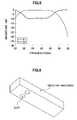
- FIG. 5is a graph showing a characteristic of the transition structure according to the second embodiment.
- FIG. 6is a perspective view showing a dielectric waveguide for use in a dielectric waveguide-microstrip transition structure according to a third embodiment of the present invention.
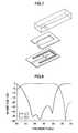
- FIG. 7is an exploded perspective view showing the dielectric waveguide-microstrip transition structure according to the third embodiment.
- FIG. 8is a graph showing a characteristic of the transition structure according to the third embodiment.
- FIG. 9is an exploded perspective view showing one example of modification of the dielectric waveguide-microstrip transition structure according to the third embodiment.
- FIG. 1is a perspective view of a dielectric waveguide 10 for use in a dielectric waveguide-microstrip transition structure according to a first embodiment of the present invention.
- a slot 11is formed in a bottom surface of the dielectric waveguide to extend in a direction perpendicular to a traveling direction of an electromagnetic wave.
- the dielectric waveguidecomprises a dielectric block, and a conductor film formed to expose only a region of a surface of the dielectric block corresponding to the slot, and fully cover the remaining region.
- the dielectric waveguide 10is mounted on a printed-wiring board 14 .
- a microstrip 15is provided on the printed-wiring board to have an end which is openly terminated, and disposed in opposed relation to the bottom surface of the dielectric waveguide with a given distance therebetween.
- a conductive wall 16is provided around the opposed region of the printed-wiring board, and the printed-wiring board 14 is closely fixed to the dielectric waveguide 10 through an interspace created by the conductive wall 16 .
- the microstrip 15 and the dielectric waveguide 10are electromagnetically coupled together through respective conductor patterns thereof to allow an electromagnetic wave to be transmitted therebetween.
- the slot 11is disposed at a position away from an edge of the open terminal end of the microstrip 15 by a distance of about a quarter wavelength, i.e., a position where an electromagnetic field intensity is maximized, to obtain a sufficient coupling.
- a maximum electromagnetic filed intensityis theoretically provided at a position away from the edge of the open terminal end by a distance of a quarter wavelength, the distance actually becomes shorter than a quarter wavelength due to an edge effect of the open terminal end of the microstrip 15 .
- an electromagnetic field intensityis maximized at a position away from a short-circuited terminal end of the dielectric waveguide 10 by a distance of about a half wavelength.
- the slot 11is formed at this position.
- a discontinuous region as a coupling region of a transmission lineis apt to cause large radiation loss and significant degradation in transmission characteristics.
- the coupling (transition) structure in the first embodimentis configured to accommodate the discontinuous region within the cavity defined by the conductive wall to minimize radiation of an electromagnetic field to exterior space.
- FIG. 3is an exploded perspective view showing a dielectric waveguide-microstrip transition structure according to a second embodiment of the present invention.
- FIG. 4shows the transition structure in an assembled state.
- an array of via-holes 37are provided in a printed-wiring board 34 formed with a microstrip 35 , to surround a coupling region, as substitute for a part of the conductive wall provided along the outer peripheral edge of the printed-wiring board in the first embodiment.
- a dielectric waveguide 30is fixed on the printed-wiring board 34 through a spacer 38 serving as a part of the conductive wall.
- the spacer 38may be a member made of an electrically conductive material, or may be a member made of a resin material or a material for printed-wiring boards and formed to have an inner wall plated with a conductor. In either case, the point is to allow an opposed region between the slot and an open terminal end of the microstrip is accommodated by the conductive wall.
- FIG. 5shows a result obtained by calculating an electromagnetic field intensity of the above transition structure using an electromagnetic field simulator.
- a substrate having a thickness of 0.254 mm(relative permittivity: 2.2) was used as the printed-wiring board.
- the dielectric waveguidewas formed to have a cross-sectional size of 4.5 mm ⁇ 2.5 mm (relative permittivity: 4.5), and fixed onto the printed-wiring board through the spacer formed to have a thickness of 0.4 mm.
- the transition structurehad a characteristic where a return loss is about 10 dB in a frequency range of 23 to 27 GHz.
- the slot to be provided in the dielectric waveguidemay be formed in a dumbbell-like shape (generally H shape), as shown in FIG. 6 .
- FIG. 7shows a dielectric waveguide-microstrip transition structure according to a third embodiment of the present invention. As shown in FIG. 7 , in view of impedance matching, an open terminal end of a microstrip in a coupling region is formed in a pattern which comprises a stub portion, and an edge portion extending from the stub portion by a distance of about a quarter wavelength and having a reduced line width, instead of the afore-mentioned simple shape.
- FIG. 7shows a dielectric waveguide-microstrip transition structure according to a third embodiment of the present invention. As shown in FIG. 7 , in view of impedance matching, an open terminal end of a microstrip in a coupling region is formed in a pattern which comprises a stub portion, and an edge portion extending from the stub portion by a distance of about a quarter
- FIG. 8shows a characteristic of the transition structure obtained by optimizing a shape of the slot and a shape of the terminal end of the microstrip, as shown in FIG. 7 .
- This characteristicis a result of calculation using an electromagnetic field simulator.
- a return lossis greater than 24 dB in a frequency range of 23 to 28 GHz, which shows excellent impedance matching.
- An insertion lossis also reduced to 0.3 dB or less.
- one of longitudinally opposite ends of the dielectric waveguideis terminated in a short-circuited manner.
- each of the endsmay be used as an output port without being short-circuited, to allow the transition structure to serve as a branch circuit for distributing an electric power input from the slot.
- the slot in the bottom surface of the dielectric waveguidecan be formed in a symmetrical shape with respect to the two ports.
- the slotmay be disposed at a laterally central position to allow an input from the slot to be distributed half-and-half, in a common phase.
- the present inventioncan be widely used in various coupling structures, such as a coupling structure between a dielectric waveguide and an external circuit, and a branching filter, which are used in a high-frequency band.
Landscapes
- Waveguides (AREA)
Abstract
Description
- This application claims the priority of Japanese Application No. 2008-316570 filed Dec. 12, 2008, the entire content of which is hereby incorporated by reference.
- The present invention relates to a dielectric waveguide-microstrip transition structure for mounting a dielectric waveguide on a printed-wiring board formed with a microstrip line, and a branch circuit using the transition structure.
- As a structure for mounting a dielectric waveguide on a printed-wiring board, there has been known one type disclosed, for example, in JP 4133747B. This mounting structure is configured such that a coupling electrode pattern formed on a bottom surface of a dielectric waveguide, and a coupling electrode pattern formed on a terminal end of a microstrip, are accommodated within a cavity in opposed relation to each other while providing an air gap therebetween by a spacer, so as to produce electromagnetic coupling therebetween to allow high-frequency energy to be transmitted between the microstrip and the dielectric waveguide.
- In the conventional mounting structure, a conductor pattern of the microstrip is in non-contact with a conductor pattern of the dielectric waveguide, which provides an advantage of being able to perform stable energy transmission without suffering from a contact state between the conductor patterns.
- However, the conventional mounting structure requires a relatively long dimension value. For example, in case where the conventional mounting structure is designed on an assumption that a dielectric waveguide having a cross-sectional area of 4.5 mm×2.5 mm is fabricated using a dielectric material with a relative permittivity (dielectric constant) of 4.5, and transition is performed in a frequency band of 23 to 28 GHz, a length of a conductor pattern to be provided on a bottom surface of the dielectric waveguide is set to 6.6 mm. Considering that a guide wavelength of an electromagnetic wave in TE mode to be propagated through the dielectric waveguide is 9.7 mm at 23 GHz and 6.5 mm at 28 GHz, a ratio of the length to the guide wavelength is in the range of about 0.7 to 1. It is desired to maximally downsize a dielectric waveguide as a component to be mounted on a printed-wiring board. Thus, it is critical challenge to achieve a further downsized mounting structure.
- [Patent Document 1] JP 08-148913A
- [Patent Document 2] JP 3493265B
- [Patent Document 3] JP 3517148B
- In a dielectric waveguide-microstrip transition structure for mounting a dielectric waveguide on a printed-wiring board, one object of the present invention is directed to providing a further downsized structure as compared with the conventional structure using the coupling electrode patterns, while maintaining an influence of displacement between the dielectric waveguide and the microstrip at a low level by means of non-contact coupling.
- According to one aspect of the present invention, there is provided a dielectric waveguide-microstrip transition structure which has a dielectric waveguide containing a dielectric block and a conductor film covering an entire surface of the dielectric block, except a signal input/output portion, wherein a slot is formed in a bottom surface of the dielectric waveguide to expose the dielectric; a microstrip having an end which is openly terminated and disposed with opposing to and spaced apart from the slot of the dielectric waveguide; and a cavity containing a conductive wall surrounding the end of the microstrip and the slot of the dielectric waveguide, except a part of the microstrip being led out to connect to an external circuit.
- In a preferred embodiment of the present invention, a slot is formed in a bottom surface of a dielectric waveguide. A microstrip is formed on a printed-wiring board for allowing the dielectric waveguide to be mounted thereon, to have an end openly terminated. The dielectric waveguide is mounted on the printed circuit board in such a manner that the slot formed in the bottom surface of the dielectric waveguide is disposed adjacent to and in non-contact with the microstrip with a given distance therebetween.
- A conductive wall is provided to define a cavity so as to accommodate the slot and the end of the microstrip therewithin. A portion of the conductive wall crossing the microstrip (microstrip line) is partially removed to allow the microstrip to pass therethrough. The conductive wall is also provided along an outer peripheral edge of an electromagnetic coupling region of the printed-wiring board (printed-circuit board) to define the cavity in cooperation with a top surface of the printed-wiring board and the bottom surface of the dielectric waveguide.
- In the dielectric waveguide-microstrip transition structure of the present invention, the terminal end of the microstrip and the slot in the bottom surface of the dielectric waveguide are disposed in adjacent relation to each other to achieve electromagnetic coupling therebetween, so that high-frequency energy can be transmitted between the microstrip and the dielectric waveguide. The electromagnetic coupling region is accommodated within the cavity to minimize leakage and loss of electromagnetic energy. In addition, only an air layer is interposed in the electromagnetic coupling region, i.e., no substance causing energy loss exists therein, so that energy loss becomes lower.
- The coupling (transition) structure has no physical contact. This makes it possible to prevent degradation in transmission characteristic due to displacement during mounting, without suffering from a contact state between the dielectric waveguide and the microstrip, and moderate a requirement for positioning accuracy of the dielectric waveguide. The conventional coupling electrode pattern is required to have a longitudinal length approximately equal to a guide wavelength, as mentioned above. In contract, an electrode pattern to be provided in the dielectric waveguide is only a slot having a minimum size, so that the transition structure can be downsized in its entirety.
FIG. 1 is a perspective view showing a dielectric waveguide for use in a dielectric waveguide-microstrip transition structure according to a first embodiment of the present invention.FIG. 2 is an exploded perspective view showing the transition structure according to the first embodiment.FIG. 3 is an exploded perspective view showing a dielectric waveguide-microstrip transition structure according to a second embodiment of the present invention.FIG. 4 is a perspective view showing the dielectric waveguide-microstrip transition structure according to the second embodiment.FIG. 5 is a graph showing a characteristic of the transition structure according to the second embodiment.FIG. 6 is a perspective view showing a dielectric waveguide for use in a dielectric waveguide-microstrip transition structure according to a third embodiment of the present invention.FIG. 7 is an exploded perspective view showing the dielectric waveguide-microstrip transition structure according to the third embodiment.FIG. 8 is a graph showing a characteristic of the transition structure according to the third embodiment.FIG. 9 is an exploded perspective view showing one example of modification of the dielectric waveguide-microstrip transition structure according to the third embodiment.- With reference to the drawings, the present invention will now be described based on an embodiment thereof.
FIG. 1 is a perspective view of adielectric waveguide 10 for use in a dielectric waveguide-microstrip transition structure according to a first embodiment of the present invention. As shown inFIG. 1 , aslot 11 is formed in a bottom surface of the dielectric waveguide to extend in a direction perpendicular to a traveling direction of an electromagnetic wave. The dielectric waveguide comprises a dielectric block, and a conductor film formed to expose only a region of a surface of the dielectric block corresponding to the slot, and fully cover the remaining region. - As shown in
FIG. 2 , thedielectric waveguide 10 is mounted on a printed-wiring board 14. Amicrostrip 15 is provided on the printed-wiring board to have an end which is openly terminated, and disposed in opposed relation to the bottom surface of the dielectric waveguide with a given distance therebetween. Further, aconductive wall 16 is provided around the opposed region of the printed-wiring board, and the printed-wiring board 14 is closely fixed to thedielectric waveguide 10 through an interspace created by theconductive wall 16. - The
microstrip 15 and thedielectric waveguide 10 are electromagnetically coupled together through respective conductor patterns thereof to allow an electromagnetic wave to be transmitted therebetween. As for a positional relationship between theslot 11 and themicrostrip 15, theslot 11 is disposed at a position away from an edge of the open terminal end of themicrostrip 15 by a distance of about a quarter wavelength, i.e., a position where an electromagnetic field intensity is maximized, to obtain a sufficient coupling. Although a maximum electromagnetic filed intensity is theoretically provided at a position away from the edge of the open terminal end by a distance of a quarter wavelength, the distance actually becomes shorter than a quarter wavelength due to an edge effect of the open terminal end of themicrostrip 15. Further, as for a position where theslot 11 is formed in the bottom surface of thedielectric waveguide 10, an electromagnetic field intensity is maximized at a position away from a short-circuited terminal end of thedielectric waveguide 10 by a distance of about a half wavelength. Thus, theslot 11 is formed at this position. - In high-frequency energy transmission, a discontinuous region as a coupling region of a transmission line is apt to cause large radiation loss and significant degradation in transmission characteristics. The coupling (transition) structure in the first embodiment is configured to accommodate the discontinuous region within the cavity defined by the conductive wall to minimize radiation of an electromagnetic field to exterior space.
FIG. 3 is an exploded perspective view showing a dielectric waveguide-microstrip transition structure according to a second embodiment of the present invention.FIG. 4 shows the transition structure in an assembled state. As shown inFIG. 3 , an array of via-holes 37 are provided in a printed-wiring board 34 formed with amicrostrip 35, to surround a coupling region, as substitute for a part of the conductive wall provided along the outer peripheral edge of the printed-wiring board in the first embodiment. As shown inFIGS. 3 and 4 , adielectric waveguide 30 is fixed on the printed-wiring board 34 through aspacer 38 serving as a part of the conductive wall. Thespacer 38 may be a member made of an electrically conductive material, or may be a member made of a resin material or a material for printed-wiring boards and formed to have an inner wall plated with a conductor. In either case, the point is to allow an opposed region between the slot and an open terminal end of the microstrip is accommodated by the conductive wall.FIG. 5 shows a result obtained by calculating an electromagnetic field intensity of the above transition structure using an electromagnetic field simulator. In this calculation, a substrate having a thickness of 0.254 mm (relative permittivity: 2.2) was used as the printed-wiring board. Further, the dielectric waveguide was formed to have a cross-sectional size of 4.5 mm×2.5 mm (relative permittivity: 4.5), and fixed onto the printed-wiring board through the spacer formed to have a thickness of 0.4 mm. As seen inFIG. 5 , the transition structure had a characteristic where a return loss is about 10 dB in a frequency range of 23 to 27 GHz.- In view of obtaining wider-band transmission characteristics, and improved impedance matching, the slot to be provided in the dielectric waveguide may be formed in a dumbbell-like shape (generally H shape), as shown in
FIG. 6 .FIG. 7 shows a dielectric waveguide-microstrip transition structure according to a third embodiment of the present invention. As shown inFIG. 7 , in view of impedance matching, an open terminal end of a microstrip in a coupling region is formed in a pattern which comprises a stub portion, and an edge portion extending from the stub portion by a distance of about a quarter wavelength and having a reduced line width, instead of the afore-mentioned simple shape.FIG. 8 shows a characteristic of the transition structure obtained by optimizing a shape of the slot and a shape of the terminal end of the microstrip, as shown inFIG. 7 . This characteristic is a result of calculation using an electromagnetic field simulator. As seen inFIG. 8 , a return loss is greater than 24 dB in a frequency range of 23 to 28 GHz, which shows excellent impedance matching. An insertion loss is also reduced to 0.3 dB or less. - In each of the above transition structures, one of longitudinally opposite ends of the dielectric waveguide is terminated in a short-circuited manner. Alternatively, each of the ends may be used as an output port without being short-circuited, to allow the transition structure to serve as a branch circuit for distributing an electric power input from the slot. The slot in the bottom surface of the dielectric waveguide can be formed in a symmetrical shape with respect to the two ports. Thus, as shown in
FIG. 9 , the slot may be disposed at a laterally central position to allow an input from the slot to be distributed half-and-half, in a common phase. - The present invention can be widely used in various coupling structures, such as a coupling structure between a dielectric waveguide and an external circuit, and a branching filter, which are used in a high-frequency band.
Claims (8)
Applications Claiming Priority (2)
| Application Number | Priority Date | Filing Date | Title |
|---|---|---|---|
| JP2008316570AJP5123154B2 (en) | 2008-12-12 | 2008-12-12 | Dielectric waveguide-microstrip conversion structure |
| JP2008-316570 | 2008-12-12 |
Publications (2)
| Publication Number | Publication Date |
|---|---|
| US20100148891A1true US20100148891A1 (en) | 2010-06-17 |
| US8368482B2 US8368482B2 (en) | 2013-02-05 |
Family
ID=41821896
Family Applications (1)
| Application Number | Title | Priority Date | Filing Date |
|---|---|---|---|
| US12/637,300Expired - Fee RelatedUS8368482B2 (en) | 2008-12-12 | 2009-12-14 | Dielectric waveguide-microstrip transition including a cavity coupling structure |
Country Status (5)
| Country | Link |
|---|---|
| US (1) | US8368482B2 (en) |
| EP (1) | EP2197072B1 (en) |
| JP (1) | JP5123154B2 (en) |
| CN (1) | CN101847769B (en) |
| AT (1) | ATE520166T1 (en) |
Cited By (7)
| Publication number | Priority date | Publication date | Assignee | Title |
|---|---|---|---|---|
| US8729979B2 (en) | 2011-01-13 | 2014-05-20 | Toko, Inc. | Input/output coupling structure for dielectric waveguide |
| WO2014104536A1 (en)* | 2012-12-27 | 2014-07-03 | Korea Advanced Institute Of Science And Technology | Low power, high speed multi-channel chip-to-chip interface using dielectric waveguide |
| US20140292438A1 (en)* | 2013-03-29 | 2014-10-02 | Toko, Inc. | Input/Output Structure For Dielectric Waveguide |
| US20150270617A1 (en)* | 2014-03-18 | 2015-09-24 | Peraso Technologies, Inc. | Waveguide adapter plate to facilitate accurate alignment of sectioned waveguide channel in microwave antenna assembly |
| US10014564B2 (en) | 2013-09-13 | 2018-07-03 | Murata Manufacturing Co., Ltd. | Dielectric waveguide resonator and filter comprised of a pair of dielectric blocks having opposing surfaces coupled to each other by a probe |
| EP3267528A4 (en)* | 2015-03-03 | 2018-10-17 | Korea Advanced Institute of Science and Technology | Chip-to-chip interface using microstrip circuit and dielectric waveguide |
| CN113904076A (en)* | 2021-12-13 | 2022-01-07 | 成都雷电微晶科技有限公司 | W-band H-plane probe transition structure with image frequency suppression characteristic |
Families Citing this family (17)
| Publication number | Priority date | Publication date | Assignee | Title |
|---|---|---|---|---|
| US8680936B2 (en)* | 2011-11-18 | 2014-03-25 | Delphi Technologies, Inc. | Surface mountable microwave signal transition block for microstrip to perpendicular waveguide transition |
| RU2486640C1 (en)* | 2012-01-10 | 2013-06-27 | Федеральное государственное унитарное предприятие "Ростовский-на-Дону научно-исследовательский институт радиосвязи" (ФГУП "РНИИРС") | Waveguide-microstrip junction with below-cutoff load |
| KR101323841B1 (en) | 2012-05-31 | 2014-01-27 | 주식회사 만도 | Transition structure including patch antenna and waveguide |
| JPWO2013186968A1 (en)* | 2012-06-11 | 2016-02-01 | 日本電気株式会社 | Electromagnetic wave propagation system, interface device and electromagnetic wave propagation sheet |
| JP6123801B2 (en)* | 2012-06-11 | 2017-05-10 | 日本電気株式会社 | Electromagnetic wave propagation system, interface device and electromagnetic wave propagation sheet |
| KR101375938B1 (en) | 2012-12-27 | 2014-03-21 | 한국과학기술원 | Low power, high speed multi-channel chip-to-chip interface using dielectric waveguide |
| FR3010835B1 (en) | 2013-09-19 | 2015-09-11 | Inst Mines Telecom Telecom Bretagne | JUNCTION DEVICE BETWEEN A PRINTED TRANSMISSION LINE AND A DIELECTRIC WAVEGUIDE |
| US10014566B2 (en) | 2013-10-01 | 2018-07-03 | Sony Semiconductor Solutions Corporation | Connector apparatus and communication system |
| JP2016225894A (en)* | 2015-06-02 | 2016-12-28 | 東光株式会社 | Dielectric waveguide filter and dielectric waveguide duplexer |
| WO2017175776A1 (en)* | 2016-04-08 | 2017-10-12 | 株式会社村田製作所 | Dielectric waveguide input-output structure and dielectric waveguide duplexer provided therewith |
| EP3240101B1 (en)* | 2016-04-26 | 2020-07-29 | Huawei Technologies Co., Ltd. | Radiofrequency interconnection between a printed circuit board and a waveguide |
| US10530047B2 (en)* | 2017-05-24 | 2020-01-07 | Waymo Llc | Broadband waveguide launch designs on single layer PCB |
| DE102019101276A1 (en) | 2019-01-18 | 2020-07-23 | Rosenberger Hochfrequenztechnik Gmbh & Co. Kg | Waveguide arrangement, waveguide transition and use of a waveguide arrangement |
| US20240128994A1 (en)* | 2021-06-29 | 2024-04-18 | Molex, Llc | Transmission system |
| TWI776601B (en)* | 2021-07-22 | 2022-09-01 | 先豐通訊股份有限公司 | Circuit board structure having waveguide and method for manufacturing the same |
| CN114050407B (en)* | 2021-10-28 | 2023-09-26 | 中国科学院空天信息创新研究院 | Waveguide mode excitation structures, methods and applications |
| JP2023139824A (en)* | 2022-03-22 | 2023-10-04 | 株式会社豊田中央研究所 | Electromagnetic wave transmission sheet and connection structure of electromagnetic wave transmission sheet |
Citations (8)
| Publication number | Priority date | Publication date | Assignee | Title |
|---|---|---|---|---|
| US5726664A (en)* | 1994-05-23 | 1998-03-10 | Hughes Electronics | End launched microstrip or stripline to waveguide transition with cavity backed slot fed by T-shaped microstrip line or stripline usable in a missile |
| US5912598A (en)* | 1997-07-01 | 1999-06-15 | Trw Inc. | Waveguide-to-microstrip transition for mmwave and MMIC applications |
| US6081241A (en)* | 1997-05-26 | 2000-06-27 | Telefonaktiebolaget Lm Ericsson | Microwave antenna transmission device having a stripline to waveguide transition via a slot coupling |
| US20020097109A1 (en)* | 2000-12-21 | 2002-07-25 | Du Toit Cornelis Frederik | Waveguide to microstrip transition |
| US6486748B1 (en)* | 1999-02-24 | 2002-11-26 | Trw Inc. | Side entry E-plane probe waveguide to microstrip transition |
| US6614332B2 (en)* | 2001-05-28 | 2003-09-02 | Murata Manufacturing Co., Ltd. | Transmission line, integrated circuit, and transmitter receiver |
| US6677837B2 (en)* | 2001-07-17 | 2004-01-13 | Toko, Inc. | Dielectric waveguide filter and mounting structure thereof |
| US7132905B2 (en)* | 2003-11-07 | 2006-11-07 | Toko Inc. | Input/output coupling structure for dielectric waveguide having conductive coupling patterns separated by a spacer |
Family Cites Families (11)
| Publication number | Priority date | Publication date | Assignee | Title |
|---|---|---|---|---|
| JPS5193848A (en)* | 1975-02-17 | 1976-08-17 | ||
| JP2738776B2 (en) | 1990-09-27 | 1998-04-08 | キヤノン株式会社 | Image forming device |
| JPH08148913A (en)* | 1994-11-18 | 1996-06-07 | Fujitsu General Ltd | Waveguide-microstrip line converter |
| US5793263A (en)* | 1996-05-17 | 1998-08-11 | University Of Massachusetts | Waveguide-microstrip transmission line transition structure having an integral slot and antenna coupling arrangement |
| JP3493265B2 (en)* | 1996-09-30 | 2004-02-03 | 京セラ株式会社 | Dielectric waveguide line and wiring board |
| JP3517148B2 (en) | 1999-03-01 | 2004-04-05 | 京セラ株式会社 | Connection structure between dielectric waveguide line and high-frequency line conductor |
| JP4079660B2 (en)* | 2001-04-27 | 2008-04-23 | 日本電気株式会社 | High frequency circuit board |
| JP4074839B2 (en) | 2003-07-04 | 2008-04-16 | 東光株式会社 | Input / output coupling structure of dielectric waveguide resonator and oscillator using it |
| FR2869723A1 (en)* | 2004-04-29 | 2005-11-04 | Thomson Licensing Sa | NON-CONTACT TRANSITION ELEMENT BETWEEN A WAVEGUIDE AND A MOCRORUBAN LINE |
| US7498896B2 (en)* | 2007-04-27 | 2009-03-03 | Delphi Technologies, Inc. | Waveguide to microstrip line coupling apparatus |
| WO2008146535A1 (en)* | 2007-05-31 | 2008-12-04 | Kyocera Corporation | Terminator |
- 2008
- 2008-12-12JPJP2008316570Apatent/JP5123154B2/ennot_activeExpired - Fee Related
- 2009
- 2009-11-30ATAT09014854Tpatent/ATE520166T1/ennot_activeIP Right Cessation
- 2009-11-30EPEP09014854Apatent/EP2197072B1/ennot_activeNot-in-force
- 2009-12-14CNCN200910258380.8Apatent/CN101847769B/ennot_activeExpired - Fee Related
- 2009-12-14USUS12/637,300patent/US8368482B2/ennot_activeExpired - Fee Related
Patent Citations (8)
| Publication number | Priority date | Publication date | Assignee | Title |
|---|---|---|---|---|
| US5726664A (en)* | 1994-05-23 | 1998-03-10 | Hughes Electronics | End launched microstrip or stripline to waveguide transition with cavity backed slot fed by T-shaped microstrip line or stripline usable in a missile |
| US6081241A (en)* | 1997-05-26 | 2000-06-27 | Telefonaktiebolaget Lm Ericsson | Microwave antenna transmission device having a stripline to waveguide transition via a slot coupling |
| US5912598A (en)* | 1997-07-01 | 1999-06-15 | Trw Inc. | Waveguide-to-microstrip transition for mmwave and MMIC applications |
| US6486748B1 (en)* | 1999-02-24 | 2002-11-26 | Trw Inc. | Side entry E-plane probe waveguide to microstrip transition |
| US20020097109A1 (en)* | 2000-12-21 | 2002-07-25 | Du Toit Cornelis Frederik | Waveguide to microstrip transition |
| US6614332B2 (en)* | 2001-05-28 | 2003-09-02 | Murata Manufacturing Co., Ltd. | Transmission line, integrated circuit, and transmitter receiver |
| US6677837B2 (en)* | 2001-07-17 | 2004-01-13 | Toko, Inc. | Dielectric waveguide filter and mounting structure thereof |
| US7132905B2 (en)* | 2003-11-07 | 2006-11-07 | Toko Inc. | Input/output coupling structure for dielectric waveguide having conductive coupling patterns separated by a spacer |
Cited By (11)
| Publication number | Priority date | Publication date | Assignee | Title |
|---|---|---|---|---|
| US8729979B2 (en) | 2011-01-13 | 2014-05-20 | Toko, Inc. | Input/output coupling structure for dielectric waveguide |
| WO2014104536A1 (en)* | 2012-12-27 | 2014-07-03 | Korea Advanced Institute Of Science And Technology | Low power, high speed multi-channel chip-to-chip interface using dielectric waveguide |
| US20140292438A1 (en)* | 2013-03-29 | 2014-10-02 | Toko, Inc. | Input/Output Structure For Dielectric Waveguide |
| US9437913B2 (en)* | 2013-03-29 | 2016-09-06 | Toko, Inc. | Dielectric waveguide comprised of a dielectric block and a dielectric plate sandwiching an input/output feeder line |
| US10014564B2 (en) | 2013-09-13 | 2018-07-03 | Murata Manufacturing Co., Ltd. | Dielectric waveguide resonator and filter comprised of a pair of dielectric blocks having opposing surfaces coupled to each other by a probe |
| US20150270617A1 (en)* | 2014-03-18 | 2015-09-24 | Peraso Technologies, Inc. | Waveguide adapter plate to facilitate accurate alignment of sectioned waveguide channel in microwave antenna assembly |
| US9577340B2 (en)* | 2014-03-18 | 2017-02-21 | Peraso Technologies Inc. | Waveguide adapter plate to facilitate accurate alignment of sectioned waveguide channel in microwave antenna assembly |
| EP3267528A4 (en)* | 2015-03-03 | 2018-10-17 | Korea Advanced Institute of Science and Technology | Chip-to-chip interface using microstrip circuit and dielectric waveguide |
| US10686241B2 (en) | 2015-03-03 | 2020-06-16 | Korea Advanced Institute Of Science And Technology | Board-to-board interconnect apparatus including a microstrip circuit connected by a waveguide, where a bandwidth of a frequency band is adjustable |
| US11289788B2 (en) | 2015-03-03 | 2022-03-29 | Korea Advanced Institute Of Science And Technology | Board-to-board interconnect apparatus including microstrip circuits connected by a waveguide, wherein a bandwidth of a frequency band is adjustable |
| CN113904076A (en)* | 2021-12-13 | 2022-01-07 | 成都雷电微晶科技有限公司 | W-band H-plane probe transition structure with image frequency suppression characteristic |
Also Published As
| Publication number | Publication date |
|---|---|
| JP5123154B2 (en) | 2013-01-16 |
| JP2010141644A (en) | 2010-06-24 |
| CN101847769A (en) | 2010-09-29 |
| EP2197072B1 (en) | 2011-08-10 |
| US8368482B2 (en) | 2013-02-05 |
| ATE520166T1 (en) | 2011-08-15 |
| EP2197072A1 (en) | 2010-06-16 |
| CN101847769B (en) | 2014-07-09 |
Similar Documents
| Publication | Publication Date | Title |
|---|---|---|
| US8368482B2 (en) | Dielectric waveguide-microstrip transition including a cavity coupling structure | |
| CN113169457B (en) | Ridge gap waveguide and multilayer antenna array including the same | |
| KR101089195B1 (en) | Input / output coupling structure of dielectric waveguide | |
| US6677837B2 (en) | Dielectric waveguide filter and mounting structure thereof | |
| JP4568235B2 (en) | Transmission line converter | |
| EP0848447A2 (en) | Transmission circuit using strip line in three dimensions | |
| KR101158559B1 (en) | Contact-free element of transition between a waveguide and a microstrip line | |
| WO2017158020A1 (en) | Adapter structure with waveguide channels | |
| US20200388899A1 (en) | Microstrip-to-waveguide transition and radio assembly | |
| JP3965762B2 (en) | Triplate line interlayer connector | |
| US20120182093A1 (en) | Microwave filter | |
| US6956449B2 (en) | Quadrature hybrid low loss directional coupler | |
| JP2003174305A (en) | Transmission line and transmitter-receiver | |
| US20250062519A1 (en) | Ultra wideband board-to-board transitions for stripline rf transmission lines | |
| JP2000252712A (en) | Connection structure between dielectric waveguide line and high-frequency line conductor | |
| JP4105017B2 (en) | Waveguide type dielectric filter | |
| US8115565B2 (en) | Dual polarized waveguide feed arrangement with symmetrically tapered structures | |
| TW200403884A (en) | Circuit switcher, high frequency module and communication device | |
| JP4105011B2 (en) | Waveguide type dielectric filter | |
| EP3523853A1 (en) | A waveguide feed | |
| JP7561015B2 (en) | Waveguide structure and horn antenna | |
| US20250226582A1 (en) | Antenna module | |
| US8487711B2 (en) | Microstrip to waveguide transition arrangement having a transitional part with a border contact section | |
| JP2023168665A (en) | High frequency circuit and radar device | |
| JP4542531B2 (en) | Transmission mode conversion structure |
Legal Events
| Date | Code | Title | Description |
|---|---|---|---|
| AS | Assignment | Owner name:TOKO, INC.,JAPAN Free format text:ASSIGNMENT OF ASSIGNORS INTEREST;ASSIGNOR:SANO, KAZUHISA;REEL/FRAME:024076/0012 Effective date:20091109 Owner name:TOKO, INC., JAPAN Free format text:ASSIGNMENT OF ASSIGNORS INTEREST;ASSIGNOR:SANO, KAZUHISA;REEL/FRAME:024076/0012 Effective date:20091109 | |
| STCF | Information on status: patent grant | Free format text:PATENTED CASE | |
| FPAY | Fee payment | Year of fee payment:4 | |
| FEPP | Fee payment procedure | Free format text:PAYOR NUMBER ASSIGNED (ORIGINAL EVENT CODE: ASPN); ENTITY STATUS OF PATENT OWNER: LARGE ENTITY | |
| AS | Assignment | Owner name:MURATA MANUFACTURING CO., LTD., JAPAN Free format text:ASSIGNMENT OF ASSIGNORS INTEREST;ASSIGNOR:TOKO, INC.;REEL/FRAME:043164/0038 Effective date:20170508 | |
| MAFP | Maintenance fee payment | Free format text:PAYMENT OF MAINTENANCE FEE, 8TH YEAR, LARGE ENTITY (ORIGINAL EVENT CODE: M1552); ENTITY STATUS OF PATENT OWNER: LARGE ENTITY Year of fee payment:8 | |
| FEPP | Fee payment procedure | Free format text:MAINTENANCE FEE REMINDER MAILED (ORIGINAL EVENT CODE: REM.); ENTITY STATUS OF PATENT OWNER: LARGE ENTITY | |
| LAPS | Lapse for failure to pay maintenance fees | Free format text:PATENT EXPIRED FOR FAILURE TO PAY MAINTENANCE FEES (ORIGINAL EVENT CODE: EXP.); ENTITY STATUS OF PATENT OWNER: LARGE ENTITY | |
| STCH | Information on status: patent discontinuation | Free format text:PATENT EXPIRED DUE TO NONPAYMENT OF MAINTENANCE FEES UNDER 37 CFR 1.362 | |
| FP | Lapsed due to failure to pay maintenance fee | Effective date:20250205 |