US20100148351A1 - Method of packaging integrated circuit devices using preformed carrier - Google Patents
Method of packaging integrated circuit devices using preformed carrierDownload PDFInfo
- Publication number
- US20100148351A1 US20100148351A1US12/704,423US70442310AUS2010148351A1US 20100148351 A1US20100148351 A1US 20100148351A1US 70442310 AUS70442310 AUS 70442310AUS 2010148351 A1US2010148351 A1US 2010148351A1
- Authority
- US
- United States
- Prior art keywords
- integrated circuit
- substrate
- recess
- chip
- circuit chip
- Prior art date
- Legal status (The legal status is an assumption and is not a legal conclusion. Google has not performed a legal analysis and makes no representation as to the accuracy of the status listed.)
- Granted
Links
- 238000000034methodMethods0.000titleabstractdescription32
- 238000004806packaging method and processMethods0.000titleabstractdescription8
- 239000000758substrateSubstances0.000claimsabstractdescription45
- 239000000463materialSubstances0.000claimsdescription19
- 239000000853adhesiveSubstances0.000claimsdescription14
- 230000001070adhesive effectEffects0.000claimsdescription14
- 239000008393encapsulating agentSubstances0.000claimsdescription8
- 238000000465mouldingMethods0.000claimsdescription6
- 239000004593EpoxySubstances0.000claimsdescription5
- 239000002390adhesive tapeSubstances0.000claimsdescription4
- 150000001875compoundsChemical class0.000claimsdescription4
- 230000008878couplingEffects0.000abstractdescription5
- 238000010168coupling processMethods0.000abstractdescription5
- 238000005859coupling reactionMethods0.000abstractdescription5
- 238000004377microelectronicMethods0.000description7
- 238000001746injection mouldingMethods0.000description4
- 238000012858packaging processMethods0.000description4
- 229910000679solderInorganic materials0.000description3
- 238000001721transfer mouldingMethods0.000description3
- 238000013461designMethods0.000description2
- 238000011161developmentMethods0.000description2
- 230000000873masking effectEffects0.000description2
- 238000012986modificationMethods0.000description2
- 230000004048modificationEffects0.000description2
- XUIMIQQOPSSXEZ-UHFFFAOYSA-NSiliconChemical compound[Si]XUIMIQQOPSSXEZ-UHFFFAOYSA-N0.000description1
- 230000003466anti-cipated effectEffects0.000description1
- 238000003491arrayMethods0.000description1
- 230000015572biosynthetic processEffects0.000description1
- 238000005229chemical vapour depositionMethods0.000description1
- 238000004140cleaningMethods0.000description1
- 238000010276constructionMethods0.000description1
- 238000005336crackingMethods0.000description1
- 238000005520cutting processMethods0.000description1
- -1e.g.Substances0.000description1
- 230000000694effectsEffects0.000description1
- 238000005530etchingMethods0.000description1
- 239000007924injectionSubstances0.000description1
- 238000000206photolithographyMethods0.000description1
- 238000007747platingMethods0.000description1
- 229920001690polydopaminePolymers0.000description1
- 229910052710siliconInorganic materials0.000description1
- 239000010703siliconSubstances0.000description1
- 238000007740vapor depositionMethods0.000description1
- 239000002699waste materialSubstances0.000description1
Images


Classifications
- H—ELECTRICITY
- H01—ELECTRIC ELEMENTS
- H01L—SEMICONDUCTOR DEVICES NOT COVERED BY CLASS H10
- H01L23/00—Details of semiconductor or other solid state devices
- H01L23/12—Mountings, e.g. non-detachable insulating substrates
- H01L23/13—Mountings, e.g. non-detachable insulating substrates characterised by the shape
- H—ELECTRICITY
- H01—ELECTRIC ELEMENTS
- H01L—SEMICONDUCTOR DEVICES NOT COVERED BY CLASS H10
- H01L23/00—Details of semiconductor or other solid state devices
- H01L23/48—Arrangements for conducting electric current to or from the solid state body in operation, e.g. leads, terminal arrangements ; Selection of materials therefor
- H01L23/488—Arrangements for conducting electric current to or from the solid state body in operation, e.g. leads, terminal arrangements ; Selection of materials therefor consisting of soldered or bonded constructions
- H01L23/498—Leads, i.e. metallisations or lead-frames on insulating substrates, e.g. chip carriers
- H01L23/49833—Leads, i.e. metallisations or lead-frames on insulating substrates, e.g. chip carriers the chip support structure consisting of a plurality of insulating substrates
- H—ELECTRICITY
- H01—ELECTRIC ELEMENTS
- H01L—SEMICONDUCTOR DEVICES NOT COVERED BY CLASS H10
- H01L2224/00—Indexing scheme for arrangements for connecting or disconnecting semiconductor or solid-state bodies and methods related thereto as covered by H01L24/00
- H01L2224/01—Means for bonding being attached to, or being formed on, the surface to be connected, e.g. chip-to-package, die-attach, "first-level" interconnects; Manufacturing methods related thereto
- H01L2224/26—Layer connectors, e.g. plate connectors, solder or adhesive layers; Manufacturing methods related thereto
- H01L2224/31—Structure, shape, material or disposition of the layer connectors after the connecting process
- H01L2224/32—Structure, shape, material or disposition of the layer connectors after the connecting process of an individual layer connector
- H01L2224/321—Disposition
- H01L2224/32151—Disposition the layer connector connecting between a semiconductor or solid-state body and an item not being a semiconductor or solid-state body, e.g. chip-to-substrate, chip-to-passive
- H01L2224/32221—Disposition the layer connector connecting between a semiconductor or solid-state body and an item not being a semiconductor or solid-state body, e.g. chip-to-substrate, chip-to-passive the body and the item being stacked
- H01L2224/32225—Disposition the layer connector connecting between a semiconductor or solid-state body and an item not being a semiconductor or solid-state body, e.g. chip-to-substrate, chip-to-passive the body and the item being stacked the item being non-metallic, e.g. insulating substrate with or without metallisation
- H—ELECTRICITY
- H01—ELECTRIC ELEMENTS
- H01L—SEMICONDUCTOR DEVICES NOT COVERED BY CLASS H10
- H01L2224/00—Indexing scheme for arrangements for connecting or disconnecting semiconductor or solid-state bodies and methods related thereto as covered by H01L24/00
- H01L2224/01—Means for bonding being attached to, or being formed on, the surface to be connected, e.g. chip-to-package, die-attach, "first-level" interconnects; Manufacturing methods related thereto
- H01L2224/42—Wire connectors; Manufacturing methods related thereto
- H01L2224/47—Structure, shape, material or disposition of the wire connectors after the connecting process
- H01L2224/48—Structure, shape, material or disposition of the wire connectors after the connecting process of an individual wire connector
- H01L2224/481—Disposition
- H01L2224/48151—Connecting between a semiconductor or solid-state body and an item not being a semiconductor or solid-state body, e.g. chip-to-substrate, chip-to-passive
- H01L2224/48221—Connecting between a semiconductor or solid-state body and an item not being a semiconductor or solid-state body, e.g. chip-to-substrate, chip-to-passive the body and the item being stacked
- H01L2224/48225—Connecting between a semiconductor or solid-state body and an item not being a semiconductor or solid-state body, e.g. chip-to-substrate, chip-to-passive the body and the item being stacked the item being non-metallic, e.g. insulating substrate with or without metallisation
- H01L2224/4824—Connecting between the body and an opposite side of the item with respect to the body
- H—ELECTRICITY
- H01—ELECTRIC ELEMENTS
- H01L—SEMICONDUCTOR DEVICES NOT COVERED BY CLASS H10
- H01L2224/00—Indexing scheme for arrangements for connecting or disconnecting semiconductor or solid-state bodies and methods related thereto as covered by H01L24/00
- H01L2224/01—Means for bonding being attached to, or being formed on, the surface to be connected, e.g. chip-to-package, die-attach, "first-level" interconnects; Manufacturing methods related thereto
- H01L2224/42—Wire connectors; Manufacturing methods related thereto
- H01L2224/47—Structure, shape, material or disposition of the wire connectors after the connecting process
- H01L2224/49—Structure, shape, material or disposition of the wire connectors after the connecting process of a plurality of wire connectors
- H01L2224/491—Disposition
- H01L2224/4912—Layout
- H01L2224/49175—Parallel arrangements
- H—ELECTRICITY
- H01—ELECTRIC ELEMENTS
- H01L—SEMICONDUCTOR DEVICES NOT COVERED BY CLASS H10
- H01L2224/00—Indexing scheme for arrangements for connecting or disconnecting semiconductor or solid-state bodies and methods related thereto as covered by H01L24/00
- H01L2224/73—Means for bonding being of different types provided for in two or more of groups H01L2224/10, H01L2224/18, H01L2224/26, H01L2224/34, H01L2224/42, H01L2224/50, H01L2224/63, H01L2224/71
- H01L2224/732—Location after the connecting process
- H01L2224/73201—Location after the connecting process on the same surface
- H01L2224/73215—Layer and wire connectors
- H—ELECTRICITY
- H01—ELECTRIC ELEMENTS
- H01L—SEMICONDUCTOR DEVICES NOT COVERED BY CLASS H10
- H01L23/00—Details of semiconductor or other solid state devices
- H01L23/48—Arrangements for conducting electric current to or from the solid state body in operation, e.g. leads, terminal arrangements ; Selection of materials therefor
- H01L23/488—Arrangements for conducting electric current to or from the solid state body in operation, e.g. leads, terminal arrangements ; Selection of materials therefor consisting of soldered or bonded constructions
- H01L23/498—Leads, i.e. metallisations or lead-frames on insulating substrates, e.g. chip carriers
- H01L23/49811—Additional leads joined to the metallisation on the insulating substrate, e.g. pins, bumps, wires, flat leads
- H01L23/49816—Spherical bumps on the substrate for external connection, e.g. ball grid arrays [BGA]
- H—ELECTRICITY
- H01—ELECTRIC ELEMENTS
- H01L—SEMICONDUCTOR DEVICES NOT COVERED BY CLASS H10
- H01L24/00—Arrangements for connecting or disconnecting semiconductor or solid-state bodies; Methods or apparatus related thereto
- H01L24/01—Means for bonding being attached to, or being formed on, the surface to be connected, e.g. chip-to-package, die-attach, "first-level" interconnects; Manufacturing methods related thereto
- H01L24/42—Wire connectors; Manufacturing methods related thereto
- H01L24/47—Structure, shape, material or disposition of the wire connectors after the connecting process
- H01L24/48—Structure, shape, material or disposition of the wire connectors after the connecting process of an individual wire connector
- H—ELECTRICITY
- H01—ELECTRIC ELEMENTS
- H01L—SEMICONDUCTOR DEVICES NOT COVERED BY CLASS H10
- H01L24/00—Arrangements for connecting or disconnecting semiconductor or solid-state bodies; Methods or apparatus related thereto
- H01L24/01—Means for bonding being attached to, or being formed on, the surface to be connected, e.g. chip-to-package, die-attach, "first-level" interconnects; Manufacturing methods related thereto
- H01L24/42—Wire connectors; Manufacturing methods related thereto
- H01L24/47—Structure, shape, material or disposition of the wire connectors after the connecting process
- H01L24/49—Structure, shape, material or disposition of the wire connectors after the connecting process of a plurality of wire connectors
- H—ELECTRICITY
- H01—ELECTRIC ELEMENTS
- H01L—SEMICONDUCTOR DEVICES NOT COVERED BY CLASS H10
- H01L2924/00—Indexing scheme for arrangements or methods for connecting or disconnecting semiconductor or solid-state bodies as covered by H01L24/00
- H01L2924/0001—Technical content checked by a classifier
- H01L2924/00014—Technical content checked by a classifier the subject-matter covered by the group, the symbol of which is combined with the symbol of this group, being disclosed without further technical details
- H—ELECTRICITY
- H01—ELECTRIC ELEMENTS
- H01L—SEMICONDUCTOR DEVICES NOT COVERED BY CLASS H10
- H01L2924/00—Indexing scheme for arrangements or methods for connecting or disconnecting semiconductor or solid-state bodies as covered by H01L24/00
- H01L2924/01—Chemical elements
- H01L2924/01078—Platinum [Pt]
- H—ELECTRICITY
- H01—ELECTRIC ELEMENTS
- H01L—SEMICONDUCTOR DEVICES NOT COVERED BY CLASS H10
- H01L2924/00—Indexing scheme for arrangements or methods for connecting or disconnecting semiconductor or solid-state bodies as covered by H01L24/00
- H01L2924/10—Details of semiconductor or other solid state devices to be connected
- H01L2924/11—Device type
- H01L2924/14—Integrated circuits
- H01L2924/143—Digital devices
- H01L2924/1433—Application-specific integrated circuit [ASIC]
- H—ELECTRICITY
- H01—ELECTRIC ELEMENTS
- H01L—SEMICONDUCTOR DEVICES NOT COVERED BY CLASS H10
- H01L2924/00—Indexing scheme for arrangements or methods for connecting or disconnecting semiconductor or solid-state bodies as covered by H01L24/00
- H01L2924/15—Details of package parts other than the semiconductor or other solid state devices to be connected
- H01L2924/151—Die mounting substrate
- H01L2924/1515—Shape
- H01L2924/15153—Shape the die mounting substrate comprising a recess for hosting the device
- H—ELECTRICITY
- H01—ELECTRIC ELEMENTS
- H01L—SEMICONDUCTOR DEVICES NOT COVERED BY CLASS H10
- H01L2924/00—Indexing scheme for arrangements or methods for connecting or disconnecting semiconductor or solid-state bodies as covered by H01L24/00
- H01L2924/15—Details of package parts other than the semiconductor or other solid state devices to be connected
- H01L2924/151—Die mounting substrate
- H01L2924/153—Connection portion
- H01L2924/1531—Connection portion the connection portion being formed only on the surface of the substrate opposite to the die mounting surface
- H01L2924/15311—Connection portion the connection portion being formed only on the surface of the substrate opposite to the die mounting surface being a ball array, e.g. BGA
- H—ELECTRICITY
- H01—ELECTRIC ELEMENTS
- H01L—SEMICONDUCTOR DEVICES NOT COVERED BY CLASS H10
- H01L2924/00—Indexing scheme for arrangements or methods for connecting or disconnecting semiconductor or solid-state bodies as covered by H01L24/00
- H01L2924/15—Details of package parts other than the semiconductor or other solid state devices to be connected
- H01L2924/181—Encapsulation
Definitions
- the present inventiongenerally relates to the field of packaging integrated circuit devices, and, more particularly, to a method of packaging integrated circuit devices using a preformed carrier.
- Microelectronic devicesgenerally have a die (i.e., a chip) that includes integrated circuitry having a high density of very small components.
- a large number of dieare manufactured on a single wafer using many different processes that may be repeated at various stages (e.g., implanting, doping, photolithography, chemical vapor deposition, plasma vapor deposition, plating, planarizing, etching, etc.).
- the dietypically include an array of very small bond pads electrically coupled to the integrated circuitry.
- the bond padsare the external electrical contacts on the die through which the supply voltage, signals, etc. are transmitted to and from the integrated circuitry.
- the dieare then separated from one another (i.e., singulated) by backgrinding and cutting the wafer. After the wafer has been singulated, the individual die are typically “packaged” to couple the bond pads to a larger array of electrical terminals that can be more easily coupled to the various power supply lines, signal lines and ground lines.
- the present inventionis directed to a device and various methods that may solve, or at least reduce, some or all of the aforementioned problems.
- the present inventionis generally directed to a method of packaging integrated circuit devices using a preformed carrier.
- the methodcomprises providing a carrier having a plurality of pockets formed therein, positioning an integrated circuit chip and a substrate in each of the plurality of pockets and conductively coupling the integrated circuit chip and the substrate in each of the plurality of pockets to one another.
- the methodcomprises providing a carrier having a plurality of pockets formed therein, each of the pockets including a first recess and a second recess.
- the methodfurther comprises, for each of the pockets, positioning an integrated circuit chip in the first recess and positioning a substrate in the second recess and conductively coupling the integrated circuit chip and the substrate in each of the plurality of pockets to one another.
- the present inventionis also directed to a packaged integrated circuit device.
- the devicecomprises a preformed body having an integrated circuit chip and a substrate positioned within the preformed body, the integrated chip and the substrate being conductively coupled to one another.
- the devicecomprises a preformed body comprising a first recess and a second recess, an integrated circuit chip positioned in the first recess, a substrate positioned within the second recess and a plurality of wire bonds conductively coupled to the integrated circuit chip and the substrate.
- FIG. 1is a perspective view of one illustrative embodiment of a premolded chip carrier in accordance with one illustrative aspect of the present invention
- FIG. 2is a perspective, cross-sectional view of an illustrative pocket, a plurality of which may be formed in the carrier depicted in FIG. 1 ;
- FIG. 3is a cross-sectional view depicting one illustrative embodiment of a packaged integrated circuit device in accordance with one embodiment of the present invention
- FIG. 4is a plan view depicting one illustrative technique for conductively coupling an integrated circuit chip and a substrate in accordance with one illustrative aspect of the present invention
- FIGS. 5A-5Idepict one illustrative process flow that may be practiced in forming a packaged integrated circuit device in accordance with one aspect of the present invention
- FIG. 6is a cross-sectional view depicting an optional external support structure that may be employed with the present invention.
- FIG. 7is a cross-sectional view of a packaged integrated circuit device after it has been trimmed in accordance with another aspect of the present invention.
- FIG. 1is a perspective view of one illustrative embodiment of a premolded carrier 10 with a plurality of preformed pockets 12 for integrated circuit chips in accordance with one aspect of the present invention.
- the carrier 10may be formed by a variety of known techniques, e.g., transfer or injection molding.
- FIG. 2is a cross-sectional, perspective view of one of the illustrative pockets 12 depicted in FIG. 1 .
- the illustrative pockets 12 depicted hereincomprise a body 11 having a first recess or pocket 14 that is adapted to receive an integrated circuit (IC) chip and a second recess or pocket 16 that is adapted to have a substrate positioned therein.
- ICintegrated circuit
- the body 11further comprises a mold cap 13 having a thickness 15 that may vary depending upon the particular application.
- the thickness 15may range from approximately 0.1-0.2 mm.
- laser masking on the mold cap 13will require that the thickness 15 be at least about 0.05 mm.
- the thickness 15may be less than that value.
- the present inventionhas broad applicability and thus should not be considered to be limited to the illustrative embodiments disclosed herein.
- the size, number and configuration of the preformed pockets 12 and the recesses 14 , 16 formed in the carrier 10may vary depending upon the particular application. In the illustrative embodiment depicted in FIG.
- the carrier 10contains sixteen illustrative pockets 12 , although more or less may be provided in practicing the present invention. Additionally, the size and configuration of the first and second recesses 14 , 16 may also vary depending upon the particular application. Thus, the illustrative examples depicted herein should not be considered a limitation of the present invention.
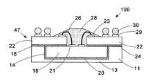
- FIG. 3is a cross-sectional view of a packaged integrated circuit device 100 in accordance with one aspect of the present invention.
- FIG. 4is a partial plan view of the device depicted in FIG. 3 .
- an integrated circuit (IC) chip or die 18is secured within the first recess 14 by adhesive material 20
- a substrate 22is secured within the second recess 16 by adhesive material 24 .
- the present inventionmay be employed with any type of integrated circuit device, e.g., a memory device, a microprocessor, an application specific integrated circuit (ASIC), etc. More than one integrated circuit chip may also be positioned in the first recess 14 depending upon the particular application.
- the substrate 22may be any type of structure that is commonly connected to an IC chip 18 .
- the substrate 22may be an interposer, a printed circuit board, flex tape, a silicon interposer, etc.
- the adhesive material 20 , 24may be an adhesive paste or an adhesive tape which are both well known in the art.
- a plurality of wire bonds 26are conductively coupled to bond pads 21 on the IC chip 18 and to bond pads 23 on the substrate 22 using known wire attach techniques. As seen in FIG. 4 , a slot 37 is formed in the substrate 22 to allow attachment of the wire bonds 26 to the underlying IC chip 18 .
- An encapsulant material 28is formed to over the wire bonds 26 and associated bond pads 21 , 23 .
- the encapsulant material 28may be any of a variety of materials, e.g., epoxy or molding compound, and it may be formed using a variety of techniques, e.g., injection or transfer molding.
- Also depicted in FIG. 3are a plurality of solder balls 30 that are coupled to bond pads 29 formed on the substrate 22 using known techniques.
- the solder balls 30may be employed to conductively couple the packaged integrated circuit device to a structure (not shown), such as a printed circuit board, a motherboard, a module board, etc., using known techniques.
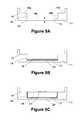
- FIG. 5Adepicts one illustrative pocket 12 that is initially formed as part of the carrier 10 .
- the pocket 12comprises a first recess 14 and a second recess 16 .
- the first recess 14is defined by a bottom surface 14 a and sidewalls 14 b
- the second recess 16is defined by a ledge 16 a and sidewalls 16 b .
- the shape and configuration of the first and second recesses 14 , 16may vary depending upon the particular application.
- the thickness 15 of the mold cap 13may vary depending upon the particular application.
- the mold cap 13may be sufficiently thick to withstand the rigors of the packaging process.
- this external support structure 27may be a tape carrier that is adhesively coupled to the bottom surface 25 of the mold cap 13 .
- the physical size, e.g., thickness, of the external support structure 27may be varied to provide sufficient support to the mold cap 13 for the anticipated loading conditions to be experienced during the packaging process.
- the optional external support structure 27will not be depicted in any additional drawings so as not to obscure the present invention.
- an adhesive material 20.e.g., a die attach paste, is dispensed into the first recess 14 .
- the IC chip or die 18is then mounted into the first recess 14 , as show in FIG. 5C , using traditional pick and place techniques.
- the IC chip 18could be secured in the first recess 14 using an adhesive tape.
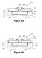
- additional adhesive material 24e.g., adhesive paste
- the substrate 22is positioned within the second recess 16 and attached to the adhesive material 24 using known techniques.
- wire bonds 26are conductively coupled to the bond pads 21 (on the IC chip 18 ) and bond pads 23 (on the substrate 22 ) to conductively couple the substrate 22 to the IC chip 18 .
- the wire bonds 26may be attached using a variety of known attachment techniques and materials.
- the substrate 22is provided with a wire bond slot 37 (see FIG. 4 ) to enable the attachment of the wire bonds 26 .
- an encapsulant material 28e.g., epoxy, is formed to cover the wire bonds 26 and the bond pads 21 , 23 .
- the encapsulant material 28may be formed by a variety of known techniques and it may be formed using a variety of known techniques.
- the bond pads 29 on the substrate 22are exposed and solder balls 30 are formed on the bond pads 29 using traditional techniques.
- the structure depicted in FIG. 5Hmay now be trimmed to the final desired package size.
- the packaged devicemay be trimmed along line 46 wherein the body 11 is along the exposed edge 47 of the packaged integrated circuit device 100 , as shown in FIG. 3 .
- the packaged device 100may be trimmed along the lines 48 , in which case the substrate 22 is on the exposed edge 47 of the device 100 , as shown in FIG. 7 .
- the IC chip 18 and the substrate 22may be pre-assembled or coupled together to form a pre-assembled unit. Thereafter, that pre-assembled unit may be positioned and secured within the pocket 12 of the pre-molded body 11 .
- the present inventionmay reduce warpage as compared to packaging methodologies employing organic substrates.
- the premolded carrier 10 depicted hereinis relatively rigid and flat, thus enabling the carrier 10 to endure the rigors of the packaging process.
- the thickness 15 of the mold cap 13may be reduced as compared to prior art packaging designs, thereby resulting in a thinner packaged integrated circuit device which occupies less space.
- the carrier 10can be formed with a larger number of pockets 12 , thereby resulting in less mold cleaning operations and reduced mold waste. Since the premold pocket 12 is employed, there will be less loss due to encapsulant formation activities as only the wire bond slot 37 may require transfer or injection molding. At least some of these and other benefits may be obtained through use of the present invention.
Landscapes
- Physics & Mathematics (AREA)
- Condensed Matter Physics & Semiconductors (AREA)
- General Physics & Mathematics (AREA)
- Engineering & Computer Science (AREA)
- Computer Hardware Design (AREA)
- Microelectronics & Electronic Packaging (AREA)
- Power Engineering (AREA)
- Encapsulation Of And Coatings For Semiconductor Or Solid State Devices (AREA)
- Structures Or Materials For Encapsulating Or Coating Semiconductor Devices Or Solid State Devices (AREA)
Abstract
Description
- This application is a divisional of U.S. application Ser. No. 11/277,292 filed Mar. 23, 2006, which is incorporated herein by reference in its entirety.
- 1. Field of the Invention
- The present invention generally relates to the field of packaging integrated circuit devices, and, more particularly, to a method of packaging integrated circuit devices using a preformed carrier.
- 2. Description of the Related Art
- Microelectronic devices generally have a die (i.e., a chip) that includes integrated circuitry having a high density of very small components. In a typical process, a large number of die are manufactured on a single wafer using many different processes that may be repeated at various stages (e.g., implanting, doping, photolithography, chemical vapor deposition, plasma vapor deposition, plating, planarizing, etching, etc.). The die typically include an array of very small bond pads electrically coupled to the integrated circuitry. The bond pads are the external electrical contacts on the die through which the supply voltage, signals, etc. are transmitted to and from the integrated circuitry. The die are then separated from one another (i.e., singulated) by backgrinding and cutting the wafer. After the wafer has been singulated, the individual die are typically “packaged” to couple the bond pads to a larger array of electrical terminals that can be more easily coupled to the various power supply lines, signal lines and ground lines.
- Electronic products require packaged microelectronic devices to have an extremely high density of components in a very limited space. For example, the space available for memory devices, processors, displays and other microelectronic components is quite limited in cell phones, PDAs, portable computers and many other products. As such, there is a strong drive to reduce the height of a packaged microelectronic device and the surface area or “footprint” of a microelectronic device on a printed circuit board. Reducing the size of a microelectronic device is difficult because high performance microelectronic devices generally have more bond pads, which result in larger ball/grid arrays and thus larger footprints.
- There are many techniques of packaging integrated circuit devices. Most involve conductively coupling a substrate, e.g., a printed circuit board, an interposer, etc., to the integrated circuit chip using a plurality of wire bonds. Thereafter, the chip and substrate are positioned in a mold and an injection molding process is typically performed to encapsulate the chip and the substrate in an encapsulant material, e.g., molding compound, epoxy, etc. The process described above, while acceptable in many applications, still suffers from said drawbacks. For example, products may have to be scrapped due to problems encountered in the molding process, e.g., voids. Moreover, the process described above may be very labor-intensive in that it requires that the molding apparatus be frequently cleaned.
- The present invention is directed to a device and various methods that may solve, or at least reduce, some or all of the aforementioned problems.
- The following presents a simplified summary of the invention in order to provide a basic understanding of some aspects of the invention. This summary is not an exhaustive overview of the invention. It is not intended to identify key or critical elements of the invention or to delineate the scope of the invention. Its sole purpose is to present some concepts in a simplified form as a prelude to the more detailed description that is discussed later.
- The present invention is generally directed to a method of packaging integrated circuit devices using a preformed carrier. In one illustrative embodiment, the method comprises providing a carrier having a plurality of pockets formed therein, positioning an integrated circuit chip and a substrate in each of the plurality of pockets and conductively coupling the integrated circuit chip and the substrate in each of the plurality of pockets to one another.
- In another illustrative embodiment, the method comprises providing a carrier having a plurality of pockets formed therein, each of the pockets including a first recess and a second recess. The method further comprises, for each of the pockets, positioning an integrated circuit chip in the first recess and positioning a substrate in the second recess and conductively coupling the integrated circuit chip and the substrate in each of the plurality of pockets to one another.
- The present invention is also directed to a packaged integrated circuit device. In one illustrative embodiment, the device comprises a preformed body having an integrated circuit chip and a substrate positioned within the preformed body, the integrated chip and the substrate being conductively coupled to one another.
- In another illustrative embodiment, the device comprises a preformed body comprising a first recess and a second recess, an integrated circuit chip positioned in the first recess, a substrate positioned within the second recess and a plurality of wire bonds conductively coupled to the integrated circuit chip and the substrate.
- The invention may be understood by reference to the following description taken in conjunction with the accompanying drawings, in which like reference numerals identify like elements, and in which:
FIG. 1 is a perspective view of one illustrative embodiment of a premolded chip carrier in accordance with one illustrative aspect of the present invention;FIG. 2 is a perspective, cross-sectional view of an illustrative pocket, a plurality of which may be formed in the carrier depicted inFIG. 1 ;FIG. 3 is a cross-sectional view depicting one illustrative embodiment of a packaged integrated circuit device in accordance with one embodiment of the present invention;FIG. 4 is a plan view depicting one illustrative technique for conductively coupling an integrated circuit chip and a substrate in accordance with one illustrative aspect of the present invention;FIGS. 5A-5I depict one illustrative process flow that may be practiced in forming a packaged integrated circuit device in accordance with one aspect of the present invention;FIG. 6 is a cross-sectional view depicting an optional external support structure that may be employed with the present invention; andFIG. 7 is a cross-sectional view of a packaged integrated circuit device after it has been trimmed in accordance with another aspect of the present invention.- While the invention is susceptible to various modifications and alternative forms, specific embodiments thereof have been shown by way of example in the drawings and are herein described in detail. It should be understood, however, that the description herein of specific embodiments is not intended to limit the invention to the particular forms disclosed, but on the contrary, the intention is to cover all modifications, equivalents, and alternatives falling within the spirit and scope of the invention as defined by the appended claims.
- Illustrative embodiments of the invention are described below. In the interest of clarity, not all features of an actual implementation are described in this specification. It will of course be appreciated that in the development of any such actual embodiment, numerous implementation-specific decisions must be made to achieve the developers' specific goals, such as compliance with system-related and business-related constraints, which will vary from one implementation to another. Moreover, it will be appreciated that such a development effort might be complex and time-consuming, but would nevertheless be a routine undertaking for those of ordinary skill in the art having the benefit of this disclosure.
- The present invention will now be described with reference to the attached figures. Various regions and structures of a packaged integrated circuit device are depicted in the drawings. For purposes of clarity and explanation, the relative sizes of the various features depicted in the drawings may be exaggerated or reduced as compared to the size of those features or structures on real-world packaged devices. Nevertheless, the attached drawings are included to describe and explain illustrative examples of the present invention. The words and phrases used herein should be understood and interpreted to have a meaning consistent with the understanding of those words and phrases by those skilled in the relevant art. No special definition of a term or phrase, i.e., a definition that is different from the ordinary and customary meaning as understood by those skilled in the art, is intended to be implied by consistent usage of the term or phrase herein. To the extent that a term or phrase is intended to have a special meaning, i.e., a meaning other than that understood by skilled artisans, such a special definition will be explicitly set forth in the specification in a definitional manner that directly and unequivocally provides the special definition for the term or phrase.
FIG. 1 is a perspective view of one illustrative embodiment of apremolded carrier 10 with a plurality ofpreformed pockets 12 for integrated circuit chips in accordance with one aspect of the present invention. Thecarrier 10 may be formed by a variety of known techniques, e.g., transfer or injection molding.FIG. 2 is a cross-sectional, perspective view of one of theillustrative pockets 12 depicted inFIG. 1 . As shown inFIG. 2 , theillustrative pockets 12 depicted herein comprise abody 11 having a first recess orpocket 14 that is adapted to receive an integrated circuit (IC) chip and a second recess orpocket 16 that is adapted to have a substrate positioned therein. Thebody 11 further comprises amold cap 13 having athickness 15 that may vary depending upon the particular application. For example, thethickness 15 may range from approximately 0.1-0.2 mm. Typically, laser masking on themold cap 13 will require that thethickness 15 be at least about 0.05 mm. However, if laser masking is not required, thethickness 15 may be less than that value. After a complete reading of the present application, those skilled in the art will appreciate that the present invention has broad applicability and thus should not be considered to be limited to the illustrative embodiments disclosed herein. For example, the size, number and configuration of the preformed pockets12 and therecesses carrier 10 may vary depending upon the particular application. In the illustrative embodiment depicted inFIG. 1 , thecarrier 10 contains sixteenillustrative pockets 12, although more or less may be provided in practicing the present invention. Additionally, the size and configuration of the first andsecond recesses FIG. 3 is a cross-sectional view of a packagedintegrated circuit device 100 in accordance with one aspect of the present invention.FIG. 4 is a partial plan view of the device depicted inFIG. 3 . As shown in these drawings, an integrated circuit (IC) chip or die18 is secured within thefirst recess 14 byadhesive material 20, and asubstrate 22 is secured within thesecond recess 16 byadhesive material 24. Of course, the present invention may be employed with any type of integrated circuit device, e.g., a memory device, a microprocessor, an application specific integrated circuit (ASIC), etc. More than one integrated circuit chip may also be positioned in thefirst recess 14 depending upon the particular application. Thesubstrate 22 may be any type of structure that is commonly connected to anIC chip 18. For example, thesubstrate 22 may be an interposer, a printed circuit board, flex tape, a silicon interposer, etc. Theadhesive material wire bonds 26 are conductively coupled tobond pads 21 on theIC chip 18 and to bondpads 23 on thesubstrate 22 using known wire attach techniques. As seen inFIG. 4 , aslot 37 is formed in thesubstrate 22 to allow attachment of thewire bonds 26 to theunderlying IC chip 18.- An
encapsulant material 28 is formed to over thewire bonds 26 and associatedbond pads encapsulant material 28 may be any of a variety of materials, e.g., epoxy or molding compound, and it may be formed using a variety of techniques, e.g., injection or transfer molding. Also depicted inFIG. 3 are a plurality ofsolder balls 30 that are coupled tobond pads 29 formed on thesubstrate 22 using known techniques. Ultimately, thesolder balls 30 may be employed to conductively couple the packaged integrated circuit device to a structure (not shown), such as a printed circuit board, a motherboard, a module board, etc., using known techniques. - One illustrative process flow for forming a packaged
integrated circuit device 100 in accordance with the present invention will now be described with reference toFIGS. 5A-5I .FIG. 5A depicts oneillustrative pocket 12 that is initially formed as part of thecarrier 10. As shown therein, thepocket 12 comprises afirst recess 14 and asecond recess 16. In the depicted embodiment, thefirst recess 14 is defined by abottom surface 14aandsidewalls 14b, and thesecond recess 16 is defined by aledge 16aandsidewalls 16b. Of course, the shape and configuration of the first andsecond recesses - As indicated previously, the
thickness 15 of themold cap 13 may vary depending upon the particular application. For many applications, themold cap 13 may be sufficiently thick to withstand the rigors of the packaging process. In some case, it may be desirable to add an optional additional external support structure27 (seeFIG. 6 ) to reduce or eliminate the chances of themold cap 13 cracking or breaking during the chip packaging process. For example, thisexternal support structure 27 may be a tape carrier that is adhesively coupled to thebottom surface 25 of themold cap 13. The physical size, e.g., thickness, of theexternal support structure 27 may be varied to provide sufficient support to themold cap 13 for the anticipated loading conditions to be experienced during the packaging process. For ease of explanation, the optionalexternal support structure 27 will not be depicted in any additional drawings so as not to obscure the present invention. - In
FIG. 5B , anadhesive material 20, .e.g., a die attach paste, is dispensed into thefirst recess 14. The IC chip or die18 is then mounted into thefirst recess 14, as show inFIG. 5C , using traditional pick and place techniques. Of course, if desired, theIC chip 18 could be secured in thefirst recess 14 using an adhesive tape. - Next, as shown in
FIG. 5D , additionaladhesive material 24, e.g., adhesive paste, is positioned above theIC chip 18 and in thesecond recess 16. Then, as shown inFIG. 5E , thesubstrate 22 is positioned within thesecond recess 16 and attached to theadhesive material 24 using known techniques. - Thereafter, as shown in
FIG. 5F ,wire bonds 26 are conductively coupled to the bond pads21 (on the IC chip18) and bond pads23 (on the substrate22) to conductively couple thesubstrate 22 to theIC chip 18. The wire bonds26 may be attached using a variety of known attachment techniques and materials. Note that thesubstrate 22 is provided with a wire bond slot37 (seeFIG. 4 ) to enable the attachment of the wire bonds26. - Next, as shown in
FIG. 5G , anencapsulant material 28, e.g., epoxy, is formed to cover thewire bonds 26 and thebond pads encapsulant material 28 may be formed by a variety of known techniques and it may be formed using a variety of known techniques. - Thereafter, as shown in
FIG. 5H , thebond pads 29 on thesubstrate 22 are exposed andsolder balls 30 are formed on thebond pads 29 using traditional techniques. The structure depicted inFIG. 5H may now be trimmed to the final desired package size. For example, as shown inFIG. 5I , the packaged device may be trimmed alongline 46 wherein thebody 11 is along the exposededge 47 of the packagedintegrated circuit device 100, as shown inFIG. 3 . Alternatively, the packageddevice 100 may be trimmed along thelines 48, in which case thesubstrate 22 is on the exposededge 47 of thedevice 100, as shown inFIG. 7 . - As an alternative, the
IC chip 18 and thesubstrate 22 may be pre-assembled or coupled together to form a pre-assembled unit. Thereafter, that pre-assembled unit may be positioned and secured within thepocket 12 of thepre-molded body 11. - Use of the present invention may provide many significant benefits. For example, the present invention may reduce warpage as compared to packaging methodologies employing organic substrates. The
premolded carrier 10 depicted herein is relatively rigid and flat, thus enabling thecarrier 10 to endure the rigors of the packaging process. Using the present technique, thethickness 15 of themold cap 13 may be reduced as compared to prior art packaging designs, thereby resulting in a thinner packaged integrated circuit device which occupies less space. Thecarrier 10 can be formed with a larger number ofpockets 12, thereby resulting in less mold cleaning operations and reduced mold waste. Since thepremold pocket 12 is employed, there will be less loss due to encapsulant formation activities as only thewire bond slot 37 may require transfer or injection molding. At least some of these and other benefits may be obtained through use of the present invention. - The particular embodiments disclosed above are illustrative only, as the invention may be modified and practiced in different but equivalent manners apparent to those skilled in the art having the benefit of the teachings herein. For example, the process steps set forth above may be performed in a different order. Furthermore, no limitations are intended to the details of construction or design herein shown, other than as described in the claims below. It is therefore evident that the particular embodiments disclosed above may be altered or modified and all such variations are considered within the scope and spirit of the invention. Accordingly, the protection sought herein is as set forth in the claims below.
Claims (20)
Priority Applications (1)
| Application Number | Priority Date | Filing Date | Title |
|---|---|---|---|
| US12/704,423US8217508B2 (en) | 2006-03-23 | 2010-02-11 | Method of packaging integrated circuit devices using preformed carrier |
Applications Claiming Priority (2)
| Application Number | Priority Date | Filing Date | Title |
|---|---|---|---|
| US11/277,292US7682869B2 (en) | 2006-03-23 | 2006-03-23 | Method of packaging integrated circuit devices using preformed carrier |
| US12/704,423US8217508B2 (en) | 2006-03-23 | 2010-02-11 | Method of packaging integrated circuit devices using preformed carrier |
Related Parent Applications (1)
| Application Number | Title | Priority Date | Filing Date |
|---|---|---|---|
| US11/277,292DivisionUS7682869B2 (en) | 2006-03-23 | 2006-03-23 | Method of packaging integrated circuit devices using preformed carrier |
Publications (2)
| Publication Number | Publication Date |
|---|---|
| US20100148351A1true US20100148351A1 (en) | 2010-06-17 |
| US8217508B2 US8217508B2 (en) | 2012-07-10 |
Family
ID=38534573
Family Applications (2)
| Application Number | Title | Priority Date | Filing Date |
|---|---|---|---|
| US11/277,292Expired - Fee RelatedUS7682869B2 (en) | 2006-03-23 | 2006-03-23 | Method of packaging integrated circuit devices using preformed carrier |
| US12/704,423ActiveUS8217508B2 (en) | 2006-03-23 | 2010-02-11 | Method of packaging integrated circuit devices using preformed carrier |
Family Applications Before (1)
| Application Number | Title | Priority Date | Filing Date |
|---|---|---|---|
| US11/277,292Expired - Fee RelatedUS7682869B2 (en) | 2006-03-23 | 2006-03-23 | Method of packaging integrated circuit devices using preformed carrier |
Country Status (1)
| Country | Link |
|---|---|
| US (2) | US7682869B2 (en) |
Families Citing this family (6)
| Publication number | Priority date | Publication date | Assignee | Title |
|---|---|---|---|---|
| US7682869B2 (en)* | 2006-03-23 | 2010-03-23 | Micron Technology, Inc. | Method of packaging integrated circuit devices using preformed carrier |
| SG147330A1 (en) | 2007-04-19 | 2008-11-28 | Micron Technology Inc | Semiconductor workpiece carriers and methods for processing semiconductor workpieces |
| US8753926B2 (en) | 2010-09-14 | 2014-06-17 | Qualcomm Incorporated | Electronic packaging with a variable thickness mold cap |
| TW201608696A (en)* | 2014-08-28 | 2016-03-01 | 力晶科技股份有限公司 | Memory chip package module |
| BR112019019495A2 (en) | 2017-03-24 | 2020-04-28 | Cardlab Aps | set of a carrier and several electrical circuits attached to it, and method of production of the same |
| MY202999A (en)* | 2018-10-17 | 2024-06-01 | Intel Corp | Stacked-component placement in multiple-damascene printed wiring boards for semiconductor package substrates |
Citations (9)
| Publication number | Priority date | Publication date | Assignee | Title |
|---|---|---|---|---|
| US5907151A (en)* | 1996-05-24 | 1999-05-25 | Siemens Aktiengesellschaft | Surface mountable optoelectronic transducer and method for its production |
| US6088901A (en)* | 1997-06-10 | 2000-07-18 | Siemens Aktiengesellschaft | Method for producing a carrier element for semiconductor chips |
| US6288904B1 (en)* | 1996-09-30 | 2001-09-11 | Infineon Technologies Ag | Chip module, in particular for implantation in a smart card body |
| US20020006686A1 (en)* | 2000-07-12 | 2002-01-17 | Cloud Eugene H. | Die to die connection method and assemblies and packages including dice so connected |
| US20030107126A1 (en)* | 1998-08-05 | 2003-06-12 | Fairchild Semiconductor Corporation | High performance multi-chip flip chip package |
| US6582994B2 (en)* | 1998-09-02 | 2003-06-24 | Micron Technology, Inc. | Passivation layer for packaged integrated circuits |
| US6770961B2 (en)* | 2001-04-11 | 2004-08-03 | Amkor Technology, Inc. | Carrier frame and semiconductor package including carrier frame |
| US20050258537A1 (en)* | 2003-05-14 | 2005-11-24 | Siliconware Precision Industries Co., Ltd. | Semiconductor package with build-up layers formed on chip and fabrication method of the semiconductor package |
| US20070225852A1 (en)* | 2006-03-23 | 2007-09-27 | Hong Tan K | Method of Packaging Integrated Circuit Devices Using Preformed Carrier |
- 2006
- 2006-03-23USUS11/277,292patent/US7682869B2/ennot_activeExpired - Fee Related
- 2010
- 2010-02-11USUS12/704,423patent/US8217508B2/enactiveActive
Patent Citations (10)
| Publication number | Priority date | Publication date | Assignee | Title |
|---|---|---|---|---|
| US5907151A (en)* | 1996-05-24 | 1999-05-25 | Siemens Aktiengesellschaft | Surface mountable optoelectronic transducer and method for its production |
| US6288904B1 (en)* | 1996-09-30 | 2001-09-11 | Infineon Technologies Ag | Chip module, in particular for implantation in a smart card body |
| US6088901A (en)* | 1997-06-10 | 2000-07-18 | Siemens Aktiengesellschaft | Method for producing a carrier element for semiconductor chips |
| US20030107126A1 (en)* | 1998-08-05 | 2003-06-12 | Fairchild Semiconductor Corporation | High performance multi-chip flip chip package |
| US6582994B2 (en)* | 1998-09-02 | 2003-06-24 | Micron Technology, Inc. | Passivation layer for packaged integrated circuits |
| US20020006686A1 (en)* | 2000-07-12 | 2002-01-17 | Cloud Eugene H. | Die to die connection method and assemblies and packages including dice so connected |
| US6984544B2 (en)* | 2000-07-12 | 2006-01-10 | Micron Technology, Inc. | Die to die connection method and assemblies and packages including dice so connected |
| US6770961B2 (en)* | 2001-04-11 | 2004-08-03 | Amkor Technology, Inc. | Carrier frame and semiconductor package including carrier frame |
| US20050258537A1 (en)* | 2003-05-14 | 2005-11-24 | Siliconware Precision Industries Co., Ltd. | Semiconductor package with build-up layers formed on chip and fabrication method of the semiconductor package |
| US20070225852A1 (en)* | 2006-03-23 | 2007-09-27 | Hong Tan K | Method of Packaging Integrated Circuit Devices Using Preformed Carrier |
Also Published As
| Publication number | Publication date |
|---|---|
| US8217508B2 (en) | 2012-07-10 |
| US20070225852A1 (en) | 2007-09-27 |
| US7682869B2 (en) | 2010-03-23 |
Similar Documents
| Publication | Publication Date | Title |
|---|---|---|
| US11676906B2 (en) | Chip package and manufacturing method thereof | |
| US9673121B2 (en) | Carrierless chip package for integrated circuit devices, and methods of making same | |
| US11742252B2 (en) | Shielded fan-out packaged semiconductor device and method of manufacturing | |
| US7651889B2 (en) | Electromagnetic shield formation for integrated circuit die package | |
| US8604615B2 (en) | Semiconductor device including a stack of semiconductor chips, underfill material and molding material | |
| US12322640B2 (en) | Semiconductor package and manufacturing method thereof | |
| US8217508B2 (en) | Method of packaging integrated circuit devices using preformed carrier | |
| US8426245B2 (en) | Packaging method involving rearrangement of dice | |
| JP2008258621A (en) | Semiconductor device package structure and method for forming semiconductor device package structure | |
| US9305873B1 (en) | Integrated circuit packaging system with electrical interface and method of manufacture thereof | |
| US20100248427A1 (en) | Method of handling a thin wafer | |
| US8476775B2 (en) | Integrated circuit packaging system with embedded interconnect and method of manufacture thereof | |
| US20250174604A1 (en) | Three-dimensional stacking semiconductor assemblies and methods of manufacturing the same | |
| US7176567B2 (en) | Semiconductor device protective structure and method for fabricating the same | |
| US20070182841A1 (en) | Image sensing microelectronic device with glass tilt control features, and various methods of making same | |
| KR20210133898A (en) | Semiconductor package and manufacturing method thereof |
Legal Events
| Date | Code | Title | Description |
|---|---|---|---|
| FEPP | Fee payment procedure | Free format text:PAYOR NUMBER ASSIGNED (ORIGINAL EVENT CODE: ASPN); ENTITY STATUS OF PATENT OWNER: LARGE ENTITY | |
| STCF | Information on status: patent grant | Free format text:PATENTED CASE | |
| CC | Certificate of correction | ||
| FPAY | Fee payment | Year of fee payment:4 | |
| AS | Assignment | Owner name:U.S. BANK NATIONAL ASSOCIATION, AS COLLATERAL AGENT, CALIFORNIA Free format text:SECURITY INTEREST;ASSIGNOR:MICRON TECHNOLOGY, INC.;REEL/FRAME:038669/0001 Effective date:20160426 Owner name:U.S. BANK NATIONAL ASSOCIATION, AS COLLATERAL AGEN Free format text:SECURITY INTEREST;ASSIGNOR:MICRON TECHNOLOGY, INC.;REEL/FRAME:038669/0001 Effective date:20160426 | |
| AS | Assignment | Owner name:MORGAN STANLEY SENIOR FUNDING, INC., AS COLLATERAL AGENT, MARYLAND Free format text:PATENT SECURITY AGREEMENT;ASSIGNOR:MICRON TECHNOLOGY, INC.;REEL/FRAME:038954/0001 Effective date:20160426 Owner name:MORGAN STANLEY SENIOR FUNDING, INC., AS COLLATERAL Free format text:PATENT SECURITY AGREEMENT;ASSIGNOR:MICRON TECHNOLOGY, INC.;REEL/FRAME:038954/0001 Effective date:20160426 | |
| AS | Assignment | Owner name:U.S. BANK NATIONAL ASSOCIATION, AS COLLATERAL AGENT, CALIFORNIA Free format text:CORRECTIVE ASSIGNMENT TO CORRECT THE REPLACE ERRONEOUSLY FILED PATENT #7358718 WITH THE CORRECT PATENT #7358178 PREVIOUSLY RECORDED ON REEL 038669 FRAME 0001. ASSIGNOR(S) HEREBY CONFIRMS THE SECURITY INTEREST;ASSIGNOR:MICRON TECHNOLOGY, INC.;REEL/FRAME:043079/0001 Effective date:20160426 Owner name:U.S. BANK NATIONAL ASSOCIATION, AS COLLATERAL AGEN Free format text:CORRECTIVE ASSIGNMENT TO CORRECT THE REPLACE ERRONEOUSLY FILED PATENT #7358718 WITH THE CORRECT PATENT #7358178 PREVIOUSLY RECORDED ON REEL 038669 FRAME 0001. ASSIGNOR(S) HEREBY CONFIRMS THE SECURITY INTEREST;ASSIGNOR:MICRON TECHNOLOGY, INC.;REEL/FRAME:043079/0001 Effective date:20160426 | |
| AS | Assignment | Owner name:JPMORGAN CHASE BANK, N.A., AS COLLATERAL AGENT, ILLINOIS Free format text:SECURITY INTEREST;ASSIGNORS:MICRON TECHNOLOGY, INC.;MICRON SEMICONDUCTOR PRODUCTS, INC.;REEL/FRAME:047540/0001 Effective date:20180703 Owner name:JPMORGAN CHASE BANK, N.A., AS COLLATERAL AGENT, IL Free format text:SECURITY INTEREST;ASSIGNORS:MICRON TECHNOLOGY, INC.;MICRON SEMICONDUCTOR PRODUCTS, INC.;REEL/FRAME:047540/0001 Effective date:20180703 | |
| AS | Assignment | Owner name:MICRON TECHNOLOGY, INC., IDAHO Free format text:RELEASE BY SECURED PARTY;ASSIGNOR:U.S. BANK NATIONAL ASSOCIATION, AS COLLATERAL AGENT;REEL/FRAME:047243/0001 Effective date:20180629 | |
| AS | Assignment | Owner name:MICRON TECHNOLOGY, INC., IDAHO Free format text:RELEASE BY SECURED PARTY;ASSIGNOR:MORGAN STANLEY SENIOR FUNDING, INC., AS COLLATERAL AGENT;REEL/FRAME:050937/0001 Effective date:20190731 | |
| AS | Assignment | Owner name:MICRON TECHNOLOGY, INC., IDAHO Free format text:RELEASE BY SECURED PARTY;ASSIGNOR:JPMORGAN CHASE BANK, N.A., AS COLLATERAL AGENT;REEL/FRAME:051028/0001 Effective date:20190731 Owner name:MICRON SEMICONDUCTOR PRODUCTS, INC., IDAHO Free format text:RELEASE BY SECURED PARTY;ASSIGNOR:JPMORGAN CHASE BANK, N.A., AS COLLATERAL AGENT;REEL/FRAME:051028/0001 Effective date:20190731 | |
| MAFP | Maintenance fee payment | Free format text:PAYMENT OF MAINTENANCE FEE, 8TH YEAR, LARGE ENTITY (ORIGINAL EVENT CODE: M1552); ENTITY STATUS OF PATENT OWNER: LARGE ENTITY Year of fee payment:8 | |
| MAFP | Maintenance fee payment | Free format text:PAYMENT OF MAINTENANCE FEE, 12TH YEAR, LARGE ENTITY (ORIGINAL EVENT CODE: M1553); ENTITY STATUS OF PATENT OWNER: LARGE ENTITY Year of fee payment:12 |