US20100141573A1 - Luminance enhancement structure with moire reducing design - Google Patents
Luminance enhancement structure with moire reducing designDownload PDFInfo
- Publication number
- US20100141573A1 US20100141573A1US12/628,014US62801409AUS2010141573A1US 20100141573 A1US20100141573 A1US 20100141573A1US 62801409 AUS62801409 AUS 62801409AUS 2010141573 A1US2010141573 A1US 2010141573A1
- Authority
- US
- United States
- Prior art keywords
- display device
- enhancement structure
- luminance enhancement
- grooves
- columns
- Prior art date
- Legal status (The legal status is an assumption and is not a legal conclusion. Google has not performed a legal analysis and makes no representation as to the accuracy of the status listed.)
- Granted
Links
- 238000013461designMethods0.000titledescription5
- 229910052751metalInorganic materials0.000claimsdescription21
- 239000002184metalSubstances0.000claimsdescription21
- 239000000463materialSubstances0.000claimsdescription18
- 239000012530fluidSubstances0.000claimsdescription5
- 239000010409thin filmSubstances0.000claimsdescription4
- 230000000694effectsEffects0.000abstractdescription6
- 239000010410layerSubstances0.000description65
- 239000002245particleSubstances0.000description14
- 230000000873masking effectEffects0.000description11
- 238000000034methodMethods0.000description9
- 239000000758substrateSubstances0.000description7
- 239000011248coating agentSubstances0.000description6
- 238000000576coating methodMethods0.000description6
- 230000003287optical effectEffects0.000description6
- 239000010408filmSubstances0.000description5
- 238000007639printingMethods0.000description5
- 239000012790adhesive layerSubstances0.000description4
- 230000004048modificationEffects0.000description4
- 238000012986modificationMethods0.000description4
- 239000002904solventSubstances0.000description4
- VYPSYNLAJGMNEJ-UHFFFAOYSA-NSilicium dioxideChemical compoundO=[Si]=OVYPSYNLAJGMNEJ-UHFFFAOYSA-N0.000description3
- 239000000853adhesiveSubstances0.000description3
- 230000001070adhesive effectEffects0.000description3
- 239000011159matrix materialSubstances0.000description3
- 239000007769metal materialSubstances0.000description3
- 238000007789sealingMethods0.000description3
- XLYOFNOQVPJJNP-UHFFFAOYSA-NwaterSubstancesOXLYOFNOQVPJJNP-UHFFFAOYSA-N0.000description3
- CSCPPACGZOOCGX-UHFFFAOYSA-NAcetoneChemical compoundCC(C)=OCSCPPACGZOOCGX-UHFFFAOYSA-N0.000description2
- LFQSCWFLJHTTHZ-UHFFFAOYSA-NEthanolChemical compoundCCOLFQSCWFLJHTTHZ-UHFFFAOYSA-N0.000description2
- XEEYBQQBJWHFJM-UHFFFAOYSA-NIronChemical compound[Fe]XEEYBQQBJWHFJM-UHFFFAOYSA-N0.000description2
- KFZMGEQAYNKOFK-UHFFFAOYSA-NIsopropanolChemical compoundCC(C)OKFZMGEQAYNKOFK-UHFFFAOYSA-N0.000description2
- PXHVJJICTQNCMI-UHFFFAOYSA-NNickelChemical compound[Ni]PXHVJJICTQNCMI-UHFFFAOYSA-N0.000description2
- KDLHZDBZIXYQEI-UHFFFAOYSA-NPalladiumChemical compound[Pd]KDLHZDBZIXYQEI-UHFFFAOYSA-N0.000description2
- 230000008901benefitEffects0.000description2
- 230000015572biosynthetic processEffects0.000description2
- 230000008859changeEffects0.000description2
- 239000003086colorantSubstances0.000description2
- 238000004519manufacturing processMethods0.000description2
- 239000000203mixtureSubstances0.000description2
- 239000011236particulate materialSubstances0.000description2
- 239000000049pigmentSubstances0.000description2
- BASFCYQUMIYNBI-UHFFFAOYSA-NplatinumChemical compound[Pt]BASFCYQUMIYNBI-UHFFFAOYSA-N0.000description2
- 229920000139polyethylene terephthalatePolymers0.000description2
- 239000005020polyethylene terephthalateSubstances0.000description2
- 230000008569processEffects0.000description2
- 230000003252repetitive effectEffects0.000description2
- 238000004381surface treatmentMethods0.000description2
- ZWEHNKRNPOVVGH-UHFFFAOYSA-N2-ButanoneChemical compoundCCC(C)=OZWEHNKRNPOVVGH-UHFFFAOYSA-N0.000description1
- NCGICGYLBXGBGN-UHFFFAOYSA-N3-morpholin-4-yl-1-oxa-3-azonia-2-azanidacyclopent-3-en-5-imine;hydrochlorideChemical compoundCl.[N-]1OC(=N)C=[N+]1N1CCOCC1NCGICGYLBXGBGN-UHFFFAOYSA-N0.000description1
- VYZAMTAEIAYCRO-UHFFFAOYSA-NChromiumChemical compound[Cr]VYZAMTAEIAYCRO-UHFFFAOYSA-N0.000description1
- ZOKXTWBITQBERF-UHFFFAOYSA-NMolybdenumChemical compound[Mo]ZOKXTWBITQBERF-UHFFFAOYSA-N0.000description1
- BQCADISMDOOEFD-UHFFFAOYSA-NSilverChemical compound[Ag]BQCADISMDOOEFD-UHFFFAOYSA-N0.000description1
- ATJFFYVFTNAWJD-UHFFFAOYSA-NTinChemical compound[Sn]ATJFFYVFTNAWJD-UHFFFAOYSA-N0.000description1
- RTAQQCXQSZGOHL-UHFFFAOYSA-NTitaniumChemical compound[Ti]RTAQQCXQSZGOHL-UHFFFAOYSA-N0.000description1
- MUBKMWFYVHYZAI-UHFFFAOYSA-N[Al].[Cu].[Zn]Chemical compound[Al].[Cu].[Zn]MUBKMWFYVHYZAI-UHFFFAOYSA-N0.000description1
- 229910052782aluminiumInorganic materials0.000description1
- XAGFODPZIPBFFR-UHFFFAOYSA-NaluminiumChemical compound[Al]XAGFODPZIPBFFR-UHFFFAOYSA-N0.000description1
- 125000000129anionic groupChemical group0.000description1
- 238000013459approachMethods0.000description1
- 239000003125aqueous solventSubstances0.000description1
- 230000001680brushing effectEffects0.000description1
- 125000002091cationic groupChemical group0.000description1
- 229910052804chromiumInorganic materials0.000description1
- 239000011651chromiumSubstances0.000description1
- 229910017052cobaltInorganic materials0.000description1
- 239000010941cobaltSubstances0.000description1
- GUTLYIVDDKVIGB-UHFFFAOYSA-Ncobalt atomChemical compound[Co]GUTLYIVDDKVIGB-UHFFFAOYSA-N0.000description1
- 239000000084colloidal systemSubstances0.000description1
- 238000005520cutting processMethods0.000description1
- 238000000151depositionMethods0.000description1
- 229910003460diamondInorganic materials0.000description1
- 239000010432diamondSubstances0.000description1
- 238000007516diamond turningMethods0.000description1
- 238000009826distributionMethods0.000description1
- 238000007772electroless platingMethods0.000description1
- 230000008020evaporationEffects0.000description1
- 238000001704evaporationMethods0.000description1
- 239000011521glassSubstances0.000description1
- PCHJSUWPFVWCPO-UHFFFAOYSA-NgoldChemical compound[Au]PCHJSUWPFVWCPO-UHFFFAOYSA-N0.000description1
- 229910052737goldInorganic materials0.000description1
- 239000010931goldSubstances0.000description1
- 238000007646gravure printingMethods0.000description1
- 229910052738indiumInorganic materials0.000description1
- APFVFJFRJDLVQX-UHFFFAOYSA-Nindium atomChemical compound[In]APFVFJFRJDLVQX-UHFFFAOYSA-N0.000description1
- 238000007641inkjet printingMethods0.000description1
- 239000010954inorganic particleSubstances0.000description1
- 229910052742ironInorganic materials0.000description1
- 230000001788irregularEffects0.000description1
- 238000003475laminationMethods0.000description1
- 239000004973liquid crystal related substanceSubstances0.000description1
- 238000001465metallisationMethods0.000description1
- 150000002739metalsChemical class0.000description1
- 229910002055micronized silicaInorganic materials0.000description1
- 238000003801millingMethods0.000description1
- 229910052750molybdenumInorganic materials0.000description1
- 239000011733molybdenumSubstances0.000description1
- 239000002105nanoparticleSubstances0.000description1
- 229910052759nickelInorganic materials0.000description1
- 239000012788optical filmSubstances0.000description1
- 239000011368organic materialSubstances0.000description1
- 239000011146organic particleSubstances0.000description1
- 229910052763palladiumInorganic materials0.000description1
- 238000005192partitionMethods0.000description1
- 229910052697platinumInorganic materials0.000description1
- -1polyethylene terephthalatePolymers0.000description1
- 239000011148porous materialSubstances0.000description1
- 230000009467reductionEffects0.000description1
- 229910052703rhodiumInorganic materials0.000description1
- 239000010948rhodiumSubstances0.000description1
- MHOVAHRLVXNVSD-UHFFFAOYSA-Nrhodium atomChemical compound[Rh]MHOVAHRLVXNVSD-UHFFFAOYSA-N0.000description1
- 238000007650screen-printingMethods0.000description1
- 238000007493shaping processMethods0.000description1
- 229910052709silverInorganic materials0.000description1
- 239000004332silverSubstances0.000description1
- 239000008137solubility enhancerSubstances0.000description1
- 239000007921spraySubstances0.000description1
- 238000004544sputter depositionMethods0.000description1
- 230000003746surface roughnessEffects0.000description1
- 229910052715tantalumInorganic materials0.000description1
- GUVRBAGPIYLISA-UHFFFAOYSA-Ntantalum atomChemical compound[Ta]GUVRBAGPIYLISA-UHFFFAOYSA-N0.000description1
- 229910052716thalliumInorganic materials0.000description1
- BKVIYDNLLOSFOA-UHFFFAOYSA-NthalliumChemical compound[Tl]BKVIYDNLLOSFOA-UHFFFAOYSA-N0.000description1
- 238000007651thermal printingMethods0.000description1
- 239000011135tinSubstances0.000description1
- 229910052718tinInorganic materials0.000description1
- 239000010936titaniumSubstances0.000description1
- 229910052719titaniumInorganic materials0.000description1
- 238000012546transferMethods0.000description1
- WFKWXMTUELFFGS-UHFFFAOYSA-NtungstenChemical compound[W]WFKWXMTUELFFGS-UHFFFAOYSA-N0.000description1
- 229910052721tungstenInorganic materials0.000description1
- 239000010937tungstenSubstances0.000description1
- 238000007514turningMethods0.000description1
Images


Classifications
- G—PHYSICS
- G02—OPTICS
- G02B—OPTICAL ELEMENTS, SYSTEMS OR APPARATUS
- G02B17/00—Systems with reflecting surfaces, with or without refracting elements
- G02B17/006—Systems in which light light is reflected on a plurality of parallel surfaces, e.g. louvre mirrors, total internal reflection [TIR] lenses
- G—PHYSICS
- G02—OPTICS
- G02B—OPTICAL ELEMENTS, SYSTEMS OR APPARATUS
- G02B5/00—Optical elements other than lenses
- G02B5/04—Prisms
- G02B5/045—Prism arrays
- G—PHYSICS
- G02—OPTICS
- G02F—OPTICAL DEVICES OR ARRANGEMENTS FOR THE CONTROL OF LIGHT BY MODIFICATION OF THE OPTICAL PROPERTIES OF THE MEDIA OF THE ELEMENTS INVOLVED THEREIN; NON-LINEAR OPTICS; FREQUENCY-CHANGING OF LIGHT; OPTICAL LOGIC ELEMENTS; OPTICAL ANALOGUE/DIGITAL CONVERTERS
- G02F1/00—Devices or arrangements for the control of the intensity, colour, phase, polarisation or direction of light arriving from an independent light source, e.g. switching, gating or modulating; Non-linear optics
- G02F1/01—Devices or arrangements for the control of the intensity, colour, phase, polarisation or direction of light arriving from an independent light source, e.g. switching, gating or modulating; Non-linear optics for the control of the intensity, phase, polarisation or colour
- G02F1/13—Devices or arrangements for the control of the intensity, colour, phase, polarisation or direction of light arriving from an independent light source, e.g. switching, gating or modulating; Non-linear optics for the control of the intensity, phase, polarisation or colour based on liquid crystals, e.g. single liquid crystal display cells
- G02F1/133—Constructional arrangements; Operation of liquid crystal cells; Circuit arrangements
- G02F1/1333—Constructional arrangements; Manufacturing methods
- G02F1/1335—Structural association of cells with optical devices, e.g. polarisers or reflectors
- G02F1/133504—Diffusing, scattering, diffracting elements
- G02F1/133507—Films for enhancing the luminance
Definitions
- the present inventionis directed to a luminance enhancement structure for reflective display devices.
- the structurenot only can enhance the brightness of a display device; but also can reduce the Moiré pattern effect.
- the lack of satisfactory brightnessis often a concern for electrophoretic display devices.
- Total internal reflectionwould occur with electrophoretic display devices due to the fact that the display device usually has components of a high refractive index. Because of the components having a higher refractive index (e.g., about 1.5) than the air (which has a refractive index of about 1) surrounding the display panel, some of the scattering light from the display panel may reflect back to the display device by total internal reflection. This total internal reflection phenomenon could result in a loss of about 30-50% of the scattering light, thus causing reduction in brightness.
- a luminance enhancement structurecan be used to enhance the brightness of an electrophoretic display.
- the Moiré effectmay occur which could significantly affect the quality of the images displayed.
- the Moiré effectmay be avoided by designing different luminance enhancement structures for different display devices, depending on the size and shape of the display cells of the display device. In other words, depending on the size and shape of its display cells (or other equivalent repeated patterns, such as active matrix backplane), each display device has to have a customized luminance enhancement structure to avoid the Moiré effect. Such an approach obviously is not desirable because it could be costly.
- the present inventionis directed to a luminance enhancement structure which not only can enhance the brightness of a display device, but also can reduce the Moiré effect, regardless of the size and shape of the display cells in the display device. Moreover, the luminance enhancement structure of the present invention has the additional advantage that the brightness of the display device may change depending on the viewing angle, in a more uniform manner.
- One aspect of the inventionis directed to a luminance enhancement structure which comprises columns and grooves wherein said columns have wavy edges.
- the grooveshave a triangular cross-section.
- the surface of the groovesis optically flat and optionally coated with a metal layer.
- the enhancement structurehas a thickness in the range of about 10 ⁇ m to about 200 ⁇ m.
- the enhancement structureis formed from a material having a refractive index of about 1.4 to 1.7.
- the wavy edgesshift in the X direction while the columns themselves extend in the Z direction.
- the widths of the top surface of the columnsare equal when cross-sectioned by parallel lines.
- the grooveshave the same apex angle.
- the variance of the shift of the wavy edgesis within 15% of the nominal or average period of the variance in the Z direction.
- no columnhas a shift pattern of the wavy edges matching the shift pattern of another column within 10 or more columns.
- Another aspect of the inventionis directed to a display device which comprises an array of microcups and a luminance enhancement structure on the viewing side of the display device wherein said luminance enhancement structure comprises columns and grooves and said columns have wavy edges.
- the grooveshave a triangular cross-section.
- the surface of the groovesis optically flat and optionally coated with a metal layer.
- the luminance enhancement structurehas a thickness in the range of about 10 ⁇ m to about 200 ⁇ m.
- the luminance enhancement structureis formed from a material having a refractive index of about 1.4 to 1.7.
- the wavy edgesshift in the X direction while the columns themselves extend in the Z direction.
- the widths of the top surface of the columnsare equal when cross-sectioned by parallel lines.
- the grooveshave the same apex angle.
- the variance of the shift of the wavy edgesis within 15% of the nominal or average period of the variance in the Z direction.
- no columnhas a shift pattern of the wavy edges matching the shift pattern of another column within 10 or more columns.
- the microcupsare filled with an electrophoretic fluid.
- the display devicefurther comprises two electrode layers. One of the electrode layers comprises thin film transistor pixel electrodes or is a patterned segment electrode layer.
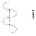
- FIG. 1illustrates the terms “period” and “frequency”.
- FIG. 2illustrates a display device
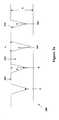
- FIG. 3 adepicts a luminance enhancement structure of the present invention.
- FIGS. 3 b and 3 cshow the three-dimensional view of the luminance enhancement structure.
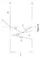
- FIGS. 4 a and 4 billustrate the dimensions of the luminance enhancement structure.
- FIG. 5depicts a display device with the luminance enhancement structure on its viewing side.
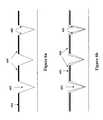
- FIGS. 6 a - 6 eillustrate the formation of a luminance enhancement structure coated with a metal layer.
- total internal reflectionrefers to an optical phenomenon that occurs when a ray of light strikes a medium boundary at an angle greater than the critical angle with respect to the normal axis to the surface. This can only occur where light travels from a medium with a higher refractive index to one with a lower refractive index.
- periodand “frequency” have the commonly known meanings.
- the time it takes to complete a cycle(360°, as indicated by arrows in FIG. 1 ) is a “period” and “frequency” is the inverse of the “period”. In other words, frequency is the number of cycles in a certain time frame.
- the term “Moiré pattern”is a pattern created by stacking one layer having a repetitive pattern on top of another layer also having a repetitive pattern.
- the two repeated patternsmay be different. For example, a Moiré pattern may become visible when a microcup layer is placed on top of a TFT (thin film transistor) layer.
- FIG. 2illustrates a display device ( 200 ).
- the devicecomprises an array of display cells ( 201 ) filled with a display fluid ( 202 ). Each of the display cells is surrounded by partition walls ( 203 ). The array of display cells is sandwiched between two electrode layers ( 204 and 205 ).
- the display cellsare filled with an electrophoretic fluid which comprises charged pigment particles dispersed in a solvent.
- the display fluidmay be a system comprising one or two types of particles.
- the charged pigment particlesare dispersed in a solvent of a contrasting color.
- the charged particleswill be drawn to one of the electrode layers ( 204 or 205 ), depending on the potential difference of the two electrode layers, thus causing the display panel to show either the color of the particles or the color of the solvent, on the viewing side.
- the particlesIn a system comprising particles carrying opposite charges and of two contrasting colors, the particles would move to one electrode layer or the other, based on the charge that they carry and the potential difference of the two electrode layers, causing the display panel to show the two contrasting colors, on the viewing side.
- the particlesmay be dispersed in a clear solvent.
- the display cellsmay also be filled with a liquid crystal composition.
- the present inventionis applicable to all types of reflective display devices.
- the two electrode layers ( 204 and 205 )are one common electrode (e.g., ITO) and one patterned segment electrode layer, respectively.
- the two electrode layers ( 204 and 205 )are one common electrode and an array of thin film transistor pixel electrodes, respectively.
- the two electrode layers ( 204 and 205 )are two line-patterned electrode layers.
- the electrode layersare usually formed on a substrate layer ( 206 ) [(such as polyethylene terephthalate (PET)).
- the thickness of the substrate layer ( 206 )is usually between about 5 ⁇ m to about 175 ⁇ m, more preferably between about 5 ⁇ m to about 50 ⁇ m.
- the substrate layermay also be a glass layer.
- the filled display cellsare sealed with a polymeric sealing layer.
- a display devicemay be viewed from the sealing layer side or the side opposite the sealing layer side, depending on the transparency of the materials used and the application.
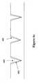
- FIG. 3 ais a cross-section view of a luminance enhancement structure ( 300 ) of the present invention.
- FIGS. 3 b and 3 care three-dimensional view of the luminance enhancement structure ( 300 ).
- the grooves ( 303 ) and the columns ( 302 )are in alternating order.
- the groovehas a triangular cross-section ( 301 ), an apex angle ⁇ and a top point A.
- the surface ( 304 ) of the groovesis optically flat and may optionally be coated with a metal layer.
- the terms “groove” or “grooves”refers to the groove or grooves the surface of which is either uncoated or coated. In one embodiment of the present invention, the surface of the groove or grooves is preferably uncoated.
- the columns ( 302 )have a top surface ( 305 ).
- the thickness of the luminance enhancement structuremay be in the range of about 10 ⁇ m to about 200 ⁇ m.
- the thickness of the luminance enhancement structureis expressed as the height (“h”) of the column ( 302 ) in FIGS. 3 a and 3 b.
- the luminance enhancement structureis formed from a material having a refractive index of about 1.4 to 1.7.
- the luminance enhancement structureis transparent.
- the columnshave wavy edges ( 306 ). Each column has two wavy edges, as shown in FIGS. 3 b and 3 c .
- the edgesshift in the X direction (i.e., horizontally) while the columns themselves extend in the Z direction. By having the edges shifting only in the X direction (i.e., horizontally), the surface ( 305 ) of the columns is on the same plane. This facilitates the lamination of the luminance enhancement structure to a display device.
- the X and Z directionsare indicated in FIG. 3 c .
- the Y direction(not indicated) is perpendicular to the plane of luminescent enhancement structure: i.e., is perpendicular to the plane of surface 305 .
- the widths (e.g., w 1 , w 2 , w 3 , etc.) of the top surface ( 305 ) of the columnare equal when cross-sectioned by parallel lines (e.g., L 1 , L 2 , L 3 , etc.).
- the widths (e.g., w 1 , w 1 ′, w 1 ′′, etc) of the top surface ( 305 ) of all columns ( 302 )are also equal when cross-sectioned by a same line.
- the variance of the horizontal shift of the edgesis generally small, preferably within 15% of the nominal or average period of the variance in the Z direction.
- the term “period”is the time needed to complete a cycle (as shown in FIG. 1 ).
- the variance of the shift patternmay change from one column to another column.
- the frequency of changes in the Z direction for each individual columnis usually high so that the changing patterns will not be detectable by human eyes.
- every columnhas a different horizontal shift pattern so that no column will have a shift pattern matching the shift pattern of another column within a certain range (e.g., within 10 or more columns). This design will help reduce the Moiré pattern when the luminance enhancement structure is laminated over a display device.
- FIGS. 4 a and 4 billustrate the dimensions of a groove of a luminance enhancement structure of the present invention.
- FIG. 4 ait is shown that the design aims to ensure an angle of incidence ⁇ 1 to be smaller than the critical angle C 1 (not shown) at the boundary between the top surface ( 407 ) of the luminance enhancement structure ( 400 ) and air.
- the critical angle C 1in this case, is about 42° based on the refractive index of the material for the luminance enhancement structure being 1.5 and the refractive index of air surrounding the top surface of the luminance enhancement structure being 1.
- the light ( 402 ) scattered from the surface ( 406 )(i.e., 305 in FIGS. 3 a - 3 c ) is reflected at the tilted surface ( 403 ) of the groove ( 401 ) and reaches the top surface ( 407 ) of the luminance enhancement structure ( 400 ).
- the apex angle ⁇ of the groove ( 401 )is preferably in the range of 5 to 50°, more preferably in the range of 15 to 30°.
- the angle ⁇is an angle at the intersection of the light ( 402 ) and the normal axis (marked Y) of the surface ( 406 ).
- An incoming light (not shown) from a light sourcetransmits through the luminance enhancement structure and strikes the display device and is then reflected with a scattering profile.
- the scattered light 402 in FIG. 4 ais an example of such a reflected light.
- FIG. 4 bdemonstrates that the tilted surface ( 403 ) of the groove ( 401 ) will reflect incoming light by total internal reflection.
- the designaims to ensure that the light striking the tilted surface ( 403 ) of the groove ( 401 ) will be reflected instead of transmitting through the space within the groove.
- the critical angle (not shown) at the boundary between the tilted surface ( 403 ) and the space within the groovemay be calculated based on the refractive index of the material for the luminance enhancement structure and the refractive index of what is filled in the space of the groove ( 401 ). If the groove is unfilled, the refractive index of air is about 1.
- the critical angle C 2would be about 42°.
- the angle of incidence ⁇ 2 of the light ( 408 ) coming from the surface ( 407 )is greater than 42°, the light striking the tilted surface ( 403 ) will be totally internal reflected towards the surface 406 which is desired in this case because, otherwise, the light would transmit through the space in the groove.
- a reflective tilted surfacemay be achieved by coating a metal layer over the surface of the groove.
- the surface of the groovesis uncoated.
- FIG. 5depicts a cross-section view of the luminance enhancement structure on the viewing side of the display device.
- the luminance enhancement structure of FIG. 3 ahas been turned 180°, with the top surface ( 305 ) of the columns ( 302 ) now in optical contact with the substrate layer ( 206 ) of the display device, which means that there is no air gap between the top surface 305 and the substrate layer 206 .
- Thismay be achieved by an optical adhesive material, such as the Norland® optical adhesive.
- the thickness of the substrate layer ( 206 ) between the luminance enhancement structure and the display deviceis preferably in the range of about 0 to about 25 ⁇ m, preferably in the range of about 0 to about 20 ⁇ m.
- the space within the grooves ( 303 )usually is filled with air. It is also possible for the space to be in a vacuum state. Alternatively, the space in the grooves ( 303 ) may be filled with a low refractive index material, lower than the refractive index of the material forming the luminance enhancement structure.
- the luminance enhancement structuremay be fabricated in many different ways.
- a Fast Tool Servo system with precision single point diamond turningis one of the methods which may be used to manufacture the luminance enhancement structure.
- the hard toolsmay be very small diamond tools mounted on CNC (computer numeric control) machines (e.g., turning, milling and ruling/shaping machines). These machines may have vibration devices attached to assist the tools to create the horizontal shifts with different levels of irregularity. Examples include STS (Slow Tool Servo), FTS (Fast Tool Servo) and other ultrasonic vibration apparatus.
- STSSmall Tool Servo
- FTSFast Tool Servo
- U.S. Pat. No. 6,581,286discloses one of the applications of the FTS for creating grooves on an optical film by using thread cutting.
- the toolis mounted onto the machine to create constant peak apex angle of cavities in relation to X-Y planes along the Z direction within a basic element.
- the non-regularity design of the present inventioncauses every column to redirect the light by a different factor, resulting in a different viewing angle distribution for every column, which are then combined to form a more uniform changing viewing angle for the luminance enhancement structure.
- the refraction index of the material for forming the luminance enhancement structureis preferably greater than about 1.4, more preferably between about 1.5 and about 1.7.
- the luminance enhancement structuremay be used as is or further coated with a metal layer.
- a metal layeris then deposited over the surface of the grooves.
- Suitable metals for this stepmay include, but are not limited to, aluminum, copper, zinc, tin, molybdenum, nickel, chromium, silver, gold, iron, indium, thallium, titanium, tantalum, tungsten, rhodium, palladium, platinum and cobalt.
- Aluminumis usually preferred.
- the metal materialmust be reflective, and it may be deposited on the surface of the grooves, using a variety of techniques such as sputtering, evaporation, roll transfer coating, electroless plating or the like.
- a strippable masking layermay be coated before metal deposition, over the surface on which the metal layer is not to be deposited. As shown in FIG. 6 a , a strippable masking layer ( 604 ) is coated onto the surface ( 605 ) between the openings of the grooves. The strippable masking layer is not coated on the surface ( 602 ) of the grooves ( 603 ).
- the coating of the strippable masking layermay be accomplished by a printing technique, such as flexographic printing, driographic printing, electrophotographic printing, lithographic printing, gravure printing, thermal printing, inkjet printing or screen printing.
- the coatingmay also be accomplished by a transfer-coating technique involving the use of a release layer.
- the strippable masking layerpreferably has a thickness in the range of about 0.01 to about 20 microns, more preferably about 1 to about 10 microns.
- the layeris preferably formed from a water-soluble or water-dispersible material.
- Organic materialsmay also be used.
- the strippable masking layermay be formed from a re-dispersible particulate material.
- the advantage of the re-dispersible particulate materialis that the coated layer may be easily removed without using a solubility enhancer.
- the term “re-dispersible particulate”is derived from the observation that the presence of particles in the material in a significant quantity will not decrease the stripping ability of a dried coating and, on the contrary, their presence actually enhances the stripping speed of the coated layer.
- the re-dispersible particulateconsists of particles that are surface treated to be hydrophilic through anionic, cationic or non-ionic functionalities. Their sizes are in microns, preferably in the range of about 0.1 to about 15 um and more preferably in the range of about 0.3 to about 8 um. Particles in these size ranges have been found to create proper surface roughness on a coated layer having a thickness of ⁇ 15 um.
- the re-dispersible particulatemay have a surface area in the range of about 50 to about 500 m 2 /g, preferably in the range of about 200 to about 400 m 2 /g.
- the interior of the re-dispersible particulatemay also be modified to have a pore volume in the range of about 0.3 to about 3.0 ml/g, preferably in the range of about 0.7 to about 2.0 ml/g.
- re-dispersible particulatesmay include, but are not limited to, micronized silica particles, such as those of the Sylojet series or Syloid series from Grace Davison, Columbia, Md., USA.
- Non-porous nano sized water re-dispersible colloid silica particlessuch as LUDOX AM can also be used together with the micron sized particles to enhance both the surface hardness and stripping rate of the coated layer.
- organic and inorganic particleswith sufficient hydrophilicity through surface treatment, may also be suitable.
- the surface modificationcan be achieved by inorganic and organic surface modification.
- the surface treatmentprovides the dispensability of the particles in water and the re-wettability in the coated layer.
- a metal layer ( 601 )is shown to be deposited over the entire surface, including the surface ( 602 ) of the grooves and the surface ( 605 ) between the grooves.
- Suitable metal materialsare those as described above.
- the metal materialmust be reflective and may be deposited by a variety of techniques previously described.
- FIG. 6 cshows the structure after removal of the strippable masking layer ( 604 ) with the metal layer 601 coated thereon.
- This stepmay be carried out with an aqueous or non-aqueous solvent such as water, MEK, acetone, ethanol or isopropanol or the like, depending on the material used for the strippable masking layer.
- the strippable masking layermay also be removed by mechanical means, such as brushing, using a spray nozzle or peeling it off with an adhesive layer. While removing the strippable masking layer ( 604 ), the metal layer ( 601 ) deposited on the strippable masking layer is also removed, leaving the metal layer ( 601 ) only on the surface ( 602 ) of the grooves.
- FIGS. 6 d and 6 edepict an alternative process for depositing the metal layer.
- a metal layer ( 601 )is deposited over the entire surface first, including both the surface ( 602 ) of the grooves and the surface ( 605 ) between the grooves.
- FIG. 6 eshows that the film of grooves deposited with a metal layer ( 601 ) is laminated with a film ( 606 ) coated with an adhesive layer ( 607 ).
- the metal layer ( 601 ) on top of the surface ( 605 )may be conveniently peeled off when the film of grooves is delaminated (separated) from the adhesive layer ( 607 ) coated film ( 606 ).
- the thickness of the adhesive layer ( 607 ) on the adhesive coated filmis preferably in the range of about 1 to about 50 um and more preferably in the range of about 2 to about 10 um.
- the luminance enhancement structurecomprising grooves (uncoated or coated with a metal layer) is then laminated over a layer of display cells as described above.
Landscapes
- Physics & Mathematics (AREA)
- General Physics & Mathematics (AREA)
- Optics & Photonics (AREA)
- Optical Elements Other Than Lenses (AREA)
Abstract
Description
- This application claims priority to U.S. Provisional Application No. 61/120,243, filed Dec. 5, 2008; the content of which is incorporated herein by reference in its entirety.
- The present invention is directed to a luminance enhancement structure for reflective display devices. The structure not only can enhance the brightness of a display device; but also can reduce the Moiré pattern effect.
- The lack of satisfactory brightness is often a concern for electrophoretic display devices. Total internal reflection would occur with electrophoretic display devices due to the fact that the display device usually has components of a high refractive index. Because of the components having a higher refractive index (e.g., about 1.5) than the air (which has a refractive index of about 1) surrounding the display panel, some of the scattering light from the display panel may reflect back to the display device by total internal reflection. This total internal reflection phenomenon could result in a loss of about 30-50% of the scattering light, thus causing reduction in brightness.
- A luminance enhancement structure can be used to enhance the brightness of an electrophoretic display. However, when a luminance enhancement structure is applied onto an electrophoretic display, the Moiré effect may occur which could significantly affect the quality of the images displayed. The Moiré effect may be avoided by designing different luminance enhancement structures for different display devices, depending on the size and shape of the display cells of the display device. In other words, depending on the size and shape of its display cells (or other equivalent repeated patterns, such as active matrix backplane), each display device has to have a customized luminance enhancement structure to avoid the Moiré effect. Such an approach obviously is not desirable because it could be costly.
- The present invention is directed to a luminance enhancement structure which not only can enhance the brightness of a display device, but also can reduce the Moiré effect, regardless of the size and shape of the display cells in the display device. Moreover, the luminance enhancement structure of the present invention has the additional advantage that the brightness of the display device may change depending on the viewing angle, in a more uniform manner.
- One aspect of the invention is directed to a luminance enhancement structure which comprises columns and grooves wherein said columns have wavy edges. In one embodiment, the grooves have a triangular cross-section. The surface of the grooves is optically flat and optionally coated with a metal layer. In one embodiment, the enhancement structure has a thickness in the range of about 10 μm to about 200 μm. In one embodiment, the enhancement structure is formed from a material having a refractive index of about 1.4 to 1.7. In one embodiment, the wavy edges shift in the X direction while the columns themselves extend in the Z direction. In one embodiment, the widths of the top surface of the columns are equal when cross-sectioned by parallel lines. In one embodiment, the grooves have the same apex angle. In one embodiment, the variance of the shift of the wavy edges is within 15% of the nominal or average period of the variance in the Z direction. In one embodiment, no column has a shift pattern of the wavy edges matching the shift pattern of another column within 10 or more columns.
- Another aspect of the invention is directed to a display device which comprises an array of microcups and a luminance enhancement structure on the viewing side of the display device wherein said luminance enhancement structure comprises columns and grooves and said columns have wavy edges. In one embodiment, the grooves have a triangular cross-section. In one embodiment, the surface of the grooves is optically flat and optionally coated with a metal layer. In one embodiment, the luminance enhancement structure has a thickness in the range of about 10 μm to about 200 μm. In one embodiment, the luminance enhancement structure is formed from a material having a refractive index of about 1.4 to 1.7. In one embodiment, the wavy edges shift in the X direction while the columns themselves extend in the Z direction. In one embodiment, the widths of the top surface of the columns are equal when cross-sectioned by parallel lines. In one embodiment, the grooves have the same apex angle. In one embodiment, the variance of the shift of the wavy edges is within 15% of the nominal or average period of the variance in the Z direction. In one embodiment, no column has a shift pattern of the wavy edges matching the shift pattern of another column within 10 or more columns. In one embodiment, the microcups are filled with an electrophoretic fluid. In one embodiment, the display device further comprises two electrode layers. One of the electrode layers comprises thin film transistor pixel electrodes or is a patterned segment electrode layer.
FIG. 1 illustrates the terms “period” and “frequency”.FIG. 2 illustrates a display device.FIG. 3 adepicts a luminance enhancement structure of the present invention.FIGS. 3 band3cshow the three-dimensional view of the luminance enhancement structure.FIGS. 4 aand4billustrate the dimensions of the luminance enhancement structure.FIG. 5 depicts a display device with the luminance enhancement structure on its viewing side.FIGS. 6 a-6eillustrate the formation of a luminance enhancement structure coated with a metal layer.- The technical term “total internal reflection” used in this application refers to an optical phenomenon that occurs when a ray of light strikes a medium boundary at an angle greater than the critical angle with respect to the normal axis to the surface. This can only occur where light travels from a medium with a higher refractive index to one with a lower refractive index.
- Generally speaking, when a ray of light crosses a boundary between materials with different refractive indices, the light will be partially refracted at the boundary surface, and partially reflected. However, if the angle of incidence is greater than the critical angle, the light will stop crossing the boundary and instead be totally reflected back.
- The critical angle is calculated based on the equation of Snell's law: C=sin−1(n2/n1) wherein n1 and n2 are the refractive indices of the two different media, with n1 being the higher refractive index and n2 being the lower refractive index.
- The terms “period” and “frequency” have the commonly known meanings. The time it takes to complete a cycle (360°, as indicated by arrows in
FIG. 1 ) is a “period” and “frequency” is the inverse of the “period”. In other words, frequency is the number of cycles in a certain time frame. - The term “Moiré pattern” is a pattern created by stacking one layer having a repetitive pattern on top of another layer also having a repetitive pattern. The two repeated patterns may be different. For example, a Moiré pattern may become visible when a microcup layer is placed on top of a TFT (thin film transistor) layer.
FIG. 2 illustrates a display device (200). The device comprises an array of display cells (201) filled with a display fluid (202). Each of the display cells is surrounded by partition walls (203). The array of display cells is sandwiched between two electrode layers (204 and205).- For an electrophoretic display panel, the display cells are filled with an electrophoretic fluid which comprises charged pigment particles dispersed in a solvent. The display fluid may be a system comprising one or two types of particles.
- In the system comprising only one type of particles, the charged pigment particles are dispersed in a solvent of a contrasting color. The charged particles will be drawn to one of the electrode layers (204 or205), depending on the potential difference of the two electrode layers, thus causing the display panel to show either the color of the particles or the color of the solvent, on the viewing side.
- In a system comprising particles carrying opposite charges and of two contrasting colors, the particles would move to one electrode layer or the other, based on the charge that they carry and the potential difference of the two electrode layers, causing the display panel to show the two contrasting colors, on the viewing side. In this case, the particles may be dispersed in a clear solvent.
- The display cells may also be filled with a liquid crystal composition. In addition, it is understood that the present invention is applicable to all types of reflective display devices.
- For a segment display device, the two electrode layers (204 and205) are one common electrode (e.g., ITO) and one patterned segment electrode layer, respectively. For an active matrix display device, the two electrode layers (204 and205) are one common electrode and an array of thin film transistor pixel electrodes, respectively. For a passive matrix display device, the two electrode layers (204 and205) are two line-patterned electrode layers.
- The electrode layers are usually formed on a substrate layer (206) [(such as polyethylene terephthalate (PET)). The thickness of the substrate layer (206) is usually between about 5 μm to about 175 μm, more preferably between about 5 μm to about 50 μm. The substrate layer may also be a glass layer.
- For a microcup-based display device disclosed in U.S. Pat. No. 6,930,818, the content of which is incorporated herein by reference in its entirety, the filled display cells are sealed with a polymeric sealing layer. Such a display device may be viewed from the sealing layer side or the side opposite the sealing layer side, depending on the transparency of the materials used and the application.
FIG. 3 ais a cross-section view of a luminance enhancement structure (300) of the present invention.FIGS. 3 band3care three-dimensional view of the luminance enhancement structure (300). There are multiple columns (302) and grooves (303) across the structure. The grooves (303) and the columns (302) are in alternating order.- The groove has a triangular cross-section (301), an apex angle α and a top point A. The surface (304) of the grooves is optically flat and may optionally be coated with a metal layer. In the context of this application, the terms “groove” or “grooves” refers to the groove or grooves the surface of which is either uncoated or coated. In one embodiment of the present invention, the surface of the groove or grooves is preferably uncoated. The columns (302) have a top surface (305).
- The thickness of the luminance enhancement structure may be in the range of about 10 μm to about 200 μm. The thickness of the luminance enhancement structure is expressed as the height (“h”) of the column (302) in
FIGS. 3 aand3b. - The luminance enhancement structure is formed from a material having a refractive index of about 1.4 to 1.7. The luminance enhancement structure is transparent.
- The columns have wavy edges (306). Each column has two wavy edges, as shown in
FIGS. 3 band3c. The edges shift in the X direction (i.e., horizontally) while the columns themselves extend in the Z direction. By having the edges shifting only in the X direction (i.e., horizontally), the surface (305) of the columns is on the same plane. This facilitates the lamination of the luminance enhancement structure to a display device. The X and Z directions are indicated inFIG. 3 c. The Y direction (not indicated) is perpendicular to the plane of luminescent enhancement structure: i.e., is perpendicular to the plane ofsurface 305. - In a single column, the widths (e.g., w1, w2, w3, etc.) of the top surface (305) of the column are equal when cross-sectioned by parallel lines (e.g., L1, L2, L3, etc.). In addition, the widths (e.g., w1, w1′, w1″, etc) of the top surface (305) of all columns (302) are also equal when cross-sectioned by a same line.
- The horizontal shift of the edges, however, will cause the base width (w) of the grooves (303) to vary. As a result, the depth (d) of the grooves will also vary. The apex angles of all the grooves are equal in the same luminance enhancement structure.
- The variance of the horizontal shift of the edges is generally small, preferably within 15% of the nominal or average period of the variance in the Z direction. The term “period” is the time needed to complete a cycle (as shown in
FIG. 1 ). - The variance of the shift pattern may change from one column to another column. The frequency of changes in the Z direction for each individual column is usually high so that the changing patterns will not be detectable by human eyes.
- It is preferred that every column has a different horizontal shift pattern so that no column will have a shift pattern matching the shift pattern of another column within a certain range (e.g., within 10 or more columns). This design will help reduce the Moiré pattern when the luminance enhancement structure is laminated over a display device.
FIGS. 4 aand4billustrate the dimensions of a groove of a luminance enhancement structure of the present invention.- In
FIG. 4 a, it is shown that the design aims to ensure an angle of incidence θ1to be smaller than the critical angle C1(not shown) at the boundary between the top surface (407) of the luminance enhancement structure (400) and air. - The critical angle C1, in this case, is about 42° based on the refractive index of the material for the luminance enhancement structure being 1.5 and the refractive index of air surrounding the top surface of the luminance enhancement structure being 1.
- As shown in
FIG. 4 a, the light (402) scattered from the surface (406) (i.e.,305 inFIGS. 3 a-3c) is reflected at the tilted surface (403) of the groove (401) and reaches the top surface (407) of the luminance enhancement structure (400). In order for the angle of incidence (θ1) at the top surface of the luminance enhancement structure to be smaller than 42°, the apex angle α of the groove (401) is preferably in the range of 5 to 50°, more preferably in the range of 15 to 30°. As a result, the angle of incidence θ1will be smaller than the angle γ, which reduces the chance of total internal reflection at the top surface and increases the overall optical efficiency. The angle γ is an angle at the intersection of the light (402) and the normal axis (marked Y) of the surface (406). - An incoming light (not shown) from a light source transmits through the luminance enhancement structure and strikes the display device and is then reflected with a scattering profile. The
scattered light 402 inFIG. 4 ais an example of such a reflected light. FIG. 4 bdemonstrates that the tilted surface (403) of the groove (401) will reflect incoming light by total internal reflection. The design aims to ensure that the light striking the tilted surface (403) of the groove (401) will be reflected instead of transmitting through the space within the groove. The critical angle (not shown) at the boundary between the tilted surface (403) and the space within the groove may be calculated based on the refractive index of the material for the luminance enhancement structure and the refractive index of what is filled in the space of the groove (401). If the groove is unfilled, the refractive index of air is about 1. With the refractive index of the material for the luminance enhancement structure being about 1.5, the critical angle C2would be about 42°. When the angle of incidence θ2of the light (408) coming from the surface (407) is greater than 42°, the light striking the tilted surface (403) will be totally internal reflected towards thesurface 406 which is desired in this case because, otherwise, the light would transmit through the space in the groove.- A reflective tilted surface may be achieved by coating a metal layer over the surface of the groove. However, in one embodiment of the present invention, the surface of the grooves is uncoated.
FIG. 5 depicts a cross-section view of the luminance enhancement structure on the viewing side of the display device. As shown, the luminance enhancement structure ofFIG. 3 ahas been turned 180°, with the top surface (305) of the columns (302) now in optical contact with the substrate layer (206) of the display device, which means that there is no air gap between thetop surface 305 and thesubstrate layer 206. This may be achieved by an optical adhesive material, such as the Norland® optical adhesive.- The thickness of the substrate layer (206) between the luminance enhancement structure and the display device is preferably in the range of about 0 to about 25 μm, preferably in the range of about 0 to about 20 μm.
- The space within the grooves (303) usually is filled with air. It is also possible for the space to be in a vacuum state. Alternatively, the space in the grooves (303) may be filled with a low refractive index material, lower than the refractive index of the material forming the luminance enhancement structure.
- The luminance enhancement structure may be fabricated in many different ways.
- A Fast Tool Servo system with precision single point diamond turning is one of the methods which may be used to manufacture the luminance enhancement structure. The hard tools may be very small diamond tools mounted on CNC (computer numeric control) machines (e.g., turning, milling and ruling/shaping machines). These machines may have vibration devices attached to assist the tools to create the horizontal shifts with different levels of irregularity. Examples include STS (Slow Tool Servo), FTS (Fast Tool Servo) and other ultrasonic vibration apparatus. U.S. Pat. No. 6,581,286 discloses one of the applications of the FTS for creating grooves on an optical film by using thread cutting. The tool is mounted onto the machine to create constant peak apex angle of cavities in relation to X-Y planes along the Z direction within a basic element. By using a tool to form surfaces in a mold in relation to increasing degrees of freedom, three-dimensionally varying irregular prism blocks of the structured surfaces of the optical substrates can be obtained.
- The non-regularity design of the present invention causes every column to redirect the light by a different factor, resulting in a different viewing angle distribution for every column, which are then combined to form a more uniform changing viewing angle for the luminance enhancement structure.
- The refraction index of the material for forming the luminance enhancement structure is preferably greater than about 1.4, more preferably between about 1.5 and about 1.7.
- The luminance enhancement structure may be used as is or further coated with a metal layer. In the latter case, a metal layer is then deposited over the surface of the grooves. Suitable metals for this step may include, but are not limited to, aluminum, copper, zinc, tin, molybdenum, nickel, chromium, silver, gold, iron, indium, thallium, titanium, tantalum, tungsten, rhodium, palladium, platinum and cobalt. Aluminum is usually preferred. The metal material must be reflective, and it may be deposited on the surface of the grooves, using a variety of techniques such as sputtering, evaporation, roll transfer coating, electroless plating or the like.
- In order to facilitate formation of the metal layer only on the intended surface of the grooves, a strippable masking layer may be coated before metal deposition, over the surface on which the metal layer is not to be deposited. As shown in
FIG. 6 a, a strippable masking layer (604) is coated onto the surface (605) between the openings of the grooves. The strippable masking layer is not coated on the surface (602) of the grooves (603). - The coating of the strippable masking layer may be accomplished by a printing technique, such as flexographic printing, driographic printing, electrophotographic printing, lithographic printing, gravure printing, thermal printing, inkjet printing or screen printing. The coating may also be accomplished by a transfer-coating technique involving the use of a release layer. The strippable masking layer preferably has a thickness in the range of about 0.01 to about 20 microns, more preferably about 1 to about 10 microns.
- For ease of stripping, the layer is preferably formed from a water-soluble or water-dispersible material. Organic materials may also be used. For example, the strippable masking layer may be formed from a re-dispersible particulate material. The advantage of the re-dispersible particulate material is that the coated layer may be easily removed without using a solubility enhancer. The term “re-dispersible particulate” is derived from the observation that the presence of particles in the material in a significant quantity will not decrease the stripping ability of a dried coating and, on the contrary, their presence actually enhances the stripping speed of the coated layer.
- The re-dispersible particulate consists of particles that are surface treated to be hydrophilic through anionic, cationic or non-ionic functionalities. Their sizes are in microns, preferably in the range of about 0.1 to about 15 um and more preferably in the range of about 0.3 to about 8 um. Particles in these size ranges have been found to create proper surface roughness on a coated layer having a thickness of <15 um. The re-dispersible particulate may have a surface area in the range of about 50 to about 500 m2/g, preferably in the range of about 200 to about 400 m2/g. The interior of the re-dispersible particulate may also be modified to have a pore volume in the range of about 0.3 to about 3.0 ml/g, preferably in the range of about 0.7 to about 2.0 ml/g.
- Commercially available re-dispersible particulates may include, but are not limited to, micronized silica particles, such as those of the Sylojet series or Syloid series from Grace Davison, Columbia, Md., USA.
- Non-porous nano sized water re-dispersible colloid silica particles, such as LUDOX AM can also be used together with the micron sized particles to enhance both the surface hardness and stripping rate of the coated layer.
- Other organic and inorganic particles, with sufficient hydrophilicity through surface treatment, may also be suitable. The surface modification can be achieved by inorganic and organic surface modification. The surface treatment provides the dispensability of the particles in water and the re-wettability in the coated layer.
- In
FIG. 6 b, a metal layer (601) is shown to be deposited over the entire surface, including the surface (602) of the grooves and the surface (605) between the grooves. Suitable metal materials are those as described above. The metal material must be reflective and may be deposited by a variety of techniques previously described. FIG. 6 cshows the structure after removal of the strippable masking layer (604) with themetal layer 601 coated thereon. This step may be carried out with an aqueous or non-aqueous solvent such as water, MEK, acetone, ethanol or isopropanol or the like, depending on the material used for the strippable masking layer. The strippable masking layer may also be removed by mechanical means, such as brushing, using a spray nozzle or peeling it off with an adhesive layer. While removing the strippable masking layer (604), the metal layer (601) deposited on the strippable masking layer is also removed, leaving the metal layer (601) only on the surface (602) of the grooves.FIGS. 6 dand6edepict an alternative process for depositing the metal layer. InFIG. 6 d, a metal layer (601) is deposited over the entire surface first, including both the surface (602) of the grooves and the surface (605) between the grooves.FIG. 6 eshows that the film of grooves deposited with a metal layer (601) is laminated with a film (606) coated with an adhesive layer (607). The metal layer (601) on top of the surface (605) may be conveniently peeled off when the film of grooves is delaminated (separated) from the adhesive layer (607) coated film (606). The thickness of the adhesive layer (607) on the adhesive coated film is preferably in the range of about 1 to about 50 um and more preferably in the range of about 2 to about 10 um.- The luminance enhancement structure comprising grooves (uncoated or coated with a metal layer) is then laminated over a layer of display cells as described above.
- While the present invention has been described with reference to the specific embodiments thereof, it should be understood by those skilled in the art that various changes may be made and equivalents may be substituted without departing from the true spirit and scope of the invention. In addition, many modifications may be made to adapt a particular situation, materials, compositions, processes, process step or steps, to the objective, spirit and scope of the present invention. All such modifications are intended to be within the scope of the claims appended hereto.
Claims (24)
Priority Applications (1)
| Application Number | Priority Date | Filing Date | Title |
|---|---|---|---|
| US12/628,014US8441414B2 (en) | 2008-12-05 | 2009-11-30 | Luminance enhancement structure with Moiré reducing design |
Applications Claiming Priority (2)
| Application Number | Priority Date | Filing Date | Title |
|---|---|---|---|
| US12024308P | 2008-12-05 | 2008-12-05 | |
| US12/628,014US8441414B2 (en) | 2008-12-05 | 2009-11-30 | Luminance enhancement structure with Moiré reducing design |
Publications (2)
| Publication Number | Publication Date |
|---|---|
| US20100141573A1true US20100141573A1 (en) | 2010-06-10 |
| US8441414B2 US8441414B2 (en) | 2013-05-14 |
Family
ID=42230509
Family Applications (1)
| Application Number | Title | Priority Date | Filing Date |
|---|---|---|---|
| US12/628,014Active2032-01-10US8441414B2 (en) | 2008-12-05 | 2009-11-30 | Luminance enhancement structure with Moiré reducing design |
Country Status (1)
| Country | Link |
|---|---|
| US (1) | US8441414B2 (en) |
Cited By (12)
| Publication number | Priority date | Publication date | Assignee | Title |
|---|---|---|---|---|
| US20100182351A1 (en)* | 2009-01-22 | 2010-07-22 | Craig Lin | Luminance enhancement structure with varying pitches |
| US20100225999A1 (en)* | 2009-03-09 | 2010-09-09 | Craig Lin | Luminance enhancement structure for reflective display devices |
| US20100271407A1 (en)* | 2009-04-22 | 2010-10-28 | Andrew Ho | Reflective display devices with luminance enhancement film |
| US20110043543A1 (en)* | 2009-08-18 | 2011-02-24 | Hui Chen | Color tuning for electrophoretic display |
| US20110043894A1 (en)* | 2007-11-30 | 2011-02-24 | Sprague Robert A | Display devices having micro-reflectors and color filters |
| US20110057927A1 (en)* | 2008-03-11 | 2011-03-10 | Craig Lin | Luminance enhancement structure for reflective display devices |
| US8237892B1 (en) | 2007-11-30 | 2012-08-07 | Sipix Imaging, Inc. | Display device with a brightness enhancement structure |
| US8395836B2 (en) | 2008-03-11 | 2013-03-12 | Sipix Imaging, Inc. | Luminance enhancement structure for reflective display devices |
| US8456589B1 (en) | 2009-07-27 | 2013-06-04 | Sipix Imaging, Inc. | Display device assembly |
| US8797633B1 (en) | 2009-07-23 | 2014-08-05 | Sipix Imaging, Inc. | Display device assembly and manufacture thereof |
| CN111323982A (en)* | 2020-03-09 | 2020-06-23 | 合肥京东方光电科技有限公司 | Peep-proof film, backlight source and display device |
| US20210191223A1 (en)* | 2018-09-12 | 2021-06-24 | Hewlett-Packard Development Company, L.P. | Privacy films for electronic displays |
Families Citing this family (23)
| Publication number | Priority date | Publication date | Assignee | Title |
|---|---|---|---|---|
| CN107167982A (en)* | 2012-02-14 | 2017-09-15 | 伊英克加利福尼亚有限责任公司 | Micro-cup for electrophoretic display device (EPD) is designed |
| US9383623B2 (en) | 2013-05-17 | 2016-07-05 | E Ink California, Llc | Color display device |
| US10317767B2 (en) | 2014-02-07 | 2019-06-11 | E Ink Corporation | Electro-optic display backplane structure with drive components and pixel electrodes on opposed surfaces |
| TWI518435B (en) | 2014-12-10 | 2016-01-21 | 元太科技工業股份有限公司 | Reflective display device |
| JP6876727B2 (en) | 2016-06-10 | 2021-05-26 | イー インク コーポレイション | Electro-optic display device |
| US10324577B2 (en) | 2017-02-28 | 2019-06-18 | E Ink Corporation | Writeable electrophoretic displays including sensing circuits and styli configured to interact with sensing circuits |
| EP3602193A4 (en) | 2017-03-28 | 2021-01-06 | E Ink Corporation | POROUS BACK PANEL FOR ELECTRO-OPTICAL DISPLAY |
| CN112860018B (en) | 2017-05-19 | 2024-12-27 | 伊英克公司 | Foldable electro-optical display with digitization and touch sensing |
| KR20190133292A (en) | 2017-05-30 | 2019-12-02 | 이 잉크 코포레이션 | Electro-optic displays |
| US11404013B2 (en) | 2017-05-30 | 2022-08-02 | E Ink Corporation | Electro-optic displays with resistors for discharging remnant charges |
| US10882042B2 (en) | 2017-10-18 | 2021-01-05 | E Ink Corporation | Digital microfluidic devices including dual substrates with thin-film transistors and capacitive sensing |
| US10824042B1 (en) | 2017-10-27 | 2020-11-03 | E Ink Corporation | Electro-optic display and composite materials having low thermal sensitivity for use therein |
| US11175561B1 (en) | 2018-04-12 | 2021-11-16 | E Ink Corporation | Electrophoretic display media with network electrodes and methods of making and using the same |
| US11353759B2 (en) | 2018-09-17 | 2022-06-07 | Nuclera Nucleics Ltd. | Backplanes with hexagonal and triangular electrodes |
| TWI763526B (en) | 2018-10-15 | 2022-05-01 | 美商電子墨水股份有限公司 | Method for dispensing an aqueous chemical species to a surface |
| US11145262B2 (en) | 2018-11-09 | 2021-10-12 | E Ink Corporation | Electro-optic displays |
| CN113228151B (en) | 2018-12-30 | 2024-03-29 | 伊英克公司 | electro-optical display |
| JP7506769B2 (en) | 2020-06-03 | 2024-06-26 | イー インク コーポレイション | Foldable electrophoretic display module including a non-conductive support plate - Patents.com |
| EP4388370A4 (en) | 2021-08-18 | 2025-07-02 | E Ink Corp | METHOD FOR CONTROLLING ELECTRO-OPTICAL DISPLAYS |
| WO2023164099A1 (en) | 2022-02-28 | 2023-08-31 | E Ink Corporation | Parking space management system |
| US11830449B2 (en) | 2022-03-01 | 2023-11-28 | E Ink Corporation | Electro-optic displays |
| US20250224645A1 (en) | 2024-01-05 | 2025-07-10 | E Ink Corporation | Electrophoretic medium comprising particles having a pigment core and a polymeric shell |
| US20250224646A1 (en) | 2024-01-08 | 2025-07-10 | E Ink Corporation | Adhesive Layer Comprising Conductive Filler Particles and a Polymeric Dispersant |
Citations (57)
| Publication number | Priority date | Publication date | Assignee | Title |
|---|---|---|---|---|
| US4083626A (en)* | 1975-04-04 | 1978-04-11 | Fuji Photo Film Co., Ltd. | Rear projection screens |
| US5151801A (en)* | 1989-11-30 | 1992-09-29 | Pioneer Electronic Corporation | Liquid crystal display apparatus providing improved illumination via trucated prisms |
| US6144430A (en)* | 1997-11-13 | 2000-11-07 | Industrial Technology Research Institute | Reflective-type liquid crystal display with single polarizer and an inner metallic reflector |
| US6166787A (en)* | 1998-03-17 | 2000-12-26 | Motorola, Inc. | Optical display device having prismatic film for enhanced viewing |
| US20010006409A1 (en)* | 1999-12-31 | 2001-07-05 | Lee Seung Chul | Liquid crystal display device with electrodes on barrier ribs and fabricating method thereof |
| US6277263B1 (en)* | 1998-03-20 | 2001-08-21 | Semitool, Inc. | Apparatus and method for electrolytically depositing copper on a semiconductor workpiece |
| US20010026347A1 (en)* | 2000-01-14 | 2001-10-04 | Fujitsu Ltd. | Liquid crystal display device and method of manufacturing the same |
| US20010026445A1 (en)* | 1999-06-11 | 2001-10-04 | David Naghi | Apparatus for illuminating a portable electronic or computing device |
| US6327013B1 (en)* | 1998-05-29 | 2001-12-04 | Sharp Kabushiki Kaisha | Liquid crystal device in which an electric field within the picture element varies in intensity |
| US20020033927A1 (en)* | 2000-08-14 | 2002-03-21 | Joong-Hyun Mun | Liquid crystal display and a method for fabricating the same |
| US20020057413A1 (en)* | 2000-09-25 | 2002-05-16 | Yukihiro Sumida | Method for fabricating a laminate film, laminate film, and method for fabricating a display device |
| US6556261B1 (en)* | 1999-02-15 | 2003-04-29 | Rainbow Displays, Inc. | Method for assembling a tiled, flat-panel microdisplay array having reflective microdisplay tiles and attaching thermally-conductive substrate |
| US6565729B2 (en)* | 1998-03-20 | 2003-05-20 | Semitool, Inc. | Method for electrochemically depositing metal on a semiconductor workpiece |
| US6581286B2 (en)* | 2000-04-05 | 2003-06-24 | 3M Innovative Properties Company | Method of making tool to produce optical film |
| US20030165016A1 (en)* | 2002-03-04 | 2003-09-04 | Whitehead Lorne A. | Wide viewing angle reflective display |
| US20030234900A1 (en)* | 2002-06-12 | 2003-12-25 | Yong-Ii Kim | Prism sheet and liquid crystal display having the same |
| US6753064B1 (en)* | 1997-10-24 | 2004-06-22 | Nippon Sheet Glass Co., Ltd. | Multi-layered coated substrate and method of production thereof |
| US6806995B2 (en)* | 2001-10-29 | 2004-10-19 | Sipix Imaging, Inc. | Electrophoretic display with holding electrodes |
| US20050041311A1 (en)* | 2003-08-18 | 2005-02-24 | Eastman Kodak Company | Brightness enhancement article |
| US20050141844A1 (en)* | 2003-12-31 | 2005-06-30 | General Electric Company | Faceted optical substrate and method of fabricating a faceted optical substrate and a backlight display comprising the faceted optical substrate |
| US20050140846A1 (en)* | 2002-10-17 | 2005-06-30 | Lubart Neil D. | Light control devices and methods of making same |
| US6930818B1 (en)* | 2000-03-03 | 2005-08-16 | Sipix Imaging, Inc. | Electrophoretic display and novel process for its manufacture |
| US6940569B2 (en)* | 2001-11-27 | 2005-09-06 | Sony Corporation | Information processing apparatus |
| US20060034099A1 (en)* | 2004-08-13 | 2006-02-16 | Innolux Display Corp. | Light guide plate with V-shaped grooves and backlight module incorporating the same |
| US20060055627A1 (en)* | 2004-09-13 | 2006-03-16 | Wilson Randall H | Randomized patterns of individual optical elements |
| US20060103779A1 (en)* | 2004-11-18 | 2006-05-18 | Hiroyuki Amemiya | View angle controlling sheet and liquid crystal display apparatus using the same |
| US7061569B2 (en)* | 2002-07-26 | 2006-06-13 | Samsung Electronics Co., Ltd. | Upper substrate, liquid crystal display apparatus having the same and method of fabricating the same |
| US7088404B2 (en)* | 2002-12-12 | 2006-08-08 | Seiko Epson Corporation | Substrate for electro-optical device having particular concave portions and convex portions and flat section on the surface of a base layer |
| US20060291247A1 (en)* | 2005-06-08 | 2006-12-28 | Au Optronics Corp. | Light guide plate having curved grooves |
| US7160017B2 (en)* | 2004-06-03 | 2007-01-09 | Eastman Kodak Company | Brightness enhancement film using a linear arrangement of light concentrators |
| US7184188B2 (en)* | 2005-02-07 | 2007-02-27 | Seiko Epson Corporation | Spatial light modulator and image display device |
| US20070152592A1 (en)* | 2005-12-30 | 2007-07-05 | Hyun Kim | Plasma display panel |
| US7248394B2 (en)* | 2005-03-15 | 2007-07-24 | Industrial Technology Research Institute | Transflective electrophoretic display and manufacturing method thereof |
| US20070200975A1 (en)* | 2006-02-14 | 2007-08-30 | Seiko Epson Corporation | Electro-optic device, method for manufacturing electro-optic device, projector, and electronic apparatus |
| US7286197B2 (en)* | 1999-11-05 | 2007-10-23 | Lg. Philips Lcd Co., Ltd. | Liquid crystal display having high brightness and enhanced viewing angle |
| US20070253072A1 (en)* | 2000-08-18 | 2007-11-01 | Mullen Patrick W | Differentially-cured materials and process for forming same |
| US7294866B2 (en)* | 2004-03-01 | 2007-11-13 | Epistar Corporation | Flip-chip light-emitting device with micro-reflector |
| US20080012034A1 (en)* | 2006-07-17 | 2008-01-17 | 3M Innovative Properties Company | Led package with converging extractor |
| US7339716B2 (en)* | 2004-10-22 | 2008-03-04 | Industrial Technology Research Institute | Transflective electrophoretic display device |
| US7342556B2 (en)* | 2002-11-28 | 2008-03-11 | Matsushita Electric Industrial Co., Ltd. | Display device and method of manufacturing same |
| US7397619B2 (en)* | 2003-07-31 | 2008-07-08 | Doosan Corporation | Prism sheet having concave pentagonal |
| US7408696B2 (en)* | 2000-03-03 | 2008-08-05 | Sipix Imaging, Inc. | Three-dimensional electrophoretic displays |
| US7463317B2 (en)* | 2001-07-27 | 2008-12-09 | Seiko Epson Corporation | Electro-optical device, color filter substrate with relective and transmission regions and electronic apparatus |
| US20090097273A1 (en)* | 2007-10-12 | 2009-04-16 | Industrial Technology Research Institute | Light guide plate and light-emitting apparatus |
| US7543973B2 (en)* | 2006-04-17 | 2009-06-09 | Citizen Electronics Co., Ltd. | Light guide plate, method of manufacturing light guide plate and backlight with the light guide plate |
| US7564519B2 (en)* | 2001-09-27 | 2009-07-21 | Seiko Epson Corporation | Electrooptical device substrate, electrooptical device, methods for fabricating electrooptical device substrate and electrooptical device, electronic apparatus, and method for tuning color of color filter |
| US7576914B2 (en)* | 2003-11-28 | 2009-08-18 | Dai Nippon Printing Co., Ltd. | Light-diffusing sheet |
| US20090231245A1 (en)* | 2008-03-11 | 2009-09-17 | Craig Lin | Luminance enhancement structure for reflective display devices |
| US7638808B2 (en)* | 2004-03-18 | 2009-12-29 | Phoseon Technology, Inc. | Micro-reflectors on a substrate for high-density LED array |
| US7667785B2 (en)* | 2004-06-17 | 2010-02-23 | Koninklijke Philips Electronics N.V. | Optical separating filter |
| US20100177396A1 (en)* | 2009-01-13 | 2010-07-15 | Craig Lin | Asymmetrical luminance enhancement structure for reflective display devices |
| US20100182351A1 (en)* | 2009-01-22 | 2010-07-22 | Craig Lin | Luminance enhancement structure with varying pitches |
| US20100225999A1 (en)* | 2009-03-09 | 2010-09-09 | Craig Lin | Luminance enhancement structure for reflective display devices |
| US20100271407A1 (en)* | 2009-04-22 | 2010-10-28 | Andrew Ho | Reflective display devices with luminance enhancement film |
| US7830592B1 (en)* | 2007-11-30 | 2010-11-09 | Sipix Imaging, Inc. | Display devices having micro-reflectors |
| US20110057927A1 (en)* | 2008-03-11 | 2011-03-10 | Craig Lin | Luminance enhancement structure for reflective display devices |
| US8237892B1 (en)* | 2007-11-30 | 2012-08-07 | Sipix Imaging, Inc. | Display device with a brightness enhancement structure |
Family Cites Families (4)
| Publication number | Priority date | Publication date | Assignee | Title |
|---|---|---|---|---|
| JP3641780B2 (en) | 2000-03-22 | 2005-04-27 | ナノックス株式会社 | Liquid crystal display |
| JP4530167B2 (en) | 2005-09-22 | 2010-08-25 | セイコーエプソン株式会社 | Electrophoresis device, electronic apparatus, and method for driving electrophoresis device |
| KR101257136B1 (en) | 2006-01-12 | 2013-04-23 | 쓰리엠 이노베이티브 프로퍼티즈 컴파니 | Light-collimating film |
| US7952792B2 (en) | 2007-04-06 | 2011-05-31 | Koninklijke Philips Electronics N.V. | Reflective display and method for manufacturing such a display |
- 2009
- 2009-11-30USUS12/628,014patent/US8441414B2/enactiveActive
Patent Citations (65)
| Publication number | Priority date | Publication date | Assignee | Title |
|---|---|---|---|---|
| US4083626A (en)* | 1975-04-04 | 1978-04-11 | Fuji Photo Film Co., Ltd. | Rear projection screens |
| US5151801A (en)* | 1989-11-30 | 1992-09-29 | Pioneer Electronic Corporation | Liquid crystal display apparatus providing improved illumination via trucated prisms |
| US6753064B1 (en)* | 1997-10-24 | 2004-06-22 | Nippon Sheet Glass Co., Ltd. | Multi-layered coated substrate and method of production thereof |
| US6144430A (en)* | 1997-11-13 | 2000-11-07 | Industrial Technology Research Institute | Reflective-type liquid crystal display with single polarizer and an inner metallic reflector |
| US6166787A (en)* | 1998-03-17 | 2000-12-26 | Motorola, Inc. | Optical display device having prismatic film for enhanced viewing |
| US6565729B2 (en)* | 1998-03-20 | 2003-05-20 | Semitool, Inc. | Method for electrochemically depositing metal on a semiconductor workpiece |
| US7332066B2 (en)* | 1998-03-20 | 2008-02-19 | Semitool, Inc. | Apparatus and method for electrochemically depositing metal on a semiconductor workpiece |
| US6277263B1 (en)* | 1998-03-20 | 2001-08-21 | Semitool, Inc. | Apparatus and method for electrolytically depositing copper on a semiconductor workpiece |
| US6327013B1 (en)* | 1998-05-29 | 2001-12-04 | Sharp Kabushiki Kaisha | Liquid crystal device in which an electric field within the picture element varies in intensity |
| US6556261B1 (en)* | 1999-02-15 | 2003-04-29 | Rainbow Displays, Inc. | Method for assembling a tiled, flat-panel microdisplay array having reflective microdisplay tiles and attaching thermally-conductive substrate |
| US20010026445A1 (en)* | 1999-06-11 | 2001-10-04 | David Naghi | Apparatus for illuminating a portable electronic or computing device |
| US7286197B2 (en)* | 1999-11-05 | 2007-10-23 | Lg. Philips Lcd Co., Ltd. | Liquid crystal display having high brightness and enhanced viewing angle |
| US20010006409A1 (en)* | 1999-12-31 | 2001-07-05 | Lee Seung Chul | Liquid crystal display device with electrodes on barrier ribs and fabricating method thereof |
| US20010026347A1 (en)* | 2000-01-14 | 2001-10-04 | Fujitsu Ltd. | Liquid crystal display device and method of manufacturing the same |
| US7408696B2 (en)* | 2000-03-03 | 2008-08-05 | Sipix Imaging, Inc. | Three-dimensional electrophoretic displays |
| US6930818B1 (en)* | 2000-03-03 | 2005-08-16 | Sipix Imaging, Inc. | Electrophoretic display and novel process for its manufacture |
| US6581286B2 (en)* | 2000-04-05 | 2003-06-24 | 3M Innovative Properties Company | Method of making tool to produce optical film |
| US20020033927A1 (en)* | 2000-08-14 | 2002-03-21 | Joong-Hyun Mun | Liquid crystal display and a method for fabricating the same |
| US20070253072A1 (en)* | 2000-08-18 | 2007-11-01 | Mullen Patrick W | Differentially-cured materials and process for forming same |
| US20050003108A1 (en)* | 2000-09-25 | 2005-01-06 | Sharp Kabushiki Kaisha | Method for fabricating a laminate film, laminate film, and method for fabricating a display device |
| US20020057413A1 (en)* | 2000-09-25 | 2002-05-16 | Yukihiro Sumida | Method for fabricating a laminate film, laminate film, and method for fabricating a display device |
| US7244476B2 (en)* | 2000-09-25 | 2007-07-17 | Sharp Kabushiki Kaisha | Display device including adhesive film with transparent support |
| US6784962B2 (en)* | 2000-09-25 | 2004-08-31 | Sharp Kabushiki Kaisha | Method for fabricating a laminate film and method for fabricating a display device |
| US7612846B2 (en)* | 2001-07-27 | 2009-11-03 | Seiko Epson Corporation | Electro-optical device, color filter substrate and electronic apparatus |
| US7463317B2 (en)* | 2001-07-27 | 2008-12-09 | Seiko Epson Corporation | Electro-optical device, color filter substrate with relective and transmission regions and electronic apparatus |
| US7564519B2 (en)* | 2001-09-27 | 2009-07-21 | Seiko Epson Corporation | Electrooptical device substrate, electrooptical device, methods for fabricating electrooptical device substrate and electrooptical device, electronic apparatus, and method for tuning color of color filter |
| US6806995B2 (en)* | 2001-10-29 | 2004-10-19 | Sipix Imaging, Inc. | Electrophoretic display with holding electrodes |
| US6940569B2 (en)* | 2001-11-27 | 2005-09-06 | Sony Corporation | Information processing apparatus |
| US20030165016A1 (en)* | 2002-03-04 | 2003-09-04 | Whitehead Lorne A. | Wide viewing angle reflective display |
| US20030234900A1 (en)* | 2002-06-12 | 2003-12-25 | Yong-Ii Kim | Prism sheet and liquid crystal display having the same |
| US7061569B2 (en)* | 2002-07-26 | 2006-06-13 | Samsung Electronics Co., Ltd. | Upper substrate, liquid crystal display apparatus having the same and method of fabricating the same |
| US20050140846A1 (en)* | 2002-10-17 | 2005-06-30 | Lubart Neil D. | Light control devices and methods of making same |
| US7342556B2 (en)* | 2002-11-28 | 2008-03-11 | Matsushita Electric Industrial Co., Ltd. | Display device and method of manufacturing same |
| US7088404B2 (en)* | 2002-12-12 | 2006-08-08 | Seiko Epson Corporation | Substrate for electro-optical device having particular concave portions and convex portions and flat section on the surface of a base layer |
| US7397619B2 (en)* | 2003-07-31 | 2008-07-08 | Doosan Corporation | Prism sheet having concave pentagonal |
| US20050041311A1 (en)* | 2003-08-18 | 2005-02-24 | Eastman Kodak Company | Brightness enhancement article |
| US6997595B2 (en)* | 2003-08-18 | 2006-02-14 | Eastman Kodak Company | Brightness enhancement article having trapezoidal prism surface |
| US7576914B2 (en)* | 2003-11-28 | 2009-08-18 | Dai Nippon Printing Co., Ltd. | Light-diffusing sheet |
| US20050141844A1 (en)* | 2003-12-31 | 2005-06-30 | General Electric Company | Faceted optical substrate and method of fabricating a faceted optical substrate and a backlight display comprising the faceted optical substrate |
| US7294866B2 (en)* | 2004-03-01 | 2007-11-13 | Epistar Corporation | Flip-chip light-emitting device with micro-reflector |
| US7638808B2 (en)* | 2004-03-18 | 2009-12-29 | Phoseon Technology, Inc. | Micro-reflectors on a substrate for high-density LED array |
| US7160017B2 (en)* | 2004-06-03 | 2007-01-09 | Eastman Kodak Company | Brightness enhancement film using a linear arrangement of light concentrators |
| US7667785B2 (en)* | 2004-06-17 | 2010-02-23 | Koninklijke Philips Electronics N.V. | Optical separating filter |
| US20060034099A1 (en)* | 2004-08-13 | 2006-02-16 | Innolux Display Corp. | Light guide plate with V-shaped grooves and backlight module incorporating the same |
| US20060055627A1 (en)* | 2004-09-13 | 2006-03-16 | Wilson Randall H | Randomized patterns of individual optical elements |
| US7339716B2 (en)* | 2004-10-22 | 2008-03-04 | Industrial Technology Research Institute | Transflective electrophoretic display device |
| US20060103779A1 (en)* | 2004-11-18 | 2006-05-18 | Hiroyuki Amemiya | View angle controlling sheet and liquid crystal display apparatus using the same |
| US7184188B2 (en)* | 2005-02-07 | 2007-02-27 | Seiko Epson Corporation | Spatial light modulator and image display device |
| US7248394B2 (en)* | 2005-03-15 | 2007-07-24 | Industrial Technology Research Institute | Transflective electrophoretic display and manufacturing method thereof |
| US20060291247A1 (en)* | 2005-06-08 | 2006-12-28 | Au Optronics Corp. | Light guide plate having curved grooves |
| US20070152592A1 (en)* | 2005-12-30 | 2007-07-05 | Hyun Kim | Plasma display panel |
| US20070200975A1 (en)* | 2006-02-14 | 2007-08-30 | Seiko Epson Corporation | Electro-optic device, method for manufacturing electro-optic device, projector, and electronic apparatus |
| US7693389B2 (en)* | 2006-02-14 | 2010-04-06 | Seiko Epson Corporation | Electro-optic device, method for manufacturing electro-optic device, projector, and electronic apparatus |
| US7543973B2 (en)* | 2006-04-17 | 2009-06-09 | Citizen Electronics Co., Ltd. | Light guide plate, method of manufacturing light guide plate and backlight with the light guide plate |
| US20080012034A1 (en)* | 2006-07-17 | 2008-01-17 | 3M Innovative Properties Company | Led package with converging extractor |
| US20090097273A1 (en)* | 2007-10-12 | 2009-04-16 | Industrial Technology Research Institute | Light guide plate and light-emitting apparatus |
| US7830592B1 (en)* | 2007-11-30 | 2010-11-09 | Sipix Imaging, Inc. | Display devices having micro-reflectors |
| US8237892B1 (en)* | 2007-11-30 | 2012-08-07 | Sipix Imaging, Inc. | Display device with a brightness enhancement structure |
| US20110043894A1 (en)* | 2007-11-30 | 2011-02-24 | Sprague Robert A | Display devices having micro-reflectors and color filters |
| US20090231245A1 (en)* | 2008-03-11 | 2009-09-17 | Craig Lin | Luminance enhancement structure for reflective display devices |
| US20110057927A1 (en)* | 2008-03-11 | 2011-03-10 | Craig Lin | Luminance enhancement structure for reflective display devices |
| US20100177396A1 (en)* | 2009-01-13 | 2010-07-15 | Craig Lin | Asymmetrical luminance enhancement structure for reflective display devices |
| US20100182351A1 (en)* | 2009-01-22 | 2010-07-22 | Craig Lin | Luminance enhancement structure with varying pitches |
| US20100225999A1 (en)* | 2009-03-09 | 2010-09-09 | Craig Lin | Luminance enhancement structure for reflective display devices |
| US20100271407A1 (en)* | 2009-04-22 | 2010-10-28 | Andrew Ho | Reflective display devices with luminance enhancement film |
Cited By (18)
| Publication number | Priority date | Publication date | Assignee | Title |
|---|---|---|---|---|
| US8238021B2 (en) | 2007-11-30 | 2012-08-07 | Sipix Imaging, Inc. | Display devices having micro-reflectors and color filters |
| US20110043894A1 (en)* | 2007-11-30 | 2011-02-24 | Sprague Robert A | Display devices having micro-reflectors and color filters |
| US8237892B1 (en) | 2007-11-30 | 2012-08-07 | Sipix Imaging, Inc. | Display device with a brightness enhancement structure |
| US8437069B2 (en) | 2008-03-11 | 2013-05-07 | Sipix Imaging, Inc. | Luminance enhancement structure for reflective display devices |
| US8395836B2 (en) | 2008-03-11 | 2013-03-12 | Sipix Imaging, Inc. | Luminance enhancement structure for reflective display devices |
| US20110057927A1 (en)* | 2008-03-11 | 2011-03-10 | Craig Lin | Luminance enhancement structure for reflective display devices |
| US9025234B2 (en) | 2009-01-22 | 2015-05-05 | E Ink California, Llc | Luminance enhancement structure with varying pitches |
| US20100182351A1 (en)* | 2009-01-22 | 2010-07-22 | Craig Lin | Luminance enhancement structure with varying pitches |
| US8120836B2 (en)* | 2009-03-09 | 2012-02-21 | Sipix Imaging, Inc. | Luminance enhancement structure for reflective display devices |
| US20100225999A1 (en)* | 2009-03-09 | 2010-09-09 | Craig Lin | Luminance enhancement structure for reflective display devices |
| US20100271407A1 (en)* | 2009-04-22 | 2010-10-28 | Andrew Ho | Reflective display devices with luminance enhancement film |
| US8714780B2 (en) | 2009-04-22 | 2014-05-06 | Sipix Imaging, Inc. | Display devices with grooved luminance enhancement film |
| US8797633B1 (en) | 2009-07-23 | 2014-08-05 | Sipix Imaging, Inc. | Display device assembly and manufacture thereof |
| US8456589B1 (en) | 2009-07-27 | 2013-06-04 | Sipix Imaging, Inc. | Display device assembly |
| US20110043543A1 (en)* | 2009-08-18 | 2011-02-24 | Hui Chen | Color tuning for electrophoretic display |
| US20210191223A1 (en)* | 2018-09-12 | 2021-06-24 | Hewlett-Packard Development Company, L.P. | Privacy films for electronic displays |
| US12032261B2 (en)* | 2018-09-12 | 2024-07-09 | Hewlett-Packard Development Company, L.P . | Privacy films for electronic displays |
| CN111323982A (en)* | 2020-03-09 | 2020-06-23 | 合肥京东方光电科技有限公司 | Peep-proof film, backlight source and display device |
Also Published As
| Publication number | Publication date |
|---|---|
| US8441414B2 (en) | 2013-05-14 |
Similar Documents
| Publication | Publication Date | Title |
|---|---|---|
| US8441414B2 (en) | Luminance enhancement structure with Moiré reducing design | |
| US9025234B2 (en) | Luminance enhancement structure with varying pitches | |
| US8395836B2 (en) | Luminance enhancement structure for reflective display devices | |
| US8120836B2 (en) | Luminance enhancement structure for reflective display devices | |
| US8437069B2 (en) | Luminance enhancement structure for reflective display devices | |
| US8714780B2 (en) | Display devices with grooved luminance enhancement film | |
| US20160077375A1 (en) | Asymmetrical luminance enhancement structure for reflective display devices | |
| US20100177396A1 (en) | Asymmetrical luminance enhancement structure for reflective display devices | |
| JP7236582B2 (en) | A switchable light collimating layer containing a bistable electrophoretic fluid | |
| US8456589B1 (en) | Display device assembly | |
| JP7175379B2 (en) | Driving Waveforms for Switchable Optical Collimating Layers Containing Bistable Electrophoretic Fluids | |
| US10254621B2 (en) | Electro-optic displays, and processes for the production thereof | |
| CN102016650B (en) | Anti-reflection film and display device | |
| US8238021B2 (en) | Display devices having micro-reflectors and color filters | |
| CN102792247B (en) | Transparent conductive element, input device and display device | |
| KR20210019586A (en) | Switchable light collimating layer with reflector | |
| WO2012111168A1 (en) | Liquid crystal panel and liquid crystal display device using same | |
| CN200953051Y (en) | Composite optical film | |
| JP6585342B2 (en) | Anti-glare film, anti-glare polarizing plate and image display device | |
| JP2011043800A (en) | Liquid crystal panel and liquid crystal display using the same | |
| CN103955054B (en) | A kind of display structure and its manufacture method with papery effect | |
| CA3101886A1 (en) | Processes for producing electro-optic displays | |
| CN206805094U (en) | A kind of high-contrast electrophoresis type display device | |
| CN1698976A (en) | film manufacturing method | |
| WO2015161433A1 (en) | Display structure having paper effect and manufacturing method therefor |
Legal Events
| Date | Code | Title | Description |
|---|---|---|---|
| AS | Assignment | Owner name:SIPIX IMAGING, INC.,CALIFORNIA Free format text:ASSIGNMENT OF ASSIGNORS INTEREST;ASSIGNOR:LIN, CRAIG;REEL/FRAME:023857/0474 Effective date:20100106 Owner name:SIPIX IMAGING, INC., CALIFORNIA Free format text:ASSIGNMENT OF ASSIGNORS INTEREST;ASSIGNOR:LIN, CRAIG;REEL/FRAME:023857/0474 Effective date:20100106 | |
| STCF | Information on status: patent grant | Free format text:PATENTED CASE | |
| AS | Assignment | Owner name:E INK CALIFORNIA, LLC, CALIFORNIA Free format text:CHANGE OF NAME;ASSIGNOR:SIPIX IMAGING, INC.;REEL/FRAME:033280/0408 Effective date:20140701 | |
| FPAY | Fee payment | Year of fee payment:4 | |
| MAFP | Maintenance fee payment | Free format text:PAYMENT OF MAINTENANCE FEE, 8TH YEAR, LARGE ENTITY (ORIGINAL EVENT CODE: M1552); ENTITY STATUS OF PATENT OWNER: LARGE ENTITY Year of fee payment:8 | |
| AS | Assignment | Owner name:E INK CORPORATION, MASSACHUSETTS Free format text:ASSIGNMENT OF ASSIGNORS INTEREST;ASSIGNOR:E INK CALIFORNIA, LLC;REEL/FRAME:065154/0965 Effective date:20230925 | |
| MAFP | Maintenance fee payment | Free format text:PAYMENT OF MAINTENANCE FEE, 12TH YEAR, LARGE ENTITY (ORIGINAL EVENT CODE: M1553); ENTITY STATUS OF PATENT OWNER: LARGE ENTITY Year of fee payment:12 |