US20100140640A1 - Semiconductor device and method for manufacturing the same - Google Patents
Semiconductor device and method for manufacturing the sameDownload PDFInfo
- Publication number
- US20100140640A1 US20100140640A1US12/556,134US55613409AUS2010140640A1US 20100140640 A1US20100140640 A1US 20100140640A1US 55613409 AUS55613409 AUS 55613409AUS 2010140640 A1US2010140640 A1US 2010140640A1
- Authority
- US
- United States
- Prior art keywords
- light
- layer
- layers
- main surface
- optical semiconductor
- Prior art date
- Legal status (The legal status is an assumption and is not a legal conclusion. Google has not performed a legal analysis and makes no representation as to the accuracy of the status listed.)
- Granted
Links
Images


Classifications
- H—ELECTRICITY
- H10—SEMICONDUCTOR DEVICES; ELECTRIC SOLID-STATE DEVICES NOT OTHERWISE PROVIDED FOR
- H10H—INORGANIC LIGHT-EMITTING SEMICONDUCTOR DEVICES HAVING POTENTIAL BARRIERS
- H10H20/00—Individual inorganic light-emitting semiconductor devices having potential barriers, e.g. light-emitting diodes [LED]
- H10H20/80—Constructional details
- H10H20/85—Packages
- H10H20/851—Wavelength conversion means
- H10H20/8515—Wavelength conversion means not being in contact with the bodies
- H—ELECTRICITY
- H10—SEMICONDUCTOR DEVICES; ELECTRIC SOLID-STATE DEVICES NOT OTHERWISE PROVIDED FOR
- H10H—INORGANIC LIGHT-EMITTING SEMICONDUCTOR DEVICES HAVING POTENTIAL BARRIERS
- H10H20/00—Individual inorganic light-emitting semiconductor devices having potential barriers, e.g. light-emitting diodes [LED]
- H10H20/01—Manufacture or treatment
- H10H20/011—Manufacture or treatment of bodies, e.g. forming semiconductor layers
- H10H20/018—Bonding of wafers
- H—ELECTRICITY
- H10—SEMICONDUCTOR DEVICES; ELECTRIC SOLID-STATE DEVICES NOT OTHERWISE PROVIDED FOR
- H10H—INORGANIC LIGHT-EMITTING SEMICONDUCTOR DEVICES HAVING POTENTIAL BARRIERS
- H10H20/00—Individual inorganic light-emitting semiconductor devices having potential barriers, e.g. light-emitting diodes [LED]
- H10H20/80—Constructional details
- H10H20/85—Packages
- H10H20/851—Wavelength conversion means
- H10H20/8514—Wavelength conversion means characterised by their shape, e.g. plate or foil
- H—ELECTRICITY
- H10—SEMICONDUCTOR DEVICES; ELECTRIC SOLID-STATE DEVICES NOT OTHERWISE PROVIDED FOR
- H10H—INORGANIC LIGHT-EMITTING SEMICONDUCTOR DEVICES HAVING POTENTIAL BARRIERS
- H10H20/00—Individual inorganic light-emitting semiconductor devices having potential barriers, e.g. light-emitting diodes [LED]
- H10H20/80—Constructional details
- H10H20/85—Packages
- H10H20/852—Encapsulations
- H10H20/854—Encapsulations characterised by their material, e.g. epoxy or silicone resins
- H—ELECTRICITY
- H10—SEMICONDUCTOR DEVICES; ELECTRIC SOLID-STATE DEVICES NOT OTHERWISE PROVIDED FOR
- H10H—INORGANIC LIGHT-EMITTING SEMICONDUCTOR DEVICES HAVING POTENTIAL BARRIERS
- H10H20/00—Individual inorganic light-emitting semiconductor devices having potential barriers, e.g. light-emitting diodes [LED]
- H10H20/80—Constructional details
- H10H20/85—Packages
- H10H20/857—Interconnections, e.g. lead-frames, bond wires or solder balls
- H—ELECTRICITY
- H01—ELECTRIC ELEMENTS
- H01L—SEMICONDUCTOR DEVICES NOT COVERED BY CLASS H10
- H01L2924/00—Indexing scheme for arrangements or methods for connecting or disconnecting semiconductor or solid-state bodies as covered by H01L24/00
- H01L2924/0001—Technical content checked by a classifier
- H01L2924/0002—Not covered by any one of groups H01L24/00, H01L24/00 and H01L2224/00
- H—ELECTRICITY
- H10—SEMICONDUCTOR DEVICES; ELECTRIC SOLID-STATE DEVICES NOT OTHERWISE PROVIDED FOR
- H10H—INORGANIC LIGHT-EMITTING SEMICONDUCTOR DEVICES HAVING POTENTIAL BARRIERS
- H10H20/00—Individual inorganic light-emitting semiconductor devices having potential barriers, e.g. light-emitting diodes [LED]
- H10H20/80—Constructional details
- H10H20/83—Electrodes
- H10H20/831—Electrodes characterised by their shape
- H—ELECTRICITY
- H10—SEMICONDUCTOR DEVICES; ELECTRIC SOLID-STATE DEVICES NOT OTHERWISE PROVIDED FOR
- H10H—INORGANIC LIGHT-EMITTING SEMICONDUCTOR DEVICES HAVING POTENTIAL BARRIERS
- H10H20/00—Individual inorganic light-emitting semiconductor devices having potential barriers, e.g. light-emitting diodes [LED]
- H10H20/80—Constructional details
- H10H20/84—Coatings, e.g. passivation layers or antireflective coatings
Definitions
- the present inventionrelates to an optical semiconductor device and a method for manufacturing the same.
- an optical semiconductor devicethat emits white light by using an optical semiconductor element that emits blue light and a phosphor capable of wavelength conversion from blue light into yellow light.
- Such an optical semiconductor device that emits white lighthas characteristics of: being small in size; emitting high-intensity light relative to a supplied power amount; having a long life; and using no toxic substance such as mercury. These characteristics allow the optical semiconductor device to be increasingly used in various fields such as application to an under-button light source or a flash light source for portable phone and application to an interior light source and an exterior light source for vehicle.
- an optical semiconductor device using blue LEDscurrently has an efficiency of 150 ⁇ m/W, which is larger than those of conventional light sources such as an incandescent light bulb (15 ⁇ m/W to 20 ⁇ m/W) and a fluorescent lamp (60 ⁇ m/W to 90 ⁇ m/W).
- conventional light sourcessuch as an incandescent light bulb (15 ⁇ m/W to 20 ⁇ m/W) and a fluorescent lamp (60 ⁇ m/W to 90 ⁇ m/W).
- the optical semiconductor devicehas a problem of requiring cost more than ten times higher than the conventional light sources which require 0.1 yen/lm to 0.2 yen/lm.
- As a measure to reduce the costthere has been studied a structure of an optical semiconductor device allowing cost reduction while enhancing the luminous efficiency of an element therein.
- the most general optical semiconductor devicethat has been commercialized has a structure including: an optical semiconductor element that emits blue light; an Ag-plated Cu frame formed of a white thermoplastic resin by molding, and used as a wiring board; a connection material for connecting the optical semiconductor element and the frame; a gold wire through which a current flows between the frame and a top surface electrode of the optical semiconductor element; and a silicone resin mixed with phosphor particles for wavelength conversion from blue light into yellow light and sealing in the optical semiconductor element (see JP-A No. 2000-183407 (KOKAI), for example).
- a white thermoplastic resinis firstly formed into the Ag-plated Cu frame by molding. Then, a connection resin is applied onto a portion, on which the optical semiconductor element is to be mounted, of the frame. Thereafter, the optical semiconductor element is mounted on the portion, and the connection resin is hardened by heating in an oven. Thereby, the optical semiconductor element is connected to the frame. Then, by using a wire bonder, the electrode formed on the chip top surface of the optical semiconductor element is connected to the frame with an Au wire. Thereafter, a silicone resin with a phosphor concentration adjusted to allow the optical semiconductor device to emit white light is applied, by a dispense technique, around the portion in which the optical semiconductor element is mounted, and then hardened by heating. Lastly, a product portion including the optical semiconductor element is cut off, and the frame used as an exterior electrode is finished by a forming process. Thereby, the optical semiconductor device is completed.
- a conventional optical semiconductor deviceis manufactured by incorporating a blue light semiconductor element in a structure of an optical semiconductor device that, in most cases, has been commercialized using an optical semiconductor element that emits light having a wavelength of 500 nm or more.
- the optical semiconductor device that emits such long-wavelength lighthas a high directivity and has thus been applied to devices for vehicle, display panels, amusement machines and the like.
- Such a conventional optical semiconductor device manufactured as abovehas a problem of having a shorter life for reasons, such as that blue light, which has a short wavelength and a high intensity, discolors a reflector resin having benzene ring.
- an optical semiconductor device that emits white light commercialized in response to the development of a high-intensity optical semiconductor element that emits blue lighthas been increasingly applied to lighting apparatuses as well as conventionally-applied apparatuses such as devices for vehicle and display panels. With this trend, cost reduction of the optical semiconductor device has been indispensably required.
- the conventional structure of an optical semiconductor deviceonly allows limited cost reduction, and thus the structure and the manufacturing process of the optical semiconductor device has been required to be reconsidered.
- an optical semiconductor devicewhen an optical semiconductor device is applied to a lighting apparatus, a light source therein cannot be formed of a single optical semiconductor device. Accordingly, in order to replace a general lighting apparatus, such as a fluorescent lamp, with an apparatus using an optical semiconductor device that emits white light, the apparatus needs to include multiple optical semiconductor devices. In this case, to eliminate defects such as nonuniform intensity in a light-emitting surface, a large number of small optical semiconductor devices need to be mounted on a wiring board. Accordingly, the size reduction of the optical semiconductor device has also been required.
- An object of the present inventionis to provide an optical semiconductor device that is capable of suppressing the life reduction thereof, that can be manufactured at reduced cost, and that can be miniaturized approximately to the size of an optical semiconductor element, and to provide a method for manufacturing such an optical semiconductor device.
- a first aspect according to an embodiment of the present inventionis an optical semiconductor device includes: a light-emitting layer having a first main surface, a second main surface opposed to the first main surface, a first electrode and a second electrode which are formed on the second main surface; a fluorescent layer containing phosphor particles and provided on the first main surface; a light-transmissive layer provided on the fluorescent layer and made of a light-transmissive inorganic material; a first metal post provided on the first electrode; a second metal post provided on the second electrode; a sealing layer provided on the second main surface so as to seal in the first and second metal posts with one ends of the respective first and second metal posts exposed; a first metal layer provided on the exposed end of the first metal post; and a second metal layer provided on the exposed end of the second metal post.
- a second aspect according to an embodiment of the present inventionis a method for manufacturing an optical semiconductor device, includes: manufacturing a light-emitting substrate by forming multiple groups of positive and negative electrodes on a first main surface of a light-emitting layer, the positive and negative electrodes being used to cause a current for exciting the light-emitting layer to flow through the light-emitting layer; manufacturing a fluorescent substrate by forming, on a light-transmissive inorganic film, a fluorescent layer made of a resin in which phosphor particles are dispersed; bonding the fluorescent layer of the fluorescent substrate onto a second main surface of the light-emitting layer which is opposed to the first main surface; and separating the bonded substrate into pieces each including one of the groups of the positive and negative electrodes.
- a third aspect according to an embodiment of the present inventionis a method for manufacturing an optical semiconductor device, includes: forming multiple light-emitting layers on a substrate, the light-emitting layers each having a first main surface, a second main surface opposed to the first main surface, a first electrode and a second electrode which are formed on the second main surface; forming a conductive film on the substrate, on which the multiple light-emitting layers are formed, so that the conductive film covers the multiple light-emitting layers; forming a sacrifice layer on the conductive film, the sacrifice layer having openings located respectively on the first and second electrodes of all of the light-emitting layers; forming plated layers respectively on the first and second electrodes of all of the light-emitting layers by electroplating using the conductive film as a negative electrode; removing the sacrifice layer and the conductive film from the substrate on which the plated layers are formed; forming a sealing layer on the substrate from which the sacrifice layer and the conductive film are removed, the sealing layer sealing in the plated layers of all
- a fourth aspect according to an embodiment of the present inventionis a method for manufacturing an optical semiconductor device, includes: forming multiple light-emitting layers on a substrate, the light-emitting layers each having a first main surface, a second main surface opposed to the first main surface, a first electrode and a second electrode which are formed on the second main surface; forming a conductive film on the substrate, on which the multiple light-emitting layers are formed, so that the conductive film covers the multiple light-emitting layers; forming a sacrifice layer on the conductive film, the sacrifice layer having openings located respectively on the first and second electrodes of all of the light-emitting layers; forming plated layers respectively on the first and second electrodes of all of the light-emitting layers by electroplating using the conductive film as a negative electrode; removing the sacrifice layer and the conductive film from the substrate on which the plated layers are formed; forming a sealing layer on the substrate from which the sacrifice layer and the conductive film are removed, the sealing layer sealing in the plated layers of all
- FIG. 1is a cross-sectional view showing a schematic structure of an optical semiconductor device according to a first embodiment of the present invention.
- FIG. 2is a plan view showing the lower surface of the optical semiconductor device shown in FIG. 1 .
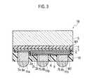
- FIG. 3is a cross-sectional view showing a schematic structure of an optical semiconductor device according to a second embodiment of the present invention.
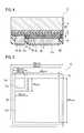
- FIG. 4is a cross-sectional view showing a schematic structure of an optical semiconductor device according to a third embodiment of the present invention.
- FIG. 5is a plan view showing the lower surface of the optical semiconductor device shown in FIG. 4 .
- FIG. 6is a cross-sectional view showing a schematic structure of an optical semiconductor device according to a fourth embodiment of the present invention.
- FIG. 7is a cross-sectional view showing a schematic structure of an optical semiconductor device according to a fifth embodiment of the present invention.
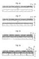
- FIG. 8is a first process cross-sectional view for illustrating a manufacturing method according to a sixth embodiment of the present invention.
- FIG. 9is a second process cross-sectional view.
- FIG. 10is a third process cross-sectional view.
- FIG. 11is a fourth process cross-sectional view.
- FIG. 12is a fifth process cross-sectional view.
- FIG. 13is a sixth process cross-sectional view.
- FIG. 14is a seventh process cross-sectional view.
- FIG. 15is an eighth process cross-sectional view.
- FIG. 16is a ninth process cross-sectional view.
- FIG. 17is a tenth process cross-sectional view.
- FIG. 18is an eleventh process cross-sectional view.
- FIG. 19is a twelfth process step cross-sectional view
- FIG. 20is a first process cross-sectional view for illustrating a manufacturing method according to a seventh embodiment of the present invention.
- FIG. 21is a second process cross-sectional view.
- FIG. 22is a third process cross-sectional view.
- FIG. 23is a fourth process cross-sectional view.
- FIG. 24is a first process cross-sectional view for illustrating a manufacturing method according to an eighth embodiment of the present invention.
- FIG. 25is a second process cross-sectional view.
- FIG. 26is a third process cross-sectional view.
- FIG. 27is a fourth process cross-sectional view.
- FIGS. 1 and 2With reference to FIGS. 1 and 2 , a first embodiment of the present invention will be described.
- an optical semiconductor device 1 Aincludes: a light-emitting layer 2 , an adhesive layer 3 , a fluorescent layer 4 , a light-transmissive layer 5 , a reflective layer 6 , a first electrode 7 a , multiple second electrodes 7 b , a first metal post 8 a , multiple second metal posts 8 b , an insulating layer 9 , a sealing layer 10 , a first metal layer 11 a and multiple second metal layers 11 b .
- the light-emitting layer 2has a first main surface M 1 and a second main surface M 2 .
- the adhesive layer 3 , the fluorescent layer 4 and the light-transmissive layer 5are sequentially provided on the first main surface M 1 .
- the reflective layer 6is provided on a first region of the second main surface M 2 of the light-emitting layer 2 .
- the first electrode 7 ais provided on a second region of the second main surface M 2 .
- the second electrodes 7 bare provided on the reflective layer 6 .
- the first metal post 8 ais provided on the first electrode 7 a .
- the second metal posts 8 bare provided on the respective second electrodes 7 b .
- the insulating layer 9is provided on regions, other than those with the metal posts 8 a and 8 b , of the second main surface M 2 of the light-emitting layer 2 .
- the sealing layer 10is provided on the insulating layer 9 so as to seal in the metal posts 8 a and 8 b .
- the first metal layer 11 ais provided on one end of the first metal post 8 a .
- the second metal layers 11 bare provided on one ends of the second metal posts 8 b , respectively.
- the light-emitting layer 2is formed of first and second cladding layers 2 a and 2 b , and an active layer 2 c .
- the first cladding layer 2 ais an n-type semiconductor layer.
- the second cladding layer 2 bis a p-type semiconductor layer, and is smaller in area than the first cladding layer 2 a .
- the active layer 2 cis held between the first and second cladding layers 2 a and 2 b .
- the light-emitting layer 2has a thickness of 5 ⁇ m, and is formed, for example, of InGaN layers that emit blue light. Note that the upper surface (in FIG. 1 ) of the first cladding layer 2 a serves as the first main surface M 1 , and the lower surface (in FIG. 1 ) of the second cladding layer 2 b and part of the lower surface (in FIG. 1 ) of the first cladding layer 2 a collectively serve as the second main surface M 2 , which has a step.
- the planar shape of the first cladding layer 2 ais a square 550 ⁇ m on a side (see the dotted line of FIG. 2 ).
- the second cladding layer 2 bis formed with the active layer 2 c interposed therebetween.
- the active layer 2 chas the same shape and approximately the same area as the second cladding layer 2 b.
- the adhesive layer 3is made of a silicone resin.
- the adhesive layer 3has a thickness not more than 1 ⁇ m, for example, and bonds the fluorescent layer 4 and the first main surface M 1 of the first cladding layer 2 a of the light-emitting layer 2 together.
- the silicone resinmethyl phenyl silicone having a refractive index of approximately 1.5 is used.
- a resin for sealing in phosphor particlesmethyl phenyl silicone or a silicone resin different in composition, such as dimethyl silicone, may be used. Alternatively, as long as appropriate for the intended use, another resin may be used.
- a resinsuch as an epoxy resin, a hybrid resin of an epoxy resin and a silicone resin, or a urethane resin may be used as the sealing resin.
- the fluorescent layer 4is formed by mixing phosphor particles in a silicone resin.
- the phosphor particlesconvert blue light into long-wavelength light.
- the fluorescent layer 4has a thickness of 15 ⁇ m, for example.
- the silicone resinmethyl phenyl silicone having a refractive index of approximately 1.5, which is also used for the adhesive layer 3 , is used.
- the silicone resin used for the fluorescent layer 4is not limited to this, but may be another resin.
- the phosphorused is YAG:Ce, which is yttrium aluminate doped with cerium as an activator and which has a particle diameter not more than 10 ⁇ m.
- the phosphor(Sr, Ba) 2 SiO 4 , which is strontium-barium silicate doped with europium as an activator, Ca p (Si, Al) 12 or the like may be used according to need.
- the mixed phosphorneed not necessarily be made of a material having a single composition, but may be made of a mixture of two materials: one for wavelength conversion from blue light into green light; the other for wavelength conversion from blue light into red light.
- the light-transmissive layer 5is made of a transparent substrate made of a material such as optical glass or quartz.
- the light-transmissive layer 5has a thickness of 200 ⁇ m, for example.
- the material of the light-transmissive layer 5is not limited to the transparent substrate, but may be another light-transmissive material.
- the light-transmissive layer 5needs only to be made of a light-transmissive substrate made of a light-transmissive inorganic material.
- a substrate having as a low refractive index as possible within a range from 1.0 to 2.0should preferably be used as the light-transmissive substrate. This reduces a difference in refractive index between the fluorescent layer 4 and the air, and thus can improve the light extraction efficiency of the optical semiconductor device 1 A.
- the reflective layer 6is made of a metal such as Ag or Al, and has a thickness of 0.3 ⁇ m, for example.
- the reflective layer 6is provided on the entire region (first region) of the lower surface (in FIG. 1 ) of the second cladding layer 2 b in the light-emitting layer 2 .
- an Ni/Au contact electrode(not shown) is formed by depositing metals such as Ni and Au in a thickness of 0.1 ⁇ m/0.1 ⁇ m on the lower surface of the second cladding layer 2 b , and the reflective layer 6 having a thickness of 0.3 ⁇ m is then formed thereon.
- the first electrode 7 ais formed by depositing metals such as Ni and Au in a thickness of 0.1 ⁇ m/0.1 ⁇ m, and thus has a thickness of 0.2 ⁇ m.
- the first electrode 7 awhich is formed in a circle having a diameter of 100 ⁇ m, is provided on an exposed region (second region) of the lower surface (in FIG. 1 ) of the first cladding layer 2 a in the light-emitting layer 2 (see FIG. 2 ).
- Each second electrode 7 bis also formed by depositing metals such as Ni and Au in a thickness of 0.1 ⁇ m/0.1 ⁇ m, and thus has a thickness of 0.2 ⁇ m.
- the second electrodes 7 beach of which is formed in a circle having a diameter of 100 ⁇ m, are provided on the lower surface (in FIG. 1 ) of the reflective layer 6 with a 200 ⁇ m pitch (see FIG. 2 ).
- the first metal post 8 ais formed of a metal such as Cu to have a columnar shape.
- the first metal post 8 ahas a height of approximately 103 ⁇ m and a diameter of 100 ⁇ m.
- a currentflows between the first metal post 8 a and the first electrode 7 a . Note that the shapes of the first electrode 7 a and the first metal post 8 a may be changed according to need.
- Each second metal post 8 bis formed of a metal such as Cu to have a columnar shape.
- the second metal post 8 bhas a height of approximately 100 ⁇ m and a diameter of 100 ⁇ m.
- a currentflows between the second metal post 8 b and the corresponding second electrode 7 b .
- the second metal posts 8 bare provided with a 200 ⁇ m pitch (see FIG. 2 ). Note that the shapes of the second electrodes 7 b and the second metal posts 8 b may be changed according to need.
- the insulating layer 9is made of SiO 2 , and functions as a passivation film (protective film).
- the insulating layer 9has a thickness of 0.3 ⁇ m.
- the insulating layer 9entirely covers the light-emitting layer 2 including the ends thereof, and thus prevents a current from flowing from the outside into the light-emitting layer 2 excluding the first and second electrodes 7 a and 7 b . This can prevent defects such as short circuit attributable to the phenomenon that mounting solder creeps up.
- the sealing layer 10is formed of a thermosetting resin, and has a thickness of approximately 100 ⁇ m like the metal posts 8 a and 8 b .
- the sealing layer 10is provided on the entire surface of the insulating layer 9 so as to seal in the first and second metal posts 8 a and 8 b while leaving one ends thereof exposed. Accordingly, the circumferential surface of each of the first and second metal posts 8 a and 8 b is completely covered with the sealing layer 10 .
- the insulating layer 9need not necessarily be provided in this manner.
- the sealing layer 10may be provided so as to entirely cover the light-emitting layer 2 including the ends thereof.
- a currentis prevented from flowing from the outside into the light-emitting layer 2 excluding the first and second electrodes 7 a and 7 b . Accordingly, defects such as short circuit attributable to the phenomenon that mounting solder creeps up can be prevented.
- Each of the first and second metal layers 11 a and 11 bis formed by depositing metals such as Ni and Au in a thickness of 0.1 ⁇ m/0.1 ⁇ m.
- the first metal layer 11 ais provided on the end, that is, the exposed portion, of the first metal post 8 a .
- Each second metal layer 11 bis provided on the end, that is, the exposed portion, of the corresponding second metal post 8 b .
- the first metal layer 11 ahas the same circular planar shape as the first electrode 7 a
- each second metal layer 11 bhas the same circular planar shape as each second electrode 7 b (see FIG. 2 ).
- the resultant potentialis supplied to the first cladding layer 2 a through the first metal post 8 a
- the resultant potentialis supplied to the second cladding layer 2 b through the second metal posts 8 b .
- light beamsare emitted from the active layer 2 c held between the first and second cladding layers 2 a and 2 b .
- Some of the emitted light beamsare transmitted through the light-transmissive layer 5 , and emitted from the surface of the light-transmissive layer 5 without reflection.
- Some of the emitted light beamsare reflected by the reflective layer 6 , then transmitted through the light-transmissive layer 5 , and emitted from the surface of the light-transmissive layer 5 . Others are incident on the phosphor particles included in the fluorescent layer 4 , so that the phosphor particles are excited to emit light beams. Some of the light beams emitted from the phosphor particles are also transmitted through the light-transmissive layer 5 , and emitted from the surface of the light-transmissive layer 5 . Others are also reflected by the reflective layer 6 , then transmitted through the light-transmissive layer 5 , and emitted from the surface of the light-transmissive layer 5 .
- the blue light beams emitted from the light-emitting layer 2 and the (yellow, or red and green) light beams emitted from the phosphor particles that are excited by the blue light beamsare mixed into white light, which is emitted from the surface of the light-transmissive layer 5 .
- the optical semiconductor device 1 Ais simplified in configuration, and miniaturized to have a plane area as small as that of the light-emitting layer 2 .
- the structureeliminates the need for molding, a mounting step and a connecting step in manufacturing the optical semiconductor device 1 A. Accordingly, the optical semiconductor device 1 A can be manufactured by using normal semiconductor manufacturing equipment, and thus can be manufactured at reduced cost.
- the fluorescent layer 4 for wavelength conversion from blue light into long-wavelength lightis formed on the light-emitting layer 2
- the reflective layer 6is formed under the lower surface of the light-emitting layer 2 (in FIG. 1 ).
- the light-emitting layer 2by causing the light-emitting layer 2 to emit blue light only upward, white light can be emitted toward the top surface (in FIG. 1 ) of the optical semiconductor device 1 A.
- the light-transmissive layer 5 formed on the fluorescent layer 4reduces the refractive index difference between the fluorescent layer 4 and the air, which allows the optical semiconductor device 1 A to have improved light extraction efficiency.
- the above-mentioned structureallows the optical semiconductor device 1 A, which has a plane area as small as that of the light-emitting layer 2 , to be reliably mounted on a glass epoxy board, which is a typical wiring board. This is because the metal posts 8 a and 8 b reduce the linear expansion coefficient difference between the light-emitting layer 2 and the glass epoxy board.
- the optical semiconductor device 1 A having the above-described structureis obtained as follows. Firstly, the fluorescent layer 4 is provided on the light-emitting layer 2 , and a light-transmissive inorganic material is then deposited on the fluorescent layer 4 so as to serve as the light-transmissive layer 5 . Thereafter, the first metal post 8 a is provided on the first electrode 7 a of the light-emitting layer 2 , and the second metal posts 8 b are provided on the respective second electrodes 7 b of the light-emitting layer 2 . Then, the sealing layer 10 is provided on the light-emitting layer 2 so as to seal in the first and second metal posts 8 a and 8 b .
- the light-transmissive layer 5is made of an inorganic material, and thus prevented from being degraded by light (blue light, in particular) emitted from the light-emitting layer 2 . Accordingly, the life reduction of the optical semiconductor device 1 A is suppressed.
- the optical semiconductor device 1 Amay be manufactured at reduced cost. Accordingly, cost reduction of the optical semiconductor device 1 A can be achieved.
- the optical semiconductor device 1 Acan be miniaturized approximately to the size of a typical optical semiconductor element.
- the first metal layer 11 a and the second metal layers 11 bare solder bumps.
- a hemispherical solder bump having a diameter of 100 ⁇ mis formed on each of the first and second metal posts 8 a and 8 b .
- the solder bumpis made of a solder material used for surface mounting, such as Sn-3.0Ag-0.5Cu, Sn-0.8Cu and Sn-3.5Ag.
- the second embodiment of the present inventioncan provide the same effects as the first embodiment. Moreover, since the first metal layer 11 a and the second metal layers 11 b are formed of solder bumps, the optical semiconductor device 1 B has a larger gap from a wiring board on which the optical semiconductor device 1 B is mounted than the optical semiconductor device 1 A according to the first embodiment. Accordingly, when the optical semiconductor device 1 B is mounted on the wiring board, a stress attributable to the linear expansion coefficient difference between the optical semiconductor device 1 B and the wiring board can be further reduced.
- FIGS. 4 and 5a third embodiment of the present invention will be described.
- the same parts as those in the first embodimentare denoted by the same reference numerals, and the description thereof is omitted.
- the first electrode 7 ais formed as a square 100 ⁇ m on a side on the lower surface (in FIG. 4 ) of the first cladding layer 2 a .
- the second electrode 7 bis formed as a square 500 ⁇ m on a side with a square 150 ⁇ m on a side cut out. Specifically, the cutout portion corresponds to the corner region of the first cladding layer 2 a .
- the first metal post 8 ais a rectangular column having the same planar shape as the first electrode 7 a
- the second metal post 8 bis a rectangular column having the same planar shape as the second electrode 7 b
- the first metal layer 11 ahas the same planar shape as the first electrode 7 a
- the second metal layer 11 bhas the same planar shape as the second electrode 7 b (see FIG. 5 ).
- the third embodiment of the present inventioncan provide the same effects as the first embodiment. Moreover, in the optical semiconductor device 1 C according to the third embodiment, the plane area of each of the first and second electrodes 7 a and 7 b is increased, and thus the plane area of each of the first and second metal posts 8 a and 8 b is increased, compared to the optical semiconductor device 1 A according to the first embodiment. This expands heat dissipation paths for allowing heat generated during light emission to escape from the optical semiconductor device 1 C, and thus reduces thermal resistance thereof. This allows the optical semiconductor device 1 C to generate a reduced amount of heat during the passage of a current, and to have a greatly reduced transient thermal resistance.
- a fourth embodiment of the present inventionwill be described.
- the same parts as those in the first embodimentare denoted by the same reference numerals, and the description thereof is omitted.
- an optical semiconductor device 1 Ddoes not include the adhesive layer 3 , and the fluorescent layer 4 is formed directly on the first main surface M 1 of the light-emitting layer 2 .
- the fluorescent layer 4has a thickness of 10 ⁇ m, and is formed on the first main surface M 1 of the light-emitting layer 2 by a method such as sputtering or chemical vapor deposition (CVD).
- the light-transmissive layer 5is formed on the fluorescent layer 4 by, for example, applying a liquid glass onto the fluorescent layer 4 by spin coating, and then hardening the liquid glass.
- the fourth embodiment of the present inventioncan provide the same effects as the first embodiment. Moreover, the above-described structure can eliminate, from the manufacturing process, a step of blending phosphor particles with a silicone resin and a step of bonding the fluorescent layer 4 onto the light-emitting layer 2 , both of which are needed in the manufacturing process of the optical semiconductor device 1 A according to the first embodiment. Thus, the fourth embodiment can reduce the manufacturing process time and the cost.
- a fifth embodiment of the present inventionwill be described.
- the same parts as those in the first embodimentare denoted by the same reference numerals, and the description thereof is omitted.
- an optical semiconductor devicedoes not include the adhesive layer 3 , and the fluorescent layer 4 is formed directly on the first main surface M 1 of the light-emitting layer 2 .
- the fluorescent layer 4consists of two layers, namely, fluorescent layers 4 a and 4 b respectively made of materials mutually different in composition. Specifically, on the light-emitting layer 2 , sequentially formed are the fluorescent layer 4 a for wavelength conversion from blue light into green light, and the fluorescent layer 4 b for wavelength conversion from blue light into red light.
- Each of the fluorescent layers 4 a and 4 bhas a thickness of 10 ⁇ m, and is formed on the first main surface M 1 of the light-emitting layer 2 by a method such as sputtering or chemical vapor deposition (CVD).
- the light-transmissive layer 5is formed on the fluorescent layer 4 by, for example, applying a liquid glass onto the fluorescent layer 4 b by spin coating, and then hardening the liquid glass.
- the fifth embodiment of the present inventioncan provide the same effects as the first embodiment. Moreover, the above-described structure can eliminate, from the manufacturing process, a step of blending phosphor particles with a silicone resin and a step of bonding the fluorescent layer 4 onto the light-emitting layer 2 , both of which are needed in the manufacturing process of the optical semiconductor device 1 A according to the first embodiment. Thus, the fifth embodiment can reduce the manufacturing process time and the cost.
- a sixth embodiment of the present inventionwill be described.
- a method for manufacturing the optical semiconductor device 1 A according to the first embodimentwill be described. Note that this manufacturing method can be used as a method for manufacturing the optical semiconductor device 1 C according to the third embodiment.
- the same parts as those in the first embodimentare denoted by the same reference numerals, and the description thereof is omitted.
- InGaN light-emitting layers 12 that emit blue lightare formed on a substrate 11 , which is a sapphire wafer having a diameter of two inches and a thickness of 200 ⁇ m.
- a light-emitting layeris formed by epitaxial growth, and then separated into the light-emitting layers 12 by reactive ion etching (RIE). In this way, the light-emitting layer 2 of the optical semiconductor device 1 A is formed.
- RIEreactive ion etching
- the light-emitting layer 2is formed by forming the first cladding layer 2 a on a square region 550 ⁇ m on a side, and then forming the second cladding layer 2 b on a region, not including a corner region (a square 150 ⁇ m on a side), of the lower surface of the first cladding layer 2 a with the active layer 2 c interposed therebetween (see FIGS. 1 and 2 ).
- multi-layer films 13are formed on the respective light-emitting layers 12 on the substrate 11 .
- Ni/Au films (not shown) having a thickness of 0.1 ⁇ m/0.1 ⁇ mare firstly formed on the entire surfaces of the light-emitting layers 12 by sputtering so as to serve as contact layers of the light-emitting layers 12 , respectively.
- metal films (not shown) made of Ag or Al and having a thickness of 0.3 ⁇ mare formed on the respective Ni/Au films by sputtering. In this way, the reflective layer 6 of the optical semiconductor device 1 A is formed.
- Ni/Au films(not shown) having a thickness of 0.1 ⁇ m/0.1 ⁇ m, which are to be formed into electrodes, are respectively formed on electrode portions of the light-emitting layers 12 .
- SiO 2 passivation films(not shown) having a thickness of 0.3 ⁇ m are formed by sputtering on regions other than the electrode portions of the light-emitting layers 12 .
- the first electrode 7 a , the second electrodes 7 b and the insulating layer 9 of the optical semiconductor device 1 Aare formed.
- the multi-layer films 13are formed on the respective light-emitting layers 12 on the substrate 11 .
- a seed layer 14which is a conductive film serving as a power feeding layer for plating, is formed on the entire surface of the substrate 11 by a physical deposition method such as vapor deposition or sputtering.
- a multi-layer filmsuch as a Ti/Cu film is used.
- the Ti/Cu filmwhich is formed to increase adhesion strength between the seed layer 14 and a resist or pads, needs only to have a thickness as small as 0.1 ⁇ m.
- the Cu layerwhich mainly contributes to power feeding, should preferably have a thickness not smaller than 0.2 ⁇ m.
- a resist layer 15 serving as a sacrifice layeris formed on the entire surface of the substrate 11 .
- the resist layer 15has openings at electrode pad portions which are to be formed into the first and second electrodes 7 a and 7 b .
- a photosensitive liquid resist or a dry film resistmay be used as the resist.
- the resist layer 15is formed on the entire surface of the substrate 11 by forming a resist layer on the substrate 11 , and then forming the openings in this resist layer by exposure and development using a light shield mask. After development, the resist may be baked depending on its material.
- plated layers 16are formed by electroplating in the respective openings of the resist layer 15 .
- the metal posts 8 a and 8 b of the optical semiconductor device 1 Aare formed.
- the substrate 11which is a wafer, is immersed in a plating liquid consisting of materials such as copper sulphate and sulphuric acid. Under this condition, current is caused to flow through the substrate 11 by connecting the seed layer 14 to the negative terminal of a direct-current power source, and connecting a Cu plate, serving as an anode, to the positive terminal of the direct-current power source, and thus Cu plating starts.
- the Cu plateis placed so as to face the to-be-plated surface of the substrate 11 . Before the thickness of the plated layer, which increases with time, reaches that of the resist layer 15 , the current is stopped, and thus the plating is completed.
- the resist layer 15is peeled off the substrate 11 , and then the seed layer 14 is etch removed by acid cleaning. Thereby, the light-emitting layers 12 , the multi-layer films 13 and the plated layers 16 are exposed.
- thermosetting resin layer 17 to serve as a sealing layeris formed on the entire surface of the substrate 11 .
- a thermosetting resinis applied by spin coating around the plated layers 16 in a thickness to allow the plated layers 16 embedded therein.
- the resultant substrate 11is put in an oven and heated, and thus the thermosetting resin layer 17 is hardened.
- the resincan be hardened by being heated at 150° C. for two hours, for example.
- thermosetting resin layer 17is ground off so that ends of the respective plated layers 16 can be exposed.
- the thermosetting resin layer 17is grounded by rotational grinding using a rotational grinding wheel, and thus the surface thereof can be planarized after being ground.
- the substrate 11may be dried according to need. Note that, in the previous step, it is difficult to apply a thermosetting resin by a method such as spin coating with only the ends of the plated layers 16 exposed (It requires much time and cost). Accordingly, this grinding step is necessary for exposing the ends of the plated layers 16 after the spin coating step.
- the light-emitting layersare lifted off the substrate 11 by irradiating the interface between the substrate 11 and the light-emitting layers 12 with laser beams.
- a light-emitting substrate 12 A formed of the light-emitting layers 12 , the multi-layer films 13 , the plated layers 16 and the thermosetting resin layer 17is separated off the substrate 11 .
- the light-emitting layers 12are lifted off the substrate 11 by causing an Nd:YAG third harmonic laser to irradiate the interface therebetween with laser beams having a wavelength of 355 nm through the substrate 11 .
- the liftoff stepis optional, and thus may be omitted.
- the surface, at which the light-emitting layers 12 are exposed, of the light-emitting substrate 12 A formed by this liftoff stepis bonded onto a fluorescent layer 19 that is provided on a light-transmissive substrate 18 , such as an optical glass wafer with an adhesive layer 20 interposed therebetween.
- This fluorescent substrate on which the light-emitting substrate 12 A is bondedis formed in another step. Specifically, a silicone resin layer mixed with phosphor particles is formed as the fluorescent layer 19 on the light-transmissive substrate 18 made of a light-transmissive inorganic material, and another silicone resin layer is formed as the adhesive layer 20 on the silicone resin layer. In this way, the light-transmissive layer 5 , the fluorescent layer 4 and the adhesive layer 3 of the optical semiconductor device 1 A are formed.
- the phosphor particles and the silicone resinare uniformly mixed using a rotary and revolutionary mixer, and then applied onto the light-transmissive substrate 18 by spin coating.
- the resultant light-transmissive substrate 18is put in an oven, and the silicone resin is hardened therein.
- the silicone resin used herecan be hardened by being heated at 150° C. for an hour, for example.
- the silicone resinis hardened with spacers formed thereon, and with jigs having anti-sticking surfaces coated with fluorine attached thereon. Thereby, the curvature of the surface of the silicone resin film attributable to surface tension can be suppressed, and thus the silicone resin film having a uniform thickness can be formed.
- the light-emitting layers 12are bonded onto the fluorescent layer 19 , which is a silicone resin layer mixed with phosphor particles, as follows. Firstly, a silicone resin is applied onto the fluorescent layer 19 (or the light-emitting layers 12 ) by spraying. After that, the light-emitting substrate 12 A appropriately positioned and stacked on the light-transmissive substrate 18 . The light-emitting substrate 12 A and the light-transmissive substrate 18 thus stacked are put into an oven, and bonded together by hardening the silicone resin therein.
- the silicone resincan be hardened by being heated at 150° C. for an hour, for example.
- Ni/Au layers 21are formed by electroless plating on the respective plated layers 16 to serve as Cu electrodes.
- the metal layers 11 a and 11 b of the optical semiconductor device 1 Aare formed.
- the waferis firstly degreased by, for example, being treated with a slightly alkaline degreasing liquid for three minutes, and is then washed with running water for one minute. Thereafter, the wafer is acid cleaned, and then immersed in a nickel-phosphorus plating liquid at liquid temperature adjusted to 70° C. Thereafter, the wafer is washed with water, and thus the Ni layers are formed.
- the waferis immersed in an electroless gold plating liquid at liquid temperature adjusted to 70° C. Thereafter, the wafer is washed with water and then dried. In this way, the surfaces of the respective Cu electrodes are plated.
- the resultant stackis diced into the multiple optical semiconductor devices 1 A using a dicer.
- the optical semiconductor device 1 A according to the first embodimentis obtained.
- approximately the same steps as aboveare employed in the manufacturing process of the optical semiconductor device 1 C according to the third embodiment.
- the optical semiconductor device 1 C according to the third embodimentcan be obtained.
- the optical semiconductor device 1 A according to the first embodimentcan be manufactured.
- the sixth embodimentcan provide the same effects as the first embodiment.
- the optical semiconductor device 10 according to the third embodimentcan be manufactured.
- the sixth embodimentcan provide the same effects as the third embodiment.
- the sixth embodimentallows a large number of optical semiconductor devices 1 A or 1 C to be manufactured through a single manufacturing process, and thus allows mass production of the optical semiconductor devices 1 A or 1 C. Therefore, the sixth embodiment can suppress the costs of the optical semiconductor devices 1 A and 1 C.
- a seventh embodiment of the present inventionwill be described.
- a method for manufacturing the optical semiconductor device 1 B according to the second embodimentwill be described. Note that, in the seventh embodiment, the same parts as those in the second embodiment are denoted by the same reference numerals, and the description thereof is omitted.
- the manufacturing process according to the seventh embodiment of the present inventionhas the same steps as those in the sixth embodiment from the step of forming the light-emitting layers 12 shown in FIG. 8 to the bonding step shown in FIG. 17 .
- contact layers 31such as Ni/Au layers are formed on by electroless plating on the respective plated layers 16 to serve as Cu electrodes.
- contact layers 31such as Ni/Au layers are formed on by electroless plating on the respective plated layers 16 to serve as Cu electrodes.
- Ni electroless plating and Au electroless platingthe same processes are performed as those in the step of forming the Ni/Au layers 21 according to the sixth embodiment.
- solder paste 32 made of Sn-3.0Ag-0.5Cuis applied onto the contact layers 31 by printing. Note that the method for applying the solder paste 32 is not limited to printing.
- the light-transmissive substrate 18which is a wafer, is passed through a reflow furnace.
- the solderis remelted and a flux residue is cleaned off.
- solder bumps 33are formed on the respective plated layers 16 to serve as Cu electrodes. In this way, the metal layers 11 a and 11 b of the optical semiconductor device 1 B are formed.
- the resultant stackis diced into the multiple optical semiconductor devices 1 B using a dicer. In this way, the optical semiconductor device 1 B according to the second embodiment is obtained.
- the optical semiconductor device 1 B according to the second embodimentcan be manufactured.
- the seventh embodimentcan provide the same effects as the second embodiment.
- the seventh embodimentallows a large number of optical semiconductor devices 1 B to be manufactured through a single manufacturing process, and thus allows mass production of the optical semiconductor devices 1 B. Therefore, the seventh embodiment can suppress the costs of the optical semiconductor devices 1 B.
- an eighth embodiment of the present inventionwill be described.
- a method for manufacturing the optical semiconductor device 1 D according to the fourth embodimentwill be described. Note that this manufacturing method can be used as a method for manufacturing the optical semiconductor device 1 E according to the fifth embodiment.
- the same parts as those in the fourth embodimentare denoted by the same reference numerals, and the description thereof is omitted.
- the manufacturing process according to the eighth embodiment of the present inventionhas the same steps as those in the sixth embodiment from the step of forming the light-emitting layers 12 shown in FIG. 8 to the liftoff step shown in FIG. 16 .
- a fluorescent layer 41is formed on the surface, at which the light-emitting layers 12 are exposed, of the light-emitting substrate 12 A, by using a sputtering apparatus.
- the fluorescent layer 4 of the optical semiconductor device 1 Dis formed.
- the fluorescent layer 41may be formed to have a multi-layer structure by performing sputtering multiple times.
- the fluorescent layer 4 of the optical semiconductor device 1 E according to the fifth embodimentcan be formed.
- the fluorescent layer 41may alternatively be formed using a CVD apparatus.
- a liquid glassis applied onto the fluorescent layer 41 by spin coating, and then hardened. Thereby, a light-transmissive layer 42 is formed on the fluorescent layer 41 . In this way, the light-transmissive layer 5 of the optical semiconductor device 1 D is formed.
- the method for applying the liquid glassmay be spraying, and does not particularly limited.
- the glass layercan be hardened by being heated at 200° C. for an hour, for example.
- any materialmay be used for the light-transmissive layer 42 according to need.
- Ni/Au layers 43are formed on by electroless plating on the respective plated layers to serve as Cu electrodes.
- the metal layers 11 a and 11 b of the optical semiconductor device 1 Dare formed.
- Ni electroless plating and Au electroless platingthe same processes are performed as those in the step of forming the Ni/Au layers 21 according to the sixth embodiment.
- the resultant stackis diced into the multiple optical semiconductor devices 1 D using a dicer.
- the optical semiconductor device 1 D according to the fourth embodimentis obtained.
- approximately the same steps as aboveare employed in the manufacturing process of the optical semiconductor device 1 E according to the fifth embodiment.
- the optical semiconductor device 1 E according to the fifth embodimentcan be obtained.
- the optical semiconductor device 1 D according to the fourth embodimentcan be manufactured.
- the eighth embodimentcan provide the same effects as the fourth embodiment.
- the optical semiconductor device 1 E according to the fifth embodimentcan be manufactured.
- the eighth embodimentcan provide the same effects as the fifth embodiment.
- the sixth embodimentallows a large number of optical semiconductor devices 1 D or 1 E to be manufactured through a single manufacturing process, and thus allows mass production of the optical semiconductor devices 1 D or 1 E. Therefore, the eighth embodiment can suppress the costs of the optical semiconductor devices 1 D and 1 E.
- the present inventionis not limited to the foregoing embodiments, and may be variously changed without departing from the gist of the present invention.
- some of the components shown in the foregoing embodimentsmay be omitted.
- the components in different ones of the embodimentsmay be used in combination according to need.
- specific values used in the foregoing embodimentsare only examples, and thus the present invention is not limited to these.
Landscapes
- Led Device Packages (AREA)
- Led Devices (AREA)
Abstract
Description
- This application is based on and claims the benefit of priority from Japanese Patent Application No. 2008-312453, filed on Dec. 8, 2008; the entire contents of which are incorporated herein by reference.
- 1. Field of the Invention
- The present invention relates to an optical semiconductor device and a method for manufacturing the same.
- 2. Description of the Related Art
- In response to the development of a high-intensity optical semiconductor element that emits blue light, there has been commercialized an optical semiconductor device that emits white light by using an optical semiconductor element that emits blue light and a phosphor capable of wavelength conversion from blue light into yellow light. Such an optical semiconductor device that emits white light has characteristics of: being small in size; emitting high-intensity light relative to a supplied power amount; having a long life; and using no toxic substance such as mercury. These characteristics allow the optical semiconductor device to be increasingly used in various fields such as application to an under-button light source or a flash light source for portable phone and application to an interior light source and an exterior light source for vehicle.
- In terms of total flux relative to a supplied power amount, an optical semiconductor device using blue LEDs currently has an efficiency of 150 μm/W, which is larger than those of conventional light sources such as an incandescent light bulb (15 μm/W to 20 μm/W) and a fluorescent lamp (60 μm/W to 90 μm/W). However, in terms of cost required for one lm, the optical semiconductor device has a problem of requiring cost more than ten times higher than the conventional light sources which require 0.1 yen/lm to 0.2 yen/lm. As a measure to reduce the cost, there has been studied a structure of an optical semiconductor device allowing cost reduction while enhancing the luminous efficiency of an element therein.
- The most general optical semiconductor device that has been commercialized has a structure including: an optical semiconductor element that emits blue light; an Ag-plated Cu frame formed of a white thermoplastic resin by molding, and used as a wiring board; a connection material for connecting the optical semiconductor element and the frame; a gold wire through which a current flows between the frame and a top surface electrode of the optical semiconductor element; and a silicone resin mixed with phosphor particles for wavelength conversion from blue light into yellow light and sealing in the optical semiconductor element (see JP-A No. 2000-183407 (KOKAI), for example).
- In manufacturing this optical semiconductor device, a white thermoplastic resin is firstly formed into the Ag-plated Cu frame by molding. Then, a connection resin is applied onto a portion, on which the optical semiconductor element is to be mounted, of the frame. Thereafter, the optical semiconductor element is mounted on the portion, and the connection resin is hardened by heating in an oven. Thereby, the optical semiconductor element is connected to the frame. Then, by using a wire bonder, the electrode formed on the chip top surface of the optical semiconductor element is connected to the frame with an Au wire. Thereafter, a silicone resin with a phosphor concentration adjusted to allow the optical semiconductor device to emit white light is applied, by a dispense technique, around the portion in which the optical semiconductor element is mounted, and then hardened by heating. Lastly, a product portion including the optical semiconductor element is cut off, and the frame used as an exterior electrode is finished by a forming process. Thereby, the optical semiconductor device is completed.
- As described above, a conventional optical semiconductor device is manufactured by incorporating a blue light semiconductor element in a structure of an optical semiconductor device that, in most cases, has been commercialized using an optical semiconductor element that emits light having a wavelength of 500 nm or more. The optical semiconductor device that emits such long-wavelength light has a high directivity and has thus been applied to devices for vehicle, display panels, amusement machines and the like.
- Such a conventional optical semiconductor device manufactured as above has a problem of having a shorter life for reasons, such as that blue light, which has a short wavelength and a high intensity, discolors a reflector resin having benzene ring. In addition, an optical semiconductor device that emits white light commercialized in response to the development of a high-intensity optical semiconductor element that emits blue light has been increasingly applied to lighting apparatuses as well as conventionally-applied apparatuses such as devices for vehicle and display panels. With this trend, cost reduction of the optical semiconductor device has been indispensably required. However, the conventional structure of an optical semiconductor device only allows limited cost reduction, and thus the structure and the manufacturing process of the optical semiconductor device has been required to be reconsidered.
- In addition, when an optical semiconductor device is applied to a lighting apparatus, a light source therein cannot be formed of a single optical semiconductor device. Accordingly, in order to replace a general lighting apparatus, such as a fluorescent lamp, with an apparatus using an optical semiconductor device that emits white light, the apparatus needs to include multiple optical semiconductor devices. In this case, to eliminate defects such as nonuniform intensity in a light-emitting surface, a large number of small optical semiconductor devices need to be mounted on a wiring board. Accordingly, the size reduction of the optical semiconductor device has also been required.
- An object of the present invention is to provide an optical semiconductor device that is capable of suppressing the life reduction thereof, that can be manufactured at reduced cost, and that can be miniaturized approximately to the size of an optical semiconductor element, and to provide a method for manufacturing such an optical semiconductor device.
- A first aspect according to an embodiment of the present invention is an optical semiconductor device includes: a light-emitting layer having a first main surface, a second main surface opposed to the first main surface, a first electrode and a second electrode which are formed on the second main surface; a fluorescent layer containing phosphor particles and provided on the first main surface; a light-transmissive layer provided on the fluorescent layer and made of a light-transmissive inorganic material; a first metal post provided on the first electrode; a second metal post provided on the second electrode; a sealing layer provided on the second main surface so as to seal in the first and second metal posts with one ends of the respective first and second metal posts exposed; a first metal layer provided on the exposed end of the first metal post; and a second metal layer provided on the exposed end of the second metal post.
- A second aspect according to an embodiment of the present invention is a method for manufacturing an optical semiconductor device, includes: manufacturing a light-emitting substrate by forming multiple groups of positive and negative electrodes on a first main surface of a light-emitting layer, the positive and negative electrodes being used to cause a current for exciting the light-emitting layer to flow through the light-emitting layer; manufacturing a fluorescent substrate by forming, on a light-transmissive inorganic film, a fluorescent layer made of a resin in which phosphor particles are dispersed; bonding the fluorescent layer of the fluorescent substrate onto a second main surface of the light-emitting layer which is opposed to the first main surface; and separating the bonded substrate into pieces each including one of the groups of the positive and negative electrodes.
- A third aspect according to an embodiment of the present invention is a method for manufacturing an optical semiconductor device, includes: forming multiple light-emitting layers on a substrate, the light-emitting layers each having a first main surface, a second main surface opposed to the first main surface, a first electrode and a second electrode which are formed on the second main surface; forming a conductive film on the substrate, on which the multiple light-emitting layers are formed, so that the conductive film covers the multiple light-emitting layers; forming a sacrifice layer on the conductive film, the sacrifice layer having openings located respectively on the first and second electrodes of all of the light-emitting layers; forming plated layers respectively on the first and second electrodes of all of the light-emitting layers by electroplating using the conductive film as a negative electrode; removing the sacrifice layer and the conductive film from the substrate on which the plated layers are formed; forming a sealing layer on the substrate from which the sacrifice layer and the conductive film are removed, the sealing layer sealing in the plated layers of all of the light-emitting layers; exposing one ends of the respective plated layers of all of the light-emitting layers from the sealing layer; forming a fluorescent layer containing phosphor particles on a light-transmissive substrate made of a light-transmissive inorganic material; bonding the fluorescent layer formed on the light-transmissive substrate onto all of the light-emitting layers; forming metal layers respectively on the exposed ends of the plated layers of all of the light-emitting layers; and separating the resultant substrate into pieces each including one of the light-emitting layers.
- A fourth aspect according to an embodiment of the present invention is a method for manufacturing an optical semiconductor device, includes: forming multiple light-emitting layers on a substrate, the light-emitting layers each having a first main surface, a second main surface opposed to the first main surface, a first electrode and a second electrode which are formed on the second main surface; forming a conductive film on the substrate, on which the multiple light-emitting layers are formed, so that the conductive film covers the multiple light-emitting layers; forming a sacrifice layer on the conductive film, the sacrifice layer having openings located respectively on the first and second electrodes of all of the light-emitting layers; forming plated layers respectively on the first and second electrodes of all of the light-emitting layers by electroplating using the conductive film as a negative electrode; removing the sacrifice layer and the conductive film from the substrate on which the plated layers are formed; forming a sealing layer on the substrate from which the sacrifice layer and the conductive film are removed, the sealing layer sealing in the plated layers of all of the light-emitting layers; exposing one ends of the respective plated layers of all of the light-emitting layers from the sealing layer; forming a fluorescent layer containing phosphor particles on all of the light-emitting layers; forming a light-transmissive layer made of a light-transmissive inorganic material on the fluorescent layer; forming metal layers respectively on the exposed ends of the plated layers of all of the light-emitting layers; and separating the resultant substrate into pieces each including one of the light-emitting layers.
FIG. 1 is a cross-sectional view showing a schematic structure of an optical semiconductor device according to a first embodiment of the present invention.FIG. 2 is a plan view showing the lower surface of the optical semiconductor device shown inFIG. 1 .FIG. 3 is a cross-sectional view showing a schematic structure of an optical semiconductor device according to a second embodiment of the present invention.FIG. 4 is a cross-sectional view showing a schematic structure of an optical semiconductor device according to a third embodiment of the present invention.FIG. 5 is a plan view showing the lower surface of the optical semiconductor device shown inFIG. 4 .FIG. 6 is a cross-sectional view showing a schematic structure of an optical semiconductor device according to a fourth embodiment of the present invention.FIG. 7 is a cross-sectional view showing a schematic structure of an optical semiconductor device according to a fifth embodiment of the present invention.FIG. 8 is a first process cross-sectional view for illustrating a manufacturing method according to a sixth embodiment of the present invention.FIG. 9 is a second process cross-sectional view.FIG. 10 is a third process cross-sectional view.FIG. 11 is a fourth process cross-sectional view.FIG. 12 is a fifth process cross-sectional view.FIG. 13 is a sixth process cross-sectional view.FIG. 14 is a seventh process cross-sectional view.FIG. 15 is an eighth process cross-sectional view.FIG. 16 is a ninth process cross-sectional view.FIG. 17 is a tenth process cross-sectional view.FIG. 18 is an eleventh process cross-sectional view.FIG. 19 is a twelfth process step cross-sectional viewFIG. 20 is a first process cross-sectional view for illustrating a manufacturing method according to a seventh embodiment of the present invention.FIG. 21 is a second process cross-sectional view.FIG. 22 is a third process cross-sectional view.FIG. 23 is a fourth process cross-sectional view.FIG. 24 is a first process cross-sectional view for illustrating a manufacturing method according to an eighth embodiment of the present invention.FIG. 25 is a second process cross-sectional view.FIG. 26 is a third process cross-sectional view.FIG. 27 is a fourth process cross-sectional view.- With reference to
FIGS. 1 and 2 , a first embodiment of the present invention will be described. - As shown in
FIG. 1 , anoptical semiconductor device 1A according to the first embodiment of the present invention includes: a light-emittinglayer 2, an adhesive layer3, afluorescent layer 4, a light-transmissive layer 5, areflective layer 6, afirst electrode 7a, multiplesecond electrodes 7b, afirst metal post 8a, multiplesecond metal posts 8b, an insulatinglayer 9, asealing layer 10, afirst metal layer 11aand multiple second metal layers11b. The light-emittinglayer 2 has a first main surface M1 and a second main surface M2. The adhesive layer3, thefluorescent layer 4 and the light-transmissive layer 5 are sequentially provided on the first main surface M1. Thereflective layer 6 is provided on a first region of the second main surface M2 of the light-emittinglayer 2. Thefirst electrode 7ais provided on a second region of the second main surface M2. Thesecond electrodes 7bare provided on thereflective layer 6. Thefirst metal post 8ais provided on thefirst electrode 7a. Thesecond metal posts 8bare provided on the respectivesecond electrodes 7b. The insulatinglayer 9 is provided on regions, other than those with themetal posts layer 2. Thesealing layer 10 is provided on the insulatinglayer 9 so as to seal in themetal posts first metal layer 11ais provided on one end of thefirst metal post 8a. The second metal layers11bare provided on one ends of thesecond metal posts 8b, respectively. - The light-emitting
layer 2 is formed of first and second cladding layers2aand2b, and anactive layer 2c. Thefirst cladding layer 2ais an n-type semiconductor layer. Thesecond cladding layer 2bis a p-type semiconductor layer, and is smaller in area than thefirst cladding layer 2a. Theactive layer 2cis held between the first and second cladding layers2aand2b. The light-emittinglayer 2 has a thickness of 5 μm, and is formed, for example, of InGaN layers that emit blue light. Note that the upper surface (inFIG. 1 ) of thefirst cladding layer 2aserves as the first main surface M1, and the lower surface (inFIG. 1 ) of thesecond cladding layer 2band part of the lower surface (inFIG. 1 ) of thefirst cladding layer 2acollectively serve as the second main surface M2, which has a step. - As shown in
FIG. 2 , the planar shape of thefirst cladding layer 2ais a square 550 μm on a side (see the dotted line ofFIG. 2 ). On a region, not including a corner region (a square 150 μm on a side), of the lower surface (inFIG. 1 ) of thefirst cladding layer 2a, thesecond cladding layer 2bis formed with theactive layer 2cinterposed therebetween. Theactive layer 2chas the same shape and approximately the same area as thesecond cladding layer 2b. - The adhesive layer3 is made of a silicone resin. The adhesive layer3 has a thickness not more than 1 μm, for example, and bonds the
fluorescent layer 4 and the first main surface M1 of thefirst cladding layer 2aof the light-emittinglayer 2 together. Specifically, as the silicone resin, methyl phenyl silicone having a refractive index of approximately 1.5 is used. As a resin for sealing in phosphor particles, methyl phenyl silicone or a silicone resin different in composition, such as dimethyl silicone, may be used. Alternatively, as long as appropriate for the intended use, another resin may be used. For example, when theoptical semiconductor device 1A has a low luminance and thus the sealing resin will not be degraded by blue light, a resin such as an epoxy resin, a hybrid resin of an epoxy resin and a silicone resin, or a urethane resin may be used as the sealing resin. - The
fluorescent layer 4 is formed by mixing phosphor particles in a silicone resin. The phosphor particles convert blue light into long-wavelength light. Thefluorescent layer 4 has a thickness of 15 μm, for example. As the silicone resin, methyl phenyl silicone having a refractive index of approximately 1.5, which is also used for the adhesive layer3, is used. However, the silicone resin used for thefluorescent layer 4 is not limited to this, but may be another resin. Meanwhile, as the phosphor, used is YAG:Ce, which is yttrium aluminate doped with cerium as an activator and which has a particle diameter not more than 10 μm. Alternatively, as the phosphor, (Sr, Ba)2SiO4, which is strontium-barium silicate doped with europium as an activator, Cap(Si, Al)12or the like may be used according to need. Moreover, the mixed phosphor need not necessarily be made of a material having a single composition, but may be made of a mixture of two materials: one for wavelength conversion from blue light into green light; the other for wavelength conversion from blue light into red light. - The light-
transmissive layer 5 is made of a transparent substrate made of a material such as optical glass or quartz. The light-transmissive layer 5 has a thickness of 200 μm, for example. The material of the light-transmissive layer 5 is not limited to the transparent substrate, but may be another light-transmissive material. In other words, the light-transmissive layer 5 needs only to be made of a light-transmissive substrate made of a light-transmissive inorganic material. However, in the interest of light extraction efficiency of theoptical semiconductor device 1A, a substrate having as a low refractive index as possible within a range from 1.0 to 2.0 should preferably be used as the light-transmissive substrate. This reduces a difference in refractive index between thefluorescent layer 4 and the air, and thus can improve the light extraction efficiency of theoptical semiconductor device 1A. - The
reflective layer 6 is made of a metal such as Ag or Al, and has a thickness of 0.3 μm, for example. Thereflective layer 6 is provided on the entire region (first region) of the lower surface (inFIG. 1 ) of thesecond cladding layer 2bin the light-emittinglayer 2. - Specifically, an Ni/Au contact electrode (not shown) is formed by depositing metals such as Ni and Au in a thickness of 0.1 μm/0.1 μm on the lower surface of the
second cladding layer 2b, and thereflective layer 6 having a thickness of 0.3 μm is then formed thereon. - The
first electrode 7ais formed by depositing metals such as Ni and Au in a thickness of 0.1 μm/0.1 μm, and thus has a thickness of 0.2 μm. Thefirst electrode 7a, which is formed in a circle having a diameter of 100 μm, is provided on an exposed region (second region) of the lower surface (inFIG. 1 ) of thefirst cladding layer 2ain the light-emitting layer2 (seeFIG. 2 ). - Each
second electrode 7bis also formed by depositing metals such as Ni and Au in a thickness of 0.1 μm/0.1 μm, and thus has a thickness of 0.2 μm. Thesecond electrodes 7b, each of which is formed in a circle having a diameter of 100 μm, are provided on the lower surface (inFIG. 1 ) of thereflective layer 6 with a 200 μm pitch (seeFIG. 2 ). - The
first metal post 8ais formed of a metal such as Cu to have a columnar shape. Thefirst metal post 8ahas a height of approximately 103 μm and a diameter of 100 μm. A current flows between thefirst metal post 8aand thefirst electrode 7a. Note that the shapes of thefirst electrode 7aand thefirst metal post 8amay be changed according to need. - Each
second metal post 8bis formed of a metal such as Cu to have a columnar shape. Thesecond metal post 8bhas a height of approximately 100 μm and a diameter of 100 μm. A current flows between thesecond metal post 8band the correspondingsecond electrode 7b. Like thesecond electrodes 7b, thesecond metal posts 8bare provided with a 200 μm pitch (seeFIG. 2 ). Note that the shapes of thesecond electrodes 7band thesecond metal posts 8bmay be changed according to need. - The insulating
layer 9 is made of SiO2, and functions as a passivation film (protective film). The insulatinglayer 9 has a thickness of 0.3 μm. The insulatinglayer 9 entirely covers the light-emittinglayer 2 including the ends thereof, and thus prevents a current from flowing from the outside into the light-emittinglayer 2 excluding the first andsecond electrodes - The
sealing layer 10 is formed of a thermosetting resin, and has a thickness of approximately 100 μm like themetal posts sealing layer 10 is provided on the entire surface of the insulatinglayer 9 so as to seal in the first andsecond metal posts second metal posts sealing layer 10. - Note that, though provided so as to entirely cover the light-emitting
layer 2 including the ends thereof, the insulatinglayer 9 need not necessarily be provided in this manner. Alternatively, not theinsulating layer 9 but thesealing layer 10 may be provided so as to entirely cover the light-emittinglayer 2 including the ends thereof. In this case as well, a current is prevented from flowing from the outside into the light-emittinglayer 2 excluding the first andsecond electrodes - Each of the first and second metal layers11aand11bis formed by depositing metals such as Ni and Au in a thickness of 0.1 μm/0.1 μm. The
first metal layer 11ais provided on the end, that is, the exposed portion, of thefirst metal post 8a. Eachsecond metal layer 11bis provided on the end, that is, the exposed portion, of the correspondingsecond metal post 8b. Note that thefirst metal layer 11ahas the same circular planar shape as thefirst electrode 7a, and eachsecond metal layer 11bhas the same circular planar shape as eachsecond electrode 7b(seeFIG. 2 ). - In the
optical semiconductor device 1A as described above, when voltages are applied to the first andsecond metal posts first cladding layer 2athrough thefirst metal post 8a, and the resultant potential is supplied to thesecond cladding layer 2bthrough thesecond metal posts 8b. As a result, light beams are emitted from theactive layer 2cheld between the first and second cladding layers2aand2b. Some of the emitted light beams are transmitted through the light-transmissive layer 5, and emitted from the surface of the light-transmissive layer 5 without reflection. Some of the emitted light beams are reflected by thereflective layer 6, then transmitted through the light-transmissive layer 5, and emitted from the surface of the light-transmissive layer 5. Others are incident on the phosphor particles included in thefluorescent layer 4, so that the phosphor particles are excited to emit light beams. Some of the light beams emitted from the phosphor particles are also transmitted through the light-transmissive layer 5, and emitted from the surface of the light-transmissive layer 5. Others are also reflected by thereflective layer 6, then transmitted through the light-transmissive layer 5, and emitted from the surface of the light-transmissive layer 5. In this way, the blue light beams emitted from the light-emittinglayer 2 and the (yellow, or red and green) light beams emitted from the phosphor particles that are excited by the blue light beams are mixed into white light, which is emitted from the surface of the light-transmissive layer 5. - With the above-described structure, the
optical semiconductor device 1A is simplified in configuration, and miniaturized to have a plane area as small as that of the light-emittinglayer 2. In addition, the structure eliminates the need for molding, a mounting step and a connecting step in manufacturing theoptical semiconductor device 1A. Accordingly, theoptical semiconductor device 1A can be manufactured by using normal semiconductor manufacturing equipment, and thus can be manufactured at reduced cost. Moreover, in the structure, thefluorescent layer 4 for wavelength conversion from blue light into long-wavelength light is formed on the light-emittinglayer 2, and thereflective layer 6 is formed under the lower surface of the light-emitting layer2 (inFIG. 1 ). Accordingly, by causing the light-emittinglayer 2 to emit blue light only upward, white light can be emitted toward the top surface (inFIG. 1 ) of theoptical semiconductor device 1A. In addition, the light-transmissive layer 5 formed on thefluorescent layer 4 reduces the refractive index difference between thefluorescent layer 4 and the air, which allows theoptical semiconductor device 1A to have improved light extraction efficiency. Furthermore, the above-mentioned structure allows theoptical semiconductor device 1A, which has a plane area as small as that of the light-emittinglayer 2, to be reliably mounted on a glass epoxy board, which is a typical wiring board. This is because themetal posts layer 2 and the glass epoxy board. - As described above, according to the first embodiment of the present invention, the
optical semiconductor device 1A having the above-described structure is obtained as follows. Firstly, thefluorescent layer 4 is provided on the light-emittinglayer 2, and a light-transmissive inorganic material is then deposited on thefluorescent layer 4 so as to serve as the light-transmissive layer 5. Thereafter, thefirst metal post 8ais provided on thefirst electrode 7aof the light-emittinglayer 2, and thesecond metal posts 8bare provided on the respectivesecond electrodes 7bof the light-emittinglayer 2. Then, thesealing layer 10 is provided on the light-emittinglayer 2 so as to seal in the first andsecond metal posts optical semiconductor device 1A, the light-transmissive layer 5 is made of an inorganic material, and thus prevented from being degraded by light (blue light, in particular) emitted from the light-emittinglayer 2. Accordingly, the life reduction of theoptical semiconductor device 1A is suppressed. In addition, having a simplified structure, theoptical semiconductor device 1A may be manufactured at reduced cost. Accordingly, cost reduction of theoptical semiconductor device 1A can be achieved. Moreover, having a simplified structure and a plane area as small as that of the light-emittinglayer 2, theoptical semiconductor device 1A can be miniaturized approximately to the size of a typical optical semiconductor element. - With reference to
FIG. 3 , a second embodiment of the present invention will be described. In the second embodiment of the present invention, only differences from the first embodiment will be described. Note that, in the second embodiment, the same parts as those in the first embodiment are denoted by the same reference numerals, and the description thereof is omitted. - As shown in
FIG. 3 , in anoptical semiconductor device 1B according to the second embodiment of the present invention, thefirst metal layer 11aand the second metal layers11bare solder bumps. In other words, a hemispherical solder bump having a diameter of 100 μm, is formed on each of the first andsecond metal posts - As described above, the second embodiment of the present invention can provide the same effects as the first embodiment. Moreover, since the
first metal layer 11aand the second metal layers11bare formed of solder bumps, theoptical semiconductor device 1B has a larger gap from a wiring board on which theoptical semiconductor device 1B is mounted than theoptical semiconductor device 1A according to the first embodiment. Accordingly, when theoptical semiconductor device 1B is mounted on the wiring board, a stress attributable to the linear expansion coefficient difference between theoptical semiconductor device 1B and the wiring board can be further reduced. - With reference to
FIGS. 4 and 5 , a third embodiment of the present invention will be described. In the third embodiment of the present invention, only differences from the first embodiment will be described. Note that, in the third embodiment, the same parts as those in the first embodiment are denoted by the same reference numerals, and the description thereof is omitted. - As shown in
FIGS. 4 and 5 , in anoptical semiconductor device 1C according to the third embodiment of the present invention, thefirst electrode 7ais formed as a square 100 μm on a side on the lower surface (inFIG. 4 ) of thefirst cladding layer 2a. Meanwhile, on the lower surface (inFIG. 4 ) of thesecond cladding layer 2b, thesecond electrode 7bis formed as a square 500 μm on a side with a square 150 μm on a side cut out. Specifically, the cutout portion corresponds to the corner region of thefirst cladding layer 2a. Thefirst metal post 8ais a rectangular column having the same planar shape as thefirst electrode 7a, while thesecond metal post 8bis a rectangular column having the same planar shape as thesecond electrode 7b. Moreover, thefirst metal layer 11ahas the same planar shape as thefirst electrode 7a, thesecond metal layer 11bhas the same planar shape as thesecond electrode 7b(seeFIG. 5 ). - As described above, the third embodiment of the present invention can provide the same effects as the first embodiment. Moreover, in the
optical semiconductor device 1C according to the third embodiment, the plane area of each of the first andsecond electrodes second metal posts optical semiconductor device 1A according to the first embodiment. This expands heat dissipation paths for allowing heat generated during light emission to escape from theoptical semiconductor device 1C, and thus reduces thermal resistance thereof. This allows theoptical semiconductor device 1C to generate a reduced amount of heat during the passage of a current, and to have a greatly reduced transient thermal resistance. - With reference to
FIG. 6 , a fourth embodiment of the present invention will be described. In the fourth embodiment of the present invention, only differences from the first embodiment will be described. Note that, in the fourth embodiment, the same parts as those in the first embodiment are denoted by the same reference numerals, and the description thereof is omitted. - As shown in
FIG. 6 , anoptical semiconductor device 1D according to the fourth embodiment of the present invention does not include the adhesive layer3, and thefluorescent layer 4 is formed directly on the first main surface M1 of the light-emittinglayer 2. Thefluorescent layer 4 has a thickness of 10 μm, and is formed on the first main surface M1 of the light-emittinglayer 2 by a method such as sputtering or chemical vapor deposition (CVD). The light-transmissive layer 5 is formed on thefluorescent layer 4 by, for example, applying a liquid glass onto thefluorescent layer 4 by spin coating, and then hardening the liquid glass. - As described above, the fourth embodiment of the present invention can provide the same effects as the first embodiment. Moreover, the above-described structure can eliminate, from the manufacturing process, a step of blending phosphor particles with a silicone resin and a step of bonding the
fluorescent layer 4 onto the light-emittinglayer 2, both of which are needed in the manufacturing process of theoptical semiconductor device 1A according to the first embodiment. Thus, the fourth embodiment can reduce the manufacturing process time and the cost. - With reference to
FIG. 7 , a fifth embodiment of the present invention will be described. In the fifth embodiment of the present invention, only differences from the first embodiment will be described. Note that, in the fifth embodiment, the same parts as those in the first embodiment are denoted by the same reference numerals, and the description thereof is omitted. - As shown in
FIG. 7 , an optical semiconductor device according to the fifth embodiment of the present invention does not include the adhesive layer3, and thefluorescent layer 4 is formed directly on the first main surface M1 of the light-emittinglayer 2. In this embodiment, thefluorescent layer 4 consists of two layers, namely,fluorescent layers layer 2, sequentially formed are thefluorescent layer 4afor wavelength conversion from blue light into green light, and thefluorescent layer 4bfor wavelength conversion from blue light into red light. Each of thefluorescent layers layer 2 by a method such as sputtering or chemical vapor deposition (CVD). The light-transmissive layer 5 is formed on thefluorescent layer 4 by, for example, applying a liquid glass onto thefluorescent layer 4bby spin coating, and then hardening the liquid glass. - As described above, the fifth embodiment of the present invention can provide the same effects as the first embodiment. Moreover, the above-described structure can eliminate, from the manufacturing process, a step of blending phosphor particles with a silicone resin and a step of bonding the
fluorescent layer 4 onto the light-emittinglayer 2, both of which are needed in the manufacturing process of theoptical semiconductor device 1A according to the first embodiment. Thus, the fifth embodiment can reduce the manufacturing process time and the cost. - With reference to
FIGS. 8 to 19 , a sixth embodiment of the present invention will be described. In the sixth embodiment of the present invention, a method for manufacturing theoptical semiconductor device 1A according to the first embodiment will be described. Note that this manufacturing method can be used as a method for manufacturing theoptical semiconductor device 1C according to the third embodiment. In the sixth embodiment, the same parts as those in the first embodiment are denoted by the same reference numerals, and the description thereof is omitted. - Firstly, as shown in
FIG. 8 , InGaN light-emittinglayers 12 that emit blue light are formed on asubstrate 11, which is a sapphire wafer having a diameter of two inches and a thickness of 200 μm. Specifically, a light-emitting layer is formed by epitaxial growth, and then separated into the light-emittinglayers 12 by reactive ion etching (RIE). In this way, the light-emittinglayer 2 of theoptical semiconductor device 1A is formed. The light-emittinglayer 2 is formed by forming thefirst cladding layer 2aon a square region 550 μm on a side, and then forming thesecond cladding layer 2bon a region, not including a corner region (a square 150 μm on a side), of the lower surface of thefirst cladding layer 2awith theactive layer 2cinterposed therebetween (seeFIGS. 1 and 2 ). - Then, as shown in
FIG. 9 ,multi-layer films 13 are formed on the respective light-emittinglayers 12 on thesubstrate 11. Specifically, Ni/Au films (not shown) having a thickness of 0.1 μm/0.1 μm are firstly formed on the entire surfaces of the light-emittinglayers 12 by sputtering so as to serve as contact layers of the light-emittinglayers 12, respectively. Then, metal films (not shown) made of Ag or Al and having a thickness of 0.3 μm are formed on the respective Ni/Au films by sputtering. In this way, thereflective layer 6 of theoptical semiconductor device 1A is formed. Thereafter, Ni/Au films (not shown) having a thickness of 0.1 μm/0.1 μm, which are to be formed into electrodes, are respectively formed on electrode portions of the light-emittinglayers 12. Then, SiO2passivation films (not shown) having a thickness of 0.3 μm are formed by sputtering on regions other than the electrode portions of the light-emittinglayers 12. In this way, thefirst electrode 7a, thesecond electrodes 7band the insulatinglayer 9 of theoptical semiconductor device 1A are formed. As described above, themulti-layer films 13 are formed on the respective light-emittinglayers 12 on thesubstrate 11. - Then, as shown in
FIG. 10 , aseed layer 14, which is a conductive film serving as a power feeding layer for plating, is formed on the entire surface of thesubstrate 11 by a physical deposition method such as vapor deposition or sputtering. As thisseed layer 14, a multi-layer film such as a Ti/Cu film is used. When the Ti/Cu film is employed, the Ti layer, which is formed to increase adhesion strength between theseed layer 14 and a resist or pads, needs only to have a thickness as small as 0.1 μm. Meanwhile, the Cu layer, which mainly contributes to power feeding, should preferably have a thickness not smaller than 0.2 μm. - Thereafter, as shown in
FIG. 11 , a resistlayer 15 serving as a sacrifice layer is formed on the entire surface of thesubstrate 11. The resistlayer 15 has openings at electrode pad portions which are to be formed into the first andsecond electrodes layer 15 is formed on the entire surface of thesubstrate 11 by forming a resist layer on thesubstrate 11, and then forming the openings in this resist layer by exposure and development using a light shield mask. After development, the resist may be baked depending on its material. - Then, as shown in
FIG. 12 , platedlayers 16 are formed by electroplating in the respective openings of the resistlayer 15. In this way, themetal posts optical semiconductor device 1A are formed. In electroplating, thesubstrate 11, which is a wafer, is immersed in a plating liquid consisting of materials such as copper sulphate and sulphuric acid. Under this condition, current is caused to flow through thesubstrate 11 by connecting theseed layer 14 to the negative terminal of a direct-current power source, and connecting a Cu plate, serving as an anode, to the positive terminal of the direct-current power source, and thus Cu plating starts. Here, the Cu plate is placed so as to face the to-be-plated surface of thesubstrate 11. Before the thickness of the plated layer, which increases with time, reaches that of the resistlayer 15, the current is stopped, and thus the plating is completed. - After the plating, as shown in
FIG. 13 , the resistlayer 15 is peeled off thesubstrate 11, and then theseed layer 14 is etch removed by acid cleaning. Thereby, the light-emittinglayers 12, themulti-layer films 13 and the plated layers16 are exposed. - Then, as shown in
FIG. 14 , athermosetting resin layer 17 to serve as a sealing layer is formed on the entire surface of thesubstrate 11. Specifically, a thermosetting resin is applied by spin coating around the plated layers16 in a thickness to allow the plated layers16 embedded therein. Thereafter, theresultant substrate 11 is put in an oven and heated, and thus thethermosetting resin layer 17 is hardened. The resin can be hardened by being heated at 150° C. for two hours, for example. - After that, as shown in
FIG. 15 , the surface of thethermosetting resin layer 17 is ground off so that ends of the respective platedlayers 16 can be exposed. In this way, thesealing layer 10 of theoptical semiconductor device 1A is formed. Thethermosetting resin layer 17 is grounded by rotational grinding using a rotational grinding wheel, and thus the surface thereof can be planarized after being ground. After ground, thesubstrate 11 may be dried according to need. Note that, in the previous step, it is difficult to apply a thermosetting resin by a method such as spin coating with only the ends of the plated layers16 exposed (It requires much time and cost). Accordingly, this grinding step is necessary for exposing the ends of the plated layers16 after the spin coating step. - Then, as shown in
FIG. 16 , the light-emitting layers are lifted off thesubstrate 11 by irradiating the interface between thesubstrate 11 and the light-emittinglayers 12 with laser beams. Thereby, a light-emittingsubstrate 12A formed of the light-emittinglayers 12, themulti-layer films 13, the plated layers16 and thethermosetting resin layer 17 is separated off thesubstrate 11. The light-emittinglayers 12 are lifted off thesubstrate 11 by causing an Nd:YAG third harmonic laser to irradiate the interface therebetween with laser beams having a wavelength of 355 nm through thesubstrate 11. Note that the liftoff step is optional, and thus may be omitted. - Then, as shown in
FIG. 17 , the surface, at which the light-emittinglayers 12 are exposed, of the light-emittingsubstrate 12A formed by this liftoff step is bonded onto afluorescent layer 19 that is provided on a light-transmissive substrate 18, such as an optical glass wafer with anadhesive layer 20 interposed therebetween. This fluorescent substrate on which the light-emittingsubstrate 12A is bonded is formed in another step. Specifically, a silicone resin layer mixed with phosphor particles is formed as thefluorescent layer 19 on the light-transmissive substrate 18 made of a light-transmissive inorganic material, and another silicone resin layer is formed as theadhesive layer 20 on the silicone resin layer. In this way, the light-transmissive layer 5, thefluorescent layer 4 and the adhesive layer3 of theoptical semiconductor device 1A are formed. - Here, the phosphor particles and the silicone resin are uniformly mixed using a rotary and revolutionary mixer, and then applied onto the light-
transmissive substrate 18 by spin coating. The resultant light-transmissive substrate 18 is put in an oven, and the silicone resin is hardened therein. The silicone resin used here can be hardened by being heated at 150° C. for an hour, for example. In order to form thefluorescent layer 4 in a uniform thickness, after applied onto the light-transmissive substrate 18, the silicone resin is hardened with spacers formed thereon, and with jigs having anti-sticking surfaces coated with fluorine attached thereon. Thereby, the curvature of the surface of the silicone resin film attributable to surface tension can be suppressed, and thus the silicone resin film having a uniform thickness can be formed. - The light-emitting
layers 12 are bonded onto thefluorescent layer 19, which is a silicone resin layer mixed with phosphor particles, as follows. Firstly, a silicone resin is applied onto the fluorescent layer19 (or the light-emitting layers12) by spraying. After that, the light-emittingsubstrate 12A appropriately positioned and stacked on the light-transmissive substrate 18. The light-emittingsubstrate 12A and the light-transmissive substrate 18 thus stacked are put into an oven, and bonded together by hardening the silicone resin therein. The silicone resin can be hardened by being heated at 150° C. for an hour, for example. - Then, as shown in
FIG. 18 , Ni/Au layers21 are formed by electroless plating on the respective platedlayers 16 to serve as Cu electrodes. In this way, the metal layers11aand11bof theoptical semiconductor device 1A are formed. In Ni electroless plating, the wafer is firstly degreased by, for example, being treated with a slightly alkaline degreasing liquid for three minutes, and is then washed with running water for one minute. Thereafter, the wafer is acid cleaned, and then immersed in a nickel-phosphorus plating liquid at liquid temperature adjusted to 70° C. Thereafter, the wafer is washed with water, and thus the Ni layers are formed. In addition, in Au electroless plating, the wafer is immersed in an electroless gold plating liquid at liquid temperature adjusted to 70° C. Thereafter, the wafer is washed with water and then dried. In this way, the surfaces of the respective Cu electrodes are plated. - Lastly, as shown in
FIG. 19 , the resultant stack is diced into the multipleoptical semiconductor devices 1A using a dicer. In this way, theoptical semiconductor device 1A according to the first embodiment is obtained. Note that approximately the same steps as above are employed in the manufacturing process of theoptical semiconductor device 1C according to the third embodiment. By changing the size and shape of the openings in the resistlayer 15, theoptical semiconductor device 1C according to the third embodiment can be obtained. - As described above, according to the sixth embodiment of the present invention, the
optical semiconductor device 1A according to the first embodiment can be manufactured. Thus, the sixth embodiment can provide the same effects as the first embodiment. In addition, by changing the size and shape of the openings in the resistlayer 15, theoptical semiconductor device 10 according to the third embodiment can be manufactured. Thus, the sixth embodiment can provide the same effects as the third embodiment. Moreover, the sixth embodiment allows a large number ofoptical semiconductor devices optical semiconductor devices optical semiconductor devices - With reference to
FIGS. 20 to 23 , a seventh embodiment of the present invention will be described. In the seventh embodiment of the present invention, a method for manufacturing theoptical semiconductor device 1B according to the second embodiment will be described. Note that, in the seventh embodiment, the same parts as those in the second embodiment are denoted by the same reference numerals, and the description thereof is omitted. - The manufacturing process according to the seventh embodiment of the present invention has the same steps as those in the sixth embodiment from the step of forming the light-emitting
layers 12 shown inFIG. 8 to the bonding step shown inFIG. 17 . - After the bonding step, as shown in
FIG. 20 , contact layers31 such as Ni/Au layers are formed on by electroless plating on the respective platedlayers 16 to serve as Cu electrodes. In Ni electroless plating and Au electroless plating, the same processes are performed as those in the step of forming the Ni/Au layers21 according to the sixth embodiment. - Then, as shown in
FIG. 21 , asolder paste 32 made of Sn-3.0Ag-0.5Cu is applied onto the contact layers31 by printing. Note that the method for applying thesolder paste 32 is not limited to printing. - Then, as shown in
FIG. 22 , the light-transmissive substrate 18, which is a wafer, is passed through a reflow furnace. As a result, the solder is remelted and a flux residue is cleaned off. Thereby, solder bumps33 are formed on the respective platedlayers 16 to serve as Cu electrodes. In this way, the metal layers11aand11bof theoptical semiconductor device 1B are formed. - Lastly, as shown in
FIG. 23 , the resultant stack is diced into the multipleoptical semiconductor devices 1B using a dicer. In this way, theoptical semiconductor device 1B according to the second embodiment is obtained. - As described above, according to the seventh embodiment of the present invention, the
optical semiconductor device 1B according to the second embodiment can be manufactured. Thus, the seventh embodiment can provide the same effects as the second embodiment. Moreover, the seventh embodiment allows a large number ofoptical semiconductor devices 1B to be manufactured through a single manufacturing process, and thus allows mass production of theoptical semiconductor devices 1B. Therefore, the seventh embodiment can suppress the costs of theoptical semiconductor devices 1B. - With reference to
FIGS. 24 to 27 , an eighth embodiment of the present invention will be described. In the eighth embodiment of the present invention, a method for manufacturing theoptical semiconductor device 1D according to the fourth embodiment will be described. Note that this manufacturing method can be used as a method for manufacturing theoptical semiconductor device 1E according to the fifth embodiment. In the eighth embodiment, the same parts as those in the fourth embodiment are denoted by the same reference numerals, and the description thereof is omitted. - The manufacturing process according to the eighth embodiment of the present invention has the same steps as those in the sixth embodiment from the step of forming the light-emitting
layers 12 shown inFIG. 8 to the liftoff step shown inFIG. 16 . - After the liftoff step, as shown in
FIG. 24 , afluorescent layer 41 is formed on the surface, at which the light-emittinglayers 12 are exposed, of the light-emittingsubstrate 12A, by using a sputtering apparatus. In this way, thefluorescent layer 4 of theoptical semiconductor device 1D is formed. Alternatively, thefluorescent layer 41 may be formed to have a multi-layer structure by performing sputtering multiple times. In this case, thefluorescent layer 4 of theoptical semiconductor device 1E according to the fifth embodiment can be formed. Note that thefluorescent layer 41 may alternatively be formed using a CVD apparatus. - Then, as shown in
FIG. 25 , a liquid glass is applied onto thefluorescent layer 41 by spin coating, and then hardened. Thereby, a light-transmissive layer 42 is formed on thefluorescent layer 41. In this way, the light-transmissive layer 5 of theoptical semiconductor device 1D is formed. Besides spin coating, the method for applying the liquid glass may be spraying, and does not particularly limited. The glass layer can be hardened by being heated at 200° C. for an hour, for example. Besides a liquid glass, any material may be used for the light-transmissive layer 42 according to need. - Then, as shown in
FIG. 26 , Ni/Au layers43 are formed on by electroless plating on the respective plated layers to serve as Cu electrodes. In this way, the metal layers11aand11bof theoptical semiconductor device 1D are formed. In Ni electroless plating and Au electroless plating, the same processes are performed as those in the step of forming the Ni/Au layers21 according to the sixth embodiment. - Lastly, as shown in
FIG. 27 , the resultant stack is diced into the multipleoptical semiconductor devices 1D using a dicer. In this way, theoptical semiconductor device 1D according to the fourth embodiment is obtained. Note that approximately the same steps as above are employed in the manufacturing process of theoptical semiconductor device 1E according to the fifth embodiment. By performing sputtering multiple times in the step of forming thefluorescent layer 41 to cause thefluorescent layer 41 to have a multi-layer structure, theoptical semiconductor device 1E according to the fifth embodiment can be obtained. - As described above, according to the eighth embodiment of the present invention, the
optical semiconductor device 1D according to the fourth embodiment can be manufactured. Thus, the eighth embodiment can provide the same effects as the fourth embodiment. In addition, by causing thefluorescent layer 41 to have a multi-layer structure, theoptical semiconductor device 1E according to the fifth embodiment can be manufactured. Thus, the eighth embodiment can provide the same effects as the fifth embodiment. Moreover, the sixth embodiment allows a large number ofoptical semiconductor devices optical semiconductor devices optical semiconductor devices - Note that the present invention is not limited to the foregoing embodiments, and may be variously changed without departing from the gist of the present invention. For example, some of the components shown in the foregoing embodiments may be omitted. In addition, the components in different ones of the embodiments may be used in combination according to need. Moreover, specific values used in the foregoing embodiments are only examples, and thus the present invention is not limited to these.
Claims (7)
Priority Applications (2)
| Application Number | Priority Date | Filing Date | Title |
|---|---|---|---|
| US14/023,641US8906716B2 (en) | 2008-12-08 | 2013-09-11 | Semiconductor device and method for manufacturing the same |
| US14/488,032US9431588B2 (en) | 2008-12-08 | 2014-09-16 | Semiconductor device and method for manufacturing the same |
Applications Claiming Priority (3)
| Application Number | Priority Date | Filing Date | Title |
|---|---|---|---|
| JPP2008-312453 | 2008-12-08 | ||
| JP2008-312453 | 2008-12-08 | ||
| JP2008312453AJP4799606B2 (en) | 2008-12-08 | 2008-12-08 | Optical semiconductor device and method for manufacturing optical semiconductor device |
Related Child Applications (1)
| Application Number | Title | Priority Date | Filing Date |
|---|---|---|---|
| US14/023,641DivisionUS8906716B2 (en) | 2008-12-08 | 2013-09-11 | Semiconductor device and method for manufacturing the same |
Publications (2)
| Publication Number | Publication Date |
|---|---|
| US20100140640A1true US20100140640A1 (en) | 2010-06-10 |
| US8581291B2 US8581291B2 (en) | 2013-11-12 |
Family
ID=42060918
Family Applications (3)
| Application Number | Title | Priority Date | Filing Date |
|---|---|---|---|
| US12/556,134Active2030-12-09US8581291B2 (en) | 2008-12-08 | 2009-09-09 | Semiconductor device and method for manufacturing the same |
| US14/023,641ActiveUS8906716B2 (en) | 2008-12-08 | 2013-09-11 | Semiconductor device and method for manufacturing the same |
| US14/488,032ActiveUS9431588B2 (en) | 2008-12-08 | 2014-09-16 | Semiconductor device and method for manufacturing the same |
Family Applications After (2)
| Application Number | Title | Priority Date | Filing Date |
|---|---|---|---|
| US14/023,641ActiveUS8906716B2 (en) | 2008-12-08 | 2013-09-11 | Semiconductor device and method for manufacturing the same |
| US14/488,032ActiveUS9431588B2 (en) | 2008-12-08 | 2014-09-16 | Semiconductor device and method for manufacturing the same |
Country Status (3)
| Country | Link |
|---|---|
| US (3) | US8581291B2 (en) |
| EP (3) | EP2194586A1 (en) |
| JP (1) | JP4799606B2 (en) |
Cited By (53)
| Publication number | Priority date | Publication date | Assignee | Title |
|---|---|---|---|---|
| US20110114978A1 (en)* | 2009-11-19 | 2011-05-19 | Kabushiki Kaisha Toshiba | Semiconductor light-emitting device and method for manufacturing same |
| US20110114986A1 (en)* | 2009-11-19 | 2011-05-19 | Kabushiki Kaisha Toshiba | Semiconductor light-emitting device and method for manufacturing same |
| US20110297987A1 (en)* | 2010-06-07 | 2011-12-08 | Kabushiki Kaisha Toshiba | Optical semiconductor device and method for manufacturing same |
| US8110421B2 (en) | 2008-12-12 | 2012-02-07 | Kabushiki Kaisha Toshiba | Light emitting device and method for manufacturing same |
| CN102683557A (en)* | 2011-03-15 | 2012-09-19 | 株式会社东芝 | Semiconductor light emitting device and method for manufacturing the same |
| CN102694113A (en)* | 2011-03-23 | 2012-09-26 | 株式会社东芝 | Semiconductor light emitting device and method for manufacturing same |
| US20120241793A1 (en)* | 2011-03-22 | 2012-09-27 | Seoul Opto Device Co., Ltd. | Light emitting diode package and method for manufacturing the same |
| US20120261700A1 (en)* | 2011-04-14 | 2012-10-18 | Nitto Denko Corporation | Phosphor reflecting sheet, light emitting diode device, and producing method thereof |
| CN102856458A (en)* | 2011-06-28 | 2013-01-02 | 夏普株式会社 | Photosemiconductor element and method for manufacturing photosemiconductor element |
| CN102881811A (en)* | 2011-07-12 | 2013-01-16 | 株式会社东芝 | Semiconductor light emitting device |
| US20130026518A1 (en)* | 2011-01-28 | 2013-01-31 | Seoul Opto Device Co., Ltd. | Wafer level led package and method of fabricating the same |
| US20130119424A1 (en)* | 2011-11-16 | 2013-05-16 | Pil Geun Kang | Light emitting device and light emitting apparatus having the same |
| DE102012101409A1 (en)* | 2011-12-23 | 2013-06-27 | Osram Opto Semiconductors Gmbh | Method for producing a plurality of optoelectronic semiconductor chips and optoelectronic semiconductor chip |
| US20130248915A1 (en)* | 2012-03-23 | 2013-09-26 | Kabushiki Kaisha Toshiba | Semiconductor light emitting device and method for manufacturing the same |
| US8556672B2 (en) | 2010-01-29 | 2013-10-15 | Citizen Electronics Co., Ltd. | Method of producing light-emitting device and light-emitting device |
| US20130284509A1 (en)* | 2012-04-27 | 2013-10-31 | Shinko Electric Industries Co., Ltd. | Connection structure, wiring substrate unit, electronic circuit part unit, and electronic apparatus |
| US8692279B2 (en) | 2010-06-07 | 2014-04-08 | Kabushiki Kaisha Toshiba | Semiconductor light emitting device |
| CN103858243A (en)* | 2011-08-30 | 2014-06-11 | 皇家飞利浦有限公司 | Method of bonding a substrate to a semiconductor light emitting device |
| US8860075B2 (en) | 2011-02-09 | 2014-10-14 | Kabushiki Kaisha Toshiba | Semiconductor light emitting device |
| US8916901B2 (en) | 2012-03-23 | 2014-12-23 | Kabushiki Kaisha Toshiba | Semiconductor light emitting device and method for manufacturing the same |
| US20150001548A1 (en)* | 2013-07-01 | 2015-01-01 | Disco Corporation | Light emitting chip |
| US20150008467A1 (en)* | 2012-02-15 | 2015-01-08 | Panasonic Corporation | Light-emitting device and method for manufacturing the same |
| US20150017750A1 (en)* | 2010-06-03 | 2015-01-15 | Kabushiki Kaisha Toshiba | Semiconductor light emitting device and method for manufacturing same |
| US8941124B2 (en) | 2011-03-15 | 2015-01-27 | Kabushiki Kaisha Toshiba | Semiconductor light emitting device and method for manufacturing same |
| US8946738B2 (en) | 2011-03-25 | 2015-02-03 | Kabushiki Kaisha Toshiba | Light emitting device, light emitting module, and method for manufacturing light emitting device |
| US8946750B2 (en) | 2012-03-30 | 2015-02-03 | Kabushiki Kaisha Toshiba | Semiconductor light emitting device |
| US8952409B2 (en) | 2012-09-07 | 2015-02-10 | Kabushiki Kaisha Toshiba | Light emitting device including a fluorescent material layer |
| US8957434B2 (en) | 2011-01-14 | 2015-02-17 | Kabushiki Kaisha Toshiba | Light emitting device, light emitting module, and method for manufacturing light emitting device |
| US9006766B2 (en) | 2011-05-17 | 2015-04-14 | Kabushiki Kaisha Toshiba | Semiconductor light emitting device |
| US9070844B2 (en) | 2013-03-06 | 2015-06-30 | Kabushiki Kaisha Toshiba | Semiconductor light emitting element and method for manufacturing same |
| CN104953006A (en)* | 2014-03-27 | 2015-09-30 | 株式会社东芝 | Semiconductor light emitting device |
| US20160035933A1 (en)* | 2011-10-18 | 2016-02-04 | Epistar Corporation | Thick window layer led manufacture |
| CN105322080A (en)* | 2014-07-31 | 2016-02-10 | 株式会社东芝 | Electronic component and electronic unit |
| CN105470372A (en)* | 2011-03-28 | 2016-04-06 | 日东电工株式会社 | Producing method of light emitting diode device and light emitting diode element |
| US9484511B2 (en) | 2013-05-13 | 2016-11-01 | Nichia Corporation | Light emitting device and method for manufacturing same |
| DE102015114583A1 (en)* | 2015-09-01 | 2017-03-02 | Osram Opto Semiconductors Gmbh | Process for the production of optoelectronic semiconductor chips and optoelectronic semiconductor chip |
| US20170250307A1 (en)* | 2015-03-16 | 2017-08-31 | Kabushiki Kaisha Toshiba | Semiconductor light emitting device |
| US9755119B2 (en) | 2014-01-17 | 2017-09-05 | Nichia Corporation | Light emitting device and method of manufacturing light emitting device |
| US20170294566A1 (en)* | 2016-04-08 | 2017-10-12 | Epistar Corporation | Light-emitting device |
| US9831379B2 (en)* | 2014-08-28 | 2017-11-28 | Nichia Corporation | Method of manufacturing light emitting device |
| US20180039063A1 (en)* | 2016-08-03 | 2018-02-08 | Panasonic Intellectual Property Management Co., Ltd. | Optical device |
| US20180063902A1 (en)* | 2016-09-01 | 2018-03-01 | Lumens Co., Ltd. | Uv led package |
| US20180219145A1 (en)* | 2015-07-28 | 2018-08-02 | Osram Opto Semiconductors Gmbh | Method for producing a component and component |
| US20180233637A1 (en)* | 2017-02-13 | 2018-08-16 | Nichia Corporation | Light emitting device and method for manufacturing same |
| CN108428776A (en)* | 2017-02-13 | 2018-08-21 | 日亚化学工业株式会社 | Light-emitting device and its manufacturing method |
| US20180261738A1 (en)* | 2015-05-27 | 2018-09-13 | Samsung Electronics Co., Ltd. | Semiconductor light emitting device |
| US20190196285A1 (en)* | 2017-12-26 | 2019-06-27 | Shenzhen China Star Optoelectronics Semiconductor Display Technology Co., Ltd. | Manufacturing method of array substrate and its upper electrode line pattern and liquid crystal display panel |
| US20190221730A1 (en)* | 2015-08-26 | 2019-07-18 | Samsung Electronics Co., Ltd. | Light-emitting diode (led), led package and apparatus including the same |
| CN110603653A (en)* | 2017-05-03 | 2019-12-20 | 欧司朗光电半导体有限公司 | Optoelectronic semiconductor chip and method for producing an optoelectronic semiconductor chip |
| US10707387B2 (en) | 2013-07-18 | 2020-07-07 | Lumileds Llc | Dicing a wafer of light emitting devices |
| CN113544861A (en)* | 2019-03-08 | 2021-10-22 | 奥斯兰姆奥普托半导体有限责任公司 | Method for producing an optoelectronic semiconductor component and optoelectronic semiconductor component |
| US11764328B2 (en)* | 2019-08-13 | 2023-09-19 | Epistar Corporation | Light-emitting diode package having bump formed in wriggle shape |
| DE112011106130B4 (en) | 2010-09-24 | 2025-06-26 | Seoul Semiconductor Co., Ltd. | Light-emitting diode unit at wafer level |
Families Citing this family (39)
| Publication number | Priority date | Publication date | Assignee | Title |
|---|---|---|---|---|
| US9142740B2 (en) | 2003-07-04 | 2015-09-22 | Epistar Corporation | Optoelectronic element and manufacturing method thereof |
| US10686106B2 (en) | 2003-07-04 | 2020-06-16 | Epistar Corporation | Optoelectronic element |
| US9000461B2 (en)* | 2003-07-04 | 2015-04-07 | Epistar Corporation | Optoelectronic element and manufacturing method thereof |
| US20110284866A1 (en)* | 2005-01-11 | 2011-11-24 | Tran Chuong A | Light-emitting diode (led) structure having a wavelength-converting layer and method of producing |
| JP4799606B2 (en)* | 2008-12-08 | 2011-10-26 | 株式会社東芝 | Optical semiconductor device and method for manufacturing optical semiconductor device |
| JP5426484B2 (en) | 2010-06-07 | 2014-02-26 | 株式会社東芝 | Manufacturing method of semiconductor light emitting device |
| KR101714039B1 (en) | 2010-07-01 | 2017-03-08 | 엘지이노텍 주식회사 | Light emitting device, method for fabricating the light emitting device, light emitting device package and lighting system |
| WO2012031703A1 (en) | 2010-09-06 | 2012-03-15 | Heraeus Noblelight Gmbh | Coating method for an optoelectronic chip-on-board module |
| US9070851B2 (en) | 2010-09-24 | 2015-06-30 | Seoul Semiconductor Co., Ltd. | Wafer-level light emitting diode package and method of fabricating the same |
| JP4778107B1 (en)* | 2010-10-19 | 2011-09-21 | 有限会社ナプラ | Light emitting device and manufacturing method thereof |
| KR101875247B1 (en)* | 2011-01-24 | 2018-07-05 | 루미리즈 홀딩 비.브이. | Light emitting device and method of creating the same |
| JP2012195402A (en)* | 2011-03-16 | 2012-10-11 | Toshiba Corp | Manufacturing method for semiconductor light-emitting device |
| JP5953386B2 (en)* | 2011-03-28 | 2016-07-20 | 日東電工株式会社 | Method for manufacturing light emitting diode device |
| JP5777705B2 (en)* | 2011-04-20 | 2015-09-09 | 株式会社エルム | Light emitting device and manufacturing method thereof |
| JP5864367B2 (en)* | 2011-06-16 | 2016-02-17 | 日東電工株式会社 | Fluorescent adhesive sheet, light-emitting diode element with phosphor layer, light-emitting diode device, and manufacturing method thereof |
| JP5394461B2 (en)* | 2011-06-28 | 2014-01-22 | シャープ株式会社 | Method for manufacturing optical semiconductor element |
| JP2013012559A (en)* | 2011-06-29 | 2013-01-17 | Nichia Chem Ind Ltd | Manufacturing method of light emitting element |
| KR101360482B1 (en)* | 2011-07-15 | 2014-02-24 | 엘지이노텍 주식회사 | The light emitting device package and the method for manufacturing the same |
| KR101283117B1 (en) | 2011-07-15 | 2013-07-05 | 엘지이노텍 주식회사 | The light emitting device package and the method for manufacturing the same |
| JP5662277B2 (en) | 2011-08-08 | 2015-01-28 | 株式会社東芝 | Semiconductor light emitting device and light emitting module |
| CN103797594A (en)* | 2011-08-17 | 2014-05-14 | 三星电子株式会社 | Wavelength conversion light-emitting diode chip and manufacturing method thereof |
| JP2013065726A (en) | 2011-09-16 | 2013-04-11 | Toshiba Corp | Semiconductor light-emitting device and method of manufacturing the same |
| JP2013140942A (en)* | 2011-12-07 | 2013-07-18 | Toshiba Corp | Semiconductor light-emitting device |
| WO2013168365A1 (en)* | 2012-05-09 | 2013-11-14 | パナソニック株式会社 | Light-emitting device |
| DE102013100711B4 (en)* | 2013-01-24 | 2021-07-01 | OSRAM Opto Semiconductors Gesellschaft mit beschränkter Haftung | Process for the production of a large number of optoelectronic components |
| JP6071661B2 (en)* | 2013-03-11 | 2017-02-01 | 株式会社東芝 | Semiconductor light emitting device |
| EP3017483B1 (en) | 2013-07-03 | 2020-05-06 | Lumileds Holding B.V. | Led with stress-buffer layer under metallization layer |
| US9954144B2 (en)* | 2014-01-10 | 2018-04-24 | Cree, Inc. | Wafer level contact pad solder bumping for surface mount devices with non-planar recessed contacting surfaces |
| US20150200336A1 (en)* | 2014-01-10 | 2015-07-16 | Cree, Inc. | Wafer level contact pad standoffs with integrated reflector |
| WO2015174924A1 (en)* | 2014-05-14 | 2015-11-19 | Nanyang Technological University | Method of forming a light-emitting device |
| WO2016079658A1 (en) | 2014-11-18 | 2016-05-26 | Industries Yifei Wang Inc. | Led module, methods of manufacturing same and luminaire integrating same |
| KR20160124375A (en)* | 2015-04-17 | 2016-10-27 | 삼성전자주식회사 | Method of manufacturing semiconductor light emitting device package |
| DE102015214228A1 (en) | 2015-07-28 | 2017-02-02 | Osram Opto Semiconductors Gmbh | Method for producing a component and a component |
| DE102015214222A1 (en)* | 2015-07-28 | 2017-02-02 | Osram Opto Semiconductors Gmbh | Method for producing a component and a component |
| CN205944139U (en) | 2016-03-30 | 2017-02-08 | 首尔伟傲世有限公司 | Ultraviolet ray light -emitting diode spare and contain this emitting diode module |
| CN109712967B (en)* | 2017-10-25 | 2020-09-29 | 隆达电子股份有限公司 | Light emitting diode device and manufacturing method thereof |
| JP6766900B2 (en)* | 2019-01-15 | 2020-10-14 | 日亜化学工業株式会社 | Light emitting device |
| US12095012B2 (en)* | 2021-07-16 | 2024-09-17 | Epistar Corporation | Light-emitting device |
| WO2024129812A1 (en)* | 2022-12-16 | 2024-06-20 | Lumileds Llc | Thin film led package without substrate carrier |
Citations (5)
| Publication number | Priority date | Publication date | Assignee | Title |
|---|---|---|---|---|
| US6331450B1 (en)* | 1998-12-22 | 2001-12-18 | Toyoda Gosei Co., Ltd. | Method of manufacturing semiconductor device using group III nitride compound |
| US6964877B2 (en)* | 2003-03-28 | 2005-11-15 | Gelcore, Llc | LED power package |
| US20080061312A1 (en)* | 2006-09-12 | 2008-03-13 | Gelcore Llc | Underfill for light emitting device |
| WO2008102548A1 (en)* | 2007-02-21 | 2008-08-28 | Panasonic Corporation | Semiconductor light emitting element and method for manufacturing semiconductor light emitting device |
| US20080217639A1 (en)* | 2007-03-05 | 2008-09-11 | Samsung Electro-Mechanics Co., Ltd. | Photonic crystal light emitting device using photon-recycling |
Family Cites Families (38)
| Publication number | Priority date | Publication date | Assignee | Title |
|---|---|---|---|---|
| JPH02196477A (en) | 1989-01-25 | 1990-08-03 | Nec Corp | Manufacture of photosemiconductor device |
| CN1300859C (en)* | 1997-01-31 | 2007-02-14 | 松下电器产业株式会社 | Light emitting element |
| US6340824B1 (en)* | 1997-09-01 | 2002-01-22 | Kabushiki Kaisha Toshiba | Semiconductor light emitting device including a fluorescent material |
| JP2000183407A (en) | 1998-12-16 | 2000-06-30 | Rohm Co Ltd | Optical semiconductor device |
| JP4045710B2 (en)* | 1999-12-16 | 2008-02-13 | 松下電器産業株式会社 | Manufacturing method of semiconductor light emitting device |
| DE10020465A1 (en)* | 2000-04-26 | 2001-11-08 | Osram Opto Semiconductors Gmbh | Radiation-emitting semiconductor component with luminescence conversion element |
| JP4403422B2 (en)* | 2000-07-18 | 2010-01-27 | ソニー株式会社 | Manufacturing method of image display device |
| JP3589187B2 (en)* | 2000-07-31 | 2004-11-17 | 日亜化学工業株式会社 | Method for forming light emitting device |
| JP2002076434A (en)* | 2000-08-28 | 2002-03-15 | Toyoda Gosei Co Ltd | Light emitting device |
| JP3614776B2 (en)* | 2000-12-19 | 2005-01-26 | シャープ株式会社 | Chip component type LED and its manufacturing method |
| JP4081985B2 (en)* | 2001-03-02 | 2008-04-30 | 日亜化学工業株式会社 | Light emitting device and manufacturing method thereof |
| JP4529319B2 (en)* | 2001-06-27 | 2010-08-25 | 日亜化学工業株式会社 | Semiconductor chip and manufacturing method thereof |
| US6943379B2 (en)* | 2002-04-04 | 2005-09-13 | Toyoda Gosei Co., Ltd. | Light emitting diode |
| JP2004134672A (en)* | 2002-10-11 | 2004-04-30 | Sony Corp | Method and apparatus for manufacturing ultra-thin semiconductor device, and method and apparatus for manufacturing ultra-thin back-illuminated solid-state imaging device |
| EP1658642B1 (en)* | 2003-08-28 | 2014-02-26 | Panasonic Corporation | Semiconductor light emitting device, light emitting module, lighting apparatus, display element and manufacturing method of semiconductor light emitting device |
| WO2005050748A1 (en)* | 2003-11-19 | 2005-06-02 | Nichia Corporation | Semiconductor device and method for manufacturing same |
| WO2005062905A2 (en)* | 2003-12-24 | 2005-07-14 | Gelcore Llc | Laser lift-off of sapphire from a nitride flip-chip |
| JP4857596B2 (en)* | 2004-06-24 | 2012-01-18 | 豊田合成株式会社 | Method for manufacturing light emitting device |
| JP4771510B2 (en)* | 2004-06-23 | 2011-09-14 | キヤノン株式会社 | Semiconductor layer manufacturing method and substrate manufacturing method |
| JP2006019400A (en)* | 2004-06-30 | 2006-01-19 | Sanyo Electric Co Ltd | Light emitting device and its manufacturing method |
| US7432119B2 (en)* | 2005-01-11 | 2008-10-07 | Semileds Corporation | Light emitting diode with conducting metal substrate |
| US7125734B2 (en)* | 2005-03-09 | 2006-10-24 | Gelcore, Llc | Increased light extraction from a nitride LED |
| KR100606551B1 (en)* | 2005-07-05 | 2006-08-01 | 엘지전자 주식회사 | Method of manufacturing light emitting device |
| JP4890152B2 (en)* | 2005-11-08 | 2012-03-07 | シャープ株式会社 | Light emitting device |
| KR100691363B1 (en)* | 2005-09-23 | 2007-03-12 | 삼성전기주식회사 | Manufacturing method of vertical structure light emitting diode |
| JP2007329465A (en)* | 2006-05-09 | 2007-12-20 | Mitsubishi Chemicals Corp | Manufacturing method of semiconductor light emitting device |
| JP2008002648A (en)* | 2006-06-26 | 2008-01-10 | Nok Corp | Seal ring |
| JP4931548B2 (en) | 2006-10-27 | 2012-05-16 | 津田駒工業株式会社 | Tilting table device |
| TWI420691B (en)* | 2006-11-20 | 2013-12-21 | 尼康股份有限公司 | LED device and method of manufacturing same |
| US8704254B2 (en)* | 2006-12-22 | 2014-04-22 | Philips Lumileds Lighting Company, Llc | Light emitting device including a filter |
| US9024349B2 (en)* | 2007-01-22 | 2015-05-05 | Cree, Inc. | Wafer level phosphor coating method and devices fabricated utilizing method |
| JP4753904B2 (en)* | 2007-03-15 | 2011-08-24 | シャープ株式会社 | Light emitting device |
| JP4920497B2 (en)* | 2007-05-29 | 2012-04-18 | 株式会社東芝 | Optical semiconductor device |
| TWI396298B (en) | 2007-08-29 | 2013-05-11 | Everlight Electronics Co Ltd | Method for coating fluorescent powder on luminescent semiconductor element and application thereof |
| JP2007324630A (en)* | 2007-09-10 | 2007-12-13 | Matsushita Electric Ind Co Ltd | Semiconductor light emitting device |
| US9287469B2 (en)* | 2008-05-02 | 2016-03-15 | Cree, Inc. | Encapsulation for phosphor-converted white light emitting diode |
| JP2008252142A (en)* | 2008-07-16 | 2008-10-16 | Shin Etsu Handotai Co Ltd | Light emitting element, manufacturing method thereof, and visible light-emitting device |
| JP4799606B2 (en)* | 2008-12-08 | 2011-10-26 | 株式会社東芝 | Optical semiconductor device and method for manufacturing optical semiconductor device |
- 2008
- 2008-12-08JPJP2008312453Apatent/JP4799606B2/enactiveActive
- 2009
- 2009-09-08EPEP09169704Apatent/EP2194586A1/ennot_activeWithdrawn
- 2009-09-08EPEP14168448.0Apatent/EP2784831A1/ennot_activeWithdrawn
- 2009-09-08EPEP15157374.8Apatent/EP2903039B1/enactiveActive
- 2009-09-09USUS12/556,134patent/US8581291B2/enactiveActive
- 2013
- 2013-09-11USUS14/023,641patent/US8906716B2/enactiveActive
- 2014
- 2014-09-16USUS14/488,032patent/US9431588B2/enactiveActive
Patent Citations (6)
| Publication number | Priority date | Publication date | Assignee | Title |
|---|---|---|---|---|
| US6331450B1 (en)* | 1998-12-22 | 2001-12-18 | Toyoda Gosei Co., Ltd. | Method of manufacturing semiconductor device using group III nitride compound |
| US6964877B2 (en)* | 2003-03-28 | 2005-11-15 | Gelcore, Llc | LED power package |
| US20080061312A1 (en)* | 2006-09-12 | 2008-03-13 | Gelcore Llc | Underfill for light emitting device |
| WO2008102548A1 (en)* | 2007-02-21 | 2008-08-28 | Panasonic Corporation | Semiconductor light emitting element and method for manufacturing semiconductor light emitting device |
| US7951625B2 (en)* | 2007-02-21 | 2011-05-31 | Panasonic Corporation | Semiconductor light emitting element and method for manufacturing semiconductor light emitting device |
| US20080217639A1 (en)* | 2007-03-05 | 2008-09-11 | Samsung Electro-Mechanics Co., Ltd. | Photonic crystal light emitting device using photon-recycling |
Cited By (100)
| Publication number | Priority date | Publication date | Assignee | Title |
|---|---|---|---|---|
| US8110421B2 (en) | 2008-12-12 | 2012-02-07 | Kabushiki Kaisha Toshiba | Light emitting device and method for manufacturing same |
| US8278676B2 (en) | 2009-11-19 | 2012-10-02 | Kabushiki Kaisha Toshiba | Semiconductor light-emitting device and method for manufacturing same |
| US20110114986A1 (en)* | 2009-11-19 | 2011-05-19 | Kabushiki Kaisha Toshiba | Semiconductor light-emitting device and method for manufacturing same |
| US8987020B2 (en) | 2009-11-19 | 2015-03-24 | Kabushiki Kaisha Toshiba | Semiconductor light-emitting device and method for manufacturing same |
| US20110114978A1 (en)* | 2009-11-19 | 2011-05-19 | Kabushiki Kaisha Toshiba | Semiconductor light-emitting device and method for manufacturing same |
| US8288843B2 (en) | 2009-11-19 | 2012-10-16 | Kabushiki Kaisha Toshiba | Semiconductor light-emitting device and method for manufacturing same |
| US8556672B2 (en) | 2010-01-29 | 2013-10-15 | Citizen Electronics Co., Ltd. | Method of producing light-emitting device and light-emitting device |
| US9620669B2 (en)* | 2010-06-03 | 2017-04-11 | Kabushiki Kaisha Toshiba | Semiconductor light emitting device and method for manufacturing same |
| US20150017750A1 (en)* | 2010-06-03 | 2015-01-15 | Kabushiki Kaisha Toshiba | Semiconductor light emitting device and method for manufacturing same |
| US8981412B2 (en)* | 2010-06-07 | 2015-03-17 | Kabushiki Kaisha Toshiba | Optical semiconductor device and method for manufacturing same |
| US20110297987A1 (en)* | 2010-06-07 | 2011-12-08 | Kabushiki Kaisha Toshiba | Optical semiconductor device and method for manufacturing same |
| US8754429B2 (en)* | 2010-06-07 | 2014-06-17 | Kabushiki Kaisha Toshiba | Optical semiconductor device and method for manufacturing same |
| US20140151739A1 (en)* | 2010-06-07 | 2014-06-05 | Kabushiki Kaisha Toshiba | Optical semiconductor device and method for manufacturing same |
| US8692279B2 (en) | 2010-06-07 | 2014-04-08 | Kabushiki Kaisha Toshiba | Semiconductor light emitting device |
| DE112011106130B4 (en) | 2010-09-24 | 2025-06-26 | Seoul Semiconductor Co., Ltd. | Light-emitting diode unit at wafer level |
| US8957434B2 (en) | 2011-01-14 | 2015-02-17 | Kabushiki Kaisha Toshiba | Light emitting device, light emitting module, and method for manufacturing light emitting device |
| US8592232B2 (en)* | 2011-01-28 | 2013-11-26 | Seoul Opto Device Co., Ltd. | Wafer level LED package and method of fabricating the same |
| US20130026518A1 (en)* | 2011-01-28 | 2013-01-31 | Seoul Opto Device Co., Ltd. | Wafer level led package and method of fabricating the same |
| US8916898B2 (en) | 2011-01-28 | 2014-12-23 | Seoul Viosys Co., Ltd. | Wafer level LED package and method of fabricating the same |
| US8860075B2 (en) | 2011-02-09 | 2014-10-14 | Kabushiki Kaisha Toshiba | Semiconductor light emitting device |
| US9263640B2 (en) | 2011-02-09 | 2016-02-16 | Kabushiki Kaisha Toshiba | Semiconductor light emitting device |
| CN102683557A (en)* | 2011-03-15 | 2012-09-19 | 株式会社东芝 | Semiconductor light emitting device and method for manufacturing the same |
| US8941124B2 (en) | 2011-03-15 | 2015-01-27 | Kabushiki Kaisha Toshiba | Semiconductor light emitting device and method for manufacturing same |
| US9099619B2 (en)* | 2011-03-15 | 2015-08-04 | Kabushiki Kaisha Toshiba | Semiconductor light emitting device and method for manufacturing the same |
| US20120235184A1 (en)* | 2011-03-15 | 2012-09-20 | Kabushiki Kaisha Toshiba | Semiconductor light emitting device and method for manufacturing the same |
| US10074778B2 (en)* | 2011-03-22 | 2018-09-11 | Seoul Viosys Co., Ltd. | Light emitting diode package and method for manufacturing the same |
| US10727376B2 (en) | 2011-03-22 | 2020-07-28 | Seoul Viosys Co., Ltd. | Light emitting diode package and method of manufacturing the same |
| US20120241793A1 (en)* | 2011-03-22 | 2012-09-27 | Seoul Opto Device Co., Ltd. | Light emitting diode package and method for manufacturing the same |
| US11563152B2 (en) | 2011-03-22 | 2023-01-24 | Seoul Viosys Co., Ltd. | Light emitting diode package and method of manufacturing the same |
| US12107195B2 (en) | 2011-03-22 | 2024-10-01 | Seoul Viosys Co., Ltd. | Light emitting diode package and method of manufacturing the same |
| CN102694113A (en)* | 2011-03-23 | 2012-09-26 | 株式会社东芝 | Semiconductor light emitting device and method for manufacturing same |
| US8946738B2 (en) | 2011-03-25 | 2015-02-03 | Kabushiki Kaisha Toshiba | Light emitting device, light emitting module, and method for manufacturing light emitting device |
| CN105470372A (en)* | 2011-03-28 | 2016-04-06 | 日东电工株式会社 | Producing method of light emitting diode device and light emitting diode element |
| US9412920B2 (en)* | 2011-04-14 | 2016-08-09 | Nitto Denko Corporation | Phosphor reflecting sheet, light emitting diode device, and producing method thereof |
| US20120261700A1 (en)* | 2011-04-14 | 2012-10-18 | Nitto Denko Corporation | Phosphor reflecting sheet, light emitting diode device, and producing method thereof |
| US9006766B2 (en) | 2011-05-17 | 2015-04-14 | Kabushiki Kaisha Toshiba | Semiconductor light emitting device |
| CN102856458A (en)* | 2011-06-28 | 2013-01-02 | 夏普株式会社 | Photosemiconductor element and method for manufacturing photosemiconductor element |
| US20130015483A1 (en)* | 2011-07-12 | 2013-01-17 | Kabushiki Kaisha Toshiba | Semiconductor light emitting device |
| CN102881811A (en)* | 2011-07-12 | 2013-01-16 | 株式会社东芝 | Semiconductor light emitting device |
| CN103858243A (en)* | 2011-08-30 | 2014-06-11 | 皇家飞利浦有限公司 | Method of bonding a substrate to a semiconductor light emitting device |
| US10158049B2 (en) | 2011-08-30 | 2018-12-18 | Lumileds Llc | Method of bonding a substrate to a semiconductor light emitting device |
| CN107086198A (en)* | 2011-08-30 | 2017-08-22 | 皇家飞利浦有限公司 | Method of bonding substrate to semiconductor light emitting device |
| CN108269756A (en)* | 2011-08-30 | 2018-07-10 | 皇家飞利浦有限公司 | By the method for substrate engagement to light emitting semiconductor device |
| US20160035933A1 (en)* | 2011-10-18 | 2016-02-04 | Epistar Corporation | Thick window layer led manufacture |
| US20130119424A1 (en)* | 2011-11-16 | 2013-05-16 | Pil Geun Kang | Light emitting device and light emitting apparatus having the same |
| US9893235B2 (en) | 2011-11-16 | 2018-02-13 | Lg Innotek Co., Ltd | Light emitting device and light emitting apparatus having the same |
| US9397261B2 (en)* | 2011-11-16 | 2016-07-19 | Lg Innotek Co., Ltd. | Light emitting device and light emitting apparatus having the same |
| DE102012101409A1 (en)* | 2011-12-23 | 2013-06-27 | Osram Opto Semiconductors Gmbh | Method for producing a plurality of optoelectronic semiconductor chips and optoelectronic semiconductor chip |
| US9825198B2 (en) | 2011-12-23 | 2017-11-21 | Osram Opto Semiconductors Gmbh | Method of producing a plurality of optoelectronic semiconductor chips, and optoelectronic semiconductor chip |
| US9627583B2 (en)* | 2012-02-15 | 2017-04-18 | Panasonic Intellectual Property Management Co., Ltd. | Light-emitting device and method for manufacturing the same |
| US20150008467A1 (en)* | 2012-02-15 | 2015-01-08 | Panasonic Corporation | Light-emitting device and method for manufacturing the same |
| US9087974B2 (en) | 2012-03-23 | 2015-07-21 | Kabushiki Kaisha Toshiba | Semiconductor light emitting device and method for manufacturing the same |
| US9444013B2 (en)* | 2012-03-23 | 2016-09-13 | Kabushiki Kaisha Toshiba | Semiconductor light emitting device and method for manufacturing the same |
| US20130248915A1 (en)* | 2012-03-23 | 2013-09-26 | Kabushiki Kaisha Toshiba | Semiconductor light emitting device and method for manufacturing the same |
| US8916901B2 (en) | 2012-03-23 | 2014-12-23 | Kabushiki Kaisha Toshiba | Semiconductor light emitting device and method for manufacturing the same |
| US8946750B2 (en) | 2012-03-30 | 2015-02-03 | Kabushiki Kaisha Toshiba | Semiconductor light emitting device |
| US20130284509A1 (en)* | 2012-04-27 | 2013-10-31 | Shinko Electric Industries Co., Ltd. | Connection structure, wiring substrate unit, electronic circuit part unit, and electronic apparatus |
| US9105989B2 (en)* | 2012-04-27 | 2015-08-11 | Shinko Electric Industries Co., Ltd. | Connection structure, wiring substrate unit, electronic circuit part unit, and electronic apparatus |
| US8952409B2 (en) | 2012-09-07 | 2015-02-10 | Kabushiki Kaisha Toshiba | Light emitting device including a fluorescent material layer |
| US9240531B2 (en) | 2012-09-07 | 2016-01-19 | Kabushiki Kaisha Toshiba | Light emitting device including reinforcing member |
| US9070844B2 (en) | 2013-03-06 | 2015-06-30 | Kabushiki Kaisha Toshiba | Semiconductor light emitting element and method for manufacturing same |
| USRE49047E1 (en) | 2013-05-13 | 2022-04-19 | Nichia Corporation | Light emitting device |
| US10121946B2 (en) | 2013-05-13 | 2018-11-06 | Nichia Corporation | Light emitting device |
| US9484511B2 (en) | 2013-05-13 | 2016-11-01 | Nichia Corporation | Light emitting device and method for manufacturing same |
| US20150001548A1 (en)* | 2013-07-01 | 2015-01-01 | Disco Corporation | Light emitting chip |
| TWI743823B (en)* | 2013-07-18 | 2021-10-21 | 荷蘭商露明控股公司 | Methods for dicing a wafer of light emitting devices |
| US10707387B2 (en) | 2013-07-18 | 2020-07-07 | Lumileds Llc | Dicing a wafer of light emitting devices |
| TWI713232B (en)* | 2013-07-18 | 2020-12-11 | 荷蘭商露明控股公司 | Methods for dicing a wafer of light emitting devices |
| US9755119B2 (en) | 2014-01-17 | 2017-09-05 | Nichia Corporation | Light emitting device and method of manufacturing light emitting device |
| US20150280072A1 (en)* | 2014-03-27 | 2015-10-01 | Kabushiki Kaisha Toshiba | Semiconductor light emitting device |
| US9444017B2 (en)* | 2014-03-27 | 2016-09-13 | Kabushiki Kaisha Toshiba | Semiconductor light emitting device with a film having a roughened surface |
| CN104953006A (en)* | 2014-03-27 | 2015-09-30 | 株式会社东芝 | Semiconductor light emitting device |
| CN105322080A (en)* | 2014-07-31 | 2016-02-10 | 株式会社东芝 | Electronic component and electronic unit |
| US9595646B2 (en)* | 2014-07-31 | 2017-03-14 | Kabushiki Kaisha Toshiba | Electronic component and electronic unit |
| US9831379B2 (en)* | 2014-08-28 | 2017-11-28 | Nichia Corporation | Method of manufacturing light emitting device |
| US9960320B2 (en)* | 2015-03-16 | 2018-05-01 | Alpad Corporation | Semiconductor light emitting device |
| US20170250307A1 (en)* | 2015-03-16 | 2017-08-31 | Kabushiki Kaisha Toshiba | Semiconductor light emitting device |
| US10505075B2 (en) | 2015-03-16 | 2019-12-10 | Alpad Corporation | Semiconductor light emitting device |
| US20180261738A1 (en)* | 2015-05-27 | 2018-09-13 | Samsung Electronics Co., Ltd. | Semiconductor light emitting device |
| US20180219145A1 (en)* | 2015-07-28 | 2018-08-02 | Osram Opto Semiconductors Gmbh | Method for producing a component and component |
| US10903406B2 (en)* | 2015-07-28 | 2021-01-26 | Osram Oled Gmbh | Housing comprising a semiconductor body and a method for producing a housing with a semiconductor body |
| US20190221730A1 (en)* | 2015-08-26 | 2019-07-18 | Samsung Electronics Co., Ltd. | Light-emitting diode (led), led package and apparatus including the same |
| US10734559B2 (en)* | 2015-08-26 | 2020-08-04 | Samsung Electronics Co., Ltd. | Light-emitting diode (LED), LED package and apparatus including the same |
| DE102015114583A1 (en)* | 2015-09-01 | 2017-03-02 | Osram Opto Semiconductors Gmbh | Process for the production of optoelectronic semiconductor chips and optoelectronic semiconductor chip |
| US10177290B2 (en)* | 2016-04-08 | 2019-01-08 | Epistar Corporation | Light-emitting device |
| US20170294566A1 (en)* | 2016-04-08 | 2017-10-12 | Epistar Corporation | Light-emitting device |
| US10162170B2 (en)* | 2016-08-03 | 2018-12-25 | Panasonic Intellectual Property Management Co., Ltd. | Optical device |
| US20180039063A1 (en)* | 2016-08-03 | 2018-02-08 | Panasonic Intellectual Property Management Co., Ltd. | Optical device |
| US20180063902A1 (en)* | 2016-09-01 | 2018-03-01 | Lumens Co., Ltd. | Uv led package |
| US10056527B2 (en)* | 2016-09-01 | 2018-08-21 | Lumens Co., Ltd. | UV LED package |
| US20180323344A1 (en)* | 2016-09-01 | 2018-11-08 | Lumens Co., Ltd. | Uv led package |
| US10553757B2 (en)* | 2016-09-01 | 2020-02-04 | Lumens Co., Ltd. | UV LED package |
| CN108428776A (en)* | 2017-02-13 | 2018-08-21 | 日亚化学工业株式会社 | Light-emitting device and its manufacturing method |
| US20180233637A1 (en)* | 2017-02-13 | 2018-08-16 | Nichia Corporation | Light emitting device and method for manufacturing same |
| US11177417B2 (en)* | 2017-02-13 | 2021-11-16 | Nichia Corporation | Light emitting device including phosphor layer with protrusions and recesses and method for manufacturing same |
| US11942579B2 (en) | 2017-02-13 | 2024-03-26 | Nichia Corporation | Light emitting device and adaptive driving beam headlamp |
| CN110603653A (en)* | 2017-05-03 | 2019-12-20 | 欧司朗光电半导体有限公司 | Optoelectronic semiconductor chip and method for producing an optoelectronic semiconductor chip |
| US20190196285A1 (en)* | 2017-12-26 | 2019-06-27 | Shenzhen China Star Optoelectronics Semiconductor Display Technology Co., Ltd. | Manufacturing method of array substrate and its upper electrode line pattern and liquid crystal display panel |
| CN113544861A (en)* | 2019-03-08 | 2021-10-22 | 奥斯兰姆奥普托半导体有限责任公司 | Method for producing an optoelectronic semiconductor component and optoelectronic semiconductor component |
| US11764328B2 (en)* | 2019-08-13 | 2023-09-19 | Epistar Corporation | Light-emitting diode package having bump formed in wriggle shape |
Also Published As
| Publication number | Publication date |
|---|---|
| EP2784831A1 (en) | 2014-10-01 |
| JP4799606B2 (en) | 2011-10-26 |
| JP2010135693A (en) | 2010-06-17 |
| US9431588B2 (en) | 2016-08-30 |
| US20140008688A1 (en) | 2014-01-09 |
| EP2194586A1 (en) | 2010-06-09 |
| EP2903039B1 (en) | 2023-08-23 |
| US8906716B2 (en) | 2014-12-09 |
| EP2903039A1 (en) | 2015-08-05 |
| US8581291B2 (en) | 2013-11-12 |
| US20150001571A1 (en) | 2015-01-01 |
Similar Documents
| Publication | Publication Date | Title |
|---|---|---|
| US9431588B2 (en) | Semiconductor device and method for manufacturing the same | |
| US8981412B2 (en) | Optical semiconductor device and method for manufacturing same | |
| JP6237181B2 (en) | Method for manufacturing light emitting device | |
| EP2197051B1 (en) | Light emitting device and method for manufacturing same | |
| US8377726B2 (en) | Method for manufacturing light emitting device and light emitting device | |
| JP5837006B2 (en) | Manufacturing method of optical semiconductor device | |
| JP2007067183A (en) | LED package having compound semiconductor light emitting device | |
| JP5721894B2 (en) | Optical semiconductor device | |
| JP5364771B2 (en) | Optical semiconductor device and manufacturing method thereof | |
| JP2013110227A (en) | Light emitting device and light emitting device manufacturing method | |
| JP5932087B2 (en) | Optical semiconductor device | |
| JP5349167B2 (en) | Manufacturing method of LED light source device | |
| JP2018011088A (en) | Light-emitting device |
Legal Events
| Date | Code | Title | Description |
|---|---|---|---|
| AS | Assignment | Owner name:KABUSHIKI KAISHA TOSHIBA,JAPAN Free format text:ASSIGNMENT OF ASSIGNORS INTEREST;ASSIGNORS:SHIMOKAWA, KAZUO;KOYANAGAWA, TAKASHI;MIYAGI, TAKESHI;AND OTHERS;SIGNING DATES FROM 20090918 TO 20090924;REEL/FRAME:023437/0218 Owner name:KABUSHIKI KAISHA TOSHIBA, JAPAN Free format text:ASSIGNMENT OF ASSIGNORS INTEREST;ASSIGNORS:SHIMOKAWA, KAZUO;KOYANAGAWA, TAKASHI;MIYAGI, TAKESHI;AND OTHERS;SIGNING DATES FROM 20090918 TO 20090924;REEL/FRAME:023437/0218 | |
| STCF | Information on status: patent grant | Free format text:PATENTED CASE | |
| FEPP | Fee payment procedure | Free format text:PAYOR NUMBER ASSIGNED (ORIGINAL EVENT CODE: ASPN); ENTITY STATUS OF PATENT OWNER: LARGE ENTITY | |
| FPAY | Fee payment | Year of fee payment:4 | |
| AS | Assignment | Owner name:TOSHIBA ELECTRONIC DEVICES & STORAGE CORPORATION, Free format text:ASSIGNMENT OF ASSIGNORS INTEREST;ASSIGNOR:KABUSHIKI KAISHA TOSHIBA;REEL/FRAME:046364/0164 Effective date:20180611 | |
| AS | Assignment | Owner name:SAMSUNG ELECTRONICS CO., LTD., KOREA, REPUBLIC OF Free format text:ASSIGNMENT OF ASSIGNORS INTEREST;ASSIGNOR:TOSHIBA ELECTRONIC DEVICES & STORAGE CORPORATION;REEL/FRAME:046986/0159 Effective date:20180720 | |
| MAFP | Maintenance fee payment | Free format text:PAYMENT OF MAINTENANCE FEE, 8TH YEAR, LARGE ENTITY (ORIGINAL EVENT CODE: M1552); ENTITY STATUS OF PATENT OWNER: LARGE ENTITY Year of fee payment:8 | |
| MAFP | Maintenance fee payment | Free format text:PAYMENT OF MAINTENANCE FEE, 12TH YEAR, LARGE ENTITY (ORIGINAL EVENT CODE: M1553); ENTITY STATUS OF PATENT OWNER: LARGE ENTITY Year of fee payment:12 |