US20100136791A1 - Method of Reducing Delamination in the Fabrication of Small-Pitch Devices - Google Patents
Method of Reducing Delamination in the Fabrication of Small-Pitch DevicesDownload PDFInfo
- Publication number
- US20100136791A1 US20100136791A1US12/326,099US32609908AUS2010136791A1US 20100136791 A1US20100136791 A1US 20100136791A1US 32609908 AUS32609908 AUS 32609908AUS 2010136791 A1US2010136791 A1US 2010136791A1
- Authority
- US
- United States
- Prior art keywords
- hard mask
- layer
- forming
- mask layer
- spacer layer
- Prior art date
- Legal status (The legal status is an assumption and is not a legal conclusion. Google has not performed a legal analysis and makes no representation as to the accuracy of the status listed.)
- Granted
Links
- 238000000034methodMethods0.000titleclaimsabstractdescription60
- 238000004519manufacturing processMethods0.000titledescription8
- 230000032798delaminationEffects0.000titledescription7
- 125000006850spacer groupChemical group0.000claimsabstractdescription63
- 239000000758substrateSubstances0.000claimsabstractdescription29
- 238000000059patterningMethods0.000claimsabstractdescription17
- XUIMIQQOPSSXEZ-UHFFFAOYSA-NSiliconChemical compound[Si]XUIMIQQOPSSXEZ-UHFFFAOYSA-N0.000claimsdescription28
- 229910052710siliconInorganic materials0.000claimsdescription28
- 239000010703siliconSubstances0.000claimsdescription28
- 238000001459lithographyMethods0.000claimsdescription11
- 239000000463materialSubstances0.000claimsdescription11
- 230000008569processEffects0.000claimsdescription11
- 238000000231atomic layer depositionMethods0.000claimsdescription10
- 239000004065semiconductorSubstances0.000claimsdescription9
- 239000006117anti-reflective coatingSubstances0.000claimsdescription6
- 238000004380ashingMethods0.000claimsdescription6
- 238000004518low pressure chemical vapour depositionMethods0.000claimsdescription6
- 238000000623plasma-assisted chemical vapour depositionMethods0.000claimsdescription6
- 238000005530etchingMethods0.000claimsdescription5
- VYPSYNLAJGMNEJ-UHFFFAOYSA-NSilicium dioxideChemical compoundO=[Si]=OVYPSYNLAJGMNEJ-UHFFFAOYSA-N0.000claimsdescription4
- 229910052814silicon oxideInorganic materials0.000claimsdescription4
- 229910052581Si3N4Inorganic materials0.000claimsdescription2
- 229910021417amorphous siliconInorganic materials0.000claimsdescription2
- HQVNEWCFYHHQES-UHFFFAOYSA-Nsilicon nitrideChemical compoundN12[Si]34N5[Si]62N3[Si]51N64HQVNEWCFYHHQES-UHFFFAOYSA-N0.000claimsdescription2
- 239000003989dielectric materialSubstances0.000claims1
- 239000011295pitchSubstances0.000description29
- 238000000151depositionMethods0.000description8
- 229920002120photoresistant polymerPolymers0.000description6
- 230000008021depositionEffects0.000description5
- 238000005516engineering processMethods0.000description4
- 238000001312dry etchingMethods0.000description3
- 239000000203mixtureSubstances0.000description3
- 238000010943off-gassingMethods0.000description3
- 230000010363phase shiftEffects0.000description3
- QGZKDVFQNNGYKY-UHFFFAOYSA-NAmmoniaChemical compoundNQGZKDVFQNNGYKY-UHFFFAOYSA-N0.000description2
- 238000009825accumulationMethods0.000description2
- 230000015572biosynthetic processEffects0.000description2
- MROCJMGDEKINLD-UHFFFAOYSA-NdichlorosilaneChemical compoundCl[SiH2]ClMROCJMGDEKINLD-UHFFFAOYSA-N0.000description2
- 230000031700light absorptionEffects0.000description2
- 230000009467reductionEffects0.000description2
- 102100022717Atypical chemokine receptor 1Human genes0.000description1
- 101000678879Homo sapiens Atypical chemokine receptor 1Proteins0.000description1
- 229910000577Silicon-germaniumInorganic materials0.000description1
- LEVVHYCKPQWKOP-UHFFFAOYSA-N[Si].[Ge]Chemical compound[Si].[Ge]LEVVHYCKPQWKOP-UHFFFAOYSA-N0.000description1
- 238000010521absorption reactionMethods0.000description1
- 230000002411adverseEffects0.000description1
- 230000004075alterationEffects0.000description1
- 229910021529ammoniaInorganic materials0.000description1
- 238000007872degassingMethods0.000description1
- 230000000694effectsEffects0.000description1
- 238000002474experimental methodMethods0.000description1
- 238000011065in-situ storageMethods0.000description1
- 239000012212insulatorSubstances0.000description1
- 235000021190leftoversNutrition0.000description1
- 150000004767nitridesChemical class0.000description1
- 239000002243precursorSubstances0.000description1
- 238000002310reflectometryMethods0.000description1
- 239000007787solidSubstances0.000description1
- 238000006467substitution reactionMethods0.000description1
Images


Classifications
- H—ELECTRICITY
- H01—ELECTRIC ELEMENTS
- H01L—SEMICONDUCTOR DEVICES NOT COVERED BY CLASS H10
- H01L21/00—Processes or apparatus adapted for the manufacture or treatment of semiconductor or solid state devices or of parts thereof
- H01L21/02—Manufacture or treatment of semiconductor devices or of parts thereof
- H01L21/027—Making masks on semiconductor bodies for further photolithographic processing not provided for in group H01L21/18 or H01L21/34
- H01L21/033—Making masks on semiconductor bodies for further photolithographic processing not provided for in group H01L21/18 or H01L21/34 comprising inorganic layers
- H01L21/0334—Making masks on semiconductor bodies for further photolithographic processing not provided for in group H01L21/18 or H01L21/34 comprising inorganic layers characterised by their size, orientation, disposition, behaviour, shape, in horizontal or vertical plane
- H01L21/0337—Making masks on semiconductor bodies for further photolithographic processing not provided for in group H01L21/18 or H01L21/34 comprising inorganic layers characterised by their size, orientation, disposition, behaviour, shape, in horizontal or vertical plane characterised by the process involved to create the mask, e.g. lift-off masks, sidewalls, or to modify the mask, e.g. pre-treatment, post-treatment
Definitions
- This inventionrelates generally to integrated circuits, and more particularly to the fabrication of integrated circuits having pitches below lithograph resolution limits.
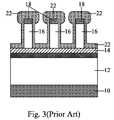
- FIGS. 1 through 3illustrate cross-sectional views of intermediate stages in a conventional process for achieving a below-lithograph-limitation pitch.
- silicon substrate 10is provided, which will be etched to form patterns, such as fins, in subsequent process steps.
- the formation of the finsrequires the help of the overlying layers that are used for lithography purposes.
- the overlying layersinclude a first ashing removable dielectric (ARD) 12 , silicon oxynitride 14 , a second ARD 16 , silicon oxynitride 18 , and photo resist 20 .
- Photo resist 20is patterned.
- spacer layer 22is formed using plasma enhanced chemical vapor deposition (PECVD).
- PECVDplasma enhanced chemical vapor deposition
- the thickness of the cap portions of spacer layer 22is significantly greater than the thickness of the sidewall portions of spacer layer 22 on the sidewalls of second ARD 16 .
- second ARD 16needs to be removed from between the sidewall portions of spacer layer 22 . Therefore, the increased thickness of the cap portions of spacer layer 22 adversely affects the subsequent process steps.
- deposition methods for forming conformal filmssuch as atomic layer deposition (ALD) cannot be used to solve the above-discussed problem. It has been found that when ALD is used to form spacer layer 22 , second ARD 16 as shown in FIG. 2 peels off. New methods are thus needed to solve the above-discussed problems.
- ALDatomic layer deposition
- a method of forming an integrated circuit structureincludes providing a substrate; forming a first hard mask layer over the substrate; forming a second hard mask layer over the first hard mask layer; patterning the second hard mask layer to form a hard mask; and after the step of patterning the second hard mask layer, baking the substrate, the first hard mask layer, and the hard mask. After the step of baking, a spacer layer is formed, which includes a first portion on a top of the hard mask, and a second portion and a third portion on opposite sidewalls of the hard mask.
- the methodfurther includes removing the first portion of the spacer layer; removing the hard mask, with the second portion and the third portion including remaining portions un-removed; and using the second portion and the third portion of the spacer layer as masks to pattern the first hard mask layer.
- a method of forming an integrated circuit structureincludes providing a semiconductor substrate; forming a first hard mask layer over the semiconductor substrate; forming an oxide layer over the first hard mask layer; forming a second hard mask layer over the oxide layer; patterning the second hard mask layer to form a first hard mask and a second hard mask close to each other; after the step of patterning the second hard mask layer, baking the substrate, the first hard mask layer, the first hard mask, and the second hard mask at a first temperature; and after the step of baking, forming a spacer layer at a second temperature no lower than the first temperature.
- the spacer layerincludes a first portion and a second portion on opposite sidewalls of the first hard mask, and a third portion and a fourth portion on opposite sidewalls of the second hard mask.
- the second portion and the third portionface each other and are spaced apart from each other.
- the methodfurther includes removing the first hard mask from between the first portion and the second portion of the spacer layer, and simultaneously removing the second hard mask from between the third portion and the fourth portion of the spacer layer; and using the first portion, the second portion, the third portion, and the fourth portion of the spacer layer as masks to pattern the first hard mask layer.
- a method of forming integrated circuit structuresincludes providing a substrate; forming a first hard mask layer over the substrate; forming an adhesion layer over and adjoining the first hard mask layer; forming an oxide layer over and adjoining the adhesion layer, wherein the oxide layer has a lower atomic percentage of silicon than the adhesion layer; forming a second hard mask layer over the oxide layer; patterning the second hard mask layer to form a hard mask; forming a spacer layer, wherein the spacer layer includes a first portion and a second portion on opposite sidewalls of the hard mask; removing the hard mask from between the first portion and the second portion of the spacer layer; and using the first portion and the second portion of the spacer layer as masks to pattern the first hard mask layer.
- the delamination problemis solved, and hence features with smaller pitches may be formed.
- FIGS. 1 through 3illustrate cross-sectional views of intermediate stages in a conventional process for achieving a below-lithograph-limitation pitch
- FIGS. 4 through 11illustrate cross-sectional views of intermediate stages in the manufacturing of an embodiment of the present invention.
- FIGS. 12 through 14illustrate cross-sectional views of intermediate stages in the manufacturing of an alternative embodiment of the present invention.
- FIG. 4illustrates a structure including substrate 30 and overlying layers.
- Substrate 30may be formed of a commonly used semiconductor material such as silicon, silicon germanium, or the like, and may be a bulk substrate or a semiconductor-on-insulator (SOI) substrate.
- Hard mask 32is formed over substrate 30 .
- hard mask 32comprises an ashing removable dielectric (ARD) material, and hence is referred to as ARD 32 hereinafter, although it may also be formed of other materials.
- ARD 32includes light-absorption layer 32 1 formed of, for example, amorphous silicon, and phase shift layer 32 2 , which has functions similar to that of an anti-reflective coating (ARC).
- ARCanti-reflective coating
- phase shift layer 32 2is also sometimes referred to as dielectric ARC, or DARC.
- ARD 32not only meets the selectivity requirement required for a hard mask layer, but also meets lithography-related requirements, such as the required reflectivity for the light used in the lithography steps. Further, ARD 32 can be removed by plasma ashing, and hence may be removed to form gaps having high aspect ratios.
- Plasma enhanced (PE) oxide 34which may be a silicon oxide formed using plasma enhanced chemical vapor deposition (PECVD), is formed over, and may adjoin, ARD 32 .
- Silicon oxynitride layer 36is formed over PE oxide 34 .
- PE oxide 34 and silicon oxynitride layer 36are both for lithographic purposes, for example, for reducing the reflection for the yellow light used in the exposure of the overlying photo resist. It is appreciated that layer 34 and/or layer 36 may also be formed of other materials.
- ARD 38silicon oxynitride layer 40 , and bottom anti-reflective coating (BARC) 42 are formed over silicon oxynitride layer 36 .
- ARD 38may be formed of the same materials, and may possibly have the same structure, as ARD 32 . Accordingly, ARD 38 may also include light absorption layer 38 1 , and phase shift layer 38 2 .
- layers 38 , 40 , and 42may be replaced by other materials and structures, and the number of layers may also be different from what is shown in FIG. 4 .
- Photo resist 44is formed over BARC 42 and patterned.
- layers 38 , 40 , 42 , and 44are used to form patterns with small pitches, which may be less than the minimum pitch allowed by the lithography process used for forming the integrated circuits, and layers 32 , 34 , and 36 are used to transfer the small pitches to substrate 30 .
- BARC 42 , silicon oxynitride layer 40 , and ARD 38are etched, for example, using plasma-assisted dry etching, followed by the removal of photo resist 44 and BARC 42 .
- the resulting structureis shown in FIG. 5 .
- ARD strips 46are thus formed. In the resulting structure, leftovers of silicon oxynitride layer 40 are likely to remain on top of ARD strips 46 .
- FIG. 6illustrates the baking of the structure shown in FIG. 5 , as is symbolized by arrows 48 .
- the baking temperatureneeds to be controlled carefully, in order to achieve the desired effect.
- the baking temperatureis preferably not too low, so that ARD 32 may outgas at a desirable rate.
- the baking temperatureis preferably not too high, so that the rate of outgassing from ARD 32 is not too high to cause an energy accumulation at the interface between ARD 32 and PE oxide 34 , which energy accumulation may cause delamination of PE oxide 34 from ARD 32 .
- the controlled temperaturethe outgas that would otherwise occur in the subsequent deposition of spacer layer 50 (refer to FIG.
- the temperature of the bakingis either equal to, or slightly lower than (for example, by less than about 10° C.), the temperature adopted by the deposition step as shown in FIG. 7 .
- the baking temperatureis between about 550° C. and about 900° C., and more preferably about 570° C.
- the baking durationmay be about 1 hour.
- the bakingis in-situ performed in the same chamber as the subsequent deposition step as shown in FIG. 7 , although it may also be performed in a different chamber or in a furnace.
- spacer layer 50is deposited using a conformal deposition method.
- spacer layer 50is deposited using atomic layer deposition (ALD), which may form a high quality film (with a low etching rate).
- ALDatomic layer deposition
- the conformitymay reach about 100 percent regardless of the surface condition.
- the ALDis performed between about 560° C. and about 900° C.
- Such high temperaturesare required for forming high-conformity films when the pitch P 1 is less than about 50 nm. However, such high temperatures also cause the outgassing of ARD 32 .
- the baking step performed before the deposition of spacer layer 50the likely delamination between ARD 32 and the overlying PE oxide 34 is eliminated due to the controlled outgassing and the gradual energy release.
- the ALDmay be performed using dichlorosilane (DCS) and ammonia as precursors, and the resulting spacer layer 50 may include silicon-rich nitride.
- DCSdichlorosilane
- LPCVDlow-pressure chemical vapor deposition
- the temperature of the LPCVDis between about 560° C. and about 900° C., although it may also be lower, for example, as low as about 300° C.
- the thickness T of spacer layer 50is preferably less than a half, and more preferably about a third, of pitch P 1 of ARD strips 46 .
- spacer layer 50is etched, for example, using dry etching, so that portions of spacer layer 50 directly over silicon oxynitride layer 36 are removed, and hence silicon oxynitride layer 36 is exposed. In addition, the cap portions of spacer layer 50 are removed, at least partially.
- the remaining portions of silicon oxynitride layer 40are removed, for example, using dry etch.
- ARD strips 46are then removed, for example, using plasma-assisted ashing.
- the resulting structureis shown in FIG. 9 .
- the remaining portions of spacer layer 50are used as masks for subsequent lithography processes, and are referred to as spacers 52 .
- the pitch P 2 of spacers 52is less than pitch P 1 .
- pitch P 2may be adjusted to about one-half of pitch P 1 . In the case pitch P 1 (which is also the pitch between ARD strips 46 ) is already close to the minimum pitch allowed by the existing lithography technology, pitch P 2 will be smaller than the minimum pitch.
- FIG. 10illustrates the transfer of the pattern of spacers 52 to ARD 32 , which involves various etching steps.
- ARD strips 56which are remaining portions of ARD 32 , are thus formed.
- ARD strips 56and possibly the overlying remaining patterns of spacers 52 are used as hard masks for etching substrate 30 .
- fins 58are formed.
- the remaining portions of ARD strips 56are removed, for example, by ashing, and the overlying materials, if any remain at this stage, are removed, leaving fins 58 .
- fins 58have a pitch smaller than pitch P 1 as shown in FIG. 7 , which may be the minimum pitch allowed by lithography technology.
- Fins 58may then be used to form FinFET transistors, for example, with a gate electrode of a FinFET (not shown) crossing more than one fin 58 . Accordingly, with the increased channel width as a result of multiple small fins, the drive current of the resulting FinFET is increased.
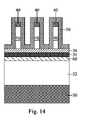
- FIGS. 12 through 14illustrate an alternative embodiment of the present invention.
- an initial structureis provided.
- the initial structureis similar to the structure as shown in FIG. 4 , except one or more adhesion layers 60 is inserted between ARD 32 and PE oxide 34 .
- Adhesion layer 60adjoins ARD 32 .
- Experiments performed by the inventors of the present inventionhave revealed that PE oxide 34 and ARD 32 have a poor adhesion, and hence are prone to the delamination caused by the build-up energy, which is the result of the degassing from ARD 32 .
- Adhesion layer 60has a solid bonding with ARD 32 , and also has a good adhesion with PE oxide 34 . Therefore, the delamination that otherwise would occur between layers 32 and 34 is eliminated.
- Adhesion layer 60preferably has good light reflection and absorption properties suitable for the lithography process.
- adhesion layer 60is formed of a silicon-rich material such as silicon oxynitride, silicon nitride, silicon-rich oxide, or combinations thereof, with the atomic percentage of silicon in the silicon-rich material being greater than the atomic percentage of silicon in layer 34 , which may be silicon oxide.
- Adhesion layer 60may also include multiple layers having good adhesion with both layers 32 and 34 .
- FIGS. 13 and 14illustrate the subsequent process steps.
- FIG. 13illustrates essentially a same step as shown in FIG. 5 .
- no bakingis performed between the steps of patterning ARD 38 and forming spacer layer 50 .
- a bakingis performed, which may be performed under essentially the same conditions as discussed in preceding paragraphs.
- spacer layer 50is formed.
- adhesion layer 60is formed instead of performing the baking, LPCVD is performed, which may be performed at a temperature between about 560° C. and about 900° C., although it may also be as low as about 300° C., or even lower.
- ALDmay be performed using essentially the same conditions as discussed in the preceding embodiment.
- the subsequent process stepsare essentially the same as shown in FIGS. 8 through 11 , and hence are not repeated herein.
- the delamination occurring between ARD 32 and overlying materialsis advantageously substantially eliminated.
- features with very small pitches and very small dimensionsmay be formed.
- the width W of fins 58 as shown in FIG. 11may be as small as about 10 nm.
Landscapes
- Engineering & Computer Science (AREA)
- Manufacturing & Machinery (AREA)
- Physics & Mathematics (AREA)
- Inorganic Chemistry (AREA)
- Condensed Matter Physics & Semiconductors (AREA)
- General Physics & Mathematics (AREA)
- Chemical & Material Sciences (AREA)
- Computer Hardware Design (AREA)
- Microelectronics & Electronic Packaging (AREA)
- Power Engineering (AREA)
- Internal Circuitry In Semiconductor Integrated Circuit Devices (AREA)
- Formation Of Insulating Films (AREA)
- Drying Of Semiconductors (AREA)
Abstract
Description
- This invention relates generally to integrated circuits, and more particularly to the fabrication of integrated circuits having pitches below lithograph resolution limits.
- The reduction in the scale of integrated circuits requires the reduction of lithograph resolution limits. Generally speaking, the minimum pitch of integrated circuits cannot be less than the lithograph resolution limit. However, there are exceptions. By adopting certain techniques, it is possible to reduce the pitch of integrated circuits below the lithograph resolution limit, although such techniques typically require more process steps.
FIGS. 1 through 3 illustrate cross-sectional views of intermediate stages in a conventional process for achieving a below-lithograph-limitation pitch. Referring toFIG. 1 ,silicon substrate 10 is provided, which will be etched to form patterns, such as fins, in subsequent process steps. The formation of the fins requires the help of the overlying layers that are used for lithography purposes. The overlying layers include a first ashing removable dielectric (ARD)12,silicon oxynitride 14, asecond ARD 16,silicon oxynitride 18, and photo resist20.Photo resist 20 is patterned.- Referring to
FIG. 2 , the patterns ofphoto resist 20 are transferred to theunderlying silicon oxynitride 18 and second ARD16 by dry etching. Typically,silicon oxynitride 18 will have remaining portions left over second ARD16. Next, as shown inFIG. 3 ,spacer layer 22 is formed using plasma enhanced chemical vapor deposition (PECVD). In technical generations with large pitches, for example, greater than about 50 nm,spacer layer 22 is relatively conformal. However, for integrated circuits formed using 50 nm technology and below, the method is no longer usable. The reason is that PECVD is sensitive to surface conditions. Theresulting spacer layer 22 is thus highly non-conformal, and for below 50 nm technologies, such non-conformity becomes too significant. It was noted that the thickness of the cap portions ofspacer layer 22 is significantly greater than the thickness of the sidewall portions ofspacer layer 22 on the sidewalls of second ARD16. In subsequent steps, second ARD16 needs to be removed from between the sidewall portions ofspacer layer 22. Therefore, the increased thickness of the cap portions ofspacer layer 22 adversely affects the subsequent process steps. - On the other hand, deposition methods for forming conformal films, such as atomic layer deposition (ALD), cannot be used to solve the above-discussed problem. It has been found that when ALD is used to form
spacer layer 22, second ARD16 as shown inFIG. 2 peels off. New methods are thus needed to solve the above-discussed problems. - In accordance with one aspect of the present invention, a method of forming an integrated circuit structure includes providing a substrate; forming a first hard mask layer over the substrate; forming a second hard mask layer over the first hard mask layer; patterning the second hard mask layer to form a hard mask; and after the step of patterning the second hard mask layer, baking the substrate, the first hard mask layer, and the hard mask. After the step of baking, a spacer layer is formed, which includes a first portion on a top of the hard mask, and a second portion and a third portion on opposite sidewalls of the hard mask. The method further includes removing the first portion of the spacer layer; removing the hard mask, with the second portion and the third portion including remaining portions un-removed; and using the second portion and the third portion of the spacer layer as masks to pattern the first hard mask layer.
- In accordance with another aspect of the present invention, a method of forming an integrated circuit structure includes providing a semiconductor substrate; forming a first hard mask layer over the semiconductor substrate; forming an oxide layer over the first hard mask layer; forming a second hard mask layer over the oxide layer; patterning the second hard mask layer to form a first hard mask and a second hard mask close to each other; after the step of patterning the second hard mask layer, baking the substrate, the first hard mask layer, the first hard mask, and the second hard mask at a first temperature; and after the step of baking, forming a spacer layer at a second temperature no lower than the first temperature. The spacer layer includes a first portion and a second portion on opposite sidewalls of the first hard mask, and a third portion and a fourth portion on opposite sidewalls of the second hard mask. The second portion and the third portion face each other and are spaced apart from each other. The method further includes removing the first hard mask from between the first portion and the second portion of the spacer layer, and simultaneously removing the second hard mask from between the third portion and the fourth portion of the spacer layer; and using the first portion, the second portion, the third portion, and the fourth portion of the spacer layer as masks to pattern the first hard mask layer.
- In accordance with yet another aspect of the present invention, a method of forming integrated circuit structures includes providing a substrate; forming a first hard mask layer over the substrate; forming an adhesion layer over and adjoining the first hard mask layer; forming an oxide layer over and adjoining the adhesion layer, wherein the oxide layer has a lower atomic percentage of silicon than the adhesion layer; forming a second hard mask layer over the oxide layer; patterning the second hard mask layer to form a hard mask; forming a spacer layer, wherein the spacer layer includes a first portion and a second portion on opposite sidewalls of the hard mask; removing the hard mask from between the first portion and the second portion of the spacer layer; and using the first portion and the second portion of the spacer layer as masks to pattern the first hard mask layer.
- By performing the embodiments of the present invention, the delamination problem is solved, and hence features with smaller pitches may be formed.
- For a more complete understanding of the present invention, and the advantages thereof, reference is now made to the following descriptions taken in conjunction with the accompanying drawings, in which:
FIGS. 1 through 3 illustrate cross-sectional views of intermediate stages in a conventional process for achieving a below-lithograph-limitation pitch;FIGS. 4 through 11 illustrate cross-sectional views of intermediate stages in the manufacturing of an embodiment of the present invention; andFIGS. 12 through 14 illustrate cross-sectional views of intermediate stages in the manufacturing of an alternative embodiment of the present invention.- The making and using of the presently preferred embodiments are discussed in detail below. It should be appreciated, however, that the present invention provides many applicable inventive concepts that can be embodied in a wide variety of specific contexts. The specific embodiments discussed are merely illustrative of specific ways to make and use the invention, and do not limit the scope of the invention.
- A novel method for forming below-lithograph-limit patterns in integrated circuits is provided. The intermediate stages of manufacturing preferred embodiments of the present invention are illustrated. Variations of the preferred embodiments are then discussed. Throughout the various views and illustrative embodiments of the present invention, like reference numbers are used to designate like elements.
FIG. 4 illustrates astructure including substrate 30 and overlying layers.Substrate 30 may be formed of a commonly used semiconductor material such as silicon, silicon germanium, or the like, and may be a bulk substrate or a semiconductor-on-insulator (SOI) substrate.Hard mask 32 is formed oversubstrate 30. Preferably,hard mask 32 comprises an ashing removable dielectric (ARD) material, and hence is referred to as ARD32 hereinafter, although it may also be formed of other materials. In an embodiment, ARD32 includes light-absorption layer 321formed of, for example, amorphous silicon, andphase shift layer 322, which has functions similar to that of an anti-reflective coating (ARC). Accordingly,phase shift layer 322is also sometimes referred to as dielectric ARC, or DARC. Advantageously, ARD32 not only meets the selectivity requirement required for a hard mask layer, but also meets lithography-related requirements, such as the required reflectivity for the light used in the lithography steps. Further, ARD32 can be removed by plasma ashing, and hence may be removed to form gaps having high aspect ratios.- Plasma enhanced (PE)
oxide 34, which may be a silicon oxide formed using plasma enhanced chemical vapor deposition (PECVD), is formed over, and may adjoin, ARD32.Silicon oxynitride layer 36 is formed overPE oxide 34.PE oxide 34 andsilicon oxynitride layer 36 are both for lithographic purposes, for example, for reducing the reflection for the yellow light used in the exposure of the overlying photo resist. It is appreciated thatlayer 34 and/orlayer 36 may also be formed of other materials. - ARD38,
silicon oxynitride layer 40, and bottom anti-reflective coating (BARC)42 are formed oversilicon oxynitride layer 36. ARD38 may be formed of the same materials, and may possibly have the same structure, as ARD32. Accordingly, ARD38 may also includelight absorption layer 381, andphase shift layer 382. One skilled in the art will realize thatlayers FIG. 4 .Photo resist 44 is formed over BARC42 and patterned. Preferably, as will be discussed in detail in subsequent paragraphs, layers38,40,42, and44 are used to form patterns with small pitches, which may be less than the minimum pitch allowed by the lithography process used for forming the integrated circuits, and layers32,34, and36 are used to transfer the small pitches tosubstrate 30. - Next,
BARC 42,silicon oxynitride layer 40, andARD 38 are etched, for example, using plasma-assisted dry etching, followed by the removal of photo resist44 andBARC 42. The resulting structure is shown inFIG. 5 . ARD strips46 are thus formed. In the resulting structure, leftovers ofsilicon oxynitride layer 40 are likely to remain on top of ARD strips46. FIG. 6 illustrates the baking of the structure shown inFIG. 5 , as is symbolized byarrows 48. The baking temperature needs to be controlled carefully, in order to achieve the desired effect. The baking temperature is preferably not too low, so thatARD 32 may outgas at a desirable rate. On the other hand, the baking temperature is preferably not too high, so that the rate of outgassing fromARD 32 is not too high to cause an energy accumulation at the interface betweenARD 32 andPE oxide 34, which energy accumulation may cause delamination ofPE oxide 34 fromARD 32. With the controlled temperature, the outgas that would otherwise occur in the subsequent deposition of spacer layer50 (refer toFIG. 7 ) occurs in the baking step in a controlled manner, and hence the energy that would otherwise accumulate rapidly in the subsequent deposition is released gradually. It is thus desirable that the temperature of the baking is either equal to, or slightly lower than (for example, by less than about 10° C.), the temperature adopted by the deposition step as shown inFIG. 7 . In an exemplary embodiment, the baking temperature is between about 550° C. and about 900° C., and more preferably about 570° C. The baking duration may be about 1 hour. In the preferred embodiment, the baking is in-situ performed in the same chamber as the subsequent deposition step as shown inFIG. 7 , although it may also be performed in a different chamber or in a furnace.- Next, as shown in
FIG. 7 ,spacer layer 50 is deposited using a conformal deposition method. In the preferred embodiment,spacer layer 50 is deposited using atomic layer deposition (ALD), which may form a high quality film (with a low etching rate). The conformity may reach about 100 percent regardless of the surface condition. In an exemplary embodiment, the ALD is performed between about 560° C. and about 900° C. Such high temperatures are required for forming high-conformity films when the pitch P1 is less than about 50 nm. However, such high temperatures also cause the outgassing ofARD 32. Advantageously, with the baking step performed before the deposition ofspacer layer 50, the likely delamination betweenARD 32 and theoverlying PE oxide 34 is eliminated due to the controlled outgassing and the gradual energy release. The ALD may be performed using dichlorosilane (DCS) and ammonia as precursors, and the resultingspacer layer 50 may include silicon-rich nitride. In alternative embodiments, other conformal deposition methods, such as low-pressure chemical vapor deposition (LPCVD), may be performed. In an exemplary embodiment, the temperature of the LPCVD is between about 560° C. and about 900° C., although it may also be lower, for example, as low as about 300° C. The thickness T ofspacer layer 50 is preferably less than a half, and more preferably about a third, of pitch P1 of ARD strips46. - In
FIG. 8 ,spacer layer 50 is etched, for example, using dry etching, so that portions ofspacer layer 50 directly oversilicon oxynitride layer 36 are removed, and hencesilicon oxynitride layer 36 is exposed. In addition, the cap portions ofspacer layer 50 are removed, at least partially. - Next, the remaining portions of
silicon oxynitride layer 40 are removed, for example, using dry etch. ARD strips46 are then removed, for example, using plasma-assisted ashing. The resulting structure is shown inFIG. 9 . The remaining portions ofspacer layer 50 are used as masks for subsequent lithography processes, and are referred to asspacers 52. It is noted that the pitch P2 ofspacers 52 is less than pitch P1. By adjusting the thickness T1 of spacer layers50 and the thickness T2 of ARD strips46, pitch P2 may be adjusted to about one-half of pitch P1. In the case pitch P1 (which is also the pitch between ARD strips46) is already close to the minimum pitch allowed by the existing lithography technology, pitch P2 will be smaller than the minimum pitch. FIG. 10 illustrates the transfer of the pattern ofspacers 52 toARD 32, which involves various etching steps. ARD strips56, which are remaining portions ofARD 32, are thus formed. Next, as shown inFIG. 11 , ARD strips56, and possibly the overlying remaining patterns ofspacers 52 are used as hard masks for etchingsubstrate 30. As a result,fins 58 are formed. Next, the remaining portions of ARD strips56 are removed, for example, by ashing, and the overlying materials, if any remain at this stage, are removed, leavingfins 58. Advantageously,fins 58 have a pitch smaller than pitch P1 as shown inFIG. 7 , which may be the minimum pitch allowed by lithography technology.Fins 58 may then be used to form FinFET transistors, for example, with a gate electrode of a FinFET (not shown) crossing more than onefin 58. Accordingly, with the increased channel width as a result of multiple small fins, the drive current of the resulting FinFET is increased.FIGS. 12 through 14 illustrate an alternative embodiment of the present invention. Referring toFIG. 12 , an initial structure is provided. The initial structure is similar to the structure as shown inFIG. 4 , except one or more adhesion layers60 is inserted betweenARD 32 andPE oxide 34.Adhesion layer 60 adjoinsARD 32. Experiments performed by the inventors of the present invention have revealed thatPE oxide 34 andARD 32 have a poor adhesion, and hence are prone to the delamination caused by the build-up energy, which is the result of the degassing fromARD 32.Adhesion layer 60 has a solid bonding withARD 32, and also has a good adhesion withPE oxide 34. Therefore, the delamination that otherwise would occur betweenlayers Adhesion layer 60 preferably has good light reflection and absorption properties suitable for the lithography process. In the preferred embodiment,adhesion layer 60 is formed of a silicon-rich material such as silicon oxynitride, silicon nitride, silicon-rich oxide, or combinations thereof, with the atomic percentage of silicon in the silicon-rich material being greater than the atomic percentage of silicon inlayer 34, which may be silicon oxide.Adhesion layer 60 may also include multiple layers having good adhesion with bothlayers FIGS. 13 and 14 illustrate the subsequent process steps.FIG. 13 illustrates essentially a same step as shown inFIG. 5 . In an embodiment, no baking is performed between the steps ofpatterning ARD 38 and formingspacer layer 50. In alternative embodiments, a baking is performed, which may be performed under essentially the same conditions as discussed in preceding paragraphs. InFIG. 14 ,spacer layer 50 is formed. Preferably, in thecase adhesion layer 60 is formed instead of performing the baking, LPCVD is performed, which may be performed at a temperature between about 560° C. and about 900° C., although it may also be as low as about 300° C., or even lower. Alternatively, ALD may be performed using essentially the same conditions as discussed in the preceding embodiment. The subsequent process steps are essentially the same as shown inFIGS. 8 through 11 , and hence are not repeated herein.- It is noted that although the embodiments discussed in the preceding paragraphs provide the formation process steps of semiconductor fins, the same method may also be used to form other small-pitch features other than semiconductor fins, wherein the small pitches may be smaller than the minimum pitch allowed by the respective lithography process.
- In the embodiments of the present invention, the delamination occurring between
ARD 32 and overlying materials is advantageously substantially eliminated. As a result, features with very small pitches and very small dimensions may be formed. For example, in the case the minimum pitch allowed by the respective lithography process is about 28 nm, the width W offins 58 as shown inFIG. 11 may be as small as about 10 nm. - Although the present invention and its advantages have been described in detail, it should be understood that various changes, substitutions and alterations can be made herein without departing from the spirit and scope of the invention as defined by the appended claims. Moreover, the scope of the present application is not intended to be limited to the particular embodiments of the process, machine, manufacture, and composition of matter, means, methods and steps described in the specification. As one of ordinary skill in the art will readily appreciate from the disclosure of the present invention, processes, machines, manufacture, compositions of matter, means, methods, or steps, presently existing or later to be developed, that perform substantially the same function or achieve substantially the same result as the corresponding embodiments described herein may be utilized according to the present invention. Accordingly, the appended claims are intended to include within their scope such processes, machines, manufacture, compositions of matter, means, methods, or steps.
Claims (20)
Priority Applications (3)
| Application Number | Priority Date | Filing Date | Title |
|---|---|---|---|
| US12/326,099US8048813B2 (en) | 2008-12-01 | 2008-12-01 | Method of reducing delamination in the fabrication of small-pitch devices |
| CN200910136625XACN101752303B (en) | 2008-12-01 | 2009-05-08 | Method of reducing delamination in the fabrication of small-pitch devices |
| US13/253,694US8778807B2 (en) | 2008-12-01 | 2011-10-05 | Method of reducing delamination in the fabrication of small-pitch devices |
Applications Claiming Priority (1)
| Application Number | Priority Date | Filing Date | Title |
|---|---|---|---|
| US12/326,099US8048813B2 (en) | 2008-12-01 | 2008-12-01 | Method of reducing delamination in the fabrication of small-pitch devices |
Related Child Applications (1)
| Application Number | Title | Priority Date | Filing Date |
|---|---|---|---|
| US13/253,694DivisionUS8778807B2 (en) | 2008-12-01 | 2011-10-05 | Method of reducing delamination in the fabrication of small-pitch devices |
Publications (2)
| Publication Number | Publication Date |
|---|---|
| US20100136791A1true US20100136791A1 (en) | 2010-06-03 |
| US8048813B2 US8048813B2 (en) | 2011-11-01 |
Family
ID=42223207
Family Applications (2)
| Application Number | Title | Priority Date | Filing Date |
|---|---|---|---|
| US12/326,099Expired - Fee RelatedUS8048813B2 (en) | 2008-12-01 | 2008-12-01 | Method of reducing delamination in the fabrication of small-pitch devices |
| US13/253,694Active2028-12-15US8778807B2 (en) | 2008-12-01 | 2011-10-05 | Method of reducing delamination in the fabrication of small-pitch devices |
Family Applications After (1)
| Application Number | Title | Priority Date | Filing Date |
|---|---|---|---|
| US13/253,694Active2028-12-15US8778807B2 (en) | 2008-12-01 | 2011-10-05 | Method of reducing delamination in the fabrication of small-pitch devices |
Country Status (2)
| Country | Link |
|---|---|
| US (2) | US8048813B2 (en) |
| CN (1) | CN101752303B (en) |
Cited By (7)
| Publication number | Priority date | Publication date | Assignee | Title |
|---|---|---|---|---|
| WO2012128843A3 (en)* | 2011-03-23 | 2013-03-14 | International Business Machines Corporation | Improved sidewall image transfer process |
| US20150061087A1 (en)* | 2013-09-04 | 2015-03-05 | Semiconductor Manufacturing International (Shanghai) Corporation | Triple patterning method |
| US20150115365A1 (en)* | 2012-06-14 | 2015-04-30 | International Business Machines Corporation | Continuously scalable width and height semiconductor fins |
| US20150325441A1 (en)* | 2014-05-09 | 2015-11-12 | Powerchip Technology Corporation | Semiconductor fabrication method |
| US9536744B1 (en)* | 2015-12-17 | 2017-01-03 | International Business Machines Corporation | Enabling large feature alignment marks with sidewall image transfer patterning |
| TWI621210B (en)* | 2014-08-27 | 2018-04-11 | 聯華電子股份有限公司 | Method for fabricating semiconductor device |
| US10672612B2 (en) | 2018-04-04 | 2020-06-02 | United Microelectronics Corp. | Method of forming semiconductor structure |
Families Citing this family (11)
| Publication number | Priority date | Publication date | Assignee | Title |
|---|---|---|---|---|
| CN102386059B (en)* | 2010-09-03 | 2013-06-12 | 中芯国际集成电路制造(上海)有限公司 | Method for forming small-spacing pattern |
| US8629040B2 (en)* | 2011-11-16 | 2014-01-14 | Taiwan Semiconductor Manufacturing Company, Ltd. | Methods for epitaxially growing active regions between STI regions |
| US8822284B2 (en) | 2012-02-09 | 2014-09-02 | United Microelectronics Corp. | Method for fabricating FinFETs and semiconductor structure fabricated using the method |
| US9059254B2 (en) | 2012-09-06 | 2015-06-16 | International Business Machines Corporation | Overlay-tolerant via mask and reactive ion etch (RIE) technique |
| US8501607B1 (en)* | 2012-11-07 | 2013-08-06 | Globalfoundries Inc. | FinFET alignment structures using a double trench flow |
| US8828839B2 (en)* | 2013-01-29 | 2014-09-09 | GlobalFoundries, Inc. | Methods for fabricating electrically-isolated finFET semiconductor devices |
| US8993218B2 (en)* | 2013-02-20 | 2015-03-31 | Taiwan Semiconductor Manufacturing Company Limited | Photo resist (PR) profile control |
| US9177797B2 (en)* | 2013-12-04 | 2015-11-03 | Taiwan Semiconductor Manufacturing Company, Ltd. | Lithography using high selectivity spacers for pitch reduction |
| US9685507B2 (en) | 2015-06-25 | 2017-06-20 | International Business Machines Corporation | FinFET devices |
| US9899378B2 (en) | 2015-12-14 | 2018-02-20 | International Business Machines Corporation | Simultaneously fabricating a high voltage transistor and a finFET |
| US9882028B2 (en)* | 2016-06-29 | 2018-01-30 | International Business Machines Corporation | Pitch split patterning for semiconductor devices |
Citations (17)
| Publication number | Priority date | Publication date | Assignee | Title |
|---|---|---|---|---|
| US5047117A (en)* | 1990-09-26 | 1991-09-10 | Micron Technology, Inc. | Method of forming a narrow self-aligned, annular opening in a masking layer |
| US6706571B1 (en)* | 2002-10-22 | 2004-03-16 | Advanced Micro Devices, Inc. | Method for forming multiple structures in a semiconductor device |
| US20040253388A1 (en)* | 2003-06-16 | 2004-12-16 | Tae Kyung Kim | Method for forming low dielectric layer of semiconductor device |
| US6858478B2 (en)* | 2002-08-23 | 2005-02-22 | Intel Corporation | Tri-gate devices and methods of fabrication |
| US20050153490A1 (en)* | 2003-12-16 | 2005-07-14 | Jae-Man Yoon | Method of forming fin field effect transistor |
| US7190050B2 (en)* | 2005-07-01 | 2007-03-13 | Synopsys, Inc. | Integrated circuit on corrugated substrate |
| US20070122953A1 (en)* | 2005-07-01 | 2007-05-31 | Synopsys, Inc. | Enhanced Segmented Channel MOS Transistor with High-Permittivity Dielectric Isolation Material |
| US20070122954A1 (en)* | 2005-07-01 | 2007-05-31 | Synopsys, Inc. | Sequential Selective Epitaxial Growth |
| US20070120156A1 (en)* | 2005-07-01 | 2007-05-31 | Synopsys, Inc. | Enhanced Segmented Channel MOS Transistor with Multi Layer Regions |
| US20070128782A1 (en)* | 2005-07-01 | 2007-06-07 | Synopsys, Inc. | Enhanced Segmented Channel MOS Transistor with Narrowed Base Regions |
| US20070161251A1 (en)* | 2005-03-15 | 2007-07-12 | Micron Technology, Inc. | Pitch reduced patterns relative to photolithography features |
| US7247887B2 (en)* | 2005-07-01 | 2007-07-24 | Synopsys, Inc. | Segmented channel MOS transistor |
| US7265008B2 (en)* | 2005-07-01 | 2007-09-04 | Synopsys, Inc. | Method of IC production using corrugated substrate |
| US20080296632A1 (en)* | 2007-05-30 | 2008-12-04 | Synopsys, Inc. | Stress-Enhanced Performance Of A FinFet Using Surface/Channel Orientations And Strained Capping Layers |
| US20090142926A1 (en)* | 2007-06-04 | 2009-06-04 | Huixiong Dai | Line edge roughness reduction and double patterning |
| US7611980B2 (en)* | 2006-08-30 | 2009-11-03 | Micron Technology, Inc. | Single spacer process for multiplying pitch by a factor greater than two and related intermediate IC structures |
| US7795149B2 (en)* | 2006-06-01 | 2010-09-14 | Micron Technology, Inc. | Masking techniques and contact imprint reticles for dense semiconductor fabrication |
Family Cites Families (17)
| Publication number | Priority date | Publication date | Assignee | Title |
|---|---|---|---|---|
| US5328810A (en)* | 1990-05-07 | 1994-07-12 | Micron Technology, Inc. | Method for reducing, by a factor or 2-N, the minimum masking pitch of a photolithographic process |
| US5741626A (en)* | 1996-04-15 | 1998-04-21 | Motorola, Inc. | Method for forming a dielectric tantalum nitride layer as an anti-reflective coating (ARC) |
| US6432827B1 (en)* | 2000-11-29 | 2002-08-13 | United Microelectronics Corp. | ILD planarization method |
| US6429106B1 (en)* | 2001-01-19 | 2002-08-06 | United Microelectronics Corp. | Method of automatically defining a landing via |
| US6762130B2 (en)* | 2002-05-31 | 2004-07-13 | Texas Instruments Incorporated | Method of photolithographically forming extremely narrow transistor gate elements |
| DE10260619B4 (en)* | 2002-12-23 | 2011-02-24 | Globalfoundries Inc. | Process for producing a cover layer with antireflective properties on a low-k dielectric |
| US7015136B2 (en)* | 2003-07-10 | 2006-03-21 | Taiwan Semiconductor Manufacturing Co., Ltd. | Method for preventing formation of photoresist scum |
| US7390746B2 (en)* | 2005-03-15 | 2008-06-24 | Micron Technology, Inc. | Multiple deposition for integration of spacers in pitch multiplication process |
| US7560390B2 (en)* | 2005-06-02 | 2009-07-14 | Micron Technology, Inc. | Multiple spacer steps for pitch multiplication |
| KR100703985B1 (en)* | 2006-02-17 | 2007-04-09 | 삼성전자주식회사 | Manufacturing Method of Semiconductor Device |
| KR100822581B1 (en)* | 2006-09-08 | 2008-04-16 | 주식회사 하이닉스반도체 | Manufacturing Method of Flash Memory Device |
| KR100855845B1 (en)* | 2006-09-12 | 2008-09-01 | 주식회사 하이닉스반도체 | Method for Forming Fine Patterns of Semiconductor Devices |
| KR100790998B1 (en)* | 2006-10-02 | 2008-01-03 | 삼성전자주식회사 | Pad pattern formation method using self-aligned double patterning method and contact hole formation method using self-aligned double patterning method |
| US20080272361A1 (en)* | 2007-05-02 | 2008-11-06 | Atomate Corporation | High Density Nanotube Devices |
| KR100942078B1 (en)* | 2007-12-27 | 2010-02-12 | 주식회사 하이닉스반도체 | Method of forming fine pattern of semiconductor device |
| KR100933854B1 (en)* | 2008-01-14 | 2009-12-24 | 주식회사 하이닉스반도체 | Pattern formation method of semiconductor device |
| US7601641B1 (en)* | 2008-03-31 | 2009-10-13 | Global Foundries, Inc. | Two step optical planarizing layer etch |
- 2008
- 2008-12-01USUS12/326,099patent/US8048813B2/ennot_activeExpired - Fee Related
- 2009
- 2009-05-08CNCN200910136625XApatent/CN101752303B/ennot_activeExpired - Fee Related
- 2011
- 2011-10-05USUS13/253,694patent/US8778807B2/enactiveActive
Patent Citations (23)
| Publication number | Priority date | Publication date | Assignee | Title |
|---|---|---|---|---|
| US5047117A (en)* | 1990-09-26 | 1991-09-10 | Micron Technology, Inc. | Method of forming a narrow self-aligned, annular opening in a masking layer |
| US6858478B2 (en)* | 2002-08-23 | 2005-02-22 | Intel Corporation | Tri-gate devices and methods of fabrication |
| US6706571B1 (en)* | 2002-10-22 | 2004-03-16 | Advanced Micro Devices, Inc. | Method for forming multiple structures in a semiconductor device |
| US20040253388A1 (en)* | 2003-06-16 | 2004-12-16 | Tae Kyung Kim | Method for forming low dielectric layer of semiconductor device |
| US20050153490A1 (en)* | 2003-12-16 | 2005-07-14 | Jae-Man Yoon | Method of forming fin field effect transistor |
| US20070161251A1 (en)* | 2005-03-15 | 2007-07-12 | Micron Technology, Inc. | Pitch reduced patterns relative to photolithography features |
| US20070132053A1 (en)* | 2005-07-01 | 2007-06-14 | Synopsys Inc. | Integrated Circuit On Corrugated Substrate |
| US20090181477A1 (en)* | 2005-07-01 | 2009-07-16 | Synopsys, Inc. | Integrated Circuit On Corrugated Substrate |
| US20070120156A1 (en)* | 2005-07-01 | 2007-05-31 | Synopsys, Inc. | Enhanced Segmented Channel MOS Transistor with Multi Layer Regions |
| US20070128782A1 (en)* | 2005-07-01 | 2007-06-07 | Synopsys, Inc. | Enhanced Segmented Channel MOS Transistor with Narrowed Base Regions |
| US20070122953A1 (en)* | 2005-07-01 | 2007-05-31 | Synopsys, Inc. | Enhanced Segmented Channel MOS Transistor with High-Permittivity Dielectric Isolation Material |
| US7190050B2 (en)* | 2005-07-01 | 2007-03-13 | Synopsys, Inc. | Integrated circuit on corrugated substrate |
| US7247887B2 (en)* | 2005-07-01 | 2007-07-24 | Synopsys, Inc. | Segmented channel MOS transistor |
| US7265008B2 (en)* | 2005-07-01 | 2007-09-04 | Synopsys, Inc. | Method of IC production using corrugated substrate |
| US20080290470A1 (en)* | 2005-07-01 | 2008-11-27 | Synopsys, Inc. | Integrated Circuit On Corrugated Substrate |
| US7605449B2 (en)* | 2005-07-01 | 2009-10-20 | Synopsys, Inc. | Enhanced segmented channel MOS transistor with high-permittivity dielectric isolation material |
| US7508031B2 (en)* | 2005-07-01 | 2009-03-24 | Synopsys, Inc. | Enhanced segmented channel MOS transistor with narrowed base regions |
| US7528465B2 (en)* | 2005-07-01 | 2009-05-05 | Synopsys, Inc. | Integrated circuit on corrugated substrate |
| US20070122954A1 (en)* | 2005-07-01 | 2007-05-31 | Synopsys, Inc. | Sequential Selective Epitaxial Growth |
| US7795149B2 (en)* | 2006-06-01 | 2010-09-14 | Micron Technology, Inc. | Masking techniques and contact imprint reticles for dense semiconductor fabrication |
| US7611980B2 (en)* | 2006-08-30 | 2009-11-03 | Micron Technology, Inc. | Single spacer process for multiplying pitch by a factor greater than two and related intermediate IC structures |
| US20080296632A1 (en)* | 2007-05-30 | 2008-12-04 | Synopsys, Inc. | Stress-Enhanced Performance Of A FinFet Using Surface/Channel Orientations And Strained Capping Layers |
| US20090142926A1 (en)* | 2007-06-04 | 2009-06-04 | Huixiong Dai | Line edge roughness reduction and double patterning |
Cited By (10)
| Publication number | Priority date | Publication date | Assignee | Title |
|---|---|---|---|---|
| WO2012128843A3 (en)* | 2011-03-23 | 2013-03-14 | International Business Machines Corporation | Improved sidewall image transfer process |
| US8883649B2 (en) | 2011-03-23 | 2014-11-11 | International Business Machines Corporation | Sidewall image transfer process |
| US20150115365A1 (en)* | 2012-06-14 | 2015-04-30 | International Business Machines Corporation | Continuously scalable width and height semiconductor fins |
| US20150061087A1 (en)* | 2013-09-04 | 2015-03-05 | Semiconductor Manufacturing International (Shanghai) Corporation | Triple patterning method |
| US9034762B2 (en)* | 2013-09-04 | 2015-05-19 | Semiconductor Manufacturing International (Shanghai) Corporation | Triple patterning method |
| US20150325441A1 (en)* | 2014-05-09 | 2015-11-12 | Powerchip Technology Corporation | Semiconductor fabrication method |
| TWI621210B (en)* | 2014-08-27 | 2018-04-11 | 聯華電子股份有限公司 | Method for fabricating semiconductor device |
| US9536744B1 (en)* | 2015-12-17 | 2017-01-03 | International Business Machines Corporation | Enabling large feature alignment marks with sidewall image transfer patterning |
| US9716184B2 (en)* | 2015-12-17 | 2017-07-25 | International Business Machines Corporation | Enabling large feature alignment marks with sidewall image transfer patterning |
| US10672612B2 (en) | 2018-04-04 | 2020-06-02 | United Microelectronics Corp. | Method of forming semiconductor structure |
Also Published As
| Publication number | Publication date |
|---|---|
| US20120028473A1 (en) | 2012-02-02 |
| CN101752303B (en) | 2012-04-25 |
| US8778807B2 (en) | 2014-07-15 |
| US8048813B2 (en) | 2011-11-01 |
| CN101752303A (en) | 2010-06-23 |
Similar Documents
| Publication | Publication Date | Title |
|---|---|---|
| US8048813B2 (en) | Method of reducing delamination in the fabrication of small-pitch devices | |
| US10049878B2 (en) | Self-aligned patterning process | |
| CN100472714C (en) | Method for making hard mask | |
| JP6133585B2 (en) | EUV photoresist encapsulation | |
| US9129906B2 (en) | Self-aligned double spacer patterning process | |
| US8728945B2 (en) | Method for patterning sublithographic features | |
| US20090258500A1 (en) | Method of forming a pattern for a semiconductor device and method of forming the related mos transistor | |
| US20130217233A1 (en) | Methods for Controlling Line Dimensions in Spacer Alignment Double Patterning Semiconductor Processing | |
| US20130122686A1 (en) | Reverse Tone STI Formation | |
| US8951918B2 (en) | Method for fabricating patterned structure of semiconductor device | |
| US20090004862A1 (en) | Method for forming fine patterns in semiconductor device | |
| US20090170330A1 (en) | Method of forming a micro pattern of a semiconductor device | |
| JP2008258565A (en) | Method of forming micro pattern of semiconductor device | |
| KR20090027429A (en) | Method of forming fine pattern of semiconductor device | |
| JP2009071306A (en) | Method for forming micropattern in semiconductor device | |
| US9570304B2 (en) | Method of forming fine patterns in an anti-reflection layer for use as a patterning hard mask | |
| TWI567785B (en) | Method for fabricating patterned structure of semiconductor device | |
| US20090170310A1 (en) | Method of forming a metal line of a semiconductor device | |
| US9513542B2 (en) | Lithography mask and method of forming a lithography mask | |
| US8524608B1 (en) | Method for fabricating a patterned structure of a semiconductor device | |
| KR100798738B1 (en) | Manufacturing method of fine pattern of semiconductor device | |
| US20180323072A1 (en) | Method For Increasing Trench CD in EUV Patterning Without Increasing Single Line Opens or Roughness | |
| KR20090001080A (en) | Method of forming fine pattern of semiconductor device | |
| KR20050047300A (en) | Pattern formation method using silicon protective layer for improving an etching selectivity of a photoresist film in a semiconductor device | |
| KR100728993B1 (en) | Manufacturing method of semiconductor device |
Legal Events
| Date | Code | Title | Description |
|---|---|---|---|
| AS | Assignment | Owner name:TAIWAN SEMICONDUCTOR MANUFACTURING COMPANY, LTD.,T Free format text:ASSIGNMENT OF ASSIGNORS INTEREST;ASSIGNORS:LAI, CHIH-YU;WU, CHENG-TA;CHEN, NENG-KUO;AND OTHERS;REEL/FRAME:021915/0427 Effective date:20081124 Owner name:TAIWAN SEMICONDUCTOR MANUFACTURING COMPANY, LTD., Free format text:ASSIGNMENT OF ASSIGNORS INTEREST;ASSIGNORS:LAI, CHIH-YU;WU, CHENG-TA;CHEN, NENG-KUO;AND OTHERS;REEL/FRAME:021915/0427 Effective date:20081124 | |
| ZAAA | Notice of allowance and fees due | Free format text:ORIGINAL CODE: NOA | |
| ZAAB | Notice of allowance mailed | Free format text:ORIGINAL CODE: MN/=. | |
| STCF | Information on status: patent grant | Free format text:PATENTED CASE | |
| FPAY | Fee payment | Year of fee payment:4 | |
| MAFP | Maintenance fee payment | Free format text:PAYMENT OF MAINTENANCE FEE, 8TH YEAR, LARGE ENTITY (ORIGINAL EVENT CODE: M1552); ENTITY STATUS OF PATENT OWNER: LARGE ENTITY Year of fee payment:8 | |
| FEPP | Fee payment procedure | Free format text:MAINTENANCE FEE REMINDER MAILED (ORIGINAL EVENT CODE: REM.); ENTITY STATUS OF PATENT OWNER: LARGE ENTITY | |
| LAPS | Lapse for failure to pay maintenance fees | Free format text:PATENT EXPIRED FOR FAILURE TO PAY MAINTENANCE FEES (ORIGINAL EVENT CODE: EXP.); ENTITY STATUS OF PATENT OWNER: LARGE ENTITY | |
| STCH | Information on status: patent discontinuation | Free format text:PATENT EXPIRED DUE TO NONPAYMENT OF MAINTENANCE FEES UNDER 37 CFR 1.362 | |
| FP | Lapsed due to failure to pay maintenance fee | Effective date:20231101 |