US20100136262A1 - Inductive plasma source with high coupling efficiency - Google Patents
Inductive plasma source with high coupling efficiencyDownload PDFInfo
- Publication number
- US20100136262A1 US20100136262A1US12/471,375US47137509AUS2010136262A1US 20100136262 A1US20100136262 A1US 20100136262A1US 47137509 AUS47137509 AUS 47137509AUS 2010136262 A1US2010136262 A1US 2010136262A1
- Authority
- US
- United States
- Prior art keywords
- chamber
- window
- plasma
- inductive coupling
- applicator
- Prior art date
- Legal status (The legal status is an assumption and is not a legal conclusion. Google has not performed a legal analysis and makes no representation as to the accuracy of the status listed.)
- Granted
Links
Images


Classifications
- H—ELECTRICITY
- H01—ELECTRIC ELEMENTS
- H01J—ELECTRIC DISCHARGE TUBES OR DISCHARGE LAMPS
- H01J37/00—Discharge tubes with provision for introducing objects or material to be exposed to the discharge, e.g. for the purpose of examination or processing thereof
- H01J37/32—Gas-filled discharge tubes
- H01J37/32009—Arrangements for generation of plasma specially adapted for examination or treatment of objects, e.g. plasma sources
- H01J37/32082—Radio frequency generated discharge
- H01J37/321—Radio frequency generated discharge the radio frequency energy being inductively coupled to the plasma
- H01J37/32119—Windows
- H—ELECTRICITY
- H01—ELECTRIC ELEMENTS
- H01J—ELECTRIC DISCHARGE TUBES OR DISCHARGE LAMPS
- H01J37/00—Discharge tubes with provision for introducing objects or material to be exposed to the discharge, e.g. for the purpose of examination or processing thereof
- H01J37/32—Gas-filled discharge tubes
- H01J37/32009—Arrangements for generation of plasma specially adapted for examination or treatment of objects, e.g. plasma sources
- H01J37/32082—Radio frequency generated discharge
- H01J37/321—Radio frequency generated discharge the radio frequency energy being inductively coupled to the plasma
- H01J37/3211—Antennas, e.g. particular shapes of coils
- H—ELECTRICITY
- H01—ELECTRIC ELEMENTS
- H01J—ELECTRIC DISCHARGE TUBES OR DISCHARGE LAMPS
- H01J37/00—Discharge tubes with provision for introducing objects or material to be exposed to the discharge, e.g. for the purpose of examination or processing thereof
- H01J37/32—Gas-filled discharge tubes
- H01J37/32009—Arrangements for generation of plasma specially adapted for examination or treatment of objects, e.g. plasma sources
- H01J37/32082—Radio frequency generated discharge
- H01J37/32137—Radio frequency generated discharge controlling of the discharge by modulation of energy
- H—ELECTRICITY
- H01—ELECTRIC ELEMENTS
- H01J—ELECTRIC DISCHARGE TUBES OR DISCHARGE LAMPS
- H01J37/00—Discharge tubes with provision for introducing objects or material to be exposed to the discharge, e.g. for the purpose of examination or processing thereof
- H01J37/32—Gas-filled discharge tubes
- H01J37/32431—Constructional details of the reactor
- H01J37/3244—Gas supply means
- H01J37/32449—Gas control, e.g. control of the gas flow
- H—ELECTRICITY
- H01—ELECTRIC ELEMENTS
- H01J—ELECTRIC DISCHARGE TUBES OR DISCHARGE LAMPS
- H01J37/00—Discharge tubes with provision for introducing objects or material to be exposed to the discharge, e.g. for the purpose of examination or processing thereof
- H01J37/32—Gas-filled discharge tubes
- H01J37/32431—Constructional details of the reactor
- H01J37/3266—Magnetic control means
- H—ELECTRICITY
- H05—ELECTRIC TECHNIQUES NOT OTHERWISE PROVIDED FOR
- H05H—PLASMA TECHNIQUE; PRODUCTION OF ACCELERATED ELECTRICALLY-CHARGED PARTICLES OR OF NEUTRONS; PRODUCTION OR ACCELERATION OF NEUTRAL MOLECULAR OR ATOMIC BEAMS
- H05H1/00—Generating plasma; Handling plasma
- H05H1/24—Generating plasma
- H05H1/46—Generating plasma using applied electromagnetic fields, e.g. high frequency or microwave energy
Definitions
- the present inventionrelates to plasma generation and, more particularly to methods for device processing with inductive plasmas having high coupling efficiency.
- ICPsInductively coupled plasmas
- ICPsInductively coupled plasmas
- Capacitive couplingcan increase plasma potential, thereby causing undesirable parasitic currents and/or discharges between the plasma and various surfaces within the chamber. Relatively large potentials can occur, causing ions to bombard surfaces at high energy, thereby sputtering the surfaces and/or injecting sputter contamination into the process chamber.
- ICPs for processingare maintained within a plasma processing apparatus comprising an applicator (often referred to as an antenna) which couples high frequency electromagnetic energy through a large dielectric window of a processing chamber.
- an applicator(often referred to as an antenna) which couples high frequency electromagnetic energy through a large dielectric window of a processing chamber.
- the applicatoris a single coil.
- the dielectric windowis generally relatively low loss material such as quartz, alumina, or another ceramic.
- Plasma processingis often performed at relatively low pressure.
- a preselected operating pressure for plasma etching and/or plasma assisted chemical vapor depositioncan be in the range of 0.1 milliTorr to 100 Torr, depending on the application. However pressures outside of this range are also operable in some applications.
- ICP processing apparatusoften has a dielectric window spanning an upper surface of a processing chamber. Electromagnetic flux coupled through the dielectric window sustains an inductively coupled plasma in chamber gas below the window. A workpiece or substrate for processing is commonly supported on a horizontal substrate holder or chuck in the chamber.
- the dielectric windowcan be flat, although dome shaped windows have also be used in conventional ICP processing apparatus.
- a flat dielectric windowis often preferred to a dome shape, since a flat widow provides relatively uniform distance between various portions of the plasma source and the workpiece on the substrate holder.
- gas pressure in the processing chambercan be substantially below one atmosphere, the top dielectric window must be thick enough to withstand mechanical stress arising from atmospheric pressure. Mechanical considerations require that the minimum thickness of the window is approximately proportionate to the window diameter. Where the chamber diameter is sufficient to process a 300 mm semiconductor wafer (approximately 0.5 m diameter), a planar quartz window must be at least a few cm thick to withstand atmospheric pressure.
- RF power lossis more than proportionate to the applicator voltage.
- RF power losscan increase in proportion to the square of the voltage applied to an applicator. Since weak coupling requires relatively high applicator voltage to transfer a predetermined amount of power to an ICP, it reduces the RF power transfer efficiency.
- relatively high power loss in the applicator and/or in the matching networkis associated with ICP instability.
- Plasma uniformity controlis also relatively difficult where there is a substantial separation between the applicator and plasma.
- spatial plasma uniformity in the chambermight be improved by using a plurality of applicator coils and directing various amounts of power into coils at different positions adjacent to the window.
- coil current and the adjacent plasma densityrelated to substantial separation between the coils over a window and process gas interior to the chamber. Hence this technique has been relatively ineffective.
- Nonuniformitycan also arise through nonuniform feed gas introduction.
- an applicator electrode above a workpiece supporthas “showerhead” gas distribution holes for selectively introducing feed gas in a uniform manner.
- a large and relatively thick flat or dome-shaped dielectric windowhas been necessary to support external atmospheric pressure and allow magnetic flux into the chamber for powering the plasma.
- Such windowsare have often been made from quartz or a ceramic. It has been impractical to introduce feed gas through large thick windows owing to structural/mechanical limitations and/or cost. Hence feed gas has been introduced into these chambers in a different manner.
- feed gashas been introduced into the processing chamber through a plurality of feed injectors at various positions around the periphery of the substrate and/or below the substrate holder.
- feed injectorshave been relatively difficult to effect uniform gas distribution over the substrate using such means and injectors in the chamber can have adverse effects on plasma uniformity.
- One aspect of the inventionis a method of processing a substrate in the manufacture of a device.
- the methodcomprises placing a substrate having a film thereon on a substrate holder within a processing chamber of a processing apparatus and admitting a process gas into the interior of the chamber.
- the methodfurther comprises maintaining a substantially inductive plasma wholly within the chamber using magnetic flux.
- the magnetic fluxis produced by at energizing least one inductive plasma applicator outside of the processing chamber with radiofrequency power.
- the methodfurther comprises performing at least one treatment of at least a portion of the film with the substantially inductive plasma in the chamber.
- the processing chambercomprises at least one or more thin windows less than approximately five millimeters in thickness on a wall of the chamber.
- the one inductive plasma applicatorcomprises one or more inductive coupling elements, operable to maintain the substantially inductive plasma wholly within the process gas in the interior of the chamber.
- each inductive coupling element among the one or more inductive coupling elementsis associated with one thin window selected from among the one or more thin windows less than approximately five millimeters in thickness.
- Each inductive coupling elementalso can emit magnetic flux into the chamber interior and receive the magnetic flux returning from the chamber interior through the associated one thin window.
- At least one inductive coupling element among the one or more inductive coupling elementscomprises a magnetic flux concentrator operable to reduce the magnetic path resistance for magnetic flux lines in the inductive coupling element.
- At least 80 percent of the magnetic flux circulated from the each inductive coupling unit into the chamberis within five centimeters of the thin window associated with the each inductive coupling element.
- at least a portion of the substrateis within approximately five inches of at least one inductive coupling element selected from among the one or more inductive coupling elements.
- at least a portion of the substrateis within approximately two inches of at least one inductive coupling element selected from among the one or more inductive coupling elements.
- At least one inductive coupling elementcomprises a coil.
- at least one inductive coupling elementcomprises a flat coil portion.
- at least one applicatorcomprises a magnetic flux concentrator operable to confine or focus the magnetic flux, in single or in combination.
- the magnetic flux concentratorcomprises ferromagnetic material having a magnetic permeability relative to vacuum of at least 10 for the magnetic flux. In some of these, there is at least some ferromagnetic material adjacent to a coil portion.
- the magnetic flux concentratorcomprises an approximately inverted U-shape cross section over the coil. An open side of the U-shape cross section faces the thin window associated with the inductive coupling element; and the end of each leg of the U-shape cross section is within approximately five millimeters of the chamber interior.
- the apparatuscomprises a processing chamber having an interior operable to confine a process gas, a substrate holder in the interior of the processing chamber operable to hold a substrate, and an inductive plasma applicator comprising one or more inductive coupling elements.
- the inductive plasma applicatoris operable to maintain a substantially inductive plasma wholly within the process gas in the interior using radiofrequency power.
- the apparatusalso comprises at least one or more thin windows less than five millimeters in thickness on a wall of the chamber operable to isolate an inductive coupling element from the process gas.
- each inductive coupling element among the one or more inductive coupling elementsis associated with a thin window selected from among the one or more thin windows less than five millimeters in thickness. At least a portion of each of the one or more inductive coupling elements is within five millimeters of the chamber interior.
- Each of the one or more inductive coupling elementsis operable to emit magnetic flux into the chamber interior and to receive the magnetic flux returning from the chamber interior through the associated at least one thin window, whereby the magnetic flux circulates through the interior of the processing chamber.
- the thin windowis operable to support a pressure differential of at least one atmosphere.
- at least one of the one or more inductive coupling elementscomprises a coil portion.
- at least one of the one or more inductive coupling elementscomprises a magnetic flux concentrator operable to confine or focus, in single or in combination, magnetic flux emitted from the at least one inductive coupling element or received in the one or more inductive coupling element, in single or in combination.
- the magnetic flux concentratorcomprises ferromagnetic material having a magnetic permeability relative to vacuum of at least 10 for the magnetic flux.
- the magnetic flux concentratorcomprises an approximately inverted U-shape cross section over the coil.
- an open side of the U-shape cross sectionfaces the thin window associated with the inductive coupling element and the end of each leg of the U-shape cross section is within approximately five millimeters of the chamber interior.
- a further aspectis an apparatus for processing a substrate using an inductive plasma comprising a processing chamber having an interior operable to confine a process gas, and a substrate holder in the interior of the processing chamber operable to hold a substrate.
- This aspectalso includes an inductive radiofrequency plasma applicator comprising one or more inductive coupling elements over the substrate within five millimeters of the interior of the chamber.
- the inductive plasma applicatoris operable to maintain a substantially inductive plasma wholly within the process gas in the interior of the chamber.
- the aspectstill further comprises a plurality of thin dielectric windows less than approximately five millimeters in thickness, an applicator wall over the substrate comprising a plurality of recesses for the external inductive coupling elements, and a plurality of feed gas holes interspersed among the inductively coupled elements over the substrate;
- Each recess selected from among the plurality of recessesis operable to receive at least one thin dielectric window, selected from among the plurality of thin dielectric windows, at an interior wall of the chamber, and receive least one inductive coupling element, selected from among of the one or more inductive coupling elements, in a position adjacent to the selected thin window within approximately five millimeters of the chamber interior.
- the at least one selected thin dielectric windowis operable to isolate the at least one selected inductive coupling element from the process gas and support a pressure differential of at least one atmosphere.
- each of the one or more inductive coupling elementsis operable to emit magnetic flux into the interior of the processing chamber and to receive the magnetic flux returning from the interior of the processing chamber through the associated at least one thin window. Hence the magnetic flux circulates through the interior of the processing chamber.
- At least one of the one or more inductive coupling elementscomprises a magnetic flux concentrator.
- the magnetic flux concentratoris operable to confine or focus, in single or in combination, magnetic flux emitted from the at least one inductive coupling element or received in the one or more inductive coupling element, in single or in combination.
- the magnetic flux concentratorcomprises ferromagnetic material having a magnetic permeability relative to vacuum of at least 10 for the magnetic flux.
- a processing chamber cross sectionis approximately polygonal.
- the substrate holderis operable to hold the substrate within approximately five inches of at least one inductive coupling element selected from among the one or more inductive coupling elements.
- the apparatusis operable to deliver a first preselected flow rate of a feed gas through first feed gas holes selected from among the plurality of feed gas holes, and to deliver a second preselected flow rate of the feed gas through second feed gas holes selected from among the plurality of feed holes.
- FIG. 1is a simplified cross-sectional view of a portion of an inductive plasma processing chamber.
- FIG. 2is a simplified inside view of the top of a circular processing chamber, in a relation to FIG. 1 .
- FIG. 3is a simplified cross-sectional view of another embodiment of an inductive plasma processing chamber.
- FIG. 4 ais a simplified drawing of magnetic flux lines surrounding a current carrying flat coil.
- FIG. 4 bis a simplified drawing of magnetic flux lines surrounding a current carrying flat coil with a magnetic flux concentrator.
- FIG. 5is a simplified view of a portion of one inductive coupling unit according to FIG. 3 , showing some magnetic flux lines and plasma current within the lines.
- FIG. 6is a simplified cross-sectional view of a portion of another embodiment of a inductive plasma processing chamber.
- FIG. 7is a simplified perspective view showing a portion of a portion of a plasma processing apparatus having a rectangular shape, in a relation to FIG. 6 .
- FIG. 8is a simplified top view of another embodiment of a coil applicator over strip windows.
- FIG. 9is a simplified diagram of another embodiment of a coil applicator over strip windows.
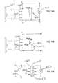
- FIG. 10is a simplified diagram of a matching network configured to power the coil of an inductive applicator module using balanced phase and antiphase voltages.
- a plasma processing apparatuscomprises a process chamber and a radiofrequency inductive plasma applicator at a wall of the chamber.
- the inductive plasma applicatorcomprises one or more radiofrequency inductive coupling elements (ICEs).
- the apparatusalso has one or more thin dielectric windows on the applicator wall. One of the thin dielectric windows isolates each ICE from the gas of a substantially inductive plasma wholly in the interior of the chamber.
- the plasmareceives inductive power coupled through the thin dielectric windows from the ICEs. Close proximity between each ICE and the process gas effectuates a relatively high degree of coupling with the plasma.
- the thin windowsare relatively narrow so that they can provide sufficient mechanical strength to support external atmospheric pressure when there is vacuum in the chamber.
- Various embodimentsprovide a high power transfer efficiency from the RF power source and/or applicator to the plasma.
- plasma uniformityis obtained with selective powering of various ICEs.
- an ICEincludes a coil.
- RF current flow through an ICE from an RF power sourceinduces an electromagnetic field that is localized within a relatively limited zone proximate to the coupling element.
- the electromagnetic field of a coupling elementis relatively attenuated beyond the localized zone.
- major structural and load bearing portions of an applicator wall in zones not subject to an intense RF fieldcan be comprised of relatively strong and/or inexpensive materials that are not well suited for being in a strong RF field or for coupling power from the ICEs.
- aluminum, steels, polar materials such as polyvinyl chloride or epoxy, and/or various compositescan be used in the load bearing portions.
- an applicator wall of the chamberis made using a thick dielectric fabricated with unitary thin windows (see, for example, thin window portion 190 of the lower applicator wall dielectric 110 in FIG. 1 ).
- Other embodimentshave at least one thin and relatively narrow discrete dielectric window segment in a recess and/or channel of a relatively thick, load bearing chamber wall.
- the thin dielectric window in the recessis interposed between an ICE and the plasma processing chamber.
- the thin window and receiving channel widthare sufficiently narrow to allow the relatively thin dielectric window to withstand atmospheric pressure.
- the chamber profileis approximately a circular cylinder and the coil and the dielectric window are positioned at a flat upper end of the cylindrical chamber.
- chamber shapedoes not limit the scope of the claims.
- the cross-section of the chambercan be rectangular, elliptical, polygonal, and others.
- a relatively higher coupling coefficient between an external applicator and ICP in a chamberis attained as distance between the applicator and interior of the chamber is reduced.
- a thin windowallows the applicator to be relatively proximate to the process gas in which an ICP is sustained in the processing chamber.
- a relatively high coupling coefficient between the applicator and ICPgenerally results in more efficient power transfer.
- various inductive coupling elementscan be selectively energized.
- different selected amounts of power in a selected phase relationshipare coupled to the various inductive coupling elements of the applicator and effect a predetermined spatial distribution of plasma density and/or potential.
- selected amounts of powerare transferred from various element coils in a manner that results in a relatively uniform plasma density.
- selective amounts of phase and antiphase powerare coupled in a manner to maintain an ICP within a preselected voltage from ground potential. The amounts of phase and antiphase power can be balanced with respect to a ground potential to mitigate and/or substantially eliminate capacitive current between the plasma and the inductively coupled applicator.
- modulerefers to a distinct unit that is operable to perform an identifiable function.
- a modulecan be a self-contained physical unit or piece of equipment.
- a modulecan also be a logical component effectuated by a processor and tangible media having instructions and/or data that are operable for the processor to perform the identifiable function.
- the term automaticrefers to a module, service, or control system that is operable to perform with no human interaction.
- gas or gas phase speciesas used herein includes species not bound to each other that have thermal and/or directed motion, and is not limited by a mean free path between collisions. Hence the term includes atomic or molecular beams, species in a vacuum, and the like.
- radiofrequencyrefers to an oscillation frequency between approximately 50 kHz and 5,000 GHz. Hence the term includes electromagnetic waves having very long wavelengths in air as well as those having millimeter wavelengths.
- applicatorrefers to a device for coupling radiofrequency electromagnetic energy into a plasma.
- An applicatorcan comprise inductive elements such as coils, capacitance coupled to a plasma, and/or means for launching a propagating electromagnetic wave.
- An inductive applicatorrefers to an applicator that is operable to couple energy to a plasma predominantly with a time-varying magnetic field.
- various terms denoting spatial positionsuch as above, below, upper, lower, leftmost, rightmost and the like are to be understood in a relative sense.
- the various aspects of the apparatuses described hereinare operable without regard to the spatial orientation of the apparatuses as a whole.
- an apparatuscan be configured in a vertical orientation or in a horizontal orientation.
- a component or module that is described as being above another component or module in a first embodiment having a first orientationcould equivalently be described as being to the left of the other component or module in an equivalent second embodiment configured to be in a second orientation 90 degrees counterclockwise with respect to the first.
- An inverted U-shaped cross sectionrefers to a cross section that has a substantially continuous top joining with two approximately lateral sides having approximately equal length. This term will be understood to include cross sections such as those through an inverted glass or cup, as well as the cross section of a rotationally symmetric recess cut into one side of a plate. In some aspects, this type of cross section can also be referenced as a c-shaped cross section.
- the apparatusincludes a processing chamber 100 having an interior volume 185 , an upper applicator wall portion 150 and a lower applicator wall portion 110 .
- the processing chamber cross sectionis generally circular as can be seen with respect to the view shown in FIG. 2 of circular lower applicator wall portion 110 .
- the processing chambercan be rectangular, hexagonal, and other shapes. The shape of the chamber and corresponding applicator wall do not limit the scope of the claims.
- the apparatusincludes a plasma applicator comprising at least one ICE.
- the lower applicator wall portion 110includes a number of recesses 155 for ICEs of the inductive plasma applicator.
- the ICEscomprise magnetic flux concentrators 160 and conductors 180 .
- Each of the ICEsis proximate to interior wall 115 of the chamber.
- Interior wall 115comprises associated thin window portions 190 and the lower surface of applicator wall portion 110 .
- a substrate 140is held on a substrate holder 130 in the chamber for processing with the inductive plasma processing apparatus.
- each windowis much smaller than the span of the chamber.
- a relatively thin strip windowcan withstand a pressure that would rupture a large uniformly thin window.
- a wafer substrate 300 millimeters in diameteris processed and the span of the chamber (a diameter of an applicator wall comprised of an upper portion 150 and a lower portion 110 ) is more than 300 mm.
- a thin strip window less than 5 millimeters thickis used and an associated ICE is positioned immediately adjacent to the window.
- ICEsare very close to the chamber gas where inductive plasma current is induced.
- the relatively small distance between the ICE and current carrying portion of the plasmais associated with a relatively large the mutual coupling coefficient between the coupling element and the current path in the plasma.
- the distance between an ICE and gas in the chamberis about 3 millimeters, and the coupling coefficient is greater than 0.5. It also has been found that a high power transfer efficiency can be obtained when each ICE is relatively close to the plasma.
- the path of plasma current induced by the proximate ICEis relatively narrow and largely localized in a region of the chamber adjacent to that element.
- Plasma current path induced from a coupling element through a relatively thick conventional windowwas found to be distributed over a relatively large volume above the substrate and to extending a relatively large distance from the coupling element.
- feed gascan be continuously introduced through a plurality of feed gas holes 125 .
- the feed holescan receive process gas through tubular channels 190 .
- the interior volume of the chamber 100is maintained at low pressure.
- a preselected chamber pressurecan be maintained using conventional pressure sensing devices (capacitance manometers, ion gauges, liquid manometers, spinning rotor gauges, and others), pumps such as oil based pumps, dry mechanical pumps, diffusion pumps, and others, and pressure control means such as automatic feedback control systems and/or conventional manual controls.
- pressure sensing devicescapacitortance manometers, ion gauges, liquid manometers, spinning rotor gauges, and others
- pumpssuch as oil based pumps, dry mechanical pumps, diffusion pumps, and others
- pressure control meanssuch as automatic feedback control systems and/or conventional manual controls.
- the applicator wallcomprised of portions 150 and 110 , and the lateral chamber walls, can support a pressure differential of at least one atmosphere.
- each feed hole with respect to FIG. 1 and/or FIG. 2can be configured to admit a preselected flow rate of process gas to chamber 185 .
- each of the feed holes 175is separately coupled to a gas supply through an associated gas connection 170 on the top applicator wall.
- a number of “showerhead” feed holes on the inner face of the applicator wallare configured to receive processing gas from an internal manifold within the applicator wall (not shown).
- one manifoldsupplies feed gas to all of the holes.
- there are a plurality of manifolds within the top applicator wallEach of these manifolds supplies feed gas to preselected feed holes, and each manifold has an external connection to receive an independent flow of a feed gas.
- a flow of feed gas to each manifold and its associated feed holescan be independently adjusted to improve processing uniformity.
- Still further embodimentscomprise feed gas delivery means to deliver process gas through inlets at various other positions in the chamber.
- Inletscan be holes, slits, nozzles and/or other shapes.
- feed gasis introduced into the chamber through slits on the perimeter sidewall 120 of the chamber.
- feed gasis introduced through holes on the side of the substrate holder.
- Various aspects of the inventiondo not depend on delivering feed gas from gas delivery apertures between the ICEs at a chamber applicator wall.
- the material comprising upper applicator wall portion 150 with respect to FIG. 1can comprise a relatively strong material such as stainless steel, hastalloy, aluminum, titanium, various composite materials, and/or others, in single or in combination, with a thickness sufficient to support a predetermined differential pressure.
- pressure force on the lower applicator wall portion 110can be partly or wholly transferred to the upper applicator wall portion 150 .
- forcecan be transferred by way of mechanical and/or adhesive bonding between lower applicator wall portion 110 and upper applicator wall portion 150 .
- the chamber pressureis approximately vacuum and the force of atmospheric pressure on the lower applicator wall portion is supported with the upper applicator wall portion.
- the lower applicator wall portioncan be comprised of a relatively weak or brittle material such as a silica based glass, quartz, chemically resistant plastics, and/or others.
- an ICE 190can be within approximately 5 mm of the interior of the chamber 185 , and the dielectric window 190 associated with the respective ICE 190 can be less than 5 mm in thickness.
- the sidewalls 120 of the chamberare a stainless steel or aluminum alloy. However the embodiments do not depend on the sidewall material and non-dielectric portions of the chamber wall can be any composition having sufficient mechanical properties and chemical compatibility with the process.
- each ICE of the applicatoris energized with current from a conventional radiofrequency (RF) power source (not shown).
- RF currentflows from the power source through conductors 180 of the inductive coupling element thereby producing magnetic flux.
- Each ICEalso has a magnetic flux concentrator 160 .
- the magnetic flux concentratoris operable to reduce the magnetic flux resistance for magnetic flux lines in the ICE.
- a magnetic flux concentratorcan also confine and/or concentrate magnetic flux for circulating through the chamber volume.
- the magnetic flux circulated from the applicator through the chamber volumeis operable induce sufficient current through a plasma wholly within chamber volume 185 to maintain a substantially inductive stable plasma.
- the magnetic flux concentrator of an inductive coupling unitcan provide relatively high magnetic flux in a region of the chamber that is generally localized relatively close to the inductive coupling unit and associated window. In various embodiments the majority of the magnetic flux within the chamber from an ICE is localized between the associated window and substrate.
- the magnetic flux concentratorcomprises material having substantial magnetic permeability.
- a magnetic material permeability relative to vacuum of approximately 10 or greater at the RF power frequencyis substantial, although a relative permeability of approximately 40 or more is preferable.
- the materialcan be a low loss ferromagnetic material such as Q1, Q2, or Q3 Ni—Zn ferrite material which are commercially available from the National Magnetics Group, Inc. of Bethlehem, Pa., 4F1 or 4C4 material and the like made by the Ferroxcube Corp. of Eindhoven, The Netherlands, and other low loss magnetic materials.
- the loss factor of a ferromagnetic mediumdepends on the RF excitation frequency. Hence the suitability a material in any particular application depends on the selected power frequency.
- the conductorcan be a coil comprised of a low resistivity metal such as silver or copper.
- a low resistivity metalsuch as silver or copper.
- other metals or a composite conductorcan also be used.
- a coilcomprised of a high conductive layer copper film coated on a poor conductor such as iron or on a nonconductive material.
- the lower applicator wall portion 100is comprised of a dielectric material that is substantially transparent to electromagnetic fields from the ICEs of the applicator. Quartz, pyrex, sapphire, diamond, ceramic, fluoropolymer, and various other dielectric materials and/or composites can be used as the dielectric, depending on the embodiment.
- the term dielectricis intended to include various high resistance materials that absorb and/or reflect relatively little energy from the electromagnetic field of the inductive applicator.
- silicon carbide, silicon, and low loss composite materialsare useful dielectrics.
- a thin annular dielectric window 190is supported on lips 188 of lower applicator wall portion 110 .
- the lower applicator wall portion 110can be comprised of an insulating or conductive material with sufficient mechanical strength to sustain at least one atmospheric pressure.
- the lower applicator wall portioncan be configured to sustain atmospheric pressure when it is mechanically and/or adhesively bonded to upper applicator wall portion 150 .
- there are seals(not shown).
- gas tight sealscan have conventional o-rings, gaskets, polymeric material that is cross linked in situ, glass to metal solder, and others (not shown).
- applicator wallis unitary.
- only the ICEs recesses 155have covers.
- FIG. 4Ais a simplified drawing of some magnetic flux lines, 401 , 402 , 403 , 404 , around a conventional flat coil 480 carrying current.
- the coil in FIG. 4Ahas no magnetic flux concentrator.
- the magnetic field lines around this current carrying coilare generally symmetric, and, as illustrated, they extend an appreciable distance above and below the coil, and to each side of the coil. Magnetic field lines produced by this configuration are relatively diffuse. and there is relatively low field strength in the area immediately underneath the coil. When there is plasma beneath the coil illustrated in FIG. 4A , inductive coupling between the coil and plasma is relatively weak.
- FIG. 4Billustrates magnetic field lines when there is a magnetic flux concentrator 470 coupled to coil 480 .
- the substantially permeable magnetic flux concentratorreduces magnetic path resistance for magnetic flux lines in the concentrator medium. Owing in part to this effect, the magnetic flux concentrator is operable to confine or focus, in single or in combination, magnetic flux lines 401 , 402 , 403 , 404 resulting from current flow in the coil. The upper portions of magnetic flux lines 401 , 402 , and 403 are confined within the concentrator.
- the magnetic flux lines in FIG. 4Bare concentrated into the flux concentrator and emerge from the concentrator in a downward direction, extending relatively deeper into the space below the coil and providing a relatively more intense field in that space than that obtained in FIG. 4A .
- the magnetic flux concentratorcomprises an approximately inverted U-shape cross section over the coil.
- each leg of the inverted U-shapecan be proximate to a dielectric window and within five millimeters of the chamber interior.
- FIG. 5further illustrates an ICE in a recess of lower portion 150 of an applicator wall.
- a thin window 590is supported on lips 588 of the applicator wall.
- Current flowing through turns of flat coil 580produce magnetic flux lines 565 that are confined in inverted U-cross section magnetic flux concentrator 560 and focused into the chamber.
- the thin windowisolates the ICE from process gas and a plasma maintained in the chamber.
- Circulating magnetic flux lines 565are localized in a relatively limited volume near the coupling chamber volume.
- the circulating fluxinduces current flow and thereby injects power in a relatively localized plasma volume 585 in the vicinity of the applicator.
- power delivered to the applicatoris deposited predominately within a plasma volume localized close to the applicator.
- 80 percent or more of the magnetic flux circulated from each ICEis within five centimeters of the active coupling element.
- a magnetic flux concentrator and/or a coilcan have various other configurations.
- a magnetic concentratorcan have a rectangular cross section subtending only the top of a coil (e.g. without legs of a U along the sides of a coil), an inverted A-shape, and other configurations operable to reduce the magnetic path resistance for magnetic flux lines around a conductor.
- a magnetic flux concentratorcan comprise a unitary ring, a plurality of generally flat or U-shape segments, and others.
- the conductor in an applicatorcan have various configurations. For instance, the conductor can be a single turn, multiturn flat coil such as shown in FIG. 3 or FIG.
- a coilcomprising a plurality of turns in a round or rectangular bundle, and others.
- an inverted U-shape cross section comprising magnetic media around flat coilsuch as a cross section shown similar to that shown in FIGS. 1 , 3 , 4 B, and FIG. 6 is preferred in various applications.
- the plasma density profilecan be adjusted by selectively injecting power into the various regions of plasma in the vicinity of different applicators.
- a larger number of applicatorsprovides a relatively more spatial control of the plasma density distribution.
- a gascan be evacuated from the chamber 102 by compatible pumping means such as a roots blower, a turbomolecular pump, a “dry” mechanical pump, a diffusion pump, and/or others, in single or incombination.
- compatible pumping meanssuch as a roots blower, a turbomolecular pump, a “dry” mechanical pump, a diffusion pump, and/or others, in single or incombination.
- process gasessuch as, merely by way of example, helium, argon, chlorine, bromine, hydrogen, fluorohydrocarbons, nitrogen, oxygen, silane, disilane, nitrogen trifluoride, water vapor, ammonia, and mixtures thereof, are useful for plasma processing, depending on the application.
- gasesare not limiting and various other gases and mixtures of gases can be used, depending on the application.
- gasesare not limiting and various other gases and mixtures of gases can be used, depending on the application.
- various discrete pressures, a sequence of discrete pressures, and/or a predetermined continuously changing pressure as a function of timeare used for plasma processing in embodiments.
- FIG. 6is a simplified cross sectional view of a rectangular processing chamber in an ICP processing apparatus.
- a rectangular geometryis particularly suitable for processing panels such as flat panel displays, rectangular solar cells, and others.
- the apparatusincludes a plasma applicator comprising at least one ICE.
- the lower applicator wall portion 610includes a number of slots 655 for ICEs of the inductive plasma applicator and thin dielectric strip windows 690 .
- Each ICEcomprises a magnetic flux concentrator 660 and conductors arranged in an approximately planar array 680 (also referenced as a flat coil portion). Furthermore, each of the ICEs is associated with one thin dielectric strip window.
- a substrate 640is held on a substrate holder 630 in the chamber for processing.
- the thin dielectric strip windows 690are supported on lips 688 abutting the lower portion 610 of the applicator wall. In various embodiments, the thin dielectric strip windows are less than approximately 5 mm in thickness.
- Each ICEhas an inverted U-cross section magnetic flux concentrator 660 . Rectangular upper applicator wall portion 650 reinforces lower applicator wall portion 610 and serves as a protective cover for the ICEs. As shown in the perspective view in FIG. 6 , there can be interconnections 686 between corresponding conductors of coil portions 680 in pairs of adjacent ICEs 681 and 681 and 683 and 684 .
- ICEscan be connected and/or powered in alternative manners.
- the coil portions of each ICE in a pair of ICEs interconnected with respect to FIG. 7can be further interconnected with interconnections 687 and powered using a single RF power source 896 .
- a different power source 898can selectively power a separate pair of ICEs. Power delivered to each respective pair, and/or the relative phase of the power delivered to each pair, can be selectively adjusted to optimize plasma uniformity.
- separate RF power sources 896 and 898are shown in FIG. 8
- a single power source and conventional resonant and/or non-resonant power splitters and phase adjustment networksare operable to selectively deliver power to various ICEs and/or ICE pairs in a predetermined relative phase relationship.
- ICEscan be powered in different ways.
- FIG. 9shows an illustrative configuration where RF power is selectively delivered to each of four ICEs.
- a plurality of ICEscan be coupled in parallel, in series, or they can be combined into various combinations of series and parallel connections. The scope of the claims is not limited by any ICE connection topologies.
- Another aspect of the present inventionis to mitigate and/or eliminate capacitively coupled voltage from a conductor or coil of an ICE to the inductive plasma.
- a plasmaWhen a plasma is maintained in the chamber, there can be a space charge plasma sheath between the relatively conductive region of a plasma (i.e. such as a region represented by volume 585 in the simplified drawing shown in FIG. 5 ) and the inside wall of the chamber.
- a space charge plasma sheathbetween the relatively conductive region of a plasma (i.e. such as a region represented by volume 585 in the simplified drawing shown in FIG. 5 ) and the inside wall of the chamber.
- the terminals A-A of an ICE coilare powered using symmetrical phase and antiphase voltage 1030 that is balanced with respect to ground potential.
- the balanced voltage applied to the coil terminalis operable to produce a balanced symmetrical voltage distribution 1030 along the coil. Since the extents of momentary positive 1031 and negative 1032 voltages along the coil are approximately equal, relative amounts of momentary positive and negative capacitive currents to the plasma through parasitic capacitances 1060 is cancelled. In these aspects there is substantially no net capacitive current flow between the coil and the plasma. Hence ion bombardment associated with capacitive current can be mitigated and/or avoided in various embodiments.
- a true push-pull driveis applied to ends A-A of an ICE coil.
- the true push-pull drivecan be obtained using an output from balanced resonant-matching network such as obtained at ends A-A with respect to FIG. 10C .
- the circuit in FIG. 10Ccomprises a balun transformer 1024 having primary winding 1062 connected to an RF power source 1092 and secondary winding 1064 connected by way of two equal capacitors 1072 and 1074 to ICE coil 1066 in FIG. 10B .
- tap 1050is connected to ground potential.
- Capacitors 1072 and 1074form a resonant circuit with ICE coil 1066 having resonance close to the frequency of the RF power source.
- the ratio of turns of the primary and secondary windings of transformer 1024can be selected to match the coil, coupled with an associated flux concentrator and plasma load, to the output impedance of the RF power source.
- push-pull (symmetrical or balanced) drive of an ICE coil with phase and antiphase voltages applied to respective coil endsprovides equal magnitude but opposite phase capacitive current to the window near the coil ends.
- the dielectric constant of the window materialis relatively large (k>>1).
- the windowcan perform as a low impedance medium (somewhat analogous to the effect of a metallic shield at low frequency) that can short circuit an electrical field between positive and negative ends of an ICE conductor. It can be seen that the window medium is operable to effectively cancel a portion of the opposing capacitive currents from positive and negative portions of the coil.
- powered with a symmetrical voltage and/or a push-pull driveare not limited by the dielectric constant of the window and/or short circuiting an electrical field between positive and negative portions of an ICE conductor.
Landscapes
- Physics & Mathematics (AREA)
- Engineering & Computer Science (AREA)
- Plasma & Fusion (AREA)
- Chemical & Material Sciences (AREA)
- Analytical Chemistry (AREA)
- Electromagnetism (AREA)
- Spectroscopy & Molecular Physics (AREA)
- Plasma Technology (AREA)
- Drying Of Semiconductors (AREA)
Abstract
Description
- This application is a division of copending U.S. utility patent application Ser. No. 11/843,595 filed on Feb. 11, 2008 which claimed priority under 35 U.S.C. §119(e) from U.S. Provisional Patent Application Ser. No. 60/839,011 filed on Aug. 22, 2006, the entire contents of both of which are hereby incorporated by reference, and for which priority is claimed under 35 U.S.C. §120.
- The present invention relates to plasma generation and, more particularly to methods for device processing with inductive plasmas having high coupling efficiency.
- Inductively coupled plasmas (ICPs) are advantageously used in the manufacture of devices such as integrated circuits, micromechanical devices, flat panel displays, and others. Inductive coupling is often preferred over capacitive coupling because the current flow in an inductive plasma is driven by an electromotive force with no associated scalar voltage differences. Capacitive coupling, on the other hand, can increase plasma potential, thereby causing undesirable parasitic currents and/or discharges between the plasma and various surfaces within the chamber. Relatively large potentials can occur, causing ions to bombard surfaces at high energy, thereby sputtering the surfaces and/or injecting sputter contamination into the process chamber.
- Generally, ICPs for processing are maintained within a plasma processing apparatus comprising an applicator (often referred to as an antenna) which couples high frequency electromagnetic energy through a large dielectric window of a processing chamber. In some applications the applicator is a single coil. The dielectric window is generally relatively low loss material such as quartz, alumina, or another ceramic.
- Plasma processing is often performed at relatively low pressure. For example, a preselected operating pressure for plasma etching and/or plasma assisted chemical vapor deposition can be in the range of 0.1 milliTorr to 100 Torr, depending on the application. However pressures outside of this range are also operable in some applications.
- ICP processing apparatus often has a dielectric window spanning an upper surface of a processing chamber. Electromagnetic flux coupled through the dielectric window sustains an inductively coupled plasma in chamber gas below the window. A workpiece or substrate for processing is commonly supported on a horizontal substrate holder or chuck in the chamber. The dielectric window can be flat, although dome shaped windows have also be used in conventional ICP processing apparatus.
- In many applications, such as plasma etching or plasma assisted chemical vapor deposition for the fabrication of integrated circuits, it can be essential to maintain a relatively uniform plasma over the various areas of a substrate being processed. With regards to uniformity, a flat dielectric window is often preferred to a dome shape, since a flat widow provides relatively uniform distance between various portions of the plasma source and the workpiece on the substrate holder. Since gas pressure in the processing chamber can be substantially below one atmosphere, the top dielectric window must be thick enough to withstand mechanical stress arising from atmospheric pressure. Mechanical considerations require that the minimum thickness of the window is approximately proportionate to the window diameter. Where the chamber diameter is sufficient to process a 300 mm semiconductor wafer (approximately 0.5 m diameter), a planar quartz window must be at least a few cm thick to withstand atmospheric pressure.
- When processing a workpiece in conventional ICP equipment, there is generally a relatively large distance between the external applicator and plasma in the chamber. Coupling between the applicator and ICP is relatively weak when the distance from applicator to plasma gas is relatively large. In general, RF power loss is more than proportionate to the applicator voltage. For example, RF power loss can increase in proportion to the square of the voltage applied to an applicator. Since weak coupling requires relatively high applicator voltage to transfer a predetermined amount of power to an ICP, it reduces the RF power transfer efficiency. Furthermore, relatively high power loss in the applicator and/or in the matching network is associated with ICP instability. Low efficiency has also made it difficult or unfeasible to maintain a low power and/or low density plasma in an inductive, rather than a capacitive mode. Hence it has been relatively difficult to perform processing at low power or at low plasma density with an ICP. Furthermore, ICP equipment has been burdened with costs of excess power supply capacity and the necessity of removing heat produced in power losses.
- Plasma uniformity control is also relatively difficult where there is a substantial separation between the applicator and plasma. In principle, spatial plasma uniformity in the chamber might be improved by using a plurality of applicator coils and directing various amounts of power into coils at different positions adjacent to the window. However there is generally poor spatial correlation between coil current and the adjacent plasma density related to substantial separation between the coils over a window and process gas interior to the chamber. Hence this technique has been relatively ineffective.
- Nonuniformity can also arise through nonuniform feed gas introduction. In some capacitive plasma processing equipment, an applicator electrode above a workpiece support has “showerhead” gas distribution holes for selectively introducing feed gas in a uniform manner. Generally, in ICP processing apparatus having an external inductive applicator above a workpiece, a large and relatively thick flat or dome-shaped dielectric window has been necessary to support external atmospheric pressure and allow magnetic flux into the chamber for powering the plasma. Such windows are have often been made from quartz or a ceramic. It has been impractical to introduce feed gas through large thick windows owing to structural/mechanical limitations and/or cost. Hence feed gas has been introduced into these chambers in a different manner. For example, in some ICP processing apparatus, feed gas has been introduced into the processing chamber through a plurality of feed injectors at various positions around the periphery of the substrate and/or below the substrate holder. However it has been relatively difficult to effect uniform gas distribution over the substrate using such means and injectors in the chamber can have adverse effects on plasma uniformity.
- It can be seen that there is a need for efficient ICP processing methods having relatively higher coupling between the applicator and plasma. There is also a need for ICP processing with improved power transfer efficiency and uniformity. Furthermore, there is a need for ICP processing methods that are operably stable at low power and/or low plasma density. Still further there is a need for ICP processing methods and apparatus with improved feed gas distribution.
- One aspect of the invention is a method of processing a substrate in the manufacture of a device. The method comprises placing a substrate having a film thereon on a substrate holder within a processing chamber of a processing apparatus and admitting a process gas into the interior of the chamber. The method further comprises maintaining a substantially inductive plasma wholly within the chamber using magnetic flux. The magnetic flux is produced by at energizing least one inductive plasma applicator outside of the processing chamber with radiofrequency power. The method further comprises performing at least one treatment of at least a portion of the film with the substantially inductive plasma in the chamber. The processing chamber comprises at least one or more thin windows less than approximately five millimeters in thickness on a wall of the chamber. The one inductive plasma applicator comprises one or more inductive coupling elements, operable to maintain the substantially inductive plasma wholly within the process gas in the interior of the chamber. In the method, each inductive coupling element among the one or more inductive coupling elements is associated with one thin window selected from among the one or more thin windows less than approximately five millimeters in thickness. Each inductive coupling element also can emit magnetic flux into the chamber interior and receive the magnetic flux returning from the chamber interior through the associated one thin window. At least one inductive coupling element among the one or more inductive coupling elements comprises a magnetic flux concentrator operable to reduce the magnetic path resistance for magnetic flux lines in the inductive coupling element.
- In an embodiment of the method, at least 80 percent of the magnetic flux circulated from the each inductive coupling unit into the chamber is within five centimeters of the thin window associated with the each inductive coupling element. In another embodiment, at least a portion of the substrate is within approximately five inches of at least one inductive coupling element selected from among the one or more inductive coupling elements. Furthermore, there is an embodiment where at least a portion of the substrate is within approximately two inches of at least one inductive coupling element selected from among the one or more inductive coupling elements.
- In another embodiment of the method at least one inductive coupling element comprises a coil. There is also an embodiment where at least one inductive coupling element comprises a flat coil portion. In a further embodiment at least one applicator comprises a magnetic flux concentrator operable to confine or focus the magnetic flux, in single or in combination. Also, there are embodiments where the magnetic flux concentrator comprises ferromagnetic material having a magnetic permeability relative to vacuum of at least 10 for the magnetic flux. In some of these, there is at least some ferromagnetic material adjacent to a coil portion. In some embodiments the magnetic flux concentrator comprises an approximately inverted U-shape cross section over the coil. An open side of the U-shape cross section faces the thin window associated with the inductive coupling element; and the end of each leg of the U-shape cross section is within approximately five millimeters of the chamber interior.
- Another aspect is an apparatus for processing a substrate using an inductive plasma. The apparatus comprises a processing chamber having an interior operable to confine a process gas, a substrate holder in the interior of the processing chamber operable to hold a substrate, and an inductive plasma applicator comprising one or more inductive coupling elements. The inductive plasma applicator is operable to maintain a substantially inductive plasma wholly within the process gas in the interior using radiofrequency power. The apparatus also comprises at least one or more thin windows less than five millimeters in thickness on a wall of the chamber operable to isolate an inductive coupling element from the process gas. In this aspect each inductive coupling element among the one or more inductive coupling elements is associated with a thin window selected from among the one or more thin windows less than five millimeters in thickness. At least a portion of each of the one or more inductive coupling elements is within five millimeters of the chamber interior. Each of the one or more inductive coupling elements is operable to emit magnetic flux into the chamber interior and to receive the magnetic flux returning from the chamber interior through the associated at least one thin window, whereby the magnetic flux circulates through the interior of the processing chamber.
- In various embodiments, the thin window is operable to support a pressure differential of at least one atmosphere. There are embodiments where at least one of the one or more inductive coupling elements comprises a coil portion. In further embodiments, at least one of the one or more inductive coupling elements comprises a magnetic flux concentrator operable to confine or focus, in single or in combination, magnetic flux emitted from the at least one inductive coupling element or received in the one or more inductive coupling element, in single or in combination. In embodiments the magnetic flux concentrator comprises ferromagnetic material having a magnetic permeability relative to vacuum of at least 10 for the magnetic flux.
- There is an embodiment where the magnetic flux concentrator comprises an approximately inverted U-shape cross section over the coil. In this embodiment an open side of the U-shape cross section faces the thin window associated with the inductive coupling element and the end of each leg of the U-shape cross section is within approximately five millimeters of the chamber interior.
- A further aspect is an apparatus for processing a substrate using an inductive plasma comprising a processing chamber having an interior operable to confine a process gas, and a substrate holder in the interior of the processing chamber operable to hold a substrate. This aspect also includes an inductive radiofrequency plasma applicator comprising one or more inductive coupling elements over the substrate within five millimeters of the interior of the chamber. The inductive plasma applicator is operable to maintain a substantially inductive plasma wholly within the process gas in the interior of the chamber. The aspect still further comprises a plurality of thin dielectric windows less than approximately five millimeters in thickness, an applicator wall over the substrate comprising a plurality of recesses for the external inductive coupling elements, and a plurality of feed gas holes interspersed among the inductively coupled elements over the substrate;
- Each recess selected from among the plurality of recesses is operable to receive at least one thin dielectric window, selected from among the plurality of thin dielectric windows, at an interior wall of the chamber, and receive least one inductive coupling element, selected from among of the one or more inductive coupling elements, in a position adjacent to the selected thin window within approximately five millimeters of the chamber interior. Also the at least one selected thin dielectric window is operable to isolate the at least one selected inductive coupling element from the process gas and support a pressure differential of at least one atmosphere. Furthermore each of the one or more inductive coupling elements is operable to emit magnetic flux into the interior of the processing chamber and to receive the magnetic flux returning from the interior of the processing chamber through the associated at least one thin window. Hence the magnetic flux circulates through the interior of the processing chamber.
- In various embodiments of the aspect, at least one of the one or more inductive coupling elements comprises a magnetic flux concentrator. The magnetic flux concentrator is operable to confine or focus, in single or in combination, magnetic flux emitted from the at least one inductive coupling element or received in the one or more inductive coupling element, in single or in combination. There are embodiments where the magnetic flux concentrator comprises ferromagnetic material having a magnetic permeability relative to vacuum of at least 10 for the magnetic flux.
- In some embodiments a processing chamber cross section is approximately polygonal. Also, in various embodiments, the substrate holder is operable to hold the substrate within approximately five inches of at least one inductive coupling element selected from among the one or more inductive coupling elements. Furthermore, there are embodiments where the apparatus is operable to deliver a first preselected flow rate of a feed gas through first feed gas holes selected from among the plurality of feed gas holes, and to deliver a second preselected flow rate of the feed gas through second feed gas holes selected from among the plurality of feed holes.
- Various embodiments are illustrated in an exemplary manner by the accompanying drawings. The drawings and accompanying description should be understood to explain principles of the embodiments rather than be limiting. Other embodiments will become apparent from the description and the drawings:
FIG. 1 is a simplified cross-sectional view of a portion of an inductive plasma processing chamber.FIG. 2 is a simplified inside view of the top of a circular processing chamber, in a relation toFIG. 1 .FIG. 3 is a simplified cross-sectional view of another embodiment of an inductive plasma processing chamber.FIG. 4 ais a simplified drawing of magnetic flux lines surrounding a current carrying flat coil.FIG. 4 bis a simplified drawing of magnetic flux lines surrounding a current carrying flat coil with a magnetic flux concentrator.FIG. 5 is a simplified view of a portion of one inductive coupling unit according toFIG. 3 , showing some magnetic flux lines and plasma current within the lines.FIG. 6 is a simplified cross-sectional view of a portion of another embodiment of a inductive plasma processing chamber.FIG. 7 is a simplified perspective view showing a portion of a portion of a plasma processing apparatus having a rectangular shape, in a relation toFIG. 6 .FIG. 8 is a simplified top view of another embodiment of a coil applicator over strip windows.FIG. 9 is a simplified diagram of another embodiment of a coil applicator over strip windows.FIG. 10 is a simplified diagram of a matching network configured to power the coil of an inductive applicator module using balanced phase and antiphase voltages.- Methods and apparatus for processing with an RF inductive plasma are disclosed. In some aspects, there is enhanced coupling between an inductive plasma applicator and plasma. In embodiments, a plasma processing apparatus comprises a process chamber and a radiofrequency inductive plasma applicator at a wall of the chamber. The inductive plasma applicator comprises one or more radiofrequency inductive coupling elements (ICEs). The apparatus also has one or more thin dielectric windows on the applicator wall. One of the thin dielectric windows isolates each ICE from the gas of a substantially inductive plasma wholly in the interior of the chamber. The plasma receives inductive power coupled through the thin dielectric windows from the ICEs. Close proximity between each ICE and the process gas effectuates a relatively high degree of coupling with the plasma.
- In various aspects the thin windows are relatively narrow so that they can provide sufficient mechanical strength to support external atmospheric pressure when there is vacuum in the chamber. Various embodiments provide a high power transfer efficiency from the RF power source and/or applicator to the plasma. Furthermore, in some embodiments plasma uniformity is obtained with selective powering of various ICEs.
- In various embodiments an ICE includes a coil. RF current flow through an ICE from an RF power source induces an electromagnetic field that is localized within a relatively limited zone proximate to the coupling element. The electromagnetic field of a coupling element is relatively attenuated beyond the localized zone. Accordingly, major structural and load bearing portions of an applicator wall in zones not subject to an intense RF field can be comprised of relatively strong and/or inexpensive materials that are not well suited for being in a strong RF field or for coupling power from the ICEs. For example, aluminum, steels, polar materials such as polyvinyl chloride or epoxy, and/or various composites can be used in the load bearing portions.
- In some embodiments an applicator wall of the chamber is made using a thick dielectric fabricated with unitary thin windows (see, for example,
thin window portion 190 of the lowerapplicator wall dielectric 110 inFIG. 1 ). Other embodiments have at least one thin and relatively narrow discrete dielectric window segment in a recess and/or channel of a relatively thick, load bearing chamber wall. The thin dielectric window in the recess is interposed between an ICE and the plasma processing chamber. The thin window and receiving channel width are sufficiently narrow to allow the relatively thin dielectric window to withstand atmospheric pressure. - In some embodiments the chamber profile is approximately a circular cylinder and the coil and the dielectric window are positioned at a flat upper end of the cylindrical chamber. However, chamber shape does not limit the scope of the claims. In further embodiments the cross-section of the chamber can be rectangular, elliptical, polygonal, and others.
- In general, a relatively higher coupling coefficient between an external applicator and ICP in a chamber is attained as distance between the applicator and interior of the chamber is reduced. In various embodiments, a thin window allows the applicator to be relatively proximate to the process gas in which an ICP is sustained in the processing chamber. A relatively high coupling coefficient between the applicator and ICP generally results in more efficient power transfer.
- In further embodiments, various inductive coupling elements can be selectively energized. In some embodiments, different selected amounts of power in a selected phase relationship are coupled to the various inductive coupling elements of the applicator and effect a predetermined spatial distribution of plasma density and/or potential. For example, in some embodiments selected amounts of power are transferred from various element coils in a manner that results in a relatively uniform plasma density. Furthermore, in some embodiments selective amounts of phase and antiphase power are coupled in a manner to maintain an ICP within a preselected voltage from ground potential. The amounts of phase and antiphase power can be balanced with respect to a ground potential to mitigate and/or substantially eliminate capacitive current between the plasma and the inductively coupled applicator.
- The terminology herein is for the purpose of describing particular embodiments and is not intended to be limiting of the invention. It will be understood that, although the terms first, second, etc. may be used to describe various elements, these terms are only used to distinguish one element from another and the elements should not be limited by these terms. For example, a first element could be termed a second element, and similarly a second element could be termed a first element, without departing from the scope of the instant description. As used herein, the singular forms “a”, “an” and “the” are intended to include the plural forms as well, unless the context clearly indicates otherwise. It will be further understood that the terms “comprises,” “comprising,” “includes,” “including,” and/or “having,” as used herein, are open-ended terms of art that signify the presence of stated features, integers, steps, operations, elements, and/or components, but do not preclude the presence or addition of one or more other features, integers, steps, operations, elements, components, and/or groups thereof. Reference in the specification to “one embodiment”, “an embodiment”, or some embodiment, etc. means that a particular feature, structure, or characteristic described in connection with the embodiment is included in at least one embodiment. The appearances of the phrase “in one embodiment” in various places in the specification are not necessarily all referring to the same embodiment, nor are separate or alternative embodiments mutually exclusive of other embodiments.
- The term module refers to a distinct unit that is operable to perform an identifiable function. A module can be a self-contained physical unit or piece of equipment. A module can also be a logical component effectuated by a processor and tangible media having instructions and/or data that are operable for the processor to perform the identifiable function. The term automatic refers to a module, service, or control system that is operable to perform with no human interaction.
- The term gas or gas phase species as used herein includes species not bound to each other that have thermal and/or directed motion, and is not limited by a mean free path between collisions. Hence the term includes atomic or molecular beams, species in a vacuum, and the like.
- The term radiofrequency as used herein refers to an oscillation frequency between approximately 50 kHz and 5,000 GHz. Hence the term includes electromagnetic waves having very long wavelengths in air as well as those having millimeter wavelengths. The term applicator refers to a device for coupling radiofrequency electromagnetic energy into a plasma. An applicator can comprise inductive elements such as coils, capacitance coupled to a plasma, and/or means for launching a propagating electromagnetic wave. An inductive applicator refers to an applicator that is operable to couple energy to a plasma predominantly with a time-varying magnetic field.
- As used here, various terms denoting spatial position such as above, below, upper, lower, leftmost, rightmost and the like are to be understood in a relative sense. The various aspects of the apparatuses described herein are operable without regard to the spatial orientation of the apparatuses as a whole. For example, an apparatus can be configured in a vertical orientation or in a horizontal orientation. Hence a component or module that is described as being above another component or module in a first embodiment having a first orientation, could equivalently be described as being to the left of the other component or module in an equivalent second embodiment configured to be in a second orientation 90 degrees counterclockwise with respect to the first.
- An inverted U-shaped cross section refers to a cross section that has a substantially continuous top joining with two approximately lateral sides having approximately equal length. This term will be understood to include cross sections such as those through an inverted glass or cup, as well as the cross section of a rotationally symmetric recess cut into one side of a plate. In some aspects, this type of cross section can also be referenced as a c-shaped cross section.
- The present teachings may be embodied in various different forms. In the following description, for purposes of explanation, numerous specific details are set forth in the description and drawings in order to provide a thorough understanding of the various principles. Furthermore, in various instances, structures and devices are described and/or drawn in simplified form in order to avoid obscuring the concepts. However, it will be apparent to one skilled in the art that the principles can be practiced in various different forms without these specific details. Hence aspects of the disclosure should not be construed as being limited to the embodiments set forth herein.
- A number of aspects can be understood with reference to the simplified cross-sectional diagram of an ICP processing apparatus in
FIG. 1 . The apparatus includes aprocessing chamber 100 having aninterior volume 185, an upperapplicator wall portion 150 and a lowerapplicator wall portion 110. In various embodiments, the processing chamber cross section is generally circular as can be seen with respect to the view shown inFIG. 2 of circular lowerapplicator wall portion 110. However in other aspects the processing chamber can be rectangular, hexagonal, and other shapes. The shape of the chamber and corresponding applicator wall do not limit the scope of the claims. - The apparatus includes a plasma applicator comprising at least one ICE. The lower
applicator wall portion 110 includes a number of recesses155 for ICEs of the inductive plasma applicator. The ICEs comprisemagnetic flux concentrators 160 andconductors 180. Each of the ICEs is proximate tointerior wall 115 of the chamber.Interior wall 115 comprises associatedthin window portions 190 and the lower surface ofapplicator wall portion 110. Asubstrate 140 is held on asubstrate holder 130 in the chamber for processing with the inductive plasma processing apparatus. - The width of each window is much smaller than the span of the chamber. A relatively thin strip window can withstand a pressure that would rupture a large uniformly thin window. For example, in various embodiments relative to
FIG. 1 and/orFIG. 2 , a wafer substrate 300 millimeters in diameter is processed and the span of the chamber (a diameter of an applicator wall comprised of anupper portion 150 and a lower portion110) is more than 300 mm. In these embodiments a thin strip window less than 5 millimeters thick is used and an associated ICE is positioned immediately adjacent to the window. Hence ICEs are very close to the chamber gas where inductive plasma current is induced. - The relatively small distance between the ICE and current carrying portion of the plasma is associated with a relatively large the mutual coupling coefficient between the coupling element and the current path in the plasma. For example, in one embodiment the distance between an ICE and gas in the chamber is about 3 millimeters, and the coupling coefficient is greater than 0.5. It also has been found that a high power transfer efficiency can be obtained when each ICE is relatively close to the plasma.
- Still further, the path of plasma current induced by the proximate ICE is relatively narrow and largely localized in a region of the chamber adjacent to that element. Plasma current path induced from a coupling element through a relatively thick conventional window (greater than about a centimeter in thickness), on the other hand, was found to be distributed over a relatively large volume above the substrate and to extending a relatively large distance from the coupling element.
- In a number of embodiments, feed gas can be continuously introduced through a plurality of feed gas holes125. The feed holes can receive process gas through
tubular channels 190. In some processing applications, the interior volume of thechamber 100 is maintained at low pressure. A preselected chamber pressure can be maintained using conventional pressure sensing devices (capacitance manometers, ion gauges, liquid manometers, spinning rotor gauges, and others), pumps such as oil based pumps, dry mechanical pumps, diffusion pumps, and others, and pressure control means such as automatic feedback control systems and/or conventional manual controls. The various aspects do not depend on having any specific type of pumping system, pressure sensing means, or a preselected pressure. In vacuum processing applications, the applicator wall, comprised ofportions - It has been found that introducing feed gas through holes interspersed among ICEs over the substrate provides excellent process uniformity. Illustrative distributions of feed holes among the ICEs are shown in
FIG. 1 andFIG. 2 . However different numbers and distributions of holes are useful in further embodiments. Furthermore, in some applications, process uniformity is improved where different feed gas flow rates are directed to the various holes. For example each feed hole with respect toFIG. 1 and/orFIG. 2 can be configured to admit a preselected flow rate of process gas tochamber 185. - In various embodiments with respect to
FIG. 1 , each of the feed holes175 is separately coupled to a gas supply through an associatedgas connection 170 on the top applicator wall. However some embodiments have other configurations. For example, there are embodiments where a number of “showerhead” feed holes on the inner face of the applicator wall are configured to receive processing gas from an internal manifold within the applicator wall (not shown). In some of these embodiments one manifold supplies feed gas to all of the holes. In different embodiments, there are a plurality of manifolds within the top applicator wall. Each of these manifolds supplies feed gas to preselected feed holes, and each manifold has an external connection to receive an independent flow of a feed gas. Hence a flow of feed gas to each manifold and its associated feed holes can be independently adjusted to improve processing uniformity. - Still further embodiments comprise feed gas delivery means to deliver process gas through inlets at various other positions in the chamber. Inlets can be holes, slits, nozzles and/or other shapes. For example, there is an embodiment where feed gas is introduced into the chamber through slits on the
perimeter sidewall 120 of the chamber. In a further embodiment, feed gas is introduced through holes on the side of the substrate holder. In some of these further embodiments, there are no feedholes interspersed among ICEs on the top applicator wall. Various aspects of the invention do not depend on delivering feed gas from gas delivery apertures between the ICEs at a chamber applicator wall. - The material comprising upper
applicator wall portion 150 with respect toFIG. 1 can comprise a relatively strong material such as stainless steel, hastalloy, aluminum, titanium, various composite materials, and/or others, in single or in combination, with a thickness sufficient to support a predetermined differential pressure. In various embodiments, pressure force on the lowerapplicator wall portion 110 can be partly or wholly transferred to the upperapplicator wall portion 150. For example, force can be transferred by way of mechanical and/or adhesive bonding between lowerapplicator wall portion 110 and upperapplicator wall portion 150. In some applications, the chamber pressure is approximately vacuum and the force of atmospheric pressure on the lower applicator wall portion is supported with the upper applicator wall portion. Hence the lower applicator wall portion can be comprised of a relatively weak or brittle material such as a silica based glass, quartz, chemically resistant plastics, and/or others. In various embodiments anICE 190 can be within approximately 5 mm of the interior of thechamber 185, and thedielectric window 190 associated with therespective ICE 190 can be less than 5 mm in thickness. In some embodiments thesidewalls 120 of the chamber are a stainless steel or aluminum alloy. However the embodiments do not depend on the sidewall material and non-dielectric portions of the chamber wall can be any composition having sufficient mechanical properties and chemical compatibility with the process. - For processing, each ICE of the applicator is energized with current from a conventional radiofrequency (RF) power source (not shown). RF current flows from the power source through
conductors 180 of the inductive coupling element thereby producing magnetic flux. Each ICE also has amagnetic flux concentrator 160. The magnetic flux concentrator is operable to reduce the magnetic flux resistance for magnetic flux lines in the ICE. A magnetic flux concentrator can also confine and/or concentrate magnetic flux for circulating through the chamber volume. The magnetic flux circulated from the applicator through the chamber volume is operable induce sufficient current through a plasma wholly within chamber volume185 to maintain a substantially inductive stable plasma. In various embodiments, the magnetic flux concentrator of an inductive coupling unit can provide relatively high magnetic flux in a region of the chamber that is generally localized relatively close to the inductive coupling unit and associated window. In various embodiments the majority of the magnetic flux within the chamber from an ICE is localized between the associated window and substrate. - The magnetic flux concentrator comprises material having substantial magnetic permeability. In this regard a magnetic material permeability relative to vacuum of approximately 10 or greater at the RF power frequency is substantial, although a relative permeability of approximately 40 or more is preferable. The material can be a low loss ferromagnetic material such as Q1, Q2, or Q3 Ni—Zn ferrite material which are commercially available from the National Magnetics Group, Inc. of Bethlehem, Pa., 4F1 or 4C4 material and the like made by the Ferroxcube Corp. of Eindhoven, The Netherlands, and other low loss magnetic materials. Those of ordinary skill in the art will appreciate that the loss factor of a ferromagnetic medium depends on the RF excitation frequency. Hence the suitability a material in any particular application depends on the selected power frequency.
- The conductor can be a coil comprised of a low resistivity metal such as silver or copper. However other metals or a composite conductor can also be used. For example there are embodiments having a coil comprised of a high conductive layer copper film coated on a poor conductor such as iron or on a nonconductive material.
- The lower
applicator wall portion 100 is comprised of a dielectric material that is substantially transparent to electromagnetic fields from the ICEs of the applicator. Quartz, pyrex, sapphire, diamond, ceramic, fluoropolymer, and various other dielectric materials and/or composites can be used as the dielectric, depending on the embodiment. In this regard, the term dielectric is intended to include various high resistance materials that absorb and/or reflect relatively little energy from the electromagnetic field of the inductive applicator. In some embodiments, silicon carbide, silicon, and low loss composite materials are useful dielectrics. - Another embodiment of an inductive plasma processing apparatus can be described with respect to the simplified cross sectional diagram of
FIG. 3 . A thin annulardielectric window 190 is supported on lips188 of lowerapplicator wall portion 110. The lowerapplicator wall portion 110 can be comprised of an insulating or conductive material with sufficient mechanical strength to sustain at least one atmospheric pressure. Alternatively, the lower applicator wall portion can be configured to sustain atmospheric pressure when it is mechanically and/or adhesively bonded to upperapplicator wall portion 150. In various embodiments there are seals (not shown). For example, in a number of embodiments there is a gas tight seal betweenwindow 190 and the supporting lips of lowerapplicator wall portion 110. There can be a gas tight seal between upper and lowerapplicator wall portions reactor sidewalls 120 in some embodiments. Depending on the embodiment, gas tight seals can have conventional o-rings, gaskets, polymeric material that is cross linked in situ, glass to metal solder, and others (not shown). - Although an embodiment with respect to
FIG. 3 with upper and lower applicator wall portions has been described, upper and lower applicator wall portions do not limit the scope of the claims. There are aspects when applicator wall is unitary. For example, in various embodiments there is a unitary pressure bearingapplicator wall 110 having with noupper portion 150. However in some of these embodiments, there is a protective cover, such as a relatively thin metal, insulating, or composite cover on top of the unitary wall (in a position corresponding to150). In other embodiments, only the ICEs recesses155 have covers. - Various advantages of a magnetic flux concentrator can be further understood with reference to the simplified drawings in
FIGS. 4A and 4B .FIG. 4A is a simplified drawing of some magnetic flux lines,401,402,403,404, around a conventionalflat coil 480 carrying current. The coil inFIG. 4A has no magnetic flux concentrator. The magnetic field lines around this current carrying coil are generally symmetric, and, as illustrated, they extend an appreciable distance above and below the coil, and to each side of the coil. Magnetic field lines produced by this configuration are relatively diffuse. and there is relatively low field strength in the area immediately underneath the coil. When there is plasma beneath the coil illustrated inFIG. 4A , inductive coupling between the coil and plasma is relatively weak. - The drawing in
FIG. 4B illustrates magnetic field lines when there is amagnetic flux concentrator 470 coupled tocoil 480. The substantially permeable magnetic flux concentrator reduces magnetic path resistance for magnetic flux lines in the concentrator medium. Owing in part to this effect, the magnetic flux concentrator is operable to confine or focus, in single or in combination,magnetic flux lines magnetic flux lines FIG. 4B are concentrated into the flux concentrator and emerge from the concentrator in a downward direction, extending relatively deeper into the space below the coil and providing a relatively more intense field in that space than that obtained inFIG. 4A . In embodiments with respect toFIG. 4B , the magnetic flux concentrator comprises an approximately inverted U-shape cross section over the coil. In ICEs comprising a U-shape magnetic concentrator cross-section, each leg of the inverted U-shape can be proximate to a dielectric window and within five millimeters of the chamber interior. FIG. 5 further illustrates an ICE in a recess oflower portion 150 of an applicator wall. Athin window 590 is supported onlips 588 of the applicator wall. Current flowing through turns offlat coil 580 producemagnetic flux lines 565 that are confined in inverted U-cross sectionmagnetic flux concentrator 560 and focused into the chamber. The thin window isolates the ICE from process gas and a plasma maintained in the chamber. Circulatingmagnetic flux lines 565 are localized in a relatively limited volume near the coupling chamber volume. The circulating flux induces current flow and thereby injects power in a relativelylocalized plasma volume 585 in the vicinity of the applicator. Hence power delivered to the applicator is deposited predominately within a plasma volume localized close to the applicator. In various embodiment 80 percent or more of the magnetic flux circulated from each ICE is within five centimeters of the active coupling element.- In further embodiments a magnetic flux concentrator and/or a coil can have various other configurations. For example, a magnetic concentrator can have a rectangular cross section subtending only the top of a coil (e.g. without legs of a U along the sides of a coil), an inverted A-shape, and other configurations operable to reduce the magnetic path resistance for magnetic flux lines around a conductor. A magnetic flux concentrator can comprise a unitary ring, a plurality of generally flat or U-shape segments, and others. Also, the conductor in an applicator can have various configurations. For instance, the conductor can be a single turn, multiturn flat coil such as shown in
FIG. 3 orFIG. 4B , a coil comprising a plurality of turns in a round or rectangular bundle, and others. However an inverted U-shape cross section comprising magnetic media around flat coil, such as a cross section shown similar to that shown inFIGS. 1 ,3,4B, andFIG. 6 is preferred in various applications. - Having localized RF power injection in the vicinity of the inductive coupling element provides means for adjusting plasma uniformity. In various aspects, the plasma density profile can be adjusted by selectively injecting power into the various regions of plasma in the vicinity of different applicators. In general, a larger number of applicators provides a relatively more spatial control of the plasma density distribution. In a number of embodiments there is an ICE with approximately five inches of each portion of the substrate. In some embodiments there is an ICE within approximately two inches of each portion of the substrate.
- Depending on the application, single gases or a blend of process gases can be admitted to the process chamber. In various aspects a gas can be evacuated from the chamber102 by compatible pumping means such as a roots blower, a turbomolecular pump, a “dry” mechanical pump, a diffusion pump, and/or others, in single or incombination. Those of ordinary skill in the art will recognize that different process gases such as, merely by way of example, helium, argon, chlorine, bromine, hydrogen, fluorohydrocarbons, nitrogen, oxygen, silane, disilane, nitrogen trifluoride, water vapor, ammonia, and mixtures thereof, are useful for plasma processing, depending on the application. However these gases are not limiting and various other gases and mixtures of gases can be used, depending on the application. Furthermore, various discrete pressures, a sequence of discrete pressures, and/or a predetermined continuously changing pressure as a function of time are used for plasma processing in embodiments.
- Additional embodiments can be described with respect to the simplified diagrams in
FIG. 6 andFIG. 7 .FIG. 6 is a simplified cross sectional view of a rectangular processing chamber in an ICP processing apparatus. A rectangular geometry is particularly suitable for processing panels such as flat panel displays, rectangular solar cells, and others. The apparatus includes a plasma applicator comprising at least one ICE. The lowerapplicator wall portion 610 includes a number ofslots 655 for ICEs of the inductive plasma applicator and thindielectric strip windows 690. Each ICE comprises amagnetic flux concentrator 660 and conductors arranged in an approximately planar array680 (also referenced as a flat coil portion). Furthermore, each of the ICEs is associated with one thin dielectric strip window. Asubstrate 640 is held on asubstrate holder 630 in the chamber for processing. - The thin
dielectric strip windows 690 are supported onlips 688 abutting thelower portion 610 of the applicator wall. In various embodiments, the thin dielectric strip windows are less than approximately 5 mm in thickness. Each ICE has an inverted U-cross sectionmagnetic flux concentrator 660. Rectangular upperapplicator wall portion 650 reinforces lowerapplicator wall portion 610 and serves as a protective cover for the ICEs. As shown in the perspective view inFIG. 6 , there can beinterconnections 686 between corresponding conductors of coil portions680 in pairs ofadjacent ICEs - In various embodiments, ICEs can be connected and/or powered in alternative manners. With respect to
FIG. 8 , the coil portions of each ICE in a pair of ICEs interconnected with respect toFIG. 7 can be further interconnected with interconnections687 and powered using a singleRF power source 896. Adifferent power source 898 can selectively power a separate pair of ICEs. Power delivered to each respective pair, and/or the relative phase of the power delivered to each pair, can be selectively adjusted to optimize plasma uniformity. Although separateRF power sources FIG. 8 , a single power source and conventional resonant and/or non-resonant power splitters and phase adjustment networks are operable to selectively deliver power to various ICEs and/or ICE pairs in a predetermined relative phase relationship. - In further embodiments ICEs can be powered in different ways. For example,
FIG. 9 shows an illustrative configuration where RF power is selectively delivered to each of four ICEs. In still further embodiments, a plurality of ICEs can be coupled in parallel, in series, or they can be combined into various combinations of series and parallel connections. The scope of the claims is not limited by any ICE connection topologies. - Another aspect of the present invention is to mitigate and/or eliminate capacitively coupled voltage from a conductor or coil of an ICE to the inductive plasma. When a plasma is maintained in the chamber, there can be a space charge plasma sheath between the relatively conductive region of a plasma (i.e. such as a region represented by
volume 585 in the simplified drawing shown inFIG. 5 ) and the inside wall of the chamber. With respect toFIG. 10A , when thecoil 1065 of an ICE is powered in a single ended mode such as when exemplaryRF voltage source 1010 applies momentarily positive voltage distribution1020 oncoil 1065, the positive RF voltage on the coil can induce a net positive capacitive current from the coil to conductive regions1158 of the plasma throughparasitic capacitances 1060. Conversely, when the coil is momentarily negative, there can be a negative capacitive current flow from the coil to the plasma. Generally such currents are undesirable because they tend to increase the plasma potential and can intensify ion bombardment of chambers walls and other surfaces that are exposed to the plasma. Ion bombardment of chamber walls can cause wall erosion and contamination in a process. - In various aspects with respect to
FIG. 10B , the terminals A-A of an ICE coil are powered using symmetrical phase andantiphase voltage 1030 that is balanced with respect to ground potential. The balanced voltage applied to the coil terminal is operable to produce a balancedsymmetrical voltage distribution 1030 along the coil. Since the extents of momentary positive1031 and negative1032 voltages along the coil are approximately equal, relative amounts of momentary positive and negative capacitive currents to the plasma throughparasitic capacitances 1060 is cancelled. In these aspects there is substantially no net capacitive current flow between the coil and the plasma. Hence ion bombardment associated with capacitive current can be mitigated and/or avoided in various embodiments. - In some embodiments with respect to
FIG. 10B , a true push-pull drive is applied to ends A-A of an ICE coil. The true push-pull drive can be obtained using an output from balanced resonant-matching network such as obtained at ends A-A with respect toFIG. 10C . The circuit inFIG. 10C comprises abalun transformer 1024 having primary winding1062 connected to anRF power source 1092 and secondary winding1064 connected by way of twoequal capacitors 1072 and1074 toICE coil 1066 inFIG. 10B . Also,tap 1050 is connected to ground potential.Capacitors 1072 and1074 form a resonant circuit withICE coil 1066 having resonance close to the frequency of the RF power source. The ratio of turns of the primary and secondary windings oftransformer 1024 can be selected to match the coil, coupled with an associated flux concentrator and plasma load, to the output impedance of the RF power source. - It can be seen that push-pull (symmetrical or balanced) drive of an ICE coil with phase and antiphase voltages applied to respective coil ends, provides equal magnitude but opposite phase capacitive current to the window near the coil ends. In various embodiments the dielectric constant of the window material is relatively large (k>>1). At radio frequency, the window can perform as a low impedance medium (somewhat analogous to the effect of a metallic shield at low frequency) that can short circuit an electrical field between positive and negative ends of an ICE conductor. It can be seen that the window medium is operable to effectively cancel a portion of the opposing capacitive currents from positive and negative portions of the coil. However various embodiments powered with a symmetrical voltage and/or a push-pull drive are not limited by the dielectric constant of the window and/or short circuiting an electrical field between positive and negative portions of an ICE conductor.
- In the foregoing specification, various aspects are described with reference to specific embodiments, but those skilled in the art will recognize that further aspects are not limited thereto. Various features and aspects-described above may be used individually or jointly. Other aspects of the invention, including alternatives, modifications, permutations and equivalents of the embodiments described herein, will be apparent to those skilled in the art from consideration of the specification, study of the drawings, and practice of the various aspects. Further, various aspects can be utilized in any number of environments and applications beyond those described herein without departing from the broader spirit and scope of the description. The written description and accompanying drawings are, accordingly, to be regarded as illustrative rather than restrictive.
- The embodiments and preferred features described above should be considered exemplary, with the invention being defined by the appended claims, which therefore include all such alternatives, modifications, permutations and equivalents as fall within the true spirit and scope of the present disclosures.
Claims (25)
Priority Applications (1)
| Application Number | Priority Date | Filing Date | Title |
|---|---|---|---|
| US12/471,375US8444870B2 (en) | 2006-08-22 | 2009-05-23 | Inductive plasma source with high coupling efficiency |
Applications Claiming Priority (3)
| Application Number | Priority Date | Filing Date | Title |
|---|---|---|---|
| US83901106P | 2006-08-22 | 2006-08-22 | |
| US11/843,595US8920600B2 (en) | 2006-08-22 | 2007-08-22 | Inductive plasma source with high coupling efficiency |
| US12/471,375US8444870B2 (en) | 2006-08-22 | 2009-05-23 | Inductive plasma source with high coupling efficiency |
Related Parent Applications (1)
| Application Number | Title | Priority Date | Filing Date |
|---|---|---|---|
| US11/843,595DivisionUS8920600B2 (en) | 2006-08-22 | 2007-08-22 | Inductive plasma source with high coupling efficiency |
Publications (2)
| Publication Number | Publication Date |
|---|---|
| US20100136262A1true US20100136262A1 (en) | 2010-06-03 |
| US8444870B2 US8444870B2 (en) | 2013-05-21 |
Family
ID=39107381
Family Applications (3)
| Application Number | Title | Priority Date | Filing Date |
|---|---|---|---|
| US11/843,595Active2027-09-01US8920600B2 (en) | 2006-08-22 | 2007-08-22 | Inductive plasma source with high coupling efficiency |
| US12/471,375Active2028-04-25US8444870B2 (en) | 2006-08-22 | 2009-05-23 | Inductive plasma source with high coupling efficiency |
| US14/581,348ActiveUS10037867B2 (en) | 2006-08-22 | 2014-12-23 | Inductive plasma source with high coupling efficiency |
Family Applications Before (1)
| Application Number | Title | Priority Date | Filing Date |
|---|---|---|---|
| US11/843,595Active2027-09-01US8920600B2 (en) | 2006-08-22 | 2007-08-22 | Inductive plasma source with high coupling efficiency |
Family Applications After (1)
| Application Number | Title | Priority Date | Filing Date |
|---|---|---|---|
| US14/581,348ActiveUS10037867B2 (en) | 2006-08-22 | 2014-12-23 | Inductive plasma source with high coupling efficiency |
Country Status (3)
| Country | Link |
|---|---|
| US (3) | US8920600B2 (en) |
| EP (1) | EP2087778A4 (en) |
| WO (1) | WO2008024392A2 (en) |
Cited By (9)
| Publication number | Priority date | Publication date | Assignee | Title |
|---|---|---|---|---|
| US20080050292A1 (en)* | 2006-08-28 | 2008-02-28 | Valery Godyak | Plasma reactor with inductie excitation of plasma and efficient removal of heat from the excitation coil |
| WO2012087919A3 (en)* | 2010-12-20 | 2012-09-20 | Applied Materials, Inc. | Methods and apparatus for gas delivery into plasma processing chambers |
| US20140239729A1 (en)* | 2011-07-08 | 2014-08-28 | Auckland Uniservices Ltd. | Interoperability of magnetic structures for inductive power transfer systems |
| US8920600B2 (en) | 2006-08-22 | 2014-12-30 | Mattson Technology, Inc. | Inductive plasma source with high coupling efficiency |
| US20170316922A1 (en)* | 2016-04-27 | 2017-11-02 | Vni Solution Co., Ltd. | Gas supply structure for inductively coupled plasma processing apparatus |
| US9928992B2 (en)* | 2015-06-05 | 2018-03-27 | Panasonic Intellectual Property Management Co., Ltd. | Plasma generation device |
| CN108695132A (en)* | 2017-03-29 | 2018-10-23 | 细美事有限公司 | Plasma generation unit and substrate board treatment including it |
| US10297457B2 (en) | 2015-03-19 | 2019-05-21 | Mattson Technology, Inc. | Controlling azimuthal uniformity of etch process in plasma processing chamber |
| US20230352270A1 (en)* | 2019-12-16 | 2023-11-02 | Dyson Technology Limited | Method and apparatus for use in generating plasma |
Families Citing this family (72)
| Publication number | Priority date | Publication date | Assignee | Title |
|---|---|---|---|---|
| JP5252613B2 (en)* | 2006-12-25 | 2013-07-31 | 国立大学法人東北大学 | Ion implantation apparatus and ion implantation method |
| CN102027811B (en)* | 2008-05-22 | 2015-12-09 | Emd株式会社 | Plasma generating device and plasma processing device |
| TWI498053B (en)* | 2008-12-23 | 2015-08-21 | Ind Tech Res Inst | Plasma excitation module |
| JP4621287B2 (en)* | 2009-03-11 | 2011-01-26 | 株式会社イー・エム・ディー | Plasma processing equipment |
| JP5400434B2 (en)* | 2009-03-11 | 2014-01-29 | 株式会社イー・エム・ディー | Plasma processing equipment |
| US7994724B2 (en)* | 2009-03-27 | 2011-08-09 | Ecole Polytechnique | Inductive plasma applicator |
| KR101312695B1 (en)* | 2009-08-21 | 2013-09-27 | 맷슨 테크놀로지, 인크. | Inductive plasma source |
| US8501631B2 (en)* | 2009-11-19 | 2013-08-06 | Lam Research Corporation | Plasma processing system control based on RF voltage |
| US20110278260A1 (en)* | 2010-05-14 | 2011-11-17 | Applied Materials, Inc. | Inductive plasma source with metallic shower head using b-field concentrator |
| US20140150975A1 (en)* | 2010-09-06 | 2014-06-05 | Emd Corporation | Plasma processing device |
| CN103202105B (en)* | 2010-09-10 | 2015-11-25 | Emd株式会社 | Plasma treatment appts |
| JP5745812B2 (en)* | 2010-10-27 | 2015-07-08 | 東京エレクトロン株式会社 | Plasma processing equipment |
| WO2012082854A2 (en) | 2010-12-17 | 2012-06-21 | Mattson Technology, Inc. | Inductively coupled plasma source for plasma processing |
| CN102548180A (en)* | 2010-12-27 | 2012-07-04 | 北京北方微电子基地设备工艺研究中心有限责任公司 | Medium window, inductive coupling coil assembly, and plasma processing equipment |
| KR101246170B1 (en)* | 2011-01-13 | 2013-03-25 | 국제엘렉트릭코리아 주식회사 | Injection member used in manufacturing semiconductor device and plasma processing apparatus having the same |
| CN204117820U (en)* | 2011-03-09 | 2015-01-21 | 松下电器产业株式会社 | Non-contact charge module, non-contact charger and electronic equipment |
| TW201301335A (en)* | 2011-05-17 | 2013-01-01 | Intevac Inc | Large area ICP source for plasma application |
| KR101241049B1 (en) | 2011-08-01 | 2013-03-15 | 주식회사 플라즈마트 | Plasma generation apparatus and plasma generation method |
| US9034143B2 (en) | 2011-10-05 | 2015-05-19 | Intevac, Inc. | Inductive/capacitive hybrid plasma source and system with such chamber |
| KR101246191B1 (en)* | 2011-10-13 | 2013-03-21 | 주식회사 윈텔 | Plasma generation apparatus and substrate processing apparatus |
| US9320126B2 (en) | 2012-12-17 | 2016-04-19 | Lam Research Corporation | Determining a value of a variable on an RF transmission model |
| US10128090B2 (en) | 2012-02-22 | 2018-11-13 | Lam Research Corporation | RF impedance model based fault detection |
| US9197196B2 (en) | 2012-02-22 | 2015-11-24 | Lam Research Corporation | State-based adjustment of power and frequency |
| US9842725B2 (en) | 2013-01-31 | 2017-12-12 | Lam Research Corporation | Using modeling to determine ion energy associated with a plasma system |
| US10157729B2 (en) | 2012-02-22 | 2018-12-18 | Lam Research Corporation | Soft pulsing |
| US9114666B2 (en) | 2012-02-22 | 2015-08-25 | Lam Research Corporation | Methods and apparatus for controlling plasma in a plasma processing system |
| US9462672B2 (en) | 2012-02-22 | 2016-10-04 | Lam Research Corporation | Adjustment of power and frequency based on three or more states |
| DE102012013534B3 (en) | 2012-07-05 | 2013-09-19 | Tobias Sokolowski | Apparatus for repetitive nerve stimulation for the degradation of adipose tissue by means of inductive magnetic fields |
| US9594105B2 (en) | 2014-01-10 | 2017-03-14 | Lam Research Corporation | Cable power loss determination for virtual metrology |
| US10950421B2 (en) | 2014-04-21 | 2021-03-16 | Lam Research Corporation | Using modeling for identifying a location of a fault in an RF transmission system for a plasma system |
| US11491342B2 (en) | 2015-07-01 | 2022-11-08 | Btl Medical Solutions A.S. | Magnetic stimulation methods and devices for therapeutic treatments |
| US20180001107A1 (en) | 2016-07-01 | 2018-01-04 | Btl Holdings Limited | Aesthetic method of biological structure treatment by magnetic field |
| US10695575B1 (en) | 2016-05-10 | 2020-06-30 | Btl Medical Technologies S.R.O. | Aesthetic method of biological structure treatment by magnetic field |
| US11266850B2 (en) | 2015-07-01 | 2022-03-08 | Btl Healthcare Technologies A.S. | High power time varying magnetic field therapy |
| US11253717B2 (en) | 2015-10-29 | 2022-02-22 | Btl Healthcare Technologies A.S. | Aesthetic method of biological structure treatment by magnetic field |
| US10431425B2 (en)* | 2016-02-23 | 2019-10-01 | Tokyo Electron Limited | Poly-phased inductively coupled plasma source |
| JP6122169B1 (en)* | 2016-03-15 | 2017-04-26 | 株式会社東芝 | Processing device and collimator |
| US11464993B2 (en) | 2016-05-03 | 2022-10-11 | Btl Healthcare Technologies A.S. | Device including RF source of energy and vacuum system |
| US11247039B2 (en) | 2016-05-03 | 2022-02-15 | Btl Healthcare Technologies A.S. | Device including RF source of energy and vacuum system |
| US11534619B2 (en) | 2016-05-10 | 2022-12-27 | Btl Medical Solutions A.S. | Aesthetic method of biological structure treatment by magnetic field |
| US10583287B2 (en) | 2016-05-23 | 2020-03-10 | Btl Medical Technologies S.R.O. | Systems and methods for tissue treatment |
| US10128083B2 (en)* | 2016-06-01 | 2018-11-13 | Vebco Instruments Inc. | Ion sources and methods for generating ion beams with controllable ion current density distributions over large treatment areas |
| US10556122B1 (en) | 2016-07-01 | 2020-02-11 | Btl Medical Technologies S.R.O. | Aesthetic method of biological structure treatment by magnetic field |
| US11141219B1 (en) | 2016-08-16 | 2021-10-12 | BTL Healthcare Technologies, a.s. | Self-operating belt |
| US11749509B2 (en) | 2017-02-20 | 2023-09-05 | Beijing E-Town Semiconductor Technology, Co., Ltd | Temperature control using temperature control element coupled to faraday shield |
| US10790119B2 (en) | 2017-06-09 | 2020-09-29 | Mattson Technology, Inc | Plasma processing apparatus with post plasma gas injection |
| US11201036B2 (en) | 2017-06-09 | 2021-12-14 | Beijing E-Town Semiconductor Technology Co., Ltd | Plasma strip tool with uniformity control |
| CN110800375B (en)* | 2017-06-27 | 2021-12-28 | 佳能安内华股份有限公司 | Plasma processing apparatus |
| TWI693860B (en) | 2017-06-27 | 2020-05-11 | 日商佳能安內華股份有限公司 | Plasma treatment device |
| JP6595002B2 (en) | 2017-06-27 | 2019-10-23 | キヤノンアネルバ株式会社 | Sputtering equipment |
| WO2019004192A1 (en) | 2017-06-27 | 2019-01-03 | キヤノンアネルバ株式会社 | Plasma processing device |
| PL3817517T3 (en) | 2018-06-26 | 2024-10-28 | Canon Anelva Corporation | Plasma treatment device, plasma treatment method, program, and memory medium |
| US11037765B2 (en)* | 2018-07-03 | 2021-06-15 | Tokyo Electron Limited | Resonant structure for electron cyclotron resonant (ECR) plasma ionization |
| JP7090521B2 (en)* | 2018-09-26 | 2022-06-24 | 東京エレクトロン株式会社 | Plasma processing equipment and plasma processing method |
| EP4387275A3 (en)* | 2018-09-28 | 2024-08-07 | GN Hearing A/S | Hearing device with antenna extending from the hearing device |
| JP7133123B2 (en)* | 2019-01-23 | 2022-09-08 | 株式会社島津製作所 | Dielectric barrier discharge ionization detector |
| US12156689B2 (en) | 2019-04-11 | 2024-12-03 | Btl Medical Solutions A.S. | Methods and devices for aesthetic treatment of biological structures by radiofrequency and magnetic energy |
| ES2926904T3 (en) | 2019-04-11 | 2022-10-31 | Btl Medical Solutions A S | Device for the aesthetic treatment of biological structures using radiofrequency and magnetic energy |
| US11189464B2 (en)* | 2019-07-17 | 2021-11-30 | Beijing E-town Semiconductor Technology Co., Ltd. | Variable mode plasma chamber utilizing tunable plasma potential |
| GB2590614B (en) | 2019-12-16 | 2022-09-28 | Dyson Technology Ltd | Method and apparatus for use in generating plasma |
| JP7394632B2 (en)* | 2020-01-16 | 2023-12-08 | 東京エレクトロン株式会社 | Array antenna and plasma processing equipment |
| WO2021224678A1 (en) | 2020-05-04 | 2021-11-11 | Btl Medical Technologies S.R.O. | Device and method for unattended treatment of a patient |
| US11878167B2 (en) | 2020-05-04 | 2024-01-23 | Btl Healthcare Technologies A.S. | Device and method for unattended treatment of a patient |
| US12068134B2 (en) | 2021-01-29 | 2024-08-20 | Applied Materials, Inc. | Digital control of plasma processing |
| US12027426B2 (en) | 2021-01-29 | 2024-07-02 | Applied Materials, Inc. | Image-based digital control of plasma processing |
| CN113223916B (en)* | 2021-06-09 | 2024-05-28 | 上海邦芯半导体科技有限公司 | Inductively coupled plasma device |
| TWI825711B (en) | 2021-06-25 | 2023-12-11 | 美商得昇科技股份有限公司 | Plasma processing apparatus |
| CN113851368B (en)* | 2021-09-22 | 2023-01-31 | 大连理工大学 | Method for enhancing discharge in radio frequency magnetization capacitive coupling discharge device |
| EP4415812A1 (en) | 2021-10-13 | 2024-08-21 | BTL Medical Solutions a.s. | Devices for aesthetic treatment of biological structures by radiofrequency and magnetic energy |
| US11896816B2 (en) | 2021-11-03 | 2024-02-13 | Btl Healthcare Technologies A.S. | Device and method for unattended treatment of a patient |
| US20240170261A1 (en)* | 2022-11-21 | 2024-05-23 | Applied Materials, Inc. | Plasma generator for edge uniformity |
| WO2025179485A1 (en)* | 2024-02-28 | 2025-09-04 | Arrayed Materials (China) Co., Ltd. | Inductively-coupled plasma (icp) source for rectangular substrate |
Citations (41)
| Publication number | Priority date | Publication date | Assignee | Title |
|---|---|---|---|---|
| US5234529A (en)* | 1991-10-10 | 1993-08-10 | Johnson Wayne L | Plasma generating apparatus employing capacitive shielding and process for using such apparatus |
| US5304282A (en)* | 1991-04-17 | 1994-04-19 | Flamm Daniel L | Processes depending on plasma discharges sustained in a helical resonator |
| US5309063A (en)* | 1993-03-04 | 1994-05-03 | David Sarnoff Research Center, Inc. | Inductive coil for inductively coupled plasma production apparatus |
| US5401350A (en)* | 1993-03-08 | 1995-03-28 | Lsi Logic Corporation | Coil configurations for improved uniformity in inductively coupled plasma systems |
| US5464476A (en)* | 1993-10-19 | 1995-11-07 | Central Research Laboratories Limited | Plasma processing device comprising plural RF inductive coils |
| US5571366A (en)* | 1993-10-20 | 1996-11-05 | Tokyo Electron Limited | Plasma processing apparatus |
| US5653811A (en)* | 1995-07-19 | 1997-08-05 | Chan; Chung | System for the plasma treatment of large area substrates |
| US5711849A (en)* | 1995-05-03 | 1998-01-27 | Daniel L. Flamm | Process optimization in gas phase dry etching |
| US5811022A (en)* | 1994-11-15 | 1998-09-22 | Mattson Technology, Inc. | Inductive plasma reactor |
| US5888414A (en)* | 1991-06-27 | 1999-03-30 | Applied Materials, Inc. | Plasma reactor and processes using RF inductive coupling and scavenger temperature control |
| US5907221A (en)* | 1995-08-16 | 1999-05-25 | Applied Materials, Inc. | Inductively coupled plasma reactor with an inductive coil antenna having independent loops |
| US5939886A (en)* | 1994-10-24 | 1999-08-17 | Advanced Energy Industries, Inc. | Plasma monitoring and control method and system |
| US5965034A (en)* | 1995-12-04 | 1999-10-12 | Mc Electronics Co., Ltd. | High frequency plasma process wherein the plasma is executed by an inductive structure in which the phase and anti-phase portion of the capacitive currents between the inductive structure and the plasma are balanced |
| US5994236A (en)* | 1998-01-23 | 1999-11-30 | Ogle; John Seldon | Plasma source with process nonuniformity improved using ferromagnetic cores |
| US6017221A (en)* | 1995-12-04 | 2000-01-25 | Flamm; Daniel L. | Process depending on plasma discharges sustained by inductive coupling |
| US6033481A (en)* | 1995-12-15 | 2000-03-07 | Hitachi, Ltd. | Plasma processing apparatus |
| US6056848A (en)* | 1996-09-11 | 2000-05-02 | Ctp, Inc. | Thin film electrostatic shield for inductive plasma processing |
| US6080271A (en)* | 1996-10-16 | 2000-06-27 | Adtec Corporation Limited | Plasma source for generating inductively coupled, plate-shaped plasma, having magnetically permeable core |
| US6178920B1 (en)* | 1997-06-05 | 2001-01-30 | Applied Materials, Inc. | Plasma reactor with internal inductive antenna capable of generating helicon wave |
| US6204607B1 (en)* | 1998-05-28 | 2001-03-20 | Applied Komatsu Technology, Inc. | Plasma source with multiple magnetic flux sources each having a ferromagnetic core |
| US6231776B1 (en)* | 1995-12-04 | 2001-05-15 | Daniel L. Flamm | Multi-temperature processing |
| US6259209B1 (en)* | 1996-09-27 | 2001-07-10 | Surface Technology Systems Limited | Plasma processing apparatus with coils in dielectric windows |
| US6267074B1 (en)* | 1997-02-24 | 2001-07-31 | Foi Corporation | Plasma treatment systems |
| US6270687B1 (en)* | 1997-06-05 | 2001-08-07 | Applied Materials, Inc. | RF plasma method |
| US6291793B1 (en)* | 1994-10-31 | 2001-09-18 | Appplied Materials, Inc. | Inductively coupled plasma reactor with symmetrical parallel multiple coils having a common RF terminal |
| US6321681B1 (en)* | 1997-10-10 | 2001-11-27 | European Community (Ec) | Method and apparatus to produce large inductive plasma for plasma processing |
| US6322266B1 (en)* | 1999-11-09 | 2001-11-27 | Dennis Traynor | Hand-held device for cleaning a windshield wiper blade |
| US6380680B1 (en)* | 1998-10-02 | 2002-04-30 | Federal-Mogul World Wide, Inc. | Electrodeless gas discharge lamp assembly with flux concentrator |
| US6417626B1 (en)* | 2001-03-01 | 2002-07-09 | Tokyo Electron Limited | Immersed inductively—coupled plasma source |
| US6451161B1 (en)* | 2000-04-10 | 2002-09-17 | Nano-Architect Research Corporation | Method and apparatus for generating high-density uniform plasma |
| US6516742B1 (en)* | 1998-02-26 | 2003-02-11 | Micron Technology, Inc. | Apparatus for improved low pressure inductively coupled high density plasma reactor |
| US6534922B2 (en)* | 1996-09-27 | 2003-03-18 | Surface Technology Systems, Plc | Plasma processing apparatus |
| US6572732B2 (en)* | 1992-12-01 | 2003-06-03 | Applied Materials Inc. | Parallel-plate electrode plasma reactor having an inductive antenna coupling power through a parallel plate electrode |
| US6649223B2 (en)* | 2000-02-18 | 2003-11-18 | European Community (Ec) | Method and apparatus for inductively coupled plasma treatment |
| US6682630B1 (en)* | 1999-09-29 | 2004-01-27 | European Community (Ec) | Uniform gas distribution in large area plasma source |
| US20040060517A1 (en)* | 2002-09-26 | 2004-04-01 | Tokyo Electron Limited Of Tbs Broadcast Center | Process apparatus and method for improving plasma production of an inductively coupled plasma |
| US20040163766A1 (en)* | 2003-02-04 | 2004-08-26 | Veeco Instruments Inc. | Charged particle source and operation thereof |
| US6790311B2 (en)* | 1991-06-27 | 2004-09-14 | Kenneth S Collins | Plasma reactor having RF power applicator and a dual-purpose window |
| US7005845B1 (en)* | 2003-01-31 | 2006-02-28 | Advanced Energy Industries, Inc. | Power measurement mechanism for a transformer coupled plasma source |
| US7018506B2 (en)* | 2002-07-11 | 2006-03-28 | Tokyo Electron Limited | Plasma processing apparatus |
| US7137444B2 (en)* | 2003-09-08 | 2006-11-21 | Pacific Rubber & Packing, Inc. | Heat-transfer interface device between a source of heat and a heat-receiving object |
Family Cites Families (16)
| Publication number | Priority date | Publication date | Assignee | Title |
|---|---|---|---|---|
| US5280154A (en)* | 1992-01-30 | 1994-01-18 | International Business Machines Corporation | Radio frequency induction plasma processing system utilizing a uniform field coil |
| US6136140A (en)* | 1993-01-12 | 2000-10-24 | Tokyo Electron Limited | Plasma processing apparatus |
| JPH1083896A (en) | 1996-09-06 | 1998-03-31 | Hitachi Ltd | Plasma processing equipment |
| US6273022B1 (en) | 1998-03-14 | 2001-08-14 | Applied Materials, Inc. | Distributed inductively-coupled plasma source |
| US6270689B1 (en)* | 1998-03-26 | 2001-08-07 | Ikon Corporation | Blend compositions of trifluoroiodomethane, tetrafluoroethane and difluoroethane |
| US6213050B1 (en)* | 1998-12-01 | 2001-04-10 | Silicon Genesis Corporation | Enhanced plasma mode and computer system for plasma immersion ion implantation |
| US20010002584A1 (en)* | 1998-12-01 | 2001-06-07 | Wei Liu | Enhanced plasma mode and system for plasma immersion ion implantation |
| US6322661B1 (en)* | 1999-11-15 | 2001-11-27 | Lam Research Corporation | Method and apparatus for controlling the volume of a plasma |
| WO2002084700A1 (en)* | 2001-04-12 | 2002-10-24 | Lam Research Corporation | Inductively coupled plasma control with external magnetic material |
| US6605889B2 (en) | 2001-10-24 | 2003-08-12 | Matsushita Electric Works Ltd | Electrodeless low pressure lamp with multiple ferrite cores and coils |
| US7163602B2 (en)* | 2003-03-07 | 2007-01-16 | Ogle John S | Apparatus for generating planar plasma using concentric coils and ferromagnetic cores |
| DE10358505B4 (en)* | 2003-12-13 | 2007-10-11 | Roth & Rau Ag | Plasma source for generating an inductively coupled plasma |
| EP1662546A1 (en)* | 2004-11-25 | 2006-05-31 | The European Community, represented by the European Commission | Inductively coupled plasma processing apparatus |
| US8920600B2 (en) | 2006-08-22 | 2014-12-30 | Mattson Technology, Inc. | Inductive plasma source with high coupling efficiency |
| US8992725B2 (en) | 2006-08-28 | 2015-03-31 | Mattson Technology, Inc. | Plasma reactor with inductie excitation of plasma and efficient removal of heat from the excitation coil |
| KR20080028848A (en) | 2008-03-08 | 2008-04-01 | 최대규 | Inductively Coupled Plasma Reactor for Large Area Plasma Treatment |
- 2007
- 2007-08-22USUS11/843,595patent/US8920600B2/enactiveActive
- 2007-08-22WOPCT/US2007/018557patent/WO2008024392A2/enactiveApplication Filing
- 2007-08-22EPEP07811477Apatent/EP2087778A4/ennot_activeWithdrawn
- 2009
- 2009-05-23USUS12/471,375patent/US8444870B2/enactiveActive
- 2014
- 2014-12-23USUS14/581,348patent/US10037867B2/enactiveActive
Patent Citations (45)
| Publication number | Priority date | Publication date | Assignee | Title |
|---|---|---|---|---|
| US5304282A (en)* | 1991-04-17 | 1994-04-19 | Flamm Daniel L | Processes depending on plasma discharges sustained in a helical resonator |
| US5888414A (en)* | 1991-06-27 | 1999-03-30 | Applied Materials, Inc. | Plasma reactor and processes using RF inductive coupling and scavenger temperature control |
| US6790311B2 (en)* | 1991-06-27 | 2004-09-14 | Kenneth S Collins | Plasma reactor having RF power applicator and a dual-purpose window |
| US5234529A (en)* | 1991-10-10 | 1993-08-10 | Johnson Wayne L | Plasma generating apparatus employing capacitive shielding and process for using such apparatus |
| US6572732B2 (en)* | 1992-12-01 | 2003-06-03 | Applied Materials Inc. | Parallel-plate electrode plasma reactor having an inductive antenna coupling power through a parallel plate electrode |
| US5309063A (en)* | 1993-03-04 | 1994-05-03 | David Sarnoff Research Center, Inc. | Inductive coil for inductively coupled plasma production apparatus |
| US5401350A (en)* | 1993-03-08 | 1995-03-28 | Lsi Logic Corporation | Coil configurations for improved uniformity in inductively coupled plasma systems |
| US5464476A (en)* | 1993-10-19 | 1995-11-07 | Central Research Laboratories Limited | Plasma processing device comprising plural RF inductive coils |
| US5571366A (en)* | 1993-10-20 | 1996-11-05 | Tokyo Electron Limited | Plasma processing apparatus |
| US5939886A (en)* | 1994-10-24 | 1999-08-17 | Advanced Energy Industries, Inc. | Plasma monitoring and control method and system |
| US6291793B1 (en)* | 1994-10-31 | 2001-09-18 | Appplied Materials, Inc. | Inductively coupled plasma reactor with symmetrical parallel multiple coils having a common RF terminal |
| US5811022A (en)* | 1994-11-15 | 1998-09-22 | Mattson Technology, Inc. | Inductive plasma reactor |
| US5711849A (en)* | 1995-05-03 | 1998-01-27 | Daniel L. Flamm | Process optimization in gas phase dry etching |
| US5980766A (en)* | 1995-05-03 | 1999-11-09 | Daniel L. Flamm | Process optimization in gas phase dry etching |
| US5653811A (en)* | 1995-07-19 | 1997-08-05 | Chan; Chung | System for the plasma treatment of large area substrates |
| US6632324B2 (en)* | 1995-07-19 | 2003-10-14 | Silicon Genesis Corporation | System for the plasma treatment of large area substrates |
| US5907221A (en)* | 1995-08-16 | 1999-05-25 | Applied Materials, Inc. | Inductively coupled plasma reactor with an inductive coil antenna having independent loops |
| US6231776B1 (en)* | 1995-12-04 | 2001-05-15 | Daniel L. Flamm | Multi-temperature processing |
| US6858112B2 (en)* | 1995-12-04 | 2005-02-22 | Hitachi Kokusai Electric Co., Ltd. | Process depending on plasma discharges sustained by inductive coupling |
| US6127275A (en)* | 1995-12-04 | 2000-10-03 | Daniel L. Flamm | Process depending on plasma discharges sustained by inductive coupling |
| US6017221A (en)* | 1995-12-04 | 2000-01-25 | Flamm; Daniel L. | Process depending on plasma discharges sustained by inductive coupling |
| US5965034A (en)* | 1995-12-04 | 1999-10-12 | Mc Electronics Co., Ltd. | High frequency plasma process wherein the plasma is executed by an inductive structure in which the phase and anti-phase portion of the capacitive currents between the inductive structure and the plasma are balanced |
| US6033481A (en)* | 1995-12-15 | 2000-03-07 | Hitachi, Ltd. | Plasma processing apparatus |
| US6056848A (en)* | 1996-09-11 | 2000-05-02 | Ctp, Inc. | Thin film electrostatic shield for inductive plasma processing |
| US6259209B1 (en)* | 1996-09-27 | 2001-07-10 | Surface Technology Systems Limited | Plasma processing apparatus with coils in dielectric windows |
| US6534922B2 (en)* | 1996-09-27 | 2003-03-18 | Surface Technology Systems, Plc | Plasma processing apparatus |
| US6080271A (en)* | 1996-10-16 | 2000-06-27 | Adtec Corporation Limited | Plasma source for generating inductively coupled, plate-shaped plasma, having magnetically permeable core |
| US6267074B1 (en)* | 1997-02-24 | 2001-07-31 | Foi Corporation | Plasma treatment systems |
| US6178920B1 (en)* | 1997-06-05 | 2001-01-30 | Applied Materials, Inc. | Plasma reactor with internal inductive antenna capable of generating helicon wave |
| US6270687B1 (en)* | 1997-06-05 | 2001-08-07 | Applied Materials, Inc. | RF plasma method |
| US6321681B1 (en)* | 1997-10-10 | 2001-11-27 | European Community (Ec) | Method and apparatus to produce large inductive plasma for plasma processing |
| US5994236A (en)* | 1998-01-23 | 1999-11-30 | Ogle; John Seldon | Plasma source with process nonuniformity improved using ferromagnetic cores |
| US6516742B1 (en)* | 1998-02-26 | 2003-02-11 | Micron Technology, Inc. | Apparatus for improved low pressure inductively coupled high density plasma reactor |
| US6204607B1 (en)* | 1998-05-28 | 2001-03-20 | Applied Komatsu Technology, Inc. | Plasma source with multiple magnetic flux sources each having a ferromagnetic core |
| US6380680B1 (en)* | 1998-10-02 | 2002-04-30 | Federal-Mogul World Wide, Inc. | Electrodeless gas discharge lamp assembly with flux concentrator |
| US6682630B1 (en)* | 1999-09-29 | 2004-01-27 | European Community (Ec) | Uniform gas distribution in large area plasma source |
| US6322266B1 (en)* | 1999-11-09 | 2001-11-27 | Dennis Traynor | Hand-held device for cleaning a windshield wiper blade |
| US6649223B2 (en)* | 2000-02-18 | 2003-11-18 | European Community (Ec) | Method and apparatus for inductively coupled plasma treatment |
| US6451161B1 (en)* | 2000-04-10 | 2002-09-17 | Nano-Architect Research Corporation | Method and apparatus for generating high-density uniform plasma |
| US6417626B1 (en)* | 2001-03-01 | 2002-07-09 | Tokyo Electron Limited | Immersed inductively—coupled plasma source |
| US7018506B2 (en)* | 2002-07-11 | 2006-03-28 | Tokyo Electron Limited | Plasma processing apparatus |
| US20040060517A1 (en)* | 2002-09-26 | 2004-04-01 | Tokyo Electron Limited Of Tbs Broadcast Center | Process apparatus and method for improving plasma production of an inductively coupled plasma |
| US7005845B1 (en)* | 2003-01-31 | 2006-02-28 | Advanced Energy Industries, Inc. | Power measurement mechanism for a transformer coupled plasma source |
| US20040163766A1 (en)* | 2003-02-04 | 2004-08-26 | Veeco Instruments Inc. | Charged particle source and operation thereof |
| US7137444B2 (en)* | 2003-09-08 | 2006-11-21 | Pacific Rubber & Packing, Inc. | Heat-transfer interface device between a source of heat and a heat-receiving object |
Non-Patent Citations (2)
| Title |
|---|
| "Fluxtrol Materials Characteristics", Fluxtrol company materials data sheets.* |
| Meziani et al., Plasma Sources Science and Technology, volume 10, pp. 276-283, (2001).* |
Cited By (16)
| Publication number | Priority date | Publication date | Assignee | Title |
|---|---|---|---|---|
| US8920600B2 (en) | 2006-08-22 | 2014-12-30 | Mattson Technology, Inc. | Inductive plasma source with high coupling efficiency |
| US10037867B2 (en) | 2006-08-22 | 2018-07-31 | Mattson Technology, Inc. | Inductive plasma source with high coupling efficiency |
| US8992725B2 (en) | 2006-08-28 | 2015-03-31 | Mattson Technology, Inc. | Plasma reactor with inductie excitation of plasma and efficient removal of heat from the excitation coil |
| US20080050292A1 (en)* | 2006-08-28 | 2008-02-28 | Valery Godyak | Plasma reactor with inductie excitation of plasma and efficient removal of heat from the excitation coil |
| US10090134B2 (en) | 2006-08-28 | 2018-10-02 | Mattson Technology, Inc. | Plasma reactor with inductive excitation of plasma and efficient removal of heat from the excitation coil |
| WO2012087919A3 (en)* | 2010-12-20 | 2012-09-20 | Applied Materials, Inc. | Methods and apparatus for gas delivery into plasma processing chambers |
| US20180331578A1 (en)* | 2011-07-08 | 2018-11-15 | Auckland Uniservices Ltd. | Interoperability of magnetic structures for inductive power transfer systems |
| US11034249B2 (en)* | 2011-07-08 | 2021-06-15 | Auckland Uniservices Limited | Interoperability of magnetic structures for inductive power transfer systems |
| US20140239729A1 (en)* | 2011-07-08 | 2014-08-28 | Auckland Uniservices Ltd. | Interoperability of magnetic structures for inductive power transfer systems |
| US9966797B2 (en)* | 2011-07-08 | 2018-05-08 | Auckland UniServies Ltd. | Interoperability of magnetic structures for inductive power transfer systems |
| US10297457B2 (en) | 2015-03-19 | 2019-05-21 | Mattson Technology, Inc. | Controlling azimuthal uniformity of etch process in plasma processing chamber |
| US9928992B2 (en)* | 2015-06-05 | 2018-03-27 | Panasonic Intellectual Property Management Co., Ltd. | Plasma generation device |
| US20170316922A1 (en)* | 2016-04-27 | 2017-11-02 | Vni Solution Co., Ltd. | Gas supply structure for inductively coupled plasma processing apparatus |
| CN108695132A (en)* | 2017-03-29 | 2018-10-23 | 细美事有限公司 | Plasma generation unit and substrate board treatment including it |
| US11195705B2 (en) | 2017-03-29 | 2021-12-07 | Semes Co., Ltd. | Plasma generating unit and substrate treating apparatus comprising the same |
| US20230352270A1 (en)* | 2019-12-16 | 2023-11-02 | Dyson Technology Limited | Method and apparatus for use in generating plasma |
Also Published As
| Publication number | Publication date |
|---|---|
| EP2087778A2 (en) | 2009-08-12 |
| WO2008024392A2 (en) | 2008-02-28 |
| WO2008024392A3 (en) | 2008-12-04 |
| US8920600B2 (en) | 2014-12-30 |
| US20150303032A1 (en) | 2015-10-22 |
| EP2087778A4 (en) | 2010-11-17 |
| US10037867B2 (en) | 2018-07-31 |
| US20080050537A1 (en) | 2008-02-28 |
| US8444870B2 (en) | 2013-05-21 |
Similar Documents
| Publication | Publication Date | Title |
|---|---|---|
| US10037867B2 (en) | Inductive plasma source with high coupling efficiency | |
| US8771538B2 (en) | Plasma source design | |
| KR101920842B1 (en) | Plasma source design | |
| JP5747231B2 (en) | Plasma generating apparatus and plasma processing apparatus | |
| US7952048B2 (en) | Plasma source with discharge inducing bridge and plasma processing system using the same | |
| US20170372870A1 (en) | Inductive Plasma Source | |
| KR101497413B1 (en) | Capacitively coupled plasma reactor, plasma processing method using the same, and semiconductor device manufactured by the method | |
| EP1976346A1 (en) | Apparatus for generating a plasma | |
| CA2386078C (en) | Uniform gas distribution in large area plasma source | |
| KR101626039B1 (en) | Consecutive substrate processing system using large-area plasma | |
| KR102842017B1 (en) | Method and device for generating plasma | |
| US7482757B2 (en) | Inductively coupled high-density plasma source | |
| WO2021123729A1 (en) | Method and apparatus for use in generating plasma | |
| KR101572100B1 (en) | Plasma reactor using multi-frequency | |
| KR102815844B1 (en) | Method and device for generating plasma | |
| KR101585890B1 (en) | Large Area Plasma Reactor Consisting of Vertical Dual Chambers | |
| KR100743842B1 (en) | Plasma reactor with plasma chamber coupled to the flux channel | |
| KR101429263B1 (en) | Capacitively coupled plasma reactor and plasma processing method using the same and semiconductor device manufactured thereby | |
| KR101434145B1 (en) | Inductively Coupled Plasma Reactor with Multiple Laser Scanning Lines |
Legal Events
| Date | Code | Title | Description |
|---|---|---|---|
| AS | Assignment | Owner name:MATTSON TECHNOLOGY, INC.,CALIFORNIA Free format text:ASSIGNMENT OF ASSIGNORS INTEREST;ASSIGNOR:GODYAK, VALERY;REEL/FRAME:024406/0179 Effective date:20100126 Owner name:MATTSON TECHNOLOGY, INC., CALIFORNIA Free format text:ASSIGNMENT OF ASSIGNORS INTEREST;ASSIGNOR:GODYAK, VALERY;REEL/FRAME:024406/0179 Effective date:20100126 | |
| AS | Assignment | Owner name:MATTSON TECHNOLOGY, INC., CALIFORNIA Free format text:CORRECTIVE ASSIGNMENT TO CORRECT THE DOCUMENT COMPRISING DETAILS OF THE ASSIGNMENT. PREVIOUSLY RECORDED ON REEL 024406 FRAME 0179. ASSIGNOR(S) HEREBY CONFIRMS THE ASSIGNMENT OF ASSIGNOR'S INTEREST;ASSIGNOR:GODYAK, VALERY, DR.;REEL/FRAME:026066/0618 Effective date:20100126 | |
| STCF | Information on status: patent grant | Free format text:PATENTED CASE | |
| FEPP | Fee payment procedure | Free format text:PAT HOLDER NO LONGER CLAIMS SMALL ENTITY STATUS, ENTITY STATUS SET TO UNDISCOUNTED (ORIGINAL EVENT CODE: STOL); ENTITY STATUS OF PATENT OWNER: LARGE ENTITY | |
| FPAY | Fee payment | Year of fee payment:4 | |
| AS | Assignment | Owner name:EAST WEST BANK, CALIFORNIA Free format text:SECURITY INTEREST;ASSIGNOR:MATTSON TECHNOLOGY, INC.;REEL/FRAME:046956/0348 Effective date:20180821 | |
| AS | Assignment | Owner name:MATTSON TECHNOLOGY, INC., CALIFORNIA Free format text:ASSIGNMENT OF ASSIGNORS INTEREST;ASSIGNOR:MATTSON TECHNOLOGY, INC.;REEL/FRAME:050582/0796 Effective date:20190925 Owner name:BEIJING E-TOWN SEMICONDUCTOR TECHNOLOGY, CO., LTD, Free format text:ASSIGNMENT OF ASSIGNORS INTEREST;ASSIGNOR:MATTSON TECHNOLOGY, INC.;REEL/FRAME:050582/0796 Effective date:20190925 Owner name:BEIJING E-TOWN SEMICONDUCTOR TECHNOLOGY, CO., LTD, CHINA Free format text:ASSIGNMENT OF ASSIGNORS INTEREST;ASSIGNOR:MATTSON TECHNOLOGY, INC.;REEL/FRAME:050582/0796 Effective date:20190925 | |
| MAFP | Maintenance fee payment | Free format text:PAYMENT OF MAINTENANCE FEE, 8TH YEAR, LARGE ENTITY (ORIGINAL EVENT CODE: M1552); ENTITY STATUS OF PATENT OWNER: LARGE ENTITY Year of fee payment:8 | |
| AS | Assignment | Owner name:MATTSON TECHNOLOGY, INC., CALIFORNIA Free format text:RELEASE BY SECURED PARTY;ASSIGNOR:EAST WEST BANK;REEL/FRAME:055950/0452 Effective date:20210415 | |
| MAFP | Maintenance fee payment | Free format text:PAYMENT OF MAINTENANCE FEE, 12TH YEAR, LARGE ENTITY (ORIGINAL EVENT CODE: M1553); ENTITY STATUS OF PATENT OWNER: LARGE ENTITY Year of fee payment:12 |