US20100133675A1 - Package-on-package device, semiconductor package and method for manufacturing the same - Google Patents
Package-on-package device, semiconductor package and method for manufacturing the sameDownload PDFInfo
- Publication number
- US20100133675A1 US20100133675A1US12/565,501US56550109AUS2010133675A1US 20100133675 A1US20100133675 A1US 20100133675A1US 56550109 AUS56550109 AUS 56550109AUS 2010133675 A1US2010133675 A1US 2010133675A1
- Authority
- US
- United States
- Prior art keywords
- interposer
- substrate
- chip
- package
- semiconductor package
- Prior art date
- Legal status (The legal status is an assumption and is not a legal conclusion. Google has not performed a legal analysis and makes no representation as to the accuracy of the status listed.)
- Granted
Links
Images


Classifications
- H—ELECTRICITY
- H01—ELECTRIC ELEMENTS
- H01L—SEMICONDUCTOR DEVICES NOT COVERED BY CLASS H10
- H01L23/00—Details of semiconductor or other solid state devices
- H01L23/48—Arrangements for conducting electric current to or from the solid state body in operation, e.g. leads, terminal arrangements ; Selection of materials therefor
- H01L23/488—Arrangements for conducting electric current to or from the solid state body in operation, e.g. leads, terminal arrangements ; Selection of materials therefor consisting of soldered or bonded constructions
- H01L23/498—Leads, i.e. metallisations or lead-frames on insulating substrates, e.g. chip carriers
- H01L23/49833—Leads, i.e. metallisations or lead-frames on insulating substrates, e.g. chip carriers the chip support structure consisting of a plurality of insulating substrates
- H—ELECTRICITY
- H01—ELECTRIC ELEMENTS
- H01L—SEMICONDUCTOR DEVICES NOT COVERED BY CLASS H10
- H01L25/00—Assemblies consisting of a plurality of semiconductor or other solid state devices
- H01L25/03—Assemblies consisting of a plurality of semiconductor or other solid state devices all the devices being of a type provided for in a single subclass of subclasses H10B, H10D, H10F, H10H, H10K or H10N, e.g. assemblies of rectifier diodes
- H01L25/04—Assemblies consisting of a plurality of semiconductor or other solid state devices all the devices being of a type provided for in a single subclass of subclasses H10B, H10D, H10F, H10H, H10K or H10N, e.g. assemblies of rectifier diodes the devices not having separate containers
- H01L25/065—Assemblies consisting of a plurality of semiconductor or other solid state devices all the devices being of a type provided for in a single subclass of subclasses H10B, H10D, H10F, H10H, H10K or H10N, e.g. assemblies of rectifier diodes the devices not having separate containers the devices being of a type provided for in group H10D89/00
- H01L25/0657—Stacked arrangements of devices
- H—ELECTRICITY
- H01—ELECTRIC ELEMENTS
- H01L—SEMICONDUCTOR DEVICES NOT COVERED BY CLASS H10
- H01L25/00—Assemblies consisting of a plurality of semiconductor or other solid state devices
- H01L25/03—Assemblies consisting of a plurality of semiconductor or other solid state devices all the devices being of a type provided for in a single subclass of subclasses H10B, H10D, H10F, H10H, H10K or H10N, e.g. assemblies of rectifier diodes
- H01L25/10—Assemblies consisting of a plurality of semiconductor or other solid state devices all the devices being of a type provided for in a single subclass of subclasses H10B, H10D, H10F, H10H, H10K or H10N, e.g. assemblies of rectifier diodes the devices having separate containers
- H01L25/105—Assemblies consisting of a plurality of semiconductor or other solid state devices all the devices being of a type provided for in a single subclass of subclasses H10B, H10D, H10F, H10H, H10K or H10N, e.g. assemblies of rectifier diodes the devices having separate containers the devices being integrated devices of class H10
- H—ELECTRICITY
- H01—ELECTRIC ELEMENTS
- H01L—SEMICONDUCTOR DEVICES NOT COVERED BY CLASS H10
- H01L25/00—Assemblies consisting of a plurality of semiconductor or other solid state devices
- H01L25/16—Assemblies consisting of a plurality of semiconductor or other solid state devices the devices being of types provided for in two or more different subclasses of H10B, H10D, H10F, H10H, H10K or H10N, e.g. forming hybrid circuits
- H—ELECTRICITY
- H01—ELECTRIC ELEMENTS
- H01L—SEMICONDUCTOR DEVICES NOT COVERED BY CLASS H10
- H01L2224/00—Indexing scheme for arrangements for connecting or disconnecting semiconductor or solid-state bodies and methods related thereto as covered by H01L24/00
- H01L2224/01—Means for bonding being attached to, or being formed on, the surface to be connected, e.g. chip-to-package, die-attach, "first-level" interconnects; Manufacturing methods related thereto
- H01L2224/26—Layer connectors, e.g. plate connectors, solder or adhesive layers; Manufacturing methods related thereto
- H01L2224/31—Structure, shape, material or disposition of the layer connectors after the connecting process
- H01L2224/32—Structure, shape, material or disposition of the layer connectors after the connecting process of an individual layer connector
- H01L2224/321—Disposition
- H01L2224/32151—Disposition the layer connector connecting between a semiconductor or solid-state body and an item not being a semiconductor or solid-state body, e.g. chip-to-substrate, chip-to-passive
- H01L2224/32221—Disposition the layer connector connecting between a semiconductor or solid-state body and an item not being a semiconductor or solid-state body, e.g. chip-to-substrate, chip-to-passive the body and the item being stacked
- H01L2224/32225—Disposition the layer connector connecting between a semiconductor or solid-state body and an item not being a semiconductor or solid-state body, e.g. chip-to-substrate, chip-to-passive the body and the item being stacked the item being non-metallic, e.g. insulating substrate with or without metallisation
- H—ELECTRICITY
- H01—ELECTRIC ELEMENTS
- H01L—SEMICONDUCTOR DEVICES NOT COVERED BY CLASS H10
- H01L2224/00—Indexing scheme for arrangements for connecting or disconnecting semiconductor or solid-state bodies and methods related thereto as covered by H01L24/00
- H01L2224/01—Means for bonding being attached to, or being formed on, the surface to be connected, e.g. chip-to-package, die-attach, "first-level" interconnects; Manufacturing methods related thereto
- H01L2224/42—Wire connectors; Manufacturing methods related thereto
- H01L2224/47—Structure, shape, material or disposition of the wire connectors after the connecting process
- H01L2224/48—Structure, shape, material or disposition of the wire connectors after the connecting process of an individual wire connector
- H01L2224/4805—Shape
- H01L2224/4809—Loop shape
- H01L2224/48091—Arched
- H—ELECTRICITY
- H01—ELECTRIC ELEMENTS
- H01L—SEMICONDUCTOR DEVICES NOT COVERED BY CLASS H10
- H01L2224/00—Indexing scheme for arrangements for connecting or disconnecting semiconductor or solid-state bodies and methods related thereto as covered by H01L24/00
- H01L2224/01—Means for bonding being attached to, or being formed on, the surface to be connected, e.g. chip-to-package, die-attach, "first-level" interconnects; Manufacturing methods related thereto
- H01L2224/42—Wire connectors; Manufacturing methods related thereto
- H01L2224/47—Structure, shape, material or disposition of the wire connectors after the connecting process
- H01L2224/48—Structure, shape, material or disposition of the wire connectors after the connecting process of an individual wire connector
- H01L2224/4805—Shape
- H01L2224/4809—Loop shape
- H01L2224/48095—Kinked
- H—ELECTRICITY
- H01—ELECTRIC ELEMENTS
- H01L—SEMICONDUCTOR DEVICES NOT COVERED BY CLASS H10
- H01L2224/00—Indexing scheme for arrangements for connecting or disconnecting semiconductor or solid-state bodies and methods related thereto as covered by H01L24/00
- H01L2224/01—Means for bonding being attached to, or being formed on, the surface to be connected, e.g. chip-to-package, die-attach, "first-level" interconnects; Manufacturing methods related thereto
- H01L2224/42—Wire connectors; Manufacturing methods related thereto
- H01L2224/47—Structure, shape, material or disposition of the wire connectors after the connecting process
- H01L2224/48—Structure, shape, material or disposition of the wire connectors after the connecting process of an individual wire connector
- H01L2224/481—Disposition
- H01L2224/48151—Connecting between a semiconductor or solid-state body and an item not being a semiconductor or solid-state body, e.g. chip-to-substrate, chip-to-passive
- H01L2224/48221—Connecting between a semiconductor or solid-state body and an item not being a semiconductor or solid-state body, e.g. chip-to-substrate, chip-to-passive the body and the item being stacked
- H01L2224/48225—Connecting between a semiconductor or solid-state body and an item not being a semiconductor or solid-state body, e.g. chip-to-substrate, chip-to-passive the body and the item being stacked the item being non-metallic, e.g. insulating substrate with or without metallisation
- H01L2224/48227—Connecting between a semiconductor or solid-state body and an item not being a semiconductor or solid-state body, e.g. chip-to-substrate, chip-to-passive the body and the item being stacked the item being non-metallic, e.g. insulating substrate with or without metallisation connecting the wire to a bond pad of the item
- H—ELECTRICITY
- H01—ELECTRIC ELEMENTS
- H01L—SEMICONDUCTOR DEVICES NOT COVERED BY CLASS H10
- H01L2224/00—Indexing scheme for arrangements for connecting or disconnecting semiconductor or solid-state bodies and methods related thereto as covered by H01L24/00
- H01L2224/73—Means for bonding being of different types provided for in two or more of groups H01L2224/10, H01L2224/18, H01L2224/26, H01L2224/34, H01L2224/42, H01L2224/50, H01L2224/63, H01L2224/71
- H01L2224/732—Location after the connecting process
- H01L2224/73251—Location after the connecting process on different surfaces
- H01L2224/73265—Layer and wire connectors
- H—ELECTRICITY
- H01—ELECTRIC ELEMENTS
- H01L—SEMICONDUCTOR DEVICES NOT COVERED BY CLASS H10
- H01L2225/00—Details relating to assemblies covered by the group H01L25/00 but not provided for in its subgroups
- H01L2225/03—All the devices being of a type provided for in the same main group of the same subclass of class H10, e.g. assemblies of rectifier diodes
- H01L2225/04—All the devices being of a type provided for in the same main group of the same subclass of class H10, e.g. assemblies of rectifier diodes the devices not having separate containers
- H01L2225/065—All the devices being of a type provided for in the same main group of the same subclass of class H10
- H01L2225/06503—Stacked arrangements of devices
- H01L2225/0651—Wire or wire-like electrical connections from device to substrate
- H—ELECTRICITY
- H01—ELECTRIC ELEMENTS
- H01L—SEMICONDUCTOR DEVICES NOT COVERED BY CLASS H10
- H01L2225/00—Details relating to assemblies covered by the group H01L25/00 but not provided for in its subgroups
- H01L2225/03—All the devices being of a type provided for in the same main group of the same subclass of class H10, e.g. assemblies of rectifier diodes
- H01L2225/04—All the devices being of a type provided for in the same main group of the same subclass of class H10, e.g. assemblies of rectifier diodes the devices not having separate containers
- H01L2225/065—All the devices being of a type provided for in the same main group of the same subclass of class H10
- H01L2225/06503—Stacked arrangements of devices
- H01L2225/06575—Auxiliary carrier between devices, the carrier having no electrical connection structure
- H—ELECTRICITY
- H01—ELECTRIC ELEMENTS
- H01L—SEMICONDUCTOR DEVICES NOT COVERED BY CLASS H10
- H01L2225/00—Details relating to assemblies covered by the group H01L25/00 but not provided for in its subgroups
- H01L2225/03—All the devices being of a type provided for in the same main group of the same subclass of class H10, e.g. assemblies of rectifier diodes
- H01L2225/10—All the devices being of a type provided for in the same main group of the same subclass of class H10, e.g. assemblies of rectifier diodes the devices having separate containers
- H01L2225/1005—All the devices being of a type provided for in the same main group of the same subclass of class H10, e.g. assemblies of rectifier diodes the devices having separate containers the devices being integrated devices of class H10
- H01L2225/1011—All the devices being of a type provided for in the same main group of the same subclass of class H10, e.g. assemblies of rectifier diodes the devices having separate containers the devices being integrated devices of class H10 the containers being in a stacked arrangement
- H01L2225/1017—All the devices being of a type provided for in the same main group of the same subclass of class H10, e.g. assemblies of rectifier diodes the devices having separate containers the devices being integrated devices of class H10 the containers being in a stacked arrangement the lowermost container comprising a device support
- H01L2225/1023—All the devices being of a type provided for in the same main group of the same subclass of class H10, e.g. assemblies of rectifier diodes the devices having separate containers the devices being integrated devices of class H10 the containers being in a stacked arrangement the lowermost container comprising a device support the support being an insulating substrate
- H—ELECTRICITY
- H01—ELECTRIC ELEMENTS
- H01L—SEMICONDUCTOR DEVICES NOT COVERED BY CLASS H10
- H01L2225/00—Details relating to assemblies covered by the group H01L25/00 but not provided for in its subgroups
- H01L2225/03—All the devices being of a type provided for in the same main group of the same subclass of class H10, e.g. assemblies of rectifier diodes
- H01L2225/10—All the devices being of a type provided for in the same main group of the same subclass of class H10, e.g. assemblies of rectifier diodes the devices having separate containers
- H01L2225/1005—All the devices being of a type provided for in the same main group of the same subclass of class H10, e.g. assemblies of rectifier diodes the devices having separate containers the devices being integrated devices of class H10
- H01L2225/1011—All the devices being of a type provided for in the same main group of the same subclass of class H10, e.g. assemblies of rectifier diodes the devices having separate containers the devices being integrated devices of class H10 the containers being in a stacked arrangement
- H01L2225/1041—Special adaptations for top connections of the lowermost container, e.g. redistribution layer, integral interposer
- H—ELECTRICITY
- H01—ELECTRIC ELEMENTS
- H01L—SEMICONDUCTOR DEVICES NOT COVERED BY CLASS H10
- H01L2225/00—Details relating to assemblies covered by the group H01L25/00 but not provided for in its subgroups
- H01L2225/03—All the devices being of a type provided for in the same main group of the same subclass of class H10, e.g. assemblies of rectifier diodes
- H01L2225/10—All the devices being of a type provided for in the same main group of the same subclass of class H10, e.g. assemblies of rectifier diodes the devices having separate containers
- H01L2225/1005—All the devices being of a type provided for in the same main group of the same subclass of class H10, e.g. assemblies of rectifier diodes the devices having separate containers the devices being integrated devices of class H10
- H01L2225/1011—All the devices being of a type provided for in the same main group of the same subclass of class H10, e.g. assemblies of rectifier diodes the devices having separate containers the devices being integrated devices of class H10 the containers being in a stacked arrangement
- H01L2225/1047—Details of electrical connections between containers
- H01L2225/1058—Bump or bump-like electrical connections, e.g. balls, pillars, posts
- H—ELECTRICITY
- H01—ELECTRIC ELEMENTS
- H01L—SEMICONDUCTOR DEVICES NOT COVERED BY CLASS H10
- H01L23/00—Details of semiconductor or other solid state devices
- H01L23/28—Encapsulations, e.g. encapsulating layers, coatings, e.g. for protection
- H01L23/31—Encapsulations, e.g. encapsulating layers, coatings, e.g. for protection characterised by the arrangement or shape
- H01L23/3107—Encapsulations, e.g. encapsulating layers, coatings, e.g. for protection characterised by the arrangement or shape the device being completely enclosed
- H01L23/3121—Encapsulations, e.g. encapsulating layers, coatings, e.g. for protection characterised by the arrangement or shape the device being completely enclosed a substrate forming part of the encapsulation
- H01L23/3128—Encapsulations, e.g. encapsulating layers, coatings, e.g. for protection characterised by the arrangement or shape the device being completely enclosed a substrate forming part of the encapsulation the substrate having spherical bumps for external connection
- H—ELECTRICITY
- H01—ELECTRIC ELEMENTS
- H01L—SEMICONDUCTOR DEVICES NOT COVERED BY CLASS H10
- H01L24/00—Arrangements for connecting or disconnecting semiconductor or solid-state bodies; Methods or apparatus related thereto
- H01L24/01—Means for bonding being attached to, or being formed on, the surface to be connected, e.g. chip-to-package, die-attach, "first-level" interconnects; Manufacturing methods related thereto
- H01L24/42—Wire connectors; Manufacturing methods related thereto
- H01L24/47—Structure, shape, material or disposition of the wire connectors after the connecting process
- H01L24/48—Structure, shape, material or disposition of the wire connectors after the connecting process of an individual wire connector
- H—ELECTRICITY
- H01—ELECTRIC ELEMENTS
- H01L—SEMICONDUCTOR DEVICES NOT COVERED BY CLASS H10
- H01L24/00—Arrangements for connecting or disconnecting semiconductor or solid-state bodies; Methods or apparatus related thereto
- H01L24/73—Means for bonding being of different types provided for in two or more of groups H01L24/10, H01L24/18, H01L24/26, H01L24/34, H01L24/42, H01L24/50, H01L24/63, H01L24/71
- H—ELECTRICITY
- H01—ELECTRIC ELEMENTS
- H01L—SEMICONDUCTOR DEVICES NOT COVERED BY CLASS H10
- H01L2924/00—Indexing scheme for arrangements or methods for connecting or disconnecting semiconductor or solid-state bodies as covered by H01L24/00
- H01L2924/0001—Technical content checked by a classifier
- H01L2924/00014—Technical content checked by a classifier the subject-matter covered by the group, the symbol of which is combined with the symbol of this group, being disclosed without further technical details
- H—ELECTRICITY
- H01—ELECTRIC ELEMENTS
- H01L—SEMICONDUCTOR DEVICES NOT COVERED BY CLASS H10
- H01L2924/00—Indexing scheme for arrangements or methods for connecting or disconnecting semiconductor or solid-state bodies as covered by H01L24/00
- H01L2924/15—Details of package parts other than the semiconductor or other solid state devices to be connected
- H01L2924/151—Die mounting substrate
- H01L2924/153—Connection portion
- H01L2924/1531—Connection portion the connection portion being formed only on the surface of the substrate opposite to the die mounting surface
- H01L2924/15311—Connection portion the connection portion being formed only on the surface of the substrate opposite to the die mounting surface being a ball array, e.g. BGA
- H—ELECTRICITY
- H01—ELECTRIC ELEMENTS
- H01L—SEMICONDUCTOR DEVICES NOT COVERED BY CLASS H10
- H01L2924/00—Indexing scheme for arrangements or methods for connecting or disconnecting semiconductor or solid-state bodies as covered by H01L24/00
- H01L2924/15—Details of package parts other than the semiconductor or other solid state devices to be connected
- H01L2924/151—Die mounting substrate
- H01L2924/153—Connection portion
- H01L2924/1532—Connection portion the connection portion being formed on the die mounting surface of the substrate
- H01L2924/1533—Connection portion the connection portion being formed on the die mounting surface of the substrate the connection portion being formed both on the die mounting surface of the substrate and outside the die mounting surface of the substrate
- H01L2924/15331—Connection portion the connection portion being formed on the die mounting surface of the substrate the connection portion being formed both on the die mounting surface of the substrate and outside the die mounting surface of the substrate being a ball array, e.g. BGA
- H—ELECTRICITY
- H01—ELECTRIC ELEMENTS
- H01L—SEMICONDUCTOR DEVICES NOT COVERED BY CLASS H10
- H01L2924/00—Indexing scheme for arrangements or methods for connecting or disconnecting semiconductor or solid-state bodies as covered by H01L24/00
- H01L2924/15—Details of package parts other than the semiconductor or other solid state devices to be connected
- H01L2924/181—Encapsulation
- H01L2924/1815—Shape
- H—ELECTRICITY
- H01—ELECTRIC ELEMENTS
- H01L—SEMICONDUCTOR DEVICES NOT COVERED BY CLASS H10
- H01L2924/00—Indexing scheme for arrangements or methods for connecting or disconnecting semiconductor or solid-state bodies as covered by H01L24/00
- H01L2924/19—Details of hybrid assemblies other than the semiconductor or other solid state devices to be connected
- H01L2924/1901—Structure
- H01L2924/1904—Component type
- H01L2924/19041—Component type being a capacitor
- H—ELECTRICITY
- H01—ELECTRIC ELEMENTS
- H01L—SEMICONDUCTOR DEVICES NOT COVERED BY CLASS H10
- H01L2924/00—Indexing scheme for arrangements or methods for connecting or disconnecting semiconductor or solid-state bodies as covered by H01L24/00
- H01L2924/19—Details of hybrid assemblies other than the semiconductor or other solid state devices to be connected
- H01L2924/191—Disposition
- H01L2924/19101—Disposition of discrete passive components
- H01L2924/19107—Disposition of discrete passive components off-chip wires
Definitions
- the present inventiongenerally relates to a stacked package device, and more particularly to a bottom package of a stacked package device including an interposer.
- a package-on-package (hereinafter referred to as POP) deviceis related to a semiconductor package disposed on another semiconductor package.
- the basic object of the POP deviceis to increase the density of components so as to result in more functions of components per unit volume and better regional efficiency.
- the total area of the POP devicecan be decreased, and the cost is reduced simultaneously.
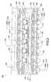
- FIG. 1is a diagrammatic sketch in a sectional view illustrating the structure of an example of a conventional stacked package (i.e. package-on-package, POP) device 50 , i.e. a two-stack multi-package module (MPM), in which the interconnection is made by solder balls 28 .
- POPpackage-on-package
- MPMtwo-stack multi-package module
- a first packageis the “top” package 20
- a second packageis the “bottom” package 10
- the top package 20is stacked on the bottom package 10 .
- the top package 20includes a chip 24 attached onto the substrate 22 .
- the substrate 22 of the top package 20has upper and lower metal layers patterned to provide appropriate circuitry and connected by way of vias.
- the chip 24is attached on an upper surface of the substrate 22 by using an adhesive 23 , e.g. die attach epoxy.
- the bottom package 10includes a chip 14 attached onto a substrate 12 .
- the substrate 12 of the bottom package 10also has upper and lower metal layers patterned to provide appropriate circuitry and connected by way of vias.
- the chip 14is attached on an upper surface of the substrate 12 by using an adhesive 13 , e.g. die attach epoxy.
- the chips 24 , 14are respectively bonded to wire bond sites on the upper metal layer of the substrate 22 , 12 by means of bonding wires 26 , 16 , so as to establish electrical connections.
- the chips 24 , 14 and the bonding wires 26 , 16are respectively encapsulated with top and bottom molding compound 27 , 17 .
- Solder balls 28are mounted onto bonding pads located on the peripheral margin of a lower surface of the substrate 22 to provide interconnection to the bottom package 10 .
- Solder balls 18are mounted onto bonding pads located on a lower surface of the substrate 12 to provide electrical connection to an external circuit board (not shown).
- the interconnection between the top and bottom packages 20 , 10 of the POP device 50is achieved by reflowing the solder balls 28 attached to the bonding pads located on the peripheral margin of the lower surface of the substrate 22 of the top package 20 and attached to the bonding pads located on the peripheral margin of the upper surface of the substrate 12 of the bottom package 10 .
- the conventional POP devicehas not any interposer or substrate which is disposed between the top and bottom packages 20 , 10 for providing the electrical connection or more functions.
- the present inventionprovides a bottom package of a stacked package (i.e. package-on-package, POP) device, which includes a substrate, a chip, an interposer and a molding compound.
- the substratehas an upper surface and a lower surface opposite to the upper surface.
- the chipis electrically connected to the upper surface of the substrate.
- the interposeris disposed on the chip, and electrically connected to the upper surface of the substrate.
- the interposerincludes an embedded component and a plurality of electric contacts, wherein the embedded component is located between the upper and lower surfaces of the interposer, and the electric contacts are located on the upper surface of the interposer.
- the molding compoundseals the chip and covers the upper surface of the substrate and the lower surface of the interposer.
- the interposercan provide the bottom and top packages with electrical connection, and the interposer can provide more functions.
- FIG. 1is a cross-sectional view of a stacked package device in the prior art.
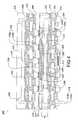
- FIG. 2is cross-sectional view of a stacked package device according to an embodiment of the present invention.
- FIG. 3is cross-sectional view of an interposer according to the embodiment of the present invention.
- FIG. 4is cross-sectional view of a stacked package device according to another embodiment of the present invention.
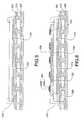
- FIGS. 5 and 9are cross-sectional views showing a method for manufacturing a bottom package of the stacked package device according to the embodiment of the present invention.
- FIG. 2it depicts a stacked package (i.e. package-on-package, POP) device 200 according to an embodiment of the present invention.
- the POP device 200includes a top package 220 and a bottom package 210 .
- the bottom package 210includes a first chip 214 mounted and electrically connected to an upper surface 242 of a first substrate 212 .
- the first substrate 212 of the bottom package 210has upper and lower metal layers which can be patterned to provide appropriate circuitry and electrically connected by way of vias.
- An interposer 230is disposed on the first chip 214 and electrically connected to the upper surface 242 of the first substrate 212 .
- the interposer 230can be a multi-layer circuit substrate or a silicon substrate with circuit formed therein.
- a silicon substrate 130has an upper surface 136 and a lower surface 138 .
- An embedded component 232is disposed within an opening 132 of the silicon substrate 130 and secured by a molding compound material 134 , and is located between the upper and lower surfaces 136 , 138 .
- Circuit layers 142 , 144are formed on the upper and lower surfaces 136 , 138 by a re-distribution layer (RDL) process.
- the silicon substrate 130includes a plurality of through via 140 extended from the upper surface 136 to the lower surface 138 for electrically connecting the circuit layers to each other.
- the interposer 230has an upper surface 236 and a lower surface 238 .
- the lower surface 238is opposite to the upper surface 236 and faces the first chip 214 .
- the interposer 230includes an embedded component 232 and a plurality of electric contacts 234 , wherein the embedded component 232 is located between the upper and lower surfaces 236 , 238 , and the electric contacts 234 are located on the upper surface 236 of the interposer 230 .
- the electric contact 234includes a pad 234 a and a pre-solder 234 b disposed on the pad 234 a.
- the electric contact 234includes a pad 234 a and a solder ball (not shown) disposed on the pad 234 a.
- a plurality of bonding wires 231are adapted to electrically connect the interposer 230 to the upper surface 242 of the first substrate 212 .
- the embedded component 232can be an active component (e.g. chip) or a passive component (e.g. capacitor).
- a first molding compound 217seals the first chip 214 and the bonding wires 231 and covers the upper surface 242 of the first substrate 212 and the lower surface 238 of the interposer 230 .
- the first molding compound 217exposes the lower surface 244 of the first substrate 212 and the electrical contacts 234 of the interposer 230 .
- the top package 220is stacked on the bottom package 210 .
- the top package 220includes a second chip 224 mounted and electrically connected to an upper surface 246 of the second substrate 222 .
- a lower surface 248 of the second substrate 222is electrically connected to the electrical contacts 234 of the interposer 230 .
- the second substrate 222 of the top package 220also has upper and lower metal layers which can be patterned to provide appropriate circuitry and electrically connected by way of vias.
- a second molding compound 227seals the second chip 224 and covers the upper surface 242 of the second substrate 222 .
- the second molding compound 227exposes the lower surface 248 of the second substrate 222 .
- the first and second chips 214 , 224are mounted on the upper surfaces 242 , 246 of the first and second substrates 212 , 222 by adhesives 213 , 214 e.g. die attach epoxy, respectively. Also, the first and second chips 214 , 224 are electrically connected to the upper surfaces 242 , 246 of the first and second substrates 212 , 222 by bonding wires 216 , 226 , respectively. The bonding wires 216 , 226 are also sealed by the first and second molding compounds 217 , 227 , respectively. Or, in an alternative embodiment the first and second chips 214 , 224 are bonded to the upper surfaces 242 , 246 of the first and second substrates 212 , 222 by bumps (not shown), respectively.
- a plurality of electrical contacts 228are formed on the lower surface 248 of the second substrate 222 for electrically connecting to the electrical contacts 234 of the interposer 230 of the bottom package 210 .
- a plurality of electrical contacts 218are formed on the lower surface 244 of the first substrate 212 for electrically connecting to an external circuit board (not shown).
- a spacer 250can be disposed between the first chip 214 and the interposer 230 , when the size of the interposer 230 is greater than that of the first chip 214 , whereby there is a predetermined gap H between the first substrate 212 and the interposer 230 .
- the predetermined gap His greater than the height of the bonding wires 216 so as to prevent the interposer 230 from touching the bonding wires 216 .
- the first molding compound 217can expose the upper surface 236 of the interposer 230 for dissipating the heat of the interposer 230 .
- the electrical contact 234only includes a pad (e.g. ball-shaped pad).
- a third chip 252can be mounted and electrically connected to the lower surface 244 of the first substrate 212 by means of wire bonding process or flip chip bonding process, thereby providing more functions.
- a plurality of electrical contacts 218e.g. the combination of solder balls 218 b and pads 218 a ) are formed on the lower surface 244 of the first substrate 212 , i.e. the solder balls 218 b is disposed on the lower surface 224 of the substrate 212 for electrically connecting to an external circuit board (not shown).
- the interposercan provide the bottom and top packages with electrical connection, and the interposer can provide more functions.
- FIGS. 5 to 9they depict a method for manufacturing the bottom package (e.g. semiconductor package) 210 of the POP device 200 of the embodiment of the prevent invention.
- a substrate 212is provided, wherein the substrate 212 has an upper surface 242 and a lower surface 244 opposite to the upper surface 242 .
- a chip 214can be mounted and electrically connected to the upper surface 242 of the substrate 212 by means of a wire bonding process.
- an interposer 230is disposed on the chip 214 and electrically connected to the substrate 212 , wherein the interposer 230 has an upper surface 236 and a lower surface 238 , and the lower surface 238 is opposite to the upper surface 236 and faces the chip 214 .
- the interposer 230includes an embedded component 232 and a plurality of electric contacts 234 , wherein the embedded component 232 is located between the upper and lower surfaces 236 , 238 , and the electric contacts 234 are located on the upper surface 236 of the interposer 230 .
- the electric contact 234includes a pad 234 a and a pre-solder 234 b disposed on the pad 234 a. Referring to FIG.
- a plurality of bonding wires 231are provided for electrically connecting the interposer 230 to the upper surface 242 of the substrate 212 .
- a molding compound 217is applied or molded on the upper surface 242 of the substrate 212 to seal the chip 214 and the bonding wires 231 and to cover the lower surface 238 of the interposer 230 .
- the molding compound 217exposes the lower surface 244 of the substrate 212 .
- a plurality of via holes 256are formed in the molding compound 217 by a drilling process (e.g. laser drilling process), thereby exposing the electric contacts 234 of the interposer 230 .
- a plurality of solder balls 218 bare mounted on pads 218 a located on the lower surface 248 of the substrate 212 so as to form the bottom package 210 of the prevent invention.
Landscapes
- Engineering & Computer Science (AREA)
- Microelectronics & Electronic Packaging (AREA)
- Power Engineering (AREA)
- Physics & Mathematics (AREA)
- Condensed Matter Physics & Semiconductors (AREA)
- General Physics & Mathematics (AREA)
- Computer Hardware Design (AREA)
- Structures Or Materials For Encapsulating Or Coating Semiconductor Devices Or Solid State Devices (AREA)
Abstract
Description
- This application claims the priority benefit of Taiwan Patent Application Serial Number 097146551, filed on Dec. 1, 2008, the full disclosure of which is incorporated herein by reference.
- 1. Field of the Invention
- The present invention generally relates to a stacked package device, and more particularly to a bottom package of a stacked package device including an interposer.
- 2. Description of the Related Art
- Currently, a package-on-package (hereinafter referred to as POP) device is related to a semiconductor package disposed on another semiconductor package. The basic object of the POP device is to increase the density of components so as to result in more functions of components per unit volume and better regional efficiency. Thus, the total area of the POP device can be decreased, and the cost is reduced simultaneously.
FIG. 1 is a diagrammatic sketch in a sectional view illustrating the structure of an example of a conventional stacked package (i.e. package-on-package, POP)device 50, i.e. a two-stack multi-package module (MPM), in which the interconnection is made bysolder balls 28. In thisPOP device 50, a first package is the “top”package 20, and a second package is the “bottom”package 10. Thetop package 20 is stacked on thebottom package 10. Thetop package 20 includes achip 24 attached onto thesubstrate 22. Thesubstrate 22 of thetop package 20 has upper and lower metal layers patterned to provide appropriate circuitry and connected by way of vias. Thechip 24 is attached on an upper surface of thesubstrate 22 by using anadhesive 23, e.g. die attach epoxy. Thebottom package 10 includes achip 14 attached onto asubstrate 12. Thesubstrate 12 of thebottom package 10 also has upper and lower metal layers patterned to provide appropriate circuitry and connected by way of vias. Thechip 14 is attached on an upper surface of thesubstrate 12 by using anadhesive 13, e.g. die attach epoxy.- In the top and
bottom packages chips substrate bonding wires chips bonding wires bottom molding compound Solder balls 28 are mounted onto bonding pads located on the peripheral margin of a lower surface of thesubstrate 22 to provide interconnection to thebottom package 10.Solder balls 18 are mounted onto bonding pads located on a lower surface of thesubstrate 12 to provide electrical connection to an external circuit board (not shown). - The interconnection between the top and
bottom packages POP device 50 is achieved by reflowing thesolder balls 28 attached to the bonding pads located on the peripheral margin of the lower surface of thesubstrate 22 of thetop package 20 and attached to the bonding pads located on the peripheral margin of the upper surface of thesubstrate 12 of thebottom package 10. - However, the conventional POP device has not any interposer or substrate which is disposed between the top and
bottom packages - Accordingly, there exists a need for a stacked package device capable of solving the above-mentioned problems.
- The present invention provides a bottom package of a stacked package (i.e. package-on-package, POP) device, which includes a substrate, a chip, an interposer and a molding compound. The substrate has an upper surface and a lower surface opposite to the upper surface. The chip is electrically connected to the upper surface of the substrate. The interposer is disposed on the chip, and electrically connected to the upper surface of the substrate. The interposer includes an embedded component and a plurality of electric contacts, wherein the embedded component is located between the upper and lower surfaces of the interposer, and the electric contacts are located on the upper surface of the interposer. The molding compound seals the chip and covers the upper surface of the substrate and the lower surface of the interposer.
- According to the POP device of the embodiment of the prevent invention, the interposer can provide the bottom and top packages with electrical connection, and the interposer can provide more functions.
- The foregoing, as well as additional objects, features and advantages of the invention will be more apparent from the following detailed description, which proceeds with reference to the accompanying drawings.
FIG. 1 is a cross-sectional view of a stacked package device in the prior art.FIG. 2 is cross-sectional view of a stacked package device according to an embodiment of the present invention.FIG. 3 is cross-sectional view of an interposer according to the embodiment of the present invention.FIG. 4 is cross-sectional view of a stacked package device according to another embodiment of the present invention.FIGS. 5 and 9 are cross-sectional views showing a method for manufacturing a bottom package of the stacked package device according to the embodiment of the present invention.- Referring to
FIG. 2 , it depicts a stacked package (i.e. package-on-package, POP)device 200 according to an embodiment of the present invention. ThePOP device 200 includes atop package 220 and abottom package 210. - The
bottom package 210 includes afirst chip 214 mounted and electrically connected to anupper surface 242 of afirst substrate 212. Thefirst substrate 212 of thebottom package 210 has upper and lower metal layers which can be patterned to provide appropriate circuitry and electrically connected by way of vias. Aninterposer 230 is disposed on thefirst chip 214 and electrically connected to theupper surface 242 of thefirst substrate 212. Referring toFIG. 3 , theinterposer 230 can be a multi-layer circuit substrate or a silicon substrate with circuit formed therein. For example, asilicon substrate 130 has anupper surface 136 and alower surface 138. An embeddedcomponent 232 is disposed within anopening 132 of thesilicon substrate 130 and secured by amolding compound material 134, and is located between the upper andlower surfaces Circuit layers lower surfaces silicon substrate 130 includes a plurality of through via140 extended from theupper surface 136 to thelower surface 138 for electrically connecting the circuit layers to each other. Referring toFIG. 2 again, theinterposer 230 has anupper surface 236 and alower surface 238. Thelower surface 238 is opposite to theupper surface 236 and faces thefirst chip 214. Theinterposer 230 includes an embeddedcomponent 232 and a plurality ofelectric contacts 234, wherein the embeddedcomponent 232 is located between the upper andlower surfaces electric contacts 234 are located on theupper surface 236 of theinterposer 230. In this embodiment, theelectric contact 234 includes apad 234aand a pre-solder234bdisposed on thepad 234a.Or, in another embodiment theelectric contact 234 includes apad 234aand a solder ball (not shown) disposed on thepad 234a.A plurality ofbonding wires 231 are adapted to electrically connect theinterposer 230 to theupper surface 242 of thefirst substrate 212. The embeddedcomponent 232 can be an active component (e.g. chip) or a passive component (e.g. capacitor). Afirst molding compound 217 seals thefirst chip 214 and thebonding wires 231 and covers theupper surface 242 of thefirst substrate 212 and thelower surface 238 of theinterposer 230. Thefirst molding compound 217 exposes thelower surface 244 of thefirst substrate 212 and theelectrical contacts 234 of theinterposer 230. - The
top package 220 is stacked on thebottom package 210. Thetop package 220 includes asecond chip 224 mounted and electrically connected to anupper surface 246 of thesecond substrate 222. Alower surface 248 of thesecond substrate 222 is electrically connected to theelectrical contacts 234 of theinterposer 230. Thesecond substrate 222 of thetop package 220 also has upper and lower metal layers which can be patterned to provide appropriate circuitry and electrically connected by way of vias. Asecond molding compound 227 seals thesecond chip 224 and covers theupper surface 242 of thesecond substrate 222. Thesecond molding compound 227 exposes thelower surface 248 of thesecond substrate 222. - According to the
bottom package 210 and thetop package 220, in this embodiment the first andsecond chips upper surfaces second substrates adhesives second chips upper surfaces second substrates wires bonding wires second chips upper surfaces second substrates - Referring to
FIG. 2 again, a plurality of electrical contacts228 (e.g. the combination ofsolder balls 228bandpads 228a) are formed on thelower surface 248 of thesecond substrate 222 for electrically connecting to theelectrical contacts 234 of theinterposer 230 of thebottom package 210. Thus, the interconnection between the top andbottom packages POP device 200 is achieved. A plurality of electrical contacts218 (e.g. the combination ofsolder balls 218bandpads 218a) are formed on thelower surface 244 of thefirst substrate 212 for electrically connecting to an external circuit board (not shown). - Referring to
FIG. 4 , in another embodiment a spacer250 can be disposed between thefirst chip 214 and theinterposer 230, when the size of theinterposer 230 is greater than that of thefirst chip 214, whereby there is a predetermined gap H between thefirst substrate 212 and theinterposer 230. The predetermined gap H is greater than the height of thebonding wires 216 so as to prevent theinterposer 230 from touching thebonding wires 216. Furthermore, thefirst molding compound 217 can expose theupper surface 236 of theinterposer 230 for dissipating the heat of theinterposer 230. Theelectrical contact 234 only includes a pad (e.g. ball-shaped pad). Athird chip 252 can be mounted and electrically connected to thelower surface 244 of thefirst substrate 212 by means of wire bonding process or flip chip bonding process, thereby providing more functions. A plurality of electrical contacts218 (e.g. the combination ofsolder balls 218bandpads 218a) are formed on thelower surface 244 of thefirst substrate 212, i.e. thesolder balls 218bis disposed on thelower surface 224 of thesubstrate 212 for electrically connecting to an external circuit board (not shown). - According to the POP device of the embodiment of the prevent invention, the interposer can provide the bottom and top packages with electrical connection, and the interposer can provide more functions.
- Referring to
FIGS. 5 to 9 , they depict a method for manufacturing the bottom package (e.g. semiconductor package)210 of thePOP device 200 of the embodiment of the prevent invention. Referring toFIG. 5 , asubstrate 212 is provided, wherein thesubstrate 212 has anupper surface 242 and alower surface 244 opposite to theupper surface 242. In this embodiment, achip 214 can be mounted and electrically connected to theupper surface 242 of thesubstrate 212 by means of a wire bonding process. Referring toFIG. 6 , aninterposer 230 is disposed on thechip 214 and electrically connected to thesubstrate 212, wherein theinterposer 230 has anupper surface 236 and alower surface 238, and thelower surface 238 is opposite to theupper surface 236 and faces thechip 214. Theinterposer 230 includes an embeddedcomponent 232 and a plurality ofelectric contacts 234, wherein the embeddedcomponent 232 is located between the upper andlower surfaces electric contacts 234 are located on theupper surface 236 of theinterposer 230. In this embodiment, theelectric contact 234 includes apad 234aand a pre-solder234bdisposed on thepad 234a.Referring toFIG. 7 , a plurality ofbonding wires 231 are provided for electrically connecting theinterposer 230 to theupper surface 242 of thesubstrate 212. Referring toFIG. 8 , amolding compound 217 is applied or molded on theupper surface 242 of thesubstrate 212 to seal thechip 214 and thebonding wires 231 and to cover thelower surface 238 of theinterposer 230. Themolding compound 217 exposes thelower surface 244 of thesubstrate 212. Furthermore, a plurality of viaholes 256 are formed in themolding compound 217 by a drilling process (e.g. laser drilling process), thereby exposing theelectric contacts 234 of theinterposer 230. Referring toFIG. 9 , finally a plurality ofsolder balls 218bare mounted onpads 218alocated on thelower surface 248 of thesubstrate 212 so as to form thebottom package 210 of the prevent invention. - Although the invention has been explained in relation to its preferred embodiment, it is not used to limit the invention. It is to be understood that many other possible modifications and variations can be made by those skilled in the art without departing from the spirit and scope of the invention as hereinafter claimed.
Claims (20)
1. A semiconductor package comprising:
a substrate having an upper surface and a lower surface opposite to the upper surface;
a chip electrically connected to the upper surface of the substrate;
an interposer disposed on the chip and electrically connected to the substrate, wherein the interposer has an upper surface and a lower surface, the lower surface is opposite to the upper surface and faces the chip, the interposer comprises an embedded component and a plurality of first electric contacts, the embedded component is located between the upper and lower surfaces of the interposer, and the first electric contacts are located on the upper surface of the interposer; and
a molding compound sealing the chip and covering the upper surface of the substrate and the lower surface of the interposer.
2. The semiconductor package as claimed inclaim 1 , further comprising:
a plurality of first bonding wires adapted to electrically connect the interposer to the upper surface of the substrate.
3. The semiconductor package as claimed inclaim 1 , further comprising:
a plurality of second bonding wires adapted to electrically connect the chip to the substrate.
4. The semiconductor package as claimed inclaim 3 , further comprising:
a spacer disposed between the chip and the interposer, whereby there is a predetermined gap between the substrate and the interposer, wherein the predetermined gap is greater than the height of the second bonding wires.
5. The semiconductor package as claimed inclaim 4 , wherein the size of the interposer is greater than that of the chip.
6. The semiconductor package as claimed inclaim 1 , wherein the interposer is one of a multi-layer circuit substrate and a silicon substrate with circuit formed therein.
7. The semiconductor package as claimed inclaim 1 , wherein the embedded component is an active component.
8. The semiconductor package as claimed inclaim 1 , wherein the embedded component is a passive component.
9. The semiconductor package as claimed inclaim 1 , wherein the first electric contact comprises a pad.
10. The semiconductor package as claimed inclaim 9 , wherein the first electric contact further comprises a pre-solder disposed on the pad.
11. The semiconductor package as claimed inclaim 9 , wherein the first electric contact further comprises a first solder ball disposed on the pad.
12. The semiconductor package as claimed inclaim 3 , further comprising:
another chip mounted and electrically connected to the lower surface of the substrate; and
a plurality of second solder balls disposed on the lower surface of the substrate, wherein the another chip is surrounded by the second solder balls.
13. The semiconductor package as claimed inclaim 1 , wherein the molding compound exposes the upper surface of the interposer.
14. The semiconductor package as claimed inclaim 1 , wherein the molding compound exposes the first electric contacts of the interposer.
15. The semiconductor package as claimed inclaim 14 , wherein the molding compound comprises a plurality of via holes, the via holes exposing the first electric contacts of the interposer.
16. A method for manufacturing a semiconductor package comprising the following steps of:
providing a substrate, wherein the substrate has an upper surface and a lower surface opposite to the upper surface;
electrically connecting a chip to the upper surface of the substrate;
disposing an interposer on the chip and electrically connecting the interposer to the substrate, wherein the interposer has an upper surface and a lower surface, the lower surface is opposite to the upper surface and faces the chip, the interposer comprises an embedded component and a plurality of electric contacts, the embedded component is located between the upper and lower surfaces, and the electric contacts are located on the upper surface of the interposer; and
applying a molding compound on the upper surface of the substrate to seal the chip and cover the lower surface of the interposer.
17. The method as claimed inclaim 16 , further comprises the following step:
forming a plurality of via holes in the molding compound, the via holes exposing the electric contacts of the interpose.
18. A stacked package device comprising:
a bottom package comprising:
a first substrate having an upper surface and a lower surface opposite to the upper surface;
a first chip electrically connected to the first substrate;
an interposer disposed on the first chip and electrically connected to the first substrate, wherein the interposer has an upper surface and a lower surface, the lower surface is opposite to the upper surface and faces the first chip, the interposer comprises an embedded component and a plurality of first electric contacts, the embedded component is located between the upper and lower surfaces, and the first electric contacts are located on the upper surface of the interposer; and
a first molding compound sealing the first chip and covering the upper surface of the first substrate and the lower surface of the interposer; and
a top package stacked on the bottom package and comprising:
a second substrate having an upper surface and a lower surface, wherein the lower surface is opposite to the upper surface and electrically connecting to the first electric contacts of the interposer;
a second chip electrically connected to the second substrate; and
a second molding compound sealing the second chip and covering the upper surface of the substrate.
19. The stacked package device as claimed inclaim 18 , wherein the second substrate comprises a plurality of second electrical contacts formed on the lower surface of the second substrate and electrically connected to the first electrical contacts respectively.
20. The stacked package device as claimed inclaim 18 , wherein the interposer is one of a multi-layer circuit substrate and a silicon substrate with circuit formed therein.
Applications Claiming Priority (3)
| Application Number | Priority Date | Filing Date | Title |
|---|---|---|---|
| TW97146551A | 2008-12-01 | ||
| TW097146551ATW201023308A (en) | 2008-12-01 | 2008-12-01 | Package-on-package device, semiconductor package and method for manufacturing the same |
| TW097146551 | 2008-12-01 |
Publications (2)
| Publication Number | Publication Date |
|---|---|
| US20100133675A1true US20100133675A1 (en) | 2010-06-03 |
| US7838334B2 US7838334B2 (en) | 2010-11-23 |
Family
ID=42222014
Family Applications (1)
| Application Number | Title | Priority Date | Filing Date |
|---|---|---|---|
| US12/565,501ActiveUS7838334B2 (en) | 2008-12-01 | 2009-09-23 | Package-on-package device, semiconductor package and method for manufacturing the same |
Country Status (2)
| Country | Link |
|---|---|
| US (1) | US7838334B2 (en) |
| TW (1) | TW201023308A (en) |
Cited By (47)
| Publication number | Priority date | Publication date | Assignee | Title |
|---|---|---|---|---|
| US20120001315A1 (en)* | 2010-06-30 | 2012-01-05 | Hitachi, Ltd. | Semiconductor device |
| US20120319265A1 (en)* | 2011-06-16 | 2012-12-20 | In Sang Yoon | Integrated circuit packaging system with molded laser via interposer and method of manufacture thereof |
| US20130105979A1 (en)* | 2011-10-31 | 2013-05-02 | Taiwan Semiconductor Manufacturing Company, Ltd. | Package on Package Devices and Methods of Packaging Semiconductor Dies |
| US8482111B2 (en) | 2010-07-19 | 2013-07-09 | Tessera, Inc. | Stackable molded microelectronic packages |
| US8525314B2 (en) | 2004-11-03 | 2013-09-03 | Tessera, Inc. | Stacked packaging improvements |
| US8618654B2 (en)* | 2010-07-20 | 2013-12-31 | Marvell World Trade Ltd. | Structures embedded within core material and methods of manufacturing thereof |
| US8618659B2 (en) | 2011-05-03 | 2013-12-31 | Tessera, Inc. | Package-on-package assembly with wire bonds to encapsulation surface |
| US8623706B2 (en) | 2010-11-15 | 2014-01-07 | Tessera, Inc. | Microelectronic package with terminals on dielectric mass |
| US20140077363A1 (en)* | 2012-09-14 | 2014-03-20 | Stats Chippac, Ltd. | Semiconductor Device and Method of Forming Dual-Sided Interconnect Structures in Fo-WLCSP |
| US8728865B2 (en) | 2005-12-23 | 2014-05-20 | Tessera, Inc. | Microelectronic packages and methods therefor |
| US8835228B2 (en) | 2012-05-22 | 2014-09-16 | Invensas Corporation | Substrate-less stackable package with wire-bond interconnect |
| US8836136B2 (en) | 2011-10-17 | 2014-09-16 | Invensas Corporation | Package-on-package assembly with wire bond vias |
| US8878353B2 (en) | 2012-12-20 | 2014-11-04 | Invensas Corporation | Structure for microelectronic packaging with bond elements to encapsulation surface |
| US8883563B1 (en) | 2013-07-15 | 2014-11-11 | Invensas Corporation | Fabrication of microelectronic assemblies having stack terminals coupled by connectors extending through encapsulation |
| US8975738B2 (en) | 2012-11-12 | 2015-03-10 | Invensas Corporation | Structure for microelectronic packaging with terminals on dielectric mass |
| US9023691B2 (en) | 2013-07-15 | 2015-05-05 | Invensas Corporation | Microelectronic assemblies with stack terminals coupled by connectors extending through encapsulation |
| US9034696B2 (en) | 2013-07-15 | 2015-05-19 | Invensas Corporation | Microelectronic assemblies having reinforcing collars on connectors extending through encapsulation |
| US20150155243A1 (en)* | 2013-12-04 | 2015-06-04 | Taiwan Semiconductor Manufacturing Company, Ltd. | Warpage Control in Package-on-Package Structures |
| US9076749B2 (en)* | 2013-10-15 | 2015-07-07 | Stmicroelectronics (Grenoble 2) Sas | Electronic system comprising stacked electronic devices comprising integrated-circuit chips |
| US9082753B2 (en) | 2013-11-12 | 2015-07-14 | Invensas Corporation | Severing bond wire by kinking and twisting |
| US9087815B2 (en) | 2013-11-12 | 2015-07-21 | Invensas Corporation | Off substrate kinking of bond wire |
| US9171790B2 (en) | 2012-05-30 | 2015-10-27 | Taiwan Semiconductor Manufacturing Company, Ltd. | Package on package devices and methods of packaging semiconductor dies |
| US9214454B2 (en) | 2014-03-31 | 2015-12-15 | Invensas Corporation | Batch process fabrication of package-on-package microelectronic assemblies |
| US9224717B2 (en) | 2011-05-03 | 2015-12-29 | Tessera, Inc. | Package-on-package assembly with wire bonds to encapsulation surface |
| US9324681B2 (en) | 2010-12-13 | 2016-04-26 | Tessera, Inc. | Pin attachment |
| US9349706B2 (en) | 2012-02-24 | 2016-05-24 | Invensas Corporation | Method for package-on-package assembly with wire bonds to encapsulation surface |
| US9391008B2 (en) | 2012-07-31 | 2016-07-12 | Invensas Corporation | Reconstituted wafer-level package DRAM |
| US9412714B2 (en) | 2014-05-30 | 2016-08-09 | Invensas Corporation | Wire bond support structure and microelectronic package including wire bonds therefrom |
| US20160284631A1 (en)* | 2015-03-27 | 2016-09-29 | Fairchild Semiconductor Corporation | Substrate interposer on a leadframe |
| US9502390B2 (en) | 2012-08-03 | 2016-11-22 | Invensas Corporation | BVA interposer |
| US9553076B2 (en) | 2010-07-19 | 2017-01-24 | Tessera, Inc. | Stackable molded microelectronic packages with area array unit connectors |
| US20170040304A1 (en)* | 2015-08-03 | 2017-02-09 | Siliconware Precision Industries Co., Ltd. | Electronic package and fabrication method thereof |
| US9583411B2 (en) | 2014-01-17 | 2017-02-28 | Invensas Corporation | Fine pitch BVA using reconstituted wafer with area array accessible for testing |
| US9601454B2 (en) | 2013-02-01 | 2017-03-21 | Invensas Corporation | Method of forming a component having wire bonds and a stiffening layer |
| US9646917B2 (en) | 2014-05-29 | 2017-05-09 | Invensas Corporation | Low CTE component with wire bond interconnects |
| US9659848B1 (en) | 2015-11-18 | 2017-05-23 | Invensas Corporation | Stiffened wires for offset BVA |
| US9685365B2 (en) | 2013-08-08 | 2017-06-20 | Invensas Corporation | Method of forming a wire bond having a free end |
| US9691679B2 (en) | 2012-02-24 | 2017-06-27 | Invensas Corporation | Method for package-on-package assembly with wire bonds to encapsulation surface |
| US9728527B2 (en) | 2013-11-22 | 2017-08-08 | Invensas Corporation | Multiple bond via arrays of different wire heights on a same substrate |
| US9852969B2 (en) | 2013-11-22 | 2017-12-26 | Invensas Corporation | Die stacks with one or more bond via arrays of wire bond wires and with one or more arrays of bump interconnects |
| US10008477B2 (en) | 2013-09-16 | 2018-06-26 | Invensas Corporation | Microelectronic element with bond elements to encapsulation surface |
| US10026717B2 (en) | 2013-11-22 | 2018-07-17 | Invensas Corporation | Multiple bond via arrays of different wire heights on a same substrate |
| US20180226366A1 (en)* | 2017-02-03 | 2018-08-09 | Samsung Electro-Mechanics Co., Ltd. | Semiconductor package and manufacturing method thereof |
| CN109904127A (en)* | 2015-06-16 | 2019-06-18 | 合肥矽迈微电子科技有限公司 | Packaging structure and packaging method |
| US10332854B2 (en) | 2015-10-23 | 2019-06-25 | Invensas Corporation | Anchoring structure of fine pitch bva |
| US10460958B2 (en) | 2013-08-07 | 2019-10-29 | Invensas Corporation | Method of manufacturing embedded packaging with preformed vias |
| US20220139812A1 (en)* | 2020-11-03 | 2022-05-05 | Advanced Semiconductor Engineering, Inc. | Semiconductor package structure and method for manufacturing the same |
Families Citing this family (38)
| Publication number | Priority date | Publication date | Assignee | Title |
|---|---|---|---|---|
| TWI335070B (en)* | 2007-03-23 | 2010-12-21 | Advanced Semiconductor Eng | Semiconductor package and the method of making the same |
| TWI473553B (en) | 2008-07-03 | 2015-02-11 | Advanced Semiconductor Eng | Chip package structure |
| US8012797B2 (en)* | 2009-01-07 | 2011-09-06 | Advanced Semiconductor Engineering, Inc. | Method for forming stackable semiconductor device packages including openings with conductive bumps of specified geometries |
| TWI499024B (en)* | 2009-01-07 | 2015-09-01 | Advanced Semiconductor Eng | Package-on-package device, semiconductor package and method for manufacturing the same |
| US20100171206A1 (en)* | 2009-01-07 | 2010-07-08 | Chi-Chih Chu | Package-on-Package Device, Semiconductor Package, and Method for Manufacturing The Same |
| US8198131B2 (en) | 2009-11-18 | 2012-06-12 | Advanced Semiconductor Engineering, Inc. | Stackable semiconductor device packages |
| TWI408785B (en) | 2009-12-31 | 2013-09-11 | Advanced Semiconductor Eng | Semiconductor package |
| US8569894B2 (en) | 2010-01-13 | 2013-10-29 | Advanced Semiconductor Engineering, Inc. | Semiconductor package with single sided substrate design and manufacturing methods thereof |
| TWI419283B (en) | 2010-02-10 | 2013-12-11 | Advanced Semiconductor Eng | Package structure |
| TWI411075B (en) | 2010-03-22 | 2013-10-01 | Advanced Semiconductor Eng | Semiconductor package and manufacturing method thereof |
| US8278746B2 (en) | 2010-04-02 | 2012-10-02 | Advanced Semiconductor Engineering, Inc. | Semiconductor device packages including connecting elements |
| US8624374B2 (en) | 2010-04-02 | 2014-01-07 | Advanced Semiconductor Engineering, Inc. | Semiconductor device packages with fan-out and with connecting elements for stacking and manufacturing methods thereof |
| TWI451546B (en) | 2010-10-29 | 2014-09-01 | Advanced Semiconductor Eng | Stacked semiconductor package, semiconductor package thereof and method for making a semiconductor package |
| TWI445155B (en) | 2011-01-06 | 2014-07-11 | Advanced Semiconductor Eng | Stacked semiconductor package and method for making the same |
| KR101828386B1 (en)* | 2011-02-15 | 2018-02-13 | 삼성전자주식회사 | Stacked package and method of manufacturing the same |
| US9171792B2 (en) | 2011-02-28 | 2015-10-27 | Advanced Semiconductor Engineering, Inc. | Semiconductor device packages having a side-by-side device arrangement and stacking functionality |
| US8946757B2 (en) | 2012-02-17 | 2015-02-03 | Invensas Corporation | Heat spreading substrate with embedded interconnects |
| US10381326B2 (en) | 2014-05-28 | 2019-08-13 | Invensas Corporation | Structure and method for integrated circuits packaging with increased density |
| KR102243285B1 (en) | 2014-07-01 | 2021-04-23 | 삼성전자주식회사 | A semiconductor package |
| KR102198858B1 (en) | 2014-07-24 | 2021-01-05 | 삼성전자 주식회사 | Semiconductor package stack structure having interposer substrate |
| US9735084B2 (en) | 2014-12-11 | 2017-08-15 | Invensas Corporation | Bond via array for thermal conductivity |
| US9888579B2 (en) | 2015-03-05 | 2018-02-06 | Invensas Corporation | Pressing of wire bond wire tips to provide bent-over tips |
| US9502372B1 (en) | 2015-04-30 | 2016-11-22 | Invensas Corporation | Wafer-level packaging using wire bond wires in place of a redistribution layer |
| US9761554B2 (en) | 2015-05-07 | 2017-09-12 | Invensas Corporation | Ball bonding metal wire bond wires to metal pads |
| US9490222B1 (en) | 2015-10-12 | 2016-11-08 | Invensas Corporation | Wire bond wires for interference shielding |
| US10490528B2 (en) | 2015-10-12 | 2019-11-26 | Invensas Corporation | Embedded wire bond wires |
| US10181457B2 (en) | 2015-10-26 | 2019-01-15 | Invensas Corporation | Microelectronic package for wafer-level chip scale packaging with fan-out |
| KR101933408B1 (en) | 2015-11-10 | 2018-12-28 | 삼성전기 주식회사 | Electronic component package and electronic device comprising the same |
| US10043779B2 (en) | 2015-11-17 | 2018-08-07 | Invensas Corporation | Packaged microelectronic device for a package-on-package device |
| US9984992B2 (en) | 2015-12-30 | 2018-05-29 | Invensas Corporation | Embedded wire bond wires for vertical integration with separate surface mount and wire bond mounting surfaces |
| CN109075151B (en) | 2016-04-26 | 2023-06-27 | 亚德诺半导体国际无限责任公司 | Lead frame for mechanical mating, and electrical and thermal conduction of component package circuits |
| US9935075B2 (en) | 2016-07-29 | 2018-04-03 | Invensas Corporation | Wire bonding method and apparatus for electromagnetic interference shielding |
| US20180114786A1 (en) | 2016-10-21 | 2018-04-26 | Powertech Technology Inc. | Method of forming package-on-package structure |
| US10299368B2 (en) | 2016-12-21 | 2019-05-21 | Invensas Corporation | Surface integrated waveguides and circuit structures therefor |
| US10497635B2 (en) | 2018-03-27 | 2019-12-03 | Linear Technology Holding Llc | Stacked circuit package with molded base having laser drilled openings for upper package |
| US11075151B2 (en)* | 2018-06-29 | 2021-07-27 | Taiwan Semiconductor Manufacturing Company, Ltd. | Fan-out package with controllable standoff |
| US11410977B2 (en) | 2018-11-13 | 2022-08-09 | Analog Devices International Unlimited Company | Electronic module for high power applications |
| US11844178B2 (en) | 2020-06-02 | 2023-12-12 | Analog Devices International Unlimited Company | Electronic component |
Citations (5)
| Publication number | Priority date | Publication date | Assignee | Title |
|---|---|---|---|---|
| US20030205826A1 (en)* | 2000-05-19 | 2003-11-06 | Megic Corporation | Multiple chips bonded to packaging structure with low noise and multiple selectable functions |
| US20060244157A1 (en)* | 2005-04-29 | 2006-11-02 | Flynn Carson | Stacked integrated circuit package system |
| US20090236718A1 (en)* | 2008-03-19 | 2009-09-24 | Joungin Yang | Package-on-package system with internal stacking module interposer |
| US20090236735A1 (en)* | 2008-03-19 | 2009-09-24 | Micron Technology, Inc. | Upgradeable and repairable semiconductor packages and methods |
| US20100038772A1 (en)* | 2008-08-12 | 2010-02-18 | Shinko Electric Industries Co., Ltd. | Semiconductor package and manufacturing method thereof |
- 2008
- 2008-12-01TWTW097146551Apatent/TW201023308A/enunknown
- 2009
- 2009-09-23USUS12/565,501patent/US7838334B2/enactiveActive
Patent Citations (5)
| Publication number | Priority date | Publication date | Assignee | Title |
|---|---|---|---|---|
| US20030205826A1 (en)* | 2000-05-19 | 2003-11-06 | Megic Corporation | Multiple chips bonded to packaging structure with low noise and multiple selectable functions |
| US20060244157A1 (en)* | 2005-04-29 | 2006-11-02 | Flynn Carson | Stacked integrated circuit package system |
| US20090236718A1 (en)* | 2008-03-19 | 2009-09-24 | Joungin Yang | Package-on-package system with internal stacking module interposer |
| US20090236735A1 (en)* | 2008-03-19 | 2009-09-24 | Micron Technology, Inc. | Upgradeable and repairable semiconductor packages and methods |
| US20100038772A1 (en)* | 2008-08-12 | 2010-02-18 | Shinko Electric Industries Co., Ltd. | Semiconductor package and manufacturing method thereof |
Cited By (109)
| Publication number | Priority date | Publication date | Assignee | Title |
|---|---|---|---|---|
| US8525314B2 (en) | 2004-11-03 | 2013-09-03 | Tessera, Inc. | Stacked packaging improvements |
| US9570416B2 (en) | 2004-11-03 | 2017-02-14 | Tessera, Inc. | Stacked packaging improvements |
| US9153562B2 (en) | 2004-11-03 | 2015-10-06 | Tessera, Inc. | Stacked packaging improvements |
| US8927337B2 (en) | 2004-11-03 | 2015-01-06 | Tessera, Inc. | Stacked packaging improvements |
| US8531020B2 (en) | 2004-11-03 | 2013-09-10 | Tessera, Inc. | Stacked packaging improvements |
| US9218988B2 (en) | 2005-12-23 | 2015-12-22 | Tessera, Inc. | Microelectronic packages and methods therefor |
| US9984901B2 (en) | 2005-12-23 | 2018-05-29 | Tessera, Inc. | Method for making a microelectronic assembly having conductive elements |
| US8728865B2 (en) | 2005-12-23 | 2014-05-20 | Tessera, Inc. | Microelectronic packages and methods therefor |
| US9087835B2 (en) | 2010-03-18 | 2015-07-21 | Marvell World Trade Ltd. | Structures embedded within core material and methods of manufacturing thereof |
| US8441115B2 (en)* | 2010-06-30 | 2013-05-14 | Hitachi, Ltd. | Semiconductor device with exposed thermal conductivity part |
| US20120001315A1 (en)* | 2010-06-30 | 2012-01-05 | Hitachi, Ltd. | Semiconductor device |
| US8907466B2 (en) | 2010-07-19 | 2014-12-09 | Tessera, Inc. | Stackable molded microelectronic packages |
| US8482111B2 (en) | 2010-07-19 | 2013-07-09 | Tessera, Inc. | Stackable molded microelectronic packages |
| US10128216B2 (en) | 2010-07-19 | 2018-11-13 | Tessera, Inc. | Stackable molded microelectronic packages |
| US9123664B2 (en) | 2010-07-19 | 2015-09-01 | Tessera, Inc. | Stackable molded microelectronic packages |
| US9570382B2 (en) | 2010-07-19 | 2017-02-14 | Tessera, Inc. | Stackable molded microelectronic packages |
| US9553076B2 (en) | 2010-07-19 | 2017-01-24 | Tessera, Inc. | Stackable molded microelectronic packages with area array unit connectors |
| US8618654B2 (en)* | 2010-07-20 | 2013-12-31 | Marvell World Trade Ltd. | Structures embedded within core material and methods of manufacturing thereof |
| US8637991B2 (en) | 2010-11-15 | 2014-01-28 | Tessera, Inc. | Microelectronic package with terminals on dielectric mass |
| US8957527B2 (en) | 2010-11-15 | 2015-02-17 | Tessera, Inc. | Microelectronic package with terminals on dielectric mass |
| US8659164B2 (en) | 2010-11-15 | 2014-02-25 | Tessera, Inc. | Microelectronic package with terminals on dielectric mass |
| US8623706B2 (en) | 2010-11-15 | 2014-01-07 | Tessera, Inc. | Microelectronic package with terminals on dielectric mass |
| US9324681B2 (en) | 2010-12-13 | 2016-04-26 | Tessera, Inc. | Pin attachment |
| US9224717B2 (en) | 2011-05-03 | 2015-12-29 | Tessera, Inc. | Package-on-package assembly with wire bonds to encapsulation surface |
| US9691731B2 (en) | 2011-05-03 | 2017-06-27 | Tessera, Inc. | Package-on-package assembly with wire bonds to encapsulation surface |
| US11424211B2 (en) | 2011-05-03 | 2022-08-23 | Tessera Llc | Package-on-package assembly with wire bonds to encapsulation surface |
| US9093435B2 (en) | 2011-05-03 | 2015-07-28 | Tessera, Inc. | Package-on-package assembly with wire bonds to encapsulation surface |
| US8618659B2 (en) | 2011-05-03 | 2013-12-31 | Tessera, Inc. | Package-on-package assembly with wire bonds to encapsulation surface |
| US20120319265A1 (en)* | 2011-06-16 | 2012-12-20 | In Sang Yoon | Integrated circuit packaging system with molded laser via interposer and method of manufacture thereof |
| US10083903B1 (en)* | 2011-06-16 | 2018-09-25 | STATS ChipPAC Pte. Ltd. | Integrated circuit packaging system with molded laser via interposer and method of manufacture thereof |
| US8765525B2 (en)* | 2011-06-16 | 2014-07-01 | Stats Chippac Ltd. | Method of manufacturing an integrated circuit packaging system including lasering through encapsulant over interposer |
| US9385066B1 (en)* | 2011-06-16 | 2016-07-05 | STATS ChipPAC Pte. Ltd. | Integrated circuit packaging system with molded laser via interposer and method of manufacture thereof |
| US9252122B2 (en) | 2011-10-17 | 2016-02-02 | Invensas Corporation | Package-on-package assembly with wire bond vias |
| US9041227B2 (en) | 2011-10-17 | 2015-05-26 | Invensas Corporation | Package-on-package assembly with wire bond vias |
| US9761558B2 (en) | 2011-10-17 | 2017-09-12 | Invensas Corporation | Package-on-package assembly with wire bond vias |
| US8836136B2 (en) | 2011-10-17 | 2014-09-16 | Invensas Corporation | Package-on-package assembly with wire bond vias |
| US9105483B2 (en) | 2011-10-17 | 2015-08-11 | Invensas Corporation | Package-on-package assembly with wire bond vias |
| US10756049B2 (en) | 2011-10-17 | 2020-08-25 | Invensas Corporation | Package-on-package assembly with wire bond vias |
| US11189595B2 (en) | 2011-10-17 | 2021-11-30 | Invensas Corporation | Package-on-package assembly with wire bond vias |
| US11735563B2 (en) | 2011-10-17 | 2023-08-22 | Invensas Llc | Package-on-package assembly with wire bond vias |
| US9105552B2 (en)* | 2011-10-31 | 2015-08-11 | Taiwan Semiconductor Manufacturing Company, Ltd. | Package on package devices and methods of packaging semiconductor dies |
| CN103094260A (en)* | 2011-10-31 | 2013-05-08 | 台湾积体电路制造股份有限公司 | Package On Package Devices And Methods Of Packaging Semiconductor Dies |
| USRE49045E1 (en)* | 2011-10-31 | 2022-04-19 | Taiwan Semiconductor Manufacturing Company, Ltd. | Package on package devices and methods of packaging semiconductor dies |
| US20130105979A1 (en)* | 2011-10-31 | 2013-05-02 | Taiwan Semiconductor Manufacturing Company, Ltd. | Package on Package Devices and Methods of Packaging Semiconductor Dies |
| US9349706B2 (en) | 2012-02-24 | 2016-05-24 | Invensas Corporation | Method for package-on-package assembly with wire bonds to encapsulation surface |
| US9691679B2 (en) | 2012-02-24 | 2017-06-27 | Invensas Corporation | Method for package-on-package assembly with wire bonds to encapsulation surface |
| US9953914B2 (en) | 2012-05-22 | 2018-04-24 | Invensas Corporation | Substrate-less stackable package with wire-bond interconnect |
| US8835228B2 (en) | 2012-05-22 | 2014-09-16 | Invensas Corporation | Substrate-less stackable package with wire-bond interconnect |
| US10020286B2 (en) | 2012-05-30 | 2018-07-10 | Taiwan Semiconductor Manufacturing Company, Ltd. | Package on package devices and methods of packaging semiconductor dies |
| US9171790B2 (en) | 2012-05-30 | 2015-10-27 | Taiwan Semiconductor Manufacturing Company, Ltd. | Package on package devices and methods of packaging semiconductor dies |
| US9391008B2 (en) | 2012-07-31 | 2016-07-12 | Invensas Corporation | Reconstituted wafer-level package DRAM |
| US9917073B2 (en) | 2012-07-31 | 2018-03-13 | Invensas Corporation | Reconstituted wafer-level package dram with conductive interconnects formed in encapsulant at periphery of the package |
| US10297582B2 (en) | 2012-08-03 | 2019-05-21 | Invensas Corporation | BVA interposer |
| US9502390B2 (en) | 2012-08-03 | 2016-11-22 | Invensas Corporation | BVA interposer |
| US10192796B2 (en) | 2012-09-14 | 2019-01-29 | STATS ChipPAC Pte. Ltd. | Semiconductor device and method of forming dual-sided interconnect structures in FO-WLCSP |
| US20140077363A1 (en)* | 2012-09-14 | 2014-03-20 | Stats Chippac, Ltd. | Semiconductor Device and Method of Forming Dual-Sided Interconnect Structures in Fo-WLCSP |
| US9978654B2 (en)* | 2012-09-14 | 2018-05-22 | STATS ChipPAC Pte. Ltd. | Semiconductor device and method of forming dual-sided interconnect structures in Fo-WLCSP |
| US11569136B2 (en) | 2012-09-14 | 2023-01-31 | STATS ChipPAC Pte. Ltd. | Semiconductor device and method of forming dual-sided interconnect structures in FO-WLCSP |
| US8975738B2 (en) | 2012-11-12 | 2015-03-10 | Invensas Corporation | Structure for microelectronic packaging with terminals on dielectric mass |
| US9095074B2 (en) | 2012-12-20 | 2015-07-28 | Invensas Corporation | Structure for microelectronic packaging with bond elements to encapsulation surface |
| US8878353B2 (en) | 2012-12-20 | 2014-11-04 | Invensas Corporation | Structure for microelectronic packaging with bond elements to encapsulation surface |
| US9615456B2 (en) | 2012-12-20 | 2017-04-04 | Invensas Corporation | Microelectronic assembly for microelectronic packaging with bond elements to encapsulation surface |
| US9601454B2 (en) | 2013-02-01 | 2017-03-21 | Invensas Corporation | Method of forming a component having wire bonds and a stiffening layer |
| US9633979B2 (en) | 2013-07-15 | 2017-04-25 | Invensas Corporation | Microelectronic assemblies having stack terminals coupled by connectors extending through encapsulation |
| US9034696B2 (en) | 2013-07-15 | 2015-05-19 | Invensas Corporation | Microelectronic assemblies having reinforcing collars on connectors extending through encapsulation |
| US9023691B2 (en) | 2013-07-15 | 2015-05-05 | Invensas Corporation | Microelectronic assemblies with stack terminals coupled by connectors extending through encapsulation |
| US8883563B1 (en) | 2013-07-15 | 2014-11-11 | Invensas Corporation | Fabrication of microelectronic assemblies having stack terminals coupled by connectors extending through encapsulation |
| US10460958B2 (en) | 2013-08-07 | 2019-10-29 | Invensas Corporation | Method of manufacturing embedded packaging with preformed vias |
| US9685365B2 (en) | 2013-08-08 | 2017-06-20 | Invensas Corporation | Method of forming a wire bond having a free end |
| US10008477B2 (en) | 2013-09-16 | 2018-06-26 | Invensas Corporation | Microelectronic element with bond elements to encapsulation surface |
| US9076749B2 (en)* | 2013-10-15 | 2015-07-07 | Stmicroelectronics (Grenoble 2) Sas | Electronic system comprising stacked electronic devices comprising integrated-circuit chips |
| US9893033B2 (en) | 2013-11-12 | 2018-02-13 | Invensas Corporation | Off substrate kinking of bond wire |
| US9082753B2 (en) | 2013-11-12 | 2015-07-14 | Invensas Corporation | Severing bond wire by kinking and twisting |
| US9087815B2 (en) | 2013-11-12 | 2015-07-21 | Invensas Corporation | Off substrate kinking of bond wire |
| US9852969B2 (en) | 2013-11-22 | 2017-12-26 | Invensas Corporation | Die stacks with one or more bond via arrays of wire bond wires and with one or more arrays of bump interconnects |
| US10026717B2 (en) | 2013-11-22 | 2018-07-17 | Invensas Corporation | Multiple bond via arrays of different wire heights on a same substrate |
| US9728527B2 (en) | 2013-11-22 | 2017-08-08 | Invensas Corporation | Multiple bond via arrays of different wire heights on a same substrate |
| US9559064B2 (en)* | 2013-12-04 | 2017-01-31 | Taiwan Semiconductor Manufacturing Company, Ltd. | Warpage control in package-on-package structures |
| US9941221B2 (en) | 2013-12-04 | 2018-04-10 | Taiwan Semiconductor Manufacturing Company, Ltd. | Warpage control in package-on-package structures |
| US20150155243A1 (en)* | 2013-12-04 | 2015-06-04 | Taiwan Semiconductor Manufacturing Company, Ltd. | Warpage Control in Package-on-Package Structures |
| US10170434B2 (en) | 2013-12-04 | 2019-01-01 | Taiwan Semiconductor Manufacturing Company, Ltd. | Warpage control in package-on-package structures |
| US10535616B2 (en) | 2013-12-04 | 2020-01-14 | Taiwan Semiconductor Manufacturing Company, Ltd. | Warpage control in package-on-package structures |
| US9837330B2 (en) | 2014-01-17 | 2017-12-05 | Invensas Corporation | Fine pitch BVA using reconstituted wafer with area array accessible for testing |
| US10529636B2 (en) | 2014-01-17 | 2020-01-07 | Invensas Corporation | Fine pitch BVA using reconstituted wafer with area array accessible for testing |
| US11990382B2 (en) | 2014-01-17 | 2024-05-21 | Adeia Semiconductor Technologies Llc | Fine pitch BVA using reconstituted wafer with area array accessible for testing |
| US9583411B2 (en) | 2014-01-17 | 2017-02-28 | Invensas Corporation | Fine pitch BVA using reconstituted wafer with area array accessible for testing |
| US11404338B2 (en) | 2014-01-17 | 2022-08-02 | Invensas Corporation | Fine pitch bva using reconstituted wafer with area array accessible for testing |
| US9812433B2 (en) | 2014-03-31 | 2017-11-07 | Invensas Corporation | Batch process fabrication of package-on-package microelectronic assemblies |
| US9214454B2 (en) | 2014-03-31 | 2015-12-15 | Invensas Corporation | Batch process fabrication of package-on-package microelectronic assemblies |
| US9356006B2 (en) | 2014-03-31 | 2016-05-31 | Invensas Corporation | Batch process fabrication of package-on-package microelectronic assemblies |
| US9646917B2 (en) | 2014-05-29 | 2017-05-09 | Invensas Corporation | Low CTE component with wire bond interconnects |
| US10475726B2 (en) | 2014-05-29 | 2019-11-12 | Invensas Corporation | Low CTE component with wire bond interconnects |
| US10032647B2 (en) | 2014-05-29 | 2018-07-24 | Invensas Corporation | Low CTE component with wire bond interconnects |
| US9412714B2 (en) | 2014-05-30 | 2016-08-09 | Invensas Corporation | Wire bond support structure and microelectronic package including wire bonds therefrom |
| US20160284631A1 (en)* | 2015-03-27 | 2016-09-29 | Fairchild Semiconductor Corporation | Substrate interposer on a leadframe |
| TWI702701B (en)* | 2015-03-27 | 2020-08-21 | 美商菲爾卻德半導體公司 | Semiconductor device with substrate interposer on a leadframe and method of forming the same |
| CN106024643A (en)* | 2015-03-27 | 2016-10-12 | 费查尔德半导体有限公司 | Substrate interposer on a leadframe |
| US11296069B2 (en)* | 2015-03-27 | 2022-04-05 | Semiconductor Components Industries, Llc | Substrate interposer on a leaderframe |
| US10546847B2 (en)* | 2015-03-27 | 2020-01-28 | Fairchild Semiconductor Corporation | Substrate interposer on a leadframe |
| CN109904127A (en)* | 2015-06-16 | 2019-06-18 | 合肥矽迈微电子科技有限公司 | Packaging structure and packaging method |
| US20190115330A1 (en)* | 2015-08-03 | 2019-04-18 | Siliconware Precision Industries Co., Ltd. | Method for fabricating electronic package |
| US10566320B2 (en)* | 2015-08-03 | 2020-02-18 | Siliconware Precision Industries Co., Ltd. | Method for fabricating electronic package |
| US20170040304A1 (en)* | 2015-08-03 | 2017-02-09 | Siliconware Precision Industries Co., Ltd. | Electronic package and fabrication method thereof |
| US10181458B2 (en)* | 2015-08-03 | 2019-01-15 | Siliconware Precision Industries Co., Ltd. | Electronic package and fabrication method thereof |
| US10332854B2 (en) | 2015-10-23 | 2019-06-25 | Invensas Corporation | Anchoring structure of fine pitch bva |
| US9659848B1 (en) | 2015-11-18 | 2017-05-23 | Invensas Corporation | Stiffened wires for offset BVA |
| US20180226366A1 (en)* | 2017-02-03 | 2018-08-09 | Samsung Electro-Mechanics Co., Ltd. | Semiconductor package and manufacturing method thereof |
| US11410915B2 (en)* | 2020-11-03 | 2022-08-09 | Advanced Semiconductor Engineering, Inc. | Semiconductor package structure including an encapsulant having a cavity exposing an interposer |
| US20220139812A1 (en)* | 2020-11-03 | 2022-05-05 | Advanced Semiconductor Engineering, Inc. | Semiconductor package structure and method for manufacturing the same |
Also Published As
| Publication number | Publication date |
|---|---|
| US7838334B2 (en) | 2010-11-23 |
| TW201023308A (en) | 2010-06-16 |
Similar Documents
| Publication | Publication Date | Title |
|---|---|---|
| US7838334B2 (en) | Package-on-package device, semiconductor package and method for manufacturing the same | |
| US12057366B2 (en) | Semiconductor devices including a lower semiconductor package, an upper semiconductor package on the lower semiconductor package, and a connection pattern between the lower semiconductor package and the upper semiconductor package | |
| US7339278B2 (en) | Cavity chip package | |
| US7579690B2 (en) | Semiconductor package structure | |
| US8143710B2 (en) | Wafer-level chip-on-chip package, package on package, and methods of manufacturing the same | |
| US7749807B2 (en) | Method of fabricating a semiconductor multipackage module including a processor and memory package assemblies | |
| US8269328B2 (en) | Stacked die package for peripheral and center device pad layout device | |
| JP5383024B2 (en) | Multilayer semiconductor package | |
| US7888785B2 (en) | Semiconductor package embedded in substrate, system including the same and associated methods | |
| US7554185B2 (en) | Flip chip and wire bond semiconductor package | |
| US20150221625A1 (en) | Semiconductor package having a dissipating plate | |
| US20080042261A1 (en) | Integrated circuit package with a heat dissipation device and a method of making the same | |
| TW201729291A (en) | Semiconductor package and method of manufacturing the same | |
| US11610845B2 (en) | Semiconductor package and a method of fabricating the same | |
| KR20140027998A (en) | Flip-chip, face-up and face-down centerbond memory wirebond assemblies | |
| TWI416700B (en) | Chip-stacked package structure and method for manufacturing the same | |
| CN101192544B (en) | Stack structure of semiconductor element embedded in bearing plate and manufacturing method thereof | |
| US20080185695A1 (en) | Package-on-package device and method for manufacturing the same by using a leadframe | |
| CN117153805A (en) | Electronic package and method for manufacturing the same | |
| KR100673379B1 (en) | Laminated package and its manufacturing method | |
| CN104392979A (en) | Chip stacking encapsulation structure | |
| US20250125313A1 (en) | Electronic package and manufacturing method thereof | |
| KR20080020376A (en) | Laminated chip package | |
| WO2014171403A1 (en) | Semiconductor device | |
| KR20240150147A (en) | Substrate having underfill dam and semiconductor package including the same, and method for manufacturing the semiconductor package |
Legal Events
| Date | Code | Title | Description |
|---|---|---|---|
| AS | Assignment | Owner name:ADVANCED SEMICONDUCTOR ENGINEERING, INC.,TAIWAN Free format text:ASSIGNMENT OF ASSIGNORS INTEREST;ASSIGNORS:YU, LIN WANG;WENG, CHENG YI;REEL/FRAME:023274/0964 Effective date:20090317 | |
| STCF | Information on status: patent grant | Free format text:PATENTED CASE | |
| FPAY | Fee payment | Year of fee payment:4 | |
| MAFP | Maintenance fee payment | Free format text:PAYMENT OF MAINTENANCE FEE, 8TH YEAR, LARGE ENTITY (ORIGINAL EVENT CODE: M1552) Year of fee payment:8 | |
| MAFP | Maintenance fee payment | Free format text:PAYMENT OF MAINTENANCE FEE, 12TH YEAR, LARGE ENTITY (ORIGINAL EVENT CODE: M1553); ENTITY STATUS OF PATENT OWNER: LARGE ENTITY Year of fee payment:12 |