US20100133612A1 - Electronic device with asymmetric gate strain - Google Patents
Electronic device with asymmetric gate strainDownload PDFInfo
- Publication number
- US20100133612A1 US20100133612A1US12/697,991US69799110AUS2010133612A1US 20100133612 A1US20100133612 A1US 20100133612A1US 69799110 AUS69799110 AUS 69799110AUS 2010133612 A1US2010133612 A1US 2010133612A1
- Authority
- US
- United States
- Prior art keywords
- gate electrode
- gate
- spacer
- dielectric
- transistor
- Prior art date
- Legal status (The legal status is an assumption and is not a legal conclusion. Google has not performed a legal analysis and makes no representation as to the accuracy of the status listed.)
- Granted
Links
- 239000000463materialSubstances0.000claimsdescription85
- 125000006850spacer groupChemical group0.000claimsdescription80
- 238000000034methodMethods0.000claimsdescription42
- 239000000758substrateSubstances0.000claimsdescription37
- VYPSYNLAJGMNEJ-UHFFFAOYSA-NSilicium dioxideChemical compoundO=[Si]=OVYPSYNLAJGMNEJ-UHFFFAOYSA-N0.000claimsdescription22
- 239000004065semiconductorSubstances0.000claimsdescription19
- 238000000151depositionMethods0.000claimsdescription17
- 229910052581Si3N4Inorganic materials0.000claimsdescription11
- 230000008021depositionEffects0.000claimsdescription11
- 229920002120photoresistant polymerPolymers0.000claimsdescription11
- HQVNEWCFYHHQES-UHFFFAOYSA-Nsilicon nitrideChemical compoundN12[Si]34N5[Si]62N3[Si]51N64HQVNEWCFYHHQES-UHFFFAOYSA-N0.000claimsdescription11
- 239000004020conductorSubstances0.000claimsdescription9
- 235000012239silicon dioxideNutrition0.000claimsdescription9
- 239000000377silicon dioxideSubstances0.000claimsdescription9
- 229910021420polycrystalline siliconInorganic materials0.000claimsdescription8
- 229920005591polysiliconPolymers0.000claimsdescription7
- 239000012212insulatorSubstances0.000claimsdescription6
- 150000002500ionsChemical group0.000claimsdescription5
- 238000005530etchingMethods0.000claimsdescription4
- 239000011810insulating materialSubstances0.000claimsdescription4
- 239000011819refractory materialSubstances0.000claimsdescription4
- 229910052814silicon oxideInorganic materials0.000claimsdescription4
- RTAQQCXQSZGOHL-UHFFFAOYSA-NTitaniumChemical compound[Ti]RTAQQCXQSZGOHL-UHFFFAOYSA-N0.000claimsdescription3
- 239000007772electrode materialSubstances0.000claimsdescription3
- 229910052719titaniumInorganic materials0.000claimsdescription3
- 239000010936titaniumSubstances0.000claimsdescription3
- WFKWXMTUELFFGS-UHFFFAOYSA-NtungstenChemical compound[W]WFKWXMTUELFFGS-UHFFFAOYSA-N0.000claimsdescription3
- 229910052721tungstenInorganic materials0.000claimsdescription3
- 239000010937tungstenSubstances0.000claimsdescription3
- 229910052785arsenicInorganic materials0.000claimsdescription2
- RQNWIZPPADIBDY-UHFFFAOYSA-Narsenic atomChemical compound[As]RQNWIZPPADIBDY-UHFFFAOYSA-N0.000claimsdescription2
- 239000003989dielectric materialSubstances0.000claimsdescription2
- 239000003870refractory metalSubstances0.000claimsdescription2
- HBMJWWWQQXIZIP-UHFFFAOYSA-Nsilicon carbideChemical compound[Si+]#[C-]HBMJWWWQQXIZIP-UHFFFAOYSA-N0.000claimsdescription2
- 229910010271silicon carbideInorganic materials0.000claimsdescription2
- 239000000126substanceSubstances0.000claimsdescription2
- 230000001681protective effectEffects0.000claims1
- 229910021332silicideInorganic materials0.000claims1
- FVBUAEGBCNSCDD-UHFFFAOYSA-Nsilicide(4-)Chemical compound[Si-4]FVBUAEGBCNSCDD-UHFFFAOYSA-N0.000claims1
- 230000002829reductive effectEffects0.000abstractdescription5
- 230000001939inductive effectEffects0.000abstract1
- 239000010410layerSubstances0.000description25
- 230000008569processEffects0.000description9
- 235000012431wafersNutrition0.000description7
- 239000002800charge carrierSubstances0.000description5
- 230000015572biosynthetic processEffects0.000description4
- 238000005229chemical vapour depositionMethods0.000description4
- 238000010586diagramMethods0.000description4
- 238000009792diffusion processMethods0.000description4
- 230000006870functionEffects0.000description4
- 238000004519manufacturing processMethods0.000description3
- 230000002093peripheral effectEffects0.000description3
- NRTOMJZYCJJWKI-UHFFFAOYSA-NTitanium nitrideChemical compound[Ti]#NNRTOMJZYCJJWKI-UHFFFAOYSA-N0.000description2
- 230000008901benefitEffects0.000description2
- 230000008859changeEffects0.000description2
- 238000006243chemical reactionMethods0.000description2
- 230000000295complement effectEffects0.000description2
- 239000002019doping agentSubstances0.000description2
- 238000004518low pressure chemical vapour depositionMethods0.000description2
- 229910044991metal oxideInorganic materials0.000description2
- 150000004706metal oxidesChemical class0.000description2
- 230000003071parasitic effectEffects0.000description2
- 230000003068static effectEffects0.000description2
- 230000006978adaptationEffects0.000description1
- 230000004888barrier functionEffects0.000description1
- 230000002457bidirectional effectEffects0.000description1
- 230000005540biological transmissionEffects0.000description1
- 239000000969carrierSubstances0.000description1
- 230000015556catabolic processEffects0.000description1
- 230000001413cellular effectEffects0.000description1
- 238000011109contaminationMethods0.000description1
- 239000013078crystalSubstances0.000description1
- 238000000354decomposition reactionMethods0.000description1
- 230000003247decreasing effectEffects0.000description1
- 230000000593degrading effectEffects0.000description1
- 230000000694effectsEffects0.000description1
- 230000005684electric fieldEffects0.000description1
- 238000005566electron beam evaporationMethods0.000description1
- 239000000835fiberSubstances0.000description1
- 229910001385heavy metalInorganic materials0.000description1
- 239000007943implantSubstances0.000description1
- 230000006872improvementEffects0.000description1
- 238000005468ion implantationMethods0.000description1
- 230000000670limiting effectEffects0.000description1
- 230000000873masking effectEffects0.000description1
- 230000036961partial effectEffects0.000description1
- 238000005268plasma chemical vapour depositionMethods0.000description1
- 238000005498polishingMethods0.000description1
- 239000011241protective layerSubstances0.000description1
- 238000005546reactive sputteringMethods0.000description1
- 230000001105regulatory effectEffects0.000description1
- 230000002441reversible effectEffects0.000description1
- 238000004544sputter depositionMethods0.000description1
- 229910021341titanium silicideInorganic materials0.000description1
Images


Classifications
- H—ELECTRICITY
- H10—SEMICONDUCTOR DEVICES; ELECTRIC SOLID-STATE DEVICES NOT OTHERWISE PROVIDED FOR
- H10D—INORGANIC ELECTRIC SEMICONDUCTOR DEVICES
- H10D64/00—Electrodes of devices having potential barriers
- H10D64/60—Electrodes characterised by their materials
- H10D64/66—Electrodes having a conductor capacitively coupled to a semiconductor by an insulator, e.g. MIS electrodes
- H10D64/671—Electrodes having a conductor capacitively coupled to a semiconductor by an insulator, e.g. MIS electrodes the conductor having lateral variation in doping or structure
- H—ELECTRICITY
- H01—ELECTRIC ELEMENTS
- H01L—SEMICONDUCTOR DEVICES NOT COVERED BY CLASS H10
- H01L21/00—Processes or apparatus adapted for the manufacture or treatment of semiconductor or solid state devices or of parts thereof
- H01L21/02—Manufacture or treatment of semiconductor devices or of parts thereof
- H01L21/04—Manufacture or treatment of semiconductor devices or of parts thereof the devices having potential barriers, e.g. a PN junction, depletion layer or carrier concentration layer
- H01L21/18—Manufacture or treatment of semiconductor devices or of parts thereof the devices having potential barriers, e.g. a PN junction, depletion layer or carrier concentration layer the devices having semiconductor bodies comprising elements of Group IV of the Periodic Table or AIIIBV compounds with or without impurities, e.g. doping materials
- H01L21/28—Manufacture of electrodes on semiconductor bodies using processes or apparatus not provided for in groups H01L21/20 - H01L21/268
- H01L21/28008—Making conductor-insulator-semiconductor electrodes
- H01L21/28017—Making conductor-insulator-semiconductor electrodes the insulator being formed after the semiconductor body, the semiconductor being silicon
- H01L21/28026—Making conductor-insulator-semiconductor electrodes the insulator being formed after the semiconductor body, the semiconductor being silicon characterised by the conductor
- H01L21/28114—Making conductor-insulator-semiconductor electrodes the insulator being formed after the semiconductor body, the semiconductor being silicon characterised by the conductor characterised by the sectional shape, e.g. T, inverted-T
- H—ELECTRICITY
- H10—SEMICONDUCTOR DEVICES; ELECTRIC SOLID-STATE DEVICES NOT OTHERWISE PROVIDED FOR
- H10D—INORGANIC ELECTRIC SEMICONDUCTOR DEVICES
- H10D30/00—Field-effect transistors [FET]
- H10D30/01—Manufacture or treatment
- H10D30/021—Manufacture or treatment of FETs having insulated gates [IGFET]
- H10D30/0221—Manufacture or treatment of FETs having insulated gates [IGFET] having asymmetry in the channel direction, e.g. lateral high-voltage MISFETs having drain offset region or extended-drain MOSFETs [EDMOS]
- H—ELECTRICITY
- H10—SEMICONDUCTOR DEVICES; ELECTRIC SOLID-STATE DEVICES NOT OTHERWISE PROVIDED FOR
- H10D—INORGANIC ELECTRIC SEMICONDUCTOR DEVICES
- H10D30/00—Field-effect transistors [FET]
- H10D30/60—Insulated-gate field-effect transistors [IGFET]
- H10D30/751—Insulated-gate field-effect transistors [IGFET] having composition variations in the channel regions
- H—ELECTRICITY
- H10—SEMICONDUCTOR DEVICES; ELECTRIC SOLID-STATE DEVICES NOT OTHERWISE PROVIDED FOR
- H10D—INORGANIC ELECTRIC SEMICONDUCTOR DEVICES
- H10D30/00—Field-effect transistors [FET]
- H10D30/60—Insulated-gate field-effect transistors [IGFET]
- H10D30/791—Arrangements for exerting mechanical stress on the crystal lattice of the channel regions
- H10D30/792—Arrangements for exerting mechanical stress on the crystal lattice of the channel regions comprising applied insulating layers, e.g. stress liners
- H—ELECTRICITY
- H10—SEMICONDUCTOR DEVICES; ELECTRIC SOLID-STATE DEVICES NOT OTHERWISE PROVIDED FOR
- H10D—INORGANIC ELECTRIC SEMICONDUCTOR DEVICES
- H10D30/00—Field-effect transistors [FET]
- H10D30/60—Insulated-gate field-effect transistors [IGFET]
- H10D30/791—Arrangements for exerting mechanical stress on the crystal lattice of the channel regions
- H10D30/794—Arrangements for exerting mechanical stress on the crystal lattice of the channel regions comprising conductive materials, e.g. silicided source, drain or gate electrodes
- H—ELECTRICITY
- H10—SEMICONDUCTOR DEVICES; ELECTRIC SOLID-STATE DEVICES NOT OTHERWISE PROVIDED FOR
- H10D—INORGANIC ELECTRIC SEMICONDUCTOR DEVICES
- H10D62/00—Semiconductor bodies, or regions thereof, of devices having potential barriers
- H10D62/10—Shapes, relative sizes or dispositions of the regions of the semiconductor bodies; Shapes of the semiconductor bodies
- H10D62/17—Semiconductor regions connected to electrodes not carrying current to be rectified, amplified or switched, e.g. channel regions
- H10D62/213—Channel regions of field-effect devices
- H10D62/221—Channel regions of field-effect devices of FETs
- H10D62/235—Channel regions of field-effect devices of FETs of IGFETs
- H—ELECTRICITY
- H10—SEMICONDUCTOR DEVICES; ELECTRIC SOLID-STATE DEVICES NOT OTHERWISE PROVIDED FOR
- H10D—INORGANIC ELECTRIC SEMICONDUCTOR DEVICES
- H10D64/00—Electrodes of devices having potential barriers
- H10D64/01—Manufacture or treatment
- H—ELECTRICITY
- H10—SEMICONDUCTOR DEVICES; ELECTRIC SOLID-STATE DEVICES NOT OTHERWISE PROVIDED FOR
- H10D—INORGANIC ELECTRIC SEMICONDUCTOR DEVICES
- H10D64/00—Electrodes of devices having potential barriers
- H10D64/01—Manufacture or treatment
- H10D64/021—Manufacture or treatment using multiple gate spacer layers, e.g. bilayered sidewall spacers
- H—ELECTRICITY
- H10—SEMICONDUCTOR DEVICES; ELECTRIC SOLID-STATE DEVICES NOT OTHERWISE PROVIDED FOR
- H10D—INORGANIC ELECTRIC SEMICONDUCTOR DEVICES
- H10D64/00—Electrodes of devices having potential barriers
- H10D64/20—Electrodes characterised by their shapes, relative sizes or dispositions
- H10D64/27—Electrodes not carrying the current to be rectified, amplified, oscillated or switched, e.g. gates
- H10D64/311—Gate electrodes for field-effect devices
- H10D64/411—Gate electrodes for field-effect devices for FETs
- H10D64/511—Gate electrodes for field-effect devices for FETs for IGFETs
- H10D64/517—Gate electrodes for field-effect devices for FETs for IGFETs characterised by the conducting layers
- H10D64/518—Gate electrodes for field-effect devices for FETs for IGFETs characterised by the conducting layers characterised by their lengths or sectional shapes
- H—ELECTRICITY
- H10—SEMICONDUCTOR DEVICES; ELECTRIC SOLID-STATE DEVICES NOT OTHERWISE PROVIDED FOR
- H10D—INORGANIC ELECTRIC SEMICONDUCTOR DEVICES
- H10D84/00—Integrated devices formed in or on semiconductor substrates that comprise only semiconducting layers, e.g. on Si wafers or on GaAs-on-Si wafers
- H10D84/01—Manufacture or treatment
- H10D84/0123—Integrating together multiple components covered by H10D12/00 or H10D30/00, e.g. integrating multiple IGBTs
- H10D84/0126—Integrating together multiple components covered by H10D12/00 or H10D30/00, e.g. integrating multiple IGBTs the components including insulated gates, e.g. IGFETs
- H10D84/0135—Manufacturing their gate conductors
- H10D84/0142—Manufacturing their gate conductors the gate conductors having different shapes or dimensions
- H—ELECTRICITY
- H10—SEMICONDUCTOR DEVICES; ELECTRIC SOLID-STATE DEVICES NOT OTHERWISE PROVIDED FOR
- H10D—INORGANIC ELECTRIC SEMICONDUCTOR DEVICES
- H10D84/00—Integrated devices formed in or on semiconductor substrates that comprise only semiconducting layers, e.g. on Si wafers or on GaAs-on-Si wafers
- H10D84/01—Manufacture or treatment
- H10D84/0123—Integrating together multiple components covered by H10D12/00 or H10D30/00, e.g. integrating multiple IGBTs
- H10D84/0126—Integrating together multiple components covered by H10D12/00 or H10D30/00, e.g. integrating multiple IGBTs the components including insulated gates, e.g. IGFETs
- H10D84/0147—Manufacturing their gate sidewall spacers
- H—ELECTRICITY
- H10—SEMICONDUCTOR DEVICES; ELECTRIC SOLID-STATE DEVICES NOT OTHERWISE PROVIDED FOR
- H10D—INORGANIC ELECTRIC SEMICONDUCTOR DEVICES
- H10D84/00—Integrated devices formed in or on semiconductor substrates that comprise only semiconducting layers, e.g. on Si wafers or on GaAs-on-Si wafers
- H10D84/01—Manufacture or treatment
- H10D84/02—Manufacture or treatment characterised by using material-based technologies
- H10D84/03—Manufacture or treatment characterised by using material-based technologies using Group IV technology, e.g. silicon technology or silicon-carbide [SiC] technology
- H10D84/038—Manufacture or treatment characterised by using material-based technologies using Group IV technology, e.g. silicon technology or silicon-carbide [SiC] technology using silicon technology, e.g. SiGe
- H—ELECTRICITY
- H10—SEMICONDUCTOR DEVICES; ELECTRIC SOLID-STATE DEVICES NOT OTHERWISE PROVIDED FOR
- H10D—INORGANIC ELECTRIC SEMICONDUCTOR DEVICES
- H10D84/00—Integrated devices formed in or on semiconductor substrates that comprise only semiconducting layers, e.g. on Si wafers or on GaAs-on-Si wafers
- H10D84/01—Manufacture or treatment
- H10D84/0123—Integrating together multiple components covered by H10D12/00 or H10D30/00, e.g. integrating multiple IGBTs
- H10D84/0126—Integrating together multiple components covered by H10D12/00 or H10D30/00, e.g. integrating multiple IGBTs the components including insulated gates, e.g. IGFETs
- H10D84/0165—Integrating together multiple components covered by H10D12/00 or H10D30/00, e.g. integrating multiple IGBTs the components including insulated gates, e.g. IGFETs the components including complementary IGFETs, e.g. CMOS devices
- H10D84/0167—Manufacturing their channels
- H—ELECTRICITY
- H10—SEMICONDUCTOR DEVICES; ELECTRIC SOLID-STATE DEVICES NOT OTHERWISE PROVIDED FOR
- H10D—INORGANIC ELECTRIC SEMICONDUCTOR DEVICES
- H10D84/00—Integrated devices formed in or on semiconductor substrates that comprise only semiconducting layers, e.g. on Si wafers or on GaAs-on-Si wafers
- H10D84/01—Manufacture or treatment
- H10D84/0123—Integrating together multiple components covered by H10D12/00 or H10D30/00, e.g. integrating multiple IGBTs
- H10D84/0126—Integrating together multiple components covered by H10D12/00 or H10D30/00, e.g. integrating multiple IGBTs the components including insulated gates, e.g. IGFETs
- H10D84/0165—Integrating together multiple components covered by H10D12/00 or H10D30/00, e.g. integrating multiple IGBTs the components including insulated gates, e.g. IGFETs the components including complementary IGFETs, e.g. CMOS devices
- H10D84/0172—Manufacturing their gate conductors
- Y—GENERAL TAGGING OF NEW TECHNOLOGICAL DEVELOPMENTS; GENERAL TAGGING OF CROSS-SECTIONAL TECHNOLOGIES SPANNING OVER SEVERAL SECTIONS OF THE IPC; TECHNICAL SUBJECTS COVERED BY FORMER USPC CROSS-REFERENCE ART COLLECTIONS [XRACs] AND DIGESTS
- Y10—TECHNICAL SUBJECTS COVERED BY FORMER USPC
- Y10S—TECHNICAL SUBJECTS COVERED BY FORMER USPC CROSS-REFERENCE ART COLLECTIONS [XRACs] AND DIGESTS
- Y10S257/00—Active solid-state devices, e.g. transistors, solid-state diodes
- Y10S257/90—MOSFET type gate sidewall insulating spacer
Definitions
- This applicationrelates generally to semiconductor devices and device fabrication and, more particularly, to the formation of CMOS gate electrodes having asymmetrical strain.
- the semiconductor device industryhas a market driven need to reduce the size, cost and power consumption of integrated circuits (ICs), while increasing IC operating speed.
- One method of improving IC performance while reducing cost and poweris to reduce the size of each of the individual transistors in the IC.
- DRAMdynamic random access memory
- SRAMstatic random access memory
- logic devicessuch as personal computers, laptop computers, personal digital assistants (PDAs), and other battery powered mobile devices such as cellular telephones.
- DRAMdynamic random access memory
- SRAMstatic random access memory
- PDAspersonal digital assistants
- the voltage used to operate the individual logic and memory devicesmust be reduced for reliability reasons associated with the thinner gate dielectric thickness.
- An effect of reducing electronic device dimensionincludes increased gate dielectric leakage current and increase junction leakage. Even if the leakage currents remain the same, they become a larger percentage of the reduced overall power consumption.
- the thinner gate dielectrics required by the smaller IC dimensionsmay also have problems with increased gate leakage current levels, and the shorter channel lengths of the smaller IC devices may have increased levels of substrate leakage.
- CMOScomplementary metal oxide semiconductor
- MOSmetal oxide semiconductor
- S/Dsource/drain
- FIG. 1illustrates an embodiment of a strained transistor in accordance with an illustrative embodiment
- FIG. 2illustrates another embodiment of a strained transistor in accordance with another illustrative embodiment
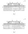
- FIGS. 3A-3Cillustrate a method of forming an embodiment of a strained transistor having the structure of the illustrative embodiment of FIG. 1 ;
- FIGS. 4A-Dillustrate a method of forming an embodiment of a strained transistor having the structure of the illustrative embodiment of FIG. 2 ;
- FIG. 5is a block diagram of an electronic device in accordance with an embodiment of the invention.
- FIG. 6is a diagram of an electronic system having devices in accordance with an embodiment of the invention.
- wafer and substrate used in the following descriptioninclude any structure having an exposed surface with which to form an integrated circuit (IC) structure or a micro electro-mechanical (MEM) structure.
- substrateis understood to include semiconductor wafers.
- substrateis also used to refer to semiconductor structures during processing, and may include other semiconductor and non-semiconductor layers that have been fabricated thereupon. Both wafer and substrate include doped and undoped semiconductors, single crystalline, polycrystalline and amorphous semiconductors, epitaxial semiconductor layers supported by a base semiconductor or insulator, as well as other semiconductor structures well known to one skilled in the art.
- conductoris understood to generally include n-type and p-type semiconductors and the term insulator or dielectric is defined to include any material that is less electrically conductive than the materials referred to as conductors or as semiconductors.
- high work functionis understood to generally include all gate electrode materials having a higher work function than that of heavily doped polycrystalline silicon.
- high dielectric constantis understood to generally include all materials having a higher dielectric constant than the 3.9 value of silicon dioxide.
- refractoryis understood to refer to any material that remains substantially unchanged during the thermal processing involved in forming transistor diffusion regions, such as the source and drain regions.
- horizontalas used in this application is defined as a plane parallel to the conventional plane or surface of a wafer or substrate, regardless of the orientation of the wafer or substrate.
- verticalrefers to a direction perpendicular to the horizontal as defined above. Prepositions, such as “on”, “side” (as in “sidewall”), “higher”, “lower”, “over” and “under” are defined with respect to the conventional plane or surface being on the top surface of the wafer or substrate, regardless of the orientation of the wafer or substrate.
- An embodimentincludes a transistor including a semiconductor substrate having a first doping type, at least two diffused regions in the substrate having an opposite doping type forming a source region and a drain region, a channel region between the source and drain regions, a dielectric layer above the channel region, a gate electrode on the dielectric layer and over the channel region, extending to include a portion of the gate electrode over part of the source and drain region.
- the transistorhas one of the portions of the gate electrode over one of the source and drain regions having an asymmetrical strain compared to the other part of the gate electrode.
- the strainmay be formed by having dissimilar materials used for sidewall spacers, or by having the spacers formed under different conditions, or by forming the gate electrode with a removed section on one side, or by adding a different material to one side of the gate electrode, or by a combination of methods.
- Typical materialsinclude polysilicon for the gate electrode, refractory metals for the different material to be added to the gate electrode, either in a trench formed in one side of the gate electrode, or attached to the top of the gate electrode, and silicon dioxide and silicon nitride for the sidewall spacers.
- Other embodimentsinclude a method of forming the transistors having an asymmetric strain, by forming a gate electrode having two dielectric spacers over a gate oxide over a substrate, removing one of the two dielectric spacers, replacing the removed dielectric spacer with a different dielectric spacer, and forming source and drain regions aligned with the two dielectric spacers.
- Another embodimentforms a photo resist mask to expose one side of the gate electrode, and to partially etch the exposed side to form a thinner layer. The etched portion may be filled by deposition of a different material.
- a MOS transistortypically has a crystalline semiconductor substrate of a first conductivity or doping type, either p type for dopant materials that provide positive charge carriers, or n type for dopant materials that provide negative charge carriers.
- a crystalline semiconductor substrate of a first conductivity or doping typeeither p type for dopant materials that provide positive charge carriers, or n type for dopant materials that provide negative charge carriers.
- the usual practiceis to refer to the source and drain diode regions as S/D regions, since the device is bidirectional.
- the substrate region between the S/D diodesis called the channel region, the distance between the S/D diodes is called the channel length, which affects the speed and drive capability of the transistor.
- the channel regionis controlled by a voltage supplied to a gate electrode disposed above, but not in direct electrical contact with, the channel region.
- the gate electrodemay be electrically separated from the channel region by an insulator layer referred to as a gate oxide.
- the gate electrodeaffects the effective doping level of the channel region by attracting the minority carrier type towards the surface of the substrate, until the minority carrier outnumbers the majority carriers at or near the surface, thus temporarily inverting the doping type of the channel region and turning the transistor to the on state.
- the amount of current the transistor can conduct when in the on state, and the rate at which the transistor can be turned off and on,depend upon numerous mutually interacting factors, including the mobility of the charge carrier, the width of the channel, the length of the channel, the doping level of the channel region, the thickness of the gate oxide, the dielectric constant of the gate oxide, the work function of the gate electrode material, and the electric field strength at the edges of the S/D regions.
- CMOScomplementary MOS
- PMOScomplementary MOS
- the PMOS devicesuse the positive charge carrier, which may be known as holes, to conduct current when in the on state, and are thus slower than NMOS devices, since holes have a lower mobility as compared to electrons.
- junction leakageOne factor affecting power consumption is what is known as junction leakage.
- One method of increasing the amount of current the transistor can conduct when in the on stateis to increase the mobility of the charge carriers by straining the crystal of the substrate in the region around the S/D junctions with the channel region.
- the strainmay cause increased power consumption by increasing the S/D junction leakage.
- strain engineering the substratemay help with increasing the drive properties of the transistors
- the strainmay hurt the device by also increasing the leakage rate of the S/D junction that is reverse biased while the device is in an operational mode. What is needed is a device that has an asymmetrical engineered strain on opposite sides of the gate electrode to provide the improvement in transistor drive obtainable with a strained substrate, while preventing the concomitant increase in junction leakage current at one of the two S/D diffusion regions.
- the asymmetrical strainmay be engineered by applying stress elements in the transistor structure in an uneven way. Any type of stress mismatch between various elements in the device structure can be used to optimize the location and type of strain desired. For example, either compressive or tensile strain layers on either the top or one of the sides of the gate electrode may result in an asymmetrical strain on the transistor.
- Specific stress configurationsmay be obtained by adjusting the deposition temperature or pressure of a chemical vapor deposition (CVD) reaction, for example silicon nitride deposition.
- CVDchemical vapor deposition
- Plasma CVD, low pressure CVD (LPCVD), sputtering, reactive sputtering, electron beam evaporation, or chemical reactionsmay also be used to form layers that have a stress mismatch.
- Mismatched layer thickness or non symmetrical geometric shapesmay also result in an applied stress to the transistor structure.
- a gate electrode having two different thicknesses over a single channel regionmay be in a stress free state at a particular operating temperature, but may form an asymmetrical strain, either compressive, tensile, or both, on the device at a different temperature due to the different amount of stress the different thicknesses of the gate electrode may be able to apply to the device.
- Several examples of methods to form asymmetrical deviceswill be provided in the illustrative embodiments provided, but other methods and structures will be apparent to one of ordinary skill in the art.
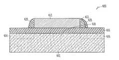
- FIG. 1illustrates an embodiment of a transistor device 100 having a structure that will apply stress to the substrate 102 in an asymmetrical way in which one of the S/D regions 104 and 106 will have an increase in the carrier mobility while the other region will not have a strain imposed that may increase the junction leakage to the channel region 108 .
- the gate dielectric or gate oxide 110has a gate electrode 112 formed of a conductive refractory material such as doped polysilicon, tungsten, titanium, titanium nitride, titanium silicide or combinations of various refractory materials.
- the gate electrode 112may also be what is known as a gate stack, formed of various layers of different materials having desired work functions and conductivities.
- This illustrative embodimenthas gate sidewall spacers 114 and 116 , which may be formed of a variety of insulating materials such as silicon dioxide, silicon nitride, silicon carbide, or other insulating materials, but the invention is not so limited, and may be applied to MOS transistors not having sidewall spacers, or to bipolar transistors.
- the sidewall spacers in the illustrative embodimentare used to prevent the S/D diffusions 104 and 106 from diffusing too far under the gate electrode 112 , and thus minimize the parasitic gate to S/D capacitance.
- the sidewall spacersare both formed of the same material, at the same time, at the same conditions, for example CVD silicon dioxide.
- the sidewall spacersmay be formed by a blanket deposition of the spacer material, which is then anisotropically etched to remove all of the material on horizontal surfaces such as the top of the gate 112 and the gate oxide 110 , but leaving the thicker material formed along the vertical walls of the sides of the gate electrode 112 to form the spacers.
- the sidewall spacersmay also have the property of protecting the gate electrode 112 from contamination during processing, and from decomposition during the thermal processing that may typically occur during the formation of the S/D regions and the remaining processing of the device of which the transistor 100 is part.
- There may be a top protective layer 118typically formed of an insulative material such as those used to form the sidewall spacers. This layer 118 may also be a remaining portion of the sidewall spacers, or a diffusion barrier.
- the gate electrode 112may have a portion 120 removed from one side of the gate electrode, for example by photo masking and etching. Even by itself, such an uneven thickness of gate electrode may create an asymmetrical strain on the substrate 102 , since the coefficient of thermal expansion (CTE) of the gate electrode, for example polysilicon, is different from that of the gate oxide 110 , for example silicon dioxide, and the operating temperature of the transistor 100 is typically different from the deposition temperature of the gate electrode, typically by hundreds of degrees C.
- CTEcoefficient of thermal expansion
- strain due to mismatched layerswas typically zero at the deposition temperature, and since the CTE values are different for the two different layers, then strain, either compressive or tensile, is imposed on the structure when the device is removed from the deposition system and cooled.
- the imposed strainis asymmetrical since the amount of stress that the thicker side of the gate electrode 112 can impose may be greater than the amount of stress from the thinner, more flexible, side of the gate electrode. More typically, the removed portion of the gate electrode 112 would be replaced with a different material having a different CTE and stress configuration.
- the conductive polysilicon 112might be partially replaced by an insulator such as silicon nitride at location 120 .
- the tungsten electrodemay have a portion removed and replaced with titanium, or other conductive material. Any two dissimilar materials may be used, or the same material formed under different conditions may be used to create a stress mismatch. This mismatch may produce the desired asymmetrical strain on the substrate 102 .
- FIG. 2illustrates a second embodiment of a device 200 having asymmetrical strain on the substrate 202 .
- the asymmetrical strainis created by the use of dissimilar materials in the gate sidewalls 214 and 216 .
- the sidewall 214may be formed of silicon nitride, while the sidewall 216 may be formed of silicon oxide.
- the different materialswill each provide a characteristic stress condition which will typically be different from each other, thus resulting in asymmetrical strain on the device 200 channel region 208 .
- the two sidewalls 214 and 216may be formed of the same material, but at different times or at different deposition conditions.
- An alternative methodmay be to create a different internal structure to one of the two sidewall structures, for example by ion implantation into one sidewall of heavy metals such as arsenic.
- the amorphous structure of one of the sidewallsmay provide a different stress condition from the partially crystallized structure of the other side.
- Another alternative structuremight be to have one of the sidewalls 214 and 216 formed of several different layers, for example sidewall 214 might be formed of a silicon dioxide layer covered by a silicon nitride layer, while sidewall 216 might be formed of a single silicon dioxide layer. Such a mismatch of different material layers on opposite sides of the gate electrode 212 creates the desired asymmetrical strain.
- FIG. 3Aillustrates an intermediate step in an illustrative method for forming the first illustrative device discussed previously.
- the illustrative transistor 300has a substrate 302 with two S/D regions 304 and 306 , which are shown in this figure for simplicity of explanation, since the S/D regions are typically formed after the gate electrode 312 is fully formed and the sidewall spacers are present.
- the gate electrode 312extends over the channel region 308 to about the edge of the S/D regions 304 and 306 .
- the gate electrode 312has a patterned photo resist layer 322 formed over a portion of the gate.
- FIG. 3Billustrates the partial removal of an exposed portion of the gate electrode 312 by means of a timed etch.
- the photo resist layer 322has been removed after completion of the etch.
- An alternative method of forming the illustrated stepmay be to deposit the gate electrode 312 as a stacked electrode with a first material having a different etch rate than a second material deposited over the first material.
- the etch processwould not have to be a timed etch, but the etch process would have to be selected to have what is known as a large etch selectivity for the second (or top) material over the first (or bottom) material to form the illustrated step.
- Another alternative formation methodwould be to use the same material for the entire gate electrode 312 , but insert a conductive etch stop material, such as titanium nitride, between the deposition of the bottom layer and the deposition of the top layer.
- a conductive etch stop materialsuch as titanium nitride
- the etch processwould have to be selected to have a large etch selectivity over the etch stop material.
- FIG. 3Cillustrates a method of filling in the step formed in the gate electrode 312 with a different material 324 .
- a materialmay be formed by means of what is known as a lift off process, or by a deposit, photo mask and etch process, or by use of an oversized mask and etch, followed by chemical mechanical polishing (CMP) processing to remove the excess material 324 over the gate electrode 312 .
- CMPchemical mechanical polishing
- the illustrated material 324is shown as having a final thickness that is greater than the height of the step cut in the gate electrode 312 , but the invention is not so limited.
- the illustrated material 324is shown as having a final width that is less than the width of the step cut in the gate electrode 312 , resulting in an area of the thin portion of gate electrode 312 that is not covered by the material 324 , but the invention is not so limited.
- the material 324may have essentially any thickness and horizontal dimension, either greater than or less than the dimension of the cutout portion of gate electrode 312 .
- the material 324may be a conductive material or an insulative material. The use of a highly conductive material may be a benefit since it would reduce the gate resistance in the case that the gate electrode 312 is formed of doped polysilicon.
- the illustrative embodimentshows two sidewall spacers 328 and 326 , but the invention is not so limited, and there may be only a single sidewall spacer, or no sidewall spacers, or the sidewall spacers 326 and 328 may be formed of different materials, or of the same material, or the same material deposited under different conditions, or the sidewalls may each be formed of various combinations of materials.
- the desired asymmetric strainmay be provided by the change in gate electrode 312 thickness from one S/D region 304 to the other S/D region 306 , or by the different material 324 attached to the gate electrode 312 , or by differences in the sidewall spacers 326 and 328 , or by a combination of these stresses.
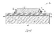
- FIG. 4Aillustrates an intermediate step in a second illustrative method for forming the second illustrative device discussed previously.
- the transistor 400has two S/D regions 404 and 406 , again shown in this figure for simplicity since the S/D regions would not yet be formed at this point in the process, separated by a channel region 408 .
- the gate insulator or oxide 410which may be formed of silicon dioxide, or of other insulating materials having a higher dielectric constant, extends at least over the channel region 408 .
- the channel regionis covered by a gate electrode 412 , which extends over the channel 408 at least to a point over the edge of S/D regions 404 and 406 .
- the gate electrode 412has sidewall spacers 420 and 422 .
- FIG. 4Bshows the process with the sidewall spacer 422 covered by patterned photo resist 424 .
- the photo resist layer 424may be used to ion implant the spacer 420 with an ion to produce damage to change the stress state of the spacer 420 .
- the photo resist layer 424in this illustrative embodiment, is used to expose the spacer 420 to an etch process selected to attack the material of the spacer 420 , for example CVD oxide, while not substantially attacking the material of the gate electrode, for example polysilicon, or of the substrate.
- FIG. 4Cshows the resulting structure after etch of the spacer 420 and the removal of the photo resist 424 .
- the transistor 400now has an asymmetric strain on the substrate 402 due to the presence of the spacer 422 on only one side of the gate electrode 412 .
- the S/D regions 404 and 406would not be present at this point in the process, and are shown for simplicity.
- the devicecould be left in this configuration, but the absence of a spacer on one side of the gate electrode would lead to a difference in the amount of overlap between the gate electrode 412 and the two S/D regions 404 and 406 , since the S/D region on the side without the spacer would diffuse much farther under the gate electrode 412 , resulting in an increase in parasitic capacitance.
- FIG. 4Dillustrates the formation of another spacer 426 , preferably formed of a different material, to replace removed spacer 420 .
- a typical material used to form spacer 426would include silicon nitride.
- spacer 426which is preferably different from the material of spacer 422 , may also cover spacer 422 with a new layer 428 .
- the mismatch of the material combinations forming the spacers on the two sides of the electrode 412will result in an asymmetric strain imposed on the device 400 .
- any difference between the materials on different portions of the channel region 408including thickness changes, material changes, spacer variations, or combinations of these factors, will result in an asymmetric strain.
- Proper positioning of the compressive or tensile stresses, and the magnitude of the imposed asymmetric strainmay be used to improve the transistor drive, while not degrading the junction leakage.
- Structures such as shown in FIG. 1 , 2 , 3 or 4may be used in any integrated circuit or transistor devices, such as flash memory devices as well as other memory, logic or information handling devices and systems.
- Embodiments of these information handling devicesinclude wireless systems, telecommunication systems, computers and integrated circuits.
- FIG. 5is a block diagram of a general electronic device in accordance with an embodiment of the invention with an electronic system 500 having one or more devices having selected portions of the circuits with devices having an asymmetric strain according to various embodiments of the present invention.
- Electronic system 500includes a controller 502 , a bus 504 , and an electronic device 506 , where bus 504 provides electrical conductivity between controller 502 and electronic device 506 .
- controller 502 and/or electronic device 506include an embodiment for a portion of the device having asymmetric strained transistors as previously discussed herein.
- Electronic system 500may include, but is not limited to, information handling devices, wireless systems, telecommunication systems, fiber optic systems, electro-optic systems, and computers.
- FIG. 6depicts a diagram of an embodiment of a system 600 having a controller 602 and a memory 606 .
- Controller 602 and/or memory 606include a portion of the circuit having asymmetric strained transistors for increase drive.
- System 600also includes an electronic apparatus 608 , and a bus 604 , where bus 604 may provide electrical conductivity and data transmission between controller 602 and electronic apparatus 608 , and between controller 602 and memory 606 .
- Bus 604may include an address, a data bus, and a control bus, each independently configured.
- Bus 604also uses common conductive lines for providing address, data, and/or control, the use of which may be regulated by controller 602 .
- electronic apparatus 608includes additional memory devices configured similarly to memory 606 .
- An embodimentincludes an additional peripheral device or devices 610 coupled to bus 604 .
- controller 602is a processor. Any of controller 602 , memory 606 , bus 604 , electronic apparatus 608 , and peripheral device or devices 610 may include transistors having an asymmetric strain in accordance with the disclosed embodiments.
- System 600may include, but is not limited to, information handling devices, telecommunication systems, and computers.
- Peripheral devices 610may include displays, additional memory, or other control devices operating with controller 602 and/or memory 606 .
Landscapes
- Engineering & Computer Science (AREA)
- Manufacturing & Machinery (AREA)
- Physics & Mathematics (AREA)
- Condensed Matter Physics & Semiconductors (AREA)
- General Physics & Mathematics (AREA)
- Computer Hardware Design (AREA)
- Microelectronics & Electronic Packaging (AREA)
- Power Engineering (AREA)
- Insulated Gate Type Field-Effect Transistor (AREA)
- Metal-Oxide And Bipolar Metal-Oxide Semiconductor Integrated Circuits (AREA)
- Chemical & Material Sciences (AREA)
- Materials Engineering (AREA)
Abstract
Description
- This application is a divisional application of U.S. application Ser. No. 11/315,031 filed on 22 Dec. 2005, which application is incorporated herein by reference in its entirety.
- This application relates generally to semiconductor devices and device fabrication and, more particularly, to the formation of CMOS gate electrodes having asymmetrical strain.
- The semiconductor device industry has a market driven need to reduce the size, cost and power consumption of integrated circuits (ICs), while increasing IC operating speed. One method of improving IC performance while reducing cost and power is to reduce the size of each of the individual transistors in the IC. As a result, virtually all electronic devices are driven to reduce or shrink the transistor size, known as scaling, including memory devices such as dynamic random access memory (DRAM), static random access memory (SRAM), and logic devices such as personal computers, laptop computers, personal digital assistants (PDAs), and other battery powered mobile devices such as cellular telephones. As the dimensions of the electronic devices are reduced, the voltage used to operate the individual logic and memory devices must be reduced for reliability reasons associated with the thinner gate dielectric thickness. An effect of reducing electronic device dimension includes increased gate dielectric leakage current and increase junction leakage. Even if the leakage currents remain the same, they become a larger percentage of the reduced overall power consumption. The thinner gate dielectrics required by the smaller IC dimensions may also have problems with increased gate leakage current levels, and the shorter channel lengths of the smaller IC devices may have increased levels of substrate leakage. Thus, there is an industry wide problem in forming scaled transistors having reduced leakage with increase drive current capabilities.
- One method used to address the need to increase the transistor drive is the use of strain engineered transistors. In particular, complementary metal oxide semiconductor (CMOS) transistors, which pair up a p type and an n type metal oxide semiconductor (MOS) transistor, to provide a very low power consumption logic gate device, have been strain engineered to increase the carrier mobility in the semiconductor material, and thus increase the drive potential of the transistors. However, the stress that is built into the transistor structure creates a strained region at both junctions of the transistor, and thus may increase even further the source/drain (S/D) leakage problem discussed above. The increase in the S/D leakage current may be a greater problem than the benefit of increased mobility and increase transistor drive.
- Thus, there exists a need to improve the carrier mobility while not increasing the S/D leakage current of the individual transistors. This need is especially felt in the low power, high performance devices such as DRAMs, low power mobile devices, and input protection devices such as electro static discharge (ESD) devices with low breakdown (BV) voltages.
- What is needed is a method to provide improved carrier mobility, with decreased S/D junction leakage, while not increasing the manufacturing complexity and cost.
FIG. 1 illustrates an embodiment of a strained transistor in accordance with an illustrative embodiment;FIG. 2 illustrates another embodiment of a strained transistor in accordance with another illustrative embodiment;FIGS. 3A-3C illustrate a method of forming an embodiment of a strained transistor having the structure of the illustrative embodiment ofFIG. 1 ;FIGS. 4A-D illustrate a method of forming an embodiment of a strained transistor having the structure of the illustrative embodiment ofFIG. 2 ;FIG. 5 is a block diagram of an electronic device in accordance with an embodiment of the invention; andFIG. 6 is a diagram of an electronic system having devices in accordance with an embodiment of the invention.- The following detailed description refers to the accompanying drawings that show, by way of illustration, specific aspects and embodiments in which the present invention may be practiced. These embodiments are described in sufficient detail to enable those skilled in the art to practice the present invention. Other embodiments may be utilized and structural, logical, and electrical changes may be made without departing from the scope of the present invention. The various embodiments are not necessarily mutually exclusive, as some embodiments can be combined with one or more other embodiments to form new embodiments.
- The terms wafer and substrate used in the following description include any structure having an exposed surface with which to form an integrated circuit (IC) structure or a micro electro-mechanical (MEM) structure. The term substrate is understood to include semiconductor wafers. The term substrate is also used to refer to semiconductor structures during processing, and may include other semiconductor and non-semiconductor layers that have been fabricated thereupon. Both wafer and substrate include doped and undoped semiconductors, single crystalline, polycrystalline and amorphous semiconductors, epitaxial semiconductor layers supported by a base semiconductor or insulator, as well as other semiconductor structures well known to one skilled in the art. The term conductor is understood to generally include n-type and p-type semiconductors and the term insulator or dielectric is defined to include any material that is less electrically conductive than the materials referred to as conductors or as semiconductors. The term high work function is understood to generally include all gate electrode materials having a higher work function than that of heavily doped polycrystalline silicon. The term high dielectric constant is understood to generally include all materials having a higher dielectric constant than the 3.9 value of silicon dioxide. The term refractory is understood to refer to any material that remains substantially unchanged during the thermal processing involved in forming transistor diffusion regions, such as the source and drain regions.
- The term “horizontal” as used in this application is defined as a plane parallel to the conventional plane or surface of a wafer or substrate, regardless of the orientation of the wafer or substrate. The term “vertical” refers to a direction perpendicular to the horizontal as defined above. Prepositions, such as “on”, “side” (as in “sidewall”), “higher”, “lower”, “over” and “under” are defined with respect to the conventional plane or surface being on the top surface of the wafer or substrate, regardless of the orientation of the wafer or substrate. The following detailed description is, therefore, not to be taken in a limiting sense, and the scope of the present invention is defined only by the appended claims, along with the full scope of equivalents to which such claims are entitled.
- An embodiment includes a transistor including a semiconductor substrate having a first doping type, at least two diffused regions in the substrate having an opposite doping type forming a source region and a drain region, a channel region between the source and drain regions, a dielectric layer above the channel region, a gate electrode on the dielectric layer and over the channel region, extending to include a portion of the gate electrode over part of the source and drain region. The transistor has one of the portions of the gate electrode over one of the source and drain regions having an asymmetrical strain compared to the other part of the gate electrode. The strain may be formed by having dissimilar materials used for sidewall spacers, or by having the spacers formed under different conditions, or by forming the gate electrode with a removed section on one side, or by adding a different material to one side of the gate electrode, or by a combination of methods. Typical materials include polysilicon for the gate electrode, refractory metals for the different material to be added to the gate electrode, either in a trench formed in one side of the gate electrode, or attached to the top of the gate electrode, and silicon dioxide and silicon nitride for the sidewall spacers.
- Other embodiments include a method of forming the transistors having an asymmetric strain, by forming a gate electrode having two dielectric spacers over a gate oxide over a substrate, removing one of the two dielectric spacers, replacing the removed dielectric spacer with a different dielectric spacer, and forming source and drain regions aligned with the two dielectric spacers. Another embodiment forms a photo resist mask to expose one side of the gate electrode, and to partially etch the exposed side to form a thinner layer. The etched portion may be filled by deposition of a different material.
- A MOS transistor typically has a crystalline semiconductor substrate of a first conductivity or doping type, either p type for dopant materials that provide positive charge carriers, or n type for dopant materials that provide negative charge carriers. There are usually at least two regions of the substrate that are doped oppositely to the substrate to form two diodes, known as the source and the drain. Either one of the two diodes may be the source or the drain, since the device is symmetrical, and the use of the terms source and drain are only significant after the transistor is biased and in operation. Thus the usual practice is to refer to the source and drain diode regions as S/D regions, since the device is bidirectional. The substrate region between the S/D diodes is called the channel region, the distance between the S/D diodes is called the channel length, which affects the speed and drive capability of the transistor. The length of the S/D regions in the direction perpendicular to the channel length, but in the plane of the substrate, is called the transistor width, which also affects the drive capability of the transistor.
- The channel region is controlled by a voltage supplied to a gate electrode disposed above, but not in direct electrical contact with, the channel region. The gate electrode may be electrically separated from the channel region by an insulator layer referred to as a gate oxide. The gate electrode affects the effective doping level of the channel region by attracting the minority carrier type towards the surface of the substrate, until the minority carrier outnumbers the majority carriers at or near the surface, thus temporarily inverting the doping type of the channel region and turning the transistor to the on state.
- The amount of current the transistor can conduct when in the on state, and the rate at which the transistor can be turned off and on, depend upon numerous mutually interacting factors, including the mobility of the charge carrier, the width of the channel, the length of the channel, the doping level of the channel region, the thickness of the gate oxide, the dielectric constant of the gate oxide, the work function of the gate electrode material, and the electric field strength at the edges of the S/D regions.
- Another transistor property of interest, particularly in low power applications such as mobile phones, mobile computers and personal digital assistants (PDAs), is power consumption. One method of reducing the operating power consumption of a particular device is to use what is known as complementary MOS (CMOS) devices that pair a NMOS transistor with a PMOS transistor so that the only time that the logic gate conducts large amounts of power is during the short interval when the logic state is changing from low to high, or vice versa. However, the PMOS devices use the positive charge carrier, which may be known as holes, to conduct current when in the on state, and are thus slower than NMOS devices, since holes have a lower mobility as compared to electrons. One factor affecting power consumption is what is known as junction leakage.
- One method of increasing the amount of current the transistor can conduct when in the on state, also known as the transistor drive, is to increase the mobility of the charge carriers by straining the crystal of the substrate in the region around the S/D junctions with the channel region. However, the strain may cause increased power consumption by increasing the S/D junction leakage. Thus, while strain engineering the substrate may help with increasing the drive properties of the transistors, the strain may hurt the device by also increasing the leakage rate of the S/D junction that is reverse biased while the device is in an operational mode. What is needed is a device that has an asymmetrical engineered strain on opposite sides of the gate electrode to provide the improvement in transistor drive obtainable with a strained substrate, while preventing the concomitant increase in junction leakage current at one of the two S/D diffusion regions.
- The asymmetrical strain may be engineered by applying stress elements in the transistor structure in an uneven way. Any type of stress mismatch between various elements in the device structure can be used to optimize the location and type of strain desired. For example, either compressive or tensile strain layers on either the top or one of the sides of the gate electrode may result in an asymmetrical strain on the transistor. Specific stress configurations may be obtained by adjusting the deposition temperature or pressure of a chemical vapor deposition (CVD) reaction, for example silicon nitride deposition. Plasma CVD, low pressure CVD (LPCVD), sputtering, reactive sputtering, electron beam evaporation, or chemical reactions may also be used to form layers that have a stress mismatch. Mismatched layer thickness or non symmetrical geometric shapes may also result in an applied stress to the transistor structure. For example, a gate electrode having two different thicknesses over a single channel region may be in a stress free state at a particular operating temperature, but may form an asymmetrical strain, either compressive, tensile, or both, on the device at a different temperature due to the different amount of stress the different thicknesses of the gate electrode may be able to apply to the device. Several examples of methods to form asymmetrical devices will be provided in the illustrative embodiments provided, but other methods and structures will be apparent to one of ordinary skill in the art.
FIG. 1 illustrates an embodiment of atransistor device 100 having a structure that will apply stress to thesubstrate 102 in an asymmetrical way in which one of the S/D regions channel region 108. In this illustrative embodiment, the gate dielectric orgate oxide 110 has agate electrode 112 formed of a conductive refractory material such as doped polysilicon, tungsten, titanium, titanium nitride, titanium silicide or combinations of various refractory materials. Thegate electrode 112 may also be what is known as a gate stack, formed of various layers of different materials having desired work functions and conductivities.- This illustrative embodiment has
gate sidewall spacers gate electrode 112, and thus minimize the parasitic gate to S/D capacitance. In this illustrative embodiment the sidewall spacers are both formed of the same material, at the same time, at the same conditions, for example CVD silicon dioxide. As a result of both spacers being formed of the same material under the same conditions, the strain applied to thesubstrate 102 is symmetrical. The sidewall spacers may be formed by a blanket deposition of the spacer material, which is then anisotropically etched to remove all of the material on horizontal surfaces such as the top of thegate 112 and thegate oxide 110, but leaving the thicker material formed along the vertical walls of the sides of thegate electrode 112 to form the spacers. - The sidewall spacers may also have the property of protecting the
gate electrode 112 from contamination during processing, and from decomposition during the thermal processing that may typically occur during the formation of the S/D regions and the remaining processing of the device of which thetransistor 100 is part. There may be a topprotective layer 118, typically formed of an insulative material such as those used to form the sidewall spacers. Thislayer 118 may also be a remaining portion of the sidewall spacers, or a diffusion barrier. - The
gate electrode 112, as illustrated in this embodiment, may have aportion 120 removed from one side of the gate electrode, for example by photo masking and etching. Even by itself, such an uneven thickness of gate electrode may create an asymmetrical strain on thesubstrate 102, since the coefficient of thermal expansion (CTE) of the gate electrode, for example polysilicon, is different from that of thegate oxide 110, for example silicon dioxide, and the operating temperature of thetransistor 100 is typically different from the deposition temperature of the gate electrode, typically by hundreds of degrees C. Since the strain due to mismatched layers was typically zero at the deposition temperature, and since the CTE values are different for the two different layers, then strain, either compressive or tensile, is imposed on the structure when the device is removed from the deposition system and cooled. The imposed strain is asymmetrical since the amount of stress that the thicker side of thegate electrode 112 can impose may be greater than the amount of stress from the thinner, more flexible, side of the gate electrode. More typically, the removed portion of thegate electrode 112 would be replaced with a different material having a different CTE and stress configuration. As an example, theconductive polysilicon 112 might be partially replaced by an insulator such as silicon nitride atlocation 120. In another embodiment, the tungsten electrode may have a portion removed and replaced with titanium, or other conductive material. Any two dissimilar materials may be used, or the same material formed under different conditions may be used to create a stress mismatch. This mismatch may produce the desired asymmetrical strain on thesubstrate 102. FIG. 2 illustrates a second embodiment of adevice 200 having asymmetrical strain on thesubstrate 202. In this embodiment the asymmetrical strain is created by the use of dissimilar materials in the gate sidewalls214 and216. For example, thesidewall 214 may be formed of silicon nitride, while thesidewall 216 may be formed of silicon oxide. The different materials will each provide a characteristic stress condition which will typically be different from each other, thus resulting in asymmetrical strain on thedevice 200channel region 208. In the alternative, the twosidewalls - An alternative method may be to create a different internal structure to one of the two sidewall structures, for example by ion implantation into one sidewall of heavy metals such as arsenic. The amorphous structure of one of the sidewalls may provide a different stress condition from the partially crystallized structure of the other side. Another alternative structure might be to have one of the
sidewalls example sidewall 214 might be formed of a silicon dioxide layer covered by a silicon nitride layer, whilesidewall 216 might be formed of a single silicon dioxide layer. Such a mismatch of different material layers on opposite sides of thegate electrode 212 creates the desired asymmetrical strain. FIG. 3A illustrates an intermediate step in an illustrative method for forming the first illustrative device discussed previously. Theillustrative transistor 300 has asubstrate 302 with two S/D regions gate electrode 312 is fully formed and the sidewall spacers are present. Thegate electrode 312 extends over thechannel region 308 to about the edge of the S/D regions gate electrode 312 has a patterned photo resistlayer 322 formed over a portion of the gate.FIG. 3B illustrates the partial removal of an exposed portion of thegate electrode 312 by means of a timed etch. The photo resistlayer 322 has been removed after completion of the etch. An alternative method of forming the illustrated step may be to deposit thegate electrode 312 as a stacked electrode with a first material having a different etch rate than a second material deposited over the first material. In this illustrative embodiment, the etch process would not have to be a timed etch, but the etch process would have to be selected to have what is known as a large etch selectivity for the second (or top) material over the first (or bottom) material to form the illustrated step.- Another alternative formation method would be to use the same material for the
entire gate electrode 312, but insert a conductive etch stop material, such as titanium nitride, between the deposition of the bottom layer and the deposition of the top layer. In this illustrative method, the etch process would have to be selected to have a large etch selectivity over the etch stop material. FIG. 3C illustrates a method of filling in the step formed in thegate electrode 312 with adifferent material 324. Such a material may be formed by means of what is known as a lift off process, or by a deposit, photo mask and etch process, or by use of an oversized mask and etch, followed by chemical mechanical polishing (CMP) processing to remove theexcess material 324 over thegate electrode 312. The illustratedmaterial 324 is shown as having a final thickness that is greater than the height of the step cut in thegate electrode 312, but the invention is not so limited. The illustratedmaterial 324 is shown as having a final width that is less than the width of the step cut in thegate electrode 312, resulting in an area of the thin portion ofgate electrode 312 that is not covered by thematerial 324, but the invention is not so limited. Thematerial 324 may have essentially any thickness and horizontal dimension, either greater than or less than the dimension of the cutout portion ofgate electrode 312. Thematerial 324 may be a conductive material or an insulative material. The use of a highly conductive material may be a benefit since it would reduce the gate resistance in the case that thegate electrode 312 is formed of doped polysilicon.- The illustrative embodiment shows two
sidewall spacers sidewall spacers gate electrode 312 thickness from one S/D region 304 to the other S/D region 306, or by thedifferent material 324 attached to thegate electrode 312, or by differences in thesidewall spacers FIG. 4A illustrates an intermediate step in a second illustrative method for forming the second illustrative device discussed previously. Thetransistor 400 has two S/D regions channel region 408. The gate insulator oroxide 410, which may be formed of silicon dioxide, or of other insulating materials having a higher dielectric constant, extends at least over thechannel region 408. The channel region is covered by agate electrode 412, which extends over thechannel 408 at least to a point over the edge of S/D regions gate electrode 412 hassidewall spacers FIG. 4B shows the process with thesidewall spacer 422 covered by patterned photo resist424. The photo resistlayer 424 may be used to ion implant thespacer 420 with an ion to produce damage to change the stress state of thespacer 420. The photo resistlayer 424, in this illustrative embodiment, is used to expose thespacer 420 to an etch process selected to attack the material of thespacer 420, for example CVD oxide, while not substantially attacking the material of the gate electrode, for example polysilicon, or of the substrate.FIG. 4C shows the resulting structure after etch of thespacer 420 and the removal of the photo resist424. Thetransistor 400 now has an asymmetric strain on thesubstrate 402 due to the presence of thespacer 422 on only one side of thegate electrode 412. Again note that the S/D regions gate electrode 412 and the two S/D regions gate electrode 412, resulting in an increase in parasitic capacitance.FIG. 4D illustrates the formation of another spacer426, preferably formed of a different material, to replace removedspacer 420. A typical material used to form spacer426 would include silicon nitride.- The material of spacer426, which is preferably different from the material of
spacer 422, may also cover spacer422 with anew layer 428. The mismatch of the material combinations forming the spacers on the two sides of theelectrode 412 will result in an asymmetric strain imposed on thedevice 400. - Any difference between the materials on different portions of the
channel region 408, including thickness changes, material changes, spacer variations, or combinations of these factors, will result in an asymmetric strain. Proper positioning of the compressive or tensile stresses, and the magnitude of the imposed asymmetric strain may be used to improve the transistor drive, while not degrading the junction leakage. - Structures such as shown in
FIG. 1 ,2,3 or4 may be used in any integrated circuit or transistor devices, such as flash memory devices as well as other memory, logic or information handling devices and systems. Embodiments of these information handling devices include wireless systems, telecommunication systems, computers and integrated circuits. FIG. 5 is a block diagram of a general electronic device in accordance with an embodiment of the invention with anelectronic system 500 having one or more devices having selected portions of the circuits with devices having an asymmetric strain according to various embodiments of the present invention.Electronic system 500 includes acontroller 502, abus 504, and anelectronic device 506, wherebus 504 provides electrical conductivity betweencontroller 502 andelectronic device 506. In various embodiments,controller 502 and/orelectronic device 506 include an embodiment for a portion of the device having asymmetric strained transistors as previously discussed herein.Electronic system 500 may include, but is not limited to, information handling devices, wireless systems, telecommunication systems, fiber optic systems, electro-optic systems, and computers.FIG. 6 depicts a diagram of an embodiment of asystem 600 having acontroller 602 and amemory 606.Controller 602 and/ormemory 606 include a portion of the circuit having asymmetric strained transistors for increase drive.System 600 also includes anelectronic apparatus 608, and abus 604, wherebus 604 may provide electrical conductivity and data transmission betweencontroller 602 andelectronic apparatus 608, and betweencontroller 602 andmemory 606.Bus 604 may include an address, a data bus, and a control bus, each independently configured.Bus 604 also uses common conductive lines for providing address, data, and/or control, the use of which may be regulated bycontroller 602. In an embodiment,electronic apparatus 608 includes additional memory devices configured similarly tomemory 606. An embodiment includes an additional peripheral device ordevices 610 coupled tobus 604. In anembodiment controller 602 is a processor. Any ofcontroller 602,memory 606,bus 604,electronic apparatus 608, and peripheral device ordevices 610 may include transistors having an asymmetric strain in accordance with the disclosed embodiments.System 600 may include, but is not limited to, information handling devices, telecommunication systems, and computers.Peripheral devices 610 may include displays, additional memory, or other control devices operating withcontroller 602 and/ormemory 606.- Although specific embodiments have been illustrated and described herein, it will be appreciated by those of ordinary skill in the art that any arrangement that is calculated to achieve the same purpose may be substituted for the specific embodiments shown. This application is intended to cover any adaptations or variations of embodiments of the present invention. It is to be understood that the above description is intended to be illustrative, and not restrictive, and that the phraseology or terminology employed herein is for the purpose of description and not of limitation. Combinations of the above embodiments and other embodiments will be apparent to those of skill in the art upon studying the above description. The scope of the present invention includes any other applications in which embodiments of the above structures and fabrication methods are used. The scope of the embodiments of the present invention should be determined with reference to the appended claims, along with the full scope of equivalents to which such claims are entitled.
Claims (31)
Priority Applications (4)
| Application Number | Priority Date | Filing Date | Title |
|---|---|---|---|
| US12/697,991US8093658B2 (en) | 2005-12-22 | 2010-02-01 | Electronic device with asymmetric gate strain |
| US13/345,446US8803240B2 (en) | 2005-12-22 | 2012-01-06 | Electronic device with asymmetric gate strain |
| US14/456,435US9356145B2 (en) | 2005-12-22 | 2014-08-11 | Electronic device with asymmetric gate strain |
| US15/165,951US9780184B2 (en) | 2005-12-22 | 2016-05-26 | Electronic device with asymmetric gate strain |
Applications Claiming Priority (2)
| Application Number | Priority Date | Filing Date | Title |
|---|---|---|---|
| US11/315,031US7656049B2 (en) | 2005-12-22 | 2005-12-22 | CMOS device with asymmetric gate strain |
| US12/697,991US8093658B2 (en) | 2005-12-22 | 2010-02-01 | Electronic device with asymmetric gate strain |
Related Parent Applications (1)
| Application Number | Title | Priority Date | Filing Date |
|---|---|---|---|
| US11/315,031DivisionUS7656049B2 (en) | 2005-12-22 | 2005-12-22 | CMOS device with asymmetric gate strain |
Related Child Applications (1)
| Application Number | Title | Priority Date | Filing Date |
|---|---|---|---|
| US13/345,446DivisionUS8803240B2 (en) | 2005-12-22 | 2012-01-06 | Electronic device with asymmetric gate strain |
Publications (2)
| Publication Number | Publication Date |
|---|---|
| US20100133612A1true US20100133612A1 (en) | 2010-06-03 |
| US8093658B2 US8093658B2 (en) | 2012-01-10 |
Family
ID=38057283
Family Applications (5)
| Application Number | Title | Priority Date | Filing Date |
|---|---|---|---|
| US11/315,031Expired - Fee RelatedUS7656049B2 (en) | 2005-12-22 | 2005-12-22 | CMOS device with asymmetric gate strain |
| US12/697,991ActiveUS8093658B2 (en) | 2005-12-22 | 2010-02-01 | Electronic device with asymmetric gate strain |
| US13/345,446Active2026-01-28US8803240B2 (en) | 2005-12-22 | 2012-01-06 | Electronic device with asymmetric gate strain |
| US14/456,435ActiveUS9356145B2 (en) | 2005-12-22 | 2014-08-11 | Electronic device with asymmetric gate strain |
| US15/165,951ActiveUS9780184B2 (en) | 2005-12-22 | 2016-05-26 | Electronic device with asymmetric gate strain |
Family Applications Before (1)
| Application Number | Title | Priority Date | Filing Date |
|---|---|---|---|
| US11/315,031Expired - Fee RelatedUS7656049B2 (en) | 2005-12-22 | 2005-12-22 | CMOS device with asymmetric gate strain |
Family Applications After (3)
| Application Number | Title | Priority Date | Filing Date |
|---|---|---|---|
| US13/345,446Active2026-01-28US8803240B2 (en) | 2005-12-22 | 2012-01-06 | Electronic device with asymmetric gate strain |
| US14/456,435ActiveUS9356145B2 (en) | 2005-12-22 | 2014-08-11 | Electronic device with asymmetric gate strain |
| US15/165,951ActiveUS9780184B2 (en) | 2005-12-22 | 2016-05-26 | Electronic device with asymmetric gate strain |
Country Status (2)
| Country | Link |
|---|---|
| US (5) | US7656049B2 (en) |
| WO (1) | WO2007075755A2 (en) |
Cited By (3)
| Publication number | Priority date | Publication date | Assignee | Title |
|---|---|---|---|---|
| US8377754B1 (en) | 2011-10-10 | 2013-02-19 | International Business Machines Corporation | Stress enhanced junction engineering for latchup SCR |
| US8803240B2 (en) | 2005-12-22 | 2014-08-12 | Micron Technology, Inc. | Electronic device with asymmetric gate strain |
| CN107968053A (en)* | 2016-10-20 | 2018-04-27 | 中芯国际集成电路制造(上海)有限公司 | Semiconductor devices and forming method thereof |
Families Citing this family (17)
| Publication number | Priority date | Publication date | Assignee | Title |
|---|---|---|---|---|
| JP2007180537A (en)* | 2005-12-28 | 2007-07-12 | Dongbu Electronics Co Ltd | CMOS image sensor and manufacturing method thereof |
| US7494886B2 (en)* | 2007-01-12 | 2009-02-24 | International Business Machines Corporation | Uniaxial strain relaxation of biaxial-strained thin films using ion implantation |
| US20090309139A1 (en)* | 2008-06-13 | 2009-12-17 | International Business Machines Corporation | Asymmetric gate electrode and method of manufacture |
| KR20100081765A (en)* | 2009-01-07 | 2010-07-15 | 삼성전자주식회사 | Fabricating method of semiconductor integrated circuit devices |
| US8461034B2 (en) | 2010-10-20 | 2013-06-11 | International Business Machines Corporation | Localized implant into active region for enhanced stress |
| CN103515435B (en)* | 2012-06-26 | 2016-12-21 | 中芯国际集成电路制造(上海)有限公司 | MOS transistor and forming method thereof, SRAM memory cell circuit |
| US20140291761A1 (en) | 2013-03-29 | 2014-10-02 | International Business Machines Corporation | Asymmetric Spacers |
| US9064901B1 (en)* | 2013-12-23 | 2015-06-23 | International Business Machines Corporation | Fin density control of multigate devices through sidewall image transfer processes |
| US9240482B2 (en) | 2014-05-30 | 2016-01-19 | Globalfoundries Inc. | Asymmetric stressor DRAM |
| US9190488B1 (en)* | 2014-08-13 | 2015-11-17 | Globalfoundries Inc. | Methods of forming gate structure of semiconductor devices and the resulting devices |
| KR102248667B1 (en)* | 2014-08-19 | 2021-05-07 | 인텔 코포레이션 | Transistor gate metal with laterally graduated work function |
| CN106298923B (en)* | 2015-06-02 | 2020-10-09 | 联华电子股份有限公司 | High-voltage metal-oxide-semiconductor transistor device and method for manufacturing the same |
| US10734511B2 (en) | 2016-03-31 | 2020-08-04 | Intel Corporation | High mobility asymmetric field effect transistors with a band-offset semiconductor drain spacer |
| US10079290B2 (en)* | 2016-12-30 | 2018-09-18 | United Microelectronics Corp. | Semiconductor device having asymmetric spacer structures |
| WO2018182627A1 (en)* | 2017-03-30 | 2018-10-04 | Intel Corporation | Transistors including asymmetric gate spacers |
| CN110943129A (en)* | 2018-09-25 | 2020-03-31 | 长鑫存储技术有限公司 | Semiconductor device and method for manufacturing the same |
| CN120111934B (en)* | 2025-05-08 | 2025-09-09 | 合肥晶合集成电路股份有限公司 | Semiconductor structure and preparation method thereof |
Citations (33)
| Publication number | Priority date | Publication date | Assignee | Title |
|---|---|---|---|---|
| US5741737A (en)* | 1996-06-27 | 1998-04-21 | Cypress Semiconductor Corporation | MOS transistor with ramped gate oxide thickness and method for making same |
| US6503833B1 (en)* | 2000-11-15 | 2003-01-07 | International Business Machines Corporation | Self-aligned silicide (salicide) process for strained silicon MOSFET ON SiGe and structure formed thereby |
| US20030049893A1 (en)* | 2001-06-08 | 2003-03-13 | Matthew Currie | Method for isolating semiconductor devices |
| US20030052333A1 (en)* | 1999-12-28 | 2003-03-20 | Intel Corporation | Field effect transistor structure with self-aligned raised source/drain extensions |
| US6583000B1 (en)* | 2002-02-07 | 2003-06-24 | Sharp Laboratories Of America, Inc. | Process integration of Si1-xGex CMOS with Si1-xGex relaxation after STI formation |
| US20030116781A1 (en)* | 2001-12-26 | 2003-06-26 | Kabushiki Kaisha Toshiba | Semiconductor device and method of manufacturing the same |
| US6593191B2 (en)* | 2000-05-26 | 2003-07-15 | Amberwave Systems Corporation | Buried channel strained silicon FET using a supply layer created through ion implantation |
| US20040113217A1 (en)* | 2002-12-12 | 2004-06-17 | International Business Machines Corporation | Stress inducing spacers |
| US6774015B1 (en)* | 2002-12-19 | 2004-08-10 | International Business Machines Corporation | Strained silicon-on-insulator (SSOI) and method to form the same |
| US6787423B1 (en)* | 2002-12-09 | 2004-09-07 | Advanced Micro Devices, Inc. | Strained-silicon semiconductor device |
| US20040178406A1 (en)* | 2003-03-15 | 2004-09-16 | Chu Jack Oon | Dual strain-state SiGe layers for microelectronics |
| US20040232422A1 (en)* | 2003-05-21 | 2004-11-25 | Micron Technology, Inc. | Wafer gettering using relaxed silicon germanium epitaxial proximity layers |
| US6825086B2 (en)* | 2003-01-17 | 2004-11-30 | Sharp Laboratories Of America, Inc. | Strained-silicon channel CMOS with sacrificial shallow trench isolation oxide liner |
| US20050035404A1 (en)* | 2003-08-11 | 2005-02-17 | Samsung Electronics Co., Ltd. | High voltage transistor and method of manufacturing the same |
| US6893936B1 (en)* | 2004-06-29 | 2005-05-17 | International Business Machines Corporation | Method of Forming strained SI/SIGE on insulator with silicon germanium buffer |
| US6903384B2 (en)* | 2003-01-15 | 2005-06-07 | Sharp Laboratories Of America, Inc. | System and method for isolating silicon germanium dislocation regions in strained-silicon CMOS applications |
| US20050142768A1 (en)* | 2003-12-31 | 2005-06-30 | Nick Lindert | Controlled faceting of source/drain regions |
| US20050145919A1 (en)* | 2004-01-02 | 2005-07-07 | Ko-Hsing Chang | [multi-level memory cell] |
| US6955952B2 (en)* | 2003-03-07 | 2005-10-18 | Taiwan Semiconductor Manufacturing Company, Ltd. | Strain balanced structure with a tensile strained silicon channel and a compressive strained silicon-germanium channel for CMOS performance enhancement |
| US20050285097A1 (en)* | 2004-06-24 | 2005-12-29 | Huiling Shang | Integration of strained Ge into advanced CMOS technology |
| US6982208B2 (en)* | 2004-05-03 | 2006-01-03 | Taiwan Semiconductor Manufacturing Co., Ltd. | Method for producing high throughput strained-Si channel MOSFETS |
| US6987037B2 (en)* | 2003-05-07 | 2006-01-17 | Micron Technology, Inc. | Strained Si/SiGe structures by ion implantation |
| US7033893B1 (en)* | 2002-12-12 | 2006-04-25 | Advanced Micro Devices, Inc. | CMOS devices with balanced drive currents based on SiGe |
| US7060632B2 (en)* | 2002-03-14 | 2006-06-13 | Amberwave Systems Corporation | Methods for fabricating strained layers on semiconductor substrates |
| US7078742B2 (en)* | 2003-07-25 | 2006-07-18 | Taiwan Semiconductor Manufacturing Co., Ltd. | Strained-channel semiconductor structure and method of fabricating the same |
| US7084460B2 (en)* | 2003-11-03 | 2006-08-01 | International Business Machines Corporation | Method for fabricating SiGe-on-insulator (SGOI) and Ge-on-insulator (GOI) substrates |
| US20060170016A1 (en)* | 2005-02-01 | 2006-08-03 | Freescale Semiconductor Inc. | Asymmetric spacers and asymmetric source/drain extension layers |
| US20060172502A1 (en)* | 2005-01-28 | 2006-08-03 | Texas Instruments Incorporated | Methods, systems and structures for forming semiconductor structures incorporating high-temperature processing steps |
| US7091522B2 (en)* | 2003-07-29 | 2006-08-15 | Industrial Research Technology Institute | Strained silicon carbon alloy MOSFET structure and fabrication method thereof |
| US20060199310A1 (en)* | 2005-03-04 | 2006-09-07 | Yukio Nakabayashi | Semiconductor integrated circuit and semiconductor device |
| US7112495B2 (en)* | 2003-08-15 | 2006-09-26 | Taiwan Semiconductor Manufacturing Company, Ltd. | Structure and method of a strained channel transistor and a second semiconductor component in an integrated circuit |
| US7132349B2 (en)* | 2002-11-26 | 2006-11-07 | Samsung Electronics Co. Ltd. | Methods of forming integrated circuits structures including epitaxial silicon layers in active regions |
| US20070145430A1 (en)* | 2005-12-22 | 2007-06-28 | Micron Technology, Inc. | CMOS device with asymmetric gate strain |
Family Cites Families (7)
| Publication number | Priority date | Publication date | Assignee | Title |
|---|---|---|---|---|
| FR2718287B1 (en) | 1994-03-31 | 1996-08-02 | Alain Straboni | Method for manufacturing an insulated gate field effect transistor, in particular of reduced channel length, and corresponding transistor. |
| DE19626089C2 (en) | 1996-06-28 | 2002-01-31 | Siemens Ag | Memory cell and method for its manufacture |
| KR100223927B1 (en) | 1996-07-31 | 1999-10-15 | 구본준 | Field effect transistor and manufacture thereof |
| US6229184B1 (en)* | 1999-02-16 | 2001-05-08 | Advanced Micro Devices, Inc. | Semiconductor device with a modulated gate oxide thickness |
| US6909151B2 (en)* | 2003-06-27 | 2005-06-21 | Intel Corporation | Nonplanar device with stress incorporation layer and method of fabrication |
| KR100526476B1 (en) | 2003-12-31 | 2005-11-08 | 동부아남반도체 주식회사 | Method for fabricating split gate flash memory device |
| DE102004063199B4 (en) | 2004-12-23 | 2010-11-25 | Atmel Automotive Gmbh | Pulse generator and method for generating a pulse train |
- 2005
- 2005-12-22USUS11/315,031patent/US7656049B2/ennot_activeExpired - Fee Related
- 2006
- 2006-12-18WOPCT/US2006/048547patent/WO2007075755A2/enactiveApplication Filing
- 2010
- 2010-02-01USUS12/697,991patent/US8093658B2/enactiveActive
- 2012
- 2012-01-06USUS13/345,446patent/US8803240B2/enactiveActive
- 2014
- 2014-08-11USUS14/456,435patent/US9356145B2/enactiveActive
- 2016
- 2016-05-26USUS15/165,951patent/US9780184B2/enactiveActive
Patent Citations (38)
| Publication number | Priority date | Publication date | Assignee | Title |
|---|---|---|---|---|
| US5741737A (en)* | 1996-06-27 | 1998-04-21 | Cypress Semiconductor Corporation | MOS transistor with ramped gate oxide thickness and method for making same |
| US20020145166A1 (en)* | 1996-06-27 | 2002-10-10 | Cypress Semiconductor Corporation | MOS transistor with ramped gate oxide thickness and method for making same |
| US20030052333A1 (en)* | 1999-12-28 | 2003-03-20 | Intel Corporation | Field effect transistor structure with self-aligned raised source/drain extensions |
| US6593191B2 (en)* | 2000-05-26 | 2003-07-15 | Amberwave Systems Corporation | Buried channel strained silicon FET using a supply layer created through ion implantation |
| US6503833B1 (en)* | 2000-11-15 | 2003-01-07 | International Business Machines Corporation | Self-aligned silicide (salicide) process for strained silicon MOSFET ON SiGe and structure formed thereby |
| US20030049893A1 (en)* | 2001-06-08 | 2003-03-13 | Matthew Currie | Method for isolating semiconductor devices |
| US20030116781A1 (en)* | 2001-12-26 | 2003-06-26 | Kabushiki Kaisha Toshiba | Semiconductor device and method of manufacturing the same |
| US6583000B1 (en)* | 2002-02-07 | 2003-06-24 | Sharp Laboratories Of America, Inc. | Process integration of Si1-xGex CMOS with Si1-xGex relaxation after STI formation |
| US7060632B2 (en)* | 2002-03-14 | 2006-06-13 | Amberwave Systems Corporation | Methods for fabricating strained layers on semiconductor substrates |
| US7132349B2 (en)* | 2002-11-26 | 2006-11-07 | Samsung Electronics Co. Ltd. | Methods of forming integrated circuits structures including epitaxial silicon layers in active regions |
| US6787423B1 (en)* | 2002-12-09 | 2004-09-07 | Advanced Micro Devices, Inc. | Strained-silicon semiconductor device |
| US7033893B1 (en)* | 2002-12-12 | 2006-04-25 | Advanced Micro Devices, Inc. | CMOS devices with balanced drive currents based on SiGe |
| US20040113217A1 (en)* | 2002-12-12 | 2004-06-17 | International Business Machines Corporation | Stress inducing spacers |
| US6774015B1 (en)* | 2002-12-19 | 2004-08-10 | International Business Machines Corporation | Strained silicon-on-insulator (SSOI) and method to form the same |
| US6903384B2 (en)* | 2003-01-15 | 2005-06-07 | Sharp Laboratories Of America, Inc. | System and method for isolating silicon germanium dislocation regions in strained-silicon CMOS applications |
| US6825086B2 (en)* | 2003-01-17 | 2004-11-30 | Sharp Laboratories Of America, Inc. | Strained-silicon channel CMOS with sacrificial shallow trench isolation oxide liner |
| US6955952B2 (en)* | 2003-03-07 | 2005-10-18 | Taiwan Semiconductor Manufacturing Company, Ltd. | Strain balanced structure with a tensile strained silicon channel and a compressive strained silicon-germanium channel for CMOS performance enhancement |
| US20050156268A1 (en)* | 2003-03-15 | 2005-07-21 | International Business Machines Corporation | Dual strain-state SiGe layers for microelectronics |
| US6963078B2 (en)* | 2003-03-15 | 2005-11-08 | International Business Machines Corporation | Dual strain-state SiGe layers for microelectronics |
| US20040178406A1 (en)* | 2003-03-15 | 2004-09-16 | Chu Jack Oon | Dual strain-state SiGe layers for microelectronics |
| US6987037B2 (en)* | 2003-05-07 | 2006-01-17 | Micron Technology, Inc. | Strained Si/SiGe structures by ion implantation |
| US20060258123A1 (en)* | 2003-05-21 | 2006-11-16 | Micron Technology, Inc. | Wafer gettering using relaxed silicon germanium epitaxial proximity layers |
| US20040232422A1 (en)* | 2003-05-21 | 2004-11-25 | Micron Technology, Inc. | Wafer gettering using relaxed silicon germanium epitaxial proximity layers |
| US7078742B2 (en)* | 2003-07-25 | 2006-07-18 | Taiwan Semiconductor Manufacturing Co., Ltd. | Strained-channel semiconductor structure and method of fabricating the same |
| US7091522B2 (en)* | 2003-07-29 | 2006-08-15 | Industrial Research Technology Institute | Strained silicon carbon alloy MOSFET structure and fabrication method thereof |
| US20050035404A1 (en)* | 2003-08-11 | 2005-02-17 | Samsung Electronics Co., Ltd. | High voltage transistor and method of manufacturing the same |
| US7112495B2 (en)* | 2003-08-15 | 2006-09-26 | Taiwan Semiconductor Manufacturing Company, Ltd. | Structure and method of a strained channel transistor and a second semiconductor component in an integrated circuit |
| US7084460B2 (en)* | 2003-11-03 | 2006-08-01 | International Business Machines Corporation | Method for fabricating SiGe-on-insulator (SGOI) and Ge-on-insulator (GOI) substrates |
| US20050142768A1 (en)* | 2003-12-31 | 2005-06-30 | Nick Lindert | Controlled faceting of source/drain regions |
| US20050145919A1 (en)* | 2004-01-02 | 2005-07-07 | Ko-Hsing Chang | [multi-level memory cell] |
| US6982208B2 (en)* | 2004-05-03 | 2006-01-03 | Taiwan Semiconductor Manufacturing Co., Ltd. | Method for producing high throughput strained-Si channel MOSFETS |
| US20050285097A1 (en)* | 2004-06-24 | 2005-12-29 | Huiling Shang | Integration of strained Ge into advanced CMOS technology |
| US6893936B1 (en)* | 2004-06-29 | 2005-05-17 | International Business Machines Corporation | Method of Forming strained SI/SIGE on insulator with silicon germanium buffer |
| US20060172502A1 (en)* | 2005-01-28 | 2006-08-03 | Texas Instruments Incorporated | Methods, systems and structures for forming semiconductor structures incorporating high-temperature processing steps |
| US20060170016A1 (en)* | 2005-02-01 | 2006-08-03 | Freescale Semiconductor Inc. | Asymmetric spacers and asymmetric source/drain extension layers |
| US20060199310A1 (en)* | 2005-03-04 | 2006-09-07 | Yukio Nakabayashi | Semiconductor integrated circuit and semiconductor device |
| US20070145430A1 (en)* | 2005-12-22 | 2007-06-28 | Micron Technology, Inc. | CMOS device with asymmetric gate strain |
| US7656049B2 (en)* | 2005-12-22 | 2010-02-02 | Micron Technology, Inc. | CMOS device with asymmetric gate strain |
Cited By (6)
| Publication number | Priority date | Publication date | Assignee | Title |
|---|---|---|---|---|
| US8803240B2 (en) | 2005-12-22 | 2014-08-12 | Micron Technology, Inc. | Electronic device with asymmetric gate strain |
| US9356145B2 (en) | 2005-12-22 | 2016-05-31 | Micron Technology, Inc. | Electronic device with asymmetric gate strain |
| US9780184B2 (en) | 2005-12-22 | 2017-10-03 | Micron Technology, Inc. | Electronic device with asymmetric gate strain |
| US8377754B1 (en) | 2011-10-10 | 2013-02-19 | International Business Machines Corporation | Stress enhanced junction engineering for latchup SCR |
| US8674400B2 (en) | 2011-10-10 | 2014-03-18 | International Business Machines Corporation | Stress enhanced junction engineering for latchup SCR |
| CN107968053A (en)* | 2016-10-20 | 2018-04-27 | 中芯国际集成电路制造(上海)有限公司 | Semiconductor devices and forming method thereof |
Also Published As
| Publication number | Publication date |
|---|---|
| US9356145B2 (en) | 2016-05-31 |
| US8803240B2 (en) | 2014-08-12 |
| US7656049B2 (en) | 2010-02-02 |
| WO2007075755A3 (en) | 2007-11-15 |
| US20120104476A1 (en) | 2012-05-03 |
| US20140346577A1 (en) | 2014-11-27 |
| US20070145430A1 (en) | 2007-06-28 |
| US8093658B2 (en) | 2012-01-10 |
| US20160268428A1 (en) | 2016-09-15 |
| WO2007075755A2 (en) | 2007-07-05 |
| US9780184B2 (en) | 2017-10-03 |
Similar Documents
| Publication | Publication Date | Title |
|---|---|---|
| US9780184B2 (en) | Electronic device with asymmetric gate strain | |
| US8183115B2 (en) | Method of manufacturing a semiconductor device having elevated layers of differing thickness | |
| US9337057B2 (en) | Semiconductor device and method for fabricating the same | |
| US7396713B2 (en) | Structure and method for forming asymmetrical overlap capacitance in field effect transistors | |
| US9472651B2 (en) | Spacerless fin device with reduced parasitic resistance and capacitance and method to fabricate same | |
| US7910441B2 (en) | Multi-gate semiconductor device and method for forming the same | |
| KR100349768B1 (en) | Semiconductor device and method of manufacture thereof | |
| KR20040065297A (en) | Body-tied silicon on insulator semiconductor device and method therefor | |
| US20050035399A1 (en) | Semiconductor device | |
| US7709311B1 (en) | JFET device with improved off-state leakage current and method of fabrication | |
| US9761662B1 (en) | Active area shapes reducing device size | |
| WO2008130691A2 (en) | A high voltage (>100v) lateral trench power mosfet with low specific-on-resistance | |
| EP1979941B1 (en) | Structure and method for making high density mosfet circuits with different height contact lines | |
| US20250311445A1 (en) | Diode with reduced current leakage | |
| US20140264568A1 (en) | Semiconductor device and methods of manufacturing the same | |
| US6998298B1 (en) | Thyristor semiconductor memory device and method of manufacture | |
| US20230420560A1 (en) | Semiconductor device and method for forming the same | |
| US20240371879A1 (en) | Ic structure for connected capacitances and method of forming same | |
| US20240421147A1 (en) | Recess poly esd diode for power mosfet | |
| US20250126856A1 (en) | Semiconductor device with increased operating voltage characteristics | |
| TW202439405A (en) | Power mosfet and manufacturing method thereof | |
| JP2005175011A (en) | Field effect transistor and its manufacturing method | |
| KR20010059530A (en) | A method for fabricating a transistor of semiconductor device | |
| KR20040050799A (en) | Dram using switched storage node contact structure | |
| JP2004031529A (en) | Semiconductor device and manufacturing method thereof |
Legal Events
| Date | Code | Title | Description |
|---|---|---|---|
| FEPP | Fee payment procedure | Free format text:PAYOR NUMBER ASSIGNED (ORIGINAL EVENT CODE: ASPN); ENTITY STATUS OF PATENT OWNER: LARGE ENTITY | |
| STCF | Information on status: patent grant | Free format text:PATENTED CASE | |
| FPAY | Fee payment | Year of fee payment:4 | |
| AS | Assignment | Owner name:U.S. BANK NATIONAL ASSOCIATION, AS COLLATERAL AGENT, CALIFORNIA Free format text:SECURITY INTEREST;ASSIGNOR:MICRON TECHNOLOGY, INC.;REEL/FRAME:038669/0001 Effective date:20160426 Owner name:U.S. BANK NATIONAL ASSOCIATION, AS COLLATERAL AGEN Free format text:SECURITY INTEREST;ASSIGNOR:MICRON TECHNOLOGY, INC.;REEL/FRAME:038669/0001 Effective date:20160426 | |
| AS | Assignment | Owner name:MORGAN STANLEY SENIOR FUNDING, INC., AS COLLATERAL AGENT, MARYLAND Free format text:PATENT SECURITY AGREEMENT;ASSIGNOR:MICRON TECHNOLOGY, INC.;REEL/FRAME:038954/0001 Effective date:20160426 Owner name:MORGAN STANLEY SENIOR FUNDING, INC., AS COLLATERAL Free format text:PATENT SECURITY AGREEMENT;ASSIGNOR:MICRON TECHNOLOGY, INC.;REEL/FRAME:038954/0001 Effective date:20160426 | |
| AS | Assignment | Owner name:U.S. BANK NATIONAL ASSOCIATION, AS COLLATERAL AGENT, CALIFORNIA Free format text:CORRECTIVE ASSIGNMENT TO CORRECT THE REPLACE ERRONEOUSLY FILED PATENT #7358718 WITH THE CORRECT PATENT #7358178 PREVIOUSLY RECORDED ON REEL 038669 FRAME 0001. ASSIGNOR(S) HEREBY CONFIRMS THE SECURITY INTEREST;ASSIGNOR:MICRON TECHNOLOGY, INC.;REEL/FRAME:043079/0001 Effective date:20160426 Owner name:U.S. BANK NATIONAL ASSOCIATION, AS COLLATERAL AGEN Free format text:CORRECTIVE ASSIGNMENT TO CORRECT THE REPLACE ERRONEOUSLY FILED PATENT #7358718 WITH THE CORRECT PATENT #7358178 PREVIOUSLY RECORDED ON REEL 038669 FRAME 0001. ASSIGNOR(S) HEREBY CONFIRMS THE SECURITY INTEREST;ASSIGNOR:MICRON TECHNOLOGY, INC.;REEL/FRAME:043079/0001 Effective date:20160426 | |
| AS | Assignment | Owner name:JPMORGAN CHASE BANK, N.A., AS COLLATERAL AGENT, ILLINOIS Free format text:SECURITY INTEREST;ASSIGNORS:MICRON TECHNOLOGY, INC.;MICRON SEMICONDUCTOR PRODUCTS, INC.;REEL/FRAME:047540/0001 Effective date:20180703 Owner name:JPMORGAN CHASE BANK, N.A., AS COLLATERAL AGENT, IL Free format text:SECURITY INTEREST;ASSIGNORS:MICRON TECHNOLOGY, INC.;MICRON SEMICONDUCTOR PRODUCTS, INC.;REEL/FRAME:047540/0001 Effective date:20180703 | |
| AS | Assignment | Owner name:MICRON TECHNOLOGY, INC., IDAHO Free format text:RELEASE BY SECURED PARTY;ASSIGNOR:U.S. BANK NATIONAL ASSOCIATION, AS COLLATERAL AGENT;REEL/FRAME:047243/0001 Effective date:20180629 | |
| MAFP | Maintenance fee payment | Free format text:PAYMENT OF MAINTENANCE FEE, 8TH YEAR, LARGE ENTITY (ORIGINAL EVENT CODE: M1552); ENTITY STATUS OF PATENT OWNER: LARGE ENTITY Year of fee payment:8 | |
| AS | Assignment | Owner name:MICRON TECHNOLOGY, INC., IDAHO Free format text:RELEASE BY SECURED PARTY;ASSIGNOR:MORGAN STANLEY SENIOR FUNDING, INC., AS COLLATERAL AGENT;REEL/FRAME:050937/0001 Effective date:20190731 | |
| AS | Assignment | Owner name:MICRON TECHNOLOGY, INC., IDAHO Free format text:RELEASE BY SECURED PARTY;ASSIGNOR:JPMORGAN CHASE BANK, N.A., AS COLLATERAL AGENT;REEL/FRAME:051028/0001 Effective date:20190731 Owner name:MICRON SEMICONDUCTOR PRODUCTS, INC., IDAHO Free format text:RELEASE BY SECURED PARTY;ASSIGNOR:JPMORGAN CHASE BANK, N.A., AS COLLATERAL AGENT;REEL/FRAME:051028/0001 Effective date:20190731 | |
| MAFP | Maintenance fee payment | Free format text:PAYMENT OF MAINTENANCE FEE, 12TH YEAR, LARGE ENTITY (ORIGINAL EVENT CODE: M1553); ENTITY STATUS OF PATENT OWNER: LARGE ENTITY Year of fee payment:12 |