US20100125429A1 - Automatic word line leakage measurement circuitry - Google Patents
Automatic word line leakage measurement circuitryDownload PDFInfo
- Publication number
- US20100125429A1 US20100125429A1US12/271,140US27114008AUS2010125429A1US 20100125429 A1US20100125429 A1US 20100125429A1US 27114008 AUS27114008 AUS 27114008AUS 2010125429 A1US2010125429 A1US 2010125429A1
- Authority
- US
- United States
- Prior art keywords
- voltage
- word lines
- word line
- current
- memory device
- Prior art date
- Legal status (The legal status is an assumption and is not a legal conclusion. Google has not performed a legal analysis and makes no representation as to the accuracy of the status listed.)
- Granted
Links
Images


Classifications
- G—PHYSICS
- G11—INFORMATION STORAGE
- G11C—STATIC STORES
- G11C7/00—Arrangements for writing information into, or reading information out from, a digital store
- G11C7/10—Input/output [I/O] data interface arrangements, e.g. I/O data control circuits, I/O data buffers
- G11C7/1006—Data managing, e.g. manipulating data before writing or reading out, data bus switches or control circuits therefor
- G—PHYSICS
- G11—INFORMATION STORAGE
- G11C—STATIC STORES
- G11C16/00—Erasable programmable read-only memories
- G11C16/02—Erasable programmable read-only memories electrically programmable
- G11C16/06—Auxiliary circuits, e.g. for writing into memory
- G11C16/08—Address circuits; Decoders; Word-line control circuits
- G—PHYSICS
- G11—INFORMATION STORAGE
- G11C—STATIC STORES
- G11C29/00—Checking stores for correct operation ; Subsequent repair; Testing stores during standby or offline operation
- G11C29/02—Detection or location of defective auxiliary circuits, e.g. defective refresh counters
- G—PHYSICS
- G11—INFORMATION STORAGE
- G11C—STATIC STORES
- G11C29/00—Checking stores for correct operation ; Subsequent repair; Testing stores during standby or offline operation
- G11C29/02—Detection or location of defective auxiliary circuits, e.g. defective refresh counters
- G11C29/025—Detection or location of defective auxiliary circuits, e.g. defective refresh counters in signal lines
- G—PHYSICS
- G11—INFORMATION STORAGE
- G11C—STATIC STORES
- G11C16/00—Erasable programmable read-only memories
- G11C16/02—Erasable programmable read-only memories electrically programmable
- G11C16/04—Erasable programmable read-only memories electrically programmable using variable threshold transistors, e.g. FAMOS
- G—PHYSICS
- G11—INFORMATION STORAGE
- G11C—STATIC STORES
- G11C29/00—Checking stores for correct operation ; Subsequent repair; Testing stores during standby or offline operation
- G11C29/04—Detection or location of defective memory elements, e.g. cell constructio details, timing of test signals
- G11C29/08—Functional testing, e.g. testing during refresh, power-on self testing [POST] or distributed testing
- G11C29/12—Built-in arrangements for testing, e.g. built-in self testing [BIST] or interconnection details
- G11C2029/1202—Word line control
- G—PHYSICS
- G11—INFORMATION STORAGE
- G11C—STATIC STORES
- G11C29/00—Checking stores for correct operation ; Subsequent repair; Testing stores during standby or offline operation
- G11C29/04—Detection or location of defective memory elements, e.g. cell constructio details, timing of test signals
- G11C29/50—Marginal testing, e.g. race, voltage or current testing
- G11C2029/5006—Current
- G—PHYSICS
- G11—INFORMATION STORAGE
- G11C—STATIC STORES
- G11C7/00—Arrangements for writing information into, or reading information out from, a digital store
- G11C7/06—Sense amplifiers; Associated circuits, e.g. timing or triggering circuits
- G11C7/062—Differential amplifiers of non-latching type, e.g. comparators, long-tailed pairs
Definitions
- This inventionrelates generally to memory devices, and more particularly, to leakage measurement in a memory device.
- Nonvolatile memoriescome in various types, including flash memories. Flash memories are widely used nowadays for fast information storage in electronic devices such as those mentioned above.
- each of the memory cells in a flash memorylooks similar to a standard metal-oxide-semiconductor field-effect transistor (MOSFET), except that a flash memory cell has two gates instead of just one.
- MOSFETmetal-oxide-semiconductor field-effect transistor
- One gate, the control gateis analogous to the gate in a MOSFET.
- the other gate, the floating gateis insulated all around by an oxide layer and is between the control gate and the substrate. Because the floating gate is insulated by its insulating oxide layer, any electrons placed on it get trapped there and thereby enable the storage of data.
- flash memoriesWith unacceptable leakage current be identified during manufacturing process. As such, during manufacturing, flash memories are tested to assure that they are operating properly (e.g., having allowable leakage current). A leakage test is conducted to measure the leakage current on the word lines of each flash memory to determine whether the leakage current on any of the word lines is excessive and thus unacceptable.
- FIG. 1Aillustrates a conventional leakage measurement system 100 showing how the leakage current in a memory device, such as a flash memory, is measured.
- An external leakage measurement instrument 120is connected to a conventional memory device 110 via pad 130 , which is connected to rows decoder 140 in the memory device 110 .
- the rows decoder 140is coupled to the word lines of the memory device (not shown).
- the external leakage measurement instrument 120selects the word line on which the value of leakage current is measured by sending a selection signal to rows decoder 140 , which in turn selects the word line.
- FIG. 1Billustrates a conventional leakage measurement system 105 for measuring the leakage current on one of the word lines of the conventional memory device 110 of FIG. 1A .
- word line 150is selected for leakage current measurement and is coupled to the external leakage measurement instrument 120 via pad 130 and rows decoder 140 .
- Leakage paths of leakage current on a given word linemay exist, for example, between a word line and another word line.
- One way to measure the leakage current on a given word lineis to place on the word line a voltage that is different from the voltage on neighboring word lines. As a result, the voltage differential would induce leakage current to flow and thereby be detected and measured.
- FIG. 1Bwhen word line 150 is at voltage Vcc and its neighboring word line 160 is at 0 volt, a leakage current 170 may flow from word line 150 to word line 160 , and is measured by the external leakage measurement instrument 120 .
- a memory devicemay include a leakage measurement circuit that is coupled to a plurality of word lines of the memory device.
- the leakage measurement circuitmay be operable to generate a reference current and to determine whether a leakage current on one of the plurality of word lines is acceptable relative to the reference current.
- a methodmay include determining whether leakage on one of a plurality of word lines of a memory device is allowable using a circuit in the memory device.
- FIG. 1Ais a block diagram illustrating a conventional leakage measurement system for measuring leakage in a memory device.
- FIG. 1Bis a schematic and block diagram illustrating a conventional leakage measurement system for measuring leakage current on a word line of a memory device.
- FIG. 2is a block diagram illustrating a leakage measurement system in which a memory device has an internal leakage measurement circuit according to one embodiment of the invention.
- FIG. 3is a schematic and block diagram illustrating measurement of leakage current on a plurality of word lines of a memory device using a leakage measurement circuit in the memory device according to one embodiment of the invention.
- FIG. 4is a timing diagram illustrating the operation of the leakage measurement circuit of FIG. 3 .
- Described hereinis a memory device and method for measuring leakage on the plurality of word lines in a memory device.
- the following descriptionsets forth numerous specific details such as examples of specific systems, components, methods, and so forth, in order to provide a good understanding of several embodiments of the present invention. It will be apparent to one skilled in the art, however, that at least some embodiments of the present invention may be practiced without these specific details. In other instances, well-known components or methods are not described in detail or are presented in simple block diagram form in order to avoid unnecessarily obscuring the present invention. Thus, the specific details set forth are merely for illustration purpose. Particular implementations may vary from these illustration details and still be contemplated to be within the spirit and scope of the present invention.
- a leakage measurement system 200is shown in FIG. 2 .
- the memory device 210 of FIG. 2differs from the memory device 110 of FIG. 1A by including a leakage measurement circuit 220 .
- the leakage measurement circuit 220 in memory device 210is coupled to the word lines (not shown) of the memory device 210 .
- the leakage measurement circuit 220generates a reference current and determines whether a leakage current on each one of the word lines is acceptable relative to the reference current.
- the leakage measurement circuit 220 in the memory device 210may be able to generate a number of reference currents each at a current value different from the others.
- the leakage measurement circuitmay receive an external signal for current setting through the input pad 230 . Based on the decoding of this external signal, the leakage measurement circuit 220 selects one of the number of reference currents to be used to run a leakage test on each of the word lines of the memory device 210 .
- leakage current on each of the word lines of the memory device 210can be measured.
- the leakage measurement circuit 220may initially generate a reference current at a current value of 2.5 ⁇ A, according to the current-setting external signal, and run a leakage test to determine whether the leakage on the word lines of the memory device 210 is acceptable.
- the leakage test resultsindicate that the leakage current on each of the word lines of the memory device 210 is acceptable in comparison with the reference current (e.g., the leakage current on each of the word lines is less than 2.5 ⁇ A)
- a different external signalmay be sent to the leakage measurement circuit 220 through the input pad 230 so that the leakage measurement circuit 220 can generate a reference current at a different current value, say, 1 ⁇ A, and run another leakage test.
- the leakage measurement circuit 220can thereby determine that the leakage current on the one or more of the word lines that failed the leakage test is between 1 ⁇ A and 2.5 ⁇ A. Meanwhile, the leakage current on each of all other word lines is less than 1 ⁇ A, since the leakage current on those word lines was found to be acceptable during the second leakage test using a reference current of 1 ⁇ A.
- the memory device 210may receive one or more external signals through the input pad 230 , and each of the one or more external signals may then initiate a leakage test on the word lines of the memory device 210 that runs at a different reference current value.
- the leakage measurement circuit 220may generate a PASS/FAIL signal, which can be available at and accessible externally through an output pad, that indicates whether the memory device 210 has passed the particular leakage test.
- the leakage measurement circuit 220 in the memory device 210may automatically run a series of leakage tests, each of which uses a reference current generated at one current value that is different from the reference current values used in other leakage tests in the series of tests.
- the series of leakage testsmay begin with a relatively high current value for the reference current, and gradually decrease the current value for the reference current in each of the subsequent leakage test. Accordingly, when the series of leakage tests are completed, the leakage measurement circuit 220 will have measured the leakage current on each of the word lines of the memory device 210 .
- the result of each of the series of testscan be accessible externally through an output pad.
- the leakage current on the word lines of memory devicescan be automatically measured without the use of an external leakage measurement instrument. Consequently, the manufacturing cycle and the overall product cost can be reduced.
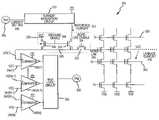
- FIG. 3is a schematic and block diagram of a leakage measurement system 300 for measuring leakage in the memory device 210 in accordance with one embodiment of the invention.
- a current generation circuit 310receives a current setting signal 308 from an input pad 302 and generates a reference current 312 at one of a number of current values based on the current setting signal 308 .
- the current generation circuit 310is connected in parallel to a number of measurement enable circuits 320 .
- the number of measurement enable circuits requiredis the number of the word lines (or, word lines and select gates, in another embodiment, where leakage on the select gates is to be measured as well) in the memory device 210 on which leakage current is to be measured; for example, N.
- the current generation circuit 310is connected in parallel to N measurement enable circuits 320 .
- FIG. 3only shows the current generation circuit 310 being connected to one of the N measurement enable circuits 320 .
- the reference current 312may be supplied to only the word line (or select gate) on which leakage is to be measured.
- the current generation circuit 310may be able to supply the same reference current to more than one word lines (and/or select gates), when leakage is measured on more than one word lines (and/or select gates) simultaneously, as the reference current 312 when leakage is measured on only one word line (or select gate).
- Each of the measurement enable circuits 320is connected to one of the word lines (and select gates, in an alternative embodiment) of the memory device 210 , and is also connected to one of N comparing circuits, comparing circuits 340 ( 1 ) through 340 (N).
- the outputs of the comparing circuits 340 ( 1 )- 340 (N)are received at a selection circuit 330 , which generates an output that is accessible externally through the output pad 380 .
- the current generation circuit 310includes a number of current mirrors that generate a number of reference currents from a master reference current. Since the operation and structure of current mirrors are well known in the art, in the interest of brevity the following description will focus on the other aspects of the present invention.
- each of the measurement enable circuits 320may enable the word line or select gate on which leakage current is measured by allowing the voltage level on the word line or select gate to be measured while a reference current is being supplied to the word line or select gate.
- the measurement enable circuit 320includes transistors 322 , 324 and 326 , each of which functions as a switch.
- the transistors 322 and 324may each be a n-type metal-oxide-semiconductor (NMOS) transistor, and the transistor 326 may be a p-type metal-oxide-semiconductor (PMOS) transistor.
- each of the transistors 322 , 324 and 326may be a switching circuit that is able to perform the functions described above.
- the transistorsare connected and arranged so that the aforementioned functionality of the measurement enable circuit 320 can be achieved.
- Each of the transistors 322 , 324 and 326has one control terminal (e.g., the gate) and two signal terminals (e.g., the source and drain), terminals A and B.
- the gatee.g., the gate
- signal terminalse.g., the source and drain
- terminal A of the transistor 322is connected to a corresponding word line 350
- terminal B of the transistor 322is connected to an input terminal of a corresponding comparing circuit.
- Terminal B of the transistor 322is also connected to terminal B of the transistor 324 as well as terminal B of the transistor 326 .
- the transistor 324is connected to the current generation circuit 310 at its terminal A.
- Terminal A of the transistor 326is connected to a voltage source that is at a predetermined voltage level.
- the predetermined voltage levelalthough shown to be Vcc in FIG. 3 , can be set to any voltage level other than Vcc, including 0 volt, as will be described in detail below.
- the control terminal of the transistor 322is connected to receive a “word line enable” signal 304 that may have either a high (enable) value or a low (disable) value.
- the control terminal of the transistor 324 and the control terminal of the transistor 326are not only connected to each other but also connected to receive a “measure enable” signal 306 , which may have either a high (enable) value or a low (disable) value.
- the transistors 322 and 324are chosen such that the transistors 322 and 324 are disabled when the signal on the control terminal is low, and enabled when the signal on the control terminal is high.
- the transistor 326is chosen such that it is enabled when the signal on its control terminal is low, and disabled when the signal is high.
- both the “word line enable” signal 304 and the “measure enable” signal 306are low.
- the timing of the changes in the “word line enable” signal 304 and the “measure enable” signal 306(e.g., going from low to high) is arranged such that the “word line enable” signal 304 goes high first, followed by a period of time, before the “measure enable” signal 306 goes high.
- the transistors 322 and 324are disabled while the transistor 326 is enabled.
- the predetermined voltage level at terminal A of the transistor 326(e.g., Vcc) is applied to the electrical line 328 that connects terminal B of the transistors 322 , 324 and 326 with one another and one of the inputs of the corresponding comparing circuit (e.g., 340 ( 1 )), and thereby sets the voltage on the electrical line 328 to be at the predetermined voltage level.
- both the transistor 322 and the transistor 324are enabled. With the transistor 322 enabled, the word line 350 is electrically coupled to the electrical line 328 , and the voltage levels on both are equalized. Since the voltage on the electrical line 328 has been previously set to the predetermined voltage level (e.g., Vcc), when the transistor 322 is enabled the voltage on the word line 350 is also set to the predetermined voltage level.
- the predetermined voltage levele.g., Vcc
- the “measure enable” signal 306goes high. This enables the transistor 324 and, at the same time, disables the transistor 326 . Consequently, the voltage source at terminal A of the transistor 326 is electrically decoupled from the electrical line 328 as well as the word line 350 . As such, any change in voltage level on the word line 350 and the electrical line 328 will be attributed to other factors, such as leakage. With the transistor 324 enabled, the current generation circuit 310 is electrically coupled to the electrical line 328 as well as the word line 350 .
- the reference current 312is supplied to the electrical line 328 as well as the word line 350 since the transistor 322 is still enabled.
- the current generation circuit 310utilizes a voltage source that is at a voltage level (e.g., HV or the power source of the memory device 210 ) higher than the predetermined voltage level (e.g., Vcc) that the word line 350 and the electrical line 328 were set to.
- the voltage level on the electrical line 328 and the word line 350may increase or decrease as the reference current 312 is being supplied to the electrical line 328 and the word line 350 . If the leakage current 370 on the word line 350 is smaller in magnitude than the current value of the reference current 312 , then the voltage level on the word line 350 (and on the electrical line 328 ) should rise because more electrical charges are being supplied than are leaking out. In contrast, if the leakage current 370 on the word line 350 is larger in magnitude than the current value of the reference current 312 , then the voltage level on the word line 350 (and on the electrical line 328 ) should fall because more electrical charges are leaking out than are being supplied.
- the comparing circuit 340 ( 1 )has a first input terminal 342 ( 1 ), connected to the electrical line 328 , and a second input terminal 344 ( 1 ), connected to the predetermined voltage level that is present at terminal A of the corresponding transistor 326 .
- the other comparing circuits 340 ( 2 )- 340 (N)are set up similarly, but for simplicity, only the connections of comparing circuit 340 ( 1 ) are shown.
- each of the comparing circuits 340 ( 1 )- 340 (N)is a comparator.
- each of the comparing circuits 340 ( 1 )- 340 (N)may be a circuit that is able to compare two values.
- each of the comparing circuits 340 ( 1 )- 340 (N)may be enabled to compare the voltage levels on its two input terminals at some time after the “measure enable” signal 306 went high from low, in order to allow sufficient time for the voltage level on the word line/select gate of interest to either rise or fall for more accurate measurement.
- the comparing circuit 340 ( 1 )When the voltage level on the word line 350 is higher than the predetermined voltage level, signifying the leakage current 370 is smaller than the reference current 312 , the comparing circuit 340 ( 1 ) generates an output signal indicating a PASS.
- the comparing circuit 340 ( 1 )generates an output signal indicating a FAIL.
- simultaneous leakage measurement on all the word lines as well as individual leakage measurement on each of the word linesare achievable. More specifically, a PASS/FAIL result representative of the results from the leakage measurement on all the N word lines may be accessible at the output pad 380 , and the individual PASS/FAIL result from the leakage measurement on each of the N word lines may also be accessible at the output pad 380 .
- the selection circuit 330may be a multiplexing logic circuit, the operation and structure of which are known in the art. In another embodiment, the selection circuit 330 may be a circuit that is able to perform the function described herein.
- the selection circuit 330receives the outputs of the comparing circuits 340 ( 1 )- 340 (N) and generates an output that is accessible externally through the output pad 380 .
- the selection circuit 330may include N NAND logic circuits each of which receiving the output of a corresponding comparing circuit.
- the result seen at the output pad 380will indicate a FAIL. This means that at least one of the word lines has an unacceptable leakage current compared to the reference current.
- the output of each of the comparing circuits 340 ( 1 )- 340 (N)may be connected to the output pad 380 by a transfer complementary metal-oxide-semiconductor (CMOS) logic, and thus the PASS/FAIL result for each of the N word lines may be individually seen at the output pad 380 .
- CMOScomplementary metal-oxide-semiconductor
- the selection of whether the type of leakage measurement is to be simultaneous leakage measurement or individual leakage measurementcan be made by initial setting. For example, the selection may be included in the “reference current setting” stage.
- the selection circuit 380can calculate or decode the outputs, based on the type of leakage measurement selected.
- the voltage level on its neighboring word linesmay or may not be different from the voltage on the particular word line.
- the voltage on the word line 350may be set to Vcc volt while the voltage on the neighboring word lines 355 and 360 is set to 0 volt. This is to help identify the direction of the leakage current.
- a particular word lineis set to Vcc volt and is measured to have huge leakage while the voltage on its neighboring word lines is also Vcc volt, the leakage is not likely a word line-to-word line leakage.
- the voltage that is applied to each of the word lines/select gates and one of the input terminals of the corresponding comparing circuitmay be set to a range of voltage levels.
- the voltage on all the word linesmay be set to Vcc.
- the voltage on the word linesmay be set to Vcc while the voltage on the select gates may be set to 0 volt.
- the voltage on the even-number word linesmay be set to Vcc while the voltage on the odd-number word lines may be set to 0 volt, or vice versa.
- the voltage on one word line or select gatemay be set to Vcc while the voltage on all the other word lines is set to 0 volt.
- the voltagemay be set to a voltage between Vcc and 0 (e.g., Vcc/2 or Vcc/3) in lieu of Vcc.
- Vccvoltage between Vcc and 0
- Vcc/2 or Vcc/3voltage between Vcc and 0
- FIG. 4is a timing diagram 400 that illustrates an example of the operation of the leakage measurement circuit of FIG. 3 with respect to one of the word lines of the memory device 210 .
- the signals and voltage levelstart out being low and 0 volt, respectively.
- the “word line enable” signalgoes high, allowing the word line (or select gate) of interest to be electrically coupled to a predetermined voltage level (e.g., Vcc).
- a predetermined voltage levele.g., Vcc
- the “measure enable” signalgoes high, removing the predetermined voltage level from the word line (or the select gate) and allowing the reference current to be supplied to the word line (or select gate).
- the voltage on the word line (or select gate)rises if the leakage current is smaller than the reference current, and the voltage on the word line (or select gate) falls if the leakage current is smaller than the reference current.
- the corresponding comparing circuitis enabled to compare the voltage on the word line (or select gate) with the predetermined voltage level that the word line (or select gate) was set to between times T 0 and T 1 .
- the comparing circuitthen generates an output indicating PASS if the voltage on the word line (or select gate) is greater than the predetermined voltage level. Or, the comparing circuit generates an output indicating FAIL if the voltage on the word line (or select gate) is less than the predetermined voltage level.
- the leakage measurement resultis available and accessible externally at the output pad 380 .
- a “discharge enable” signalstops the supply of the reference current to the word line (or select gate) and renders the voltage on the word line (or select gate) to be discharged so as to return the voltage on the word line (or select gate) to its initial voltage (e.g., 0 volt).
Landscapes
- For Increasing The Reliability Of Semiconductor Memories (AREA)
Abstract
Description
- This invention relates generally to memory devices, and more particularly, to leakage measurement in a memory device.
- With increasing popularity of electronic devices, such as laptop computers, portable digital assistants, digital cameras, mobile phones, digital audio players, video game consoles and the like, demand for nonvolatile memories are on the rise. Nonvolatile memories come in various types, including flash memories. Flash memories are widely used nowadays for fast information storage in electronic devices such as those mentioned above.
- In flash memories, data bits are stored in an array of individual memory cells, each of which includes a floating gate transistor. Generally speaking, each of the memory cells in a flash memory looks similar to a standard metal-oxide-semiconductor field-effect transistor (MOSFET), except that a flash memory cell has two gates instead of just one. One gate, the control gate, is analogous to the gate in a MOSFET. The other gate, the floating gate, is insulated all around by an oxide layer and is between the control gate and the substrate. Because the floating gate is insulated by its insulating oxide layer, any electrons placed on it get trapped there and thereby enable the storage of data. More specifically, when electrons are on the floating gate, their presence modifies, by partially canceling out, the electric field coming from the control gate. This results in the modification of the threshold voltage of the transistor, since a higher electric field is now required to enable an electrical current to flow between the source and the drain of the transistor than it would require without the electrons on the floating gate. If the number of electrons on the floating gate is sufficiently large, the resulting modified threshold voltage will be so high as to inhibit any electrical current to flow between the source and the drain when the normal operating voltage is applied to the control gate. Hence, in a typical flash memory cell that stores a binary bit, electrical current will either flow or not flow when a memory cell is being read by applying a voltage on the control gate, depending on the number of electrons on the floating gate. The flow or no flow of electrical current, in turn, translates to a
binary bit 1 or0, respectively. - In the pursuit of greater storage capacity in yet smaller chips, the flash memory density has been increasing over the years in accordance to the Moore's Law, largely due to the down scaling of the memory cell dimensions. The continued down scaling of MOS devices has created many challenges and opportunities, among them the formidable requirement for an ultra-thin gate oxide. One serious problem that comes along with thin oxide, and hinders further down scaling, is excessive leakage current. Specifically, when the oxide layer surrounding the floating gate of a flash memory cell is so thin that electrons stored on the floating gate may leak out (e.g., from the floating gate to the control gate and the word line that is coupled to the control gate, and eventually to ground), a result is that a binary bit0 originally stored in the memory cell might now appear to be a
binary bit 1. - Since the excessive leakage current for such an ultra-thin oxide will be unacceptable for very-large-scale integration (VLSI) applications, it is imperative that flash memories with unacceptable leakage current be identified during manufacturing process. As such, during manufacturing, flash memories are tested to assure that they are operating properly (e.g., having allowable leakage current). A leakage test is conducted to measure the leakage current on the word lines of each flash memory to determine whether the leakage current on any of the word lines is excessive and thus unacceptable.
- Conventionally, the leakage current in memory devices is measured using external leakage measurement instrument during the manufacturing process.
FIG. 1A illustrates a conventionalleakage measurement system 100 showing how the leakage current in a memory device, such as a flash memory, is measured. An externalleakage measurement instrument 120 is connected to aconventional memory device 110 viapad 130, which is connected torows decoder 140 in thememory device 110. Therows decoder 140 is coupled to the word lines of the memory device (not shown). The externalleakage measurement instrument 120 selects the word line on which the value of leakage current is measured by sending a selection signal torows decoder 140, which in turn selects the word line. FIG. 1B illustrates a conventionalleakage measurement system 105 for measuring the leakage current on one of the word lines of theconventional memory device 110 ofFIG. 1A . As shown,word line 150 is selected for leakage current measurement and is coupled to the externalleakage measurement instrument 120 viapad 130 androws decoder 140. Leakage paths of leakage current on a given word line may exist, for example, between a word line and another word line. One way to measure the leakage current on a given word line is to place on the word line a voltage that is different from the voltage on neighboring word lines. As a result, the voltage differential would induce leakage current to flow and thereby be detected and measured. Referring toFIG. 1B , whenword line 150 is at voltage Vcc and its neighboringword line 160 is at 0 volt, aleakage current 170 may flow fromword line 150 toword line 160, and is measured by the externalleakage measurement instrument 120.- However, this kind of leakage measurement takes longer time than ideal since leakage current is measured from outside of the memory devices. This results in long test time and leads to long manufacturing cycle, which translates into high cost of production. There is therefore a need for a way to reduce the test time required to measure leakage current on the word lines of memory devices such as flash memories.
- According to one aspect of the present invention, a memory device may include a leakage measurement circuit that is coupled to a plurality of word lines of the memory device. The leakage measurement circuit may be operable to generate a reference current and to determine whether a leakage current on one of the plurality of word lines is acceptable relative to the reference current.
- According to another aspect of the present invention, a method may include determining whether leakage on one of a plurality of word lines of a memory device is allowable using a circuit in the memory device.
FIG. 1A is a block diagram illustrating a conventional leakage measurement system for measuring leakage in a memory device.FIG. 1B is a schematic and block diagram illustrating a conventional leakage measurement system for measuring leakage current on a word line of a memory device.FIG. 2 is a block diagram illustrating a leakage measurement system in which a memory device has an internal leakage measurement circuit according to one embodiment of the invention.FIG. 3 is a schematic and block diagram illustrating measurement of leakage current on a plurality of word lines of a memory device using a leakage measurement circuit in the memory device according to one embodiment of the invention.FIG. 4 is a timing diagram illustrating the operation of the leakage measurement circuit ofFIG. 3 .- Described herein is a memory device and method for measuring leakage on the plurality of word lines in a memory device. The following description sets forth numerous specific details such as examples of specific systems, components, methods, and so forth, in order to provide a good understanding of several embodiments of the present invention. It will be apparent to one skilled in the art, however, that at least some embodiments of the present invention may be practiced without these specific details. In other instances, well-known components or methods are not described in detail or are presented in simple block diagram form in order to avoid unnecessarily obscuring the present invention. Thus, the specific details set forth are merely for illustration purpose. Particular implementations may vary from these illustration details and still be contemplated to be within the spirit and scope of the present invention.
- A
leakage measurement system 200 according to one embodiment of the invention is shown inFIG. 2 . Thememory device 210 ofFIG. 2 differs from thememory device 110 ofFIG. 1A by including aleakage measurement circuit 220. Theleakage measurement circuit 220 inmemory device 210 is coupled to the word lines (not shown) of thememory device 210. Theleakage measurement circuit 220 generates a reference current and determines whether a leakage current on each one of the word lines is acceptable relative to the reference current. - In one embodiment, the
leakage measurement circuit 220 in thememory device 210 may be able to generate a number of reference currents each at a current value different from the others. The leakage measurement circuit may receive an external signal for current setting through theinput pad 230. Based on the decoding of this external signal, theleakage measurement circuit 220 selects one of the number of reference currents to be used to run a leakage test on each of the word lines of thememory device 210. - By varying the current value of the reference current, leakage current on each of the word lines of the
memory device 210 can be measured. For example, theleakage measurement circuit 220 may initially generate a reference current at a current value of 2.5 μA, according to the current-setting external signal, and run a leakage test to determine whether the leakage on the word lines of thememory device 210 is acceptable. If, for example, the leakage test results indicate that the leakage current on each of the word lines of thememory device 210 is acceptable in comparison with the reference current (e.g., the leakage current on each of the word lines is less than 2.5 μA), a different external signal may be sent to theleakage measurement circuit 220 through theinput pad 230 so that theleakage measurement circuit 220 can generate a reference current at a different current value, say, 1 μA, and run another leakage test. In this example, if during this second leakage test the leakage current on one or more of the word lines of thememory device 210 is found to be unacceptable (e.g., more than 1 μA), theleakage measurement circuit 220 can thereby determine that the leakage current on the one or more of the word lines that failed the leakage test is between 1 μA and 2.5 μA. Meanwhile, the leakage current on each of all other word lines is less than 1 μA, since the leakage current on those word lines was found to be acceptable during the second leakage test using a reference current of 1 μA. - Accordingly, during manufacturing process the
memory device 210 may receive one or more external signals through theinput pad 230, and each of the one or more external signals may then initiate a leakage test on the word lines of thememory device 210 that runs at a different reference current value. At the end of each of the one or more leakage tests, theleakage measurement circuit 220 may generate a PASS/FAIL signal, which can be available at and accessible externally through an output pad, that indicates whether thememory device 210 has passed the particular leakage test. - In another embodiment, the
leakage measurement circuit 220 in thememory device 210 may automatically run a series of leakage tests, each of which uses a reference current generated at one current value that is different from the reference current values used in other leakage tests in the series of tests. For example, the series of leakage tests may begin with a relatively high current value for the reference current, and gradually decrease the current value for the reference current in each of the subsequent leakage test. Accordingly, when the series of leakage tests are completed, theleakage measurement circuit 220 will have measured the leakage current on each of the word lines of thememory device 210. Furthermore, the result of each of the series of tests can be accessible externally through an output pad. - Therefore, by incorporating a built-in circuit, such as the
leakage measurement circuit 220, in memory devices, the leakage current on the word lines of memory devices can be automatically measured without the use of an external leakage measurement instrument. Consequently, the manufacturing cycle and the overall product cost can be reduced. FIG. 3 is a schematic and block diagram of aleakage measurement system 300 for measuring leakage in thememory device 210 in accordance with one embodiment of the invention. As shown inFIG. 3 , acurrent generation circuit 310 receives acurrent setting signal 308 from aninput pad 302 and generates a reference current312 at one of a number of current values based on thecurrent setting signal 308. Thecurrent generation circuit 310 is connected in parallel to a number of measurement enablecircuits 320. The number of measurement enable circuits required is the number of the word lines (or, word lines and select gates, in another embodiment, where leakage on the select gates is to be measured as well) in thememory device 210 on which leakage current is to be measured; for example, N. In other words, thecurrent generation circuit 310 is connected in parallel to N measurement enablecircuits 320. For simplicity,FIG. 3 only shows thecurrent generation circuit 310 being connected to one of the N measurement enablecircuits 320. In one embodiment, the reference current312 may be supplied to only the word line (or select gate) on which leakage is to be measured. In an alternative embodiment, thecurrent generation circuit 310 may be able to supply the same reference current to more than one word lines (and/or select gates), when leakage is measured on more than one word lines (and/or select gates) simultaneously, as the reference current312 when leakage is measured on only one word line (or select gate).- Each of the measurement enable
circuits 320 is connected to one of the word lines (and select gates, in an alternative embodiment) of thememory device 210, and is also connected to one of N comparing circuits, comparing circuits340(1) through340(N). The outputs of the comparing circuits340(1)-340(N) are received at aselection circuit 330, which generates an output that is accessible externally through theoutput pad 380. In one embodiment, thecurrent generation circuit 310 includes a number of current mirrors that generate a number of reference currents from a master reference current. Since the operation and structure of current mirrors are well known in the art, in the interest of brevity the following description will focus on the other aspects of the present invention. - In one embodiment, each of the measurement enable
circuits 320 may enable the word line or select gate on which leakage current is measured by allowing the voltage level on the word line or select gate to be measured while a reference current is being supplied to the word line or select gate. As shown inFIG. 3 , the measurement enablecircuit 320 includestransistors 322,324 and326, each of which functions as a switch. In one embodiment, as shown inFIG. 3 , thetransistors 322 and324 may each be a n-type metal-oxide-semiconductor (NMOS) transistor, and the transistor326 may be a p-type metal-oxide-semiconductor (PMOS) transistor. In another embodiment, each of thetransistors 322,324 and326 may be a switching circuit that is able to perform the functions described above. The transistors are connected and arranged so that the aforementioned functionality of the measurement enablecircuit 320 can be achieved. Each of thetransistors 322,324 and326 has one control terminal (e.g., the gate) and two signal terminals (e.g., the source and drain), terminals A and B. When atransistor 322,324 or326 is enabled, electrical current can flow from one terminal to the other. Conversely, when atransistor 322,324 or326 is disabled, there is no current flow between its terminals. InFIG. 3 , terminal A of thetransistor 322 is connected to acorresponding word line 350, and terminal B of thetransistor 322 is connected to an input terminal of a corresponding comparing circuit. Terminal B of thetransistor 322 is also connected to terminal B of the transistor324 as well as terminal B of the transistor326. The transistor324 is connected to thecurrent generation circuit 310 at its terminal A. Terminal A of the transistor326 is connected to a voltage source that is at a predetermined voltage level. The predetermined voltage level, although shown to be Vcc inFIG. 3 , can be set to any voltage level other than Vcc, including 0 volt, as will be described in detail below. - The control terminal of the
transistor 322 is connected to receive a “word line enable” signal304 that may have either a high (enable) value or a low (disable) value. The control terminal of the transistor324 and the control terminal of the transistor326 are not only connected to each other but also connected to receive a “measure enable”signal 306, which may have either a high (enable) value or a low (disable) value. Thetransistors 322 and324 are chosen such that thetransistors 322 and324 are disabled when the signal on the control terminal is low, and enabled when the signal on the control terminal is high. Similarly, the transistor326 is chosen such that it is enabled when the signal on its control terminal is low, and disabled when the signal is high. - In operation, before a word line/select gate is selected for leakage measurement, both the “word line enable”
signal 304 and the “measure enable”signal 306 are low. In one embodiment, the timing of the changes in the “word line enable”signal 304 and the “measure enable” signal306 (e.g., going from low to high) is arranged such that the “word line enable”signal 304 goes high first, followed by a period of time, before the “measure enable”signal 306 goes high. When both the “word line enable”signal 304 and the “measure enable”signal 306 are low, thetransistors 322 and324 are disabled while the transistor326 is enabled. With the transistor326 enabled, the predetermined voltage level at terminal A of the transistor326 (e.g., Vcc) is applied to theelectrical line 328 that connects terminal B of thetransistors 322,324 and326 with one another and one of the inputs of the corresponding comparing circuit (e.g.,340(1)), and thereby sets the voltage on theelectrical line 328 to be at the predetermined voltage level. - When the “word line enable”
signal 304 goes high, both thetransistor 322 and the transistor324 are enabled. With thetransistor 322 enabled, theword line 350 is electrically coupled to theelectrical line 328, and the voltage levels on both are equalized. Since the voltage on theelectrical line 328 has been previously set to the predetermined voltage level (e.g., Vcc), when thetransistor 322 is enabled the voltage on theword line 350 is also set to the predetermined voltage level. - After a sufficient period of time that allows the voltage level on the
word line 350 to settle at the predetermined voltage level (e.g., Vcc), the “measure enable”signal 306 goes high. This enables the transistor324 and, at the same time, disables the transistor326. Consequently, the voltage source at terminal A of the transistor326 is electrically decoupled from theelectrical line 328 as well as theword line 350. As such, any change in voltage level on theword line 350 and theelectrical line 328 will be attributed to other factors, such as leakage. With the transistor324 enabled, thecurrent generation circuit 310 is electrically coupled to theelectrical line 328 as well as theword line 350. As a result, the reference current312 is supplied to theelectrical line 328 as well as theword line 350 since thetransistor 322 is still enabled. It should be noted that thecurrent generation circuit 310 utilizes a voltage source that is at a voltage level (e.g., HV or the power source of the memory device210) higher than the predetermined voltage level (e.g., Vcc) that theword line 350 and theelectrical line 328 were set to. - Depending on the size of the leakage current370 on the
word line 350, the voltage level on theelectrical line 328 and theword line 350 may increase or decrease as the reference current312 is being supplied to theelectrical line 328 and theword line 350. If the leakage current370 on theword line 350 is smaller in magnitude than the current value of the reference current312, then the voltage level on the word line350 (and on the electrical line328) should rise because more electrical charges are being supplied than are leaking out. In contrast, if the leakage current370 on theword line 350 is larger in magnitude than the current value of the reference current312, then the voltage level on the word line350 (and on the electrical line328) should fall because more electrical charges are leaking out than are being supplied. - As shown in
FIG. 3 , the comparing circuit340(1) has a first input terminal342(1), connected to theelectrical line 328, and a second input terminal344(1), connected to the predetermined voltage level that is present at terminal A of the corresponding transistor326. The other comparing circuits340(2)-340(N) are set up similarly, but for simplicity, only the connections of comparing circuit340(1) are shown. Each of the comparing circuits340(1)-340(N), therefore, compares the voltage level on its corresponding word line/select gate (which is electrically coupled to the electrical line that is physically connected to the first input terminal of the comparing circuit) with the predetermined voltage level that the word line/select gate was previously set to. In one embodiment, each of the comparing circuits340(1)-340(N) is a comparator. In another embodiment, each of the comparing circuits340(1)-340(N) may be a circuit that is able to compare two values. - In one embodiment, each of the comparing circuits340(1)-340(N) may be enabled to compare the voltage levels on its two input terminals at some time after the “measure enable” signal306 went high from low, in order to allow sufficient time for the voltage level on the word line/select gate of interest to either rise or fall for more accurate measurement. When the voltage level on the
word line 350 is higher than the predetermined voltage level, signifying the leakage current370 is smaller than the reference current312, the comparing circuit340(1) generates an output signal indicating a PASS. Likewise, when the voltage level on theword line 350 is lower than the predetermined voltage level, signifying the leakage current370 is larger than the reference current312, the comparing circuit340(1) generates an output signal indicating a FAIL. - According to one embodiment of the present invention, simultaneous leakage measurement on all the word lines as well as individual leakage measurement on each of the word lines are achievable. More specifically, a PASS/FAIL result representative of the results from the leakage measurement on all the N word lines may be accessible at the
output pad 380, and the individual PASS/FAIL result from the leakage measurement on each of the N word lines may also be accessible at theoutput pad 380. In one embodiment, theselection circuit 330 may be a multiplexing logic circuit, the operation and structure of which are known in the art. In another embodiment, theselection circuit 330 may be a circuit that is able to perform the function described herein. Theselection circuit 330 receives the outputs of the comparing circuits340(1)-340(N) and generates an output that is accessible externally through theoutput pad 380. For example, theselection circuit 330 may include N NAND logic circuits each of which receiving the output of a corresponding comparing circuit. In a simultaneous leakage measurement scenario, if one of the N word lines fails the leakage measurement at a given reference current value, the result seen at theoutput pad 380 will indicate a FAIL. This means that at least one of the word lines has an unacceptable leakage current compared to the reference current. Alternatively, in an individual leakage measurement scenario, the output of each of the comparing circuits340(1)-340(N) may be connected to theoutput pad 380 by a transfer complementary metal-oxide-semiconductor (CMOS) logic, and thus the PASS/FAIL result for each of the N word lines may be individually seen at theoutput pad 380. In one embodiment, the selection of whether the type of leakage measurement is to be simultaneous leakage measurement or individual leakage measurement can be made by initial setting. For example, the selection may be included in the “reference current setting” stage. Theselection circuit 380 can calculate or decode the outputs, based on the type of leakage measurement selected. - It should be appreciated by those skilled in the art that when leakage current is being measured on a particular word line the voltage level on its neighboring word lines may or may not be different from the voltage on the particular word line. For example, when the leakage current on
word line 350 is being measured, as shown inFIG. 3 , the voltage on theword line 350 may be set to Vcc volt while the voltage on the neighboringword lines FIG. 4 is a timing diagram400 that illustrates an example of the operation of the leakage measurement circuit ofFIG. 3 with respect to one of the word lines of thememory device 210. As shown, in one embodiment, initially the signals and voltage level start out being low and 0 volt, respectively. At time T0, the “word line enable” signal goes high, allowing the word line (or select gate) of interest to be electrically coupled to a predetermined voltage level (e.g., Vcc). At time T1, the voltage on the word line (or the select gate) has reached the predetermined voltage level. At time T2, the “measure enable” signal goes high, removing the predetermined voltage level from the word line (or the select gate) and allowing the reference current to be supplied to the word line (or select gate). As shown inFIG. 4 , the voltage on the word line (or select gate) rises if the leakage current is smaller than the reference current, and the voltage on the word line (or select gate) falls if the leakage current is smaller than the reference current. At time T3, the corresponding comparing circuit is enabled to compare the voltage on the word line (or select gate) with the predetermined voltage level that the word line (or select gate) was set to between times T0 and T1. The comparing circuit then generates an output indicating PASS if the voltage on the word line (or select gate) is greater than the predetermined voltage level. Or, the comparing circuit generates an output indicating FAIL if the voltage on the word line (or select gate) is less than the predetermined voltage level. At time T4 the leakage measurement result is available and accessible externally at theoutput pad 380. At time T5 a “discharge enable” signal stops the supply of the reference current to the word line (or select gate) and renders the voltage on the word line (or select gate) to be discharged so as to return the voltage on the word line (or select gate) to its initial voltage (e.g., 0 volt).- Thus, a circuit and method for measuring leakage on the plurality of word lines in a memory device have been described. It is to be understood that the above description is intended to be illustrative, and not restrictive. Many other embodiments will be apparent to those of skill in the art upon reading and understanding the above description. The scope of the invention should, therefore, be determined with reference to the appended claims, along with the full scope of equivalents to which such claims are entitled.
Claims (48)
Priority Applications (2)
| Application Number | Priority Date | Filing Date | Title |
|---|---|---|---|
| US12/271,140US9159452B2 (en) | 2008-11-14 | 2008-11-14 | Automatic word line leakage measurement circuitry |
| US14/857,305US9704542B2 (en) | 2008-11-14 | 2015-09-17 | Automatic word line leakage measurement circuitry |
Applications Claiming Priority (1)
| Application Number | Priority Date | Filing Date | Title |
|---|---|---|---|
| US12/271,140US9159452B2 (en) | 2008-11-14 | 2008-11-14 | Automatic word line leakage measurement circuitry |
Related Child Applications (1)
| Application Number | Title | Priority Date | Filing Date |
|---|---|---|---|
| US14/857,305DivisionUS9704542B2 (en) | 2008-11-14 | 2015-09-17 | Automatic word line leakage measurement circuitry |
Publications (2)
| Publication Number | Publication Date |
|---|---|
| US20100125429A1true US20100125429A1 (en) | 2010-05-20 |
| US9159452B2 US9159452B2 (en) | 2015-10-13 |
Family
ID=42172676
Family Applications (2)
| Application Number | Title | Priority Date | Filing Date |
|---|---|---|---|
| US12/271,140Active2031-01-14US9159452B2 (en) | 2008-11-14 | 2008-11-14 | Automatic word line leakage measurement circuitry |
| US14/857,305ActiveUS9704542B2 (en) | 2008-11-14 | 2015-09-17 | Automatic word line leakage measurement circuitry |
Family Applications After (1)
| Application Number | Title | Priority Date | Filing Date |
|---|---|---|---|
| US14/857,305ActiveUS9704542B2 (en) | 2008-11-14 | 2015-09-17 | Automatic word line leakage measurement circuitry |
Country Status (1)
| Country | Link |
|---|---|
| US (2) | US9159452B2 (en) |
Cited By (12)
| Publication number | Priority date | Publication date | Assignee | Title |
|---|---|---|---|---|
| US20110019487A1 (en)* | 2007-08-27 | 2011-01-27 | Macronix International Co., Ltd. | Apparatus and method for detecting word line leakage in memory devices |
| US20130271167A1 (en)* | 2011-11-23 | 2013-10-17 | Bharani Thiruvengadam | Current tests for i/o interface connectors |
| US8588007B2 (en) | 2011-02-28 | 2013-11-19 | Micron Technology, Inc. | Leakage measurement systems |
| US8634264B2 (en) | 2011-10-26 | 2014-01-21 | Micron Technology, Inc. | Apparatuses, integrated circuits, and methods for measuring leakage current |
| US9159452B2 (en) | 2008-11-14 | 2015-10-13 | Micron Technology, Inc. | Automatic word line leakage measurement circuitry |
| US9281078B2 (en)* | 2014-06-12 | 2016-03-08 | Micron Technology, Inc. | Program operations with embedded leak checks |
| US9842659B2 (en) | 2014-04-07 | 2017-12-12 | Samsung Electronics Co., Ltd. | Non-volatile memory device for detecting progressive error, memory system, and method of operating the non-volatile memory device |
| US9903901B2 (en) | 2014-07-15 | 2018-02-27 | Samsung Electronics Co., Ltd. | Leakage current detection device and nonvolatile memory device having the same |
| US11114178B1 (en)* | 2020-06-10 | 2021-09-07 | Western Digital Technologies, Inc. | Physical defect detection in an integrated memory assembly |
| US11404138B2 (en)* | 2020-06-18 | 2022-08-02 | Sandisk Technologies Llc | Non-volatile memory array leakage detection |
| US20240233850A1 (en)* | 2023-01-05 | 2024-07-11 | Samsung Electronics Co., Ltd. | Wordline defect detection circuit, wordline defect detection method, and memory device including the same |
| TWI881494B (en)* | 2023-10-16 | 2025-04-21 | 華邦電子股份有限公司 | Semiconductor memory device and testing method thereof |
Families Citing this family (4)
| Publication number | Priority date | Publication date | Assignee | Title |
|---|---|---|---|---|
| US20160254060A1 (en) | 2013-03-15 | 2016-09-01 | Taqua Wbh, Llc | High Speed And Low Power Sense Amplifier |
| KR20180135662A (en)* | 2017-06-13 | 2018-12-21 | 삼성전자주식회사 | Memory device, memory system and operating method of memory device |
| KR20230001805A (en) | 2021-06-29 | 2023-01-05 | 삼성전자주식회사 | Memory device configured to detect leakage current and operation method thereof |
| US12217815B2 (en)* | 2022-11-16 | 2025-02-04 | Nanya Technology Corporation | Memory testing system and memory testing method |
Citations (45)
| Publication number | Priority date | Publication date | Assignee | Title |
|---|---|---|---|---|
| US5117426A (en)* | 1990-03-26 | 1992-05-26 | Texas Instruments Incorporated | Circuit, device, and method to detect voltage leakage |
| US5258958A (en)* | 1989-06-12 | 1993-11-02 | Kabushiki Kaisha Toshiba | Semiconductor memory device |
| US5587948A (en)* | 1994-06-17 | 1996-12-24 | Kabushiki Kaisha Toshiba | Nonvolatile semiconductor memory with NAND structure memory arrays |
| US5600594A (en)* | 1994-03-31 | 1997-02-04 | Sgs-Thomson Microelectronics S.R.L. | Threshold voltage measuring device for memory cells |
| US5615154A (en)* | 1994-08-31 | 1997-03-25 | Fujitsu Limited | Flash memory device having erase verification |
| US5956277A (en)* | 1996-02-27 | 1999-09-21 | Micron Technology, Inc. | Circuit and method for performing tests on memory array cells using external sense amplifier reference current |
| US5966330A (en)* | 1998-04-30 | 1999-10-12 | Eon Silicon Devices, Inc. | Method and apparatus for measuring the threshold voltage of flash EEPROM memory cells being applied a variable control gate bias |
| US6205057B1 (en)* | 2000-02-15 | 2001-03-20 | Advanced Micro Devices | System and method for detecting flash memory threshold voltages |
| US6226200B1 (en)* | 1999-11-17 | 2001-05-01 | Motorola Inc. | In-circuit memory array bit cell threshold voltage distribution measurement |
| US6242936B1 (en)* | 1998-08-11 | 2001-06-05 | Texas Instruments Incorporated | Circuit for driving conductive line and testing conductive line for current leakage |
| US6285598B1 (en)* | 1997-03-06 | 2001-09-04 | Silicon Storage Technology, Inc. | Precision programming of nonvolatile memory cells |
| US6324094B1 (en)* | 1996-10-24 | 2001-11-27 | Micron Technology, Inc. | Apparatus for reading state of multistate non-volatile memory cells |
| US20020071314A1 (en)* | 1999-08-26 | 2002-06-13 | Mitsubishi Denki Kabushiki Kaisha | Nonvolatile semiconductor memory device capable of suppressing reduction of bit line potential in write-back operation and erase method |
| US20020118574A1 (en)* | 2001-02-26 | 2002-08-29 | Geoffrey Gongwer | Non-volatile memory with improved programming and method therefor |
| US6496415B2 (en)* | 2001-04-06 | 2002-12-17 | Integrated Memory Technologies, Inc. | Non-volatile memory device having high speed page mode operation |
| US6501674B2 (en)* | 2001-03-13 | 2002-12-31 | Oki Electric Industry Co., Ltd. | Semiconductor memory and its driving method |
| US6542409B2 (en)* | 2001-07-19 | 2003-04-01 | Fujitsu Limited | System for reference current tracking in a semiconductor device |
| US6580644B1 (en)* | 2001-05-31 | 2003-06-17 | Samusung Electronics Co., Ltd. | Flash memory device capable of checking memory cells for failure characteristics |
| US6639849B2 (en)* | 2002-02-28 | 2003-10-28 | Fujitsu Limited | Nonvolatile semiconductor memory device programming second dynamic reference cell according to threshold value of first dynamic reference cell |
| US6714453B2 (en)* | 2000-11-15 | 2004-03-30 | Stmicroelectronics Sa | Flash memory including means of checking memory cell threshold voltages |
| US6781884B2 (en)* | 2002-03-11 | 2004-08-24 | Fujitsu Limited | System for setting memory voltage threshold |
| US6819612B1 (en)* | 2003-03-13 | 2004-11-16 | Advanced Micro Devices, Inc. | Apparatus and method for a sense amplifier circuit that samples and holds a reference voltage |
| US6839279B2 (en)* | 2003-06-06 | 2005-01-04 | Fujitsu Limited | Nonvolatile semiconductor memory device |
| US20050105333A1 (en)* | 2003-11-18 | 2005-05-19 | Hynix Semiconductor Inc. | Method of measuring threshold voltage for a NAND flash memory device |
| US6912160B2 (en)* | 2003-03-11 | 2005-06-28 | Fujitsu Limited | Nonvolatile semiconductor memory device |
| US6975542B2 (en)* | 2003-05-08 | 2005-12-13 | Micron Technology, Inc. | NAND flash memory with improved read and verification threshold uniformity |
| US20060083070A1 (en)* | 2004-10-15 | 2006-04-20 | Matsushita Electric Industrial Co., Ltd. | Nonvolatile semiconductor memory |
| US7038482B1 (en)* | 2004-03-19 | 2006-05-02 | Cypress Semiconductor Corporation | Circuit and method for automatic measurement and compensation of transistor threshold voltage mismatch |
| US7180781B2 (en)* | 2003-10-08 | 2007-02-20 | Micron Technology, Inc. | Memory block erasing in a flash memory device |
| US20070216467A1 (en)* | 2006-03-14 | 2007-09-20 | Renesas Technology Corp. | Semiconductor device including internal voltage generation circuit |
| US7317658B2 (en)* | 2003-01-24 | 2008-01-08 | Renesas Technology Corp. | Semiconductor integrated circuit and IC card |
| US7397708B2 (en)* | 2005-08-03 | 2008-07-08 | Infineon Technologies Ag | Technique to suppress leakage current |
| US7483305B2 (en)* | 2006-08-28 | 2009-01-27 | Micron Technology, Inc. | Method, apparatus and system relating to automatic cell threshold voltage measurement |
| US7505334B1 (en)* | 2008-05-28 | 2009-03-17 | International Business Machines Corporation | Measurement method for reading multi-level memory cell utilizing measurement time delay as the characteristic parameter for level definition |
| US20090116290A1 (en)* | 2006-08-25 | 2009-05-07 | Micron Technology, Inc. | Methods and apparatuses relating to automatic cell threshold voltage measurement |
| US7619924B2 (en)* | 2006-08-30 | 2009-11-17 | Infineon Technologies Ag | Device and method for reading out memory information |
| US7672158B2 (en)* | 2004-04-15 | 2010-03-02 | Kabushiki Kaisha Toshiba | Non-volatile semiconductor memory device having non-selected word lines adjacent to selected word lines being charged at different timing for program disturb control |
| US20100238729A1 (en)* | 2009-03-23 | 2010-09-23 | Sanghyun Lee | Non-volatile memory with reduced leakage current for unselected blocks and method for operating same |
| US7835178B2 (en)* | 2007-08-27 | 2010-11-16 | Macronix International Co., Ltd. | Apparatus and method for detecting word line leakage in memory devices |
| US20100329026A1 (en)* | 2009-06-25 | 2010-12-30 | Mitsutoshi Nakamura | Semiconductor memory device with charge accumulation layer |
| US7898897B2 (en)* | 2008-06-30 | 2011-03-01 | Hynix Semiconductor Inc. | Circuit and method for generating word line off voltage |
| US7966577B2 (en)* | 2005-10-11 | 2011-06-21 | Apple Inc. | Multimedia control center |
| US20120218833A1 (en)* | 2011-02-28 | 2012-08-30 | Micron Technology, Inc. | Leakage measurement systems |
| US20120230107A1 (en)* | 2003-09-16 | 2012-09-13 | Renesas Electronics Corporation | Semiconductor memory device having memory block configuration |
| US20130107640A1 (en)* | 2011-10-26 | 2013-05-02 | Micron Technology, Inc. | Apparatuses, integrated circuits, and methods for measuring leakage current |
Family Cites Families (17)
| Publication number | Priority date | Publication date | Assignee | Title |
|---|---|---|---|---|
| US5428621A (en) | 1992-09-21 | 1995-06-27 | Sundisk Corporation | Latent defect handling in EEPROM devices |
| KR950008673B1 (en) | 1992-12-05 | 1995-08-04 | 삼성전자주식회사 | Wordline boosting and the same control circuit of semiconductor intergrated circuit |
| KR960006377B1 (en) | 1993-11-17 | 1996-05-15 | 삼성전자주식회사 | Word Line Loading Compensation Circuit of Semiconductor Memory Device |
| US6219290B1 (en) | 1998-10-14 | 2001-04-17 | Macronix International Co., Ltd. | Memory cell sense amplifier |
| KR100370234B1 (en)* | 1999-09-14 | 2003-01-29 | 삼성전자 주식회사 | Apparatus for detecting faulty cells in semiconductor memory and method therefor |
| US6639833B2 (en) | 2001-02-14 | 2003-10-28 | Stmicroelectronics S.R.L. | Method and circuit for dynamic reading of a memory cell at low supply voltage and with low output dynamics |
| US6977850B2 (en) | 2001-12-27 | 2005-12-20 | Kabushiki Kaisha Toshiba | Semiconductor device having switch circuit to supply voltage |
| JP2004055009A (en) | 2002-07-18 | 2004-02-19 | Renesas Technology Corp | Semiconductor memory module |
| US6868022B2 (en)* | 2003-03-28 | 2005-03-15 | Matrix Semiconductor, Inc. | Redundant memory structure using bad bit pointers |
| ITTO20070109A1 (en)* | 2007-02-14 | 2008-08-15 | St Microelectronics Srl | CIRCUIT AND READING METHOD FOR A NON-VOLATILE MEMORY DEVICE BASED ON THE ADAPTATIVE GENERATION OF AN ELECTRIC REFERENCE SIZE |
| US7515502B1 (en)* | 2007-09-18 | 2009-04-07 | International Business Machines Corporation | Memory array peripheral structures and use |
| US9159452B2 (en) | 2008-11-14 | 2015-10-13 | Micron Technology, Inc. | Automatic word line leakage measurement circuitry |
| TWI406290B (en) | 2009-06-26 | 2013-08-21 | Etron Technology Inc | Word line defect detecting device and method thereof |
| US8514630B2 (en) | 2010-07-09 | 2013-08-20 | Sandisk Technologies Inc. | Detection of word-line leakage in memory arrays: current based approach |
| US8432732B2 (en) | 2010-07-09 | 2013-04-30 | Sandisk Technologies Inc. | Detection of word-line leakage in memory arrays |
| US8379454B2 (en) | 2011-05-05 | 2013-02-19 | Sandisk Technologies Inc. | Detection of broken word-lines in memory arrays |
| US9437257B2 (en) | 2012-12-31 | 2016-09-06 | Taiwan Semiconductor Manufacturing Company, Ltd. | Sensing circuit, memory device and data detecting method |
- 2008
- 2008-11-14USUS12/271,140patent/US9159452B2/enactiveActive
- 2015
- 2015-09-17USUS14/857,305patent/US9704542B2/enactiveActive
Patent Citations (48)
| Publication number | Priority date | Publication date | Assignee | Title |
|---|---|---|---|---|
| US5258958A (en)* | 1989-06-12 | 1993-11-02 | Kabushiki Kaisha Toshiba | Semiconductor memory device |
| US5117426A (en)* | 1990-03-26 | 1992-05-26 | Texas Instruments Incorporated | Circuit, device, and method to detect voltage leakage |
| US5600594A (en)* | 1994-03-31 | 1997-02-04 | Sgs-Thomson Microelectronics S.R.L. | Threshold voltage measuring device for memory cells |
| US5587948A (en)* | 1994-06-17 | 1996-12-24 | Kabushiki Kaisha Toshiba | Nonvolatile semiconductor memory with NAND structure memory arrays |
| US5615154A (en)* | 1994-08-31 | 1997-03-25 | Fujitsu Limited | Flash memory device having erase verification |
| US5956277A (en)* | 1996-02-27 | 1999-09-21 | Micron Technology, Inc. | Circuit and method for performing tests on memory array cells using external sense amplifier reference current |
| US6324094B1 (en)* | 1996-10-24 | 2001-11-27 | Micron Technology, Inc. | Apparatus for reading state of multistate non-volatile memory cells |
| US6285598B1 (en)* | 1997-03-06 | 2001-09-04 | Silicon Storage Technology, Inc. | Precision programming of nonvolatile memory cells |
| US5966330A (en)* | 1998-04-30 | 1999-10-12 | Eon Silicon Devices, Inc. | Method and apparatus for measuring the threshold voltage of flash EEPROM memory cells being applied a variable control gate bias |
| US6242936B1 (en)* | 1998-08-11 | 2001-06-05 | Texas Instruments Incorporated | Circuit for driving conductive line and testing conductive line for current leakage |
| US20020071314A1 (en)* | 1999-08-26 | 2002-06-13 | Mitsubishi Denki Kabushiki Kaisha | Nonvolatile semiconductor memory device capable of suppressing reduction of bit line potential in write-back operation and erase method |
| US6226200B1 (en)* | 1999-11-17 | 2001-05-01 | Motorola Inc. | In-circuit memory array bit cell threshold voltage distribution measurement |
| US6205057B1 (en)* | 2000-02-15 | 2001-03-20 | Advanced Micro Devices | System and method for detecting flash memory threshold voltages |
| US6714453B2 (en)* | 2000-11-15 | 2004-03-30 | Stmicroelectronics Sa | Flash memory including means of checking memory cell threshold voltages |
| US20020118574A1 (en)* | 2001-02-26 | 2002-08-29 | Geoffrey Gongwer | Non-volatile memory with improved programming and method therefor |
| US6501674B2 (en)* | 2001-03-13 | 2002-12-31 | Oki Electric Industry Co., Ltd. | Semiconductor memory and its driving method |
| US6496415B2 (en)* | 2001-04-06 | 2002-12-17 | Integrated Memory Technologies, Inc. | Non-volatile memory device having high speed page mode operation |
| US6580644B1 (en)* | 2001-05-31 | 2003-06-17 | Samusung Electronics Co., Ltd. | Flash memory device capable of checking memory cells for failure characteristics |
| US6542409B2 (en)* | 2001-07-19 | 2003-04-01 | Fujitsu Limited | System for reference current tracking in a semiconductor device |
| US6639849B2 (en)* | 2002-02-28 | 2003-10-28 | Fujitsu Limited | Nonvolatile semiconductor memory device programming second dynamic reference cell according to threshold value of first dynamic reference cell |
| US6781884B2 (en)* | 2002-03-11 | 2004-08-24 | Fujitsu Limited | System for setting memory voltage threshold |
| US7317658B2 (en)* | 2003-01-24 | 2008-01-08 | Renesas Technology Corp. | Semiconductor integrated circuit and IC card |
| US6912160B2 (en)* | 2003-03-11 | 2005-06-28 | Fujitsu Limited | Nonvolatile semiconductor memory device |
| US6819612B1 (en)* | 2003-03-13 | 2004-11-16 | Advanced Micro Devices, Inc. | Apparatus and method for a sense amplifier circuit that samples and holds a reference voltage |
| US6975542B2 (en)* | 2003-05-08 | 2005-12-13 | Micron Technology, Inc. | NAND flash memory with improved read and verification threshold uniformity |
| US6839279B2 (en)* | 2003-06-06 | 2005-01-04 | Fujitsu Limited | Nonvolatile semiconductor memory device |
| US20120230107A1 (en)* | 2003-09-16 | 2012-09-13 | Renesas Electronics Corporation | Semiconductor memory device having memory block configuration |
| US7180781B2 (en)* | 2003-10-08 | 2007-02-20 | Micron Technology, Inc. | Memory block erasing in a flash memory device |
| US7031210B2 (en)* | 2003-11-18 | 2006-04-18 | Hynix Semiconductor Inc. | Method of measuring threshold voltage for a NAND flash memory device |
| US20050105333A1 (en)* | 2003-11-18 | 2005-05-19 | Hynix Semiconductor Inc. | Method of measuring threshold voltage for a NAND flash memory device |
| US7038482B1 (en)* | 2004-03-19 | 2006-05-02 | Cypress Semiconductor Corporation | Circuit and method for automatic measurement and compensation of transistor threshold voltage mismatch |
| US7672158B2 (en)* | 2004-04-15 | 2010-03-02 | Kabushiki Kaisha Toshiba | Non-volatile semiconductor memory device having non-selected word lines adjacent to selected word lines being charged at different timing for program disturb control |
| US20060083070A1 (en)* | 2004-10-15 | 2006-04-20 | Matsushita Electric Industrial Co., Ltd. | Nonvolatile semiconductor memory |
| US7397708B2 (en)* | 2005-08-03 | 2008-07-08 | Infineon Technologies Ag | Technique to suppress leakage current |
| US7966577B2 (en)* | 2005-10-11 | 2011-06-21 | Apple Inc. | Multimedia control center |
| US20070216467A1 (en)* | 2006-03-14 | 2007-09-20 | Renesas Technology Corp. | Semiconductor device including internal voltage generation circuit |
| US20090116290A1 (en)* | 2006-08-25 | 2009-05-07 | Micron Technology, Inc. | Methods and apparatuses relating to automatic cell threshold voltage measurement |
| US7483305B2 (en)* | 2006-08-28 | 2009-01-27 | Micron Technology, Inc. | Method, apparatus and system relating to automatic cell threshold voltage measurement |
| US7619924B2 (en)* | 2006-08-30 | 2009-11-17 | Infineon Technologies Ag | Device and method for reading out memory information |
| US7835178B2 (en)* | 2007-08-27 | 2010-11-16 | Macronix International Co., Ltd. | Apparatus and method for detecting word line leakage in memory devices |
| US7505334B1 (en)* | 2008-05-28 | 2009-03-17 | International Business Machines Corporation | Measurement method for reading multi-level memory cell utilizing measurement time delay as the characteristic parameter for level definition |
| US7898897B2 (en)* | 2008-06-30 | 2011-03-01 | Hynix Semiconductor Inc. | Circuit and method for generating word line off voltage |
| US20100238729A1 (en)* | 2009-03-23 | 2010-09-23 | Sanghyun Lee | Non-volatile memory with reduced leakage current for unselected blocks and method for operating same |
| US20100329026A1 (en)* | 2009-06-25 | 2010-12-30 | Mitsutoshi Nakamura | Semiconductor memory device with charge accumulation layer |
| US20120218833A1 (en)* | 2011-02-28 | 2012-08-30 | Micron Technology, Inc. | Leakage measurement systems |
| US20140071772A1 (en)* | 2011-02-28 | 2014-03-13 | Micron Technology, Inc. | Leakage measurement systems |
| US20130107640A1 (en)* | 2011-10-26 | 2013-05-02 | Micron Technology, Inc. | Apparatuses, integrated circuits, and methods for measuring leakage current |
| US20140133249A1 (en)* | 2011-10-26 | 2014-05-15 | Micron Technology, Inc. | Apparatuses, integrated circuits, and methods for measuring leakage current |
Cited By (24)
| Publication number | Priority date | Publication date | Assignee | Title |
|---|---|---|---|---|
| US20110019487A1 (en)* | 2007-08-27 | 2011-01-27 | Macronix International Co., Ltd. | Apparatus and method for detecting word line leakage in memory devices |
| US8018772B2 (en)* | 2007-08-27 | 2011-09-13 | Macronix International Co., Ltd. | Apparatus and method for detecting word line leakage in memory devices |
| US9704542B2 (en) | 2008-11-14 | 2017-07-11 | Micron Technology, Inc. | Automatic word line leakage measurement circuitry |
| US9159452B2 (en) | 2008-11-14 | 2015-10-13 | Micron Technology, Inc. | Automatic word line leakage measurement circuitry |
| US8588007B2 (en) | 2011-02-28 | 2013-11-19 | Micron Technology, Inc. | Leakage measurement systems |
| US8947946B2 (en) | 2011-02-28 | 2015-02-03 | Micron Technology, Inc. | Leakage measurement systems |
| US9269410B2 (en) | 2011-02-28 | 2016-02-23 | Micron Technology, Inc. | Leakage measurement systems |
| US8634264B2 (en) | 2011-10-26 | 2014-01-21 | Micron Technology, Inc. | Apparatuses, integrated circuits, and methods for measuring leakage current |
| US8867290B2 (en) | 2011-10-26 | 2014-10-21 | Micron Technology, Inc. | Apparatuses, integrated circuits, and methods for measuring leakage current |
| US20150029802A1 (en)* | 2011-10-26 | 2015-01-29 | Micron Technology, Inc. | Apparatuses, integrated circuits, and methods for measuring leakage current |
| US9183948B2 (en)* | 2011-10-26 | 2015-11-10 | Micron Technology, Inc. | Apparatuses, integrated circuits, and methods for measuring leakage current |
| US9551741B2 (en)* | 2011-11-23 | 2017-01-24 | Intel Corporation | Current tests for I/O interface connectors |
| US20130271167A1 (en)* | 2011-11-23 | 2013-10-17 | Bharani Thiruvengadam | Current tests for i/o interface connectors |
| US9842659B2 (en) | 2014-04-07 | 2017-12-12 | Samsung Electronics Co., Ltd. | Non-volatile memory device for detecting progressive error, memory system, and method of operating the non-volatile memory device |
| US9281078B2 (en)* | 2014-06-12 | 2016-03-08 | Micron Technology, Inc. | Program operations with embedded leak checks |
| US9761322B2 (en) | 2014-06-12 | 2017-09-12 | Micron Technology, Inc. | Program operations with embedded leak checks |
| US10366767B2 (en) | 2014-06-12 | 2019-07-30 | Micron Technology, Inc. | Memory devices configured to perform leak checks |
| US10665307B2 (en) | 2014-06-12 | 2020-05-26 | Micron Technology, Inc. | Memory devices configured to perform leak checks |
| US9903901B2 (en) | 2014-07-15 | 2018-02-27 | Samsung Electronics Co., Ltd. | Leakage current detection device and nonvolatile memory device having the same |
| US11114178B1 (en)* | 2020-06-10 | 2021-09-07 | Western Digital Technologies, Inc. | Physical defect detection in an integrated memory assembly |
| US11404138B2 (en)* | 2020-06-18 | 2022-08-02 | Sandisk Technologies Llc | Non-volatile memory array leakage detection |
| US20240233850A1 (en)* | 2023-01-05 | 2024-07-11 | Samsung Electronics Co., Ltd. | Wordline defect detection circuit, wordline defect detection method, and memory device including the same |
| EP4398253A3 (en)* | 2023-01-05 | 2024-08-07 | Samsung Electronics Co., Ltd. | Wordline defect detection circuit, wordline defect detection method, and memory device including the same |
| TWI881494B (en)* | 2023-10-16 | 2025-04-21 | 華邦電子股份有限公司 | Semiconductor memory device and testing method thereof |
Also Published As
| Publication number | Publication date |
|---|---|
| US20160005471A1 (en) | 2016-01-07 |
| US9704542B2 (en) | 2017-07-11 |
| US9159452B2 (en) | 2015-10-13 |
Similar Documents
| Publication | Publication Date | Title |
|---|---|---|
| US9704542B2 (en) | Automatic word line leakage measurement circuitry | |
| US9269410B2 (en) | Leakage measurement systems | |
| US9183948B2 (en) | Apparatuses, integrated circuits, and methods for measuring leakage current | |
| US8847221B2 (en) | Stacked semiconductor device and method of testing the same | |
| US8358545B2 (en) | Semiconductor memory | |
| US9281076B2 (en) | Semiconductor device | |
| KR102520496B1 (en) | One-time programmable(otp) memory device and method of testing otp memory device | |
| TWI659424B (en) | Non-volatile semiconductor memory device and reading method thereof | |
| US20130043889A1 (en) | Capacitance evaluation apparatuses and methods | |
| US20100054071A1 (en) | Semiconductor memory device | |
| US20220301634A1 (en) | Memory device read operations | |
| US7826268B2 (en) | Nonvolatile semiconductor memory | |
| US6903976B2 (en) | Semiconductor memory device reduced in power consumption during burn-in test | |
| US11557341B2 (en) | Memory array structures and methods for determination of resistive characteristics of access lines | |
| US7541612B2 (en) | Multi-chip package semiconductor device and method of detecting a failure thereof | |
| US6949953B2 (en) | Method and apparatus for providing a preselected voltage to test or repair a semiconductor device | |
| US9406384B2 (en) | Matching semiconductor circuits | |
| JPH0684387A (en) | Semiconductor storage device | |
| JP2025146208A (en) | Non-volatile memory device | |
| JP2616678B2 (en) | Dynamic ROM data read circuit | |
| KR19990024439A (en) | Semiconductor memory device having a function of measuring word line enable potential | |
| JP2010027096A (en) | Memory circuit device and data read-out method |
Legal Events
| Date | Code | Title | Description |
|---|---|---|---|
| AS | Assignment | Owner name:MICRON TECHNOLOGY, INC.,IDAHO Free format text:ASSIGNMENT OF ASSIGNORS INTEREST;ASSIGNOR:YAMADA, SHIGEKAZU;REEL/FRAME:021835/0525 Effective date:20081031 Owner name:MICRON TECHNOLOGY, INC., IDAHO Free format text:ASSIGNMENT OF ASSIGNORS INTEREST;ASSIGNOR:YAMADA, SHIGEKAZU;REEL/FRAME:021835/0525 Effective date:20081031 | |
| FEPP | Fee payment procedure | Free format text:PAYOR NUMBER ASSIGNED (ORIGINAL EVENT CODE: ASPN); ENTITY STATUS OF PATENT OWNER: LARGE ENTITY | |
| STCF | Information on status: patent grant | Free format text:PATENTED CASE | |
| AS | Assignment | Owner name:U.S. BANK NATIONAL ASSOCIATION, AS COLLATERAL AGENT, CALIFORNIA Free format text:SECURITY INTEREST;ASSIGNOR:MICRON TECHNOLOGY, INC.;REEL/FRAME:038669/0001 Effective date:20160426 Owner name:U.S. BANK NATIONAL ASSOCIATION, AS COLLATERAL AGEN Free format text:SECURITY INTEREST;ASSIGNOR:MICRON TECHNOLOGY, INC.;REEL/FRAME:038669/0001 Effective date:20160426 | |
| AS | Assignment | Owner name:MORGAN STANLEY SENIOR FUNDING, INC., AS COLLATERAL AGENT, MARYLAND Free format text:PATENT SECURITY AGREEMENT;ASSIGNOR:MICRON TECHNOLOGY, INC.;REEL/FRAME:038954/0001 Effective date:20160426 Owner name:MORGAN STANLEY SENIOR FUNDING, INC., AS COLLATERAL Free format text:PATENT SECURITY AGREEMENT;ASSIGNOR:MICRON TECHNOLOGY, INC.;REEL/FRAME:038954/0001 Effective date:20160426 | |
| AS | Assignment | Owner name:U.S. BANK NATIONAL ASSOCIATION, AS COLLATERAL AGENT, CALIFORNIA Free format text:CORRECTIVE ASSIGNMENT TO CORRECT THE REPLACE ERRONEOUSLY FILED PATENT #7358718 WITH THE CORRECT PATENT #7358178 PREVIOUSLY RECORDED ON REEL 038669 FRAME 0001. ASSIGNOR(S) HEREBY CONFIRMS THE SECURITY INTEREST;ASSIGNOR:MICRON TECHNOLOGY, INC.;REEL/FRAME:043079/0001 Effective date:20160426 Owner name:U.S. BANK NATIONAL ASSOCIATION, AS COLLATERAL AGEN Free format text:CORRECTIVE ASSIGNMENT TO CORRECT THE REPLACE ERRONEOUSLY FILED PATENT #7358718 WITH THE CORRECT PATENT #7358178 PREVIOUSLY RECORDED ON REEL 038669 FRAME 0001. ASSIGNOR(S) HEREBY CONFIRMS THE SECURITY INTEREST;ASSIGNOR:MICRON TECHNOLOGY, INC.;REEL/FRAME:043079/0001 Effective date:20160426 | |
| AS | Assignment | Owner name:JPMORGAN CHASE BANK, N.A., AS COLLATERAL AGENT, ILLINOIS Free format text:SECURITY INTEREST;ASSIGNORS:MICRON TECHNOLOGY, INC.;MICRON SEMICONDUCTOR PRODUCTS, INC.;REEL/FRAME:047540/0001 Effective date:20180703 Owner name:JPMORGAN CHASE BANK, N.A., AS COLLATERAL AGENT, IL Free format text:SECURITY INTEREST;ASSIGNORS:MICRON TECHNOLOGY, INC.;MICRON SEMICONDUCTOR PRODUCTS, INC.;REEL/FRAME:047540/0001 Effective date:20180703 | |
| AS | Assignment | Owner name:MICRON TECHNOLOGY, INC., IDAHO Free format text:RELEASE BY SECURED PARTY;ASSIGNOR:U.S. BANK NATIONAL ASSOCIATION, AS COLLATERAL AGENT;REEL/FRAME:047243/0001 Effective date:20180629 | |
| MAFP | Maintenance fee payment | Free format text:PAYMENT OF MAINTENANCE FEE, 4TH YEAR, LARGE ENTITY (ORIGINAL EVENT CODE: M1551); ENTITY STATUS OF PATENT OWNER: LARGE ENTITY Year of fee payment:4 | |
| AS | Assignment | Owner name:MICRON TECHNOLOGY, INC., IDAHO Free format text:RELEASE BY SECURED PARTY;ASSIGNOR:MORGAN STANLEY SENIOR FUNDING, INC., AS COLLATERAL AGENT;REEL/FRAME:050937/0001 Effective date:20190731 | |
| AS | Assignment | Owner name:MICRON SEMICONDUCTOR PRODUCTS, INC., IDAHO Free format text:RELEASE BY SECURED PARTY;ASSIGNOR:JPMORGAN CHASE BANK, N.A., AS COLLATERAL AGENT;REEL/FRAME:051028/0001 Effective date:20190731 Owner name:MICRON TECHNOLOGY, INC., IDAHO Free format text:RELEASE BY SECURED PARTY;ASSIGNOR:JPMORGAN CHASE BANK, N.A., AS COLLATERAL AGENT;REEL/FRAME:051028/0001 Effective date:20190731 | |
| MAFP | Maintenance fee payment | Free format text:PAYMENT OF MAINTENANCE FEE, 8TH YEAR, LARGE ENTITY (ORIGINAL EVENT CODE: M1552); ENTITY STATUS OF PATENT OWNER: LARGE ENTITY Year of fee payment:8 |