US20100123227A1 - Integrated circuit packaging system with increased connectivity and method of manufacture thereof - Google Patents
Integrated circuit packaging system with increased connectivity and method of manufacture thereofDownload PDFInfo
- Publication number
- US20100123227A1 US20100123227A1US12/272,765US27276508AUS2010123227A1US 20100123227 A1US20100123227 A1US 20100123227A1US 27276508 AUS27276508 AUS 27276508AUS 2010123227 A1US2010123227 A1US 2010123227A1
- Authority
- US
- United States
- Prior art keywords
- integrated circuit
- contact pads
- forming
- package
- connection leads
- Prior art date
- Legal status (The legal status is an assumption and is not a legal conclusion. Google has not performed a legal analysis and makes no representation as to the accuracy of the status listed.)
- Granted
Links
Images


Classifications
- H—ELECTRICITY
- H01—ELECTRIC ELEMENTS
- H01L—SEMICONDUCTOR DEVICES NOT COVERED BY CLASS H10
- H01L23/00—Details of semiconductor or other solid state devices
- H01L23/28—Encapsulations, e.g. encapsulating layers, coatings, e.g. for protection
- H01L23/31—Encapsulations, e.g. encapsulating layers, coatings, e.g. for protection characterised by the arrangement or shape
- H01L23/3107—Encapsulations, e.g. encapsulating layers, coatings, e.g. for protection characterised by the arrangement or shape the device being completely enclosed
- H—ELECTRICITY
- H01—ELECTRIC ELEMENTS
- H01L—SEMICONDUCTOR DEVICES NOT COVERED BY CLASS H10
- H01L21/00—Processes or apparatus adapted for the manufacture or treatment of semiconductor or solid state devices or of parts thereof
- H01L21/02—Manufacture or treatment of semiconductor devices or of parts thereof
- H01L21/04—Manufacture or treatment of semiconductor devices or of parts thereof the devices having potential barriers, e.g. a PN junction, depletion layer or carrier concentration layer
- H01L21/50—Assembly of semiconductor devices using processes or apparatus not provided for in a single one of the groups H01L21/18 - H01L21/326 or H10D48/04 - H10D48/07 e.g. sealing of a cap to a base of a container
- H01L21/56—Encapsulations, e.g. encapsulation layers, coatings
- H01L21/565—Moulds
- H—ELECTRICITY
- H01—ELECTRIC ELEMENTS
- H01L—SEMICONDUCTOR DEVICES NOT COVERED BY CLASS H10
- H01L23/00—Details of semiconductor or other solid state devices
- H01L23/48—Arrangements for conducting electric current to or from the solid state body in operation, e.g. leads, terminal arrangements ; Selection of materials therefor
- H01L23/488—Arrangements for conducting electric current to or from the solid state body in operation, e.g. leads, terminal arrangements ; Selection of materials therefor consisting of soldered or bonded constructions
- H01L23/495—Lead-frames or other flat leads
- H01L23/49503—Lead-frames or other flat leads characterised by the die pad
- H01L23/4951—Chip-on-leads or leads-on-chip techniques, i.e. inner lead fingers being used as die pad
- H—ELECTRICITY
- H01—ELECTRIC ELEMENTS
- H01L—SEMICONDUCTOR DEVICES NOT COVERED BY CLASS H10
- H01L23/00—Details of semiconductor or other solid state devices
- H01L23/48—Arrangements for conducting electric current to or from the solid state body in operation, e.g. leads, terminal arrangements ; Selection of materials therefor
- H01L23/488—Arrangements for conducting electric current to or from the solid state body in operation, e.g. leads, terminal arrangements ; Selection of materials therefor consisting of soldered or bonded constructions
- H01L23/495—Lead-frames or other flat leads
- H01L23/49541—Geometry of the lead-frame
- H01L23/49548—Cross section geometry
- H01L23/49551—Cross section geometry characterised by bent parts
- H—ELECTRICITY
- H01—ELECTRIC ELEMENTS
- H01L—SEMICONDUCTOR DEVICES NOT COVERED BY CLASS H10
- H01L23/00—Details of semiconductor or other solid state devices
- H01L23/48—Arrangements for conducting electric current to or from the solid state body in operation, e.g. leads, terminal arrangements ; Selection of materials therefor
- H01L23/488—Arrangements for conducting electric current to or from the solid state body in operation, e.g. leads, terminal arrangements ; Selection of materials therefor consisting of soldered or bonded constructions
- H01L23/495—Lead-frames or other flat leads
- H01L23/49572—Lead-frames or other flat leads consisting of thin flexible metallic tape with or without a film carrier
- H—ELECTRICITY
- H01—ELECTRIC ELEMENTS
- H01L—SEMICONDUCTOR DEVICES NOT COVERED BY CLASS H10
- H01L23/00—Details of semiconductor or other solid state devices
- H01L23/48—Arrangements for conducting electric current to or from the solid state body in operation, e.g. leads, terminal arrangements ; Selection of materials therefor
- H01L23/488—Arrangements for conducting electric current to or from the solid state body in operation, e.g. leads, terminal arrangements ; Selection of materials therefor consisting of soldered or bonded constructions
- H01L23/495—Lead-frames or other flat leads
- H01L23/49575—Assemblies of semiconductor devices on lead frames
- H—ELECTRICITY
- H01—ELECTRIC ELEMENTS
- H01L—SEMICONDUCTOR DEVICES NOT COVERED BY CLASS H10
- H01L25/00—Assemblies consisting of a plurality of semiconductor or other solid state devices
- H01L25/03—Assemblies consisting of a plurality of semiconductor or other solid state devices all the devices being of a type provided for in a single subclass of subclasses H10B, H10D, H10F, H10H, H10K or H10N, e.g. assemblies of rectifier diodes
- H01L25/10—Assemblies consisting of a plurality of semiconductor or other solid state devices all the devices being of a type provided for in a single subclass of subclasses H10B, H10D, H10F, H10H, H10K or H10N, e.g. assemblies of rectifier diodes the devices having separate containers
- H01L25/105—Assemblies consisting of a plurality of semiconductor or other solid state devices all the devices being of a type provided for in a single subclass of subclasses H10B, H10D, H10F, H10H, H10K or H10N, e.g. assemblies of rectifier diodes the devices having separate containers the devices being integrated devices of class H10
- H—ELECTRICITY
- H01—ELECTRIC ELEMENTS
- H01L—SEMICONDUCTOR DEVICES NOT COVERED BY CLASS H10
- H01L2224/00—Indexing scheme for arrangements for connecting or disconnecting semiconductor or solid-state bodies and methods related thereto as covered by H01L24/00
- H01L2224/01—Means for bonding being attached to, or being formed on, the surface to be connected, e.g. chip-to-package, die-attach, "first-level" interconnects; Manufacturing methods related thereto
- H01L2224/02—Bonding areas; Manufacturing methods related thereto
- H01L2224/04—Structure, shape, material or disposition of the bonding areas prior to the connecting process
- H01L2224/04042—Bonding areas specifically adapted for wire connectors, e.g. wirebond pads
- H—ELECTRICITY
- H01—ELECTRIC ELEMENTS
- H01L—SEMICONDUCTOR DEVICES NOT COVERED BY CLASS H10
- H01L2224/00—Indexing scheme for arrangements for connecting or disconnecting semiconductor or solid-state bodies and methods related thereto as covered by H01L24/00
- H01L2224/01—Means for bonding being attached to, or being formed on, the surface to be connected, e.g. chip-to-package, die-attach, "first-level" interconnects; Manufacturing methods related thereto
- H01L2224/02—Bonding areas; Manufacturing methods related thereto
- H01L2224/04—Structure, shape, material or disposition of the bonding areas prior to the connecting process
- H01L2224/05—Structure, shape, material or disposition of the bonding areas prior to the connecting process of an individual bonding area
- H01L2224/0554—External layer
- H01L2224/0555—Shape
- H01L2224/05552—Shape in top view
- H01L2224/05554—Shape in top view being square
- H—ELECTRICITY
- H01—ELECTRIC ELEMENTS
- H01L—SEMICONDUCTOR DEVICES NOT COVERED BY CLASS H10
- H01L2224/00—Indexing scheme for arrangements for connecting or disconnecting semiconductor or solid-state bodies and methods related thereto as covered by H01L24/00
- H01L2224/01—Means for bonding being attached to, or being formed on, the surface to be connected, e.g. chip-to-package, die-attach, "first-level" interconnects; Manufacturing methods related thereto
- H01L2224/02—Bonding areas; Manufacturing methods related thereto
- H01L2224/04—Structure, shape, material or disposition of the bonding areas prior to the connecting process
- H01L2224/05—Structure, shape, material or disposition of the bonding areas prior to the connecting process of an individual bonding area
- H01L2224/0554—External layer
- H01L2224/0556—Disposition
- H01L2224/0557—Disposition the external layer being disposed on a via connection of the semiconductor or solid-state body
- H—ELECTRICITY
- H01—ELECTRIC ELEMENTS
- H01L—SEMICONDUCTOR DEVICES NOT COVERED BY CLASS H10
- H01L2224/00—Indexing scheme for arrangements for connecting or disconnecting semiconductor or solid-state bodies and methods related thereto as covered by H01L24/00
- H01L2224/01—Means for bonding being attached to, or being formed on, the surface to be connected, e.g. chip-to-package, die-attach, "first-level" interconnects; Manufacturing methods related thereto
- H01L2224/02—Bonding areas; Manufacturing methods related thereto
- H01L2224/04—Structure, shape, material or disposition of the bonding areas prior to the connecting process
- H01L2224/05—Structure, shape, material or disposition of the bonding areas prior to the connecting process of an individual bonding area
- H01L2224/0554—External layer
- H01L2224/0556—Disposition
- H01L2224/05571—Disposition the external layer being disposed in a recess of the surface
- H—ELECTRICITY
- H01—ELECTRIC ELEMENTS
- H01L—SEMICONDUCTOR DEVICES NOT COVERED BY CLASS H10
- H01L2224/00—Indexing scheme for arrangements for connecting or disconnecting semiconductor or solid-state bodies and methods related thereto as covered by H01L24/00
- H01L2224/01—Means for bonding being attached to, or being formed on, the surface to be connected, e.g. chip-to-package, die-attach, "first-level" interconnects; Manufacturing methods related thereto
- H01L2224/02—Bonding areas; Manufacturing methods related thereto
- H01L2224/04—Structure, shape, material or disposition of the bonding areas prior to the connecting process
- H01L2224/05—Structure, shape, material or disposition of the bonding areas prior to the connecting process of an individual bonding area
- H01L2224/0554—External layer
- H01L2224/05573—Single external layer
- H—ELECTRICITY
- H01—ELECTRIC ELEMENTS
- H01L—SEMICONDUCTOR DEVICES NOT COVERED BY CLASS H10
- H01L2224/00—Indexing scheme for arrangements for connecting or disconnecting semiconductor or solid-state bodies and methods related thereto as covered by H01L24/00
- H01L2224/01—Means for bonding being attached to, or being formed on, the surface to be connected, e.g. chip-to-package, die-attach, "first-level" interconnects; Manufacturing methods related thereto
- H01L2224/02—Bonding areas; Manufacturing methods related thereto
- H01L2224/04—Structure, shape, material or disposition of the bonding areas prior to the connecting process
- H01L2224/06—Structure, shape, material or disposition of the bonding areas prior to the connecting process of a plurality of bonding areas
- H01L2224/061—Disposition
- H01L2224/0612—Layout
- H01L2224/0615—Mirror array, i.e. array having only a reflection symmetry, i.e. bilateral symmetry
- H—ELECTRICITY
- H01—ELECTRIC ELEMENTS
- H01L—SEMICONDUCTOR DEVICES NOT COVERED BY CLASS H10
- H01L2224/00—Indexing scheme for arrangements for connecting or disconnecting semiconductor or solid-state bodies and methods related thereto as covered by H01L24/00
- H01L2224/01—Means for bonding being attached to, or being formed on, the surface to be connected, e.g. chip-to-package, die-attach, "first-level" interconnects; Manufacturing methods related thereto
- H01L2224/10—Bump connectors; Manufacturing methods related thereto
- H01L2224/15—Structure, shape, material or disposition of the bump connectors after the connecting process
- H01L2224/16—Structure, shape, material or disposition of the bump connectors after the connecting process of an individual bump connector
- H01L2224/161—Disposition
- H01L2224/16151—Disposition the bump connector connecting between a semiconductor or solid-state body and an item not being a semiconductor or solid-state body, e.g. chip-to-substrate, chip-to-passive
- H01L2224/16221—Disposition the bump connector connecting between a semiconductor or solid-state body and an item not being a semiconductor or solid-state body, e.g. chip-to-substrate, chip-to-passive the body and the item being stacked
- H01L2224/16245—Disposition the bump connector connecting between a semiconductor or solid-state body and an item not being a semiconductor or solid-state body, e.g. chip-to-substrate, chip-to-passive the body and the item being stacked the item being metallic
- H—ELECTRICITY
- H01—ELECTRIC ELEMENTS
- H01L—SEMICONDUCTOR DEVICES NOT COVERED BY CLASS H10
- H01L2224/00—Indexing scheme for arrangements for connecting or disconnecting semiconductor or solid-state bodies and methods related thereto as covered by H01L24/00
- H01L2224/01—Means for bonding being attached to, or being formed on, the surface to be connected, e.g. chip-to-package, die-attach, "first-level" interconnects; Manufacturing methods related thereto
- H01L2224/26—Layer connectors, e.g. plate connectors, solder or adhesive layers; Manufacturing methods related thereto
- H01L2224/31—Structure, shape, material or disposition of the layer connectors after the connecting process
- H01L2224/32—Structure, shape, material or disposition of the layer connectors after the connecting process of an individual layer connector
- H01L2224/321—Disposition
- H01L2224/32135—Disposition the layer connector connecting between different semiconductor or solid-state bodies, i.e. chip-to-chip
- H01L2224/32145—Disposition the layer connector connecting between different semiconductor or solid-state bodies, i.e. chip-to-chip the bodies being stacked
- H—ELECTRICITY
- H01—ELECTRIC ELEMENTS
- H01L—SEMICONDUCTOR DEVICES NOT COVERED BY CLASS H10
- H01L2224/00—Indexing scheme for arrangements for connecting or disconnecting semiconductor or solid-state bodies and methods related thereto as covered by H01L24/00
- H01L2224/01—Means for bonding being attached to, or being formed on, the surface to be connected, e.g. chip-to-package, die-attach, "first-level" interconnects; Manufacturing methods related thereto
- H01L2224/26—Layer connectors, e.g. plate connectors, solder or adhesive layers; Manufacturing methods related thereto
- H01L2224/31—Structure, shape, material or disposition of the layer connectors after the connecting process
- H01L2224/32—Structure, shape, material or disposition of the layer connectors after the connecting process of an individual layer connector
- H01L2224/321—Disposition
- H01L2224/32151—Disposition the layer connector connecting between a semiconductor or solid-state body and an item not being a semiconductor or solid-state body, e.g. chip-to-substrate, chip-to-passive
- H01L2224/32221—Disposition the layer connector connecting between a semiconductor or solid-state body and an item not being a semiconductor or solid-state body, e.g. chip-to-substrate, chip-to-passive the body and the item being stacked
- H01L2224/32245—Disposition the layer connector connecting between a semiconductor or solid-state body and an item not being a semiconductor or solid-state body, e.g. chip-to-substrate, chip-to-passive the body and the item being stacked the item being metallic
- H—ELECTRICITY
- H01—ELECTRIC ELEMENTS
- H01L—SEMICONDUCTOR DEVICES NOT COVERED BY CLASS H10
- H01L2224/00—Indexing scheme for arrangements for connecting or disconnecting semiconductor or solid-state bodies and methods related thereto as covered by H01L24/00
- H01L2224/01—Means for bonding being attached to, or being formed on, the surface to be connected, e.g. chip-to-package, die-attach, "first-level" interconnects; Manufacturing methods related thereto
- H01L2224/42—Wire connectors; Manufacturing methods related thereto
- H01L2224/47—Structure, shape, material or disposition of the wire connectors after the connecting process
- H01L2224/48—Structure, shape, material or disposition of the wire connectors after the connecting process of an individual wire connector
- H01L2224/4805—Shape
- H01L2224/4809—Loop shape
- H01L2224/48091—Arched
- H—ELECTRICITY
- H01—ELECTRIC ELEMENTS
- H01L—SEMICONDUCTOR DEVICES NOT COVERED BY CLASS H10
- H01L2224/00—Indexing scheme for arrangements for connecting or disconnecting semiconductor or solid-state bodies and methods related thereto as covered by H01L24/00
- H01L2224/01—Means for bonding being attached to, or being formed on, the surface to be connected, e.g. chip-to-package, die-attach, "first-level" interconnects; Manufacturing methods related thereto
- H01L2224/42—Wire connectors; Manufacturing methods related thereto
- H01L2224/47—Structure, shape, material or disposition of the wire connectors after the connecting process
- H01L2224/48—Structure, shape, material or disposition of the wire connectors after the connecting process of an individual wire connector
- H01L2224/481—Disposition
- H01L2224/48135—Connecting between different semiconductor or solid-state bodies, i.e. chip-to-chip
- H01L2224/48145—Connecting between different semiconductor or solid-state bodies, i.e. chip-to-chip the bodies being stacked
- H—ELECTRICITY
- H01—ELECTRIC ELEMENTS
- H01L—SEMICONDUCTOR DEVICES NOT COVERED BY CLASS H10
- H01L2224/00—Indexing scheme for arrangements for connecting or disconnecting semiconductor or solid-state bodies and methods related thereto as covered by H01L24/00
- H01L2224/01—Means for bonding being attached to, or being formed on, the surface to be connected, e.g. chip-to-package, die-attach, "first-level" interconnects; Manufacturing methods related thereto
- H01L2224/42—Wire connectors; Manufacturing methods related thereto
- H01L2224/47—Structure, shape, material or disposition of the wire connectors after the connecting process
- H01L2224/48—Structure, shape, material or disposition of the wire connectors after the connecting process of an individual wire connector
- H01L2224/481—Disposition
- H01L2224/48151—Connecting between a semiconductor or solid-state body and an item not being a semiconductor or solid-state body, e.g. chip-to-substrate, chip-to-passive
- H01L2224/48221—Connecting between a semiconductor or solid-state body and an item not being a semiconductor or solid-state body, e.g. chip-to-substrate, chip-to-passive the body and the item being stacked
- H01L2224/48245—Connecting between a semiconductor or solid-state body and an item not being a semiconductor or solid-state body, e.g. chip-to-substrate, chip-to-passive the body and the item being stacked the item being metallic
- H01L2224/48247—Connecting between a semiconductor or solid-state body and an item not being a semiconductor or solid-state body, e.g. chip-to-substrate, chip-to-passive the body and the item being stacked the item being metallic connecting the wire to a bond pad of the item
- H—ELECTRICITY
- H01—ELECTRIC ELEMENTS
- H01L—SEMICONDUCTOR DEVICES NOT COVERED BY CLASS H10
- H01L2224/00—Indexing scheme for arrangements for connecting or disconnecting semiconductor or solid-state bodies and methods related thereto as covered by H01L24/00
- H01L2224/01—Means for bonding being attached to, or being formed on, the surface to be connected, e.g. chip-to-package, die-attach, "first-level" interconnects; Manufacturing methods related thereto
- H01L2224/42—Wire connectors; Manufacturing methods related thereto
- H01L2224/47—Structure, shape, material or disposition of the wire connectors after the connecting process
- H01L2224/49—Structure, shape, material or disposition of the wire connectors after the connecting process of a plurality of wire connectors
- H01L2224/491—Disposition
- H01L2224/4912—Layout
- H01L2224/49171—Fan-out arrangements
- H—ELECTRICITY
- H01—ELECTRIC ELEMENTS
- H01L—SEMICONDUCTOR DEVICES NOT COVERED BY CLASS H10
- H01L2224/00—Indexing scheme for arrangements for connecting or disconnecting semiconductor or solid-state bodies and methods related thereto as covered by H01L24/00
- H01L2224/73—Means for bonding being of different types provided for in two or more of groups H01L2224/10, H01L2224/18, H01L2224/26, H01L2224/34, H01L2224/42, H01L2224/50, H01L2224/63, H01L2224/71
- H01L2224/732—Location after the connecting process
- H01L2224/73201—Location after the connecting process on the same surface
- H01L2224/73215—Layer and wire connectors
- H—ELECTRICITY
- H01—ELECTRIC ELEMENTS
- H01L—SEMICONDUCTOR DEVICES NOT COVERED BY CLASS H10
- H01L2224/00—Indexing scheme for arrangements for connecting or disconnecting semiconductor or solid-state bodies and methods related thereto as covered by H01L24/00
- H01L2224/73—Means for bonding being of different types provided for in two or more of groups H01L2224/10, H01L2224/18, H01L2224/26, H01L2224/34, H01L2224/42, H01L2224/50, H01L2224/63, H01L2224/71
- H01L2224/732—Location after the connecting process
- H01L2224/73251—Location after the connecting process on different surfaces
- H01L2224/73265—Layer and wire connectors
- H—ELECTRICITY
- H01—ELECTRIC ELEMENTS
- H01L—SEMICONDUCTOR DEVICES NOT COVERED BY CLASS H10
- H01L2225/00—Details relating to assemblies covered by the group H01L25/00 but not provided for in its subgroups
- H01L2225/03—All the devices being of a type provided for in the same main group of the same subclass of class H10, e.g. assemblies of rectifier diodes
- H01L2225/10—All the devices being of a type provided for in the same main group of the same subclass of class H10, e.g. assemblies of rectifier diodes the devices having separate containers
- H01L2225/1005—All the devices being of a type provided for in the same main group of the same subclass of class H10, e.g. assemblies of rectifier diodes the devices having separate containers the devices being integrated devices of class H10
- H01L2225/1011—All the devices being of a type provided for in the same main group of the same subclass of class H10, e.g. assemblies of rectifier diodes the devices having separate containers the devices being integrated devices of class H10 the containers being in a stacked arrangement
- H01L2225/1017—All the devices being of a type provided for in the same main group of the same subclass of class H10, e.g. assemblies of rectifier diodes the devices having separate containers the devices being integrated devices of class H10 the containers being in a stacked arrangement the lowermost container comprising a device support
- H01L2225/1029—All the devices being of a type provided for in the same main group of the same subclass of class H10, e.g. assemblies of rectifier diodes the devices having separate containers the devices being integrated devices of class H10 the containers being in a stacked arrangement the lowermost container comprising a device support the support being a lead frame
- H—ELECTRICITY
- H01—ELECTRIC ELEMENTS
- H01L—SEMICONDUCTOR DEVICES NOT COVERED BY CLASS H10
- H01L2225/00—Details relating to assemblies covered by the group H01L25/00 but not provided for in its subgroups
- H01L2225/03—All the devices being of a type provided for in the same main group of the same subclass of class H10, e.g. assemblies of rectifier diodes
- H01L2225/10—All the devices being of a type provided for in the same main group of the same subclass of class H10, e.g. assemblies of rectifier diodes the devices having separate containers
- H01L2225/1005—All the devices being of a type provided for in the same main group of the same subclass of class H10, e.g. assemblies of rectifier diodes the devices having separate containers the devices being integrated devices of class H10
- H01L2225/1011—All the devices being of a type provided for in the same main group of the same subclass of class H10, e.g. assemblies of rectifier diodes the devices having separate containers the devices being integrated devices of class H10 the containers being in a stacked arrangement
- H01L2225/1047—Details of electrical connections between containers
- H01L2225/1058—Bump or bump-like electrical connections, e.g. balls, pillars, posts
- H—ELECTRICITY
- H01—ELECTRIC ELEMENTS
- H01L—SEMICONDUCTOR DEVICES NOT COVERED BY CLASS H10
- H01L2225/00—Details relating to assemblies covered by the group H01L25/00 but not provided for in its subgroups
- H01L2225/03—All the devices being of a type provided for in the same main group of the same subclass of class H10, e.g. assemblies of rectifier diodes
- H01L2225/10—All the devices being of a type provided for in the same main group of the same subclass of class H10, e.g. assemblies of rectifier diodes the devices having separate containers
- H01L2225/1005—All the devices being of a type provided for in the same main group of the same subclass of class H10, e.g. assemblies of rectifier diodes the devices having separate containers the devices being integrated devices of class H10
- H01L2225/1011—All the devices being of a type provided for in the same main group of the same subclass of class H10, e.g. assemblies of rectifier diodes the devices having separate containers the devices being integrated devices of class H10 the containers being in a stacked arrangement
- H01L2225/1094—Thermal management, e.g. cooling
- H—ELECTRICITY
- H01—ELECTRIC ELEMENTS
- H01L—SEMICONDUCTOR DEVICES NOT COVERED BY CLASS H10
- H01L24/00—Arrangements for connecting or disconnecting semiconductor or solid-state bodies; Methods or apparatus related thereto
- H01L24/01—Means for bonding being attached to, or being formed on, the surface to be connected, e.g. chip-to-package, die-attach, "first-level" interconnects; Manufacturing methods related thereto
- H01L24/02—Bonding areas ; Manufacturing methods related thereto
- H01L24/04—Structure, shape, material or disposition of the bonding areas prior to the connecting process
- H01L24/05—Structure, shape, material or disposition of the bonding areas prior to the connecting process of an individual bonding area
- H—ELECTRICITY
- H01—ELECTRIC ELEMENTS
- H01L—SEMICONDUCTOR DEVICES NOT COVERED BY CLASS H10
- H01L24/00—Arrangements for connecting or disconnecting semiconductor or solid-state bodies; Methods or apparatus related thereto
- H01L24/01—Means for bonding being attached to, or being formed on, the surface to be connected, e.g. chip-to-package, die-attach, "first-level" interconnects; Manufacturing methods related thereto
- H01L24/42—Wire connectors; Manufacturing methods related thereto
- H01L24/47—Structure, shape, material or disposition of the wire connectors after the connecting process
- H01L24/48—Structure, shape, material or disposition of the wire connectors after the connecting process of an individual wire connector
- H—ELECTRICITY
- H01—ELECTRIC ELEMENTS
- H01L—SEMICONDUCTOR DEVICES NOT COVERED BY CLASS H10
- H01L24/00—Arrangements for connecting or disconnecting semiconductor or solid-state bodies; Methods or apparatus related thereto
- H01L24/01—Means for bonding being attached to, or being formed on, the surface to be connected, e.g. chip-to-package, die-attach, "first-level" interconnects; Manufacturing methods related thereto
- H01L24/42—Wire connectors; Manufacturing methods related thereto
- H01L24/47—Structure, shape, material or disposition of the wire connectors after the connecting process
- H01L24/49—Structure, shape, material or disposition of the wire connectors after the connecting process of a plurality of wire connectors
- H—ELECTRICITY
- H01—ELECTRIC ELEMENTS
- H01L—SEMICONDUCTOR DEVICES NOT COVERED BY CLASS H10
- H01L2924/00—Indexing scheme for arrangements or methods for connecting or disconnecting semiconductor or solid-state bodies as covered by H01L24/00
- H01L2924/0001—Technical content checked by a classifier
- H01L2924/00014—Technical content checked by a classifier the subject-matter covered by the group, the symbol of which is combined with the symbol of this group, being disclosed without further technical details
- H—ELECTRICITY
- H01—ELECTRIC ELEMENTS
- H01L—SEMICONDUCTOR DEVICES NOT COVERED BY CLASS H10
- H01L2924/00—Indexing scheme for arrangements or methods for connecting or disconnecting semiconductor or solid-state bodies as covered by H01L24/00
- H01L2924/10—Details of semiconductor or other solid state devices to be connected
- H01L2924/11—Device type
- H01L2924/14—Integrated circuits
- H—ELECTRICITY
- H01—ELECTRIC ELEMENTS
- H01L—SEMICONDUCTOR DEVICES NOT COVERED BY CLASS H10
- H01L2924/00—Indexing scheme for arrangements or methods for connecting or disconnecting semiconductor or solid-state bodies as covered by H01L24/00
- H01L2924/15—Details of package parts other than the semiconductor or other solid state devices to be connected
- H01L2924/181—Encapsulation
Definitions
- the present inventionrelates generally to an integrated circuit packaging system, and more particularly to a system for packaging multiple integrated circuits in a leaded package.
- Integrated circuit diceare conventionally enclosed in plastic packages that provide protection from hostile environments and enable electrical interconnection between the integrated circuit die and an underlying substrate such as a printed circuit board (PCB).
- the elements of such a packageinclude a conductive lead frame, an integrated circuit die, bonding material to attach the integrated circuit die to the lead frame, bond wires which electrically connect pads on the integrated circuit die to individual leads of the lead frame, and a hard plastic encapsulant material which covers the other components and forms the exterior of the package.
- the lead frameis the central supporting structure of such a package.
- a portion of the lead frameis internal to the package, i.e., completely surrounded by the plastic encapsulant. Portions of the leads of the lead frame extend externally from the package or are partially exposed within the encapsulant material for use in electrically connecting the package to another component. In certain semiconductor packages, a portion of the die pad of the lead frame also remains exposed within the exterior of the package for use as a heat sink.
- a typical QFP packagecomprises a thin, generally square package body defining four peripheral sides of substantially equal length. Protruding from each of the four peripheral sides of the package body are a number of leads which each have a generally gull-wing configuration. Portions of the leads are internal to the package body, and are electrically connected to respective ones of the pads or terminals of a semiconductor die also encapsulated within the package body. The semiconductor die is itself mounted to a die pad of the QFP package lead frame.
- the present inventionprovides a method of manufacture of an integrated circuit packaging system including: forming a lead frame having contact pads and connection leads; coupling a base integrated circuit to the contact pads; coupling a chip interconnect between the base integrated circuit, the connection leads, the contact pads, or a combination thereof; molding a package body, on the lead frame, the base integrated circuit, and the chip interconnects, includes having the contact pads exposed; and forming a bottom surface on the package body including forming the connection leads to be coplanar with the bottom surface.
- the present inventionprovides an integrated circuit packaging system includes a package body having contact pads and connection leads exposed; a base integrated circuit coupled to the contact pads; chip interconnects between the base integrated circuit, the connection leads, the contact pads, or a combination thereof; and a bottom surface on the package body with the connection leads formed coplanar to the bottom surface.
- FIG. 1is a cross-sectional view of an integrated circuit packaging system with increased connectivity, as viewed along the section line 1 - 1 of FIG. 3 , in an embodiment of the present invention.
- FIG. 2is a top plan view of a lead frame assembly segment for implementing the integrated circuit packaging system of the present invention.
- FIG. 3is a bottom view of the integrated circuit packaging system of FIG. 1 .
- FIG. 4is a cross-sectional view, substantially similar to FIG. 1 , of a package stack application using an alternative embodiment of the integrated circuit packaging system.
- FIG. 5is a bottom view of an integrated circuit packaging system, in a second alternative embodiment of the present invention.
- FIG. 6is a cross-sectional view of the integrated circuit packaging system, along a section line 6 - 6 , of FIG. 5 .
- FIG. 7is a top plan view of a lead frame assembly segment for implementing the integrated circuit packaging system of FIG. 5 .
- FIG. 8is a cross-sectional view, substantially similar to FIG. 6 , of an integrated circuit packaging system, in a third alternative embodiment of the present invention.
- FIG. 9is a top plan view of a lead frame assembly segment for implementing the integrated circuit packaging system of FIG. 8 .
- FIG. 10is a cross-sectional view, substantially similar to FIG. 6 , of an integrated circuit packaging system, in a fourth alternative embodiment of the present invention.
- FIG. 11is a cross-sectional view, substantially similar to FIG. 6 , of an integrated circuit packaging system, in a fifth alternative embodiment of the present invention.
- FIG. 12is a cross-sectional view, substantially similar to FIG. 6 , of a package stack application using an alternative embodiment of the integrated circuit packaging system, of FIG. 10 .
- FIG. 13is a cross-sectional view, substantially similar to FIG. 6 , of an integrated circuit packaging system, in a sixth alternative embodiment of the present invention.
- FIG. 14is a cross-sectional view, substantially similar to FIG. 6 , of an integrated circuit packaging system, in a seventh alternative embodiment of the present invention.
- FIG. 15is a cross-sectional view, substantially similar to FIG. 6 , of an integrated circuit packaging system, in an eighth alternative embodiment of the present invention.
- FIG. 16is a cross-sectional view, substantially similar to FIG. 6 , of an integrated circuit packaging system, in a ninth alternative embodiment of the present invention.
- FIG. 17is a flow chart of a method of manufacture of an integrated circuit packaging system in an embodiment of the present invention.
- the term “horizontal” as used hereinis defined as a plane parallel to the plane or surface of the integrated circuit die, regardless of its orientation.
- the term “vertical”refers to a direction perpendicular to the horizontal as just defined. Terms, such as “above”, “below”, “bottom”, “top”, “side” (as in “sidewall”), “higher”, “lower”, “upper”, “over”, and “under”, are defined with respect to the horizontal plane.
- the term “on”means there is direct contact among elements.
- processingas used herein includes stamping, forging, patterning, exposure, development, etching, cleaning, and/or removal of the material or laser trimming as required in forming a described structure.
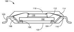
- FIG. 1therein is shown a cross-sectional view of an integrated circuit packaging system 100 with increased connectivity, as viewed along the section line 1 - 1 of FIG. 3 , in an embodiment of the present invention.
- the cross-sectional view of the integrated circuit packaging system 100depicts a base integrated circuit 102 coupled to contact pads 104 by chip interconnects 106 , such as bond wires, solder balls, solder bumps, solder columns, or stud bumps.
- the contact pads 104may extend from a tie bar 108 that may elevate to a level near that of the inactive side of the base integrated circuit 102 , such as a flip chip integrated circuit.
- a wire bond integrated circuit 110may be attached to the inactive side of the base integrated circuit 102 by an adhesive 112 , such as a die attach material. Electrical interconnects 114 , such as bond wires, may couple the wire bond integrated circuit 110 to a bond finger 116 , the tie bar 108 , or a combination thereof.
- a package body 118may be formed on the base integrated circuit 102 , the chip interconnects 106 , the wire bond integrated circuit 110 , the electrical interconnects 114 , the tie bars 108 , the bond fingers 116 , and the contact pads 104 .
- the package body 118may be formed by injecting an epoxy molding compound that leaves a portion of the contact pads 104 exposed on the bottom surface.
- Connection leads 120may extend from the bond finger 116 , beyond the package body 118 , and are bent to be coplanar with a bottom surface 122 of the package body.
- the connection leads 120may be formed so that they are coplanar with the exposed portion of the contact pads 104 and the bottom surface 122 of the package body 118 .
- the integrated circuit packaging system 100may provide a significantly increased input/output capacity, multiple chip integration, and ease of assembly, without increasing the thickness of the package. This aspect can assist in the integration of dissimilar technologies such as memory and sequential logic integrated circuits.
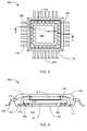
- FIG. 2therein is shown a top plan view of a lead frame assembly 200 segment for implementing the integrated circuit packaging system of the present invention.
- the top plan view of the lead frame assembly 200depicts a lead frame 202 , having a dam bar 204 that joins the connection leads 120 , the bond fingers 116 , and the tie bars 108 prior to molding the package body 118 , of FIG. 1 .
- the base integrated circuit 102may be positioned over the contact pads 104 and coupled by the chip interconnects 106 .
- the wire bond integrated circuit 110is attached to the base integrated circuit 102 by the adhesive 112 . While the wire bond integrated circuit 110 is shown to be smaller than the base integrated circuit 102 , this is an example only and the actual size of the wire bond integrated circuit 110 may differ.
- the electrical interconnects 114are shown coupled between a bonding pad 206 and the bond finger 116 or the tie bar 108 . This is also by way of an example and the bonding pad 206 may be coupled to the bond finger 116 , the tie bar 108 , or the combination thereof. By coupling the bonding pad 206 to the tie bar 108 , a signal may be shared between the base integrated circuit 102 and the wire bond integrated circuit 110 without the addition of interconnects outside the package body 118 .
- the dam bar 204may provide a sealing surface during the formation of the package body 118 , of FIG. 1 .
- the dam bar 204may be removed, in a subsequent manufacturing step, once the package body 118 is formed to hold the tie bars 108 and the bond fingers 116 in place.
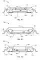
- FIG. 3therein is shown a bottom view of the integrated circuit packaging system 100 of FIG. 1 .
- the bottom view of the integrated circuit packaging system 100depicts the contact pads 104 positioned around a package bottom 302 of the package body 118 .
- the number and position of the contact pads 104is an example only and the actual number and position may differ. While the package body 118 is shown having sloped edges on the package bottom 302 , this is an example only.
- connection leads 120may be distributed along a package side 304 .
- the number of the connection leads 120 on the package side 304may be equal for each of the sides. This configuration matches the definition of an industry standard quad flat pack (QFP) package.
- QFPquad flat pack
- the number and position of the connection leads 120 formed on the package side 304is an example only and the actual position and number may differ as long as all of the package sides 304 are the same.
- the section line 1 - 1shows the position and viewing direction of the cross-sectional view of FIG. 1 .
- connection leads 120Prior to forming the shape of the connection leads 120 , they extend straight out of the package side 304 . In the first embodiment of the present invention, the connection leads 120 are bent so to provide a coplanar connection surface between the contact pads 104 and the connection leads 120 , but other configurations are possible.
- FIG. 4therein is shown a cross-sectional view, substantially similar to FIG. 1 , of a package stack 400 application using an alternative embodiment 402 of the integrated circuit packaging system 100 , of FIG. 1 .
- the cross-sectional view of the package stack 400depicts the alternative embodiment 402 , having the connection leads 120 bent away from the plane of the contact pads 104 .
- the connection leads 120may be coplanar with a bottom surface 406 of the package body 118 .
- An external integrated circuit package 404may be coupled to the contact pads 104 by the chip interconnects 106 .
- the external integrated circuit package 404may be a ball grid array, a wafer level chip scale package, a quad flat pack, a quad flat pack—no lead (QFN), or other leaded chip carrier. This configuration provides electrical connections between the connection leads 120 , the base integrated circuit 102 , the wire bond integrated circuit 110 , the external integrated circuit package 404 , or a combination thereof.
- FIG. 5therein is shown a bottom view of an integrated circuit packaging system 500 , in a second alternative embodiment of the present invention including a section line 6 - 6 .
- the bottom view of the integrated circuit packaging system 500depicts the package body 118 having the connection leads 120 extending from the package side 304 .
- Contact pads 502may be formed on a package bottom 504 in a double row configuration.
- a saw line 506may be etched, by a singulating saw or laser, in order to isolate the contact pads 502 from a lead frame (not shown).
- a heat spreader 508may optionally be embedded in the package bottom 504 .
- the section line 6 - 6indicates the position and direction of view of the cross-section of FIG. 6 .
- FIG. 6therein is shown a cross-sectional view of the integrated circuit packaging system 500 , along a section line 6 - 6 , of FIG. 5 .
- the cross-sectional view of the integrated circuit packaging system 500depicts a base integrated circuit 602 , such as a flip chip integrated circuit, having inner pads 604 and outer pads 606 .
- the chip interconnects 106may couple the inner pads 604 to inner contact pads 608 and the outer pads 606 to outer contact pads 610 .
- the saw line 506may remove the connection between the inner contact pads 608 and the outer contact pads 610 after the package body 118 is molded in place.
- a wire bond integrated circuit 612may be mounted on the inactive surface of the base integrated circuit 602 by the adhesive 112 .
- the electrical interconnects 114may couple the wire bond integrated circuit 612 to the inner contact pads 608 , the outer contact pads 610 , the bond fingers 116 , or a combination thereof.
- the heat spreader 508may optionally be attached to the active side of the base integrated circuit 602 by a thermal adhesive 614 .
- FIG. 7therein is shown a top plan view of a lead frame assembly 700 segment for implementing the integrated circuit packaging system 500 of FIG. 5 .
- the top plan view of the lead frame assembly 700depicts a dam bar 702 establishing the spatial position of the bond fingers 116 and the connection leads 120 .
- a tie bar 704may establish the spatial position of the inner contact pads 608 and the outer contact pads 610 .
- the base integrated circuit 602may be coupled to the inner contact pads 608 and the outer contact pads 610 by the chip interconnects 106 .
- the electrical interconnects 114may be electrically connected to the inner contact pads 608 , the outer contact pads 610 , the bond finger 116 , the wire bond integrated circuit 612 , or a combination thereof.
- the position and size of the wire bond integrated circuit 612is an example only and the actual size and position may differ.
- the number and position of bonding pads 706 on the wire bond integrated circuit 612is also an example and may differ.
- FIG. 8therein is shown a cross-sectional view, substantially similar to FIG. 6 , of an integrated circuit packaging system 800 , in a third alternative embodiment of the present invention.
- the cross-sectional view of the integrated circuit packaging system 800is viewed along a section line substantially similar to the section line 6 - 6 .
- a base integrated circuit 802such as a flip chip integrated circuit, may be electrically connected to an inner lead group 804 and an outer lead group 806 .
- the inner lead group 804is limited to coupling the base integrated circuit 802 to the next level system (not shown) only.
- the outer lead group 806in contrast may be coupled to a wire bond integrated circuit 808 , the bond finger 116 , or a combination thereof.
- connection leads 120may be formed in order to provide a coplanar connection surface with the inner lead group 804 and the outer lead group 806 .
- the package body 118may be molded on the bond finger 116 , the inner lead group 804 and the outer lead group 806 while leaving the bottom surface of the inner lead group 804 and the outer lead group 806 exposed for electrical connection.
- the saw line 506may be etched, by the singulating saw or the laser, in order to isolate the contact pads 502 that form the inner lead group 804 and the outer lead group 806 .
- the base integrated circuit 802may have any number of the contact pads coupled and may be configured with a different number than shown.
- FIG. 9therein is shown a top plan view of a lead frame assembly 900 segment for implementing the integrated circuit packaging system of FIG. 8 .
- the top plan view of the lead frame assembly 900depicts the inner lead group 804 and the outer lead group 806 connected to the tie bar 704 .
- the base integrated circuit 802may be electrically connected to the contact pads 502 by the chip interconnects 106 .
- the electrical interconnects 114may be coupled between the outer lead group 806 , the wire bond integrated circuit 808 , the bond finger 116 , or a combination thereof.
- the number and position of the contact pads 502 in the inner lead group 804 and the outer lead group 806is an example only and the number and position may differ.
- the size and position of the wire bond integrated circuit 808is an example and may also differ.
- FIG. 10therein is shown a cross-sectional view, substantially similar to FIG. 6 , of an integrated circuit packaging system 1000 , in a fourth alternative embodiment of the present invention.
- the cross-sectional view of the integrated circuit packaging system 1000depicts a base integrated circuit 1002 , such as the wire bond integrated circuit, having a wafer backside coating 1004 mounted on the contact pads 104 .
- the wafer backside coating 1004such as an adhesive layer, may be applied to a wafer back side prior to singulating the base integrated circuit 1002 .
- the base integrated circuit 1002is coupled to the contact pads 104 by the electrical interconnects 114 coupled to the tie bar 108 .
- the contact pads 104may extend from the tie bar 108 that may elevate to a level near that of the top side of the base integrated circuit 1002 .
- the wire bond integrated circuit 110may be attached to the top side of the base integrated circuit 1002 by the adhesive 112 , such as a die attach material.
- the electrical interconnects 114such as bond wires, may couple the wire bond integrated circuit 110 to a bond finger 116 , the tie bar 108 , or a combination thereof.
- the package body 118may be formed on the base integrated circuit 1002 , the wire bond integrated circuit 110 , the electrical interconnects 114 , the tie bars 108 , the bond fingers 116 , and the contact pads 104 .
- connection leads 120may extend from the bond finger 116 , beyond the package body 118 , and are bent in a pattern suitable for attaching the integrated circuit packaging system 1000 to a next level system (not shown).
- the connection leads 120are formed so that they are coplanar with the exposed portion of the contact pads 104 and a bottom surface 1006 of the package body 118 .
- FIG. 11therein is shown a cross-sectional view, substantially similar to FIG. 6 , of an integrated circuit packaging system 1100 , in a fifth alternative embodiment of the present invention.
- the cross-sectional view of the integrated circuit packaging system 1100depicts the base integrated circuit 1002 , such as the wire bond integrated circuit having the wafer backside coating 1004 mounted on the contact pads 104 .
- the wafer backside coating 1004such as an adhesive layer, may be applied to the wafer back side prior to singulating the base integrated circuit 1002 .
- the base integrated circuit 1002is coupled to the contact pads 104 by the electrical interconnects 114 coupled to the tie bar 108 .
- the contact pads 104may extend from the tie bar 108 that may elevate to a level near that of the top side of the base integrated circuit 1002 .
- a stacked heat sink 1102may be attached to the top side of the base integrated circuit 1002 by an adhesive 1104 , such as a non-conductive epoxy.
- the electrical interconnects 114such as bond wires, may optionally couple the stacked heat sink 1102 to a bond finger 116 , the tie bar 108 , or a combination thereof for applying a ground potential.
- the heat spreader 508may optionally be embedded below the wafer backside coating 1004 .
- the package body 118may be formed on the base integrated circuit 1002 , the stacked heat sink 1102 , the electrical interconnects 114 , the tie bars 108 , the bond fingers 116 , and the contact pads 104 .
- connection leads 120may extend from the bond finger 116 , beyond the package body 118 , and are bent in a pattern suitable for attaching the integrated circuit packaging system 1000 to a next level system (not shown).
- the connection leads 120are formed so that they are coplanar with the exposed portion of the contact pads 104 and the bottom of the package body 118 .
- FIG. 12therein is shown a cross-sectional view, substantially similar to FIG. 6 , of a package stack 1200 application using an alternative embodiment of the integrated circuit packaging system 1000 , of FIG. 10 .
- the cross-sectional view of the package stack 1200depicts the alternative embodiment 1202 , having the connection leads 120 bent away from the plane of the contact pads 104 .
- the external integrated circuit package 410may be coupled to the contact pads 104 by the chip interconnects 106 .
- the external integrated circuit package 410may be a ball grid array, a wafer level chip scale package, a quad flat pack, a quad flat pack—no lead (QFN), or other leaded chip carrier. This configuration provides electrical connections between the connection leads 120 , the base integrated circuit 102 , the wire bond integrated circuit 110 , the external integrated circuit package 410 , or a combination thereof.
- FIG. 13therein is shown a cross-sectional view, substantially similar to FIG. 6 , of an integrated circuit packaging system 1300 , in a sixth alternative embodiment of the present invention.
- the cross-sectional view of the integrated circuit packaging system 1300is viewed along a section line substantially similar to the section line 6 - 6 .
- a base integrated circuit 1302may be electrically connected to the inner lead group 804 and the outer lead group 806 .
- the inner lead group 804is limited to coupling the base integrated circuit 1302 to the next level system (not shown) only.
- the outer lead group 806in contrast may be coupled to a wire bond integrated circuit 808 , the bond finger 116 , or a combination thereof.
- connection leads 120may be formed in order to provide a coplanar connection surface with the inner lead group 804 and the outer lead group 806 .
- the package body 118may be molded on the bond finger 116 , the inner lead group 804 and the outer lead group 806 while leaving the bottom surface of the inner lead group 804 and the outer lead group 806 exposed for electrical connection.
- the saw line 506may be etched, by the singulating saw or the laser, in order to isolate the contact pads 502 that form the inner lead group 804 and the outer lead group 806 .
- the base integrated circuit 1302may have any number of the contact pads coupled and may be configured with a different number than shown.
- FIG. 14therein is shown a cross-sectional view, substantially similar to FIG. 6 , of an integrated circuit packaging system 1400 , in a seventh alternative embodiment of the present invention.
- the cross-sectional view of the integrated circuit packaging system 1400depicts the base integrated circuit 1002 having the wafer backside coating 1004 positioned on the inner contact pads 608 .
- the chip interconnects 106may couple the inner pads 604 to inner contact pads 608 and the outer pads 606 to outer contact pads 610 .
- the saw line 506may remove the connection between the inner contact pads 608 and the outer contact pads 610 after the package body 118 is molded in place.
- a wire bond integrated circuit 612may be mounted on the base integrated circuit 1002 by the adhesive 112 .
- the electrical interconnects 114may couple the wire bond integrated circuit 612 to the inner contact pads 608 , the outer contact pads 610 , the bond fingers 116 , or a combination thereof.
- FIG. 15therein is shown a cross-sectional view, substantially similar to FIG. 6 , of an integrated circuit packaging system 1500 , in an eighth alternative embodiment of the present invention.
- the cross-sectional view of the integrated circuit packaging system 1500depicts the base integrated circuit 1002 , such as the wire bond integrated circuit, having the wafer backside coating 1004 mounted on the contact pads 104 .
- the wafer backside coating 1004such as an adhesive layer, may be applied to the wafer back side prior to singulating the base integrated circuit 1002 .
- the base integrated circuit 1002is coupled to the contact pads 104 by the chip interconnects 106 coupled to the tie bar 108 .
- the contact pads 104may extend from the tie bar 108 that may elevate to a level near that of the top side of the base integrated circuit 1002 .
- the package body 118may be formed on the base integrated circuit 1002 , the chip interconnects 106 , the tie bars 108 , the bond fingers 116 , and the contact pads 104 .
- the connection leads 120may extend from the bond finger 116 , beyond the package body 118 , and are bent in a pattern suitable for attaching the integrated circuit packaging system 1500 to a next level system (not shown).
- the connection leads 120are formed so that they are coplanar with the exposed portion of the contact pads 104 and the bottom surface 1006 of the package body 118 .
- FIG. 16therein is shown a cross-sectional view, substantially similar to FIG. 6 , of an integrated circuit packaging system 1600 , in a ninth alternative embodiment of the present invention.
- the cross-sectional view of the integrated circuit packaging system 1600depicts the base integrated circuit 1602 having the wafer backside coating 1004 positioned on the inner contact pads 608 .
- the chip interconnects 106may couple inner bond pads 1604 to the bond finger 116 and outer bond pads 1606 to the inner contact pads 608 or the outer contact pads 610 .
- the saw line 506may remove the connection between the inner contact pads 608 and the outer contact pads 610 after the package body 118 is molded in place.
- the chip interconnects 106may couple the base integrated circuit 1602 to the inner contact pads 608 , the outer contact pads 610 , the bond fingers 116 , or a combination thereof.
- the method 1700includes forming a lead frame having contact pads and connection leads in a block 1702 ; coupling a chip interconnect between the base integrated circuit, the connection leads, the contact pads, or a combination thereof in a block 1706 ; molding a package body, on the lead frame, the base integrated circuit, and the chip interconnects, includes having the contact pads exposed in a block 1708 ; and forming a bottom surface on the package body including forming the connection leads to be coplanar with the bottom surface in a block 1710 .
- the present inventionmay simplify the design of the next level system, such as a printed circuit board, by reducing the number of electrical connections required outside the integrated circuit packaging system.
- Another aspectis the overall package thickness may be reduced because no internal substrate is required while mounting the wire bond integrated circuit.
- Yet another important aspect of the present inventionis that it valuably supports and services the historical trend of reducing costs, simplifying systems, and increasing performance.
- the integrated circuit packaging system with increased connectivity of the present inventionfurnishes important and heretofore unknown and unavailable solutions, capabilities, and functional aspects for higher levels of integration in integrated circuit packages with leaded configurations.
- the resulting processes and configurationsare straightforward, cost-effective, uncomplicated, highly versatile and effective, can be surprisingly and unobviously implemented by adapting known technologies, and are thus readily suited for efficiently and economically manufacturing integrated circuit devices fully compatible with conventional manufacturing processes and technologies.
Landscapes
- Engineering & Computer Science (AREA)
- Physics & Mathematics (AREA)
- Microelectronics & Electronic Packaging (AREA)
- Power Engineering (AREA)
- Condensed Matter Physics & Semiconductors (AREA)
- General Physics & Mathematics (AREA)
- Computer Hardware Design (AREA)
- Geometry (AREA)
- Manufacturing & Machinery (AREA)
- Lead Frames For Integrated Circuits (AREA)
Abstract
Description
- The present invention relates generally to an integrated circuit packaging system, and more particularly to a system for packaging multiple integrated circuits in a leaded package.
- Many of today's highly integrated products have become exceedingly popular. These products include cell phones that include a camera, or a global positioning system that includes an audio player for personal music downloads. In order to integrate these diverse functions quickly, the electronics industry has pushed the boundaries of package technology in many directions.
- Integrated circuit dice are conventionally enclosed in plastic packages that provide protection from hostile environments and enable electrical interconnection between the integrated circuit die and an underlying substrate such as a printed circuit board (PCB). The elements of such a package include a conductive lead frame, an integrated circuit die, bonding material to attach the integrated circuit die to the lead frame, bond wires which electrically connect pads on the integrated circuit die to individual leads of the lead frame, and a hard plastic encapsulant material which covers the other components and forms the exterior of the package.
- The lead frame is the central supporting structure of such a package. A portion of the lead frame is internal to the package, i.e., completely surrounded by the plastic encapsulant. Portions of the leads of the lead frame extend externally from the package or are partially exposed within the encapsulant material for use in electrically connecting the package to another component. In certain semiconductor packages, a portion of the die pad of the lead frame also remains exposed within the exterior of the package for use as a heat sink.
- One type of semiconductor package commonly known in the electronics field is referred to as a quad flat pack (QFP) package. A typical QFP package comprises a thin, generally square package body defining four peripheral sides of substantially equal length. Protruding from each of the four peripheral sides of the package body are a number of leads which each have a generally gull-wing configuration. Portions of the leads are internal to the package body, and are electrically connected to respective ones of the pads or terminals of a semiconductor die also encapsulated within the package body. The semiconductor die is itself mounted to a die pad of the QFP package lead frame.
- There is a current need in the electronics industry for a QFP package which includes additional input/output capabilities than can be provided by the leads protruding from the sides of the package body. Thus, a need still remains for an integrated circuit packaging system with increased connectivity that can provide additional connection options for highly integrated electronic packages while maintaining a thin profile. In view of the rapid development of products that require high levels of integration, it is increasingly critical that answers be found to these problems. In view of the ever-increasing commercial competitive pressures, along with growing consumer expectations and the diminishing opportunities for meaningful product differentiation in the marketplace, it is critical that answers be found for these problems. Additionally, the need to save costs, improve efficiencies and performance, and meet competitive pressures, adds an even greater urgency to the critical necessity for finding answers to these problems.
- Solutions to these problems have been long sought but prior developments have not taught or suggested any solutions and, thus, solutions to these problems have long eluded those skilled in the art.
- The present invention provides a method of manufacture of an integrated circuit packaging system including: forming a lead frame having contact pads and connection leads; coupling a base integrated circuit to the contact pads; coupling a chip interconnect between the base integrated circuit, the connection leads, the contact pads, or a combination thereof; molding a package body, on the lead frame, the base integrated circuit, and the chip interconnects, includes having the contact pads exposed; and forming a bottom surface on the package body including forming the connection leads to be coplanar with the bottom surface.
- The present invention provides an integrated circuit packaging system includes a package body having contact pads and connection leads exposed; a base integrated circuit coupled to the contact pads; chip interconnects between the base integrated circuit, the connection leads, the contact pads, or a combination thereof; and a bottom surface on the package body with the connection leads formed coplanar to the bottom surface.
- Certain embodiments of the invention have other aspects in addition to or in place of those mentioned above. The aspects will become apparent to those skilled in the art from a reading of the following detailed description when taken with reference to the accompanying drawings.
FIG. 1 is a cross-sectional view of an integrated circuit packaging system with increased connectivity, as viewed along the section line1-1 ofFIG. 3 , in an embodiment of the present invention.FIG. 2 is a top plan view of a lead frame assembly segment for implementing the integrated circuit packaging system of the present invention.FIG. 3 is a bottom view of the integrated circuit packaging system ofFIG. 1 .FIG. 4 is a cross-sectional view, substantially similar toFIG. 1 , of a package stack application using an alternative embodiment of the integrated circuit packaging system.FIG. 5 is a bottom view of an integrated circuit packaging system, in a second alternative embodiment of the present inventionFIG. 6 is a cross-sectional view of the integrated circuit packaging system, along a section line6-6, ofFIG. 5 .FIG. 7 is a top plan view of a lead frame assembly segment for implementing the integrated circuit packaging system ofFIG. 5 .FIG. 8 is a cross-sectional view, substantially similar toFIG. 6 , of an integrated circuit packaging system, in a third alternative embodiment of the present invention.FIG. 9 is a top plan view of a lead frame assembly segment for implementing the integrated circuit packaging system ofFIG. 8 .FIG. 10 is a cross-sectional view, substantially similar toFIG. 6 , of an integrated circuit packaging system, in a fourth alternative embodiment of the present invention.FIG. 11 is a cross-sectional view, substantially similar toFIG. 6 , of an integrated circuit packaging system, in a fifth alternative embodiment of the present invention.FIG. 12 is a cross-sectional view, substantially similar toFIG. 6 , of a package stack application using an alternative embodiment of the integrated circuit packaging system, ofFIG. 10 .FIG. 13 is a cross-sectional view, substantially similar toFIG. 6 , of an integrated circuit packaging system, in a sixth alternative embodiment of the present invention.FIG. 14 is a cross-sectional view, substantially similar toFIG. 6 , of an integrated circuit packaging system, in a seventh alternative embodiment of the present invention.FIG. 15 is a cross-sectional view, substantially similar toFIG. 6 , of an integrated circuit packaging system, in an eighth alternative embodiment of the present invention.FIG. 16 is a cross-sectional view, substantially similar toFIG. 6 , of an integrated circuit packaging system, in a ninth alternative embodiment of the present invention.FIG. 17 is a flow chart of a method of manufacture of an integrated circuit packaging system in an embodiment of the present invention.- The following embodiments are described in sufficient detail to enable those skilled in the art to make and use the invention. It is to be understood that other embodiments would be evident based on the present disclosure, and that process or mechanical changes may be made without departing from the scope of the present invention.
- In the following description, numerous specific details are given to provide a thorough understanding of the invention. However, it will be apparent that the invention may be practiced without these specific details. In order to avoid obscuring the present invention, some well-known circuits, system configurations, and process steps are not disclosed in detail. Likewise, the drawings showing embodiments of the system are semi-diagrammatic and not to scale and, particularly, some of the dimensions are for the clarity of presentation and are shown greatly exaggerated in the drawing FIGs. Where multiple embodiments are disclosed and described, having some features in common, for clarity and ease of illustration, description, and comprehension thereof, similar and like features one to another will ordinarily be described with like reference numerals.
- For expository purposes, the term “horizontal” as used herein is defined as a plane parallel to the plane or surface of the integrated circuit die, regardless of its orientation. The term “vertical” refers to a direction perpendicular to the horizontal as just defined. Terms, such as “above”, “below”, “bottom”, “top”, “side” (as in “sidewall”), “higher”, “lower”, “upper”, “over”, and “under”, are defined with respect to the horizontal plane. The term “on” means there is direct contact among elements. The term “processing” as used herein includes stamping, forging, patterning, exposure, development, etching, cleaning, and/or removal of the material or laser trimming as required in forming a described structure.
- Referring now to
FIG. 1 , therein is shown a cross-sectional view of an integratedcircuit packaging system 100 with increased connectivity, as viewed along the section line1-1 ofFIG. 3 , in an embodiment of the present invention. The cross-sectional view of the integratedcircuit packaging system 100 depicts a base integratedcircuit 102 coupled tocontact pads 104 bychip interconnects 106, such as bond wires, solder balls, solder bumps, solder columns, or stud bumps. Thecontact pads 104 may extend from atie bar 108 that may elevate to a level near that of the inactive side of the base integratedcircuit 102, such as a flip chip integrated circuit. - A wire bond integrated
circuit 110 may be attached to the inactive side of the base integratedcircuit 102 by an adhesive112, such as a die attach material.Electrical interconnects 114, such as bond wires, may couple the wire bond integratedcircuit 110 to abond finger 116, thetie bar 108, or a combination thereof. - A
package body 118 may be formed on the baseintegrated circuit 102, thechip interconnects 106, the wire bondintegrated circuit 110, theelectrical interconnects 114, thetie bars 108, thebond fingers 116, and thecontact pads 104. Thepackage body 118 may be formed by injecting an epoxy molding compound that leaves a portion of thecontact pads 104 exposed on the bottom surface. - Connection leads120 may extend from the
bond finger 116, beyond thepackage body 118, and are bent to be coplanar with abottom surface 122 of the package body. The connection leads120 may be formed so that they are coplanar with the exposed portion of thecontact pads 104 and thebottom surface 122 of thepackage body 118. - It has been discovered that the integrated
circuit packaging system 100 may provide a significantly increased input/output capacity, multiple chip integration, and ease of assembly, without increasing the thickness of the package. This aspect can assist in the integration of dissimilar technologies such as memory and sequential logic integrated circuits. - Referring now to
FIG. 2 , therein is shown a top plan view of alead frame assembly 200 segment for implementing the integrated circuit packaging system of the present invention. The top plan view of thelead frame assembly 200 depicts alead frame 202, having adam bar 204 that joins the connection leads120, thebond fingers 116, and the tie bars108 prior to molding thepackage body 118, ofFIG. 1 . - The base
integrated circuit 102 may be positioned over thecontact pads 104 and coupled by the chip interconnects106. The wire bond integratedcircuit 110 is attached to the baseintegrated circuit 102 by the adhesive112. While the wire bond integratedcircuit 110 is shown to be smaller than the baseintegrated circuit 102, this is an example only and the actual size of the wire bond integratedcircuit 110 may differ. - The
electrical interconnects 114 are shown coupled between abonding pad 206 and thebond finger 116 or thetie bar 108. This is also by way of an example and thebonding pad 206 may be coupled to thebond finger 116, thetie bar 108, or the combination thereof. By coupling thebonding pad 206 to thetie bar 108, a signal may be shared between the baseintegrated circuit 102 and the wire bond integratedcircuit 110 without the addition of interconnects outside thepackage body 118. - The
dam bar 204 may provide a sealing surface during the formation of thepackage body 118, ofFIG. 1 . Thedam bar 204 may be removed, in a subsequent manufacturing step, once thepackage body 118 is formed to hold the tie bars108 and thebond fingers 116 in place. - Referring now to
FIG. 3 , therein is shown a bottom view of the integratedcircuit packaging system 100 ofFIG. 1 . The bottom view of the integratedcircuit packaging system 100 depicts thecontact pads 104 positioned around apackage bottom 302 of thepackage body 118. The number and position of thecontact pads 104 is an example only and the actual number and position may differ. While thepackage body 118 is shown having sloped edges on thepackage bottom 302, this is an example only. - The connection leads120 may be distributed along a
package side 304. The number of the connection leads120 on thepackage side 304 may be equal for each of the sides. This configuration matches the definition of an industry standard quad flat pack (QFP) package. The number and position of the connection leads120 formed on thepackage side 304 is an example only and the actual position and number may differ as long as all of the package sides304 are the same. The section line1-1 shows the position and viewing direction of the cross-sectional view ofFIG. 1 . - Prior to forming the shape of the connection leads120, they extend straight out of the
package side 304. In the first embodiment of the present invention, the connection leads120 are bent so to provide a coplanar connection surface between thecontact pads 104 and the connection leads120, but other configurations are possible. - Referring now to
FIG. 4 , therein is shown a cross-sectional view, substantially similar toFIG. 1 , of apackage stack 400 application using analternative embodiment 402 of the integratedcircuit packaging system 100, ofFIG. 1 . The cross-sectional view of thepackage stack 400 depicts thealternative embodiment 402, having the connection leads120 bent away from the plane of thecontact pads 104. The connection leads120 may be coplanar with abottom surface 406 of thepackage body 118. - An external
integrated circuit package 404 may be coupled to thecontact pads 104 by the chip interconnects106. The externalintegrated circuit package 404 may be a ball grid array, a wafer level chip scale package, a quad flat pack, a quad flat pack—no lead (QFN), or other leaded chip carrier. This configuration provides electrical connections between the connection leads120, the base integratedcircuit 102, the wire bond integratedcircuit 110, the externalintegrated circuit package 404, or a combination thereof. - Referring now to
FIG. 5 , therein is shown a bottom view of an integratedcircuit packaging system 500, in a second alternative embodiment of the present invention including a section line6-6. The bottom view of the integratedcircuit packaging system 500 depicts thepackage body 118 having the connection leads120 extending from thepackage side 304. - Contact
pads 502 may be formed on apackage bottom 504 in a double row configuration. Asaw line 506 may be etched, by a singulating saw or laser, in order to isolate thecontact pads 502 from a lead frame (not shown). Aheat spreader 508 may optionally be embedded in thepackage bottom 504. The section line6-6 indicates the position and direction of view of the cross-section ofFIG. 6 . - Referring now to
FIG. 6 , therein is shown a cross-sectional view of the integratedcircuit packaging system 500, along a section line6-6, ofFIG. 5 . The cross-sectional view of the integratedcircuit packaging system 500 depicts a baseintegrated circuit 602, such as a flip chip integrated circuit, havinginner pads 604 andouter pads 606. The chip interconnects106 may couple theinner pads 604 toinner contact pads 608 and theouter pads 606 toouter contact pads 610. Thesaw line 506 may remove the connection between theinner contact pads 608 and theouter contact pads 610 after thepackage body 118 is molded in place. - A wire bond integrated
circuit 612 may be mounted on the inactive surface of the baseintegrated circuit 602 by the adhesive112. Theelectrical interconnects 114 may couple the wire bond integratedcircuit 612 to theinner contact pads 608, theouter contact pads 610, thebond fingers 116, or a combination thereof. Theheat spreader 508 may optionally be attached to the active side of the baseintegrated circuit 602 by athermal adhesive 614. - Referring now to
FIG. 7 , therein is shown a top plan view of alead frame assembly 700 segment for implementing the integratedcircuit packaging system 500 ofFIG. 5 . The top plan view of thelead frame assembly 700 depicts adam bar 702 establishing the spatial position of thebond fingers 116 and the connection leads120. Atie bar 704 may establish the spatial position of theinner contact pads 608 and theouter contact pads 610. The baseintegrated circuit 602 may be coupled to theinner contact pads 608 and theouter contact pads 610 by the chip interconnects106. - The
electrical interconnects 114 may be electrically connected to theinner contact pads 608, theouter contact pads 610, thebond finger 116, the wire bond integratedcircuit 612, or a combination thereof. The position and size of the wire bond integratedcircuit 612 is an example only and the actual size and position may differ. The number and position ofbonding pads 706 on the wire bond integratedcircuit 612 is also an example and may differ. - Referring now to
FIG. 8 , therein is shown a cross-sectional view, substantially similar toFIG. 6 , of an integratedcircuit packaging system 800, in a third alternative embodiment of the present invention. The cross-sectional view of the integratedcircuit packaging system 800 is viewed along a section line substantially similar to the section line6-6. A base integratedcircuit 802, such as a flip chip integrated circuit, may be electrically connected to aninner lead group 804 and anouter lead group 806. Theinner lead group 804 is limited to coupling the base integratedcircuit 802 to the next level system (not shown) only. Theouter lead group 806 in contrast may be coupled to a wire bond integratedcircuit 808, thebond finger 116, or a combination thereof. - The connection leads120 may be formed in order to provide a coplanar connection surface with the
inner lead group 804 and theouter lead group 806. Thepackage body 118 may be molded on thebond finger 116, theinner lead group 804 and theouter lead group 806 while leaving the bottom surface of theinner lead group 804 and theouter lead group 806 exposed for electrical connection. - The
saw line 506 may be etched, by the singulating saw or the laser, in order to isolate thecontact pads 502 that form theinner lead group 804 and theouter lead group 806. The baseintegrated circuit 802 may have any number of the contact pads coupled and may be configured with a different number than shown. - Referring now to
FIG. 9 , therein is shown a top plan view of alead frame assembly 900 segment for implementing the integrated circuit packaging system ofFIG. 8 . The top plan view of thelead frame assembly 900 depicts theinner lead group 804 and theouter lead group 806 connected to thetie bar 704. The baseintegrated circuit 802 may be electrically connected to thecontact pads 502 by the chip interconnects106. - The
electrical interconnects 114 may be coupled between theouter lead group 806, the wire bond integratedcircuit 808, thebond finger 116, or a combination thereof. The number and position of thecontact pads 502 in theinner lead group 804 and theouter lead group 806 is an example only and the number and position may differ. The size and position of the wire bond integratedcircuit 808 is an example and may also differ. - Referring now to
FIG. 10 , therein is shown a cross-sectional view, substantially similar toFIG. 6 , of an integratedcircuit packaging system 1000, in a fourth alternative embodiment of the present invention. The cross-sectional view of the integratedcircuit packaging system 1000 depicts a baseintegrated circuit 1002, such as the wire bond integrated circuit, having awafer backside coating 1004 mounted on thecontact pads 104. Thewafer backside coating 1004, such as an adhesive layer, may be applied to a wafer back side prior to singulating the base integratedcircuit 1002. The baseintegrated circuit 1002 is coupled to thecontact pads 104 by theelectrical interconnects 114 coupled to thetie bar 108. Thecontact pads 104 may extend from thetie bar 108 that may elevate to a level near that of the top side of the baseintegrated circuit 1002. - The wire bond integrated
circuit 110 may be attached to the top side of the baseintegrated circuit 1002 by the adhesive112, such as a die attach material. Theelectrical interconnects 114, such as bond wires, may couple the wire bond integratedcircuit 110 to abond finger 116, thetie bar 108, or a combination thereof. - The
package body 118 may be formed on the base integratedcircuit 1002, the wire bond integratedcircuit 110, theelectrical interconnects 114, the tie bars108, thebond fingers 116, and thecontact pads 104. - The connection leads120 may extend from the
bond finger 116, beyond thepackage body 118, and are bent in a pattern suitable for attaching the integratedcircuit packaging system 1000 to a next level system (not shown). The connection leads120 are formed so that they are coplanar with the exposed portion of thecontact pads 104 and abottom surface 1006 of thepackage body 118. - Referring now to
FIG. 11 , therein is shown a cross-sectional view, substantially similar toFIG. 6 , of an integratedcircuit packaging system 1100, in a fifth alternative embodiment of the present invention. The cross-sectional view of the integratedcircuit packaging system 1100 depicts the baseintegrated circuit 1002, such as the wire bond integrated circuit having thewafer backside coating 1004 mounted on thecontact pads 104. Thewafer backside coating 1004, such as an adhesive layer, may be applied to the wafer back side prior to singulating the base integratedcircuit 1002. The baseintegrated circuit 1002 is coupled to thecontact pads 104 by theelectrical interconnects 114 coupled to thetie bar 108. Thecontact pads 104 may extend from thetie bar 108 that may elevate to a level near that of the top side of the baseintegrated circuit 1002. - A
stacked heat sink 1102 may be attached to the top side of the baseintegrated circuit 1002 by an adhesive1104, such as a non-conductive epoxy. Theelectrical interconnects 114, such as bond wires, may optionally couple thestacked heat sink 1102 to abond finger 116, thetie bar 108, or a combination thereof for applying a ground potential. Theheat spreader 508 may optionally be embedded below thewafer backside coating 1004. - The
package body 118 may be formed on the base integratedcircuit 1002, the stackedheat sink 1102, theelectrical interconnects 114, the tie bars108, thebond fingers 116, and thecontact pads 104. - The connection leads120 may extend from the
bond finger 116, beyond thepackage body 118, and are bent in a pattern suitable for attaching the integratedcircuit packaging system 1000 to a next level system (not shown). The connection leads120 are formed so that they are coplanar with the exposed portion of thecontact pads 104 and the bottom of thepackage body 118. - Referring now to
FIG. 12 , therein is shown a cross-sectional view, substantially similar toFIG. 6 , of apackage stack 1200 application using an alternative embodiment of the integratedcircuit packaging system 1000, ofFIG. 10 . The cross-sectional view of thepackage stack 1200 depicts thealternative embodiment 1202, having the connection leads120 bent away from the plane of thecontact pads 104. - The external
integrated circuit package 410 may be coupled to thecontact pads 104 by the chip interconnects106. The externalintegrated circuit package 410 may be a ball grid array, a wafer level chip scale package, a quad flat pack, a quad flat pack—no lead (QFN), or other leaded chip carrier. This configuration provides electrical connections between the connection leads120, the base integratedcircuit 102, the wire bond integratedcircuit 110, the externalintegrated circuit package 410, or a combination thereof. - Referring now to
FIG. 13 , therein is shown a cross-sectional view, substantially similar toFIG. 6 , of an integratedcircuit packaging system 1300, in a sixth alternative embodiment of the present invention. The cross-sectional view of the integratedcircuit packaging system 1300 is viewed along a section line substantially similar to the section line6-6. A base integratedcircuit 1302 may be electrically connected to theinner lead group 804 and theouter lead group 806. Theinner lead group 804 is limited to coupling the base integratedcircuit 1302 to the next level system (not shown) only. Theouter lead group 806 in contrast may be coupled to a wire bond integratedcircuit 808, thebond finger 116, or a combination thereof. - The connection leads120 may be formed in order to provide a coplanar connection surface with the
inner lead group 804 and theouter lead group 806. Thepackage body 118 may be molded on thebond finger 116, theinner lead group 804 and theouter lead group 806 while leaving the bottom surface of theinner lead group 804 and theouter lead group 806 exposed for electrical connection. - The
saw line 506 may be etched, by the singulating saw or the laser, in order to isolate thecontact pads 502 that form theinner lead group 804 and theouter lead group 806. The baseintegrated circuit 1302 may have any number of the contact pads coupled and may be configured with a different number than shown. - Referring now to
FIG. 14 , therein is shown a cross-sectional view, substantially similar toFIG. 6 , of an integratedcircuit packaging system 1400, in a seventh alternative embodiment of the present invention. The cross-sectional view of the integratedcircuit packaging system 1400 depicts the baseintegrated circuit 1002 having thewafer backside coating 1004 positioned on theinner contact pads 608. The chip interconnects106 may couple theinner pads 604 toinner contact pads 608 and theouter pads 606 toouter contact pads 610. Thesaw line 506 may remove the connection between theinner contact pads 608 and theouter contact pads 610 after thepackage body 118 is molded in place. - A wire bond integrated
circuit 612 may be mounted on the base integratedcircuit 1002 by the adhesive112. Theelectrical interconnects 114 may couple the wire bond integratedcircuit 612 to theinner contact pads 608, theouter contact pads 610, thebond fingers 116, or a combination thereof. - Referring now to
FIG. 15 , therein is shown a cross-sectional view, substantially similar toFIG. 6 , of an integratedcircuit packaging system 1500, in an eighth alternative embodiment of the present invention. The cross-sectional view of the integratedcircuit packaging system 1500 depicts the baseintegrated circuit 1002, such as the wire bond integrated circuit, having thewafer backside coating 1004 mounted on thecontact pads 104. Thewafer backside coating 1004, such as an adhesive layer, may be applied to the wafer back side prior to singulating the base integratedcircuit 1002. The baseintegrated circuit 1002 is coupled to thecontact pads 104 by the chip interconnects106 coupled to thetie bar 108. Thecontact pads 104 may extend from thetie bar 108 that may elevate to a level near that of the top side of the baseintegrated circuit 1002. - The
package body 118 may be formed on the base integratedcircuit 1002, the chip interconnects106, the tie bars108, thebond fingers 116, and thecontact pads 104. The connection leads120 may extend from thebond finger 116, beyond thepackage body 118, and are bent in a pattern suitable for attaching the integratedcircuit packaging system 1500 to a next level system (not shown). The connection leads120 are formed so that they are coplanar with the exposed portion of thecontact pads 104 and thebottom surface 1006 of thepackage body 118. - Referring now to
FIG. 16 , therein is shown a cross-sectional view, substantially similar toFIG. 6 , of an integratedcircuit packaging system 1600, in a ninth alternative embodiment of the present invention. The cross-sectional view of the integratedcircuit packaging system 1600 depicts the baseintegrated circuit 1602 having thewafer backside coating 1004 positioned on theinner contact pads 608. - The chip interconnects106 may couple
inner bond pads 1604 to thebond finger 116 andouter bond pads 1606 to theinner contact pads 608 or theouter contact pads 610. Thesaw line 506 may remove the connection between theinner contact pads 608 and theouter contact pads 610 after thepackage body 118 is molded in place. The chip interconnects106 may couple the baseintegrated circuit 1602 to theinner contact pads 608, theouter contact pads 610, thebond fingers 116, or a combination thereof. - Referring now to
FIG. 17 , therein is shown a flow chart of a method of manufacture of an integratedcircuit packaging system 100 in an embodiment of the present invention. Themethod 1700 includes forming a lead frame having contact pads and connection leads in ablock 1702; coupling a chip interconnect between the base integrated circuit, the connection leads, the contact pads, or a combination thereof in ablock 1706; molding a package body, on the lead frame, the base integrated circuit, and the chip interconnects, includes having the contact pads exposed in ablock 1708; and forming a bottom surface on the package body including forming the connection leads to be coplanar with the bottom surface in ablock 1710. - An aspect that has been unexpectedly discovered is that the present invention may simplify the design of the next level system, such as a printed circuit board, by reducing the number of electrical connections required outside the integrated circuit packaging system.
- Another aspect is the overall package thickness may be reduced because no internal substrate is required while mounting the wire bond integrated circuit.
- Yet another important aspect of the present invention is that it valuably supports and services the historical trend of reducing costs, simplifying systems, and increasing performance.
- These and other valuable aspects of the present invention consequently further the state of the technology to at least the next level.
- Thus, it has been discovered that the integrated circuit packaging system with increased connectivity of the present invention furnishes important and heretofore unknown and unavailable solutions, capabilities, and functional aspects for higher levels of integration in integrated circuit packages with leaded configurations. The resulting processes and configurations are straightforward, cost-effective, uncomplicated, highly versatile and effective, can be surprisingly and unobviously implemented by adapting known technologies, and are thus readily suited for efficiently and economically manufacturing integrated circuit devices fully compatible with conventional manufacturing processes and technologies.
- While the invention has been described in conjunction with a specific best mode, it is to be understood that many alternatives, modifications, and variations will be apparent to those skilled in the art in light of the aforegoing description. Accordingly, it is intended to embrace all such alternatives, modifications, and variations that fall within the scope of the included claims. All matters hithertofore set forth herein or shown in the accompanying drawings are to be interpreted in an illustrative and non-limiting sense.
Claims (20)
Priority Applications (2)
| Application Number | Priority Date | Filing Date | Title |
|---|---|---|---|
| US12/272,765US8022539B2 (en) | 2008-11-17 | 2008-11-17 | Integrated circuit packaging system with increased connectivity and method of manufacture thereof |
| US13/209,837US20110298113A1 (en) | 2008-11-17 | 2011-08-15 | Integrated circuit packaging system with increased connectivity and method of manufacture thereof |
Applications Claiming Priority (1)
| Application Number | Priority Date | Filing Date | Title |
|---|---|---|---|
| US12/272,765US8022539B2 (en) | 2008-11-17 | 2008-11-17 | Integrated circuit packaging system with increased connectivity and method of manufacture thereof |
Related Child Applications (1)
| Application Number | Title | Priority Date | Filing Date |
|---|---|---|---|
| US13/209,837ContinuationUS20110298113A1 (en) | 2008-11-17 | 2011-08-15 | Integrated circuit packaging system with increased connectivity and method of manufacture thereof |
Publications (2)
| Publication Number | Publication Date |
|---|---|
| US20100123227A1true US20100123227A1 (en) | 2010-05-20 |
| US8022539B2 US8022539B2 (en) | 2011-09-20 |
Family
ID=42171335
Family Applications (2)
| Application Number | Title | Priority Date | Filing Date |
|---|---|---|---|
| US12/272,765Active2029-06-30US8022539B2 (en) | 2008-11-17 | 2008-11-17 | Integrated circuit packaging system with increased connectivity and method of manufacture thereof |
| US13/209,837AbandonedUS20110298113A1 (en) | 2008-11-17 | 2011-08-15 | Integrated circuit packaging system with increased connectivity and method of manufacture thereof |
Family Applications After (1)
| Application Number | Title | Priority Date | Filing Date |
|---|---|---|---|
| US13/209,837AbandonedUS20110298113A1 (en) | 2008-11-17 | 2011-08-15 | Integrated circuit packaging system with increased connectivity and method of manufacture thereof |
Country Status (1)
| Country | Link |
|---|---|
| US (2) | US8022539B2 (en) |
Cited By (10)
| Publication number | Priority date | Publication date | Assignee | Title |
|---|---|---|---|---|
| CN102376669A (en)* | 2010-09-20 | 2012-03-14 | 成都芯源系统有限公司 | Semiconductor device with a plurality of transistors |
| CN102956629A (en)* | 2011-08-17 | 2013-03-06 | 英特赛尔美国有限公司 | back-to-back stacking of chips |
| US8673687B1 (en)* | 2009-05-06 | 2014-03-18 | Marvell International Ltd. | Etched hybrid die package |
| ITTO20120854A1 (en)* | 2012-09-28 | 2014-03-29 | Stmicroelectronics Malta Ltd | PERFORMED SURFACE MOUNTED CONTAINER FOR AN INTEGRATED SEMICONDUCTOR DEVICE, ITS ASSEMBLY AND MANUFACTURING PROCEDURE |
| JP2015088548A (en)* | 2013-10-29 | 2015-05-07 | 株式会社リコー | Face light emission laser array |
| US20170077018A1 (en)* | 2011-08-24 | 2017-03-16 | Tessera, Inc. | Low cost hybrid high density package |
| US9601419B1 (en)* | 2014-06-06 | 2017-03-21 | Altera Corporation | Stacked leadframe packages |
| IT201800004353A1 (en)* | 2018-04-10 | 2019-10-10 | Integrated electronic component. | |
| WO2020222096A1 (en)* | 2019-05-02 | 2020-11-05 | Silanna Asia Pte Ltd | Lead frame package having conductive surface with integral lead finger |
| US20210043466A1 (en)* | 2019-08-06 | 2021-02-11 | Texas Instruments Incorporated | Universal semiconductor package molds |
Families Citing this family (3)
| Publication number | Priority date | Publication date | Assignee | Title |
|---|---|---|---|---|
| US8759956B2 (en)* | 2012-07-05 | 2014-06-24 | Infineon Technologies Ag | Chip package and method of manufacturing the same |
| DE102013220880B4 (en)* | 2013-10-15 | 2016-08-18 | Infineon Technologies Ag | An electronic semiconductor package having an electrically insulating, thermal interface structure on a discontinuity of an encapsulation structure, and a manufacturing method therefor, and an electronic device having the same |
| CN105719975B (en) | 2014-08-15 | 2019-01-08 | 恩智浦美国有限公司 | The floating mould of semiconductor packages |
Citations (39)
| Publication number | Priority date | Publication date | Assignee | Title |
|---|---|---|---|---|
| US5677566A (en)* | 1995-05-08 | 1997-10-14 | Micron Technology, Inc. | Semiconductor chip package |
| US5866939A (en)* | 1996-01-21 | 1999-02-02 | Anam Semiconductor Inc. | Lead end grid array semiconductor package |
| US6077724A (en)* | 1998-09-05 | 2000-06-20 | First International Computer Inc. | Multi-chips semiconductor package and fabrication method |
| US6157080A (en)* | 1997-11-06 | 2000-12-05 | Sharp Kabushiki Kaisha | Semiconductor device using a chip scale package |
| US6229217B1 (en)* | 1998-01-14 | 2001-05-08 | Sharp Kabushiki Kaisha | Semiconductor device and method of manufacturing the same |
| US6294838B1 (en)* | 1997-09-24 | 2001-09-25 | Utron Technology Inc. | Multi-chip stacked package |
| US6297543B1 (en)* | 1998-12-16 | 2001-10-02 | Hyundai Electronics Industries Co., Ltd. | Chip scale package |
| US6316822B1 (en)* | 1998-09-16 | 2001-11-13 | Texas Instruments Incorporated | Multichip assembly semiconductor |
| US6353263B1 (en)* | 1999-04-14 | 2002-03-05 | Sharp Kabushiki Kaisha | Semiconductor device and manufacturing method thereof |
| US6611048B1 (en)* | 2000-08-25 | 2003-08-26 | Skyworks Solutions, Inc. | Exposed paddle leadframe for semiconductor die packaging |
| US6621172B2 (en)* | 1999-09-03 | 2003-09-16 | Seiko Epson Corporation | Semiconductor device and method of fabricating the same, circuit board, and electronic equipment |
| US6764880B2 (en)* | 2001-11-15 | 2004-07-20 | Siliconware Precision Industries Co., Ltd. | Semiconductor package and fabricating method thereof |
| US6777796B2 (en)* | 2000-09-07 | 2004-08-17 | Matsushita Electric Industrial Co., Ltd. | Stacked semiconductor chips on a wiring board |
| US6784529B2 (en)* | 2002-01-04 | 2004-08-31 | Renesas Technology Corp. | Semiconductor device |
| US6818973B1 (en)* | 2002-09-09 | 2004-11-16 | Amkor Technology, Inc. | Exposed lead QFP package fabricated through the use of a partial saw process |
| US6870249B2 (en)* | 2002-12-24 | 2005-03-22 | Oki Electric Industry Co., Ltd. | Semiconductor device and manufacturing method thereof |
| US6927478B2 (en)* | 2001-01-15 | 2005-08-09 | Amkor Technology, Inc. | Reduced size semiconductor package with stacked dies |
| US6943061B1 (en)* | 2004-04-12 | 2005-09-13 | Ns Electronics Bangkok (1993) Ltd. | Method of fabricating semiconductor chip package using screen printing of epoxy on wafer |
| US7042073B2 (en)* | 2001-06-07 | 2006-05-09 | Renesas Technology Corp. | Semiconductor device and manufacturing method thereof |
| US7049177B1 (en)* | 2004-01-28 | 2006-05-23 | Asat Ltd. | Leadless plastic chip carrier with standoff contacts and die attach pad |
| US7087455B2 (en)* | 2003-01-29 | 2006-08-08 | Matsushita Electric Industrial Co., Ltd. | Semiconductor device and manufacturing method for the same |
| US7125745B2 (en)* | 2003-04-28 | 2006-10-24 | Advanced Semiconductor Engineering, Inc. | Multi-chip package substrate for flip-chip and wire bonding |
| US7161232B1 (en)* | 2004-09-14 | 2007-01-09 | National Semiconductor Corporation | Apparatus and method for miniature semiconductor packages |
| US7190059B2 (en)* | 2002-09-24 | 2007-03-13 | Infineon Technologies Ag | Electronic component with a stack of semiconductor chips and a method for producing the electronic component |
| US7193298B2 (en)* | 2002-02-01 | 2007-03-20 | Infineon Technologies Ag | Lead frame |
| US7221041B2 (en)* | 2003-07-29 | 2007-05-22 | Advanced Semiconductor Engineering, Inc. | Multi-chips module package and manufacturing method thereof |
| US7253529B2 (en)* | 2003-12-31 | 2007-08-07 | Advanced Semiconductor Engineering, Inc. | Multi-chip package structure |
| US7253025B2 (en)* | 2000-08-09 | 2007-08-07 | Micron Technology, Inc. | Multiple substrate microelectronic devices and methods of manufacture |
| US7291869B2 (en)* | 2006-02-06 | 2007-11-06 | Infieon Technologies A.G. | Electronic module with stacked semiconductors |
| US7309923B2 (en)* | 2003-06-16 | 2007-12-18 | Sandisk Corporation | Integrated circuit package having stacked integrated circuits and method therefor |
| US7312105B2 (en)* | 2004-06-29 | 2007-12-25 | Advanced Semiconductor Engineering, Inc. | Leadframe of a leadless flip-chip package and method for manufacturing the same |
| US7315078B2 (en)* | 2005-02-02 | 2008-01-01 | Siliconware Precision Industries Co., Ltd. | Chip-stacked semiconductor package and method for fabricating the same |
| US20080017994A1 (en)* | 2006-07-24 | 2008-01-24 | Byung Tai Do | Leaded stacked packages having elevated die paddle |
| US7384819B2 (en)* | 2006-04-28 | 2008-06-10 | Freescale Semiconductor, Inc. | Method of forming stackable package |
| US20080179729A1 (en)* | 2005-03-31 | 2008-07-31 | Il Kwon Shim | Encapsulant cavity integrated circuit package system |
| US20090072366A1 (en)* | 2007-09-18 | 2009-03-19 | Guruprasad Badakere Govindaiah | Integrated circuit package system with dual connectivity |
| US7521288B2 (en)* | 2003-07-04 | 2009-04-21 | Panasonic Corporation | Stacked chip semiconductor device and method for manufacturing the same |
| US7598603B2 (en)* | 2006-03-15 | 2009-10-06 | Infineon Technologies Ag | Electronic component having a power switch with an anode thereof mounted on a die attach region of a heat sink |
| US7645640B2 (en)* | 2004-11-15 | 2010-01-12 | Stats Chippac Ltd. | Integrated circuit package system with leadframe substrate |
Family Cites Families (2)
| Publication number | Priority date | Publication date | Assignee | Title |
|---|---|---|---|---|
| US5206536A (en)* | 1991-01-23 | 1993-04-27 | Texas Instruments, Incorporated | Comb insert for semiconductor packaged devices |
| KR100242994B1 (en)* | 1996-12-28 | 2000-02-01 | 김영환 | Bottom Lead Frame and Bottom Lead Semiconductor Package Using the Same |
- 2008
- 2008-11-17USUS12/272,765patent/US8022539B2/enactiveActive
- 2011
- 2011-08-15USUS13/209,837patent/US20110298113A1/ennot_activeAbandoned
Patent Citations (41)
| Publication number | Priority date | Publication date | Assignee | Title |
|---|---|---|---|---|
| US5677566A (en)* | 1995-05-08 | 1997-10-14 | Micron Technology, Inc. | Semiconductor chip package |
| US5866939A (en)* | 1996-01-21 | 1999-02-02 | Anam Semiconductor Inc. | Lead end grid array semiconductor package |
| US6294838B1 (en)* | 1997-09-24 | 2001-09-25 | Utron Technology Inc. | Multi-chip stacked package |
| US6157080A (en)* | 1997-11-06 | 2000-12-05 | Sharp Kabushiki Kaisha | Semiconductor device using a chip scale package |
| US6229217B1 (en)* | 1998-01-14 | 2001-05-08 | Sharp Kabushiki Kaisha | Semiconductor device and method of manufacturing the same |
| US6077724A (en)* | 1998-09-05 | 2000-06-20 | First International Computer Inc. | Multi-chips semiconductor package and fabrication method |
| US6316822B1 (en)* | 1998-09-16 | 2001-11-13 | Texas Instruments Incorporated | Multichip assembly semiconductor |
| US6297543B1 (en)* | 1998-12-16 | 2001-10-02 | Hyundai Electronics Industries Co., Ltd. | Chip scale package |
| US6353263B1 (en)* | 1999-04-14 | 2002-03-05 | Sharp Kabushiki Kaisha | Semiconductor device and manufacturing method thereof |
| US6621172B2 (en)* | 1999-09-03 | 2003-09-16 | Seiko Epson Corporation | Semiconductor device and method of fabricating the same, circuit board, and electronic equipment |
| US7253025B2 (en)* | 2000-08-09 | 2007-08-07 | Micron Technology, Inc. | Multiple substrate microelectronic devices and methods of manufacture |
| US6611048B1 (en)* | 2000-08-25 | 2003-08-26 | Skyworks Solutions, Inc. | Exposed paddle leadframe for semiconductor die packaging |
| US6777796B2 (en)* | 2000-09-07 | 2004-08-17 | Matsushita Electric Industrial Co., Ltd. | Stacked semiconductor chips on a wiring board |
| US6927478B2 (en)* | 2001-01-15 | 2005-08-09 | Amkor Technology, Inc. | Reduced size semiconductor package with stacked dies |
| US7042073B2 (en)* | 2001-06-07 | 2006-05-09 | Renesas Technology Corp. | Semiconductor device and manufacturing method thereof |
| US6764880B2 (en)* | 2001-11-15 | 2004-07-20 | Siliconware Precision Industries Co., Ltd. | Semiconductor package and fabricating method thereof |
| US6784529B2 (en)* | 2002-01-04 | 2004-08-31 | Renesas Technology Corp. | Semiconductor device |
| US7193298B2 (en)* | 2002-02-01 | 2007-03-20 | Infineon Technologies Ag | Lead frame |
| US6818973B1 (en)* | 2002-09-09 | 2004-11-16 | Amkor Technology, Inc. | Exposed lead QFP package fabricated through the use of a partial saw process |
| US6876068B1 (en)* | 2002-09-09 | 2005-04-05 | Amkor Technology, Inc | Semiconductor package with increased number of input and output pins |
| US7211471B1 (en)* | 2002-09-09 | 2007-05-01 | Amkor Technology, Inc. | Exposed lead QFP package fabricated through the use of a partial saw process |
| US7190059B2 (en)* | 2002-09-24 | 2007-03-13 | Infineon Technologies Ag | Electronic component with a stack of semiconductor chips and a method for producing the electronic component |
| US6870249B2 (en)* | 2002-12-24 | 2005-03-22 | Oki Electric Industry Co., Ltd. | Semiconductor device and manufacturing method thereof |
| US7087455B2 (en)* | 2003-01-29 | 2006-08-08 | Matsushita Electric Industrial Co., Ltd. | Semiconductor device and manufacturing method for the same |
| US7125745B2 (en)* | 2003-04-28 | 2006-10-24 | Advanced Semiconductor Engineering, Inc. | Multi-chip package substrate for flip-chip and wire bonding |
| US7309923B2 (en)* | 2003-06-16 | 2007-12-18 | Sandisk Corporation | Integrated circuit package having stacked integrated circuits and method therefor |
| US7521288B2 (en)* | 2003-07-04 | 2009-04-21 | Panasonic Corporation | Stacked chip semiconductor device and method for manufacturing the same |
| US7221041B2 (en)* | 2003-07-29 | 2007-05-22 | Advanced Semiconductor Engineering, Inc. | Multi-chips module package and manufacturing method thereof |
| US7253529B2 (en)* | 2003-12-31 | 2007-08-07 | Advanced Semiconductor Engineering, Inc. | Multi-chip package structure |
| US7049177B1 (en)* | 2004-01-28 | 2006-05-23 | Asat Ltd. | Leadless plastic chip carrier with standoff contacts and die attach pad |
| US6943061B1 (en)* | 2004-04-12 | 2005-09-13 | Ns Electronics Bangkok (1993) Ltd. | Method of fabricating semiconductor chip package using screen printing of epoxy on wafer |
| US7312105B2 (en)* | 2004-06-29 | 2007-12-25 | Advanced Semiconductor Engineering, Inc. | Leadframe of a leadless flip-chip package and method for manufacturing the same |
| US7161232B1 (en)* | 2004-09-14 | 2007-01-09 | National Semiconductor Corporation | Apparatus and method for miniature semiconductor packages |
| US7645640B2 (en)* | 2004-11-15 | 2010-01-12 | Stats Chippac Ltd. | Integrated circuit package system with leadframe substrate |
| US7315078B2 (en)* | 2005-02-02 | 2008-01-01 | Siliconware Precision Industries Co., Ltd. | Chip-stacked semiconductor package and method for fabricating the same |
| US20080179729A1 (en)* | 2005-03-31 | 2008-07-31 | Il Kwon Shim | Encapsulant cavity integrated circuit package system |
| US7291869B2 (en)* | 2006-02-06 | 2007-11-06 | Infieon Technologies A.G. | Electronic module with stacked semiconductors |
| US7598603B2 (en)* | 2006-03-15 | 2009-10-06 | Infineon Technologies Ag | Electronic component having a power switch with an anode thereof mounted on a die attach region of a heat sink |
| US7384819B2 (en)* | 2006-04-28 | 2008-06-10 | Freescale Semiconductor, Inc. | Method of forming stackable package |
| US20080017994A1 (en)* | 2006-07-24 | 2008-01-24 | Byung Tai Do | Leaded stacked packages having elevated die paddle |
| US20090072366A1 (en)* | 2007-09-18 | 2009-03-19 | Guruprasad Badakere Govindaiah | Integrated circuit package system with dual connectivity |
Cited By (19)
| Publication number | Priority date | Publication date | Assignee | Title |
|---|---|---|---|---|
| US8999755B1 (en) | 2009-05-06 | 2015-04-07 | Marvell International Ltd. | Etched hybrid die package |
| US8673687B1 (en)* | 2009-05-06 | 2014-03-18 | Marvell International Ltd. | Etched hybrid die package |
| CN102376669A (en)* | 2010-09-20 | 2012-03-14 | 成都芯源系统有限公司 | Semiconductor device with a plurality of transistors |
| CN110211948A (en)* | 2011-08-17 | 2019-09-06 | 英特赛尔美国有限公司 | Back-to-back stacked chips |
| US9524957B2 (en) | 2011-08-17 | 2016-12-20 | Intersil Americas LLC | Back-to-back stacked dies |
| CN102956629A (en)* | 2011-08-17 | 2013-03-06 | 英特赛尔美国有限公司 | back-to-back stacking of chips |
| US10290618B2 (en) | 2011-08-17 | 2019-05-14 | Intersil Americas LLC | Back-to-back stacked dies |
| US9875955B2 (en)* | 2011-08-24 | 2018-01-23 | Tessera, Inc. | Low cost hybrid high density package |
| US20170077018A1 (en)* | 2011-08-24 | 2017-03-16 | Tessera, Inc. | Low cost hybrid high density package |
| ITTO20120854A1 (en)* | 2012-09-28 | 2014-03-29 | Stmicroelectronics Malta Ltd | PERFORMED SURFACE MOUNTED CONTAINER FOR AN INTEGRATED SEMICONDUCTOR DEVICE, ITS ASSEMBLY AND MANUFACTURING PROCEDURE |
| US9257372B2 (en) | 2012-09-28 | 2016-02-09 | STMicroelectronics (Mala) Ltd | Surface mount package for a semiconductor integrated device, related assembly and manufacturing process |
| JP2015088548A (en)* | 2013-10-29 | 2015-05-07 | 株式会社リコー | Face light emission laser array |
| US9601419B1 (en)* | 2014-06-06 | 2017-03-21 | Altera Corporation | Stacked leadframe packages |
| IT201800004353A1 (en)* | 2018-04-10 | 2019-10-10 | Integrated electronic component. | |
| WO2020222096A1 (en)* | 2019-05-02 | 2020-11-05 | Silanna Asia Pte Ltd | Lead frame package having conductive surface with integral lead finger |
| US10971434B2 (en) | 2019-05-02 | 2021-04-06 | Silanna Asia Pte Ltd | Lead frame package having conductive surface with integral lead finger |
| US11694945B2 (en) | 2019-05-02 | 2023-07-04 | Silanna Asia Pte Ltd | Lead frame package having conductive surfaces |
| US20210043466A1 (en)* | 2019-08-06 | 2021-02-11 | Texas Instruments Incorporated | Universal semiconductor package molds |
| US11791170B2 (en) | 2019-08-06 | 2023-10-17 | Texas Instruments Incorporated | Universal semiconductor package molds |
Also Published As
| Publication number | Publication date |
|---|---|
| US8022539B2 (en) | 2011-09-20 |
| US20110298113A1 (en) | 2011-12-08 |
Similar Documents
| Publication | Publication Date | Title |
|---|---|---|
| US8022539B2 (en) | Integrated circuit packaging system with increased connectivity and method of manufacture thereof | |
| US7843047B2 (en) | Encapsulant interposer system with integrated passive devices and manufacturing method therefor | |
| US8422243B2 (en) | Integrated circuit package system employing a support structure with a recess | |
| US8541872B2 (en) | Integrated circuit package system with package stacking and method of manufacture thereof | |
| US7535086B2 (en) | Integrated circuit package-on-package stacking system | |
| US7993979B2 (en) | Leadless package system having external contacts | |
| US9093391B2 (en) | Integrated circuit packaging system with fan-in package and method of manufacture thereof | |
| US8466567B2 (en) | Integrated circuit packaging system with stack interconnect and method of manufacture thereof | |
| US8723324B2 (en) | Integrated circuit packaging system with pad connection and method of manufacture thereof | |
| US8404524B2 (en) | Integrated circuit packaging system with paddle molding and method of manufacture thereof | |
| US7732901B2 (en) | Integrated circuit package system with isloated leads | |
| US8455988B2 (en) | Integrated circuit package system with bumped lead and nonbumped lead | |
| US8698294B2 (en) | Integrated circuit package system including wide flange leadframe | |
| US9202777B2 (en) | Semiconductor package system with cut multiple lead pads | |
| US8642383B2 (en) | Dual-die package structure having dies externally and simultaneously connected via bump electrodes and bond wires | |
| US8174127B2 (en) | Integrated circuit package system employing device stacking | |
| US8699232B2 (en) | Integrated circuit packaging system with interposer and method of manufacture thereof | |
| US7759783B2 (en) | Integrated circuit package system employing thin profile techniques | |
| US8012867B2 (en) | Wafer level chip scale package system | |
| US8957515B2 (en) | Integrated circuit package system with array of external interconnects | |
| US9331003B1 (en) | Integrated circuit packaging system with pre-molded leadframe and method of manufacture thereof | |
| US8471374B2 (en) | Integrated circuit package system with L-shaped leadfingers | |
| US7989931B2 (en) | Integrated circuit package system with under paddle leadfingers | |
| US20100320591A1 (en) | Integrated circuit packaging system with contact pads and method of manufacture thereof | |
| US11869837B2 (en) | Semiconductor device packaging extendable lead and method therefor |
Legal Events
| Date | Code | Title | Description |
|---|---|---|---|
| AS | Assignment | Owner name:STATS CHIPPAC LTD.,SINGAPORE Free format text:ASSIGNMENT OF ASSIGNORS INTEREST;ASSIGNORS:DAHILIG, FREDERICK RODRIGUEZ;CAMACHO, ZIGMUND RAMIREZ;BATHAN, HENRY DESCALZO;AND OTHERS;REEL/FRAME:021897/0736 Effective date:20081113 Owner name:STATS CHIPPAC LTD., SINGAPORE Free format text:ASSIGNMENT OF ASSIGNORS INTEREST;ASSIGNORS:DAHILIG, FREDERICK RODRIGUEZ;CAMACHO, ZIGMUND RAMIREZ;BATHAN, HENRY DESCALZO;AND OTHERS;REEL/FRAME:021897/0736 Effective date:20081113 | |
| STCF | Information on status: patent grant | Free format text:PATENTED CASE | |
| FPAY | Fee payment | Year of fee payment:4 | |
| AS | Assignment | Owner name:CITICORP INTERNATIONAL LIMITED, AS COMMON SECURITY AGENT, HONG KONG Free format text:SECURITY INTEREST;ASSIGNORS:STATS CHIPPAC, INC.;STATS CHIPPAC LTD.;REEL/FRAME:036288/0748 Effective date:20150806 Owner name:CITICORP INTERNATIONAL LIMITED, AS COMMON SECURITY Free format text:SECURITY INTEREST;ASSIGNORS:STATS CHIPPAC, INC.;STATS CHIPPAC LTD.;REEL/FRAME:036288/0748 Effective date:20150806 | |
| AS | Assignment | Owner name:STATS CHIPPAC PTE. LTE., SINGAPORE Free format text:CHANGE OF NAME;ASSIGNOR:STATS CHIPPAC LTD.;REEL/FRAME:038378/0301 Effective date:20160329 | |
| MAFP | Maintenance fee payment | Free format text:PAYMENT OF MAINTENANCE FEE, 8TH YEAR, LARGE ENTITY (ORIGINAL EVENT CODE: M1552); ENTITY STATUS OF PATENT OWNER: LARGE ENTITY Year of fee payment:8 | |
| AS | Assignment | Owner name:STATS CHIPPAC, INC., CALIFORNIA Free format text:RELEASE BY SECURED PARTY;ASSIGNOR:CITICORP INTERNATIONAL LIMITED, AS COMMON SECURITY AGENT;REEL/FRAME:052907/0650 Effective date:20190503 Owner name:STATS CHIPPAC PTE. LTD. FORMERLY KNOWN AS STATS CHIPPAC LTD., SINGAPORE Free format text:RELEASE BY SECURED PARTY;ASSIGNOR:CITICORP INTERNATIONAL LIMITED, AS COMMON SECURITY AGENT;REEL/FRAME:052907/0650 Effective date:20190503 | |
| MAFP | Maintenance fee payment | Free format text:PAYMENT OF MAINTENANCE FEE, 12TH YEAR, LARGE ENTITY (ORIGINAL EVENT CODE: M1553); ENTITY STATUS OF PATENT OWNER: LARGE ENTITY Year of fee payment:12 | |
| AS | Assignment | Owner name:STATS CHIPPAC PTE. LTD., SINGAPORE Free format text:CORRECTIVE ASSIGNMENT TO CORRECT THE ASSIGNEE'S NAME PREVIOUSLY RECORDED AT REEL: 038378 FRAME: 0301. ASSIGNOR(S) HEREBY CONFIRMS THE CHANGE OF NAME;ASSIGNOR:STATS CHIPPAC LTD.;REEL/FRAME:064913/0352 Effective date:20160329 |