US20100123131A1 - Thin film transistor and display device - Google Patents
Thin film transistor and display deviceDownload PDFInfo
- Publication number
- US20100123131A1 US20100123131A1US12/619,299US61929909AUS2010123131A1US 20100123131 A1US20100123131 A1US 20100123131A1US 61929909 AUS61929909 AUS 61929909AUS 2010123131 A1US2010123131 A1US 2010123131A1
- Authority
- US
- United States
- Prior art keywords
- oxide semiconductor
- metal
- semiconductor film
- thin film
- metal layer
- Prior art date
- Legal status (The legal status is an assumption and is not a legal conclusion. Google has not performed a legal analysis and makes no representation as to the accuracy of the status listed.)
- Granted
Links
Images


Classifications
- H—ELECTRICITY
- H10—SEMICONDUCTOR DEVICES; ELECTRIC SOLID-STATE DEVICES NOT OTHERWISE PROVIDED FOR
- H10D—INORGANIC ELECTRIC SEMICONDUCTOR DEVICES
- H10D30/00—Field-effect transistors [FET]
- H10D30/60—Insulated-gate field-effect transistors [IGFET]
- H10D30/67—Thin-film transistors [TFT]
- H10D30/674—Thin-film transistors [TFT] characterised by the active materials
- H10D30/6755—Oxide semiconductors, e.g. zinc oxide, copper aluminium oxide or cadmium stannate
- H—ELECTRICITY
- H10—SEMICONDUCTOR DEVICES; ELECTRIC SOLID-STATE DEVICES NOT OTHERWISE PROVIDED FOR
- H10D—INORGANIC ELECTRIC SEMICONDUCTOR DEVICES
- H10D30/00—Field-effect transistors [FET]
- H10D30/60—Insulated-gate field-effect transistors [IGFET]
- H10D30/67—Thin-film transistors [TFT]
- H10D30/6729—Thin-film transistors [TFT] characterised by the electrodes
- H—ELECTRICITY
- H10—SEMICONDUCTOR DEVICES; ELECTRIC SOLID-STATE DEVICES NOT OTHERWISE PROVIDED FOR
- H10D—INORGANIC ELECTRIC SEMICONDUCTOR DEVICES
- H10D64/00—Electrodes of devices having potential barriers
- H10D64/60—Electrodes characterised by their materials
- H10D64/62—Electrodes ohmically coupled to a semiconductor
Definitions
- the present inventionrelates to a thin film transistor using an oxide semiconductor film and a display device using the same.
- oxide semiconductoran oxide (hereinbelow, called oxide semiconductor) for an active layer. It is known that the electron mobility of the oxide semiconductor is higher than that of amorphous silicon ( ⁇ -Si) generally used for a liquid crystal display or the like, and the oxide semiconductor has excellent electric characteristics.
- oxide semiconductorsan oxide semiconductor whose main component is zinc oxide (ZnO) (refer to Patent document 1: Japanese Unexamined Patent Application Publication No.
- Patent document 2Japanese Unexamined Patent Application Publication No. 2007-134496
- Patent document 2Japanese Unexamined Patent Application Publication No. 2007-134496
- a thin film transistorincluding: an oxide semiconductor film forming a channel; a gate electrode disposed on one side of the oxide semiconductor film via a gate insulating film; and a pair of electrodes formed as a source electrode and a drain electrode in contact with the oxide semiconductor film and obtained by stacking each of first and second metal layers in order from the side of the oxide semiconductor film.
- the first metal layeris made of a metal having ionization energy equal to or higher than molybdenum (Mo), a metal having oxygen barrier property, or a nitride or a silicon nitride of the metal having oxygen barrier property.
- a pair of electrodes which are in contact with the oxide semiconductor filmare obtained by stacking the first and second metal layers, and the first metal layer which is in contact with the oxide semiconductor film is made of a metal having ionization energy equal to or higher than that of molybdenum, that is, a metal which is not susceptible to oxidation. If the metal layer which is in contact with the oxide semiconductor film is made of a metal having ionization energy lower than that of molybdenum, that is, a metal which is susceptible to oxidation, oxygen in the oxide semiconductor film is easily taken to the side of the metal layer with oxidation of the metal layer.
- the first metal layerof a metal having oxygen barrier property, or a nitride or a silicon nitride of the metal having oxygen barrier property, desorption of oxygen in the oxide semiconductor film to the outside may be suppressed. Therefore, like in the case where the first metal layer is made of a metal having predetermined ionization energy, generation of carriers in the oxide semiconductor film is suppressed.
- a display deviceincluding a display element and the thin film transistor of an embodiment of the present invention.
- a pair of electrodes in contact with the oxide semiconductor filmhas a stack structure, and the first metal layer on the side of the oxide semiconductor film is made of a metal having ionization energy equal to or higher than that of molybdenum, a metal having oxygen barrier property, or a nitride or a silicon nitride of the metal having oxygen barrier property. Consequently, generation of carriers due to desorption of oxygen may be suppressed. Thus, deterioration in the electric characteristics is suppressed, and the reliability may be improved.
- FIGS. 1A and 1Bexpress a sectional structure of a thin film transistor according to an embodiment of the present invention.
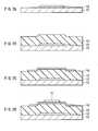
- FIGS. 2A to 2Dare diagrams illustrating a method of manufacturing the thin film transistor shown in FIGS. 1A and 1B in process order.
- FIG. 3is a diagram illustrating a circuit configuration of a display device using the thin film transistor shown in FIGS. 1A and 1B .
- FIG. 4is an equivalent circuit diagram illustrating an example of a pixel drive circuit shown in FIG. 3 .
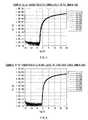
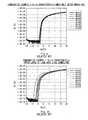
- FIG. 5is a diagram illustrating a Vg-Id characteristic immediately after annealing in the embodiment.
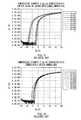
- FIG. 6is a diagram illustrating a Vg-Id characteristic after lapse of four days since the annealing in the embodiment.
- FIG. 7is a diagram illustrating a Vg-Id characteristic after lapse of seven days since the annealing in the embodiment.
- FIGS. 8A and 8Bare diagrams illustrating a stack-layer structure of a source electrode and a drain electrode of comparative examples 1 and 2.
- FIG. 9is a diagram illustrating a Vg-Id characteristic immediately after annealing in the comparative example 1.
- FIG. 10is a diagram illustrating a Vg-Id characteristic after lapse of four days since the annealing in the comparative example 1.
- FIG. 11is a diagram illustrating a Vg-Id characteristic after lapse of seven days since the annealing in the comparative example 1.
- FIG. 12is a diagram illustrating a Vg-Id characteristic immediately after annealing in the comparative example 2.
- FIG. 13is a diagram illustrating a Vg-Id characteristic after lapse of four days since the annealing in the comparative example 2.
- FIG. 14is a diagram illustrating a Vg-Id characteristic after lapse of seven days since the annealing in the comparative example 2.
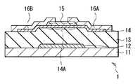
- FIG. 1Aillustrates a sectional structure of a thin film transistor 1 according to an embodiment of the present invention.
- FIG. 1Bis a diagram for explaining a layer structure of a source electrode 16 A and a drain electrode 16 B illustrated in FIG. 1A .
- the thin film transistor 1functions, for example, as a drive element for performing display driving of a liquid crystal display, an organic EL (Electro Luminescence) display, or the like and has, for example, a bottom-gate structure (inverted staggered structure).
- the thin film transistor 1has a gate electrode 12 in a selective region on a substrate 11 made of glass, plastic or the like, and a gate insulating film 13 is formed so as to cover the gate electrode 12 and the substrate 11 .
- An oxide semiconductor film 14is provided on the gate insulating film 13 , and a channel 14 A is formed in a region corresponding to the gate electrode 12 , in the oxide semiconductor film 14 .
- a channel protection film 15is provided immediately on the channel 14 A formed in the oxide semiconductor film 14 .
- the source electrode 16 A and the drain electrode 16 Bare disposed in a predetermined pattern so as to cover the oxide semiconductor film 14 exposed from the channel protection film 15 .
- the gate electrode 12is an electrode for applying gate voltage to the thin film transistor 1 .
- the gate electrode 12is made of, for example, molybdenum (Mo) or the like.
- the gate insulating film 13is constructed by a silicon oxide film, a silicon nitride film, a silicon nitride-oxide film, an aluminum oxide film, or the like.
- the oxide semiconductor film 14is constructed by using oxide semiconductor as a main component, and the channel 14 A for generating current between the source electrode 16 A and the drain electrode 16 B is formed.
- oxide semiconductorexamples include zinc oxide, In—M—Zn—O (M is at least one of gallium, aluminum, and iron), and the like.
- the channel protection film 15plays the role of preventing damage on the channel 14 A in the oxide semiconductor film 14 and preventing invasion of hydrogen or the like into the oxide semiconductor film 14 .
- the channel protection film 15also plays the role of protecting the channel 14 A from a resist peeling solution or the like used at the time of forming the source electrode 16 A and the drain electrode 16 B.
- Such a channel protection film 15is, for example, a silicon nitride film, a silicon oxide film, or the like.
- any of the source electrode 16 A and the drain electrode 16 Bis constructed by a multilayer film made of a plurality of metal layers.
- ithas a structure in which three layers of the first, second, and third metal layers 161 , 162 , and 163 are stacked.
- the first metal layer 161is formed along the interface with the oxide semiconductor film 14
- the second and third metal layers 162 and 163are formed in order on the first metal layer 161 .
- the first metal layer 161is made of, for example, a metal or alloy having ionization energy equal to or larger than that of molybdenum and has a thickness of, for example, 30 nm to 50 nm.
- the ionization energyis so-called first ionization energy, and the ionization energy of molybdenum is about 684 KJ/mol.
- An example of the metal of the first metal layer 161is molybdenum, mercury (Hg), silver (Ag), platinum (Pt), gold (Au), or the like.
- the first metal layer 161may be formed on the entire surface of the substrate 11 . However, it is sufficient to form the first metal layer 161 so as to cover at least the surface and side faces of the oxide semiconductor film 14 exposed from the channel protection film 15 .
- the second metal layer 162is made of a metal material having low electric resistance and excellent electrical conductivity, concretely, aluminum (Al), copper (Cu), or the like, and has a thickness of, for example, 300 nm to 1000 nm.
- the third metal layer 163is disposed to protect the surface of the second metal layer 162 , is made of titanium or the like, and has a thickness of, for example, 30 nm to 50 nm. In the source electrode 16 A and the drain electrode 16 B, the third metal layer 163 may not be formed. That is, a two-layer structure of the first and second metal layers 161 and 162 may be employed.
- the thin film transistor 1may be manufactured, for example, as follows. First, as shown in FIG. 2A , a metal thin film is formed on the entire surface of the substrate 11 by sputtering or vapor deposition. After that, the metal thin film is patterned by using, for example, photolithography to form the gate electrode 12 .
- the gate insulating film 13is formed so as to cover the substrate 11 and the gate electrode 12 by, for example, plasma CVD (Chemical Vapor Deposition).
- the oxide semiconductor film 14 made of the above-described material and having the above-described thicknessis formed by using, for example, sputtering.
- sputteringIn the case of using indium gallium zinc oxide (IGZO) as the oxide semiconductor, using DC sputtering targeting a ceramic of IGZO and plasma discharge using a mixture gas of argon (Ar) and oxygen (O 2 ), the oxide semiconductor film 14 is formed.
- a mixture gas of argon and oxygenis introduced before the plasma discharge is performed.
- the formed oxide semiconductor film 14is patterned by using, for example, photolithography.
- the channel protection film 15 made of the above-described materialis formed by, for example, sputtering. After that, by using, for example, photolithography, the channel protection film 15 is patterned so as to be formed in correspondence with the channel 14 A.
- the source electrode 16 A and the drain electrode 16 Bare formed on the oxide semiconductor film 14 .
- the first metal layer 161is formed by using, for example, sputtering so as to cover the region in which the oxide semiconductor film 14 and the channel protection film 15 are formed.
- the second and third metal layers 162 and 163are formed in order on the first metal layer 161 .
- the first, second, and third metal layers 161 , 162 , and 163are patterned by using, for example, photolithography, thereby forming the source electrode 16 A and the drain electrode 16 B.
- anneal processis performed on the substrate 11 on which the source electrode 16 A and the drain electrode 16 B in oxygen atmosphere.
- loss of oxygen in the oxide semiconductor film 14is prevented, and excellent electric characteristics are assured more easily.
- the thin film transistor 1 shown in FIG. 1Ais completed.
- the thin film transistor 1 of the embodimentwhen a voltage (gate voltage Vg) equal to or higher than the predetermined threshold voltage is applied to the gate electrode 12 via a not-shown wiring layer, the channel 14 A is formed in the oxide semiconductor film 14 , current (drain current Id) flows between the source electrode 16 A and the drain electrode 16 B, and the thin film transistor 1 functions as a transistor.
- the source electrode 16 A and the drain electrode 16 Bare formed on the oxide semiconductor film 14 in which the channel 14 A is formed.
- Each of the source electrode 16 A and the drain electrode 16 Bis obtained by stacking the first, second, and third metal layers 161 , 162 , and 163 from the side of the oxide semiconductor film 14 , and the first metal layer 161 is made of a metal having ionization energy equal to or higher than that of molybdenum. That is, the first metal layer 161 in contact with the oxide semiconductor film 14 is made of a metal which is not susceptible to oxidation.
- the metal layer in contact with the oxide semiconductor film 14is made of a metal having ionization energy smaller than that of molybdenum, that is, susceptible to oxidation
- oxygen in the oxide semiconductor film 14is taken to the side of the metal layer with oxidation of the metal layer. Consequently, the oxygen is desorbed to the outside of the oxide semiconductor film 14 . Due to loss of oxygen, carriers are generated in the oxide semiconductor layer 14 .
- the first metal layer 161 in contact with the oxide semiconductor film 14is made of a metal which is not susceptible to oxidation like in the embodiment, as compared with the case where the first metal layer 161 is made of a metal susceptible to oxidation, oxygen is not easily taken to the first metal layer 161 . Consequently, desorption of oxygen from the oxide semiconductor film 14 is suppressed, and generation of carries due to loss of oxygen is suppressed in the oxide semiconductor film 14 .
- the source electrode 16 A and the drain electrode 16 B in contact with the oxide semiconductor film 14has the stack-layer structure, and the first metal layer 161 in contact with the oxide semiconductor film 14 is made of a metal having ionization energy equal to or higher than that of molybdenum. Therefore, in the oxide semiconductor film 14 , generation of carriers due to loss of oxygen may be suppressed. It may suppress deterioration in the electric characteristics and improve reliability.
- the second metal layer 162is provided on the first metal layer 161 , and the second metal layer 162 is made of a metal having high conductivity.
- the first metal layer 161is made of molybdenum
- the formed oxide layerfunctions as an oxygen barrier layer, and exhaust of oxygen from the oxide semiconductor film 14 is suppressed. Therefore, in the case of making the first metal layer 161 of molybdenum, molybdenum itself is a metal which is not susceptible to oxidation and, in addition, by the oxygen barrier function of the oxide layer, loss of oxygen in the oxide semiconductor film 14 is effectively suppressed. Since the amount of oxygen taken to the side of the first metal layer 161 for oxidation of the surface is very small, the electric characteristics of the thin film transistor are sufficiently maintained.
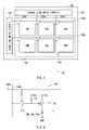
- FIG. 3illustrates a circuit configuration of a display device (display device 40 ) using the thin film transistor 1 as a drive device.
- the display device 40is, for example, a liquid crystal display or an organic EL display.
- a plurality of picture elements 10 R, 10 G, and 10 B disposed in a matrix and drive circuits for driving the picture elements 10 R, 10 G, and 10 Bare formed on a drive panel 50 .
- the picture elements 10 R, 10 G, and 10 Bare liquid crystal display elements, organic EL elements, or the like for emitting color light of red (R), green (G), and blue (B). Neighboring three picture elements 10 R, 10 G, and 10 B construct one pixel, and a display region 110 is formed by a plurality of pixels.
- a signal line drive circuit 120 and a scan line drive circuit 130 as drivers for video display, and a pixel drive circuit 140are disposed on the drive panel 50 .
- a not-shown sealing panelis adhered to the drive panel 50 . By the sealing panel, the picture elements 10 R, 10 G, and 10 B and the drive circuits are sealed.
- FIG. 4is an equivalent circuit diagram of the pixel drive circuit 140 .
- the pixel drive circuit 140is an active-type drive circuit in which transistors Tr 1 and Tr 2 are disposed as the thin film transistors 1 .
- a capacitor Csis provided between the transistors Tr 1 and Tr 2 , and the picture element 10 R (or the picture element 10 G or 10 B) is connected in series with the transistor Tr 1 between a first power supply line (Vcc) and a second power supply line (GND).
- Vccfirst power supply line
- GNDsecond power supply line
- a plurality of signal lines 120 Aare disposed in the column direction
- a plurality of scan lines 130 Aare disposed in the row direction.
- Each of the signal lines 120 Ais connected to the signal line drive circuit 120 , and an image signal is supplied from the signal line drive circuit 120 to the source electrode of the transistor Tr 2 via the signal line 120 A.
- Each of the scan lines 130 Ais connected to the scan line drive circuit 130 , and a scan signal is sequentially supplied from the scan line drive circuit 130 to the gate electrode of the transistor Tr 2 via the scan line 130 A.
- the thin film transistor 1 using molybdenum (50 nm thick) for the first metal layer 161 , aluminum (500 nm thick) for the second metal layer 162 , and titanium (50 nm thick) for the third metal layer 163was produced.
- Molybdenumwas used for the gate electrode 12
- silicon oxide (SiO) with film thickness 200 nmwas used for the gate insulating film 13
- In—Ga—Zn—Owas used for the oxide semiconductor film 14
- silicon oxide (SiO) with film thickness 200 nmwas used for the channel protection film 15 .
- oxygen concentration in an atmosphere including oxygen (O 2 ) and nitrogen (N 2 )was set to about 40%
- heat treatment temperaturewas set to 300° C.
- treatment timewas set to two hours.
- FIGS. 5 to 7illustrate the results of nine thin film transistors 1 (chip 1 to chip 9 ) produced under similar conditions.
- the metal layer which is in contact with the oxide semiconductor film 14is made of titanium in the comparative example 1 and is made of aluminum in the comparative example 2 (ionization energy of titanium>ionization energy of aluminum).
- the configuration other than the source electrode and the drain electrode having such a stack-layer structureis similar to that of the example.
- the Vg-Id characteristicdeteriorates with time from a time immediately after the annealing process to a time after lapse of seven days, and variations occurred among chips 1 to 9 .
- FIGS. 12 to 14in the comparative example 2 in which the aluminum layer 1062 is formed in contact with the oxide semiconductor film 14 , deterioration with time which is as large as that of the comparative example 1 is not seen in the Vg-Id characteristic, but variations occurred among chips 1 to 9 . Therefore, in the thin film transistors of the comparative examples 1 and 2, the electric characteristics tend to deteriorate at a stage before the thin film transistors are mounted on a panel of a display or the like.
- the Vg-Id characteristicis held almost constant for a period from a time immediately after the annealing process to a time after lapse of seven days, and fluctuations with time are extremely small.
- the Vg-Id characteristics of chips 1 to 9also hardly vary.
- the thin film transistor of the modificationis similar to the thin film transistor 1 of the foregoing embodiment except for the material of the metal layer (hereinbelow, simply called a first metal layer) which is in contact with the oxide semiconductor film 14 , in the stack-layer structure constructing the source electrode and the drain electrode. Consequently, the thin film transistor of the modification is not illustrated, the same reference numerals as those of the thin film transistor 1 of the embodiment are used for components, and repetitive description will not be given.
- the material of the metal layerhereinbelow, simply called a first metal layer
- the first metal layer of the modificationis made of a metal material having oxygen barrier property, concretely, a nitride or silicon nitride of any of the following metals.
- the metal used for the first metal layerinclude tantalum (Ta), vanadium (V), titanium (Ti), zirconium (Zr), tungsten (W), copper (Cu), aluminum (Al), ruthenium (Ru), iridium (Ir), nickel (Ni), cobalt (Co), and platinum (Pt).
- the first metal layer which is in contact with the oxide semiconductor film 14is not limited to a metal having predetermined ionization energy as described in the foregoing embodiment but may be made of a nitride or silicon nitride of a metal having oxygen barrier property.
- a metal having predetermined ionization energyas described in the foregoing embodiment but may be made of a nitride or silicon nitride of a metal having oxygen barrier property.
- the oxygen barrier function of the first metal layerby the oxygen barrier function of the first metal layer, desorption from the oxide semiconductor film 14 to the outside is suppressed. Therefore, generation of carriers due to loss of oxygen in the oxide semiconductor film 14 may be suppressed, and an effect similar to that of the foregoing embodiment may be obtained.
- the present inventionhas been described above by the embodiment and the modification, the invention is not limited to the foregoing embodiment and the like but may be variously modified.
- the source electrode and the drain electrodehave the stack-layer structure of the first, second, and third metal layers.
- the number of layersis not limited to three but may be two or four or more. Also in the case where the number of layers is two or four or more, if the metal layer which is in contact with the oxide semiconductor film is made of a metal having predetermined ionization energy or a metal having oxygen barrier property, an effect equivalent to that of the present invention may be obtained.
- the thin film transistor having the bottom gate structurehas been described as an example in the embodiment and the like, the invention is not limited to the bottom gate structure.
- a top gate structuremay be also employed.
Landscapes
- Thin Film Transistor (AREA)
- Liquid Crystal (AREA)
- Electrodes Of Semiconductors (AREA)
Abstract
Description
- 1. Field of the Invention
- The present invention relates to a thin film transistor using an oxide semiconductor film and a display device using the same.
- 2. Description of the Related Art
- In recent years, attention is being paid to a thin film transistor (TFT) using a semiconductor whose main component is an oxide (hereinbelow, called oxide semiconductor) for an active layer. It is known that the electron mobility of the oxide semiconductor is higher than that of amorphous silicon (α-Si) generally used for a liquid crystal display or the like, and the oxide semiconductor has excellent electric characteristics. As such oxide semiconductors, an oxide semiconductor whose main component is zinc oxide (ZnO) (refer to Patent document 1: Japanese Unexamined Patent Application Publication No. 2002-76356), an oxide semiconductor whose main component is In—M—Zn—O (M denotes at least one of gallium (Ga), aluminum (Al), and iron (Fe) (refer to Patent document 2: Japanese Unexamined Patent Application Publication No. 2007-134496), and the like are proposed. In a thin film transistor of the
patent document 2, by making a source electrode and a drain electrode formed on the oxide semiconductor, of a metal having a specific work function, a high on/off ratio is realized. - In such an oxide semiconductor, however, oxygen is desorbed with time in manufacture, operation, and the like and, due to this, a current-voltage characteristic of a thin film transistor deteriorates. It causes deterioration in reliability.
- It is therefore desirable to provide a thin film transistor realizing improved reliability by suppressing deterioration in electric characteristics and a display device using the same.
- According to an embodiment of the present invention, there is provided a thin film transistor including: an oxide semiconductor film forming a channel; a gate electrode disposed on one side of the oxide semiconductor film via a gate insulating film; and a pair of electrodes formed as a source electrode and a drain electrode in contact with the oxide semiconductor film and obtained by stacking each of first and second metal layers in order from the side of the oxide semiconductor film. The first metal layer is made of a metal having ionization energy equal to or higher than molybdenum (Mo), a metal having oxygen barrier property, or a nitride or a silicon nitride of the metal having oxygen barrier property.
- In the thin film transistor of the embodiment of the present invention, a pair of electrodes which are in contact with the oxide semiconductor film are obtained by stacking the first and second metal layers, and the first metal layer which is in contact with the oxide semiconductor film is made of a metal having ionization energy equal to or higher than that of molybdenum, that is, a metal which is not susceptible to oxidation. If the metal layer which is in contact with the oxide semiconductor film is made of a metal having ionization energy lower than that of molybdenum, that is, a metal which is susceptible to oxidation, oxygen in the oxide semiconductor film is easily taken to the side of the metal layer with oxidation of the metal layer. Consequently, if the metal susceptible to oxidation is in contact with the oxide semiconductor film, oxygen in the oxide semiconductor film is desorbed and loss occurs. Due to this, carriers are easily generated. Therefore, by making the first metal layer in contact with the oxide semiconductor film of a metal which is not susceptible to oxidation, generation of carriers due to loss of oxygen in the oxide semiconductor film is suppressed.
- Alternatively, by making the first metal layer of a metal having oxygen barrier property, or a nitride or a silicon nitride of the metal having oxygen barrier property, desorption of oxygen in the oxide semiconductor film to the outside may be suppressed. Therefore, like in the case where the first metal layer is made of a metal having predetermined ionization energy, generation of carriers in the oxide semiconductor film is suppressed.
- According to an embodiment of the present invention, there is provided a display device including a display element and the thin film transistor of an embodiment of the present invention.
- In the thin film transistor and the display device of the embodiment of the present invention, a pair of electrodes in contact with the oxide semiconductor film has a stack structure, and the first metal layer on the side of the oxide semiconductor film is made of a metal having ionization energy equal to or higher than that of molybdenum, a metal having oxygen barrier property, or a nitride or a silicon nitride of the metal having oxygen barrier property. Consequently, generation of carriers due to desorption of oxygen may be suppressed. Thus, deterioration in the electric characteristics is suppressed, and the reliability may be improved.
- Other and further objects, features and advantages of the invention will appear more fully from the following description.
FIGS. 1A and 1B express a sectional structure of a thin film transistor according to an embodiment of the present invention.FIGS. 2A to 2D are diagrams illustrating a method of manufacturing the thin film transistor shown inFIGS. 1A and 1B in process order.FIG. 3 is a diagram illustrating a circuit configuration of a display device using the thin film transistor shown inFIGS. 1A and 1B .FIG. 4 is an equivalent circuit diagram illustrating an example of a pixel drive circuit shown inFIG. 3 .FIG. 5 is a diagram illustrating a Vg-Id characteristic immediately after annealing in the embodiment.FIG. 6 is a diagram illustrating a Vg-Id characteristic after lapse of four days since the annealing in the embodiment.FIG. 7 is a diagram illustrating a Vg-Id characteristic after lapse of seven days since the annealing in the embodiment.FIGS. 8A and 8B are diagrams illustrating a stack-layer structure of a source electrode and a drain electrode of comparative examples 1 and 2.FIG. 9 is a diagram illustrating a Vg-Id characteristic immediately after annealing in the comparative example 1.FIG. 10 is a diagram illustrating a Vg-Id characteristic after lapse of four days since the annealing in the comparative example 1.FIG. 11 is a diagram illustrating a Vg-Id characteristic after lapse of seven days since the annealing in the comparative example 1.FIG. 12 is a diagram illustrating a Vg-Id characteristic immediately after annealing in the comparative example 2.FIG. 13 is a diagram illustrating a Vg-Id characteristic after lapse of four days since the annealing in the comparative example 2.FIG. 14 is a diagram illustrating a Vg-Id characteristic after lapse of seven days since the annealing in the comparative example 2.- Embodiments of the present invention will be described in detail hereinbelow with reference to the drawings.
FIG. 1A illustrates a sectional structure of athin film transistor 1 according to an embodiment of the present invention.FIG. 1B is a diagram for explaining a layer structure of asource electrode 16A and adrain electrode 16B illustrated inFIG. 1A . Thethin film transistor 1 functions, for example, as a drive element for performing display driving of a liquid crystal display, an organic EL (Electro Luminescence) display, or the like and has, for example, a bottom-gate structure (inverted staggered structure).- The
thin film transistor 1 has agate electrode 12 in a selective region on asubstrate 11 made of glass, plastic or the like, and agate insulating film 13 is formed so as to cover thegate electrode 12 and thesubstrate 11. Anoxide semiconductor film 14 is provided on thegate insulating film 13, and achannel 14A is formed in a region corresponding to thegate electrode 12, in theoxide semiconductor film 14. Achannel protection film 15 is provided immediately on thechannel 14A formed in theoxide semiconductor film 14. Thesource electrode 16A and thedrain electrode 16B are disposed in a predetermined pattern so as to cover theoxide semiconductor film 14 exposed from thechannel protection film 15. - The
gate electrode 12 is an electrode for applying gate voltage to thethin film transistor 1. Thegate electrode 12 is made of, for example, molybdenum (Mo) or the like. - The
gate insulating film 13 is constructed by a silicon oxide film, a silicon nitride film, a silicon nitride-oxide film, an aluminum oxide film, or the like. - The
oxide semiconductor film 14 is constructed by using oxide semiconductor as a main component, and thechannel 14A for generating current between thesource electrode 16A and thedrain electrode 16B is formed. Examples of the oxide semiconductor are zinc oxide, In—M—Zn—O (M is at least one of gallium, aluminum, and iron), and the like. - The
channel protection film 15 plays the role of preventing damage on thechannel 14A in theoxide semiconductor film 14 and preventing invasion of hydrogen or the like into theoxide semiconductor film 14. Thechannel protection film 15 also plays the role of protecting thechannel 14A from a resist peeling solution or the like used at the time of forming thesource electrode 16A and thedrain electrode 16B. Such achannel protection film 15 is, for example, a silicon nitride film, a silicon oxide film, or the like. - Any of the
source electrode 16A and thedrain electrode 16B is constructed by a multilayer film made of a plurality of metal layers. For example, as shown inFIG. 1B , it has a structure in which three layers of the first, second, andthird metal layers first metal layer 161 is formed along the interface with theoxide semiconductor film 14, and the second andthird metal layers first metal layer 161. - The
first metal layer 161 is made of, for example, a metal or alloy having ionization energy equal to or larger than that of molybdenum and has a thickness of, for example, 30 nm to 50 nm. The ionization energy is so-called first ionization energy, and the ionization energy of molybdenum is about 684 KJ/mol. An example of the metal of thefirst metal layer 161 is molybdenum, mercury (Hg), silver (Ag), platinum (Pt), gold (Au), or the like. Thefirst metal layer 161 may be formed on the entire surface of thesubstrate 11. However, it is sufficient to form thefirst metal layer 161 so as to cover at least the surface and side faces of theoxide semiconductor film 14 exposed from thechannel protection film 15. - The
second metal layer 162 is made of a metal material having low electric resistance and excellent electrical conductivity, concretely, aluminum (Al), copper (Cu), or the like, and has a thickness of, for example, 300 nm to 1000 nm. - The
third metal layer 163 is disposed to protect the surface of thesecond metal layer 162, is made of titanium or the like, and has a thickness of, for example, 30 nm to 50 nm. In thesource electrode 16A and thedrain electrode 16B, thethird metal layer 163 may not be formed. That is, a two-layer structure of the first andsecond metal layers - The
thin film transistor 1 may be manufactured, for example, as follows. First, as shown inFIG. 2A , a metal thin film is formed on the entire surface of thesubstrate 11 by sputtering or vapor deposition. After that, the metal thin film is patterned by using, for example, photolithography to form thegate electrode 12. - Subsequently, as shown in
FIG. 2B , thegate insulating film 13 is formed so as to cover thesubstrate 11 and thegate electrode 12 by, for example, plasma CVD (Chemical Vapor Deposition). - As shown in
FIG. 2C , theoxide semiconductor film 14 made of the above-described material and having the above-described thickness is formed by using, for example, sputtering. In the case of using indium gallium zinc oxide (IGZO) as the oxide semiconductor, using DC sputtering targeting a ceramic of IGZO and plasma discharge using a mixture gas of argon (Ar) and oxygen (O2), theoxide semiconductor film 14 is formed. Preferably, before the plasma discharge is performed, air is exhausted until the degree of vacuum in a vacuum vessel becomes, for example, 1×10⁻⁴Pa or less, and a mixture gas of argon and oxygen is introduced. After that, the formedoxide semiconductor film 14 is patterned by using, for example, photolithography. - Subsequently, as shown in
FIG. 2D , thechannel protection film 15 made of the above-described material is formed by, for example, sputtering. After that, by using, for example, photolithography, thechannel protection film 15 is patterned so as to be formed in correspondence with thechannel 14A. - Next, the
source electrode 16A and thedrain electrode 16B are formed on theoxide semiconductor film 14. At this time, thefirst metal layer 161 is formed by using, for example, sputtering so as to cover the region in which theoxide semiconductor film 14 and thechannel protection film 15 are formed. After that, the second andthird metal layers first metal layer 161. Subsequently, the first, second, andthird metal layers source electrode 16A and thedrain electrode 16B. - Finally, anneal process is performed on the
substrate 11 on which thesource electrode 16A and thedrain electrode 16B in oxygen atmosphere. By the process, loss of oxygen in theoxide semiconductor film 14 is prevented, and excellent electric characteristics are assured more easily. In such a manner, thethin film transistor 1 shown inFIG. 1A is completed. - In the
thin film transistor 1 of the embodiment, when a voltage (gate voltage Vg) equal to or higher than the predetermined threshold voltage is applied to thegate electrode 12 via a not-shown wiring layer, thechannel 14A is formed in theoxide semiconductor film 14, current (drain current Id) flows between thesource electrode 16A and thedrain electrode 16B, and thethin film transistor 1 functions as a transistor. - In the embodiment, on the
oxide semiconductor film 14 in which thechannel 14A is formed, thesource electrode 16A and thedrain electrode 16B are formed. Each of thesource electrode 16A and thedrain electrode 16B is obtained by stacking the first, second, andthird metal layers oxide semiconductor film 14, and thefirst metal layer 161 is made of a metal having ionization energy equal to or higher than that of molybdenum. That is, thefirst metal layer 161 in contact with theoxide semiconductor film 14 is made of a metal which is not susceptible to oxidation. - On the contrary, in the case where the metal layer in contact with the
oxide semiconductor film 14 is made of a metal having ionization energy smaller than that of molybdenum, that is, susceptible to oxidation, oxygen in theoxide semiconductor film 14 is taken to the side of the metal layer with oxidation of the metal layer. Consequently, the oxygen is desorbed to the outside of theoxide semiconductor film 14. Due to loss of oxygen, carriers are generated in theoxide semiconductor layer 14. - Therefore, since the
first metal layer 161 in contact with theoxide semiconductor film 14 is made of a metal which is not susceptible to oxidation like in the embodiment, as compared with the case where thefirst metal layer 161 is made of a metal susceptible to oxidation, oxygen is not easily taken to thefirst metal layer 161. Consequently, desorption of oxygen from theoxide semiconductor film 14 is suppressed, and generation of carries due to loss of oxygen is suppressed in theoxide semiconductor film 14. - As described above, in the
thin film transistor 1, thesource electrode 16A and thedrain electrode 16B in contact with theoxide semiconductor film 14 has the stack-layer structure, and thefirst metal layer 161 in contact with theoxide semiconductor film 14 is made of a metal having ionization energy equal to or higher than that of molybdenum. Therefore, in theoxide semiconductor film 14, generation of carriers due to loss of oxygen may be suppressed. It may suppress deterioration in the electric characteristics and improve reliability. - In the embodiment, in the
source electrode 16A and thedrain electrode 16B, thesecond metal layer 162 is provided on thefirst metal layer 161, and thesecond metal layer 162 is made of a metal having high conductivity. With the configuration, as compared with the case where thesource electrode 16A and thedrain electrode 16B are constructed by a single layer of thefirst metal layer 161, electric resistance may be reduced, and the functions of the source and drain and the wiring may be improved. - Particularly, in the case where the
first metal layer 161 is made of molybdenum, only the surface (the surface on theoxide semiconductor film 14 side) of thefirst metal layer 161 is oxidized, and an oxide layer is formed. In this case, the formed oxide layer functions as an oxygen barrier layer, and exhaust of oxygen from theoxide semiconductor film 14 is suppressed. Therefore, in the case of making thefirst metal layer 161 of molybdenum, molybdenum itself is a metal which is not susceptible to oxidation and, in addition, by the oxygen barrier function of the oxide layer, loss of oxygen in theoxide semiconductor film 14 is effectively suppressed. Since the amount of oxygen taken to the side of thefirst metal layer 161 for oxidation of the surface is very small, the electric characteristics of the thin film transistor are sufficiently maintained. FIG. 3 illustrates a circuit configuration of a display device (display device40) using thethin film transistor 1 as a drive device. Thedisplay device 40 is, for example, a liquid crystal display or an organic EL display. For example, on adrive panel 50, a plurality ofpicture elements picture elements picture elements picture elements display region 110 is formed by a plurality of pixels. As drive circuits, for example, a signalline drive circuit 120 and a scanline drive circuit 130 as drivers for video display, and apixel drive circuit 140 are disposed on thedrive panel 50. A not-shown sealing panel is adhered to thedrive panel 50. By the sealing panel, thepicture elements FIG. 4 is an equivalent circuit diagram of thepixel drive circuit 140. Thepixel drive circuit 140 is an active-type drive circuit in which transistors Tr1 and Tr2 are disposed as thethin film transistors 1. A capacitor Cs is provided between the transistors Tr1 and Tr2, and thepicture element 10R (or thepicture element pixel drive circuit 140, a plurality ofsignal lines 120A are disposed in the column direction, and a plurality ofscan lines 130A are disposed in the row direction. Each of thesignal lines 120A is connected to the signalline drive circuit 120, and an image signal is supplied from the signalline drive circuit 120 to the source electrode of the transistor Tr2 via thesignal line 120A. Each of thescan lines 130A is connected to the scanline drive circuit 130, and a scan signal is sequentially supplied from the scanline drive circuit 130 to the gate electrode of the transistor Tr2 via thescan line 130A.- As an example of the foregoing embodiment, the
thin film transistor 1 using molybdenum (50 nm thick) for thefirst metal layer 161, aluminum (500 nm thick) for thesecond metal layer 162, and titanium (50 nm thick) for thethird metal layer 163 was produced. Molybdenum was used for thegate electrode 12, silicon oxide (SiO) with film thickness 200 nm was used for thegate insulating film 13, In—Ga—Zn—O was used for theoxide semiconductor film 14, and silicon oxide (SiO) with film thickness 200 nm was used for thechannel protection film 15. As conditions of annealing process performed after formation of thesource electrode 16A and thedrain electrode 16B, oxygen concentration in an atmosphere including oxygen (O2) and nitrogen (N2) was set to about 40%, heat treatment temperature was set to 300° C., and treatment time was set to two hours. - To examine changes in the electric characteristics with time of such a
thin film transistor 1, changes in drain current Id (A) with respect to the gate voltage Vg (V) (hereinbelow, called Vg-Id characteristics) immediately after the annealing process, four days after the annealing process, and seven days after the annealing process were measured. The results were shown inFIGS. 5 to 7 .FIGS. 5 to 7 illustrate the results of nine thin film transistors1 (chip 1 to chip9) produced under similar conditions. - As comparative examples 1 and 2 of the example, thin film transistors each using a metal having ionization energy smaller than that of molybdenum for a metal layer which is in contact with the
oxide semiconductor film 14 as the source electrode and the drain electrode were produced. In the comparative example 1, as shown inFIG. 8A , a three-layer structure is employed in which a titanium layer1061 (50 nm thick), an aluminum layer1062 (500 nm thick), and a titanium layer1063 (50 nm thick) are stacked in order from the side of theoxide semiconductor film 14. On the other hand, in the comparative example 2, a two-layer structure is employed in which the aluminum layer1062 (500 nm thick) and the titanium layer1063 (50 nm thick) are stacked in order from the side of theoxide semiconductor film 14. That is, the metal layer which is in contact with theoxide semiconductor film 14 is made of titanium in the comparative example 1 and is made of aluminum in the comparative example 2 (ionization energy of titanium>ionization energy of aluminum). The configuration other than the source electrode and the drain electrode having such a stack-layer structure is similar to that of the example. - With respect to the thin film transistors of the comparative examples 1 and 2, in a manner similar to the example, changes in the drain current Id(A) relative to the gate voltage Vg (V) at some time points after the annealing process were measured. The result of the comparative example 1 is shown in
FIGS. 9 to 11 . The result of the comparative example 2 is shown inFIGS. 12 to 14 . - As shown in
FIGS. 9 to 11 , in the comparative example 1 in which thetitanium layer 1061 is formed in contact with theoxide semiconductor film 14, the Vg-Id characteristic deteriorates with time from a time immediately after the annealing process to a time after lapse of seven days, and variations occurred amongchips 1 to9. As shown inFIGS. 12 to 14 , in the comparative example 2 in which thealuminum layer 1062 is formed in contact with theoxide semiconductor film 14, deterioration with time which is as large as that of the comparative example 1 is not seen in the Vg-Id characteristic, but variations occurred amongchips 1 to9. Therefore, in the thin film transistors of the comparative examples 1 and 2, the electric characteristics tend to deteriorate at a stage before the thin film transistors are mounted on a panel of a display or the like. - In contrast, in the example in which the
first metal layer 161 in contact with theoxide semiconductor film 14 is made of molybdenum as shown inFIGS. 5 to 7 , the Vg-Id characteristic is held almost constant for a period from a time immediately after the annealing process to a time after lapse of seven days, and fluctuations with time are extremely small. The Vg-Id characteristics ofchips 1 to9 also hardly vary. - From the above results, it is known that by making the metal layer in contact with the
oxide semiconductor film 14 of a metal having ionization energy equal to or higher than that of molybdenum, that is, a metal which is not susceptible to oxidation, deterioration in the electric characteristic may be suppressed. - A thin film transistor according to a modification of the present invention will now be described. The thin film transistor of the modification is similar to the
thin film transistor 1 of the foregoing embodiment except for the material of the metal layer (hereinbelow, simply called a first metal layer) which is in contact with theoxide semiconductor film 14, in the stack-layer structure constructing the source electrode and the drain electrode. Consequently, the thin film transistor of the modification is not illustrated, the same reference numerals as those of thethin film transistor 1 of the embodiment are used for components, and repetitive description will not be given. - The first metal layer of the modification is made of a metal material having oxygen barrier property, concretely, a nitride or silicon nitride of any of the following metals. Examples of the metal used for the first metal layer include tantalum (Ta), vanadium (V), titanium (Ti), zirconium (Zr), tungsten (W), copper (Cu), aluminum (Al), ruthenium (Ru), iridium (Ir), nickel (Ni), cobalt (Co), and platinum (Pt).
- The first metal layer which is in contact with the
oxide semiconductor film 14 is not limited to a metal having predetermined ionization energy as described in the foregoing embodiment but may be made of a nitride or silicon nitride of a metal having oxygen barrier property. In this case, by the oxygen barrier function of the first metal layer, desorption from theoxide semiconductor film 14 to the outside is suppressed. Therefore, generation of carriers due to loss of oxygen in theoxide semiconductor film 14 may be suppressed, and an effect similar to that of the foregoing embodiment may be obtained. - Although the present invention has been described above by the embodiment and the modification, the invention is not limited to the foregoing embodiment and the like but may be variously modified. For example, in the embodiment and the like, the source electrode and the drain electrode have the stack-layer structure of the first, second, and third metal layers. The number of layers is not limited to three but may be two or four or more. Also in the case where the number of layers is two or four or more, if the metal layer which is in contact with the oxide semiconductor film is made of a metal having predetermined ionization energy or a metal having oxygen barrier property, an effect equivalent to that of the present invention may be obtained.
- Although the thin film transistor having the bottom gate structure has been described as an example in the embodiment and the like, the invention is not limited to the bottom gate structure. A top gate structure may be also employed.
- The present application contains subject matter related to that disclosed in Japanese Priority Patent Application JP 2008-293043 filed in the Japan Patent Office on Nov. 17, 2008, the entire content of which is hereby incorporated by reference.
- It should be understood by those skilled in the art that various modifications, combinations, sub-combinations and alterations may occur depending on design requirements and other factors insofar as they are within the scope of the appended claims or the equivalents thereof.
Claims (6)
Priority Applications (1)
| Application Number | Priority Date | Filing Date | Title |
|---|---|---|---|
| US13/533,328US20120267625A1 (en) | 2008-11-17 | 2012-06-26 | Thin film transistor and display device |
Applications Claiming Priority (2)
| Application Number | Priority Date | Filing Date | Title |
|---|---|---|---|
| JP2008-293043 | 2008-11-17 | ||
| JP2008293043AJP2010123595A (en) | 2008-11-17 | 2008-11-17 | Thin film transistor and display |
Related Child Applications (1)
| Application Number | Title | Priority Date | Filing Date |
|---|---|---|---|
| US13/533,328ContinuationUS20120267625A1 (en) | 2008-11-17 | 2012-06-26 | Thin film transistor and display device |
Publications (2)
| Publication Number | Publication Date |
|---|---|
| US20100123131A1true US20100123131A1 (en) | 2010-05-20 |
| US8319226B2 US8319226B2 (en) | 2012-11-27 |
Family
ID=42171262
Family Applications (2)
| Application Number | Title | Priority Date | Filing Date |
|---|---|---|---|
| US12/619,299Active2030-04-22US8319226B2 (en) | 2008-11-17 | 2009-11-16 | Thin film transistor and display device |
| US13/533,328AbandonedUS20120267625A1 (en) | 2008-11-17 | 2012-06-26 | Thin film transistor and display device |
Family Applications After (1)
| Application Number | Title | Priority Date | Filing Date |
|---|---|---|---|
| US13/533,328AbandonedUS20120267625A1 (en) | 2008-11-17 | 2012-06-26 | Thin film transistor and display device |
Country Status (3)
| Country | Link |
|---|---|
| US (2) | US8319226B2 (en) |
| JP (1) | JP2010123595A (en) |
| CN (1) | CN101740636B (en) |
Cited By (19)
| Publication number | Priority date | Publication date | Assignee | Title |
|---|---|---|---|---|
| US20120211755A1 (en)* | 2011-02-17 | 2012-08-23 | Sony Corporation | Thin film transistor, manufacturing method of thin film transistor and display |
| US20140008651A1 (en)* | 2008-12-02 | 2014-01-09 | Arizona Board of Regents, a body corporate of the State of Arizona Acting for and on behalf of Arizo | Dual active layers for semiconductor devices and methods of manufacturing the same |
| US20140061633A1 (en)* | 2012-01-13 | 2014-03-06 | Chengdu Boe Optoelectronics Technology Co., Ltd. | Oxide tft and manufacturing method thereof |
| US20150008429A1 (en)* | 2012-01-23 | 2015-01-08 | Sharp Kabushiki Kaisha | Method of manufacturing thin film transistor substrate and thin film transistor substrate manufactured by the method |
| US9099438B2 (en) | 2012-05-11 | 2015-08-04 | Samsung Display Co., Ltd. | Thin film transistor array panel |
| US9293478B2 (en) | 2012-10-31 | 2016-03-22 | Lg Display Co., Ltd. | Method of fabricating array substrate |
| US20160190327A1 (en)* | 2014-12-25 | 2016-06-30 | Hon Hai Precision Industry Co., Ltd. | Thin film transistor substrate, manufacturing method thereof, and liquid crystal display panel using same |
| US20160204232A1 (en)* | 2011-01-12 | 2016-07-14 | Semiconductor Energy Laboratory Co., Ltd. | Manufacturing method of the semiconductor device |
| US9502235B2 (en) | 2012-02-27 | 2016-11-22 | Boe Technology Group Co., Ltd. | Thin film transistor, method for manufacturing the same, array substrate and display device |
| US9601530B2 (en) | 2008-12-02 | 2017-03-21 | Arizona Board Of Regents, A Body Corporated Of The State Of Arizona, Acting For And On Behalf Of Arizona State University | Dual active layer semiconductor device and method of manufacturing the same |
| US9721825B2 (en) | 2008-12-02 | 2017-08-01 | Arizona Board Of Regents, A Body Corporate Of The State Of Arizona, Acting For And On Behalf Of Arizona State University | Method of providing a flexible semiconductor device and flexible semiconductor device thereof |
| US9741742B2 (en) | 2014-12-22 | 2017-08-22 | Arizona Board Of Regents, A Body Corporate Of The State Of Arizona, Acting For And On Behalf Of Arizona State University | Deformable electronic device and methods of providing and using deformable electronic device |
| US9768107B2 (en) | 2014-01-23 | 2017-09-19 | Arizona Board Of Regents, A Body Corporate Of The State Of Arizona, Acting For And On Behalf Of Arizona State University | Method of providing a flexible semiconductor device and flexible semiconductor device thereof |
| US9852904B2 (en)* | 2012-10-17 | 2017-12-26 | Semiconductor Energy Laboratory Co., Ltd. | Method for manufacturing semiconductor device |
| US9953951B2 (en) | 2014-05-13 | 2018-04-24 | Arizona Board Of Regents On Behalf Of Arizona State University | Method of providing a flexible semiconductor device and flexible semiconductor device thereof |
| US9991311B2 (en) | 2008-12-02 | 2018-06-05 | Arizona Board Of Regents On Behalf Of Arizona State University | Dual active layer semiconductor device and method of manufacturing the same |
| US10381224B2 (en) | 2014-01-23 | 2019-08-13 | Arizona Board Of Regents On Behalf Of Arizona State University | Method of providing an electronic device and electronic device thereof |
| US10410903B2 (en) | 2014-01-23 | 2019-09-10 | Arizona Board Of Regents On Behalf Of Arizona State University | Method of providing an electronic device and electronic device thereof |
| US10446582B2 (en) | 2014-12-22 | 2019-10-15 | Arizona Board Of Regents On Behalf Of Arizona State University | Method of providing an imaging system and imaging system thereof |
Families Citing this family (6)
| Publication number | Priority date | Publication date | Assignee | Title |
|---|---|---|---|---|
| KR102241766B1 (en) | 2009-12-04 | 2021-04-19 | 가부시키가이샤 한도오따이 에네루기 켄큐쇼 | Semiconductor device and manufacturing method thereof |
| KR101797253B1 (en) | 2009-12-04 | 2017-11-13 | 가부시키가이샤 한도오따이 에네루기 켄큐쇼 | Semiconductor device and manufacturing method thereof |
| TWI621184B (en)* | 2010-08-16 | 2018-04-11 | 半導體能源研究所股份有限公司 | Semiconductor device manufacturing method |
| JP2012119664A (en)* | 2010-11-12 | 2012-06-21 | Kobe Steel Ltd | Wiring structure |
| CN103137701B (en)* | 2011-11-30 | 2018-01-19 | 株式会社半导体能源研究所 | Transistor and semiconductor device |
| JP2015158572A (en)* | 2014-02-24 | 2015-09-03 | 株式会社Joled | Display device, electronic apparatus |
Citations (4)
| Publication number | Priority date | Publication date | Assignee | Title |
|---|---|---|---|---|
| US20020135709A1 (en)* | 2001-03-21 | 2002-09-26 | Gee Sung Chae | Liquid crystal display device and fabricating method thereof |
| US20050122443A1 (en)* | 2003-12-04 | 2005-06-09 | Lg.Philips Lcd Co., Ltd. | Array substrate for liquid crystal display device and fabricating method thereof |
| US20070072439A1 (en)* | 2005-09-29 | 2007-03-29 | Semiconductor Energy Laboratory Co., Ltd. | Semiconductor device and manufacturing method thereof |
| US20080315200A1 (en)* | 2007-06-19 | 2008-12-25 | Samsung Electronics Co., Ltd. | Oxide semiconductors and thin film transistors comprising the same |
Family Cites Families (15)
| Publication number | Priority date | Publication date | Assignee | Title |
|---|---|---|---|---|
| JP2000002892A (en)* | 1998-04-17 | 2000-01-07 | Toshiba Corp | Liquid crystal display device, matrix array substrate and method of manufacturing the same |
| JP4089858B2 (en) | 2000-09-01 | 2008-05-28 | 国立大学法人東北大学 | Semiconductor device |
| US20030122987A1 (en)* | 2001-12-28 | 2003-07-03 | Myung-Joon Kim | Array substrate for a liquid crystal display device having multi-layered metal line and fabricating method thereof |
| JP3672256B2 (en)* | 2002-08-08 | 2005-07-20 | インターナショナル・ビジネス・マシーンズ・コーポレーション | Etching solution, thin film transistor array substrate, method for manufacturing thin film transistor array substrate, and display device |
| JP4299717B2 (en)* | 2004-04-14 | 2009-07-22 | Nec液晶テクノロジー株式会社 | Thin film transistor and manufacturing method thereof |
| KR101107246B1 (en) | 2004-12-24 | 2012-01-25 | 엘지디스플레이 주식회사 | Thin film transistor substrate and its manufacturing method |
| US7411298B2 (en)* | 2005-08-17 | 2008-08-12 | Kabushiki Kaisha Kobe Seiko Sho (Kobe Steel, Ltd.) | Source/drain electrodes, thin-film transistor substrates, manufacture methods thereof, and display devices |
| JP5064747B2 (en)* | 2005-09-29 | 2012-10-31 | 株式会社半導体エネルギー研究所 | Semiconductor device, electrophoretic display device, display module, electronic device, and method for manufacturing semiconductor device |
| JP4793679B2 (en) | 2005-11-10 | 2011-10-12 | 富士電機株式会社 | Thin film transistor |
| KR101206033B1 (en)* | 2006-04-18 | 2012-11-28 | 삼성전자주식회사 | Fabrication method of ZnO Thin Film and ZnO Transistor, and Thin Film Transistor adopting the same |
| TWI320233B (en)* | 2006-09-12 | 2010-02-01 | Pixel structure and fabricating method thereof | |
| KR20080037296A (en)* | 2006-10-25 | 2008-04-30 | 삼성전자주식회사 | Thin film transistor substrate and manufacturing method thereof |
| JP5305630B2 (en)* | 2006-12-05 | 2013-10-02 | キヤノン株式会社 | Manufacturing method of bottom gate type thin film transistor and manufacturing method of display device |
| JP2008235871A (en)* | 2007-02-20 | 2008-10-02 | Canon Inc | Thin film transistor forming method and display device |
| JP5213422B2 (en) | 2007-12-04 | 2013-06-19 | キヤノン株式会社 | Oxide semiconductor element having insulating layer and display device using the same |
- 2008
- 2008-11-17JPJP2008293043Apatent/JP2010123595A/enactivePending
- 2009
- 2009-11-16USUS12/619,299patent/US8319226B2/enactiveActive
- 2009-11-17CNCN2009102245271Apatent/CN101740636B/enactiveActive
- 2012
- 2012-06-26USUS13/533,328patent/US20120267625A1/ennot_activeAbandoned
Patent Citations (4)
| Publication number | Priority date | Publication date | Assignee | Title |
|---|---|---|---|---|
| US20020135709A1 (en)* | 2001-03-21 | 2002-09-26 | Gee Sung Chae | Liquid crystal display device and fabricating method thereof |
| US20050122443A1 (en)* | 2003-12-04 | 2005-06-09 | Lg.Philips Lcd Co., Ltd. | Array substrate for liquid crystal display device and fabricating method thereof |
| US20070072439A1 (en)* | 2005-09-29 | 2007-03-29 | Semiconductor Energy Laboratory Co., Ltd. | Semiconductor device and manufacturing method thereof |
| US20080315200A1 (en)* | 2007-06-19 | 2008-12-25 | Samsung Electronics Co., Ltd. | Oxide semiconductors and thin film transistors comprising the same |
Cited By (28)
| Publication number | Priority date | Publication date | Assignee | Title |
|---|---|---|---|---|
| US9991311B2 (en) | 2008-12-02 | 2018-06-05 | Arizona Board Of Regents On Behalf Of Arizona State University | Dual active layer semiconductor device and method of manufacturing the same |
| US9601530B2 (en) | 2008-12-02 | 2017-03-21 | Arizona Board Of Regents, A Body Corporated Of The State Of Arizona, Acting For And On Behalf Of Arizona State University | Dual active layer semiconductor device and method of manufacturing the same |
| US9721825B2 (en) | 2008-12-02 | 2017-08-01 | Arizona Board Of Regents, A Body Corporate Of The State Of Arizona, Acting For And On Behalf Of Arizona State University | Method of providing a flexible semiconductor device and flexible semiconductor device thereof |
| US20140008651A1 (en)* | 2008-12-02 | 2014-01-09 | Arizona Board of Regents, a body corporate of the State of Arizona Acting for and on behalf of Arizo | Dual active layers for semiconductor devices and methods of manufacturing the same |
| US9818850B2 (en)* | 2011-01-12 | 2017-11-14 | Semiconductor Energy Laboratory Co., Ltd. | Manufacturing method of the semiconductor device |
| US10593786B2 (en) | 2011-01-12 | 2020-03-17 | Semiconductor Energy Laboratory Co., Ltd. | Manufacturing method of the semiconductor device |
| US20160204232A1 (en)* | 2011-01-12 | 2016-07-14 | Semiconductor Energy Laboratory Co., Ltd. | Manufacturing method of the semiconductor device |
| US20120211755A1 (en)* | 2011-02-17 | 2012-08-23 | Sony Corporation | Thin film transistor, manufacturing method of thin film transistor and display |
| US20140061633A1 (en)* | 2012-01-13 | 2014-03-06 | Chengdu Boe Optoelectronics Technology Co., Ltd. | Oxide tft and manufacturing method thereof |
| US9355838B2 (en)* | 2012-01-13 | 2016-05-31 | Boe Technology Group Co., Ltd. | Oxide TFT and manufacturing method thereof |
| US20150008429A1 (en)* | 2012-01-23 | 2015-01-08 | Sharp Kabushiki Kaisha | Method of manufacturing thin film transistor substrate and thin film transistor substrate manufactured by the method |
| US9209282B2 (en)* | 2012-01-23 | 2015-12-08 | Sharp Kabushiki Kaisha | Method of manufacturing thin film transistor substrate and thin film transistor substrate manufactured by the method |
| US9502235B2 (en) | 2012-02-27 | 2016-11-22 | Boe Technology Group Co., Ltd. | Thin film transistor, method for manufacturing the same, array substrate and display device |
| US9245906B2 (en) | 2012-05-11 | 2016-01-26 | Samsung Display Co., Ltd. | Thin film transistor array panel |
| US9099438B2 (en) | 2012-05-11 | 2015-08-04 | Samsung Display Co., Ltd. | Thin film transistor array panel |
| US9852904B2 (en)* | 2012-10-17 | 2017-12-26 | Semiconductor Energy Laboratory Co., Ltd. | Method for manufacturing semiconductor device |
| US9293478B2 (en) | 2012-10-31 | 2016-03-22 | Lg Display Co., Ltd. | Method of fabricating array substrate |
| US9640567B2 (en) | 2012-10-31 | 2017-05-02 | Lg Display Co., Ltd. | Method of fabricating array substrate |
| US10043679B2 (en) | 2012-10-31 | 2018-08-07 | Lg Display Co., Ltd. | Method of fabricating array substrate |
| US10410903B2 (en) | 2014-01-23 | 2019-09-10 | Arizona Board Of Regents On Behalf Of Arizona State University | Method of providing an electronic device and electronic device thereof |
| US9768107B2 (en) | 2014-01-23 | 2017-09-19 | Arizona Board Of Regents, A Body Corporate Of The State Of Arizona, Acting For And On Behalf Of Arizona State University | Method of providing a flexible semiconductor device and flexible semiconductor device thereof |
| US10381224B2 (en) | 2014-01-23 | 2019-08-13 | Arizona Board Of Regents On Behalf Of Arizona State University | Method of providing an electronic device and electronic device thereof |
| US9953951B2 (en) | 2014-05-13 | 2018-04-24 | Arizona Board Of Regents On Behalf Of Arizona State University | Method of providing a flexible semiconductor device and flexible semiconductor device thereof |
| US10170407B2 (en) | 2014-12-22 | 2019-01-01 | Arizona Board Of Regents On Behalf Of Arizona State University | Electronic device and methods of providing and using electronic device |
| US9741742B2 (en) | 2014-12-22 | 2017-08-22 | Arizona Board Of Regents, A Body Corporate Of The State Of Arizona, Acting For And On Behalf Of Arizona State University | Deformable electronic device and methods of providing and using deformable electronic device |
| US10446582B2 (en) | 2014-12-22 | 2019-10-15 | Arizona Board Of Regents On Behalf Of Arizona State University | Method of providing an imaging system and imaging system thereof |
| US9893197B2 (en)* | 2014-12-25 | 2018-02-13 | Hon Hai Precision Industry Co., Ltd. | Thin film transistor substrate, manufacturing method thereof, and liquid crystal display panel using same |
| US20160190327A1 (en)* | 2014-12-25 | 2016-06-30 | Hon Hai Precision Industry Co., Ltd. | Thin film transistor substrate, manufacturing method thereof, and liquid crystal display panel using same |
Also Published As
| Publication number | Publication date |
|---|---|
| JP2010123595A (en) | 2010-06-03 |
| US20120267625A1 (en) | 2012-10-25 |
| CN101740636A (en) | 2010-06-16 |
| CN101740636B (en) | 2013-06-19 |
| US8319226B2 (en) | 2012-11-27 |
Similar Documents
| Publication | Publication Date | Title |
|---|---|---|
| US8319226B2 (en) | Thin film transistor and display device | |
| JP4752925B2 (en) | Thin film transistor and display device | |
| KR101738379B1 (en) | Semiconductor device | |
| JP5668917B2 (en) | Thin film transistor and manufacturing method thereof | |
| US9178072B2 (en) | Thin film transistor and display device | |
| JP5552753B2 (en) | Thin film transistor and display device | |
| KR101835748B1 (en) | Light-emitting display device and electronic device including the same | |
| US20120211755A1 (en) | Thin film transistor, manufacturing method of thin film transistor and display | |
| JP2011222767A (en) | Thin film transistor, display device, and electronic device | |
| CN102157558A (en) | Thin film transistor, method of manufacturing the same, and display unit | |
| US20160336386A1 (en) | Thin-film transistor substrate and method of manufacturing the thin-film transistor substrate | |
| CN102683383A (en) | Display device and electronic device | |
| KR20150100295A (en) | Preparing method for organic light emitting display device | |
| JPWO2014196107A1 (en) | THIN FILM TRANSISTOR ELEMENT, ITS MANUFACTURING METHOD, AND DISPLAY DEVICE | |
| US8981368B2 (en) | Thin film transistor, method of manufacturing thin film transistor, display, and electronic apparatus | |
| JP5527225B2 (en) | Thin film transistor and display device | |
| JP6260992B2 (en) | Thin film transistor and manufacturing method thereof | |
| JP6019330B2 (en) | THIN FILM TRANSISTOR, METHOD FOR PRODUCING THIN FILM TRANSISTOR, DISPLAY DEVICE, AND ELECTRONIC DEVICE |
Legal Events
| Date | Code | Title | Description |
|---|---|---|---|
| AS | Assignment | Owner name:SONY CORPORATION,JAPAN Free format text:ASSIGNMENT OF ASSIGNORS INTEREST;ASSIGNOR:TOKUNAGA, KAZUHIKO;REEL/FRAME:023523/0411 Effective date:20091105 Owner name:SONY CORPORATION, JAPAN Free format text:ASSIGNMENT OF ASSIGNORS INTEREST;ASSIGNOR:TOKUNAGA, KAZUHIKO;REEL/FRAME:023523/0411 Effective date:20091105 | |
| STCF | Information on status: patent grant | Free format text:PATENTED CASE | |
| FEPP | Fee payment procedure | Free format text:PAYOR NUMBER ASSIGNED (ORIGINAL EVENT CODE: ASPN); ENTITY STATUS OF PATENT OWNER: LARGE ENTITY | |
| AS | Assignment | Owner name:JOLED INC., JAPAN Free format text:ASSIGNMENT OF ASSIGNORS INTEREST;ASSIGNOR:SONY CORPORATION;REEL/FRAME:036106/0355 Effective date:20150618 | |
| FPAY | Fee payment | Year of fee payment:4 | |
| MAFP | Maintenance fee payment | Free format text:PAYMENT OF MAINTENANCE FEE, 8TH YEAR, LARGE ENTITY (ORIGINAL EVENT CODE: M1552); ENTITY STATUS OF PATENT OWNER: LARGE ENTITY Year of fee payment:8 | |
| AS | Assignment | Owner name:INCJ, LTD., JAPAN Free format text:SECURITY INTEREST;ASSIGNOR:JOLED, INC.;REEL/FRAME:063396/0671 Effective date:20230112 | |
| AS | Assignment | Owner name:JOLED, INC., JAPAN Free format text:CORRECTION BY AFFIDAVIT FILED AGAINST REEL/FRAME 063396/0671;ASSIGNOR:JOLED, INC.;REEL/FRAME:064067/0723 Effective date:20230425 | |
| AS | Assignment | Owner name:JDI DESIGN AND DEVELOPMENT G.K., JAPAN Free format text:ASSIGNMENT OF ASSIGNORS INTEREST;ASSIGNOR:JOLED, INC.;REEL/FRAME:066382/0619 Effective date:20230714 | |
| MAFP | Maintenance fee payment | Free format text:PAYMENT OF MAINTENANCE FEE, 12TH YEAR, LARGE ENTITY (ORIGINAL EVENT CODE: M1553); ENTITY STATUS OF PATENT OWNER: LARGE ENTITY Year of fee payment:12 | |
| AS | Assignment | Owner name:MAGNOLIA BLUE CORPORATION, JAPAN Free format text:ASSIGNMENT OF ASSIGNORS INTEREST;ASSIGNOR:JDI DESIGN AND DEVELOPMENT G.K.;REEL/FRAME:072039/0656 Effective date:20250625 |