US20100112818A1 - Method for forming high density patterns - Google Patents
Method for forming high density patternsDownload PDFInfo
- Publication number
- US20100112818A1 US20100112818A1US12/686,602US68660210AUS2010112818A1US 20100112818 A1US20100112818 A1US 20100112818A1US 68660210 AUS68660210 AUS 68660210AUS 2010112818 A1US2010112818 A1US 2010112818A1
- Authority
- US
- United States
- Prior art keywords
- holes
- pattern
- pillars
- features
- density
- Prior art date
- Legal status (The legal status is an assumption and is not a legal conclusion. Google has not performed a legal analysis and makes no representation as to the accuracy of the status listed.)
- Granted
Links
- 238000000034methodMethods0.000titleclaimsabstractdescription69
- 239000000758substrateSubstances0.000claimsabstractdescription33
- 238000005530etchingMethods0.000claimsabstractdescription22
- 239000000463materialSubstances0.000claimsdescription65
- 125000006850spacer groupChemical group0.000claimsdescription53
- 238000000151depositionMethods0.000claimsdescription22
- 230000008021depositionEffects0.000abstractdescription7
- 229920002120photoresistant polymerPolymers0.000description16
- 238000000206photolithographyMethods0.000description10
- 229910003481amorphous carbonInorganic materials0.000description5
- 238000005229chemical vapour depositionMethods0.000description5
- 238000009966trimmingMethods0.000description5
- 239000006117anti-reflective coatingSubstances0.000description4
- 230000000873masking effectEffects0.000description4
- 238000000623plasma-assisted chemical vapour depositionMethods0.000description3
- 239000004065semiconductorSubstances0.000description3
- 102100022717Atypical chemokine receptor 1Human genes0.000description2
- 101000678879Homo sapiens Atypical chemokine receptor 1Proteins0.000description2
- VYPSYNLAJGMNEJ-UHFFFAOYSA-NSilicium dioxideChemical compoundO=[Si]=OVYPSYNLAJGMNEJ-UHFFFAOYSA-N0.000description2
- 238000005137deposition processMethods0.000description2
- -1i.e.Polymers0.000description2
- 238000003384imaging methodMethods0.000description2
- 229910052814silicon oxideInorganic materials0.000description2
- 238000004528spin coatingMethods0.000description2
- OKTJSMMVPCPJKN-UHFFFAOYSA-NCarbonChemical compound[C]OKTJSMMVPCPJKN-UHFFFAOYSA-N0.000description1
- 229910052581Si3N4Inorganic materials0.000description1
- XUIMIQQOPSSXEZ-UHFFFAOYSA-NSiliconChemical compound[Si]XUIMIQQOPSSXEZ-UHFFFAOYSA-N0.000description1
- ATJFFYVFTNAWJD-UHFFFAOYSA-NTinChemical compound[Sn]ATJFFYVFTNAWJD-UHFFFAOYSA-N0.000description1
- VZPPHXVFMVZRTE-UHFFFAOYSA-N[Kr]FChemical compound[Kr]FVZPPHXVFMVZRTE-UHFFFAOYSA-N0.000description1
- 238000007792additionMethods0.000description1
- PNEYBMLMFCGWSK-UHFFFAOYSA-Naluminium oxideInorganic materials[O-2].[O-2].[O-2].[Al+3].[Al+3]PNEYBMLMFCGWSK-UHFFFAOYSA-N0.000description1
- ISQINHMJILFLAQ-UHFFFAOYSA-Nargon hydrofluorideChemical compoundF.[Ar]ISQINHMJILFLAQ-UHFFFAOYSA-N0.000description1
- 238000000231atomic layer depositionMethods0.000description1
- 229910052799carbonInorganic materials0.000description1
- 229910052593corundumInorganic materials0.000description1
- 238000010894electron beam technologyMethods0.000description1
- 238000007654immersionMethods0.000description1
- 239000011810insulating materialSubstances0.000description1
- 238000001459lithographyMethods0.000description1
- 238000004519manufacturing processMethods0.000description1
- 238000012986modificationMethods0.000description1
- 230000004048modificationEffects0.000description1
- 238000001127nanoimprint lithographyMethods0.000description1
- 238000007517polishing processMethods0.000description1
- 229910021420polycrystalline siliconInorganic materials0.000description1
- 229920005591polysiliconPolymers0.000description1
- 239000002243precursorSubstances0.000description1
- 230000001681protective effectEffects0.000description1
- 238000000926separation methodMethods0.000description1
- 229910052710siliconInorganic materials0.000description1
- 239000010703siliconSubstances0.000description1
- HQVNEWCFYHHQES-UHFFFAOYSA-Nsilicon nitrideChemical compoundN12[Si]34N5[Si]62N3[Si]51N64HQVNEWCFYHHQES-UHFFFAOYSA-N0.000description1
- 239000007787solidSubstances0.000description1
- 239000000126substanceSubstances0.000description1
- 229910052718tinInorganic materials0.000description1
- 229910001845yogo sapphireInorganic materials0.000description1
Images


Classifications
- H—ELECTRICITY
- H01—ELECTRIC ELEMENTS
- H01L—SEMICONDUCTOR DEVICES NOT COVERED BY CLASS H10
- H01L21/00—Processes or apparatus adapted for the manufacture or treatment of semiconductor or solid state devices or of parts thereof
- H01L21/70—Manufacture or treatment of devices consisting of a plurality of solid state components formed in or on a common substrate or of parts thereof; Manufacture of integrated circuit devices or of parts thereof
- H01L21/71—Manufacture of specific parts of devices defined in group H01L21/70
- H01L21/768—Applying interconnections to be used for carrying current between separate components within a device comprising conductors and dielectrics
- H01L21/76838—Applying interconnections to be used for carrying current between separate components within a device comprising conductors and dielectrics characterised by the formation and the after-treatment of the conductors
- H01L21/76885—By forming conductive members before deposition of protective insulating material, e.g. pillars, studs
- H—ELECTRICITY
- H01—ELECTRIC ELEMENTS
- H01L—SEMICONDUCTOR DEVICES NOT COVERED BY CLASS H10
- H01L21/00—Processes or apparatus adapted for the manufacture or treatment of semiconductor or solid state devices or of parts thereof
- H01L21/02—Manufacture or treatment of semiconductor devices or of parts thereof
- H01L21/027—Making masks on semiconductor bodies for further photolithographic processing not provided for in group H01L21/18 or H01L21/34
- H01L21/033—Making masks on semiconductor bodies for further photolithographic processing not provided for in group H01L21/18 or H01L21/34 comprising inorganic layers
- H01L21/0334—Making masks on semiconductor bodies for further photolithographic processing not provided for in group H01L21/18 or H01L21/34 comprising inorganic layers characterised by their size, orientation, disposition, behaviour, shape, in horizontal or vertical plane
- H01L21/0337—Making masks on semiconductor bodies for further photolithographic processing not provided for in group H01L21/18 or H01L21/34 comprising inorganic layers characterised by their size, orientation, disposition, behaviour, shape, in horizontal or vertical plane characterised by the process involved to create the mask, e.g. lift-off masks, sidewalls, or to modify the mask, e.g. pre-treatment, post-treatment
- H—ELECTRICITY
- H01—ELECTRIC ELEMENTS
- H01L—SEMICONDUCTOR DEVICES NOT COVERED BY CLASS H10
- H01L21/00—Processes or apparatus adapted for the manufacture or treatment of semiconductor or solid state devices or of parts thereof
- H01L21/02—Manufacture or treatment of semiconductor devices or of parts thereof
- H01L21/027—Making masks on semiconductor bodies for further photolithographic processing not provided for in group H01L21/18 or H01L21/34
- H01L21/033—Making masks on semiconductor bodies for further photolithographic processing not provided for in group H01L21/18 or H01L21/34 comprising inorganic layers
- H01L21/0334—Making masks on semiconductor bodies for further photolithographic processing not provided for in group H01L21/18 or H01L21/34 comprising inorganic layers characterised by their size, orientation, disposition, behaviour, shape, in horizontal or vertical plane
- H01L21/0338—Process specially adapted to improve the resolution of the mask
- H—ELECTRICITY
- H01—ELECTRIC ELEMENTS
- H01L—SEMICONDUCTOR DEVICES NOT COVERED BY CLASS H10
- H01L21/00—Processes or apparatus adapted for the manufacture or treatment of semiconductor or solid state devices or of parts thereof
- H01L21/70—Manufacture or treatment of devices consisting of a plurality of solid state components formed in or on a common substrate or of parts thereof; Manufacture of integrated circuit devices or of parts thereof
- H01L21/71—Manufacture of specific parts of devices defined in group H01L21/70
- H01L21/768—Applying interconnections to be used for carrying current between separate components within a device comprising conductors and dielectrics
- H01L21/76801—Applying interconnections to be used for carrying current between separate components within a device comprising conductors and dielectrics characterised by the formation and the after-treatment of the dielectrics, e.g. smoothing
- H01L21/76802—Applying interconnections to be used for carrying current between separate components within a device comprising conductors and dielectrics characterised by the formation and the after-treatment of the dielectrics, e.g. smoothing by forming openings in dielectrics
- H01L21/76816—Aspects relating to the layout of the pattern or to the size of vias or trenches
Definitions
- Embodiments of the inventionrelate to semiconductor processing, and more particularly to masking techniques.
- FIG. 1Ais a flow chart illustrating a process in accordance with one or more embodiments of the invention.
- FIG. 1Bis another flow chart illustrating a process in accordance with one or more embodiments of the invention.
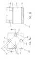
- FIG. 2illustrates a cross-sectional side view of a partially formed integrated circuit in accordance with one or more embodiments of the invention.
- FIG. 2Aillustrates a top view of a partially formed integrated circuit in accordance with one or more embodiments of the invention.
- FIG. 2Billustrates a cross-sectional side view of the partially formed integrated circuit of FIG. 2A along the sectional line 2 B shown in FIG. 2A .
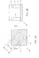
- FIG. 3Aillustrates a top view of the partially formed integrated circuit of FIG. 2A after the pattern of pillars has been trimmed in accordance with one or more embodiments of the invention.
- FIG. 3Billustrates a cross-sectional side view of the partially formed integrated circuit of FIG. 3A along the sectional line 3 B shown in FIG. 3A .
- FIG. 4Aillustrates a top view of the partially formed integrated circuit of FIG. 3A after transferring the pattern of pillars to underlying masking layers in accordance with one or more embodiments of the invention.
- FIG. 4Billustrates a cross-sectional side view of the partially formed integrated circuit of FIG. 4A along the sectional line 4 B shown in FIG. 4A .
- FIG. 5Aillustrates a top view of the partially formed integrated circuit of FIG. 4A after one of the masking layers has been removed in accordance with one or more embodiments of the invention.
- FIG. 5Billustrates a cross-sectional side view of the partially formed integrated circuit of FIG. 5A along the sectional line 5 B shown in FIG. 5A .
- FIG. 6Aillustrates a top view of the partially formed integrated circuit of FIG. 5A during deposition of a spacer material on pillars in accordance with one or more embodiments of the invention.
- FIG. 6Billustrates a cross-sectional side view of the partially formed integrated circuit of FIG. 6A along the sectional line 6 B shown in FIG. 6A .
- FIG. 7Aillustrates a top view of the partially formed integrated circuit of FIG. 6A after deposition of the spacer material in accordance with one or more embodiments of the invention.
- FIG. 7Billustrates a cross-sectional side view of the partially formed integrated circuit of FIG. 7A along the sectional line 7 B shown in FIG. 7A .
- FIG. 8Aillustrates a top view of the partially formed integrated circuit of FIG. 7A after etching the spacer material in accordance with one or more embodiments of the invention.
- FIG. 8Billustrates a cross-sectional side view of the partially formed integrated circuit of FIG. 8A along the sectional line 8 B shown in FIG. 8A .
- FIG. 9Aillustrates a top view of the partially formed integrated circuit of FIG. 8A after further etching the spacer material in accordance with one or more embodiments of the invention.
- FIG. 9Billustrates a cross-sectional side view of the partially formed integrated circuit of FIG. 9A along the sectional line 9 B shown in FIG. 9A .
- FIG. 10Aillustrates a top view of the partially formed integrated circuit of FIG. 9A after etching the pillars in accordance with one or more embodiments of the invention.
- FIG. 10Billustrates a cross-sectional side view of the partially formed integrated circuit of FIG. 10A along the sectional line 10 B shown in FIG. 10A .
- FIG. 11Aillustrates a top view of the partially formed integrated circuit of FIG. 10A after forming plugs in accordance with one or more embodiments of the invention.
- FIG. 11Billustrates a cross-sectional side view of the partially formed integrated circuit of FIG. 11A along the sectional line 11 B shown in FIG. 11A .
- FIG. 12Aillustrates a top view of the partially formed integrated circuit of FIG. 11 A after removing the spacer material in accordance with one or more embodiments of the invention.
- FIG. 12Billustrates a cross-sectional side view of the partially formed integrated circuit of FIG. 12A along the sectional line 12 B shown in FIG. 12A .
- Embodiments described hereinprovide methods of forming patterns of isolated features having a high density.
- a methodfor forming an integrated circuit with a pattern of features having a final density of features that is greater than a starting density of features in the integrated circuit by a multiple of two or more.
- the methodcan include forming a pattern of isolated pillars having a density X.
- the methodcan further include forming spacers around the pillars, such as by blanket depositing spacer material on and around the pillars and then isotropically etching the spacer materials to form a pattern of holes having a density at least about X.
- the pillarscan be selectively removed to form a mask with a pattern of holes having a density at least about 2X.
- plugscan be formed in the pattern of holes in the mask, such as by epitaxial deposition on the substrate, in order to provide a pattern of pillars having a density at least 2X.
- the pattern of holes in the maskcan be etched into the substrate to provide a pattern of holes in the substrate.
- FIG. 1Aillustrates a general sequence of process steps according to some embodiments of the invention.
- a plurality of pillarsare formed on a substrate, such as by etching into a layer or stack of layers formed over the substrate or by forming material over a substrate in a pattern that defines a plurality of pillars.
- the pillarscan be formed by photolithography, by selectively exposing photoresist to light and then developing the photoresist to leave a pattern of pillars formed by the photoresist.
- “forming” a structureincludes performing steps to make the structure or providing the structure already premade.
- step 3spacer material is formed on and around the pillars to fill spaces between the pillars while leaving a pattern of openings between the pillars.
- step 5the spacer material is etched to form a pattern of holes completely open to an underlying material, the holes having a density at least as great as the density of the pattern of pillars.
- step 7the pillars are removed to form further holes, thus providing a pattern of holes with a density at least twice as great as the pattern of pillars that were previously formed on the substrate.
- FIGS. 1B-12Billustrate schematically a detailed sequence of process steps according to some embodiments of the invention.
- a substrate 100is provided and a first hard mask layer 110 is formed thereover.
- FIG. 2illustrates a partially formed integrated circuit 200 after step 12 has been carried out.
- the substrate 100may include one or more of a variety of suitable workpieces for semiconductor processing.
- the substratecan include a silicon wafer.
- the first hard mask layer 110includes amorphous carbon, e.g., transparent carbon, which has been found to have excellent etch selectivity with other materials of the illustrated imaging or masking stack. Methods for forming amorphous carbon are disclosed in A. Helmbold, D.
- a second hard mask layer 112is also formed over the first hard mask layer 110 to protect the first hard mask layer 110 during etching in later steps and/or to enhance the accuracy of forming patterns by photolithography.
- the second hard mask layer 112includes an anti-reflective coating (ARC), such as DARC or BARC/DARC, which can facilitate photolithography by preventing undesired light reflections.
- ARCanti-reflective coating
- a selectively definable layer 120is formed on the second hard mask layer 112 .
- the selectively definable layer 120can be formed using a photoresist in accordance with well-known processes for providing masks in semiconductor fabrication.
- the photoresistcan be any photoresist compatible with 157 nm, 193 nm, 248 nm or 365 nm wavelength systems, 193 nm wavelength immersion systems, extreme ultraviolet systems (including 13.7 nm wavelength systems) or electron beam lithographic systems.
- maskless lithography, or maskless photolithographycan be used to define the selectively definable layer 120 .
- photoresist materialsinclude argon fluoride (ArF) sensitive photoresist, i.e., photoresist suitable for use with an ArF light source, and krypton fluoride (KrF) sensitive photoresist, i.e., photoresist suitable for use with a KrF light source.
- ArF photoresistsare preferably used with photolithography systems utilizing relatively short wavelength light, e.g., 193 nm.
- KrF photoresistsare preferably used with longer wavelength photolithography systems, such as 248 nm systems.
- the selectively definable layer 120 and any subsequent resist layerscan be formed of a resist that can be patterned by nano-imprint lithography, e.g., by using a mold or mechanical force to pattern the resist.
- FIGS. 2A and 2Billustrate a partially formed integrated circuit 200 after step 12 has been carried out.
- the selectively definable layer 120can include a mask pattern, the pattern including a plurality of pillars 121 having a substantially circular cross-section.
- the width of the pillars 121 in the selectively definable layer 120is A.
- the pillars 121can be patterned using a photolithographic technique.
- Acan be substantially equal to the minimum feature size formable using the lithographic techniques.
- the pillars 121can be formed with width A larger than the minimum formable feature size formed by photolithography and subsequently trimmed, in order to enhance the accuracy of the patterns formed by photolithography. It will be appreciated that photolithographic techniques typically can more easily and accurately form features having sizes above the size limit of the technique.
- the distance between centers of nearest neighboring pillars 121is B.
- Bis substantially equal to twice the width A, which has advantages for forming a pattern of holes arranged in rows and columns as described herein.
- the pillars 121 of the selectively definable layer 120are trimmed during the trimming step 14 in order to achieve the dimensions C, D, and E as described hereinbelow.
- the mask pattern shown in FIGS. 2A and 2Bincludes pillars 121 with their centers located at the corner points of a square, other patterns are also possible, as will be described more fully hereinbelow.
- FIGS. 3A and 3Billustrate the partially formed integrated circuit 200 after step 14 of FIG. 1B has been carried out.
- the selectively definable layer 120is trimmed, such as by subjecting the selectively definable layer 120 to O 2 /Cl 2 or O 2 /HBr plasma.
- FIG. 3Bshows that after the trimming step 14 , the pillars 121 of the selectively definable layer 120 have a width C, which is less than the width A.
- the trimming step 14can advantageously provide a feature size that is less than the minimum feature size formable using the lithographic technique used to pattern the selectively definable layer 120 .
- the width Cis substantially equal to
- FIG. 3Balso shows that after the trimming step 14 , the distance between two distant pillars 121 of the selectively definable layer 120 , such as between pillars 121 a and 121 c , is E.
- the distance Eis substantially equal to
- FIG. 3Ashows that after the trimming step 14 , the distance between neighboring pillars 121 of the selectively definable layer 120 , such as between pillars 121 a and 121 b, is D.
- the distance Dis substantially equal to
- Yis used herein as a multiplier having a dimension of distance to clarify the relationship between various dimensions in the pattern of one or more embodiments.
- Cis substantially equal to
- Ycan be any real number greater than zero, including the minimum feature size formable using known lithographic techniques, and does not necessarily bear any relationship to the width A of the pillars 121 after step 12 .
- Selectively definable layers 120 having a pattern of these dimensionscan produce a pattern of spacer-defined holes in later steps that is advantageously aligned with the pattern of pillars 121 in the selectively definable layer 120 .
- the pattern of the selectively definable layer 120 shown in FIG. 3Acan be described as a set of pillars 121 formed in columns and rows, in which the leftmost pillar 121 a is positioned in a first column and a second row, the uppermost pillar 121 b is positioned in the second column and the first row, the lowermost pillar 121 d is positioned in the second column and a third row, and the rightmost pillar 121 c is positioned in the third column and the second row.
- FIG. 8Ashows a pattern of holes 140 with a hole 140 a positioned in the first column and the first row, another hole 140 d positioned in the first column and the third row, another hole 140 c positioned in the second column and the second row, another hole 140 b positioned in the third column and the first row, and another hole 140 e positioned in the third column and the third row.
- step 16 of FIG. 1Bthe pattern of pillars 121 of the selectively definable layer 120 is transferred to the second hard mask layer 112 , such as by anisotropically etching the second hard mask layer 112 through the selectively definable layer 120 .
- FIGS. 4A and 4Billustrate the partially formed integrated circuit 200 after step 20 of FIG. 1B has been carried out.
- step 20pillars 122 are formed in the first hard mask layer 110 by anisotropically etching the first hard mask layer 110 through the selectively definable layer 120 and the second hard mask layer 112 .
- the pillars 122 formed in step 20can have substantially the same pattern as the pattern in the selectively definable layer 120 .
- the selectively definable layer 120can be removed during or after the etching step 20 .
- the second hard mask layer 112may be removed in step 22 , such as by carrying out a wet strip etch.
- the selectively definable layer 120is removed by the same etch used to define pillars 122 in the first hard mask layer 110 .
- FIGS. 5A and 5Billustrate the partially formed integrated circuit 200 after removing the selectively definable layer 120 .
- spacer material 130( FIGS. 6A , 6 B) is deposited on the pillars 122 .
- FIGS. 6A and 6Billustrate the partially formed integrated circuit 200 while step 30 of FIG. 1B is being carried out.
- the spacer materialcan include an insulating material, such as an oxide, e.g., silicon oxide, particularly a material that is selectively etchable with respect to the material of the pillars 122 and other exposed surfaces. Examples of other spacer materials include silicon nitride, Al 2 O 3 , TiN, etc.
- depositing step 30includes uniformly depositing spacer material 130 on the pillars 122 and the substrate 100 , such as by blanket depositing the spacer material 130 by chemical vapor deposition.
- FIGS. 6A and 6Bshow that as spacer material 130 is deposited on the pillars 122 , the spacer material 130 fills a space between neighboring pillars 122 when the spacer material 130 forms a layer having a thickness F.
- the thickness Fis substantially equal to
- spacer material 130continues to be deposited beyond filling the space between the nearest neighboring pillars 122 , such that the spacer material 130 surrounding the nearest neighboring pillars 122 converge and form voids with substantially circular cross-sections.
- the rate of deposition at the corners formed by the convergenceis greater than at other parts between the pillars 122 , causing the corners of the open space between the pillars 122 to become rounded.
- FIGS. 7A and 7Billustrate the partially formed integrated circuit 200 after depositing step 30 has been carried out.
- sufficient spacer material 130has been deposited to form holes 140 with a substantially circular cross-section.
- the holes 140occur in a pattern that is aligned with the pattern of the pillars 122 , as described above, and the density of the holes is greater than the density of the pillars 122 in the illustrated portion of the partially formed integrated circuit.
- FIGS. 8A and 8Billustrate the partially formed integrated circuit 200 after step 32 of FIG. 1B has been carried out. As shown in FIG. 8B , after any etching to expand the holes 140 , the layer of the spacer material 130 has a thickness G and the holes 140 have been expanded to form holes 141 having a width H.
- the width H and the thickness Gare both substantially equal to the width C of the pillars 122 , advantageously providing a pattern of holes 141 and pillars 122 of substantially the same size. Steps 30 and 32 of FIG. 1B can be repeated as desired in order to achieve holes 141 of the desired shapes and sizes.
- spacer material 130( FIGS. 9A , 9 B) is anisotropically etched to expose the upper surfaces of the pillars 122 and the substrate 100 .
- FIGS. 9A and 9Billustrate the partially formed integrated circuit 200 after step 34 of FIG. 1B has been carried out.
- the width H of the holes 141 and the thickness G of the spacer material 130 between the holes 141 and the pillars 122remain substantially the same as before step 34 .
- the order of steps 32 and 34can be reversed, such that the spacer material 130 is anisotropically etched before being trimmed by, e.g., an isotropic etch. In such embodiments, holes having different widths may be formed.
- step 40 of FIG. 1Bthe pillars 122 ( FIGS. 9A , 9 B) are etched, such as by selectively etching the first hard mask layer 110 relative to the spacer material 130 to remove the pillars 122 .
- FIGS. 10A and 10Billustrate the partially formed integrated circuit 200 after step 40 of FIG. 1B has been carried out. At this stage, a pattern of holes 141 has been achieved that has a density greater than or equal to about twice the density of the features that were formed in the selectively definable layer 120 .
- the holes 141have a smaller feature size than the pillars 121 first formed by photolithography in the selectively definable layer 120 , and the holes 141 occur in a pattern that is aligned with the pattern of pillars 121 in the selectively definable layer 120 .
- plugs 150are formed in the holes 141 .
- FIGS. 11A and 11Billustrate the partially formed integrated circuit 200 after step 50 of FIG. 1B has been carried out.
- Plugs 150can be formed of the same material as the substrate 100 .
- the spacer material 130is chosen to be selectively etchable relative to the material forming the plugs 150 .
- the plugs 150are formed of polysilicon and the spacer material 130 is formed of silicon oxide.
- Depositing step 50can be carried out in accordance with well-known deposition processes, including but not limited to chemical vapor deposition (CVD), plasma enhanced chemical vapor deposition (PECVD), or spin coating.
- plugs 150FIGS. 11A and 11B
- step 60the spacer material 130 ( FIGS. 11A , 11 B) is removed, such as by selectively etching the spacer material 130 .
- the spacer material 130FIGS. 11A , 11 B
- FIGS. 12A and 12Billustrate the partially formed integrated circuit 200 after step 60 has been carried out.
- a pattern of plugs 150has been formed on the substrate 100 with a density greater than or equal to about twice the density of the pillars that were formed on the selectively definable layer 120 .
- the plugs 150have a smaller feature size than the pillars 121 first formed on the selectively definable layer 120 , and the plugs 150 occur in a pattern that is aligned with the pattern of pillars 121 in the selectively definable layer 120 .
- the method described abovecan provide a pattern of plugs with a density greater than or equal to about twice the density of the features that were formed on the selectively definable layer 120
- the methodmay also be repeated to produce a pattern with a density of features that is greater than or equal to about four times the density of the original pattern.
- the methodmay then be repeated to achieve a pattern with a density of features that is greater than or equal to about eight times the density of the original pattern, and so on until the desired density is reached.
- the plugs 150 or pillars patterned in the substrate 100using the layer 130 ( FIGS. 10A and 10B ) as a mask, can be used as the pillars 122 in subsequent repeats of the method.
- steps 30 - 60may be repeated.
- isolated features having a density 2 ncan be formed, where n is the number of times the method of FIGS. 1A and 1B is repeated.
- holes 141 and pillars 122have the same size in the method described above, it may be desirable in some applications to form holes that are larger or smaller than the pillars. Accordingly, the thickness of the spacer material can be adjusted to achieve the desired result.
- the method described aboveprovides pillars and holes with a generally circular cross section
- other shapesare also possible.
- the pillars and holescan have a cross section that is generally in the shape of a square, a rectangle, or an ellipse.
- the method described aboveprovides holes 140 in a pattern that is aligned with the pattern of the pillars 122 , it is also possible to place the holes in other locations relative to the pillars by beginning with a pattern of pillars other than the one described above, for example a pattern in which the centers of the pillars occur at the corners of a square.
- a pattern of pillarsother than the one described above, for example a pattern in which the centers of the pillars occur at the corners of a square.
- Another pattern that can be usedis a pattern of three pillars, which can be used to form a hole between the three pillars.
- the embodiments described abovecan be used to selectively create patterns with higher density in some regions of the integrated circuit but not in other regions.
- featurescan be spaced apart at a distance sufficiently small that it can be filled by the thickness of the spacer material.
- featurescan be spaced apart at too great a distance to be filled by the spacer material and/or selectively a protective mask can be used to prevent transfer of a pattern formed by the spacer material to the substrate 110 , or to prevent deposition in the same openings formed by the spacer material 130 . In this way, a high density pattern can be selectively provided in some regions of the integrated circuit but not in others.
- an imaging stack including photoresist, an ARC, and amorphous carboncan be advantageously be applied to facilitate deposition of the spacer material. Temperatures typically used for chemical vapor deposition of the spacer material may undesirably deform photoresist, thus, amorphous carbon is used to form the pillars upon which the spacer material is deposited. In other embodiments where low temperature deposition processes (e.g., atomic layer deposition) are used to deposit the spacer material, the ARC and amorphous carbon layers may be omitted and the spacer material can be deposited on pillars formed of photoresist.
- low temperature deposition processese.g., atomic layer deposition
- a methodis provided. Such a method might include, for example, providing a substrate and forming a first set of pillars on the substrate. The method can further include depositing spacer material on the first set of pillars to form a first pattern of holes, wherein at least one of the holes is located between pillars of the first set and wherein, after depositing, spacer material fills a space between a first pillar of the first set and a nearest neighboring pillar of the first set.
- a methodin other embodiments, can include providing a substrate and forming a plurality of pillars on the substrate, the pillars having a density X.
- the methodcan further include blanket depositing material on the pillars to form a pattern of holes on a level of the pillars, the holes having a density at least X.
- a methodis provided.
- the methodcan include providing a substrate and forming a set of pillars on the substrate, wherein the pillars have a width of about
- the methodcan further include depositing material on the set of pillars.
- the methodcan further include etching the material to form a pattern of holes, wherein the pattern comprises a hole between the first pillar and the third pillar.
- a methodcan include providing a set of pillars on a substrate, the pillars arranged in two or more rows and two or more columns.
- the methodcan further include blanket depositing spacer material on the set of pillars to form a pattern of holes adjacent the pillars.
- the methodcan further include isotropically etching the spacer material to enlarge the width of the holes.
- the methodcan further include anisotropically etching the spacer material to expose the pillars.
Landscapes
- Engineering & Computer Science (AREA)
- Microelectronics & Electronic Packaging (AREA)
- Condensed Matter Physics & Semiconductors (AREA)
- General Physics & Mathematics (AREA)
- Manufacturing & Machinery (AREA)
- Computer Hardware Design (AREA)
- Physics & Mathematics (AREA)
- Power Engineering (AREA)
- Chemical & Material Sciences (AREA)
- Inorganic Chemistry (AREA)
- Internal Circuitry In Semiconductor Integrated Circuit Devices (AREA)
- Drying Of Semiconductors (AREA)
- Semiconductor Memories (AREA)
Abstract
Description
- This application is a continuation of U.S. patent application Ser. No. 11/952,017, filed Dec. 6, 2007, the disclosure of which is hereby incorporated by reference in its entirety herein.
- 1. Field of the Invention
- Embodiments of the invention relate to semiconductor processing, and more particularly to masking techniques.
- 2. Description of the Related Art
- There is a constant demand for faster and smaller integrated circuits, faster and smaller integrated circuits may be made by reducing the sizes and separation distances between the individual elements or electronic devices forming an integrated circuit. This process of increasing the density of circuit elements across a substrate is typically referred to as “scaling.” As a result of the demand for faster and smaller integrated circuits, there is a constant need for methods of scaling to form isolated features with a high density.
- The appended drawings are schematic, not necessarily drawn to scale, and are meant to illustrate and not to limit embodiments of the invention.
FIG. 1A is a flow chart illustrating a process in accordance with one or more embodiments of the invention.FIG. 1B is another flow chart illustrating a process in accordance with one or more embodiments of the invention.FIG. 2 illustrates a cross-sectional side view of a partially formed integrated circuit in accordance with one or more embodiments of the invention.FIG. 2A illustrates a top view of a partially formed integrated circuit in accordance with one or more embodiments of the invention.FIG. 2B illustrates a cross-sectional side view of the partially formed integrated circuit ofFIG. 2A along thesectional line 2B shown inFIG. 2A .FIG. 3A illustrates a top view of the partially formed integrated circuit ofFIG. 2A after the pattern of pillars has been trimmed in accordance with one or more embodiments of the invention.FIG. 3B illustrates a cross-sectional side view of the partially formed integrated circuit ofFIG. 3A along thesectional line 3B shown inFIG. 3A .FIG. 4A illustrates a top view of the partially formed integrated circuit ofFIG. 3A after transferring the pattern of pillars to underlying masking layers in accordance with one or more embodiments of the invention.FIG. 4B illustrates a cross-sectional side view of the partially formed integrated circuit ofFIG. 4A along thesectional line 4B shown inFIG. 4A .FIG. 5A illustrates a top view of the partially formed integrated circuit ofFIG. 4A after one of the masking layers has been removed in accordance with one or more embodiments of the invention.FIG. 5B illustrates a cross-sectional side view of the partially formed integrated circuit ofFIG. 5A along thesectional line 5B shown inFIG. 5A .FIG. 6A illustrates a top view of the partially formed integrated circuit ofFIG. 5A during deposition of a spacer material on pillars in accordance with one or more embodiments of the invention.FIG. 6B illustrates a cross-sectional side view of the partially formed integrated circuit ofFIG. 6A along thesectional line 6B shown inFIG. 6A .FIG. 7A illustrates a top view of the partially formed integrated circuit ofFIG. 6A after deposition of the spacer material in accordance with one or more embodiments of the invention.FIG. 7B illustrates a cross-sectional side view of the partially formed integrated circuit ofFIG. 7A along thesectional line 7B shown inFIG. 7A .FIG. 8A illustrates a top view of the partially formed integrated circuit ofFIG. 7A after etching the spacer material in accordance with one or more embodiments of the invention.FIG. 8B illustrates a cross-sectional side view of the partially formed integrated circuit ofFIG. 8A along thesectional line 8B shown inFIG. 8A .FIG. 9A illustrates a top view of the partially formed integrated circuit ofFIG. 8A after further etching the spacer material in accordance with one or more embodiments of the invention.FIG. 9B illustrates a cross-sectional side view of the partially formed integrated circuit ofFIG. 9A along thesectional line 9B shown inFIG. 9A .FIG. 10A illustrates a top view of the partially formed integrated circuit ofFIG. 9A after etching the pillars in accordance with one or more embodiments of the invention.FIG. 10B illustrates a cross-sectional side view of the partially formed integrated circuit ofFIG. 10A along thesectional line 10B shown inFIG. 10A .FIG. 11A illustrates a top view of the partially formed integrated circuit ofFIG. 10A after forming plugs in accordance with one or more embodiments of the invention.FIG. 11B illustrates a cross-sectional side view of the partially formed integrated circuit ofFIG. 11A along thesectional line 11B shown inFIG. 11A .FIG. 12A illustrates a top view of the partially formed integrated circuit ofFIG. 11 A after removing the spacer material in accordance with one or more embodiments of the invention.FIG. 12B illustrates a cross-sectional side view of the partially formed integrated circuit ofFIG. 12A along thesectional line 12B shown inFIG. 12A .- Embodiments described herein provide methods of forming patterns of isolated features having a high density. In one or more embodiments, a method is provided for forming an integrated circuit with a pattern of features having a final density of features that is greater than a starting density of features in the integrated circuit by a multiple of two or more. The method can include forming a pattern of isolated pillars having a density X. The method can further include forming spacers around the pillars, such as by blanket depositing spacer material on and around the pillars and then isotropically etching the spacer materials to form a pattern of holes having a density at least about X. The pillars can be selectively removed to form a mask with a pattern of holes having a density at least about 2X. In some embodiments, plugs can be formed in the pattern of holes in the mask, such as by epitaxial deposition on the substrate, in order to provide a pattern of pillars having a density at least 2X. In other embodiments, the pattern of holes in the mask can be etched into the substrate to provide a pattern of holes in the substrate.
- Reference will now be made to the figures, in which like numerals refer to like parts throughout.
FIG. 1A illustrates a general sequence of process steps according to some embodiments of the invention. Instep 1 ofFIG. 1A , a plurality of pillars are formed on a substrate, such as by etching into a layer or stack of layers formed over the substrate or by forming material over a substrate in a pattern that defines a plurality of pillars. For example, the pillars can be formed by photolithography, by selectively exposing photoresist to light and then developing the photoresist to leave a pattern of pillars formed by the photoresist. As used herein, “forming” a structure includes performing steps to make the structure or providing the structure already premade. In step3, spacer material is formed on and around the pillars to fill spaces between the pillars while leaving a pattern of openings between the pillars. Instep 5, the spacer material is etched to form a pattern of holes completely open to an underlying material, the holes having a density at least as great as the density of the pattern of pillars. Instep 7, the pillars are removed to form further holes, thus providing a pattern of holes with a density at least twice as great as the pattern of pillars that were previously formed on the substrate.FIGS. 1B-12B illustrate schematically a detailed sequence of process steps according to some embodiments of the invention. Instep 10, asubstrate 100 is provided and a firsthard mask layer 110 is formed thereover. (FIG. 2 illustrates a partially formedintegrated circuit 200 afterstep 12 has been carried out.) Thesubstrate 100 may include one or more of a variety of suitable workpieces for semiconductor processing. For example, the substrate can include a silicon wafer. In one or more embodiments, the firsthard mask layer 110 includes amorphous carbon, e.g., transparent carbon, which has been found to have excellent etch selectivity with other materials of the illustrated imaging or masking stack. Methods for forming amorphous carbon are disclosed in A. Helmbold, D. Meissner, Thin Solid Films, 283 (1996) 196-203 and U.S. Patent Application Publication No. 2006/0211260, published Sep. 21, 2006, entitled “PITCH REDUCED PATTERNS RELATIVE TO PHOTOLITHOGRAPHY FEATURES,” the entire disclosures of which are hereby incorporated herein by reference. In the illustrated embodiment, a secondhard mask layer 112 is also formed over the firsthard mask layer 110 to protect the firsthard mask layer 110 during etching in later steps and/or to enhance the accuracy of forming patterns by photolithography. In one or more embodiments, the secondhard mask layer 112 includes an anti-reflective coating (ARC), such as DARC or BARC/DARC, which can facilitate photolithography by preventing undesired light reflections.- In
step 12, a selectivelydefinable layer 120 is formed on the secondhard mask layer 112. The selectivelydefinable layer 120 can be formed using a photoresist in accordance with well-known processes for providing masks in semiconductor fabrication. For example, the photoresist can be any photoresist compatible with 157 nm, 193 nm, 248 nm or 365 nm wavelength systems, 193 nm wavelength immersion systems, extreme ultraviolet systems (including 13.7 nm wavelength systems) or electron beam lithographic systems. In addition, maskless lithography, or maskless photolithography, can be used to define the selectivelydefinable layer 120. Examples of preferred photoresist materials include argon fluoride (ArF) sensitive photoresist, i.e., photoresist suitable for use with an ArF light source, and krypton fluoride (KrF) sensitive photoresist, i.e., photoresist suitable for use with a KrF light source. ArF photoresists are preferably used with photolithography systems utilizing relatively short wavelength light, e.g., 193 nm. KrF photoresists are preferably used with longer wavelength photolithography systems, such as 248 nm systems. In other embodiments, the selectivelydefinable layer 120 and any subsequent resist layers can be formed of a resist that can be patterned by nano-imprint lithography, e.g., by using a mold or mechanical force to pattern the resist.FIGS. 2A and 2B illustrate a partially formedintegrated circuit 200 afterstep 12 has been carried out. As shown inFIGS. 2A and 2B , the selectivelydefinable layer 120 can include a mask pattern, the pattern including a plurality ofpillars 121 having a substantially circular cross-section. The width of thepillars 121 in the selectivelydefinable layer 120 is A. Thepillars 121 can be patterned using a photolithographic technique. In one or more embodiments, A can be substantially equal to the minimum feature size formable using the lithographic techniques. In other embodiments, thepillars 121 can be formed with width A larger than the minimum formable feature size formed by photolithography and subsequently trimmed, in order to enhance the accuracy of the patterns formed by photolithography. It will be appreciated that photolithographic techniques typically can more easily and accurately form features having sizes above the size limit of the technique. - As shown in
FIG. 2A , the distance between centers of nearestneighboring pillars 121, such as betweenpillars pillars 121 of the selectivelydefinable layer 120 are trimmed during the trimmingstep 14 in order to achieve the dimensions C, D, and E as described hereinbelow. Although the mask pattern shown inFIGS. 2A and 2B includespillars 121 with their centers located at the corner points of a square, other patterns are also possible, as will be described more fully hereinbelow. FIGS. 3A and 3B illustrate the partially formedintegrated circuit 200 afterstep 14 ofFIG. 1B has been carried out. Instep 14, the selectivelydefinable layer 120 is trimmed, such as by subjecting the selectivelydefinable layer 120 to O2/Cl2or O2/HBr plasma.FIG. 3B shows that after the trimmingstep 14, thepillars 121 of the selectivelydefinable layer 120 have a width C, which is less than the width A. Thus, the trimmingstep 14 can advantageously provide a feature size that is less than the minimum feature size formable using the lithographic technique used to pattern the selectivelydefinable layer 120. In one or more embodiments, the width C is substantially equal toFIG. 3B also shows that after the trimmingstep 14, the distance between twodistant pillars 121 of the selectivelydefinable layer 120, such as betweenpillars FIG. 3A shows that after the trimmingstep 14, the distance between neighboringpillars 121 of the selectivelydefinable layer 120, such as betweenpillars - Y is used herein as a multiplier having a dimension of distance to clarify the relationship between various dimensions in the pattern of one or more embodiments. Although C is substantially equal to
- in
FIGS. 3A and 3B , Y can be any real number greater than zero, including the minimum feature size formable using known lithographic techniques, and does not necessarily bear any relationship to the width A of thepillars 121 afterstep 12. - Selectively
definable layers 120 having a pattern of these dimensions can produce a pattern of spacer-defined holes in later steps that is advantageously aligned with the pattern ofpillars 121 in the selectivelydefinable layer 120. In particular, the pattern of the selectivelydefinable layer 120 shown inFIG. 3A can be described as a set ofpillars 121 formed in columns and rows, in which theleftmost pillar 121ais positioned in a first column and a second row, theuppermost pillar 121bis positioned in the second column and the first row, thelowermost pillar 121dis positioned in the second column and a third row, and therightmost pillar 121cis positioned in the third column and the second row. When the mask pattern is formed using the dimensions described above, the holes formed in later steps can advantageously be positioned in open positions in the same columns and rows, such that the pattern of holes is aligned with the pattern of pillars.FIG. 8A , described more fully below, shows a pattern ofholes 140 with a hole140apositioned in the first column and the first row, another hole140dpositioned in the first column and the third row, another hole140cpositioned in the second column and the second row, another hole140bpositioned in the third column and the first row, and another hole140epositioned in the third column and the third row. - In
step 16 ofFIG. 1B , the pattern ofpillars 121 of the selectivelydefinable layer 120 is transferred to the secondhard mask layer 112, such as by anisotropically etching the secondhard mask layer 112 through the selectivelydefinable layer 120. FIGS. 4A and 4B illustrate the partially formedintegrated circuit 200 afterstep 20 ofFIG. 1B has been carried out. Instep 20,pillars 122 are formed in the firsthard mask layer 110 by anisotropically etching the firsthard mask layer 110 through the selectivelydefinable layer 120 and the secondhard mask layer 112. As shown inFIGS. 4A and 4B , thepillars 122 formed instep 20 can have substantially the same pattern as the pattern in the selectivelydefinable layer 120. The selectivelydefinable layer 120 can be removed during or after theetching step 20. In embodiments including the secondhard mask layer 112, the secondhard mask layer 112 may be removed instep 22, such as by carrying out a wet strip etch. In other embodiments, the selectivelydefinable layer 120 is removed by the same etch used to definepillars 122 in the firsthard mask layer 110.FIGS. 5A and 5B illustrate the partially formedintegrated circuit 200 after removing the selectivelydefinable layer 120.- In
step 30 ofFIG. 1B , spacer material130 (FIGS. 6A ,6B) is deposited on thepillars 122.FIGS. 6A and 6B illustrate the partially formedintegrated circuit 200 whilestep 30 ofFIG. 1B is being carried out. The spacer material can include an insulating material, such as an oxide, e.g., silicon oxide, particularly a material that is selectively etchable with respect to the material of thepillars 122 and other exposed surfaces. Examples of other spacer materials include silicon nitride, Al2O3, TiN, etc. In one or more embodiments, depositingstep 30 includes uniformly depositingspacer material 130 on thepillars 122 and thesubstrate 100, such as by blanket depositing thespacer material 130 by chemical vapor deposition. FIGS. 6A and 6B show that asspacer material 130 is deposited on thepillars 122, thespacer material 130 fills a space between neighboringpillars 122 when thespacer material 130 forms a layer having a thickness F. In one or more embodiments, the thickness F is substantially equal to- Preferably,
spacer material 130 continues to be deposited beyond filling the space between the nearest neighboringpillars 122, such that thespacer material 130 surrounding the nearest neighboringpillars 122 converge and form voids with substantially circular cross-sections. Advantageously, due to corners having a relatively higher surface area for interacting with precursors, it has been found that the rate of deposition at the corners formed by the convergence is greater than at other parts between thepillars 122, causing the corners of the open space between thepillars 122 to become rounded. FIGS. 7A and 7B illustrate the partially formedintegrated circuit 200 after depositingstep 30 has been carried out. As shown inFIGS. 7A and 7B ,sufficient spacer material 130 has been deposited to formholes 140 with a substantially circular cross-section. Theholes 140 occur in a pattern that is aligned with the pattern of thepillars 122, as described above, and the density of the holes is greater than the density of thepillars 122 in the illustrated portion of the partially formed integrated circuit.- In order to achieve a rounded cross-section for the
holes 140, it may be necessary to deposit somuch spacer material 130 that the width of theholes 140 is smaller than the width C of the pillars. Instep 32 ofFIG. 1B , thespacer material 130 can be trimmed, such as by isotropically etching to uniformly expand the width of theholes 140.FIGS. 8A and 8B illustrate the partially formedintegrated circuit 200 afterstep 32 ofFIG. 1B has been carried out. As shown inFIG. 8B , after any etching to expand theholes 140, the layer of thespacer material 130 has a thickness G and theholes 140 have been expanded to formholes 141 having a width H. In one or more embodiments, the width H and the thickness G are both substantially equal to the width C of thepillars 122, advantageously providing a pattern ofholes 141 andpillars 122 of substantially the same size.Steps FIG. 1B can be repeated as desired in order to achieveholes 141 of the desired shapes and sizes. - In
step 34 ofFIG. 1B , spacer material130 (FIGS. 9A ,9B) is anisotropically etched to expose the upper surfaces of thepillars 122 and thesubstrate 100.FIGS. 9A and 9B illustrate the partially formedintegrated circuit 200 afterstep 34 ofFIG. 1B has been carried out. The width H of theholes 141 and the thickness G of thespacer material 130 between theholes 141 and thepillars 122 remain substantially the same as beforestep 34. In some embodiments, the order ofsteps spacer material 130 is anisotropically etched before being trimmed by, e.g., an isotropic etch. In such embodiments, holes having different widths may be formed. - In
step 40 ofFIG. 1B , the pillars122 (FIGS. 9A ,9B) are etched, such as by selectively etching the firsthard mask layer 110 relative to thespacer material 130 to remove thepillars 122.FIGS. 10A and 10B illustrate the partially formedintegrated circuit 200 afterstep 40 ofFIG. 1B has been carried out. At this stage, a pattern ofholes 141 has been achieved that has a density greater than or equal to about twice the density of the features that were formed in the selectivelydefinable layer 120. Moreover, theholes 141 have a smaller feature size than thepillars 121 first formed by photolithography in the selectivelydefinable layer 120, and theholes 141 occur in a pattern that is aligned with the pattern ofpillars 121 in the selectivelydefinable layer 120. - In
step 50 ofFIG. 1B , plugs150 (FIGS. 11A ,11B) are formed in theholes 141.FIGS. 11A and 11B illustrate the partially formedintegrated circuit 200 afterstep 50 ofFIG. 1B has been carried out.Plugs 150 can be formed of the same material as thesubstrate 100. Thespacer material 130 is chosen to be selectively etchable relative to the material forming theplugs 150. In one or more embodiments, theplugs 150 are formed of polysilicon and thespacer material 130 is formed of silicon oxide. Depositingstep 50 can be carried out in accordance with well-known deposition processes, including but not limited to chemical vapor deposition (CVD), plasma enhanced chemical vapor deposition (PECVD), or spin coating. In some embodiments, plugs150 (FIGS. 11A and 11B ) can be formed by epitaxial growth. - In
step 60, the spacer material130 (FIGS. 11A ,11B) is removed, such as by selectively etching thespacer material 130. In processes using spin coating, CVD or PECVD instep 50 to deposit theplugs 150, it may be necessary to first planarize the surface, such as by a chemical mechanical polishing process, or perform a plug material etch back process in order to expose thespacer material 130. FIGS. 12A and 12B illustrate the partially formedintegrated circuit 200 afterstep 60 has been carried out. A pattern ofplugs 150 has been formed on thesubstrate 100 with a density greater than or equal to about twice the density of the pillars that were formed on the selectivelydefinable layer 120. Moreover, theplugs 150 have a smaller feature size than thepillars 121 first formed on the selectivelydefinable layer 120, and theplugs 150 occur in a pattern that is aligned with the pattern ofpillars 121 in the selectivelydefinable layer 120.- While the method described above can provide a pattern of plugs with a density greater than or equal to about twice the density of the features that were formed on the selectively
definable layer 120, the method may also be repeated to produce a pattern with a density of features that is greater than or equal to about four times the density of the original pattern. The method may then be repeated to achieve a pattern with a density of features that is greater than or equal to about eight times the density of the original pattern, and so on until the desired density is reached. For example, it will be appreciated that theplugs 150 or pillars patterned in thesubstrate 100, using the layer130 (FIGS. 10A and 10B ) as a mask, can be used as thepillars 122 in subsequent repeats of the method. For example, after forming these pillars steps30-60 may be repeated. Thus, isolated features having a density 2ncan be formed, where n is the number of times the method ofFIGS. 1A and 1B is repeated. - Many variations of the embodiments described herein are possible. For example, while the
holes 141 andpillars 122 have the same size in the method described above, it may be desirable in some applications to form holes that are larger or smaller than the pillars. Accordingly, the thickness of the spacer material can be adjusted to achieve the desired result. - Additionally, while the method described above provides pillars and holes with a generally circular cross section, other shapes are also possible. For example, the pillars and holes can have a cross section that is generally in the shape of a square, a rectangle, or an ellipse.
- Further, while the method described above provides
holes 140 in a pattern that is aligned with the pattern of thepillars 122, it is also possible to place the holes in other locations relative to the pillars by beginning with a pattern of pillars other than the one described above, for example a pattern in which the centers of the pillars occur at the corners of a square. One example of another pattern that can be used is a pattern of three pillars, which can be used to form a hole between the three pillars. - Moreover, the embodiments described above can be used to selectively create patterns with higher density in some regions of the integrated circuit but not in other regions. In regions where a new, higher density pattern is to be formed, features can be spaced apart at a distance sufficiently small that it can be filled by the thickness of the spacer material. In regions where a higher density pattern is not desired, features can be spaced apart at too great a distance to be filled by the spacer material and/or selectively a protective mask can be used to prevent transfer of a pattern formed by the spacer material to the
substrate 110, or to prevent deposition in the same openings formed by thespacer material 130. In this way, a high density pattern can be selectively provided in some regions of the integrated circuit but not in others. - In addition, it will be appreciated the use of an imaging stack including photoresist, an ARC, and amorphous carbon can be advantageously be applied to facilitate deposition of the spacer material. Temperatures typically used for chemical vapor deposition of the spacer material may undesirably deform photoresist, thus, amorphous carbon is used to form the pillars upon which the spacer material is deposited. In other embodiments where low temperature deposition processes (e.g., atomic layer deposition) are used to deposit the spacer material, the ARC and amorphous carbon layers may be omitted and the spacer material can be deposited on pillars formed of photoresist.
- In accordance with the embodiments described above, a method is provided. Such a method might include, for example, providing a substrate and forming a first set of pillars on the substrate. The method can further include depositing spacer material on the first set of pillars to form a first pattern of holes, wherein at least one of the holes is located between pillars of the first set and wherein, after depositing, spacer material fills a space between a first pillar of the first set and a nearest neighboring pillar of the first set.
- In other embodiments, a method is provided. The method can include providing a substrate and forming a plurality of pillars on the substrate, the pillars having a density X. The method can further include blanket depositing material on the pillars to form a pattern of holes on a level of the pillars, the holes having a density at least X.
- In other embodiments, a method is provided. The method can include providing a substrate and forming a set of pillars on the substrate, wherein the pillars have a width of about
- and wherein a first pillar is separated from a second pillar by a distance of about
- and wherein the first pillar is separated from a third pillar by a distance of about
- The method can further include depositing material on the set of pillars. The method can further include etching the material to form a pattern of holes, wherein the pattern comprises a hole between the first pillar and the third pillar.
- In other embodiments, a method is provided. The method can include providing a set of pillars on a substrate, the pillars arranged in two or more rows and two or more columns. The method can further include blanket depositing spacer material on the set of pillars to form a pattern of holes adjacent the pillars. The method can further include isotropically etching the spacer material to enlarge the width of the holes. The method can further include anisotropically etching the spacer material to expose the pillars.
- It will be appreciated by those skilled in the art that various other omissions, additions, and modifications may be made to the methods and structures described above without departing from the scope of the invention. All such changes are intended to fall within the scope of the invention, as defined by the appended claims.
Claims (20)
Priority Applications (2)
| Application Number | Priority Date | Filing Date | Title |
|---|---|---|---|
| US12/686,602US8324107B2 (en) | 2007-12-06 | 2010-01-13 | Method for forming high density patterns |
| US13/690,266US8871648B2 (en) | 2007-12-06 | 2012-11-30 | Method for forming high density patterns |
Applications Claiming Priority (2)
| Application Number | Priority Date | Filing Date | Title |
|---|---|---|---|
| US11/952,017US7659208B2 (en) | 2007-12-06 | 2007-12-06 | Method for forming high density patterns |
| US12/686,602US8324107B2 (en) | 2007-12-06 | 2010-01-13 | Method for forming high density patterns |
Related Parent Applications (1)
| Application Number | Title | Priority Date | Filing Date |
|---|---|---|---|
| US11/952,017ContinuationUS7659208B2 (en) | 2007-12-06 | 2007-12-06 | Method for forming high density patterns |
Related Child Applications (1)
| Application Number | Title | Priority Date | Filing Date |
|---|---|---|---|
| US13/690,266ContinuationUS8871648B2 (en) | 2007-12-06 | 2012-11-30 | Method for forming high density patterns |
Publications (2)
| Publication Number | Publication Date |
|---|---|
| US20100112818A1true US20100112818A1 (en) | 2010-05-06 |
| US8324107B2 US8324107B2 (en) | 2012-12-04 |
Family
ID=40722113
Family Applications (3)
| Application Number | Title | Priority Date | Filing Date |
|---|---|---|---|
| US11/952,017Active2028-01-24US7659208B2 (en) | 2007-12-06 | 2007-12-06 | Method for forming high density patterns |
| US12/686,602Active2029-02-08US8324107B2 (en) | 2007-12-06 | 2010-01-13 | Method for forming high density patterns |
| US13/690,266ActiveUS8871648B2 (en) | 2007-12-06 | 2012-11-30 | Method for forming high density patterns |
Family Applications Before (1)
| Application Number | Title | Priority Date | Filing Date |
|---|---|---|---|
| US11/952,017Active2028-01-24US7659208B2 (en) | 2007-12-06 | 2007-12-06 | Method for forming high density patterns |
Family Applications After (1)
| Application Number | Title | Priority Date | Filing Date |
|---|---|---|---|
| US13/690,266ActiveUS8871648B2 (en) | 2007-12-06 | 2012-11-30 | Method for forming high density patterns |
Country Status (6)
| Country | Link |
|---|---|
| US (3) | US7659208B2 (en) |
| EP (1) | EP2232530A4 (en) |
| KR (1) | KR101564474B1 (en) |
| CN (1) | CN101889326B (en) |
| TW (1) | TWI505324B (en) |
| WO (1) | WO2009075959A1 (en) |
Cited By (2)
| Publication number | Priority date | Publication date | Assignee | Title |
|---|---|---|---|---|
| CN102811166A (en)* | 2011-05-31 | 2012-12-05 | 三星Sds株式会社 | Method and apparatus for controlling flow to receive data in parallel |
| US20160276153A1 (en)* | 2013-10-01 | 2016-09-22 | Taiwan Semiconductor Manufacturing Company, Ltd. | Self-Aligned Patterning Process |
Families Citing this family (40)
| Publication number | Priority date | Publication date | Assignee | Title |
|---|---|---|---|---|
| US7923373B2 (en) | 2007-06-04 | 2011-04-12 | Micron Technology, Inc. | Pitch multiplication using self-assembling materials |
| US7659208B2 (en)* | 2007-12-06 | 2010-02-09 | Micron Technology, Inc | Method for forming high density patterns |
| US7759201B2 (en)* | 2007-12-17 | 2010-07-20 | Sandisk 3D Llc | Method for fabricating pitch-doubling pillar structures |
| US7790531B2 (en) | 2007-12-18 | 2010-09-07 | Micron Technology, Inc. | Methods for isolating portions of a loop of pitch-multiplied material and related structures |
| US7887999B2 (en)* | 2007-12-27 | 2011-02-15 | Sandisk 3D Llc | Method of making a pillar pattern using triple or quadruple exposure |
| US8030218B2 (en) | 2008-03-21 | 2011-10-04 | Micron Technology, Inc. | Method for selectively modifying spacing between pitch multiplied structures |
| US7981592B2 (en) | 2008-04-11 | 2011-07-19 | Sandisk 3D Llc | Double patterning method |
| US7786015B2 (en)* | 2008-04-28 | 2010-08-31 | Sandisk 3D Llc | Method for fabricating self-aligned complementary pillar structures and wiring |
| US7781269B2 (en)* | 2008-06-30 | 2010-08-24 | Sandisk 3D Llc | Triangle two dimensional complementary patterning of pillars |
| US7732235B2 (en)* | 2008-06-30 | 2010-06-08 | Sandisk 3D Llc | Method for fabricating high density pillar structures by double patterning using positive photoresist |
| US8076208B2 (en) | 2008-07-03 | 2011-12-13 | Micron Technology, Inc. | Method for forming transistor with high breakdown voltage using pitch multiplication technique |
| US8659165B2 (en)* | 2008-08-12 | 2014-02-25 | Texas Instruments Incorporated | Contact and VIA interconnects using metal around dielectric pillars |
| US8076056B2 (en)* | 2008-10-06 | 2011-12-13 | Sandisk 3D Llc | Method of making sub-resolution pillar structures using undercutting technique |
| US8492282B2 (en) | 2008-11-24 | 2013-07-23 | Micron Technology, Inc. | Methods of forming a masking pattern for integrated circuits |
| KR20100083581A (en)* | 2009-01-14 | 2010-07-22 | 삼성전자주식회사 | Methods of forming semiconductor device |
| JP5330004B2 (en)* | 2009-02-03 | 2013-10-30 | 株式会社東芝 | Manufacturing method of semiconductor device |
| EP2287669A1 (en)* | 2009-06-26 | 2011-02-23 | Rohm and Haas Electronic Materials, L.L.C. | Methods of forming electronic devices |
| US8026178B2 (en)* | 2010-01-12 | 2011-09-27 | Sandisk 3D Llc | Patterning method for high density pillar structures |
| US7923305B1 (en) | 2010-01-12 | 2011-04-12 | Sandisk 3D Llc | Patterning method for high density pillar structures |
| US8900988B2 (en) | 2011-04-15 | 2014-12-02 | International Business Machines Corporation | Method for forming self-aligned airgap interconnect structures |
| US8890318B2 (en) | 2011-04-15 | 2014-11-18 | International Business Machines Corporation | Middle of line structures |
| US9054160B2 (en) | 2011-04-15 | 2015-06-09 | International Business Machines Corporation | Interconnect structure and method for fabricating on-chip interconnect structures by image reversal |
| US8822137B2 (en)* | 2011-08-03 | 2014-09-02 | International Business Machines Corporation | Self-aligned fine pitch permanent on-chip interconnect structures and method of fabrication |
| US20130062732A1 (en) | 2011-09-08 | 2013-03-14 | International Business Machines Corporation | Interconnect structures with functional components and methods for fabrication |
| US9087753B2 (en) | 2012-05-10 | 2015-07-21 | International Business Machines Corporation | Printed transistor and fabrication method |
| KR102015568B1 (en) | 2012-08-27 | 2019-08-28 | 삼성전자주식회사 | A method for forming a semiconductor memory device |
| KR102037874B1 (en) | 2013-02-07 | 2019-10-29 | 삼성전자주식회사 | Method of Forming Hole patterns of Semiconductor Devices |
| US8802551B1 (en) | 2013-02-21 | 2014-08-12 | Samsung Electronics Co., Ltd. | Methods of fabricating a semiconductor device using voids in a sacrificial layer |
| US9177797B2 (en)* | 2013-12-04 | 2015-11-03 | Taiwan Semiconductor Manufacturing Company, Ltd. | Lithography using high selectivity spacers for pitch reduction |
| US9184059B2 (en)* | 2014-03-21 | 2015-11-10 | Inotera Memories, Inc. | Method for increasing pattern density |
| KR20160085043A (en)* | 2015-01-07 | 2016-07-15 | 에스케이하이닉스 주식회사 | Method for fabricating pattern |
| TWI640042B (en) | 2015-03-09 | 2018-11-01 | 聯華電子股份有限公司 | Manufacturing method of patterned structure of semiconductor device |
| KR102325201B1 (en) | 2015-04-22 | 2021-11-11 | 삼성전자주식회사 | Methods of manufacturing semiconductor devices |
| KR102274738B1 (en) | 2016-01-08 | 2021-07-07 | 삼성전자주식회사 | Semiconductor device and method for fabricating the same |
| CN105800549B (en)* | 2016-01-16 | 2018-08-21 | 苏州工业园区纳米产业技术研究院有限公司 | Metallic nanodots array and the method for being used to form nano dot device |
| US11067895B2 (en) | 2017-01-13 | 2021-07-20 | International Business Machines Corporation | Method and structures for personalizing lithography |
| US10283362B2 (en)* | 2017-08-17 | 2019-05-07 | Nanya Technology Corporation | Method of forming fine line patterns of semiconductor devices |
| US10204783B1 (en)* | 2017-09-03 | 2019-02-12 | Nanya Technology Corporation | Method of forming fine island patterns of semiconductor devices |
| US10115594B1 (en)* | 2017-09-05 | 2018-10-30 | Nanya Technology Corporation | Method of forming fine island patterns of semiconductor devices |
| US11114299B2 (en)* | 2019-07-05 | 2021-09-07 | Applied Materials, Inc. | Techniques for reducing tip to tip shorting and critical dimension variation during nanoscale patterning |
Citations (25)
| Publication number | Priority date | Publication date | Assignee | Title |
|---|---|---|---|---|
| US4803181A (en)* | 1986-03-27 | 1989-02-07 | International Business Machines Corporation | Process for forming sub-micrometer patterns using silylation of resist side walls |
| US5593813A (en)* | 1994-07-14 | 1997-01-14 | Hyundai Electronics Industries Co. Ltd. | Method for forming submicroscopic patterns |
| US5858620A (en)* | 1996-07-05 | 1999-01-12 | Mitsubishi Denki Kabushiki Kaisha | Semiconductor device and method for manufacturing the same |
| US6020255A (en)* | 1998-07-13 | 2000-02-01 | Taiwan Semiconductor Manufacturing Company | Dual damascene interconnect process with borderless contact |
| US6207490B1 (en)* | 1997-12-11 | 2001-03-27 | Samsung Electronics Co., Ltd. | Semiconductor device and method for fabricating the same |
| US20020094688A1 (en)* | 2001-01-16 | 2002-07-18 | Semiconductor Leading Edge Technologies, Inc. | Method of forming fine patterns |
| US6620715B1 (en)* | 2002-03-29 | 2003-09-16 | Cypress Semiconductor Corp. | Method for forming sub-critical dimension structures in an integrated circuit |
| US6762449B2 (en)* | 1999-04-23 | 2004-07-13 | Hitachi, Ltd. | Semiconductor integrated circuit device and the process of manufacturing the same having poly-silicon plug, wiring trenches and bit lines formed in the wiring trenches having a width finer than a predetermined size |
| US6818141B1 (en)* | 2002-06-10 | 2004-11-16 | Advanced Micro Devices, Inc. | Application of the CVD bilayer ARC as a hard mask for definition of the subresolution trench features between polysilicon wordlines |
| US6916594B2 (en)* | 2002-12-30 | 2005-07-12 | Hynix Semiconductor Inc. | Overcoating composition for photoresist and method for forming photoresist pattern using the same |
| US6955961B1 (en)* | 2004-05-27 | 2005-10-18 | Macronix International Co., Ltd. | Method for defining a minimum pitch in an integrated circuit beyond photolithographic resolution |
| US20060011947A1 (en)* | 2004-05-26 | 2006-01-19 | Werner Juengling | Semiconductor structures and memory device constructions |
| US20060115978A1 (en)* | 2004-11-30 | 2006-06-01 | Michael Specht | Charge-trapping memory cell and method for production |
| US20070077524A1 (en)* | 2005-09-30 | 2007-04-05 | Samsung Electronics Co., Ltd. | Method for forming patterns of semiconductor device |
| US7202174B1 (en)* | 2006-02-02 | 2007-04-10 | Hynix Semiconductor Inc. | Method of forming micro pattern in semiconductor device |
| US7271107B2 (en)* | 2005-02-03 | 2007-09-18 | Lam Research Corporation | Reduction of feature critical dimensions using multiple masks |
| US20080054350A1 (en)* | 2006-09-06 | 2008-03-06 | International Business Machines Corporation | Vertical field effect transistor arrays and methods for fabrication thereof |
| US7378727B2 (en)* | 2005-09-30 | 2008-05-27 | Dirk Caspary | Memory device and a method of forming a memory device |
| US7393789B2 (en)* | 2005-09-01 | 2008-07-01 | Micron Technology, Inc. | Protective coating for planarization |
| US7442976B2 (en)* | 2004-09-01 | 2008-10-28 | Micron Technology, Inc. | DRAM cells with vertical transistors |
| US7456458B2 (en)* | 2006-01-11 | 2008-11-25 | Promos Technologies Inc. | Dynamic random access memory structure |
| US20080292991A1 (en)* | 2007-05-24 | 2008-11-27 | Advanced Micro Devices, Inc. | High fidelity multiple resist patterning |
| US7537866B2 (en)* | 2006-05-24 | 2009-05-26 | Synopsys, Inc. | Patterning a single integrated circuit layer using multiple masks and multiple masking layers |
| US7659205B2 (en)* | 2004-07-27 | 2010-02-09 | Micron Technology, Inc. | Amorphous carbon-based non-volatile memory |
| US7851135B2 (en)* | 2007-11-30 | 2010-12-14 | Hynix Semiconductor Inc. | Method of forming an etching mask pattern from developed negative and positive photoresist layers |
Family Cites Families (169)
| Publication number | Priority date | Publication date | Assignee | Title |
|---|---|---|---|---|
| JPS5748237Y2 (en) | 1978-12-28 | 1982-10-22 | ||
| US4234362A (en) | 1978-11-03 | 1980-11-18 | International Business Machines Corporation | Method for forming an insulator between layers of conductive material |
| US4508579A (en) | 1981-03-30 | 1985-04-02 | International Business Machines Corporation | Lateral device structures using self-aligned fabrication techniques |
| US4432132A (en) | 1981-12-07 | 1984-02-21 | Bell Telephone Laboratories, Incorporated | Formation of sidewall oxide layers by reactive oxygen ion etching to define submicron features |
| US4419809A (en) | 1981-12-30 | 1983-12-13 | International Business Machines Corporation | Fabrication process of sub-micrometer channel length MOSFETs |
| DE3242113A1 (en) | 1982-11-13 | 1984-05-24 | Ibm Deutschland Gmbh, 7000 Stuttgart | METHOD FOR PRODUCING A THIN DIELECTRIC INSULATION IN A SILICON SEMICONDUCTOR BODY |
| US4716131A (en) | 1983-11-28 | 1987-12-29 | Nec Corporation | Method of manufacturing semiconductor device having polycrystalline silicon layer with metal silicide film |
| US4648937A (en) | 1985-10-30 | 1987-03-10 | International Business Machines Corporation | Method of preventing asymmetric etching of lines in sub-micrometer range sidewall images transfer |
| GB8528967D0 (en) | 1985-11-25 | 1986-01-02 | Plessey Co Plc | Semiconductor device manufacture |
| US5514885A (en) | 1986-10-09 | 1996-05-07 | Myrick; James J. | SOI methods and apparatus |
| JP2805702B2 (en)* | 1987-07-24 | 1998-09-30 | ソニー株式会社 | Semiconductor memory device |
| JPS6435916U (en) | 1987-08-28 | 1989-03-03 | ||
| US4776922A (en) | 1987-10-30 | 1988-10-11 | International Business Machines Corporation | Formation of variable-width sidewall structures |
| US4838991A (en) | 1987-10-30 | 1989-06-13 | International Business Machines Corporation | Process for defining organic sidewall structures |
| US5328810A (en) | 1990-05-07 | 1994-07-12 | Micron Technology, Inc. | Method for reducing, by a factor or 2-N, the minimum masking pitch of a photolithographic process |
| US5013680A (en) | 1990-07-18 | 1991-05-07 | Micron Technology, Inc. | Process for fabricating a DRAM array having feature widths that transcend the resolution limit of available photolithography |
| US5053105A (en) | 1990-07-19 | 1991-10-01 | Micron Technology, Inc. | Process for creating an etch mask suitable for deep plasma etches employing self-aligned silicidation of a metal layer masked with a silicon dioxide template |
| DE4034612A1 (en) | 1990-10-31 | 1992-05-07 | Huels Chemische Werke Ag | METHOD FOR PRODUCING ORGANOSILANES CONTAINING METHACRYLOXY OR ACRYLOXY GROUPS |
| IT1243919B (en) | 1990-11-20 | 1994-06-28 | Cons Ric Microelettronica | PROCEDURE FOR OBTAINING PLANARIZED SUBMICHROMETRIC GROOVES IN INTEGRATED CIRCUITS REALIZED WITH ULSI TECHNOLOGY |
| JPH05343370A (en) | 1992-06-10 | 1993-12-24 | Toshiba Corp | Method of forming fine pattern |
| US5330879A (en) | 1992-07-16 | 1994-07-19 | Micron Technology, Inc. | Method for fabrication of close-tolerance lines and sharp emission tips on a semiconductor wafer |
| DE4236609A1 (en) | 1992-10-29 | 1994-05-05 | Siemens Ag | Method for forming a structure in the surface of a substrate - with an auxiliary structure laterally bounding an initial masking structure, followed by selective removal of masking structure using the auxiliary structure as an etching mask |
| US5407785A (en) | 1992-12-18 | 1995-04-18 | Vlsi Technology, Inc. | Method for generating dense lines on a semiconductor wafer using phase-shifting and multiple exposures |
| US5470661A (en) | 1993-01-07 | 1995-11-28 | International Business Machines Corporation | Diamond-like carbon films from a hydrocarbon helium plasma |
| US6042998A (en) | 1993-09-30 | 2000-03-28 | The University Of New Mexico | Method and apparatus for extending spatial frequencies in photolithography images |
| JPH0855920A (en) | 1994-08-15 | 1996-02-27 | Toshiba Corp | Method for manufacturing semiconductor device |
| JPH0855908A (en) | 1994-08-17 | 1996-02-27 | Toshiba Corp | Semiconductor device |
| US5600153A (en) | 1994-10-07 | 1997-02-04 | Micron Technology, Inc. | Conductive polysilicon lines and thin film transistors |
| TW366367B (en) | 1995-01-26 | 1999-08-11 | Ibm | Sputter deposition of hydrogenated amorphous carbon film |
| US5795830A (en) | 1995-06-06 | 1998-08-18 | International Business Machines Corporation | Reducing pitch with continuously adjustable line and space dimensions |
| KR100190757B1 (en) | 1995-06-30 | 1999-06-01 | 김영환 | Method of forming mosfet |
| JP3393286B2 (en) | 1995-09-08 | 2003-04-07 | ソニー株式会社 | Pattern formation method |
| US5789320A (en) | 1996-04-23 | 1998-08-04 | International Business Machines Corporation | Plating of noble metal electrodes for DRAM and FRAM |
| JP3164026B2 (en) | 1996-08-21 | 2001-05-08 | 日本電気株式会社 | Semiconductor device and manufacturing method thereof |
| US5933742A (en)* | 1996-09-06 | 1999-08-03 | Powerchip Semiconductor Corp. | Multi-crown capacitor for high density DRAMS |
| US5998256A (en) | 1996-11-01 | 1999-12-07 | Micron Technology, Inc. | Semiconductor processing methods of forming devices on a substrate, forming device arrays on a substrate, forming conductive lines on a substrate, and forming capacitor arrays on a substrate, and integrated circuitry |
| US6395613B1 (en) | 2000-08-30 | 2002-05-28 | Micron Technology, Inc. | Semiconductor processing methods of forming a plurality of capacitors on a substrate, bit line contacts and method of forming bit line contacts |
| US5895740A (en) | 1996-11-13 | 1999-04-20 | Vanguard International Semiconductor Corp. | Method of forming contact holes of reduced dimensions by using in-situ formed polymeric sidewall spacers |
| KR100231134B1 (en)* | 1997-06-14 | 1999-11-15 | 문정환 | Method for forming metal interconnector of semiconductor device |
| US6063688A (en) | 1997-09-29 | 2000-05-16 | Intel Corporation | Fabrication of deep submicron structures and quantum wire transistors using hard-mask transistor width definition |
| US6143476A (en) | 1997-12-12 | 2000-11-07 | Applied Materials Inc | Method for high temperature etching of patterned layers using an organic mask stack |
| US6291334B1 (en) | 1997-12-19 | 2001-09-18 | Applied Materials, Inc. | Etch stop layer for dual damascene process |
| US6004862A (en) | 1998-01-20 | 1999-12-21 | Advanced Micro Devices, Inc. | Core array and periphery isolation technique |
| JP2975917B2 (en) | 1998-02-06 | 1999-11-10 | 株式会社半導体プロセス研究所 | Semiconductor device manufacturing method and semiconductor device manufacturing apparatus |
| US5933725A (en) | 1998-05-27 | 1999-08-03 | Vanguard International Semiconductor Corporation | Word line resistance reduction method and design for high density memory with relaxed metal pitch |
| US6245662B1 (en) | 1998-07-23 | 2001-06-12 | Applied Materials, Inc. | Method of producing an interconnect structure for an integrated circuit |
| US6071789A (en) | 1998-11-10 | 2000-06-06 | Vanguard International Semiconductor Corporation | Method for simultaneously fabricating a DRAM capacitor and metal interconnections |
| US6204187B1 (en) | 1999-01-06 | 2001-03-20 | Infineon Technologies North America, Corp. | Contact and deep trench patterning |
| US6211044B1 (en) | 1999-04-12 | 2001-04-03 | Advanced Micro Devices | Process for fabricating a semiconductor device component using a selective silicidation reaction |
| US6110837A (en) | 1999-04-28 | 2000-08-29 | Worldwide Semiconductor Manufacturing Corp. | Method for forming a hard mask of half critical dimension |
| US6136662A (en) | 1999-05-13 | 2000-10-24 | Lsi Logic Corporation | Semiconductor wafer having a layer-to-layer alignment mark and method for fabricating the same |
| US6204115B1 (en)* | 1999-06-03 | 2001-03-20 | Stanford University | Manufacture of high-density pillar memory cell arrangement |
| JP2000357736A (en) | 1999-06-15 | 2000-12-26 | Toshiba Corp | Semiconductor device and manufacturing method thereof |
| JP2001077196A (en) | 1999-09-08 | 2001-03-23 | Sony Corp | Manufacture of semiconductor device |
| US6362057B1 (en) | 1999-10-26 | 2002-03-26 | Motorola, Inc. | Method for forming a semiconductor device |
| US6582891B1 (en) | 1999-12-02 | 2003-06-24 | Axcelis Technologies, Inc. | Process for reducing edge roughness in patterned photoresist |
| US6573030B1 (en) | 2000-02-17 | 2003-06-03 | Applied Materials, Inc. | Method for depositing an amorphous carbon layer |
| US6967140B2 (en) | 2000-03-01 | 2005-11-22 | Intel Corporation | Quantum wire gate device and method of making same |
| US6297554B1 (en) | 2000-03-10 | 2001-10-02 | United Microelectronics Corp. | Dual damascene interconnect structure with reduced parasitic capacitance |
| US6423474B1 (en) | 2000-03-21 | 2002-07-23 | Micron Technology, Inc. | Use of DARC and BARC in flash memory processing |
| JP3805603B2 (en) | 2000-05-29 | 2006-08-02 | 富士通株式会社 | Semiconductor device and manufacturing method thereof |
| US6632741B1 (en) | 2000-07-19 | 2003-10-14 | International Business Machines Corporation | Self-trimming method on looped patterns |
| US6455372B1 (en) | 2000-08-14 | 2002-09-24 | Micron Technology, Inc. | Nucleation for improved flash erase characteristics |
| US6348380B1 (en) | 2000-08-25 | 2002-02-19 | Micron Technology, Inc. | Use of dilute steam ambient for improvement of flash devices |
| SE517275C2 (en) | 2000-09-20 | 2002-05-21 | Obducat Ab | Wet etching of substrate involves arranging on the substrate a passivating substance comprising active substance reacting with component contained in etchant to form etch protecting compound |
| US6335257B1 (en) | 2000-09-29 | 2002-01-01 | Vanguard International Semiconductor Corporation | Method of making pillar-type structure on semiconductor substrate |
| US6667237B1 (en) | 2000-10-12 | 2003-12-23 | Vram Technologies, Llc | Method and apparatus for patterning fine dimensions |
| US6534243B1 (en) | 2000-10-23 | 2003-03-18 | Advanced Micro Devices, Inc. | Chemical feature doubling process |
| US6926843B2 (en) | 2000-11-30 | 2005-08-09 | International Business Machines Corporation | Etching of hard masks |
| US6664028B2 (en) | 2000-12-04 | 2003-12-16 | United Microelectronics Corp. | Method of forming opening in wafer layer |
| KR100399436B1 (en)* | 2001-03-28 | 2003-09-29 | 주식회사 하이닉스반도체 | A Magnetic random access memory and a method for manufacturing the same |
| US6740594B2 (en) | 2001-05-31 | 2004-05-25 | Infineon Technologies Ag | Method for removing carbon-containing polysilane from a semiconductor without stripping |
| US6960806B2 (en) | 2001-06-21 | 2005-11-01 | International Business Machines Corporation | Double gated vertical transistor with different first and second gate materials |
| US6522584B1 (en) | 2001-08-02 | 2003-02-18 | Micron Technology, Inc. | Programming methods for multi-level flash EEPROMs |
| US6744094B2 (en) | 2001-08-24 | 2004-06-01 | Micron Technology Inc. | Floating gate transistor with horizontal gate layers stacked next to vertical body |
| TW497138B (en) | 2001-08-28 | 2002-08-01 | Winbond Electronics Corp | Method for improving consistency of critical dimension |
| DE10142590A1 (en) | 2001-08-31 | 2003-04-03 | Infineon Technologies Ag | Production of resist structures used in semiconductor industry comprises applying a resist film on a substrate, forming a resist structure with bars from the film, and removing reinforced sections |
| US7045383B2 (en) | 2001-09-19 | 2006-05-16 | BAE Systems Information and Ovonyx, Inc | Method for making tapered opening for programmable resistance memory element |
| JP2003133437A (en) | 2001-10-24 | 2003-05-09 | Hitachi Ltd | Semiconductor device manufacturing method and semiconductor device |
| US7226853B2 (en) | 2001-12-26 | 2007-06-05 | Applied Materials, Inc. | Method of forming a dual damascene structure utilizing a three layer hard mask structure |
| TW576864B (en) | 2001-12-28 | 2004-02-21 | Toshiba Corp | Method for manufacturing a light-emitting device |
| US6638441B2 (en) | 2002-01-07 | 2003-10-28 | Macronix International Co., Ltd. | Method for pitch reduction |
| DE10207131B4 (en) | 2002-02-20 | 2007-12-20 | Infineon Technologies Ag | Process for forming a hardmask in a layer on a flat disk |
| US6759180B2 (en) | 2002-04-23 | 2004-07-06 | Hewlett-Packard Development Company, L.P. | Method of fabricating sub-lithographic sized line and space patterns for nano-imprinting lithography |
| US20030207584A1 (en) | 2002-05-01 | 2003-11-06 | Swaminathan Sivakumar | Patterning tighter and looser pitch geometries |
| US6951709B2 (en) | 2002-05-03 | 2005-10-04 | Micron Technology, Inc. | Method of fabricating a semiconductor multilevel interconnect structure |
| US6602779B1 (en) | 2002-05-13 | 2003-08-05 | Taiwan Semiconductor Manufacturing Co., Ltd | Method for forming low dielectric constant damascene structure while employing carbon doped silicon oxide planarizing stop layer |
| US6703312B2 (en) | 2002-05-17 | 2004-03-09 | International Business Machines Corporation | Method of forming active devices of different gatelengths using lithographic printed gate images of same length |
| US6734107B2 (en) | 2002-06-12 | 2004-05-11 | Macronix International Co., Ltd. | Pitch reduction in semiconductor fabrication |
| US6559017B1 (en) | 2002-06-13 | 2003-05-06 | Advanced Micro Devices, Inc. | Method of using amorphous carbon as spacer material in a disposable spacer process |
| KR100476924B1 (en) | 2002-06-14 | 2005-03-17 | 삼성전자주식회사 | Method Of Forming Fine Pattern Of Semiconductor Device |
| US6924191B2 (en) | 2002-06-20 | 2005-08-02 | Applied Materials, Inc. | Method for fabricating a gate structure of a field effect transistor |
| AU2003280498A1 (en) | 2002-06-27 | 2004-01-19 | Advanced Micro Devices, Inc. | Method of defining the dimensions of circuit elements by using spacer deposition techniques |
| US6835663B2 (en) | 2002-06-28 | 2004-12-28 | Infineon Technologies Ag | Hardmask of amorphous carbon-hydrogen (a-C:H) layers with tunable etch resistivity |
| US6500756B1 (en) | 2002-06-28 | 2002-12-31 | Advanced Micro Devices, Inc. | Method of forming sub-lithographic spaces between polysilicon lines |
| US6689695B1 (en) | 2002-06-28 | 2004-02-10 | Taiwan Semiconductor Manufacturing Company | Multi-purpose composite mask for dual damascene patterning |
| US20040018738A1 (en) | 2002-07-22 | 2004-01-29 | Wei Liu | Method for fabricating a notch gate structure of a field effect transistor |
| US6913871B2 (en) | 2002-07-23 | 2005-07-05 | Intel Corporation | Fabricating sub-resolution structures in planar lightwave devices |
| US6673684B1 (en) | 2002-07-31 | 2004-01-06 | Advanced Micro Devices, Inc. | Use of diamond as a hard mask material |
| US6800930B2 (en) | 2002-07-31 | 2004-10-05 | Micron Technology, Inc. | Semiconductor dice having back side redistribution layer accessed using through-silicon vias, and assemblies |
| US6764949B2 (en) | 2002-07-31 | 2004-07-20 | Advanced Micro Devices, Inc. | Method for reducing pattern deformation and photoresist poisoning in semiconductor device fabrication |
| US6939808B2 (en) | 2002-08-02 | 2005-09-06 | Applied Materials, Inc. | Undoped and fluorinated amorphous carbon film as pattern mask for metal etch |
| KR100480610B1 (en) | 2002-08-09 | 2005-03-31 | 삼성전자주식회사 | Forming method for fine patterns using silicon oxide layer |
| US6566280B1 (en) | 2002-08-26 | 2003-05-20 | Intel Corporation | Forming polymer features on a substrate |
| US6756284B2 (en) | 2002-09-18 | 2004-06-29 | Silicon Storage Technology, Inc. | Method for forming a sublithographic opening in a semiconductor process |
| US6706571B1 (en) | 2002-10-22 | 2004-03-16 | Advanced Micro Devices, Inc. | Method for forming multiple structures in a semiconductor device |
| US6888755B2 (en) | 2002-10-28 | 2005-05-03 | Sandisk Corporation | Flash memory cell arrays having dual control gates per memory cell charge storage element |
| JP4034164B2 (en) | 2002-10-28 | 2008-01-16 | 富士通株式会社 | Method for manufacturing fine pattern and method for manufacturing semiconductor device |
| US7119020B2 (en) | 2002-12-04 | 2006-10-10 | Matsushita Electric Industrial Co., Ltd. | Method for fabricating semiconductor device |
| US6686245B1 (en) | 2002-12-20 | 2004-02-03 | Motorola, Inc. | Vertical MOSFET with asymmetric gate structure |
| US7015124B1 (en) | 2003-04-28 | 2006-03-21 | Advanced Micro Devices, Inc. | Use of amorphous carbon for gate patterning |
| US6773998B1 (en) | 2003-05-20 | 2004-08-10 | Advanced Micro Devices, Inc. | Modified film stack and patterning strategy for stress compensation and prevention of pattern distortion in amorphous carbon gate patterning |
| JP4578785B2 (en) | 2003-05-21 | 2010-11-10 | ルネサスエレクトロニクス株式会社 | Manufacturing method of semiconductor device |
| US6835662B1 (en) | 2003-07-14 | 2004-12-28 | Advanced Micro Devices, Inc. | Partially de-coupled core and periphery gate module process |
| DE10345455A1 (en) | 2003-09-30 | 2005-05-04 | Infineon Technologies Ag | Method for producing a hard mask and hard mask arrangement |
| KR100536801B1 (en) | 2003-10-01 | 2005-12-14 | 동부아남반도체 주식회사 | Semiconductor device and fabrication method thereof |
| US6867116B1 (en) | 2003-11-10 | 2005-03-15 | Macronix International Co., Ltd. | Fabrication method of sub-resolution pitch for integrated circuits |
| JP2005150333A (en) | 2003-11-14 | 2005-06-09 | Sony Corp | Method of manufacturing semiconductor device |
| KR100554514B1 (en) | 2003-12-26 | 2006-03-03 | 삼성전자주식회사 | A pattern forming method and a gate forming method using the same in a semiconductor device. |
| US6998332B2 (en) | 2004-01-08 | 2006-02-14 | International Business Machines Corporation | Method of independent P and N gate length control of FET device made by sidewall image transfer technique |
| US6875703B1 (en) | 2004-01-20 | 2005-04-05 | International Business Machines Corporation | Method for forming quadruple density sidewall image transfer (SIT) structures |
| US7064078B2 (en) | 2004-01-30 | 2006-06-20 | Applied Materials | Techniques for the use of amorphous carbon (APF) for various etch and litho integration scheme |
| US8486287B2 (en) | 2004-03-19 | 2013-07-16 | The Regents Of The University Of California | Methods for fabrication of positional and compositionally controlled nanostructures on substrate |
| US7183205B2 (en) | 2004-06-08 | 2007-02-27 | Macronix International Co., Ltd. | Method of pitch dimension shrinkage |
| US7473644B2 (en) | 2004-07-01 | 2009-01-06 | Micron Technology, Inc. | Method for forming controlled geometry hardmasks including subresolution elements |
| US7074666B2 (en) | 2004-07-28 | 2006-07-11 | International Business Machines Corporation | Borderless contact structures |
| KR100704470B1 (en) | 2004-07-29 | 2007-04-10 | 주식회사 하이닉스반도체 | Method for manufacturing semiconductor device using amorphous carbon film as sacrificial hard mask |
| US7151040B2 (en) | 2004-08-31 | 2006-12-19 | Micron Technology, Inc. | Methods for increasing photo alignment margins |
| US7175944B2 (en) | 2004-08-31 | 2007-02-13 | Micron Technology, Inc. | Prevention of photoresist scumming |
| US7910288B2 (en) | 2004-09-01 | 2011-03-22 | Micron Technology, Inc. | Mask material conversion |
| US7655387B2 (en) | 2004-09-02 | 2010-02-02 | Micron Technology, Inc. | Method to align mask patterns |
| US7115525B2 (en) | 2004-09-02 | 2006-10-03 | Micron Technology, Inc. | Method for integrated circuit fabrication using pitch multiplication |
| KR100614651B1 (en) | 2004-10-11 | 2006-08-22 | 삼성전자주식회사 | Apparatus and method for exposing a circuit pattern, photomask used and design method thereof, lighting system and implementation method thereof |
| US7208379B2 (en) | 2004-11-29 | 2007-04-24 | Texas Instruments Incorporated | Pitch multiplication process |
| KR100596795B1 (en) | 2004-12-16 | 2006-07-05 | 주식회사 하이닉스반도체 | Capacitors for Semiconductor Devices and Method of Forming Them |
| US7183142B2 (en) | 2005-01-13 | 2007-02-27 | International Business Machines Corporation | FinFETs with long gate length at high density |
| KR100787352B1 (en) | 2005-02-23 | 2007-12-18 | 주식회사 하이닉스반도체 | Composition for hard mask and pattern formation method of semiconductor device using same |
| US7390746B2 (en) | 2005-03-15 | 2008-06-24 | Micron Technology, Inc. | Multiple deposition for integration of spacers in pitch multiplication process |
| US7253118B2 (en) | 2005-03-15 | 2007-08-07 | Micron Technology, Inc. | Pitch reduced patterns relative to photolithography features |
| US7611944B2 (en) | 2005-03-28 | 2009-11-03 | Micron Technology, Inc. | Integrated circuit fabrication |
| KR100640639B1 (en) | 2005-04-19 | 2006-10-31 | 삼성전자주식회사 | Semiconductor device including fine contact and manufacturing method thereof |
| US7429536B2 (en)* | 2005-05-23 | 2008-09-30 | Micron Technology, Inc. | Methods for forming arrays of small, closely spaced features |
| US7547599B2 (en) | 2005-05-26 | 2009-06-16 | Micron Technology, Inc. | Multi-state memory cell |
| US7560390B2 (en) | 2005-06-02 | 2009-07-14 | Micron Technology, Inc. | Multiple spacer steps for pitch multiplication |
| US7396781B2 (en) | 2005-06-09 | 2008-07-08 | Micron Technology, Inc. | Method and apparatus for adjusting feature size and position |
| JP2006351861A (en) | 2005-06-16 | 2006-12-28 | Toshiba Corp | Manufacturing method of semiconductor device |
| TW200705541A (en) | 2005-07-25 | 2007-02-01 | Li Bing Huan | Manufacturing method of nano-sticker |
| US7413981B2 (en) | 2005-07-29 | 2008-08-19 | Micron Technology, Inc. | Pitch doubled circuit layout |
| US7291560B2 (en) | 2005-08-01 | 2007-11-06 | Infineon Technologies Ag | Method of production pitch fractionizations in semiconductor technology |
| US7816262B2 (en) | 2005-08-30 | 2010-10-19 | Micron Technology, Inc. | Method and algorithm for random half pitched interconnect layout with constant spacing |
| US7829262B2 (en) | 2005-08-31 | 2010-11-09 | Micron Technology, Inc. | Method of forming pitch multipled contacts |
| US7572572B2 (en) | 2005-09-01 | 2009-08-11 | Micron Technology, Inc. | Methods for forming arrays of small, closely spaced features |
| US7687342B2 (en) | 2005-09-01 | 2010-03-30 | Micron Technology, Inc. | Method of manufacturing a memory device |
| US7759197B2 (en) | 2005-09-01 | 2010-07-20 | Micron Technology, Inc. | Method of forming isolated features using pitch multiplication |
| US7776744B2 (en) | 2005-09-01 | 2010-08-17 | Micron Technology, Inc. | Pitch multiplication spacers and methods of forming the same |
| KR100714305B1 (en) | 2005-12-26 | 2007-05-02 | 삼성전자주식회사 | Formation method of self-aligned double pattern |
| US7842558B2 (en) | 2006-03-02 | 2010-11-30 | Micron Technology, Inc. | Masking process for simultaneously patterning separate regions |
| US20070210449A1 (en) | 2006-03-07 | 2007-09-13 | Dirk Caspary | Memory device and an array of conductive lines and methods of making the same |
| US7351666B2 (en) | 2006-03-17 | 2008-04-01 | International Business Machines Corporation | Layout and process to contact sub-lithographic structures |
| US7902074B2 (en) | 2006-04-07 | 2011-03-08 | Micron Technology, Inc. | Simplified pitch doubling process flow |
| US8003310B2 (en) | 2006-04-24 | 2011-08-23 | Micron Technology, Inc. | Masking techniques and templates for dense semiconductor fabrication |
| US7488685B2 (en) | 2006-04-25 | 2009-02-10 | Micron Technology, Inc. | Process for improving critical dimension uniformity of integrated circuit arrays |
| US7795149B2 (en) | 2006-06-01 | 2010-09-14 | Micron Technology, Inc. | Masking techniques and contact imprint reticles for dense semiconductor fabrication |
| US7611980B2 (en) | 2006-08-30 | 2009-11-03 | Micron Technology, Inc. | Single spacer process for multiplying pitch by a factor greater than two and related intermediate IC structures |
| US7666578B2 (en) | 2006-09-14 | 2010-02-23 | Micron Technology, Inc. | Efficient pitch multiplication process |
| US7923373B2 (en) | 2007-06-04 | 2011-04-12 | Micron Technology, Inc. | Pitch multiplication using self-assembling materials |
| US8563229B2 (en) | 2007-07-31 | 2013-10-22 | Micron Technology, Inc. | Process of semiconductor fabrication with mask overlay on pitch multiplied features and associated structures |
| US7737039B2 (en) | 2007-11-01 | 2010-06-15 | Micron Technology, Inc. | Spacer process for on pitch contacts and related structures |
| US7659208B2 (en)* | 2007-12-06 | 2010-02-09 | Micron Technology, Inc | Method for forming high density patterns |
- 2007
- 2007-12-06USUS11/952,017patent/US7659208B2/enactiveActive
- 2008
- 2008-10-28WOPCT/US2008/081474patent/WO2009075959A1/enactiveApplication Filing
- 2008-10-28CNCN200880119291.9Apatent/CN101889326B/enactiveActive
- 2008-10-28KRKR1020107014880Apatent/KR101564474B1/enactiveActive
- 2008-10-28EPEP08858925.4Apatent/EP2232530A4/ennot_activeWithdrawn
- 2008-11-11TWTW097143566Apatent/TWI505324B/enactive
- 2010
- 2010-01-13USUS12/686,602patent/US8324107B2/enactiveActive
- 2012
- 2012-11-30USUS13/690,266patent/US8871648B2/enactiveActive
Patent Citations (25)
| Publication number | Priority date | Publication date | Assignee | Title |
|---|---|---|---|---|
| US4803181A (en)* | 1986-03-27 | 1989-02-07 | International Business Machines Corporation | Process for forming sub-micrometer patterns using silylation of resist side walls |
| US5593813A (en)* | 1994-07-14 | 1997-01-14 | Hyundai Electronics Industries Co. Ltd. | Method for forming submicroscopic patterns |
| US5858620A (en)* | 1996-07-05 | 1999-01-12 | Mitsubishi Denki Kabushiki Kaisha | Semiconductor device and method for manufacturing the same |
| US6207490B1 (en)* | 1997-12-11 | 2001-03-27 | Samsung Electronics Co., Ltd. | Semiconductor device and method for fabricating the same |
| US6020255A (en)* | 1998-07-13 | 2000-02-01 | Taiwan Semiconductor Manufacturing Company | Dual damascene interconnect process with borderless contact |
| US6762449B2 (en)* | 1999-04-23 | 2004-07-13 | Hitachi, Ltd. | Semiconductor integrated circuit device and the process of manufacturing the same having poly-silicon plug, wiring trenches and bit lines formed in the wiring trenches having a width finer than a predetermined size |
| US20020094688A1 (en)* | 2001-01-16 | 2002-07-18 | Semiconductor Leading Edge Technologies, Inc. | Method of forming fine patterns |
| US6620715B1 (en)* | 2002-03-29 | 2003-09-16 | Cypress Semiconductor Corp. | Method for forming sub-critical dimension structures in an integrated circuit |
| US6818141B1 (en)* | 2002-06-10 | 2004-11-16 | Advanced Micro Devices, Inc. | Application of the CVD bilayer ARC as a hard mask for definition of the subresolution trench features between polysilicon wordlines |
| US6916594B2 (en)* | 2002-12-30 | 2005-07-12 | Hynix Semiconductor Inc. | Overcoating composition for photoresist and method for forming photoresist pattern using the same |
| US20060011947A1 (en)* | 2004-05-26 | 2006-01-19 | Werner Juengling | Semiconductor structures and memory device constructions |
| US6955961B1 (en)* | 2004-05-27 | 2005-10-18 | Macronix International Co., Ltd. | Method for defining a minimum pitch in an integrated circuit beyond photolithographic resolution |
| US7659205B2 (en)* | 2004-07-27 | 2010-02-09 | Micron Technology, Inc. | Amorphous carbon-based non-volatile memory |
| US7442976B2 (en)* | 2004-09-01 | 2008-10-28 | Micron Technology, Inc. | DRAM cells with vertical transistors |
| US20060115978A1 (en)* | 2004-11-30 | 2006-06-01 | Michael Specht | Charge-trapping memory cell and method for production |
| US7271107B2 (en)* | 2005-02-03 | 2007-09-18 | Lam Research Corporation | Reduction of feature critical dimensions using multiple masks |
| US7393789B2 (en)* | 2005-09-01 | 2008-07-01 | Micron Technology, Inc. | Protective coating for planarization |
| US7378727B2 (en)* | 2005-09-30 | 2008-05-27 | Dirk Caspary | Memory device and a method of forming a memory device |
| US20070077524A1 (en)* | 2005-09-30 | 2007-04-05 | Samsung Electronics Co., Ltd. | Method for forming patterns of semiconductor device |
| US7456458B2 (en)* | 2006-01-11 | 2008-11-25 | Promos Technologies Inc. | Dynamic random access memory structure |
| US7202174B1 (en)* | 2006-02-02 | 2007-04-10 | Hynix Semiconductor Inc. | Method of forming micro pattern in semiconductor device |
| US7537866B2 (en)* | 2006-05-24 | 2009-05-26 | Synopsys, Inc. | Patterning a single integrated circuit layer using multiple masks and multiple masking layers |
| US20080054350A1 (en)* | 2006-09-06 | 2008-03-06 | International Business Machines Corporation | Vertical field effect transistor arrays and methods for fabrication thereof |
| US20080292991A1 (en)* | 2007-05-24 | 2008-11-27 | Advanced Micro Devices, Inc. | High fidelity multiple resist patterning |
| US7851135B2 (en)* | 2007-11-30 | 2010-12-14 | Hynix Semiconductor Inc. | Method of forming an etching mask pattern from developed negative and positive photoresist layers |
Cited By (4)
| Publication number | Priority date | Publication date | Assignee | Title |
|---|---|---|---|---|
| CN102811166A (en)* | 2011-05-31 | 2012-12-05 | 三星Sds株式会社 | Method and apparatus for controlling flow to receive data in parallel |
| US9059936B2 (en) | 2011-05-31 | 2015-06-16 | Samsung Sds Co., Ltd. | Method and apparatus for controlling stream to receive data in parallel |
| US20160276153A1 (en)* | 2013-10-01 | 2016-09-22 | Taiwan Semiconductor Manufacturing Company, Ltd. | Self-Aligned Patterning Process |
| US10049878B2 (en)* | 2013-10-01 | 2018-08-14 | Taiwan Semiconductor Manufacturing Company, Ltd. | Self-aligned patterning process |
Also Published As
| Publication number | Publication date |
|---|---|
| US8324107B2 (en) | 2012-12-04 |
| US20090149026A1 (en) | 2009-06-11 |
| EP2232530A4 (en) | 2014-10-22 |
| TWI505324B (en) | 2015-10-21 |
| WO2009075959A9 (en) | 2010-07-08 |
| KR20100106455A (en) | 2010-10-01 |
| TW200935497A (en) | 2009-08-16 |
| KR101564474B1 (en) | 2015-10-29 |
| WO2009075959A1 (en) | 2009-06-18 |
| EP2232530A1 (en) | 2010-09-29 |
| CN101889326B (en) | 2012-07-11 |
| US20130089977A1 (en) | 2013-04-11 |
| CN101889326A (en) | 2010-11-17 |
| US7659208B2 (en) | 2010-02-09 |
| US8871648B2 (en) | 2014-10-28 |
Similar Documents
| Publication | Publication Date | Title |
|---|---|---|
| US8324107B2 (en) | Method for forming high density patterns | |
| US7709396B2 (en) | Integral patterning of large features along with array using spacer mask patterning process flow | |
| US9633851B2 (en) | Semiconductor device including small pitch patterns | |
| KR101091298B1 (en) | Methods to reduce the critical dimension of semiconductor devices and partially fabricated semiconductor devices having reduced critical dimensions | |
| TWI651809B (en) | Feature size reduction | |
| US8211803B2 (en) | Spacer process for on pitch contacts and related structures | |
| KR101573286B1 (en) | Pitch reduction technology using alternating spacer depositions during the formation of a semiconductor device and systems including same | |
| KR20170042056A (en) | Method of forming patterns for semiconductor device | |
| WO2017053296A1 (en) | Methods of forming etch masks for sub-resolution substrate patterning | |
| JP4095588B2 (en) | Method for defining a minimum pitch that exceeds photolithographic resolution in an integrated circuit | |
| US7939451B2 (en) | Method for fabricating a pattern | |
| JPS63258020A (en) | Formation of element isolation pattern | |
| WO2024054362A1 (en) | Double patterning method of patterning a substrate | |
| CN115775726A (en) | Method for forming semiconductor structure |
Legal Events
| Date | Code | Title | Description |
|---|---|---|---|
| FEPP | Fee payment procedure | Free format text:PAYOR NUMBER ASSIGNED (ORIGINAL EVENT CODE: ASPN); ENTITY STATUS OF PATENT OWNER: LARGE ENTITY | |
| STCF | Information on status: patent grant | Free format text:PATENTED CASE | |
| CC | Certificate of correction | ||
| AS | Assignment | Owner name:U.S. BANK NATIONAL ASSOCIATION, AS COLLATERAL AGENT, CALIFORNIA Free format text:SECURITY INTEREST;ASSIGNOR:MICRON TECHNOLOGY, INC.;REEL/FRAME:038669/0001 Effective date:20160426 Owner name:U.S. BANK NATIONAL ASSOCIATION, AS COLLATERAL AGEN Free format text:SECURITY INTEREST;ASSIGNOR:MICRON TECHNOLOGY, INC.;REEL/FRAME:038669/0001 Effective date:20160426 | |
| FPAY | Fee payment | Year of fee payment:4 | |
| AS | Assignment | Owner name:MORGAN STANLEY SENIOR FUNDING, INC., AS COLLATERAL AGENT, MARYLAND Free format text:PATENT SECURITY AGREEMENT;ASSIGNOR:MICRON TECHNOLOGY, INC.;REEL/FRAME:038954/0001 Effective date:20160426 Owner name:MORGAN STANLEY SENIOR FUNDING, INC., AS COLLATERAL Free format text:PATENT SECURITY AGREEMENT;ASSIGNOR:MICRON TECHNOLOGY, INC.;REEL/FRAME:038954/0001 Effective date:20160426 | |
| AS | Assignment | Owner name:U.S. BANK NATIONAL ASSOCIATION, AS COLLATERAL AGENT, CALIFORNIA Free format text:CORRECTIVE ASSIGNMENT TO CORRECT THE REPLACE ERRONEOUSLY FILED PATENT #7358718 WITH THE CORRECT PATENT #7358178 PREVIOUSLY RECORDED ON REEL 038669 FRAME 0001. ASSIGNOR(S) HEREBY CONFIRMS THE SECURITY INTEREST;ASSIGNOR:MICRON TECHNOLOGY, INC.;REEL/FRAME:043079/0001 Effective date:20160426 Owner name:U.S. BANK NATIONAL ASSOCIATION, AS COLLATERAL AGEN Free format text:CORRECTIVE ASSIGNMENT TO CORRECT THE REPLACE ERRONEOUSLY FILED PATENT #7358718 WITH THE CORRECT PATENT #7358178 PREVIOUSLY RECORDED ON REEL 038669 FRAME 0001. ASSIGNOR(S) HEREBY CONFIRMS THE SECURITY INTEREST;ASSIGNOR:MICRON TECHNOLOGY, INC.;REEL/FRAME:043079/0001 Effective date:20160426 | |
| AS | Assignment | Owner name:JPMORGAN CHASE BANK, N.A., AS COLLATERAL AGENT, ILLINOIS Free format text:SECURITY INTEREST;ASSIGNORS:MICRON TECHNOLOGY, INC.;MICRON SEMICONDUCTOR PRODUCTS, INC.;REEL/FRAME:047540/0001 Effective date:20180703 Owner name:JPMORGAN CHASE BANK, N.A., AS COLLATERAL AGENT, IL Free format text:SECURITY INTEREST;ASSIGNORS:MICRON TECHNOLOGY, INC.;MICRON SEMICONDUCTOR PRODUCTS, INC.;REEL/FRAME:047540/0001 Effective date:20180703 | |
| AS | Assignment | Owner name:MICRON TECHNOLOGY, INC., IDAHO Free format text:RELEASE BY SECURED PARTY;ASSIGNOR:U.S. BANK NATIONAL ASSOCIATION, AS COLLATERAL AGENT;REEL/FRAME:047243/0001 Effective date:20180629 | |
| AS | Assignment | Owner name:MICRON TECHNOLOGY, INC., IDAHO Free format text:RELEASE BY SECURED PARTY;ASSIGNOR:MORGAN STANLEY SENIOR FUNDING, INC., AS COLLATERAL AGENT;REEL/FRAME:050937/0001 Effective date:20190731 | |
| AS | Assignment | Owner name:MICRON SEMICONDUCTOR PRODUCTS, INC., IDAHO Free format text:RELEASE BY SECURED PARTY;ASSIGNOR:JPMORGAN CHASE BANK, N.A., AS COLLATERAL AGENT;REEL/FRAME:051028/0001 Effective date:20190731 Owner name:MICRON TECHNOLOGY, INC., IDAHO Free format text:RELEASE BY SECURED PARTY;ASSIGNOR:JPMORGAN CHASE BANK, N.A., AS COLLATERAL AGENT;REEL/FRAME:051028/0001 Effective date:20190731 | |
| MAFP | Maintenance fee payment | Free format text:PAYMENT OF MAINTENANCE FEE, 8TH YEAR, LARGE ENTITY (ORIGINAL EVENT CODE: M1552); ENTITY STATUS OF PATENT OWNER: LARGE ENTITY Year of fee payment:8 | |
| MAFP | Maintenance fee payment | Free format text:PAYMENT OF MAINTENANCE FEE, 12TH YEAR, LARGE ENTITY (ORIGINAL EVENT CODE: M1553); ENTITY STATUS OF PATENT OWNER: LARGE ENTITY Year of fee payment:12 |