US20100110607A1 - Vertical capacitors and method of fabricating same - Google Patents
Vertical capacitors and method of fabricating sameDownload PDFInfo
- Publication number
- US20100110607A1 US20100110607A1US12/291,263US29126308AUS2010110607A1US 20100110607 A1US20100110607 A1US 20100110607A1US 29126308 AUS29126308 AUS 29126308AUS 2010110607 A1US2010110607 A1US 2010110607A1
- Authority
- US
- United States
- Prior art keywords
- material layer
- substrate
- conductive material
- via hole
- layer
- Prior art date
- Legal status (The legal status is an assumption and is not a legal conclusion. Google has not performed a legal analysis and makes no representation as to the accuracy of the status listed.)
- Granted
Links
- 239000003990capacitorSubstances0.000titleclaimsabstractdescription53
- 238000004519manufacturing processMethods0.000titleabstractdescription16
- 239000000758substrateSubstances0.000claimsabstractdescription99
- 238000000034methodMethods0.000claimsabstractdescription94
- 238000002955isolationMethods0.000claimsabstractdescription63
- 239000000463materialSubstances0.000claimsabstractdescription63
- 239000004020conductorSubstances0.000claimsabstractdescription61
- 238000000231atomic layer depositionMethods0.000claimsabstractdescription43
- 238000000151depositionMethods0.000claimsabstractdescription31
- 238000001035dryingMethods0.000claimsabstractdescription5
- 230000008569processEffects0.000claimsdescription61
- 229910052751metalInorganic materials0.000claimsdescription18
- 239000002184metalSubstances0.000claimsdescription18
- 230000008021depositionEffects0.000claimsdescription11
- PXHVJJICTQNCMI-UHFFFAOYSA-NNickelChemical compound[Ni]PXHVJJICTQNCMI-UHFFFAOYSA-N0.000claimsdescription8
- KDLHZDBZIXYQEI-UHFFFAOYSA-NPalladiumChemical compound[Pd]KDLHZDBZIXYQEI-UHFFFAOYSA-N0.000claimsdescription8
- 238000001312dry etchingMethods0.000claimsdescription8
- 238000000623plasma-assisted chemical vapour depositionMethods0.000claimsdescription8
- 239000004065semiconductorSubstances0.000claimsdescription7
- XLOMVQKBTHCTTD-UHFFFAOYSA-NZinc monoxideChemical compound[Zn]=OXLOMVQKBTHCTTD-UHFFFAOYSA-N0.000claimsdescription6
- 238000000708deep reactive-ion etchingMethods0.000claimsdescription6
- 238000011049fillingMethods0.000claimsdescription6
- 238000007667floatingMethods0.000claimsdescription6
- BASFCYQUMIYNBI-UHFFFAOYSA-NplatinumChemical compound[Pt]BASFCYQUMIYNBI-UHFFFAOYSA-N0.000claimsdescription6
- RYGMFSIKBFXOCR-UHFFFAOYSA-NCopperChemical compound[Cu]RYGMFSIKBFXOCR-UHFFFAOYSA-N0.000claimsdescription4
- XUIMIQQOPSSXEZ-UHFFFAOYSA-NSiliconChemical compound[Si]XUIMIQQOPSSXEZ-UHFFFAOYSA-N0.000claimsdescription4
- 238000005229chemical vapour depositionMethods0.000claimsdescription4
- 238000000576coating methodMethods0.000claimsdescription4
- 229910052710siliconInorganic materials0.000claimsdescription4
- 239000010703siliconSubstances0.000claimsdescription4
- KJTLSVCANCCWHF-UHFFFAOYSA-NRutheniumChemical compound[Ru]KJTLSVCANCCWHF-UHFFFAOYSA-N0.000claimsdescription3
- 239000010949copperSubstances0.000claimsdescription3
- 229910000431copper oxideInorganic materials0.000claimsdescription3
- 238000007772electroless platingMethods0.000claimsdescription3
- GKOZUEZYRPOHIO-UHFFFAOYSA-Niridium atomChemical compound[Ir]GKOZUEZYRPOHIO-UHFFFAOYSA-N0.000claimsdescription3
- 229910000457iridium oxideInorganic materials0.000claimsdescription3
- 229910000480nickel oxideInorganic materials0.000claimsdescription3
- 229910003445palladium oxideInorganic materials0.000claimsdescription3
- 238000000059patterningMethods0.000claimsdescription3
- 229910003446platinum oxideInorganic materials0.000claimsdescription3
- 229910001925ruthenium oxideInorganic materials0.000claimsdescription3
- WFKWXMTUELFFGS-UHFFFAOYSA-NtungstenChemical compound[W]WFKWXMTUELFFGS-UHFFFAOYSA-N0.000claimsdescription3
- 239000010937tungstenSubstances0.000claimsdescription3
- 229910001930tungsten oxideInorganic materials0.000claimsdescription3
- 239000011787zinc oxideSubstances0.000claimsdescription3
- 238000009623Bosch processMethods0.000claimsdescription2
- 229910052684CeriumInorganic materials0.000claimsdescription2
- VYZAMTAEIAYCRO-UHFFFAOYSA-NChromiumChemical compound[Cr]VYZAMTAEIAYCRO-UHFFFAOYSA-N0.000claimsdescription2
- 229910052691ErbiumInorganic materials0.000claimsdescription2
- ZOKXTWBITQBERF-UHFFFAOYSA-NMolybdenumChemical compound[Mo]ZOKXTWBITQBERF-UHFFFAOYSA-N0.000claimsdescription2
- RTAQQCXQSZGOHL-UHFFFAOYSA-NTitaniumChemical compound[Ti]RTAQQCXQSZGOHL-UHFFFAOYSA-N0.000claimsdescription2
- QCWXUUIWCKQGHC-UHFFFAOYSA-NZirconiumChemical compound[Zr]QCWXUUIWCKQGHC-UHFFFAOYSA-N0.000claimsdescription2
- 229910052782aluminiumInorganic materials0.000claimsdescription2
- XAGFODPZIPBFFR-UHFFFAOYSA-NaluminiumChemical compound[Al]XAGFODPZIPBFFR-UHFFFAOYSA-N0.000claimsdescription2
- GWXLDORMOJMVQZ-UHFFFAOYSA-NceriumChemical compound[Ce]GWXLDORMOJMVQZ-UHFFFAOYSA-N0.000claimsdescription2
- 229910052804chromiumInorganic materials0.000claimsdescription2
- 239000011651chromiumSubstances0.000claimsdescription2
- 230000000694effectsEffects0.000claimsdescription2
- 238000010292electrical insulationMethods0.000claimsdescription2
- 238000009713electroplatingMethods0.000claimsdescription2
- UYAHIZSMUZPPFV-UHFFFAOYSA-NerbiumChemical compound[Er]UYAHIZSMUZPPFV-UHFFFAOYSA-N0.000claimsdescription2
- 229910052735hafniumInorganic materials0.000claimsdescription2
- VBJZVLUMGGDVMO-UHFFFAOYSA-Nhafnium atomChemical compound[Hf]VBJZVLUMGGDVMO-UHFFFAOYSA-N0.000claimsdescription2
- CJNBYAVZURUTKZ-UHFFFAOYSA-Nhafnium(iv) oxideChemical groupO=[Hf]=OCJNBYAVZURUTKZ-UHFFFAOYSA-N0.000claimsdescription2
- 229910052809inorganic oxideInorganic materials0.000claimsdescription2
- 229910052746lanthanumInorganic materials0.000claimsdescription2
- FZLIPJUXYLNCLC-UHFFFAOYSA-Nlanthanum atomChemical compound[La]FZLIPJUXYLNCLC-UHFFFAOYSA-N0.000claimsdescription2
- 229910044991metal oxideInorganic materials0.000claimsdescription2
- 150000004706metal oxidesChemical class0.000claimsdescription2
- 239000011733molybdenumSubstances0.000claimsdescription2
- 229910000476molybdenum oxideInorganic materials0.000claimsdescription2
- 229910052758niobiumInorganic materials0.000claimsdescription2
- 239000010955niobiumSubstances0.000claimsdescription2
- GUCVJGMIXFAOAE-UHFFFAOYSA-Nniobium atomChemical compound[Nb]GUCVJGMIXFAOAE-UHFFFAOYSA-N0.000claimsdescription2
- 150000004767nitridesChemical class0.000claimsdescription2
- 230000003647oxidationEffects0.000claimsdescription2
- 238000007254oxidation reactionMethods0.000claimsdescription2
- 229910052706scandiumInorganic materials0.000claimsdescription2
- SIXSYDAISGFNSX-UHFFFAOYSA-Nscandium atomChemical compound[Sc]SIXSYDAISGFNSX-UHFFFAOYSA-N0.000claimsdescription2
- 229910052715tantalumInorganic materials0.000claimsdescription2
- GUVRBAGPIYLISA-UHFFFAOYSA-Ntantalum atomChemical compound[Ta]GUVRBAGPIYLISA-UHFFFAOYSA-N0.000claimsdescription2
- 229910052719titaniumInorganic materials0.000claimsdescription2
- 239000010936titaniumSubstances0.000claimsdescription2
- 229910052727yttriumInorganic materials0.000claimsdescription2
- VWQVUPCCIRVNHF-UHFFFAOYSA-Nyttrium atomChemical compound[Y]VWQVUPCCIRVNHF-UHFFFAOYSA-N0.000claimsdescription2
- 229910052726zirconiumInorganic materials0.000claimsdescription2
- 230000003213activating effectEffects0.000claims2
- 238000012545processingMethods0.000description17
- 235000012431wafersNutrition0.000description14
- 238000013461designMethods0.000description7
- 238000013459approachMethods0.000description6
- 238000005530etchingMethods0.000description6
- 239000002243precursorSubstances0.000description3
- 238000011160researchMethods0.000description3
- 229910018503SF6Inorganic materials0.000description2
- 238000006243chemical reactionMethods0.000description2
- 238000005516engineering processMethods0.000description2
- 239000010931goldSubstances0.000description2
- 238000003384imaging methodMethods0.000description2
- 239000006193liquid solutionSubstances0.000description2
- 238000000926separation methodMethods0.000description2
- 238000003860storageMethods0.000description2
- SFZCNBIFKDRMGX-UHFFFAOYSA-Nsulfur hexafluorideChemical compoundFS(F)(F)(F)(F)FSFZCNBIFKDRMGX-UHFFFAOYSA-N0.000description2
- 239000010409thin filmSubstances0.000description2
- JBRZTFJDHDCESZ-UHFFFAOYSA-NAsGaChemical compound[As]#[Ga]JBRZTFJDHDCESZ-UHFFFAOYSA-N0.000description1
- 239000005751Copper oxideSubstances0.000description1
- 241000408659DarpaSpecies0.000description1
- 229910001218Gallium arsenideInorganic materials0.000description1
- GPXJNWSHGFTCBW-UHFFFAOYSA-NIndium phosphideChemical compound[In]#PGPXJNWSHGFTCBW-UHFFFAOYSA-N0.000description1
- 239000004341OctafluorocyclobutaneSubstances0.000description1
- 238000010420art techniqueMethods0.000description1
- 230000015572biosynthetic processEffects0.000description1
- 230000015556catabolic processEffects0.000description1
- 238000001311chemical methods and processMethods0.000description1
- 239000011248coating agentSubstances0.000description1
- 238000010276constructionMethods0.000description1
- 229910052802copperInorganic materials0.000description1
- 239000002537cosmeticSubstances0.000description1
- 230000007547defectEffects0.000description1
- 230000007123defenseEffects0.000description1
- 238000009501film coatingMethods0.000description1
- 239000003292glueSubstances0.000description1
- PCHJSUWPFVWCPO-UHFFFAOYSA-NgoldChemical compound[Au]PCHJSUWPFVWCPO-UHFFFAOYSA-N0.000description1
- 229910052737goldInorganic materials0.000description1
- 229910052738indiumInorganic materials0.000description1
- APFVFJFRJDLVQX-UHFFFAOYSA-Nindium atomChemical compound[In]APFVFJFRJDLVQX-UHFFFAOYSA-N0.000description1
- 239000012212insulatorSubstances0.000description1
- 230000010354integrationEffects0.000description1
- 238000012361intermediate testingMethods0.000description1
- 238000005259measurementMethods0.000description1
- 230000005226mechanical processes and functionsEffects0.000description1
- 150000002739metalsChemical class0.000description1
- 238000004377microelectronicMethods0.000description1
- 239000000203mixtureSubstances0.000description1
- 238000012986modificationMethods0.000description1
- 230000004048modificationEffects0.000description1
- 229910052759nickelInorganic materials0.000description1
- BCCOBQSFUDVTJQ-UHFFFAOYSA-NoctafluorocyclobutaneChemical compoundFC1(F)C(F)(F)C(F)(F)C1(F)FBCCOBQSFUDVTJQ-UHFFFAOYSA-N0.000description1
- 235000019407octafluorocyclobutaneNutrition0.000description1
- 229910052763palladiumInorganic materials0.000description1
- 238000002161passivationMethods0.000description1
- 229920002120photoresistant polymerPolymers0.000description1
- 238000007747platingMethods0.000description1
- 238000011112process operationMethods0.000description1
- 230000009467reductionEffects0.000description1
- 229910000679solderInorganic materials0.000description1
- 241000894007speciesSpecies0.000description1
- 239000000126substanceSubstances0.000description1
- 229960000909sulfur hexafluorideDrugs0.000description1
- 238000001039wet etchingMethods0.000description1
Images


Classifications
- H—ELECTRICITY
- H10—SEMICONDUCTOR DEVICES; ELECTRIC SOLID-STATE DEVICES NOT OTHERWISE PROVIDED FOR
- H10D—INORGANIC ELECTRIC SEMICONDUCTOR DEVICES
- H10D1/00—Resistors, capacitors or inductors
- H10D1/60—Capacitors
- H10D1/68—Capacitors having no potential barriers
- H10D1/692—Electrodes
- H10D1/711—Electrodes having non-planar surfaces, e.g. formed by texturisation
- H10D1/716—Electrodes having non-planar surfaces, e.g. formed by texturisation having vertical extensions
- H—ELECTRICITY
- H01—ELECTRIC ELEMENTS
- H01G—CAPACITORS; CAPACITORS, RECTIFIERS, DETECTORS, SWITCHING DEVICES, LIGHT-SENSITIVE OR TEMPERATURE-SENSITIVE DEVICES OF THE ELECTROLYTIC TYPE
- H01G4/00—Fixed capacitors; Processes of their manufacture
- H01G4/002—Details
- H01G4/005—Electrodes
- H01G4/012—Form of non-self-supporting electrodes
- H—ELECTRICITY
- H01—ELECTRIC ELEMENTS
- H01G—CAPACITORS; CAPACITORS, RECTIFIERS, DETECTORS, SWITCHING DEVICES, LIGHT-SENSITIVE OR TEMPERATURE-SENSITIVE DEVICES OF THE ELECTROLYTIC TYPE
- H01G4/00—Fixed capacitors; Processes of their manufacture
- H01G4/002—Details
- H01G4/228—Terminals
- H01G4/236—Terminals leading through the housing, i.e. lead-through
- H—ELECTRICITY
- H01—ELECTRIC ELEMENTS
- H01G—CAPACITORS; CAPACITORS, RECTIFIERS, DETECTORS, SWITCHING DEVICES, LIGHT-SENSITIVE OR TEMPERATURE-SENSITIVE DEVICES OF THE ELECTROLYTIC TYPE
- H01G4/00—Fixed capacitors; Processes of their manufacture
- H01G4/33—Thin- or thick-film capacitors (thin- or thick-film circuits; capacitors without a potential-jump or surface barrier specially adapted for integrated circuits, details thereof, multistep manufacturing processes therefor)
- H—ELECTRICITY
- H01—ELECTRIC ELEMENTS
- H01L—SEMICONDUCTOR DEVICES NOT COVERED BY CLASS H10
- H01L23/00—Details of semiconductor or other solid state devices
- H01L23/48—Arrangements for conducting electric current to or from the solid state body in operation, e.g. leads, terminal arrangements ; Selection of materials therefor
- H01L23/481—Internal lead connections, e.g. via connections, feedthrough structures
- H—ELECTRICITY
- H01—ELECTRIC ELEMENTS
- H01L—SEMICONDUCTOR DEVICES NOT COVERED BY CLASS H10
- H01L2924/00—Indexing scheme for arrangements or methods for connecting or disconnecting semiconductor or solid-state bodies as covered by H01L24/00
- H01L2924/0001—Technical content checked by a classifier
- H01L2924/0002—Not covered by any one of groups H01L24/00, H01L24/00 and H01L2224/00
Definitions
- the inventionwas made with Government support promoted by the Defense Advanced Research Projects Office (DARPA), Microsystems Technology Office (MTO), under contract N00173-06-C-2055 awarded by the U.S. Department of the Navy, Office of Naval Research (ONR), Naval Research Laboratory (NRL), to Rockwell Collins, Inc. (RCI), and under purchase order 4502114317 awarded by RCI to Teledyne Scientific & Imaging, LLC.
- DRPADefense Advanced Research Projects Office
- MTOMicrosystems Technology Office
- N00173-06-C-2055awarded by the U.S. Department of the Navy, Office of Naval Research (ONR), Naval Research Laboratory (NRL), to Rockwell Collins, Inc. (RCI), and under purchase order 4502114317 awarded by RCI to Teledyne Scientific & Imaging, LLC.
- the Governmenthas certain rights in the invention.
- This inventionis directed to a method for fabricating vertical capacitors.
- through-substrate viascreate three-dimensional interconnects which facilitate connection to the circuitry throughout the chip, thereby allowing the implementation of more advanced circuits and enabling a higher density of complex circuitry to be placed within a given die area.
- a three-dimensional design with through-substrate viascan enable advanced micro-electronic chip stacking, which can result, for example, in increased processing power for image data and signal processing.
- Planar RF filters and switched capacitor bank filtersfor example, occupy significant die area; as such, integrated single-chip filters are often limited by die size, since the conventional metal-insulator-metal (MIM) capacitors used by such filters require substantial die area for large capacitance values.
- MIMmetal-insulator-metal
- Thiscan be overcome with the use of vertical capacitor structures, which are conventionally formed by adding additional insulating and conductive layers to a through-substrate via. Vertical capacitors enable substantial reductions in size to be achieved, with a direct correlation to reduced die cost.
- Such vertical capacitor structuresprovide advantages in readout circuits, for example, such as those for electronic imaging applications and active LIDAR. These circuits presently use planar capacitors for storage of photogenerated charge.
- the amount of charge storage capacity provided by conventional IC fabrication technologyis limited by the physical constraints of pixel pitch. This limits the maximum achievable full well capacity, and can thus negatively impact important focal plane array characteristics, such as maximum intensity and dynamic range. Having the ability to significantly increase the capacitor value and/or the number of capacitors in a circuit, while preserving small die area, could relax these constraints and allow greater design flexibility and improved device performance.
- one method of forming a vertical capacitorrequires the fabrication of a through-substrate via. While a number of techniques are known for forming such vias, they are currently limited. In one approach, through-substrate vias have been formed in thick substrates—e.g., 200-400 ⁇ m; the thickness enables the substrates to retain mechanical durability and to be easily handled and processed without the need for sequential stacking and thinning operations. Using this approach, substrates are etched and the formed vias are electrically insulated and metallized. Although this approach provides some advantages, it introduces other limitations, such as the inability to fabricate small-diameter, fine-pitch vias.
- some techniquessequentially stack, bond and thin multiple wafers into a ‘single’ wafer stack and form the vias through only a single thin layer of the stacked wafers at a time, thereby reducing the aspect ratio and diameter required of an individual via.
- This approachinvolves wafer ‘thinning’, in which the wafers to be stacked are bonded and one portion (non-circuit containing, exposed surface) of the stacked wafers is thinned to reduce the wafer thickness, typically down to 10-25 ⁇ m. At this thickness, small diameter vias can be etched through the thinned layer while maintaining separation between neighboring vias.
- the viacould be etched to a limited depth prior to the bonding, and then have its bottom (non-circuit containing) surface exposed in the thinning operation after bonding.
- This approachcan use well-developed fabrication processes; however, disadvantages arise from the need for sequential processing of each successive layer and the complexity of intermediate testing. Further, the thinning of the stacked wafers reduces their integrity and makes them more susceptible to breakage during use and damage from handling. Further still, many current bonding techniques involve high temperatures, high voltage and/or high pressure, each of which poses difficulties if the stacking includes prefabricated integrated circuits with multi-level interconnects.
- sequential circuit waferscan only be stacked in one orientation, with active circuitry at the bond interface, since the thinning process must only remove unprocessed substrate.
- wafer-level sequential stackingcan introduce stacked device yield impacts resulting from the random alignment of defects in a die from one layer with a good die in another, reducing operability at the stack level.
- a through-substrate viaIn addition to a hole that passes completely through a substrate, a through-substrate via generally also requires an insulating layer lining the inner surfaces of the hole, and a conductive layer over the insulating layer. For a high aspect ratio via having a narrow diameter, it can be difficult to provide these insulating and conductive layers.
- One technique for forming such a viais described in co-pending patent application Ser. No. 11/167,014 to Borwick et al. and assigned to the present assignee.
- wet processingis used to provide the via's sidewall seed layer and conductive layer.
- a vertical capacitor fabrication methodis presented which overcomes the problems noted above, providing high aspect ratio vertical capacitors with a process that eliminates difficulties associated with wet processing.
- the present fabrication methodforms vertical capacitors in a substrate having first and second surfaces.
- the methodis preferably an all-dry process, comprising:
- ALDatomic layer deposition
- first isolation material layerdepositing a first isolation material layer over the first conductive layer using ALD, the first isolation material layer being electrically insulating, continuous and substantially conformal;
- first and second conductive material layers and the first isolation material layerform a vertical capacitor.
- the through-substrate via holeis preferably formed by dry etching a first cavity having a first diameter into the substrate's first surface, and dry etching a second cavity having a second diameter into the substrate's second surface, such that the first and second cavities form a single continuous aperture through the substrate.
- the present methodmay be successfully practiced at temperatures of less than 200° C., thereby avoiding damage to circuitry residing on the substrate that might otherwise occur.
- FIGS. 1 a - 1 jare sectional views of a fabrication process for forming high aspect ratio vertical capacitors in accordance with the present invention.
- FIG. 2is a perspective view of a vertical capacitor formed in accordance with the present fabrication process.
- FIG. 3is a sectional view of another possible embodiment of a vertical capacitor formed in accordance with the present fabrication process, which includes an extended backside etch pattern.
- a substrate 20has a first surface 22 and a second surface 24 .
- Circuitry(not shown) may be disposed on first surface 22 , on second surface 24 , and/or between surfaces 22 and 24 .
- the substratemay be made from any of a number of semiconductor material layers, including but not limited to, silicon, gallium arsenide or indium phosphide.
- Alignment marks 26may be etched on the first and second surfaces, to facilitate alignment of the substrate during subsequent process steps.
- fabricating a vertical capacitor per the present inventionrequires that a via first be formed through substrate 20 .
- the through-substrate viais preferably, though not necessarily, formed by etching first and second cavities having different diameters into surfaces 22 and 24 , respectively, such that they form a continuous aperture. This process is described below, though other methods of forming a through-substrate via might also be used.
- the second cavitycan be a non-circular shape to increase surface area.
- a first cavity 30is etched into first surface 22 .
- the first cavityhas a first diameter, and extends a first depth into the substrate.
- the first diameteris typically chosen to minimize the consumed circuit area on surface 22
- the first depthis typically chosen to enable the first cavity to extend below the depth of any active circuitry on surface 22 .
- a second cavity 32 having a second diameteris etched coaxially with first cavity 30 into second surface 24 .
- the second cavityis etched to a second depth such that it communicates with first cavity 30 to form a continuous aperture through the entire thickness of the substrate.
- the first and second cavitiespreferably extend to depths in the range of 20 ⁇ m-200 ⁇ m and 100 ⁇ m-350 ⁇ m, respectively, and have diameters of 2 ⁇ m-8 ⁇ m and 6 ⁇ m-25 ⁇ m, respectively.
- the larger diameter of the second cavityenables a greater depth to be achieved at the same aspect ratio. This enables the continuous aperture to extend through a greater total wafer thickness, while minimizing the circuit area on surface 22 consumed by the via.
- the cavitiesare preferably formed by dry etching, preferably using a deep reactive ion etching process (“DRIE”).
- DRIEdeep reactive ion etching process
- a preferred DRIE process used for silicon etching known as the Bosch processutilizes time-sequenced alternating etch and passivation steps.
- An etchantsuch as sulfur hexafluoride SF 6 is used to etch a portion of the cavity into the substrate.
- an insulating layeris subsequently deposited using a separate gas composition which includes a species such as octafluorocyclobutane C 4 F 8 . This process is repeated until the desired depth is achieved.
- Etching via this processallows for high selectivity and achieves substantially vertical side walls, with aspect ratios as high as 40:1 or more. This high aspect ratio facilitates the production of smaller diameter cavities and smaller via-to-via spacings, as it reduces the amount of lateral blooming during etching and reduces side wall scalloping.
- a vertical capacitoris accordance with the present invention can be ‘floating’ relative to the substrate, in which the capacitor's metal layers are isolated from substrate 20 , or non-floating. If floating, the next step is to deposit an isolation material layer 40 as shown in FIG. 1 d .
- isolation material layer 40is deposited directly onto substrate 20 and onto the interior walls of the aperture so as to provide an isolation material layer that is electrically insulating, continuous and substantially conformal. The uniform coverage of the sidewalls with isolation material layer 40 acts to electrically isolate the through-substrate via from the substrate, as well as from other through-substrate vias being fabricated in substrate 20 .
- Isolation material layer 40may be formed by any of several methods, including thermal oxidation, plasma enhanced chemical vapor deposition (PECVD) or chemical vapor deposition (CVD), or (ALD)
- the isolation material layerpreferably comprises inorganic oxides capable of providing electrical insulation and conformal surface coatings; metal oxides, including the oxides of aluminum, titanium, tantalum, niobium, zirconium, hafnium, lanthanum, yttrium, cerium, silicon, scandium, chromium, and erbium, are suitable.
- ALDis a gas phase chemical process used to create thin film coatings that are highly conformal and have extremely precise thickness control.
- the majority of ALD reactionsuse two chemicals, typically called precursors. These precursors react with a surface one-at-a-time in a sequential manner. By exposing the precursors to the growth surface repeatedly, a thin film is deposited. Additional details about ALD can be found, for example, in “Surface Chemistry for Atomic Layer Growth”, S. M. George et al., Phys. Chem ., Vol. 100, No. 31 (1996), pp. 13121-13131.
- an electrically conductive material layer 44is deposited over the isolation material layer using ALD such that the conductive material layer is electrically continuous across the length of the via hole; this is shown in FIG. 1 e .
- conductive material layer 44is deposited using ALD directly onto substrate 20 and onto the interior walls of the aperture, such that layer 44 , and thus one terminal of the capacitor, are in contact with substrate 20 and therefore at ground potential.
- the conductive material layeris preferably chosen from a group consisting of nickel, palladium, platinum, ruthenium, tungsten, iridium, copper, molybdenum or zinc oxide.
- the dry etching and ALD deposition stepsare preferably conducted at a temperature of less than 200° C., such that circuitry residing on the substrate, such as CMOS circuitry, is not damaged by excessive heat.
- isolation material layer 40it may be desirable to ‘activate’ isolation material layer 40 prior to the deposition of conductive material layer 44 , to make the isolation material layer more conducive to receiving the conductive material layer.
- Thiscan be accomplished by depositing a seed layer (not shown) onto isolation material layer 40 ; this is preferably accomplished using ALD, which deposits a conformal seed layer uniformly on the deep-etched sidewalls of the via.
- a seed layeris selected which will cause a reaction with conductive material layer 44 when the conductive material layer is deposited onto the substrate; palladium is one possible seed layer.
- conductive material layer 44is deposited onto the activated isolation material layer. This seed layer, if conductive, may also reduce the series resistance of the final device.
- a thick insulating layermay be deposited over conductive material layer 44 , and then patterned and etched to provide insulating layer 45 as shown in FIG. 1 f .
- Layer 45may be, for example, an oxide, nitride, or oxynitride layer, deposited by means of plasma enhanced chemical vapor deposition (PECVD).
- PECVDplasma enhanced chemical vapor deposition
- a completed vertical capacitorwill include metal layer 44 and a second metal layer deposited in a subsequent processing step. Layer 45 serves as an etch stop layer, to facilitate selective patterning of the second metal layer without exposing metal layer 44 .
- an isolation material layer that will serve as the capacitor's dielectric layeris deposited next.
- an isolation material layer 46is deposited using ALD such that it is electrically insulating, continuous and substantially conformal.
- the isolation material layer 46is preferably made from a material which has a high dielectric constant, such as hafnium oxide (HfO 2 ), in order to maximize the structure's capacitance for a given thickness of layer 46 .
- Another electrically conductive material layer 48is deposited using ALD such that the conductive material layer is electrically continuous across the length of the via hole; this is shown in FIG. 1 h .
- the conductive material layeris preferably chosen from a group consisting of nickel, palladium, platinum, ruthenium, tungsten, iridium, copper or zinc oxide.
- isolation material layer 46may be desirable to ‘activate’ isolation material layer 46 prior to the deposition of conductive material layer 48 , to make the isolation material layer more conducive to receiving the conductive material layer. This can be accomplished by depositing a seed layer (not shown) onto isolation material layer 46 , preferably using ALD.
- any portions of cavities 30 and 32 which were not already filled by layers 40 , 44 , 46 and 48are now filled with a metal 50 , as shown in FIG. 1 i .
- This hole fillingis done for two reasons. First, processing of the substrate with the hole in it is difficult: photoresist material layers may get sucked into the hole by vacuum chucks, and air bubbles that get trapped in the hole tend to pop and degrade the cosmetics of the subsequent surface pattern. Second, the conductive material layer 48 deposited by ALD is typically very thin, and hence may have a relatively high resistance.
- the holeis preferably filled using a plating process—preferably, an electroless plating of a material layer like nickel, gold, or copper; uniform electroless plating is facilitated by the uniform depositions achieved using ALD. This reduces the resistance of the center conductor and physically plugs the hole to permit resist processing. Electrolytic plating may also be used. This hole filling can also be used in the case of non-circular cavity designs on surface 24 , reducing deep surface relief that can interfere with subsequent processing.
- a plating processpreferably, an electroless plating of a material layer like nickel, gold, or copper; uniform electroless plating is facilitated by the uniform depositions achieved using ALD. This reduces the resistance of the center conductor and physically plugs the hole to permit resist processing. Electrolytic plating may also be used. This hole filling can also be used in the case of non-circular cavity designs on surface 24 , reducing deep surface relief that can interfere with subsequent processing.
- FIG. 1 jAdditional processing may be performed to remove the isolation and conductive layers from areas where they are not needed, but leaving the completed vertical capacitor; one possible result is shown in FIG. 1 j . Further, additional isolation material layers and conductive metal traces may be fabricated on surfaces 22 and/or 24 to route the electrical interconnection points to the desired locations on the surfaces. These process steps are not shown, and use fabrication techniques well known to those skilled in semiconductor processing.
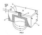
- FIG. 2A perspective view of one possible embodiment of a completed vertical capacitor, including electrical contacts 52 and 54 , is shown in FIG. 2 . In this example, active CMOS components 56 have been fabricated on the top surface of substrate 20 . For illustration purposes, isolation layer 40 and the lower portion of hole-filling metal 50 are not shown in FIG. 2 .
- the present methodis an all-dry process, thereby eliminating the possibility of liquid solution particulates clogging the through-substrate vias, as may happen when using prior art techniques.
- Wet processing techniquesmay be used in the final steps of the process in FIG. 1 to plug the via, since at this stage the via is isolated and electrically continuous across its length, and thus clogging due to solution particulates does not reduce via operability.
- the present ALD-based processprovides good control over layer thickness (typically, to within several nanometers), such that conformal coatings and high yields are reliably achieved. This also enables the fabrication of a very thin dielectric layer 46 , further increasing the potential capacitance of the device. Furthermore, the ability to deposit both insulators and metals using ALD provides a means of forming both isolation and conductive layers in a single process operation. Note, however, that the processing time needed for the present process may be considerably longer than that required by prior art methods, but the process is compatible with batch fabrication and automated operation. Employing ALD results in all surfaces being coated with the material layer being deposited; as such, it is necessary to pattern and etch the substrate to remove the deposited isolation and conductive material layers from areas where they are not needed. The present method enables high aspect ratio vertical capacitors to be fabricated in substrates having a thickness of greater than 50 ⁇ m. For best performance, the conductive material layers should have a high conductivity, and the isolation material layers should have a high dielectric breakdown strength.
- Additional techniquescan be employed to further increase the capacitance that can be achieved by the present method.
- extended etch patternscan be formed in the sidewalls of second cavity 32 , such that the cavity's surface area—and thereby the structure's capacitance—is increased.
- Another approachis to vary the shape of the structure; for example, the capacitor's two metal layers and intervening dielectric layer can be formed into a spiral shape or a meandering line, thereby providing more surface area and more capacitance.
- FIG. 3One possible example is shown in FIG. 3 .
- Fabrication of this vertical capacitor structurestarts with a two-sided etch: on the topside of a substrate 60 , a circular via 62 is etched, while on the backside, a central circular via 64 is etched, along with two concentric circular trenches 66 , 68 around it. The central vias meet and form a continuous via through the substrate.
- the etched substratethen goes through a first ALD deposition step in which the capacitor's first metal layer 70 is deposited, a second ALD deposition step in which the capacitor's dielectric layer 72 is depositied, and a third ALD deposition step in which the capacitor's second metal layer 74 is deposited.
- a hole-filling stepmight also be performed in which any remaining through-substrate via is filled with metal.
- the deposited layersare continuous over the surfaces, and bridge between the two backside trenches, going over the unetched (surface) portions of the substrate and coating the bottoms of the etched trenches.
- Contacts 76 and 78 to metal layers 70 and 74are provided to access the two terminals of the capacitor.
- additional backside etch trenchesadditional sidewall surface area is created, which creates additional capacitance.
- the present processis well-suited to use with a multi-layer stack of substrates, in which a substrate containing vertical capacitors as described herein is bonded together with a plurality of additional substrates.
- the bonding between substratesis effected with, for example, solder bumps, indium columns, Au—Au thermocompression bonding or glue.
- the bonding meansprovides a mechanical function, and can also provide an electrical function when the bonds effect electrical interconnections between individual substrate layers. Signals may be routed from one substrate to another through vias, as well as via the bonding means.
- embodiments of this inventioncan be combined with other circuit chips and systems.
- embodiments of the inventioncan be used for compact electronic circuits with multiple stacking layers and circuitry.
- Other usesinclude an enhanced three-dimensional electronic imager having wide dynamic range and pixel level image processing due to the density with which vertical capacitors can be fabricated on the wafer, RF filters, FPA ROICs, and 3D consumer electronics.
- Other applicationsinclude a vertically interconnected sensor array which provides signal processing in conjunction with infrared sensor systems, an arrayed acoustic sensing system, LADAR, and microprocessor circuits in which latency across the chip presents an issue.
- substrates having high aspect ratio through-substrate viasare intended to be used as standalone substrates or in combination with other types of substrates or systems.
- the foregoingis intended to cover all modifications and alternative constructions falling within the spirit and scope of the invention as expressed in the appended claims, wherein no portion of the disclosure is intended, expressly or implicitly, to be dedicated to the public domain if not set forth in the claims.
Landscapes
- Engineering & Computer Science (AREA)
- Power Engineering (AREA)
- Microelectronics & Electronic Packaging (AREA)
- Manufacturing & Machinery (AREA)
- Physics & Mathematics (AREA)
- Condensed Matter Physics & Semiconductors (AREA)
- General Physics & Mathematics (AREA)
- Computer Hardware Design (AREA)
- Semiconductor Integrated Circuits (AREA)
- Internal Circuitry In Semiconductor Integrated Circuit Devices (AREA)
Abstract
Description
- The invention was made with Government support promoted by the Defense Advanced Research Projects Office (DARPA), Microsystems Technology Office (MTO), under contract N00173-06-C-2055 awarded by the U.S. Department of the Navy, Office of Naval Research (ONR), Naval Research Laboratory (NRL), to Rockwell Collins, Inc. (RCI), and under purchase order 4502114317 awarded by RCI to Teledyne Scientific & Imaging, LLC. The Government has certain rights in the invention.
- This invention is directed to a method for fabricating vertical capacitors.
- The fabrication of integrated circuit (IC) chips has become a sophisticated process that can allow complex circuitry to be densely packaged onto a single substrate or wafer. Originally, most chips were fabricated in a simple planar design. However, planar chip designs limit the amount of circuitry that can be placed on a single substrate.
- To overcome some of the limitations resulting from the planar design, designers began stacking chips to form three-dimensional designs. Vias extending through the substrate—i.e., “through-substrate vias”—create three-dimensional interconnects which facilitate connection to the circuitry throughout the chip, thereby allowing the implementation of more advanced circuits and enabling a higher density of complex circuitry to be placed within a given die area. Furthermore, a three-dimensional design with through-substrate vias can enable advanced micro-electronic chip stacking, which can result, for example, in increased processing power for image data and signal processing.
- Another area that can be improved with 3D integration is capacitive circuit components. Planar RF filters and switched capacitor bank filters, for example, occupy significant die area; as such, integrated single-chip filters are often limited by die size, since the conventional metal-insulator-metal (MIM) capacitors used by such filters require substantial die area for large capacitance values. This can be overcome with the use of vertical capacitor structures, which are conventionally formed by adding additional insulating and conductive layers to a through-substrate via. Vertical capacitors enable substantial reductions in size to be achieved, with a direct correlation to reduced die cost. Such vertical capacitor structures provide advantages in readout circuits, for example, such as those for electronic imaging applications and active LIDAR. These circuits presently use planar capacitors for storage of photogenerated charge. For small pixel devices, the amount of charge storage capacity provided by conventional IC fabrication technology is limited by the physical constraints of pixel pitch. This limits the maximum achievable full well capacity, and can thus negatively impact important focal plane array characteristics, such as maximum intensity and dynamic range. Having the ability to significantly increase the capacitor value and/or the number of capacitors in a circuit, while preserving small die area, could relax these constraints and allow greater design flexibility and improved device performance.
- As noted above, one method of forming a vertical capacitor requires the fabrication of a through-substrate via. While a number of techniques are known for forming such vias, they are currently limited. In one approach, through-substrate vias have been formed in thick substrates—e.g., 200-400 μm; the thickness enables the substrates to retain mechanical durability and to be easily handled and processed without the need for sequential stacking and thinning operations. Using this approach, substrates are etched and the formed vias are electrically insulated and metallized. Although this approach provides some advantages, it introduces other limitations, such as the inability to fabricate small-diameter, fine-pitch vias. Indeed, using current etching techniques, the formation of high aspect ratio (i.e., ratio of depth to diameter) vias results in a large diameter-to-pitch (i.e., the center-to-center measurement between vias) ratio for the vias. This limits the etch depth of the vias, and also reduces the amount of available space on the substrate for other uses. Current techniques typically produce vias having diameters of about 4 μm with a depth of about 20 μm (using low temperature techniques) and 100 μm diameters with a depth of about 500 μm (using high temperature techniques); thus, an aspect ratio of about 5:1 is provided with either high or low temperature techniques. Both dry etching and wet etching have been demonstrated for the thick wafer processing, and both suffer from constraints on via size and separation. In addition, it is very difficult to reliably deposit electrical isolation material layers and metallic conductors using low process temperatures in high aspect ratio vias.
- To reduce via diameters, some techniques sequentially stack, bond and thin multiple wafers into a ‘single’ wafer stack and form the vias through only a single thin layer of the stacked wafers at a time, thereby reducing the aspect ratio and diameter required of an individual via. This approach involves wafer ‘thinning’, in which the wafers to be stacked are bonded and one portion (non-circuit containing, exposed surface) of the stacked wafers is thinned to reduce the wafer thickness, typically down to 10-25 μm. At this thickness, small diameter vias can be etched through the thinned layer while maintaining separation between neighboring vias. Alternatively, the via could be etched to a limited depth prior to the bonding, and then have its bottom (non-circuit containing) surface exposed in the thinning operation after bonding. This approach can use well-developed fabrication processes; however, disadvantages arise from the need for sequential processing of each successive layer and the complexity of intermediate testing. Further, the thinning of the stacked wafers reduces their integrity and makes them more susceptible to breakage during use and damage from handling. Further still, many current bonding techniques involve high temperatures, high voltage and/or high pressure, each of which poses difficulties if the stacking includes prefabricated integrated circuits with multi-level interconnects. Further, sequential circuit wafers can only be stacked in one orientation, with active circuitry at the bond interface, since the thinning process must only remove unprocessed substrate. Finally, the wafer-level sequential stacking can introduce stacked device yield impacts resulting from the random alignment of defects in a die from one layer with a good die in another, reducing operability at the stack level.
- In addition to a hole that passes completely through a substrate, a through-substrate via generally also requires an insulating layer lining the inner surfaces of the hole, and a conductive layer over the insulating layer. For a high aspect ratio via having a narrow diameter, it can be difficult to provide these insulating and conductive layers. One technique for forming such a via is described in co-pending patent application Ser. No. 11/167,014 to Borwick et al. and assigned to the present assignee. Here, wet processing is used to provide the via's sidewall seed layer and conductive layer. However, it can be difficult to achieve uniform seed layer coverage using wet processing, and particulates in the liquid solution can clog the vias, particularly those having a small diameter.
- A vertical capacitor fabrication method is presented which overcomes the problems noted above, providing high aspect ratio vertical capacitors with a process that eliminates difficulties associated with wet processing.
- The present fabrication method forms vertical capacitors in a substrate having first and second surfaces. The method is preferably an all-dry process, comprising:
- forming a through-substrate via hole in the substrate;
- depositing a first conductive material layer into the via hole using atomic layer deposition (ALD) such that the first conductive material layer is electrically continuous across the length of the via hole;
- depositing a first isolation material layer over the first conductive layer using ALD, the first isolation material layer being electrically insulating, continuous and substantially conformal; and
- depositing a second conductive material layer over the first isolation material layer using ALD such that the second conductive material layer is electrically continuous across the length of the via hole;
- such that the first and second conductive material layers and the first isolation material layer form a vertical capacitor.
- The through-substrate via hole is preferably formed by dry etching a first cavity having a first diameter into the substrate's first surface, and dry etching a second cavity having a second diameter into the substrate's second surface, such that the first and second cavities form a single continuous aperture through the substrate. The present method may be successfully practiced at temperatures of less than 200° C., thereby avoiding damage to circuitry residing on the substrate that might otherwise occur.
- These and other features, aspects, and advantages of the present invention will become better understood with reference to the following drawings, description, and claims.
- The detailed description of embodiments of the invention will be made with reference to the accompanying drawings, wherein like numerals designate corresponding parts in the figures.
FIGS. 1 a-1jare sectional views of a fabrication process for forming high aspect ratio vertical capacitors in accordance with the present invention.FIG. 2 is a perspective view of a vertical capacitor formed in accordance with the present fabrication process.FIG. 3 is a sectional view of another possible embodiment of a vertical capacitor formed in accordance with the present fabrication process, which includes an extended backside etch pattern.- The present method is directed to a process for fabricating high aspect ratio vertical capacitors. The basic process steps are illustrated in the series of sectional views shown in
FIGS. 1 a-1i. InFIG. 1 a, asubstrate 20 has afirst surface 22 and asecond surface 24. Circuitry (not shown) may be disposed onfirst surface 22, onsecond surface 24, and/or betweensurfaces - Fabricating a vertical capacitor per the present invention requires that a via first be formed through
substrate 20. The through-substrate via is preferably, though not necessarily, formed by etching first and second cavities having different diameters intosurfaces - In
FIG. 1 b, afirst cavity 30 is etched intofirst surface 22. The first cavity has a first diameter, and extends a first depth into the substrate. The first diameter is typically chosen to minimize the consumed circuit area onsurface 22, and the first depth is typically chosen to enable the first cavity to extend below the depth of any active circuitry onsurface 22. Then, as shown inFIG. 1 c, asecond cavity 32 having a second diameter, is etched coaxially withfirst cavity 30 intosecond surface 24. The second cavity is etched to a second depth such that it communicates withfirst cavity 30 to form a continuous aperture through the entire thickness of the substrate. The first and second cavities preferably extend to depths in the range of 20 μm-200 μm and 100 μm-350 μm, respectively, and have diameters of 2 μm-8 μm and 6 μm-25 μm, respectively. The larger diameter of the second cavity enables a greater depth to be achieved at the same aspect ratio. This enables the continuous aperture to extend through a greater total wafer thickness, while minimizing the circuit area onsurface 22 consumed by the via. - The cavities are preferably formed by dry etching, preferably using a deep reactive ion etching process (“DRIE”). A preferred DRIE process used for silicon etching known as the Bosch process utilizes time-sequenced alternating etch and passivation steps. An etchant such as sulfur hexafluoride SF6is used to etch a portion of the cavity into the substrate. To passivate the side wall of the cavity and prevent further lateral etching, an insulating layer is subsequently deposited using a separate gas composition which includes a species such as octafluorocyclobutane C4F8. This process is repeated until the desired depth is achieved. Etching via this process allows for high selectivity and achieves substantially vertical side walls, with aspect ratios as high as 40:1 or more. This high aspect ratio facilitates the production of smaller diameter cavities and smaller via-to-via spacings, as it reduces the amount of lateral blooming during etching and reduces side wall scalloping.
- A vertical capacitor is accordance with the present invention can be ‘floating’ relative to the substrate, in which the capacitor's metal layers are isolated from
substrate 20, or non-floating. If floating, the next step is to deposit anisolation material layer 40 as shown inFIG. 1 d. Here,isolation material layer 40 is deposited directly ontosubstrate 20 and onto the interior walls of the aperture so as to provide an isolation material layer that is electrically insulating, continuous and substantially conformal. The uniform coverage of the sidewalls withisolation material layer 40 acts to electrically isolate the through-substrate via from the substrate, as well as from other through-substrate vias being fabricated insubstrate 20.Isolation material layer 40 may be formed by any of several methods, including thermal oxidation, plasma enhanced chemical vapor deposition (PECVD) or chemical vapor deposition (CVD), or (ALD) - The isolation material layer preferably comprises inorganic oxides capable of providing electrical insulation and conformal surface coatings; metal oxides, including the oxides of aluminum, titanium, tantalum, niobium, zirconium, hafnium, lanthanum, yttrium, cerium, silicon, scandium, chromium, and erbium, are suitable.
- ALD is a gas phase chemical process used to create thin film coatings that are highly conformal and have extremely precise thickness control. The majority of ALD reactions use two chemicals, typically called precursors. These precursors react with a surface one-at-a-time in a sequential manner. By exposing the precursors to the growth surface repeatedly, a thin film is deposited. Additional details about ALD can be found, for example, in “Surface Chemistry for Atomic Layer Growth”, S. M. George et al.,Phys. Chem., Vol. 100, No. 31 (1996), pp. 13121-13131.
- After the isolation material layer40 (if used) has been deposited onto the substrate, an electrically
conductive material layer 44 is deposited over the isolation material layer using ALD such that the conductive material layer is electrically continuous across the length of the via hole; this is shown inFIG. 1 e. (If the capacitor is non-floating,conductive material layer 44 is deposited using ALD directly ontosubstrate 20 and onto the interior walls of the aperture, such thatlayer 44, and thus one terminal of the capacitor, are in contact withsubstrate 20 and therefore at ground potential). The conductive material layer is preferably chosen from a group consisting of nickel, palladium, platinum, ruthenium, tungsten, iridium, copper, molybdenum or zinc oxide. The dry etching and ALD deposition steps are preferably conducted at a temperature of less than 200° C., such that circuitry residing on the substrate, such as CMOS circuitry, is not damaged by excessive heat. - In some cases, it may be desirable to ‘activate’
isolation material layer 40 prior to the deposition ofconductive material layer 44, to make the isolation material layer more conducive to receiving the conductive material layer. This can be accomplished by depositing a seed layer (not shown) ontoisolation material layer 40; this is preferably accomplished using ALD, which deposits a conformal seed layer uniformly on the deep-etched sidewalls of the via. A seed layer is selected which will cause a reaction withconductive material layer 44 when the conductive material layer is deposited onto the substrate; palladium is one possible seed layer. Onceisolation material layer 40 is activated,conductive material layer 44 is deposited onto the activated isolation material layer. This seed layer, if conductive, may also reduce the series resistance of the final device. - Next, a thick insulating layer may be deposited over
conductive material layer 44, and then patterned and etched to provide insulatinglayer 45 as shown inFIG. 1 f.Layer 45 may be, for example, an oxide, nitride, or oxynitride layer, deposited by means of plasma enhanced chemical vapor deposition (PECVD). A completed vertical capacitor will includemetal layer 44 and a second metal layer deposited in a subsequent processing step.Layer 45 serves as an etch stop layer, to facilitate selective patterning of the second metal layer without exposingmetal layer 44. - An isolation material layer that will serve as the capacitor's dielectric layer is deposited next. In
FIG. 1 g, anisolation material layer 46 is deposited using ALD such that it is electrically insulating, continuous and substantially conformal. Theisolation material layer 46 is preferably made from a material which has a high dielectric constant, such as hafnium oxide (HfO2), in order to maximize the structure's capacitance for a given thickness oflayer 46. - To provide the capacitor's second metal layer, another electrically
conductive material layer 48 is deposited using ALD such that the conductive material layer is electrically continuous across the length of the via hole; this is shown inFIG. 1 h. The conductive material layer is preferably chosen from a group consisting of nickel, palladium, platinum, ruthenium, tungsten, iridium, copper or zinc oxide. - As above, it may be desirable to ‘activate’
isolation material layer 46 prior to the deposition ofconductive material layer 48, to make the isolation material layer more conducive to receiving the conductive material layer. This can be accomplished by depositing a seed layer (not shown) ontoisolation material layer 46, preferably using ALD. - Preferably, any portions of
cavities layers metal 50, as shown inFIG. 1 i. This hole filling is done for two reasons. First, processing of the substrate with the hole in it is difficult: photoresist material layers may get sucked into the hole by vacuum chucks, and air bubbles that get trapped in the hole tend to pop and degrade the cosmetics of the subsequent surface pattern. Second, theconductive material layer 48 deposited by ALD is typically very thin, and hence may have a relatively high resistance. The hole is preferably filled using a plating process—preferably, an electroless plating of a material layer like nickel, gold, or copper; uniform electroless plating is facilitated by the uniform depositions achieved using ALD. This reduces the resistance of the center conductor and physically plugs the hole to permit resist processing. Electrolytic plating may also be used. This hole filling can also be used in the case of non-circular cavity designs onsurface 24, reducing deep surface relief that can interfere with subsequent processing. - Additional processing may be performed to remove the isolation and conductive layers from areas where they are not needed, but leaving the completed vertical capacitor; one possible result is shown in
FIG. 1 j. Further, additional isolation material layers and conductive metal traces may be fabricated onsurfaces 22 and/or24 to route the electrical interconnection points to the desired locations on the surfaces. These process steps are not shown, and use fabrication techniques well known to those skilled in semiconductor processing. A perspective view of one possible embodiment of a completed vertical capacitor, includingelectrical contacts FIG. 2 . In this example,active CMOS components 56 have been fabricated on the top surface ofsubstrate 20. For illustration purposes,isolation layer 40 and the lower portion of hole-fillingmetal 50 are not shown inFIG. 2 . - With the possible exception of the hole-filling step, the present method is an all-dry process, thereby eliminating the possibility of liquid solution particulates clogging the through-substrate vias, as may happen when using prior art techniques. Wet processing techniques may be used in the final steps of the process in
FIG. 1 to plug the via, since at this stage the via is isolated and electrically continuous across its length, and thus clogging due to solution particulates does not reduce via operability. - The present ALD-based process provides good control over layer thickness (typically, to within several nanometers), such that conformal coatings and high yields are reliably achieved. This also enables the fabrication of a very thin
dielectric layer 46, further increasing the potential capacitance of the device. Furthermore, the ability to deposit both insulators and metals using ALD provides a means of forming both isolation and conductive layers in a single process operation. Note, however, that the processing time needed for the present process may be considerably longer than that required by prior art methods, but the process is compatible with batch fabrication and automated operation. Employing ALD results in all surfaces being coated with the material layer being deposited; as such, it is necessary to pattern and etch the substrate to remove the deposited isolation and conductive material layers from areas where they are not needed. The present method enables high aspect ratio vertical capacitors to be fabricated in substrates having a thickness of greater than 50 μm. For best performance, the conductive material layers should have a high conductivity, and the isolation material layers should have a high dielectric breakdown strength. - Additional techniques can be employed to further increase the capacitance that can be achieved by the present method. For example, extended etch patterns can be formed in the sidewalls of
second cavity 32, such that the cavity's surface area—and thereby the structure's capacitance—is increased. Another approach is to vary the shape of the structure; for example, the capacitor's two metal layers and intervening dielectric layer can be formed into a spiral shape or a meandering line, thereby providing more surface area and more capacitance. One possible example is shown inFIG. 3 . Fabrication of this vertical capacitor structure starts with a two-sided etch: on the topside of asubstrate 60, a circular via 62 is etched, while on the backside, a central circular via 64 is etched, along with two concentriccircular trenches - The etched substrate then goes through a first ALD deposition step in which the capacitor's
first metal layer 70 is deposited, a second ALD deposition step in which the capacitor'sdielectric layer 72 is depositied, and a third ALD deposition step in which the capacitor'ssecond metal layer 74 is deposited. A hole-filling step (not illustrated) might also be performed in which any remaining through-substrate via is filled with metal. The deposited layers are continuous over the surfaces, and bridge between the two backside trenches, going over the unetched (surface) portions of the substrate and coating the bottoms of the etched trenches.Contacts metal layers - The present process is well-suited to use with a multi-layer stack of substrates, in which a substrate containing vertical capacitors as described herein is bonded together with a plurality of additional substrates. The bonding between substrates is effected with, for example, solder bumps, indium columns, Au—Au thermocompression bonding or glue. The bonding means provides a mechanical function, and can also provide an electrical function when the bonds effect electrical interconnections between individual substrate layers. Signals may be routed from one substrate to another through vias, as well as via the bonding means.
- Although the foregoing described the invention with preferred embodiments, this is not intended to limit the invention. Indeed, embodiments of this invention can be combined with other circuit chips and systems. For instance, embodiments of the invention can be used for compact electronic circuits with multiple stacking layers and circuitry. Other uses include an enhanced three-dimensional electronic imager having wide dynamic range and pixel level image processing due to the density with which vertical capacitors can be fabricated on the wafer, RF filters, FPA ROICs, and 3D consumer electronics. Other applications include a vertically interconnected sensor array which provides signal processing in conjunction with infrared sensor systems, an arrayed acoustic sensing system, LADAR, and microprocessor circuits in which latency across the chip presents an issue.
- As seen from the foregoing, substrates having high aspect ratio through-substrate vias are intended to be used as standalone substrates or in combination with other types of substrates or systems. In this regard, the foregoing is intended to cover all modifications and alternative constructions falling within the spirit and scope of the invention as expressed in the appended claims, wherein no portion of the disclosure is intended, expressly or implicitly, to be dedicated to the public domain if not set forth in the claims.
Claims (44)
Priority Applications (1)
| Application Number | Priority Date | Filing Date | Title |
|---|---|---|---|
| US12/291,263US8088667B2 (en) | 2008-11-05 | 2008-11-05 | Method of fabricating vertical capacitors in through-substrate vias |
Applications Claiming Priority (1)
| Application Number | Priority Date | Filing Date | Title |
|---|---|---|---|
| US12/291,263US8088667B2 (en) | 2008-11-05 | 2008-11-05 | Method of fabricating vertical capacitors in through-substrate vias |
Publications (2)
| Publication Number | Publication Date |
|---|---|
| US20100110607A1true US20100110607A1 (en) | 2010-05-06 |
| US8088667B2 US8088667B2 (en) | 2012-01-03 |
Family
ID=42131094
Family Applications (1)
| Application Number | Title | Priority Date | Filing Date |
|---|---|---|---|
| US12/291,263Expired - Fee RelatedUS8088667B2 (en) | 2008-11-05 | 2008-11-05 | Method of fabricating vertical capacitors in through-substrate vias |
Country Status (1)
| Country | Link |
|---|---|
| US (1) | US8088667B2 (en) |
Cited By (13)
| Publication number | Priority date | Publication date | Assignee | Title |
|---|---|---|---|---|
| US20100127346A1 (en)* | 2008-11-21 | 2010-05-27 | Denatale Jeffrey F | Power distribution for cmos circuits using in-substrate decoupling capacitors and back side metal layers |
| US20100264548A1 (en)* | 2009-04-16 | 2010-10-21 | Freescale Semiconductor, Inc. | Through substrate vias |
| US20100308435A1 (en)* | 2009-06-08 | 2010-12-09 | Qualcomm Incorporated | Through Silicon Via With Embedded Decoupling Capacitor |
| US20120075817A1 (en)* | 2009-03-09 | 2012-03-29 | Yeates Kyle H | Multi-part substrate assemblies for low profile portable electronic devices |
| CN102623173A (en)* | 2012-04-17 | 2012-08-01 | 电子科技大学 | A method for preparing capacitors based on alumina ordered nanopore structure |
| CN103311221A (en)* | 2012-12-25 | 2013-09-18 | 财团法人交大思源基金会 | Semiconductor device integrated with passive element |
| US20150198775A1 (en)* | 2012-08-31 | 2015-07-16 | Gurtej Sandhu | Method of forming photonics structures |
| EP3128743A4 (en)* | 2014-03-31 | 2017-12-20 | Nikon Corporation | Detection element, lock-in detection device, substrate, and manufacturing method for detection element |
| US20190140167A1 (en)* | 2017-11-07 | 2019-05-09 | Everspin Technologies, Inc. | Angled surface removal process and structure relating thereto |
| CN110637359A (en)* | 2018-03-06 | 2019-12-31 | 株式会社东芝 | Capacitor and its manufacturing method |
| US20200105646A1 (en)* | 2018-10-01 | 2020-04-02 | Nanya Technology Corporation | Semiconductor structure having through silicon via structure and method for forming the same |
| US11239384B2 (en)* | 2016-11-11 | 2022-02-01 | Infineon Technologiesag | Semiconductor wafers and semiconductor devices with barrier layer and methods of manufacturing |
| US11557550B2 (en)* | 2018-01-25 | 2023-01-17 | Commissariat A L'energie Atomique Et Aux Energies Alternatives | Electronic chip, the rear face of which is protected by an improved embrittlement structure |
Families Citing this family (3)
| Publication number | Priority date | Publication date | Assignee | Title |
|---|---|---|---|---|
| JP5275401B2 (en)* | 2011-04-18 | 2013-08-28 | 新光電気工業株式会社 | WIRING BOARD, SEMICONDUCTOR DEVICE, AND WIRING BOARD MANUFACTURING METHOD |
| US9196671B2 (en) | 2012-11-02 | 2015-11-24 | International Business Machines Corporation | Integrated decoupling capacitor utilizing through-silicon via |
| US9496326B1 (en) | 2015-10-16 | 2016-11-15 | International Business Machines Corporation | High-density integrated circuit via capacitor |
Citations (10)
| Publication number | Priority date | Publication date | Assignee | Title |
|---|---|---|---|---|
| US5421083A (en)* | 1994-04-01 | 1995-06-06 | Motorola, Inc. | Method of manufacturing a circuit carrying substrate having coaxial via holes |
| US6278181B1 (en)* | 1999-06-28 | 2001-08-21 | Advanced Micro Devices, Inc. | Stacked multi-chip modules using C4 interconnect technology having improved thermal management |
| US6565730B2 (en)* | 1999-12-29 | 2003-05-20 | Intel Corporation | Self-aligned coaxial via capacitors |
| US6717071B2 (en)* | 2000-08-11 | 2004-04-06 | Industrial Technology Research Institute | Coaxial via hole and process of fabricating the same |
| US6852627B2 (en)* | 2003-03-05 | 2005-02-08 | Micron Technology, Inc. | Conductive through wafer vias |
| US6960479B2 (en)* | 2001-07-20 | 2005-11-01 | Intel Corporation | Stacked ferroelectric memory device and method of making same |
| US6968110B2 (en)* | 2003-04-21 | 2005-11-22 | Sioptical, Inc. | CMOS-compatible integration of silicon-based optical devices with electronic devices |
| US6984561B2 (en)* | 2002-12-19 | 2006-01-10 | Matrix Semiconductor, Inc. | Method for making high density nonvolatile memory |
| US6995072B2 (en)* | 1998-01-23 | 2006-02-07 | Micron Technology, Inc. | Method of making sacrificial self-aligned interconnection structure |
| US20100001378A1 (en)* | 2008-07-01 | 2010-01-07 | Teledyne Scientific & Imaging, Llc | Through-substrate vias and method of fabricating same |
Family Cites Families (19)
| Publication number | Priority date | Publication date | Assignee | Title |
|---|---|---|---|---|
| IL67556A (en) | 1981-12-28 | 1987-10-20 | Chevron Res | Batteries fabricated with electroactive polymers |
| US4855017A (en) | 1985-05-03 | 1989-08-08 | Texas Instruments Incorporated | Trench etch process for a single-wafer RIE dry etch reactor |
| US4961821A (en) | 1989-11-22 | 1990-10-09 | Xerox Corporation | Ode through holes and butt edges without edge dicing |
| DE4241045C1 (en) | 1992-12-05 | 1994-05-26 | Bosch Gmbh Robert | Process for anisotropic etching of silicon |
| FR2767223B1 (en) | 1997-08-06 | 1999-09-17 | Commissariat Energie Atomique | INTERCONNECTION METHOD THROUGH SEMICONDUCTOR MATERIAL, AND DEVICE OBTAINED |
| EP0926723B1 (en) | 1997-11-26 | 2007-01-17 | STMicroelectronics S.r.l. | Process for forming front-back through contacts in micro-integrated electronic devices |
| US6458615B1 (en) | 1999-09-30 | 2002-10-01 | Carnegie Mellon University | Method of fabricating micromachined structures and devices formed therefrom |
| US6446317B1 (en) | 2000-03-31 | 2002-09-10 | Intel Corporation | Hybrid capacitor and method of fabrication therefor |
| US6605551B2 (en) | 2000-12-08 | 2003-08-12 | Intel Corporation | Electrocoating process to form a dielectric layer in an organic substrate to reduce loop inductance |
| JP3834589B2 (en) | 2001-06-27 | 2006-10-18 | 株式会社ルネサステクノロジ | Manufacturing method of semiconductor device |
| US20030104649A1 (en) | 2001-08-15 | 2003-06-05 | Mehmet Ozgur | Method for making CMOS-based monolithic micro electromechanical system (MEMS) integrated circuits and integrated circuits made thereby |
| US6716737B2 (en) | 2002-07-29 | 2004-04-06 | Hewlett-Packard Development Company, L.P. | Method of forming a through-substrate interconnect |
| US7091424B2 (en) | 2002-10-10 | 2006-08-15 | International Business Machines Corporation | Coaxial via structure for optimizing signal transmission in multiple layer electronic device carriers |
| JP4056854B2 (en) | 2002-11-05 | 2008-03-05 | 新光電気工業株式会社 | Manufacturing method of semiconductor device |
| US7026184B2 (en) | 2003-02-26 | 2006-04-11 | Carnegie Mellon University | Method of fabricating microstructures and devices made therefrom |
| DE10345460B4 (en) | 2003-09-30 | 2007-01-04 | Infineon Technologies Ag | A method of making a hole trench storage capacitor in a semiconductor substrate |
| US6955962B2 (en) | 2003-10-31 | 2005-10-18 | Infineon Technologies Richmond, Lp | Deep trench capacitor having increased surface area |
| US7618837B2 (en) | 2004-06-29 | 2009-11-17 | Peking University | Method for fabricating high aspect ratio MEMS device with integrated circuit on the same substrate using post-CMOS process |
| US20060003566A1 (en) | 2004-06-30 | 2006-01-05 | Ismail Emesh | Methods and apparatuses for semiconductor fabrication utilizing through-wafer interconnects |
- 2008
- 2008-11-05USUS12/291,263patent/US8088667B2/ennot_activeExpired - Fee Related
Patent Citations (11)
| Publication number | Priority date | Publication date | Assignee | Title |
|---|---|---|---|---|
| US5421083A (en)* | 1994-04-01 | 1995-06-06 | Motorola, Inc. | Method of manufacturing a circuit carrying substrate having coaxial via holes |
| US6995072B2 (en)* | 1998-01-23 | 2006-02-07 | Micron Technology, Inc. | Method of making sacrificial self-aligned interconnection structure |
| US6278181B1 (en)* | 1999-06-28 | 2001-08-21 | Advanced Micro Devices, Inc. | Stacked multi-chip modules using C4 interconnect technology having improved thermal management |
| US6565730B2 (en)* | 1999-12-29 | 2003-05-20 | Intel Corporation | Self-aligned coaxial via capacitors |
| US6963483B2 (en)* | 1999-12-29 | 2005-11-08 | Intel Corporation | Self-aligned coaxial via capacitors |
| US6717071B2 (en)* | 2000-08-11 | 2004-04-06 | Industrial Technology Research Institute | Coaxial via hole and process of fabricating the same |
| US6960479B2 (en)* | 2001-07-20 | 2005-11-01 | Intel Corporation | Stacked ferroelectric memory device and method of making same |
| US6984561B2 (en)* | 2002-12-19 | 2006-01-10 | Matrix Semiconductor, Inc. | Method for making high density nonvolatile memory |
| US6852627B2 (en)* | 2003-03-05 | 2005-02-08 | Micron Technology, Inc. | Conductive through wafer vias |
| US6968110B2 (en)* | 2003-04-21 | 2005-11-22 | Sioptical, Inc. | CMOS-compatible integration of silicon-based optical devices with electronic devices |
| US20100001378A1 (en)* | 2008-07-01 | 2010-01-07 | Teledyne Scientific & Imaging, Llc | Through-substrate vias and method of fabricating same |
Cited By (29)
| Publication number | Priority date | Publication date | Assignee | Title |
|---|---|---|---|---|
| US20100127346A1 (en)* | 2008-11-21 | 2010-05-27 | Denatale Jeffrey F | Power distribution for cmos circuits using in-substrate decoupling capacitors and back side metal layers |
| US7906404B2 (en)* | 2008-11-21 | 2011-03-15 | Teledyne Scientific & Imaging, Llc | Power distribution for CMOS circuits using in-substrate decoupling capacitors and back side metal layers |
| US20120075817A1 (en)* | 2009-03-09 | 2012-03-29 | Yeates Kyle H | Multi-part substrate assemblies for low profile portable electronic devices |
| US8879272B2 (en)* | 2009-03-09 | 2014-11-04 | Apple Inc. | Multi-part substrate assemblies for low profile portable electronic devices |
| US8329579B2 (en) | 2009-04-16 | 2012-12-11 | Freescale Semiconductor, Inc. | Through substrate VIAS |
| US8062975B2 (en)* | 2009-04-16 | 2011-11-22 | Freescale Semiconductor, Inc. | Through substrate vias |
| US20100264548A1 (en)* | 2009-04-16 | 2010-10-21 | Freescale Semiconductor, Inc. | Through substrate vias |
| US20100308435A1 (en)* | 2009-06-08 | 2010-12-09 | Qualcomm Incorporated | Through Silicon Via With Embedded Decoupling Capacitor |
| US8536678B2 (en) | 2009-06-08 | 2013-09-17 | Qualcomm Incorporated | Through substrate via with embedded decoupling capacitor |
| US8294240B2 (en)* | 2009-06-08 | 2012-10-23 | Qualcomm Incorporated | Through silicon via with embedded decoupling capacitor |
| CN102623173A (en)* | 2012-04-17 | 2012-08-01 | 电子科技大学 | A method for preparing capacitors based on alumina ordered nanopore structure |
| US10761275B2 (en) | 2012-08-31 | 2020-09-01 | Micron Technology, Inc. | Method of forming photonics structures |
| US20150198775A1 (en)* | 2012-08-31 | 2015-07-16 | Gurtej Sandhu | Method of forming photonics structures |
| US12326599B2 (en) | 2012-08-31 | 2025-06-10 | Micron Technology, Inc. | Method of forming photonics structures |
| US10094988B2 (en)* | 2012-08-31 | 2018-10-09 | Micron Technology, Inc. | Method of forming photonics structures |
| US11886019B2 (en) | 2012-08-31 | 2024-01-30 | Micron Technology, Inc. | Method of forming photonics structures |
| US11402590B2 (en) | 2012-08-31 | 2022-08-02 | Micron Technology, Inc. | Method of forming photonics structures |
| CN103311221A (en)* | 2012-12-25 | 2013-09-18 | 财团法人交大思源基金会 | Semiconductor device integrated with passive element |
| TWI488286B (en)* | 2012-12-25 | 2015-06-11 | Univ Nat Chiao Tung | Semiconductor device integrating passive components |
| EP3128743A4 (en)* | 2014-03-31 | 2017-12-20 | Nikon Corporation | Detection element, lock-in detection device, substrate, and manufacturing method for detection element |
| US10026768B2 (en) | 2014-03-31 | 2018-07-17 | Nikon Corporation | Detector, detector with lock-in amplifier, substrate, and method for manufacturing a detector |
| US11239384B2 (en)* | 2016-11-11 | 2022-02-01 | Infineon Technologiesag | Semiconductor wafers and semiconductor devices with barrier layer and methods of manufacturing |
| US20190140167A1 (en)* | 2017-11-07 | 2019-05-09 | Everspin Technologies, Inc. | Angled surface removal process and structure relating thereto |
| US11557550B2 (en)* | 2018-01-25 | 2023-01-17 | Commissariat A L'energie Atomique Et Aux Energies Alternatives | Electronic chip, the rear face of which is protected by an improved embrittlement structure |
| EP3764394A4 (en)* | 2018-03-06 | 2022-02-23 | Kabushiki Kaisha Toshiba | CONDENSER AND METHOD OF MANUFACTURE THEREOF |
| CN110637359A (en)* | 2018-03-06 | 2019-12-31 | 株式会社东芝 | Capacitor and its manufacturing method |
| US11508525B2 (en) | 2018-03-06 | 2022-11-22 | Kabushiki Kaisha Toshiba | Capacitor having trenches on both surfaces |
| US20200105646A1 (en)* | 2018-10-01 | 2020-04-02 | Nanya Technology Corporation | Semiconductor structure having through silicon via structure and method for forming the same |
| TWI715890B (en)* | 2018-10-01 | 2021-01-11 | 南亞科技股份有限公司 | Semiconductor structure having through silicon via structure and method for preparing the same |
Also Published As
| Publication number | Publication date |
|---|---|
| US8088667B2 (en) | 2012-01-03 |
Similar Documents
| Publication | Publication Date | Title |
|---|---|---|
| US8088667B2 (en) | Method of fabricating vertical capacitors in through-substrate vias | |
| US7906404B2 (en) | Power distribution for CMOS circuits using in-substrate decoupling capacitors and back side metal layers | |
| US20100001378A1 (en) | Through-substrate vias and method of fabricating same | |
| US8187972B2 (en) | Through-substrate vias with polymer fill and method of fabricating same | |
| US7538032B2 (en) | Low temperature method for fabricating high-aspect ratio vias and devices fabricated by said method | |
| US7915710B2 (en) | Method of fabricating a semiconductor device, and semiconductor device with a conductive member extending through a substrate and connected to a metal pattern bonded to the substrate | |
| US6444576B1 (en) | Three dimensional IC package module | |
| JP5330376B2 (en) | Integrated device, method of manufacturing the same, and system-in-package | |
| CN101483149B (en) | A kind of preparation method of through-silicon via interconnection structure | |
| CN105097736B (en) | Utilize chip structure on wafer on the 3D substrate of rear via process | |
| US8633589B2 (en) | Dielectric trenches, nickel/tantalum oxide structures, and chemical mechanical polishing techniques | |
| US8034704B2 (en) | Method for manufacturing semiconductor device and semiconductor device | |
| US9123789B2 (en) | Chip with through silicon via electrode and method of forming the same | |
| US20100178747A1 (en) | Minimum Cost Method for Forming High Density Passive Capacitors for Replacement of Discrete Board Capacitors Using a Minimum Cost 3D Wafer-to-Wafer Modular Integration Scheme | |
| US20080122031A1 (en) | Vertical electrical device | |
| US20050248002A1 (en) | Fill for large volume vias | |
| JP2008172223A (en) | Method for manufacturing silicon carrier equipped with conductive through-via with low stress and low defect density, and semiconductor device having the carrier | |
| CN102420210A (en) | Device with through-silicon via (tsv) and method of forming the same | |
| US20100171218A1 (en) | Semiconductor device and method for fabricating the same | |
| JP2007043154A (en) | Method of manufacturing semiconductor structure having wafer through-contact and corresponding semiconductor structure | |
| US20080061443A1 (en) | Method of manufacturing semiconductor device | |
| US20210020737A1 (en) | Capacitor and method for producing the same | |
| CN101989621B (en) | Metal-insulator-metal (MIM) capacitor and manufacturing method thereof | |
| US20020085336A1 (en) | High performance via capacitor and method for manufacturing same | |
| US10147548B2 (en) | Capacitors using porous alumina structures |
Legal Events
| Date | Code | Title | Description |
|---|---|---|---|
| AS | Assignment | Owner name:TELEDYNE SCIENTIFIC & IMAGING, LLC,CALIFORNIA Free format text:ASSIGNMENT OF ASSIGNORS INTEREST;ASSIGNORS:DENATALE, JEFFREY F.;STUPAR, PHILIP A.;PAPAVASILIOU, ALEXANDROS P.;AND OTHERS;REEL/FRAME:021868/0695 Effective date:20081101 Owner name:TELEDYNE SCIENTIFIC & IMAGING, LLC, CALIFORNIA Free format text:ASSIGNMENT OF ASSIGNORS INTEREST;ASSIGNORS:DENATALE, JEFFREY F.;STUPAR, PHILIP A.;PAPAVASILIOU, ALEXANDROS P.;AND OTHERS;REEL/FRAME:021868/0695 Effective date:20081101 | |
| ZAAA | Notice of allowance and fees due | Free format text:ORIGINAL CODE: NOA | |
| ZAAB | Notice of allowance mailed | Free format text:ORIGINAL CODE: MN/=. | |
| STCF | Information on status: patent grant | Free format text:PATENTED CASE | |
| FEPP | Fee payment procedure | Free format text:PAYOR NUMBER ASSIGNED (ORIGINAL EVENT CODE: ASPN); ENTITY STATUS OF PATENT OWNER: LARGE ENTITY | |
| FPAY | Fee payment | Year of fee payment:4 | |
| MAFP | Maintenance fee payment | Free format text:PAYMENT OF MAINTENANCE FEE, 8TH YEAR, LARGE ENTITY (ORIGINAL EVENT CODE: M1552); ENTITY STATUS OF PATENT OWNER: LARGE ENTITY Year of fee payment:8 | |
| FEPP | Fee payment procedure | Free format text:MAINTENANCE FEE REMINDER MAILED (ORIGINAL EVENT CODE: REM.); ENTITY STATUS OF PATENT OWNER: LARGE ENTITY | |
| LAPS | Lapse for failure to pay maintenance fees | Free format text:PATENT EXPIRED FOR FAILURE TO PAY MAINTENANCE FEES (ORIGINAL EVENT CODE: EXP.); ENTITY STATUS OF PATENT OWNER: LARGE ENTITY | |
| STCH | Information on status: patent discontinuation | Free format text:PATENT EXPIRED DUE TO NONPAYMENT OF MAINTENANCE FEES UNDER 37 CFR 1.362 | |
| FP | Lapsed due to failure to pay maintenance fee | Effective date:20240103 |