US20100110434A1 - Alignment for Edge Field Nano-Imprinting - Google Patents
Alignment for Edge Field Nano-ImprintingDownload PDFInfo
- Publication number
- US20100110434A1 US20100110434A1US12/606,274US60627409AUS2010110434A1US 20100110434 A1US20100110434 A1US 20100110434A1US 60627409 AUS60627409 AUS 60627409AUS 2010110434 A1US2010110434 A1US 2010110434A1
- Authority
- US
- United States
- Prior art keywords
- alignment
- field
- alignment marks
- substrate
- sub
- Prior art date
- Legal status (The legal status is an assumption and is not a legal conclusion. Google has not performed a legal analysis and makes no representation as to the accuracy of the status listed.)
- Granted
Links
- 239000000758substrateSubstances0.000claimsabstractdescription73
- 238000000034methodMethods0.000claimsabstractdescription38
- 238000005259measurementMethods0.000claimsdescription32
- 238000004891communicationMethods0.000claimsdescription12
- 230000003287optical effectEffects0.000claimsdescription12
- 238000001459lithographyMethods0.000claimsdescription10
- 239000000463materialSubstances0.000description15
- 238000004519manufacturing processMethods0.000description8
- 238000000059patterningMethods0.000description7
- 238000001514detection methodMethods0.000description5
- 230000015572biosynthetic processEffects0.000description4
- 239000012530fluidSubstances0.000description3
- 239000007788liquidSubstances0.000description3
- VYPSYNLAJGMNEJ-UHFFFAOYSA-NSilicium dioxideChemical compoundO=[Si]=OVYPSYNLAJGMNEJ-UHFFFAOYSA-N0.000description2
- 238000005229chemical vapour depositionMethods0.000description2
- 238000013461designMethods0.000description2
- 238000005240physical vapour depositionMethods0.000description2
- 238000012545processingMethods0.000description2
- 238000007711solidificationMethods0.000description2
- 230000008023solidificationEffects0.000description2
- 238000012546transferMethods0.000description2
- 239000005388borosilicate glassSubstances0.000description1
- -1but not limited toSubstances0.000description1
- 238000000151depositionMethods0.000description1
- 230000008021depositionEffects0.000description1
- 238000011161developmentMethods0.000description1
- 238000003618dip coatingMethods0.000description1
- KPUWHANPEXNPJT-UHFFFAOYSA-NdisiloxaneChemical class[SiH3]O[SiH3]KPUWHANPEXNPJT-UHFFFAOYSA-N0.000description1
- 238000005516engineering processMethods0.000description1
- 239000010408filmSubstances0.000description1
- 229920002313fluoropolymerPolymers0.000description1
- 239000005350fused silica glassSubstances0.000description1
- 239000002184metalSubstances0.000description1
- 238000001000micrographMethods0.000description1
- 239000000203mixtureSubstances0.000description1
- 239000000178monomerSubstances0.000description1
- 229920000620organic polymerPolymers0.000description1
- 239000002245particleSubstances0.000description1
- 229920000642polymerPolymers0.000description1
- 238000004886process controlMethods0.000description1
- 239000010453quartzSubstances0.000description1
- 230000005855radiationEffects0.000description1
- 230000001105regulatory effectEffects0.000description1
- 229910052594sapphireInorganic materials0.000description1
- 239000010980sapphireSubstances0.000description1
- 239000004065semiconductorSubstances0.000description1
- 229910052710siliconInorganic materials0.000description1
- 239000010703siliconSubstances0.000description1
- 238000004528spin coatingMethods0.000description1
- 238000000427thin-film depositionMethods0.000description1
Images


Classifications
- G—PHYSICS
- G03—PHOTOGRAPHY; CINEMATOGRAPHY; ANALOGOUS TECHNIQUES USING WAVES OTHER THAN OPTICAL WAVES; ELECTROGRAPHY; HOLOGRAPHY
- G03F—PHOTOMECHANICAL PRODUCTION OF TEXTURED OR PATTERNED SURFACES, e.g. FOR PRINTING, FOR PROCESSING OF SEMICONDUCTOR DEVICES; MATERIALS THEREFOR; ORIGINALS THEREFOR; APPARATUS SPECIALLY ADAPTED THEREFOR
- G03F9/00—Registration or positioning of originals, masks, frames, photographic sheets or textured or patterned surfaces, e.g. automatically
- G—PHYSICS
- G03—PHOTOGRAPHY; CINEMATOGRAPHY; ANALOGOUS TECHNIQUES USING WAVES OTHER THAN OPTICAL WAVES; ELECTROGRAPHY; HOLOGRAPHY
- G03F—PHOTOMECHANICAL PRODUCTION OF TEXTURED OR PATTERNED SURFACES, e.g. FOR PRINTING, FOR PROCESSING OF SEMICONDUCTOR DEVICES; MATERIALS THEREFOR; ORIGINALS THEREFOR; APPARATUS SPECIALLY ADAPTED THEREFOR
- G03F7/00—Photomechanical, e.g. photolithographic, production of textured or patterned surfaces, e.g. printing surfaces; Materials therefor, e.g. comprising photoresists; Apparatus specially adapted therefor
- G03F7/0002—Lithographic processes using patterning methods other than those involving the exposure to radiation, e.g. by stamping
- B—PERFORMING OPERATIONS; TRANSPORTING
- B29—WORKING OF PLASTICS; WORKING OF SUBSTANCES IN A PLASTIC STATE IN GENERAL
- B29C—SHAPING OR JOINING OF PLASTICS; SHAPING OF MATERIAL IN A PLASTIC STATE, NOT OTHERWISE PROVIDED FOR; AFTER-TREATMENT OF THE SHAPED PRODUCTS, e.g. REPAIRING
- B29C33/00—Moulds or cores; Details thereof or accessories therefor
- B29C33/42—Moulds or cores; Details thereof or accessories therefor characterised by the shape of the moulding surface, e.g. ribs or grooves
- B—PERFORMING OPERATIONS; TRANSPORTING
- B82—NANOTECHNOLOGY
- B82Y—SPECIFIC USES OR APPLICATIONS OF NANOSTRUCTURES; MEASUREMENT OR ANALYSIS OF NANOSTRUCTURES; MANUFACTURE OR TREATMENT OF NANOSTRUCTURES
- B82Y10/00—Nanotechnology for information processing, storage or transmission, e.g. quantum computing or single electron logic
- B—PERFORMING OPERATIONS; TRANSPORTING
- B82—NANOTECHNOLOGY
- B82Y—SPECIFIC USES OR APPLICATIONS OF NANOSTRUCTURES; MEASUREMENT OR ANALYSIS OF NANOSTRUCTURES; MANUFACTURE OR TREATMENT OF NANOSTRUCTURES
- B82Y40/00—Manufacture or treatment of nanostructures
- G—PHYSICS
- G03—PHOTOGRAPHY; CINEMATOGRAPHY; ANALOGOUS TECHNIQUES USING WAVES OTHER THAN OPTICAL WAVES; ELECTROGRAPHY; HOLOGRAPHY
- G03F—PHOTOMECHANICAL PRODUCTION OF TEXTURED OR PATTERNED SURFACES, e.g. FOR PRINTING, FOR PROCESSING OF SEMICONDUCTOR DEVICES; MATERIALS THEREFOR; ORIGINALS THEREFOR; APPARATUS SPECIALLY ADAPTED THEREFOR
- G03F9/00—Registration or positioning of originals, masks, frames, photographic sheets or textured or patterned surfaces, e.g. automatically
- G03F9/70—Registration or positioning of originals, masks, frames, photographic sheets or textured or patterned surfaces, e.g. automatically for microlithography
- G03F9/7003—Alignment type or strategy, e.g. leveling, global alignment
- G03F9/7042—Alignment for lithographic apparatus using patterning methods other than those involving the exposure to radiation, e.g. by stamping or imprinting
- G—PHYSICS
- G03—PHOTOGRAPHY; CINEMATOGRAPHY; ANALOGOUS TECHNIQUES USING WAVES OTHER THAN OPTICAL WAVES; ELECTROGRAPHY; HOLOGRAPHY
- G03F—PHOTOMECHANICAL PRODUCTION OF TEXTURED OR PATTERNED SURFACES, e.g. FOR PRINTING, FOR PROCESSING OF SEMICONDUCTOR DEVICES; MATERIALS THEREFOR; ORIGINALS THEREFOR; APPARATUS SPECIALLY ADAPTED THEREFOR
- G03F9/00—Registration or positioning of originals, masks, frames, photographic sheets or textured or patterned surfaces, e.g. automatically
- G03F9/70—Registration or positioning of originals, masks, frames, photographic sheets or textured or patterned surfaces, e.g. automatically for microlithography
- G03F9/7003—Alignment type or strategy, e.g. leveling, global alignment
- G03F9/7046—Strategy, e.g. mark, sensor or wavelength selection
- G—PHYSICS
- G03—PHOTOGRAPHY; CINEMATOGRAPHY; ANALOGOUS TECHNIQUES USING WAVES OTHER THAN OPTICAL WAVES; ELECTROGRAPHY; HOLOGRAPHY
- G03F—PHOTOMECHANICAL PRODUCTION OF TEXTURED OR PATTERNED SURFACES, e.g. FOR PRINTING, FOR PROCESSING OF SEMICONDUCTOR DEVICES; MATERIALS THEREFOR; ORIGINALS THEREFOR; APPARATUS SPECIALLY ADAPTED THEREFOR
- G03F9/00—Registration or positioning of originals, masks, frames, photographic sheets or textured or patterned surfaces, e.g. automatically
- G03F9/70—Registration or positioning of originals, masks, frames, photographic sheets or textured or patterned surfaces, e.g. automatically for microlithography
- G03F9/7073—Alignment marks and their environment
- G03F9/7084—Position of mark on substrate, i.e. position in (x, y, z) of mark, e.g. buried or resist covered mark, mark on rearside, at the substrate edge, in the circuit area, latent image mark, marks in plural levels
- G—PHYSICS
- G03—PHOTOGRAPHY; CINEMATOGRAPHY; ANALOGOUS TECHNIQUES USING WAVES OTHER THAN OPTICAL WAVES; ELECTROGRAPHY; HOLOGRAPHY
- G03F—PHOTOMECHANICAL PRODUCTION OF TEXTURED OR PATTERNED SURFACES, e.g. FOR PRINTING, FOR PROCESSING OF SEMICONDUCTOR DEVICES; MATERIALS THEREFOR; ORIGINALS THEREFOR; APPARATUS SPECIALLY ADAPTED THEREFOR
- G03F9/00—Registration or positioning of originals, masks, frames, photographic sheets or textured or patterned surfaces, e.g. automatically
- G03F9/70—Registration or positioning of originals, masks, frames, photographic sheets or textured or patterned surfaces, e.g. automatically for microlithography
- G03F9/7088—Alignment mark detection, e.g. TTR, TTL, off-axis detection, array detector, video detection
Definitions
- Nano-fabricationincludes the fabrication of very small structures that have features on the order of 100 nanometers or smaller.
- One application in which nano-fabrication has had a sizeable impactis in the processing of integrated circuits.
- the semiconductor processing industrycontinues to strive for larger production yields while increasing the circuits per unit area formed on a substrate, therefore nano-fabrication becomes increasingly important.
- Nano-fabricationprovides greater process control while allowing continued reduction of the minimum feature dimensions of the structures formed.
- Other areas of development in which nano-fabrication has been employedinclude biotechnology, optical technology, mechanical systems, and the like.
- imprint lithographyAn exemplary nano-fabrication technique in use today is commonly referred to as imprint lithography.
- Exemplary imprint lithography processesare described in detail in numerous publications, such as U.S. Patent Publication No. 2004/0065976, U.S. Patent Publication No. 2004/0065252, and U.S. Pat. No. 6,936,194, all of which are hereby incorporated by reference.
- An imprint lithography technique disclosed in each of the aforementioned U.S. patent publications and patentincludes formation of a relief pattern in a formable layer (polymerizable) and transferring a pattern corresponding to the relief pattern into an underlying substrate.
- the substratemay be coupled to a motion stage to obtain a desired positioning to facilitate the patterning process.
- the patterning processuses a template spaced apart from the substrate and a formable liquid applied between the template and the substrate.
- the formable liquidis solidified to form a rigid layer that has a pattern conforming to a shape of the surface of the template that contacts the formable liquid.
- the templateis separated from the rigid layer such that the template and the substrate are spaced apart.
- the substrate and the solidified layerare then subjected to additional processes to transfer a relief image into the substrate that corresponds to the pattern in the solidified layer.
- FIG. 1illustrates a simplified side view of a lithographic system in accordance with an embodiment of the present invention.
- FIG. 2illustrates a simplified side view of the substrate shown in FIG. 1 having a patterned layer positioned thereon.
- FIG. 3illustrates a simplified top down view of an alignment system having multiple alignment measurement units about a field.
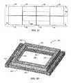
- FIG. 4illustrates a simplified top down view of a substrate.
- FIGS. 5A-5Eillustrate exemplary reconfigurable alignment systems.
- FIG. 6illustrates a flow chart of an exemplary method for aligning a template and a substrate.
- FIG. 7illustrates a simplified top down view of a portion of a substrate.
- FIG. 8illustrates a flow chart of an exemplary method for aligning a template and a substrate.
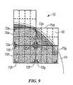
- FIG. 9illustrates a simplified top down view of a portion of a substrate.
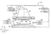
- a lithographic system 10used to form a relief pattern on substrate 12 .
- Substrate 12may be coupled to substrate chuck 14 .
- substrate chuck 14is a vacuum chuck.
- Substrate chuck 14may be any chuck including, but not limited to, vacuum, pin-type, groove-type, electrostatic, electromagnetic, and/or the like. Exemplary chucks are described in U.S. Pat. No. 6,873,087, which is hereby incorporated by reference.
- Substrate 12 and substrate chuck 14may be further supported by stage 16 .
- Stage 16may provide motion along the x-, y-, and z-axes.
- Stage 16 , substrate 12 , and substrate chuck 14may also be positioned on a base (not shown).
- Template 18Spaced-apart from substrate 12 is a template 18 .
- Template 18generally includes a mesa 20 extending therefrom towards substrate 12 , mesa 20 having a patterning surface 22 thereon. Further, mesa 20 may be referred to as mold 20 .
- Patterning surface 22may be used to pattern a single field on template 18 using a step-and-repeat process as described herein.
- Template 18 and/or mold 20may be formed from such materials including, but not limited to, fused-silica, quartz, silicon, organic polymers, siloxane polymers, borosilicate glass, fluorocarbon polymers, metal, hardened sapphire, and/or the like.
- patterning surface 22comprises features defined by a plurality of spaced-apart recesses 24 and/or protrusions 26 , though embodiments of the present invention are not limited to such configurations. Patterning surface 22 may define any original pattern that forms the basis of a pattern to be formed on substrate 12 .
- Template 18may be coupled to chuck 28 .
- Chuck 28may be configured as, but not limited to, vacuum, pin-type, groove-type, electrostatic, electromagnetic, and/or other similar chuck types. Exemplary chucks are further described in U.S. Pat. No. 6,873,087, which is hereby incorporated by reference. Further, chuck 28 may be coupled to imprint head 30 such that chuck 28 and/or imprint head 30 may be configured to facilitate movement of template 18 .
- System 10may further comprise a fluid dispense system 32 .
- Fluid dispense system 32may be used to deposit polymerizable material 34 on substrate 12 .
- Polymerizable material 34may be positioned upon substrate 12 using techniques such as drop dispense, spin-coating, dip coating, chemical vapor deposition (CVD), physical vapor deposition (PVD), thin film deposition, thick film deposition, and/or the like.
- Polymerizable material 34may be disposed upon substrate 12 before and/or after a desired volume is defined between mold 20 and substrate 12 depending on design considerations.
- Polymerizable material 34may comprise a monomer mixture as described in U.S. Pat. No. 7,157,036 and U.S. Patent Publication No. 2005/0187339, all of which are hereby incorporated by reference.
- system 10may further comprise an energy source 38 coupled to direct energy 40 along path 42 .
- Imprint head 30 and stage 16may be configured to position template 18 and substrate 12 in superimposition with path 42 .
- System 10may be regulated by a processor 54 in communication with stage 16 , imprint head 30 , fluid dispense system 32 , and/or source 38 , and may operate on a computer readable program stored in memory 56 .
- Either imprint head 30 , stage 16 , or bothvary a distance between mold 20 and substrate 12 to define a desired volume therebetween that is filled by polymerizable material 34 .
- imprint head 30may apply a force to template 18 such that mold 20 contacts polymerizable material 34 .
- source 38produces energy 40 , e.g., ultraviolet radiation, causing polymerizable material 34 to solidify and/or cross-link conforming to shape of a surface 44 of substrate 12 and patterning surface 22 , defining a patterned layer 46 on substrate 12 .
- Patterned layer 46may comprise a residual layer 48 and a plurality of features shown as protrusions 50 and recessions 52 , with protrusions 50 having thickness t 1 and residual layer having a thickness t 2 .
- Template 18may be separated from patterned layer 46 may used to pattern another field in a step-and-repeat process.
- FIG. 3illustrates a simplified view of an alignment system 60 having multiple alignment measurement units 62 (e.g., microscopes). Examples of alignment marks and alignment systems 60 for use in imprint lithography processes are described in detail in U.S. Pat. No. 7,136,150, and U.S. Pat. No. 7,070,405, U.S. Pat. No. 6,916,584, and U.S. Patent Publication No. 2007/0231421, all of which are hereby incorporated by reference.
- Alignment system 60may be used for a field-by-field alignment process. As illustrated in FIGS. 1 , 3 , and 4 , during imprinting, stage 16 may be moved such that template 18 is oriented over the desired field 70 of the substrate 12 based on coordinates stored in memory 54 . Each field 70 of the substrate 12 may include two or more alignment marks 72 corresponding to alignment marks on the template 18 . The alignment marks on the template 18 may then be aligned with alignment marks 72 at a specific field 70 being imprinted on the substrate 12 . Once the field 70 is imprinted, stage 16 may be moved to orient template 18 over another field 70 of the substrate 12 . As such, alignment may be conducted within individual fields 70 of the substrate 12 . On the edge 74 of substrate 12 , however, portions 76 of fields 70 may be outside of the area of substrate 12 leading to alignment error on edge 74 of substrate 12 and, as such, a decrease in die yield.
- FIGS. 5A and 5Billustrate an exemplary reconfigurable alignment system 90 .
- alignment marks 72 amay be present, not only at the corners of field 70 a, but also may be present within each sub-field 92 of field 70 a.
- Field 70 amay be divided according to the number of sub-fields 92 within field 70 a.
- field 70 aincludes eight possible sub-fields 92 ; however, any number of sub-fields 92 may be within field 70 a depending on design considerations.
- Each sub-field 92may include one or more potentially yielding dies.
- each sub-field 92may contain multiple alignment marks 72 a. Placement of alignment marks 72 a within field 70 a and/or sub-field 92 may be designed to limit the surface area allocated to alignment marks 72 a on substrate 12 . In one example, alignment marks 72 a may be within each corner of the sub-field 92 . In another example, alignment marks 72 a may be placed in a gap between sub-fields 92 . In another example, alignment marks 72 a may be placed in a gap between potentially yielding dies.
- sub-fields 92provide yielding dies as described above. As illustrated in FIG. 5A , potentially yielding sub-fields 92 are marked with hatched box. In this example, row R 1 provides for no potentially yielding sub-fields 92 . In the magnification of field 70 a on the edge 74 a, only four of the eight sub-fields 92 may be considered potentially yielding sub-fields.
- alignment measurement system 90may be reconfigured to detect alignment marks 72 a in potentially yielding sub-fields 92 in addition to or in lieu of alignment marks 72 of field 70 .
- alignment measurement system 90is configured to not only detect alignment marks 72 within one or more corners of field 90 , but also is configured to detect alignment marks 72 a within sub-fields 92 .
- alignment measurement units 62 within region 94may be re-configured to detect alignment marks 72 a within the potentially yielding sub-field 92 in addition to or in lieu of alignment marks 70 of field 90 .
- alignment measurement units 62may be moveably positioned (e.g., movement in x, y or z direction to physically relocate to be in optical communication with at least one alignment mark 72 a suitable for detection) and/or reconfigured (e.g., configured with additional hardware to provide optical communication with at least one alignment mark 72 a suitable for detection).
- re-configuration of the alignment measurement system 90may be in a pattern 208 that provides for detection of one or more sub-fields 92 .
- field 70 amay be divided into four quadrants, Q 1 , Q 2 , Q 3 , and Q 4 .
- Each quadrant Qmay be formed of at least two sub-fields 92 .
- the alignment measurement system 90may be re-configured to a pattern 208 that provides for detection of a quadrant Q.
- the alignment measurement system 90may then be moved to each quadrant Q 1-4 to detect alignment marks within each sub-field 92 .
- alignment measurement system 90may driven by a scanning stage 200 as illustrated in FIG. 5D .
- Alignment measurement system 90 or portions of alignment measurement system 90may be fixably connected to scanning stage 200 .
- Scanning stage 200may comprise a first direction stage 202 (e.g., X stage) adjacent to a second direction stage 204 (e.g., Y stage).
- X stage 202may include a plurality of sides 206 .
- Sides 206may be positioned about an open area 208 .
- Sides 206may form any shape formation including, but limited to, square, rectangle, hexagonal, circular, and/or any fanciful shape.
- Y stage 204may includes a plurality of side 210 .
- Sides 210may be positioned about open area 208 .
- Sides 210may form any shape formation including, but limited to, square, rectangle, hexagonal, circular, and/or any fanciful shape.
- Shape formation of sides 210may be similar to shape of sides 206 or different from shape of sides 206 .
- one or more additional alignment measurement units 62 xmay be added to alignment measurement system 60 shown in FIG. 3 .
- Typical numbers and placement of alignment measurement units 62are further described in U.S. Pat. No. 7,292,326 and U.S. Ser. No. 11/000,321, which are both hereby incorporated by reference in their entirety.
- Additional alignment measurement units 62 xmay be introduced into the systems described in these references and configured to detect alignment marks 72 a positioned within sub-fields 92 .
- alignment measurement units 62 and 62 x within region 95may be configured to detect alignment marks 72 a in the potentially yielding sub-field 92 .
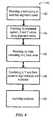
- FIG. 6illustrates a flow chart of an exemplary method 100 for aligning template 18 and substrate 12 .
- a field 70 having multiple sub-fields 92 on the edge 74 a of substrate 12may be provided.
- Alignment system 90may be configured to be in optical communication with alignment marks 72 of field 70 .
- Alignment marks 72may be positioned at outer boundary of field 70 .
- Each sub-field 92may comprise multiple alignment marks 72 a.
- at least one potentially yielding sub-field 92may be identified. Potentially yielding sub-fields 92 may have one or more potentially yielding dies.
- alignment measurement system 90may be re-configured such that alignment measurement units 62 capture alignment marks 72 a within potentially yielding sub-field 92 or a combination of one or more potentially yielding sub-fields 92 .
- alignment measurement system 90may be repositioned to be in optical communication with alignment marks 72 a of the potentially yielding sub-field 92 .
- alignment measurement system 90may be repositioned in optical communication with alignment marks 72 a but outside of a beam path from an energy source focused through template 18 for solidification of polymerizable material 34 .
- potentially yielding field 70 amay be imprinted to provide for one or more yielding dies with suitable alignment.
- alignment data from phase information using alignment marks 72 a of sub-field of substrate 12 and overlaying template alignment marksmay be collected.
- Imagese.g., moiré first order microscope images
- Normal distance between alignment marks 72 a and template alignment marksmay be altered (e.g., from 100 microns to less than 10 nm).
- Relative spatial parameterse.g., alignment, magnification, distortion parameters, and the like
- template 18may align with sub-field 92 of substrate 12 .
- Polymerizable material 34may be deposited on area in superimposition with sub-field 92 of substrate.
- Template 18may be positioned in contact with polymerizable material 34 and polymerizable material 34 may conform between template 18 and substrate 12 .
- Polymerizable material 34may be solidified forming patterned layer 46 .
- Template 18may be separated from polymerizable material 34 forming potentially yielding die in sub-field 92 .
- alignment between template 18 and substrate 12 on edge 74 of substrate 12may include the use of alignment system 60 or 90 and a theta measuring unit 120 .
- Exemplary theta measuring units 120may include laser interferometers, capacitance sensors, and/or any other precision sensors having a pre-determined accuracy.
- at least two alignment marks 72 and/or alignment marks 72 a within each field 70 or sub-field 92may provide X and Y values for alignment.
- alignment marks 72may provide X and Y values for field 70 b.
- Data obtained from the theta measuring unit 120may be combined with the X and Y values to provide sufficient data for alignment of x, y, and theta. It should be noted that by using only x, y and theta, magnification detection may be eliminated in sub-field 92 alignment.
- FIG. 8illustrates an exemplary method 140 for aligning template 18 and substrate 12 using a theta measuring unit 120 .
- a step 142at least one field 70 b having at least two alignment marks 72 may be provided.
- alignment system 60 or 90may provide X and Y values using alignment marks 72 .
- theta measuring unit 120may provide the theta value.
- X, Y, and theta valuesmay be combined to provide for alignment of template 18 and substrate 12 .
- substratemay be imprinted.
- alignment between template 18 and substrate 12 on edge 74 of substrate 12may include the use of alignment marks 72 on adjacent fields 70 .
- alignment on the edge 74 of substrate 12may contain a field 70 d having a potentially yielding sub-field 92 .
- the potentially yielding sub-field 92may only contain one viable alignment mark 72
- alignment marks 72 from adjacent fields 70 e, 70 f, and/or 70 gmay be used to facilitate alignment between template 18 and substrate 12 for imprinting potentially yielding field 70 d.
Landscapes
- Engineering & Computer Science (AREA)
- Physics & Mathematics (AREA)
- General Physics & Mathematics (AREA)
- Nanotechnology (AREA)
- Chemical & Material Sciences (AREA)
- Crystallography & Structural Chemistry (AREA)
- Theoretical Computer Science (AREA)
- Multimedia (AREA)
- Mathematical Physics (AREA)
- Condensed Matter Physics & Semiconductors (AREA)
- Manufacturing & Machinery (AREA)
- Mechanical Engineering (AREA)
- Shaping Of Tube Ends By Bending Or Straightening (AREA)
- Exposure Of Semiconductors, Excluding Electron Or Ion Beam Exposure (AREA)
Abstract
Description
- This application claims the benefit under 35 U.S.C. §119(e)(1) of U.S. Provisional Patent Application No. 61/111,102, filed Nov. 4, 2008, which is hereby incorporated by reference herein in its entirety.
- Nano-fabrication includes the fabrication of very small structures that have features on the order of 100 nanometers or smaller. One application in which nano-fabrication has had a sizeable impact is in the processing of integrated circuits. The semiconductor processing industry continues to strive for larger production yields while increasing the circuits per unit area formed on a substrate, therefore nano-fabrication becomes increasingly important. Nano-fabrication provides greater process control while allowing continued reduction of the minimum feature dimensions of the structures formed. Other areas of development in which nano-fabrication has been employed include biotechnology, optical technology, mechanical systems, and the like.
- An exemplary nano-fabrication technique in use today is commonly referred to as imprint lithography. Exemplary imprint lithography processes are described in detail in numerous publications, such as U.S. Patent Publication No. 2004/0065976, U.S. Patent Publication No. 2004/0065252, and U.S. Pat. No. 6,936,194, all of which are hereby incorporated by reference.
- An imprint lithography technique disclosed in each of the aforementioned U.S. patent publications and patent includes formation of a relief pattern in a formable layer (polymerizable) and transferring a pattern corresponding to the relief pattern into an underlying substrate. The substrate may be coupled to a motion stage to obtain a desired positioning to facilitate the patterning process. The patterning process uses a template spaced apart from the substrate and a formable liquid applied between the template and the substrate. The formable liquid is solidified to form a rigid layer that has a pattern conforming to a shape of the surface of the template that contacts the formable liquid. After solidification, the template is separated from the rigid layer such that the template and the substrate are spaced apart. The substrate and the solidified layer are then subjected to additional processes to transfer a relief image into the substrate that corresponds to the pattern in the solidified layer.
- So that the present invention may be understood in more detail, a description of embodiments of the invention is provided with reference to the embodiments illustrated in the appended drawings. It is to be noted, however, that the appended drawings illustrate only typical embodiments of the invention, and are therefore not to be considered limiting of the scope.
FIG. 1 illustrates a simplified side view of a lithographic system in accordance with an embodiment of the present invention.FIG. 2 illustrates a simplified side view of the substrate shown inFIG. 1 having a patterned layer positioned thereon.FIG. 3 illustrates a simplified top down view of an alignment system having multiple alignment measurement units about a field.FIG. 4 illustrates a simplified top down view of a substrate.FIGS. 5A-5E illustrate exemplary reconfigurable alignment systems.FIG. 6 illustrates a flow chart of an exemplary method for aligning a template and a substrate.FIG. 7 illustrates a simplified top down view of a portion of a substrate.FIG. 8 illustrates a flow chart of an exemplary method for aligning a template and a substrate.FIG. 9 illustrates a simplified top down view of a portion of a substrate.- Referring to the figures, and particularly to
FIG. 1 , illustrated therein is alithographic system 10 used to form a relief pattern onsubstrate 12.Substrate 12 may be coupled tosubstrate chuck 14. As illustrated,substrate chuck 14 is a vacuum chuck.Substrate chuck 14, however, may be any chuck including, but not limited to, vacuum, pin-type, groove-type, electrostatic, electromagnetic, and/or the like. Exemplary chucks are described in U.S. Pat. No. 6,873,087, which is hereby incorporated by reference. Substrate 12 andsubstrate chuck 14 may be further supported by stage16. Stage16 may provide motion along the x-, y-, and z-axes. Stage16,substrate 12, andsubstrate chuck 14 may also be positioned on a base (not shown).- Spaced-apart from
substrate 12 is atemplate 18.Template 18 generally includes amesa 20 extending therefrom towardssubstrate 12,mesa 20 having apatterning surface 22 thereon. Further,mesa 20 may be referred to asmold 20.Patterning surface 22 may be used to pattern a single field ontemplate 18 using a step-and-repeat process as described herein.Template 18 and/ormold 20 may be formed from such materials including, but not limited to, fused-silica, quartz, silicon, organic polymers, siloxane polymers, borosilicate glass, fluorocarbon polymers, metal, hardened sapphire, and/or the like. As illustrated,patterning surface 22 comprises features defined by a plurality of spaced-apart recesses 24 and/orprotrusions 26, though embodiments of the present invention are not limited to such configurations.Patterning surface 22 may define any original pattern that forms the basis of a pattern to be formed onsubstrate 12. Template 18 may be coupled to chuck28. Chuck28 may be configured as, but not limited to, vacuum, pin-type, groove-type, electrostatic, electromagnetic, and/or other similar chuck types. Exemplary chucks are further described in U.S. Pat. No. 6,873,087, which is hereby incorporated by reference. Further,chuck 28 may be coupled to imprinthead 30 such that chuck28 and/orimprint head 30 may be configured to facilitate movement oftemplate 18.System 10 may further comprise afluid dispense system 32.Fluid dispense system 32 may be used to depositpolymerizable material 34 onsubstrate 12.Polymerizable material 34 may be positioned uponsubstrate 12 using techniques such as drop dispense, spin-coating, dip coating, chemical vapor deposition (CVD), physical vapor deposition (PVD), thin film deposition, thick film deposition, and/or the like.Polymerizable material 34 may be disposed uponsubstrate 12 before and/or after a desired volume is defined betweenmold 20 andsubstrate 12 depending on design considerations.Polymerizable material 34 may comprise a monomer mixture as described in U.S. Pat. No. 7,157,036 and U.S. Patent Publication No. 2005/0187339, all of which are hereby incorporated by reference.- Referring to
FIGS. 1 and 2 ,system 10 may further comprise anenergy source 38 coupled todirect energy 40 alongpath 42.Imprint head 30 and stage16 may be configured to positiontemplate 18 andsubstrate 12 in superimposition withpath 42.System 10 may be regulated by aprocessor 54 in communication with stage16,imprint head 30,fluid dispense system 32, and/orsource 38, and may operate on a computer readable program stored inmemory 56. - Either
imprint head 30, stage16, or both vary a distance betweenmold 20 andsubstrate 12 to define a desired volume therebetween that is filled bypolymerizable material 34. For example,imprint head 30 may apply a force totemplate 18 such thatmold 20 contactspolymerizable material 34. After the desired volume is filled withpolymerizable material 34,source 38 producesenergy 40, e.g., ultraviolet radiation, causingpolymerizable material 34 to solidify and/or cross-link conforming to shape of asurface 44 ofsubstrate 12 and patterningsurface 22, defining a patternedlayer 46 onsubstrate 12.Patterned layer 46 may comprise aresidual layer 48 and a plurality of features shown asprotrusions 50 andrecessions 52, withprotrusions 50 having thickness t1and residual layer having a thickness t2.Template 18 may be separated from patternedlayer 46 may used to pattern another field in a step-and-repeat process. - The above-mentioned system and process may be further employed in imprint lithography processes and systems referred to in U.S. Pat. No. 6,932,934, U.S. Patent Publication No. 2004/0124566, U.S. Patent Publication No. 2004/0188381, and U.S. Patent Publication No. 2004/0211754, each of which is hereby incorporated by reference.
- Ascertaining a desired alignment between
template 18 and a field ofsubstrate 12 may aid in the facilitation of pattern transfer betweentemplate 18 andsubstrate 12. To facilitate alignment, an alignment system utilizing alignment marks on thetemplate 18 and/orsubstrate 12 may be used with one alignment mark of the pair being disposed on thetemplate 18, and the remaining alignment mark being positioned on thesubstrate 12.FIG. 3 illustrates a simplified view of analignment system 60 having multiple alignment measurement units62 (e.g., microscopes). Examples of alignment marks andalignment systems 60 for use in imprint lithography processes are described in detail in U.S. Pat. No. 7,136,150, and U.S. Pat. No. 7,070,405, U.S. Pat. No. 6,916,584, and U.S. Patent Publication No. 2007/0231421, all of which are hereby incorporated by reference. Alignment system 60 may be used for a field-by-field alignment process. As illustrated inFIGS. 1 ,3, and4, during imprinting, stage16 may be moved such thattemplate 18 is oriented over the desiredfield 70 of thesubstrate 12 based on coordinates stored inmemory 54. Eachfield 70 of thesubstrate 12 may include two or more alignment marks72 corresponding to alignment marks on thetemplate 18. The alignment marks on thetemplate 18 may then be aligned with alignment marks72 at aspecific field 70 being imprinted on thesubstrate 12. Once thefield 70 is imprinted, stage16 may be moved to orienttemplate 18 over anotherfield 70 of thesubstrate 12. As such, alignment may be conducted withinindividual fields 70 of thesubstrate 12. On theedge 74 ofsubstrate 12, however,portions 76 offields 70 may be outside of the area ofsubstrate 12 leading to alignment error onedge 74 ofsubstrate 12 and, as such, a decrease in die yield.FIGS. 5A and 5B illustrate an exemplaryreconfigurable alignment system 90. Generally, insystem 90, alignment marks72amay be present, not only at the corners offield 70a,but also may be present within each sub-field92 offield 70a.Field 70amay be divided according to the number ofsub-fields 92 withinfield 70a.For example, inFIG. 5A , field70aincludes eightpossible sub-fields 92; however, any number ofsub-fields 92 may be withinfield 70adepending on design considerations. Each sub-field92 may include one or more potentially yielding dies.- Further, each sub-field92 may contain multiple alignment marks72a.Placement of alignment marks72awithin
field 70aand/orsub-field 92 may be designed to limit the surface area allocated to alignment marks72aonsubstrate 12. In one example, alignment marks72amay be within each corner of thesub-field 92. In another example, alignment marks72amay be placed in a gap betweensub-fields 92. In another example, alignment marks72amay be placed in a gap between potentially yielding dies. - At the edge of
substrate 12, not all sub-fields92 provide yielding dies as described above. As illustrated inFIG. 5A , potentially yielding sub-fields92 are marked with hatched box. In this example, row R1provides for no potentially yielding sub-fields92. In the magnification offield 70aon theedge 74a,only four of the eight sub-fields92 may be considered potentially yielding sub-fields. - In one example,
alignment measurement system 90 may be reconfigured to detect alignment marks72ain potentially yielding sub-fields92 in addition to or in lieu of alignment marks72 offield 70. Generally,alignment measurement system 90 is configured to not only detect alignment marks72 within one or more corners offield 90, but also is configured to detect alignment marks72awithinsub-fields 92. As illustrated inFIG. 5B ,alignment measurement units 62 withinregion 94 may be re-configured to detect alignment marks72awithin the potentially yieldingsub-field 92 in addition to or in lieu of alignment marks70 offield 90. For example,alignment measurement units 62 may be moveably positioned (e.g., movement in x, y or z direction to physically relocate to be in optical communication with at least onealignment mark 72asuitable for detection) and/or reconfigured (e.g., configured with additional hardware to provide optical communication with at least onealignment mark 72asuitable for detection). - In another example, as illustrated in
FIGS. 5B-5D , re-configuration of thealignment measurement system 90 may be in apattern 208 that provides for detection of one or more sub-fields92. For example, inFIG. 5C ,field 70amay be divided into four quadrants, Q1, Q2, Q3, and Q4. Each quadrant Q may be formed of at least two sub-fields92. Thealignment measurement system 90 may be re-configured to apattern 208 that provides for detection of a quadrant Q. Thealignment measurement system 90 may then be moved to each quadrant Q1-4to detect alignment marks within each sub-field92. - To facilitate movement without increasing particle generation and/or to increase throughput,
alignment measurement system 90 may driven by ascanning stage 200 as illustrated inFIG. 5D .Alignment measurement system 90 or portions ofalignment measurement system 90 may be fixably connected to scanningstage 200. Scanning stage 200 may comprise a first direction stage202 (e.g., X stage) adjacent to a second direction stage204 (e.g., Y stage).X stage 202 may include a plurality ofsides 206.Sides 206 may be positioned about anopen area 208.Sides 206 may form any shape formation including, but limited to, square, rectangle, hexagonal, circular, and/or any fanciful shape.Y stage 204 may includes a plurality ofside 210.Sides 210 may be positioned aboutopen area 208.Sides 210 may form any shape formation including, but limited to, square, rectangle, hexagonal, circular, and/or any fanciful shape. Shape formation ofsides 210 may be similar to shape ofsides 206 or different from shape ofsides 206.- In another example, as illustrated in
FIG. 5E , one or more additionalalignment measurement units 62xmay be added toalignment measurement system 60 shown inFIG. 3 . Typical numbers and placement ofalignment measurement units 62 are further described in U.S. Pat. No. 7,292,326 and U.S. Ser. No. 11/000,321, which are both hereby incorporated by reference in their entirety. Additionalalignment measurement units 62xmay be introduced into the systems described in these references and configured to detect alignment marks72apositioned within sub-fields92. For example, as illustrated inFIG. 5E ,alignment measurement units region 95 may be configured to detect alignment marks72ain the potentially yieldingsub-field 92. FIG. 6 illustrates a flow chart of anexemplary method 100 for aligningtemplate 18 andsubstrate 12. In astep 102, afield 70 havingmultiple sub-fields 92 on theedge 74aofsubstrate 12 may be provided.Alignment system 90 may be configured to be in optical communication with alignment marks72 offield 70. Alignment marks72 may be positioned at outer boundary offield 70. Each sub-field92 may comprise multiple alignment marks72a.In astep 104, at least one potentially yieldingsub-field 92 may be identified. Potentially yielding sub-fields92 may have one or more potentially yielding dies. In astep 106,alignment measurement system 90 may be re-configured such thatalignment measurement units 62 capture alignment marks72awithin potentially yieldingsub-field 92 or a combination of one or more potentially yielding sub-fields92. For example,alignment measurement system 90 may be repositioned to be in optical communication with alignment marks72aof the potentially yieldingsub-field 92. In one embodiment,alignment measurement system 90 may be repositioned in optical communication with alignment marks72abut outside of a beam path from an energy source focused throughtemplate 18 for solidification ofpolymerizable material 34. In astep 108, potentially yieldingfield 70amay be imprinted to provide for one or more yielding dies with suitable alignment. For example, alignment data from phase information using alignment marks72aof sub-field ofsubstrate 12 and overlaying template alignment marks may be collected. Images (e.g., moiré first order microscope images) may be captured by diffracting light from one of alignment marks72aor template alignment marks. Normal distance between alignment marks72aand template alignment marks may be altered (e.g., from 100 microns to less than 10 nm). Relative spatial parameters (e.g., alignment, magnification, distortion parameters, and the like) betweensubstrate 12 andtemplate 18 may be determined using the images. Using the relative spatial parameters,template 18 may align withsub-field 92 ofsubstrate 12.Polymerizable material 34 may be deposited on area in superimposition withsub-field 92 of substrate.Template 18 may be positioned in contact withpolymerizable material 34 andpolymerizable material 34 may conform betweentemplate 18 andsubstrate 12.Polymerizable material 34 may be solidified forming patternedlayer 46.Template 18 may be separated frompolymerizable material 34 forming potentially yielding die insub-field 92.- Referring to
FIGS. 1 ,3 and7, alignment betweentemplate 18 andsubstrate 12 onedge 74 ofsubstrate 12 may include the use ofalignment system theta measuring unit 120. Exemplarytheta measuring units 120 may include laser interferometers, capacitance sensors, and/or any other precision sensors having a pre-determined accuracy. Generally, at least two alignment marks72 and/or alignment marks72awithin eachfield 70 orsub-field 92 may provide X and Y values for alignment. For example, as shown in the figures, alignment marks72 may provide X and Y values forfield 70b.Data obtained from thetheta measuring unit 120 may be combined with the X and Y values to provide sufficient data for alignment of x, y, and theta. It should be noted that by using only x, y and theta, magnification detection may be eliminated insub-field 92 alignment. FIG. 8 illustrates anexemplary method 140 for aligningtemplate 18 andsubstrate 12 using atheta measuring unit 120. In astep 142, at least onefield 70bhaving at least two alignment marks72 may be provided. In astep 144,alignment system step 146,theta measuring unit 120 may provide the theta value. In a step148, X, Y, and theta values may be combined to provide for alignment oftemplate 18 andsubstrate 12. In astep 150, substrate may be imprinted.- Referring to
FIGS. 1 ,3 and9, alignment betweentemplate 18 andsubstrate 12 onedge 74 ofsubstrate 12 may include the use of alignment marks72 onadjacent fields 70. For example, as illustrated inFIG. 9 , alignment on theedge 74 ofsubstrate 12 may contain afield 70dhaving a potentially yieldingsub-field 92. As the potentially yieldingsub-field 92 may only contain oneviable alignment mark 72, alignment marks72 fromadjacent fields template 18 andsubstrate 12 for imprinting potentially yieldingfield 70d.
Claims (20)
Priority Applications (4)
| Application Number | Priority Date | Filing Date | Title |
|---|---|---|---|
| US12/606,274US8432548B2 (en) | 2008-11-04 | 2009-10-27 | Alignment for edge field nano-imprinting |
| PCT/US2009/005869WO2010053519A2 (en) | 2008-11-04 | 2009-10-29 | Alignment for edge field nano-imprinting |
| KR1020117012921AKR101681506B1 (en) | 2008-11-04 | 2009-10-29 | Alignment for edge field nano-imprinting |
| JP2011535552AJP2012507882A (en) | 2008-11-04 | 2009-10-29 | Alignment for edge field nanoimprint |
Applications Claiming Priority (2)
| Application Number | Priority Date | Filing Date | Title |
|---|---|---|---|
| US11110208P | 2008-11-04 | 2008-11-04 | |
| US12/606,274US8432548B2 (en) | 2008-11-04 | 2009-10-27 | Alignment for edge field nano-imprinting |
Publications (2)
| Publication Number | Publication Date |
|---|---|
| US20100110434A1true US20100110434A1 (en) | 2010-05-06 |
| US8432548B2 US8432548B2 (en) | 2013-04-30 |
Family
ID=42130986
Family Applications (1)
| Application Number | Title | Priority Date | Filing Date |
|---|---|---|---|
| US12/606,274Active2031-07-28US8432548B2 (en) | 2008-11-04 | 2009-10-27 | Alignment for edge field nano-imprinting |
Country Status (5)
| Country | Link |
|---|---|
| US (1) | US8432548B2 (en) |
| JP (1) | JP2012507882A (en) |
| KR (1) | KR101681506B1 (en) |
| TW (1) | TWI413176B (en) |
| WO (1) | WO2010053519A2 (en) |
Cited By (10)
| Publication number | Priority date | Publication date | Assignee | Title |
|---|---|---|---|---|
| US20110084417A1 (en)* | 2009-10-08 | 2011-04-14 | Molecular Imprints, Inc. | Large area linear array nanoimprinting |
| JP2013138175A (en)* | 2011-11-30 | 2013-07-11 | Canon Inc | Imprint device, imprint method, and article manufacturing method |
| CN103226284A (en)* | 2012-01-31 | 2013-07-31 | 佳能株式会社 | Imprint apparatus and method of manufacturing article |
| JP2013197107A (en)* | 2012-03-15 | 2013-09-30 | Canon Inc | Imprint device and article production method |
| WO2017062741A1 (en)* | 2015-10-08 | 2017-04-13 | The Regents Of The University Of Colorado, A Body Corporate | Remote focusing all-optical digital scanning light sheet microscopy for optically cleared tissue sections |
| US10248018B2 (en)* | 2015-03-30 | 2019-04-02 | Canon Kabushiki Kaisha | Imprint apparatus and method of manufacturing article |
| US10611063B2 (en)* | 2013-12-09 | 2020-04-07 | Canon Kabushiki Kaisha | Imprint apparatus, and method of manufacturing article |
| US20210033967A1 (en)* | 2016-06-01 | 2021-02-04 | Canon Kabushiki Kaisha | Method for disposing substrate and method for manufacturing article |
| CN112373173A (en)* | 2020-11-12 | 2021-02-19 | 镇江恒华彩印包装有限责任公司 | Printing plate structure convenient to replace for paper printing and quick replacement method thereof |
| CN114114829A (en)* | 2020-08-26 | 2022-03-01 | 佳能株式会社 | Imprint apparatus and method of manufacturing article |
Families Citing this family (13)
| Publication number | Priority date | Publication date | Assignee | Title |
|---|---|---|---|---|
| NL2005975A (en) | 2010-03-03 | 2011-09-06 | Asml Netherlands Bv | Imprint lithography. |
| JP6188382B2 (en) | 2013-04-03 | 2017-08-30 | キヤノン株式会社 | Imprint apparatus and article manufacturing method |
| JP6604793B2 (en)* | 2015-09-17 | 2019-11-13 | キヤノン株式会社 | Imprint apparatus and article manufacturing method |
| JP6592343B2 (en)* | 2015-11-30 | 2019-10-16 | キヤノン株式会社 | Imprint apparatus and article manufacturing method |
| DK3455676T3 (en) | 2016-07-14 | 2019-12-09 | Morphotonics Holding Bv | DEVICE FOR PRINTING DISCRETE SUBSTRATES WITH A DISCREET FLEXIBLE STAMP |
| US10549313B2 (en)* | 2016-10-31 | 2020-02-04 | Canon Kabushiki Kaisha | Edge field imprint lithography |
| KR102288981B1 (en)* | 2017-04-17 | 2021-08-13 | 에스케이하이닉스 주식회사 | Imprint template and methods of forming imprint patterns |
| KR102775942B1 (en) | 2018-01-26 | 2025-03-07 | 모포토닉스 홀딩 비.브이. | Process and equipment for texturing individual substrates |
| DK3662325T3 (en) | 2018-10-12 | 2021-02-01 | Morphotonics B V | FLEXIBLE STAMP WITH ADJUSTABLE HIGH DIMENSIONAL STABILITY |
| JP7433861B2 (en)* | 2019-11-27 | 2024-02-20 | キヤノン株式会社 | Imprint equipment, imprint method, article manufacturing method, substrate, and mold |
| IL300038A (en) | 2020-07-31 | 2023-03-01 | Morphotonics Holding Bv | Apparatus and process for duplicating texture |
| EP4433871A1 (en) | 2021-11-15 | 2024-09-25 | Morphotonics Holding B.V. | Multi-textured stamp |
| CN115031626B (en)* | 2022-05-05 | 2023-08-18 | 智慧星空(上海)工程技术有限公司 | Substrate coordinate measuring method |
Citations (39)
| Publication number | Priority date | Publication date | Assignee | Title |
|---|---|---|---|---|
| US4869998A (en)* | 1986-05-01 | 1989-09-26 | Smiths Industries Public Limited Company | Intergrated circuit substrates |
| US6018395A (en)* | 1989-09-26 | 2000-01-25 | Canon Kabushiki Kaisha | Alignment system |
| US6071656A (en)* | 1999-07-07 | 2000-06-06 | United Microelectronics Corp. | Photolithography technique utilizing alignment marks at scribe line intersections |
| US6277532B1 (en)* | 1998-10-14 | 2001-08-21 | Nikon Corporation | Charged-particle-beam microlithographic methods for correction of reticle distortions |
| US6368761B1 (en)* | 2000-05-09 | 2002-04-09 | Macronix International Co., Ltd. | Procedure of alignment for optimal wafer exposure pattern |
| US6466301B1 (en)* | 1999-01-25 | 2002-10-15 | Canon Kabushiki Kaisha | Transfer apparatus and transfer method |
| US20030003677A1 (en)* | 2001-06-27 | 2003-01-02 | Canon Kabushiki Kaisha | Alignment method, exposure apparatus and device fabrication method |
| US20040022888A1 (en)* | 2002-08-01 | 2004-02-05 | Sreenivasan Sidlgata V. | Alignment systems for imprint lithography |
| US6724096B2 (en)* | 2001-06-12 | 2004-04-20 | Advanced Micro Devices, Inc. | Die corner alignment structure |
| US20040096759A1 (en)* | 2002-11-15 | 2004-05-20 | Barber Duane B. | Feed forward leveling |
| US20040149687A1 (en)* | 1999-10-29 | 2004-08-05 | University Of Texas System, Board Of Regents, Ut System | Method of manufacturing a vacuum chuck used in imprint lithography |
| US20040163563A1 (en)* | 2000-07-16 | 2004-08-26 | The Board Of Regents, The University Of Texas System | Imprint lithography template having a mold to compensate for material changes of an underlying liquid |
| US20040180276A1 (en)* | 2003-03-14 | 2004-09-16 | Taiwan Semiconductor Manufacturing Co., Ltd. | Determining the maximum number of dies fitting on a semiconductor wafer |
| US6826738B2 (en)* | 2002-05-10 | 2004-11-30 | Pdf Solutions, Inc. | Optimization of die placement on wafers |
| US20050064344A1 (en)* | 2003-09-18 | 2005-03-24 | University Of Texas System Board Of Regents | Imprint lithography templates having alignment marks |
| US6908830B2 (en)* | 2003-06-23 | 2005-06-21 | International Business Machines Corporation | Method for printing marks on the edges of wafers |
| US6916584B2 (en)* | 2002-08-01 | 2005-07-12 | Molecular Imprints, Inc. | Alignment methods for imprint lithography |
| US6954275B2 (en)* | 2000-08-01 | 2005-10-11 | Boards Of Regents, The University Of Texas System | Methods for high-precision gap and orientation sensing between a transparent template and substrate for imprint lithography |
| US20050270516A1 (en)* | 2004-06-03 | 2005-12-08 | Molecular Imprints, Inc. | System for magnification and distortion correction during nano-scale manufacturing |
| US20050271955A1 (en)* | 2004-06-03 | 2005-12-08 | Board Of Regents, The University Of Texas System | System and method for improvement of alignment and overlay for microlithography |
| US7027156B2 (en)* | 2002-08-01 | 2006-04-11 | Molecular Imprints, Inc. | Scatterometry alignment for imprint lithography |
| US20060108541A1 (en)* | 2002-09-02 | 2006-05-25 | Sony Corrporation | Alignment method, alignment substrate, production method for alignment substrate, exposure method, exposure system and mask producing method |
| US20060114450A1 (en)* | 2004-11-30 | 2006-06-01 | Molecular Imprints, Inc. | Interferometric analysis method for the manufacture of nano-scale devices |
| US20060115999A1 (en)* | 2004-12-01 | 2006-06-01 | Molecular Imprints, Inc. | Methods of exposure for the purpose of thermal management for imprint lithography processes |
| US20060126058A1 (en)* | 2004-11-30 | 2006-06-15 | Molecular Imprints, Inc. | Interferometric analysis for the manufacture of nano-scale devices |
| US7245358B2 (en)* | 2004-05-28 | 2007-07-17 | Board Of Regents, The University Of Texas System | Substrate support system |
| US20070228609A1 (en)* | 2006-04-03 | 2007-10-04 | Molecular Imprints, Inc. | Imprinting of Partial Fields at the Edge of the Wafer |
| US20070228610A1 (en)* | 2006-04-03 | 2007-10-04 | Molecular Imprints, Inc. | Method of Concurrently Patterning a Substrate Having a Plurality of Fields and a Plurality of Alignment Marks |
| US20070231421A1 (en)* | 2006-04-03 | 2007-10-04 | Molecular Imprints, Inc. | Enhanced Multi Channel Alignment |
| US20070243655A1 (en)* | 2006-04-18 | 2007-10-18 | Molecular Imprints, Inc. | Self-Aligned Process for Fabricating Imprint Templates Containing Variously Etched Features |
| US7323130B2 (en)* | 2002-12-13 | 2008-01-29 | Molecular Imprints, Inc. | Magnification correction employing out-of-plane distortion of a substrate |
| US7353077B2 (en)* | 2005-07-29 | 2008-04-01 | Taiwan Semiconductor Manufacturing Company | Methods for optimizing die placement |
| US7388663B2 (en)* | 2004-10-28 | 2008-06-17 | Asml Netherlands B.V. | Optical position assessment apparatus and method |
| US20080204696A1 (en)* | 2007-02-28 | 2008-08-28 | Tdk Corporation | Method of alignment |
| US20090026657A1 (en)* | 2007-07-20 | 2009-01-29 | Molecular Imprints, Inc. | Alignment System and Method for a Substrate in a Nano-Imprint Process |
| US20090147237A1 (en)* | 2007-12-05 | 2009-06-11 | Molecular Imprints, Inc. | Spatial Phase Feature Location |
| US20090250840A1 (en)* | 2006-04-18 | 2009-10-08 | Molecular Imprints, Inc. | Template Having Alignment Marks Formed of Contrast Material |
| US7670529B2 (en)* | 2005-12-08 | 2010-03-02 | Molecular Imprints, Inc. | Method and system for double-sided patterning of substrates |
| US20100099259A1 (en)* | 2007-06-20 | 2010-04-22 | Asahi Glass Company, Limited | Polishing composition and method for manufacturing semiconductor integrated circuit device |
Family Cites Families (2)
| Publication number | Priority date | Publication date | Assignee | Title |
|---|---|---|---|---|
| EP0938597B1 (en) | 1996-09-06 | 2003-08-20 | Obducat Aktiebolag | Method for anisotropic etching of structures in conducting materials |
| JP2005167030A (en) | 2003-12-03 | 2005-06-23 | Sony Corp | Mask and exposure method |
- 2009
- 2009-10-27USUS12/606,274patent/US8432548B2/enactiveActive
- 2009-10-29KRKR1020117012921Apatent/KR101681506B1/enactiveActive
- 2009-10-29WOPCT/US2009/005869patent/WO2010053519A2/enactiveApplication Filing
- 2009-10-29JPJP2011535552Apatent/JP2012507882A/ennot_activeWithdrawn
- 2009-10-30TWTW098136910Apatent/TWI413176B/enactive
Patent Citations (54)
| Publication number | Priority date | Publication date | Assignee | Title |
|---|---|---|---|---|
| US4869998A (en)* | 1986-05-01 | 1989-09-26 | Smiths Industries Public Limited Company | Intergrated circuit substrates |
| US6018395A (en)* | 1989-09-26 | 2000-01-25 | Canon Kabushiki Kaisha | Alignment system |
| US6277532B1 (en)* | 1998-10-14 | 2001-08-21 | Nikon Corporation | Charged-particle-beam microlithographic methods for correction of reticle distortions |
| US6466301B1 (en)* | 1999-01-25 | 2002-10-15 | Canon Kabushiki Kaisha | Transfer apparatus and transfer method |
| US6071656A (en)* | 1999-07-07 | 2000-06-06 | United Microelectronics Corp. | Photolithography technique utilizing alignment marks at scribe line intersections |
| US20040149687A1 (en)* | 1999-10-29 | 2004-08-05 | University Of Texas System, Board Of Regents, Ut System | Method of manufacturing a vacuum chuck used in imprint lithography |
| US6873087B1 (en)* | 1999-10-29 | 2005-03-29 | Board Of Regents, The University Of Texas System | High precision orientation alignment and gap control stages for imprint lithography processes |
| US6922906B2 (en)* | 1999-10-29 | 2005-08-02 | Board Of Regents, The University Of Texas System | Apparatus to orientate a body with respect to a surface |
| US6368761B1 (en)* | 2000-05-09 | 2002-04-09 | Macronix International Co., Ltd. | Procedure of alignment for optimal wafer exposure pattern |
| US20040163563A1 (en)* | 2000-07-16 | 2004-08-26 | The Board Of Regents, The University Of Texas System | Imprint lithography template having a mold to compensate for material changes of an underlying liquid |
| US7186483B2 (en)* | 2000-07-16 | 2007-03-06 | Board Of Regents, The University Of Texas System | Method of determining alignment of a template and a substrate having a liquid disposed therebetween |
| US6842229B2 (en)* | 2000-07-16 | 2005-01-11 | Board Of Regents, The University Of Texas System | Imprint lithography template comprising alignment marks |
| US7303383B1 (en)* | 2000-07-16 | 2007-12-04 | Board Of Regents, The University Of Texas System | Imprint lithography system to produce light to impinge upon and polymerize a liquid in superimposition with template overlay marks |
| US6902853B2 (en)* | 2000-07-16 | 2005-06-07 | Board Of Regents, The University Of Texas System | Dual wavelength method of determining a relative position of a substrate and a template |
| US6921615B2 (en)* | 2000-07-16 | 2005-07-26 | Board Of Regents, The University Of Texas System | High-resolution overlay alignment methods for imprint lithography |
| US6954275B2 (en)* | 2000-08-01 | 2005-10-11 | Boards Of Regents, The University Of Texas System | Methods for high-precision gap and orientation sensing between a transparent template and substrate for imprint lithography |
| US6724096B2 (en)* | 2001-06-12 | 2004-04-20 | Advanced Micro Devices, Inc. | Die corner alignment structure |
| US20030003677A1 (en)* | 2001-06-27 | 2003-01-02 | Canon Kabushiki Kaisha | Alignment method, exposure apparatus and device fabrication method |
| US6826738B2 (en)* | 2002-05-10 | 2004-11-30 | Pdf Solutions, Inc. | Optimization of die placement on wafers |
| US7281921B2 (en)* | 2002-08-01 | 2007-10-16 | Molecular Imprints, Inc. | Scatterometry alignment for imprint lithography |
| US6916584B2 (en)* | 2002-08-01 | 2005-07-12 | Molecular Imprints, Inc. | Alignment methods for imprint lithography |
| US20040022888A1 (en)* | 2002-08-01 | 2004-02-05 | Sreenivasan Sidlgata V. | Alignment systems for imprint lithography |
| US7070405B2 (en)* | 2002-08-01 | 2006-07-04 | Molecular Imprints, Inc. | Alignment systems for imprint lithography |
| US7027156B2 (en)* | 2002-08-01 | 2006-04-11 | Molecular Imprints, Inc. | Scatterometry alignment for imprint lithography |
| US20060108541A1 (en)* | 2002-09-02 | 2006-05-25 | Sony Corrporation | Alignment method, alignment substrate, production method for alignment substrate, exposure method, exposure system and mask producing method |
| US20040096759A1 (en)* | 2002-11-15 | 2004-05-20 | Barber Duane B. | Feed forward leveling |
| US7323130B2 (en)* | 2002-12-13 | 2008-01-29 | Molecular Imprints, Inc. | Magnification correction employing out-of-plane distortion of a substrate |
| US7033847B2 (en)* | 2003-03-14 | 2006-04-25 | Taiwan Semiconductor Manufacturing Co., Ltd. | Determining the maximum number of dies fitting on a semiconductor wafer |
| US20040180276A1 (en)* | 2003-03-14 | 2004-09-16 | Taiwan Semiconductor Manufacturing Co., Ltd. | Determining the maximum number of dies fitting on a semiconductor wafer |
| US6908830B2 (en)* | 2003-06-23 | 2005-06-21 | International Business Machines Corporation | Method for printing marks on the edges of wafers |
| US20050064344A1 (en)* | 2003-09-18 | 2005-03-24 | University Of Texas System Board Of Regents | Imprint lithography templates having alignment marks |
| US20080153312A1 (en)* | 2004-02-18 | 2008-06-26 | Molecular Imprints, Inc. | Methods for Exposure for the Purpose of Thermal Management for Imprint Lithography Processes |
| US7245358B2 (en)* | 2004-05-28 | 2007-07-17 | Board Of Regents, The University Of Texas System | Substrate support system |
| US20080204693A1 (en)* | 2004-05-28 | 2008-08-28 | Board Of Regents, The University Of Texas System | Substrate Support Method |
| US20050270516A1 (en)* | 2004-06-03 | 2005-12-08 | Molecular Imprints, Inc. | System for magnification and distortion correction during nano-scale manufacturing |
| US7170589B2 (en)* | 2004-06-03 | 2007-01-30 | Molecular Imprints, Inc. | Apparatus to vary dimensions of a substrate during nano-scale manufacturing |
| US20050271955A1 (en)* | 2004-06-03 | 2005-12-08 | Board Of Regents, The University Of Texas System | System and method for improvement of alignment and overlay for microlithography |
| US20050269745A1 (en)* | 2004-06-03 | 2005-12-08 | Molecular Imprints, Inc. | Method of varying dimensions of a substrate during nano-scale manufacturing |
| US7388663B2 (en)* | 2004-10-28 | 2008-06-17 | Asml Netherlands B.V. | Optical position assessment apparatus and method |
| US20060126058A1 (en)* | 2004-11-30 | 2006-06-15 | Molecular Imprints, Inc. | Interferometric analysis for the manufacture of nano-scale devices |
| US7292326B2 (en)* | 2004-11-30 | 2007-11-06 | Molecular Imprints, Inc. | Interferometric analysis for the manufacture of nano-scale devices |
| US20060114450A1 (en)* | 2004-11-30 | 2006-06-01 | Molecular Imprints, Inc. | Interferometric analysis method for the manufacture of nano-scale devices |
| US20060115999A1 (en)* | 2004-12-01 | 2006-06-01 | Molecular Imprints, Inc. | Methods of exposure for the purpose of thermal management for imprint lithography processes |
| US7353077B2 (en)* | 2005-07-29 | 2008-04-01 | Taiwan Semiconductor Manufacturing Company | Methods for optimizing die placement |
| US7670529B2 (en)* | 2005-12-08 | 2010-03-02 | Molecular Imprints, Inc. | Method and system for double-sided patterning of substrates |
| US20070228610A1 (en)* | 2006-04-03 | 2007-10-04 | Molecular Imprints, Inc. | Method of Concurrently Patterning a Substrate Having a Plurality of Fields and a Plurality of Alignment Marks |
| US20070228609A1 (en)* | 2006-04-03 | 2007-10-04 | Molecular Imprints, Inc. | Imprinting of Partial Fields at the Edge of the Wafer |
| US20070231421A1 (en)* | 2006-04-03 | 2007-10-04 | Molecular Imprints, Inc. | Enhanced Multi Channel Alignment |
| US20070243655A1 (en)* | 2006-04-18 | 2007-10-18 | Molecular Imprints, Inc. | Self-Aligned Process for Fabricating Imprint Templates Containing Variously Etched Features |
| US20090250840A1 (en)* | 2006-04-18 | 2009-10-08 | Molecular Imprints, Inc. | Template Having Alignment Marks Formed of Contrast Material |
| US20080204696A1 (en)* | 2007-02-28 | 2008-08-28 | Tdk Corporation | Method of alignment |
| US20100099259A1 (en)* | 2007-06-20 | 2010-04-22 | Asahi Glass Company, Limited | Polishing composition and method for manufacturing semiconductor integrated circuit device |
| US20090026657A1 (en)* | 2007-07-20 | 2009-01-29 | Molecular Imprints, Inc. | Alignment System and Method for a Substrate in a Nano-Imprint Process |
| US20090147237A1 (en)* | 2007-12-05 | 2009-06-11 | Molecular Imprints, Inc. | Spatial Phase Feature Location |
Cited By (16)
| Publication number | Priority date | Publication date | Assignee | Title |
|---|---|---|---|---|
| US20110084417A1 (en)* | 2009-10-08 | 2011-04-14 | Molecular Imprints, Inc. | Large area linear array nanoimprinting |
| JP2013138175A (en)* | 2011-11-30 | 2013-07-11 | Canon Inc | Imprint device, imprint method, and article manufacturing method |
| CN104765249A (en)* | 2011-11-30 | 2015-07-08 | 佳能株式会社 | Imprint apparatus, imprint method, and article manufacturing method |
| US9915868B2 (en) | 2011-11-30 | 2018-03-13 | Canon Kabushiki Kaisha | Imprint apparatus, imprint method, and article manufacturing method |
| CN103226284A (en)* | 2012-01-31 | 2013-07-31 | 佳能株式会社 | Imprint apparatus and method of manufacturing article |
| US9616613B2 (en) | 2012-01-31 | 2017-04-11 | Canon Kabushiki Kaisha | Imprint apparatus including alignment and overlay measurement |
| JP2013197107A (en)* | 2012-03-15 | 2013-09-30 | Canon Inc | Imprint device and article production method |
| US10611063B2 (en)* | 2013-12-09 | 2020-04-07 | Canon Kabushiki Kaisha | Imprint apparatus, and method of manufacturing article |
| US10248018B2 (en)* | 2015-03-30 | 2019-04-02 | Canon Kabushiki Kaisha | Imprint apparatus and method of manufacturing article |
| WO2017062741A1 (en)* | 2015-10-08 | 2017-04-13 | The Regents Of The University Of Colorado, A Body Corporate | Remote focusing all-optical digital scanning light sheet microscopy for optically cleared tissue sections |
| US20210033967A1 (en)* | 2016-06-01 | 2021-02-04 | Canon Kabushiki Kaisha | Method for disposing substrate and method for manufacturing article |
| US11774850B2 (en)* | 2016-06-01 | 2023-10-03 | Canon Kabushiki Kaisha | Method for disposing substrate and method for manufacturing article |
| CN114114829A (en)* | 2020-08-26 | 2022-03-01 | 佳能株式会社 | Imprint apparatus and method of manufacturing article |
| US20220063177A1 (en)* | 2020-08-26 | 2022-03-03 | Canon Kabushiki Kaisha | Imprint apparatus and method of manufacturing article |
| US12162206B2 (en)* | 2020-08-26 | 2024-12-10 | Canon Kabushiki Kaisha | Imprint apparatus and method of manufacturing article |
| CN112373173A (en)* | 2020-11-12 | 2021-02-19 | 镇江恒华彩印包装有限责任公司 | Printing plate structure convenient to replace for paper printing and quick replacement method thereof |
Also Published As
| Publication number | Publication date |
|---|---|
| KR101681506B1 (en) | 2016-12-01 |
| WO2010053519A3 (en) | 2010-09-02 |
| JP2012507882A (en) | 2012-03-29 |
| TW201019388A (en) | 2010-05-16 |
| US8432548B2 (en) | 2013-04-30 |
| KR20110083713A (en) | 2011-07-20 |
| WO2010053519A2 (en) | 2010-05-14 |
| TWI413176B (en) | 2013-10-21 |
Similar Documents
| Publication | Publication Date | Title |
|---|---|---|
| US8432548B2 (en) | Alignment for edge field nano-imprinting | |
| CN100460805C (en) | Application of scatterometry alignment in imprint lithography | |
| US7785096B2 (en) | Enhanced multi channel alignment | |
| EP2171537B1 (en) | Alignment system and method for a substrate in a nano-imprint process | |
| US7670529B2 (en) | Method and system for double-sided patterning of substrates | |
| US8865046B2 (en) | Imprinting of partial fields at the edge of the wafer | |
| US7780893B2 (en) | Method of concurrently patterning a substrate having a plurality of fields and a plurality of alignment marks | |
| US8850980B2 (en) | Tessellated patterns in imprint lithography | |
| CN100504598C (en) | High resolution overlay alignment method and system for use in lithographic processes | |
| US20110084417A1 (en) | Large area linear array nanoimprinting | |
| US20110219635A1 (en) | Method of aligning a first article relative to a second article and an apparatus for aligning a first article relative to a second article | |
| US20080153312A1 (en) | Methods for Exposure for the Purpose of Thermal Management for Imprint Lithography Processes | |
| US8628712B2 (en) | Misalignment management | |
| US20090147237A1 (en) | Spatial Phase Feature Location | |
| US20090148032A1 (en) | Alignment Using Moire Patterns | |
| US8231821B2 (en) | Substrate alignment | |
| US12405537B2 (en) | Devices, systems, and methods for the transformation and cropping of drop patterns | |
| US20240178042A1 (en) | Systems, devices, and methods for registering a superstrate of an imprint tool |
Legal Events
| Date | Code | Title | Description |
|---|---|---|---|
| AS | Assignment | Owner name:MOLECULAR IMPRINTS, INC.,TEXAS Free format text:ASSIGNMENT OF ASSIGNORS INTEREST;ASSIGNORS:CHOI, BYUNG-JIN;NIMMAKAYALA, PAWAN KUMAR;SCHUMAKER, PHILIP D.;REEL/FRAME:023551/0765 Effective date:20091120 Owner name:MOLECULAR IMPRINTS, INC., TEXAS Free format text:ASSIGNMENT OF ASSIGNORS INTEREST;ASSIGNORS:CHOI, BYUNG-JIN;NIMMAKAYALA, PAWAN KUMAR;SCHUMAKER, PHILIP D.;REEL/FRAME:023551/0765 Effective date:20091120 | |
| FEPP | Fee payment procedure | Free format text:PAYOR NUMBER ASSIGNED (ORIGINAL EVENT CODE: ASPN); ENTITY STATUS OF PATENT OWNER: LARGE ENTITY | |
| STCF | Information on status: patent grant | Free format text:PATENTED CASE | |
| AS | Assignment | Owner name:MII NEWCO, INC., TEXAS Free format text:ASSIGNMENT OF JOINT OWNERSHIP;ASSIGNOR:MOLECULAR IMPRINTS, INC.;REEL/FRAME:033329/0280 Effective date:20140710 | |
| AS | Assignment | Owner name:CANON NANOTECHNOLOGIES, INC., TEXAS Free format text:CHANGE OF NAME;ASSIGNOR:MOLECULAR IMPRINTS, INC.;REEL/FRAME:033400/0184 Effective date:20140417 | |
| AS | Assignment | Owner name:MOLECULAR IMPRINTS, INC., TEXAS Free format text:CHANGE OF NAME;ASSIGNOR:MII NEWCO, INC.;REEL/FRAME:033449/0684 Effective date:20140423 | |
| AS | Assignment | Owner name:MOLECULAR IMPRINTS, INC., TEXAS Free format text:CONFIRMATORY ASSIGNMENT OF JOINT PATENT OWNERSHIP;ASSIGNOR:CANON NANOTECHNOLOGIES, INC.;REEL/FRAME:035507/0559 Effective date:20150427 | |
| FPAY | Fee payment | Year of fee payment:4 | |
| AS | Assignment | Owner name:JP MORGAN CHASE BANK, N.A., NEW YORK Free format text:PATENT SECURITY AGREEMENT;ASSIGNORS:MAGIC LEAP, INC.;MOLECULAR IMPRINTS, INC.;MENTOR ACQUISITION ONE, LLC;REEL/FRAME:050138/0287 Effective date:20190820 | |
| AS | Assignment | Owner name:CITIBANK, N.A., NEW YORK Free format text:ASSIGNMENT OF SECURITY INTEREST IN PATENTS;ASSIGNOR:JPMORGAN CHASE BANK, N.A.;REEL/FRAME:050967/0138 Effective date:20191106 | |
| MAFP | Maintenance fee payment | Free format text:PAYMENT OF MAINTENANCE FEE, 8TH YEAR, LARGE ENTITY (ORIGINAL EVENT CODE: M1552); ENTITY STATUS OF PATENT OWNER: LARGE ENTITY Year of fee payment:8 | |
| MAFP | Maintenance fee payment | Free format text:PAYMENT OF MAINTENANCE FEE, 12TH YEAR, LARGE ENTITY (ORIGINAL EVENT CODE: M1553); ENTITY STATUS OF PATENT OWNER: LARGE ENTITY Year of fee payment:12 |