US20100110430A1 - Device for sorting and concentrating electromagnetic energy and apparatus comprising at least one such device - Google Patents
Device for sorting and concentrating electromagnetic energy and apparatus comprising at least one such deviceDownload PDFInfo
- Publication number
- US20100110430A1 US20100110430A1US12/532,499US53249908AUS2010110430A1US 20100110430 A1US20100110430 A1US 20100110430A1US 53249908 AUS53249908 AUS 53249908AUS 2010110430 A1US2010110430 A1US 2010110430A1
- Authority
- US
- United States
- Prior art keywords
- structures
- concentrator
- different
- light
- impinged
- Prior art date
- Legal status (The legal status is an assumption and is not a legal conclusion. Google has not performed a legal analysis and makes no representation as to the accuracy of the status listed.)
- Granted
Links
Images


Classifications
- G—PHYSICS
- G02—OPTICS
- G02B—OPTICAL ELEMENTS, SYSTEMS OR APPARATUS
- G02B5/00—Optical elements other than lenses
- G02B5/008—Surface plasmon devices
- B—PERFORMING OPERATIONS; TRANSPORTING
- B82—NANOTECHNOLOGY
- B82Y—SPECIFIC USES OR APPLICATIONS OF NANOSTRUCTURES; MEASUREMENT OR ANALYSIS OF NANOSTRUCTURES; MANUFACTURE OR TREATMENT OF NANOSTRUCTURES
- B82Y20/00—Nanooptics, e.g. quantum optics or photonic crystals
- G—PHYSICS
- G01—MEASURING; TESTING
- G01J—MEASUREMENT OF INTENSITY, VELOCITY, SPECTRAL CONTENT, POLARISATION, PHASE OR PULSE CHARACTERISTICS OF INFRARED, VISIBLE OR ULTRAVIOLET LIGHT; COLORIMETRY; RADIATION PYROMETRY
- G01J3/00—Spectrometry; Spectrophotometry; Monochromators; Measuring colours
- G01J3/02—Details
- G01J3/0205—Optical elements not provided otherwise, e.g. optical manifolds, diffusers, windows
- G01J3/0208—Optical elements not provided otherwise, e.g. optical manifolds, diffusers, windows using focussing or collimating elements, e.g. lenses or mirrors; performing aberration correction
- G—PHYSICS
- G01—MEASURING; TESTING
- G01J—MEASUREMENT OF INTENSITY, VELOCITY, SPECTRAL CONTENT, POLARISATION, PHASE OR PULSE CHARACTERISTICS OF INFRARED, VISIBLE OR ULTRAVIOLET LIGHT; COLORIMETRY; RADIATION PYROMETRY
- G01J3/00—Spectrometry; Spectrophotometry; Monochromators; Measuring colours
- G01J3/02—Details
- G01J3/0205—Optical elements not provided otherwise, e.g. optical manifolds, diffusers, windows
- G01J3/0216—Optical elements not provided otherwise, e.g. optical manifolds, diffusers, windows using light concentrators or collectors or condensers
- G—PHYSICS
- G01—MEASURING; TESTING
- G01J—MEASUREMENT OF INTENSITY, VELOCITY, SPECTRAL CONTENT, POLARISATION, PHASE OR PULSE CHARACTERISTICS OF INFRARED, VISIBLE OR ULTRAVIOLET LIGHT; COLORIMETRY; RADIATION PYROMETRY
- G01J3/00—Spectrometry; Spectrophotometry; Monochromators; Measuring colours
- G01J3/02—Details
- G01J3/0205—Optical elements not provided otherwise, e.g. optical manifolds, diffusers, windows
- G01J3/0224—Optical elements not provided otherwise, e.g. optical manifolds, diffusers, windows using polarising or depolarising elements
- G—PHYSICS
- G01—MEASURING; TESTING
- G01J—MEASUREMENT OF INTENSITY, VELOCITY, SPECTRAL CONTENT, POLARISATION, PHASE OR PULSE CHARACTERISTICS OF INFRARED, VISIBLE OR ULTRAVIOLET LIGHT; COLORIMETRY; RADIATION PYROMETRY
- G01J3/00—Spectrometry; Spectrophotometry; Monochromators; Measuring colours
- G01J3/02—Details
- G01J3/0256—Compact construction
- G—PHYSICS
- G01—MEASURING; TESTING
- G01J—MEASUREMENT OF INTENSITY, VELOCITY, SPECTRAL CONTENT, POLARISATION, PHASE OR PULSE CHARACTERISTICS OF INFRARED, VISIBLE OR ULTRAVIOLET LIGHT; COLORIMETRY; RADIATION PYROMETRY
- G01J3/00—Spectrometry; Spectrophotometry; Monochromators; Measuring colours
- G01J3/12—Generating the spectrum; Monochromators
- G01J3/18—Generating the spectrum; Monochromators using diffraction elements, e.g. grating
- G—PHYSICS
- G01—MEASURING; TESTING
- G01J—MEASUREMENT OF INTENSITY, VELOCITY, SPECTRAL CONTENT, POLARISATION, PHASE OR PULSE CHARACTERISTICS OF INFRARED, VISIBLE OR ULTRAVIOLET LIGHT; COLORIMETRY; RADIATION PYROMETRY
- G01J4/00—Measuring polarisation of light
- G—PHYSICS
- G01—MEASURING; TESTING
- G01N—INVESTIGATING OR ANALYSING MATERIALS BY DETERMINING THEIR CHEMICAL OR PHYSICAL PROPERTIES
- G01N21/00—Investigating or analysing materials by the use of optical means, i.e. using sub-millimetre waves, infrared, visible or ultraviolet light
- G01N21/17—Systems in which incident light is modified in accordance with the properties of the material investigated
- G01N21/21—Polarisation-affecting properties
- G—PHYSICS
- G01—MEASURING; TESTING
- G01N—INVESTIGATING OR ANALYSING MATERIALS BY DETERMINING THEIR CHEMICAL OR PHYSICAL PROPERTIES
- G01N21/00—Investigating or analysing materials by the use of optical means, i.e. using sub-millimetre waves, infrared, visible or ultraviolet light
- G01N21/17—Systems in which incident light is modified in accordance with the properties of the material investigated
- G01N21/55—Specular reflectivity
- G01N21/552—Attenuated total reflection
- G01N21/553—Attenuated total reflection and using surface plasmons
- G01N21/554—Attenuated total reflection and using surface plasmons detecting the surface plasmon resonance of nanostructured metals, e.g. localised surface plasmon resonance
- G—PHYSICS
- G02—OPTICS
- G02B—OPTICAL ELEMENTS, SYSTEMS OR APPARATUS
- G02B6/00—Light guides; Structural details of arrangements comprising light guides and other optical elements, e.g. couplings
- G02B6/10—Light guides; Structural details of arrangements comprising light guides and other optical elements, e.g. couplings of the optical waveguide type
- G02B6/12—Light guides; Structural details of arrangements comprising light guides and other optical elements, e.g. couplings of the optical waveguide type of the integrated circuit kind
- G02B6/122—Basic optical elements, e.g. light-guiding paths
- G02B6/1226—Basic optical elements, e.g. light-guiding paths involving surface plasmon interaction
- G—PHYSICS
- G02—OPTICS
- G02B—OPTICAL ELEMENTS, SYSTEMS OR APPARATUS
- G02B6/00—Light guides; Structural details of arrangements comprising light guides and other optical elements, e.g. couplings
- G02B6/24—Coupling light guides
- G02B6/26—Optical coupling means
- G02B6/32—Optical coupling means having lens focusing means positioned between opposed fibre ends
Definitions
- the present inventionis related to the field of treatment of electromagnetic energy, in particular of optical energy, more specifically in the infrared and visible wavelengths, and concerns a device for sorting and concentrating electromagnetic energy of radiations with different properties, as well as an apparatus comprising at least one such device.
- Current imaging technologyis based on arrays of light sensors, for example arrays based on silicon CCD or CMOS technology.
- the signal from each sensor elementcorresponds to one pixel in the image.
- the partial images corresponding to each primary colourare not spatially registered, and some form of interpolation is needed to estimate, for each pixel, the amount of light in the two primary colours not passed by the spectral filter of the corresponding light sensor element. This can lead to color artefacts in the resulting image.
- each light sensor elementcollects only light within its own spectral band, and thereby the rest of the light impinging on that particular element is lost.
- SPssurface plasmons
- FIG. 1gives an example of one such aperture structure where a single subwavelength hole is surrounded by concentric grooves.
- incident lightexcites surface charge oscillations, and the optical energy is concentrated at the center of the structure where it enters an aperture in the film.
- the lightemerges at the back side of the film where, depending on the structuring of the back side, the light may diffract out as indicated.
- the structurepreferentially collects light within a band of wavelengths determined mainly by the period of the ring structure. At the bottom is an image of an actual bull's eye structure fabricated in a gold film.
- the transmission peak wavelength ⁇ SPP of such a structurecan be tuned by controlling the groove periodicity P ( FIG. 1 b ) as predicted by equation (1) for normal incidence illumination:
- FIG. 2Another example of a known radiation or light concentrating structure consists of a metal film with linear corrugations surrounding a slit-shaped aperture in which the optical or radiative energy is concentrated, as illustrated in FIG. 2 .
- the concentrating effect of this structuredepends not only on the wavelength, but also on the polarization of the incoming light or radiation.
- Such a devicecan in particular be used to perform spectroscopy or polarimetry.
- the present inventionalso concerns an apparatus for separating and characterising an electromagnetic radiation impinging the surface(s) of at least one thin plate or film like body, characterised in that said body or each of said bodies consists of a device as described before, wherein each radiation component sorted by one of the concentrator structures is concentrated at an entry opening of a corresponding aperture and wherein a sensor or a group of sensors is arranged on the side of the body opposite the impinging surface to collect information of the separated radiation components emanating from the exit opening(s) of one or several apertures.
- the present inventionfurther concerns an apparatus for combining electromagnetic radiations having different properties and delivered by different sources into a single electromagnetic radiation, characterised in that it comprises at least one device as described before, wherein the radiation emitted by each source is fed into a corresponding aperture of said body through its exit opening, said different radiations being combined as constitutive components into a single radiation emitted from the surface provided with the concentrator structures.
- Such an apparatuscan for example be used to perform image display or projection.
- FIG. 3Ais a cross-sectional perspective view of an apparatus for separating and characterising an electromagnetic radiation, in particular light, which incorporates a device according to a first embodiment of the invention.
- This embodiment of the deviceconsists of two overlapping bull's eye concentrator structures, concentrating different spectral components of the incoming light.
- Two light sensor elementsare placed underneath the metal film according to the invention, receiving the optical energy concentrated by each of the bull's eyes structure.
- Such an assemblymay be used to collect signals containing information about the spectral distribution of incoming light.
- FIG. 3Bis a top view of an embodiment similar to FIG. 3A made of a pair of overlapping bull's eye structures fabricated in the surface of a gold film according to the invention.
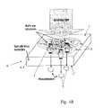
- FIG. 4Bis a shematical perspective view of an apparatus for separating and characterising an electromagnetic radiation (light) incorporating a device as shown on FIG. 4A .
- FIG. 6is a graph showing the measured strength of each transmission peak for a combination of three concentrator structures with different periodicities fabricated in a 300 nm thick silver film when they have an overlap of 50% (d7) and when the spacing is larger so that there is no overlap (d15).
- the overlapis defined here as the fraction of the area of one bull's eye overlapping with one or more of the neighbouring structures.
- the strength of the transmission peaksdecreases much less than the amount of overlap. This shows that even for light incident on the overlap area, optical energy is being preferentially concentrated at different apertures depending on wavelength.
- FIG. 7is a perspective top view of a device according to an other embodiment of the invention, comprising an array of partially overlapped groups of concentrator structures fabricated in a gold film, each with three bull's eye structures of different wavelength. Overlapping concentrator arrays such as this may be used to perform spectral or polarimetric imaging.
- FIG. 8is a partial perspective top view of a device according to an other embodiment of the invention, adapted for polarimetric imaging.
- An array of slitsis fabricated in a metal film with corresponding corrugations. The slits will receive optical energy from the neighbouring set of parallel corrugations with a strength dependent on the polarization of the incident light.
- Individual light sensor elementsplaced under each of the slits record signals which may be used to construct a polarimetric image.
- a key characteristic of the inventionis that electromagnetic radiation, for example light, containing different spectral and/or polarization components impinging on the overlapping area can be separated laterally by the inventive device, according to the properties of the different components.
- the energy in the different componentsis preferentially concentrated in different locations.
- Such decompositionis a basic building block enabling, among others, spectroscopic and polarimetric sensing.
- the surface overlapping ratecan be from several tens of percent (for example: 30%, 50%, 70%) up to 100% (cf. FIG. 8 ).
- each structurewill collect a different spectral component of the light incident on the overlap area.
- the overlap areamay extend over most, or all, of the area occupied by the combined structure.
- a light sensormay be placed under each aperture to collect information on the spectral content of light incident on the combined light concentrator structures, as indicated in FIG. 3A . Even if the light sensors are laterally separated, the overlapping light collection structures enable both light sensors to efficiently collect light from most, or all, of the area occupied by the combined structure.
- the basic principle just describedcan be extended to more spectral components, or polarization components, by increasing the number of overlapping concentrator structures.
- FIG. 4AThis is illustrated in FIG. 4A for a triple light collecting device.
- the three bull's eye structureshave different periods in order to collect three different spectral components of the incident light.
- An analogous scheme for characterizing polarizationwill be described below.
- the results shown in FIG. 5demonstrate how such overlapping structures can separate components of the light incident on the overlap area and bring the optical energy to the respective apertures at the center of each structure.
- the light transmitted by the apertures of two bull's eye structures with different periodsis compared when they are far apart and when the center-to-center distances are 7 um. The latter case corresponds to an overlap of about 30%.
- the light collector structuresare far apart, they have a transmission peak defined mainly by their period.
- each aperturestill has a distinct spectrum dominated by the spectral characteristics of the isolated bull's eye structure.
- the said assemblyBy analyzing light impinging on a localized area, the said assembly performs the functions needed to collect the signals corresponding to one pixel of a spectral and/or polarimetric image. It will therefore be referred to such an assembly as a “superpixel” hereinafter.
- the collected output of the light sensors in all superpixelswill constitute a spectral and/or polarimetric image.
- the resulting spectral imaging systemwill exhibit better spectral registration between bands and has potential to make more efficient use of the light, compared to an imaging system based on Bayer mask filters or similar.
- optical energyis concentrated in a small area, potentially smaller than the free-space wavelength of light, even if the light sensitive area of the superpixel unit is significantly larger.
- One way to derive polarimetric informationis to use overlapping structures of the type shown in FIG. 2 , oriented in different directions.
- the structure shown in FIG. 8combines different polarization dependent light collecting structures that overlap in a triangular lattice.
- each edge of a given triangleis a slit aperture collecting light from the neighbouring set of corrugations parallel to the slit.
- the light transmitted by the apertures described abovenormally diffracts as it emerges on the opposite side of the film. It is known (see for example Lezec et al., Science vol 297, p. 820, 2002, Martin-Moreno et al., Phys. Rev. Lett. vol. 90, 167401, 2003 and U.S. Pat. No. 7,057,151) that the diffraction at the exit of the aperture can be controlled by structuring the surrounding output surface of said aperture.
- the emerging lightcan be focused and beamed either normal to the surface or with an oblique angle.
- the structuring on the output sidemay consist of combined or overlapping structures for focusing or beaming different components of light in different directions. In this manner it is possible to further separate the light on the output side, for example by directing different polarizations onto different light sensor elements.
- An important general aspect of the inventionis the use of spatially overlapping, or superposed, plasmonic structures capable of separately concentrating the optical energy of components of light with different characteristics such as wavelength, polarization, angle of incidence or combinations thereof.
- any number of plasmonic concentrator structuresmay be combined in this way, and the overlap may be partial or complete.
- the overlappingmay be accomplished in many ways depending on performance requirements and fabrication capabilities.
- one way to use the said overlapping light-concentrating structuresis to couple light sensors to each of the overlapping concentrator structures in order to measure the strength of the separated components of light.
- the overlapping concentrator structuresin reverse to combine light from different sources, with the output light having properties such that it appears to come from a single source.
- another aspect of the inventionis that it is possible to use the overlapping plasmonic structures to generate, or display, an image by replacing light sensors with light sources. This could find use in image projectors or displays.
- the periodic structurescan be made of grooves or protruding structures on the metal film.
- the periodic structurescan be made of metal or dielectric material.
- the preferred metaldepends on the properties of the metal at the wavelength of interest. In the visible range, silver is the preferred metal while in the infra-red gold is also very good.
- the central aperturemay have a variety of shapes and may be smaller or larger than the wavelength.
- the boundaries between superpixelsmay be delineated in various ways to define the sensitive area of the superpixel. This may include truncating individual concentrator structures at boundary lines between superpixels, as well as means to control the propagation of charge oscillations across the superpixel boundaries.
- spectral imagingis used to refer to imaging techniques which resolve incoming light not only spatially, but also spectrally. This includes “multispectral imaging”, which normally refers to systems with 2 to 10 different spectral channels, as well as “hyperspectral imaging” which normally refers to systems with tens or hundreds of spectral channels.)
- a typical spectral imaging systemforms an image consisting of individual pixels, and for each pixel information is recorded about the wavelength distribution of the incoming light.
- the most common form of spectral imagingis color imaging, which images visible light separated into three spectral channels corresponding to the primary colours of the human eye.
- the same dispositions and features, including polarization-dependent structurescan be extended to other wavelengths such as thermal and microwave regions essentially by scaling the structures and choosing appropriate light sensors (or sources).
- One possible applicationis spectral or polarimetric imaging at thermal infrared wavelengths, which can be of interest in military applications. At longer wavelengths, fabrication is facilitated by the larger dimensions of the concentrator structures. In general, many other applications will be apparent to those skilled in the respective application areas.
- a single “superpixel” as discussed abovemay be used as a highly compact spectrometer device suitable, among other things, for coupling to an optical fiber or inclusion in microsystems.
Landscapes
- Physics & Mathematics (AREA)
- Spectroscopy & Molecular Physics (AREA)
- General Physics & Mathematics (AREA)
- Chemical & Material Sciences (AREA)
- Engineering & Computer Science (AREA)
- Optics & Photonics (AREA)
- Life Sciences & Earth Sciences (AREA)
- Nanotechnology (AREA)
- Pathology (AREA)
- Immunology (AREA)
- General Health & Medical Sciences (AREA)
- Biochemistry (AREA)
- Analytical Chemistry (AREA)
- Health & Medical Sciences (AREA)
- Crystallography & Structural Chemistry (AREA)
- Biophysics (AREA)
- Microelectronics & Electronic Packaging (AREA)
- Investigating Or Analysing Materials By Optical Means (AREA)
- Silicon Compounds (AREA)
- Photometry And Measurement Of Optical Pulse Characteristics (AREA)
- Investigating, Analyzing Materials By Fluorescence Or Luminescence (AREA)
- Spectrometry And Color Measurement (AREA)
Abstract
Description
- The present invention is related to the field of treatment of electromagnetic energy, in particular of optical energy, more specifically in the infrared and visible wavelengths, and concerns a device for sorting and concentrating electromagnetic energy of radiations with different properties, as well as an apparatus comprising at least one such device.
- Even though the present invention is more specifically described in relation to visible light or infrared radiations, it should be understood that a much wider range or types of electromagnetic radiations can be impacted by this invention, more specifically radiations ranging in matter of wavelength from microwaves to ultraviolet radiations.
- In particular, in a wide variety of optical sensing applications, there is a need for devices able to characterize the spectrum (i.e. wavelength distribution) of incoming radiation (light). There are also applications which require characterization of the polarization state of the radiation or light. Almost invariably in these applications, there is a need to make efficient use of the available light while preserving signal integrity. This is normally combined with constraints on device size and/or cost.
- Current imaging technology is based on arrays of light sensors, for example arrays based on silicon CCD or CMOS technology. In a basic imaging system using a two-dimensional matrix array of light sensors, the signal from each sensor element corresponds to one pixel in the image.
- Spectral and polarometric imaging faces a general technological challenge in that the image data are essentially three-dimensional (with spectral or polarimetric information constituting a third dimension) while light sensor arrays generally are limited to two dimensions.
- For color imaging, it is common to use a matrix array of light sensors equipped with individual color filters, each passing one of the primary colors, arranged in a so-called “Bayer pattern” or similar.
- In this case, the partial images corresponding to each primary colour are not spatially registered, and some form of interpolation is needed to estimate, for each pixel, the amount of light in the two primary colours not passed by the spectral filter of the corresponding light sensor element. This can lead to color artefacts in the resulting image.
- Also, each light sensor element collects only light within its own spectral band, and thereby the rest of the light impinging on that particular element is lost.
- There is a general demand to overcome the limitations exposed herein before, for applications in connection with the handling, treatment and/or exploitation of visible light, as well as other electromagnetic radiations having longer or shorter wavelengths.
- On the other hand, there has been, in recent years, significant progress in the understanding and exploitation of charge oscillation phenomena at optical frequencies on metal surfaces, a field known as plasmonics [see for example: Barnes et al.,Naturevol. 424, p. 824, 2003; C. Genet and T. W. Ebbesen,Naturevol. 445 p. 39 (2007)].
- Indeed, surface plasmons (SPs) have generated considerable interest recently due to their potential in optics and sensing, among numerous other applications [see for example: Zayats, A. V., Smolyaninov, I. I & Maradudin, A. A. “Nano-optics of surface plasmon polaritons.”Phys. Rep.408, 131-314 (2005) ; Mikhailov, V., Wurtz, G., Elliot, J., Bayvel, P., Zayats, A. V. “Dispersing Light with Surface Plasmon Polaritonic Crystals.”Phys. Rev. Lett.99, 083901 (2007); Zia, R., Schuller, J. A., Chandran, A., Brongersma, M. L. “Plasmonics: the next chip-scale technology.”Materials Today.9, 20-27 (2006)].
- Surface plasmons are essentially light waves trapped at a metal surface by their interaction with the free electrons in the metal. Their properties can be controlled by texturing the metal surface. In the context of spectral and polarizing imaging, single apertures surrounded by periodic grooves are of particular interest [see for example: Thio, T., Pellerin, K. M., Linke, R. A., Lezec, H. J. & Ebbesen, T. W. “Enhanced light transmission through a single subwavelength aperture.”Opt. Lett.26, 1972-1974 (2001); Nahata, A., Linke, R. A., Ishi, T. & Ohashi, K. “Enhanced nonlinear optical conversion from a periodically nanostructured metal film.”Opt. Lett.28, 423-425 (2003); Garcia-Vidal, F. J., Lezec, H. J., Ebbesen, T. W. & Martin-Moreno, L. “Multiple paths to enhance optical transmission through a subwavelength slit.”Phys. Rev. Lett.90, 213901 (2003)].
- The periodic grooves act like an antenna for the incoming light by converting it to surface plasmons and enhancing the transmission through the aperture.
FIG. 1 gives an example of one such aperture structure where a single subwavelength hole is surrounded by concentric grooves.- Such a structure, also known as “bull's eye” structure can, for example, be milled by focused ion beam (FIB) lithography in the surface of a metal film (for example made of silver or gold). Such a device may be for visible light for example a 300 nm thick Ag film on a glass substrate with a structure having the following dimensions: diameter of central hole: 170 nm; width of grooves: 150 nm; depths of grooves: between 10 nm and 150 nm; spatial period: 600 nm.
- As indicated by the arrows, incident light excites surface charge oscillations, and the optical energy is concentrated at the center of the structure where it enters an aperture in the film. The light emerges at the back side of the film where, depending on the structuring of the back side, the light may diffract out as indicated. The structure preferentially collects light within a band of wavelengths determined mainly by the period of the ring structure. At the bottom is an image of an actual bull's eye structure fabricated in a gold film.
- The transmission peak wavelength λSPPof such a structure can be tuned by controlling the groove periodicity P (
FIG. 1 b) as predicted by equation (1) for normal incidence illumination: - where εmand εdare the dielectric constants of the metal and the dielectric in immediate contact with the metal surface. The peak is normally red-shifted compared to the prediction of equation (1) due to Fano-type interaction. The transmission spectrum is also modulated by the other structural parameters such as groove depth, width, aperture shape and size, as indicated in the previously quoted references.
- Such a structure preferentially collects optical energy within a band of wavelengths adapted to its period.
- The surface plasmons give rise to intense electromagnetic fields at the central hole. The flux per unit area through the aperture can be larger than that of the incident light, confirming that the grooves act as an antenna, collecting light laterally from an area around the hole. This extraordinary transmission phenomenon allows for useful light collection efficiencies even though the apertures represent only a small fraction of the surface of the device, the optical energy being extracted at the back of the film, at the exit opening of the aperture, after passing through the latter.
- Another example of a known radiation or light concentrating structure consists of a metal film with linear corrugations surrounding a slit-shaped aperture in which the optical or radiative energy is concentrated, as illustrated in
FIG. 2 . The concentrating effect of this structure depends not only on the wavelength, but also on the polarization of the incoming light or radiation. - Now, the inventors have discovered unexpectedly that plasmonics based surface collector structures can be applied to realise at least a spectrally differentiated or polarisation selective collection, and therefore a characterisation of the spectral properties, of electromagnetic radiations, and in particular of light, which allows in particular to overcome the above mentioned limitations in respect of the known Bayer-mask technique.
- Thus, according to the invention there is proposed a device for sorting and collecting electromagnetic energy impinging a surface of said device, said surface comprising at least one plasmonics-based surface structure or a similar surface structure having one or more specific resonance(s), characterised in that said surface is provided with at least two such surface structures, acting as individual collector structures, which are at least partially spatially overlapped or superposed.
- This inventive basic concept allows, depending on the design and layout of each of the intermeshed individual surface structures, to sort out and to concentrate radiation components having different specific properties, the overlapped areas acting surprisingly without noticeable mutual interference.
- Advantageous embodiments or additional features of the device according to the invention are exposed in
claims 2 to22. - Such a device can in particular be used to perform spectroscopy or polarimetry.
- The present invention also concerns an apparatus for separating and characterising an electromagnetic radiation impinging the surface(s) of at least one thin plate or film like body, characterised in that said body or each of said bodies consists of a device as described before, wherein each radiation component sorted by one of the concentrator structures is concentrated at an entry opening of a corresponding aperture and wherein a sensor or a group of sensors is arranged on the side of the body opposite the impinging surface to collect information of the separated radiation components emanating from the exit opening(s) of one or several apertures.
- Such an apparatus can for example be used to perform spectral and/or polarimetric imaging, as well as colour imaging.
- An application of that kind is for example described in: “Plasmonic photon sorters for spectral and polarimetric imaging”, E. Laux et al., Nature Photonics, Vol. 2, 161-164 (2008).
- The present invention further concerns an apparatus for combining electromagnetic radiations having different properties and delivered by different sources into a single electromagnetic radiation, characterised in that it comprises at least one device as described before, wherein the radiation emitted by each source is fed into a corresponding aperture of said body through its exit opening, said different radiations being combined as constitutive components into a single radiation emitted from the surface provided with the concentrator structures.
- Such an apparatus can for example be used to perform image display or projection.
- Other objects of the present invention are mentioned in the enclosed claims and will become more readily apparent in light of the following description in conjunction with the following accompanying drawings, wherein:
FIG. 3A is a cross-sectional perspective view of an apparatus for separating and characterising an electromagnetic radiation, in particular light, which incorporates a device according to a first embodiment of the invention. This embodiment of the device consists of two overlapping bull's eye concentrator structures, concentrating different spectral components of the incoming light. Two light sensor elements are placed underneath the metal film according to the invention, receiving the optical energy concentrated by each of the bull's eyes structure. Such an assembly may be used to collect signals containing information about the spectral distribution of incoming light.FIG. 3B is a top view of an embodiment similar toFIG. 3A made of a pair of overlapping bull's eye structures fabricated in the surface of a gold film according to the invention.FIG. 4A is a top view of a device according to a second embodiment of the invention. This embodiment consists of three partially overlapping bull's eye concentrator structures fabricated in the surface of a gold film. Each concentrator structure has a different periodicity of the rings. Thus, the structures preferentially concentrate three different spectral components of the incident light.FIG. 4B is a shematical perspective view of an apparatus for separating and characterising an electromagnetic radiation (light) incorporating a device as shown onFIG. 4A .FIG. 5 is a graph showing the measured total transmission spectra of three different double concentrator structures similar to the one shown inFIG. 3 , each with different separation of the two central holes. The structures are fabricated in a 300 nm thick silver film. Each bull's eye structure has a radius of about 7 micrometers. The figure shows measurements for center-to-center spacings of 7, 11 and 15 micrometers. It can be clearly seen that the position of the main transmission peaks remains essentially unaffected by the degree of overlap between the two concentrators which is about 30% in the case of 7 micrometer spacing.FIG. 6 is a graph showing the measured strength of each transmission peak for a combination of three concentrator structures with different periodicities fabricated in a 300 nm thick silver film when they have an overlap of 50% (d7) and when the spacing is larger so that there is no overlap (d15). The overlap is defined here as the fraction of the area of one bull's eye overlapping with one or more of the neighbouring structures. The strength of the transmission peaks decreases much less than the amount of overlap. This shows that even for light incident on the overlap area, optical energy is being preferentially concentrated at different apertures depending on wavelength.FIG. 7 is a perspective top view of a device according to an other embodiment of the invention, comprising an array of partially overlapped groups of concentrator structures fabricated in a gold film, each with three bull's eye structures of different wavelength. Overlapping concentrator arrays such as this may be used to perform spectral or polarimetric imaging.FIG. 8 is a partial perspective top view of a device according to an other embodiment of the invention, adapted for polarimetric imaging. An array of slits is fabricated in a metal film with corresponding corrugations. The slits will receive optical energy from the neighbouring set of parallel corrugations with a strength dependent on the polarization of the incident light. Individual light sensor elements (not shown) placed under each of the slits record signals which may be used to construct a polarimetric image.FIG. 9 is a schematical cross-sectional view of a device according to an other embodiment of the invention, similar to the one shown onFIG. 3 but also provided with concentrator structures on its exiting surface.- Central to this invention is the use of overlapping, or superposed, plasmonic collector structures, such as those in
FIGS. 1 and 2 , to collect and to concentrate different wavelengths or polarizations at separate locations. - Indeed, a key characteristic of the invention is that electromagnetic radiation, for example light, containing different spectral and/or polarization components impinging on the overlapping area can be separated laterally by the inventive device, according to the properties of the different components. The energy in the different components is preferentially concentrated in different locations. Such decomposition is a basic building block enabling, among others, spectroscopic and polarimetric sensing.
- The surface overlapping rate can be from several tens of percent (for example: 30%, 50%, 70%) up to 100% (cf.
FIG. 8 ). - This is exemplified by the pair of overlapping bull's eye structures with different periods milled in a gold film, shown in
FIG. 3 . Here light impinging on one of the structures, with a wavelength matching the period of that structure, will be preferentially concentrated at the center of that structure. This is the case even for light incident on the overlap area. Thus, each structure will collect a different spectral component of the light incident on the overlap area. Depending on the center to center distance and the layout of the light concentrating structures fabricated according to the invention, the overlap area may extend over most, or all, of the area occupied by the combined structure. - According to the invention, a light sensor may be placed under each aperture to collect information on the spectral content of light incident on the combined light concentrator structures, as indicated in
FIG. 3A . Even if the light sensors are laterally separated, the overlapping light collection structures enable both light sensors to efficiently collect light from most, or all, of the area occupied by the combined structure. - According to the invention, the basic principle just described can be extended to more spectral components, or polarization components, by increasing the number of overlapping concentrator structures.
- This is illustrated in
FIG. 4A for a triple light collecting device. Here the three bull's eye structures have different periods in order to collect three different spectral components of the incident light. An analogous scheme for characterizing polarization will be described below. - The results shown in
FIG. 5 demonstrate how such overlapping structures can separate components of the light incident on the overlap area and bring the optical energy to the respective apertures at the center of each structure. In the figure, the light transmitted by the apertures of two bull's eye structures with different periods is compared when they are far apart and when the center-to-center distances are 7 um. The latter case corresponds to an overlap of about 30%. When the light collector structures are far apart, they have a transmission peak defined mainly by their period. In the overlapped structure, each aperture still has a distinct spectrum dominated by the spectral characteristics of the isolated bull's eye structure. - If the transmission at the three preferential wavelengths defined by the three periods is plotted as a function of overlap between the three structures, one notices that the overlap introduces very little loss relative to the isolated structures as shown in
FIG. 6 . This result further confirms the ability of the overlapping concentrators to laterally separate light impinging on the overlap area, in this case a separation according to wavelength. This provides a clear proof of concept of the invention. - An assembly of light concentrator structures and light sensors according to the invention can be used to characterize the spectral and/or polarimetric properties of light impinging on a localized area defined by the light concentrator structures. Such an assembly in itself can have important applications such as highly compact spectrometers.
- By analyzing light impinging on a localized area, the said assembly performs the functions needed to collect the signals corresponding to one pixel of a spectral and/or polarimetric image. It will therefore be referred to such an assembly as a “superpixel” hereinafter.
- According to the invention, it is possible to fabricate an array of multiple superpixel units, for example by arranging the light concentrator structures as shown in
FIG. 7 . - By placing such an array of superpixels at the focus of suitable imaging optics, the collected output of the light sensors in all superpixels will constitute a spectral and/or polarimetric image. The resulting spectral imaging system will exhibit better spectral registration between bands and has potential to make more efficient use of the light, compared to an imaging system based on Bayer mask filters or similar.
- An important aspect of the invention is that the optical energy is concentrated in a small area, potentially smaller than the free-space wavelength of light, even if the light sensitive area of the superpixel unit is significantly larger.
- This enables the use of very small light sensor elements, typically fabricated as a monolithic array on a semiconductor chip.
- Use of small light sensor elements according to the invention is advantageous in several ways including the following:
- Firstly, this enables the use of more closely spaced light sensor elements compared to “Bayer mask” or similar technologies, with a resulting potential to reduce the total area required for the light sensor array.
- Secondly, the size of the light sensor elements is an important factor determining their speed of response (see for instance T. Ishi et al., Jpn. J. Appl. Phys. vol. 44 p. L364 (2005)).
- Thirdly, the size of the light sensor element may also determine the strength of important contributions to sensor noise, depending on the sensor technology.
- A fourth advantage is that the use of plasmonic light concentrators avoids the need for a light sensor array with a high ratio of light sensitive area to total area, known as “fill factor”. A reduced requirement on fill factor may provide opportunity to increase the functionality of the chip carrying the light sensor array, or it may be translated into cost savings on the light sensor array fabrication.
- Hereinafter, it will be outlined in more detail how the invention may be used to characterize the polarization state of light, including polarimetric imaging.
- One way to derive polarimetric information is to use overlapping structures of the type shown in
FIG. 2 , oriented in different directions. - For instance, the structure shown in
FIG. 8 combines different polarization dependent light collecting structures that overlap in a triangular lattice. - In this complex structure, each edge of a given triangle is a slit aperture collecting light from the neighbouring set of corrugations parallel to the slit. By placing photodetectors below each slit, it is possible to record polarimetric information of the incident light and, in conjunction with suitable imaging optics, to form a polarimetric image.
- The light transmitted by the apertures described above normally diffracts as it emerges on the opposite side of the film. It is known (see for example Lezec et al., Science vol 297, p. 820, 2002, Martin-Moreno et al., Phys. Rev. Lett. vol. 90, 167401, 2003 and U.S. Pat. No. 7,057,151) that the diffraction at the exit of the aperture can be controlled by structuring the surrounding output surface of said aperture.
- By the appropriate choice of structuring, the emerging light can be focused and beamed either normal to the surface or with an oblique angle. According to the invention, the structuring on the output side may consist of combined or overlapping structures for focusing or beaming different components of light in different directions. In this manner it is possible to further separate the light on the output side, for example by directing different polarizations onto different light sensor elements.
- An important general aspect of the invention is the use of spatially overlapping, or superposed, plasmonic structures capable of separately concentrating the optical energy of components of light with different characteristics such as wavelength, polarization, angle of incidence or combinations thereof. According to the invention, any number of plasmonic concentrator structures may be combined in this way, and the overlap may be partial or complete. The overlapping may be accomplished in many ways depending on performance requirements and fabrication capabilities.
- According to the invention, one way to use the said overlapping light-concentrating structures is to couple light sensors to each of the overlapping concentrator structures in order to measure the strength of the separated components of light.
- According to the invention, it is also possible to use the overlapping concentrator structures in reverse to combine light from different sources, with the output light having properties such that it appears to come from a single source. Thus, another aspect of the invention is that it is possible to use the overlapping plasmonic structures to generate, or display, an image by replacing light sensors with light sources. This could find use in image projectors or displays.
- Many alternative embodiments of the invention will be apparent to those skilled in the art. For instance, the periodic structures can be made of grooves or protruding structures on the metal film. The periodic structures can be made of metal or dielectric material. The preferred metal depends on the properties of the metal at the wavelength of interest. In the visible range, silver is the preferred metal while in the infra-red gold is also very good. The central aperture may have a variety of shapes and may be smaller or larger than the wavelength. The boundaries between superpixels may be delineated in various ways to define the sensitive area of the superpixel. This may include truncating individual concentrator structures at boundary lines between superpixels, as well as means to control the propagation of charge oscillations across the superpixel boundaries.
- An important class of relevant applications of the invention is spectral imaging. (Here the term “spectral imaging” is used to refer to imaging techniques which resolve incoming light not only spatially, but also spectrally. This includes “multispectral imaging”, which normally refers to systems with 2 to 10 different spectral channels, as well as “hyperspectral imaging” which normally refers to systems with tens or hundreds of spectral channels.) A typical spectral imaging system forms an image consisting of individual pixels, and for each pixel information is recorded about the wavelength distribution of the incoming light. The most common form of spectral imaging is color imaging, which images visible light separated into three spectral channels corresponding to the primary colours of the human eye. It is well known that this colour information strongly increases the information content of the image compared to the case of monochrome imaging (“black and white”, no spectral information). Furthermore, it is a well established fact that the addition of more spectral channels, such as in hyperspectral imaging, adds significant extra information which greatly facilitates automated computer analysis of the images.
- In addition to its spectral distribution, an incoming light signal is also characterized by its polarization state, which often carries valuable information. In analogy with spectral imaging, polarimetric imaging refers to techniques that form images in a way which is sensitive to polarization state. It is known that applications ranging from surface inspection to military target detection may benefit from measurement of polarization state, for example through polarimetric imaging.
- In the foregoing specification, illustrated by the enclosed drawings, the invention has been mainly described in view of applications related to visible light.
- However, according to the invention, the same dispositions and features, including polarization-dependent structures, can be extended to other wavelengths such as thermal and microwave regions essentially by scaling the structures and choosing appropriate light sensors (or sources). One possible application is spectral or polarimetric imaging at thermal infrared wavelengths, which can be of interest in military applications. At longer wavelengths, fabrication is facilitated by the larger dimensions of the concentrator structures. In general, many other applications will be apparent to those skilled in the respective application areas. For example, a single “superpixel” as discussed above may be used as a highly compact spectrometer device suitable, among other things, for coupling to an optical fiber or inclusion in microsystems.
- The following non limitative numerical references appear in the appending drawings and claims:
- 1: device
- 1′: impringed surface
- 1″: exited surface
- 2: individual surface structure
- 3: aperture/localised region of energy concentration
- 4: plate or film-like body
- 5: group of overlapping surface structures
- 6: apparatus
- 7: sensors
- While there has been described and illustrated various embodiments of the invention, it will be apparent to those skilled in the art that variations and modifications are possible without deviating from the spirit and broad teachings of the invention which shall be limited solely by the scope of the claims appended hereto.
Claims (23)
Priority Applications (1)
| Application Number | Priority Date | Filing Date | Title |
|---|---|---|---|
| US12/532,499US8174696B2 (en) | 2007-03-22 | 2008-03-25 | Device for sorting and concentrating electromagnetic energy and apparatus comprising at least one such device |
Applications Claiming Priority (3)
| Application Number | Priority Date | Filing Date | Title |
|---|---|---|---|
| US90713607P | 2007-03-22 | 2007-03-22 | |
| US12/532,499US8174696B2 (en) | 2007-03-22 | 2008-03-25 | Device for sorting and concentrating electromagnetic energy and apparatus comprising at least one such device |
| PCT/IB2008/001285WO2008114148A2 (en) | 2007-03-22 | 2008-03-25 | Device for sorting and concentrating electromagnetic energy and apparatus comprising at least one such device |
Publications (2)
| Publication Number | Publication Date |
|---|---|
| US20100110430A1true US20100110430A1 (en) | 2010-05-06 |
| US8174696B2 US8174696B2 (en) | 2012-05-08 |
Family
ID=39766559
Family Applications (1)
| Application Number | Title | Priority Date | Filing Date |
|---|---|---|---|
| US12/532,499Expired - Fee RelatedUS8174696B2 (en) | 2007-03-22 | 2008-03-25 | Device for sorting and concentrating electromagnetic energy and apparatus comprising at least one such device |
Country Status (5)
| Country | Link |
|---|---|
| US (1) | US8174696B2 (en) |
| EP (1) | EP2132556B1 (en) |
| JP (1) | JP2010524012A (en) |
| AT (1) | ATE509265T1 (en) |
| WO (1) | WO2008114148A2 (en) |
Cited By (19)
| Publication number | Priority date | Publication date | Assignee | Title |
|---|---|---|---|---|
| US20090108203A1 (en)* | 2007-10-31 | 2009-04-30 | Gregoire Daniel J | Multiple-band detector using frequency selective slots |
| US20100226134A1 (en)* | 2007-11-19 | 2010-09-09 | President And Fellows Of Harvard College | Methods and Apparatus for Improving Collimation of Radiation Beams |
| EP2738579A1 (en)* | 2012-11-30 | 2014-06-04 | Samsung Electronics Co., Ltd | Optical switch and optical logic device |
| US20140294043A1 (en)* | 2012-11-30 | 2014-10-02 | Robert Bosch Gmbh | Mems infrared sensor including a plasmonic lens |
| KR20150050093A (en)* | 2013-10-31 | 2015-05-08 | 삼성전자주식회사 | Apparatus of outputting directional light and light interconnection system having the same |
| US20150228827A1 (en)* | 2014-02-13 | 2015-08-13 | Palo Alto Research Center Incorporated | Solar Power Harvesting System With Metamaterial Enhanced Solar Thermophotovoltaic Converter (MESTC) |
| US20150228844A1 (en)* | 2014-02-13 | 2015-08-13 | Palo Alto Research Center Incorporated | Spectrally-Selective Metamaterial Emitter |
| TWI506270B (en)* | 2010-05-13 | 2015-11-01 | Seiko Epson Corp | Optical device and analyzing apparatus |
| US20160254396A1 (en)* | 2014-02-13 | 2016-09-01 | Palo Alto Research Center Incorporated | Metamaterial Enhanced Thermophotovoltaic Converter |
| WO2018195518A1 (en)* | 2017-04-21 | 2018-10-25 | Trustees Of Boston University | Azimuthally-modulated aperiodic phase arrays for engineered spectral separation |
| CN108802038A (en)* | 2018-08-28 | 2018-11-13 | 京东方科技集团股份有限公司 | Light source assembly and micro-total analysis system |
| EP3462218A1 (en)* | 2014-01-27 | 2019-04-03 | Forelux Inc. | Photonic apparatus with periodic structures |
| US10288323B2 (en) | 2015-12-15 | 2019-05-14 | Palo Alto Research Center Incorporated | Solar receiver with metamaterials-enhanced solar light absorbing structure |
| US10677965B2 (en) | 2014-01-27 | 2020-06-09 | Forelux Inc. | Optical apparatus for non-visible light applications |
| US11579456B2 (en) | 2017-08-31 | 2023-02-14 | Metalenz, Inc. | Transmissive metasurface lens integration |
| US11733535B2 (en) | 2014-12-10 | 2023-08-22 | President And Fellows Of Harvard College | Achromatic metasurface optical components by dispersive phase compensation |
| US11927769B2 (en) | 2022-03-31 | 2024-03-12 | Metalenz, Inc. | Polarization sorting metasurface microlens array device |
| US11978752B2 (en) | 2019-07-26 | 2024-05-07 | Metalenz, Inc. | Aperture-metasurface and hybrid refractive-metasurface imaging systems |
| US12140778B2 (en) | 2018-07-02 | 2024-11-12 | Metalenz, Inc. | Metasurfaces for laser speckle reduction |
Families Citing this family (18)
| Publication number | Priority date | Publication date | Assignee | Title |
|---|---|---|---|---|
| JP5273932B2 (en)* | 2007-03-23 | 2013-08-28 | キヤノン株式会社 | Photodetection element, photodetection method, imaging element, and imaging method |
| US7923689B2 (en)* | 2009-04-30 | 2011-04-12 | Raytheon Company | Multi-band sub-wavelength IR detector having frequency selective slots and method of making the same |
| US9356224B2 (en)* | 2009-10-30 | 2016-05-31 | The Regents Of The University Of California | Thin film bismuth iron oxides useful for piezoelectric devices |
| EP2938979B1 (en)* | 2012-12-22 | 2024-03-27 | Robert Bosch GmbH | Mems infrared sensor including a plasmonic lens |
| CA2930836A1 (en) | 2013-11-17 | 2015-05-21 | Quantum-Si Incorporated | Active-source-pixel, integrated device for rapid analysis of biological and chemical specimens |
| WO2016023010A1 (en) | 2014-08-08 | 2016-02-11 | Quantum-Si Incorporated | Optical system and assay chip for probing, detecting, and analyzing molecules |
| US10174363B2 (en) | 2015-05-20 | 2019-01-08 | Quantum-Si Incorporated | Methods for nucleic acid sequencing |
| MX384725B (en) | 2014-08-08 | 2025-03-14 | Quantum Si Inc | INTEGRATED DEVICE WITH EXTERNAL LIGHT SOURCE FOR PROBING, DETECTION AND ANALYSIS OF MOLECULES. |
| BR112017002485B1 (en) | 2014-08-08 | 2020-12-01 | Quantum-Si Incorporated | integrated circuit and photodetection method |
| WO2017088014A1 (en)* | 2015-11-24 | 2017-06-01 | Nanyang Technological University | Plasmonic structure for distinguishing light polarisation and method |
| FR3044466A1 (en)* | 2015-12-01 | 2017-06-02 | Commissariat Energie Atomique | IMAGE SENSOR WITH SPECTRAL SORTING DEVICE |
| EP3402903B1 (en) | 2016-01-15 | 2022-03-02 | Quantapore, Inc. | Optically-based nanopore analysis with reduced background |
| KR102120134B1 (en)* | 2016-01-26 | 2020-06-09 | 한국전자통신연구원 | Resonator and optical sensor using thereof |
| KR20180111999A (en) | 2016-02-17 | 2018-10-11 | 테서렉트 헬스, 인코포레이티드 | Sensors and devices for life-time imaging and detection applications |
| JP2018004694A (en)* | 2016-06-27 | 2018-01-11 | 国立大学法人静岡大学 | Optical element, image pick-up device including the same, and manufacturing method of optical element and image pick-up device |
| BR112019012540A2 (en) | 2016-12-22 | 2019-11-12 | Quantum-Si Incorporated | direct-pack pixel integrated photodetector |
| US12078596B2 (en) | 2017-07-24 | 2024-09-03 | Quantum-Si Incorporated | Hand-held, massively-parallel, bio-optoelectronic instrument |
| BR112020024790A2 (en) | 2018-06-22 | 2021-03-02 | Quantum-Si Incorporated | integrated photodetector with load storage region of varying detection time |
Citations (5)
| Publication number | Priority date | Publication date | Assignee | Title |
|---|---|---|---|---|
| US20030103150A1 (en)* | 2001-11-30 | 2003-06-05 | Catrysse Peter B. | Integrated color pixel ( ICP ) |
| US20040046128A1 (en)* | 1999-06-05 | 2004-03-11 | Andreas Peter Abel | Sensor platform and method for the determination of multiple analytes |
| US20050110990A1 (en)* | 2003-10-17 | 2005-05-26 | Tae-Woong Koo | Method and device for detecting small numbers of molecules using surface-enhanced coherent anti-Stokes Raman spectroscopy |
| US20050161589A1 (en)* | 2003-12-05 | 2005-07-28 | University Of Pittsburgh | Metallic nano-optic lenses and beam shaping devices |
| US20080174509A1 (en)* | 2006-12-27 | 2008-07-24 | Williams Brett A | Subwavelength Aperture Monopulse Conformal Antenna |
Family Cites Families (2)
| Publication number | Priority date | Publication date | Assignee | Title |
|---|---|---|---|---|
| US7057151B2 (en)* | 2001-08-31 | 2006-06-06 | Universite Louis Pasteur | Optical transmission apparatus with directionality and divergence control |
| US6700712B2 (en)* | 2001-11-13 | 2004-03-02 | 3M Innovative Properties Company | Multidirectional single surface optically shaped film |
- 2008
- 2008-03-25ATAT08776261Tpatent/ATE509265T1/ennot_activeIP Right Cessation
- 2008-03-25EPEP08776261Apatent/EP2132556B1/ennot_activeNot-in-force
- 2008-03-25USUS12/532,499patent/US8174696B2/ennot_activeExpired - Fee Related
- 2008-03-25JPJP2010500384Apatent/JP2010524012A/ennot_activeWithdrawn
- 2008-03-25WOPCT/IB2008/001285patent/WO2008114148A2/enactiveApplication Filing
Patent Citations (5)
| Publication number | Priority date | Publication date | Assignee | Title |
|---|---|---|---|---|
| US20040046128A1 (en)* | 1999-06-05 | 2004-03-11 | Andreas Peter Abel | Sensor platform and method for the determination of multiple analytes |
| US20030103150A1 (en)* | 2001-11-30 | 2003-06-05 | Catrysse Peter B. | Integrated color pixel ( ICP ) |
| US20050110990A1 (en)* | 2003-10-17 | 2005-05-26 | Tae-Woong Koo | Method and device for detecting small numbers of molecules using surface-enhanced coherent anti-Stokes Raman spectroscopy |
| US20050161589A1 (en)* | 2003-12-05 | 2005-07-28 | University Of Pittsburgh | Metallic nano-optic lenses and beam shaping devices |
| US20080174509A1 (en)* | 2006-12-27 | 2008-07-24 | Williams Brett A | Subwavelength Aperture Monopulse Conformal Antenna |
Cited By (36)
| Publication number | Priority date | Publication date | Assignee | Title |
|---|---|---|---|---|
| US7923688B2 (en)* | 2007-10-31 | 2011-04-12 | Raytheon Company | Multiple-band detector using frequency selective slots |
| US20090108203A1 (en)* | 2007-10-31 | 2009-04-30 | Gregoire Daniel J | Multiple-band detector using frequency selective slots |
| US20100226134A1 (en)* | 2007-11-19 | 2010-09-09 | President And Fellows Of Harvard College | Methods and Apparatus for Improving Collimation of Radiation Beams |
| US8328396B2 (en)* | 2007-11-19 | 2012-12-11 | President And Fellows Of Harvard College | Methods and apparatus for improving collimation of radiation beams |
| TWI506270B (en)* | 2010-05-13 | 2015-11-01 | Seiko Epson Corp | Optical device and analyzing apparatus |
| US9423303B2 (en)* | 2012-11-30 | 2016-08-23 | Robert Bosch Gmbh | MEMS infrared sensor including a plasmonic lens |
| EP2738579A1 (en)* | 2012-11-30 | 2014-06-04 | Samsung Electronics Co., Ltd | Optical switch and optical logic device |
| KR20140070245A (en)* | 2012-11-30 | 2014-06-10 | 삼성전자주식회사 | Optical switch and optical logic device |
| US20140294043A1 (en)* | 2012-11-30 | 2014-10-02 | Robert Bosch Gmbh | Mems infrared sensor including a plasmonic lens |
| KR101951321B1 (en) | 2012-11-30 | 2019-04-22 | 삼성전자주식회사 | Optical switch and optical logic device |
| US9678406B2 (en) | 2012-11-30 | 2017-06-13 | Samsung Electronics Co., Ltd. | Optical switch and optical logic device |
| KR102113257B1 (en) | 2013-10-31 | 2020-05-20 | 삼성전자주식회사 | Apparatus of outputting directional light and light interconnection system having the same |
| KR20150050093A (en)* | 2013-10-31 | 2015-05-08 | 삼성전자주식회사 | Apparatus of outputting directional light and light interconnection system having the same |
| EP3462218A1 (en)* | 2014-01-27 | 2019-04-03 | Forelux Inc. | Photonic apparatus with periodic structures |
| US10539719B2 (en) | 2014-01-27 | 2020-01-21 | Forelux Inc. | Photonic apparatus with periodic structures |
| US10677965B2 (en) | 2014-01-27 | 2020-06-09 | Forelux Inc. | Optical apparatus for non-visible light applications |
| US20150228844A1 (en)* | 2014-02-13 | 2015-08-13 | Palo Alto Research Center Incorporated | Spectrally-Selective Metamaterial Emitter |
| US20160254396A1 (en)* | 2014-02-13 | 2016-09-01 | Palo Alto Research Center Incorporated | Metamaterial Enhanced Thermophotovoltaic Converter |
| US9691920B2 (en)* | 2014-02-13 | 2017-06-27 | Palo Alto Research Center Incorporated | Metamaterial enhanced thermophotovoltaic converter |
| US20150228827A1 (en)* | 2014-02-13 | 2015-08-13 | Palo Alto Research Center Incorporated | Solar Power Harvesting System With Metamaterial Enhanced Solar Thermophotovoltaic Converter (MESTC) |
| US9656861B2 (en)* | 2014-02-13 | 2017-05-23 | Palo Alto Research Center Incorporated | Solar power harvesting system with metamaterial enhanced solar thermophotovoltaic converter (MESTC) |
| US12025812B2 (en) | 2014-12-10 | 2024-07-02 | President And Fellows Of Harvard College | Metasurface optical components for altering incident light |
| US11733535B2 (en) | 2014-12-10 | 2023-08-22 | President And Fellows Of Harvard College | Achromatic metasurface optical components by dispersive phase compensation |
| US10288323B2 (en) | 2015-12-15 | 2019-05-14 | Palo Alto Research Center Incorporated | Solar receiver with metamaterials-enhanced solar light absorbing structure |
| US10378954B2 (en) | 2017-04-21 | 2019-08-13 | Trustees Of Boston University | Azimuthally-modulated aperiodic phase arrays for engineered spectral separation |
| WO2018195518A1 (en)* | 2017-04-21 | 2018-10-25 | Trustees Of Boston University | Azimuthally-modulated aperiodic phase arrays for engineered spectral separation |
| US12411348B2 (en) | 2017-08-31 | 2025-09-09 | Metalenz, Inc. | Transmissive metasurface lens integration |
| US11579456B2 (en) | 2017-08-31 | 2023-02-14 | Metalenz, Inc. | Transmissive metasurface lens integration |
| US11988844B2 (en) | 2017-08-31 | 2024-05-21 | Metalenz, Inc. | Transmissive metasurface lens integration |
| US12140778B2 (en) | 2018-07-02 | 2024-11-12 | Metalenz, Inc. | Metasurfaces for laser speckle reduction |
| US11213822B2 (en) | 2018-08-28 | 2022-01-04 | Boe Technology Group Co., Ltd. | Light source assembly and micro total analysis system |
| CN108802038A (en)* | 2018-08-28 | 2018-11-13 | 京东方科技集团股份有限公司 | Light source assembly and micro-total analysis system |
| US11978752B2 (en) | 2019-07-26 | 2024-05-07 | Metalenz, Inc. | Aperture-metasurface and hybrid refractive-metasurface imaging systems |
| US12389700B2 (en) | 2019-07-26 | 2025-08-12 | Metalenz, Inc. | Aperture-metasurface and hybrid refractive-metasurface imaging systems |
| US11927769B2 (en) | 2022-03-31 | 2024-03-12 | Metalenz, Inc. | Polarization sorting metasurface microlens array device |
| US12276807B2 (en) | 2022-03-31 | 2025-04-15 | Metalenz, Inc. | Polarization sorting metasurface microlens array device |
Also Published As
| Publication number | Publication date |
|---|---|
| US8174696B2 (en) | 2012-05-08 |
| WO2008114148A2 (en) | 2008-09-25 |
| ATE509265T1 (en) | 2011-05-15 |
| WO2008114148A3 (en) | 2009-02-12 |
| EP2132556B1 (en) | 2011-05-11 |
| EP2132556A2 (en) | 2009-12-16 |
| JP2010524012A (en) | 2010-07-15 |
Similar Documents
| Publication | Publication Date | Title |
|---|---|---|
| US8174696B2 (en) | Device for sorting and concentrating electromagnetic energy and apparatus comprising at least one such device | |
| US10859436B2 (en) | Spectrometer on a chip | |
| US11385104B2 (en) | On-chip polarization detection and polarimetric imaging | |
| Laux et al. | Plasmonic photon sorters for spectral and polarimetric imaging | |
| EP2128665B1 (en) | Optical filter that uses localized plasmons | |
| US9366571B2 (en) | Photonic crystal sensor apparatus and techniques | |
| US6844930B2 (en) | Spectrophotometer | |
| CN109642989B (en) | Optical module and optical device using the same | |
| US20110204231A1 (en) | Thermal detection and imaging of electromagnetic radiation | |
| US20200363323A1 (en) | Spectrometer | |
| Lo et al. | A concave blazed-grating-based smartphone spectrometer for multichannel sensing | |
| CN110914992A (en) | Infrared multispectral imaging device and method | |
| CN111811652A (en) | Spectral chip, spectrometer and preparation method based on subwavelength high-contrast grating | |
| See et al. | Design and characterization of a plasmonic Doppler grating for azimuthal angle-resolved surface plasmon resonances | |
| US12436315B2 (en) | Plasmonic metasurface light filter and imaging sensor including light filter | |
| US20200300699A1 (en) | Method and apparatus for linear variable bandpass filter array optical spectrometer | |
| CN212458658U (en) | Spectral chip and spectrometer based on subwavelength high-contrast grating | |
| US6825982B1 (en) | Strongly-refractive one-dimensional photonic crystal prisms | |
| CN114295207A (en) | Uncooled hyperspectral imaging chip and hyperspectral imager | |
| Satoh et al. | Angle-sensitive pixel based on silicon-on-insulator pn junction photodiode with aluminum grating gate electrode | |
| CN114323276A (en) | Uncooled hyperspectral imaging chip and hyperspectral imager | |
| CN2591593Y (en) | spectral imaging instrument utilizing multi-grating | |
| US20180328782A1 (en) | Azimuthally-modulated aperiodic phase arrays for engineered spectral separation | |
| JP7265195B2 (en) | Color image sensor and imaging device | |
| Shakya et al. | High-Fidelity Visible-Light Spectroscopy using Aluminum Plasmonic Grating Filter Array |
Legal Events
| Date | Code | Title | Description |
|---|---|---|---|
| AS | Assignment | Owner name:UNIVERSITE DE STRASBOURG,FRANCE Free format text:ASSIGNMENT OF ASSIGNORS INTEREST;ASSIGNORS:EBBESEN, THOMAS;SKAULI, TORBJORN;SIGNING DATES FROM 20090922 TO 20090923;REEL/FRAME:023658/0829 Owner name:CENTRE NATIONAL DE LA RECHERCHE SCIENTIFIQUE,FRANC Free format text:ASSIGNMENT OF ASSIGNORS INTEREST;ASSIGNORS:EBBESEN, THOMAS;SKAULI, TORBJORN;SIGNING DATES FROM 20090922 TO 20090923;REEL/FRAME:023658/0829 Owner name:FORSVARETS FORSKNINGSINSTITUTT,NORWAY Free format text:ASSIGNMENT OF ASSIGNORS INTEREST;ASSIGNORS:EBBESEN, THOMAS;SKAULI, TORBJORN;SIGNING DATES FROM 20090922 TO 20090923;REEL/FRAME:023658/0829 Owner name:CENTRE NATIONAL DE LA RECHERCHE SCIENTIFIQUE, FRAN Free format text:ASSIGNMENT OF ASSIGNORS INTEREST;ASSIGNORS:EBBESEN, THOMAS;SKAULI, TORBJORN;SIGNING DATES FROM 20090922 TO 20090923;REEL/FRAME:023658/0829 Owner name:FORSVARETS FORSKNINGSINSTITUTT, NORWAY Free format text:ASSIGNMENT OF ASSIGNORS INTEREST;ASSIGNORS:EBBESEN, THOMAS;SKAULI, TORBJORN;SIGNING DATES FROM 20090922 TO 20090923;REEL/FRAME:023658/0829 Owner name:UNIVERSITE DE STRASBOURG, FRANCE Free format text:ASSIGNMENT OF ASSIGNORS INTEREST;ASSIGNORS:EBBESEN, THOMAS;SKAULI, TORBJORN;SIGNING DATES FROM 20090922 TO 20090923;REEL/FRAME:023658/0829 | |
| REMI | Maintenance fee reminder mailed | ||
| LAPS | Lapse for failure to pay maintenance fees | ||
| STCH | Information on status: patent discontinuation | Free format text:PATENT EXPIRED DUE TO NONPAYMENT OF MAINTENANCE FEES UNDER 37 CFR 1.362 | |
| FP | Lapsed due to failure to pay maintenance fee | Effective date:20160508 |