US20100109071A1 - Semiconductor memory device - Google Patents
Semiconductor memory deviceDownload PDFInfo
- Publication number
- US20100109071A1 US20100109071A1US12/562,781US56278109AUS2010109071A1US 20100109071 A1US20100109071 A1US 20100109071A1US 56278109 AUS56278109 AUS 56278109AUS 2010109071 A1US2010109071 A1US 2010109071A1
- Authority
- US
- United States
- Prior art keywords
- layer
- stacked body
- memory cell
- conductive
- conductive layers
- Prior art date
- Legal status (The legal status is an assumption and is not a legal conclusion. Google has not performed a legal analysis and makes no representation as to the accuracy of the status listed.)
- Granted
Links
Images


Classifications
- H—ELECTRICITY
- H10—SEMICONDUCTOR DEVICES; ELECTRIC SOLID-STATE DEVICES NOT OTHERWISE PROVIDED FOR
- H10B—ELECTRONIC MEMORY DEVICES
- H10B43/00—EEPROM devices comprising charge-trapping gate insulators
- H10B43/20—EEPROM devices comprising charge-trapping gate insulators characterised by three-dimensional arrangements, e.g. with cells on different height levels
- H10B43/23—EEPROM devices comprising charge-trapping gate insulators characterised by three-dimensional arrangements, e.g. with cells on different height levels with source and drain on different levels, e.g. with sloping channels
- H10B43/27—EEPROM devices comprising charge-trapping gate insulators characterised by three-dimensional arrangements, e.g. with cells on different height levels with source and drain on different levels, e.g. with sloping channels the channels comprising vertical portions, e.g. U-shaped channels
- H—ELECTRICITY
- H10—SEMICONDUCTOR DEVICES; ELECTRIC SOLID-STATE DEVICES NOT OTHERWISE PROVIDED FOR
- H10D—INORGANIC ELECTRIC SEMICONDUCTOR DEVICES
- H10D88/00—Three-dimensional [3D] integrated devices
Definitions
- This inventionrelates to a semiconductor memory device having a three-dimensional memory cell array structure in which electrode layers are stacked to form memory cells densely arranged in the electrode stacking direction.
- Conventional stacked memory technologyis based on the structure of layers stacked by repeating for each layer the process of forming normal, planar memory cells on a silicon substrate. This structure is unsuitable for large capacity because it requires many manufacturing steps per layer.
- a technique for increasing the capacity with high manufacturing efficiencyis proposed (e.g., JP-A-2007-266143(Kokai)).
- gate electrode layers and interlayer dielectric layersare alternately stacked into a stacked structure. Holes penetrating therethrough from the uppermost layer to the lowermost layer are formed at once, and silicon is buried therein in a pillar shape. In the resulting structure, the silicon pillar is covered with the gate electrode layers at certain intervals.
- a memory cell transistoris formed by providing a charge storage layer for data retention at the intersection between the gate electrode layer and the silicon pillar.
- the stacked body including the word line electrode layersis divided by slits with an interlayer dielectric film buried therein. Furthermore, for electrical contact to each word line electrode layer, the end portion of the word line electrode layers is patterned into a staircase shape. In this staircase patterning, that is, in etching away the unwanted portion of the word line electrode layers, the word line electrode layer may partly remain beside the slit sidewall under the current process technology. Depending on the slit pattern layout, there is concern about the problem of short circuit between the word line electrode layers of adjacent blocks or regions across the slit through the residual electrode layers beside the slit.
- a semiconductor memory deviceincluding: a semiconductor substrate; a stacked body with a plurality of conductive layers and a plurality of dielectric layers alternately stacked, the stacked body being provided on the semiconductor substrate; a semiconductor layer provided inside a hole formed through the stacked body, the semiconductor layer extending in stacking direction of the conductive layers and the dielectric layers; and a charge storage layer provided between the conductive layers and the semiconductor layer, the stacked body in a memory cell array region including a plurality of memory strings being divided into a plurality of blocks by slits with an interlayer dielectric film buried therein, the memory string including as many memory cells series-connected in the stacking direction as the conductive layers, the memory cell including the conductive layer, the semiconductor layer, and the charge storage layer provided between the conductive layer and the semiconductor layer, and each of the block being surrounded by the slits formed in a closed pattern.
- FIG. 1is a schematic view illustrating the planar layout of major components in a semiconductor memory device according to an embodiment of the invention
- FIG. 2is a schematic perspective view illustrating the configuration of a memory cell array of the semiconductor memory device
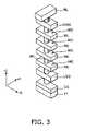
- FIG. 3is a schematic perspective view of one memory string of the memory cell array in FIG. 2 ;
- FIG. 4is a schematic cross-sectional view of the relevant part in the XZ direction in FIG. 2 ;
- FIG. 5is a schematic cross-sectional view of the relevant part in the YZ direction in FIG. 2 ;
- FIGS. 6A to 6Care schematic views illustrating a method for manufacturing the semiconductor memory device according to the embodiment of the invention.
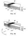
- FIGS. 7A and 7Bare schematic views showing processes continuing from FIGS. 6B ;
- FIGS. 8A and 8Bare schematic views showing processes continuing from FIGS. 7B ;
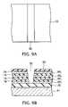
- FIGS. 9A and 9Bare schematic views of the slit formation portion in FIG. 7B ;
- FIGS. 10A and 10Bare schematic views of the state of an interlayer dielectric film buried in the slit shown in FIGS. 9A and 9B ;
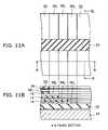
- FIGS. 11A and 11Bare schematic views of a staircase-shaped portion of the stacked body in FIG. 8A ;
- FIG. 12is a B-B cross sectional view in FIG. 11A ;
- FIG. 13is a schematic view showing the pattern layout of the slit dividing the memory cell array of the embodiment of the invention into a plurality of blocks;
- FIG. 14is a schematic view similar to FIG. 14 in a comparative example.
- FIG. 15is a schematic cross-sectional view of the relevant part of the semiconductor memory device according to the embodiment of the invention.
- FIG. 1is a schematic view illustrating the planar layout of major components in a semiconductor memory device according to the embodiment of the invention.
- FIG. 1shows one chip region, which is broadly divided into a memory cell array region and a peripheral circuit region.
- the memory cell array regionis formed at the center of the chip and includes memory cells 3 .
- the peripheral circuit regionis formed around the memory cell array region and includes a sense amplifier 4 , row decoder 5 , and other circuits.
- a stacked body with a plurality of conductive layers and a plurality of dielectric layers alternately stacked, described later,is provided throughout the chip including the memory cell array region and the peripheral circuit region.
- the stacked bodyis divided by slits 30 into a plurality of blocks.
- An interlayer dielectric filmis buried in the slit 30 as described later.
- the component having an independent functionsuch as the memory cell array 3 , sense amplifier 4 , and row decoder 5 , is surrounded by slits 30 formed in a closed (closed-loop) pattern. Furthermore, the memory cell array 3 is divided by slits 30 into a plurality of blocks, each of which is also surrounded by slits 30 formed in a closed (closed-loop) pattern.
- the memory cell array 3is composed of a plurality of memory strings arranged in a two-dimensional array.
- One memory stringis composed of a plurality of memory cells series-connected in the stacking direction of the aforementioned stacked body.
- FIG. 2is a schematic perspective view illustrating the configuration of the memory cell array.
- FIG. 3is a schematic perspective view of one memory string.
- FIG. 4is a schematic cross-sectional view of the relevant part in the XZ direction in FIG. 2 .
- FIG. 5is a schematic cross-sectional view of the relevant part in the YZ direction in FIG. 2 .
- FIGS. 2 and 3for clarity of illustration, only the conductive portions are shown, and the dielectric portions are not shown.
- the semiconductor memory devicehas a structure in which semiconductor layers, dielectric layers, conductive layers, interconnects and the like are formed on a semiconductor substrate.
- the semiconductoris illustratively silicon in this embodiment, other semiconductors can also be used.
- a cell source CSis provided on the silicon substrate 11 .
- the cell source CSis illustratively a silicon layer whose resistance is decreased by impurity doping at relatively high concentration.
- a dielectric layer 12On the cell source CS is provided a dielectric layer 12 , a lower select gate LSG is provided thereon, and a dielectric layer 13 is provided thereon.
- the dielectric layers 12 , 13are illustratively silicon oxide layers, and the lower select gate LSG is illustratively a silicon layer.
- the dielectric layer 12 , the lower select gate LSG, and the dielectric layer 13constitute a stacked body ML 1 .
- the dielectric layer 13is not necessarily needed.
- a stacked body ML 2in which a plurality of dielectric layers 14 illustratively made of silicon oxide and a plurality of conductive layers WL illustratively made of amorphous or polycrystalline silicon are alternately stacked.
- the conductive layer WL in the memory cell arrayfunctions as a word line electrode layer.
- the dielectric layer 14is provided above, below, and between the conductive layers WL, and functions as an interlayer dielectric layer for insulating between the conductive layers WL.
- the number of conductive layers WLis arbitrary, and illustratively four in this embodiment.
- a dielectric layer 15On the stacked body ML 2 is provided a dielectric layer 15 , an upper select gate USG is provided thereon, and a dielectric layer 16 is provided thereon.
- the dielectric layers 15 , 16are illustratively silicon oxide layers, and the upper select gate USG is illustratively a silicon layer.
- the dielectric layer 15 , the upper select gate USG, and the dielectric layer 16constitute a stacked body ML 3 .
- the dielectric layer 16is not necessarily needed.
- an XYZ orthogonal coordinate systemis introduced for convenience of description.
- the two directions parallel to the upper surface (major surface) of the silicon substrate 11 and orthogonal to each otherare referred to as the X and Y direction
- the direction orthogonal to both the X and Y direction, that is, the stacking direction of the dielectric layers 14 and the conductive layers WLis referred to as the Z direction.
- the stacked body ML 1 , the stacked body ML 2 , and the stacked body ML 3(hereinafter also collectively referred to as “stacked body ML”) are divided by the aforementioned slits 30 into a plurality of blocks along the Y direction.
- the upper select gate USGis formed by dividing one plate-like conductive layer (such as a silicon layer) along the Y direction into a plurality of wiring-like conductive members extending in the X direction.
- the conductive layer WL and the lower select gate LSGare formed like a plate parallel to the XY plane.
- the lower select gate LSGcan be divided into a plurality of members like the upper select gate USG.
- the cell source CSis a single plate-like conductive layer parallel to the XY plane so as to connect the immediately underlying regions of the plurality of blocks of the stacked body ML.
- the stacked body MLincludes a plurality of through holes extending in the stacking direction (Z direction) entirely through the stacked body ML.
- the plurality of through holesare arranged in a matrix along the X and Y direction, for instance.
- a silicon pillar SPis buried as a pillar-shaped semiconductor layer.
- the silicon pillar SPis formed from polycrystalline silicon or amorphous silicon.
- the silicon pillar SPis shaped like a pillar, such as a cylinder, extending in the Z direction.
- the silicon pillar SPis provided throughout the stacked body ML in the stacking direction, and its lower end portion is connected to the cell source CS.
- a dielectric layer 18(see FIGS. 4 and 5 ) is provided on the stacked body ML 3 , and a plurality of bit lines BL extending in the Y direction are provided on the dielectric layer 18 .
- the bit line BLis illustratively formed from a metal material. “Metal” referred to herein also includes alloys as well as pure metals.
- Each bit line BLis arranged so as to pass immediately above a corresponding sequence of silicon pillars SP arranged along the Y direction, and is connected to the upper end portion of the silicon pillar SP through a via hole 18 a formed in the dielectric layer 18 . That is, the silicon pillars SP in each sequence arranged in the Y direction are connected to a different bit line BL. Each silicon pillar SP is connected between the bit line BL and the cell source CS.
- the upper select gate USGis connected through a via 20 to an upper select gate interconnect USL illustratively formed from a metal material.
- a plurality of word lines WLL, one lower select gate interconnect LSL, and one cell source interconnect CSLare provided.
- the word line WLL, the lower select gate interconnect LSL, and the cell source interconnect CSLare illustratively formed from a metal material.
- the number of word lines WLL associated with one stacked body blockis equal to the number of conductive layers WL.
- Each word line WLLis connected through a via 21 to the end portion of a corresponding one of the staircase-shaped conductive layers WL.
- the lower select gate interconnect LSLis connected through a via 22 to the lower select gate LSG, and the cell source interconnect CSL is connected through a contact 23 to the cell source CS.
- the interconnectsare insulated from each other by an interlayer dielectric film, not shown.
- a charge storage layer 26is sandwiched between a first dielectric film and a second dielectric film (only the charge storage layer 26 is shown in FIGS. 4 and 5 ). These films are formed in a tubular shape on the inner peripheral wall of the hole.
- the silicon pillar SPis buried inside the second dielectric film, and the second dielectric film is in contact with the silicon pillar SR
- the first dielectric filmis provided in contact with the conductive layers WL, and the charge storage layer 26 is provided between the first dielectric film and the second dielectric film.
- the silicon pillar SP provided in the stacked body ML 2functions as a channel
- the conductive layer WLfunctions as a control gate
- the charge storage layer 26functions as a data memory layer for storing charges injected from the silicon pillar SR That is, at the intersection between the silicon pillar SP and each conductive layer WL is formed a memory cell having a structure in which a channel is surrounded by a gate electrode.
- the memory cellhas a charge trap structure.
- the charge storage layer 26includes numerous traps operable to confine charges (electrons), and is illustratively made of a silicon nitride film.
- the second dielectric filmis illustratively made of a silicon oxide film and serves as a potential barrier when a charge is injected from the silicon pillar SP into the charge storage layer 26 or when a charge stored in the charge storage layer 26 diffuses into the silicon pillar SP.
- the first dielectric filmis illustratively made of a silicon oxide film and prevents charges stored in the charge storage layer 26 from diffusing into the conductive layer WL which functions as a gate electrode.
- the memory cellincludes no diffusion layer serving as a source/drain region having a different conductivity type in the silicon pillar SR That is, the silicon pillar SP functions as a channel region, source region, and drain region in the memory cell. Furthermore, the OFF state is realized by controlling the voltage applied to the conductive layer WL to substantially deplete the silicon pillar SP opposed to the conductive layer WL.
- memory stringsare arranged in a matrix in the X and Y direction, and thereby a plurality of memory cells are three-dimensionally arranged in the X, Y, and Z direction.
- the stacked body ML 1includes a lower select transistor LST with the silicon pillar SP serving as a channel and the lower select gate LSG therearound serving as a gate electrode.
- the stacked body ML 3includes an upper select transistor UST with the silicon pillar SP serving as a channel and the upper select gate USG therearound serving as a gate electrode.
- the lower select transistor LST and the upper select transistor USThave a structure in which a channel is surrounded by a gate electrode, like the aforementioned memory cell. However, they do not function as memory cells, but serves to select a silicon pillar SP.
- the semiconductor memory deviceincludes a driver circuit for applying a potential to the upper end portion of the silicon pillar SP through the bit line BL, a driver circuit for applying a potential to the lower end portion of the silicon pillar SP through the cell source interconnect CSL, the contact 23 , and the cell source CS, a driver circuit for applying a potential to the upper select gate USG through the upper select gate interconnect USL and the via 20 , a driver circuit for applying a potential to the lower select gate LSG through the lower select gate interconnect LSL and the via 22 , and a driver circuit (corresponding to the row decoder 5 shown in FIG. 1 ) for applying a potential to each conductive layer WL through the word line WLL and the via 21 .
- These driver circuitsare formed in the peripheral circuit region shown in FIG. 1 .
- the peripheral circuit regionincludes P-wells and N-wells (not shown), in which transistors and other elements are formed.
- the semiconductor memory deviceis a nonvolatile semiconductor memory device allowing data to be erased and written electrically and freely, and being capable of retaining its memory content even when powered off.
- the X coordinate of a memory cellis selected by selecting a bit line BL
- the Y coordinate of the memory cellis selected by selecting an upper select gate USG to turn the upper select transistor UST to the conducting or non-conducting state
- the Z coordinate of the memory cellis selected by using the row decoder 5 to select a conductive layer WL serving as a word line. Then, information is stored by injecting electrons into the charge storage layer 26 of the selected memory cell.
- the data stored in the memory cellis read by passing a sense current in the silicon pillar SP which passes through the memory cell.
- FIGS. 6 to 8show a method for manufacturing the memory cell array. In FIGS. 6 to 8 , only the conductive portions are shown, and the dielectric portions are not shown.
- an element isolation trench having an STI (shallow trench isolation) structureis formed.
- a dielectric filmis buried in the element isolation trench.
- a silicon layer constituting a lower select gate LSGis formed via a dielectric layer above the cell source CS, and a dielectric layer is formed further thereon.
- the stacked body ML 1 shown in FIGS. 4 and 5is obtained.
- P-wells, N-wells and the likeare formed in the peripheral circuit region, the gates of transistors constituting driver circuits (such as a sense amplifier 4 and row decoder 5 ) are formed, and their sources/drains are formed.
- a dielectric filmsuch as a silicon oxide film and a silicon nitride film, is deposited entirely on the stacked body ML 1 .
- the dielectric filmis formed on the bottom surface and side surface of the through hole in addition to the upper surface of the stacked body ML 1 .
- the dielectric film formed on the upper surface of the stacked body ML 1 and the bottom surface of the through holeis removed illustratively by RIE (reactive ion etching).
- RIEreactive ion etching
- the dielectric filmremains on the side surface of the through hole to serve as a gate dielectric film GD ( FIGS. 4 and 5 ).
- siliconis buried inside the through hole to form a silicon pillar SP in the through hole.
- a lower select transistor LSTis formed.
- dielectric films 14illustratively made of TEOS (tetraethoxysilane) and conductive layers WL illustratively made of amorphous or polycrystalline silicon are alternately stacked to form a stacked body ML 2 .
- TEOStetraethoxysilane
- conductive layers WLillustratively made of amorphous or polycrystalline silicon
- holes penetrating through the stacked body ML 2 of the dielectric films 14 and the conductive layers WL and extending in the stacking direction thereofare formed by RIE (reactive ion etching).
- the holeis formed immediately above the silicon pillar SP of the underlying stacked body ML 1 so as to reach that silicon pillar SP.
- a dielectric film illustratively having an ONO (oxide-nitride-oxide) structure including a charge storage layer 26(this dielectric film being hereinafter simply referred to as ONO film) is formed.
- ONO filmis formed on the bottom surface and side surface of the hole in addition to the upper surface of the stacked body ML 2 .
- the ONO film formed on the upper surface of the stacked body ML 2 and the bottom surface of the holeis removed.
- the ONO filmis left only on the side surface of the hole.
- siliconis buried inside the hole to form a silicon pillar SP in the stacked body ML 2 ( FIG. 7A ).
- a memory cellis formed at the intersection between the silicon pillar SP and each conductive layer WL.
- the lower end of the silicon pillar SP of the stacked body ML 2is in contact with the upper end of the silicon pillar SP of the stacked body ML 1 .
- a slit 30is formed to divide the stacked body ML 2 .
- This slit 30is formed illustratively by RIE (reactive ion etching).
- This slit 30divides the memory cell array into a plurality of blocks in the Y direction. Erasure of data, for instance, is collectively performed for each block.
- FIG. 9Ais an enlarged schematic plan view of the slit formation portion, and FIG. 9B is a cross-sectional view of that portion.
- a silicon nitride film 33is formed in advance on top of the stacked body ML 2 .
- the lower select transistor LST shown in FIGS. 4 and 5is not shown, and the dielectric layer on the lower select transistor LST is shown as a dielectric layer 32 .
- FIGS. 10A and 10Bshow the states after burying of the interlayer dielectric film 31 , corresponding to FIGS. 9A and 9B , respectively.
- a silicon oxide filmis deposited on the stacked body including inside the slit 30 , and then planarized by CMP (chemical mechanical polishing) using the silicon nitride film 33 on top of the stacked body as a stopper.
- CMPchemical mechanical polishing
- a photoresist film(not shown) is formed on the stacked body ML 2 (on the silicon nitride film 32 ) and patterned into a rectangular shape, for instance. Then, the process of patterning the dielectric films 14 and the conductive films WL by RIE using the photoresist film as a mask, the process of ashing (slimming) the photoresist film to downsize its outline, the process of patterning the dielectric films 14 and the conductive films WL by using the slimmed photoresist film as a mask, the process of further slimming the photoresist film, and so on, are repeated to pattern the end portion of the stacked body of the dielectric films 14 and the conductive films WL into a staircase shape as shown in FIGS. 8A and 11 .
- FIG. 11Ais a schematic plan view of the aforementioned staircase-shaped portion
- FIG. 11Bis an A-A cross-sectional view in FIG. 11A
- FIG. 12is a B-B cross-sectional view in FIG. 11A .
- the portion including the slit 30 dividing the stacked body into a plurality of blocks and the interlayer dielectric film 31 buried thereinis not etched but left as shown in FIG. 12 .
- the slit 30is illustratively formed by RIE. Under the current process technology, particularly in the case where the stacked body includes a large number of layers and has a large aspect ratio, the width of the slit 30 is not constant along the depth, but tends to narrow from the upper portion on the opening end side toward the lower (bottom) portion as shown in FIG. 9B .
- the interlayer dielectric film 31 on the opening end side, where the slit 30 is wideacts as a mask and prevents the conductive layers WL located therebelow from being etched.
- a portion WLa of the conductive layer WLremains beside (outside) the sidewall of the slit 30 .
- FIG. 14shows a pattern layout of a slit 30 in a comparative example corresponding to this embodiment.
- the region where the residual conductive layer WLa exists beside the sidewall of the slit 30is schematically shown by dashed hatching.
- the slit 30extends only in the direction crossing (orthogonal to) each end portion of the staircase-shaped conductive layers WL, and the stacked body including the conductive layers WL is divided into blocks BL 1 -BL 3 .
- the residual conductive layer WLa of the block BL 1 and the residual conductive layer WLa of the block BL 2are connected through a portion formed so as to circumvent the end portion of the slit 30 .
- the residual conductive layer WLa of the block BL 2 and the residual conductive layer WLa of the block BL 3are connected through a portion formed so as to circumvent the end portion of the slit 30 . That is, in the comparative example shown in FIG. 14 , the conductive layers WL of the adjacent blocks across the slit 30 are short-circuited to each other through the residual conductive layer WLa.
- FIGS. 1 and 13the pattern layout of the slit 30 in this embodiment is shown in FIGS. 1 and 13 . Also in FIG. 13 , like FIG. 14 , the region where the residual conductive layer WLa exists beside the sidewall of the slit 30 is schematically shown by dashed hatching.
- the slit 30also extends in the direction along the block dividing direction, and each block is surrounded by the slits 30 formed in a closed (closed-loop) pattern.
- the residual conductive layer WLa of each blockalso has a closed-loop pattern which is closed in the block, and avoids connection between the residual conductive layers WLa of the adjacent blocks. Consequently, short circuit of the conductive layers WL between the blocks can be avoided.
- a barrier layer(such as a silicon nitride film) 35 is deposited on the staircase-shaped portion.
- an interlayer dielectric film(such as a silicon oxide film) 36 is buried further thereon and planarized by CMP.
- the conductive layers WL and the lower select gate LSGare each electrically extracted above through contact portions 65 , 64 .
- An upper select gate USGis formed via a dielectric layer above the stacked body ML 2 in the memory cell array ( FIG. 8B ), and a dielectric layer is formed further thereon.
- the stacked body ML 3 shown in FIGS. 4 and 5is formed.
- a dielectric filmsuch as a silicon oxide film and a silicon nitride film, is deposited entirely on the stacked body ML 3 .
- This dielectric filmis formed on the bottom surface and side surface of the through hole in addition to the upper surface of the stacked body ML 3 .
- the dielectric film formed on the upper surface of the stacked body ML 3 and the bottom surface of the through holeis removed illustratively by RIE.
- the dielectric filmremains on the side surface of the through hole to serve as a gate dielectric film GD ( FIGS. 4 and 5 ).
- silicon pillar SP of the stacked body ML 2is exposed to the bottom of the through hole, silicon is buried inside the through hole to form a silicon pillar SP in the stacked body ML 3 .
- an upper select transistor USTis formed.
- the lower end of the silicon pillar SP of the stacked body ML 3is in contact with the upper end of the silicon pillar SP of the underlying stacked body ML 2 .
- the upper select gate USGis electrically extracted above through a contact portion 61 .
- bit lines BLbit lines BL, upper select gate interconnects USL, word lines WLL, lower select gate interconnects LSL, cell source interconnects CSL and the like are formed.
- bit lines BLbit lines BL, upper select gate interconnects USL, word lines WLL, lower select gate interconnects LSL, cell source interconnects CSL and the like are formed.
- FIG. 15The cross-sectional view of FIG. 15 described above also shows part of the peripheral circuit region 200 .
- thin hatchingrepresents a conductive layer
- thick hatchingrepresents a dielectric layer.
- the peripheral circuit region 200also includes a stacked body in which a plurality of conductive layers WL and a plurality of dielectric layers 14 are alternately stacked.
- the stacked body of the conductive layers WL and the dielectric layers 14is formed entirely on the substrate 11 , and the stacked body in the peripheral circuit region 200 is left therein without removal.
- the stacked body in the peripheral circuit region 200is a so-called dummy structure for avoiding a large step difference with respect to the memory cell array region 100 , and the conductive layer WL in the peripheral circuit region 200 does not function as an electrode or interconnect layer.
- the conductive layer 57 in the peripheral circuit region 200is formed in the same process as the conductive layer constituting the lower select gate LSG in the memory cell array region 100 , and functions as the gate electrode of a transistor formed in the peripheral circuit region 200 .
- This gate electrode 57is electrically extracted above through a contact portion 63 penetrating through the dielectric layers 36 , 37 , the barrier layer 35 and the like.
- the aforementioned stacked bodyis provided also in the peripheral circuit region 200 .
- the stacked body of the conductive layers WL and the dielectric layers 14is provided also in and around the region including the sense amplifier 4 and the row decoder 5 shown in FIG. 1 .
- the stacked body around the sense amplifier 4is also provided with slits 30 in a closed (closed-loop) pattern surrounding the sense amplifier 4 .
- the stacked body around the row decoder 5is also provided with slits 30 in a closed (closed-loop) pattern surrounding the row decoder 5 .
- the residual conductive layers in each region of the sense amplifier 4 and the row decoder 5form a closed-loop pattern.
- the residual conductive layersare not connected to those of the memory cell array 3 and other peripheral circuit components.
- the embodiment of the inventioncan avoid short circuit between components through residual conductive layers which may remain beside the sidewall of the slit 30 for insulating and isolating between the components intended to be electrically independent.
- slits 30 with an interlayer dielectric film buried thereinare formed also immediately inside the dicing line for chip separation and entirely surround the chip in a closed-loop pattern. Even if a crack occurs at the chip edge during dicing, the slit 30 with an interlayer dielectric film buried therein functions as a buffer layer and can prevent the crack from reaching the peripheral circuit or memory cell array located inside.
- the portion inside the dicing linecan also be patterned into a staircase shape like the end portion of the memory cell array. This also serves to prevent cracks from reaching the inner components.
- the shape of the silicon pillar SPis not limited to a cylinder, but can be a prism. Furthermore, the invention is not limited to burying a silicon pillar entirely in the through hole. As an alternative structure, a silicon pillar can be formed in a tubular shape only at the portion in contact with the ONO film, and a dielectric can be buried inside it. Furthermore, the film structure between the conductive layer WL and the silicon pillar is not limited to the ONO film structure, but can be a two-layer structure of a charge storage layer and a gate dielectric film, for instance.
Landscapes
- Semiconductor Memories (AREA)
- Non-Volatile Memory (AREA)
Abstract
Description
- This application is based upon and claims the benefit of priority from the prior Japanese Patent Application No. 2008-282817, filed on Nov. 4, 2008; the entire contents of which are incorporated herein by reference.
- 1. Field of the Invention
- This invention relates to a semiconductor memory device having a three-dimensional memory cell array structure in which electrode layers are stacked to form memory cells densely arranged in the electrode stacking direction.
- 2. Background Art
- Conventional stacked memory technology is based on the structure of layers stacked by repeating for each layer the process of forming normal, planar memory cells on a silicon substrate. This structure is unsuitable for large capacity because it requires many manufacturing steps per layer. In this context, a technique for increasing the capacity with high manufacturing efficiency is proposed (e.g., JP-A-2007-266143(Kokai)). In this technique, gate electrode layers and interlayer dielectric layers are alternately stacked into a stacked structure. Holes penetrating therethrough from the uppermost layer to the lowermost layer are formed at once, and silicon is buried therein in a pillar shape. In the resulting structure, the silicon pillar is covered with the gate electrode layers at certain intervals. A memory cell transistor is formed by providing a charge storage layer for data retention at the intersection between the gate electrode layer and the silicon pillar.
- In such a collectively patterned stacked memory, to separate the memory cell array into a plurality of blocks, the stacked body including the word line electrode layers is divided by slits with an interlayer dielectric film buried therein. Furthermore, for electrical contact to each word line electrode layer, the end portion of the word line electrode layers is patterned into a staircase shape. In this staircase patterning, that is, in etching away the unwanted portion of the word line electrode layers, the word line electrode layer may partly remain beside the slit sidewall under the current process technology. Depending on the slit pattern layout, there is concern about the problem of short circuit between the word line electrode layers of adjacent blocks or regions across the slit through the residual electrode layers beside the slit.
- According to an aspect of the invention, there is provided a semiconductor memory device including: a semiconductor substrate; a stacked body with a plurality of conductive layers and a plurality of dielectric layers alternately stacked, the stacked body being provided on the semiconductor substrate; a semiconductor layer provided inside a hole formed through the stacked body, the semiconductor layer extending in stacking direction of the conductive layers and the dielectric layers; and a charge storage layer provided between the conductive layers and the semiconductor layer, the stacked body in a memory cell array region including a plurality of memory strings being divided into a plurality of blocks by slits with an interlayer dielectric film buried therein, the memory string including as many memory cells series-connected in the stacking direction as the conductive layers, the memory cell including the conductive layer, the semiconductor layer, and the charge storage layer provided between the conductive layer and the semiconductor layer, and each of the block being surrounded by the slits formed in a closed pattern.
FIG. 1 is a schematic view illustrating the planar layout of major components in a semiconductor memory device according to an embodiment of the invention;FIG. 2 is a schematic perspective view illustrating the configuration of a memory cell array of the semiconductor memory device;FIG. 3 is a schematic perspective view of one memory string of the memory cell array inFIG. 2 ;FIG. 4 is a schematic cross-sectional view of the relevant part in the XZ direction inFIG. 2 ;FIG. 5 is a schematic cross-sectional view of the relevant part in the YZ direction inFIG. 2 ;FIGS. 6A to 6C are schematic views illustrating a method for manufacturing the semiconductor memory device according to the embodiment of the invention;FIGS. 7A and 7B are schematic views showing processes continuing fromFIGS. 6B ;FIGS. 8A and 8B are schematic views showing processes continuing fromFIGS. 7B ;FIGS. 9A and 9B are schematic views of the slit formation portion inFIG. 7B ;FIGS. 10A and 10B are schematic views of the state of an interlayer dielectric film buried in the slit shown inFIGS. 9A and 9B ;FIGS. 11A and 11B are schematic views of a staircase-shaped portion of the stacked body inFIG. 8A ;FIG. 12 is a B-B cross sectional view inFIG. 11A ;FIG. 13 is a schematic view showing the pattern layout of the slit dividing the memory cell array of the embodiment of the invention into a plurality of blocks;FIG. 14 is a schematic view similar toFIG. 14 in a comparative example; andFIG. 15 is a schematic cross-sectional view of the relevant part of the semiconductor memory device according to the embodiment of the invention.- An embodiment of the invention will now be described with reference to the drawings.
FIG. 1 is a schematic view illustrating the planar layout of major components in a semiconductor memory device according to the embodiment of the invention.FIG. 1 shows one chip region, which is broadly divided into a memory cell array region and a peripheral circuit region. The memory cell array region is formed at the center of the chip and includesmemory cells 3. The peripheral circuit region is formed around the memory cell array region and includes asense amplifier 4,row decoder 5, and other circuits.- A stacked body with a plurality of conductive layers and a plurality of dielectric layers alternately stacked, described later, is provided throughout the chip including the memory cell array region and the peripheral circuit region. The stacked body is divided by
slits 30 into a plurality of blocks. An interlayer dielectric film is buried in theslit 30 as described later. - The component having an independent function, such as the
memory cell array 3,sense amplifier 4, androw decoder 5, is surrounded byslits 30 formed in a closed (closed-loop) pattern. Furthermore, thememory cell array 3 is divided byslits 30 into a plurality of blocks, each of which is also surrounded byslits 30 formed in a closed (closed-loop) pattern. - The
memory cell array 3 is composed of a plurality of memory strings arranged in a two-dimensional array. One memory string is composed of a plurality of memory cells series-connected in the stacking direction of the aforementioned stacked body. - In the following, the configuration of the memory cell array in the semiconductor memory device according to this embodiment is described with reference to
FIGS. 2 to 5 . FIG. 2 is a schematic perspective view illustrating the configuration of the memory cell array.FIG. 3 is a schematic perspective view of one memory string.FIG. 4 is a schematic cross-sectional view of the relevant part in the XZ direction inFIG. 2 .FIG. 5 is a schematic cross-sectional view of the relevant part in the YZ direction inFIG. 2 .- In
FIGS. 2 and 3 , for clarity of illustration, only the conductive portions are shown, and the dielectric portions are not shown. - The semiconductor memory device according to this embodiment has a structure in which semiconductor layers, dielectric layers, conductive layers, interconnects and the like are formed on a semiconductor substrate. Although the semiconductor is illustratively silicon in this embodiment, other semiconductors can also be used.
- As shown in
FIGS. 4 and 5 , a cell source CS is provided on thesilicon substrate 11. The cell source CS is illustratively a silicon layer whose resistance is decreased by impurity doping at relatively high concentration. On the cell source CS is provided adielectric layer 12, a lower select gate LSG is provided thereon, and adielectric layer 13 is provided thereon. The dielectric layers12,13 are illustratively silicon oxide layers, and the lower select gate LSG is illustratively a silicon layer. Thedielectric layer 12, the lower select gate LSG, and thedielectric layer 13 constitute a stacked body ML1. Here, thedielectric layer 13 is not necessarily needed. - On the stacked body ML1 is provided a stacked body ML2 in which a plurality of
dielectric layers 14 illustratively made of silicon oxide and a plurality of conductive layers WL illustratively made of amorphous or polycrystalline silicon are alternately stacked. - The conductive layer WL in the memory cell array functions as a word line electrode layer. The
dielectric layer 14 is provided above, below, and between the conductive layers WL, and functions as an interlayer dielectric layer for insulating between the conductive layers WL. The number of conductive layers WL is arbitrary, and illustratively four in this embodiment. - On the stacked body ML2 is provided a
dielectric layer 15, an upper select gate USG is provided thereon, and adielectric layer 16 is provided thereon. The dielectric layers15,16 are illustratively silicon oxide layers, and the upper select gate USG is illustratively a silicon layer. Thedielectric layer 15, the upper select gate USG, and thedielectric layer 16 constitute a stacked body ML3. Here, thedielectric layer 16 is not necessarily needed. - In the following, in this specification, an XYZ orthogonal coordinate system is introduced for convenience of description. In this coordinate system, the two directions parallel to the upper surface (major surface) of the
silicon substrate 11 and orthogonal to each other are referred to as the X and Y direction, and the direction orthogonal to both the X and Y direction, that is, the stacking direction of thedielectric layers 14 and the conductive layers WL, is referred to as the Z direction. The stacked body ML1, the stacked body ML2, and the stacked body ML3 (hereinafter also collectively referred to as “stacked body ML”) are divided by theaforementioned slits 30 into a plurality of blocks along the Y direction. - The upper select gate USG is formed by dividing one plate-like conductive layer (such as a silicon layer) along the Y direction into a plurality of wiring-like conductive members extending in the X direction.
- The conductive layer WL and the lower select gate LSG are formed like a plate parallel to the XY plane. Alternatively, the lower select gate LSG can be divided into a plurality of members like the upper select gate USG. The cell source CS is a single plate-like conductive layer parallel to the XY plane so as to connect the immediately underlying regions of the plurality of blocks of the stacked body ML.
- The stacked body ML includes a plurality of through holes extending in the stacking direction (Z direction) entirely through the stacked body ML. The plurality of through holes are arranged in a matrix along the X and Y direction, for instance.
- Inside each through hole, a silicon pillar SP is buried as a pillar-shaped semiconductor layer. The silicon pillar SP is formed from polycrystalline silicon or amorphous silicon. The silicon pillar SP is shaped like a pillar, such as a cylinder, extending in the Z direction. The silicon pillar SP is provided throughout the stacked body ML in the stacking direction, and its lower end portion is connected to the cell source CS.
- A dielectric layer18 (see
FIGS. 4 and 5 ) is provided on the stacked body ML3, and a plurality of bit lines BL extending in the Y direction are provided on thedielectric layer 18. The bit line BL is illustratively formed from a metal material. “Metal” referred to herein also includes alloys as well as pure metals. - Each bit line BL is arranged so as to pass immediately above a corresponding sequence of silicon pillars SP arranged along the Y direction, and is connected to the upper end portion of the silicon pillar SP through a via
hole 18aformed in thedielectric layer 18. That is, the silicon pillars SP in each sequence arranged in the Y direction are connected to a different bit line BL. Each silicon pillar SP is connected between the bit line BL and the cell source CS. - As shown in
FIG. 2 , the upper select gate USG is connected through a via20 to an upper select gate interconnect USL illustratively formed from a metal material. - For each block of the stacked body ML, a plurality of word lines WLL, one lower select gate interconnect LSL, and one cell source interconnect CSL are provided. The word line WLL, the lower select gate interconnect LSL, and the cell source interconnect CSL are illustratively formed from a metal material.
- The number of word lines WLL associated with one stacked body block is equal to the number of conductive layers WL. Each word line WLL is connected through a via21 to the end portion of a corresponding one of the staircase-shaped conductive layers WL. The lower select gate interconnect LSL is connected through a via22 to the lower select gate LSG, and the cell source interconnect CSL is connected through a
contact 23 to the cell source CS. The interconnects are insulated from each other by an interlayer dielectric film, not shown. - On the inner peripheral wall of the hole formed in the stacked body ML2 made of the stacked structure of the conductive layers WL and the
dielectric layers 14 is formed a structure in which acharge storage layer 26 is sandwiched between a first dielectric film and a second dielectric film (only thecharge storage layer 26 is shown inFIGS. 4 and 5 ). These films are formed in a tubular shape on the inner peripheral wall of the hole. - The silicon pillar SP is buried inside the second dielectric film, and the second dielectric film is in contact with the silicon pillar SR The first dielectric film is provided in contact with the conductive layers WL, and the
charge storage layer 26 is provided between the first dielectric film and the second dielectric film. - The silicon pillar SP provided in the stacked body ML2 functions as a channel, the conductive layer WL functions as a control gate, and the
charge storage layer 26 functions as a data memory layer for storing charges injected from the silicon pillar SR That is, at the intersection between the silicon pillar SP and each conductive layer WL is formed a memory cell having a structure in which a channel is surrounded by a gate electrode. - The memory cell has a charge trap structure. The
charge storage layer 26 includes numerous traps operable to confine charges (electrons), and is illustratively made of a silicon nitride film. The second dielectric film is illustratively made of a silicon oxide film and serves as a potential barrier when a charge is injected from the silicon pillar SP into thecharge storage layer 26 or when a charge stored in thecharge storage layer 26 diffuses into the silicon pillar SP. The first dielectric film is illustratively made of a silicon oxide film and prevents charges stored in thecharge storage layer 26 from diffusing into the conductive layer WL which functions as a gate electrode. - Downscaling of the memory cell having the aforementioned structure allows normal write/read operation to be performed without diffusion layers serving as source/drain regions. Hence, in this embodiment, the memory cell includes no diffusion layer serving as a source/drain region having a different conductivity type in the silicon pillar SR That is, the silicon pillar SP functions as a channel region, source region, and drain region in the memory cell. Furthermore, the OFF state is realized by controlling the voltage applied to the conductive layer WL to substantially deplete the silicon pillar SP opposed to the conductive layer WL.
- As shown in
FIG. 3 , as many memory cells MC as the conductive layers WL are series connected in the Z direction around one silicon pillar SP to constitute one memory string. Such memory strings are arranged in a matrix in the X and Y direction, and thereby a plurality of memory cells are three-dimensionally arranged in the X, Y, and Z direction. - Referring again to
FIGS. 4 and 5 , on the inner peripheral wall of the through hole formed in the stacked body ML1 below the stacked body ML2, a gate dielectric film GD is formed in a tubular shape, and the silicon pillar SP is buried therein. Thus, the stacked body ML1 includes a lower select transistor LST with the silicon pillar SP serving as a channel and the lower select gate LSG therearound serving as a gate electrode. - Furthermore, on the inner peripheral wall of the through hole formed in the stacked body ML3 above the stacked body ML2, a gate dielectric film GD is formed in a tubular shape, and the silicon pillar SP is buried therein. Thus, the stacked body ML3 includes an upper select transistor UST with the silicon pillar SP serving as a channel and the upper select gate USG therearound serving as a gate electrode.
- The lower select transistor LST and the upper select transistor UST have a structure in which a channel is surrounded by a gate electrode, like the aforementioned memory cell. However, they do not function as memory cells, but serves to select a silicon pillar SP.
- Furthermore, the semiconductor memory device according to this embodiment includes a driver circuit for applying a potential to the upper end portion of the silicon pillar SP through the bit line BL, a driver circuit for applying a potential to the lower end portion of the silicon pillar SP through the cell source interconnect CSL, the
contact 23, and the cell source CS, a driver circuit for applying a potential to the upper select gate USG through the upper select gate interconnect USL and the via20, a driver circuit for applying a potential to the lower select gate LSG through the lower select gate interconnect LSL and the via22, and a driver circuit (corresponding to therow decoder 5 shown inFIG. 1 ) for applying a potential to each conductive layer WL through the word line WLL and the via21. These driver circuits are formed in the peripheral circuit region shown inFIG. 1 . The peripheral circuit region includes P-wells and N-wells (not shown), in which transistors and other elements are formed. - The semiconductor memory device according to this embodiment is a nonvolatile semiconductor memory device allowing data to be erased and written electrically and freely, and being capable of retaining its memory content even when powered off.
- The X coordinate of a memory cell is selected by selecting a bit line BL, the Y coordinate of the memory cell is selected by selecting an upper select gate USG to turn the upper select transistor UST to the conducting or non-conducting state, and the Z coordinate of the memory cell is selected by using the
row decoder 5 to select a conductive layer WL serving as a word line. Then, information is stored by injecting electrons into thecharge storage layer 26 of the selected memory cell. The data stored in the memory cell is read by passing a sense current in the silicon pillar SP which passes through the memory cell. - Next, a method for manufacturing the semiconductor memory device according to this embodiment is described with reference to
FIGS. 6 to 8 in addition toFIGS. 4 and 5 described above.FIGS. 6 to 8 show a method for manufacturing the memory cell array. InFIGS. 6 to 8 , only the conductive portions are shown, and the dielectric portions are not shown. - After a cell source CS is formed on a silicon substrate11 (
FIGS. 4 and 5 ), as shown inFIG. 6A , an element isolation trench having an STI (shallow trench isolation) structure, for instance, is formed. A dielectric film is buried in the element isolation trench. - Next, as shown in
FIG. 6B , a silicon layer constituting a lower select gate LSG is formed via a dielectric layer above the cell source CS, and a dielectric layer is formed further thereon. Thus, the stacked body ML1 shown inFIGS. 4 and 5 is obtained. Simultaneously, P-wells, N-wells and the like are formed in the peripheral circuit region, the gates of transistors constituting driver circuits (such as asense amplifier 4 and row decoder5) are formed, and their sources/drains are formed. - Next, in the stacked body ML1, through holes extending in the Z direction (stacking direction) to the cell source CS are etched, and then a dielectric film, such as a silicon oxide film and a silicon nitride film, is deposited entirely on the stacked body ML1. The dielectric film is formed on the bottom surface and side surface of the through hole in addition to the upper surface of the stacked body ML1. Then, the dielectric film formed on the upper surface of the stacked body ML1 and the bottom surface of the through hole is removed illustratively by RIE (reactive ion etching). Thus, the dielectric film remains on the side surface of the through hole to serve as a gate dielectric film GD (
FIGS. 4 and 5 ). Next, silicon is buried inside the through hole to form a silicon pillar SP in the through hole. Thus, a lower select transistor LST is formed. - Next, as shown in
FIGS. 4 ,5, and6C, on the stacked body ML1,dielectric films 14 illustratively made of TEOS (tetraethoxysilane) and conductive layers WL illustratively made of amorphous or polycrystalline silicon are alternately stacked to form a stacked body ML2. - Next, holes penetrating through the stacked body ML2 of the
dielectric films 14 and the conductive layers WL and extending in the stacking direction thereof are formed by RIE (reactive ion etching). The hole is formed immediately above the silicon pillar SP of the underlying stacked body ML1 so as to reach that silicon pillar SP. - After the aforementioned holes are formed, a dielectric film illustratively having an ONO (oxide-nitride-oxide) structure including a charge storage layer26 (this dielectric film being hereinafter simply referred to as ONO film) is formed. The ONO film is formed on the bottom surface and side surface of the hole in addition to the upper surface of the stacked body ML2.
- Next, the ONO film formed on the upper surface of the stacked body ML2 and the bottom surface of the hole is removed. Thus, the ONO film is left only on the side surface of the hole.
- Then, silicon is buried inside the hole to form a silicon pillar SP in the stacked body ML2 (
FIG. 7A ). Thus, a memory cell is formed at the intersection between the silicon pillar SP and each conductive layer WL. The lower end of the silicon pillar SP of the stacked body ML2 is in contact with the upper end of the silicon pillar SP of the stacked body ML1. - Next, for the purpose of dividing the memory cell array into a plurality of blocks, as shown in
FIG. 7B , aslit 30 is formed to divide the stacked body ML2. This slit30 is formed illustratively by RIE (reactive ion etching). This slit30 divides the memory cell array into a plurality of blocks in the Y direction. Erasure of data, for instance, is collectively performed for each block. FIG. 9A is an enlarged schematic plan view of the slit formation portion, andFIG. 9B is a cross-sectional view of that portion. Before theslit 30 is formed, asilicon nitride film 33 is formed in advance on top of the stacked body ML2. InFIG. 9B , the lower select transistor LST shown inFIGS. 4 and 5 is not shown, and the dielectric layer on the lower select transistor LST is shown as adielectric layer 32.- After the
slit 30 is formed, aninterlayer dielectric film 31 is buried in theslit 30 as shown inFIG. 10 .FIGS. 10A and 10B show the states after burying of theinterlayer dielectric film 31, corresponding toFIGS. 9A and 9B , respectively. Specifically, a silicon oxide film is deposited on the stacked body including inside theslit 30, and then planarized by CMP (chemical mechanical polishing) using thesilicon nitride film 33 on top of the stacked body as a stopper. Thus, the structure ofFIG. 10B is obtained. - Next, a photoresist film (not shown) is formed on the stacked body ML2 (on the silicon nitride film32) and patterned into a rectangular shape, for instance. Then, the process of patterning the
dielectric films 14 and the conductive films WL by RIE using the photoresist film as a mask, the process of ashing (slimming) the photoresist film to downsize its outline, the process of patterning thedielectric films 14 and the conductive films WL by using the slimmed photoresist film as a mask, the process of further slimming the photoresist film, and so on, are repeated to pattern the end portion of the stacked body of thedielectric films 14 and the conductive films WL into a staircase shape as shown inFIGS. 8A and 11 . FIG. 11A is a schematic plan view of the aforementioned staircase-shaped portion, andFIG. 11B is an A-A cross-sectional view inFIG. 11A .FIG. 12 is a B-B cross-sectional view inFIG. 11A .- In the aforementioned staircase patterning of the stacked body, the portion including the
slit 30 dividing the stacked body into a plurality of blocks and theinterlayer dielectric film 31 buried therein is not etched but left as shown inFIG. 12 . - The
slit 30 is illustratively formed by RIE. Under the current process technology, particularly in the case where the stacked body includes a large number of layers and has a large aspect ratio, the width of theslit 30 is not constant along the depth, but tends to narrow from the upper portion on the opening end side toward the lower (bottom) portion as shown inFIG. 9B . - Hence, if the end portion of the
dielectric films 14 and the conductive films WL is etched into a staircase shape as described above, theinterlayer dielectric film 31 on the opening end side, where theslit 30 is wide, acts as a mask and prevents the conductive layers WL located therebelow from being etched. Thus, as shown inFIG. 12 , a portion WLa of the conductive layer WL remains beside (outside) the sidewall of theslit 30. - Here,
FIG. 14 shows a pattern layout of aslit 30 in a comparative example corresponding to this embodiment. InFIG. 14 , the region where the residual conductive layer WLa exists beside the sidewall of theslit 30 is schematically shown by dashed hatching. - In this comparative example, the
slit 30 extends only in the direction crossing (orthogonal to) each end portion of the staircase-shaped conductive layers WL, and the stacked body including the conductive layers WL is divided into blocks BL1-BL3. In such a pattern layout, the residual conductive layer WLa of the block BL1 and the residual conductive layer WLa of the block BL2 are connected through a portion formed so as to circumvent the end portion of theslit 30. Likewise, the residual conductive layer WLa of the block BL2 and the residual conductive layer WLa of the block BL3 are connected through a portion formed so as to circumvent the end portion of theslit 30. That is, in the comparative example shown inFIG. 14 , the conductive layers WL of the adjacent blocks across theslit 30 are short-circuited to each other through the residual conductive layer WLa. - In contrast, the pattern layout of the
slit 30 in this embodiment is shown inFIGS. 1 and 13 . Also inFIG. 13 , likeFIG. 14 , the region where the residual conductive layer WLa exists beside the sidewall of theslit 30 is schematically shown by dashed hatching. - In this embodiment, the
slit 30 also extends in the direction along the block dividing direction, and each block is surrounded by theslits 30 formed in a closed (closed-loop) pattern. Hence, the residual conductive layer WLa of each block also has a closed-loop pattern which is closed in the block, and avoids connection between the residual conductive layers WLa of the adjacent blocks. Consequently, short circuit of the conductive layers WL between the blocks can be avoided. - After the end portion of the conductive layers WL in the memory cell array is patterned into a staircase shape as described above, as shown in
FIG. 15 , a barrier layer (such as a silicon nitride film)35 is deposited on the staircase-shaped portion. Then, an interlayer dielectric film (such as a silicon oxide film)36 is buried further thereon and planarized by CMP. - Contact holes reaching the end portion of the staircase-shaped conductive layers WL and the lower select gate
- LSG are formed through the
barrier layer 35 and theinterlayer dielectric film 36, and a conductive material is buried therein. Thus, the conductive layers WL and the lower select gate LSG are each electrically extracted above throughcontact portions - The process is further continued. An upper select gate USG is formed via a dielectric layer above the stacked body ML2 in the memory cell array (
FIG. 8B ), and a dielectric layer is formed further thereon. Thus, the stacked body ML3 shown inFIGS. 4 and 5 is formed. - In the stacked body ML3, through holes extending in the Z direction (stacking direction) to the silicon pillar SP of the stacked body ML2 are etched, and then a dielectric film, such as a silicon oxide film and a silicon nitride film, is deposited entirely on the stacked body ML3. This dielectric film is formed on the bottom surface and side surface of the through hole in addition to the upper surface of the stacked body ML3.
- Next, the dielectric film formed on the upper surface of the stacked body ML3 and the bottom surface of the through hole is removed illustratively by RIE. Thus, the dielectric film remains on the side surface of the through hole to serve as a gate dielectric film GD (
FIGS. 4 and 5 ). Next, after the silicon pillar SP of the stacked body ML2 is exposed to the bottom of the through hole, silicon is buried inside the through hole to form a silicon pillar SP in the stacked body ML3. Thus, an upper select transistor UST is formed. The lower end of the silicon pillar SP of the stacked body ML3 is in contact with the upper end of the silicon pillar SP of the underlying stacked body ML2. As shown inFIG. 15 , the upper select gate USG is electrically extracted above through acontact portion 61. - Subsequently, by film formation and patterning of a metal material, bit lines BL, upper select gate interconnects USL, word lines WLL, lower select gate interconnects LSL, cell source interconnects CSL and the like are formed. Thus, the structure shown in
FIG. 2 is obtained. - The cross-sectional view of
FIG. 15 described above also shows part of theperipheral circuit region 200. InFIG. 15 , thin hatching represents a conductive layer, and thick hatching represents a dielectric layer. - Like the memory
cell array region 100, theperipheral circuit region 200 also includes a stacked body in which a plurality of conductive layers WL and a plurality ofdielectric layers 14 are alternately stacked. The stacked body of the conductive layers WL and thedielectric layers 14 is formed entirely on thesubstrate 11, and the stacked body in theperipheral circuit region 200 is left therein without removal. The stacked body in theperipheral circuit region 200 is a so-called dummy structure for avoiding a large step difference with respect to the memorycell array region 100, and the conductive layer WL in theperipheral circuit region 200 does not function as an electrode or interconnect layer. - The
conductive layer 57 in theperipheral circuit region 200 is formed in the same process as the conductive layer constituting the lower select gate LSG in the memorycell array region 100, and functions as the gate electrode of a transistor formed in theperipheral circuit region 200. Thisgate electrode 57 is electrically extracted above through acontact portion 63 penetrating through thedielectric layers barrier layer 35 and the like. - As described above, the aforementioned stacked body is provided also in the
peripheral circuit region 200. Hence, the stacked body of the conductive layers WL and thedielectric layers 14 is provided also in and around the region including thesense amplifier 4 and therow decoder 5 shown inFIG. 1 . - In this embodiment, as shown in
FIG. 1 , the stacked body around thesense amplifier 4 is also provided withslits 30 in a closed (closed-loop) pattern surrounding thesense amplifier 4. Furthermore, the stacked body around therow decoder 5 is also provided withslits 30 in a closed (closed-loop) pattern surrounding therow decoder 5. - Hence, even if residual conductive layers remain beside the sidewall of the
slit 30 as described above, the residual conductive layers in each region of thesense amplifier 4 and therow decoder 5 form a closed-loop pattern. Thus, the residual conductive layers are not connected to those of thememory cell array 3 and other peripheral circuit components. - That is, the embodiment of the invention can avoid short circuit between components through residual conductive layers which may remain beside the sidewall of the
slit 30 for insulating and isolating between the components intended to be electrically independent. - Furthermore, slits30 with an interlayer dielectric film buried therein are formed also immediately inside the dicing line for chip separation and entirely surround the chip in a closed-loop pattern. Even if a crack occurs at the chip edge during dicing, the
slit 30 with an interlayer dielectric film buried therein functions as a buffer layer and can prevent the crack from reaching the peripheral circuit or memory cell array located inside. In the aforementioned stacked body, the portion inside the dicing line can also be patterned into a staircase shape like the end portion of the memory cell array. This also serves to prevent cracks from reaching the inner components. - The embodiment of the invention has been described with reference to examples. However, the invention is not limited thereto, but can be variously modified within the spirit of the invention.
- The shape of the silicon pillar SP is not limited to a cylinder, but can be a prism. Furthermore, the invention is not limited to burying a silicon pillar entirely in the through hole. As an alternative structure, a silicon pillar can be formed in a tubular shape only at the portion in contact with the ONO film, and a dielectric can be buried inside it. Furthermore, the film structure between the conductive layer WL and the silicon pillar is not limited to the ONO film structure, but can be a two-layer structure of a charge storage layer and a gate dielectric film, for instance.
Claims (20)
Applications Claiming Priority (2)
| Application Number | Priority Date | Filing Date | Title |
|---|---|---|---|
| JP2008-282817 | 2008-11-04 | ||
| JP2008282817AJP5364336B2 (en) | 2008-11-04 | 2008-11-04 | Semiconductor memory device |
Publications (2)
| Publication Number | Publication Date |
|---|---|
| US20100109071A1true US20100109071A1 (en) | 2010-05-06 |
| US8089120B2 US8089120B2 (en) | 2012-01-03 |
Family
ID=42130338
Family Applications (1)
| Application Number | Title | Priority Date | Filing Date |
|---|---|---|---|
| US12/562,781Active2030-02-12US8089120B2 (en) | 2008-11-04 | 2009-09-18 | Semiconductor memory device |
Country Status (4)
| Country | Link |
|---|---|
| US (1) | US8089120B2 (en) |
| JP (1) | JP5364336B2 (en) |
| KR (1) | KR101033390B1 (en) |
| TW (1) | TWI452678B (en) |
Cited By (54)
| Publication number | Priority date | Publication date | Assignee | Title |
|---|---|---|---|---|
| US20090309152A1 (en)* | 2008-06-11 | 2009-12-17 | Roman Knoefler | Integrated Circuits Having a Contact Region and Methods for Manufacturing the Same |
| US20110018050A1 (en)* | 2009-07-21 | 2011-01-27 | Kabushiki Kaisha Toshiba | Nonvolatile semiconductor memory device and method for manufacturing same |
| US20110104869A1 (en)* | 2009-11-03 | 2011-05-05 | Hyun Sungwoo | Three-dimensional semiconductor memory device and method of fabricating the same |
| CN102104034A (en)* | 2009-12-18 | 2011-06-22 | 三星电子株式会社 | Three-dimensional semiconductor device |
| US20110169071A1 (en)* | 2010-01-08 | 2011-07-14 | Kabushiki Kaisha Toshiba | Nonvolatile semiconductor memory device and method of manufacturing same |
| US20110303970A1 (en)* | 2010-06-15 | 2011-12-15 | Samsung Electronics Co., Ltd. | Vertical semiconductor devices |
| US20120326222A1 (en)* | 2011-06-22 | 2012-12-27 | Macronix International Co., Ltd. | Memory structure and fabricating method thereof |
| US20130126957A1 (en)* | 2011-11-21 | 2013-05-23 | Masaaki Higashitani | 3D Non-Volatile Memory With Metal Silicide Interconnect |
| CN103258825A (en)* | 2012-02-21 | 2013-08-21 | 旺宏电子股份有限公司 | Semiconductor structure and manufacturing method thereof |
| US20130228928A1 (en)* | 2012-03-02 | 2013-09-05 | Kabushiki Kaisha Toshiba | Semiconductor device and method for manufacturing same |
| US20130249113A1 (en)* | 2012-03-22 | 2013-09-26 | Kabushiki Kaisha Toshiba | Semiconductor memory device |
| US20130341701A1 (en)* | 2010-10-18 | 2013-12-26 | Imec | Vertical Semiconductor Memory Device and Manufacturing Method Thereof |
| CN103620781A (en)* | 2011-04-28 | 2014-03-05 | 美光科技公司 | Semiconductor device and method with multiple stacks |
| US8817512B2 (en) | 2011-06-14 | 2014-08-26 | Kabushiki Kaisha Toshiba | Semiconductor memory device |
| US8829597B2 (en)* | 2012-08-02 | 2014-09-09 | SK Hynix Inc. | Nonvolatile memory device and method for fabricating the same |
| TWI462278B (en)* | 2012-02-16 | 2014-11-21 | Macronix Int Co Ltd | Semiconductor structure and manufacturing method of the same |
| US8912089B2 (en) | 2012-09-05 | 2014-12-16 | Kabushiki Kaisha Toshiba | Method for manufacturing a semiconductor device including a stacked body comprising pluralities of first and second metallic conductive layers |
| US8956968B2 (en) | 2011-11-21 | 2015-02-17 | Sandisk Technologies Inc. | Method for fabricating a metal silicide interconnect in 3D non-volatile memory |
| US20150228623A1 (en)* | 2014-02-13 | 2015-08-13 | Jung-Ik Oh | Staircase-shaped connection structures of three-dimensional semiconductor devices and methods of forming the same |
| US20150340374A1 (en)* | 2014-05-26 | 2015-11-26 | Won Seok Jung | Memory device |
| US20160118391A1 (en)* | 2014-10-22 | 2016-04-28 | SanDisk Technologies, Inc. | Deuterium anneal of semiconductor channels in a three-dimensional memory structure |
| US20170025423A1 (en)* | 2015-07-23 | 2017-01-26 | Kabushiki Kaisha Toshiba | Semiconductor memory device and method for manufacturing same |
| US9646989B1 (en)* | 2015-11-18 | 2017-05-09 | Kabushiki Kaisha Toshiba | Three-dimensional memory device |
| US20170148748A1 (en)* | 2015-11-25 | 2017-05-25 | Samsung Electronics Co., Ltd. | Three-dimensional semiconductor devices with scribe line region structures |
| US9679650B1 (en) | 2016-05-06 | 2017-06-13 | Micron Technology, Inc. | 3D NAND memory Z-decoder |
| CN107180835A (en)* | 2016-03-10 | 2017-09-19 | 东芝存储器株式会社 | Semiconductor storage |
| US9780108B2 (en)* | 2015-10-19 | 2017-10-03 | Sandisk Technologies Llc | Ultrathin semiconductor channel three-dimensional memory devices |
| US9876055B1 (en)* | 2016-12-02 | 2018-01-23 | Macronix International Co., Ltd. | Three-dimensional semiconductor device and method for forming the same |
| US9876025B2 (en) | 2015-10-19 | 2018-01-23 | Sandisk Technologies Llc | Methods for manufacturing ultrathin semiconductor channel three-dimensional memory devices |
| US20180061701A1 (en)* | 2016-08-31 | 2018-03-01 | Toshiba Memory Corporation | Semiconductor device |
| US10008510B2 (en)* | 2015-03-31 | 2018-06-26 | Toshiba Memory Corporation | Semiconductor memory device |
| US10269429B2 (en) | 2012-06-15 | 2019-04-23 | Micron Technology, Inc. | Architecture for 3-D NAND memory |
| US10283709B2 (en)* | 2017-04-26 | 2019-05-07 | SK Hynix Inc. | Semiconductor device and method of manufacturing the same |
| US10297330B2 (en) | 2017-06-07 | 2019-05-21 | Sandisk Technologies Llc | Separate drain-side dummy word lines within a block to reduce program disturb |
| US10403634B2 (en)* | 2017-06-12 | 2019-09-03 | Samsung Electronics Co., Ltd | Semiconductor memory device and method of manufacturing the same |
| US10468413B2 (en) | 2018-04-06 | 2019-11-05 | Sandisk Technologies Llc | Method for forming hydrogen-passivated semiconductor channels in a three-dimensional memory device |
| US10692881B2 (en) | 2017-06-12 | 2020-06-23 | Samsung Electronics Co., Ltd. | Semiconductor memory device and method of manufacturing the same |
| US10727244B2 (en) | 2017-06-12 | 2020-07-28 | Samsung Electronics Co., Ltd. | Semiconductor memory devices and methods of fabricating the same |
| US10797060B2 (en) | 2018-12-17 | 2020-10-06 | Sandisk Technologies Llc | Three-dimensional memory device having stressed vertical semiconductor channels and method of making the same |
| US10797061B2 (en) | 2018-12-17 | 2020-10-06 | Sandisk Technologies Llc | Three-dimensional memory device having stressed vertical semiconductor channels and method of making the same |
| CN112436012A (en)* | 2019-08-25 | 2021-03-02 | 美光科技公司 | Memory array and method for forming a memory array including memory cell strings |
| US10985172B2 (en) | 2019-01-18 | 2021-04-20 | Sandisk Technologies Llc | Three-dimensional memory device with mobility-enhanced vertical channels and methods of forming the same |
| CN113544850A (en)* | 2019-03-19 | 2021-10-22 | 铠侠股份有限公司 | semiconductor memory device |
| US20220037354A1 (en)* | 2019-12-24 | 2022-02-03 | Yangtze Memory Technologies Co., Ltd. | Three-dimensional nand memory device and method of forming the same |
| US20220093643A1 (en)* | 2019-03-15 | 2022-03-24 | Toshiba Memory Corporation | Semiconductor memory device |
| US11322509B2 (en) | 2018-12-17 | 2022-05-03 | Sandisk Technologies Llc | Three-dimensional memory device including a silicon-germanium source contact layer and method of making the same |
| US20220293621A1 (en)* | 2021-03-12 | 2022-09-15 | Kioxia Corporation | Semiconductor storage device |
| US11450381B2 (en) | 2019-08-21 | 2022-09-20 | Micron Technology, Inc. | Multi-deck memory device including buffer circuitry under array |
| US20230016742A1 (en)* | 2021-07-14 | 2023-01-19 | Micron Technology, Inc. | Transistor And Memory Circuitry Comprising Strings Of Memory Cells |
| USRE49440E1 (en)* | 2014-01-03 | 2023-02-28 | Samsung Electronics Co., Ltd. | Vertical-type non-volatile memory devices having dummy channel holes |
| US11721727B2 (en) | 2018-12-17 | 2023-08-08 | Sandisk Technologies Llc | Three-dimensional memory device including a silicon-germanium source contact layer and method of making the same |
| US11818885B2 (en) | 2019-09-17 | 2023-11-14 | Kioxia Corporation | Semiconductor memory device |
| TWI823127B (en)* | 2020-12-25 | 2023-11-21 | 日商鎧俠股份有限公司 | semiconductor memory device |
| US12185550B2 (en)* | 2017-03-08 | 2024-12-31 | Yangtze Memory Technologies Co., Ltd. | Through array contact structure of three-dimensional memory device |
Families Citing this family (29)
| Publication number | Priority date | Publication date | Assignee | Title |
|---|---|---|---|---|
| JP2011014817A (en)* | 2009-07-06 | 2011-01-20 | Toshiba Corp | Nonvolatile semiconductor memory device |
| KR20110035525A (en)* | 2009-09-30 | 2011-04-06 | 삼성전자주식회사 | Nonvolatile Memory Device and Manufacturing Method Thereof |
| JP5394270B2 (en)* | 2010-01-25 | 2014-01-22 | 株式会社東芝 | Nonvolatile semiconductor memory device and manufacturing method thereof |
| US8237213B2 (en)* | 2010-07-15 | 2012-08-07 | Micron Technology, Inc. | Memory arrays having substantially vertical, adjacent semiconductor structures and the formation thereof |
| JP2013020682A (en) | 2011-07-14 | 2013-01-31 | Toshiba Corp | Nonvolatile semiconductor memory device |
| TWI462227B (en)* | 2011-07-19 | 2014-11-21 | Macronix Int Co Ltd | Memory structure |
| US8916920B2 (en) | 2011-07-19 | 2014-12-23 | Macronix International Co., Ltd. | Memory structure with planar upper surface |
| US8609536B1 (en) | 2012-07-06 | 2013-12-17 | Micron Technology, Inc. | Stair step formation using at least two masks |
| US8976569B2 (en) | 2013-01-30 | 2015-03-10 | Hewlett-Packard Development Company, L.P. | Mitigation of inoperable low resistance elements in programable crossbar arrays |
| JP2014183224A (en)* | 2013-03-19 | 2014-09-29 | Toshiba Corp | Semiconductor memory device and method of manufacturing the same |
| KR20150047823A (en)* | 2013-10-25 | 2015-05-06 | 삼성전자주식회사 | Vertical memory devices and methods of manufacturing the same |
| JP2015149413A (en) | 2014-02-06 | 2015-08-20 | 株式会社東芝 | Semiconductor memory device and manufacturing method thereof |
| US9263461B2 (en) | 2014-03-07 | 2016-02-16 | Micron Technology, Inc. | Apparatuses including memory arrays with source contacts adjacent edges of sources |
| US9917096B2 (en)* | 2014-09-10 | 2018-03-13 | Toshiba Memory Corporation | Semiconductor memory device and method for manufacturing same |
| US9224473B1 (en)* | 2014-09-15 | 2015-12-29 | Macronix International Co., Ltd. | Word line repair for 3D vertical channel memory |
| US9893079B2 (en) | 2015-03-27 | 2018-02-13 | Toshiba Memory Corporation | Semiconductor memory device |
| TWI549227B (en)* | 2015-05-20 | 2016-09-11 | 旺宏電子股份有限公司 | Memory device and method for fabricating the same |
| TWI570849B (en)* | 2015-09-04 | 2017-02-11 | 旺宏電子股份有限公司 | Memory structure |
| US10211150B2 (en) | 2015-09-04 | 2019-02-19 | Macronix International Co., Ltd. | Memory structure |
| CN106505068B (en)* | 2015-09-06 | 2019-09-24 | 旺宏电子股份有限公司 | memory structure |
| US9728552B1 (en) | 2016-02-09 | 2017-08-08 | Kabushiki Kaisha Toshiba | Semiconductor memory device having voids between word lines and a source line |
| CN106876391B (en) | 2017-03-07 | 2018-11-13 | 长江存储科技有限责任公司 | A kind of groove domain structure, semiconductor devices and preparation method thereof |
| JP6363266B2 (en)* | 2017-06-22 | 2018-07-25 | 株式会社日立ハイテクノロジーズ | Manufacturing method of semiconductor device |
| JP2019121717A (en) | 2018-01-09 | 2019-07-22 | 東芝メモリ株式会社 | Semiconductor memory device |
| JP2019153626A (en)* | 2018-03-01 | 2019-09-12 | 東芝メモリ株式会社 | Semiconductor memory device |
| JP2019220534A (en)* | 2018-06-18 | 2019-12-26 | キオクシア株式会社 | Semiconductor storage device and manufacturing method thereof |
| JP7288300B2 (en)* | 2018-08-17 | 2023-06-07 | キオクシア株式会社 | Semiconductor substrate and semiconductor device |
| JP2020047814A (en)* | 2018-09-20 | 2020-03-26 | キオクシア株式会社 | Semiconductor storage device |
| US11915740B2 (en)* | 2022-03-03 | 2024-02-27 | Micron Technology, Inc. | Parallel access in a memory array |
Citations (3)
| Publication number | Priority date | Publication date | Assignee | Title |
|---|---|---|---|---|
| US20050133860A1 (en)* | 2003-12-17 | 2005-06-23 | Micron Technology, Inc. | Vertical NROM NAND flash memory array |
| US20070252201A1 (en)* | 2006-03-27 | 2007-11-01 | Masaru Kito | Nonvolatile semiconductor memory device and manufacturing method thereof |
| US20080173932A1 (en)* | 2007-01-10 | 2008-07-24 | Kabushiki Kaisha Toshiba | Nonvolatile semiconductor memory and method for manufacturing the same |
Family Cites Families (7)
| Publication number | Priority date | Publication date | Assignee | Title |
|---|---|---|---|---|
| JPH113595A (en) | 1997-06-13 | 1999-01-06 | Sharp Corp | Nonvolatile semiconductor memory device |
| JP3215397B2 (en) | 2000-09-25 | 2001-10-02 | 株式会社東芝 | Semiconductor storage device |
| JP2003188286A (en)* | 2001-12-14 | 2003-07-04 | Mitsubishi Electric Corp | Semiconductor device and method of manufacturing the same |
| JP4316540B2 (en)* | 2005-06-24 | 2009-08-19 | 株式会社東芝 | Nonvolatile semiconductor memory device and method for manufacturing nonvolatile semiconductor memory device |
| JP2008192708A (en)* | 2007-02-01 | 2008-08-21 | Toshiba Corp | Nonvolatile semiconductor memory device |
| JP5091526B2 (en)* | 2007-04-06 | 2012-12-05 | 株式会社東芝 | Semiconductor memory device and manufacturing method thereof |
| JP5142692B2 (en) | 2007-12-11 | 2013-02-13 | 株式会社東芝 | Nonvolatile semiconductor memory device |
- 2008
- 2008-11-04JPJP2008282817Apatent/JP5364336B2/ennot_activeExpired - Fee Related
- 2009
- 2009-09-18USUS12/562,781patent/US8089120B2/enactiveActive
- 2009-09-23TWTW098132148Apatent/TWI452678B/ennot_activeIP Right Cessation
- 2009-11-03KRKR1020090105533Apatent/KR101033390B1/ennot_activeExpired - Fee Related
Patent Citations (3)
| Publication number | Priority date | Publication date | Assignee | Title |
|---|---|---|---|---|
| US20050133860A1 (en)* | 2003-12-17 | 2005-06-23 | Micron Technology, Inc. | Vertical NROM NAND flash memory array |
| US20070252201A1 (en)* | 2006-03-27 | 2007-11-01 | Masaru Kito | Nonvolatile semiconductor memory device and manufacturing method thereof |
| US20080173932A1 (en)* | 2007-01-10 | 2008-07-24 | Kabushiki Kaisha Toshiba | Nonvolatile semiconductor memory and method for manufacturing the same |
Cited By (108)
| Publication number | Priority date | Publication date | Assignee | Title |
|---|---|---|---|---|
| US7915667B2 (en)* | 2008-06-11 | 2011-03-29 | Qimonda Ag | Integrated circuits having a contact region and methods for manufacturing the same |
| US20090309152A1 (en)* | 2008-06-11 | 2009-12-17 | Roman Knoefler | Integrated Circuits Having a Contact Region and Methods for Manufacturing the Same |
| US8178919B2 (en)* | 2009-07-21 | 2012-05-15 | Kabushiki Kaisha Toshiba | Nonvolatile semiconductor memory device and method for manufacturing same |
| US20110018050A1 (en)* | 2009-07-21 | 2011-01-27 | Kabushiki Kaisha Toshiba | Nonvolatile semiconductor memory device and method for manufacturing same |
| US8497533B2 (en) | 2009-11-03 | 2013-07-30 | Samsung Electronics Co., Ltd. | Three-dimensional semiconductor memory device |
| US8268687B2 (en)* | 2009-11-03 | 2012-09-18 | Samsung Electronics Co., Ltd. | Three-dimensional semiconductor memory device and method of fabricating the same |
| US20110104869A1 (en)* | 2009-11-03 | 2011-05-05 | Hyun Sungwoo | Three-dimensional semiconductor memory device and method of fabricating the same |
| CN102104034A (en)* | 2009-12-18 | 2011-06-22 | 三星电子株式会社 | Three-dimensional semiconductor device |
| US20110147801A1 (en)* | 2009-12-18 | 2011-06-23 | Jae-Joo Shim | Three-dimensional semiconductor device and method of fabricating the same |
| US9418911B2 (en)* | 2009-12-18 | 2016-08-16 | Samsung Electronics Co., Ltd. | Three-dimensional semiconductor memory device having sidewall and interlayer molds |
| US9196525B2 (en)* | 2009-12-18 | 2015-11-24 | Samsung Electronics Co., Ltd. | Three-dimensional semiconductor device and method of fabricating the same |
| US8742466B2 (en)* | 2009-12-18 | 2014-06-03 | Samsung Electronics Co., Ltd. | Three-dimensional semiconductor device including a mold structure providing gap regions and an interconnection structure including a plurality of interconnection patterns formed in the gap regions |
| CN102104034B (en)* | 2009-12-18 | 2015-11-18 | 三星电子株式会社 | Three-dimensional semiconductor device |
| US20140248766A1 (en)* | 2009-12-18 | 2014-09-04 | Samsung Electronics Co., Ltd. | Three-dimensional semiconductor device and method of fabricating the same |
| US20110169071A1 (en)* | 2010-01-08 | 2011-07-14 | Kabushiki Kaisha Toshiba | Nonvolatile semiconductor memory device and method of manufacturing same |
| US20110303970A1 (en)* | 2010-06-15 | 2011-12-15 | Samsung Electronics Co., Ltd. | Vertical semiconductor devices |
| US8564046B2 (en)* | 2010-06-15 | 2013-10-22 | Samsung Electronics Co., Ltd. | Vertical semiconductor devices |
| US20130341701A1 (en)* | 2010-10-18 | 2013-12-26 | Imec | Vertical Semiconductor Memory Device and Manufacturing Method Thereof |
| TWI659524B (en)* | 2011-04-28 | 2019-05-11 | 美光科技公司 | Semiconductor device having multiple layers and method thereof |
| US11653497B2 (en) | 2011-04-28 | 2023-05-16 | Micron Technology, Inc. | Semiconductor apparatus with multiple tiers, and methods |
| CN103620781A (en)* | 2011-04-28 | 2014-03-05 | 美光科技公司 | Semiconductor device and method with multiple stacks |
| US10580790B2 (en) | 2011-04-28 | 2020-03-03 | Micron Technology, Inc. | Semiconductor apparatus with multiple tiers, and methods |
| US11145673B2 (en) | 2011-04-28 | 2021-10-12 | Micron Technology, Inc. | Semiconductor apparatus with multiple tiers, and methods |
| US9704876B2 (en) | 2011-04-28 | 2017-07-11 | Micron Technology, Inc. | Semiconductor apparatus with multiple tiers, and methods |
| JP2014512698A (en)* | 2011-04-28 | 2014-05-22 | マイクロン テクノロジー, インク. | Semiconductor device and method comprising multiple layers |
| US8817512B2 (en) | 2011-06-14 | 2014-08-26 | Kabushiki Kaisha Toshiba | Semiconductor memory device |
| US8796754B2 (en)* | 2011-06-22 | 2014-08-05 | Macronix International Co., Ltd. | Multi level programmable memory structure with multiple charge storage structures and fabricating method thereof |
| US20120326222A1 (en)* | 2011-06-22 | 2012-12-27 | Macronix International Co., Ltd. | Memory structure and fabricating method thereof |
| US8933502B2 (en)* | 2011-11-21 | 2015-01-13 | Sandisk Technologies Inc. | 3D non-volatile memory with metal silicide interconnect |
| US8956968B2 (en) | 2011-11-21 | 2015-02-17 | Sandisk Technologies Inc. | Method for fabricating a metal silicide interconnect in 3D non-volatile memory |
| US20130126957A1 (en)* | 2011-11-21 | 2013-05-23 | Masaaki Higashitani | 3D Non-Volatile Memory With Metal Silicide Interconnect |
| US9281317B2 (en) | 2011-11-21 | 2016-03-08 | Sandisk Technologies Inc. | 3D non-volatile memory with metal silicide interconnect |
| TWI462278B (en)* | 2012-02-16 | 2014-11-21 | Macronix Int Co Ltd | Semiconductor structure and manufacturing method of the same |
| CN103258825A (en)* | 2012-02-21 | 2013-08-21 | 旺宏电子股份有限公司 | Semiconductor structure and manufacturing method thereof |
| US20130228928A1 (en)* | 2012-03-02 | 2013-09-05 | Kabushiki Kaisha Toshiba | Semiconductor device and method for manufacturing same |
| US8766446B2 (en)* | 2012-03-02 | 2014-07-01 | Kabushiki Kaisha Toshiba | Semiconductor memory device |
| US20130249113A1 (en)* | 2012-03-22 | 2013-09-26 | Kabushiki Kaisha Toshiba | Semiconductor memory device |
| US9252097B2 (en)* | 2012-03-22 | 2016-02-02 | Kabushiki Kaisha Toshiba | Semiconductor memory device |
| US10803944B2 (en) | 2012-06-15 | 2020-10-13 | Micron Technology, Inc. | Architecture for 3-D NAND memory |
| US11380397B2 (en) | 2012-06-15 | 2022-07-05 | Micron Technology, Inc. | Architecture for 3-D NAND memory |
| US10269429B2 (en) | 2012-06-15 | 2019-04-23 | Micron Technology, Inc. | Architecture for 3-D NAND memory |
| US8829597B2 (en)* | 2012-08-02 | 2014-09-09 | SK Hynix Inc. | Nonvolatile memory device and method for fabricating the same |
| US8912089B2 (en) | 2012-09-05 | 2014-12-16 | Kabushiki Kaisha Toshiba | Method for manufacturing a semiconductor device including a stacked body comprising pluralities of first and second metallic conductive layers |
| USRE50524E1 (en) | 2014-01-03 | 2025-08-05 | Samsung Electronics Co., Ltd. | Vertical-type non-volatile memory devices having dummy channel holes |
| USRE49440E1 (en)* | 2014-01-03 | 2023-02-28 | Samsung Electronics Co., Ltd. | Vertical-type non-volatile memory devices having dummy channel holes |
| US20150228623A1 (en)* | 2014-02-13 | 2015-08-13 | Jung-Ik Oh | Staircase-shaped connection structures of three-dimensional semiconductor devices and methods of forming the same |
| US9455268B2 (en)* | 2014-02-13 | 2016-09-27 | Samsung Electronics Co., Ltd. | Staircase-shaped connection structures of three-dimensional semiconductor devices |
| US10211053B2 (en) | 2014-02-13 | 2019-02-19 | Samsung Electronics Co., Ltd. | Methods of forming staircase-shaped connection structures of three-dimensional semiconductor devices |
| US9941122B2 (en) | 2014-02-13 | 2018-04-10 | Samsung Electronics Co., Ltd. | Methods of forming staircase-shaped connection structures of three-dimensional semiconductor devices |
| US10685837B2 (en) | 2014-02-13 | 2020-06-16 | Samsung Electronics Co., Ltd. | Methods of forming staircase-shaped connection structures of three-dimensional semiconductor devices |
| US20150340374A1 (en)* | 2014-05-26 | 2015-11-26 | Won Seok Jung | Memory device |
| US10297451B2 (en)* | 2014-05-26 | 2019-05-21 | Samsung Electronics Co., Ltd. | Memory device |
| US20170309486A1 (en)* | 2014-05-26 | 2017-10-26 | Samsung Electronics Co., Ltd. | Memory device |
| US9735014B2 (en)* | 2014-05-26 | 2017-08-15 | Samsung Electronics Co., Ltd. | Memory device |
| US20160118391A1 (en)* | 2014-10-22 | 2016-04-28 | SanDisk Technologies, Inc. | Deuterium anneal of semiconductor channels in a three-dimensional memory structure |
| US10008510B2 (en)* | 2015-03-31 | 2018-06-26 | Toshiba Memory Corporation | Semiconductor memory device |
| US10438970B2 (en) | 2015-03-31 | 2019-10-08 | Toshiba Memory Corporation | Semiconductor memory device |
| US20170025423A1 (en)* | 2015-07-23 | 2017-01-26 | Kabushiki Kaisha Toshiba | Semiconductor memory device and method for manufacturing same |
| US10199386B2 (en)* | 2015-07-23 | 2019-02-05 | Toshiba Memory Corporation | Semiconductor memory device and method for manufacturing same |
| US9780108B2 (en)* | 2015-10-19 | 2017-10-03 | Sandisk Technologies Llc | Ultrathin semiconductor channel three-dimensional memory devices |
| US9876025B2 (en) | 2015-10-19 | 2018-01-23 | Sandisk Technologies Llc | Methods for manufacturing ultrathin semiconductor channel three-dimensional memory devices |
| US9646989B1 (en)* | 2015-11-18 | 2017-05-09 | Kabushiki Kaisha Toshiba | Three-dimensional memory device |
| US20170141122A1 (en)* | 2015-11-18 | 2017-05-18 | Kabushiki Kaisha Toshiba | A three-dimensional memory device |
| US10763222B2 (en)* | 2015-11-25 | 2020-09-01 | Samsung Electronics Co., Ltd. | Three-dimensional semiconductor devices having vertical structures of different lengths |
| US20170148748A1 (en)* | 2015-11-25 | 2017-05-25 | Samsung Electronics Co., Ltd. | Three-dimensional semiconductor devices with scribe line region structures |
| CN106803508A (en)* | 2015-11-25 | 2017-06-06 | 三星电子株式会社 | Three-dimensional semiconductor memory devices with scribe area structure |
| CN107180835A (en)* | 2016-03-10 | 2017-09-19 | 东芝存储器株式会社 | Semiconductor storage |
| US10074431B2 (en) | 2016-05-06 | 2018-09-11 | Micron Technology, Inc. | 3D NAND memory Z-decoder |
| US10510414B2 (en) | 2016-05-06 | 2019-12-17 | Micron Technology, Inc. | 3D NAND memory Z-decoder |
| US9679650B1 (en) | 2016-05-06 | 2017-06-13 | Micron Technology, Inc. | 3D NAND memory Z-decoder |
| US10978155B2 (en) | 2016-05-06 | 2021-04-13 | Micron Technology, Inc. | 3D NAND memory Z-decoder |
| US20210233804A1 (en)* | 2016-08-31 | 2021-07-29 | Kioxia Corporation | Semiconductor device |
| US11004731B2 (en)* | 2016-08-31 | 2021-05-11 | Kioxia Corporation | Semiconductor device |
| US20180061701A1 (en)* | 2016-08-31 | 2018-03-01 | Toshiba Memory Corporation | Semiconductor device |
| US20240063056A1 (en)* | 2016-08-31 | 2024-02-22 | Kioxia Corporation | Semiconductor device |
| US12347723B2 (en)* | 2016-08-31 | 2025-07-01 | Kioxia Corporation | Semiconductor device |
| US11848228B2 (en)* | 2016-08-31 | 2023-12-19 | Kioxia Corporation | Semiconductor device |
| US10115627B2 (en)* | 2016-08-31 | 2018-10-30 | Toshiba Memory Corporation | Semiconductor device |
| US20190019723A1 (en)* | 2016-08-31 | 2019-01-17 | Toshiba Memory Corporation | Semiconductor device |
| US9876055B1 (en)* | 2016-12-02 | 2018-01-23 | Macronix International Co., Ltd. | Three-dimensional semiconductor device and method for forming the same |
| US12185550B2 (en)* | 2017-03-08 | 2024-12-31 | Yangtze Memory Technologies Co., Ltd. | Through array contact structure of three-dimensional memory device |
| US10283709B2 (en)* | 2017-04-26 | 2019-05-07 | SK Hynix Inc. | Semiconductor device and method of manufacturing the same |
| US10297330B2 (en) | 2017-06-07 | 2019-05-21 | Sandisk Technologies Llc | Separate drain-side dummy word lines within a block to reduce program disturb |
| US10403634B2 (en)* | 2017-06-12 | 2019-09-03 | Samsung Electronics Co., Ltd | Semiconductor memory device and method of manufacturing the same |
| US10886299B2 (en) | 2017-06-12 | 2021-01-05 | Samsung Electronics Co., Ltd. | Semiconductor memory device and method of manufacturing the same |
| US11107828B2 (en) | 2017-06-12 | 2021-08-31 | Samsung Electronics Co., Ltd. | Semiconductor memory devices and methods of fabricating the same |
| US10727244B2 (en) | 2017-06-12 | 2020-07-28 | Samsung Electronics Co., Ltd. | Semiconductor memory devices and methods of fabricating the same |
| US10692881B2 (en) | 2017-06-12 | 2020-06-23 | Samsung Electronics Co., Ltd. | Semiconductor memory device and method of manufacturing the same |
| US11991885B2 (en) | 2017-06-12 | 2024-05-21 | Samsung Electronics Co., Ltd. | Semiconductor memory devices and methods of fabricating the same |
| US10468413B2 (en) | 2018-04-06 | 2019-11-05 | Sandisk Technologies Llc | Method for forming hydrogen-passivated semiconductor channels in a three-dimensional memory device |
| US11322509B2 (en) | 2018-12-17 | 2022-05-03 | Sandisk Technologies Llc | Three-dimensional memory device including a silicon-germanium source contact layer and method of making the same |
| US10797060B2 (en) | 2018-12-17 | 2020-10-06 | Sandisk Technologies Llc | Three-dimensional memory device having stressed vertical semiconductor channels and method of making the same |
| US10797061B2 (en) | 2018-12-17 | 2020-10-06 | Sandisk Technologies Llc | Three-dimensional memory device having stressed vertical semiconductor channels and method of making the same |
| US11721727B2 (en) | 2018-12-17 | 2023-08-08 | Sandisk Technologies Llc | Three-dimensional memory device including a silicon-germanium source contact layer and method of making the same |
| US10985172B2 (en) | 2019-01-18 | 2021-04-20 | Sandisk Technologies Llc | Three-dimensional memory device with mobility-enhanced vertical channels and methods of forming the same |
| US20220093643A1 (en)* | 2019-03-15 | 2022-03-24 | Toshiba Memory Corporation | Semiconductor memory device |
| CN113544850A (en)* | 2019-03-19 | 2021-10-22 | 铠侠股份有限公司 | semiconductor memory device |
| US11862238B2 (en) | 2019-08-21 | 2024-01-02 | Micron Technology, Inc. | Multi-deck memory device including buffer circuitry under array |
| US11450381B2 (en) | 2019-08-21 | 2022-09-20 | Micron Technology, Inc. | Multi-deck memory device including buffer circuitry under array |
| CN112436012A (en)* | 2019-08-25 | 2021-03-02 | 美光科技公司 | Memory array and method for forming a memory array including memory cell strings |
| US11818885B2 (en) | 2019-09-17 | 2023-11-14 | Kioxia Corporation | Semiconductor memory device |
| US12207466B2 (en)* | 2019-12-24 | 2025-01-21 | Yangtze Memory Technologies Co., Ltd. | Method of forming a three-dimensional NAND memory device with reduced RC delay |
| US20220037354A1 (en)* | 2019-12-24 | 2022-02-03 | Yangtze Memory Technologies Co., Ltd. | Three-dimensional nand memory device and method of forming the same |
| TWI823127B (en)* | 2020-12-25 | 2023-11-21 | 日商鎧俠股份有限公司 | semiconductor memory device |
| US20220293621A1 (en)* | 2021-03-12 | 2022-09-15 | Kioxia Corporation | Semiconductor storage device |
| US12232315B2 (en)* | 2021-03-12 | 2025-02-18 | Kioxia Corporation | Semiconductor storage device |
| US20230016742A1 (en)* | 2021-07-14 | 2023-01-19 | Micron Technology, Inc. | Transistor And Memory Circuitry Comprising Strings Of Memory Cells |
| US12408414B2 (en)* | 2021-07-14 | 2025-09-02 | Micron Technology, Inc. | Transistor and memory circuitry comprising strings of memory cells |
Also Published As
| Publication number | Publication date |
|---|---|
| KR20100050417A (en) | 2010-05-13 |
| JP2010114113A (en) | 2010-05-20 |
| TWI452678B (en) | 2014-09-11 |
| US8089120B2 (en) | 2012-01-03 |
| JP5364336B2 (en) | 2013-12-11 |
| TW201021201A (en) | 2010-06-01 |
| KR101033390B1 (en) | 2011-05-09 |
Similar Documents
| Publication | Publication Date | Title |
|---|---|---|
| US8089120B2 (en) | Semiconductor memory device | |
| US9859211B2 (en) | Nonvolatile semiconductor memory device including pillars buried inside through holes | |
| CN108475681B (en) | Word line decoder circuit under three-dimensional memory array | |
| US8912060B2 (en) | Method for manufacturing semiconductor device and apparatus for manufacturing same | |
| US8338882B2 (en) | Semiconductor memory device and method for manufacturing same | |
| JP5144698B2 (en) | Semiconductor memory device and manufacturing method thereof | |
| US9899408B2 (en) | Non-volatile memory device having vertical structure and method of manufacturing the same | |
| KR101736982B1 (en) | Vertical structure non-volatile memory device | |
| JP5430890B2 (en) | Semiconductor memory device | |
| CN102194824B (en) | Three-dimensional semiconductor memory devices and method of operation thereof | |
| CN110349966B (en) | Manufacturing method of 3D memory device and 3D memory device | |
| US20100013049A1 (en) | Semiconductor memory device and method for manufacturing same | |
| US10636812B1 (en) | Reducing word line capacitance in 3D memory | |
| US8207565B2 (en) | Semiconductor device and method for manufacturing same | |
| CN114649340B (en) | Three-dimensional memory element and method for manufacturing the same | |
| US11737274B2 (en) | Curved channel 3D memory device | |
| US20170271364A1 (en) | Nonvolatile semiconductor memory device and method of manufacturing the same | |
| JP2011023464A (en) | Semiconductor memory device | |
| US20220157842A1 (en) | Three-dimensional memory device with separated source-side lines and method of making the same | |
| CN113206096A (en) | Memory array and method for forming a memory array | |
| WO2022108624A1 (en) | Three-dimensional memory device with separated source-side lines and method of making the same | |
| CN111435663A (en) | Semiconductor device with a plurality of transistors | |
| US20210091002A1 (en) | Semiconductor memory device and method for manufacturing semiconductor memory device | |
| JP2003086714A (en) | Semiconductor storage device and method of manufacturing the same | |
| TWI808617B (en) | Semiconductor memory device and manufacturing method thereof |
Legal Events
| Date | Code | Title | Description |
|---|---|---|---|
| AS | Assignment | Owner name:KABUSHIKI KAISHA TOSHIBA,JAPAN Free format text:ASSIGNMENT OF ASSIGNORS INTEREST;ASSIGNORS:TANAKA, HIROYASU;KIDOH, MASARU;KATSUMATA, RYOTA;AND OTHERS;SIGNING DATES FROM 20090903 TO 20090908;REEL/FRAME:023279/0527 Owner name:KABUSHIKI KAISHA TOSHIBA, JAPAN Free format text:ASSIGNMENT OF ASSIGNORS INTEREST;ASSIGNORS:TANAKA, HIROYASU;KIDOH, MASARU;KATSUMATA, RYOTA;AND OTHERS;SIGNING DATES FROM 20090903 TO 20090908;REEL/FRAME:023279/0527 | |
| STCF | Information on status: patent grant | Free format text:PATENTED CASE | |
| FEPP | Fee payment procedure | Free format text:PAYOR NUMBER ASSIGNED (ORIGINAL EVENT CODE: ASPN); ENTITY STATUS OF PATENT OWNER: LARGE ENTITY | |
| FPAY | Fee payment | Year of fee payment:4 | |
| AS | Assignment | Owner name:TOSHIBA MEMORY CORPORATION, JAPAN Free format text:ASSIGNMENT OF ASSIGNORS INTEREST;ASSIGNOR:KABUSHIKI KAISHA TOSHIBA;REEL/FRAME:043709/0035 Effective date:20170706 | |
| MAFP | Maintenance fee payment | Free format text:PAYMENT OF MAINTENANCE FEE, 8TH YEAR, LARGE ENTITY (ORIGINAL EVENT CODE: M1552); ENTITY STATUS OF PATENT OWNER: LARGE ENTITY Year of fee payment:8 | |
| AS | Assignment | Owner name:K.K. PANGEA, JAPAN Free format text:MERGER;ASSIGNOR:TOSHIBA MEMORY CORPORATION;REEL/FRAME:055659/0471 Effective date:20180801 Owner name:KIOXIA CORPORATION, JAPAN Free format text:CHANGE OF NAME AND ADDRESS;ASSIGNOR:TOSHIBA MEMORY CORPORATION;REEL/FRAME:055669/0001 Effective date:20191001 Owner name:TOSHIBA MEMORY CORPORATION, JAPAN Free format text:CHANGE OF NAME AND ADDRESS;ASSIGNOR:K.K. PANGEA;REEL/FRAME:055669/0401 Effective date:20180801 | |
| MAFP | Maintenance fee payment | Free format text:PAYMENT OF MAINTENANCE FEE, 12TH YEAR, LARGE ENTITY (ORIGINAL EVENT CODE: M1553); ENTITY STATUS OF PATENT OWNER: LARGE ENTITY Year of fee payment:12 |