US20100109048A1 - Method and structure for forming strained si for cmos devices - Google Patents
Method and structure for forming strained si for cmos devicesDownload PDFInfo
- Publication number
- US20100109048A1 US20100109048A1US12/685,054US68505410AUS2010109048A1US 20100109048 A1US20100109048 A1US 20100109048A1US 68505410 AUS68505410 AUS 68505410AUS 2010109048 A1US2010109048 A1US 2010109048A1
- Authority
- US
- United States
- Prior art keywords
- semiconductor substrate
- strain layer
- gap
- layer
- semiconductor
- Prior art date
- Legal status (The legal status is an assumption and is not a legal conclusion. Google has not performed a legal analysis and makes no representation as to the accuracy of the status listed.)
- Granted
Links
- 238000000034methodMethods0.000titledescription37
- 239000004065semiconductorSubstances0.000claimsabstractdescription114
- 239000000758substrateSubstances0.000claimsabstractdescription93
- 238000005530etchingMethods0.000claimsdescription9
- 229910052785arsenicInorganic materials0.000claimsdescription5
- 229910052796boronInorganic materials0.000claimsdescription3
- 229910052787antimonyInorganic materials0.000claimsdescription2
- 229910052732germaniumInorganic materials0.000claimsdescription2
- 229910052738indiumInorganic materials0.000claimsdescription2
- XUIMIQQOPSSXEZ-UHFFFAOYSA-NSiliconChemical compound[Si]XUIMIQQOPSSXEZ-UHFFFAOYSA-N0.000description27
- 229910052710siliconInorganic materials0.000description27
- 239000010703siliconSubstances0.000description27
- 239000000463materialSubstances0.000description17
- 229910000577Silicon-germaniumInorganic materials0.000description15
- 125000006850spacer groupChemical group0.000description12
- 229910021332silicideInorganic materials0.000description10
- FVBUAEGBCNSCDD-UHFFFAOYSA-Nsilicide(4-)Chemical compound[Si-4]FVBUAEGBCNSCDD-UHFFFAOYSA-N0.000description10
- 238000002955isolationMethods0.000description9
- 229910052751metalInorganic materials0.000description8
- 239000002184metalSubstances0.000description8
- 239000007943implantSubstances0.000description7
- 238000004519manufacturing processMethods0.000description6
- 229920002120photoresistant polymerPolymers0.000description5
- 238000001020plasma etchingMethods0.000description5
- 229910021420polycrystalline siliconInorganic materials0.000description4
- 229920005591polysiliconPolymers0.000description4
- -1arsenic ionsChemical class0.000description3
- 230000009286beneficial effectEffects0.000description3
- 239000000969carrierSubstances0.000description3
- 238000005229chemical vapour depositionMethods0.000description3
- 239000004020conductorSubstances0.000description3
- 125000001475halogen functional groupChemical group0.000description3
- 150000004767nitridesChemical class0.000description3
- HBMJWWWQQXIZIP-UHFFFAOYSA-Nsilicon carbideChemical compound[Si+]#[C-]HBMJWWWQQXIZIP-UHFFFAOYSA-N0.000description3
- 229910010271silicon carbideInorganic materials0.000description3
- 239000000126substanceSubstances0.000description3
- 229910052581Si3N4Inorganic materials0.000description2
- VYPSYNLAJGMNEJ-UHFFFAOYSA-NSilicium dioxideChemical compoundO=[Si]=OVYPSYNLAJGMNEJ-UHFFFAOYSA-N0.000description2
- 229910017052cobaltInorganic materials0.000description2
- 239000010941cobaltSubstances0.000description2
- GUTLYIVDDKVIGB-UHFFFAOYSA-Ncobalt atomChemical compound[Co]GUTLYIVDDKVIGB-UHFFFAOYSA-N0.000description2
- 238000000151depositionMethods0.000description2
- 238000005498polishingMethods0.000description2
- ZOXJGFHDIHLPTG-UHFFFAOYSA-NBoronChemical compound[B]ZOXJGFHDIHLPTG-UHFFFAOYSA-N0.000description1
- 206010010144Completed suicideDiseases0.000description1
- 229910020286SiOxNyInorganic materials0.000description1
- LEVVHYCKPQWKOP-UHFFFAOYSA-N[Si].[Ge]Chemical compound[Si].[Ge]LEVVHYCKPQWKOP-UHFFFAOYSA-N0.000description1
- 238000013459approachMethods0.000description1
- RQNWIZPPADIBDY-UHFFFAOYSA-Narsenic atomChemical compound[As]RQNWIZPPADIBDY-UHFFFAOYSA-N0.000description1
- 230000015572biosynthetic processEffects0.000description1
- 229910052681coesiteInorganic materials0.000description1
- 229910052906cristobaliteInorganic materials0.000description1
- 230000008021depositionEffects0.000description1
- 238000013461designMethods0.000description1
- 230000003292diminished effectEffects0.000description1
- 238000007598dipping methodMethods0.000description1
- 238000001312dry etchingMethods0.000description1
- 230000005684electric fieldEffects0.000description1
- 230000002349favourable effectEffects0.000description1
- 229910052735hafniumInorganic materials0.000description1
- 150000002500ionsChemical class0.000description1
- 229910044991metal oxideInorganic materials0.000description1
- 150000004706metal oxidesChemical class0.000description1
- 238000012986modificationMethods0.000description1
- 230000004048modificationEffects0.000description1
- 229910052750molybdenumInorganic materials0.000description1
- 229910052759nickelInorganic materials0.000description1
- 229910052697platinumInorganic materials0.000description1
- 238000012545processingMethods0.000description1
- 239000000377silicon dioxideSubstances0.000description1
- HQVNEWCFYHHQES-UHFFFAOYSA-Nsilicon nitrideChemical compoundN12[Si]34N5[Si]62N3[Si]51N64HQVNEWCFYHHQES-UHFFFAOYSA-N0.000description1
- 238000005245sinteringMethods0.000description1
- 229910052682stishoviteInorganic materials0.000description1
- 229910052715tantalumInorganic materials0.000description1
- 229910052719titaniumInorganic materials0.000description1
- 229910052905tridymiteInorganic materials0.000description1
- 229910052721tungstenInorganic materials0.000description1
- 238000001039wet etchingMethods0.000description1
- 229910052726zirconiumInorganic materials0.000description1
Images


Classifications
- H—ELECTRICITY
- H01—ELECTRIC ELEMENTS
- H01L—SEMICONDUCTOR DEVICES NOT COVERED BY CLASS H10
- H01L21/00—Processes or apparatus adapted for the manufacture or treatment of semiconductor or solid state devices or of parts thereof
- H01L21/02—Manufacture or treatment of semiconductor devices or of parts thereof
- H01L21/02104—Forming layers
- H01L21/02365—Forming inorganic semiconducting materials on a substrate
- H01L21/02367—Substrates
- H01L21/0237—Materials
- H01L21/02373—Group 14 semiconducting materials
- H01L21/02381—Silicon, silicon germanium, germanium
- H—ELECTRICITY
- H01—ELECTRIC ELEMENTS
- H01L—SEMICONDUCTOR DEVICES NOT COVERED BY CLASS H10
- H01L21/00—Processes or apparatus adapted for the manufacture or treatment of semiconductor or solid state devices or of parts thereof
- H01L21/02—Manufacture or treatment of semiconductor devices or of parts thereof
- H01L21/04—Manufacture or treatment of semiconductor devices or of parts thereof the devices having potential barriers, e.g. a PN junction, depletion layer or carrier concentration layer
- H01L21/18—Manufacture or treatment of semiconductor devices or of parts thereof the devices having potential barriers, e.g. a PN junction, depletion layer or carrier concentration layer the devices having semiconductor bodies comprising elements of Group IV of the Periodic Table or AIIIBV compounds with or without impurities, e.g. doping materials
- H01L21/26—Bombardment with radiation
- H01L21/263—Bombardment with radiation with high-energy radiation
- H01L21/265—Bombardment with radiation with high-energy radiation producing ion implantation
- H01L21/26506—Bombardment with radiation with high-energy radiation producing ion implantation in group IV semiconductors
- H01L21/26513—Bombardment with radiation with high-energy radiation producing ion implantation in group IV semiconductors of electrically active species
- H—ELECTRICITY
- H10—SEMICONDUCTOR DEVICES; ELECTRIC SOLID-STATE DEVICES NOT OTHERWISE PROVIDED FOR
- H10D—INORGANIC ELECTRIC SEMICONDUCTOR DEVICES
- H10D84/00—Integrated devices formed in or on semiconductor substrates that comprise only semiconducting layers, e.g. on Si wafers or on GaAs-on-Si wafers
- H10D84/01—Manufacture or treatment
- H10D84/0123—Integrating together multiple components covered by H10D12/00 or H10D30/00, e.g. integrating multiple IGBTs
- H10D84/0126—Integrating together multiple components covered by H10D12/00 or H10D30/00, e.g. integrating multiple IGBTs the components including insulated gates, e.g. IGFETs
- H10D84/0165—Integrating together multiple components covered by H10D12/00 or H10D30/00, e.g. integrating multiple IGBTs the components including insulated gates, e.g. IGFETs the components including complementary IGFETs, e.g. CMOS devices
- H—ELECTRICITY
- H01—ELECTRIC ELEMENTS
- H01L—SEMICONDUCTOR DEVICES NOT COVERED BY CLASS H10
- H01L21/00—Processes or apparatus adapted for the manufacture or treatment of semiconductor or solid state devices or of parts thereof
- H01L21/02—Manufacture or treatment of semiconductor devices or of parts thereof
- H01L21/02104—Forming layers
- H01L21/02365—Forming inorganic semiconducting materials on a substrate
- H01L21/02367—Substrates
- H01L21/02428—Structure
- H01L21/0243—Surface structure
- H—ELECTRICITY
- H01—ELECTRIC ELEMENTS
- H01L—SEMICONDUCTOR DEVICES NOT COVERED BY CLASS H10
- H01L21/00—Processes or apparatus adapted for the manufacture or treatment of semiconductor or solid state devices or of parts thereof
- H01L21/02—Manufacture or treatment of semiconductor devices or of parts thereof
- H01L21/02104—Forming layers
- H01L21/02365—Forming inorganic semiconducting materials on a substrate
- H01L21/02518—Deposited layers
- H01L21/02521—Materials
- H01L21/02524—Group 14 semiconducting materials
- H01L21/02532—Silicon, silicon germanium, germanium
- H—ELECTRICITY
- H01—ELECTRIC ELEMENTS
- H01L—SEMICONDUCTOR DEVICES NOT COVERED BY CLASS H10
- H01L21/00—Processes or apparatus adapted for the manufacture or treatment of semiconductor or solid state devices or of parts thereof
- H01L21/02—Manufacture or treatment of semiconductor devices or of parts thereof
- H01L21/02104—Forming layers
- H01L21/02365—Forming inorganic semiconducting materials on a substrate
- H01L21/02656—Special treatments
- H01L21/02658—Pretreatments
- H—ELECTRICITY
- H01—ELECTRIC ELEMENTS
- H01L—SEMICONDUCTOR DEVICES NOT COVERED BY CLASS H10
- H01L21/00—Processes or apparatus adapted for the manufacture or treatment of semiconductor or solid state devices or of parts thereof
- H01L21/02—Manufacture or treatment of semiconductor devices or of parts thereof
- H01L21/04—Manufacture or treatment of semiconductor devices or of parts thereof the devices having potential barriers, e.g. a PN junction, depletion layer or carrier concentration layer
- H01L21/18—Manufacture or treatment of semiconductor devices or of parts thereof the devices having potential barriers, e.g. a PN junction, depletion layer or carrier concentration layer the devices having semiconductor bodies comprising elements of Group IV of the Periodic Table or AIIIBV compounds with or without impurities, e.g. doping materials
- H01L21/26—Bombardment with radiation
- H01L21/263—Bombardment with radiation with high-energy radiation
- H01L21/265—Bombardment with radiation with high-energy radiation producing ion implantation
- H01L21/26506—Bombardment with radiation with high-energy radiation producing ion implantation in group IV semiconductors
- H—ELECTRICITY
- H01—ELECTRIC ELEMENTS
- H01L—SEMICONDUCTOR DEVICES NOT COVERED BY CLASS H10
- H01L21/00—Processes or apparatus adapted for the manufacture or treatment of semiconductor or solid state devices or of parts thereof
- H01L21/02—Manufacture or treatment of semiconductor devices or of parts thereof
- H01L21/04—Manufacture or treatment of semiconductor devices or of parts thereof the devices having potential barriers, e.g. a PN junction, depletion layer or carrier concentration layer
- H01L21/18—Manufacture or treatment of semiconductor devices or of parts thereof the devices having potential barriers, e.g. a PN junction, depletion layer or carrier concentration layer the devices having semiconductor bodies comprising elements of Group IV of the Periodic Table or AIIIBV compounds with or without impurities, e.g. doping materials
- H01L21/26—Bombardment with radiation
- H01L21/263—Bombardment with radiation with high-energy radiation
- H01L21/265—Bombardment with radiation with high-energy radiation producing ion implantation
- H01L21/2658—Bombardment with radiation with high-energy radiation producing ion implantation of a molecular ion, e.g. decaborane
- H—ELECTRICITY
- H01—ELECTRIC ELEMENTS
- H01L—SEMICONDUCTOR DEVICES NOT COVERED BY CLASS H10
- H01L21/00—Processes or apparatus adapted for the manufacture or treatment of semiconductor or solid state devices or of parts thereof
- H01L21/70—Manufacture or treatment of devices consisting of a plurality of solid state components formed in or on a common substrate or of parts thereof; Manufacture of integrated circuit devices or of parts thereof
- H01L21/71—Manufacture of specific parts of devices defined in group H01L21/70
- H01L21/76—Making of isolation regions between components
- H01L21/762—Dielectric regions, e.g. EPIC dielectric isolation, LOCOS; Trench refilling techniques, SOI technology, use of channel stoppers
- H01L21/76224—Dielectric regions, e.g. EPIC dielectric isolation, LOCOS; Trench refilling techniques, SOI technology, use of channel stoppers using trench refilling with dielectric materials
- H01L21/76232—Dielectric regions, e.g. EPIC dielectric isolation, LOCOS; Trench refilling techniques, SOI technology, use of channel stoppers using trench refilling with dielectric materials of trenches having a shape other than rectangular or V-shape, e.g. rounded corners, oblique or rounded trench walls
- H—ELECTRICITY
- H01—ELECTRIC ELEMENTS
- H01L—SEMICONDUCTOR DEVICES NOT COVERED BY CLASS H10
- H01L21/00—Processes or apparatus adapted for the manufacture or treatment of semiconductor or solid state devices or of parts thereof
- H01L21/70—Manufacture or treatment of devices consisting of a plurality of solid state components formed in or on a common substrate or of parts thereof; Manufacture of integrated circuit devices or of parts thereof
- H01L21/71—Manufacture of specific parts of devices defined in group H01L21/70
- H01L21/76—Making of isolation regions between components
- H01L21/762—Dielectric regions, e.g. EPIC dielectric isolation, LOCOS; Trench refilling techniques, SOI technology, use of channel stoppers
- H01L21/7624—Dielectric regions, e.g. EPIC dielectric isolation, LOCOS; Trench refilling techniques, SOI technology, use of channel stoppers using semiconductor on insulator [SOI] technology
- H01L21/76264—SOI together with lateral isolation, e.g. using local oxidation of silicon, or dielectric or polycristalline material refilled trench or air gap isolation regions, e.g. completely isolated semiconductor islands
- H01L21/76283—Lateral isolation by refilling of trenches with dielectric material
- H—ELECTRICITY
- H10—SEMICONDUCTOR DEVICES; ELECTRIC SOLID-STATE DEVICES NOT OTHERWISE PROVIDED FOR
- H10D—INORGANIC ELECTRIC SEMICONDUCTOR DEVICES
- H10D30/00—Field-effect transistors [FET]
- H10D30/01—Manufacture or treatment
- H10D30/021—Manufacture or treatment of FETs having insulated gates [IGFET]
- H10D30/0212—Manufacture or treatment of FETs having insulated gates [IGFET] using self-aligned silicidation
- H—ELECTRICITY
- H10—SEMICONDUCTOR DEVICES; ELECTRIC SOLID-STATE DEVICES NOT OTHERWISE PROVIDED FOR
- H10D—INORGANIC ELECTRIC SEMICONDUCTOR DEVICES
- H10D30/00—Field-effect transistors [FET]
- H10D30/01—Manufacture or treatment
- H10D30/021—Manufacture or treatment of FETs having insulated gates [IGFET]
- H10D30/0223—Manufacture or treatment of FETs having insulated gates [IGFET] having source and drain regions or source and drain extensions self-aligned to sides of the gate
- H—ELECTRICITY
- H10—SEMICONDUCTOR DEVICES; ELECTRIC SOLID-STATE DEVICES NOT OTHERWISE PROVIDED FOR
- H10D—INORGANIC ELECTRIC SEMICONDUCTOR DEVICES
- H10D30/00—Field-effect transistors [FET]
- H10D30/60—Insulated-gate field-effect transistors [IGFET]
- H—ELECTRICITY
- H10—SEMICONDUCTOR DEVICES; ELECTRIC SOLID-STATE DEVICES NOT OTHERWISE PROVIDED FOR
- H10D—INORGANIC ELECTRIC SEMICONDUCTOR DEVICES
- H10D30/00—Field-effect transistors [FET]
- H10D30/60—Insulated-gate field-effect transistors [IGFET]
- H10D30/601—Insulated-gate field-effect transistors [IGFET] having lightly-doped drain or source extensions, e.g. LDD IGFETs or DDD IGFETs
- H—ELECTRICITY
- H10—SEMICONDUCTOR DEVICES; ELECTRIC SOLID-STATE DEVICES NOT OTHERWISE PROVIDED FOR
- H10D—INORGANIC ELECTRIC SEMICONDUCTOR DEVICES
- H10D30/00—Field-effect transistors [FET]
- H10D30/60—Insulated-gate field-effect transistors [IGFET]
- H10D30/751—Insulated-gate field-effect transistors [IGFET] having composition variations in the channel regions
- H—ELECTRICITY
- H10—SEMICONDUCTOR DEVICES; ELECTRIC SOLID-STATE DEVICES NOT OTHERWISE PROVIDED FOR
- H10D—INORGANIC ELECTRIC SEMICONDUCTOR DEVICES
- H10D30/00—Field-effect transistors [FET]
- H10D30/60—Insulated-gate field-effect transistors [IGFET]
- H10D30/791—Arrangements for exerting mechanical stress on the crystal lattice of the channel regions
- H10D30/795—Arrangements for exerting mechanical stress on the crystal lattice of the channel regions being in lateral device isolation regions, e.g. STI
- H—ELECTRICITY
- H10—SEMICONDUCTOR DEVICES; ELECTRIC SOLID-STATE DEVICES NOT OTHERWISE PROVIDED FOR
- H10D—INORGANIC ELECTRIC SEMICONDUCTOR DEVICES
- H10D30/00—Field-effect transistors [FET]
- H10D30/60—Insulated-gate field-effect transistors [IGFET]
- H10D30/791—Arrangements for exerting mechanical stress on the crystal lattice of the channel regions
- H10D30/798—Arrangements for exerting mechanical stress on the crystal lattice of the channel regions being provided in or under the channel regions
- H—ELECTRICITY
- H10—SEMICONDUCTOR DEVICES; ELECTRIC SOLID-STATE DEVICES NOT OTHERWISE PROVIDED FOR
- H10D—INORGANIC ELECTRIC SEMICONDUCTOR DEVICES
- H10D84/00—Integrated devices formed in or on semiconductor substrates that comprise only semiconducting layers, e.g. on Si wafers or on GaAs-on-Si wafers
- H10D84/01—Manufacture or treatment
- H10D84/0123—Integrating together multiple components covered by H10D12/00 or H10D30/00, e.g. integrating multiple IGBTs
- H10D84/0126—Integrating together multiple components covered by H10D12/00 or H10D30/00, e.g. integrating multiple IGBTs the components including insulated gates, e.g. IGFETs
- H10D84/0165—Integrating together multiple components covered by H10D12/00 or H10D30/00, e.g. integrating multiple IGBTs the components including insulated gates, e.g. IGFETs the components including complementary IGFETs, e.g. CMOS devices
- H10D84/0167—Manufacturing their channels
- H—ELECTRICITY
- H10—SEMICONDUCTOR DEVICES; ELECTRIC SOLID-STATE DEVICES NOT OTHERWISE PROVIDED FOR
- H10D—INORGANIC ELECTRIC SEMICONDUCTOR DEVICES
- H10D84/00—Integrated devices formed in or on semiconductor substrates that comprise only semiconducting layers, e.g. on Si wafers or on GaAs-on-Si wafers
- H10D84/01—Manufacture or treatment
- H10D84/0123—Integrating together multiple components covered by H10D12/00 or H10D30/00, e.g. integrating multiple IGBTs
- H10D84/0126—Integrating together multiple components covered by H10D12/00 or H10D30/00, e.g. integrating multiple IGBTs the components including insulated gates, e.g. IGFETs
- H10D84/0165—Integrating together multiple components covered by H10D12/00 or H10D30/00, e.g. integrating multiple IGBTs the components including insulated gates, e.g. IGFETs the components including complementary IGFETs, e.g. CMOS devices
- H10D84/017—Manufacturing their source or drain regions, e.g. silicided source or drain regions
- H—ELECTRICITY
- H10—SEMICONDUCTOR DEVICES; ELECTRIC SOLID-STATE DEVICES NOT OTHERWISE PROVIDED FOR
- H10D—INORGANIC ELECTRIC SEMICONDUCTOR DEVICES
- H10D84/00—Integrated devices formed in or on semiconductor substrates that comprise only semiconducting layers, e.g. on Si wafers or on GaAs-on-Si wafers
- H10D84/01—Manufacture or treatment
- H10D84/0123—Integrating together multiple components covered by H10D12/00 or H10D30/00, e.g. integrating multiple IGBTs
- H10D84/0126—Integrating together multiple components covered by H10D12/00 or H10D30/00, e.g. integrating multiple IGBTs the components including insulated gates, e.g. IGFETs
- H10D84/0165—Integrating together multiple components covered by H10D12/00 or H10D30/00, e.g. integrating multiple IGBTs the components including insulated gates, e.g. IGFETs the components including complementary IGFETs, e.g. CMOS devices
- H10D84/0188—Manufacturing their isolation regions
- H—ELECTRICITY
- H10—SEMICONDUCTOR DEVICES; ELECTRIC SOLID-STATE DEVICES NOT OTHERWISE PROVIDED FOR
- H10D—INORGANIC ELECTRIC SEMICONDUCTOR DEVICES
- H10D84/00—Integrated devices formed in or on semiconductor substrates that comprise only semiconducting layers, e.g. on Si wafers or on GaAs-on-Si wafers
- H10D84/01—Manufacture or treatment
- H10D84/02—Manufacture or treatment characterised by using material-based technologies
- H10D84/03—Manufacture or treatment characterised by using material-based technologies using Group IV technology, e.g. silicon technology or silicon-carbide [SiC] technology
- H10D84/038—Manufacture or treatment characterised by using material-based technologies using Group IV technology, e.g. silicon technology or silicon-carbide [SiC] technology using silicon technology, e.g. SiGe
Definitions
- the inventiongenerally relates to methods for manufacturing a semiconductor device with improved device performance, and more particularly to methods for manufacturing semiconductor devices which impose tensile and compressive stresses in the substrate of the device during device fabrication.
- metal-oxide semiconductor transistorsinclude a substrate made of a semiconductor material, such as silicon.
- the transistorstypically include a source region, a channel region and a drain region within the substrate.
- the channel regionis located between the source and the drain regions.
- a gate stackwhich usually includes a conductive material, a gate oxide layer and sidewall spacers, is generally provided above the channel region. More particularly, the gate oxide layer is typically provided on the substrate over the channel region, while the gate conductor is usually provided above the gate oxide layer.
- the sidewall spacershelp protect the sidewalls of the gate conductor.
- the amount of current flowing through a channel which has a given electric field across itis generally directly proportional to the mobility of the carriers in the channel.
- the operation speed of the transistorcan be increased.
- mechanical stresses within a semiconductor device substratecan modulate device performance by, for example, increasing the mobility of the carriers in the semiconductor device. That is, stresses within a semiconductor device are known to enhance semiconductor device characteristics.
- stresses within a semiconductor deviceare known to enhance semiconductor device characteristics.
- tensile and/or compressive stressesare created in the channel of the n-type devices (e.g., NFETs) and/or p-type devices (e.g., PFETs).
- the same stress componentfor example tensile stress or compressive stress, improves the device characteristics of one type of device (i.e., n-type device or p-type device) while discriminatively affecting the characteristics of the other type device.
- the stress componentsshould be engineered and applied differently for NFETs and PFETs. That is, because the type of stress which is beneficial for the performance of an NFET is generally disadvantageous for the performance of the PFET. More particularly, when a device is in tension (in the direction of current flow in a planar device), the performance characteristics of the NFET are enhanced while the performance characteristics of the PFET are diminished. To selectively create tensile stress in an NFET and compressive stress in a PFET, distinctive processes and different combinations of materials are used.
- the isolation region for the NFET devicecontains a first isolation material which applies a first type of mechanical stress on the NFET device in a longitudinal direction (parallel to the direction of current flow) and in a transverse direction (perpendicular to the direction of current flow). Further, a first isolation region and a second isolation region are provided for the PFET and each of the isolation regions of the PFET device applies a unique mechanical stress on the PFET device in the transverse and longitudinal directions.
- liners on gate sidewallshave been proposed to selectively induce the appropriate strain in the channels of the FET devices (see Ootsuka et al., IEDM 2000, p. 575, for example). By providing liners the appropriate stress is applied closer to the device that the stress applies as a result of the trench isolation fill technique.
- the inventionprovides a method for manufacturing a device including an n-type device and a p-type device.
- the methodinvolves doping a portion of a semiconductor substrate and forming a gap in the semiconductor substrate by removing at least a portion of the doped portion of the semiconductor substrate.
- the methodfurther involves growing a strain layer in at least a portion of the gap in the semiconductor substrate.
- the strain layeris grown on at least a portion which is substantially directly under a channel of the n-type device.
- the strain layeris grown on at least a portion which is substantially directly under a source region or drain region of the p-type device and not substantially under a channel of the p-type device.
- the inventionprovides a method for manufacturing a device including an n-type device and a p-type device.
- the methodinvolves growing a strain layer on a semiconductor substrate and growing a silicon layer above the strain layer.
- a gapis formed between the semiconductor substrate and the silicon layer by removing at least a portion of the silicon layer and the strain layer from above the semiconductor substrate and a strain layer is grown in at least a portion of the gap.
- the strain layeris grown on at least a portion which is substantially directly under a channel of the n-type device.
- the strain layeris grown on at least a portion which is substantially directly under a source region or drain region of the p-type device and not substantially under a channel of the p-type device.
- This inventionseparately provides a semiconductor device which has a semiconductor substrate having at least one gap, the gap extending under a portion of the semiconductor substrate.
- the deviceincludes a gate stack on the semiconductor substrate and a strain layer formed in at least a portion of the gap, where the gap is formed by doping a portion of the semiconductor substrate and etching the doped portions of the semiconductor substrate.
- the inventionprovides a semiconductor device which has a semiconductor substrate having at least one gap, the gap extending under a portion of the semiconductor substrate.
- the deviceincludes a gate stack on the semiconductor substrate and a strain layer formed only under at least a portion of a source region and a drain region of the semiconductor substrate.
- FIG. 1illustrates desired stress states for PFETs and NFETs
- FIGS. 2( a ) through 2 ( j )illustrate an exemplary process for forming a n-type transistor according to the invention
- FIGS. 3( a ) through 3 ( d )illustrate an exemplary process for forming an p-type transistor according to the invention
- FIG. 4illustrates a top-down view of a transistor according to the invention.
- FIG. 5shows a cross-section of a semiconductor substrate according to the invention using a scanning electron microscope.
- the inventionprovides a method for fabricating devices with improved performance characteristics.
- a stress layersuch as, a SiGe layer, a Si 3 N 4 layer, a SiO 2 layer or a SiO x N y layer is grown epitaxially on a silicon layer, compressive forces form within the SiGe layer and tensile forces form in the silicon layer.
- the silicon substratehas a gap in which a strain layer is grown.
- the gapincludes a tunnel-like portion which is between an upper portion of the semiconductor substrate and a lower portion of the semiconductor substrate. More particularly, the upper portion has a lower surface and the lower portion face has an upper surface and the lower surface of the upper portion faces the upper surface of the lower portion.
- the gap in the silicon substrateis formed by selectively etching the silicon substrate and then epitaxially growing SiGe on the silicon substrate.
- Tensile and/or compressive stressescan be provided in the channel of a transistor depending on the proximity of the grown SiGe to the channel of the transistor.
- By selectively etching the silicon layer below a transistor and selectively growing SiGe on the etched portion of the silicon layertensile stresses can be provided in the channel of NFETs and compressive stresses can be provided in the channel of PFETs.
- this inventionprovides stress levels in the silicon under the gate (e.g., the channel region) which are much larger than the isolation-based or liner-based approaches.
- a stress layersuch as a SiGe layer, for example, is used to form stresses in a channel of the semiconductor device.
- a SiGe layeris grown on a semiconductor layer the surrounding semiconductor material is subjected to tensile stress while the grown SiGe layer is subjected to compressive stress.
- a portion of the semiconductor deviceis put under tensile stress and the SiGe layer is subjected to compressive stress because the SiGe layer has a different lattice structure than the silicon layer.
- the stress levels resulting from the SiGe stress layerare relatively high (on the order of 1-2 GPa).
- this inventionprovides a method for providing longitudinal compressive stresses along the channel of the PFET while providing tensile stresses along the channel of the NFET to improve the performance of the devices.
- FIG. 1illustrates desired stress states for improving the performance of PFETs and NFETs (see Wang et al., IEEE Tran. Electron Dev., v. 50, p. 529, 2003).
- an NFET and a PFETare shown to have a source region, a gate region and a drain region.
- the NFET and PFETare shown to have arrows extending outward from the active area to illustrate tensile stresses.
- the arrows extending inward toward the PFET deviceare illustrative of compressive forces. More specifically, the outwardly extending arrows, shown extending from the NFET, illustrate a tensile stress that is desired in the transverse and longitudinal directions of the device. On the other hand, the inwardly extending arrows, shown with relation to the PFET, illustrate a desired longitudinal compressive stress.
- each of the longitudinal or transverse stress componentscould be individually tailored to provide the performance enhancements for both devices (i.e., the NFET and the PFET).
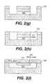
- FIGS. 2( a ) through 2 ( j )depict an exemplary process for forming n-type devices according to this invention.
- a patterned photo-resist layer 205is deposited over a silicon substrate 200 and the exposed portion of the silicon substrate 200 is doped, for example, with Ge, As, B, In or Sb.
- the doping concentration of Gemay be, for example, about 1 ⁇ 10 14 Ge/cm2 to about 1 ⁇ 10 16 Ge/cm2.
- a doped region 207is formed in the semiconductor substrate 200 .
- the patterned photo-resist layer 205is removed and a mask 210 , made of nitride, for example, is deposited on the surface of the semiconductor substrate 200 .
- the mask 210protects the semiconductor substrate beneath it from being etched during reactive ion etching (RIE). Generally, the mask 210 exposes portions of the semiconductor substrate where shallow trenches are to be formed via RIE.
- RIEreactive ion etching
- RIEis performed to form grooves/trenches 215 in the semiconductor substrate 200 .
- side-wall portions 217 of the doped semiconductor regionare formed.
- the location of the formed grooves/trenchesat least partially overlaps a portion of the doped semiconductor region 207 such that when the grooves/trenches 215 are formed, the doped semiconductor substrate region is exposed.
- oxide materialis deposited to fill the trenches, such that devices adjacent to each other on the semiconductor substrate 200 are electrically isolated from each other.
- wet etching and/or dry etchingis performed to selectively remove the doped semiconductor 207 .
- the depth of the trenchwill be about 1000 Angstroms to about 5000 Angstroms from the upper surface 231 ( FIG. 2( f )) of the semiconductor substrate and the thickness of a channel region of a transistor is typically about 30 Angstroms to about 200 Angstroms.
- etchingmay be performed until a tunnel-like gap 219 is formed between an upper portion 221 of the semiconductor substrate 200 and a lower portion 223 of the semiconductor substrate 200 .
- a portion having a depth of about 300 Angstroms to about 5000 Angstromsis etched from the semiconductor substrate 200 .
- a spacer material 225is deposited over the semiconductor substrate 200 .
- the spacer materialmay be, for example, a non-conformal film such as, silicon carbide SiC, oxynitride or a film stack, such as, an oxide film and a nitride film.
- This spacer material 225is formed on the exposed portions of the semiconductor substrate 200 other than the portion of the semiconductor substrate below the upper portion 221 .
- a strain layer 227is epitaxially grown in the tunnel-like gap 219 of the semiconductor substrate 200 .
- the strain layer 227is generally formed between an upper portion 221 and a lower portion 223 of the semiconductor substrate 200 , where the upper portion 221 of the semiconductor substrate 200 is part of the original semiconductor substrate (i.e., was not removed/disturbed and deposited). That is, the strain layer 227 is generally formed via selective deposition such that the strain layer 227 is formed on the exposed surfaces of the semiconductor substrate 200 .
- the strain layer 227is formed in a tunnel-like gap, the upper surface 231 of the upper portion 221 is undisturbed (i.e., original) and substantially flat.
- the strain layermay be, for example, silicon germanium or silicon carbide. It should be understood that the strain layer may be made of any known appropriate material.
- the spacer material 225is removed using wet chemicals. It should be understood that any known applicable method may be used to remove the spacer material 225 . The resulting device without the spacer material is shown in FIG. 2( g ).
- oxide material 233is then deposited to fill the trenches and electrically isolate the device from any adjacent device.
- the mask 210is removed using any known appropriate method.
- CMPchemical mechanical polishing
- a gate oxide layer 235is grown on the upper surface 231 of the semiconductor substrate 200 .
- a gate oxide layer 235 of about 10 Angstoms to about 100 ⁇is generally grown.
- a polysilicon layer 236is generally deposited using chemical vapor deposition (CVD) to a thickness of about 500 Angstoms to about 1500 Angstoms to form the gate electrode 237 .
- Patterned photoresist layersare used to define the gate electrodes.
- a thin layer of oxide(not oxide) is then grown on the remaining polysilicon.
- Patterned photoresist layers(not shown), which are later removed, are used to successively tip (and halo countering doping implants) implant the n-type and p-type transistors.
- a very shallow and low dose implant of arsenic ionsfor example, may be used to form the p-tip (while a Boron implant, for example, may be used for halos).
- a very shallow and low dose implant of BF.sub.2 ionsfor example, may be used to form n-tip (while an arsenic implant may, for example, be used for halos).
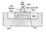
- spacers 238may be are formed by depositing a silicon nitride layer (not shown) using CVD to a thickness of about 100 Angstoms to about 1000 Angstoms and then etching the nitride from the regions other than the sidewalls of the gate.
- the combination of the gate oxide layer 235 , gate electrode 237 and spacers 238may be referred to as a gate stack.
- Patterned photoresist layers(not shown), which are removed prior to the next stage of the process, are used to successively create the source/drain regions of the transistors.
- a shallow and high-dose of arsenic ionsfor example, may be used to form the source/drain regions 240 and 241 while the p-type transistors are covered with the corresponding photoresist layer.
- the source and drain regions 240 and 241are formed in upper portions of semiconductor substrate 200 (i.e., not removed and reformed).
- the p-type transistorsdiscussed below with regards to FIGS.
- a shallow and high dose of BF 2 ionsmay be used to form the source/drain regions 340 and 341 while the n-type transistors are covered with the corresponding photoresist layer.
- An annealis then used to activate the implants.
- the exposed oxide on the structureis then stripped by dipping the structure in HF in order to expose bare silicon in the source, gate and drain regions of the transistors.
- metalis deposited to a thickness of about 30 Angstroms to about 200 Angstroms across the wafer surface in order to form silicide 242 .
- the silicidecould be formed from reacting the underlying with any deposited metal such as Co, Hf, Mo, Ni, Pd2, Pt, Ta, Ti, W, and Zr.
- the deposited metalreacts with the silicon to form silicide.
- the structureis heated to temperature of about 300° C. to about 1000° C. to allow the deposited silicide material to react with the exposed polysilicon or silicon.
- silicideonly forms in the regions where metal is in direct contact with silicon or polysilicon. In the other regions (i.e., where the deposited metal is not in contact with silicon), the deposited metal remains unchanged. This process aligns the silicide to the exposed silicon and is called “self-aligned silicide” or salicide. The unreacted metal is then removed using a wet etch while the formed suicide remains.
- the surfaceis more favorable to cobalt silicide formation as cobalt silicide.
- an oxide fill(not shown) followed by chemical mechanical polishing is used to planarize the surface. The fabrication processes continues as necessary according to the design specifications.
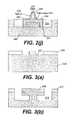
- FIGS. 3( a ) through 3 ( d )depict an exemplary process for forming p-type devices according to this invention.
- the process for forming p-type devicesis similar to the process for forming n-type devices, as discussed above with regards to FIGS. 2( a ) 2 ( j ) and thus, the following discussion will primarily focus on the differences between the two process.
- the details of the method for forming a p-type devicewhich are not discussed below, may be found in the above description of the method for forming an n-type device.
- a patterned photo-resist layer 305is deposited.
- the portion 307 of the semiconductor substrate 300 which will be below the channel of the semiconductor deviceis also covered with the patterned photo-resist layer 305 .
- a portion 308 of the semiconductor substrate 300remains. After the structure is formed, this portion 308 of the semiconductor substrate is substantially directly under the channel of the semiconductor device.
- a strain layer 327is grown in the gap between the remaining upper portion 301 and lower portion 302 of the semiconductor substrate 300 .
- oxide materialis deposited to fill the gaps/trenches 315 .
- gate oxide 335is deposited on the upper surface of the semiconductor substrate and the gate electrode 337 , spacers 338 , source/drain regions 340 and 341 and silicide contacts 342 are formed.
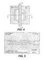
- FIG. 4depicts a top-down view of a transistor according to the invention.
- a cross-sectional view taken along line A-A of FIG. 4is the structure shown in FIG. 2(I) and a cross-sectional view taken along line B-B of FIG. 4 is the structure shown in FIG. 2( j ).
- the gate electrode 237 with the spacer 238is located above the semiconductor substrate 200 .
- the oxide fill 233i.e., shallow trench isolation structure isolates the source and drain regions 240 and 241 of the semiconductor substrate 200 .
- FIG. 5shows a cross-section of a semiconductor substrate according to the invention.
- the representation of the semiconductor substrate shown in FIG. 5was obtained using a scanning electron microscope.
- FIG. 5shows the silicon substrate after the doped silicon has been selectively removed to form tunnel-like gaps 219 in the semiconductor substrate.
- a lower surface of an upper portion of the semiconductor substrate and an upper surface of a lower portion of the semiconductor substratedefine a portion of the gap in the semiconductor substrate.
- the gap in the semiconductor substratemay include an opening along an upper surface of the semiconductor substrate.
- a longitudinal compressive stressis desired.
- the typical range for the desired compressive/tensile stressesis on the order of a few hundred MPa to a few GPa. For example, stresses of about 100 MPa to about 2 or 3 GPa are generally desired.
- the inventioncan produce very high compressive stresses and tensile stresses in the channels of the PFET and NFET devices, respectively.
- the inventionprovides a method for providing compressive stresses along the longitudinal direction of the channel by providing a strain layer either substantially directly under the channel of the semiconductor device or substantially directly under the source and/or drain region of the semiconductor device.
- This inventionalso provides a method for optimizing the stress level in the transistor channel by adjusting the location and/depth of the gap where the strain layer is formed.
Landscapes
- Engineering & Computer Science (AREA)
- Physics & Mathematics (AREA)
- Computer Hardware Design (AREA)
- Power Engineering (AREA)
- Microelectronics & Electronic Packaging (AREA)
- Condensed Matter Physics & Semiconductors (AREA)
- General Physics & Mathematics (AREA)
- Manufacturing & Machinery (AREA)
- High Energy & Nuclear Physics (AREA)
- Toxicology (AREA)
- Health & Medical Sciences (AREA)
- Spectroscopy & Molecular Physics (AREA)
- Chemical & Material Sciences (AREA)
- Materials Engineering (AREA)
- Insulated Gate Type Field-Effect Transistor (AREA)
- Metal-Oxide And Bipolar Metal-Oxide Semiconductor Integrated Circuits (AREA)
- Recrystallisation Techniques (AREA)
Abstract
Description
- The present application is a continuation of U.S. patent application Ser. No. 12/173,642, filed on Jul. 15, 2008, which is a continuation of U.S. patent application Ser. No. 11/534,526, filed on Sep. 22, 2006, now U.S. Pat. No. 7,429,752, which application is a continuation of parent U.S. patent application Ser. No. 10/605,906, filed on Nov. 5, 2003, now U.S. Pat. No. 7,129,126, the disclosures of these applications are expressly incorporated by reference herein in their entireties.
- The invention generally relates to methods for manufacturing a semiconductor device with improved device performance, and more particularly to methods for manufacturing semiconductor devices which impose tensile and compressive stresses in the substrate of the device during device fabrication.
- Generally, metal-oxide semiconductor transistors include a substrate made of a semiconductor material, such as silicon. The transistors typically include a source region, a channel region and a drain region within the substrate. The channel region is located between the source and the drain regions. A gate stack, which usually includes a conductive material, a gate oxide layer and sidewall spacers, is generally provided above the channel region. More particularly, the gate oxide layer is typically provided on the substrate over the channel region, while the gate conductor is usually provided above the gate oxide layer. The sidewall spacers help protect the sidewalls of the gate conductor.
- It is known that the amount of current flowing through a channel which has a given electric field across it, is generally directly proportional to the mobility of the carriers in the channel. Thus, by increasing the mobility of the carriers in the channel, the operation speed of the transistor can be increased.
- It is further known that mechanical stresses within a semiconductor device substrate can modulate device performance by, for example, increasing the mobility of the carriers in the semiconductor device. That is, stresses within a semiconductor device are known to enhance semiconductor device characteristics. Thus, to improve the characteristics of a semiconductor device, tensile and/or compressive stresses are created in the channel of the n-type devices (e.g., NFETs) and/or p-type devices (e.g., PFETs). However, the same stress component, for example tensile stress or compressive stress, improves the device characteristics of one type of device (i.e., n-type device or p-type device) while discriminatively affecting the characteristics of the other type device.
- In order to maximize the performance of both NFETs and PFETs within integrated circuit (IC) devices, the stress components should be engineered and applied differently for NFETs and PFETs. That is, because the type of stress which is beneficial for the performance of an NFET is generally disadvantageous for the performance of the PFET. More particularly, when a device is in tension (in the direction of current flow in a planar device), the performance characteristics of the NFET are enhanced while the performance characteristics of the PFET are diminished. To selectively create tensile stress in an NFET and compressive stress in a PFET, distinctive processes and different combinations of materials are used.
- For example, a trench isolation structure has been proposed for forming the appropriate stresses in the NFETs and PFETs, respectively. When this method is used, the isolation region for the NFET device contains a first isolation material which applies a first type of mechanical stress on the NFET device in a longitudinal direction (parallel to the direction of current flow) and in a transverse direction (perpendicular to the direction of current flow). Further, a first isolation region and a second isolation region are provided for the PFET and each of the isolation regions of the PFET device applies a unique mechanical stress on the PFET device in the transverse and longitudinal directions.
- Alternatively, liners on gate sidewalls have been proposed to selectively induce the appropriate strain in the channels of the FET devices (see Ootsuka et al., IEDM 2000, p. 575, for example). By providing liners the appropriate stress is applied closer to the device that the stress applies as a result of the trench isolation fill technique.
- While these methods do provide structures that have tensile stresses being applied to the NFET device and the compressive stresses being applied along the longitudinal direction of the PFET device, they may require additional materials and/or more complex processing, and thus, resulting in higher cost. Further, the level of stress that can be applied in these situations is typically moderate (i.e., on the order of 100 s of MPa). Thus, it is desired to provide more cost-effective and simplified methods for creating large tensile and compressive stresses in the channels NFETs and PFETs, respectively.
- In a first aspect of the invention, the invention provides a method for manufacturing a device including an n-type device and a p-type device. The method involves doping a portion of a semiconductor substrate and forming a gap in the semiconductor substrate by removing at least a portion of the doped portion of the semiconductor substrate. The method further involves growing a strain layer in at least a portion of the gap in the semiconductor substrate.
- In aspects of the invention, for the n-type device, the strain layer is grown on at least a portion which is substantially directly under a channel of the n-type device. For the p-type device, the strain layer is grown on at least a portion which is substantially directly under a source region or drain region of the p-type device and not substantially under a channel of the p-type device.
- In another aspect of the invention, the invention provides a method for manufacturing a device including an n-type device and a p-type device. The method involves growing a strain layer on a semiconductor substrate and growing a silicon layer above the strain layer. A gap is formed between the semiconductor substrate and the silicon layer by removing at least a portion of the silicon layer and the strain layer from above the semiconductor substrate and a strain layer is grown in at least a portion of the gap. For the n-type device, the strain layer is grown on at least a portion which is substantially directly under a channel of the n-type device. For the p-type device, the strain layer is grown on at least a portion which is substantially directly under a source region or drain region of the p-type device and not substantially under a channel of the p-type device.
- This invention separately provides a semiconductor device which has a semiconductor substrate having at least one gap, the gap extending under a portion of the semiconductor substrate. The device includes a gate stack on the semiconductor substrate and a strain layer formed in at least a portion of the gap, where the gap is formed by doping a portion of the semiconductor substrate and etching the doped portions of the semiconductor substrate.
- In another aspect of the invention, the invention provides a semiconductor device which has a semiconductor substrate having at least one gap, the gap extending under a portion of the semiconductor substrate. The device includes a gate stack on the semiconductor substrate and a strain layer formed only under at least a portion of a source region and a drain region of the semiconductor substrate.
FIG. 1 illustrates desired stress states for PFETs and NFETs;FIGS. 2( a) through2(j) illustrate an exemplary process for forming a n-type transistor according to the invention;FIGS. 3( a) through3(d) illustrate an exemplary process for forming an p-type transistor according to the invention;FIG. 4 illustrates a top-down view of a transistor according to the invention; andFIG. 5 shows a cross-section of a semiconductor substrate according to the invention using a scanning electron microscope.- The invention provides a method for fabricating devices with improved performance characteristics. When a stress layer, such as, a SiGe layer, a Si3N4layer, a SiO2layer or a SiOxNylayer is grown epitaxially on a silicon layer, compressive forces form within the SiGe layer and tensile forces form in the silicon layer. In an aspect of the invention, the silicon substrate has a gap in which a strain layer is grown. The gap includes a tunnel-like portion which is between an upper portion of the semiconductor substrate and a lower portion of the semiconductor substrate. More particularly, the upper portion has a lower surface and the lower portion face has an upper surface and the lower surface of the upper portion faces the upper surface of the lower portion. By having a strain layer substantially below a channel and/or a strain layer in a region of the semiconductor substrate substantially below a source region and/or a drain region of the semiconductor device stresses are formed in the channel of the transistor. In an aspect of the invention, the gap in the silicon substrate is formed by selectively etching the silicon substrate and then epitaxially growing SiGe on the silicon substrate.
- Tensile and/or compressive stresses can be provided in the channel of a transistor depending on the proximity of the grown SiGe to the channel of the transistor. By selectively etching the silicon layer below a transistor and selectively growing SiGe on the etched portion of the silicon layer, tensile stresses can be provided in the channel of NFETs and compressive stresses can be provided in the channel of PFETs. Further, by implementing the stresses by selectively etching a portion of the silicon below a transistor prior to growing SiGe, this invention provides stress levels in the silicon under the gate (e.g., the channel region) which are much larger than the isolation-based or liner-based approaches.
- In this invention, a stress layer, such as a SiGe layer, for example, is used to form stresses in a channel of the semiconductor device. When a SiGe layer is grown on a semiconductor layer the surrounding semiconductor material is subjected to tensile stress while the grown SiGe layer is subjected to compressive stress. In particular, a portion of the semiconductor device is put under tensile stress and the SiGe layer is subjected to compressive stress because the SiGe layer has a different lattice structure than the silicon layer. Further, the stress levels resulting from the SiGe stress layer are relatively high (on the order of 1-2 GPa).
- However, as discussed above, tensile stresses in the channel area are beneficial to the NFET drive currents while compressive stresses in the channel area are beneficial to the PFET drive currents. In particular, tensile stresses significantly hinder the PFET drive currents. In this invention, the stresses in the PFET are made to be compressive stresses rather than tensile stresses in order to improve the performance of the PFET. Thus, this invention provides a method for providing longitudinal compressive stresses along the channel of the PFET while providing tensile stresses along the channel of the NFET to improve the performance of the devices.
FIG. 1 illustrates desired stress states for improving the performance of PFETs and NFETs (see Wang et al., IEEE Tran. Electron Dev., v. 50, p. 529, 2003). InFIG. 1 , an NFET and a PFET are shown to have a source region, a gate region and a drain region. The NFET and PFET are shown to have arrows extending outward from the active area to illustrate tensile stresses. The arrows extending inward toward the PFET device are illustrative of compressive forces. More specifically, the outwardly extending arrows, shown extending from the NFET, illustrate a tensile stress that is desired in the transverse and longitudinal directions of the device. On the other hand, the inwardly extending arrows, shown with relation to the PFET, illustrate a desired longitudinal compressive stress.- The range of stresses needed to influence device drive currents is of the order of a few hundred MPa to a few GPa. The width and the length of the active area of each device are represented by “W” and “L”, respectively. It should be understood that each of the longitudinal or transverse stress components could be individually tailored to provide the performance enhancements for both devices (i.e., the NFET and the PFET).
FIGS. 2( a) through2(j) depict an exemplary process for forming n-type devices according to this invention. As shown inFIG. 2( a), a patterned photo-resistlayer 205 is deposited over asilicon substrate 200 and the exposed portion of thesilicon substrate 200 is doped, for example, with Ge, As, B, In or Sb. For example, the doping concentration of Ge may be, for example, about 1×10¹⁴Ge/cm2 to about 1×10¹⁶Ge/cm2. A dopedregion 207 is formed in thesemiconductor substrate 200.- Then, as shown in
FIG. 2( b), the patterned photo-resistlayer 205 is removed and amask 210, made of nitride, for example, is deposited on the surface of thesemiconductor substrate 200. Themask 210 protects the semiconductor substrate beneath it from being etched during reactive ion etching (RIE). Generally, themask 210 exposes portions of the semiconductor substrate where shallow trenches are to be formed via RIE. - As shown in
FIG. 2( c), RIE is performed to form grooves/trenches 215 in thesemiconductor substrate 200. As a result of the RIE step, side-wall portions 217 of the doped semiconductor region are formed. In particular, the location of the formed grooves/trenches at least partially overlaps a portion of the dopedsemiconductor region 207 such that when the grooves/trenches 215 are formed, the doped semiconductor substrate region is exposed. Further, as will be discussed below, after a strain layer is formed, oxide material is deposited to fill the trenches, such that devices adjacent to each other on thesemiconductor substrate 200 are electrically isolated from each other. - After the grooves/
trenches 215 are formed, wet etching and/or dry etching is performed to selectively remove the dopedsemiconductor 207. Generally, the depth of the trench will be about 1000 Angstroms to about 5000 Angstroms from the upper surface231 (FIG. 2( f)) of the semiconductor substrate and the thickness of a channel region of a transistor is typically about 30 Angstroms to about 200 Angstroms. - As shown in
FIG. 2( d), etching may be performed until a tunnel-like gap 219 is formed between anupper portion 221 of thesemiconductor substrate 200 and alower portion 223 of thesemiconductor substrate 200. Typically, a portion having a depth of about 300 Angstroms to about 5000 Angstroms is etched from thesemiconductor substrate 200. In the case of an n-type transistor it is desired to form the strain layer substantially directly and/or directly under the channel of the device. Thus, for n-type transistors there is at least a gap under the channel of the device. - Next, as shown in
FIG. 2( e), aspacer material 225 is deposited over thesemiconductor substrate 200. The spacer material may be, for example, a non-conformal film such as, silicon carbide SiC, oxynitride or a film stack, such as, an oxide film and a nitride film. Thisspacer material 225 is formed on the exposed portions of thesemiconductor substrate 200 other than the portion of the semiconductor substrate below theupper portion 221. - As shown in
FIG. 2( f), astrain layer 227 is epitaxially grown in the tunnel-like gap 219 of thesemiconductor substrate 200. As shown inFIG. 2( f), thestrain layer 227 is generally formed between anupper portion 221 and alower portion 223 of thesemiconductor substrate 200, where theupper portion 221 of thesemiconductor substrate 200 is part of the original semiconductor substrate (i.e., was not removed/disturbed and deposited). That is, thestrain layer 227 is generally formed via selective deposition such that thestrain layer 227 is formed on the exposed surfaces of thesemiconductor substrate 200. - Further, because the
strain layer 227 is formed in a tunnel-like gap, theupper surface 231 of theupper portion 221 is undisturbed (i.e., original) and substantially flat. - The strain layer may be, for example, silicon germanium or silicon carbide. It should be understood that the strain layer may be made of any known appropriate material.
- After the
strain layer 227 is formed, thespacer material 225 is removed using wet chemicals. It should be understood that any known applicable method may be used to remove thespacer material 225. The resulting device without the spacer material is shown inFIG. 2( g). - As discussed above, and as shown in
FIG. 2( h),oxide material 233 is then deposited to fill the trenches and electrically isolate the device from any adjacent device. After filling the trenches with the oxide material, themask 210 is removed using any known appropriate method. After themask 210 is removed, chemical mechanical polishing (CMP) is performed to substantially planarize theupper surface 231 of thesemiconductor substrate 200. - Next, the semiconductor device is further fabricated using known methods. For example, as shown in
FIG. 2(I) , agate oxide layer 235 is grown on theupper surface 231 of thesemiconductor substrate 200. Agate oxide layer 235 of about 10 Angstoms to about 100 Å is generally grown. On thegate oxide layer 235, apolysilicon layer 236 is generally deposited using chemical vapor deposition (CVD) to a thickness of about 500 Angstoms to about 1500 Angstoms to form thegate electrode 237. Patterned photoresist layers (not shown) are used to define the gate electrodes. A thin layer of oxide (not oxide) is then grown on the remaining polysilicon. Patterned photoresist layers (not shown), which are later removed, are used to successively tip (and halo countering doping implants) implant the n-type and p-type transistors. For n-type transistors, a very shallow and low dose implant of arsenic ions, for example, may be used to form the p-tip (while a Boron implant, for example, may be used for halos). For p-type transistors, (discussed below with regards toFIGS. 3( a)3(d)), a very shallow and low dose implant of BF.sub.2 ions, for example, may be used to form n-tip (while an arsenic implant may, for example, be used for halos). - Next, as shown in
FIG. 2( j),spacers 238 may be are formed by depositing a silicon nitride layer (not shown) using CVD to a thickness of about 100 Angstoms to about 1000 Angstoms and then etching the nitride from the regions other than the sidewalls of the gate. The combination of thegate oxide layer 235,gate electrode 237 andspacers 238 may be referred to as a gate stack. - Patterned photoresist layers (not shown), which are removed prior to the next stage of the process, are used to successively create the source/drain regions of the transistors. For the n-type transistors, a shallow and high-dose of arsenic ions, for example, may be used to form the source/
drain regions regions FIGS. 3( a)-3(d)), a shallow and high dose of BF2ions, for example, may be used to form the source/drain regions - Still referring to
FIG. 2( j), metal is deposited to a thickness of about 30 Angstroms to about 200 Angstroms across the wafer surface in order to formsilicide 242. The silicide could be formed from reacting the underlying with any deposited metal such as Co, Hf, Mo, Ni, Pd2, Pt, Ta, Ti, W, and Zr. In the regions, such as, the source, drain and gate regions, where the deposited metal is in contact with silicon, the deposited metal reacts with the silicon to form silicide. Next, the structure is heated to temperature of about 300° C. to about 1000° C. to allow the deposited silicide material to react with the exposed polysilicon or silicon. During sintering, silicide only forms in the regions where metal is in direct contact with silicon or polysilicon. In the other regions (i.e., where the deposited metal is not in contact with silicon), the deposited metal remains unchanged. This process aligns the silicide to the exposed silicon and is called “self-aligned silicide” or salicide. The unreacted metal is then removed using a wet etch while the formed suicide remains. - In the methods according to this invention because the source and drain regions of the semiconductor device are formed on portions of the semiconductor substrate which are undisturbed (i.e., not etched and re-formed), the surface is more favorable to cobalt silicide formation as cobalt silicide. Further, generally an oxide fill (not shown) followed by chemical mechanical polishing is used to planarize the surface. The fabrication processes continues as necessary according to the design specifications.
FIGS. 3( a) through3(d) depict an exemplary process for forming p-type devices according to this invention. The process for forming p-type devices is similar to the process for forming n-type devices, as discussed above with regards toFIGS. 2( a)2(j) and thus, the following discussion will primarily focus on the differences between the two process. The details of the method for forming a p-type device which are not discussed below, may be found in the above description of the method for forming an n-type device.- As shown in
FIG. 3( a), a patterned photo-resistlayer 305 is deposited. For the p-type devices, theportion 307 of thesemiconductor substrate 300 which will be below the channel of the semiconductor device is also covered with the patterned photo-resistlayer 305. Thus, for the p-type devices, as shown inFIG. 3( b), when the doped region of the semiconductor substrate is selectively etched to form thegap 315, aportion 308 of thesemiconductor substrate 300 remains. After the structure is formed, thisportion 308 of the semiconductor substrate is substantially directly under the channel of the semiconductor device. - Next, as shown in
FIG. 3( c), astrain layer 327 is grown in the gap between the remainingupper portion 301 andlower portion 302 of thesemiconductor substrate 300. Then, as shown inFIG. 3( d), oxide material is deposited to fill the gaps/trenches 315. Similar to the process for forming n-type devices,gate oxide 335 is deposited on the upper surface of the semiconductor substrate and thegate electrode 337,spacers 338, source/drain regions silicide contacts 342 are formed. FIG. 4 depicts a top-down view of a transistor according to the invention. A cross-sectional view taken along line A-A ofFIG. 4 is the structure shown inFIG. 2(I) and a cross-sectional view taken along line B-B ofFIG. 4 is the structure shown inFIG. 2( j). As shown inFIG. 4 , thegate electrode 237 with thespacer 238 is located above thesemiconductor substrate 200. The oxide fill233 (i.e., shallow trench isolation structure) isolates the source and drainregions semiconductor substrate 200.FIG. 5 shows a cross-section of a semiconductor substrate according to the invention. The representation of the semiconductor substrate shown inFIG. 5 was obtained using a scanning electron microscope. In particular,FIG. 5 shows the silicon substrate after the doped silicon has been selectively removed to form tunnel-like gaps 219 in the semiconductor substrate. As shown inFIG. 5 , a lower surface of an upper portion of the semiconductor substrate and an upper surface of a lower portion of the semiconductor substrate define a portion of the gap in the semiconductor substrate. The gap in the semiconductor substrate may include an opening along an upper surface of the semiconductor substrate.- In another embodiment of the methods according to this invention, instead of selectively doping the semiconductor substrate with Ge, for example, such that selective portions of the semiconductor substrate may be removed via etching, it is possible to grow a layer, such as, a SiGe layer, on the semiconductor substrate, followed by a silicon epitaxial layer, for example. Then, similar to the doping method described above, sidewalls of the SiGe may be exposed and then selectively etched to form the gaps in the semiconductor substrate.
- As discussed above with regards to
FIG. 1 , in PFETs, a longitudinal compressive stress is desired. The typical range for the desired compressive/tensile stresses is on the order of a few hundred MPa to a few GPa. For example, stresses of about 100 MPa to about 2 or 3 GPa are generally desired. The invention can produce very high compressive stresses and tensile stresses in the channels of the PFET and NFET devices, respectively. - By providing tensile stresses to the channel of the NFET and compressive stresses to the channel of the PFET the charge mobility along the channels of each device is enhanced. Thus, as described above, the invention provides a method for providing compressive stresses along the longitudinal direction of the channel by providing a strain layer either substantially directly under the channel of the semiconductor device or substantially directly under the source and/or drain region of the semiconductor device. This invention also provides a method for optimizing the stress level in the transistor channel by adjusting the location and/depth of the gap where the strain layer is formed.
- While the invention has been described in terms of embodiments, those skilled in the art will recognize that the invention can be practiced with modification within the spirit and scope of the appended claims.
Claims (16)
Priority Applications (1)
| Application Number | Priority Date | Filing Date | Title |
|---|---|---|---|
| US12/685,054US7928443B2 (en) | 2003-11-05 | 2010-01-11 | Method and structure for forming strained SI for CMOS devices |
Applications Claiming Priority (4)
| Application Number | Priority Date | Filing Date | Title |
|---|---|---|---|
| US10/605,906US7129126B2 (en) | 2003-11-05 | 2003-11-05 | Method and structure for forming strained Si for CMOS devices |
| US11/534,526US7429752B2 (en) | 2003-11-05 | 2006-09-22 | Method and structure for forming strained SI for CMOS devices |
| US12/173,642US7700951B2 (en) | 2003-11-05 | 2008-07-15 | Method and structure for forming strained Si for CMOS devices |
| US12/685,054US7928443B2 (en) | 2003-11-05 | 2010-01-11 | Method and structure for forming strained SI for CMOS devices |
Related Parent Applications (1)
| Application Number | Title | Priority Date | Filing Date |
|---|---|---|---|
| US12/173,642ContinuationUS7700951B2 (en) | 2003-11-05 | 2008-07-15 | Method and structure for forming strained Si for CMOS devices |
Publications (2)
| Publication Number | Publication Date |
|---|---|
| US20100109048A1true US20100109048A1 (en) | 2010-05-06 |
| US7928443B2 US7928443B2 (en) | 2011-04-19 |
Family
ID=34549690
Family Applications (5)
| Application Number | Title | Priority Date | Filing Date |
|---|---|---|---|
| US10/605,906Expired - Fee RelatedUS7129126B2 (en) | 2003-11-05 | 2003-11-05 | Method and structure for forming strained Si for CMOS devices |
| US11/534,526Expired - LifetimeUS7429752B2 (en) | 2003-11-05 | 2006-09-22 | Method and structure for forming strained SI for CMOS devices |
| US11/854,829Expired - Fee RelatedUS7550338B2 (en) | 2003-11-05 | 2007-09-13 | Method and structure for forming strained SI for CMOS devices |
| US12/173,642Expired - LifetimeUS7700951B2 (en) | 2003-11-05 | 2008-07-15 | Method and structure for forming strained Si for CMOS devices |
| US12/685,054Expired - Fee RelatedUS7928443B2 (en) | 2003-11-05 | 2010-01-11 | Method and structure for forming strained SI for CMOS devices |
Family Applications Before (4)
| Application Number | Title | Priority Date | Filing Date |
|---|---|---|---|
| US10/605,906Expired - Fee RelatedUS7129126B2 (en) | 2003-11-05 | 2003-11-05 | Method and structure for forming strained Si for CMOS devices |
| US11/534,526Expired - LifetimeUS7429752B2 (en) | 2003-11-05 | 2006-09-22 | Method and structure for forming strained SI for CMOS devices |
| US11/854,829Expired - Fee RelatedUS7550338B2 (en) | 2003-11-05 | 2007-09-13 | Method and structure for forming strained SI for CMOS devices |
| US12/173,642Expired - LifetimeUS7700951B2 (en) | 2003-11-05 | 2008-07-15 | Method and structure for forming strained Si for CMOS devices |
Country Status (6)
| Country | Link |
|---|---|
| US (5) | US7129126B2 (en) |
| EP (1) | EP1680804A4 (en) |
| JP (1) | JP4959337B2 (en) |
| KR (1) | KR100866826B1 (en) |
| CN (1) | CN100555600C (en) |
| WO (1) | WO2005045901A2 (en) |
Families Citing this family (24)
| Publication number | Priority date | Publication date | Assignee | Title |
|---|---|---|---|---|
| US7037770B2 (en)* | 2003-10-20 | 2006-05-02 | International Business Machines Corporation | Method of manufacturing strained dislocation-free channels for CMOS |
| US7129126B2 (en)* | 2003-11-05 | 2006-10-31 | International Business Machines Corporation | Method and structure for forming strained Si for CMOS devices |
| US7029964B2 (en)* | 2003-11-13 | 2006-04-18 | International Business Machines Corporation | Method of manufacturing a strained silicon on a SiGe on SOI substrate |
| US20050287747A1 (en)* | 2004-06-29 | 2005-12-29 | International Business Machines Corporation | Doped nitride film, doped oxide film and other doped films |
| US7176481B2 (en)* | 2005-01-12 | 2007-02-13 | International Business Machines Corporation | In situ doped embedded sige extension and source/drain for enhanced PFET performance |
| US7078285B1 (en)* | 2005-01-21 | 2006-07-18 | Sony Corporation | SiGe nickel barrier structure employed in a CMOS device to prevent excess diffusion of nickel used in the silicide material |
| US8972300B2 (en)* | 2006-04-27 | 2015-03-03 | Panasonic Corporation | Content distribution system |
| US7781839B2 (en)* | 2007-03-30 | 2010-08-24 | Freescale Semiconductor, Inc. | Structure and method for strained transistor directly on insulator |
| US7572689B2 (en)* | 2007-11-09 | 2009-08-11 | International Business Machines Corporation | Method and structure for reducing induced mechanical stresses |
| US7678634B2 (en)* | 2008-01-28 | 2010-03-16 | International Business Machines Corporation | Local stress engineering for CMOS devices |
| US8115194B2 (en)* | 2008-02-21 | 2012-02-14 | United Microelectronics Corp. | Semiconductor device capable of providing identical strains to each channel region of the transistors |
| FR2934416B1 (en)* | 2008-07-24 | 2011-09-02 | Inst Nat Sciences Appliq | CONSTRAINED SEMICONDUCTOR SUBSTRATE AND METHOD FOR MANUFACTURING THE SAME |
| US8368125B2 (en) | 2009-07-20 | 2013-02-05 | International Business Machines Corporation | Multiple orientation nanowires with gate stack stressors |
| US20110031503A1 (en)* | 2009-08-10 | 2011-02-10 | International Business Machines Corporation | Device with stressed channel |
| US8138523B2 (en)* | 2009-10-08 | 2012-03-20 | International Business Machines Corporation | Semiconductor device having silicon on stressed liner (SOL) |
| CN102315126A (en)* | 2010-07-07 | 2012-01-11 | 中国科学院微电子研究所 | Semiconductor device and manufacturing method thereof |
| US20130137235A1 (en)* | 2010-07-15 | 2013-05-30 | University Of Electronic Science And Technology Of China | Mos transistor using stress concentration effect for enhancing stress in channel area |
| CN104425280B (en)* | 2013-09-09 | 2018-08-14 | 中芯国际集成电路制造(上海)有限公司 | Semiconductor device structure and forming method thereof |
| US9368626B2 (en) | 2013-12-04 | 2016-06-14 | Taiwan Semiconductor Manufacturing Company, Ltd. | Semiconductor device with strained layer |
| US9515181B2 (en) | 2014-08-06 | 2016-12-06 | Qualcomm Incorporated | Semiconductor device with self-aligned back side features |
| GB201415119D0 (en)* | 2014-08-27 | 2014-10-08 | Ibm | Method for fabricating a semiconductor structure |
| US10079233B2 (en)* | 2016-09-28 | 2018-09-18 | International Business Machines Corporation | Semiconductor device and method of forming the semiconductor device |
| DE102019122987A1 (en) | 2019-08-27 | 2021-03-04 | Zf Airbag Germany Gmbh | Diffuser for a gas generator, gas generator with such a diffuser and manufacturing method for such a diffuser |
| US11502106B2 (en)* | 2020-02-11 | 2022-11-15 | Globalfoundries U.S. Inc. | Multi-layered substrates of semiconductor devices |
Citations (83)
| Publication number | Priority date | Publication date | Assignee | Title |
|---|---|---|---|---|
| US3602841A (en)* | 1970-06-18 | 1971-08-31 | Ibm | High frequency bulk semiconductor amplifiers and oscillators |
| US4665415A (en)* | 1985-04-24 | 1987-05-12 | International Business Machines Corporation | Semiconductor device with hole conduction via strained lattice |
| US4853076A (en)* | 1983-12-29 | 1989-08-01 | Massachusetts Institute Of Technology | Semiconductor thin films |
| US4855245A (en)* | 1985-09-13 | 1989-08-08 | Siemens Aktiengesellschaft | Method of manufacturing integrated circuit containing bipolar and complementary MOS transistors on a common substrate |
| US4952524A (en)* | 1989-05-05 | 1990-08-28 | At&T Bell Laboratories | Semiconductor device manufacture including trench formation |
| US4958213A (en)* | 1987-12-07 | 1990-09-18 | Texas Instruments Incorporated | Method for forming a transistor base region under thick oxide |
| US5006913A (en)* | 1988-11-05 | 1991-04-09 | Mitsubishi Denki Kabushiki Kaisha | Stacked type semiconductor device |
| US5060030A (en)* | 1990-07-18 | 1991-10-22 | Raytheon Company | Pseudomorphic HEMT having strained compensation layer |
| US5081513A (en)* | 1991-02-28 | 1992-01-14 | Xerox Corporation | Electronic device with recovery layer proximate to active layer |
| US5108843A (en)* | 1988-11-30 | 1992-04-28 | Ricoh Company, Ltd. | Thin film semiconductor and process for producing the same |
| US5134085A (en)* | 1991-11-21 | 1992-07-28 | Micron Technology, Inc. | Reduced-mask, split-polysilicon CMOS process, incorporating stacked-capacitor cells, for fabricating multi-megabit dynamic random access memories |
| US5241197A (en)* | 1989-01-25 | 1993-08-31 | Hitachi, Ltd. | Transistor provided with strained germanium layer |
| US5310446A (en)* | 1990-01-10 | 1994-05-10 | Ricoh Company, Ltd. | Method for producing semiconductor film |
| US5354695A (en)* | 1992-04-08 | 1994-10-11 | Leedy Glenn J | Membrane dielectric isolation IC fabrication |
| US5391510A (en)* | 1992-02-28 | 1995-02-21 | International Business Machines Corporation | Formation of self-aligned metal gate FETs using a benignant removable gate material during high temperature steps |
| US5459346A (en)* | 1988-06-28 | 1995-10-17 | Ricoh Co., Ltd. | Semiconductor substrate with electrical contact in groove |
| US5557122A (en)* | 1995-05-12 | 1996-09-17 | Alliance Semiconductors Corporation | Semiconductor electrode having improved grain structure and oxide growth properties |
| US5561302A (en)* | 1994-09-26 | 1996-10-01 | Motorola, Inc. | Enhanced mobility MOSFET device and method |
| US5670798A (en)* | 1995-03-29 | 1997-09-23 | North Carolina State University | Integrated heterostructures of Group III-V nitride semiconductor materials including epitaxial ohmic contact non-nitride buffer layer and methods of fabricating same |
| US5679965A (en)* | 1995-03-29 | 1997-10-21 | North Carolina State University | Integrated heterostructures of Group III-V nitride semiconductor materials including epitaxial ohmic contact, non-nitride buffer layer and methods of fabricating same |
| US5861651A (en)* | 1997-02-28 | 1999-01-19 | Lucent Technologies Inc. | Field effect devices and capacitors with improved thin film dielectrics and method for making same |
| US5880040A (en)* | 1996-04-15 | 1999-03-09 | Macronix International Co., Ltd. | Gate dielectric based on oxynitride grown in N2 O and annealed in NO |
| US5940736A (en)* | 1997-03-11 | 1999-08-17 | Lucent Technologies Inc. | Method for forming a high quality ultrathin gate oxide layer |
| US5960297A (en)* | 1997-07-02 | 1999-09-28 | Kabushiki Kaisha Toshiba | Shallow trench isolation structure and method of forming the same |
| US5989978A (en)* | 1998-07-16 | 1999-11-23 | Chartered Semiconductor Manufacturing, Ltd. | Shallow trench isolation of MOSFETS with reduced corner parasitic currents |
| US6025280A (en)* | 1997-04-28 | 2000-02-15 | Lucent Technologies Inc. | Use of SiD4 for deposition of ultra thin and controllable oxides |
| US6066545A (en)* | 1997-12-09 | 2000-05-23 | Texas Instruments Incorporated | Birdsbeak encroachment using combination of wet and dry etch for isolation nitride |
| US6090684A (en)* | 1998-07-31 | 2000-07-18 | Hitachi, Ltd. | Method for manufacturing semiconductor device |
| US6107143A (en)* | 1998-03-02 | 2000-08-22 | Samsung Electronics Co., Ltd. | Method for forming a trench isolation structure in an integrated circuit |
| US6117722A (en)* | 1999-02-18 | 2000-09-12 | Taiwan Semiconductor Manufacturing Company | SRAM layout for relaxing mechanical stress in shallow trench isolation technology and method of manufacture thereof |
| US6133071A (en)* | 1997-10-15 | 2000-10-17 | Nec Corporation | Semiconductor device with plate heat sink free from cracks due to thermal stress and process for assembling it with package |
| US6221735B1 (en)* | 2000-02-15 | 2001-04-24 | Philips Semiconductors, Inc. | Method for eliminating stress induced dislocations in CMOS devices |
| US6228694B1 (en)* | 1999-06-28 | 2001-05-08 | Intel Corporation | Method of increasing the mobility of MOS transistors by use of localized stress regions |
| US20010003364A1 (en)* | 1998-05-27 | 2001-06-14 | Sony Corporation | Semiconductor and fabrication method thereof |
| US6255169B1 (en)* | 1999-02-22 | 2001-07-03 | Advanced Micro Devices, Inc. | Process for fabricating a high-endurance non-volatile memory device |
| US6261964B1 (en)* | 1997-03-14 | 2001-07-17 | Micron Technology, Inc. | Material removal method for forming a structure |
| US6265317B1 (en)* | 2001-01-09 | 2001-07-24 | Taiwan Semiconductor Manufacturing Company | Top corner rounding for shallow trench isolation |
| US20010009784A1 (en)* | 1998-01-09 | 2001-07-26 | Yanjun Ma | Structure and method of making a sub-micron MOS transistor |
| US6274444B1 (en)* | 1999-07-30 | 2001-08-14 | United Microelectronics Corp. | Method for forming mosfet |
| US6281532B1 (en)* | 1999-06-28 | 2001-08-28 | Intel Corporation | Technique to obtain increased channel mobilities in NMOS transistors by gate electrode engineering |
| US6284626B1 (en)* | 1999-04-06 | 2001-09-04 | Vantis Corporation | Angled nitrogen ion implantation for minimizing mechanical stress on side walls of an isolation trench |
| US6284623B1 (en)* | 1999-10-25 | 2001-09-04 | Peng-Fei Zhang | Method of fabricating semiconductor devices using shallow trench isolation with reduced narrow channel effect |
| US6319794B1 (en)* | 1998-10-14 | 2001-11-20 | International Business Machines Corporation | Structure and method for producing low leakage isolation devices |
| US20010045604A1 (en)* | 2000-05-25 | 2001-11-29 | Hitachi, Ltd. | Semiconductor device and manufacturing method |
| US6361885B1 (en)* | 1998-04-10 | 2002-03-26 | Organic Display Technology | Organic electroluminescent materials and device made from such materials |
| US6362082B1 (en)* | 1999-06-28 | 2002-03-26 | Intel Corporation | Methodology for control of short channel effects in MOS transistors |
| US6368931B1 (en)* | 2000-03-27 | 2002-04-09 | Intel Corporation | Thin tensile layers in shallow trench isolation and method of making same |
| US20020063292A1 (en)* | 2000-11-29 | 2002-05-30 | Mark Armstrong | CMOS fabrication process utilizing special transistor orientation |
| US6403975B1 (en)* | 1996-04-09 | 2002-06-11 | Max-Planck Gesellschaft Zur Forderung Der Wissenschafteneev | Semiconductor components, in particular photodetectors, light emitting diodes, optical modulators and waveguides with multilayer structures grown on silicon substrates |
| US6403486B1 (en)* | 2001-04-30 | 2002-06-11 | Taiwan Semiconductor Manufacturing Company | Method for forming a shallow trench isolation |
| US6406973B1 (en)* | 1999-06-29 | 2002-06-18 | Hyundai Electronics Industries Co., Ltd. | Transistor in a semiconductor device and method of manufacturing the same |
| US20020086472A1 (en)* | 2000-12-29 | 2002-07-04 | Brian Roberds | Technique to obtain high mobility channels in MOS transistors by forming a strain layer on an underside of a channel |
| US20020086497A1 (en)* | 2000-12-30 | 2002-07-04 | Kwok Siang Ping | Beaker shape trench with nitride pull-back for STI |
| US20020090791A1 (en)* | 1999-06-28 | 2002-07-11 | Brian S. Doyle | Method for reduced capacitance interconnect system using gaseous implants into the ild |
| US6423615B1 (en)* | 1999-09-22 | 2002-07-23 | Intel Corporation | Silicon wafers for CMOS and other integrated circuits |
| US6461936B1 (en)* | 2002-01-04 | 2002-10-08 | Infineon Technologies Ag | Double pullback method of filling an isolation trench |
| US6506652B2 (en)* | 1998-11-13 | 2003-01-14 | Intel Corporation | Method of recessing spacers to improved salicide resistance on polysilicon gates |
| US20030032261A1 (en)* | 2001-08-08 | 2003-02-13 | Ling-Yen Yeh | Method of preventing threshold voltage of MOS transistor from being decreased by shallow trench isolation formation |
| US20030032661A1 (en)* | 2001-08-02 | 2003-02-13 | Boehringer Ingelheim Pharma Kg | Pramipexole as an anticonvulsant |
| US20030040158A1 (en)* | 2001-08-21 | 2003-02-27 | Nec Corporation | Semiconductor device and method of fabricating the same |
| US6531369B1 (en)* | 2000-03-01 | 2003-03-11 | Applied Micro Circuits Corporation | Heterojunction bipolar transistor (HBT) fabrication using a selectively deposited silicon germanium (SiGe) |
| US6531740B2 (en)* | 2001-07-17 | 2003-03-11 | Motorola, Inc. | Integrated impedance matching and stability network |
| US20030057184A1 (en)* | 2001-09-22 | 2003-03-27 | Shiuh-Sheng Yu | Method for pull back SiN to increase rounding effect in a shallow trench isolation process |
| US20030067035A1 (en)* | 2001-09-28 | 2003-04-10 | Helmut Tews | Gate processing method with reduced gate oxide corner and edge thinning |
| US20030087492A1 (en)* | 2001-11-02 | 2003-05-08 | Promos Technologies, Inc. | Semiconductor device and method of manufacturing the same |
| US20030086472A1 (en)* | 1999-12-15 | 2003-05-08 | Daniel Bengtsson | Method and device for the measuring of the optical power loss in a fiber optical contact means |
| US6703648B1 (en)* | 2002-10-29 | 2004-03-09 | Advanced Micro Devices, Inc. | Strained silicon PMOS having silicon germanium source/drain extensions and method for its fabrication |
| US6703293B2 (en)* | 2002-07-11 | 2004-03-09 | Sharp Laboratories Of America, Inc. | Implantation at elevated temperatures for amorphization re-crystallization of Si1-xGex films on silicon substrates |
| US6717216B1 (en)* | 2002-12-12 | 2004-04-06 | International Business Machines Corporation | SOI based field effect transistor having a compressive film in undercut area under the channel and a method of making the device |
| US6787423B1 (en)* | 2002-12-09 | 2004-09-07 | Advanced Micro Devices, Inc. | Strained-silicon semiconductor device |
| US20040188760A1 (en)* | 2002-04-03 | 2004-09-30 | Thomas Skotnicki | Strained-channel isolated-gate field effect transistor, process for making same and resulting integrated circuit |
| US20050040460A1 (en)* | 2002-12-12 | 2005-02-24 | Dureseti Chidambarrao | Stress inducing spacers |
| US20050082634A1 (en)* | 2003-10-16 | 2005-04-21 | International Business Machines Corporation | High performance strained cmos devices |
| US20050093030A1 (en)* | 2003-10-30 | 2005-05-05 | Doris Bruce B. | Structure and method to enhance both nFET and pFET performance using different kinds of stressed layers |
| US6891192B2 (en)* | 2003-08-04 | 2005-05-10 | International Business Machines Corporation | Structure and method of making strained semiconductor CMOS transistors having lattice-mismatched semiconductor regions underlying source and drain regions |
| US20050098829A1 (en)* | 2003-11-06 | 2005-05-12 | Doris Bruce B. | High mobility CMOS circuits |
| US20050106799A1 (en)* | 2003-11-14 | 2005-05-19 | International Business Machines Corporation | Stressed semiconductor device structures having granular semiconductor material |
| US20050145954A1 (en)* | 2004-01-05 | 2005-07-07 | International Business Machines Corporation | Structures and methods for making strained mosfets |
| US20050194699A1 (en)* | 2004-03-03 | 2005-09-08 | International Business Machines Corporation | Mobility enhanced cmos devices |
| US20050236668A1 (en)* | 2004-04-23 | 2005-10-27 | International Business Machines Corporation | STRUCTURES AND METHODS FOR MANUFACTURING OF DISLOCATION FREE STRESSED CHANNELS IN BULK SILICON AND SOI CMOS DEVICES BY GATE STRESS ENGINEERING WITH SiGe AND/OR Si:C |
| US20060057787A1 (en)* | 2002-11-25 | 2006-03-16 | Doris Bruce B | Strained finfet cmos device structures |
| US20060060925A1 (en)* | 2004-09-17 | 2006-03-23 | International Business Machines Corporation | Semiconductor device structure with active regions having different surface directions and methods |
| US7429752B2 (en)* | 2003-11-05 | 2008-09-30 | International Business Machines Corporation | Method and structure for forming strained SI for CMOS devices |
Family Cites Families (28)
| Publication number | Priority date | Publication date | Assignee | Title |
|---|---|---|---|---|
| JPS61198743A (en)* | 1985-02-28 | 1986-09-03 | New Japan Radio Co Ltd | Manufacture of semiconductor device |
| JPS6476755A (en) | 1987-09-18 | 1989-03-22 | Hitachi Ltd | Semiconductor device |
| NL8800847A (en)* | 1988-04-05 | 1989-11-01 | Philips Nv | METHOD FOR MANUFACTURING A SEMICONDUCTOR DEVICE WITH SOI STRUCTURE |
| US5129882A (en)* | 1990-12-27 | 1992-07-14 | Novoste Corporation | Wound clotting device and method of using same |
| US5371399A (en) | 1991-06-14 | 1994-12-06 | International Business Machines Corporation | Compound semiconductor having metallic inclusions and devices fabricated therefrom |
| US6008126A (en) | 1992-04-08 | 1999-12-28 | Elm Technology Corporation | Membrane dielectric isolation IC fabrication |
| US5830040A (en)* | 1995-09-07 | 1998-11-03 | S&S Industries, Inc. | Cushion tips for brassiere frames |
| FR2770503B1 (en)* | 1997-11-06 | 2000-01-21 | Darlet Marchante Tech Sa | CONTINUOUS PRODUCT FOR WINDING A SHEET FOR FORMING COILS |
| US6165383A (en) | 1998-04-10 | 2000-12-26 | Organic Display Technology | Useful precursors for organic electroluminescent materials and devices made from such materials |
| DE19848480A1 (en)* | 1998-10-21 | 2000-05-04 | Degussa | Process for improving the stability of polymers |
| FR2791180B1 (en)* | 1999-03-19 | 2001-06-15 | France Telecom | SEMICONDUCTOR DEVICE WITH REDUCED LEAKAGE CURRENT AND MANUFACTURING METHOD THEREOF |
| US6483171B1 (en) | 1999-08-13 | 2002-11-19 | Micron Technology, Inc. | Vertical sub-micron CMOS transistors on (110), (111), (311), (511), and higher order surfaces of bulk, SOI and thin film structures and method of forming same |
| US6476462B2 (en) | 1999-12-28 | 2002-11-05 | Texas Instruments Incorporated | MOS-type semiconductor device and method for making same |
| US6493497B1 (en) | 2000-09-26 | 2002-12-10 | Motorola, Inc. | Electro-optic structure and process for fabricating same |
| US6501121B1 (en) | 2000-11-15 | 2002-12-31 | Motorola, Inc. | Semiconductor structure |
| JP2002299568A (en)* | 2001-04-02 | 2002-10-11 | Fujitsu Ltd | IC chip |
| US6498358B1 (en) | 2001-07-20 | 2002-12-24 | Motorola, Inc. | Structure and method for fabricating an electro-optic system having an electrochromic diffraction grating |
| JP4086272B2 (en)* | 2001-07-26 | 2008-05-14 | 株式会社東芝 | Semiconductor device |
| US6831292B2 (en) | 2001-09-21 | 2004-12-14 | Amberwave Systems Corporation | Semiconductor structures employing strained material layers with defined impurity gradients and methods for fabricating same |
| US6631740B1 (en)* | 2001-10-24 | 2003-10-14 | Eaton Corporation | Brazing joint for tubes and the like |
| US6605498B1 (en)* | 2002-03-29 | 2003-08-12 | Intel Corporation | Semiconductor transistor having a backfilled channel material |
| GB0218417D0 (en)* | 2002-08-08 | 2002-09-18 | Seagate Technology Llc | Combined atomic layer deposition and damascene processing for definition of narrow trenches |
| US6974981B2 (en) | 2002-12-12 | 2005-12-13 | International Business Machines Corporation | Isolation structures for imposing stress patterns |
| US6991192B2 (en)* | 2003-01-07 | 2006-01-31 | Itt Manufacturing Enterprises, Inc. | Apparatus for adapting waste disposal pump to waste discharge ports of RV's, RV park systems, trains, airplanes, buses, boats and portable toilet applications, for easy and sanitary disposal of waste holding tanks |
| US6825086B2 (en)* | 2003-01-17 | 2004-11-30 | Sharp Laboratories Of America, Inc. | Strained-silicon channel CMOS with sacrificial shallow trench isolation oxide liner |
| US6887798B2 (en) | 2003-05-30 | 2005-05-03 | International Business Machines Corporation | STI stress modification by nitrogen plasma treatment for improving performance in small width devices |
| US7279746B2 (en) | 2003-06-30 | 2007-10-09 | International Business Machines Corporation | High performance CMOS device structures and method of manufacture |
| US6977194B2 (en) | 2003-10-30 | 2005-12-20 | International Business Machines Corporation | Structure and method to improve channel mobility by gate electrode stress modification |
- 2003
- 2003-11-05USUS10/605,906patent/US7129126B2/ennot_activeExpired - Fee Related
- 2004
- 2004-11-05WOPCT/US2004/037049patent/WO2005045901A2/enactiveSearch and Examination
- 2004-11-05JPJP2006538524Apatent/JP4959337B2/ennot_activeExpired - Fee Related
- 2004-11-05EPEP04810466Apatent/EP1680804A4/ennot_activeWithdrawn
- 2004-11-05KRKR1020067008867Apatent/KR100866826B1/ennot_activeExpired - Fee Related
- 2004-11-05CNCNB2004800319524Apatent/CN100555600C/ennot_activeExpired - Fee Related
- 2006
- 2006-09-22USUS11/534,526patent/US7429752B2/ennot_activeExpired - Lifetime
- 2007
- 2007-09-13USUS11/854,829patent/US7550338B2/ennot_activeExpired - Fee Related
- 2008
- 2008-07-15USUS12/173,642patent/US7700951B2/ennot_activeExpired - Lifetime
- 2010
- 2010-01-11USUS12/685,054patent/US7928443B2/ennot_activeExpired - Fee Related
Patent Citations (99)
| Publication number | Priority date | Publication date | Assignee | Title |
|---|---|---|---|---|
| US3602841A (en)* | 1970-06-18 | 1971-08-31 | Ibm | High frequency bulk semiconductor amplifiers and oscillators |
| US4853076A (en)* | 1983-12-29 | 1989-08-01 | Massachusetts Institute Of Technology | Semiconductor thin films |
| US4665415A (en)* | 1985-04-24 | 1987-05-12 | International Business Machines Corporation | Semiconductor device with hole conduction via strained lattice |
| US4855245A (en)* | 1985-09-13 | 1989-08-08 | Siemens Aktiengesellschaft | Method of manufacturing integrated circuit containing bipolar and complementary MOS transistors on a common substrate |
| US4958213A (en)* | 1987-12-07 | 1990-09-18 | Texas Instruments Incorporated | Method for forming a transistor base region under thick oxide |
| US5459346A (en)* | 1988-06-28 | 1995-10-17 | Ricoh Co., Ltd. | Semiconductor substrate with electrical contact in groove |
| US5565697A (en)* | 1988-06-28 | 1996-10-15 | Ricoh Company, Ltd. | Semiconductor structure having island forming grooves |
| US5006913A (en)* | 1988-11-05 | 1991-04-09 | Mitsubishi Denki Kabushiki Kaisha | Stacked type semiconductor device |
| US5108843A (en)* | 1988-11-30 | 1992-04-28 | Ricoh Company, Ltd. | Thin film semiconductor and process for producing the same |
| US5241197A (en)* | 1989-01-25 | 1993-08-31 | Hitachi, Ltd. | Transistor provided with strained germanium layer |
| US4952524A (en)* | 1989-05-05 | 1990-08-28 | At&T Bell Laboratories | Semiconductor device manufacture including trench formation |
| US5310446A (en)* | 1990-01-10 | 1994-05-10 | Ricoh Company, Ltd. | Method for producing semiconductor film |
| US5060030A (en)* | 1990-07-18 | 1991-10-22 | Raytheon Company | Pseudomorphic HEMT having strained compensation layer |
| US5081513A (en)* | 1991-02-28 | 1992-01-14 | Xerox Corporation | Electronic device with recovery layer proximate to active layer |
| US5134085A (en)* | 1991-11-21 | 1992-07-28 | Micron Technology, Inc. | Reduced-mask, split-polysilicon CMOS process, incorporating stacked-capacitor cells, for fabricating multi-megabit dynamic random access memories |
| US5391510A (en)* | 1992-02-28 | 1995-02-21 | International Business Machines Corporation | Formation of self-aligned metal gate FETs using a benignant removable gate material during high temperature steps |
| US5840593A (en)* | 1992-04-08 | 1998-11-24 | Elm Technology Corporation | Membrane dielectric isolation IC fabrication |
| US5946559A (en)* | 1992-04-08 | 1999-08-31 | Elm Technology Corporation | Membrane dielectric isolation IC fabrication |
| US5354695A (en)* | 1992-04-08 | 1994-10-11 | Leedy Glenn J | Membrane dielectric isolation IC fabrication |
| US5571741A (en)* | 1992-04-08 | 1996-11-05 | Leedy; Glenn J. | Membrane dielectric isolation IC fabrication |
| US5592018A (en)* | 1992-04-08 | 1997-01-07 | Leedy; Glenn J. | Membrane dielectric isolation IC fabrication |
| US5592007A (en)* | 1992-04-08 | 1997-01-07 | Leedy; Glenn J. | Membrane dielectric isolation transistor fabrication |
| US5683934A (en)* | 1994-09-26 | 1997-11-04 | Motorola, Inc. | Enhanced mobility MOSFET device and method |
| US5561302A (en)* | 1994-09-26 | 1996-10-01 | Motorola, Inc. | Enhanced mobility MOSFET device and method |
| US5670798A (en)* | 1995-03-29 | 1997-09-23 | North Carolina State University | Integrated heterostructures of Group III-V nitride semiconductor materials including epitaxial ohmic contact non-nitride buffer layer and methods of fabricating same |
| US5679965A (en)* | 1995-03-29 | 1997-10-21 | North Carolina State University | Integrated heterostructures of Group III-V nitride semiconductor materials including epitaxial ohmic contact, non-nitride buffer layer and methods of fabricating same |
| US6046464A (en)* | 1995-03-29 | 2000-04-04 | North Carolina State University | Integrated heterostructures of group III-V nitride semiconductor materials including epitaxial ohmic contact comprising multiple quantum well |
| US5557122A (en)* | 1995-05-12 | 1996-09-17 | Alliance Semiconductors Corporation | Semiconductor electrode having improved grain structure and oxide growth properties |
| US6403975B1 (en)* | 1996-04-09 | 2002-06-11 | Max-Planck Gesellschaft Zur Forderung Der Wissenschafteneev | Semiconductor components, in particular photodetectors, light emitting diodes, optical modulators and waveguides with multilayer structures grown on silicon substrates |
| US5880040A (en)* | 1996-04-15 | 1999-03-09 | Macronix International Co., Ltd. | Gate dielectric based on oxynitride grown in N2 O and annealed in NO |
| US5861651A (en)* | 1997-02-28 | 1999-01-19 | Lucent Technologies Inc. | Field effect devices and capacitors with improved thin film dielectrics and method for making same |
| US6246095B1 (en)* | 1997-03-11 | 2001-06-12 | Agere Systems Guardian Corp. | System and method for forming a uniform thin gate oxide layer |
| US5940736A (en)* | 1997-03-11 | 1999-08-17 | Lucent Technologies Inc. | Method for forming a high quality ultrathin gate oxide layer |
| US6261964B1 (en)* | 1997-03-14 | 2001-07-17 | Micron Technology, Inc. | Material removal method for forming a structure |
| US6025280A (en)* | 1997-04-28 | 2000-02-15 | Lucent Technologies Inc. | Use of SiD4 for deposition of ultra thin and controllable oxides |
| US5960297A (en)* | 1997-07-02 | 1999-09-28 | Kabushiki Kaisha Toshiba | Shallow trench isolation structure and method of forming the same |
| US6133071A (en)* | 1997-10-15 | 2000-10-17 | Nec Corporation | Semiconductor device with plate heat sink free from cracks due to thermal stress and process for assembling it with package |
| US6066545A (en)* | 1997-12-09 | 2000-05-23 | Texas Instruments Incorporated | Birdsbeak encroachment using combination of wet and dry etch for isolation nitride |
| US20010009784A1 (en)* | 1998-01-09 | 2001-07-26 | Yanjun Ma | Structure and method of making a sub-micron MOS transistor |
| US6107143A (en)* | 1998-03-02 | 2000-08-22 | Samsung Electronics Co., Ltd. | Method for forming a trench isolation structure in an integrated circuit |
| US6361885B1 (en)* | 1998-04-10 | 2002-03-26 | Organic Display Technology | Organic electroluminescent materials and device made from such materials |
| US20010003364A1 (en)* | 1998-05-27 | 2001-06-14 | Sony Corporation | Semiconductor and fabrication method thereof |
| US5989978A (en)* | 1998-07-16 | 1999-11-23 | Chartered Semiconductor Manufacturing, Ltd. | Shallow trench isolation of MOSFETS with reduced corner parasitic currents |
| US6090684A (en)* | 1998-07-31 | 2000-07-18 | Hitachi, Ltd. | Method for manufacturing semiconductor device |
| US6319794B1 (en)* | 1998-10-14 | 2001-11-20 | International Business Machines Corporation | Structure and method for producing low leakage isolation devices |
| US6521964B1 (en)* | 1998-11-13 | 2003-02-18 | Intel Corporation | Device having spacers for improved salicide resistance on polysilicon gates |
| US6506652B2 (en)* | 1998-11-13 | 2003-01-14 | Intel Corporation | Method of recessing spacers to improved salicide resistance on polysilicon gates |
| US6509618B2 (en)* | 1998-11-13 | 2003-01-21 | Intel Corporation | Device having thin first spacers and partially recessed thick second spacers for improved salicide resistance on polysilicon gates |
| US6117722A (en)* | 1999-02-18 | 2000-09-12 | Taiwan Semiconductor Manufacturing Company | SRAM layout for relaxing mechanical stress in shallow trench isolation technology and method of manufacture thereof |
| US6255169B1 (en)* | 1999-02-22 | 2001-07-03 | Advanced Micro Devices, Inc. | Process for fabricating a high-endurance non-volatile memory device |
| US6284626B1 (en)* | 1999-04-06 | 2001-09-04 | Vantis Corporation | Angled nitrogen ion implantation for minimizing mechanical stress on side walls of an isolation trench |
| US6281532B1 (en)* | 1999-06-28 | 2001-08-28 | Intel Corporation | Technique to obtain increased channel mobilities in NMOS transistors by gate electrode engineering |
| US6228694B1 (en)* | 1999-06-28 | 2001-05-08 | Intel Corporation | Method of increasing the mobility of MOS transistors by use of localized stress regions |
| US6362082B1 (en)* | 1999-06-28 | 2002-03-26 | Intel Corporation | Methodology for control of short channel effects in MOS transistors |
| US20020090791A1 (en)* | 1999-06-28 | 2002-07-11 | Brian S. Doyle | Method for reduced capacitance interconnect system using gaseous implants into the ild |
| US20020074598A1 (en)* | 1999-06-28 | 2002-06-20 | Doyle Brian S. | Methodology for control of short channel effects in MOS transistors |
| US6406973B1 (en)* | 1999-06-29 | 2002-06-18 | Hyundai Electronics Industries Co., Ltd. | Transistor in a semiconductor device and method of manufacturing the same |
| US6274444B1 (en)* | 1999-07-30 | 2001-08-14 | United Microelectronics Corp. | Method for forming mosfet |
| US6423615B1 (en)* | 1999-09-22 | 2002-07-23 | Intel Corporation | Silicon wafers for CMOS and other integrated circuits |
| US6284623B1 (en)* | 1999-10-25 | 2001-09-04 | Peng-Fei Zhang | Method of fabricating semiconductor devices using shallow trench isolation with reduced narrow channel effect |
| US20030086472A1 (en)* | 1999-12-15 | 2003-05-08 | Daniel Bengtsson | Method and device for the measuring of the optical power loss in a fiber optical contact means |
| US6221735B1 (en)* | 2000-02-15 | 2001-04-24 | Philips Semiconductors, Inc. | Method for eliminating stress induced dislocations in CMOS devices |
| US6531369B1 (en)* | 2000-03-01 | 2003-03-11 | Applied Micro Circuits Corporation | Heterojunction bipolar transistor (HBT) fabrication using a selectively deposited silicon germanium (SiGe) |
| US6368931B1 (en)* | 2000-03-27 | 2002-04-09 | Intel Corporation | Thin tensile layers in shallow trench isolation and method of making same |
| US20010045604A1 (en)* | 2000-05-25 | 2001-11-29 | Hitachi, Ltd. | Semiconductor device and manufacturing method |
| US20020063292A1 (en)* | 2000-11-29 | 2002-05-30 | Mark Armstrong | CMOS fabrication process utilizing special transistor orientation |
| US20020086472A1 (en)* | 2000-12-29 | 2002-07-04 | Brian Roberds | Technique to obtain high mobility channels in MOS transistors by forming a strain layer on an underside of a channel |
| US20030148584A1 (en)* | 2000-12-29 | 2003-08-07 | Brian Roberds | Technique to obtain high mobility channels in MOS transistors by forming a strain layer on an underside of a channel |
| US20020086497A1 (en)* | 2000-12-30 | 2002-07-04 | Kwok Siang Ping | Beaker shape trench with nitride pull-back for STI |
| US6265317B1 (en)* | 2001-01-09 | 2001-07-24 | Taiwan Semiconductor Manufacturing Company | Top corner rounding for shallow trench isolation |
| US6403486B1 (en)* | 2001-04-30 | 2002-06-11 | Taiwan Semiconductor Manufacturing Company | Method for forming a shallow trench isolation |
| US6531740B2 (en)* | 2001-07-17 | 2003-03-11 | Motorola, Inc. | Integrated impedance matching and stability network |
| US20030032661A1 (en)* | 2001-08-02 | 2003-02-13 | Boehringer Ingelheim Pharma Kg | Pramipexole as an anticonvulsant |
| US20030032261A1 (en)* | 2001-08-08 | 2003-02-13 | Ling-Yen Yeh | Method of preventing threshold voltage of MOS transistor from being decreased by shallow trench isolation formation |
| US20030040158A1 (en)* | 2001-08-21 | 2003-02-27 | Nec Corporation | Semiconductor device and method of fabricating the same |
| US20030057184A1 (en)* | 2001-09-22 | 2003-03-27 | Shiuh-Sheng Yu | Method for pull back SiN to increase rounding effect in a shallow trench isolation process |
| US20030067035A1 (en)* | 2001-09-28 | 2003-04-10 | Helmut Tews | Gate processing method with reduced gate oxide corner and edge thinning |
| US20030087492A1 (en)* | 2001-11-02 | 2003-05-08 | Promos Technologies, Inc. | Semiconductor device and method of manufacturing the same |
| US6461936B1 (en)* | 2002-01-04 | 2002-10-08 | Infineon Technologies Ag | Double pullback method of filling an isolation trench |
| US20040188760A1 (en)* | 2002-04-03 | 2004-09-30 | Thomas Skotnicki | Strained-channel isolated-gate field effect transistor, process for making same and resulting integrated circuit |
| US6703293B2 (en)* | 2002-07-11 | 2004-03-09 | Sharp Laboratories Of America, Inc. | Implantation at elevated temperatures for amorphization re-crystallization of Si1-xGex films on silicon substrates |
| US6703648B1 (en)* | 2002-10-29 | 2004-03-09 | Advanced Micro Devices, Inc. | Strained silicon PMOS having silicon germanium source/drain extensions and method for its fabrication |
| US20060057787A1 (en)* | 2002-11-25 | 2006-03-16 | Doris Bruce B | Strained finfet cmos device structures |
| US6787423B1 (en)* | 2002-12-09 | 2004-09-07 | Advanced Micro Devices, Inc. | Strained-silicon semiconductor device |
| US20050040460A1 (en)* | 2002-12-12 | 2005-02-24 | Dureseti Chidambarrao | Stress inducing spacers |
| US6717216B1 (en)* | 2002-12-12 | 2004-04-06 | International Business Machines Corporation | SOI based field effect transistor having a compressive film in undercut area under the channel and a method of making the device |
| US6891192B2 (en)* | 2003-08-04 | 2005-05-10 | International Business Machines Corporation | Structure and method of making strained semiconductor CMOS transistors having lattice-mismatched semiconductor regions underlying source and drain regions |
| US20050082634A1 (en)* | 2003-10-16 | 2005-04-21 | International Business Machines Corporation | High performance strained cmos devices |
| US20050148146A1 (en)* | 2003-10-16 | 2005-07-07 | Doris Bruce D. | High performance strained CMOS devices |
| US20050093030A1 (en)* | 2003-10-30 | 2005-05-05 | Doris Bruce B. | Structure and method to enhance both nFET and pFET performance using different kinds of stressed layers |
| US7429752B2 (en)* | 2003-11-05 | 2008-09-30 | International Business Machines Corporation | Method and structure for forming strained SI for CMOS devices |
| US20060027868A1 (en)* | 2003-11-06 | 2006-02-09 | Ibm Corporation | High mobility CMOS circuits |
| US20050098829A1 (en)* | 2003-11-06 | 2005-05-12 | Doris Bruce B. | High mobility CMOS circuits |
| US7015082B2 (en)* | 2003-11-06 | 2006-03-21 | International Business Machines Corporation | High mobility CMOS circuits |
| US20050106799A1 (en)* | 2003-11-14 | 2005-05-19 | International Business Machines Corporation | Stressed semiconductor device structures having granular semiconductor material |
| US20050145954A1 (en)* | 2004-01-05 | 2005-07-07 | International Business Machines Corporation | Structures and methods for making strained mosfets |
| US20050194699A1 (en)* | 2004-03-03 | 2005-09-08 | International Business Machines Corporation | Mobility enhanced cmos devices |
| US20050236668A1 (en)* | 2004-04-23 | 2005-10-27 | International Business Machines Corporation | STRUCTURES AND METHODS FOR MANUFACTURING OF DISLOCATION FREE STRESSED CHANNELS IN BULK SILICON AND SOI CMOS DEVICES BY GATE STRESS ENGINEERING WITH SiGe AND/OR Si:C |
| US20060060925A1 (en)* | 2004-09-17 | 2006-03-23 | International Business Machines Corporation | Semiconductor device structure with active regions having different surface directions and methods |
Also Published As
| Publication number | Publication date |
|---|---|
| US20080003735A1 (en) | 2008-01-03 |
| CN100555600C (en) | 2009-10-28 |
| KR20060108663A (en) | 2006-10-18 |
| JP2007511078A (en) | 2007-04-26 |
| KR100866826B1 (en) | 2008-11-04 |
| JP4959337B2 (en) | 2012-06-20 |
| US7429752B2 (en) | 2008-09-30 |
| WO2005045901A2 (en) | 2005-05-19 |
| WO2005045901A8 (en) | 2006-02-02 |
| EP1680804A4 (en) | 2008-07-09 |
| US7928443B2 (en) | 2011-04-19 |
| US20070020806A1 (en) | 2007-01-25 |
| EP1680804A2 (en) | 2006-07-19 |
| US7129126B2 (en) | 2006-10-31 |
| US7550338B2 (en) | 2009-06-23 |
| US20080283824A1 (en) | 2008-11-20 |
| US7700951B2 (en) | 2010-04-20 |
| WO2005045901A3 (en) | 2006-08-17 |
| CN101164157A (en) | 2008-04-16 |
| US20050093076A1 (en) | 2005-05-05 |
Similar Documents
| Publication | Publication Date | Title |
|---|---|---|
| US7700951B2 (en) | Method and structure for forming strained Si for CMOS devices | |
| US9006836B2 (en) | Method and structure for controlling stress in a transistor channel | |
| US6869866B1 (en) | Silicide proximity structures for CMOS device performance improvements | |
| US6890808B2 (en) | Method and structure for improved MOSFETs using poly/silicide gate height control | |
| US20060145274A1 (en) | NFETs using gate induced stress modulation | |
| US7807538B2 (en) | Method of forming a silicide layer while applying a compressive or tensile strain to impurity layers | |
| US8159030B2 (en) | Strained MOS device and methods for its fabrication | |
| US20070122965A1 (en) | Stress engineering using dual pad nitride with selective soi device architecture | |
| JP4630728B2 (en) | Semiconductor device and manufacturing method thereof | |
| CN101632159A (en) | Stressed field effect transistor and method of making same | |
| US20090085123A1 (en) | Semiconductor device and method for fabricating the same | |
| US20080124875A1 (en) | Method for forming a strained channel in a semiconductor device | |
| US20120135574A1 (en) | Semiconductor device and method of manufacturing the same | |
| US20090065807A1 (en) | Semiconductor device and fabrication method for the same | |
| EP2050128B1 (en) | Raised sti structure and superdamascene technique for nmosfet performance enhancement with embedded silicon carbon | |
| US7514309B2 (en) | Methods to selectively protect NMOS regions, PMOS regions, and gate layers during EPI process |
Legal Events
| Date | Code | Title | Description |
|---|---|---|---|
| STCF | Information on status: patent grant | Free format text:PATENTED CASE | |
| FPAY | Fee payment | Year of fee payment:4 | |
| AS | Assignment | Owner name:GLOBALFOUNDRIES U.S. 2 LLC, NEW YORK Free format text:ASSIGNMENT OF ASSIGNORS INTEREST;ASSIGNOR:INTERNATIONAL BUSINESS MACHINES CORPORATION;REEL/FRAME:036550/0001 Effective date:20150629 | |
| AS | Assignment | Owner name:GLOBALFOUNDRIES INC., CAYMAN ISLANDS Free format text:ASSIGNMENT OF ASSIGNORS INTEREST;ASSIGNORS:GLOBALFOUNDRIES U.S. 2 LLC;GLOBALFOUNDRIES U.S. INC.;REEL/FRAME:036779/0001 Effective date:20150910 | |
| AS | Assignment | Owner name:WILMINGTON TRUST, NATIONAL ASSOCIATION, DELAWARE Free format text:SECURITY AGREEMENT;ASSIGNOR:GLOBALFOUNDRIES INC.;REEL/FRAME:049490/0001 Effective date:20181127 | |
| FEPP | Fee payment procedure | Free format text:MAINTENANCE FEE REMINDER MAILED (ORIGINAL EVENT CODE: REM.); ENTITY STATUS OF PATENT OWNER: LARGE ENTITY | |
| LAPS | Lapse for failure to pay maintenance fees | Free format text:PATENT EXPIRED FOR FAILURE TO PAY MAINTENANCE FEES (ORIGINAL EVENT CODE: EXP.); ENTITY STATUS OF PATENT OWNER: LARGE ENTITY | |
| STCH | Information on status: patent discontinuation | Free format text:PATENT EXPIRED DUE TO NONPAYMENT OF MAINTENANCE FEES UNDER 37 CFR 1.362 | |
| FP | Lapsed due to failure to pay maintenance fee | Effective date:20190419 | |
| AS | Assignment | Owner name:GLOBALFOUNDRIES INC., CAYMAN ISLANDS Free format text:RELEASE BY SECURED PARTY;ASSIGNOR:WILMINGTON TRUST, NATIONAL ASSOCIATION;REEL/FRAME:054636/0001 Effective date:20201117 | |
| AS | Assignment | Owner name:GLOBALFOUNDRIES U.S. INC., NEW YORK Free format text:RELEASE BY SECURED PARTY;ASSIGNOR:WILMINGTON TRUST, NATIONAL ASSOCIATION;REEL/FRAME:056987/0001 Effective date:20201117 |