US20100102460A1 - Semiconductor device and manufacturing method thereof - Google Patents
Semiconductor device and manufacturing method thereofDownload PDFInfo
- Publication number
- US20100102460A1 US20100102460A1US12/575,687US57568709AUS2010102460A1US 20100102460 A1US20100102460 A1US 20100102460A1US 57568709 AUS57568709 AUS 57568709AUS 2010102460 A1US2010102460 A1US 2010102460A1
- Authority
- US
- United States
- Prior art keywords
- semiconductor substrate
- opening
- semiconductor device
- pad electrodes
- semiconductor
- Prior art date
- Legal status (The legal status is an assumption and is not a legal conclusion. Google has not performed a legal analysis and makes no representation as to the accuracy of the status listed.)
- Granted
Links
Images


Classifications
- H—ELECTRICITY
- H01—ELECTRIC ELEMENTS
- H01L—SEMICONDUCTOR DEVICES NOT COVERED BY CLASS H10
- H01L21/00—Processes or apparatus adapted for the manufacture or treatment of semiconductor or solid state devices or of parts thereof
- H01L21/70—Manufacture or treatment of devices consisting of a plurality of solid state components formed in or on a common substrate or of parts thereof; Manufacture of integrated circuit devices or of parts thereof
- H01L21/77—Manufacture or treatment of devices consisting of a plurality of solid state components or integrated circuits formed in, or on, a common substrate
- H01L21/78—Manufacture or treatment of devices consisting of a plurality of solid state components or integrated circuits formed in, or on, a common substrate with subsequent division of the substrate into plural individual devices
- H—ELECTRICITY
- H01—ELECTRIC ELEMENTS
- H01L—SEMICONDUCTOR DEVICES NOT COVERED BY CLASS H10
- H01L21/00—Processes or apparatus adapted for the manufacture or treatment of semiconductor or solid state devices or of parts thereof
- H01L21/67—Apparatus specially adapted for handling semiconductor or electric solid state devices during manufacture or treatment thereof; Apparatus specially adapted for handling wafers during manufacture or treatment of semiconductor or electric solid state devices or components ; Apparatus not specifically provided for elsewhere
- H01L21/683—Apparatus specially adapted for handling semiconductor or electric solid state devices during manufacture or treatment thereof; Apparatus specially adapted for handling wafers during manufacture or treatment of semiconductor or electric solid state devices or components ; Apparatus not specifically provided for elsewhere for supporting or gripping
- H01L21/6835—Apparatus specially adapted for handling semiconductor or electric solid state devices during manufacture or treatment thereof; Apparatus specially adapted for handling wafers during manufacture or treatment of semiconductor or electric solid state devices or components ; Apparatus not specifically provided for elsewhere for supporting or gripping using temporarily an auxiliary support
- H—ELECTRICITY
- H01—ELECTRIC ELEMENTS
- H01L—SEMICONDUCTOR DEVICES NOT COVERED BY CLASS H10
- H01L21/00—Processes or apparatus adapted for the manufacture or treatment of semiconductor or solid state devices or of parts thereof
- H01L21/70—Manufacture or treatment of devices consisting of a plurality of solid state components formed in or on a common substrate or of parts thereof; Manufacture of integrated circuit devices or of parts thereof
- H01L21/71—Manufacture of specific parts of devices defined in group H01L21/70
- H01L21/768—Applying interconnections to be used for carrying current between separate components within a device comprising conductors and dielectrics
- H01L21/76898—Applying interconnections to be used for carrying current between separate components within a device comprising conductors and dielectrics formed through a semiconductor substrate
- H—ELECTRICITY
- H01—ELECTRIC ELEMENTS
- H01L—SEMICONDUCTOR DEVICES NOT COVERED BY CLASS H10
- H01L23/00—Details of semiconductor or other solid state devices
- H01L23/48—Arrangements for conducting electric current to or from the solid state body in operation, e.g. leads, terminal arrangements ; Selection of materials therefor
- H01L23/481—Internal lead connections, e.g. via connections, feedthrough structures
- H—ELECTRICITY
- H01—ELECTRIC ELEMENTS
- H01L—SEMICONDUCTOR DEVICES NOT COVERED BY CLASS H10
- H01L2221/00—Processes or apparatus adapted for the manufacture or treatment of semiconductor or solid state devices or of parts thereof covered by H01L21/00
- H01L2221/67—Apparatus for handling semiconductor or electric solid state devices during manufacture or treatment thereof; Apparatus for handling wafers during manufacture or treatment of semiconductor or electric solid state devices or components; Apparatus not specifically provided for elsewhere
- H01L2221/683—Apparatus for handling semiconductor or electric solid state devices during manufacture or treatment thereof; Apparatus for handling wafers during manufacture or treatment of semiconductor or electric solid state devices or components; Apparatus not specifically provided for elsewhere for supporting or gripping
- H01L2221/68304—Apparatus for handling semiconductor or electric solid state devices during manufacture or treatment thereof; Apparatus for handling wafers during manufacture or treatment of semiconductor or electric solid state devices or components; Apparatus not specifically provided for elsewhere for supporting or gripping using temporarily an auxiliary support
- H01L2221/68372—Apparatus for handling semiconductor or electric solid state devices during manufacture or treatment thereof; Apparatus for handling wafers during manufacture or treatment of semiconductor or electric solid state devices or components; Apparatus not specifically provided for elsewhere for supporting or gripping using temporarily an auxiliary support used to support a device or wafer when forming electrical connections thereto
- H—ELECTRICITY
- H01—ELECTRIC ELEMENTS
- H01L—SEMICONDUCTOR DEVICES NOT COVERED BY CLASS H10
- H01L2224/00—Indexing scheme for arrangements for connecting or disconnecting semiconductor or solid-state bodies and methods related thereto as covered by H01L24/00
- H01L2224/01—Means for bonding being attached to, or being formed on, the surface to be connected, e.g. chip-to-package, die-attach, "first-level" interconnects; Manufacturing methods related thereto
- H01L2224/02—Bonding areas; Manufacturing methods related thereto
- H01L2224/023—Redistribution layers [RDL] for bonding areas
- H01L2224/0235—Shape of the redistribution layers
- H—ELECTRICITY
- H01—ELECTRIC ELEMENTS
- H01L—SEMICONDUCTOR DEVICES NOT COVERED BY CLASS H10
- H01L2224/00—Indexing scheme for arrangements for connecting or disconnecting semiconductor or solid-state bodies and methods related thereto as covered by H01L24/00
- H01L2224/01—Means for bonding being attached to, or being formed on, the surface to be connected, e.g. chip-to-package, die-attach, "first-level" interconnects; Manufacturing methods related thereto
- H01L2224/02—Bonding areas; Manufacturing methods related thereto
- H01L2224/023—Redistribution layers [RDL] for bonding areas
- H01L2224/0236—Shape of the insulating layers therebetween
- H—ELECTRICITY
- H01—ELECTRIC ELEMENTS
- H01L—SEMICONDUCTOR DEVICES NOT COVERED BY CLASS H10
- H01L2224/00—Indexing scheme for arrangements for connecting or disconnecting semiconductor or solid-state bodies and methods related thereto as covered by H01L24/00
- H01L2224/01—Means for bonding being attached to, or being formed on, the surface to be connected, e.g. chip-to-package, die-attach, "first-level" interconnects; Manufacturing methods related thereto
- H01L2224/02—Bonding areas; Manufacturing methods related thereto
- H01L2224/023—Redistribution layers [RDL] for bonding areas
- H01L2224/0237—Disposition of the redistribution layers
- H01L2224/02377—Fan-in arrangement
- H—ELECTRICITY
- H01—ELECTRIC ELEMENTS
- H01L—SEMICONDUCTOR DEVICES NOT COVERED BY CLASS H10
- H01L2224/00—Indexing scheme for arrangements for connecting or disconnecting semiconductor or solid-state bodies and methods related thereto as covered by H01L24/00
- H01L2224/01—Means for bonding being attached to, or being formed on, the surface to be connected, e.g. chip-to-package, die-attach, "first-level" interconnects; Manufacturing methods related thereto
- H01L2224/02—Bonding areas; Manufacturing methods related thereto
- H01L2224/04—Structure, shape, material or disposition of the bonding areas prior to the connecting process
- H01L2224/0401—Bonding areas specifically adapted for bump connectors, e.g. under bump metallisation [UBM]
- H—ELECTRICITY
- H01—ELECTRIC ELEMENTS
- H01L—SEMICONDUCTOR DEVICES NOT COVERED BY CLASS H10
- H01L2224/00—Indexing scheme for arrangements for connecting or disconnecting semiconductor or solid-state bodies and methods related thereto as covered by H01L24/00
- H01L2224/01—Means for bonding being attached to, or being formed on, the surface to be connected, e.g. chip-to-package, die-attach, "first-level" interconnects; Manufacturing methods related thereto
- H01L2224/02—Bonding areas; Manufacturing methods related thereto
- H01L2224/04—Structure, shape, material or disposition of the bonding areas prior to the connecting process
- H01L2224/05—Structure, shape, material or disposition of the bonding areas prior to the connecting process of an individual bonding area
- H01L2224/0554—External layer
- H01L2224/0556—Disposition
- H01L2224/05569—Disposition the external layer being disposed on a redistribution layer on the semiconductor or solid-state body
- H—ELECTRICITY
- H01—ELECTRIC ELEMENTS
- H01L—SEMICONDUCTOR DEVICES NOT COVERED BY CLASS H10
- H01L2224/00—Indexing scheme for arrangements for connecting or disconnecting semiconductor or solid-state bodies and methods related thereto as covered by H01L24/00
- H01L2224/01—Means for bonding being attached to, or being formed on, the surface to be connected, e.g. chip-to-package, die-attach, "first-level" interconnects; Manufacturing methods related thereto
- H01L2224/10—Bump connectors; Manufacturing methods related thereto
- H01L2224/12—Structure, shape, material or disposition of the bump connectors prior to the connecting process
- H01L2224/13—Structure, shape, material or disposition of the bump connectors prior to the connecting process of an individual bump connector
- H01L2224/13001—Core members of the bump connector
- H01L2224/1302—Disposition
- H01L2224/13024—Disposition the bump connector being disposed on a redistribution layer on the semiconductor or solid-state body
- H—ELECTRICITY
- H01—ELECTRIC ELEMENTS
- H01L—SEMICONDUCTOR DEVICES NOT COVERED BY CLASS H10
- H01L2224/00—Indexing scheme for arrangements for connecting or disconnecting semiconductor or solid-state bodies and methods related thereto as covered by H01L24/00
- H01L2224/01—Means for bonding being attached to, or being formed on, the surface to be connected, e.g. chip-to-package, die-attach, "first-level" interconnects; Manufacturing methods related thereto
- H01L2224/10—Bump connectors; Manufacturing methods related thereto
- H01L2224/12—Structure, shape, material or disposition of the bump connectors prior to the connecting process
- H01L2224/13—Structure, shape, material or disposition of the bump connectors prior to the connecting process of an individual bump connector
- H01L2224/13001—Core members of the bump connector
- H01L2224/13099—Material
- H01L2224/131—Material with a principal constituent of the material being a metal or a metalloid, e.g. boron [B], silicon [Si], germanium [Ge], arsenic [As], antimony [Sb], tellurium [Te] and polonium [Po], and alloys thereof
- H01L2224/13138—Material with a principal constituent of the material being a metal or a metalloid, e.g. boron [B], silicon [Si], germanium [Ge], arsenic [As], antimony [Sb], tellurium [Te] and polonium [Po], and alloys thereof the principal constituent melting at a temperature of greater than or equal to 950°C and less than 1550°C
- H01L2224/13144—Gold [Au] as principal constituent
- H—ELECTRICITY
- H01—ELECTRIC ELEMENTS
- H01L—SEMICONDUCTOR DEVICES NOT COVERED BY CLASS H10
- H01L2224/00—Indexing scheme for arrangements for connecting or disconnecting semiconductor or solid-state bodies and methods related thereto as covered by H01L24/00
- H01L2224/01—Means for bonding being attached to, or being formed on, the surface to be connected, e.g. chip-to-package, die-attach, "first-level" interconnects; Manufacturing methods related thereto
- H01L2224/18—High density interconnect [HDI] connectors; Manufacturing methods related thereto
- H01L2224/23—Structure, shape, material or disposition of the high density interconnect connectors after the connecting process
- H01L2224/25—Structure, shape, material or disposition of the high density interconnect connectors after the connecting process of a plurality of high density interconnect connectors
- H01L2224/251—Disposition
- H01L2224/2518—Disposition being disposed on at least two different sides of the body, e.g. dual array
- H—ELECTRICITY
- H01—ELECTRIC ELEMENTS
- H01L—SEMICONDUCTOR DEVICES NOT COVERED BY CLASS H10
- H01L24/00—Arrangements for connecting or disconnecting semiconductor or solid-state bodies; Methods or apparatus related thereto
- H01L24/01—Means for bonding being attached to, or being formed on, the surface to be connected, e.g. chip-to-package, die-attach, "first-level" interconnects; Manufacturing methods related thereto
- H01L24/02—Bonding areas ; Manufacturing methods related thereto
- H—ELECTRICITY
- H01—ELECTRIC ELEMENTS
- H01L—SEMICONDUCTOR DEVICES NOT COVERED BY CLASS H10
- H01L24/00—Arrangements for connecting or disconnecting semiconductor or solid-state bodies; Methods or apparatus related thereto
- H01L24/01—Means for bonding being attached to, or being formed on, the surface to be connected, e.g. chip-to-package, die-attach, "first-level" interconnects; Manufacturing methods related thereto
- H01L24/10—Bump connectors ; Manufacturing methods related thereto
- H01L24/12—Structure, shape, material or disposition of the bump connectors prior to the connecting process
- H—ELECTRICITY
- H01—ELECTRIC ELEMENTS
- H01L—SEMICONDUCTOR DEVICES NOT COVERED BY CLASS H10
- H01L2924/00—Indexing scheme for arrangements or methods for connecting or disconnecting semiconductor or solid-state bodies as covered by H01L24/00
- H01L2924/0001—Technical content checked by a classifier
- H—ELECTRICITY
- H01—ELECTRIC ELEMENTS
- H01L—SEMICONDUCTOR DEVICES NOT COVERED BY CLASS H10
- H01L2924/00—Indexing scheme for arrangements or methods for connecting or disconnecting semiconductor or solid-state bodies as covered by H01L24/00
- H01L2924/01—Chemical elements
- H01L2924/01004—Beryllium [Be]
- H—ELECTRICITY
- H01—ELECTRIC ELEMENTS
- H01L—SEMICONDUCTOR DEVICES NOT COVERED BY CLASS H10
- H01L2924/00—Indexing scheme for arrangements or methods for connecting or disconnecting semiconductor or solid-state bodies as covered by H01L24/00
- H01L2924/01—Chemical elements
- H01L2924/01006—Carbon [C]
- H—ELECTRICITY
- H01—ELECTRIC ELEMENTS
- H01L—SEMICONDUCTOR DEVICES NOT COVERED BY CLASS H10
- H01L2924/00—Indexing scheme for arrangements or methods for connecting or disconnecting semiconductor or solid-state bodies as covered by H01L24/00
- H01L2924/01—Chemical elements
- H01L2924/01013—Aluminum [Al]
- H—ELECTRICITY
- H01—ELECTRIC ELEMENTS
- H01L—SEMICONDUCTOR DEVICES NOT COVERED BY CLASS H10
- H01L2924/00—Indexing scheme for arrangements or methods for connecting or disconnecting semiconductor or solid-state bodies as covered by H01L24/00
- H01L2924/01—Chemical elements
- H01L2924/01014—Silicon [Si]
- H—ELECTRICITY
- H01—ELECTRIC ELEMENTS
- H01L—SEMICONDUCTOR DEVICES NOT COVERED BY CLASS H10
- H01L2924/00—Indexing scheme for arrangements or methods for connecting or disconnecting semiconductor or solid-state bodies as covered by H01L24/00
- H01L2924/01—Chemical elements
- H01L2924/01029—Copper [Cu]
- H—ELECTRICITY
- H01—ELECTRIC ELEMENTS
- H01L—SEMICONDUCTOR DEVICES NOT COVERED BY CLASS H10
- H01L2924/00—Indexing scheme for arrangements or methods for connecting or disconnecting semiconductor or solid-state bodies as covered by H01L24/00
- H01L2924/01—Chemical elements
- H01L2924/01033—Arsenic [As]
- H—ELECTRICITY
- H01—ELECTRIC ELEMENTS
- H01L—SEMICONDUCTOR DEVICES NOT COVERED BY CLASS H10
- H01L2924/00—Indexing scheme for arrangements or methods for connecting or disconnecting semiconductor or solid-state bodies as covered by H01L24/00
- H01L2924/01—Chemical elements
- H01L2924/01047—Silver [Ag]
- H—ELECTRICITY
- H01—ELECTRIC ELEMENTS
- H01L—SEMICONDUCTOR DEVICES NOT COVERED BY CLASS H10
- H01L2924/00—Indexing scheme for arrangements or methods for connecting or disconnecting semiconductor or solid-state bodies as covered by H01L24/00
- H01L2924/01—Chemical elements
- H01L2924/01078—Platinum [Pt]
- H—ELECTRICITY
- H01—ELECTRIC ELEMENTS
- H01L—SEMICONDUCTOR DEVICES NOT COVERED BY CLASS H10
- H01L2924/00—Indexing scheme for arrangements or methods for connecting or disconnecting semiconductor or solid-state bodies as covered by H01L24/00
- H01L2924/01—Chemical elements
- H01L2924/01079—Gold [Au]
- H—ELECTRICITY
- H01—ELECTRIC ELEMENTS
- H01L—SEMICONDUCTOR DEVICES NOT COVERED BY CLASS H10
- H01L2924/00—Indexing scheme for arrangements or methods for connecting or disconnecting semiconductor or solid-state bodies as covered by H01L24/00
- H01L2924/01—Chemical elements
- H01L2924/01082—Lead [Pb]
- H—ELECTRICITY
- H01—ELECTRIC ELEMENTS
- H01L—SEMICONDUCTOR DEVICES NOT COVERED BY CLASS H10
- H01L2924/00—Indexing scheme for arrangements or methods for connecting or disconnecting semiconductor or solid-state bodies as covered by H01L24/00
- H01L2924/013—Alloys
- H01L2924/014—Solder alloys
- H—ELECTRICITY
- H01—ELECTRIC ELEMENTS
- H01L—SEMICONDUCTOR DEVICES NOT COVERED BY CLASS H10
- H01L2924/00—Indexing scheme for arrangements or methods for connecting or disconnecting semiconductor or solid-state bodies as covered by H01L24/00
- H01L2924/049—Nitrides composed of metals from groups of the periodic table
- H01L2924/0504—14th Group
- H01L2924/05042—Si3N4
- H—ELECTRICITY
- H01—ELECTRIC ELEMENTS
- H01L—SEMICONDUCTOR DEVICES NOT COVERED BY CLASS H10
- H01L2924/00—Indexing scheme for arrangements or methods for connecting or disconnecting semiconductor or solid-state bodies as covered by H01L24/00
- H01L2924/10—Details of semiconductor or other solid state devices to be connected
- H01L2924/1015—Shape
- H01L2924/10155—Shape being other than a cuboid
- H01L2924/10156—Shape being other than a cuboid at the periphery
- H—ELECTRICITY
- H01—ELECTRIC ELEMENTS
- H01L—SEMICONDUCTOR DEVICES NOT COVERED BY CLASS H10
- H01L2924/00—Indexing scheme for arrangements or methods for connecting or disconnecting semiconductor or solid-state bodies as covered by H01L24/00
- H01L2924/10—Details of semiconductor or other solid state devices to be connected
- H01L2924/1015—Shape
- H01L2924/10155—Shape being other than a cuboid
- H01L2924/10157—Shape being other than a cuboid at the active surface
- H—ELECTRICITY
- H01—ELECTRIC ELEMENTS
- H01L—SEMICONDUCTOR DEVICES NOT COVERED BY CLASS H10
- H01L2924/00—Indexing scheme for arrangements or methods for connecting or disconnecting semiconductor or solid-state bodies as covered by H01L24/00
- H01L2924/15—Details of package parts other than the semiconductor or other solid state devices to be connected
- H01L2924/151—Die mounting substrate
- H01L2924/156—Material
- H01L2924/15786—Material with a principal constituent of the material being a non metallic, non metalloid inorganic material
- H01L2924/15788—Glasses, e.g. amorphous oxides, nitrides or fluorides
- H—ELECTRICITY
- H01—ELECTRIC ELEMENTS
- H01L—SEMICONDUCTOR DEVICES NOT COVERED BY CLASS H10
- H01L2924/00—Indexing scheme for arrangements or methods for connecting or disconnecting semiconductor or solid-state bodies as covered by H01L24/00
- H01L2924/30—Technical effects
- H01L2924/301—Electrical effects
- H01L2924/3025—Electromagnetic shielding
Definitions
- This inventionrelates to a semiconductor device and its manufacturing method, specifically to a chip size package and its manufacturing method.
- a CSPChip Size Package
- the CSPmeans a small package having about the same outside dimensions as those of a semiconductor die packaged in it.
- a BGA (Ball Grid Array) type semiconductor deviceis known as a kind of chip size package device.
- An example structure of the BGA type semiconductor deviceis described hereafter.
- a pad electrode 112is disposed on an insulation film 111 disposed on a top surface of a semiconductor substrate 110 that constitutes the semiconductor device, as shown in a cross-sectional view of FIG. 14 .
- the pad electrode 112is connected with an electronic device (not shown) formed in the semiconductor substrate 110 .
- the pad electrode 112is covered with an insulation film 113 that makes a passivation film.
- a supporter 115is bonded to the top surface of the semiconductor substrate 110 through an adhesive layer 114 .
- an opening 110 Ais formed from a back surface of the semiconductor substrate 110 in a region overlapping the pad electrode 112 and a dicing line DL.
- An insulation film 116is formed in an inside of the opening 110 A and over the back surface of the semiconductor substrate 110 .
- An opening 117 that exposes a portion of the pad electrode 112is formed in the insulation films 111 and 116 that overlap the pad electrode 112 .
- On the insulation film 116there is disposed a wiring layer 118 that is connected with the pad electrode 112 through the opening 117 .
- the wiring layer 118is covered with an insulation film 119 and a protection film 120 .
- An opening that exposes a portion of the wiring layer 118is provided in the insulation film 119 and the protection film 120 that overlap the wiring layer 118 .
- a plating layer 121 made of gold plating, for example,is disposed on the wiring layer 118 in the opening.
- a bump electrode 122is disposed on the plating layer 121 .
- a groove 123 extending partway through a thickness of the supporter 115is formed along the dicing line DL in the opening 110 A in the semiconductor substrate.
- the protection film 120covers the groove 123 .
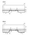
- FIG. 15A cross-sectional view of a section Y-Y in FIG.
- FIG. 15corresponds to FIG. 14 .
- FIG. 15shows only the semiconductor substrate 110 , the openings 110 A, the openings 117 , the bump electrodes 122 and the dicing lines DL out of the components shown in FIG. 14 , and the rest of the components are omitted for the sake of convenience of the explanation.
- the BGA type semiconductor deviceis described in Japanese Patent Application Publication No. 2005-72554, for example.
- the conventional semiconductor devicerequires an additional area of the semiconductor substrate 110 to form each of the semiconductor devices.
- the number of the semiconductor devices obtained from a wafer form of the semiconductor substrate 110has been reduced.
- the forming of the groove 123has made the manufacturing process of the semiconductor device more complicated to increase the manufacturing cost.
- the reliability of the semiconductor devicehas been reduced because the pad electrodes 112 are disposed outside a guard ring GR that protects internal components by surrounding them.
- the inventionprovides a semiconductor device that includes a semiconductor substrate having an opening formed therein, a supporter bonded to the top surface of the semiconductor substrate so as to cover the opening, an adhesive layer boding the supporter to the top surface of the semiconductor substrate, a plurality of pad electrodes disposed in the opening so as to be on the supporter, and a plurality of wiring layers electrically connected to corresponding pad electrodes in the opening.
- the supporter and the adhesive layermay be replaced with an insulation film.
- the inventionalso provides a method of manufacturing a semiconductor device.
- the methodincludes providing a semiconductor substrate, forming a plurality of pad electrodes in a predetermined region on a top surface of the semiconductor substrate, bonding a supporter to the top surface of the semiconductor substrate using an adhesive, forming an opening in the semiconductor substrate at the predetermined region so as to penetrate through the semiconductor substrate, forming a plurality of wiring layers on a bottom surface of the semiconductor substrate so that the wiring layers are electrically connected to corresponding pad electrodes in the opening, and dicing a stacked layer structure comprising the semiconductor substrate and the supporter along a dicing line to produce a semiconductor device so that the opening remains in the produced semiconductor device without being cut through.
- the inventionfurther provides a semiconductor device that includes a semiconductor substrate having a front surface and a back surface and having an opening penetrating through the semiconductor substrate, an insulating body disposed on the front surface of the semiconductor substrate and covering the opening of the semiconductor substrate, a plurality of pad electrodes disposed in the opening of the semiconductor substrate so as to be on the insulating body, and a plurality of wiring layers electrically connected to corresponding pad electrodes and disposed on the back surface of the semiconductor substrate.
- the wiring layersextend radially from the opening of the semiconductor substrate toward corresponding edges of the semiconductor substrate.
- FIG. 1is a cross-sectional view showing a semiconductor device and its manufacturing method according to an embodiment of this invention.
- FIG. 2is a plan view showing the semiconductor device according to the embodiment of this invention.
- FIG. 3is a cross-sectional view showing the semiconductor device and its manufacturing method according to the embodiment of this invention.
- FIG. 4is a cross-sectional view showing the semiconductor device and its manufacturing method according to the embodiment of this invention.
- FIG. 5is a cross-sectional view showing the semiconductor device and its manufacturing method according to the embodiment of this invention.
- FIG. 6is a cross-sectional view showing the semiconductor device and its manufacturing method according to the embodiment of this invention.
- FIG. 7is a cross-sectional view showing the semiconductor device and its manufacturing method according to the embodiment of this invention.
- FIG. 8is a plan view showing the semiconductor device and its manufacturing method according to the embodiment of this invention.
- FIG. 9is a plan view showing the semiconductor device according to the embodiment of this invention.
- FIG. 10is a plan view showing the semiconductor device according to the embodiment of this invention.
- FIG. 11is a plan view showing the semiconductor device according to the embodiment of this invention.
- FIG. 12is a plan view showing the semiconductor device according to the embodiment of this invention.
- FIG. 13is a plan view showing the semiconductor device according to the embodiment of this invention.
- FIG. 14is a cross-sectional view showing a conventional semiconductor device and its manufacturing method.
- FIG. 15is a cross-sectional view showing the conventional semiconductor device and its manufacturing method.
- FIG. 1is a cross-sectional view showing the semiconductor device and its manufacturing method.
- FIG. 1primarily shows one semiconductor device out of a plurality of the semiconductor devices formed in a wafer form of a semiconductor substrate 10 .
- the cross-sectional view shown in FIG. 1corresponds to a section X-X in an outline plan view shown in FIG. 2 .
- the pad electrodes 12may be made of aluminum and copper, or may be made of copper.
- the pad electrodes 12each connected with an electronic device (not shown) formed in the semiconductor substrate 10 , are electrically independent from each other and disposed together in a predetermined region away from dicing lines DL. In the device shown in FIGS. 1 and 2 , each pad electrode 12 connected to a respective electronic device is connected to bump electrode 22 for external connection formed on the back surface of the semiconductor substrate 10 .
- Four connections between the pad electrodes 12 and bump electrodes 22are made through an opening 10 A formed in the semiconductor substrate 10 .
- a horizontal shape of the semiconductor substrate 10is square or approximately square, for example.
- the pad electrodes 12are covered with an insulation film 13 made of a silicon nitride film or the like that makes a passivation film.
- a supporter 15is bonded to the top surface of the semiconductor substrate 10 through an adhesive layer 14 made of organic resin or the like.
- the supporter 15is made of glass in this embodiment. However, it may be made of other material such as resin or silicon.
- An opening 10 Ais formed in the semiconductor substrate 10 in a region overlapping the predetermined region where the plurality of pad electrodes 12 is disposed. That is, the plurality of pad electrodes 12 is disposed together in the opening 10 A.
- the opening 10 Ais thoroughly surrounded by the semiconductor substrate 10 , and is formed in a region not overlapping the dicing line DL.
- the opening 10 Ais horizontally shaped in a square with an edge that is 200 ⁇ m-500 ⁇ m long, for example. Further, it is preferable that the opening 10 A is formed at a location around or approximately around a center of the semiconductor device, in other words, at a location away from the dicing lines DL.
- An insulation film 16 made of a silicon oxide film or the likeis formed in the opening 10 A and extending over a back surface of the semiconductor substrate 10 .
- An opening 17is formed in the insulation films 11 and 16 in a region overlapping a portion of each of the pad electrodes 12 .
- the opening 17is horizontally shaped in a square with an edge that is 20 ⁇ m-80 ⁇ m long, for example.
- the wiring layer 18is formed to have a desired pattern.
- the wiring layer 18is made of aluminum, for example. However, it may be made of other material such as one including copper, for example, or may be made of copper.
- the wiring layer 18may be also used as a light-shielding film for the electronic device (not shown).
- the wiring layer 18is covered with an insulation film 19 made of a silicon oxide film or the like and a protection film 20 made of organic resin or the like.
- An opening that exposes a portion of the wiring layer 18is provided in the insulation film 19 and the protection film 20 that overlap the wiring layer 18 .
- a bump electrode 22 made of solder, gold or the likeis disposed on the plating layer 21 .
- the plating layer 21serves to connect the wiring layer 18 to the bump electrode 22 favorably.
- a distance between the pad electrode 12 and the dicing line DLis greater in the semiconductor device according to the embodiment of this invention than in the conventional semiconductor device, the corrosion of the pad electrode 12 due to the invasion of water or the like from the side surface of the semiconductor device occurs less likely, even when a cut surface is formed by a dicing blade (not shown) on the semiconductor substrate 10 at the dicing.
- the distance between the pad electrode 12 and the dicing line DLis greater in the semiconductor device according to the embodiment than in the conventional semiconductor device, there can be prevented a connection failure between the pad electrode 12 and the wiring layer 18 due to an impact caused when the dicing blade touches the semiconductor substrate 10 during the dicing.
- the semiconductor device according to the embodiment of this inventiondoes not require forming a groove similar to the groove 123 that extends partway through the thickness of the supporter 115 along the dicing line DL in the conventional semiconductor device in order to prevent the connection failure between the pad electrode 112 and the wiring layer 118 .
- an area of the semiconductor substrate 10 required to form the semiconductor device according to the embodimentis reduced by an amount of area required to form the groove 123 in the conventional semiconductor device, and the number of semiconductor devices obtained from a wafer form of the semiconductor substrate 10 is increased compared with the conventional semiconductor device.
- eliminating the need to form the groove as required in the conventional semiconductor devicemakes the manufacturing process simpler and reduces the manufacturing cost as a result.
- the semiconductor device according to the embodimentdoes not have a slanted plane on its side surface similar to a sidewall of the opening 110 A in the conventional semiconductor device, an area of the back surface can be increased compared with the conventional semiconductor device.
- mechanical strength of the semiconductor substrate 10is increased compared with that of the conventional semiconductor device, and mechanical strength of the semiconductor device at the time of assembly is also increased.
- the wiring layer 18is also used as the light-shielding film for the electronic device (not shown), a light-shielding capability can be increased as an area and flexibility in the patterning of the wiring layer 18 is increased compared with those of the conventional semiconductor device.
- the reliability of the semiconductor deviceis improved because the pad electrodes 12 are disposed inside the guard ring GR that is formed along a periphery of the semiconductor substrate 10 .
- FIG. 2shows only the semiconductor substrate 10 , the openings 10 A, the openings 17 , the bump electrodes 22 and the dicing lines DL out of the components shown in FIG. 1 and the rest of the components are omitted, for the sake of convenience of the explanation.
- FIGS. 3 through 7are cross-sectional views of the semiconductor device, and primarily show a region in which one semiconductor device out of a plurality of the semiconductor devices formed in the wafer form of the semiconductor substrate 10 is to be formed.
- a semiconductor substrate 10made of a silicon substrate of a thickness of approximately 100-700 ⁇ m, for example, as shown in FIG. 3 .
- Electronic devices(not shown), such as transistors, are formed in the top surface of the semiconductor substrate 10 .
- the electronic devicesare covered with the insulation film 11 made of the BPSG film or the like.
- the plurality of pad electrodes 12 that is electrically connected with the electronic devicesis formed on the insulation film 11 in the predetermined region away from the dicing lines DL.
- the predetermined regionis located around or approximately around a center of a region where the semiconductor device is to be formed. A case in which the predetermined region is located around the center of the region where the semiconductor device is to be formed is described hereafter.
- the passivation film 13 made of the silicon nitride film or the likeis formed to cover the pad electrodes 12 and the insulation film 11 .
- the adhesive layer 14is formed on the passivation film 13 by applying adhesive including organic resin or the like, and the supporter 15 is bonded to the top surface of the semiconductor substrate 10 through the adhesive layer 14 .
- the supporter 15is made of a material transparent to light or a material non-transparent to light, and is about 100-700 ⁇ m thick, for example.
- the supporter 15is made of glass, for example, in the explanation of the embodiment. However, it may be made of other material such as resin or silicon.
- the semiconductor substrate 10 in the region overlapping the predetermined region where the plurality of pad electrodes 12 is formedis removed by etching.
- the opening 10 Ais formed in the semiconductor substrate 10 in the region overlapping the predetermined region where the plurality of pad electrodes 12 is formed. That is, the plurality of pad electrodes 12 is in the opening 10 A.
- the opening 10 Ais formed in the region that does not overlap the dicing line DL.
- the insulation film 11is exposed in the bottom of the opening 10 A.
- a sidewall of the semiconductor substrate 10 in the opening 10 Ais formed to be tapered down toward the supporter 15 . By doing so, coverage of each of the layers formed to cover the semiconductor substrate 10 and the supporter 15 in subsequent process steps is improved.
- the insulation film 16 made of the silicon oxide film or the likeis formed to cover the inside of the opening 10 A and the back surface of the semiconductor substrate 10 .
- a portion of the insulation films 11 and 16 overlapping in the opening 10 Ais etched off to form the opening 17 that exposes a portion of each of the pad electrodes 12 , as shown in FIG. 5 .
- the wiring layer 18is formed that is connected with the pad electrode 12 through the opening 17 in the insulation films 11 and 16 and extending from the inside of the opening 10 A in the semiconductor substrate 10 to over the back surface of the semiconductor substrate 10 , as shown in FIG. 6 .
- the wiring layer 18is made of aluminum, for example. However, it may be made of other material such as one including copper, for example, or may be made of copper.
- the wiring layer 18is shaped into the desired pattern by etching using a mask (not shown) formed by photolithography or the like, as shown in FIG. 7 .
- the wiring layer 18does not overlap the dicing line DL, and an edge of the wiring layer 18 is located on an inner side (a side closer to the opening 10 A) than the dicing line DL in the example shown in the drawing.
- the insulation film 19 made of the silicon oxide film or the likeis formed to cover the wiring layer 18 .
- the opening to expose the portion of the wiring layer 18is formed in the insulation film 19 , and the plating layer 21 made of gold plating, for example, and connected with the wiring layer 18 is formed in the opening.
- the protection film 20 made of organic resin or the likeis formed to cover the insulation film 19 and the plating layer 21 .
- the opening to expose the plating layer 21is formed in the protection film 20 , and the bump electrode 22 made of solder, gold or the like is formed on the plating layer in the opening.
- the plating layer 21is horizontally shaped in a circle or in other shape such as a rectangle or a polygon, and the bump electrode 22 formed on it reflects the shape of the plating layer 21 and is also formed in the shape of the circle or in the other shape such as the rectangle or the polygon.
- the plating layer 21 and the bump electrode 22are depicted to be formed in the shape of the circle in the drawing.
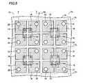
- FIG. 8Relative locations of openings 10 A in the semiconductor substrate 10 , the opening 17 in the insulation films 11 and 16 and the dicing lines DL described above are as shown in FIG. 8 when looked from the back surface-side of the semiconductor substrate 10 .
- a section X-X in FIG. 8corresponds to the cross-sectional views shown in FIGS. 3 through 7 .
- FIG. 8shows only the semiconductor substrate 10 , the openings 10 A, the openings 17 , the wiring layers 18 , the bump electrodes 22 and the dicing lines DL out of the components shown in FIGS. 3 through 7 , and the rest of the components are omitted for the sake of convenience of the explanation.
- the stacked layer structure including the semiconductor substrate 10 and the supporter 15are separated into a plurality of the semiconductor devices by dicing along the dicing lines DL. Since the pad electrodes 12 are located far away from the dicing lines DL, the corrosion of the pad electrodes 12 due to the invasion of water or the like from the side surface of the semiconductor device occurs less likely, even when the cut surface is formed by the dicing blade on the semiconductor substrate 10 and the supporter 15 at the dicing. Also, there can be prevented a connection failure between the pad electrode 12 and the wiring layer 18 due to the impact caused when the dicing blade touches the semiconductor substrate 10 .
- FIGS. 9 through 13are outline plan views of semiconductor devices according to the modified examples of the embodiment of this invention.
- Cross-sectional structures of the semiconductor devices according to the modified examplesare similar to the cross-sectional structure shown in FIG. 1 , and their manufacturing method is similar to the manufacturing method shown in FIGS. 3 through 7 . Thus, explanations on them are omitted.
- the pad electrode 12may be formed to have a shape of a rectangle as sown in FIG. 9 , for example.
- the openings 10 A and the openings 17may be formed in a circular shape as shown in FIG. 10 in order to minimize an area of the region in which the openings 10 A in the semiconductor substrate 10 and the openings 17 in the insulation films 11 and 16 are formed.
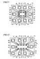
- each of the bump electrodes 22may be connected with corresponding each of the pad electrodes 12 in the opening 10 A in the semiconductor substrate 10 through corresponding each of the openings 17 in the insulation films 11 and 16 by a wiring layer 58 formed of the same material and by the same manufacturing method as the wiring layer 18 , as shown in FIG. 11 .
- some of the rectangle-shaped openings 17are disposed in the square-shaped opening 10 A along an edge of the opening 10 A in the semiconductor substrate 10 while some other openings 17 are disposed along an orthogonal edge.
- ten each of the openings 17 in the insulation films 11 and 16 and the bump electrodes 22may be disposed on the rectangle-shaped semiconductor substrate 10 as shown in FIG. 12 .
- the wiring layer 68 formed of the same material and by the same manufacturing method as the wiring layer 18preferably has a circular shape in the region where the bump electrode 22 is formed in order to increase flexibility in patterning the wiring layer.
- the plating layer 21is formed between the bump electrode 22 and the wiring layer 18 , 58 or 68 in the embodiment, the plating layer 21 is not necessarily formed and the bump electrode 22 may be directly connected with the wiring layer 18 , 58 or 68 .
- the wiring layer 18 , 58 or 68is made of copper, for example, the material gives a good electrical connection by its nature even when the bump electrode 22 is directly connected with the wiring layer 18 , 58 or 68 .
- the bump electrodes 22are not necessarily formed in the embodiment described above.
- conductive paste(not shown) including silver or the like may be formed instead of the bump electrode 22 .
- an opening to expose the pad electrode 12may be formed in the supporter 15 and a wiring layer or an electrode connected with the pad electrode 12 through the opening may be formed in the embodiment described above.
- another of the semiconductor devicecan be stacked on top of the supporter 15 so that two of the semiconductor devices are electrically connected through the wiring layer or the electrode described above.
- the supporter 15may be removed after dicing the stacked layer structure including the semiconductor substrate 10 and the supporter 15 in the embodiment described above. That is, the embodiment may be applied to the semiconductor device that does not include the supporter 15 in the finished product.
- the insulation film 13may be formed thick enough to have a sufficient mechanical strength to replace the supporter 15 .
- a protection filmmay be formed over the insulation film 13 .
- a material of the protection filmis not specified, and may be made of organic resin, for example.
- an opening to expose the pad electrode 12may be formed in the insulation film 13 or in the insulation film 13 and the protection film thereon, and a wiring layer or an electrode connected with the pad electrode 12 through the opening may be formed on the insulation film 13 or on the protection film.
- another of the semiconductor devicecan be stacked on top of the insulation film 13 or on top of the protection film so that two of the semiconductor devices are electrically connected through the wiring layer or the electrode described above.
- forming the groove along the dicing line as required in the conventional artis no longer necessary, since the pad electrodes are not disposed in the periphery of the semiconductor device, i.e. in the vicinity of the dicing line.
- the area of the semiconductor substrate required to form the semiconductor deviceis reduced compared with the conventional art, and the number of the semiconductor devices obtained from a wafer form of the semiconductor substrate is increased.
- eliminating the need to form the groovemakes the manufacturing process simpler and reduces the manufacturing cost as a result.
- the reliability of the semiconductor deviceis improved because the pad electrodes are disposed inside the guard ring.
Landscapes
- Engineering & Computer Science (AREA)
- Computer Hardware Design (AREA)
- Microelectronics & Electronic Packaging (AREA)
- Power Engineering (AREA)
- Physics & Mathematics (AREA)
- Condensed Matter Physics & Semiconductors (AREA)
- General Physics & Mathematics (AREA)
- Manufacturing & Machinery (AREA)
- Internal Circuitry In Semiconductor Integrated Circuit Devices (AREA)
Abstract
Description
- This application claims priority from Japanese Patent Application No. 2008-273229, the content of which is incorporated herein by reference in its entirety.
- 1. Field of the Invention
- This invention relates to a semiconductor device and its manufacturing method, specifically to a chip size package and its manufacturing method.
- 2. Description of the Related Art
- A CSP (Chip Size Package) has received attention in recent years as a new packaging technology. The CSP means a small package having about the same outside dimensions as those of a semiconductor die packaged in it.
- A BGA (Ball Grid Array) type semiconductor device is known as a kind of chip size package device. An example structure of the BGA type semiconductor device is described hereafter.
- A
pad electrode 112 is disposed on aninsulation film 111 disposed on a top surface of asemiconductor substrate 110 that constitutes the semiconductor device, as shown in a cross-sectional view ofFIG. 14 . Thepad electrode 112 is connected with an electronic device (not shown) formed in thesemiconductor substrate 110. Thepad electrode 112 is covered with aninsulation film 113 that makes a passivation film. Asupporter 115 is bonded to the top surface of thesemiconductor substrate 110 through anadhesive layer 114. - On the other hand, an opening110A is formed from a back surface of the
semiconductor substrate 110 in a region overlapping thepad electrode 112 and a dicing line DL. Aninsulation film 116 is formed in an inside of the opening110A and over the back surface of thesemiconductor substrate 110. Anopening 117 that exposes a portion of thepad electrode 112 is formed in theinsulation films pad electrode 112. On theinsulation film 116, there is disposed awiring layer 118 that is connected with thepad electrode 112 through theopening 117. Thewiring layer 118 is covered with aninsulation film 119 and aprotection film 120. An opening that exposes a portion of thewiring layer 118 is provided in theinsulation film 119 and theprotection film 120 that overlap thewiring layer 118. Aplating layer 121 made of gold plating, for example, is disposed on thewiring layer 118 in the opening. Abump electrode 122 is disposed on theplating layer 121. - A
groove 123 extending partway through a thickness of thesupporter 115 is formed along the dicing line DL in the opening110A in the semiconductor substrate. Theprotection film 120 covers thegroove 123. The structure as described above eliminates a possibility that a damaged layer which allows invasion of water or the like to corrode thepad electrode 112 in the semiconductor device after dicing is caused on a side surface of thesemiconductor substrate 110. Also, there can be prevented a connection failure between thepad electrode 112 and thewiring layer 118 due to an impact caused when a dicing blade touches thesemiconductor substrate 110. - The structure described above looks as shown in
FIG. 15 when looked from a back surface-side of thesemiconductor substrate 110. A cross-sectional view of a section Y-Y in FIG. - 15 corresponds to
FIG. 14 .FIG. 15 shows only thesemiconductor substrate 110, theopenings 110A, theopenings 117, thebump electrodes 122 and the dicing lines DL out of the components shown inFIG. 14 , and the rest of the components are omitted for the sake of convenience of the explanation. - The BGA type semiconductor device is described in Japanese Patent Application Publication No. 2005-72554, for example.
- As described above, there is a need to secure a region corresponding to a width of the
groove 123 between a pair of thepad electrodes 112 astride the dicing line DL in order to prevent the corrosion of thepad electrode 112 and the connection failure between thepad electrode 112 and thewiring layer 118, when thegroove 123 is formed along the dicing line DL and covered with theprotection film 120. That is, the conventional semiconductor device requires an additional area of thesemiconductor substrate 110 to form each of the semiconductor devices. As a result, the number of the semiconductor devices obtained from a wafer form of thesemiconductor substrate 110 has been reduced. In addition, the forming of thegroove 123 has made the manufacturing process of the semiconductor device more complicated to increase the manufacturing cost. Furthermore, the reliability of the semiconductor device has been reduced because thepad electrodes 112 are disposed outside a guard ring GR that protects internal components by surrounding them. - The invention provides a semiconductor device that includes a semiconductor substrate having an opening formed therein, a supporter bonded to the top surface of the semiconductor substrate so as to cover the opening, an adhesive layer boding the supporter to the top surface of the semiconductor substrate, a plurality of pad electrodes disposed in the opening so as to be on the supporter, and a plurality of wiring layers electrically connected to corresponding pad electrodes in the opening. The supporter and the adhesive layer may be replaced with an insulation film.
- The invention also provides a method of manufacturing a semiconductor device. The method includes providing a semiconductor substrate, forming a plurality of pad electrodes in a predetermined region on a top surface of the semiconductor substrate, bonding a supporter to the top surface of the semiconductor substrate using an adhesive, forming an opening in the semiconductor substrate at the predetermined region so as to penetrate through the semiconductor substrate, forming a plurality of wiring layers on a bottom surface of the semiconductor substrate so that the wiring layers are electrically connected to corresponding pad electrodes in the opening, and dicing a stacked layer structure comprising the semiconductor substrate and the supporter along a dicing line to produce a semiconductor device so that the opening remains in the produced semiconductor device without being cut through.
- The invention further provides a semiconductor device that includes a semiconductor substrate having a front surface and a back surface and having an opening penetrating through the semiconductor substrate, an insulating body disposed on the front surface of the semiconductor substrate and covering the opening of the semiconductor substrate, a plurality of pad electrodes disposed in the opening of the semiconductor substrate so as to be on the insulating body, and a plurality of wiring layers electrically connected to corresponding pad electrodes and disposed on the back surface of the semiconductor substrate. In plan view of the semiconductor device, the wiring layers extend radially from the opening of the semiconductor substrate toward corresponding edges of the semiconductor substrate.
FIG. 1 is a cross-sectional view showing a semiconductor device and its manufacturing method according to an embodiment of this invention.FIG. 2 is a plan view showing the semiconductor device according to the embodiment of this invention.FIG. 3 is a cross-sectional view showing the semiconductor device and its manufacturing method according to the embodiment of this invention.FIG. 4 is a cross-sectional view showing the semiconductor device and its manufacturing method according to the embodiment of this invention.FIG. 5 is a cross-sectional view showing the semiconductor device and its manufacturing method according to the embodiment of this invention.FIG. 6 is a cross-sectional view showing the semiconductor device and its manufacturing method according to the embodiment of this invention.FIG. 7 is a cross-sectional view showing the semiconductor device and its manufacturing method according to the embodiment of this invention.FIG. 8 is a plan view showing the semiconductor device and its manufacturing method according to the embodiment of this invention.FIG. 9 is a plan view showing the semiconductor device according to the embodiment of this invention.FIG. 10 is a plan view showing the semiconductor device according to the embodiment of this invention.FIG. 11 is a plan view showing the semiconductor device according to the embodiment of this invention.FIG. 12 is a plan view showing the semiconductor device according to the embodiment of this invention.FIG. 13 is a plan view showing the semiconductor device according to the embodiment of this invention.FIG. 14 is a cross-sectional view showing a conventional semiconductor device and its manufacturing method.FIG. 15 is a cross-sectional view showing the conventional semiconductor device and its manufacturing method.- A semiconductor device according to an embodiment of this invention is hereafter described referring to the drawings. First, a structure of the semiconductor device will be described.
FIG. 1 is a cross-sectional view showing the semiconductor device and its manufacturing method.FIG. 1 primarily shows one semiconductor device out of a plurality of the semiconductor devices formed in a wafer form of asemiconductor substrate 10. The cross-sectional view shown inFIG. 1 corresponds to a section X-X in an outline plan view shown inFIG. 2 . - An
insulation film 11 made of a BPSG (Boro-Phospho Silicate Glass) film or the like is disposed on a top surface of thesemiconductor substrate 10 constituting the semiconductor device, and a plurality ofpad electrodes 12 made of aluminum or the like is disposed on it, as shown inFIG. 1 . Thepad electrodes 12 may be made of aluminum and copper, or may be made of copper. Thepad electrodes 12, each connected with an electronic device (not shown) formed in thesemiconductor substrate 10, are electrically independent from each other and disposed together in a predetermined region away from dicing lines DL. In the device shown inFIGS. 1 and 2 , eachpad electrode 12 connected to a respective electronic device is connected to bumpelectrode 22 for external connection formed on the back surface of thesemiconductor substrate 10. Four connections between thepad electrodes 12 and bumpelectrodes 22 are made through anopening 10A formed in thesemiconductor substrate 10. - A horizontal shape of the
semiconductor substrate 10 is square or approximately square, for example. - The
pad electrodes 12 are covered with aninsulation film 13 made of a silicon nitride film or the like that makes a passivation film. Asupporter 15 is bonded to the top surface of thesemiconductor substrate 10 through anadhesive layer 14 made of organic resin or the like. Thesupporter 15 is made of glass in this embodiment. However, it may be made of other material such as resin or silicon. - An
opening 10A is formed in thesemiconductor substrate 10 in a region overlapping the predetermined region where the plurality ofpad electrodes 12 is disposed. That is, the plurality ofpad electrodes 12 is disposed together in theopening 10A. Theopening 10A is thoroughly surrounded by thesemiconductor substrate 10, and is formed in a region not overlapping the dicing line DL. Theopening 10A is horizontally shaped in a square with an edge that is 200 μm-500 μm long, for example. Further, it is preferable that theopening 10A is formed at a location around or approximately around a center of the semiconductor device, in other words, at a location away from the dicing lines DL. Aninsulation film 16 made of a silicon oxide film or the like is formed in theopening 10A and extending over a back surface of thesemiconductor substrate 10. - An
opening 17 is formed in theinsulation films pad electrodes 12. Theopening 17 is horizontally shaped in a square with an edge that is 20 μm-80 μm long, for example. - There is disposed a
wiring layer 18 that is connected with each of thepad electrodes 12 through corresponding each of theopenings 17. Thewiring layer 18 is formed to have a desired pattern. Thewiring layer 18 is made of aluminum, for example. However, it may be made of other material such as one including copper, for example, or may be made of copper. Thewiring layer 18 may be also used as a light-shielding film for the electronic device (not shown). Thewiring layer 18 is covered with aninsulation film 19 made of a silicon oxide film or the like and aprotection film 20 made of organic resin or the like. - An opening that exposes a portion of the
wiring layer 18 is provided in theinsulation film 19 and theprotection film 20 that overlap thewiring layer 18. Aplating layer 21 made of gold plating, for example, is disposed on thewiring layer 18 in the opening. Abump electrode 22 made of solder, gold or the like is disposed on theplating layer 21. Theplating layer 21 serves to connect thewiring layer 18 to thebump electrode 22 favorably. - Since a distance between the
pad electrode 12 and the dicing line DL is greater in the semiconductor device according to the embodiment of this invention than in the conventional semiconductor device, the corrosion of thepad electrode 12 due to the invasion of water or the like from the side surface of the semiconductor device occurs less likely, even when a cut surface is formed by a dicing blade (not shown) on thesemiconductor substrate 10 at the dicing. - Also because the distance between the
pad electrode 12 and the dicing line DL is greater in the semiconductor device according to the embodiment than in the conventional semiconductor device, there can be prevented a connection failure between thepad electrode 12 and thewiring layer 18 due to an impact caused when the dicing blade touches thesemiconductor substrate 10 during the dicing. - That is, the semiconductor device according to the embodiment of this invention does not require forming a groove similar to the
groove 123 that extends partway through the thickness of thesupporter 115 along the dicing line DL in the conventional semiconductor device in order to prevent the connection failure between thepad electrode 112 and thewiring layer 118. - Thus, an area of the
semiconductor substrate 10 required to form the semiconductor device according to the embodiment is reduced by an amount of area required to form thegroove 123 in the conventional semiconductor device, and the number of semiconductor devices obtained from a wafer form of thesemiconductor substrate 10 is increased compared with the conventional semiconductor device. In addition, eliminating the need to form the groove as required in the conventional semiconductor device makes the manufacturing process simpler and reduces the manufacturing cost as a result. - Since the semiconductor device according to the embodiment does not have a slanted plane on its side surface similar to a sidewall of the
opening 110A in the conventional semiconductor device, an area of the back surface can be increased compared with the conventional semiconductor device. As a result, mechanical strength of thesemiconductor substrate 10 is increased compared with that of the conventional semiconductor device, and mechanical strength of the semiconductor device at the time of assembly is also increased. When thewiring layer 18 is also used as the light-shielding film for the electronic device (not shown), a light-shielding capability can be increased as an area and flexibility in the patterning of thewiring layer 18 is increased compared with those of the conventional semiconductor device. - In addition, the reliability of the semiconductor device is improved because the
pad electrodes 12 are disposed inside the guard ring GR that is formed along a periphery of thesemiconductor substrate 10. - The structure described above looks as shown in
FIG. 2 , when looked from a back surface-side of thesemiconductor substrate 10. The cross-sectional view of the section X-X inFIG. 2 corresponds toFIG. 1 .FIG. 2 shows only thesemiconductor substrate 10, theopenings 10A, theopenings 17, thebump electrodes 22 and the dicing lines DL out of the components shown inFIG. 1 and the rest of the components are omitted, for the sake of convenience of the explanation. - Next, a method of manufacturing the semiconductor device having the structure as described above will be explained referring to the drawings.
FIGS. 3 through 7 are cross-sectional views of the semiconductor device, and primarily show a region in which one semiconductor device out of a plurality of the semiconductor devices formed in the wafer form of thesemiconductor substrate 10 is to be formed. - First, there is provided a
semiconductor substrate 10 made of a silicon substrate of a thickness of approximately 100-700 μm, for example, as shown inFIG. 3 . Electronic devices (not shown), such as transistors, are formed in the top surface of thesemiconductor substrate 10. The electronic devices are covered with theinsulation film 11 made of the BPSG film or the like. - Next, the plurality of
pad electrodes 12 that is electrically connected with the electronic devices is formed on theinsulation film 11 in the predetermined region away from the dicing lines DL. - It is preferable that the predetermined region is located around or approximately around a center of a region where the semiconductor device is to be formed. A case in which the predetermined region is located around the center of the region where the semiconductor device is to be formed is described hereafter.
- Next, the
passivation film 13 made of the silicon nitride film or the like is formed to cover thepad electrodes 12 and theinsulation film 11. After that, theadhesive layer 14 is formed on thepassivation film 13 by applying adhesive including organic resin or the like, and thesupporter 15 is bonded to the top surface of thesemiconductor substrate 10 through theadhesive layer 14. Thesupporter 15 is made of a material transparent to light or a material non-transparent to light, and is about 100-700 μm thick, for example. Thesupporter 15 is made of glass, for example, in the explanation of the embodiment. However, it may be made of other material such as resin or silicon. - Next, back-grinding is performed on the
semiconductor substrate 10 bonded to thesupporter 15 until the thickness of thesemiconductor substrate 10 is reduced to 50-150 μm, for example, as shown inFIG. 4 . - The
semiconductor substrate 10 in the region overlapping the predetermined region where the plurality ofpad electrodes 12 is formed is removed by etching. As a result, theopening 10A is formed in thesemiconductor substrate 10 in the region overlapping the predetermined region where the plurality ofpad electrodes 12 is formed. That is, the plurality ofpad electrodes 12 is in theopening 10A. Theopening 10A is formed in the region that does not overlap the dicing line DL. Theinsulation film 11 is exposed in the bottom of theopening 10A. - It is preferable that a sidewall of the
semiconductor substrate 10 in theopening 10A is formed to be tapered down toward thesupporter 15. By doing so, coverage of each of the layers formed to cover thesemiconductor substrate 10 and thesupporter 15 in subsequent process steps is improved. - Next, the
insulation film 16 made of the silicon oxide film or the like is formed to cover the inside of theopening 10A and the back surface of thesemiconductor substrate 10. - After that, a portion of the
insulation films opening 10A is etched off to form theopening 17 that exposes a portion of each of thepad electrodes 12, as shown inFIG. 5 . - Next, there is formed the
wiring layer 18 that is connected with thepad electrode 12 through theopening 17 in theinsulation films opening 10A in thesemiconductor substrate 10 to over the back surface of thesemiconductor substrate 10, as shown inFIG. 6 . Thewiring layer 18 is made of aluminum, for example. However, it may be made of other material such as one including copper, for example, or may be made of copper. - Next, the
wiring layer 18 is shaped into the desired pattern by etching using a mask (not shown) formed by photolithography or the like, as shown inFIG. 7 . Thewiring layer 18 does not overlap the dicing line DL, and an edge of thewiring layer 18 is located on an inner side (a side closer to theopening 10A) than the dicing line DL in the example shown in the drawing. - After that, the
insulation film 19 made of the silicon oxide film or the like is formed to cover thewiring layer 18. The opening to expose the portion of thewiring layer 18 is formed in theinsulation film 19, and theplating layer 21 made of gold plating, for example, and connected with thewiring layer 18 is formed in the opening. Furthermore, theprotection film 20 made of organic resin or the like is formed to cover theinsulation film 19 and theplating layer 21. The opening to expose theplating layer 21 is formed in theprotection film 20, and thebump electrode 22 made of solder, gold or the like is formed on the plating layer in the opening. Theplating layer 21 is horizontally shaped in a circle or in other shape such as a rectangle or a polygon, and thebump electrode 22 formed on it reflects the shape of theplating layer 21 and is also formed in the shape of the circle or in the other shape such as the rectangle or the polygon. Theplating layer 21 and thebump electrode 22 are depicted to be formed in the shape of the circle in the drawing. - Relative locations of
openings 10A in thesemiconductor substrate 10, theopening 17 in theinsulation films FIG. 8 when looked from the back surface-side of thesemiconductor substrate 10. A section X-X inFIG. 8 corresponds to the cross-sectional views shown inFIGS. 3 through 7 .FIG. 8 shows only thesemiconductor substrate 10, theopenings 10A, theopenings 17, the wiring layers18, thebump electrodes 22 and the dicing lines DL out of the components shown inFIGS. 3 through 7 , and the rest of the components are omitted for the sake of convenience of the explanation. - After that, the stacked layer structure including the
semiconductor substrate 10 and thesupporter 15 are separated into a plurality of the semiconductor devices by dicing along the dicing lines DL. Since thepad electrodes 12 are located far away from the dicing lines DL, the corrosion of thepad electrodes 12 due to the invasion of water or the like from the side surface of the semiconductor device occurs less likely, even when the cut surface is formed by the dicing blade on thesemiconductor substrate 10 and thesupporter 15 at the dicing. Also, there can be prevented a connection failure between thepad electrode 12 and thewiring layer 18 due to the impact caused when the dicing blade touches thesemiconductor substrate 10. - The relative locations of the
openings 17 in theinsulation films bump electrodes 22 are not limited to those shown inFIG. 2 andFIG. 8 , and may be those in modified examples as described below.FIGS. 9 through 13 are outline plan views of semiconductor devices according to the modified examples of the embodiment of this invention. Cross-sectional structures of the semiconductor devices according to the modified examples are similar to the cross-sectional structure shown inFIG. 1 , and their manufacturing method is similar to the manufacturing method shown inFIGS. 3 through 7 . Thus, explanations on them are omitted. - The
pad electrode 12 may be formed to have a shape of a rectangle as sown inFIG. 9 , for example. - Also, the
openings 10A and theopenings 17 may be formed in a circular shape as shown inFIG. 10 in order to minimize an area of the region in which theopenings 10A in thesemiconductor substrate 10 and theopenings 17 in theinsulation films - Also, when ten each of the
openings 17 in theinsulation films bump electrodes 22 are disposed on the square-shapedsemiconductor substrate 10, each of thebump electrodes 22 may be connected with corresponding each of thepad electrodes 12 in theopening 10A in thesemiconductor substrate 10 through corresponding each of theopenings 17 in theinsulation films wiring layer 58 formed of the same material and by the same manufacturing method as thewiring layer 18, as shown inFIG. 11 . In this example, some of the rectangle-shapedopenings 17 are disposed in the square-shapedopening 10A along an edge of theopening 10A in thesemiconductor substrate 10 while someother openings 17 are disposed along an orthogonal edge. - Or, ten each of the
openings 17 in theinsulation films bump electrodes 22 may be disposed on the rectangle-shapedsemiconductor substrate 10 as shown inFIG. 12 . - Or, twelve each of the
openings 17 in theinsulation films bump electrodes 22 may be disposed on the rectangle-shapedsemiconductor substrate 10 as shown inFIG. 13 . In this case, thewiring layer 68 formed of the same material and by the same manufacturing method as thewiring layer 18 preferably has a circular shape in the region where thebump electrode 22 is formed in order to increase flexibility in patterning the wiring layer. - It is apparent that this invention is not limited to the embodiment described above and may be modified within the scope of the invention.
- For example, although the
plating layer 21 is formed between thebump electrode 22 and thewiring layer plating layer 21 is not necessarily formed and thebump electrode 22 may be directly connected with thewiring layer wiring layer bump electrode 22 is directly connected with thewiring layer - Also, the
bump electrodes 22 are not necessarily formed in the embodiment described above. For example, conductive paste (not shown) including silver or the like may be formed instead of thebump electrode 22. - Also, an opening to expose the
pad electrode 12 may be formed in thesupporter 15 and a wiring layer or an electrode connected with thepad electrode 12 through the opening may be formed in the embodiment described above. With this structure, another of the semiconductor device can be stacked on top of thesupporter 15 so that two of the semiconductor devices are electrically connected through the wiring layer or the electrode described above. - Also, the
supporter 15 may be removed after dicing the stacked layer structure including thesemiconductor substrate 10 and thesupporter 15 in the embodiment described above. That is, the embodiment may be applied to the semiconductor device that does not include thesupporter 15 in the finished product. In this case, theinsulation film 13 may be formed thick enough to have a sufficient mechanical strength to replace thesupporter 15. In addition, a protection film may be formed over theinsulation film 13. A material of the protection film is not specified, and may be made of organic resin, for example. - In addition, an opening to expose the
pad electrode 12 may be formed in theinsulation film 13 or in theinsulation film 13 and the protection film thereon, and a wiring layer or an electrode connected with thepad electrode 12 through the opening may be formed on theinsulation film 13 or on the protection film. With this structure, another of the semiconductor device can be stacked on top of theinsulation film 13 or on top of the protection film so that two of the semiconductor devices are electrically connected through the wiring layer or the electrode described above. - According to the embodiment of this invention, forming the groove along the dicing line as required in the conventional art is no longer necessary, since the pad electrodes are not disposed in the periphery of the semiconductor device, i.e. in the vicinity of the dicing line. As a result, the area of the semiconductor substrate required to form the semiconductor device is reduced compared with the conventional art, and the number of the semiconductor devices obtained from a wafer form of the semiconductor substrate is increased. In addition, eliminating the need to form the groove makes the manufacturing process simpler and reduces the manufacturing cost as a result. Furthermore, the reliability of the semiconductor device is improved because the pad electrodes are disposed inside the guard ring.
Claims (9)
Applications Claiming Priority (2)
| Application Number | Priority Date | Filing Date | Title |
|---|---|---|---|
| JP2008273229AJP2010103300A (en) | 2008-10-23 | 2008-10-23 | Semiconductor device, and method of manufacturing the same |
| JP2008-273229 | 2008-10-23 |
Publications (2)
| Publication Number | Publication Date |
|---|---|
| US20100102460A1true US20100102460A1 (en) | 2010-04-29 |
| US8598720B2 US8598720B2 (en) | 2013-12-03 |
Family
ID=42116687
Family Applications (1)
| Application Number | Title | Priority Date | Filing Date |
|---|---|---|---|
| US12/575,687Active2030-02-20US8598720B2 (en) | 2008-10-23 | 2009-10-08 | Semiconductor device and manufacturing method thereof |
Country Status (3)
| Country | Link |
|---|---|
| US (1) | US8598720B2 (en) |
| JP (1) | JP2010103300A (en) |
| CN (1) | CN101728348B (en) |
Cited By (5)
| Publication number | Priority date | Publication date | Assignee | Title |
|---|---|---|---|---|
| US20120018849A1 (en)* | 2010-07-20 | 2012-01-26 | On Semiconductor Trading, Ltd. | Semiconductor device and method of manufacturing the same |
| US20120032307A1 (en)* | 2010-08-06 | 2012-02-09 | On Semiconductor Trading, Ltd. | Semiconductor device and method of manufacturing the same |
| US9331256B2 (en) | 2013-08-21 | 2016-05-03 | Xintec Inc. | Semiconductor structure with sensor chip and landing pads |
| US20160322312A1 (en)* | 2015-05-01 | 2016-11-03 | Xintec Inc. | Chip package and manufacturing method thereof |
| US20210272920A1 (en)* | 2018-02-23 | 2021-09-02 | Semiconductor Components Industries, Llc | Semiconductor device with backmetal and related methods |
Families Citing this family (5)
| Publication number | Priority date | Publication date | Assignee | Title |
|---|---|---|---|---|
| TWI525673B (en)* | 2013-10-08 | 2016-03-11 | 精材科技股份有限公司 | Method of fabricating a wafer-level chip package |
| WO2016117124A1 (en)* | 2015-01-23 | 2016-07-28 | オリンパス株式会社 | Image-capturing device and endoscope |
| JP2017010962A (en)* | 2015-06-16 | 2017-01-12 | 株式会社東芝 | Device substrate and method of manufacturing device substrate, and method of manufacturing semiconductor device |
| CN105552054B (en)* | 2016-02-03 | 2018-02-27 | 美新半导体(无锡)有限公司 | A kind of wafer level packaging structure and its manufacture method |
| JP2019160893A (en)* | 2018-03-09 | 2019-09-19 | ソニーセミコンダクタソリューションズ株式会社 | Solid state imaging element, semiconductor device, electronic device, and manufacturing method |
Citations (48)
| Publication number | Priority date | Publication date | Assignee | Title |
|---|---|---|---|---|
| US5122856A (en)* | 1987-11-13 | 1992-06-16 | Nissan Motor Co., Ltd. | Semiconductor device |
| US5606198A (en)* | 1993-10-13 | 1997-02-25 | Yamaha Corporation | Semiconductor chip with electrodes on side surface |
| US5923995A (en)* | 1997-04-18 | 1999-07-13 | National Semiconductor Corporation | Methods and apparatuses for singulation of microelectromechanical systems |
| US6153448A (en)* | 1997-05-14 | 2000-11-28 | Kabushiki Kaisha Toshiba | Semiconductor device manufacturing method |
| US20020013061A1 (en)* | 1996-10-29 | 2002-01-31 | Oleg Siniaguine | Thinning and dicing of semiconductor wafers using dry etch, and obtaining semiconductor chips with rounded bottom edges and corners |
| US20020016024A1 (en)* | 1999-07-26 | 2002-02-07 | Thomas Danielle A. | Backside contact for touchchip |
| US20020055265A1 (en)* | 2000-04-11 | 2002-05-09 | Zoltan Ring | Method of forming vias in silicon carbide and resulting devices and circuits |
| US6656758B1 (en)* | 1999-10-13 | 2003-12-02 | Sanyo Electric Co., Ltd. | Method of manufacturing a chip size package |
| US20030230805A1 (en)* | 2002-04-23 | 2003-12-18 | Sanyo Electric Co., Ltd. | Semiconductor device and manufacturing method thereof |
| US20040087130A1 (en)* | 2000-09-19 | 2004-05-06 | Atsushi Kazama | Semiconductor device and mounted semiconductor device structure |
| US20040115902A1 (en)* | 2002-10-15 | 2004-06-17 | Seiko Epson Corporation | Semiconductor device, method of manufacturing the same, circuit board, and electronic equipment |
| US20040137701A1 (en)* | 2002-10-11 | 2004-07-15 | Sanyo Electric Co., Ltd. | Semiconductor device and manufacturing method thereof |
| US20040137723A1 (en)* | 2002-10-30 | 2004-07-15 | Sanyo Electric Co., Ltd. | Manufacturing method of semiconductor device |
| US20040161920A1 (en)* | 2002-12-13 | 2004-08-19 | Sanyo Electric Co., Ltd. | Semiconductor device manufacturing method |
| US6781244B2 (en)* | 2002-05-13 | 2004-08-24 | National Semiconductor Corporation | Electrical die contact structure and fabrication method |
| US20050003649A1 (en)* | 2003-06-09 | 2005-01-06 | Sanyo Electric Co., Ltd. | Semiconductor device and manufacturing method thereof |
| US20050009238A1 (en)* | 2003-02-06 | 2005-01-13 | Mitsuru Okigawa | Semiconductor integrated device including support substrate fastened using resin, and manufacturing method thereof |
| US20050176235A1 (en)* | 2002-06-18 | 2005-08-11 | Sanyo Electric Co., Ltd. | Manufacturing method of semiconductor device |
| US20050194670A1 (en)* | 2004-02-17 | 2005-09-08 | Sanyo Electric Co., Ltd. | Semiconductor device and manufacturing method of the same |
| US20050208735A1 (en)* | 2004-03-05 | 2005-09-22 | Sanyo Electric Co., Ltd. | Semiconductor device and manufacturing method of the same |
| US20050269696A1 (en)* | 2004-05-24 | 2005-12-08 | Sanyo Electric Co., Ltd. | Semiconductor device and manufacturing method of the same |
| US20050269698A1 (en)* | 2004-06-02 | 2005-12-08 | Casio Computer Co., Ltd. | Semiconductor device having adhesion increasing film and method of fabricating the same |
| US20060024949A1 (en)* | 2004-07-29 | 2006-02-02 | Sanyo Electric Co., Ltd. | Method of manufacturing semiconductor device |
| US20060068572A1 (en)* | 2004-09-24 | 2006-03-30 | Sanyo Electric Co., Ltd. | Semiconductor device manufacturing method |
| US20060079025A1 (en)* | 2004-10-12 | 2006-04-13 | Agency For Science, Technology And Research | Polymer encapsulated dicing lane (PEDL) technology for Cu/low/ultra-low k devices |
| US7102238B2 (en)* | 2003-04-24 | 2006-09-05 | Sanyo Electric Co., Ltd. | Semiconductor device and manufacturing method thereof |
| US7241679B2 (en)* | 2004-02-17 | 2007-07-10 | Sanyo Electric Co., Ltd. | Method of manufacturing semiconductor device |
| US20070166957A1 (en)* | 2005-12-28 | 2007-07-19 | Sanyo Electric Co., Ltd | Method of manufacturing semiconductor device |
| US20070210437A1 (en)* | 2006-03-07 | 2007-09-13 | Sanyo Electric Co., Ltd. | Semiconductor device and manufacturing method thereof |
| US7374972B2 (en)* | 2005-07-15 | 2008-05-20 | Samsung Electronics Co., Ltd. | Micro-package, multi-stack micro-package, and manufacturing method therefor |
| US20080135967A1 (en)* | 2006-11-20 | 2008-06-12 | Sanyo Electric Co., Ltd. | Semiconductor device and method of manufacturing the same |
| US7397134B2 (en)* | 2004-06-10 | 2008-07-08 | Sanyo Electric Co., Ltd. | Semiconductor device mounted on and electrically connected to circuit board |
| US20080171421A1 (en)* | 2003-02-25 | 2008-07-17 | Sanyo Electric Co., Ltd. | Manufacturing method of semiconductor device with smoothing |
| US20080203557A1 (en)* | 2007-01-30 | 2008-08-28 | Sanyo Electric Co., Ltd. | Semiconductor module and method of manufacturing the same |
| US20080217743A1 (en)* | 2007-03-06 | 2008-09-11 | Olympus Corporation | Method of manufacturing semiconductor device and semiconductor device |
| US7435621B2 (en)* | 2005-05-03 | 2008-10-14 | Advanced Semiconductor Engineering, Inc. | Method of fabricating wafer level package |
| US20080277793A1 (en)* | 2007-05-07 | 2008-11-13 | Sanyo Electric Co., Ltd. | Semiconductor Device and Manufacturing Method Thereof |
| US20090015285A1 (en)* | 2007-07-11 | 2009-01-15 | International Business Machines Corporation | Test structures for electrically detecting back end of the line failures and methods of making and using the same |
| US20090026610A1 (en)* | 2007-07-27 | 2009-01-29 | Sanyo Electric Co., Ltd. | Semiconductor device and method of manufacturing the same |
| US20090095974A1 (en)* | 2007-10-11 | 2009-04-16 | Shinko Electric Industries Co., Ltd. | Semiconductor package and manufacturing method thereof |
| US20100038668A1 (en)* | 2007-02-02 | 2010-02-18 | Sanyo Semiconductor Co., Ltd. | Semiconductor device and method of manufacturing the same |
| US20100038742A1 (en)* | 2006-09-11 | 2010-02-18 | Sanyo Electric Co., Ltd. | Semiconductor device and manufacturing method thereof |
| US7728445B2 (en)* | 2005-03-16 | 2010-06-01 | Yamaha Corporation | Semiconductor device production method and semiconductor device |
| US7790506B2 (en)* | 2006-12-13 | 2010-09-07 | Yamaha Corporation | Method of manufacturing semiconductor devices encapsulated in chip size packages |
| US7897509B2 (en)* | 2006-09-28 | 2011-03-01 | Renesas Electronics Corp. | Semiconductor wafer and method of manufacturing the same and method of manufacturing semiconductor device |
| US7919875B2 (en)* | 2003-08-06 | 2011-04-05 | Sanyo Electric Co., Ltd. | Semiconductor device with recess portion over pad electrode |
| US7986021B2 (en)* | 2005-12-15 | 2011-07-26 | Sanyo Electric Co., Ltd. | Semiconductor device |
| US8148254B2 (en)* | 2007-08-17 | 2012-04-03 | Shinko Electric Industries Co., Ltd. | Method of manufacturing semiconductor device |
Family Cites Families (2)
| Publication number | Priority date | Publication date | Assignee | Title |
|---|---|---|---|---|
| JPH0817177B2 (en)* | 1987-11-16 | 1996-02-21 | 日産自動車株式会社 | Semiconductor device |
| JP2005311117A (en)* | 2004-04-22 | 2005-11-04 | Sanyo Electric Co Ltd | Semiconductor device and its manufacturing method |
- 2008
- 2008-10-23JPJP2008273229Apatent/JP2010103300A/enactivePending
- 2009
- 2009-10-08USUS12/575,687patent/US8598720B2/enactiveActive
- 2009-10-13CNCN2009101792878Apatent/CN101728348B/ennot_activeExpired - Fee Related
Patent Citations (57)
| Publication number | Priority date | Publication date | Assignee | Title |
|---|---|---|---|---|
| US5122856A (en)* | 1987-11-13 | 1992-06-16 | Nissan Motor Co., Ltd. | Semiconductor device |
| US5606198A (en)* | 1993-10-13 | 1997-02-25 | Yamaha Corporation | Semiconductor chip with electrodes on side surface |
| US20020013061A1 (en)* | 1996-10-29 | 2002-01-31 | Oleg Siniaguine | Thinning and dicing of semiconductor wafers using dry etch, and obtaining semiconductor chips with rounded bottom edges and corners |
| US5923995A (en)* | 1997-04-18 | 1999-07-13 | National Semiconductor Corporation | Methods and apparatuses for singulation of microelectromechanical systems |
| US6153448A (en)* | 1997-05-14 | 2000-11-28 | Kabushiki Kaisha Toshiba | Semiconductor device manufacturing method |
| US20020016024A1 (en)* | 1999-07-26 | 2002-02-07 | Thomas Danielle A. | Backside contact for touchchip |
| US6656758B1 (en)* | 1999-10-13 | 2003-12-02 | Sanyo Electric Co., Ltd. | Method of manufacturing a chip size package |
| US20020055265A1 (en)* | 2000-04-11 | 2002-05-09 | Zoltan Ring | Method of forming vias in silicon carbide and resulting devices and circuits |
| US20040087130A1 (en)* | 2000-09-19 | 2004-05-06 | Atsushi Kazama | Semiconductor device and mounted semiconductor device structure |
| US20040235270A1 (en)* | 2002-04-23 | 2004-11-25 | Sanyo Electric Co., Ltd. | Method of manufacturing semiconductor device |
| US20030230805A1 (en)* | 2002-04-23 | 2003-12-18 | Sanyo Electric Co., Ltd. | Semiconductor device and manufacturing method thereof |
| US6781244B2 (en)* | 2002-05-13 | 2004-08-24 | National Semiconductor Corporation | Electrical die contact structure and fabrication method |
| US7067354B2 (en)* | 2002-05-13 | 2006-06-27 | National Semiconductor Corporation | Electrical die contact structure and fabrication method |
| US7795126B2 (en)* | 2002-05-13 | 2010-09-14 | National Semiconductor Corporation | Electrical die contact structure and fabrication method |
| US20050176235A1 (en)* | 2002-06-18 | 2005-08-11 | Sanyo Electric Co., Ltd. | Manufacturing method of semiconductor device |
| US20040137701A1 (en)* | 2002-10-11 | 2004-07-15 | Sanyo Electric Co., Ltd. | Semiconductor device and manufacturing method thereof |
| US20040115902A1 (en)* | 2002-10-15 | 2004-06-17 | Seiko Epson Corporation | Semiconductor device, method of manufacturing the same, circuit board, and electronic equipment |
| US20040137723A1 (en)* | 2002-10-30 | 2004-07-15 | Sanyo Electric Co., Ltd. | Manufacturing method of semiconductor device |
| US20070026639A1 (en)* | 2002-10-30 | 2007-02-01 | Sanyo Electric Co., Ltd. | Manufacturing method of semiconductor device |
| US20040161920A1 (en)* | 2002-12-13 | 2004-08-19 | Sanyo Electric Co., Ltd. | Semiconductor device manufacturing method |
| US20050009238A1 (en)* | 2003-02-06 | 2005-01-13 | Mitsuru Okigawa | Semiconductor integrated device including support substrate fastened using resin, and manufacturing method thereof |
| US20080171421A1 (en)* | 2003-02-25 | 2008-07-17 | Sanyo Electric Co., Ltd. | Manufacturing method of semiconductor device with smoothing |
| US7102238B2 (en)* | 2003-04-24 | 2006-09-05 | Sanyo Electric Co., Ltd. | Semiconductor device and manufacturing method thereof |
| US20060270093A1 (en)* | 2003-04-24 | 2006-11-30 | Sanyo Electric Co., Ltd. | Semiconductor device and manufacturing method thereof |
| US20050003649A1 (en)* | 2003-06-09 | 2005-01-06 | Sanyo Electric Co., Ltd. | Semiconductor device and manufacturing method thereof |
| US7919875B2 (en)* | 2003-08-06 | 2011-04-05 | Sanyo Electric Co., Ltd. | Semiconductor device with recess portion over pad electrode |
| US20050194670A1 (en)* | 2004-02-17 | 2005-09-08 | Sanyo Electric Co., Ltd. | Semiconductor device and manufacturing method of the same |
| US7241679B2 (en)* | 2004-02-17 | 2007-07-10 | Sanyo Electric Co., Ltd. | Method of manufacturing semiconductor device |
| US20050208735A1 (en)* | 2004-03-05 | 2005-09-22 | Sanyo Electric Co., Ltd. | Semiconductor device and manufacturing method of the same |
| US7456083B2 (en)* | 2004-03-05 | 2008-11-25 | Sanyo Electric Co., Ltd. | Semiconductor device and manufacturing method of the same |
| US20050269696A1 (en)* | 2004-05-24 | 2005-12-08 | Sanyo Electric Co., Ltd. | Semiconductor device and manufacturing method of the same |
| US20050269698A1 (en)* | 2004-06-02 | 2005-12-08 | Casio Computer Co., Ltd. | Semiconductor device having adhesion increasing film and method of fabricating the same |
| US7397134B2 (en)* | 2004-06-10 | 2008-07-08 | Sanyo Electric Co., Ltd. | Semiconductor device mounted on and electrically connected to circuit board |
| US20060024949A1 (en)* | 2004-07-29 | 2006-02-02 | Sanyo Electric Co., Ltd. | Method of manufacturing semiconductor device |
| US7557017B2 (en)* | 2004-07-29 | 2009-07-07 | Sanyo Electric Co., Ltd. | Method of manufacturing semiconductor device with two-step etching of layer |
| US20060068572A1 (en)* | 2004-09-24 | 2006-03-30 | Sanyo Electric Co., Ltd. | Semiconductor device manufacturing method |
| US20060079025A1 (en)* | 2004-10-12 | 2006-04-13 | Agency For Science, Technology And Research | Polymer encapsulated dicing lane (PEDL) technology for Cu/low/ultra-low k devices |
| US7728445B2 (en)* | 2005-03-16 | 2010-06-01 | Yamaha Corporation | Semiconductor device production method and semiconductor device |
| US7435621B2 (en)* | 2005-05-03 | 2008-10-14 | Advanced Semiconductor Engineering, Inc. | Method of fabricating wafer level package |
| US7374972B2 (en)* | 2005-07-15 | 2008-05-20 | Samsung Electronics Co., Ltd. | Micro-package, multi-stack micro-package, and manufacturing method therefor |
| US7986021B2 (en)* | 2005-12-15 | 2011-07-26 | Sanyo Electric Co., Ltd. | Semiconductor device |
| US20070166957A1 (en)* | 2005-12-28 | 2007-07-19 | Sanyo Electric Co., Ltd | Method of manufacturing semiconductor device |
| US7795115B2 (en)* | 2005-12-28 | 2010-09-14 | Sanyo Electric Co., Ltd. | Method of manufacturing semiconductor device |
| US20070210437A1 (en)* | 2006-03-07 | 2007-09-13 | Sanyo Electric Co., Ltd. | Semiconductor device and manufacturing method thereof |
| US20100038742A1 (en)* | 2006-09-11 | 2010-02-18 | Sanyo Electric Co., Ltd. | Semiconductor device and manufacturing method thereof |
| US7897509B2 (en)* | 2006-09-28 | 2011-03-01 | Renesas Electronics Corp. | Semiconductor wafer and method of manufacturing the same and method of manufacturing semiconductor device |
| US20080135967A1 (en)* | 2006-11-20 | 2008-06-12 | Sanyo Electric Co., Ltd. | Semiconductor device and method of manufacturing the same |
| US7790506B2 (en)* | 2006-12-13 | 2010-09-07 | Yamaha Corporation | Method of manufacturing semiconductor devices encapsulated in chip size packages |
| US20080203557A1 (en)* | 2007-01-30 | 2008-08-28 | Sanyo Electric Co., Ltd. | Semiconductor module and method of manufacturing the same |
| US20100038668A1 (en)* | 2007-02-02 | 2010-02-18 | Sanyo Semiconductor Co., Ltd. | Semiconductor device and method of manufacturing the same |
| US20080217743A1 (en)* | 2007-03-06 | 2008-09-11 | Olympus Corporation | Method of manufacturing semiconductor device and semiconductor device |
| US20080277793A1 (en)* | 2007-05-07 | 2008-11-13 | Sanyo Electric Co., Ltd. | Semiconductor Device and Manufacturing Method Thereof |
| US20090015285A1 (en)* | 2007-07-11 | 2009-01-15 | International Business Machines Corporation | Test structures for electrically detecting back end of the line failures and methods of making and using the same |
| US7944015B2 (en)* | 2007-07-27 | 2011-05-17 | Sanyo Electric Co., Ltd. | Semiconductor device and method of manufacturing the same |
| US20090026610A1 (en)* | 2007-07-27 | 2009-01-29 | Sanyo Electric Co., Ltd. | Semiconductor device and method of manufacturing the same |
| US8148254B2 (en)* | 2007-08-17 | 2012-04-03 | Shinko Electric Industries Co., Ltd. | Method of manufacturing semiconductor device |
| US20090095974A1 (en)* | 2007-10-11 | 2009-04-16 | Shinko Electric Industries Co., Ltd. | Semiconductor package and manufacturing method thereof |
Cited By (10)
| Publication number | Priority date | Publication date | Assignee | Title |
|---|---|---|---|---|
| US20120018849A1 (en)* | 2010-07-20 | 2012-01-26 | On Semiconductor Trading, Ltd. | Semiconductor device and method of manufacturing the same |
| US20120032307A1 (en)* | 2010-08-06 | 2012-02-09 | On Semiconductor Trading, Ltd. | Semiconductor device and method of manufacturing the same |
| US8796869B2 (en)* | 2010-08-06 | 2014-08-05 | Semiconductor Components Industries, Llc | Semiconductor device and method of manufacturing the same |
| US9331256B2 (en) | 2013-08-21 | 2016-05-03 | Xintec Inc. | Semiconductor structure with sensor chip and landing pads |
| US9450015B2 (en) | 2013-08-21 | 2016-09-20 | Xintec Inc. | Manufacturing method of semiconductor structure |
| TWI566353B (en)* | 2013-08-21 | 2017-01-11 | 精材科技股份有限公司 | Semiconductor structure and method of manufacturing same |
| US20160322312A1 (en)* | 2015-05-01 | 2016-11-03 | Xintec Inc. | Chip package and manufacturing method thereof |
| US9972584B2 (en)* | 2015-05-01 | 2018-05-15 | Xintec Inc. | Chip package and manufacturing method thereof |
| US20210272920A1 (en)* | 2018-02-23 | 2021-09-02 | Semiconductor Components Industries, Llc | Semiconductor device with backmetal and related methods |
| US12040295B2 (en)* | 2018-02-23 | 2024-07-16 | Semiconductor Components Industries, Llc | Semiconductor device with backmetal and related methods |
Also Published As
| Publication number | Publication date |
|---|---|
| CN101728348A (en) | 2010-06-09 |
| JP2010103300A (en) | 2010-05-06 |
| US8598720B2 (en) | 2013-12-03 |
| CN101728348B (en) | 2012-08-08 |
Similar Documents
| Publication | Publication Date | Title |
|---|---|---|
| US8598720B2 (en) | Semiconductor device and manufacturing method thereof | |
| US11437310B2 (en) | Connection structure and method of forming the same | |
| US8633091B2 (en) | Chip package and fabrication method thereof | |
| US8803326B2 (en) | Chip package | |
| US7944015B2 (en) | Semiconductor device and method of manufacturing the same | |
| JP4365750B2 (en) | Semiconductor chip manufacturing method and semiconductor device manufacturing method | |
| US7969007B2 (en) | Semiconductor device and manufacturing method thereof | |
| KR100881199B1 (en) | Semiconductor device having through electrode and method of manufacturing same | |
| JP6053256B2 (en) | Semiconductor chip, manufacturing method thereof, and semiconductor device | |
| US8766408B2 (en) | Semiconductor device and manufacturing method thereof | |
| US20110170303A1 (en) | Chip package and fabrication method thereof | |
| KR20130098685A (en) | Semiconductor package | |
| EP2648218B1 (en) | Integrated circuit and method of manufacturing the same | |
| CN107591375A (en) | Chip package and method for fabricating the same | |
| US11244915B2 (en) | Bond pads of semiconductor devices | |
| JP2008159948A (en) | Semiconductor device | |
| US8975739B2 (en) | Package structure and method for manufacturing thereof | |
| JP2005026582A (en) | Semiconductor device and method for manufacturing the semiconductor device | |
| CN115692330A (en) | Chip packaging structure and manufacturing method thereof | |
| CN111384014B (en) | Semiconductor package with sidewall connection | |
| US11063159B2 (en) | Methods for routing electrical interconnections and resultant structures | |
| US9153510B2 (en) | Semiconductor device and method of manufacturing the same | |
| KR100805092B1 (en) | Stacked Multichip Package and Manufacturing Method Thereof | |
| JPH11121477A (en) | Semiconductor device and manufacturing method thereof | |
| JP2003273154A (en) | Semiconductor device and manufacturing method thereof |
Legal Events
| Date | Code | Title | Description |
|---|---|---|---|
| AS | Assignment | Owner name:SANYO ELECTRIC CO., LTD.,JAPAN Free format text:ASSIGNMENT OF ASSIGNORS INTEREST;ASSIGNORS:TOMITA, HIROAKI;SUTOU, KAZUYUKI;REEL/FRAME:023345/0368 Effective date:20091001 Owner name:SANYO SEMICONDUCTOR CO., LTD.,JAPAN Free format text:ASSIGNMENT OF ASSIGNORS INTEREST;ASSIGNORS:TOMITA, HIROAKI;SUTOU, KAZUYUKI;REEL/FRAME:023345/0368 Effective date:20091001 Owner name:SANYO SEMICONDUCTOR MANUFACTURING CO., LTD.,JAPAN Free format text:ASSIGNMENT OF ASSIGNORS INTEREST;ASSIGNORS:TOMITA, HIROAKI;SUTOU, KAZUYUKI;REEL/FRAME:023345/0368 Effective date:20091001 Owner name:SANYO ELECTRIC CO., LTD., JAPAN Free format text:ASSIGNMENT OF ASSIGNORS INTEREST;ASSIGNORS:TOMITA, HIROAKI;SUTOU, KAZUYUKI;REEL/FRAME:023345/0368 Effective date:20091001 Owner name:SANYO SEMICONDUCTOR MANUFACTURING CO., LTD., JAPAN Free format text:ASSIGNMENT OF ASSIGNORS INTEREST;ASSIGNORS:TOMITA, HIROAKI;SUTOU, KAZUYUKI;REEL/FRAME:023345/0368 Effective date:20091001 Owner name:SANYO SEMICONDUCTOR CO., LTD., JAPAN Free format text:ASSIGNMENT OF ASSIGNORS INTEREST;ASSIGNORS:TOMITA, HIROAKI;SUTOU, KAZUYUKI;REEL/FRAME:023345/0368 Effective date:20091001 | |
| AS | Assignment | Owner name:SANYO SEMICONDUCTOR MANUFACTURING CO., LTD., JAPAN Free format text:CHANGE OF NAME;ASSIGNOR:NIGATA SANYO ELECTRIC CO., LTD.;REEL/FRAME:025762/0635 Effective date:20101010 Owner name:NIGATA SANYO ELECTRIC CO., LTD., JAPAN Free format text:COMPANY SPLIT;ASSIGNOR:SANYO SEMICONDUCTOR MANUFACTURING CO., LTD.;REEL/FRAME:025762/0320 Effective date:20101001 | |
| AS | Assignment | Owner name:NIGATA SANYO ELECTRIC CO., LTD., JAPAN Free format text:CORRECTIVE ASSIGNMENT TO CORRECT THE INCORRECT PATENT NUMBER 7619299, PREVIOUSLY RECORDED ON REEL 025762 FRAME 0320.ASSIGNOR(S) HEREBY CONFIRMS THE ASSIGNMENT;ASSIGNOR:SANYO SEMICONDUCTOR MANUFACTURING CO., LTD.;REEL/FRAME:026654/0343 Effective date:20101001 Owner name:NIGATA SANYO ELECTRIC CO., LTD., JAPAN Free format text:CORRECTIVE ASSIGNMENT TO CORRECT THE INCORRECT PATENT NUMBER LISTED ON THE RECORDATION OF 12/22/10.USPTO 7619299 INCORRECTLY SUBMITTED.PREVIOUSLY RECORDED ON REEL 025762 FRAME 0320.ASSIGNOR(S) HEREBY CONFIRMS THE ASSIGNMENT;ASSIGNOR:SANYO SEMICONDUCTOR MANUFACTURING CO., LTD.;REEL/FRAME:026654/0343 Effective date:20101001 | |
| AS | Assignment | Owner name:SANYO SEMICONDUCTOR MANUFACTURING CO., LTD., JAPAN Free format text:CORRECTIVE ASSIGNMENT TO CORRECT THE INCORRECT PATENT NUMBER LISTED ON THE NAME CHANGE USP 7619299 PREVIOUSLY RECORDED ON REEL 025762, FRAME 0635;ASSIGNOR:NIGATA SANYO ELECTRIC CO., LTD.;REEL/FRAME:026424/0676 Effective date:20101001 | |
| AS | Assignment | Owner name:SEMICONDUCTOR COMPONENTS INDUSTRIES, LLC, ARIZONA Free format text:ASSIGNMENT OF ASSIGNORS INTEREST;ASSIGNOR:SANYO ELECTRIC CO., LTD.;REEL/FRAME:026594/0385 Effective date:20110101 | |
| STCF | Information on status: patent grant | Free format text:PATENTED CASE | |
| AS | Assignment | Owner name:ON SEMICONDUCTOR NIIGATA CO., LTD, JAPAN Free format text:CHANGE OF NAME;ASSIGNOR:SANYO SEMICONDUCTOR MANUFACTURING CO., LTD;REEL/FRAME:032284/0894 Effective date:20131213 | |
| AS | Assignment | Owner name:SEMICONDUCTOR COMPONENTS INDUSTRIES, LLC, ARIZONA Free format text:ASSIGNMENT OF ASSIGNORS INTEREST;ASSIGNOR:SANYO SEMICONDUCTOR CO., LTD.;REEL/FRAME:032300/0685 Effective date:20140225 Owner name:SEMICONDUCTOR COMPONENTS INDUSTRIES, LLC, ARIZONA Free format text:ASSIGNMENT OF ASSIGNORS INTEREST;ASSIGNOR:ON SEMICONDUCTOR NIIGATA CO., LTD;REEL/FRAME:032300/0581 Effective date:20140225 | |
| AS | Assignment | Owner name:SEMICONDUCTOR COMPONENTS INDUSTRIES, LLC, ARIZONA Free format text:CORRECTIVE ASSIGNMENT TO CORRECT THE INCORRECT #12/577882 PREVIOUSLY RECORDED ON REEL 026594 FRAME 0385. ASSIGNOR(S) HEREBY CONFIRMS THE ASSIGNMENT;ASSIGNOR:SANYO ELECTRIC CO., LTD;REEL/FRAME:032836/0342 Effective date:20110101 | |
| AS | Assignment | Owner name:DEUTSCHE BANK AG NEW YORK BRANCH, NEW YORK Free format text:SECURITY INTEREST;ASSIGNOR:SEMICONDUCTOR COMPONENTS INDUSTRIES, LLC;REEL/FRAME:038620/0087 Effective date:20160415 | |
| AS | Assignment | Owner name:DEUTSCHE BANK AG NEW YORK BRANCH, AS COLLATERAL AG Free format text:CORRECTIVE ASSIGNMENT TO CORRECT THE INCORRECT PATENT NUMBER 5859768 AND TO RECITE COLLATERAL AGENT ROLE OF RECEIVING PARTY IN THE SECURITY INTEREST PREVIOUSLY RECORDED ON REEL 038620 FRAME 0087. ASSIGNOR(S) HEREBY CONFIRMS THE SECURITY INTEREST;ASSIGNOR:SEMICONDUCTOR COMPONENTS INDUSTRIES, LLC;REEL/FRAME:039853/0001 Effective date:20160415 Owner name:DEUTSCHE BANK AG NEW YORK BRANCH, AS COLLATERAL AGENT, NEW YORK Free format text:CORRECTIVE ASSIGNMENT TO CORRECT THE INCORRECT PATENT NUMBER 5859768 AND TO RECITE COLLATERAL AGENT ROLE OF RECEIVING PARTY IN THE SECURITY INTEREST PREVIOUSLY RECORDED ON REEL 038620 FRAME 0087. ASSIGNOR(S) HEREBY CONFIRMS THE SECURITY INTEREST;ASSIGNOR:SEMICONDUCTOR COMPONENTS INDUSTRIES, LLC;REEL/FRAME:039853/0001 Effective date:20160415 | |
| FPAY | Fee payment | Year of fee payment:4 | |
| MAFP | Maintenance fee payment | Free format text:PAYMENT OF MAINTENANCE FEE, 8TH YEAR, LARGE ENTITY (ORIGINAL EVENT CODE: M1552); ENTITY STATUS OF PATENT OWNER: LARGE ENTITY Year of fee payment:8 | |
| AS | Assignment | Owner name:FAIRCHILD SEMICONDUCTOR CORPORATION, ARIZONA Free format text:RELEASE OF SECURITY INTEREST IN PATENTS RECORDED AT REEL 038620, FRAME 0087;ASSIGNOR:DEUTSCHE BANK AG NEW YORK BRANCH, AS COLLATERAL AGENT;REEL/FRAME:064070/0001 Effective date:20230622 Owner name:SEMICONDUCTOR COMPONENTS INDUSTRIES, LLC, ARIZONA Free format text:RELEASE OF SECURITY INTEREST IN PATENTS RECORDED AT REEL 038620, FRAME 0087;ASSIGNOR:DEUTSCHE BANK AG NEW YORK BRANCH, AS COLLATERAL AGENT;REEL/FRAME:064070/0001 Effective date:20230622 | |
| MAFP | Maintenance fee payment | Free format text:PAYMENT OF MAINTENANCE FEE, 12TH YEAR, LARGE ENTITY (ORIGINAL EVENT CODE: M1553); ENTITY STATUS OF PATENT OWNER: LARGE ENTITY Year of fee payment:12 |