US20100086703A1 - Vapor Phase Epitaxy System - Google Patents
Vapor Phase Epitaxy SystemDownload PDFInfo
- Publication number
- US20100086703A1 US20100086703A1US12/572,245US57224509AUS2010086703A1US 20100086703 A1US20100086703 A1US 20100086703A1US 57224509 AUS57224509 AUS 57224509AUS 2010086703 A1US2010086703 A1US 2010086703A1
- Authority
- US
- United States
- Prior art keywords
- precursor gas
- electrode
- gas
- precursor
- injecting
- Prior art date
- Legal status (The legal status is an assumption and is not a legal conclusion. Google has not performed a legal analysis and makes no representation as to the accuracy of the status listed.)
- Abandoned
Links
- 238000000927vapour-phase epitaxyMethods0.000titleclaimsabstractdescription85
- 239000002243precursorSubstances0.000claimsabstractdescription203
- 239000000758substrateSubstances0.000claimsabstractdescription84
- 239000007789gasSubstances0.000claimsdescription318
- 238000000034methodMethods0.000claimsdescription77
- 230000003197catalytic effectEffects0.000claimsdescription28
- 239000000463materialSubstances0.000claimsdescription17
- 150000004678hydridesChemical class0.000claimsdescription12
- 230000003213activating effectEffects0.000claimsdescription11
- 150000004820halidesChemical class0.000claimsdescription8
- 238000006555catalytic reactionMethods0.000claimsdescription4
- 238000001816coolingMethods0.000claimsdescription4
- 239000007788liquidSubstances0.000claimsdescription4
- 229910001507metal halideInorganic materials0.000claimsdescription3
- 150000005309metal halidesChemical class0.000claimsdescription3
- ZOKXTWBITQBERF-UHFFFAOYSA-NMolybdenumChemical compound[Mo]ZOKXTWBITQBERF-UHFFFAOYSA-N0.000claimsdescription2
- 238000004891communicationMethods0.000claimsdescription2
- 239000004020conductorSubstances0.000claimsdescription2
- 239000007772electrode materialSubstances0.000claimsdescription2
- 229910052750molybdenumInorganic materials0.000claimsdescription2
- 239000011733molybdenumSubstances0.000claimsdescription2
- 229910052702rheniumInorganic materials0.000claimsdescription2
- WUAPFZMCVAUBPE-UHFFFAOYSA-Nrhenium atomChemical compound[Re]WUAPFZMCVAUBPE-UHFFFAOYSA-N0.000claimsdescription2
- WFKWXMTUELFFGS-UHFFFAOYSA-NtungstenChemical compound[W]WFKWXMTUELFFGS-UHFFFAOYSA-N0.000claimsdescription2
- 229910052721tungstenInorganic materials0.000claimsdescription2
- 239000010937tungstenSubstances0.000claimsdescription2
- 230000008569processEffects0.000description40
- 238000006243chemical reactionMethods0.000description34
- QGZKDVFQNNGYKY-UHFFFAOYSA-NAmmoniaChemical compoundNQGZKDVFQNNGYKY-UHFFFAOYSA-N0.000description21
- 239000000126substanceSubstances0.000description15
- 239000004065semiconductorSubstances0.000description14
- 230000004888barrier functionEffects0.000description13
- 239000012159carrier gasSubstances0.000description11
- 239000011261inert gasSubstances0.000description11
- 229910000069nitrogen hydrideInorganic materials0.000description11
- 239000000376reactantSubstances0.000description11
- 150000001875compoundsChemical class0.000description9
- IJGRMHOSHXDMSA-UHFFFAOYSA-NAtomic nitrogenChemical compoundN#NIJGRMHOSHXDMSA-UHFFFAOYSA-N0.000description8
- 229910052751metalInorganic materials0.000description6
- 239000002184metalSubstances0.000description6
- 125000002524organometallic groupChemical group0.000description6
- 238000005229chemical vapour depositionMethods0.000description5
- 238000010438heat treatmentMethods0.000description5
- 238000011144upstream manufacturingMethods0.000description5
- 230000004913activationEffects0.000description4
- 229910021529ammoniaInorganic materials0.000description4
- 238000000354decomposition reactionMethods0.000description4
- 229910052757nitrogenInorganic materials0.000description4
- 238000013461designMethods0.000description3
- 238000002347injectionMethods0.000description3
- 239000007924injectionSubstances0.000description3
- 238000002156mixingMethods0.000description3
- 238000012986modificationMethods0.000description3
- 230000004048modificationEffects0.000description3
- 238000012546transferMethods0.000description3
- -1GaNChemical class0.000description2
- GPXJNWSHGFTCBW-UHFFFAOYSA-NIndium phosphideChemical compound[In]#PGPXJNWSHGFTCBW-UHFFFAOYSA-N0.000description2
- XYFCBTPGUUZFHI-UHFFFAOYSA-NPhosphineChemical compoundPXYFCBTPGUUZFHI-UHFFFAOYSA-N0.000description2
- 230000015572biosynthetic processEffects0.000description2
- 239000002826coolantSubstances0.000description2
- 239000012809cooling fluidSubstances0.000description2
- 239000012530fluidSubstances0.000description2
- 230000003993interactionEffects0.000description2
- 230000007246mechanismEffects0.000description2
- 229910001510metal chlorideInorganic materials0.000description2
- 150000002739metalsChemical class0.000description2
- 239000000203mixtureSubstances0.000description2
- 238000007086side reactionMethods0.000description2
- 230000007704transitionEffects0.000description2
- XCZXGTMEAKBVPV-UHFFFAOYSA-NtrimethylgalliumChemical compoundC[Ga](C)CXCZXGTMEAKBVPV-UHFFFAOYSA-N0.000description2
- JBRZTFJDHDCESZ-UHFFFAOYSA-NAsGaChemical compound[As]#[Ga]JBRZTFJDHDCESZ-UHFFFAOYSA-N0.000description1
- OKTJSMMVPCPJKN-UHFFFAOYSA-NCarbonChemical compound[C]OKTJSMMVPCPJKN-UHFFFAOYSA-N0.000description1
- 229910001218Gallium arsenideInorganic materials0.000description1
- 229910000673Indium arsenideInorganic materials0.000description1
- 229910045601alloyInorganic materials0.000description1
- 239000000956alloySubstances0.000description1
- 230000008901benefitEffects0.000description1
- 229910052797bismuthInorganic materials0.000description1
- JCXGWMGPZLAOME-UHFFFAOYSA-Nbismuth atomChemical compound[Bi]JCXGWMGPZLAOME-UHFFFAOYSA-N0.000description1
- 229910052799carbonInorganic materials0.000description1
- 230000008859changeEffects0.000description1
- 229910052729chemical elementInorganic materials0.000description1
- 239000013626chemical specieSubstances0.000description1
- XOYLJNJLGBYDTH-UHFFFAOYSA-MchlorogalliumChemical compound[Ga]ClXOYLJNJLGBYDTH-UHFFFAOYSA-M0.000description1
- 238000004140cleaningMethods0.000description1
- 238000009833condensationMethods0.000description1
- 230000005494condensationEffects0.000description1
- 239000000470constituentSubstances0.000description1
- 238000011109contaminationMethods0.000description1
- 238000007796conventional methodMethods0.000description1
- 238000005260corrosionMethods0.000description1
- 230000007797corrosionEffects0.000description1
- 239000013078crystalSubstances0.000description1
- 239000002178crystalline materialSubstances0.000description1
- 238000000151depositionMethods0.000description1
- 230000008021depositionEffects0.000description1
- 238000005137deposition processMethods0.000description1
- 238000010494dissociation reactionMethods0.000description1
- 230000005593dissociationsEffects0.000description1
- 230000000694effectsEffects0.000description1
- 230000002349favourable effectEffects0.000description1
- UPWPDUACHOATKO-UHFFFAOYSA-Kgallium trichlorideChemical compoundCl[Ga](Cl)ClUPWPDUACHOATKO-UHFFFAOYSA-K0.000description1
- 229910052738indiumInorganic materials0.000description1
- RPQDHPTXJYYUPQ-UHFFFAOYSA-Nindium arsenideChemical compound[In]#[As]RPQDHPTXJYYUPQ-UHFFFAOYSA-N0.000description1
- APFVFJFRJDLVQX-UHFFFAOYSA-Nindium atomChemical compound[In]APFVFJFRJDLVQX-UHFFFAOYSA-N0.000description1
- 238000002955isolationMethods0.000description1
- 238000004519manufacturing processMethods0.000description1
- 229910052987metal hydrideInorganic materials0.000description1
- 150000004681metal hydridesChemical class0.000description1
- 238000003947neutron activation analysisMethods0.000description1
- 229910052758niobiumInorganic materials0.000description1
- 239000010955niobiumSubstances0.000description1
- GUCVJGMIXFAOAE-UHFFFAOYSA-Nniobium atomChemical compound[Nb]GUCVJGMIXFAOAE-UHFFFAOYSA-N0.000description1
- 150000004767nitridesChemical class0.000description1
- 239000002245particleSubstances0.000description1
- 230000037361pathwayEffects0.000description1
- 230000002093peripheral effectEffects0.000description1
- 239000012071phaseSubstances0.000description1
- 229910000073phosphorus hydrideInorganic materials0.000description1
- 238000005289physical depositionMethods0.000description1
- 238000012545processingMethods0.000description1
- 238000000197pyrolysisMethods0.000description1
- 239000010453quartzSubstances0.000description1
- 230000005855radiationEffects0.000description1
- 239000012048reactive intermediateSubstances0.000description1
- 229910052594sapphireInorganic materials0.000description1
- 239000010980sapphireSubstances0.000description1
- VYPSYNLAJGMNEJ-UHFFFAOYSA-Nsilicon dioxideInorganic materialsO=[Si]=OVYPSYNLAJGMNEJ-UHFFFAOYSA-N0.000description1
- 239000007787solidSubstances0.000description1
- 238000006467substitution reactionMethods0.000description1
- 238000006557surface reactionMethods0.000description1
- 229910052715tantalumInorganic materials0.000description1
- GUVRBAGPIYLISA-UHFFFAOYSA-Ntantalum atomChemical compound[Ta]GUVRBAGPIYLISA-UHFFFAOYSA-N0.000description1
- 229910052723transition metalInorganic materials0.000description1
- 150000003624transition metalsChemical class0.000description1
- IBEFSUTVZWZJEL-UHFFFAOYSA-NtrimethylindiumChemical compoundC[In](C)CIBEFSUTVZWZJEL-UHFFFAOYSA-N0.000description1
- 238000007740vapor depositionMethods0.000description1
Images


Classifications
- H—ELECTRICITY
- H01—ELECTRIC ELEMENTS
- H01L—SEMICONDUCTOR DEVICES NOT COVERED BY CLASS H10
- H01L21/00—Processes or apparatus adapted for the manufacture or treatment of semiconductor or solid state devices or of parts thereof
- H01L21/02—Manufacture or treatment of semiconductor devices or of parts thereof
- H01L21/02104—Forming layers
- H01L21/02365—Forming inorganic semiconducting materials on a substrate
- H01L21/02612—Formation types
- H01L21/02617—Deposition types
- H01L21/0262—Reduction or decomposition of gaseous compounds, e.g. CVD
- C—CHEMISTRY; METALLURGY
- C23—COATING METALLIC MATERIAL; COATING MATERIAL WITH METALLIC MATERIAL; CHEMICAL SURFACE TREATMENT; DIFFUSION TREATMENT OF METALLIC MATERIAL; COATING BY VACUUM EVAPORATION, BY SPUTTERING, BY ION IMPLANTATION OR BY CHEMICAL VAPOUR DEPOSITION, IN GENERAL; INHIBITING CORROSION OF METALLIC MATERIAL OR INCRUSTATION IN GENERAL
- C23C—COATING METALLIC MATERIAL; COATING MATERIAL WITH METALLIC MATERIAL; SURFACE TREATMENT OF METALLIC MATERIAL BY DIFFUSION INTO THE SURFACE, BY CHEMICAL CONVERSION OR SUBSTITUTION; COATING BY VACUUM EVAPORATION, BY SPUTTERING, BY ION IMPLANTATION OR BY CHEMICAL VAPOUR DEPOSITION, IN GENERAL
- C23C16/00—Chemical coating by decomposition of gaseous compounds, without leaving reaction products of surface material in the coating, i.e. chemical vapour deposition [CVD] processes
- C23C16/44—Chemical coating by decomposition of gaseous compounds, without leaving reaction products of surface material in the coating, i.e. chemical vapour deposition [CVD] processes characterised by the method of coating
- C23C16/50—Chemical coating by decomposition of gaseous compounds, without leaving reaction products of surface material in the coating, i.e. chemical vapour deposition [CVD] processes characterised by the method of coating using electric discharges
- C23C16/511—Chemical coating by decomposition of gaseous compounds, without leaving reaction products of surface material in the coating, i.e. chemical vapour deposition [CVD] processes characterised by the method of coating using electric discharges using microwave discharges
- C—CHEMISTRY; METALLURGY
- C23—COATING METALLIC MATERIAL; COATING MATERIAL WITH METALLIC MATERIAL; CHEMICAL SURFACE TREATMENT; DIFFUSION TREATMENT OF METALLIC MATERIAL; COATING BY VACUUM EVAPORATION, BY SPUTTERING, BY ION IMPLANTATION OR BY CHEMICAL VAPOUR DEPOSITION, IN GENERAL; INHIBITING CORROSION OF METALLIC MATERIAL OR INCRUSTATION IN GENERAL
- C23C—COATING METALLIC MATERIAL; COATING MATERIAL WITH METALLIC MATERIAL; SURFACE TREATMENT OF METALLIC MATERIAL BY DIFFUSION INTO THE SURFACE, BY CHEMICAL CONVERSION OR SUBSTITUTION; COATING BY VACUUM EVAPORATION, BY SPUTTERING, BY ION IMPLANTATION OR BY CHEMICAL VAPOUR DEPOSITION, IN GENERAL
- C23C16/00—Chemical coating by decomposition of gaseous compounds, without leaving reaction products of surface material in the coating, i.e. chemical vapour deposition [CVD] processes
- C23C16/22—Chemical coating by decomposition of gaseous compounds, without leaving reaction products of surface material in the coating, i.e. chemical vapour deposition [CVD] processes characterised by the deposition of inorganic material, other than metallic material
- C23C16/30—Deposition of compounds, mixtures or solid solutions, e.g. borides, carbides, nitrides
- C23C16/301—AIII BV compounds, where A is Al, Ga, In or Tl and B is N, P, As, Sb or Bi
- C23C16/303—Nitrides
- C—CHEMISTRY; METALLURGY
- C23—COATING METALLIC MATERIAL; COATING MATERIAL WITH METALLIC MATERIAL; CHEMICAL SURFACE TREATMENT; DIFFUSION TREATMENT OF METALLIC MATERIAL; COATING BY VACUUM EVAPORATION, BY SPUTTERING, BY ION IMPLANTATION OR BY CHEMICAL VAPOUR DEPOSITION, IN GENERAL; INHIBITING CORROSION OF METALLIC MATERIAL OR INCRUSTATION IN GENERAL
- C23C—COATING METALLIC MATERIAL; COATING MATERIAL WITH METALLIC MATERIAL; SURFACE TREATMENT OF METALLIC MATERIAL BY DIFFUSION INTO THE SURFACE, BY CHEMICAL CONVERSION OR SUBSTITUTION; COATING BY VACUUM EVAPORATION, BY SPUTTERING, BY ION IMPLANTATION OR BY CHEMICAL VAPOUR DEPOSITION, IN GENERAL
- C23C16/00—Chemical coating by decomposition of gaseous compounds, without leaving reaction products of surface material in the coating, i.e. chemical vapour deposition [CVD] processes
- C23C16/44—Chemical coating by decomposition of gaseous compounds, without leaving reaction products of surface material in the coating, i.e. chemical vapour deposition [CVD] processes characterised by the method of coating
- C23C16/455—Chemical coating by decomposition of gaseous compounds, without leaving reaction products of surface material in the coating, i.e. chemical vapour deposition [CVD] processes characterised by the method of coating characterised by the method used for introducing gases into reaction chamber or for modifying gas flows in reaction chamber
- C23C16/45523—Pulsed gas flow or change of composition over time
- C23C16/45525—Atomic layer deposition [ALD]
- C23C16/45544—Atomic layer deposition [ALD] characterized by the apparatus
- C23C16/45548—Atomic layer deposition [ALD] characterized by the apparatus having arrangements for gas injection at different locations of the reactor for each ALD half-reaction
- C23C16/45551—Atomic layer deposition [ALD] characterized by the apparatus having arrangements for gas injection at different locations of the reactor for each ALD half-reaction for relative movement of the substrate and the gas injectors or half-reaction reactor compartments
- C—CHEMISTRY; METALLURGY
- C23—COATING METALLIC MATERIAL; COATING MATERIAL WITH METALLIC MATERIAL; CHEMICAL SURFACE TREATMENT; DIFFUSION TREATMENT OF METALLIC MATERIAL; COATING BY VACUUM EVAPORATION, BY SPUTTERING, BY ION IMPLANTATION OR BY CHEMICAL VAPOUR DEPOSITION, IN GENERAL; INHIBITING CORROSION OF METALLIC MATERIAL OR INCRUSTATION IN GENERAL
- C23C—COATING METALLIC MATERIAL; COATING MATERIAL WITH METALLIC MATERIAL; SURFACE TREATMENT OF METALLIC MATERIAL BY DIFFUSION INTO THE SURFACE, BY CHEMICAL CONVERSION OR SUBSTITUTION; COATING BY VACUUM EVAPORATION, BY SPUTTERING, BY ION IMPLANTATION OR BY CHEMICAL VAPOUR DEPOSITION, IN GENERAL
- C23C16/00—Chemical coating by decomposition of gaseous compounds, without leaving reaction products of surface material in the coating, i.e. chemical vapour deposition [CVD] processes
- C23C16/44—Chemical coating by decomposition of gaseous compounds, without leaving reaction products of surface material in the coating, i.e. chemical vapour deposition [CVD] processes characterised by the method of coating
- C23C16/48—Chemical coating by decomposition of gaseous compounds, without leaving reaction products of surface material in the coating, i.e. chemical vapour deposition [CVD] processes characterised by the method of coating by irradiation, e.g. photolysis, radiolysis, particle radiation
- C23C16/483—Chemical coating by decomposition of gaseous compounds, without leaving reaction products of surface material in the coating, i.e. chemical vapour deposition [CVD] processes characterised by the method of coating by irradiation, e.g. photolysis, radiolysis, particle radiation using coherent light, UV to IR, e.g. lasers
- C—CHEMISTRY; METALLURGY
- C30—CRYSTAL GROWTH
- C30B—SINGLE-CRYSTAL GROWTH; UNIDIRECTIONAL SOLIDIFICATION OF EUTECTIC MATERIAL OR UNIDIRECTIONAL DEMIXING OF EUTECTOID MATERIAL; REFINING BY ZONE-MELTING OF MATERIAL; PRODUCTION OF A HOMOGENEOUS POLYCRYSTALLINE MATERIAL WITH DEFINED STRUCTURE; SINGLE CRYSTALS OR HOMOGENEOUS POLYCRYSTALLINE MATERIAL WITH DEFINED STRUCTURE; AFTER-TREATMENT OF SINGLE CRYSTALS OR A HOMOGENEOUS POLYCRYSTALLINE MATERIAL WITH DEFINED STRUCTURE; APPARATUS THEREFOR
- C30B25/00—Single-crystal growth by chemical reaction of reactive gases, e.g. chemical vapour-deposition growth
- C30B25/02—Epitaxial-layer growth
- C30B25/10—Heating of the reaction chamber or the substrate
- C30B25/105—Heating of the reaction chamber or the substrate by irradiation or electric discharge
- C—CHEMISTRY; METALLURGY
- C30—CRYSTAL GROWTH
- C30B—SINGLE-CRYSTAL GROWTH; UNIDIRECTIONAL SOLIDIFICATION OF EUTECTIC MATERIAL OR UNIDIRECTIONAL DEMIXING OF EUTECTOID MATERIAL; REFINING BY ZONE-MELTING OF MATERIAL; PRODUCTION OF A HOMOGENEOUS POLYCRYSTALLINE MATERIAL WITH DEFINED STRUCTURE; SINGLE CRYSTALS OR HOMOGENEOUS POLYCRYSTALLINE MATERIAL WITH DEFINED STRUCTURE; AFTER-TREATMENT OF SINGLE CRYSTALS OR A HOMOGENEOUS POLYCRYSTALLINE MATERIAL WITH DEFINED STRUCTURE; APPARATUS THEREFOR
- C30B29/00—Single crystals or homogeneous polycrystalline material with defined structure characterised by the material or by their shape
- C30B29/10—Inorganic compounds or compositions
- C30B29/40—AIIIBV compounds wherein A is B, Al, Ga, In or Tl and B is N, P, As, Sb or Bi
- C30B29/403—AIII-nitrides
- C30B29/406—Gallium nitride
- H—ELECTRICITY
- H01—ELECTRIC ELEMENTS
- H01L—SEMICONDUCTOR DEVICES NOT COVERED BY CLASS H10
- H01L21/00—Processes or apparatus adapted for the manufacture or treatment of semiconductor or solid state devices or of parts thereof
- H01L21/02—Manufacture or treatment of semiconductor devices or of parts thereof
- H01L21/02104—Forming layers
- H01L21/02365—Forming inorganic semiconducting materials on a substrate
- H01L21/02518—Deposited layers
- H01L21/02521—Materials
- H01L21/02538—Group 13/15 materials
Definitions
- Vapor phase epitaxyis a type of chemical vapor deposition (CVD) which involves directing one or more gases containing chemical species onto a surface of a substrate so that the reactive species react and form a film on the surface of the substrate.
- VPEcan be used to grow compound semiconductor material on a substrate.
- the substrateis typically a crystalline material in the form of a disc, which is commonly referred to as a “wafer.”
- Materialsare typically grown by injecting at least a first and a second precursor gas into a process chamber containing the crystalline substrate.
- MOVPEMetalorganic vapor phase epitaxy
- MOCVDmetalorganic chemical vapor deposition
- OMCVDorganometallic chemical vapor deposition
- the gasesare reacted with one another at the surface of a substrate, such as a sapphire, Si, GaAs, InP, InAs or GaP substrate, to form a III-V compound of the general formula In X Ga Y Al Z N A As B P C Sb D , where X+Y+Z equals approximately one, and A+B+C+D equals approximately one, and each of X, Y, Z, A, B, C, and D can be between zero and one.
- bismuthmay be used in place of some or all of the other Group III metals.
- Compound semiconductorscan also be formed by growing various layers of semiconductor materials on a substrate using a hydride or a halide precursor gas process.
- Group III nitridese.g., GaN, AN
- HVPEhalide vapor phase epitaxy
- Group III nitridese.g., GaN, AN
- NH 3ammonia gas
- the metal chloridesare generated by passing hot HCl gas over the hot Group III metals. All reactions are done in a temperature controlled quartz furnace.
- One feature of HVPEis that it can have a very high growth rate, up to 100 ⁇ m per hour for some state-of-the-art processes.
- Another feature of HVPEis that it can be used to deposit relatively high quality films because films are grown in a carbon free environment and because the hot HCl gas provides a self-cleaning effect.
- the substrateis maintained at an elevated temperature within a reaction chamber.
- the precursor gasesare typically mixed with inert carrier gases and are then directed into the reaction chamber.
- the gasesare at a relatively low temperature when they are introduced into the reaction chamber.
- the gasesreach the hot substrate, their temperature, and hence their available energy for reaction, increases.
- Formation of the epitaxial layeroccurs by final pyrolysis of the constituent chemicals at the substrate surface. Crystals are formed by a chemical reaction and not by physical deposition processes. Growth occurs in the gas phase at moderate pressures. Consequently VPE is a desirable growth technique for thermodynamically metastable alloys.
- VPEis commonly used for manufacturing laser diodes, solar cells, and LEDs.
- FIG. 1illustrates a known vapor phase epitaxy system used to form compound semiconductors.
- FIG. 2illustrates a vapor phase epitaxy system according to the present teachings that includes at least one electrode positioned in a flow of a first precursor gas and being substantially isolated from a flow of a second precursor gas.
- FIG. 3illustrates a top-view of one embodiment of a disk-shaped gas injector according to the present teaching that includes a first region that is positioned in quadrants of the gas injector and a second region extending radially through the quadrants.
- FIG. 4Aillustrates a cross-section of one embodiment of a disk-shaped gas injector according to the present teaching that includes a plurality of first and second regions which alternates across the gas injector.
- FIG. 4Billustrates an expanded view of the disk-shaped gas injector illustrating mechanical or chemical barriers that isolate the electrodes from the second precursor gas.
- FIG. 5illustrates a perspective top-view of a vapor phase epitaxy system according to the present teachings that includes a horizontal flow gas injector.
- FIG. 6illustrates a foil-shaped electrode positioned close to the surface of the platen for thermally activating a precursor gas in a vapor phase epitaxy system according to the present teaching.
- available energyrefers to the chemical potential of a reactant species that is used in a chemical reaction.
- the chemical potentialis a term commonly used in thermodynamics, physics, and chemistry to describe the energy of a system (particle, molecule, vibrational or electronic states, reaction equilibrium, etc.).
- more specific substitutions for the term chemical potentialmay be used in various academic disciplines, including Gibbs free energy (thermodynamics) and Fermi level (solid state physics), etc.
- references to the available energyshould be understood as referring to the chemical potential of the specified material.
- FIG. 1illustrates a known VPE system 100 used to form compound semiconductors.
- This system 100includes a reaction chamber 101 having a spindle 102 mounted therein.
- the spindle 102is rotatable about an axis 104 by a rotary drive mechanism 106 .
- the axis 104extends in an upstream direction U and a downstream direction D as shown in FIG. 1 .
- a platen 108which in many systems is a disc-like substrate carrier, is mounted on the spindle 102 for rotation therewith.
- the platen 108 and spindle 102rotate at rotation rates that are in the range of about 100-2,000 revolutions per minute.
- the platen 108is adapted to hold a plurality of disc-like substrates 110 so that surfaces 112 of the substrates 110 are in a plane perpendicular to axis 104 and face in the upstream direction U.
- a heater 114such as a resistance heating element, is positioned within the reaction chamber 101 proximate to the platen 108 .
- the heater 114heats the substrate carrier to the desired processing temperature.
- a gas injector 116which is sometimes known in the art as a flow inlet element, is mounted upstream of the platen 108 and spindle 102 .
- the gas injector 116is connected to process gas sources 118 , 120 , and 122 .
- the gas injector 116directs streams of various process gases into the reaction chamber 101 .
- a fluid coolant supply 117is coupled to liquid cooling channels in the flow injector 116 to circulate the cooling fluid in order to control the temperature of the gas injector 116 .
- streams of process gases from the process gas sources 118 , 120 , and 122flow generally downstream toward the platen 108 and substrates 110 in a region of the reaction chamber 101 between the gas injector 116 and the platen 108 , that is referred to herein as the “flow region 124 .”
- this downward flowdoes not result in substantial mixing between separate streams of downwardly flowing gas. It is typically desirable to design and operate the system 100 so that there is laminar flow in the flow region 124 .
- the platen 108is rotated rapidly about the axis 104 with the rotary drive 106 so that the surface of the platen 108 and the surfaces of the substrates 110 are moving rapidly.
- the rapid motion of the platen 108 and substrates 110entrains the gases into rotational motion about axis 104 . Consequently, the process gases flow radially away from axis 104 , thereby causing the process gases in the various streams to mix with one another within a boundary layer that is schematically indicated in boundary layer region 126 .
- the boundary layer 126is generally regarded as a region in which the gas flow is substantially parallel to the surfaces of the substrates 110 .
- the thickness of the boundary layer 126is on order of about 1 cm and the distance from the downstream face of gas injector 116 to the surfaces 112 of the substrates 110 is about 5-8 cm.
- the flow region 124occupies the major portion of the space between the gas injector 116 and the platen 108 .
- the rotational motion of the platen 108pumps the gases outwardly around the peripheral edges of the platen 108 , and hence the gases pass downstream to an exhaust system 130 .
- the reaction chamber 101is maintained under an absolute pressure from about 25-1,000 Ton.
- Many processesoperate at an absolute pressure of about 50-760 Torr.
- the gas injector 116is maintained at a relatively low temperature, which is typically about 60° C. or less, although higher temperatures are sometimes used.
- the Group III halideis maintained at an elevated temperature to prevent condensation. This elevated temperature is below the temperature of the substrates 110 where deposition occurs.
- the relatively low temperatureis chosen to inhibit decomposition of reactants and/or to inhibit the formation of undesired reactions of the reactants in the gas injector 116 and in the flow region 124 .
- the walls 101 ′ of reaction chamber 101are cooled to about 25° C. in order to minimize the rate of any reactions of the process gases in the flow region 124 remote from the platen 108 .
- the reaction energyis provided primarily by heat from the platen 108 and substrates 110 .
- the reaction energyis the energy required to dissociate a Group V hydride, such as NH 3 , to form reactive intermediates, such as NH 2 and NH.
- a Group V hydridesuch as NH 3
- reactive intermediatessuch as NH 2 and NH.
- increasing the temperature of the platen 108 and substrates 110also tends to increase dissociation of the deposited compound semiconductors.
- increasing the temperature of the platen 108 and substrates 110can result in a loss of nitrogen from the semiconductor especially when growing Indium-rich compounds such as InGaN and InN.
- VPE systemsinclude one or more electrically active electrodes that are used to add additional energy to a process gas in order to increase the reaction rate or to modify the reaction chemistry.
- electrically active electrodessuch as wires and filaments in any shape, which are exposed to a process gas in the process chamber 101 .
- the present teachingsit is desirable to supply energy to one of the process gases without supplying significant energy to other process gases.
- the Group V hydride precursor gaseswhich for example, can be ammonia (NH3) without supplying significant energy to the Group III metal precursor gases.
- the one or more electrically active electrodescan be physically isolated from a precursor gas that will react in the presence of the elevated temperatures. Physical isolation can be achieved by introducing the gases separately in different regions of the reactor and by using baffles and/or gas curtains as described herein.
- gasescan be introduced separately, but at the same distance from the substrates 110 in order to maintain laminar flow over the surfaces of the substrates 110 .
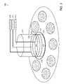
- FIG. 2illustrates a vapor phase epitaxy system 200 according to the present teachings that includes at least one electrode positioned in a flow of a first precursor gas and being substantially isolated from a flow of a second precursor gas.
- the VPE system 200is similar to the VPE system described in connection with FIG. 1 .
- the VPE system 200includes a process chamber 201 for containing process gasses.
- the VPE system 200includes a platen 202 , which is a disk-shaped substrate carrier that supports substrates 204 for vapor phase epitaxy.
- the VPE system 200includes a gas injector 206 comprising multiple regions that are separated by physical barriers and/or chemical barriers.
- the VPE system 200can include a first region 208 that is coupled to a first precursor gas source 210 and a second region 212 that is coupled to a second precursor gas source 214 .
- Any type of precursor gascan be used in the VPE system according to the present teachings.
- the gas injector 206can include additional regions that are separated by physical barriers and/or chemical barriers that may or may not be coupled to additional precursor and/or inert gas sources 211 .
- the first region 208 in the gas injector 206is positioned in quadrants of a disk and a second region 212 extends radially through the quadrants.
- the first and second regions 208 , 212 in the gas injector 206include a plurality of first and second regions that alternate across at least a portion of the gas injector 206 .
- the gas injector 206comprises liquid cooling channels to control a temperature of the gas injector 206 .
- a fluid coolant supply 216is coupled to liquid cooling channels in the flow injector 206 to circulate the cooling fluid in order to control the temperature of the gas injector 206 .
- the gas injector 206is designed to flow the first and second precursor gases over the platen 202 that supports the substrates 204 with either a laminar flow or a non-laminar flow. Also, in various embodiments, the gas injector 206 flows the first and second precursor gases in various directions relative to the platen 202 that supports the substrates 204 . For example, in some VPE systems according to the present invention, the gas injector 206 flows at least one of the first and second precursor gases in a direction that is perpendicular to the surface of platen 202 that supports the substrates 204 .
- the gas injector 206flows at least one of the first and second precursor gases in a direction that is parallel to the platen 202 that supports the substrates 204 .
- the gas injector 206flows one of the first and second precursor gases in a direction that is substantially parallel to the platen 202 that supports the substrates 204 and the other of the first and second precursor gases through the gas injector 206 in a direction that is substantially perpendicular to the platen 202 that supports the substrates 204 .
- Electrodes 218 , 219are positioned in the first region 212 so that first precursor gas flows in contact with or in close proximity to the electrodes 218 , 219 .
- the electrodes 218 , 219are positioned so that they are substantially isolated from the flow of the second precursor gas.
- the electrodes 218 , 219can be oriented in numerous ways.
- the electrodes 218 , 219can be oriented in a plane of the gas injector 206 (e.g. electrode 218 ).
- the electrodes 218 , 219can also be oriented perpendicular to the plane of the gas injector 206 (e.g. electrode 219 ).
- the electrodes 218 , 219can be positioned anywhere between the gas injector 206 and the platen 202 that supports the substrates 204 including in close proximity to the gas injector 206 and in close proximity to the platen 202 that supports the substrates 204 .
- the electrodes 218 , 219can be formed of any type of electrode material. However, the electrodes 218 , 219 are typically formed of a material that is resistant to corrosion so that they do not introduce any contamination into the VPE system 200 . Also, in various embodiments, any type of electrode configuration can be used including any number of electrodes, which can include only one electrode. In addition, in various embodiments, the electrodes 218 , 219 can be formed in any shape.
- the VPE system 200shows two different types of electrodes, a linear (straight) electrode 218 and a non-linear electrode 219 , such as a coiled electrode or other structure that increases or maximizes the surface area of the electrode that is exposed to the first precursor gas. In many systems, the same type of electrode is used, but in some systems two or more different types of electrodes are used.
- the electrodes 218 , 219are electrically active. In the embodiment shown in FIG. 2 , the electrodes 218 , 219 are at a floating potential when not powered. An output of a power supply 220 is electrically connected to the electrodes 218 , 219 . The power supply 220 generates a current that heats the electrodes 218 , 219 so as to thermally activate at least some of the first precursor gas molecules flowing in contact with or proximate to the electrodes 218 , 219 .
- the gas injector 206includes one or more baffles 222 or other types of physical structure that physically separates the first region 208 from the second region 212 so as to isolate the electrodes 218 , 219 from the flow of the second precursor gas.
- the one or more baffles 222are formed of non-thermally conductive materials so that the thermal profile in the process chamber 201 does not significantly change from thermal radiation emitted by the baffles 222 .
- the one or more baffles 222are shaped to preserve laminar flow of at least one of the first and second precursor gases across the platen 202 that supports the substrates 204 .
- the electrodes 218 , 219are formed of a catalytic material.
- a heatercan be positioned in thermal communication with the catalytic material so as to increase a reaction rate of the catalytic material.
- the electrodes 218 , 219are formed of a catalytic material including at least one of rhenium, tungsten, niobium, tantalum, and molybdenum.
- the electrodes 218 , 219can be formed of refractory and/or transition metals.
- a method of operating a vapor phase epitaxy systemincludes injecting a first precursor gas for vapor phase epitaxy in the first region 208 proximate to a platen 202 supporting substrates 204 and injecting a second precursor gas for vapor phase epitaxy in a second region 212 proximate to the platen 202 supporting substrates.
- the first and second precursor gasesare injected in a plurality of respective alternating first and second regions as described in connection with FIG. 4A .
- the first precursor gascan be a hydride precursor gas, such as NH 3 and the second precursor gas can be an organometalic precursor gas, such as trimethyl gallium, that is used to grow GaN by VPE.
- the first precursor gascan be a hydride precursor gas, such as NH 3 and the second precursor gas can be a metal halide precursor gas, such as gallium chloride, that is used to grow GaN by VPE.
- three precursor gasesare used.
- the first precursor gascan be a hydride precursor gas, such as NH 3
- the second precursor gascan be an organometalic precursor gas, such as trimethyl gallium.
- the third precursor gascan be a halide precursor gas, such as HCl. With these three precursor gases, the halide precursor gas and the organometallic precursor gas react to form a metal halide.
- the gas injector 206can include a third region for injecting the third precursor gas. Alternatively, the third precursor gas can be injected in the either the first or the second regions 208 , 212 .
- the first and second precursor gasescan be injected at any angle including perpendicular and parallel to the platen 202 supporting substrates 204 .
- the angle of injection for the second precursor gascan be the same as or different from the angle of injection of the first precursor gas.
- First precursor gas moleculesflow in contact with or in close proximity to the electrodes 218 , 219 .
- the electrodes 218 , 219are at least partially isolated from the flow of the injected second precursor gas.
- the electrodes 218 , 219are then electrically activated.
- the electrodes 218 , 219are isolated from a flow of the injected second precursor gas with physical baffles 222 .
- the baffles 222can be performed so as to preserves laminar flow over the platen 202 supporting substrates 204 as described in connection with FIG. 6 .
- inert gasesare injected in regions that isolate the electrodes 218 , 219 from a flow of the second precursor gas.
- inert gasrefers to a gas which does not substantially participate in the growth reactions. Inert gases are often mixed with the precursor gases. Such inert gases are referred to in the art as “carrier gases.”
- carrier gasesFor example, when growing III-V semiconductor materials, gases, such as N2, H2, He or mixtures thereof, are commonly used as carrier gases for precursor gases.
- the power supply 220generates a current that flows through the electrodes 218 , 219 so that the electrodes 218 , 219 generates heat that thermally activates the first precursor gas molecules without activating a substantial amount of second precursor gas molecules.
- the heated electrodes 218 , 219transfer energy to the first precursor gas molecules by various mechanisms including thermionic emission of electrons and interaction of the electrons with the reactant species.
- the electronsdo not have sufficient energy to ionize the reactant species.
- One example where the electrons do not have sufficient energy to ionize the reactant speciesis ionizing NH 3 . In methods that ionize NH 3 , the electrons interact with the reactant species so as to promote the species to a higher energy state.
- the electrodes 218 , 219are catalytic electrodes, which are formed of a catalytic material capable of catalyzing the first precursor gas if conditions are favorable.
- the catalytic electrodecan be heated with a separate heater to enhance the catalytic reaction.
- such a catalytic electrodeis useful to decompose NH 3 close to the gas injector 206 surface because it is far from the platen 202 supporting the substrate 204 and, therefore, may not have enough thermal energy for decomposition.
- Using a catalytic electrodelowers the activation energy for decomposition and, therefore, increases the probability of NH 3 decomposition even in regions of the process chamber 201 that have relatively low temperatures (i.e.
- the catalytic electrodeallows the reaction to proceed or, if the reaction was inclined to occur, to proceed more rapidly by lowering the activation energy of the reaction or having the reaction proceed through a different reaction pathway.
- the catalytic electrodeis positioned proximate to the boundary layer region 126 ( FIG. 1 ) so that the first precursor gas mixes with the second precursor gas shortly after the first precursor gas interacts with the catalytic electrode.
- VPE systemsinclude a catalytic electrode that is not energized. This is a catalytic electrode that is not powered by a power supply and that uses only the catalytic material and ambient heat to enhance the catalytic reaction.
- a catalytic electrodecan be positioned anywhere in the process chamber 201 . In some of these VPE systems, the catalytic electrode is positioned proximate to the platen 202 . Catalytic electrodes positioned proximate to the platen 202 can reach effective catalytic activity through secondary heating from the platen 202 alone.
- Slab-like streams of thermally activated first precursor gas moleculesflow generally downstream toward the platen 202 and substrates 204 in a flow region 224 of the reaction chamber 201 between the gas injector 206 and the platen 202 .
- the downward flowdoes not result in substantial mixing between separate streams of downwardly flowing gas. It is sometimes desirable to design and operate the system 200 so that there is laminar flow in the flow region 224 .
- the platen 202is rotated rapidly about the axis 104 with the rotary drive 106 so that the surface of the platen 202 and the surfaces of the substrates 204 are moving rapidly.
- the rapid motion of the platen 202 and substrates 204entrains the gases into rotational motion about axis 104 .
- the process gasesflow radially away from axis 104 , thereby causing the process gases in the various streams to mix with one another within a boundary layer that is schematically indicated in boundary layer region 126 .
- the activated first precursor gas molecules and the second precursor gas molecules in the mixture within the boundary layerflow over the surface of the substrates 204 , thereby reacting to form a VPE film.
- precursor gassesare introduced into the process chamber 201 at a relatively low temperature, and hence have low available energy, typically well below the energy required to induce rapid reaction of the reactants on the surface of the substrate 204 .
- most of the heating, and hence most of the increase in available energy of the reactantsoccurs within the boundary layer region 126 .
- substantially all of the heatingdepends upon the temperature of the substrate 204 and platen 202 .
- substantial energyis supplied to at least one precursor gas other than energy applied by heat transfer from the substrate, platen, and chamber walls.
- the location where the energy is appliedcan be controlled. For example, by applying the energy to the first precursor gas near the transition between the flow region 124 ( FIG. 1 ) and the boundary layer region 126 , the time between the moment when a given portion of a first precursor gas reaches a high available energy and the time when that portion encounters the substrate surface can be minimized.
- Such controlcan help to minimize undesired side reactions.
- ammonia having high available energymay spontaneously decompose into species such as NH 2 and NH, and then these species in turn may decompose to monatomic nitrogen, which very rapidly forms N 2 .
- Nitrogenis essentially unavailable for reaction with a metal organic.
- the desired reactions which deposit the semiconductor at the surfacesuch as reaction of the excited NH 3 with the metal organic or reaction of NH 2 or NH species with the metal organic at the substrate surface can be enhanced, whereas the undesirable side reaction can be suppressed.
- one feature of the present teachingsis that by using the electrodes according to the present invention, the operator has the ability to control the available energy of at least one precursor gas independently of the temperature of the substrates 204 .
- the available energy of at least one precursor gas in the boundary layer region 126can be increased without increasing the temperature of the substrates 204 and the platen 202 .
- the substrates 204 and the platen 202can be maintained at a lower temperature while still maintaining an acceptable level of available energy.
- FIG. 3illustrates a top-view of one embodiment of a disk-shaped gas injector 300 according to the present teaching which includes a first region 302 that is positioned in quadrants of the gas injector 300 and a second region 304 extending radially through the quadrants.
- the top-view shown in FIG. 3is presented looking upstream toward the precursor gas inlets in the gas injector 300 .
- the disk-shaped gas injector 300includes mechanical or chemical barriers 305 that isolate the first and second regions 302 , 304 .
- the mechanical or chemical barriers 305can be physical structures, such as baffles and/or gas curtains that inject inert gases to isolate the first and second regions 302 , 304 .
- FIG. 3shows electrodes 306 , 308 in two quadrants for clarity.
- electrodes 306 , 308are positioned in each of the quadrants of the first region 302 .
- each of the electrodes 306 , 308is suspended with an insulating support structure so that the electrodes 306 , 308 are electrically floating and easily connected to the power supply 220 ( FIG. 2 ).
- the electrodescan be linear (straight) electrodes or non-linear electrodes, such as coiled electrodes or other structures that increases or maximizes the surface area of the electrodes 306 , 308 that are exposed to the first precursor gas.
- the same type of electrodeis used throughout the first region 302 , but in some systems two or more different types of electrodes are used in different positions in the first region 302 .
- the type of electrode near the second region 304can be different from the type of electrode in the middle of the first region 302 .
- FIG. 3shows a first type of electrode 306 , which can be either linear or non-linear, positioned in the plane of the first precursor gas flow.
- FIG. 3shows a second type of electrode 308 positioned in the plane of the gas injector 300 .
- FIG. 3shows the second type of electrode 308 in a linear pattern.
- the second type of electrodecan also be formed in a non-linear pattern, such as a coil.
- the electrodes 306 , 308are positioned far enough from the second region 304 so that the chemical potential of the second precursor is not changed based on its proximity to the electrodes 306 , 308 . In other words, the electrodes 306 , 308 have essentially no interaction with the second precursor gas.
- One feature of the VPE system of the present teachingsis that the first and second precursor gases can be injected at the same distance from the substrate 204 ( FIG. 2 ). In other words, the second precursor gas does not have to be injected below the first precursor gas in the process chamber 201 to avoid activation. Injecting both the first and the second precursor gases at the same level in the process chamber 201 is important in many VPE processes because such injection can achieve laminar flow over large areas in vertical flow VPE process chambers. Laminar flow is desirable for many VPE processes because it improves uniformity.
- Methods of operating VPE systemscomprising the gas injector 300 of FIG. 3 include injecting the first precursor gas in the quadrants of the first region 302 so that first precursor gas molecules contact the electrodes 306 , 308 .
- the electrodes 306 , 308are powered with power supply 220 ( FIG. 2 ) so that they thermally activate the first precursor gas molecules.
- the first precursor gascan be a hydride precursor gas precursor gas admixture with a carrier gas.
- the second precursor gasis injected in the second region 304 adjacent to the electrodes 306 , 308 .
- the second precursor gascan be an organometallic admixture with a carrier gas such as nitrogen.
- Process conditionsare chosen so that the second precursor gas does not flow close enough to the electrodes 306 , 308 to be thermally activated by heat generated by the electrodes.
- the activated first precursor gas molecules and the second precursor gas moleculesthen flow over the surface of the substrates 204 ( FIG. 2 ), thereby reacting to form a VPE film.
- FIG. 4Aillustrates a cross-section of one embodiment of a disk-shaped gas injector 400 according to the present teaching that includes a plurality of first and second regions 402 , 404 which alternates across the gas injector 400 .
- the top-view shown in FIG. 4Ais presented looking upstream toward the precursor gas inlets in the gas injector 400 .
- the plurality of first regions 402includes gas inlets for injecting hydride or halide precursor gases with a carrier gas.
- the plurality of second regions 404includes gas inlets for injecting organometallic gases with a carrier gas.
- the area of the first regions 402is larger than the area of the second regions 404 .
- the flow rates of the first and second precursor gases and of the carrier gases during operationcan be adjusted for the particular dimensions of the first and the second regions 402 , 404 so that the desired volumes and concentrations of precursor gases flow across the substrates 204 ( FIG. 2 ) being processed.
- the gas injector 400includes a plurality of electrodes 406 , 408 positioned in the plurality of first regions 402 .
- the plurality of electrodes 406 , 408are positioned in the first region 402 or as far from the flow of the second precursor gas as possible so as to minimize the activation of second precursor gas molecules with the electrodes 406 , 408 .
- FIG. 4Aillustrates electrodes 406 , 408 in two different orientations. Electrodes are only shown in a few sections of the plurality of first regions 402 for clarity. In many VPE systems according to the present teachings, electrodes 406 , 408 are positioned in each of the plurality of the first regions 402 .
- each of the electrodes 406 , 408is suspended with an insulating support structure so that the electrodes 406 , 408 are electrically floating and easily connected to the power supply 220 ( FIG. 2 ).
- the electrodes 406 , 408can be linear (straight) electrodes or non-linear electrodes, such as coiled electrodes or other structures that increases or maximizes the surface area of the electrodes 406 , 408 that are exposed to the first precursor gas.
- FIG. 4Ashows a first type of electrode 406 , which can be either linear or non-linear, positioned in the plane of the first precursor gas flow.
- FIG. 4Ashows a second type of electrode 408 positioned in the plane of the gas injector 400 .
- FIG. 4Ashows the second type of electrode 408 as a non-linear electrode that can also be coiled.
- the second type of electrode 408can also be a linear electrode.
- FIG. 4Billustrates an expanded view of the disk-shaped gas injector 400 illustrating mechanical or chemical barriers 405 that isolate the electrodes 406 ( FIG. 4A ), 408 from the second precursor gas.
- the mechanical or chemical barriers 405isolate the electrodes 406 , 408 in first region 402 from the precursor gas flowing in the second region 404 .
- the barriers 405can be a physical structure, such as baffle.
- the barriers 405can be a gas curtains that inject inert gases between the first and second regions 402 , 404 as described herein.
- Methods of operating VPE systemscomprising the gas injector 400 of FIGS. 4A and 4B include injecting the first precursor gas in the plurality of first regions 402 so that first precursor gas molecules contact the electrodes 406 , 408 .
- the electrodes 406 , 408are powered with the power supply 220 ( FIG. 2 ) so that they thermally activate the first precursor gas molecules.
- the first precursor gascan be a hydride precursor gas admixture with a carrier gas that is thermally activated when it flows in contact with the electrodes 406 , 408 .
- the second precursor gasis injected in the plurality of second regions 404 .
- the second precursor gascan be an organometallic admixture with a carrier gas.
- Process conditionsare chosen so that the second precursor gas does not flow close enough to the electrodes 406 , 408 to be thermally activated by heat generated by the electrodes 406 , 408 .
- the activated first precursor gas molecules and the second precursor gas moleculesthen flow over the surface of the substrates 204 ( FIG. 2 ), thereby reacting to form a VPE film.
- FIG. 5illustrates a perspective top-view of a VPE system 500 according to the present teachings that includes a horizontal flow gas injector 502 .
- the VPE system 500is similar to the VPE system 200 that was described in connection with FIG. 2 .
- the VPE system 500includes circular gas injectors 504 , 506 , and 508 that inject precursor gases and inert gases in the plane of the platen 510 (i.e. horizontal flow into the process chamber).
- the first circular gas injector 504is coupled to a first precursor gas source 512 .
- the second circular gas injector 506is coupled to an inert gas source 514 .
- the third circular gas injector 508is coupled to a second precursor gas source 516 .
- the first and third circular gas injectors 504 , 508are also coupled to a carrier gas source.
- the first circular gas injector 504injects the first precursor gas in a first horizontal region 518 .
- the third circular gas injector 508injects the second precursor gas in a second horizontal region 520 .
- a circular electrode 522is positioned in the first horizontal region 518 so that first precursor gas molecules flow in contact with or proximate to the circular electrode 522 .
- a physical or chemical barriercan be positioned between the first and the second horizontal regions 518 , 520 in order to isolate the circular electrode 522 from the flow of the second precursor gas molecules.
- a baffleis positioned above the circular electrode 522 to substantially prevent the first precursor gas molecules from being thermally activated by the electrode 522 as they flow to the platen 510 .
- a gas curtainis used to separate the first and the second horizontal regions 518 and 520 .
- the second circular gas injector 506injects inert gas between the first and the second horizontal regions 518 , 520 in a pattern that substantially prevents the second precursor gas molecules from being activated by the circular electrode 522 .
- Methods of operating the VPE system 500 of FIG. 5include injecting the first precursor gas with the first circular gas injectors 504 and injecting the second precursor gas with the third circular gas injectors 508 .
- An inert gasis injected between the first and the second horizontal regions 518 , 520 with the second circular gas injectors 506 to form a chemical barrier that prevents the second precursor gas molecules from being activated by the circular electrode 522 .
- the circular electrode 522is powered by a power supply 220 ( FIG. 2 )
- the circular electrode 522thermally activates first precursor gas molecules injected by the first circular gas injector 504 that flow in contact with or in close proximity to the circular electrode 522 .
- the activated first precursor gas molecules and the second precursor gas moleculesthen flow over the surface of the substrates 524 , thereby reacting to form a VPE film.
- FIG. 6illustrates a foil-shaped electrode 600 positioned close to the surface of the platen 602 for thermally activating a precursor gas in a VPE system according to the present teaching.
- the electrode 600is positioned close to the surface of the platen 602 and substrate 604 being processed.
- the electrode 600 shown in FIG. 6is shaped as an airfoil in order to provide a laminar or near laminar flow of precursor gases across the surface of the substrate 604 .
- the electrode 600can be shaped to provide a relatively large surface area for the catalytic reaction.
Landscapes
- Chemical & Material Sciences (AREA)
- Engineering & Computer Science (AREA)
- Materials Engineering (AREA)
- Metallurgy (AREA)
- Organic Chemistry (AREA)
- General Chemical & Material Sciences (AREA)
- Chemical Kinetics & Catalysis (AREA)
- Mechanical Engineering (AREA)
- Inorganic Chemistry (AREA)
- Crystallography & Structural Chemistry (AREA)
- Physics & Mathematics (AREA)
- Optics & Photonics (AREA)
- Health & Medical Sciences (AREA)
- Toxicology (AREA)
- Condensed Matter Physics & Semiconductors (AREA)
- General Physics & Mathematics (AREA)
- Manufacturing & Machinery (AREA)
- Computer Hardware Design (AREA)
- Microelectronics & Electronic Packaging (AREA)
- Power Engineering (AREA)
- Plasma & Fusion (AREA)
- Chemical Vapour Deposition (AREA)
- Crystals, And After-Treatments Of Crystals (AREA)
Abstract
Description
- This application claims priority to U.S. Provisional Patent Application Ser. No. 61/195,093 filed Oct. 3, 2008, entitled “Chemical Vapor Deposition with Energy Input,” the entire application of which is incorporated herein by reference.
- The section headings used herein are for organizational purposes only and should not to be construed as limiting the subject matter described in the present application in any way.
- Vapor phase epitaxy (VPE) is a type of chemical vapor deposition (CVD) which involves directing one or more gases containing chemical species onto a surface of a substrate so that the reactive species react and form a film on the surface of the substrate. For example, VPE can be used to grow compound semiconductor material on a substrate. The substrate is typically a crystalline material in the form of a disc, which is commonly referred to as a “wafer.” Materials are typically grown by injecting at least a first and a second precursor gas into a process chamber containing the crystalline substrate.
- Compound semiconductors, such as III-V semiconductors, can be formed by growing various layers of semiconductor materials on a substrate using a hydride precursor gas and an organometalic precursor gas. Metalorganic vapor phase epitaxy (MOVPE) is a vapor deposition method that is commonly used to grow compound semiconductors using a surface reaction of metalorganics and metal hydrides containing the required chemical elements. For example, indium phosphide could be grown in a reactor on a substrate by introducing trimethylindium and phosphine. Alternative names for MOVPE used in the art include organometallic vapor phase epitaxy (OMVPE), metalorganic chemical vapor deposition (MOCVD), and organometallic chemical vapor deposition (OMCVD). In these processes, the gases are reacted with one another at the surface of a substrate, such as a sapphire, Si, GaAs, InP, InAs or GaP substrate, to form a III-V compound of the general formula InXGaYAlZNAAsBPCSbD, where X+Y+Z equals approximately one, and A+B+C+D equals approximately one, and each of X, Y, Z, A, B, C, and D can be between zero and one. In some instances, bismuth may be used in place of some or all of the other Group III metals.
- Compound semiconductors, such as III-V semiconductors, can also be formed by growing various layers of semiconductor materials on a substrate using a hydride or a halide precursor gas process. In one halide vapor phase epitaxy (HVPE) process, Group III nitrides (e.g., GaN, AN) are formed by reacting hot gaseous metal chlorides (e.g., GaCl or AlCl) with ammonia gas (NH3). The metal chlorides are generated by passing hot HCl gas over the hot Group III metals. All reactions are done in a temperature controlled quartz furnace. One feature of HVPE is that it can have a very high growth rate, up to 100 μm per hour for some state-of-the-art processes. Another feature of HVPE is that it can be used to deposit relatively high quality films because films are grown in a carbon free environment and because the hot HCl gas provides a self-cleaning effect.
- In these processes, the substrate is maintained at an elevated temperature within a reaction chamber. The precursor gases are typically mixed with inert carrier gases and are then directed into the reaction chamber. Typically, the gases are at a relatively low temperature when they are introduced into the reaction chamber. As the gases reach the hot substrate, their temperature, and hence their available energy for reaction, increases. Formation of the epitaxial layer occurs by final pyrolysis of the constituent chemicals at the substrate surface. Crystals are formed by a chemical reaction and not by physical deposition processes. Growth occurs in the gas phase at moderate pressures. Consequently VPE is a desirable growth technique for thermodynamically metastable alloys. Currently, VPE is commonly used for manufacturing laser diodes, solar cells, and LEDs.
- The present teaching, in accordance with preferred and exemplary embodiments, together with further advantages thereof, is more particularly described in the following detailed description, taken in conjunction with the accompanying drawings. The skilled person in the art will understand that the drawings, described below, are for illustration purposes only. The drawings are not necessarily to scale, emphasis instead generally being placed upon illustrating principles of the teaching. The drawings are not intended to limit the scope of the Applicant's teaching in any way.
FIG. 1 illustrates a known vapor phase epitaxy system used to form compound semiconductors.FIG. 2 illustrates a vapor phase epitaxy system according to the present teachings that includes at least one electrode positioned in a flow of a first precursor gas and being substantially isolated from a flow of a second precursor gas.FIG. 3 illustrates a top-view of one embodiment of a disk-shaped gas injector according to the present teaching that includes a first region that is positioned in quadrants of the gas injector and a second region extending radially through the quadrants.FIG. 4A illustrates a cross-section of one embodiment of a disk-shaped gas injector according to the present teaching that includes a plurality of first and second regions which alternates across the gas injector.FIG. 4B illustrates an expanded view of the disk-shaped gas injector illustrating mechanical or chemical barriers that isolate the electrodes from the second precursor gas.FIG. 5 illustrates a perspective top-view of a vapor phase epitaxy system according to the present teachings that includes a horizontal flow gas injector.FIG. 6 illustrates a foil-shaped electrode positioned close to the surface of the platen for thermally activating a precursor gas in a vapor phase epitaxy system according to the present teaching.- Reference in the specification to “one embodiment” or “an embodiment” means that a particular feature, structure, or characteristic described in connection with the embodiment is included in at least one embodiment of the teaching. The appearances of the phrase “in one embodiment” in various places in the specification are not necessarily all referring to the same embodiment.
- It should be understood that the individual steps of the methods of the present teachings may be performed in any order and/or simultaneously as long as the teaching remains operable. Furthermore, it should be understood that the apparatus and methods of the present teachings can include any number or all of the described embodiments as long as the teaching remains operable.
- The present teaching will now be described in more detail with reference to exemplary embodiments thereof as shown in the accompanying drawings. While the present teachings are described in conjunction with various embodiments and examples, it is not intended that the present teachings be limited to such embodiments. On the contrary, the present teachings encompass various alternatives, modifications and equivalents, as will be appreciated by those of skill in the art. Those of ordinary skill in the art having access to the teaching herein will recognize additional implementations, modifications, and embodiments, as well as other fields of use, which are within the scope of the present disclosure as described herein.
- The term “available energy” as used in the present disclosure refers to the chemical potential of a reactant species that is used in a chemical reaction. The chemical potential is a term commonly used in thermodynamics, physics, and chemistry to describe the energy of a system (particle, molecule, vibrational or electronic states, reaction equilibrium, etc.). However, more specific substitutions for the term chemical potential may be used in various academic disciplines, including Gibbs free energy (thermodynamics) and Fermi level (solid state physics), etc. Unless otherwise specified, references to the available energy should be understood as referring to the chemical potential of the specified material.
FIG. 1 illustrates a knownVPE system 100 used to form compound semiconductors. Thissystem 100 includes areaction chamber 101 having aspindle 102 mounted therein. Thespindle 102 is rotatable about anaxis 104 by arotary drive mechanism 106. Theaxis 104 extends in an upstream direction U and a downstream direction D as shown inFIG. 1 . Aplaten 108, which in many systems is a disc-like substrate carrier, is mounted on thespindle 102 for rotation therewith. Typically, theplaten 108 andspindle 102 rotate at rotation rates that are in the range of about 100-2,000 revolutions per minute. Theplaten 108 is adapted to hold a plurality of disc-like substrates 110 so thatsurfaces 112 of thesubstrates 110 are in a plane perpendicular toaxis 104 and face in the upstream direction U.- A
heater 114, such as a resistance heating element, is positioned within thereaction chamber 101 proximate to theplaten 108. Theheater 114 heats the substrate carrier to the desired processing temperature. Agas injector 116, which is sometimes known in the art as a flow inlet element, is mounted upstream of theplaten 108 andspindle 102. Thegas injector 116 is connected to processgas sources gas injector 116 directs streams of various process gases into thereaction chamber 101. Afluid coolant supply 117 is coupled to liquid cooling channels in theflow injector 116 to circulate the cooling fluid in order to control the temperature of thegas injector 116. - In operation, streams of process gases from the
process gas sources platen 108 andsubstrates 110 in a region of thereaction chamber 101 between thegas injector 116 and theplaten 108, that is referred to herein as the “flowregion 124.” In known systems, this downward flow does not result in substantial mixing between separate streams of downwardly flowing gas. It is typically desirable to design and operate thesystem 100 so that there is laminar flow in theflow region 124. In normal operation, theplaten 108 is rotated rapidly about theaxis 104 with therotary drive 106 so that the surface of theplaten 108 and the surfaces of thesubstrates 110 are moving rapidly. The rapid motion of theplaten 108 andsubstrates 110 entrains the gases into rotational motion aboutaxis 104. Consequently, the process gases flow radially away fromaxis 104, thereby causing the process gases in the various streams to mix with one another within a boundary layer that is schematically indicated inboundary layer region 126. - In practice, there is a gradual transition between the generally downstream gas flow indicated by
arrows 128 in theflow region 124 and the rapid rotational flow and mixing in theboundary layer 126. Nevertheless, theboundary layer 126 is generally regarded as a region in which the gas flow is substantially parallel to the surfaces of thesubstrates 110. In some methods of operation, the thickness of theboundary layer 126 is on order of about 1 cm and the distance from the downstream face ofgas injector 116 to thesurfaces 112 of thesubstrates 110 is about 5-8 cm. Thus, theflow region 124 occupies the major portion of the space between thegas injector 116 and theplaten 108. The rotational motion of theplaten 108 pumps the gases outwardly around the peripheral edges of theplaten 108, and hence the gases pass downstream to anexhaust system 130. In many methods of operation, thereaction chamber 101 is maintained under an absolute pressure from about 25-1,000 Ton. Many processes operate at an absolute pressure of about 50-760 Torr. - The
gas injector 116 is maintained at a relatively low temperature, which is typically about 60° C. or less, although higher temperatures are sometimes used. In Halide VPE systems, the Group III halide is maintained at an elevated temperature to prevent condensation. This elevated temperature is below the temperature of thesubstrates 110 where deposition occurs. The relatively low temperature is chosen to inhibit decomposition of reactants and/or to inhibit the formation of undesired reactions of the reactants in thegas injector 116 and in theflow region 124. Also, in many processes, thewalls 101′ ofreaction chamber 101 are cooled to about 25° C. in order to minimize the rate of any reactions of the process gases in theflow region 124 remote from theplaten 108. - It is desirable to promote rapid reactions between the gases in the
boundary layer 126 at the surfaces of thesubstrates 110 because the residence time of the gases in theboundary layer 126 is relatively brief. In a conventional VPE system, the reaction energy is provided primarily by heat from theplaten 108 andsubstrates 110. For example, in some processes, the reaction energy is the energy required to dissociate a Group V hydride, such as NH3, to form reactive intermediates, such as NH2and NH. However, increasing the temperature of theplaten 108 andsubstrates 110 also tends to increase dissociation of the deposited compound semiconductors. For example, increasing the temperature of theplaten 108 andsubstrates 110 can result in a loss of nitrogen from the semiconductor especially when growing Indium-rich compounds such as InGaN and InN. - In one aspect of the present teachings, VPE systems include one or more electrically active electrodes that are used to add additional energy to a process gas in order to increase the reaction rate or to modify the reaction chemistry. One skilled in the art will appreciate that any type of electrically active electrode can be used, such as wires and filaments in any shape, which are exposed to a process gas in the
process chamber 101. - In many embodiments of the present teachings, it is desirable to supply energy to one of the process gases without supplying significant energy to other process gases. For example, in many Group III-V deposition processes, it is desirable to apply additional energy to the Group V hydride precursor gases, which for example, can be ammonia (NH3) without supplying significant energy to the Group III metal precursor gases. One skilled in the art will appreciate that selective application of energy to one or more of process gases can be accomplished in numerous ways. For example, the one or more electrically active electrodes can be physically isolated from a precursor gas that will react in the presence of the elevated temperatures. Physical isolation can be achieved by introducing the gases separately in different regions of the reactor and by using baffles and/or gas curtains as described herein. One feature of the present teachings is that gases can be introduced separately, but at the same distance from the
substrates 110 in order to maintain laminar flow over the surfaces of thesubstrates 110. FIG. 2 illustrates a vaporphase epitaxy system 200 according to the present teachings that includes at least one electrode positioned in a flow of a first precursor gas and being substantially isolated from a flow of a second precursor gas. TheVPE system 200 is similar to the VPE system described in connection withFIG. 1 . TheVPE system 200 includes aprocess chamber 201 for containing process gasses. In addition, theVPE system 200 includes aplaten 202, which is a disk-shaped substrate carrier that supportssubstrates 204 for vapor phase epitaxy.- The
VPE system 200 includes agas injector 206 comprising multiple regions that are separated by physical barriers and/or chemical barriers. For example, theVPE system 200 can include afirst region 208 that is coupled to a firstprecursor gas source 210 and asecond region 212 that is coupled to a secondprecursor gas source 214. Any type of precursor gas can be used in the VPE system according to the present teachings. In various other embodiments, thegas injector 206 can include additional regions that are separated by physical barriers and/or chemical barriers that may or may not be coupled to additional precursor and/orinert gas sources 211. - As described herein, there are many possible gas injector designs that inject different precursor gases into different regions of the
process chamber 201. For example, in one embodiment that is described in connection withFIG. 3 , thefirst region 208 in thegas injector 206 is positioned in quadrants of a disk and asecond region 212 extends radially through the quadrants. In another embodiment that is described in connection withFIG. 4A , the first andsecond regions gas injector 206 include a plurality of first and second regions that alternate across at least a portion of thegas injector 206. In many practical embodiments, thegas injector 206 comprises liquid cooling channels to control a temperature of thegas injector 206. Afluid coolant supply 216 is coupled to liquid cooling channels in theflow injector 206 to circulate the cooling fluid in order to control the temperature of thegas injector 206. - In various embodiments, the
gas injector 206 is designed to flow the first and second precursor gases over theplaten 202 that supports thesubstrates 204 with either a laminar flow or a non-laminar flow. Also, in various embodiments, thegas injector 206 flows the first and second precursor gases in various directions relative to theplaten 202 that supports thesubstrates 204. For example, in some VPE systems according to the present invention, thegas injector 206 flows at least one of the first and second precursor gases in a direction that is perpendicular to the surface ofplaten 202 that supports thesubstrates 204. Also, in some VPE systems, thegas injector 206 flows at least one of the first and second precursor gases in a direction that is parallel to theplaten 202 that supports thesubstrates 204. In one particular, VPE system, thegas injector 206 flows one of the first and second precursor gases in a direction that is substantially parallel to theplaten 202 that supports thesubstrates 204 and the other of the first and second precursor gases through thegas injector 206 in a direction that is substantially perpendicular to theplaten 202 that supports thesubstrates 204. Electrodes first region 212 so that first precursor gas flows in contact with or in close proximity to theelectrodes electrodes electrodes electrodes electrodes electrodes gas injector 206 and theplaten 202 that supports thesubstrates 204 including in close proximity to thegas injector 206 and in close proximity to theplaten 202 that supports thesubstrates 204.- In various embodiments, the
electrodes electrodes VPE system 200. Also, in various embodiments, any type of electrode configuration can be used including any number of electrodes, which can include only one electrode. In addition, in various embodiments, theelectrodes VPE system 200 shows two different types of electrodes, a linear (straight)electrode 218 and anon-linear electrode 219, such as a coiled electrode or other structure that increases or maximizes the surface area of the electrode that is exposed to the first precursor gas. In many systems, the same type of electrode is used, but in some systems two or more different types of electrodes are used. - The
electrodes FIG. 2 , theelectrodes power supply 220 is electrically connected to theelectrodes power supply 220 generates a current that heats theelectrodes electrodes - One skilled in the art will appreciate that there are numerous ways of isolating the
electrodes gas injector 206 includes one ormore baffles 222 or other types of physical structure that physically separates thefirst region 208 from thesecond region 212 so as to isolate theelectrodes more baffles 222 are formed of non-thermally conductive materials so that the thermal profile in theprocess chamber 201 does not significantly change from thermal radiation emitted by thebaffles 222. In one embodiment, the one ormore baffles 222 are shaped to preserve laminar flow of at least one of the first and second precursor gases across theplaten 202 that supports thesubstrates 204. - In one embodiment, the
electrodes electrodes electrodes - A method of operating a vapor phase epitaxy system according to the present teachings includes injecting a first precursor gas for vapor phase epitaxy in the
first region 208 proximate to aplaten 202 supportingsubstrates 204 and injecting a second precursor gas for vapor phase epitaxy in asecond region 212 proximate to theplaten 202 supporting substrates. In one method, the first and second precursor gases are injected in a plurality of respective alternating first and second regions as described in connection withFIG. 4A . - Any type of VPE precursor gases can be used. For example, the first precursor gas can be a hydride precursor gas, such as NH3and the second precursor gas can be an organometalic precursor gas, such as trimethyl gallium, that is used to grow GaN by VPE. Also, the first precursor gas can be a hydride precursor gas, such as NH3and the second precursor gas can be a metal halide precursor gas, such as gallium chloride, that is used to grow GaN by VPE. In some methods, three precursor gases are used. For example in these methods, the first precursor gas can be a hydride precursor gas, such as NH3, and the second precursor gas can be an organometalic precursor gas, such as trimethyl gallium. The third precursor gas can be a halide precursor gas, such as HCl. With these three precursor gases, the halide precursor gas and the organometallic precursor gas react to form a metal halide. In methods using three precursor gases, the
gas injector 206 can include a third region for injecting the third precursor gas. Alternatively, the third precursor gas can be injected in the either the first or thesecond regions - The first and second precursor gases can be injected at any angle including perpendicular and parallel to the
platen 202 supportingsubstrates 204. The angle of injection for the second precursor gas can be the same as or different from the angle of injection of the first precursor gas. First precursor gas molecules flow in contact with or in close proximity to theelectrodes electrodes electrodes electrodes physical baffles 222. Thebaffles 222 can be performed so as to preserves laminar flow over theplaten 202 supportingsubstrates 204 as described in connection withFIG. 6 . - In methods using gas curtains, inert gases are injected in regions that isolate the
electrodes - The
power supply 220 generates a current that flows through theelectrodes electrodes heated electrodes - In some VPE systems according to the present teachings, the
electrodes gas injector 206 surface because it is far from theplaten 202 supporting thesubstrate 204 and, therefore, may not have enough thermal energy for decomposition. Using a catalytic electrode lowers the activation energy for decomposition and, therefore, increases the probability of NH3decomposition even in regions of theprocess chamber 201 that have relatively low temperatures (i.e. regions close to thegas injector 206 away from the substrate). The catalytic electrode allows the reaction to proceed or, if the reaction was inclined to occur, to proceed more rapidly by lowering the activation energy of the reaction or having the reaction proceed through a different reaction pathway. In one VPE system according to the present teachings, the catalytic electrode is positioned proximate to the boundary layer region126 (FIG. 1 ) so that the first precursor gas mixes with the second precursor gas shortly after the first precursor gas interacts with the catalytic electrode. - Other VPE systems according to the present teachings include a catalytic electrode that is not energized. This is a catalytic electrode that is not powered by a power supply and that uses only the catalytic material and ambient heat to enhance the catalytic reaction. In various VPE systems according to the present teachings, a catalytic electrode can be positioned anywhere in the
process chamber 201. In some of these VPE systems, the catalytic electrode is positioned proximate to theplaten 202. Catalytic electrodes positioned proximate to theplaten 202 can reach effective catalytic activity through secondary heating from theplaten 202 alone. - Slab-like streams of thermally activated first precursor gas molecules flow generally downstream toward the
platen 202 andsubstrates 204 in aflow region 224 of thereaction chamber 201 between thegas injector 206 and theplaten 202. In many methods according to the present teachings, the downward flow does not result in substantial mixing between separate streams of downwardly flowing gas. It is sometimes desirable to design and operate thesystem 200 so that there is laminar flow in theflow region 224. Theplaten 202 is rotated rapidly about theaxis 104 with therotary drive 106 so that the surface of theplaten 202 and the surfaces of thesubstrates 204 are moving rapidly. The rapid motion of theplaten 202 andsubstrates 204 entrains the gases into rotational motion aboutaxis 104. Consequently, the process gases flow radially away fromaxis 104, thereby causing the process gases in the various streams to mix with one another within a boundary layer that is schematically indicated inboundary layer region 126. The activated first precursor gas molecules and the second precursor gas molecules in the mixture within the boundary layer flow over the surface of thesubstrates 204, thereby reacting to form a VPE film. - In conventional VPE systems, precursor gasses are introduced into the
process chamber 201 at a relatively low temperature, and hence have low available energy, typically well below the energy required to induce rapid reaction of the reactants on the surface of thesubstrate 204. In conventional methods of VPE, there may be some heating of the reactants by radiant heat transfer as the reactants pass downstream from the inlet towards theboundary layer region 126. However, most of the heating, and hence most of the increase in available energy of the reactants, occurs within theboundary layer region 126. In these conventional VPE systems, substantially all of the heating depends upon the temperature of thesubstrate 204 andplaten 202. - In VPE systems according to the present teachings, substantial energy is supplied to at least one precursor gas other than energy applied by heat transfer from the substrate, platen, and chamber walls. The location where the energy is applied can be controlled. For example, by applying the energy to the first precursor gas near the transition between the flow region124 (
FIG. 1 ) and theboundary layer region 126, the time between the moment when a given portion of a first precursor gas reaches a high available energy and the time when that portion encounters the substrate surface can be minimized. Such control can help to minimize undesired side reactions. For example, ammonia having high available energy may spontaneously decompose into species such as NH2and NH, and then these species in turn may decompose to monatomic nitrogen, which very rapidly forms N2. Nitrogen is essentially unavailable for reaction with a metal organic. By applying the energy to the ammonia just before or just as the ammonia enters the boundary layer, the desired reactions which deposit the semiconductor at the surface, such as reaction of the excited NH3with the metal organic or reaction of NH2or NH species with the metal organic at the substrate surface can be enhanced, whereas the undesirable side reaction can be suppressed. - Thus, one feature of the present teachings is that by using the electrodes according to the present invention, the operator has the ability to control the available energy of at least one precursor gas independently of the temperature of the
substrates 204. Thus, the available energy of at least one precursor gas in the boundary layer region126 (FIG. 1 ) can be increased without increasing the temperature of thesubstrates 204 and theplaten 202. Conversely, thesubstrates 204 and theplaten 202 can be maintained at a lower temperature while still maintaining an acceptable level of available energy. FIG. 3 illustrates a top-view of one embodiment of a disk-shapedgas injector 300 according to the present teaching which includes afirst region 302 that is positioned in quadrants of thegas injector 300 and asecond region 304 extending radially through the quadrants. The top-view shown inFIG. 3 is presented looking upstream toward the precursor gas inlets in thegas injector 300. The disk-shapedgas injector 300 includes mechanical orchemical barriers 305 that isolate the first andsecond regions chemical barriers 305 can be physical structures, such as baffles and/or gas curtains that inject inert gases to isolate the first andsecond regions FIG. 3 showselectrodes electrodes first region 302. In some embodiments, each of theelectrodes electrodes FIG. 2 ). In various embodiments, the electrodes can be linear (straight) electrodes or non-linear electrodes, such as coiled electrodes or other structures that increases or maximizes the surface area of theelectrodes - In many systems, the same type of electrode is used throughout the
first region 302, but in some systems two or more different types of electrodes are used in different positions in thefirst region 302. For example, the type of electrode near the second region304 (at the edges of the first region302) can be different from the type of electrode in the middle of thefirst region 302. For the purpose of illustrating the positioning of different types of electrodes,FIG. 3 shows a first type ofelectrode 306, which can be either linear or non-linear, positioned in the plane of the first precursor gas flow. In addition,FIG. 3 shows a second type ofelectrode 308 positioned in the plane of thegas injector 300.FIG. 3 shows the second type ofelectrode 308 in a linear pattern. However, it should be understood that the second type of electrode can also be formed in a non-linear pattern, such as a coil. - The
electrodes second region 304 so that the chemical potential of the second precursor is not changed based on its proximity to theelectrodes electrodes FIG. 2 ). In other words, the second precursor gas does not have to be injected below the first precursor gas in theprocess chamber 201 to avoid activation. Injecting both the first and the second precursor gases at the same level in theprocess chamber 201 is important in many VPE processes because such injection can achieve laminar flow over large areas in vertical flow VPE process chambers. Laminar flow is desirable for many VPE processes because it improves uniformity. - Methods of operating VPE systems comprising the
gas injector 300 ofFIG. 3 include injecting the first precursor gas in the quadrants of thefirst region 302 so that first precursor gas molecules contact theelectrodes electrodes FIG. 2 ) so that they thermally activate the first precursor gas molecules. For example, the first precursor gas can be a hydride precursor gas precursor gas admixture with a carrier gas. The second precursor gas is injected in thesecond region 304 adjacent to theelectrodes electrodes FIG. 2 ), thereby reacting to form a VPE film. FIG. 4A illustrates a cross-section of one embodiment of a disk-shapedgas injector 400 according to the present teaching that includes a plurality of first andsecond regions gas injector 400. The top-view shown inFIG. 4A is presented looking upstream toward the precursor gas inlets in thegas injector 400. The plurality offirst regions 402 includes gas inlets for injecting hydride or halide precursor gases with a carrier gas. The plurality ofsecond regions 404 includes gas inlets for injecting organometallic gases with a carrier gas.- In many VPE systems according to the present teachings, the area of the
first regions 402 is larger than the area of thesecond regions 404. The flow rates of the first and second precursor gases and of the carrier gases during operation can be adjusted for the particular dimensions of the first and thesecond regions FIG. 2 ) being processed. - The
gas injector 400 includes a plurality ofelectrodes first regions 402. In many VPE systems according to the present invention, the plurality ofelectrodes first region 402 or as far from the flow of the second precursor gas as possible so as to minimize the activation of second precursor gas molecules with theelectrodes FIG. 4A illustrateselectrodes first regions 402 for clarity. In many VPE systems according to the present teachings,electrodes first regions 402. In some embodiments, each of theelectrodes electrodes FIG. 2 ). In various embodiments, theelectrodes electrodes - In many systems, the same type of electrode is used throughout the
first region 402, but in some systems two or more different types of electrodes are used in different positions in thefirst region 402. For the purpose of illustrating the positioning of different types of electrodes,FIG. 4A shows a first type ofelectrode 406, which can be either linear or non-linear, positioned in the plane of the first precursor gas flow. In addition,FIG. 4A shows a second type ofelectrode 408 positioned in the plane of thegas injector 400.FIG. 4A shows the second type ofelectrode 408 as a non-linear electrode that can also be coiled. However, it should be understood that the second type ofelectrode 408 can also be a linear electrode. FIG. 4B illustrates an expanded view of the disk-shapedgas injector 400 illustrating mechanical orchemical barriers 405 that isolate the electrodes406 (FIG. 4A ),408 from the second precursor gas. The mechanical orchemical barriers 405 isolate theelectrodes first region 402 from the precursor gas flowing in thesecond region 404. As described herein, thebarriers 405 can be a physical structure, such as baffle. In addition, thebarriers 405 can be a gas curtains that inject inert gases between the first andsecond regions - Methods of operating VPE systems comprising the
gas injector 400 ofFIGS. 4A and 4B include injecting the first precursor gas in the plurality offirst regions 402 so that first precursor gas molecules contact theelectrodes electrodes FIG. 2 ) so that they thermally activate the first precursor gas molecules. For example, the first precursor gas can be a hydride precursor gas admixture with a carrier gas that is thermally activated when it flows in contact with theelectrodes second regions 404. For example, the second precursor gas can be an organometallic admixture with a carrier gas. Process conditions are chosen so that the second precursor gas does not flow close enough to theelectrodes electrodes FIG. 2 ), thereby reacting to form a VPE film. FIG. 5 illustrates a perspective top-view of aVPE system 500 according to the present teachings that includes a horizontalflow gas injector 502. TheVPE system 500 is similar to theVPE system 200 that was described in connection withFIG. 2 . However, theVPE system 500 includescircular gas injectors - In the embodiment shown in
FIG. 5 , the firstcircular gas injector 504 is coupled to a firstprecursor gas source 512. The secondcircular gas injector 506 is coupled to aninert gas source 514. The thirdcircular gas injector 508 is coupled to a second precursor gas source516. In some VPE systems according to the present teachings, the first and thirdcircular gas injectors circular gas injector 504 injects the first precursor gas in a firsthorizontal region 518. The thirdcircular gas injector 508 injects the second precursor gas in a secondhorizontal region 520. - A
circular electrode 522 is positioned in the firsthorizontal region 518 so that first precursor gas molecules flow in contact with or proximate to thecircular electrode 522. A physical or chemical barrier can be positioned between the first and the secondhorizontal regions circular electrode 522 from the flow of the second precursor gas molecules. In some systems according to the present teachings, a baffle is positioned above thecircular electrode 522 to substantially prevent the first precursor gas molecules from being thermally activated by theelectrode 522 as they flow to theplaten 510. - In some systems according to the present teachings, a gas curtain is used to separate the first and the second
horizontal regions circular gas injector 506 injects inert gas between the first and the secondhorizontal regions circular electrode 522. - Methods of operating the
VPE system 500 ofFIG. 5 include injecting the first precursor gas with the firstcircular gas injectors 504 and injecting the second precursor gas with the thirdcircular gas injectors 508. An inert gas is injected between the first and the secondhorizontal regions circular gas injectors 506 to form a chemical barrier that prevents the second precursor gas molecules from being activated by thecircular electrode 522. When thecircular electrode 522 is powered by a power supply220 (FIG. 2 ), thecircular electrode 522 thermally activates first precursor gas molecules injected by the firstcircular gas injector 504 that flow in contact with or in close proximity to thecircular electrode 522. The activated first precursor gas molecules and the second precursor gas molecules then flow over the surface of thesubstrates 524, thereby reacting to form a VPE film. FIG. 6 illustrates a foil-shapedelectrode 600 positioned close to the surface of theplaten 602 for thermally activating a precursor gas in a VPE system according to the present teaching. Theelectrode 600 is positioned close to the surface of theplaten 602 andsubstrate 604 being processed. Theelectrode 600 shown inFIG. 6 is shaped as an airfoil in order to provide a laminar or near laminar flow of precursor gases across the surface of thesubstrate 604. In addition, in embodiments where theelectrode 600 is formed of a catalytic material, theelectrode 600 can be shaped to provide a relatively large surface area for the catalytic reaction.- While the applicant's teaching are described in conjunction with various embodiments, it is not intended that the applicant's teaching be limited to such embodiments. On the contrary, the applicant's teaching encompass various alternatives, modifications, and equivalents, as will be appreciated by those of skill in the art, which may be made therein without departing from the spirit and scope of the teaching.
Claims (37)
1. A vapor phase epitaxy system comprising:
a. a platen that supports substrates for vapor phase epitaxy;
b. a gas injector comprising a first region that is coupled to a first precursor gas source and a second region that is coupled to a second precursor gas source, the gas injector injecting the first precursor gas into the first region and injecting the second precursor gas into the second region;
c. at least one electrode that is positioned in the first region so that first precursor gas molecules flow proximate to the at least one electrode and positioned to be substantially isolated from a flow of the second precursor gas; and
d. a power supply having an output that is electrically connected to the at least one electrode, the power supply generating a current that heats the at least one electrode so as to thermally activate at least some of the first precursor gas molecules flowing proximate to the at least one electrode.
2. The system ofclaim 1 wherein the gas injector comprises liquid cooling channels to control a temperature of the gas injector.
3. The system ofclaim 1 wherein the first and second regions in the gas injector comprise a plurality of first and second regions that alternate across at least a portion of the gas injector.
4. The system ofclaim 1 wherein at least one of the first and second precursor gases flows through the gas injector in a direction that is perpendicular to the platen that supports the substrates.
5. The system ofclaim 1 wherein at least one of the first and second precursor gases flows through the gas injector in a direction that is parallel to the platen that supports the substrates.
6. The system ofclaim 1 wherein one of the first and second precursor gases flow through the gas injector in a direction that is substantially parallel to the platen that supports the substrates and the other of the first and second precursor gases flow through the gas injector in a direction that is substantially perpendicular to the platen that supports the substrates.
7. The system ofclaim 1 wherein the gas injector flows the first and second precursor gases over the platen with a laminar flow.
8. The system ofclaim 1 wherein the gas injector flows the first and second precursor gas over the platen with a non-laminar flow.
9. The system ofclaim 1 wherein the gas injector further comprises a baffle that physically separates the first and the second regions.
10. The system ofclaim 9 wherein the baffle is shaped to preserve laminar flow of the first and second precursor gases across the platen that supports the substrates.
11. The system ofclaim 9 wherein the baffle is formed of a non-thermally conductive material.
12. The system ofclaim 1 wherein the at least one electrode is formed of a catalytic material.
13. The system ofclaim 12 wherein the catalytic material comprises at least one of tungsten, rhenium, and molybdenum.
14. The system ofclaim 1 further comprising a catalytic electrode positioned proximate to the platen.
15. The system ofclaim 1 wherein the electrode is formed in a non-linear structure.
16. The system ofclaim 1 wherein the electrode is oriented in a plane of the gas injector.
17. The system ofclaim 1 wherein the electrode is oriented in a plane that is perpendicular to the gas injector.
18. The system ofclaim 1 wherein the electrode is positioned proximate to the platen.
19. A method of vapor phase epitaxy, the method comprising:
a. injecting a first precursor gas for vapor phase epitaxy in a first region proximate to a platen supporting substrates;
b. injecting a second precursor gas for vapor phase epitaxy in a second region proximate to the platen supporting substrates;
c. positioning an electrode in a flow of the injected first precursor gas;
d. isolating the electrode from a flow of the injected second precursor gas; and
e. activating the first precursor gas with the electrode.
20. The method ofclaim 19 wherein the activating the first precursor gas generates first precursor gas radicals.
21. The method ofclaim 19 wherein the activating the first precursor gas comprises energizing the electrode to thermally activate the first precursor gas.
22. The method ofclaim 19 wherein the activating the first precursor gas comprises catalytically activating the first precursor gas with a catalytic electrode material.
23. The method ofclaim 19 wherein the injecting the first precursor gas comprises injecting a hydride precursor gas and the injecting the second precursor gas comprises injecting an organometalic precursor gas.
24. The method ofclaim 23 further comprising injecting a halide precursor gas.
25. The method ofclaim 19 wherein the injecting the first precursor gas for vapor phase epitaxy comprises injecting a hydride precursor gas and the injecting the second precursor gas for vapor phase epitaxy comprises injecting an metal halide precursor gas.
26. The method ofclaim 19 wherein the injecting the first and second precursor gases for vapor phase epitaxy comprise injecting the first and second precursor gases parallel to the platen supporting substrates.
27. The method ofclaim 19 wherein the injecting the first and second precursor gases for vapor phase epitaxy comprise injecting the first and second precursor gases perpendicular to the platen supporting substrates.
28. The method ofclaim 19 wherein the injecting the first and second precursor gases for vapor phase epitaxy comprise injecting one of the first and second precursor gases perpendicular to the platen supporting substrates and injecting the other of the first and second precursor gases parallel to the platen supporting substrates.
29. The method ofclaim 19 wherein the injecting the first and second precursor gases comprise injecting the first and second precursor gases in a plurality of alternating first and second regions wherein the first precursor gas is injected in the first regions and the second precursor gas is injected in the second regions of the plurality of alternating first and second regions.
30. The method ofclaim 19 wherein the isolating the electrode from a flow of the injected second precursor gas comprises baffling the electrode.
31. The method ofclaim 30 wherein the baffling preserves laminar flow over the platen supporting substrates.
32. A vapor phase epitaxy system comprising:
a. a means for injecting a first precursor gas for vapor phase epitaxy in a first region proximate to a platen supporting substrates;
b. a means for injecting a second precursor gas for vapor phase epitaxy in a second region proximate to the platen supporting substrates;
c. an electrode positioned in a flow of the injected first precursor gas;
d. a means for isolating the electrode from a flow of the injected second precursor gas; and
e. a means for activating the first precursor gas with the electrode.
33. The system ofclaim 32 wherein the means for activating the first precursor gas with the electrode comprises energizing the electrode.
34. The system ofclaim 32 wherein the means for activating the first precursor gas with the electrode comprises forming a catalytic reaction with the electrode.
35. The system ofclaim 32 wherein the means for isolating the electrode from a flow of the injected second precursor gas comprises baffling the electrode.
36. A method of vapor phase epitaxy, the method comprising:
a. injecting a first precursor gas comprising H2and N2for vapor phase epitaxy in a first region proximate to a platen supporting substrates;
b. injecting a second precursor gas for vapor phase epitaxy in a second region proximate to the platen supporting substrates;
c. positioning a catalytic electrode in a flow of the injected first precursor gas;
d. isolating the electrode from a flow of the injected second precursor gas; and
e. energizing the catalytic electrode to activate the first precursor gas to generate at least one of NH2and NH.
37. The method ofclaim 36 further comprising positioning a second catalytic electrode in thermal communication with the platen supporting substrates that is not energized.
Priority Applications (1)
| Application Number | Priority Date | Filing Date | Title |
|---|---|---|---|
| US12/572,245US20100086703A1 (en) | 2008-10-03 | 2009-10-01 | Vapor Phase Epitaxy System |
Applications Claiming Priority (2)
| Application Number | Priority Date | Filing Date | Title |
|---|---|---|---|
| US19509308P | 2008-10-03 | 2008-10-03 | |
| US12/572,245US20100086703A1 (en) | 2008-10-03 | 2009-10-01 | Vapor Phase Epitaxy System |
Publications (1)
| Publication Number | Publication Date |
|---|---|
| US20100086703A1true US20100086703A1 (en) | 2010-04-08 |
Family
ID=41429649
Family Applications (4)
| Application Number | Title | Priority Date | Filing Date |
|---|---|---|---|
| US12/572,245AbandonedUS20100086703A1 (en) | 2008-10-03 | 2009-10-01 | Vapor Phase Epitaxy System |
| US13/121,371AbandonedUS20110174213A1 (en) | 2008-10-03 | 2009-10-01 | Vapor Phase Epitaxy System |
| US12/587,228Expired - Fee RelatedUS8815709B2 (en) | 2008-10-03 | 2009-10-02 | Chemical vapor deposition with energy input |
| US14/330,433AbandonedUS20140318453A1 (en) | 2008-10-03 | 2014-07-14 | Chemical vapor deposition with energy input |
Family Applications After (3)
| Application Number | Title | Priority Date | Filing Date |
|---|---|---|---|
| US13/121,371AbandonedUS20110174213A1 (en) | 2008-10-03 | 2009-10-01 | Vapor Phase Epitaxy System |
| US12/587,228Expired - Fee RelatedUS8815709B2 (en) | 2008-10-03 | 2009-10-02 | Chemical vapor deposition with energy input |
| US14/330,433AbandonedUS20140318453A1 (en) | 2008-10-03 | 2014-07-14 | Chemical vapor deposition with energy input |
Country Status (8)
| Country | Link |
|---|---|
| US (4) | US20100086703A1 (en) |
| EP (2) | EP2332167A4 (en) |
| JP (2) | JP2012504873A (en) |
| KR (2) | KR20110079831A (en) |
| CN (2) | CN102171795A (en) |
| SG (1) | SG194408A1 (en) |
| TW (2) | TWI411700B (en) |
| WO (2) | WO2010040011A2 (en) |
Cited By (320)
| Publication number | Priority date | Publication date | Assignee | Title |
|---|---|---|---|---|
| US20150361582A1 (en)* | 2014-06-17 | 2015-12-17 | Veeco Instruments, Inc. | Gas Flow Flange For A Rotating Disk Reactor For Chemical Vapor Deposition |
| US20180174826A1 (en)* | 2016-12-15 | 2018-06-21 | Asm Ip Holding B.V. | Sequential infiltration synthesis apparatus |
| US10559458B1 (en) | 2018-11-26 | 2020-02-11 | Asm Ip Holding B.V. | Method of forming oxynitride film |
| US10561975B2 (en) | 2014-10-07 | 2020-02-18 | Asm Ip Holdings B.V. | Variable conductance gas distribution apparatus and method |
| USD876504S1 (en) | 2017-04-03 | 2020-02-25 | Asm Ip Holding B.V. | Exhaust flow control ring for semiconductor deposition apparatus |
| US10590535B2 (en) | 2017-07-26 | 2020-03-17 | Asm Ip Holdings B.V. | Chemical treatment, deposition and/or infiltration apparatus and method for using the same |
| US10600673B2 (en) | 2015-07-07 | 2020-03-24 | Asm Ip Holding B.V. | Magnetic susceptor to baseplate seal |
| US10604847B2 (en) | 2014-03-18 | 2020-03-31 | Asm Ip Holding B.V. | Gas distribution system, reactor including the system, and methods of using the same |
| US10612136B2 (en) | 2018-06-29 | 2020-04-07 | ASM IP Holding, B.V. | Temperature-controlled flange and reactor system including same |
| US10622375B2 (en) | 2016-11-07 | 2020-04-14 | Asm Ip Holding B.V. | Method of processing a substrate and a device manufactured by using the method |
| US10643904B2 (en) | 2016-11-01 | 2020-05-05 | Asm Ip Holdings B.V. | Methods for forming a semiconductor device and related semiconductor device structures |
| US10643826B2 (en) | 2016-10-26 | 2020-05-05 | Asm Ip Holdings B.V. | Methods for thermally calibrating reaction chambers |
| US10658205B2 (en) | 2017-09-28 | 2020-05-19 | Asm Ip Holdings B.V. | Chemical dispensing apparatus and methods for dispensing a chemical to a reaction chamber |
| US10655221B2 (en) | 2017-02-09 | 2020-05-19 | Asm Ip Holding B.V. | Method for depositing oxide film by thermal ALD and PEALD |
| US10658181B2 (en) | 2018-02-20 | 2020-05-19 | Asm Ip Holding B.V. | Method of spacer-defined direct patterning in semiconductor fabrication |
| US10665452B2 (en) | 2016-05-02 | 2020-05-26 | Asm Ip Holdings B.V. | Source/drain performance through conformal solid state doping |
| US10672636B2 (en) | 2017-08-09 | 2020-06-02 | Asm Ip Holding B.V. | Cassette holder assembly for a substrate cassette and holding member for use in such assembly |
| US10685834B2 (en) | 2017-07-05 | 2020-06-16 | Asm Ip Holdings B.V. | Methods for forming a silicon germanium tin layer and related semiconductor device structures |
| US10683571B2 (en) | 2014-02-25 | 2020-06-16 | Asm Ip Holding B.V. | Gas supply manifold and method of supplying gases to chamber using same |
| US10692741B2 (en) | 2017-08-08 | 2020-06-23 | Asm Ip Holdings B.V. | Radiation shield |
| US10707106B2 (en) | 2011-06-06 | 2020-07-07 | Asm Ip Holding B.V. | High-throughput semiconductor-processing apparatus equipped with multiple dual-chamber modules |
| US10714385B2 (en) | 2016-07-19 | 2020-07-14 | Asm Ip Holding B.V. | Selective deposition of tungsten |
| US10714335B2 (en) | 2017-04-25 | 2020-07-14 | Asm Ip Holding B.V. | Method of depositing thin film and method of manufacturing semiconductor device |
| US10714315B2 (en) | 2012-10-12 | 2020-07-14 | Asm Ip Holdings B.V. | Semiconductor reaction chamber showerhead |
| US10714350B2 (en) | 2016-11-01 | 2020-07-14 | ASM IP Holdings, B.V. | Methods for forming a transition metal niobium nitride film on a substrate by atomic layer deposition and related semiconductor device structures |
| US10720322B2 (en) | 2016-02-19 | 2020-07-21 | Asm Ip Holding B.V. | Method for forming silicon nitride film selectively on top surface |
| US10720331B2 (en) | 2016-11-01 | 2020-07-21 | ASM IP Holdings, B.V. | Methods for forming a transition metal nitride film on a substrate by atomic layer deposition and related semiconductor device structures |
| US10734244B2 (en) | 2017-11-16 | 2020-08-04 | Asm Ip Holding B.V. | Method of processing a substrate and a device manufactured by the same |
| US10731249B2 (en) | 2018-02-15 | 2020-08-04 | Asm Ip Holding B.V. | Method of forming a transition metal containing film on a substrate by a cyclical deposition process, a method for supplying a transition metal halide compound to a reaction chamber, and related vapor deposition apparatus |
| US10734223B2 (en) | 2017-10-10 | 2020-08-04 | Asm Ip Holding B.V. | Method for depositing a metal chalcogenide on a substrate by cyclical deposition |
| US10734497B2 (en) | 2017-07-18 | 2020-08-04 | Asm Ip Holding B.V. | Methods for forming a semiconductor device structure and related semiconductor device structures |
| US10741385B2 (en) | 2016-07-28 | 2020-08-11 | Asm Ip Holding B.V. | Method and apparatus for filling a gap |
| US10755922B2 (en) | 2018-07-03 | 2020-08-25 | Asm Ip Holding B.V. | Method for depositing silicon-free carbon-containing film as gap-fill layer by pulse plasma-assisted deposition |
| US10755923B2 (en) | 2018-07-03 | 2020-08-25 | Asm Ip Holding B.V. | Method for depositing silicon-free carbon-containing film as gap-fill layer by pulse plasma-assisted deposition |
| US10770336B2 (en) | 2017-08-08 | 2020-09-08 | Asm Ip Holding B.V. | Substrate lift mechanism and reactor including same |
| US10770286B2 (en) | 2017-05-08 | 2020-09-08 | Asm Ip Holdings B.V. | Methods for selectively forming a silicon nitride film on a substrate and related semiconductor device structures |
| US10767789B2 (en) | 2018-07-16 | 2020-09-08 | Asm Ip Holding B.V. | Diaphragm valves, valve components, and methods for forming valve components |
| US10784102B2 (en) | 2016-12-22 | 2020-09-22 | Asm Ip Holding B.V. | Method of forming a structure on a substrate |
| US10787741B2 (en) | 2014-08-21 | 2020-09-29 | Asm Ip Holding B.V. | Method and system for in situ formation of gas-phase compounds |
| US10797133B2 (en) | 2018-06-21 | 2020-10-06 | Asm Ip Holding B.V. | Method for depositing a phosphorus doped silicon arsenide film and related semiconductor device structures |
| US10804098B2 (en) | 2009-08-14 | 2020-10-13 | Asm Ip Holding B.V. | Systems and methods for thin-film deposition of metal oxides using excited nitrogen-oxygen species |
| US10811256B2 (en) | 2018-10-16 | 2020-10-20 | Asm Ip Holding B.V. | Method for etching a carbon-containing feature |
| US10818758B2 (en) | 2018-11-16 | 2020-10-27 | Asm Ip Holding B.V. | Methods for forming a metal silicate film on a substrate in a reaction chamber and related semiconductor device structures |
| USD900036S1 (en) | 2017-08-24 | 2020-10-27 | Asm Ip Holding B.V. | Heater electrical connector and adapter |
| US10832903B2 (en) | 2011-10-28 | 2020-11-10 | Asm Ip Holding B.V. | Process feed management for semiconductor substrate processing |
| US10829852B2 (en) | 2018-08-16 | 2020-11-10 | Asm Ip Holding B.V. | Gas distribution device for a wafer processing apparatus |
| US10847365B2 (en) | 2018-10-11 | 2020-11-24 | Asm Ip Holding B.V. | Method of forming conformal silicon carbide film by cyclic CVD |
| US10847366B2 (en) | 2018-11-16 | 2020-11-24 | Asm Ip Holding B.V. | Methods for depositing a transition metal chalcogenide film on a substrate by a cyclical deposition process |
| US10844486B2 (en) | 2009-04-06 | 2020-11-24 | Asm Ip Holding B.V. | Semiconductor processing reactor and components thereof |
| US10844484B2 (en) | 2017-09-22 | 2020-11-24 | Asm Ip Holding B.V. | Apparatus for dispensing a vapor phase reactant to a reaction chamber and related methods |
| US10847371B2 (en) | 2018-03-27 | 2020-11-24 | Asm Ip Holding B.V. | Method of forming an electrode on a substrate and a semiconductor device structure including an electrode |
| USD903477S1 (en) | 2018-01-24 | 2020-12-01 | Asm Ip Holdings B.V. | Metal clamp |
| US10851456B2 (en) | 2016-04-21 | 2020-12-01 | Asm Ip Holding B.V. | Deposition of metal borides |
| US10854498B2 (en) | 2011-07-15 | 2020-12-01 | Asm Ip Holding B.V. | Wafer-supporting device and method for producing same |
| US10858737B2 (en) | 2014-07-28 | 2020-12-08 | Asm Ip Holding B.V. | Showerhead assembly and components thereof |
| US10867786B2 (en) | 2018-03-30 | 2020-12-15 | Asm Ip Holding B.V. | Substrate processing method |
| US10865475B2 (en) | 2016-04-21 | 2020-12-15 | Asm Ip Holding B.V. | Deposition of metal borides and silicides |
| US10867788B2 (en) | 2016-12-28 | 2020-12-15 | Asm Ip Holding B.V. | Method of forming a structure on a substrate |
| US10872771B2 (en) | 2018-01-16 | 2020-12-22 | Asm Ip Holding B. V. | Method for depositing a material film on a substrate within a reaction chamber by a cyclical deposition process and related device structures |
| US10883175B2 (en) | 2018-08-09 | 2021-01-05 | Asm Ip Holding B.V. | Vertical furnace for processing substrates and a liner for use therein |
| US10892156B2 (en) | 2017-05-08 | 2021-01-12 | Asm Ip Holding B.V. | Methods for forming a silicon nitride film on a substrate and related semiconductor device structures |
| US10896820B2 (en) | 2018-02-14 | 2021-01-19 | Asm Ip Holding B.V. | Method for depositing a ruthenium-containing film on a substrate by a cyclical deposition process |
| US10910262B2 (en) | 2017-11-16 | 2021-02-02 | Asm Ip Holding B.V. | Method of selectively depositing a capping layer structure on a semiconductor device structure |
| US10914004B2 (en) | 2018-06-29 | 2021-02-09 | Asm Ip Holding B.V. | Thin-film deposition method and manufacturing method of semiconductor device |
| US10923344B2 (en) | 2017-10-30 | 2021-02-16 | Asm Ip Holding B.V. | Methods for forming a semiconductor structure and related semiconductor structures |
| US10928731B2 (en) | 2017-09-21 | 2021-02-23 | Asm Ip Holding B.V. | Method of sequential infiltration synthesis treatment of infiltrateable material and structures and devices formed using same |
| US10934619B2 (en) | 2016-11-15 | 2021-03-02 | Asm Ip Holding B.V. | Gas supply unit and substrate processing apparatus including the gas supply unit |
| US10941490B2 (en) | 2014-10-07 | 2021-03-09 | Asm Ip Holding B.V. | Multiple temperature range susceptor, assembly, reactor and system including the susceptor, and methods of using the same |
| USD913980S1 (en) | 2018-02-01 | 2021-03-23 | Asm Ip Holding B.V. | Gas supply plate for semiconductor manufacturing apparatus |
| US10975470B2 (en) | 2018-02-23 | 2021-04-13 | Asm Ip Holding B.V. | Apparatus for detecting or monitoring for a chemical precursor in a high temperature environment |
| US11001925B2 (en) | 2016-12-19 | 2021-05-11 | Asm Ip Holding B.V. | Substrate processing apparatus |
| US11004977B2 (en) | 2017-07-19 | 2021-05-11 | Asm Ip Holding B.V. | Method for depositing a group IV semiconductor and related semiconductor device structures |
| US11018002B2 (en) | 2017-07-19 | 2021-05-25 | Asm Ip Holding B.V. | Method for selectively depositing a Group IV semiconductor and related semiconductor device structures |
| US11018047B2 (en) | 2018-01-25 | 2021-05-25 | Asm Ip Holding B.V. | Hybrid lift pin |
| US11015245B2 (en) | 2014-03-19 | 2021-05-25 | Asm Ip Holding B.V. | Gas-phase reactor and system having exhaust plenum and components thereof |
| US11024523B2 (en) | 2018-09-11 | 2021-06-01 | Asm Ip Holding B.V. | Substrate processing apparatus and method |
| US11022879B2 (en) | 2017-11-24 | 2021-06-01 | Asm Ip Holding B.V. | Method of forming an enhanced unexposed photoresist layer |
| US11031242B2 (en) | 2018-11-07 | 2021-06-08 | Asm Ip Holding B.V. | Methods for depositing a boron doped silicon germanium film |
| USD922229S1 (en) | 2019-06-05 | 2021-06-15 | Asm Ip Holding B.V. | Device for controlling a temperature of a gas supply unit |
| US11049751B2 (en) | 2018-09-14 | 2021-06-29 | Asm Ip Holding B.V. | Cassette supply system to store and handle cassettes and processing apparatus equipped therewith |
| US11056344B2 (en) | 2017-08-30 | 2021-07-06 | Asm Ip Holding B.V. | Layer forming method |
| US11056567B2 (en) | 2018-05-11 | 2021-07-06 | Asm Ip Holding B.V. | Method of forming a doped metal carbide film on a substrate and related semiconductor device structures |
| US11053591B2 (en) | 2018-08-06 | 2021-07-06 | Asm Ip Holding B.V. | Multi-port gas injection system and reactor system including same |
| US11069510B2 (en) | 2017-08-30 | 2021-07-20 | Asm Ip Holding B.V. | Substrate processing apparatus |
| US11081345B2 (en) | 2018-02-06 | 2021-08-03 | Asm Ip Holding B.V. | Method of post-deposition treatment for silicon oxide film |
| US11087997B2 (en) | 2018-10-31 | 2021-08-10 | Asm Ip Holding B.V. | Substrate processing apparatus for processing substrates |
| US11088002B2 (en) | 2018-03-29 | 2021-08-10 | Asm Ip Holding B.V. | Substrate rack and a substrate processing system and method |
| US11094546B2 (en) | 2017-10-05 | 2021-08-17 | Asm Ip Holding B.V. | Method for selectively depositing a metallic film on a substrate |
| US11094582B2 (en) | 2016-07-08 | 2021-08-17 | Asm Ip Holding B.V. | Selective deposition method to form air gaps |
| US11101370B2 (en) | 2016-05-02 | 2021-08-24 | Asm Ip Holding B.V. | Method of forming a germanium oxynitride film |
| US11114294B2 (en) | 2019-03-08 | 2021-09-07 | Asm Ip Holding B.V. | Structure including SiOC layer and method of forming same |
| US11114283B2 (en) | 2018-03-16 | 2021-09-07 | Asm Ip Holding B.V. | Reactor, system including the reactor, and methods of manufacturing and using same |
| USD930782S1 (en) | 2019-08-22 | 2021-09-14 | Asm Ip Holding B.V. | Gas distributor |
| US11127617B2 (en) | 2017-11-27 | 2021-09-21 | Asm Ip Holding B.V. | Storage device for storing wafer cassettes for use with a batch furnace |
| US11127589B2 (en) | 2019-02-01 | 2021-09-21 | Asm Ip Holding B.V. | Method of topology-selective film formation of silicon oxide |
| USD931978S1 (en) | 2019-06-27 | 2021-09-28 | Asm Ip Holding B.V. | Showerhead vacuum transport |
| US11139191B2 (en) | 2017-08-09 | 2021-10-05 | Asm Ip Holding B.V. | Storage apparatus for storing cassettes for substrates and processing apparatus equipped therewith |
| US11139308B2 (en) | 2015-12-29 | 2021-10-05 | Asm Ip Holding B.V. | Atomic layer deposition of III-V compounds to form V-NAND devices |
| US11158513B2 (en) | 2018-12-13 | 2021-10-26 | Asm Ip Holding B.V. | Methods for forming a rhenium-containing film on a substrate by a cyclical deposition process and related semiconductor device structures |
| USD935572S1 (en) | 2019-05-24 | 2021-11-09 | Asm Ip Holding B.V. | Gas channel plate |
| US11171025B2 (en) | 2019-01-22 | 2021-11-09 | Asm Ip Holding B.V. | Substrate processing device |
| US11205585B2 (en) | 2016-07-28 | 2021-12-21 | Asm Ip Holding B.V. | Substrate processing apparatus and method of operating the same |
| US11217444B2 (en) | 2018-11-30 | 2022-01-04 | Asm Ip Holding B.V. | Method for forming an ultraviolet radiation responsive metal oxide-containing film |
| USD940837S1 (en) | 2019-08-22 | 2022-01-11 | Asm Ip Holding B.V. | Electrode |
| US11222772B2 (en) | 2016-12-14 | 2022-01-11 | Asm Ip Holding B.V. | Substrate processing apparatus |
| US11227782B2 (en) | 2019-07-31 | 2022-01-18 | Asm Ip Holding B.V. | Vertical batch furnace assembly |
| US11227789B2 (en) | 2019-02-20 | 2022-01-18 | Asm Ip Holding B.V. | Method and apparatus for filling a recess formed within a substrate surface |
| US11232963B2 (en) | 2018-10-03 | 2022-01-25 | Asm Ip Holding B.V. | Substrate processing apparatus and method |
| US11233133B2 (en) | 2015-10-21 | 2022-01-25 | Asm Ip Holding B.V. | NbMC layers |
| US11230766B2 (en) | 2018-03-29 | 2022-01-25 | Asm Ip Holding B.V. | Substrate processing apparatus and method |
| US11242598B2 (en) | 2015-06-26 | 2022-02-08 | Asm Ip Holding B.V. | Structures including metal carbide material, devices including the structures, and methods of forming same |
| US11251068B2 (en) | 2018-10-19 | 2022-02-15 | Asm Ip Holding B.V. | Substrate processing apparatus and substrate processing method |
| US11251040B2 (en) | 2019-02-20 | 2022-02-15 | Asm Ip Holding B.V. | Cyclical deposition method including treatment step and apparatus for same |
| USD944946S1 (en) | 2019-06-14 | 2022-03-01 | Asm Ip Holding B.V. | Shower plate |
| US11270899B2 (en) | 2018-06-04 | 2022-03-08 | Asm Ip Holding B.V. | Wafer handling chamber with moisture reduction |
| US11274369B2 (en) | 2018-09-11 | 2022-03-15 | Asm Ip Holding B.V. | Thin film deposition method |
| US11282698B2 (en) | 2019-07-19 | 2022-03-22 | Asm Ip Holding B.V. | Method of forming topology-controlled amorphous carbon polymer film |
| US11289326B2 (en) | 2019-05-07 | 2022-03-29 | Asm Ip Holding B.V. | Method for reforming amorphous carbon polymer film |
| US11286562B2 (en) | 2018-06-08 | 2022-03-29 | Asm Ip Holding B.V. | Gas-phase chemical reactor and method of using same |
| US11286558B2 (en) | 2019-08-23 | 2022-03-29 | Asm Ip Holding B.V. | Methods for depositing a molybdenum nitride film on a surface of a substrate by a cyclical deposition process and related semiconductor device structures including a molybdenum nitride film |
| USD947913S1 (en) | 2019-05-17 | 2022-04-05 | Asm Ip Holding B.V. | Susceptor shaft |
| US11295980B2 (en) | 2017-08-30 | 2022-04-05 | Asm Ip Holding B.V. | Methods for depositing a molybdenum metal film over a dielectric surface of a substrate by a cyclical deposition process and related semiconductor device structures |
| USD948463S1 (en) | 2018-10-24 | 2022-04-12 | Asm Ip Holding B.V. | Susceptor for semiconductor substrate supporting apparatus |
| US11306395B2 (en) | 2017-06-28 | 2022-04-19 | Asm Ip Holding B.V. | Methods for depositing a transition metal nitride film on a substrate by atomic layer deposition and related deposition apparatus |
| USD949319S1 (en) | 2019-08-22 | 2022-04-19 | Asm Ip Holding B.V. | Exhaust duct |
| US11315794B2 (en) | 2019-10-21 | 2022-04-26 | Asm Ip Holding B.V. | Apparatus and methods for selectively etching films |
| US11339476B2 (en) | 2019-10-08 | 2022-05-24 | Asm Ip Holding B.V. | Substrate processing device having connection plates, substrate processing method |
| US11342216B2 (en) | 2019-02-20 | 2022-05-24 | Asm Ip Holding B.V. | Cyclical deposition method and apparatus for filling a recess formed within a substrate surface |
| US11345999B2 (en) | 2019-06-06 | 2022-05-31 | Asm Ip Holding B.V. | Method of using a gas-phase reactor system including analyzing exhausted gas |
| US11355338B2 (en) | 2019-05-10 | 2022-06-07 | Asm Ip Holding B.V. | Method of depositing material onto a surface and structure formed according to the method |
| US11361990B2 (en) | 2018-05-28 | 2022-06-14 | Asm Ip Holding B.V. | Substrate processing method and device manufactured by using the same |
| US11374112B2 (en) | 2017-07-19 | 2022-06-28 | Asm Ip Holding B.V. | Method for depositing a group IV semiconductor and related semiconductor device structures |
| US11378337B2 (en) | 2019-03-28 | 2022-07-05 | Asm Ip Holding B.V. | Door opener and substrate processing apparatus provided therewith |
| US11390946B2 (en) | 2019-01-17 | 2022-07-19 | Asm Ip Holding B.V. | Methods of forming a transition metal containing film on a substrate by a cyclical deposition process |
| US11390950B2 (en) | 2017-01-10 | 2022-07-19 | Asm Ip Holding B.V. | Reactor system and method to reduce residue buildup during a film deposition process |
| US11393690B2 (en) | 2018-01-19 | 2022-07-19 | Asm Ip Holding B.V. | Deposition method |
| US11390945B2 (en) | 2019-07-03 | 2022-07-19 | Asm Ip Holding B.V. | Temperature control assembly for substrate processing apparatus and method of using same |
| US11401605B2 (en) | 2019-11-26 | 2022-08-02 | Asm Ip Holding B.V. | Substrate processing apparatus |
| US11410851B2 (en) | 2017-02-15 | 2022-08-09 | Asm Ip Holding B.V. | Methods for forming a metallic film on a substrate by cyclical deposition and related semiconductor device structures |
| US11414760B2 (en) | 2018-10-08 | 2022-08-16 | Asm Ip Holding B.V. | Substrate support unit, thin film deposition apparatus including the same, and substrate processing apparatus including the same |
| US11424119B2 (en) | 2019-03-08 | 2022-08-23 | Asm Ip Holding B.V. | Method for selective deposition of silicon nitride layer and structure including selectively-deposited silicon nitride layer |
| US11430640B2 (en) | 2019-07-30 | 2022-08-30 | Asm Ip Holding B.V. | Substrate processing apparatus |
| US11430674B2 (en) | 2018-08-22 | 2022-08-30 | Asm Ip Holding B.V. | Sensor array, apparatus for dispensing a vapor phase reactant to a reaction chamber and related methods |
| US11437241B2 (en) | 2020-04-08 | 2022-09-06 | Asm Ip Holding B.V. | Apparatus and methods for selectively etching silicon oxide films |
| US11443926B2 (en) | 2019-07-30 | 2022-09-13 | Asm Ip Holding B.V. | Substrate processing apparatus |
| US11447864B2 (en) | 2019-04-19 | 2022-09-20 | Asm Ip Holding B.V. | Layer forming method and apparatus |
| US11447861B2 (en) | 2016-12-15 | 2022-09-20 | Asm Ip Holding B.V. | Sequential infiltration synthesis apparatus and a method of forming a patterned structure |
| USD965044S1 (en) | 2019-08-19 | 2022-09-27 | Asm Ip Holding B.V. | Susceptor shaft |
| US11453943B2 (en) | 2016-05-25 | 2022-09-27 | Asm Ip Holding B.V. | Method for forming carbon-containing silicon/metal oxide or nitride film by ALD using silicon precursor and hydrocarbon precursor |
| USD965524S1 (en) | 2019-08-19 | 2022-10-04 | Asm Ip Holding B.V. | Susceptor support |
| US11469098B2 (en) | 2018-05-08 | 2022-10-11 | Asm Ip Holding B.V. | Methods for depositing an oxide film on a substrate by a cyclical deposition process and related device structures |
| US11473195B2 (en) | 2018-03-01 | 2022-10-18 | Asm Ip Holding B.V. | Semiconductor processing apparatus and a method for processing a substrate |
| US11476109B2 (en) | 2019-06-11 | 2022-10-18 | Asm Ip Holding B.V. | Method of forming an electronic structure using reforming gas, system for performing the method, and structure formed using the method |
| US11482533B2 (en) | 2019-02-20 | 2022-10-25 | Asm Ip Holding B.V. | Apparatus and methods for plug fill deposition in 3-D NAND applications |
| US11482412B2 (en) | 2018-01-19 | 2022-10-25 | Asm Ip Holding B.V. | Method for depositing a gap-fill layer by plasma-assisted deposition |
| US11482418B2 (en) | 2018-02-20 | 2022-10-25 | Asm Ip Holding B.V. | Substrate processing method and apparatus |
| US11488854B2 (en) | 2020-03-11 | 2022-11-01 | Asm Ip Holding B.V. | Substrate handling device with adjustable joints |
| US11488819B2 (en) | 2018-12-04 | 2022-11-01 | Asm Ip Holding B.V. | Method of cleaning substrate processing apparatus |
| US11492703B2 (en) | 2018-06-27 | 2022-11-08 | Asm Ip Holding B.V. | Cyclic deposition methods for forming metal-containing material and films and structures including the metal-containing material |
| US11495459B2 (en) | 2019-09-04 | 2022-11-08 | Asm Ip Holding B.V. | Methods for selective deposition using a sacrificial capping layer |
| US11501968B2 (en) | 2019-11-15 | 2022-11-15 | Asm Ip Holding B.V. | Method for providing a semiconductor device with silicon filled gaps |
| US11499222B2 (en) | 2018-06-27 | 2022-11-15 | Asm Ip Holding B.V. | Cyclic deposition methods for forming metal-containing material and films and structures including the metal-containing material |
| US11499226B2 (en) | 2018-11-02 | 2022-11-15 | Asm Ip Holding B.V. | Substrate supporting unit and a substrate processing device including the same |
| US11515188B2 (en) | 2019-05-16 | 2022-11-29 | Asm Ip Holding B.V. | Wafer boat handling device, vertical batch furnace and method |
| US11515187B2 (en) | 2020-05-01 | 2022-11-29 | Asm Ip Holding B.V. | Fast FOUP swapping with a FOUP handler |
| US11521851B2 (en) | 2020-02-03 | 2022-12-06 | Asm Ip Holding B.V. | Method of forming structures including a vanadium or indium layer |
| US11527400B2 (en) | 2019-08-23 | 2022-12-13 | Asm Ip Holding B.V. | Method for depositing silicon oxide film having improved quality by peald using bis(diethylamino)silane |
| US11527403B2 (en) | 2019-12-19 | 2022-12-13 | Asm Ip Holding B.V. | Methods for filling a gap feature on a substrate surface and related semiconductor structures |
| US11532757B2 (en) | 2016-10-27 | 2022-12-20 | Asm Ip Holding B.V. | Deposition of charge trapping layers |
| US11530483B2 (en) | 2018-06-21 | 2022-12-20 | Asm Ip Holding B.V. | Substrate processing system |
| US11530876B2 (en) | 2020-04-24 | 2022-12-20 | Asm Ip Holding B.V. | Vertical batch furnace assembly comprising a cooling gas supply |
| US11551925B2 (en) | 2019-04-01 | 2023-01-10 | Asm Ip Holding B.V. | Method for manufacturing a semiconductor device |
| US11551912B2 (en) | 2020-01-20 | 2023-01-10 | Asm Ip Holding B.V. | Method of forming thin film and method of modifying surface of thin film |
| US11557474B2 (en) | 2019-07-29 | 2023-01-17 | Asm Ip Holding B.V. | Methods for selective deposition utilizing n-type dopants and/or alternative dopants to achieve high dopant incorporation |
| USD975665S1 (en) | 2019-05-17 | 2023-01-17 | Asm Ip Holding B.V. | Susceptor shaft |
| US11562901B2 (en) | 2019-09-25 | 2023-01-24 | Asm Ip Holding B.V. | Substrate processing method |
| US11572620B2 (en) | 2018-11-06 | 2023-02-07 | Asm Ip Holding B.V. | Methods for selectively depositing an amorphous silicon film on a substrate |
| US11587815B2 (en) | 2019-07-31 | 2023-02-21 | Asm Ip Holding B.V. | Vertical batch furnace assembly |
| US11587814B2 (en) | 2019-07-31 | 2023-02-21 | Asm Ip Holding B.V. | Vertical batch furnace assembly |
| US11594450B2 (en) | 2019-08-22 | 2023-02-28 | Asm Ip Holding B.V. | Method for forming a structure with a hole |
| US11594600B2 (en) | 2019-11-05 | 2023-02-28 | Asm Ip Holding B.V. | Structures with doped semiconductor layers and methods and systems for forming same |
| USD979506S1 (en) | 2019-08-22 | 2023-02-28 | Asm Ip Holding B.V. | Insulator |
| USD980813S1 (en) | 2021-05-11 | 2023-03-14 | Asm Ip Holding B.V. | Gas flow control plate for substrate processing apparatus |
| USD980814S1 (en) | 2021-05-11 | 2023-03-14 | Asm Ip Holding B.V. | Gas distributor for substrate processing apparatus |
| US11605528B2 (en) | 2019-07-09 | 2023-03-14 | Asm Ip Holding B.V. | Plasma device using coaxial waveguide, and substrate treatment method |
| US11610775B2 (en) | 2016-07-28 | 2023-03-21 | Asm Ip Holding B.V. | Method and apparatus for filling a gap |
| US11610774B2 (en) | 2019-10-02 | 2023-03-21 | Asm Ip Holding B.V. | Methods for forming a topographically selective silicon oxide film by a cyclical plasma-enhanced deposition process |
| USD981973S1 (en) | 2021-05-11 | 2023-03-28 | Asm Ip Holding B.V. | Reactor wall for substrate processing apparatus |
| US11615970B2 (en) | 2019-07-17 | 2023-03-28 | Asm Ip Holding B.V. | Radical assist ignition plasma system and method |
| US11626316B2 (en) | 2019-11-20 | 2023-04-11 | Asm Ip Holding B.V. | Method of depositing carbon-containing material on a surface of a substrate, structure formed using the method, and system for forming the structure |
| US11626308B2 (en) | 2020-05-13 | 2023-04-11 | Asm Ip Holding B.V. | Laser alignment fixture for a reactor system |
| US11629407B2 (en) | 2019-02-22 | 2023-04-18 | Asm Ip Holding B.V. | Substrate processing apparatus and method for processing substrates |
| US11629406B2 (en) | 2018-03-09 | 2023-04-18 | Asm Ip Holding B.V. | Semiconductor processing apparatus comprising one or more pyrometers for measuring a temperature of a substrate during transfer of the substrate |
| US11637014B2 (en) | 2019-10-17 | 2023-04-25 | Asm Ip Holding B.V. | Methods for selective deposition of doped semiconductor material |
| US11637011B2 (en) | 2019-10-16 | 2023-04-25 | Asm Ip Holding B.V. | Method of topology-selective film formation of silicon oxide |
| US11639811B2 (en) | 2017-11-27 | 2023-05-02 | Asm Ip Holding B.V. | Apparatus including a clean mini environment |
| US11639548B2 (en) | 2019-08-21 | 2023-05-02 | Asm Ip Holding B.V. | Film-forming material mixed-gas forming device and film forming device |
| US11644758B2 (en) | 2020-07-17 | 2023-05-09 | Asm Ip Holding B.V. | Structures and methods for use in photolithography |
| US11643724B2 (en) | 2019-07-18 | 2023-05-09 | Asm Ip Holding B.V. | Method of forming structures using a neutral beam |
| US11646204B2 (en) | 2020-06-24 | 2023-05-09 | Asm Ip Holding B.V. | Method for forming a layer provided with silicon |
| US11646205B2 (en) | 2019-10-29 | 2023-05-09 | Asm Ip Holding B.V. | Methods of selectively forming n-type doped material on a surface, systems for selectively forming n-type doped material, and structures formed using same |
| US11646184B2 (en) | 2019-11-29 | 2023-05-09 | Asm Ip Holding B.V. | Substrate processing apparatus |
| US11649546B2 (en) | 2016-07-08 | 2023-05-16 | Asm Ip Holding B.V. | Organic reactants for atomic layer deposition |
| US11658035B2 (en) | 2020-06-30 | 2023-05-23 | Asm Ip Holding B.V. | Substrate processing method |
| US11658029B2 (en) | 2018-12-14 | 2023-05-23 | Asm Ip Holding B.V. | Method of forming a device structure using selective deposition of gallium nitride and system for same |
| US11658030B2 (en) | 2017-03-29 | 2023-05-23 | Asm Ip Holding B.V. | Method for forming doped metal oxide films on a substrate by cyclical deposition and related semiconductor device structures |
| US11664267B2 (en) | 2019-07-10 | 2023-05-30 | Asm Ip Holding B.V. | Substrate support assembly and substrate processing device including the same |
| US11664245B2 (en) | 2019-07-16 | 2023-05-30 | Asm Ip Holding B.V. | Substrate processing device |
| US11664199B2 (en) | 2018-10-19 | 2023-05-30 | Asm Ip Holding B.V. | Substrate processing apparatus and substrate processing method |
| US11674220B2 (en) | 2020-07-20 | 2023-06-13 | Asm Ip Holding B.V. | Method for depositing molybdenum layers using an underlayer |
| US11680839B2 (en) | 2019-08-05 | 2023-06-20 | Asm Ip Holding B.V. | Liquid level sensor for a chemical source vessel |
| US11685991B2 (en) | 2018-02-14 | 2023-06-27 | Asm Ip Holding B.V. | Method for depositing a ruthenium-containing film on a substrate by a cyclical deposition process |
| US11688603B2 (en) | 2019-07-17 | 2023-06-27 | Asm Ip Holding B.V. | Methods of forming silicon germanium structures |
| USD990534S1 (en) | 2020-09-11 | 2023-06-27 | Asm Ip Holding B.V. | Weighted lift pin |
| USD990441S1 (en) | 2021-09-07 | 2023-06-27 | Asm Ip Holding B.V. | Gas flow control plate |
| US11705333B2 (en) | 2020-05-21 | 2023-07-18 | Asm Ip Holding B.V. | Structures including multiple carbon layers and methods of forming and using same |
| US11718913B2 (en) | 2018-06-04 | 2023-08-08 | Asm Ip Holding B.V. | Gas distribution system and reactor system including same |
| US11725280B2 (en) | 2020-08-26 | 2023-08-15 | Asm Ip Holding B.V. | Method for forming metal silicon oxide and metal silicon oxynitride layers |
| US11725277B2 (en) | 2011-07-20 | 2023-08-15 | Asm Ip Holding B.V. | Pressure transmitter for a semiconductor processing environment |
| US11735422B2 (en) | 2019-10-10 | 2023-08-22 | Asm Ip Holding B.V. | Method of forming a photoresist underlayer and structure including same |
| US11742189B2 (en) | 2015-03-12 | 2023-08-29 | Asm Ip Holding B.V. | Multi-zone reactor, system including the reactor, and method of using the same |
| US11742198B2 (en) | 2019-03-08 | 2023-08-29 | Asm Ip Holding B.V. | Structure including SiOCN layer and method of forming same |
| US11767589B2 (en) | 2020-05-29 | 2023-09-26 | Asm Ip Holding B.V. | Substrate processing device |
| US11769682B2 (en) | 2017-08-09 | 2023-09-26 | Asm Ip Holding B.V. | Storage apparatus for storing cassettes for substrates and processing apparatus equipped therewith |
| US11776846B2 (en) | 2020-02-07 | 2023-10-03 | Asm Ip Holding B.V. | Methods for depositing gap filling fluids and related systems and devices |
| US11781243B2 (en) | 2020-02-17 | 2023-10-10 | Asm Ip Holding B.V. | Method for depositing low temperature phosphorous-doped silicon |
| US11781221B2 (en) | 2019-05-07 | 2023-10-10 | Asm Ip Holding B.V. | Chemical source vessel with dip tube |
| US11804364B2 (en) | 2020-05-19 | 2023-10-31 | Asm Ip Holding B.V. | Substrate processing apparatus |
| US11814747B2 (en) | 2019-04-24 | 2023-11-14 | Asm Ip Holding B.V. | Gas-phase reactor system-with a reaction chamber, a solid precursor source vessel, a gas distribution system, and a flange assembly |
| US11823876B2 (en) | 2019-09-05 | 2023-11-21 | Asm Ip Holding B.V. | Substrate processing apparatus |
| US11823866B2 (en) | 2020-04-02 | 2023-11-21 | Asm Ip Holding B.V. | Thin film forming method |
| US11821078B2 (en) | 2020-04-15 | 2023-11-21 | Asm Ip Holding B.V. | Method for forming precoat film and method for forming silicon-containing film |
| US11830738B2 (en) | 2020-04-03 | 2023-11-28 | Asm Ip Holding B.V. | Method for forming barrier layer and method for manufacturing semiconductor device |
| US11830730B2 (en) | 2017-08-29 | 2023-11-28 | Asm Ip Holding B.V. | Layer forming method and apparatus |
| US11828707B2 (en) | 2020-02-04 | 2023-11-28 | Asm Ip Holding B.V. | Method and apparatus for transmittance measurements of large articles |
| US11827981B2 (en) | 2020-10-14 | 2023-11-28 | Asm Ip Holding B.V. | Method of depositing material on stepped structure |
| US11840761B2 (en) | 2019-12-04 | 2023-12-12 | Asm Ip Holding B.V. | Substrate processing apparatus |
| US11873557B2 (en) | 2020-10-22 | 2024-01-16 | Asm Ip Holding B.V. | Method of depositing vanadium metal |
| US11876356B2 (en) | 2020-03-11 | 2024-01-16 | Asm Ip Holding B.V. | Lockout tagout assembly and system and method of using same |
| US11885013B2 (en) | 2019-12-17 | 2024-01-30 | Asm Ip Holding B.V. | Method of forming vanadium nitride layer and structure including the vanadium nitride layer |
| US11887857B2 (en) | 2020-04-24 | 2024-01-30 | Asm Ip Holding B.V. | Methods and systems for depositing a layer comprising vanadium, nitrogen, and a further element |
| US11885023B2 (en) | 2018-10-01 | 2024-01-30 | Asm Ip Holding B.V. | Substrate retaining apparatus, system including the apparatus, and method of using same |
| US11885020B2 (en) | 2020-12-22 | 2024-01-30 | Asm Ip Holding B.V. | Transition metal deposition method |
| USD1012873S1 (en) | 2020-09-24 | 2024-01-30 | Asm Ip Holding B.V. | Electrode for semiconductor processing apparatus |
| US11891696B2 (en) | 2020-11-30 | 2024-02-06 | Asm Ip Holding B.V. | Injector configured for arrangement within a reaction chamber of a substrate processing apparatus |
| US11901179B2 (en) | 2020-10-28 | 2024-02-13 | Asm Ip Holding B.V. | Method and device for depositing silicon onto substrates |
| US11898243B2 (en) | 2020-04-24 | 2024-02-13 | Asm Ip Holding B.V. | Method of forming vanadium nitride-containing layer |
| US11915929B2 (en) | 2019-11-26 | 2024-02-27 | Asm Ip Holding B.V. | Methods for selectively forming a target film on a substrate comprising a first dielectric surface and a second metallic surface |
| US11923181B2 (en) | 2019-11-29 | 2024-03-05 | Asm Ip Holding B.V. | Substrate processing apparatus for minimizing the effect of a filling gas during substrate processing |
| US11929251B2 (en) | 2019-12-02 | 2024-03-12 | Asm Ip Holding B.V. | Substrate processing apparatus having electrostatic chuck and substrate processing method |
| US11946137B2 (en) | 2020-12-16 | 2024-04-02 | Asm Ip Holding B.V. | Runout and wobble measurement fixtures |
| US11959168B2 (en) | 2020-04-29 | 2024-04-16 | Asm Ip Holding B.V. | Solid source precursor vessel |
| US11961741B2 (en) | 2020-03-12 | 2024-04-16 | Asm Ip Holding B.V. | Method for fabricating layer structure having target topological profile |
| USD1023959S1 (en) | 2021-05-11 | 2024-04-23 | Asm Ip Holding B.V. | Electrode for substrate processing apparatus |
| US11967488B2 (en) | 2013-02-01 | 2024-04-23 | Asm Ip Holding B.V. | Method for treatment of deposition reactor |
| US11976359B2 (en) | 2020-01-06 | 2024-05-07 | Asm Ip Holding B.V. | Gas supply assembly, components thereof, and reactor system including same |
| US11986868B2 (en) | 2020-02-28 | 2024-05-21 | Asm Ip Holding B.V. | System dedicated for parts cleaning |
| US11987881B2 (en) | 2020-05-22 | 2024-05-21 | Asm Ip Holding B.V. | Apparatus for depositing thin films using hydrogen peroxide |
| US11996289B2 (en) | 2020-04-16 | 2024-05-28 | Asm Ip Holding B.V. | Methods of forming structures including silicon germanium and silicon layers, devices formed using the methods, and systems for performing the methods |
| US11993843B2 (en) | 2017-08-31 | 2024-05-28 | Asm Ip Holding B.V. | Substrate processing apparatus |
| US11996309B2 (en) | 2019-05-16 | 2024-05-28 | Asm Ip Holding B.V. | Wafer boat handling device, vertical batch furnace and method |
| US11993847B2 (en) | 2020-01-08 | 2024-05-28 | Asm Ip Holding B.V. | Injector |
| US11996292B2 (en) | 2019-10-25 | 2024-05-28 | Asm Ip Holding B.V. | Methods for filling a gap feature on a substrate surface and related semiconductor structures |
| US12009224B2 (en) | 2020-09-29 | 2024-06-11 | Asm Ip Holding B.V. | Apparatus and method for etching metal nitrides |
| US12009241B2 (en) | 2019-10-14 | 2024-06-11 | Asm Ip Holding B.V. | Vertical batch furnace assembly with detector to detect cassette |
| US12006572B2 (en) | 2019-10-08 | 2024-06-11 | Asm Ip Holding B.V. | Reactor system including a gas distribution assembly for use with activated species and method of using same |
| US12020934B2 (en) | 2020-07-08 | 2024-06-25 | Asm Ip Holding B.V. | Substrate processing method |
| US12025484B2 (en) | 2018-05-08 | 2024-07-02 | Asm Ip Holding B.V. | Thin film forming method |
| US12027365B2 (en) | 2020-11-24 | 2024-07-02 | Asm Ip Holding B.V. | Methods for filling a gap and related systems and devices |
| US12033885B2 (en) | 2020-01-06 | 2024-07-09 | Asm Ip Holding B.V. | Channeled lift pin |
| US12040177B2 (en) | 2020-08-18 | 2024-07-16 | Asm Ip Holding B.V. | Methods for forming a laminate film by cyclical plasma-enhanced deposition processes |
| US12040199B2 (en) | 2018-11-28 | 2024-07-16 | Asm Ip Holding B.V. | Substrate processing apparatus for processing substrates |
| US12040200B2 (en) | 2017-06-20 | 2024-07-16 | Asm Ip Holding B.V. | Semiconductor processing apparatus and methods for calibrating a semiconductor processing apparatus |
| US12051602B2 (en) | 2020-05-04 | 2024-07-30 | Asm Ip Holding B.V. | Substrate processing system for processing substrates with an electronics module located behind a door in a front wall of the substrate processing system |
| US12051567B2 (en) | 2020-10-07 | 2024-07-30 | Asm Ip Holding B.V. | Gas supply unit and substrate processing apparatus including gas supply unit |
| US12057314B2 (en) | 2020-05-15 | 2024-08-06 | Asm Ip Holding B.V. | Methods for silicon germanium uniformity control using multiple precursors |
| US12074022B2 (en) | 2020-08-27 | 2024-08-27 | Asm Ip Holding B.V. | Method and system for forming patterned structures using multiple patterning process |
| US12087586B2 (en) | 2020-04-15 | 2024-09-10 | Asm Ip Holding B.V. | Method of forming chromium nitride layer and structure including the chromium nitride layer |
| US12106944B2 (en) | 2020-06-02 | 2024-10-01 | Asm Ip Holding B.V. | Rotating substrate support |
| US12107005B2 (en) | 2020-10-06 | 2024-10-01 | Asm Ip Holding B.V. | Deposition method and an apparatus for depositing a silicon-containing material |
| US12112940B2 (en) | 2019-07-19 | 2024-10-08 | Asm Ip Holding B.V. | Method of forming topology-controlled amorphous carbon polymer film |
| US12125700B2 (en) | 2020-01-16 | 2024-10-22 | Asm Ip Holding B.V. | Method of forming high aspect ratio features |
| US12131885B2 (en) | 2020-12-22 | 2024-10-29 | Asm Ip Holding B.V. | Plasma treatment device having matching box |
| US12129545B2 (en) | 2020-12-22 | 2024-10-29 | Asm Ip Holding B.V. | Precursor capsule, a vessel and a method |
| US12148609B2 (en) | 2020-09-16 | 2024-11-19 | Asm Ip Holding B.V. | Silicon oxide deposition method |
| US12154824B2 (en) | 2020-08-14 | 2024-11-26 | Asm Ip Holding B.V. | Substrate processing method |
| US12159788B2 (en) | 2020-12-14 | 2024-12-03 | Asm Ip Holding B.V. | Method of forming structures for threshold voltage control |
| US12169361B2 (en) | 2019-07-30 | 2024-12-17 | Asm Ip Holding B.V. | Substrate processing apparatus and method |
| US12173404B2 (en) | 2020-03-17 | 2024-12-24 | Asm Ip Holding B.V. | Method of depositing epitaxial material, structure formed using the method, and system for performing the method |
| US12195852B2 (en) | 2020-11-23 | 2025-01-14 | Asm Ip Holding B.V. | Substrate processing apparatus with an injector |
| US12211742B2 (en) | 2020-09-10 | 2025-01-28 | Asm Ip Holding B.V. | Methods for depositing gap filling fluid |
| US12209308B2 (en) | 2020-11-12 | 2025-01-28 | Asm Ip Holding B.V. | Reactor and related methods |
| US12218000B2 (en) | 2020-09-25 | 2025-02-04 | Asm Ip Holding B.V. | Semiconductor processing method |
| US12217954B2 (en) | 2020-08-25 | 2025-02-04 | Asm Ip Holding B.V. | Method of cleaning a surface |
| USD1060598S1 (en) | 2021-12-03 | 2025-02-04 | Asm Ip Holding B.V. | Split showerhead cover |
| US12217946B2 (en) | 2020-10-15 | 2025-02-04 | Asm Ip Holding B.V. | Method of manufacturing semiconductor device, and substrate treatment apparatus using ether-CAT |
| US12218269B2 (en) | 2020-02-13 | 2025-02-04 | Asm Ip Holding B.V. | Substrate processing apparatus including light receiving device and calibration method of light receiving device |
| US12221357B2 (en) | 2020-04-24 | 2025-02-11 | Asm Ip Holding B.V. | Methods and apparatus for stabilizing vanadium compounds |
| US12230531B2 (en) | 2018-04-09 | 2025-02-18 | Asm Ip Holding B.V. | Substrate supporting apparatus, substrate processing apparatus including the same, and substrate processing method |
| US12243757B2 (en) | 2020-05-21 | 2025-03-04 | Asm Ip Holding B.V. | Flange and apparatus for processing substrates |
| US12240760B2 (en) | 2016-03-18 | 2025-03-04 | Asm Ip Holding B.V. | Aligned carbon nanotubes |
| US12241158B2 (en) | 2020-07-20 | 2025-03-04 | Asm Ip Holding B.V. | Method for forming structures including transition metal layers |
| US12243747B2 (en) | 2020-04-24 | 2025-03-04 | Asm Ip Holding B.V. | Methods of forming structures including vanadium boride and vanadium phosphide layers |
| US12243742B2 (en) | 2020-04-21 | 2025-03-04 | Asm Ip Holding B.V. | Method for processing a substrate |
| US12247286B2 (en) | 2019-08-09 | 2025-03-11 | Asm Ip Holding B.V. | Heater assembly including cooling apparatus and method of using same |
| US12252785B2 (en) | 2019-06-10 | 2025-03-18 | Asm Ip Holding B.V. | Method for cleaning quartz epitaxial chambers |
| US12255053B2 (en) | 2020-12-10 | 2025-03-18 | Asm Ip Holding B.V. | Methods and systems for depositing a layer |
| US12266524B2 (en) | 2020-06-16 | 2025-04-01 | Asm Ip Holding B.V. | Method for depositing boron containing silicon germanium layers |
| US12272527B2 (en) | 2018-05-09 | 2025-04-08 | Asm Ip Holding B.V. | Apparatus for use with hydrogen radicals and method of using same |
| US12276023B2 (en) | 2017-08-04 | 2025-04-15 | Asm Ip Holding B.V. | Showerhead assembly for distributing a gas within a reaction chamber |
| US12278129B2 (en) | 2020-03-04 | 2025-04-15 | Asm Ip Holding B.V. | Alignment fixture for a reactor system |
| US12288710B2 (en) | 2020-12-18 | 2025-04-29 | Asm Ip Holding B.V. | Wafer processing apparatus with a rotatable table |
| US12322591B2 (en) | 2020-07-27 | 2025-06-03 | Asm Ip Holding B.V. | Thin film deposition process |
| US12378665B2 (en) | 2018-10-26 | 2025-08-05 | Asm Ip Holding B.V. | High temperature coatings for a preclean and etch apparatus and related methods |
| US12406846B2 (en) | 2020-05-26 | 2025-09-02 | Asm Ip Holding B.V. | Method for depositing boron and gallium containing silicon germanium layers |
| US12410515B2 (en) | 2020-01-29 | 2025-09-09 | Asm Ip Holding B.V. | Contaminant trap system for a reactor system |
| US12428726B2 (en) | 2019-10-08 | 2025-09-30 | Asm Ip Holding B.V. | Gas injection system and reactor system including same |
| US12431354B2 (en) | 2020-07-01 | 2025-09-30 | Asm Ip Holding B.V. | Silicon nitride and silicon oxide deposition methods using fluorine inhibitor |
| US12431334B2 (en) | 2020-02-13 | 2025-09-30 | Asm Ip Holding B.V. | Gas distribution assembly |
| US12442082B2 (en) | 2021-05-04 | 2025-10-14 | Asm Ip Holding B.V. | Reactor system comprising a tuning circuit |
Families Citing this family (18)
| Publication number | Priority date | Publication date | Assignee | Title |
|---|---|---|---|---|
| EP2215282B1 (en) | 2007-10-11 | 2016-11-30 | Valence Process Equipment, Inc. | Chemical vapor deposition reactor |
| US20110073039A1 (en)* | 2009-09-28 | 2011-03-31 | Ron Colvin | Semiconductor deposition system and method |
| SG183511A1 (en)* | 2010-03-03 | 2012-09-27 | Veeco Instr Inc | Wafer carrier with sloped edge |
| TWI390074B (en)* | 2010-04-29 | 2013-03-21 | Chi Mei Lighting Tech Corp | Metal-organic chemical vapor deposition apparatus |
| US10138551B2 (en) | 2010-07-29 | 2018-11-27 | GES Associates LLC | Substrate processing apparatuses and systems |
| TW201222636A (en)* | 2010-07-30 | 2012-06-01 | Lawrence Advanced Semiconductor Technologies Llc | Systems, apparatuses, and methods for chemically processing substrates using the Coanda effect |
| DE102011002145B4 (en)* | 2011-04-18 | 2023-02-09 | Aixtron Se | Device and method for large-area deposition of semiconductor layers with gas-separated HCl feed |
| DE102011002146B4 (en) | 2011-04-18 | 2023-03-09 | Aixtron Se | Apparatus and method for depositing semiconductor layers with HCI addition to suppress parasitic growth |
| CN103361633B (en)* | 2012-04-01 | 2015-07-01 | 北京北方微电子基地设备工艺研究中心有限责任公司 | Gas inlet device, reaction cavity and plasma processing equipment |
| SG11201407907XA (en)* | 2012-07-13 | 2015-01-29 | Gallium Entpr Pty Ltd | Apparatus and method for film formation |
| TWI502096B (en) | 2013-06-17 | 2015-10-01 | Ind Tech Res Inst | Reaction device and manufacture method for chemical vapor deposition |
| US9435031B2 (en)* | 2014-01-07 | 2016-09-06 | International Business Machines Corporation | Microwave plasma and ultraviolet assisted deposition apparatus and method for material deposition using the same |
| CN106282969B (en)* | 2015-06-02 | 2019-02-15 | 中微半导体设备(上海)有限公司 | Chemical vapor deposition unit and its deposition method |
| US10865477B2 (en)* | 2016-02-08 | 2020-12-15 | Illinois Tool Works Inc. | Method and system for the localized deposit of metal on a surface |
| JP6665726B2 (en)* | 2016-08-01 | 2020-03-13 | 東京エレクトロン株式会社 | Film forming equipment |
| US10357920B2 (en) | 2017-01-17 | 2019-07-23 | Obsidian Advanced Manufacturing, Llc | Gas phase integrated multimaterial printhead for additive manufacturing |
| CN111678885A (en)* | 2020-05-29 | 2020-09-18 | 清华大学 | Chemical reaction observation system and method |
| KR102491498B1 (en)* | 2021-12-06 | 2023-01-27 | 한국세라믹기술원 | MANUFACTURING APPARATUS AND METHOD OF HIGH QUALITY β-Ga2O3 THIN FILM GROWN BY HALIDE VAPOR PHASE EPITAXY GROWTH |
Citations (41)
| Publication number | Priority date | Publication date | Assignee | Title |
|---|---|---|---|---|
| US4838014A (en)* | 1986-03-31 | 1989-06-13 | Ford New Holland, Inc. | Disc cutter rotor assembly |
| US4868014A (en)* | 1986-01-14 | 1989-09-19 | Canon Kabushiki Kaisha | Method for forming thin film multi-layer structure member |
| US5079038A (en)* | 1990-10-05 | 1992-01-07 | The United States Of America As Represented By The United States Department Of Energy | Hot filament CVD of boron nitride films |
| US5112649A (en)* | 1989-10-27 | 1992-05-12 | U.S. Philips Corporation | Method of depositing micro-crystalline solid particles by hot filament cvd |
| US5261959A (en)* | 1988-05-26 | 1993-11-16 | General Electric Company | Diamond crystal growth apparatus |
| US5500256A (en)* | 1994-08-16 | 1996-03-19 | Fujitsu Limited | Dry process apparatus using plural kinds of gas |
| US5580420A (en)* | 1993-09-17 | 1996-12-03 | Hitachi, Ltd. | Plasma generating method and apparatus and plasma processing method and apparatus |
| US5633192A (en)* | 1991-03-18 | 1997-05-27 | Boston University | Method for epitaxially growing gallium nitride layers |
| US5686349A (en)* | 1992-10-07 | 1997-11-11 | Sharp Kabushiki Kaisha | Fabrication of a thin film transistor and production of a liquid crystal display apparatus |
| US5820922A (en)* | 1996-12-17 | 1998-10-13 | Sandia Corporation | Method for localized deposition of noble metal catalysts with control of morphology |
| US5856695A (en)* | 1991-10-30 | 1999-01-05 | Harris Corporation | BiCMOS devices |
| US5942845A (en)* | 1996-12-12 | 1999-08-24 | Kabushiki Kaisha Toshiba | Deflection yoke apparatus |
| US5968377A (en)* | 1996-05-24 | 1999-10-19 | Sekisui Chemical Co., Ltd. | Treatment method in glow-discharge plasma and apparatus thereof |
| US6066204A (en)* | 1997-01-08 | 2000-05-23 | Bandwidth Semiconductor, Llc | High pressure MOCVD reactor system |
| US6069094A (en)* | 1996-09-06 | 2000-05-30 | Hideki Matsumra | Method for depositing a thin film |
| US6194036B1 (en)* | 1997-10-20 | 2001-02-27 | The Regents Of The University Of California | Deposition of coatings using an atmospheric pressure plasma jet |
| US6200652B1 (en)* | 1997-07-07 | 2001-03-13 | Cvd Diamond Corporation | Method for nucleation and deposition of diamond using hot-filament DC plasma |
| US20020129902A1 (en)* | 1999-05-14 | 2002-09-19 | Babayan Steven E. | Low-temperature compatible wide-pressure-range plasma flow device |
| US6454855B1 (en)* | 1997-06-13 | 2002-09-24 | Unaxis Trading Ag | Method for producing coated workpieces, uses and installation for the method |
| US20020173124A1 (en)* | 2001-05-18 | 2002-11-21 | Samsung Electronics Co., Ltd. | Method and apparatus for forming multi-layered thin film by using photolysis chemical vapor deposition |
| US20030049372A1 (en)* | 1997-08-11 | 2003-03-13 | Cook Robert C. | High rate deposition at low pressures in a small batch reactor |
| US6582780B1 (en)* | 1999-08-30 | 2003-06-24 | Si Diamond Technology, Inc. | Substrate support for use in a hot filament chemical vapor deposition chamber |
| US6638839B2 (en)* | 2001-07-26 | 2003-10-28 | The University Of Toledo | Hot-filament chemical vapor deposition chamber and process with multiple gas inlets |
| US6653212B1 (en)* | 1999-04-20 | 2003-11-25 | Sony Corporation | Method and apparatus for thin-film deposition, and method of manufacturing thin-film semiconductor device |
| US6745717B2 (en)* | 2000-06-22 | 2004-06-08 | Arizona Board Of Regents | Method and apparatus for preparing nitride semiconductor surfaces |
| US6764961B2 (en)* | 2001-03-23 | 2004-07-20 | Samsung Electronics Co., Ltd. | Method of forming a metal gate electrode |
| US20040144310A1 (en)* | 2001-08-17 | 2004-07-29 | Campbell Philip H. | CVD apparatuses and methods of forming a layer over a semiconductor substrate |
| US20050078462A1 (en)* | 2003-10-10 | 2005-04-14 | Micron Technology, Inc. | Laser assisted material deposition |
| US20050092248A1 (en)* | 2003-10-31 | 2005-05-05 | Sysnex Co., Ltd. | Chemical vapor deposition unit |
| US20050118794A1 (en)* | 2001-09-21 | 2005-06-02 | Babayan Steven E. | Remote plasma deposition of thin films |
| US20060156983A1 (en)* | 2005-01-19 | 2006-07-20 | Surfx Technologies Llc | Low temperature, atmospheric pressure plasma generation and applications |
| US20060174815A1 (en)* | 2002-05-17 | 2006-08-10 | Butcher Kenneth S A | Process for manufacturing a gallium rich gallium nitride film |
| US7170027B2 (en)* | 2003-04-16 | 2007-01-30 | Toyo Seikan Kaisha Ltd. | Microwave plasma processing method |
| US20070098916A1 (en)* | 2005-11-01 | 2007-05-03 | Stowell Michael W | System and method for modulation of power and power related functions of PECVD discharge sources to achieve new film properties |
| US20070256635A1 (en)* | 2006-05-02 | 2007-11-08 | Applied Materials, Inc. A Delaware Corporation | UV activation of NH3 for III-N deposition |
| US20080241377A1 (en)* | 2007-03-29 | 2008-10-02 | Tokyo Electron Limited | Vapor deposition system and method of operating |
| US20090045742A1 (en)* | 2004-10-26 | 2009-02-19 | Axel Bunk | Incandescent lamp having an illuminant that contains a high-temperature resistant metal compound |
| US20090098276A1 (en)* | 2007-10-16 | 2009-04-16 | Applied Materials, Inc. | Multi-gas straight channel showerhead |
| US20090178614A1 (en)* | 2001-02-09 | 2009-07-16 | Tokyo Electron Limited | Film-forming apparatus |
| US20100006023A1 (en)* | 2008-07-11 | 2010-01-14 | Palo Alto Research Center Incorporated | Method For Preparing Films And Devices Under High Nitrogen Chemical Potential |
| US20100008705A1 (en)* | 2005-03-08 | 2010-01-14 | Canon Kabushiki Kaisha | Image heating apparatus |
Family Cites Families (26)
| Publication number | Priority date | Publication date | Assignee | Title |
|---|---|---|---|---|
| JPS61231715A (en) | 1985-04-08 | 1986-10-16 | Hitachi Ltd | optical process equipment |
| JPH0744154B2 (en) | 1987-12-16 | 1995-05-15 | 株式会社豊田中央研究所 | Light irradiation type low temperature MOCVD method and apparatus |
| JPH0355827A (en) | 1989-07-25 | 1991-03-11 | Matsushita Electric Ind Co Ltd | Photoexcited epitaxial growth equipment |
| JP2822536B2 (en) | 1990-02-14 | 1998-11-11 | 住友電気工業株式会社 | Method for forming cubic boron nitride thin film |
| JPH086181B2 (en)* | 1992-11-30 | 1996-01-24 | 日本電気株式会社 | Chemical vapor deposition method and chemical vapor deposition apparatus |
| US5433977A (en)* | 1993-05-21 | 1995-07-18 | Trustees Of Boston University | Enhanced adherence of diamond coatings by combustion flame CVD |
| JPH10226599A (en) | 1997-02-12 | 1998-08-25 | Sharp Corp | Vapor phase growth equipment |
| AU4596500A (en) | 1999-05-13 | 2000-12-05 | Emf Ireland Limited | Method and apparatus for epitaxially growing a material on substrate |
| JP3759071B2 (en)* | 2002-05-29 | 2006-03-22 | 京セラ株式会社 | Cat-PECVD method |
| JP2004103745A (en)* | 2002-09-06 | 2004-04-02 | Japan Science & Technology Corp | Epitaxial growth method of nitride semiconductor film by hot wire CVD method |
| JP3809410B2 (en) | 2002-09-19 | 2006-08-16 | 独立行政法人科学技術振興機構 | Photochemical vapor deposition apparatus and method |
| JP2004165445A (en)* | 2002-11-13 | 2004-06-10 | Furukawa Co Ltd | Semiconductor manufacturing arrangement |
| JP2005089781A (en)* | 2003-09-12 | 2005-04-07 | Mitsui Eng & Shipbuild Co Ltd | Thin film forming equipment |
| JP4493379B2 (en) | 2003-11-26 | 2010-06-30 | 京セラ株式会社 | Heating element CVD equipment |
| GB2415707A (en)* | 2004-06-30 | 2006-01-04 | Arima Optoelectronic | Vertical hydride vapour phase epitaxy deposition using a homogenising diaphragm |
| US8298624B2 (en) | 2004-09-27 | 2012-10-30 | Gallium Enterprises Pty Ltd. | Method and apparatus for growing a group (III) metal nitride film and a group (III) metal nitride film |
| JP2006173242A (en)* | 2004-12-14 | 2006-06-29 | Sharp Corp | Catalytic contact radical generator, semiconductor device, and liquid crystal display device |
| CA2597623C (en) | 2005-02-28 | 2015-07-14 | Epispeed S.A. | System and process for high-density,low-energy plasma enhanced vapor phase epitaxy |
| US7396415B2 (en)* | 2005-06-02 | 2008-07-08 | Asm America, Inc. | Apparatus and methods for isolating chemical vapor reactions at a substrate surface |
| KR20080034022A (en) | 2005-08-05 | 2008-04-17 | 세키스이가가쿠 고교가부시키가이샤 | Film formation method of III nitrides, such as gallium nitride |
| US8187679B2 (en)* | 2006-07-29 | 2012-05-29 | Lotus Applied Technology, Llc | Radical-enhanced atomic layer deposition system and method |
| US8512816B2 (en) | 2006-08-22 | 2013-08-20 | National Institute Of Advanced Industrial Science And Technology | Method of fabricating thin film by microplasma processing and apparatus for same |
| JP2008124060A (en) | 2006-11-08 | 2008-05-29 | Showa Denko Kk | Method for producing group III nitride compound semiconductor light emitting device, group III nitride compound semiconductor light emitting device, and lamp |
| US20090025784A1 (en) | 2007-02-02 | 2009-01-29 | Sol Focus, Inc. | Thermal spray for solar concentrator fabrication |
| GB0805837D0 (en) | 2008-03-31 | 2008-06-04 | Qinetiq Ltd | Chemical Vapour Deposition Process |
| KR20130007589A (en) | 2010-02-26 | 2013-01-18 | 엘리언스 포 서스터너블 에너지, 엘엘씨 | Hot wire chemical vapor deposition with carbide filaments |
- 2009
- 2009-10-01KRKR1020117010037Apatent/KR20110079831A/ennot_activeCeased
- 2009-10-01USUS12/572,245patent/US20100086703A1/ennot_activeAbandoned
- 2009-10-01USUS13/121,371patent/US20110174213A1/ennot_activeAbandoned
- 2009-10-01JPJP2011530254Apatent/JP2012504873A/ennot_activeCeased
- 2009-10-01CNCN2009801388524Apatent/CN102171795A/enactivePending
- 2009-10-01EPEP09818541Apatent/EP2332167A4/ennot_activeWithdrawn
- 2009-10-01WOPCT/US2009/059301patent/WO2010040011A2/enactiveApplication Filing
- 2009-10-02CNCN2009801486885Apatent/CN102239277B/ennot_activeExpired - Fee Related
- 2009-10-02JPJP2011530055Apatent/JP5587325B2/ennot_activeExpired - Fee Related
- 2009-10-02SGSG2013074513Apatent/SG194408A1/enunknown
- 2009-10-02KRKR1020117010163Apatent/KR20110074899A/ennot_activeWithdrawn
- 2009-10-02WOPCT/US2009/005427patent/WO2010039252A1/enactiveApplication Filing
- 2009-10-02TWTW098133650Apatent/TWI411700B/ennot_activeIP Right Cessation
- 2009-10-02TWTW098133511Apatent/TWI429791B/ennot_activeIP Right Cessation
- 2009-10-02EPEP09789390Apatent/EP2347028A1/ennot_activeWithdrawn
- 2009-10-02USUS12/587,228patent/US8815709B2/ennot_activeExpired - Fee Related
- 2014
- 2014-07-14USUS14/330,433patent/US20140318453A1/ennot_activeAbandoned
Patent Citations (43)
| Publication number | Priority date | Publication date | Assignee | Title |
|---|---|---|---|---|
| US4868014A (en)* | 1986-01-14 | 1989-09-19 | Canon Kabushiki Kaisha | Method for forming thin film multi-layer structure member |
| US4838014A (en)* | 1986-03-31 | 1989-06-13 | Ford New Holland, Inc. | Disc cutter rotor assembly |
| US5261959A (en)* | 1988-05-26 | 1993-11-16 | General Electric Company | Diamond crystal growth apparatus |
| US5112649A (en)* | 1989-10-27 | 1992-05-12 | U.S. Philips Corporation | Method of depositing micro-crystalline solid particles by hot filament cvd |
| US5079038A (en)* | 1990-10-05 | 1992-01-07 | The United States Of America As Represented By The United States Department Of Energy | Hot filament CVD of boron nitride films |
| US5633192A (en)* | 1991-03-18 | 1997-05-27 | Boston University | Method for epitaxially growing gallium nitride layers |
| US5856695A (en)* | 1991-10-30 | 1999-01-05 | Harris Corporation | BiCMOS devices |
| US5686349A (en)* | 1992-10-07 | 1997-11-11 | Sharp Kabushiki Kaisha | Fabrication of a thin film transistor and production of a liquid crystal display apparatus |
| US5580420A (en)* | 1993-09-17 | 1996-12-03 | Hitachi, Ltd. | Plasma generating method and apparatus and plasma processing method and apparatus |
| US5500256A (en)* | 1994-08-16 | 1996-03-19 | Fujitsu Limited | Dry process apparatus using plural kinds of gas |
| US5968377A (en)* | 1996-05-24 | 1999-10-19 | Sekisui Chemical Co., Ltd. | Treatment method in glow-discharge plasma and apparatus thereof |
| US6069094A (en)* | 1996-09-06 | 2000-05-30 | Hideki Matsumra | Method for depositing a thin film |
| US5942845A (en)* | 1996-12-12 | 1999-08-24 | Kabushiki Kaisha Toshiba | Deflection yoke apparatus |
| US5820922A (en)* | 1996-12-17 | 1998-10-13 | Sandia Corporation | Method for localized deposition of noble metal catalysts with control of morphology |
| US6066204A (en)* | 1997-01-08 | 2000-05-23 | Bandwidth Semiconductor, Llc | High pressure MOCVD reactor system |
| US6918352B2 (en)* | 1997-06-13 | 2005-07-19 | Unaxis Trading Ag | Method for producing coated workpieces, uses and installation for the method |
| US6454855B1 (en)* | 1997-06-13 | 2002-09-24 | Unaxis Trading Ag | Method for producing coated workpieces, uses and installation for the method |
| US6200652B1 (en)* | 1997-07-07 | 2001-03-13 | Cvd Diamond Corporation | Method for nucleation and deposition of diamond using hot-filament DC plasma |
| US20030049372A1 (en)* | 1997-08-11 | 2003-03-13 | Cook Robert C. | High rate deposition at low pressures in a small batch reactor |
| US6194036B1 (en)* | 1997-10-20 | 2001-02-27 | The Regents Of The University Of California | Deposition of coatings using an atmospheric pressure plasma jet |
| US6653212B1 (en)* | 1999-04-20 | 2003-11-25 | Sony Corporation | Method and apparatus for thin-film deposition, and method of manufacturing thin-film semiconductor device |
| US20020129902A1 (en)* | 1999-05-14 | 2002-09-19 | Babayan Steven E. | Low-temperature compatible wide-pressure-range plasma flow device |
| US7329608B2 (en)* | 1999-05-14 | 2008-02-12 | The Regents Of The University Of California | Method of processing a substrate |
| US6582780B1 (en)* | 1999-08-30 | 2003-06-24 | Si Diamond Technology, Inc. | Substrate support for use in a hot filament chemical vapor deposition chamber |
| US6745717B2 (en)* | 2000-06-22 | 2004-06-08 | Arizona Board Of Regents | Method and apparatus for preparing nitride semiconductor surfaces |
| US20090178614A1 (en)* | 2001-02-09 | 2009-07-16 | Tokyo Electron Limited | Film-forming apparatus |
| US6764961B2 (en)* | 2001-03-23 | 2004-07-20 | Samsung Electronics Co., Ltd. | Method of forming a metal gate electrode |
| US20020173124A1 (en)* | 2001-05-18 | 2002-11-21 | Samsung Electronics Co., Ltd. | Method and apparatus for forming multi-layered thin film by using photolysis chemical vapor deposition |
| US6638839B2 (en)* | 2001-07-26 | 2003-10-28 | The University Of Toledo | Hot-filament chemical vapor deposition chamber and process with multiple gas inlets |
| US20040144310A1 (en)* | 2001-08-17 | 2004-07-29 | Campbell Philip H. | CVD apparatuses and methods of forming a layer over a semiconductor substrate |
| US20050118794A1 (en)* | 2001-09-21 | 2005-06-02 | Babayan Steven E. | Remote plasma deposition of thin films |
| US20060174815A1 (en)* | 2002-05-17 | 2006-08-10 | Butcher Kenneth S A | Process for manufacturing a gallium rich gallium nitride film |
| US7170027B2 (en)* | 2003-04-16 | 2007-01-30 | Toyo Seikan Kaisha Ltd. | Microwave plasma processing method |
| US20050078462A1 (en)* | 2003-10-10 | 2005-04-14 | Micron Technology, Inc. | Laser assisted material deposition |
| US20050092248A1 (en)* | 2003-10-31 | 2005-05-05 | Sysnex Co., Ltd. | Chemical vapor deposition unit |
| US20090045742A1 (en)* | 2004-10-26 | 2009-02-19 | Axel Bunk | Incandescent lamp having an illuminant that contains a high-temperature resistant metal compound |
| US20060156983A1 (en)* | 2005-01-19 | 2006-07-20 | Surfx Technologies Llc | Low temperature, atmospheric pressure plasma generation and applications |
| US20100008705A1 (en)* | 2005-03-08 | 2010-01-14 | Canon Kabushiki Kaisha | Image heating apparatus |
| US20070098916A1 (en)* | 2005-11-01 | 2007-05-03 | Stowell Michael W | System and method for modulation of power and power related functions of PECVD discharge sources to achieve new film properties |
| US20070256635A1 (en)* | 2006-05-02 | 2007-11-08 | Applied Materials, Inc. A Delaware Corporation | UV activation of NH3 for III-N deposition |
| US20080241377A1 (en)* | 2007-03-29 | 2008-10-02 | Tokyo Electron Limited | Vapor deposition system and method of operating |
| US20090098276A1 (en)* | 2007-10-16 | 2009-04-16 | Applied Materials, Inc. | Multi-gas straight channel showerhead |
| US20100006023A1 (en)* | 2008-07-11 | 2010-01-14 | Palo Alto Research Center Incorporated | Method For Preparing Films And Devices Under High Nitrogen Chemical Potential |
Cited By (402)
| Publication number | Priority date | Publication date | Assignee | Title |
|---|---|---|---|---|
| US10844486B2 (en) | 2009-04-06 | 2020-11-24 | Asm Ip Holding B.V. | Semiconductor processing reactor and components thereof |
| US10804098B2 (en) | 2009-08-14 | 2020-10-13 | Asm Ip Holding B.V. | Systems and methods for thin-film deposition of metal oxides using excited nitrogen-oxygen species |
| US10707106B2 (en) | 2011-06-06 | 2020-07-07 | Asm Ip Holding B.V. | High-throughput semiconductor-processing apparatus equipped with multiple dual-chamber modules |
| US10854498B2 (en) | 2011-07-15 | 2020-12-01 | Asm Ip Holding B.V. | Wafer-supporting device and method for producing same |
| US11725277B2 (en) | 2011-07-20 | 2023-08-15 | Asm Ip Holding B.V. | Pressure transmitter for a semiconductor processing environment |
| US10832903B2 (en) | 2011-10-28 | 2020-11-10 | Asm Ip Holding B.V. | Process feed management for semiconductor substrate processing |
| US11501956B2 (en) | 2012-10-12 | 2022-11-15 | Asm Ip Holding B.V. | Semiconductor reaction chamber showerhead |
| US10714315B2 (en) | 2012-10-12 | 2020-07-14 | Asm Ip Holdings B.V. | Semiconductor reaction chamber showerhead |
| US11967488B2 (en) | 2013-02-01 | 2024-04-23 | Asm Ip Holding B.V. | Method for treatment of deposition reactor |
| US10683571B2 (en) | 2014-02-25 | 2020-06-16 | Asm Ip Holding B.V. | Gas supply manifold and method of supplying gases to chamber using same |
| US10604847B2 (en) | 2014-03-18 | 2020-03-31 | Asm Ip Holding B.V. | Gas distribution system, reactor including the system, and methods of using the same |
| US11015245B2 (en) | 2014-03-19 | 2021-05-25 | Asm Ip Holding B.V. | Gas-phase reactor and system having exhaust plenum and components thereof |
| US20150361582A1 (en)* | 2014-06-17 | 2015-12-17 | Veeco Instruments, Inc. | Gas Flow Flange For A Rotating Disk Reactor For Chemical Vapor Deposition |
| US10858737B2 (en) | 2014-07-28 | 2020-12-08 | Asm Ip Holding B.V. | Showerhead assembly and components thereof |
| US10787741B2 (en) | 2014-08-21 | 2020-09-29 | Asm Ip Holding B.V. | Method and system for in situ formation of gas-phase compounds |
| US11795545B2 (en) | 2014-10-07 | 2023-10-24 | Asm Ip Holding B.V. | Multiple temperature range susceptor, assembly, reactor and system including the susceptor, and methods of using the same |
| US10941490B2 (en) | 2014-10-07 | 2021-03-09 | Asm Ip Holding B.V. | Multiple temperature range susceptor, assembly, reactor and system including the susceptor, and methods of using the same |
| US10561975B2 (en) | 2014-10-07 | 2020-02-18 | Asm Ip Holdings B.V. | Variable conductance gas distribution apparatus and method |
| US11742189B2 (en) | 2015-03-12 | 2023-08-29 | Asm Ip Holding B.V. | Multi-zone reactor, system including the reactor, and method of using the same |
| US11242598B2 (en) | 2015-06-26 | 2022-02-08 | Asm Ip Holding B.V. | Structures including metal carbide material, devices including the structures, and methods of forming same |
| US10600673B2 (en) | 2015-07-07 | 2020-03-24 | Asm Ip Holding B.V. | Magnetic susceptor to baseplate seal |
| US11233133B2 (en) | 2015-10-21 | 2022-01-25 | Asm Ip Holding B.V. | NbMC layers |
| US11956977B2 (en) | 2015-12-29 | 2024-04-09 | Asm Ip Holding B.V. | Atomic layer deposition of III-V compounds to form V-NAND devices |
| US11139308B2 (en) | 2015-12-29 | 2021-10-05 | Asm Ip Holding B.V. | Atomic layer deposition of III-V compounds to form V-NAND devices |
| US10720322B2 (en) | 2016-02-19 | 2020-07-21 | Asm Ip Holding B.V. | Method for forming silicon nitride film selectively on top surface |
| US11676812B2 (en) | 2016-02-19 | 2023-06-13 | Asm Ip Holding B.V. | Method for forming silicon nitride film selectively on top/bottom portions |
| US12240760B2 (en) | 2016-03-18 | 2025-03-04 | Asm Ip Holding B.V. | Aligned carbon nanotubes |
| US10865475B2 (en) | 2016-04-21 | 2020-12-15 | Asm Ip Holding B.V. | Deposition of metal borides and silicides |
| US10851456B2 (en) | 2016-04-21 | 2020-12-01 | Asm Ip Holding B.V. | Deposition of metal borides |
| US11101370B2 (en) | 2016-05-02 | 2021-08-24 | Asm Ip Holding B.V. | Method of forming a germanium oxynitride film |
| US10665452B2 (en) | 2016-05-02 | 2020-05-26 | Asm Ip Holdings B.V. | Source/drain performance through conformal solid state doping |
| US11453943B2 (en) | 2016-05-25 | 2022-09-27 | Asm Ip Holding B.V. | Method for forming carbon-containing silicon/metal oxide or nitride film by ALD using silicon precursor and hydrocarbon precursor |
| US11649546B2 (en) | 2016-07-08 | 2023-05-16 | Asm Ip Holding B.V. | Organic reactants for atomic layer deposition |
| US11094582B2 (en) | 2016-07-08 | 2021-08-17 | Asm Ip Holding B.V. | Selective deposition method to form air gaps |
| US11749562B2 (en) | 2016-07-08 | 2023-09-05 | Asm Ip Holding B.V. | Selective deposition method to form air gaps |
| US10714385B2 (en) | 2016-07-19 | 2020-07-14 | Asm Ip Holding B.V. | Selective deposition of tungsten |
| US11610775B2 (en) | 2016-07-28 | 2023-03-21 | Asm Ip Holding B.V. | Method and apparatus for filling a gap |
| US10741385B2 (en) | 2016-07-28 | 2020-08-11 | Asm Ip Holding B.V. | Method and apparatus for filling a gap |
| US11205585B2 (en) | 2016-07-28 | 2021-12-21 | Asm Ip Holding B.V. | Substrate processing apparatus and method of operating the same |
| US11107676B2 (en) | 2016-07-28 | 2021-08-31 | Asm Ip Holding B.V. | Method and apparatus for filling a gap |
| US11694892B2 (en) | 2016-07-28 | 2023-07-04 | Asm Ip Holding B.V. | Method and apparatus for filling a gap |
| US10943771B2 (en) | 2016-10-26 | 2021-03-09 | Asm Ip Holding B.V. | Methods for thermally calibrating reaction chambers |
| US10643826B2 (en) | 2016-10-26 | 2020-05-05 | Asm Ip Holdings B.V. | Methods for thermally calibrating reaction chambers |
| US11532757B2 (en) | 2016-10-27 | 2022-12-20 | Asm Ip Holding B.V. | Deposition of charge trapping layers |
| US10720331B2 (en) | 2016-11-01 | 2020-07-21 | ASM IP Holdings, B.V. | Methods for forming a transition metal nitride film on a substrate by atomic layer deposition and related semiconductor device structures |
| US10643904B2 (en) | 2016-11-01 | 2020-05-05 | Asm Ip Holdings B.V. | Methods for forming a semiconductor device and related semiconductor device structures |
| US10714350B2 (en) | 2016-11-01 | 2020-07-14 | ASM IP Holdings, B.V. | Methods for forming a transition metal niobium nitride film on a substrate by atomic layer deposition and related semiconductor device structures |
| US11810788B2 (en) | 2016-11-01 | 2023-11-07 | Asm Ip Holding B.V. | Methods for forming a transition metal niobium nitride film on a substrate by atomic layer deposition and related semiconductor device structures |
| US10644025B2 (en) | 2016-11-07 | 2020-05-05 | Asm Ip Holding B.V. | Method of processing a substrate and a device manufactured by using the method |
| US10622375B2 (en) | 2016-11-07 | 2020-04-14 | Asm Ip Holding B.V. | Method of processing a substrate and a device manufactured by using the method |
| US10934619B2 (en) | 2016-11-15 | 2021-03-02 | Asm Ip Holding B.V. | Gas supply unit and substrate processing apparatus including the gas supply unit |
| US11396702B2 (en) | 2016-11-15 | 2022-07-26 | Asm Ip Holding B.V. | Gas supply unit and substrate processing apparatus including the gas supply unit |
| US11222772B2 (en) | 2016-12-14 | 2022-01-11 | Asm Ip Holding B.V. | Substrate processing apparatus |
| US11581186B2 (en)* | 2016-12-15 | 2023-02-14 | Asm Ip Holding B.V. | Sequential infiltration synthesis apparatus |
| US12000042B2 (en) | 2016-12-15 | 2024-06-04 | Asm Ip Holding B.V. | Sequential infiltration synthesis apparatus and a method of forming a patterned structure |
| US11851755B2 (en) | 2016-12-15 | 2023-12-26 | Asm Ip Holding B.V. | Sequential infiltration synthesis apparatus and a method of forming a patterned structure |
| US20180174826A1 (en)* | 2016-12-15 | 2018-06-21 | Asm Ip Holding B.V. | Sequential infiltration synthesis apparatus |
| US11970766B2 (en) | 2016-12-15 | 2024-04-30 | Asm Ip Holding B.V. | Sequential infiltration synthesis apparatus |
| US11447861B2 (en) | 2016-12-15 | 2022-09-20 | Asm Ip Holding B.V. | Sequential infiltration synthesis apparatus and a method of forming a patterned structure |
| US11001925B2 (en) | 2016-12-19 | 2021-05-11 | Asm Ip Holding B.V. | Substrate processing apparatus |
| US11251035B2 (en) | 2016-12-22 | 2022-02-15 | Asm Ip Holding B.V. | Method of forming a structure on a substrate |
| US10784102B2 (en) | 2016-12-22 | 2020-09-22 | Asm Ip Holding B.V. | Method of forming a structure on a substrate |
| US10867788B2 (en) | 2016-12-28 | 2020-12-15 | Asm Ip Holding B.V. | Method of forming a structure on a substrate |
| US12043899B2 (en) | 2017-01-10 | 2024-07-23 | Asm Ip Holding B.V. | Reactor system and method to reduce residue buildup during a film deposition process |
| US11390950B2 (en) | 2017-01-10 | 2022-07-19 | Asm Ip Holding B.V. | Reactor system and method to reduce residue buildup during a film deposition process |
| US10655221B2 (en) | 2017-02-09 | 2020-05-19 | Asm Ip Holding B.V. | Method for depositing oxide film by thermal ALD and PEALD |
| US11410851B2 (en) | 2017-02-15 | 2022-08-09 | Asm Ip Holding B.V. | Methods for forming a metallic film on a substrate by cyclical deposition and related semiconductor device structures |
| US12106965B2 (en) | 2017-02-15 | 2024-10-01 | Asm Ip Holding B.V. | Methods for forming a metallic film on a substrate by cyclical deposition and related semiconductor device structures |
| US11658030B2 (en) | 2017-03-29 | 2023-05-23 | Asm Ip Holding B.V. | Method for forming doped metal oxide films on a substrate by cyclical deposition and related semiconductor device structures |
| USD876504S1 (en) | 2017-04-03 | 2020-02-25 | Asm Ip Holding B.V. | Exhaust flow control ring for semiconductor deposition apparatus |
| US10950432B2 (en) | 2017-04-25 | 2021-03-16 | Asm Ip Holding B.V. | Method of depositing thin film and method of manufacturing semiconductor device |
| US10714335B2 (en) | 2017-04-25 | 2020-07-14 | Asm Ip Holding B.V. | Method of depositing thin film and method of manufacturing semiconductor device |
| US10770286B2 (en) | 2017-05-08 | 2020-09-08 | Asm Ip Holdings B.V. | Methods for selectively forming a silicon nitride film on a substrate and related semiconductor device structures |
| US10892156B2 (en) | 2017-05-08 | 2021-01-12 | Asm Ip Holding B.V. | Methods for forming a silicon nitride film on a substrate and related semiconductor device structures |
| US11848200B2 (en) | 2017-05-08 | 2023-12-19 | Asm Ip Holding B.V. | Methods for selectively forming a silicon nitride film on a substrate and related semiconductor device structures |
| US12040200B2 (en) | 2017-06-20 | 2024-07-16 | Asm Ip Holding B.V. | Semiconductor processing apparatus and methods for calibrating a semiconductor processing apparatus |
| US11306395B2 (en) | 2017-06-28 | 2022-04-19 | Asm Ip Holding B.V. | Methods for depositing a transition metal nitride film on a substrate by atomic layer deposition and related deposition apparatus |
| US11976361B2 (en) | 2017-06-28 | 2024-05-07 | Asm Ip Holding B.V. | Methods for depositing a transition metal nitride film on a substrate by atomic layer deposition and related deposition apparatus |
| US10685834B2 (en) | 2017-07-05 | 2020-06-16 | Asm Ip Holdings B.V. | Methods for forming a silicon germanium tin layer and related semiconductor device structures |
| US11164955B2 (en) | 2017-07-18 | 2021-11-02 | Asm Ip Holding B.V. | Methods for forming a semiconductor device structure and related semiconductor device structures |
| US11695054B2 (en) | 2017-07-18 | 2023-07-04 | Asm Ip Holding B.V. | Methods for forming a semiconductor device structure and related semiconductor device structures |
| US10734497B2 (en) | 2017-07-18 | 2020-08-04 | Asm Ip Holding B.V. | Methods for forming a semiconductor device structure and related semiconductor device structures |
| US11374112B2 (en) | 2017-07-19 | 2022-06-28 | Asm Ip Holding B.V. | Method for depositing a group IV semiconductor and related semiconductor device structures |
| US12363960B2 (en) | 2017-07-19 | 2025-07-15 | Asm Ip Holding B.V. | Method for depositing a Group IV semiconductor and related semiconductor device structures |
| US11018002B2 (en) | 2017-07-19 | 2021-05-25 | Asm Ip Holding B.V. | Method for selectively depositing a Group IV semiconductor and related semiconductor device structures |
| US11004977B2 (en) | 2017-07-19 | 2021-05-11 | Asm Ip Holding B.V. | Method for depositing a group IV semiconductor and related semiconductor device structures |
| US10590535B2 (en) | 2017-07-26 | 2020-03-17 | Asm Ip Holdings B.V. | Chemical treatment, deposition and/or infiltration apparatus and method for using the same |
| US11802338B2 (en) | 2017-07-26 | 2023-10-31 | Asm Ip Holding B.V. | Chemical treatment, deposition and/or infiltration apparatus and method for using the same |
| US12276023B2 (en) | 2017-08-04 | 2025-04-15 | Asm Ip Holding B.V. | Showerhead assembly for distributing a gas within a reaction chamber |
| US10770336B2 (en) | 2017-08-08 | 2020-09-08 | Asm Ip Holding B.V. | Substrate lift mechanism and reactor including same |
| US10692741B2 (en) | 2017-08-08 | 2020-06-23 | Asm Ip Holdings B.V. | Radiation shield |
| US11587821B2 (en) | 2017-08-08 | 2023-02-21 | Asm Ip Holding B.V. | Substrate lift mechanism and reactor including same |
| US11417545B2 (en) | 2017-08-08 | 2022-08-16 | Asm Ip Holding B.V. | Radiation shield |
| US10672636B2 (en) | 2017-08-09 | 2020-06-02 | Asm Ip Holding B.V. | Cassette holder assembly for a substrate cassette and holding member for use in such assembly |
| US11139191B2 (en) | 2017-08-09 | 2021-10-05 | Asm Ip Holding B.V. | Storage apparatus for storing cassettes for substrates and processing apparatus equipped therewith |
| US11769682B2 (en) | 2017-08-09 | 2023-09-26 | Asm Ip Holding B.V. | Storage apparatus for storing cassettes for substrates and processing apparatus equipped therewith |
| USD900036S1 (en) | 2017-08-24 | 2020-10-27 | Asm Ip Holding B.V. | Heater electrical connector and adapter |
| US11830730B2 (en) | 2017-08-29 | 2023-11-28 | Asm Ip Holding B.V. | Layer forming method and apparatus |
| US11069510B2 (en) | 2017-08-30 | 2021-07-20 | Asm Ip Holding B.V. | Substrate processing apparatus |
| US11056344B2 (en) | 2017-08-30 | 2021-07-06 | Asm Ip Holding B.V. | Layer forming method |
| US11581220B2 (en) | 2017-08-30 | 2023-02-14 | Asm Ip Holding B.V. | Methods for depositing a molybdenum metal film over a dielectric surface of a substrate by a cyclical deposition process and related semiconductor device structures |
| US11295980B2 (en) | 2017-08-30 | 2022-04-05 | Asm Ip Holding B.V. | Methods for depositing a molybdenum metal film over a dielectric surface of a substrate by a cyclical deposition process and related semiconductor device structures |
| US11993843B2 (en) | 2017-08-31 | 2024-05-28 | Asm Ip Holding B.V. | Substrate processing apparatus |
| US10928731B2 (en) | 2017-09-21 | 2021-02-23 | Asm Ip Holding B.V. | Method of sequential infiltration synthesis treatment of infiltrateable material and structures and devices formed using same |
| US10844484B2 (en) | 2017-09-22 | 2020-11-24 | Asm Ip Holding B.V. | Apparatus for dispensing a vapor phase reactant to a reaction chamber and related methods |
| US10658205B2 (en) | 2017-09-28 | 2020-05-19 | Asm Ip Holdings B.V. | Chemical dispensing apparatus and methods for dispensing a chemical to a reaction chamber |
| US11387120B2 (en) | 2017-09-28 | 2022-07-12 | Asm Ip Holding B.V. | Chemical dispensing apparatus and methods for dispensing a chemical to a reaction chamber |
| US11094546B2 (en) | 2017-10-05 | 2021-08-17 | Asm Ip Holding B.V. | Method for selectively depositing a metallic film on a substrate |
| US12033861B2 (en) | 2017-10-05 | 2024-07-09 | Asm Ip Holding B.V. | Method for selectively depositing a metallic film on a substrate |
| US10734223B2 (en) | 2017-10-10 | 2020-08-04 | Asm Ip Holding B.V. | Method for depositing a metal chalcogenide on a substrate by cyclical deposition |
| US10923344B2 (en) | 2017-10-30 | 2021-02-16 | Asm Ip Holding B.V. | Methods for forming a semiconductor structure and related semiconductor structures |
| US12040184B2 (en) | 2017-10-30 | 2024-07-16 | Asm Ip Holding B.V. | Methods for forming a semiconductor structure and related semiconductor structures |
| US10734244B2 (en) | 2017-11-16 | 2020-08-04 | Asm Ip Holding B.V. | Method of processing a substrate and a device manufactured by the same |
| US10910262B2 (en) | 2017-11-16 | 2021-02-02 | Asm Ip Holding B.V. | Method of selectively depositing a capping layer structure on a semiconductor device structure |
| US11022879B2 (en) | 2017-11-24 | 2021-06-01 | Asm Ip Holding B.V. | Method of forming an enhanced unexposed photoresist layer |
| US11127617B2 (en) | 2017-11-27 | 2021-09-21 | Asm Ip Holding B.V. | Storage device for storing wafer cassettes for use with a batch furnace |
| US11639811B2 (en) | 2017-11-27 | 2023-05-02 | Asm Ip Holding B.V. | Apparatus including a clean mini environment |
| US11682572B2 (en) | 2017-11-27 | 2023-06-20 | Asm Ip Holdings B.V. | Storage device for storing wafer cassettes for use with a batch furnace |
| US11501973B2 (en) | 2018-01-16 | 2022-11-15 | Asm Ip Holding B.V. | Method for depositing a material film on a substrate within a reaction chamber by a cyclical deposition process and related device structures |
| US10872771B2 (en) | 2018-01-16 | 2020-12-22 | Asm Ip Holding B. V. | Method for depositing a material film on a substrate within a reaction chamber by a cyclical deposition process and related device structures |
| US12119228B2 (en) | 2018-01-19 | 2024-10-15 | Asm Ip Holding B.V. | Deposition method |
| US11393690B2 (en) | 2018-01-19 | 2022-07-19 | Asm Ip Holding B.V. | Deposition method |
| US11482412B2 (en) | 2018-01-19 | 2022-10-25 | Asm Ip Holding B.V. | Method for depositing a gap-fill layer by plasma-assisted deposition |
| US11972944B2 (en) | 2018-01-19 | 2024-04-30 | Asm Ip Holding B.V. | Method for depositing a gap-fill layer by plasma-assisted deposition |
| USD903477S1 (en) | 2018-01-24 | 2020-12-01 | Asm Ip Holdings B.V. | Metal clamp |
| US11018047B2 (en) | 2018-01-25 | 2021-05-25 | Asm Ip Holding B.V. | Hybrid lift pin |
| USD913980S1 (en) | 2018-02-01 | 2021-03-23 | Asm Ip Holding B.V. | Gas supply plate for semiconductor manufacturing apparatus |
| US11081345B2 (en) | 2018-02-06 | 2021-08-03 | Asm Ip Holding B.V. | Method of post-deposition treatment for silicon oxide film |
| US11735414B2 (en) | 2018-02-06 | 2023-08-22 | Asm Ip Holding B.V. | Method of post-deposition treatment for silicon oxide film |
| US10896820B2 (en) | 2018-02-14 | 2021-01-19 | Asm Ip Holding B.V. | Method for depositing a ruthenium-containing film on a substrate by a cyclical deposition process |
| US11685991B2 (en) | 2018-02-14 | 2023-06-27 | Asm Ip Holding B.V. | Method for depositing a ruthenium-containing film on a substrate by a cyclical deposition process |
| US11387106B2 (en) | 2018-02-14 | 2022-07-12 | Asm Ip Holding B.V. | Method for depositing a ruthenium-containing film on a substrate by a cyclical deposition process |
| US12173402B2 (en) | 2018-02-15 | 2024-12-24 | Asm Ip Holding B.V. | Method of forming a transition metal containing film on a substrate by a cyclical deposition process, a method for supplying a transition metal halide compound to a reaction chamber, and related vapor deposition apparatus |
| US10731249B2 (en) | 2018-02-15 | 2020-08-04 | Asm Ip Holding B.V. | Method of forming a transition metal containing film on a substrate by a cyclical deposition process, a method for supplying a transition metal halide compound to a reaction chamber, and related vapor deposition apparatus |
| US10658181B2 (en) | 2018-02-20 | 2020-05-19 | Asm Ip Holding B.V. | Method of spacer-defined direct patterning in semiconductor fabrication |
| US11482418B2 (en) | 2018-02-20 | 2022-10-25 | Asm Ip Holding B.V. | Substrate processing method and apparatus |
| US11939673B2 (en) | 2018-02-23 | 2024-03-26 | Asm Ip Holding B.V. | Apparatus for detecting or monitoring for a chemical precursor in a high temperature environment |
| US10975470B2 (en) | 2018-02-23 | 2021-04-13 | Asm Ip Holding B.V. | Apparatus for detecting or monitoring for a chemical precursor in a high temperature environment |
| US11473195B2 (en) | 2018-03-01 | 2022-10-18 | Asm Ip Holding B.V. | Semiconductor processing apparatus and a method for processing a substrate |
| US11629406B2 (en) | 2018-03-09 | 2023-04-18 | Asm Ip Holding B.V. | Semiconductor processing apparatus comprising one or more pyrometers for measuring a temperature of a substrate during transfer of the substrate |
| US11114283B2 (en) | 2018-03-16 | 2021-09-07 | Asm Ip Holding B.V. | Reactor, system including the reactor, and methods of manufacturing and using same |
| US12020938B2 (en) | 2018-03-27 | 2024-06-25 | Asm Ip Holding B.V. | Method of forming an electrode on a substrate and a semiconductor device structure including an electrode |
| US11398382B2 (en) | 2018-03-27 | 2022-07-26 | Asm Ip Holding B.V. | Method of forming an electrode on a substrate and a semiconductor device structure including an electrode |
| US10847371B2 (en) | 2018-03-27 | 2020-11-24 | Asm Ip Holding B.V. | Method of forming an electrode on a substrate and a semiconductor device structure including an electrode |
| US11088002B2 (en) | 2018-03-29 | 2021-08-10 | Asm Ip Holding B.V. | Substrate rack and a substrate processing system and method |
| US11230766B2 (en) | 2018-03-29 | 2022-01-25 | Asm Ip Holding B.V. | Substrate processing apparatus and method |
| US10867786B2 (en) | 2018-03-30 | 2020-12-15 | Asm Ip Holding B.V. | Substrate processing method |
| US12230531B2 (en) | 2018-04-09 | 2025-02-18 | Asm Ip Holding B.V. | Substrate supporting apparatus, substrate processing apparatus including the same, and substrate processing method |
| US12025484B2 (en) | 2018-05-08 | 2024-07-02 | Asm Ip Holding B.V. | Thin film forming method |
| US11469098B2 (en) | 2018-05-08 | 2022-10-11 | Asm Ip Holding B.V. | Methods for depositing an oxide film on a substrate by a cyclical deposition process and related device structures |
| US12272527B2 (en) | 2018-05-09 | 2025-04-08 | Asm Ip Holding B.V. | Apparatus for use with hydrogen radicals and method of using same |
| US11056567B2 (en) | 2018-05-11 | 2021-07-06 | Asm Ip Holding B.V. | Method of forming a doped metal carbide film on a substrate and related semiconductor device structures |
| US11361990B2 (en) | 2018-05-28 | 2022-06-14 | Asm Ip Holding B.V. | Substrate processing method and device manufactured by using the same |
| US11908733B2 (en) | 2018-05-28 | 2024-02-20 | Asm Ip Holding B.V. | Substrate processing method and device manufactured by using the same |
| US11270899B2 (en) | 2018-06-04 | 2022-03-08 | Asm Ip Holding B.V. | Wafer handling chamber with moisture reduction |
| US11837483B2 (en) | 2018-06-04 | 2023-12-05 | Asm Ip Holding B.V. | Wafer handling chamber with moisture reduction |
| US11718913B2 (en) | 2018-06-04 | 2023-08-08 | Asm Ip Holding B.V. | Gas distribution system and reactor system including same |
| US11286562B2 (en) | 2018-06-08 | 2022-03-29 | Asm Ip Holding B.V. | Gas-phase chemical reactor and method of using same |
| US11530483B2 (en) | 2018-06-21 | 2022-12-20 | Asm Ip Holding B.V. | Substrate processing system |
| US10797133B2 (en) | 2018-06-21 | 2020-10-06 | Asm Ip Holding B.V. | Method for depositing a phosphorus doped silicon arsenide film and related semiconductor device structures |
| US11296189B2 (en) | 2018-06-21 | 2022-04-05 | Asm Ip Holding B.V. | Method for depositing a phosphorus doped silicon arsenide film and related semiconductor device structures |
| US11499222B2 (en) | 2018-06-27 | 2022-11-15 | Asm Ip Holding B.V. | Cyclic deposition methods for forming metal-containing material and films and structures including the metal-containing material |
| US11492703B2 (en) | 2018-06-27 | 2022-11-08 | Asm Ip Holding B.V. | Cyclic deposition methods for forming metal-containing material and films and structures including the metal-containing material |
| US11952658B2 (en) | 2018-06-27 | 2024-04-09 | Asm Ip Holding B.V. | Cyclic deposition methods for forming metal-containing material and films and structures including the metal-containing material |
| US11814715B2 (en) | 2018-06-27 | 2023-11-14 | Asm Ip Holding B.V. | Cyclic deposition methods for forming metal-containing material and films and structures including the metal-containing material |
| US10612136B2 (en) | 2018-06-29 | 2020-04-07 | ASM IP Holding, B.V. | Temperature-controlled flange and reactor system including same |
| US11168395B2 (en) | 2018-06-29 | 2021-11-09 | Asm Ip Holding B.V. | Temperature-controlled flange and reactor system including same |
| US10914004B2 (en) | 2018-06-29 | 2021-02-09 | Asm Ip Holding B.V. | Thin-film deposition method and manufacturing method of semiconductor device |
| US11923190B2 (en) | 2018-07-03 | 2024-03-05 | Asm Ip Holding B.V. | Method for depositing silicon-free carbon-containing film as gap-fill layer by pulse plasma-assisted deposition |
| US10755923B2 (en) | 2018-07-03 | 2020-08-25 | Asm Ip Holding B.V. | Method for depositing silicon-free carbon-containing film as gap-fill layer by pulse plasma-assisted deposition |
| US10755922B2 (en) | 2018-07-03 | 2020-08-25 | Asm Ip Holding B.V. | Method for depositing silicon-free carbon-containing film as gap-fill layer by pulse plasma-assisted deposition |
| US11646197B2 (en) | 2018-07-03 | 2023-05-09 | Asm Ip Holding B.V. | Method for depositing silicon-free carbon-containing film as gap-fill layer by pulse plasma-assisted deposition |
| US10767789B2 (en) | 2018-07-16 | 2020-09-08 | Asm Ip Holding B.V. | Diaphragm valves, valve components, and methods for forming valve components |
| US11053591B2 (en) | 2018-08-06 | 2021-07-06 | Asm Ip Holding B.V. | Multi-port gas injection system and reactor system including same |
| US10883175B2 (en) | 2018-08-09 | 2021-01-05 | Asm Ip Holding B.V. | Vertical furnace for processing substrates and a liner for use therein |
| US10829852B2 (en) | 2018-08-16 | 2020-11-10 | Asm Ip Holding B.V. | Gas distribution device for a wafer processing apparatus |
| US11430674B2 (en) | 2018-08-22 | 2022-08-30 | Asm Ip Holding B.V. | Sensor array, apparatus for dispensing a vapor phase reactant to a reaction chamber and related methods |
| US11804388B2 (en) | 2018-09-11 | 2023-10-31 | Asm Ip Holding B.V. | Substrate processing apparatus and method |
| US11274369B2 (en) | 2018-09-11 | 2022-03-15 | Asm Ip Holding B.V. | Thin film deposition method |
| US11024523B2 (en) | 2018-09-11 | 2021-06-01 | Asm Ip Holding B.V. | Substrate processing apparatus and method |
| US11049751B2 (en) | 2018-09-14 | 2021-06-29 | Asm Ip Holding B.V. | Cassette supply system to store and handle cassettes and processing apparatus equipped therewith |
| US11885023B2 (en) | 2018-10-01 | 2024-01-30 | Asm Ip Holding B.V. | Substrate retaining apparatus, system including the apparatus, and method of using same |
| US11232963B2 (en) | 2018-10-03 | 2022-01-25 | Asm Ip Holding B.V. | Substrate processing apparatus and method |
| US11414760B2 (en) | 2018-10-08 | 2022-08-16 | Asm Ip Holding B.V. | Substrate support unit, thin film deposition apparatus including the same, and substrate processing apparatus including the same |
| US10847365B2 (en) | 2018-10-11 | 2020-11-24 | Asm Ip Holding B.V. | Method of forming conformal silicon carbide film by cyclic CVD |
| US10811256B2 (en) | 2018-10-16 | 2020-10-20 | Asm Ip Holding B.V. | Method for etching a carbon-containing feature |
| US11251068B2 (en) | 2018-10-19 | 2022-02-15 | Asm Ip Holding B.V. | Substrate processing apparatus and substrate processing method |
| US11664199B2 (en) | 2018-10-19 | 2023-05-30 | Asm Ip Holding B.V. | Substrate processing apparatus and substrate processing method |
| USD948463S1 (en) | 2018-10-24 | 2022-04-12 | Asm Ip Holding B.V. | Susceptor for semiconductor substrate supporting apparatus |
| US12378665B2 (en) | 2018-10-26 | 2025-08-05 | Asm Ip Holding B.V. | High temperature coatings for a preclean and etch apparatus and related methods |
| US11735445B2 (en) | 2018-10-31 | 2023-08-22 | Asm Ip Holding B.V. | Substrate processing apparatus for processing substrates |
| US11087997B2 (en) | 2018-10-31 | 2021-08-10 | Asm Ip Holding B.V. | Substrate processing apparatus for processing substrates |
| US11499226B2 (en) | 2018-11-02 | 2022-11-15 | Asm Ip Holding B.V. | Substrate supporting unit and a substrate processing device including the same |
| US11866823B2 (en) | 2018-11-02 | 2024-01-09 | Asm Ip Holding B.V. | Substrate supporting unit and a substrate processing device including the same |
| US11572620B2 (en) | 2018-11-06 | 2023-02-07 | Asm Ip Holding B.V. | Methods for selectively depositing an amorphous silicon film on a substrate |
| US11031242B2 (en) | 2018-11-07 | 2021-06-08 | Asm Ip Holding B.V. | Methods for depositing a boron doped silicon germanium film |
| US10847366B2 (en) | 2018-11-16 | 2020-11-24 | Asm Ip Holding B.V. | Methods for depositing a transition metal chalcogenide film on a substrate by a cyclical deposition process |
| US10818758B2 (en) | 2018-11-16 | 2020-10-27 | Asm Ip Holding B.V. | Methods for forming a metal silicate film on a substrate in a reaction chamber and related semiconductor device structures |
| US11244825B2 (en) | 2018-11-16 | 2022-02-08 | Asm Ip Holding B.V. | Methods for depositing a transition metal chalcogenide film on a substrate by a cyclical deposition process |
| US11411088B2 (en) | 2018-11-16 | 2022-08-09 | Asm Ip Holding B.V. | Methods for forming a metal silicate film on a substrate in a reaction chamber and related semiconductor device structures |
| US11798999B2 (en) | 2018-11-16 | 2023-10-24 | Asm Ip Holding B.V. | Methods for forming a metal silicate film on a substrate in a reaction chamber and related semiconductor device structures |
| US10559458B1 (en) | 2018-11-26 | 2020-02-11 | Asm Ip Holding B.V. | Method of forming oxynitride film |
| US12040199B2 (en) | 2018-11-28 | 2024-07-16 | Asm Ip Holding B.V. | Substrate processing apparatus for processing substrates |
| US11217444B2 (en) | 2018-11-30 | 2022-01-04 | Asm Ip Holding B.V. | Method for forming an ultraviolet radiation responsive metal oxide-containing film |
| US11488819B2 (en) | 2018-12-04 | 2022-11-01 | Asm Ip Holding B.V. | Method of cleaning substrate processing apparatus |
| US11158513B2 (en) | 2018-12-13 | 2021-10-26 | Asm Ip Holding B.V. | Methods for forming a rhenium-containing film on a substrate by a cyclical deposition process and related semiconductor device structures |
| US11769670B2 (en) | 2018-12-13 | 2023-09-26 | Asm Ip Holding B.V. | Methods for forming a rhenium-containing film on a substrate by a cyclical deposition process and related semiconductor device structures |
| US11658029B2 (en) | 2018-12-14 | 2023-05-23 | Asm Ip Holding B.V. | Method of forming a device structure using selective deposition of gallium nitride and system for same |
| US11959171B2 (en) | 2019-01-17 | 2024-04-16 | Asm Ip Holding B.V. | Methods of forming a transition metal containing film on a substrate by a cyclical deposition process |
| US11390946B2 (en) | 2019-01-17 | 2022-07-19 | Asm Ip Holding B.V. | Methods of forming a transition metal containing film on a substrate by a cyclical deposition process |
| US11171025B2 (en) | 2019-01-22 | 2021-11-09 | Asm Ip Holding B.V. | Substrate processing device |
| US11127589B2 (en) | 2019-02-01 | 2021-09-21 | Asm Ip Holding B.V. | Method of topology-selective film formation of silicon oxide |
| US11798834B2 (en) | 2019-02-20 | 2023-10-24 | Asm Ip Holding B.V. | Cyclical deposition method and apparatus for filling a recess formed within a substrate surface |
| US11482533B2 (en) | 2019-02-20 | 2022-10-25 | Asm Ip Holding B.V. | Apparatus and methods for plug fill deposition in 3-D NAND applications |
| US11251040B2 (en) | 2019-02-20 | 2022-02-15 | Asm Ip Holding B.V. | Cyclical deposition method including treatment step and apparatus for same |
| US11615980B2 (en) | 2019-02-20 | 2023-03-28 | Asm Ip Holding B.V. | Method and apparatus for filling a recess formed within a substrate surface |
| US12176243B2 (en) | 2019-02-20 | 2024-12-24 | Asm Ip Holding B.V. | Method and apparatus for filling a recess formed within a substrate surface |
| US11342216B2 (en) | 2019-02-20 | 2022-05-24 | Asm Ip Holding B.V. | Cyclical deposition method and apparatus for filling a recess formed within a substrate surface |
| US11227789B2 (en) | 2019-02-20 | 2022-01-18 | Asm Ip Holding B.V. | Method and apparatus for filling a recess formed within a substrate surface |
| US12410522B2 (en) | 2019-02-22 | 2025-09-09 | Asm Ip Holding B.V. | Substrate processing apparatus and method for processing substrates |
| US11629407B2 (en) | 2019-02-22 | 2023-04-18 | Asm Ip Holding B.V. | Substrate processing apparatus and method for processing substrates |
| US11424119B2 (en) | 2019-03-08 | 2022-08-23 | Asm Ip Holding B.V. | Method for selective deposition of silicon nitride layer and structure including selectively-deposited silicon nitride layer |
| US11901175B2 (en) | 2019-03-08 | 2024-02-13 | Asm Ip Holding B.V. | Method for selective deposition of silicon nitride layer and structure including selectively-deposited silicon nitride layer |
| US11114294B2 (en) | 2019-03-08 | 2021-09-07 | Asm Ip Holding B.V. | Structure including SiOC layer and method of forming same |
| US11742198B2 (en) | 2019-03-08 | 2023-08-29 | Asm Ip Holding B.V. | Structure including SiOCN layer and method of forming same |
| US11378337B2 (en) | 2019-03-28 | 2022-07-05 | Asm Ip Holding B.V. | Door opener and substrate processing apparatus provided therewith |
| US11551925B2 (en) | 2019-04-01 | 2023-01-10 | Asm Ip Holding B.V. | Method for manufacturing a semiconductor device |
| US11447864B2 (en) | 2019-04-19 | 2022-09-20 | Asm Ip Holding B.V. | Layer forming method and apparatus |
| US11814747B2 (en) | 2019-04-24 | 2023-11-14 | Asm Ip Holding B.V. | Gas-phase reactor system-with a reaction chamber, a solid precursor source vessel, a gas distribution system, and a flange assembly |
| US11289326B2 (en) | 2019-05-07 | 2022-03-29 | Asm Ip Holding B.V. | Method for reforming amorphous carbon polymer film |
| US11781221B2 (en) | 2019-05-07 | 2023-10-10 | Asm Ip Holding B.V. | Chemical source vessel with dip tube |
| US11355338B2 (en) | 2019-05-10 | 2022-06-07 | Asm Ip Holding B.V. | Method of depositing material onto a surface and structure formed according to the method |
| US11996309B2 (en) | 2019-05-16 | 2024-05-28 | Asm Ip Holding B.V. | Wafer boat handling device, vertical batch furnace and method |
| US11515188B2 (en) | 2019-05-16 | 2022-11-29 | Asm Ip Holding B.V. | Wafer boat handling device, vertical batch furnace and method |
| USD947913S1 (en) | 2019-05-17 | 2022-04-05 | Asm Ip Holding B.V. | Susceptor shaft |
| USD975665S1 (en) | 2019-05-17 | 2023-01-17 | Asm Ip Holding B.V. | Susceptor shaft |
| USD935572S1 (en) | 2019-05-24 | 2021-11-09 | Asm Ip Holding B.V. | Gas channel plate |
| USD922229S1 (en) | 2019-06-05 | 2021-06-15 | Asm Ip Holding B.V. | Device for controlling a temperature of a gas supply unit |
| US12195855B2 (en) | 2019-06-06 | 2025-01-14 | Asm Ip Holding B.V. | Gas-phase reactor system including a gas detector |
| US11453946B2 (en) | 2019-06-06 | 2022-09-27 | Asm Ip Holding B.V. | Gas-phase reactor system including a gas detector |
| US11345999B2 (en) | 2019-06-06 | 2022-05-31 | Asm Ip Holding B.V. | Method of using a gas-phase reactor system including analyzing exhausted gas |
| US12252785B2 (en) | 2019-06-10 | 2025-03-18 | Asm Ip Holding B.V. | Method for cleaning quartz epitaxial chambers |
| US11908684B2 (en) | 2019-06-11 | 2024-02-20 | Asm Ip Holding B.V. | Method of forming an electronic structure using reforming gas, system for performing the method, and structure formed using the method |
| US11476109B2 (en) | 2019-06-11 | 2022-10-18 | Asm Ip Holding B.V. | Method of forming an electronic structure using reforming gas, system for performing the method, and structure formed using the method |
| USD944946S1 (en) | 2019-06-14 | 2022-03-01 | Asm Ip Holding B.V. | Shower plate |
| USD931978S1 (en) | 2019-06-27 | 2021-09-28 | Asm Ip Holding B.V. | Showerhead vacuum transport |
| US11390945B2 (en) | 2019-07-03 | 2022-07-19 | Asm Ip Holding B.V. | Temperature control assembly for substrate processing apparatus and method of using same |
| US11746414B2 (en) | 2019-07-03 | 2023-09-05 | Asm Ip Holding B.V. | Temperature control assembly for substrate processing apparatus and method of using same |
| US11605528B2 (en) | 2019-07-09 | 2023-03-14 | Asm Ip Holding B.V. | Plasma device using coaxial waveguide, and substrate treatment method |
| US11664267B2 (en) | 2019-07-10 | 2023-05-30 | Asm Ip Holding B.V. | Substrate support assembly and substrate processing device including the same |
| US12107000B2 (en) | 2019-07-10 | 2024-10-01 | Asm Ip Holding B.V. | Substrate support assembly and substrate processing device including the same |
| US11996304B2 (en) | 2019-07-16 | 2024-05-28 | Asm Ip Holding B.V. | Substrate processing device |
| US11664245B2 (en) | 2019-07-16 | 2023-05-30 | Asm Ip Holding B.V. | Substrate processing device |
| US11688603B2 (en) | 2019-07-17 | 2023-06-27 | Asm Ip Holding B.V. | Methods of forming silicon germanium structures |
| US11615970B2 (en) | 2019-07-17 | 2023-03-28 | Asm Ip Holding B.V. | Radical assist ignition plasma system and method |
| US11643724B2 (en) | 2019-07-18 | 2023-05-09 | Asm Ip Holding B.V. | Method of forming structures using a neutral beam |
| US12129548B2 (en) | 2019-07-18 | 2024-10-29 | Asm Ip Holding B.V. | Method of forming structures using a neutral beam |
| US12112940B2 (en) | 2019-07-19 | 2024-10-08 | Asm Ip Holding B.V. | Method of forming topology-controlled amorphous carbon polymer film |
| US11282698B2 (en) | 2019-07-19 | 2022-03-22 | Asm Ip Holding B.V. | Method of forming topology-controlled amorphous carbon polymer film |
| US11557474B2 (en) | 2019-07-29 | 2023-01-17 | Asm Ip Holding B.V. | Methods for selective deposition utilizing n-type dopants and/or alternative dopants to achieve high dopant incorporation |
| US11443926B2 (en) | 2019-07-30 | 2022-09-13 | Asm Ip Holding B.V. | Substrate processing apparatus |
| US12169361B2 (en) | 2019-07-30 | 2024-12-17 | Asm Ip Holding B.V. | Substrate processing apparatus and method |
| US11430640B2 (en) | 2019-07-30 | 2022-08-30 | Asm Ip Holding B.V. | Substrate processing apparatus |
| US11876008B2 (en) | 2019-07-31 | 2024-01-16 | Asm Ip Holding B.V. | Vertical batch furnace assembly |
| US11587814B2 (en) | 2019-07-31 | 2023-02-21 | Asm Ip Holding B.V. | Vertical batch furnace assembly |
| US11227782B2 (en) | 2019-07-31 | 2022-01-18 | Asm Ip Holding B.V. | Vertical batch furnace assembly |
| US11587815B2 (en) | 2019-07-31 | 2023-02-21 | Asm Ip Holding B.V. | Vertical batch furnace assembly |
| US11680839B2 (en) | 2019-08-05 | 2023-06-20 | Asm Ip Holding B.V. | Liquid level sensor for a chemical source vessel |
| US12247286B2 (en) | 2019-08-09 | 2025-03-11 | Asm Ip Holding B.V. | Heater assembly including cooling apparatus and method of using same |
| USD965524S1 (en) | 2019-08-19 | 2022-10-04 | Asm Ip Holding B.V. | Susceptor support |
| USD965044S1 (en) | 2019-08-19 | 2022-09-27 | Asm Ip Holding B.V. | Susceptor shaft |
| US11639548B2 (en) | 2019-08-21 | 2023-05-02 | Asm Ip Holding B.V. | Film-forming material mixed-gas forming device and film forming device |
| US11594450B2 (en) | 2019-08-22 | 2023-02-28 | Asm Ip Holding B.V. | Method for forming a structure with a hole |
| USD979506S1 (en) | 2019-08-22 | 2023-02-28 | Asm Ip Holding B.V. | Insulator |
| USD940837S1 (en) | 2019-08-22 | 2022-01-11 | Asm Ip Holding B.V. | Electrode |
| USD949319S1 (en) | 2019-08-22 | 2022-04-19 | Asm Ip Holding B.V. | Exhaust duct |
| US12040229B2 (en) | 2019-08-22 | 2024-07-16 | Asm Ip Holding B.V. | Method for forming a structure with a hole |
| USD930782S1 (en) | 2019-08-22 | 2021-09-14 | Asm Ip Holding B.V. | Gas distributor |
| US11898242B2 (en) | 2019-08-23 | 2024-02-13 | Asm Ip Holding B.V. | Methods for forming a polycrystalline molybdenum film over a surface of a substrate and related structures including a polycrystalline molybdenum film |
| US11527400B2 (en) | 2019-08-23 | 2022-12-13 | Asm Ip Holding B.V. | Method for depositing silicon oxide film having improved quality by peald using bis(diethylamino)silane |
| US11286558B2 (en) | 2019-08-23 | 2022-03-29 | Asm Ip Holding B.V. | Methods for depositing a molybdenum nitride film on a surface of a substrate by a cyclical deposition process and related semiconductor device structures including a molybdenum nitride film |
| US11827978B2 (en) | 2019-08-23 | 2023-11-28 | Asm Ip Holding B.V. | Methods for depositing a molybdenum nitride film on a surface of a substrate by a cyclical deposition process and related semiconductor device structures including a molybdenum nitride film |
| US12033849B2 (en) | 2019-08-23 | 2024-07-09 | Asm Ip Holding B.V. | Method for depositing silicon oxide film having improved quality by PEALD using bis(diethylamino)silane |
| US11495459B2 (en) | 2019-09-04 | 2022-11-08 | Asm Ip Holding B.V. | Methods for selective deposition using a sacrificial capping layer |
| US11823876B2 (en) | 2019-09-05 | 2023-11-21 | Asm Ip Holding B.V. | Substrate processing apparatus |
| US11562901B2 (en) | 2019-09-25 | 2023-01-24 | Asm Ip Holding B.V. | Substrate processing method |
| US12230497B2 (en) | 2019-10-02 | 2025-02-18 | Asm Ip Holding B.V. | Methods for forming a topographically selective silicon oxide film by a cyclical plasma-enhanced deposition process |
| US11610774B2 (en) | 2019-10-02 | 2023-03-21 | Asm Ip Holding B.V. | Methods for forming a topographically selective silicon oxide film by a cyclical plasma-enhanced deposition process |
| US12006572B2 (en) | 2019-10-08 | 2024-06-11 | Asm Ip Holding B.V. | Reactor system including a gas distribution assembly for use with activated species and method of using same |
| US11339476B2 (en) | 2019-10-08 | 2022-05-24 | Asm Ip Holding B.V. | Substrate processing device having connection plates, substrate processing method |
| US12428726B2 (en) | 2019-10-08 | 2025-09-30 | Asm Ip Holding B.V. | Gas injection system and reactor system including same |
| US11735422B2 (en) | 2019-10-10 | 2023-08-22 | Asm Ip Holding B.V. | Method of forming a photoresist underlayer and structure including same |
| US12009241B2 (en) | 2019-10-14 | 2024-06-11 | Asm Ip Holding B.V. | Vertical batch furnace assembly with detector to detect cassette |
| US11637011B2 (en) | 2019-10-16 | 2023-04-25 | Asm Ip Holding B.V. | Method of topology-selective film formation of silicon oxide |
| US11637014B2 (en) | 2019-10-17 | 2023-04-25 | Asm Ip Holding B.V. | Methods for selective deposition of doped semiconductor material |
| US11315794B2 (en) | 2019-10-21 | 2022-04-26 | Asm Ip Holding B.V. | Apparatus and methods for selectively etching films |
| US11996292B2 (en) | 2019-10-25 | 2024-05-28 | Asm Ip Holding B.V. | Methods for filling a gap feature on a substrate surface and related semiconductor structures |
| US11646205B2 (en) | 2019-10-29 | 2023-05-09 | Asm Ip Holding B.V. | Methods of selectively forming n-type doped material on a surface, systems for selectively forming n-type doped material, and structures formed using same |
| US11594600B2 (en) | 2019-11-05 | 2023-02-28 | Asm Ip Holding B.V. | Structures with doped semiconductor layers and methods and systems for forming same |
| US12266695B2 (en) | 2019-11-05 | 2025-04-01 | Asm Ip Holding B.V. | Structures with doped semiconductor layers and methods and systems for forming same |
| US11501968B2 (en) | 2019-11-15 | 2022-11-15 | Asm Ip Holding B.V. | Method for providing a semiconductor device with silicon filled gaps |
| US11626316B2 (en) | 2019-11-20 | 2023-04-11 | Asm Ip Holding B.V. | Method of depositing carbon-containing material on a surface of a substrate, structure formed using the method, and system for forming the structure |
| US11915929B2 (en) | 2019-11-26 | 2024-02-27 | Asm Ip Holding B.V. | Methods for selectively forming a target film on a substrate comprising a first dielectric surface and a second metallic surface |
| US11401605B2 (en) | 2019-11-26 | 2022-08-02 | Asm Ip Holding B.V. | Substrate processing apparatus |
| US11646184B2 (en) | 2019-11-29 | 2023-05-09 | Asm Ip Holding B.V. | Substrate processing apparatus |
| US11923181B2 (en) | 2019-11-29 | 2024-03-05 | Asm Ip Holding B.V. | Substrate processing apparatus for minimizing the effect of a filling gas during substrate processing |
| US11929251B2 (en) | 2019-12-02 | 2024-03-12 | Asm Ip Holding B.V. | Substrate processing apparatus having electrostatic chuck and substrate processing method |
| US11840761B2 (en) | 2019-12-04 | 2023-12-12 | Asm Ip Holding B.V. | Substrate processing apparatus |
| US11885013B2 (en) | 2019-12-17 | 2024-01-30 | Asm Ip Holding B.V. | Method of forming vanadium nitride layer and structure including the vanadium nitride layer |
| US12119220B2 (en) | 2019-12-19 | 2024-10-15 | Asm Ip Holding B.V. | Methods for filling a gap feature on a substrate surface and related semiconductor structures |
| US11527403B2 (en) | 2019-12-19 | 2022-12-13 | Asm Ip Holding B.V. | Methods for filling a gap feature on a substrate surface and related semiconductor structures |
| US11976359B2 (en) | 2020-01-06 | 2024-05-07 | Asm Ip Holding B.V. | Gas supply assembly, components thereof, and reactor system including same |
| US12033885B2 (en) | 2020-01-06 | 2024-07-09 | Asm Ip Holding B.V. | Channeled lift pin |
| US11993847B2 (en) | 2020-01-08 | 2024-05-28 | Asm Ip Holding B.V. | Injector |
| US12125700B2 (en) | 2020-01-16 | 2024-10-22 | Asm Ip Holding B.V. | Method of forming high aspect ratio features |
| US11551912B2 (en) | 2020-01-20 | 2023-01-10 | Asm Ip Holding B.V. | Method of forming thin film and method of modifying surface of thin film |
| US12410515B2 (en) | 2020-01-29 | 2025-09-09 | Asm Ip Holding B.V. | Contaminant trap system for a reactor system |
| US11521851B2 (en) | 2020-02-03 | 2022-12-06 | Asm Ip Holding B.V. | Method of forming structures including a vanadium or indium layer |
| US11828707B2 (en) | 2020-02-04 | 2023-11-28 | Asm Ip Holding B.V. | Method and apparatus for transmittance measurements of large articles |
| US11776846B2 (en) | 2020-02-07 | 2023-10-03 | Asm Ip Holding B.V. | Methods for depositing gap filling fluids and related systems and devices |
| US12431334B2 (en) | 2020-02-13 | 2025-09-30 | Asm Ip Holding B.V. | Gas distribution assembly |
| US12218269B2 (en) | 2020-02-13 | 2025-02-04 | Asm Ip Holding B.V. | Substrate processing apparatus including light receiving device and calibration method of light receiving device |
| US11781243B2 (en) | 2020-02-17 | 2023-10-10 | Asm Ip Holding B.V. | Method for depositing low temperature phosphorous-doped silicon |
| US11986868B2 (en) | 2020-02-28 | 2024-05-21 | Asm Ip Holding B.V. | System dedicated for parts cleaning |
| US12278129B2 (en) | 2020-03-04 | 2025-04-15 | Asm Ip Holding B.V. | Alignment fixture for a reactor system |
| US11488854B2 (en) | 2020-03-11 | 2022-11-01 | Asm Ip Holding B.V. | Substrate handling device with adjustable joints |
| US11837494B2 (en) | 2020-03-11 | 2023-12-05 | Asm Ip Holding B.V. | Substrate handling device with adjustable joints |
| US11876356B2 (en) | 2020-03-11 | 2024-01-16 | Asm Ip Holding B.V. | Lockout tagout assembly and system and method of using same |
| US11961741B2 (en) | 2020-03-12 | 2024-04-16 | Asm Ip Holding B.V. | Method for fabricating layer structure having target topological profile |
| US12173404B2 (en) | 2020-03-17 | 2024-12-24 | Asm Ip Holding B.V. | Method of depositing epitaxial material, structure formed using the method, and system for performing the method |
| US11823866B2 (en) | 2020-04-02 | 2023-11-21 | Asm Ip Holding B.V. | Thin film forming method |
| US11830738B2 (en) | 2020-04-03 | 2023-11-28 | Asm Ip Holding B.V. | Method for forming barrier layer and method for manufacturing semiconductor device |
| US11437241B2 (en) | 2020-04-08 | 2022-09-06 | Asm Ip Holding B.V. | Apparatus and methods for selectively etching silicon oxide films |
| US11821078B2 (en) | 2020-04-15 | 2023-11-21 | Asm Ip Holding B.V. | Method for forming precoat film and method for forming silicon-containing film |
| US12087586B2 (en) | 2020-04-15 | 2024-09-10 | Asm Ip Holding B.V. | Method of forming chromium nitride layer and structure including the chromium nitride layer |
| US11996289B2 (en) | 2020-04-16 | 2024-05-28 | Asm Ip Holding B.V. | Methods of forming structures including silicon germanium and silicon layers, devices formed using the methods, and systems for performing the methods |
| US12243742B2 (en) | 2020-04-21 | 2025-03-04 | Asm Ip Holding B.V. | Method for processing a substrate |
| US11530876B2 (en) | 2020-04-24 | 2022-12-20 | Asm Ip Holding B.V. | Vertical batch furnace assembly comprising a cooling gas supply |
| US12221357B2 (en) | 2020-04-24 | 2025-02-11 | Asm Ip Holding B.V. | Methods and apparatus for stabilizing vanadium compounds |
| US12243747B2 (en) | 2020-04-24 | 2025-03-04 | Asm Ip Holding B.V. | Methods of forming structures including vanadium boride and vanadium phosphide layers |
| US12130084B2 (en) | 2020-04-24 | 2024-10-29 | Asm Ip Holding B.V. | Vertical batch furnace assembly comprising a cooling gas supply |
| US11898243B2 (en) | 2020-04-24 | 2024-02-13 | Asm Ip Holding B.V. | Method of forming vanadium nitride-containing layer |
| US11887857B2 (en) | 2020-04-24 | 2024-01-30 | Asm Ip Holding B.V. | Methods and systems for depositing a layer comprising vanadium, nitrogen, and a further element |
| US11959168B2 (en) | 2020-04-29 | 2024-04-16 | Asm Ip Holding B.V. | Solid source precursor vessel |
| US11515187B2 (en) | 2020-05-01 | 2022-11-29 | Asm Ip Holding B.V. | Fast FOUP swapping with a FOUP handler |
| US11798830B2 (en) | 2020-05-01 | 2023-10-24 | Asm Ip Holding B.V. | Fast FOUP swapping with a FOUP handler |
| US12051602B2 (en) | 2020-05-04 | 2024-07-30 | Asm Ip Holding B.V. | Substrate processing system for processing substrates with an electronics module located behind a door in a front wall of the substrate processing system |
| US11626308B2 (en) | 2020-05-13 | 2023-04-11 | Asm Ip Holding B.V. | Laser alignment fixture for a reactor system |
| US12057314B2 (en) | 2020-05-15 | 2024-08-06 | Asm Ip Holding B.V. | Methods for silicon germanium uniformity control using multiple precursors |
| US11804364B2 (en) | 2020-05-19 | 2023-10-31 | Asm Ip Holding B.V. | Substrate processing apparatus |
| US11705333B2 (en) | 2020-05-21 | 2023-07-18 | Asm Ip Holding B.V. | Structures including multiple carbon layers and methods of forming and using same |
| US12243757B2 (en) | 2020-05-21 | 2025-03-04 | Asm Ip Holding B.V. | Flange and apparatus for processing substrates |
| US11987881B2 (en) | 2020-05-22 | 2024-05-21 | Asm Ip Holding B.V. | Apparatus for depositing thin films using hydrogen peroxide |
| US12406846B2 (en) | 2020-05-26 | 2025-09-02 | Asm Ip Holding B.V. | Method for depositing boron and gallium containing silicon germanium layers |
| US11767589B2 (en) | 2020-05-29 | 2023-09-26 | Asm Ip Holding B.V. | Substrate processing device |
| US12106944B2 (en) | 2020-06-02 | 2024-10-01 | Asm Ip Holding B.V. | Rotating substrate support |
| US12266524B2 (en) | 2020-06-16 | 2025-04-01 | Asm Ip Holding B.V. | Method for depositing boron containing silicon germanium layers |
| US11646204B2 (en) | 2020-06-24 | 2023-05-09 | Asm Ip Holding B.V. | Method for forming a layer provided with silicon |
| US11658035B2 (en) | 2020-06-30 | 2023-05-23 | Asm Ip Holding B.V. | Substrate processing method |
| US12431354B2 (en) | 2020-07-01 | 2025-09-30 | Asm Ip Holding B.V. | Silicon nitride and silicon oxide deposition methods using fluorine inhibitor |
| US12020934B2 (en) | 2020-07-08 | 2024-06-25 | Asm Ip Holding B.V. | Substrate processing method |
| US12055863B2 (en) | 2020-07-17 | 2024-08-06 | Asm Ip Holding B.V. | Structures and methods for use in photolithography |
| US11644758B2 (en) | 2020-07-17 | 2023-05-09 | Asm Ip Holding B.V. | Structures and methods for use in photolithography |
| US11674220B2 (en) | 2020-07-20 | 2023-06-13 | Asm Ip Holding B.V. | Method for depositing molybdenum layers using an underlayer |
| US12241158B2 (en) | 2020-07-20 | 2025-03-04 | Asm Ip Holding B.V. | Method for forming structures including transition metal layers |
| US12322591B2 (en) | 2020-07-27 | 2025-06-03 | Asm Ip Holding B.V. | Thin film deposition process |
| US12154824B2 (en) | 2020-08-14 | 2024-11-26 | Asm Ip Holding B.V. | Substrate processing method |
| US12040177B2 (en) | 2020-08-18 | 2024-07-16 | Asm Ip Holding B.V. | Methods for forming a laminate film by cyclical plasma-enhanced deposition processes |
| US12217954B2 (en) | 2020-08-25 | 2025-02-04 | Asm Ip Holding B.V. | Method of cleaning a surface |
| US11725280B2 (en) | 2020-08-26 | 2023-08-15 | Asm Ip Holding B.V. | Method for forming metal silicon oxide and metal silicon oxynitride layers |
| US12074022B2 (en) | 2020-08-27 | 2024-08-27 | Asm Ip Holding B.V. | Method and system for forming patterned structures using multiple patterning process |
| US12211742B2 (en) | 2020-09-10 | 2025-01-28 | Asm Ip Holding B.V. | Methods for depositing gap filling fluid |
| USD990534S1 (en) | 2020-09-11 | 2023-06-27 | Asm Ip Holding B.V. | Weighted lift pin |
| US12148609B2 (en) | 2020-09-16 | 2024-11-19 | Asm Ip Holding B.V. | Silicon oxide deposition method |
| USD1012873S1 (en) | 2020-09-24 | 2024-01-30 | Asm Ip Holding B.V. | Electrode for semiconductor processing apparatus |
| US12218000B2 (en) | 2020-09-25 | 2025-02-04 | Asm Ip Holding B.V. | Semiconductor processing method |
| US12009224B2 (en) | 2020-09-29 | 2024-06-11 | Asm Ip Holding B.V. | Apparatus and method for etching metal nitrides |
| US12107005B2 (en) | 2020-10-06 | 2024-10-01 | Asm Ip Holding B.V. | Deposition method and an apparatus for depositing a silicon-containing material |
| US12051567B2 (en) | 2020-10-07 | 2024-07-30 | Asm Ip Holding B.V. | Gas supply unit and substrate processing apparatus including gas supply unit |
| US11827981B2 (en) | 2020-10-14 | 2023-11-28 | Asm Ip Holding B.V. | Method of depositing material on stepped structure |
| US12217946B2 (en) | 2020-10-15 | 2025-02-04 | Asm Ip Holding B.V. | Method of manufacturing semiconductor device, and substrate treatment apparatus using ether-CAT |
| US11873557B2 (en) | 2020-10-22 | 2024-01-16 | Asm Ip Holding B.V. | Method of depositing vanadium metal |
| US11901179B2 (en) | 2020-10-28 | 2024-02-13 | Asm Ip Holding B.V. | Method and device for depositing silicon onto substrates |
| US12209308B2 (en) | 2020-11-12 | 2025-01-28 | Asm Ip Holding B.V. | Reactor and related methods |
| US12195852B2 (en) | 2020-11-23 | 2025-01-14 | Asm Ip Holding B.V. | Substrate processing apparatus with an injector |
| US12027365B2 (en) | 2020-11-24 | 2024-07-02 | Asm Ip Holding B.V. | Methods for filling a gap and related systems and devices |
| US11891696B2 (en) | 2020-11-30 | 2024-02-06 | Asm Ip Holding B.V. | Injector configured for arrangement within a reaction chamber of a substrate processing apparatus |
| US12255053B2 (en) | 2020-12-10 | 2025-03-18 | Asm Ip Holding B.V. | Methods and systems for depositing a layer |
| US12159788B2 (en) | 2020-12-14 | 2024-12-03 | Asm Ip Holding B.V. | Method of forming structures for threshold voltage control |
| US11946137B2 (en) | 2020-12-16 | 2024-04-02 | Asm Ip Holding B.V. | Runout and wobble measurement fixtures |
| US12288710B2 (en) | 2020-12-18 | 2025-04-29 | Asm Ip Holding B.V. | Wafer processing apparatus with a rotatable table |
| US12131885B2 (en) | 2020-12-22 | 2024-10-29 | Asm Ip Holding B.V. | Plasma treatment device having matching box |
| US11885020B2 (en) | 2020-12-22 | 2024-01-30 | Asm Ip Holding B.V. | Transition metal deposition method |
| US12129545B2 (en) | 2020-12-22 | 2024-10-29 | Asm Ip Holding B.V. | Precursor capsule, a vessel and a method |
| US12442082B2 (en) | 2021-05-04 | 2025-10-14 | Asm Ip Holding B.V. | Reactor system comprising a tuning circuit |
| USD981973S1 (en) | 2021-05-11 | 2023-03-28 | Asm Ip Holding B.V. | Reactor wall for substrate processing apparatus |
| USD1023959S1 (en) | 2021-05-11 | 2024-04-23 | Asm Ip Holding B.V. | Electrode for substrate processing apparatus |
| USD980814S1 (en) | 2021-05-11 | 2023-03-14 | Asm Ip Holding B.V. | Gas distributor for substrate processing apparatus |
| USD980813S1 (en) | 2021-05-11 | 2023-03-14 | Asm Ip Holding B.V. | Gas flow control plate for substrate processing apparatus |
| USD990441S1 (en) | 2021-09-07 | 2023-06-27 | Asm Ip Holding B.V. | Gas flow control plate |
| USD1060598S1 (en) | 2021-12-03 | 2025-02-04 | Asm Ip Holding B.V. | Split showerhead cover |
| US12444599B2 (en) | 2021-12-08 | 2025-10-14 | Asm Ip Holding B.V. | Method for forming an ultraviolet radiation responsive metal oxide-containing film |
Also Published As
| Publication number | Publication date |
|---|---|
| TWI429791B (en) | 2014-03-11 |
| CN102171795A (en) | 2011-08-31 |
| WO2010040011A3 (en) | 2010-07-01 |
| EP2347028A1 (en) | 2011-07-27 |
| WO2010039252A1 (en) | 2010-04-08 |
| JP2012504866A (en) | 2012-02-23 |
| US20140318453A1 (en) | 2014-10-30 |
| TWI411700B (en) | 2013-10-11 |
| US20100087050A1 (en) | 2010-04-08 |
| EP2332167A2 (en) | 2011-06-15 |
| JP5587325B2 (en) | 2014-09-10 |
| US20110174213A1 (en) | 2011-07-21 |
| TW201022488A (en) | 2010-06-16 |
| JP2012504873A (en) | 2012-02-23 |
| EP2332167A4 (en) | 2012-06-20 |
| US8815709B2 (en) | 2014-08-26 |
| WO2010040011A2 (en) | 2010-04-08 |
| KR20110079831A (en) | 2011-07-08 |
| CN102239277A (en) | 2011-11-09 |
| TW201026887A (en) | 2010-07-16 |
| CN102239277B (en) | 2013-10-23 |
| KR20110074899A (en) | 2011-07-04 |
| SG194408A1 (en) | 2013-11-29 |
Similar Documents
| Publication | Publication Date | Title |
|---|---|---|
| US20100086703A1 (en) | Vapor Phase Epitaxy System | |
| KR101094913B1 (en) | Manufacturing Process System for Forming Group III-V Semiconductor Materials | |
| JP6117169B2 (en) | Gallium trichloride injection system | |
| JP5575483B2 (en) | Mass production equipment for III-V semiconductor materials | |
| JP5575482B2 (en) | Epitaxial deposition method and deposition system of single crystal III-V semiconductor material | |
| CN101413112B (en) | Multi-gas straight channel showerhead | |
| US8465587B2 (en) | Modern hydride vapor-phase epitaxy system and methods | |
| US20090095222A1 (en) | Multi-gas spiral channel showerhead | |
| CN102576667A (en) | Hollow cathode showerhead | |
| WO2009055244A1 (en) | Showerhead design with precursor source | |
| WO2009055245A1 (en) | Showerhead design with precursor pre-mixing | |
| JP2009032785A (en) | Vapor growth apparatus and method for manufacturing semiconductor device | |
| JP2008053669A (en) | Crystal growing method, and device using temperature-controlled process gas | |
| JP2006225676A (en) | Vapor growth equipment |
Legal Events
| Date | Code | Title | Description |
|---|---|---|---|
| AS | Assignment | Owner name:VEECO COMPOUND SEMICONDUCTOR, INC.,NEW JERSEY Free format text:ASSIGNMENT OF ASSIGNORS INTEREST;ASSIGNORS:MANGUM, JOSHUA;QUINN, WILLIAM E.;ARMOUR, ERIC A.;REEL/FRAME:023541/0594 Effective date:20091109 | |
| STCB | Information on status: application discontinuation | Free format text:ABANDONED -- FAILURE TO RESPOND TO AN OFFICE ACTION |