US20100081265A1 - Method for manufacturing semiconductor device - Google Patents
Method for manufacturing semiconductor deviceDownload PDFInfo
- Publication number
- US20100081265A1 US20100081265A1US12/557,111US55711109AUS2010081265A1US 20100081265 A1US20100081265 A1US 20100081265A1US 55711109 AUS55711109 AUS 55711109AUS 2010081265 A1US2010081265 A1US 2010081265A1
- Authority
- US
- United States
- Prior art keywords
- patterns
- target
- film
- periodic
- forming
- Prior art date
- Legal status (The legal status is an assumption and is not a legal conclusion. Google has not performed a legal analysis and makes no representation as to the accuracy of the status listed.)
- Granted
Links
Images


Classifications
- H—ELECTRICITY
- H01—ELECTRIC ELEMENTS
- H01L—SEMICONDUCTOR DEVICES NOT COVERED BY CLASS H10
- H01L21/00—Processes or apparatus adapted for the manufacture or treatment of semiconductor or solid state devices or of parts thereof
- H01L21/02—Manufacture or treatment of semiconductor devices or of parts thereof
- H01L21/027—Making masks on semiconductor bodies for further photolithographic processing not provided for in group H01L21/18 or H01L21/34
- H01L21/033—Making masks on semiconductor bodies for further photolithographic processing not provided for in group H01L21/18 or H01L21/34 comprising inorganic layers
- H01L21/0334—Making masks on semiconductor bodies for further photolithographic processing not provided for in group H01L21/18 or H01L21/34 comprising inorganic layers characterised by their size, orientation, disposition, behaviour, shape, in horizontal or vertical plane
- H01L21/0337—Making masks on semiconductor bodies for further photolithographic processing not provided for in group H01L21/18 or H01L21/34 comprising inorganic layers characterised by their size, orientation, disposition, behaviour, shape, in horizontal or vertical plane characterised by the process involved to create the mask, e.g. lift-off masks, sidewalls, or to modify the mask, e.g. pre-treatment, post-treatment
- H—ELECTRICITY
- H01—ELECTRIC ELEMENTS
- H01L—SEMICONDUCTOR DEVICES NOT COVERED BY CLASS H10
- H01L21/00—Processes or apparatus adapted for the manufacture or treatment of semiconductor or solid state devices or of parts thereof
- H01L21/02—Manufacture or treatment of semiconductor devices or of parts thereof
- H01L21/04—Manufacture or treatment of semiconductor devices or of parts thereof the devices having potential barriers, e.g. a PN junction, depletion layer or carrier concentration layer
- H01L21/18—Manufacture or treatment of semiconductor devices or of parts thereof the devices having potential barriers, e.g. a PN junction, depletion layer or carrier concentration layer the devices having semiconductor bodies comprising elements of Group IV of the Periodic Table or AIIIBV compounds with or without impurities, e.g. doping materials
- H01L21/30—Treatment of semiconductor bodies using processes or apparatus not provided for in groups H01L21/20 - H01L21/26
- H01L21/31—Treatment of semiconductor bodies using processes or apparatus not provided for in groups H01L21/20 - H01L21/26 to form insulating layers thereon, e.g. for masking or by using photolithographic techniques; After treatment of these layers; Selection of materials for these layers
- H01L21/3205—Deposition of non-insulating-, e.g. conductive- or resistive-, layers on insulating layers; After-treatment of these layers
- H01L21/321—After treatment
- H01L21/3213—Physical or chemical etching of the layers, e.g. to produce a patterned layer from a pre-deposited extensive layer
- H01L21/32139—Physical or chemical etching of the layers, e.g. to produce a patterned layer from a pre-deposited extensive layer using masks
- H—ELECTRICITY
- H10—SEMICONDUCTOR DEVICES; ELECTRIC SOLID-STATE DEVICES NOT OTHERWISE PROVIDED FOR
- H10B—ELECTRONIC MEMORY DEVICES
- H10B41/00—Electrically erasable-and-programmable ROM [EEPROM] devices comprising floating gates
- H10B41/30—Electrically erasable-and-programmable ROM [EEPROM] devices comprising floating gates characterised by the memory core region
- H10B41/35—Electrically erasable-and-programmable ROM [EEPROM] devices comprising floating gates characterised by the memory core region with a cell select transistor, e.g. NAND
Definitions
- An aspect of the present inventionrelates to a method of manufacturing a semiconductor device.
- each end pattern and the central patternare different in arrangement environment. Accordingly, each end pattern and the central pattern are different in the influence of a proximity effect caused in a manufacturing process, and there is a possibility that dimensional error may occur.
- a method of manufacturing a semiconductor deviceincluding: forming a first film on a target film; forming resist patterns on the first film; processing the first film with the resist patterns as a mask, thereby forming first patterns including: periodic patterns arranged periodically; and aperiodic patterns arranged aperiodically with respect to the periodic patterns; removing the resist patterns; forming a second film on the target film to cover the first patterns; processing the second film to reveal the target film, thereby forming second side wall patterns on side walls of the first patterns; selectively removing the periodic patterns of the first patterns to leave the aperiodic patterns of the first patterns; and processing the target film with the aperiodic patterns of the first patterns and the second side wall patterns as a mask, thereby forming a target patterns including: periodic target patterns arranged periodically; aperiodic target patterns arranged adjacent to both end parts of the periodic target patterns and arranged aperiodically with respect to the periodic target patterns; and dummy patterns
- a memory deviceincluding: a semiconductor substrate; a insulating film formed on the semiconductor substrate; a plurality of word lines arranged periodically; two of select gates arranged at both ends of the word lines, each select gate being arranged aperiodically with respect to the word lines; and two of dummy patterns arranged between the word lines and each select gate, each dummy pattern being arranged periodically with respect to the word lines.
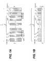
- FIGS. 1A and 1Billustrate a pattern in a semiconductor device according to an embodiment of the invention.
- FIGS. 2A to 2Fare sectional views illustrating a method of manufacturing a semiconductor device according to the embodiment.
- a semiconductor device manufacturing methodwill be described with reference to FIGS. 1A and 1B and FIGS. 2A to 2F . Forming of gate patterns of a NAND flash memory by the semiconductor device manufacturing method will be described here.
- FIGS. 1A and 1Billustrate gate patterns of an NAND flash memory.
- FIG. 1Ashows a plan view of the gate patterns.
- FIG. 1Bshows a sectional view of the gate patterns taken along the broken line A-A′ in FIG. 1A .
- the gate patterns 1include: line-and-space-shaped patterns 2 (line-and-space patterns 2 ) having a number X of parallel line patterns (L 1 to LX) arranged periodically with given spaces; and aperiodic patterns 3 disposed aperiodically adjacent to opposite end portions of the line-and-space patterns 2 .
- the line-and-space patterns 2are functioning as word lines, and the periodic patterns 3 are functioning as select gate patterns SG 1 and SG 2 .
- the select gate patternsare aperiodic” means that the select gate patterns are aperiodic relative to the line-and-space patterns 2 . Accordingly, the select gate patterns may be periodic to each other or may be periodic relative to other patterns (except dummy patterns which will be described later) than the line-and-space patterns 2 .
- the line sizes (W 1 to WX) and the space sizes (S 1 to SX)are equal to one another.
- the line size, the space size and the number of linescan be set respectively arbitrarily.
- the line size and the space sizecan be set to be in a range of from about 30 nm to about 60 nm and the number of lines can be set to be 16, 32, 64 or 128.
- extracted patterns on which contacts with upper layer wiring are to be disposedare connected to the line patterns of the line-and-space patterns 2 respectively.
- the distance between each select gate pattern SG 1 or SG 2 and the line-and-space patterns 2is larger than the line size and space size of the line-and-space patterns 2 .
- the distance between each select gate pattern SG 1 or SG 2 and the line-and-space patterns 2can be set to be about three times as much as the line size and space size.
- a dummy pattern 4is provided between the line-and-space periodic patterns 2 and each aperiodic pattern 3 .
- the dummy patterns 4are formed so as to be electrically independent of the periodic patterns 2 and the aperiodic patterns 3 .
- the dummy patterns 4are line-shaped patterns parallel with the respective line patterns of the line-and-space patterns 2 .
- the dummy patterns 4are formed adjacent to the line-and-space patterns 2 .
- Each dummy pattern 4is formed distant from a corresponding end line pattern (L 1 , LX) of the line-and-space patterns 2 by the same size (SO, SX+1) as the space size (S 1 to SX) of the line-and-space patterns 2 .
- each end line pattern (L 1 , LX) of the line-and-space patterns 2 and a pattern adjacent to the end line pattern (L 1 , LX)is equalized to the distance between the central line pattern (LX/ 2 ) of the line-and-space patterns 2 and a pattern adjacent to the central line pattern (LX/ 2 ), so that the same peripheral environment is provided in each line pattern.
- each dummy pattern 4is equal to the size of each line pattern (L 1 to LX) of the line-and-space patterns 2 . Accordingly, the size of each end line pattern (L 1 , LX) of the line-and-space patterns 2 and the size of the central line pattern (LX/ 2 ) of the line-and-space patterns 2 are equalized to the size of a pattern adjacent to the end line pattern (L 1 , LX) and the size of a pattern adjacent to the central line pattern (LX/ 2 ), so that the same peripheral environment is provided in each line pattern.
- the line-and-space patterns 2 , the select gate patterns (aperiodic patterns 3 ) and the dummy patterns 4are formed on a semiconductor substrate 5 through a gate insulating film (not shown) and made of polysilicon materials respectively.
- FIGS. 2A to 2Fare sectional views illustrating the method of forming the gate patterns 1 of the semiconductor device shown in FIG. 1B .
- a target film 6 of a gate pattern material such as a polysilicon filmis formed on a semiconductor substrate 5 through a gate insulating film (not shown). Then, a first film 7 of a laminated structure having a silicon oxide film 7 a and an amorphous silicon film 7 b is formed on the target film 6 . A resist film is formed on the first film 7 through an antireflection film (not shown) in a coating manner. Then, after a photo mask is disposed in an exposure device, a mask pattern image is formed in the resist film by the exposure device. The resist film is developed to form resist patterns 8 .
- a gate pattern materialsuch as a polysilicon film
- the resist patterns 8include: line-and-space patterns 9 having a number (1+X/ 2 ) of parallel line patterns arranged periodically with given spaces; and aperiodic patterns 10 disposed adjacent to the line-and-space patterns.
- the amorphous silicon film 7 b masked with the resist patterns 8is processed. Then, the resist patterns 8 are removed, and the amorphous silicon film 7 b is subjected to slimming in an etching manner. Then, the silicon oxide film 7 a masked with the slimmed amorphous silicon film 7 b is processed.
- first patterns 11 formed in the first film 7include: line-and-space patterns 12 having a number (1+X/ 2 ) of parallel line patterns arranged periodically; and aperiodic patterns 13 disposed adjacent to the line-and-space patterns.
- the line-and-space patterns 12are formed so that the ratio of the line size to the space size is 1:3.
- a laminated film having a silicon oxide film 7 a and an amorphous silicon film 7 bis used as the first film 7 formed on the target film 6 .
- a laminated film formed of other materialssuch as a laminated film having a carbon film and an amorphous silicon film, a laminated film having a carbon film and an SOG film or a single layer film such as a silicon nitride film may be used as the first film 7 .
- the amorphous silicon film 7 b as an upper layer portion of the first film 7is subjected to slimming.
- the amorphous silicon film 7 b masked with the resist patterns 8may be processed after the resist patterns 8 are subjected to slimming. In this case, the step of applying slimming to the amorphous silicon film 7 b can be removed.
- a second film 14such as an oxide film, a nitride film, etc. is formed on the target film 6 and on the first patterns 11 so that the first patterns 11 are covered with the second film 14 .
- the second film 14is etched to form second side wall patterns 15 on side walls of the first patterns 11 .
- periodically arranged patterns 12are selectively removed from the first patterns 11 . That is, a resist film is applied on the target film 6 , the first patterns 11 and the second side wall patterns 15 , the resist film is processed to have patterns selectively revealing the periodically arranged patterns 12 of the first patterns 11 and the second side wall patterns 15 formed on side walls thereof, and the revealed periodic patterns 12 are removed with the resist patterns.
- the second side wall patterns 15are formed as line-and-space patterns 16 having a number (X+2) of line patterns parallel with one another and periodically arranged.
- the line-and-space patterns 16are formed so that the ratio of the line size to the space size is 1:1.
- the target film 6 masked with the first patterns 11 and the second side wall pattern 15is processed to form gate patterns 1 as shown in FIG. 1B .
- line-and-space patterns 2as word lines, having a number X of line patterns arranged periodically and each separated from the adjacent line patterns, aperiodic select gate patterns 3 arranged adjacent to the line-and-space patterns, and electrically-independent dummy patterns 4 formed between the line-and-space patterns 2 and the select gate patterns 3 are simultaneously formed on the semiconductor substrate 5 as shown in FIG. 1B .
- the dummy patterns 4 and the line-and-space patterns 2 formed in the target film 6are formed simultaneously with the second side wall patterns 15 of periodic line-and-space patterns as a mask.
- the dummy patterns 4are provided as two line patterns respectively adjacent to end line patterns of the line-and-space patterns 2 to be periodic with respect to the line-and-space patterns 2 .
- the distance (space size) between each end line of the line-and-space patterns 2 and a pattern adjacent to the end line and the distance (space size) between the central line of the line-and-space patterns 2 and a pattern adjacent to the central lineare equalized. Further, the size of a pattern adjacent to the end line of the line-and-space patterns 2 and the size of a pattern adjacent to the central line of the line-and-space patterns 2 are equalized.
- each end line of the periodic line-and-space patterns 2 and the central line of the periodic line-and-space patterns 2have the same peripheral pattern environment. Accordingly, dimensional error caused in an etching process or the like can be suppressed.
- the dummy patterns 4are formed by use of the second side wall patterns 15 that are used to form fine-size target patterns in the target film 6 .
- the dummy patterns 4can be formed while preventing the chip area from being increased.
- two resist dummy regionsare provided between periodic patterns and aperiodic patterns. For example, if two resist patterns are provided correspondingly for the two dummy regions, since two side-wall patterns are formed at both sides of one resist pattern, two dummy patterns are formed in each of the two dummy regions.
- gate patterns of an NAND flash memoryis described.
- the inventioncan be applied to formation of other patterns of semiconductor device.
- this embodimentis applied to a method of manufacturing a semiconductor device having periodic patterns and aperiodic patterns, dummy patterns can be formed therebetween.
Landscapes
- Engineering & Computer Science (AREA)
- Microelectronics & Electronic Packaging (AREA)
- Condensed Matter Physics & Semiconductors (AREA)
- General Physics & Mathematics (AREA)
- Manufacturing & Machinery (AREA)
- Computer Hardware Design (AREA)
- Physics & Mathematics (AREA)
- Power Engineering (AREA)
- Chemical & Material Sciences (AREA)
- Inorganic Chemistry (AREA)
- Semiconductor Memories (AREA)
- Non-Volatile Memory (AREA)
- Internal Circuitry In Semiconductor Integrated Circuit Devices (AREA)
Abstract
Description
- This application claims priority from Japanese Patent Application No. 2008-255638 filed on Sep. 30, 2008, the entire contents of which are incorporated herein by reference.
- 1. Field of the Invention
- An aspect of the present invention relates to a method of manufacturing a semiconductor device.
- 2. Description of the Related Art
- As a technique for achieving a fine structure of wiring patterns or the like in a semiconductor integrated circuit or the like, there is proposed a pattern forming method in which side wall patterns are formed on side walls of core patterns formed on a target film and in which the target film masked with the side wall patterns or patterns embedded in between the side wall patterns are processed to form wiring patterns, gate electrodes, etc. (e.g. see U.S. Pat. No. 6,063,688). By such method, for example, line-and-space-shaped periodic patterns can be formed.
- In the periodic patterns such as line-and-space patterns, even when end patterns and a central pattern are designed to be equal, each end pattern and the central pattern are different in arrangement environment. Accordingly, each end pattern and the central pattern are different in the influence of a proximity effect caused in a manufacturing process, and there is a possibility that dimensional error may occur.
- According to an aspect of the present invention, there is provided a method of manufacturing a semiconductor device, the method including: forming a first film on a target film; forming resist patterns on the first film; processing the first film with the resist patterns as a mask, thereby forming first patterns including: periodic patterns arranged periodically; and aperiodic patterns arranged aperiodically with respect to the periodic patterns; removing the resist patterns; forming a second film on the target film to cover the first patterns; processing the second film to reveal the target film, thereby forming second side wall patterns on side walls of the first patterns; selectively removing the periodic patterns of the first patterns to leave the aperiodic patterns of the first patterns; and processing the target film with the aperiodic patterns of the first patterns and the second side wall patterns as a mask, thereby forming a target patterns including: periodic target patterns arranged periodically; aperiodic target patterns arranged adjacent to both end parts of the periodic target patterns and arranged aperiodically with respect to the periodic target patterns; and dummy patterns arranged between the periodic target patterns and the aperiodic patterns and arranged periodically with respect to the periodic target patterns.
- Another aspect of the present invention, there is provided a memory device including: a semiconductor substrate; a insulating film formed on the semiconductor substrate; a plurality of word lines arranged periodically; two of select gates arranged at both ends of the word lines, each select gate being arranged aperiodically with respect to the word lines; and two of dummy patterns arranged between the word lines and each select gate, each dummy pattern being arranged periodically with respect to the word lines.
FIGS. 1A and 1B illustrate a pattern in a semiconductor device according to an embodiment of the invention.FIGS. 2A to 2F are sectional views illustrating a method of manufacturing a semiconductor device according to the embodiment.- An embodiment of the invention will be described below in detail with reference to the drawings.
- A semiconductor device manufacturing method according to this embodiment will be described with reference to
FIGS. 1A and 1B andFIGS. 2A to 2F . Forming of gate patterns of a NAND flash memory by the semiconductor device manufacturing method will be described here. FIGS. 1A and 1B illustrate gate patterns of an NAND flash memory.FIG. 1A shows a plan view of the gate patterns.FIG. 1B shows a sectional view of the gate patterns taken along the broken line A-A′ inFIG. 1A .- As shown in
FIG. 1A , thegate patterns 1 include: line-and-space-shaped patterns2 (line-and-space patterns2) having a number X of parallel line patterns (L1 to LX) arranged periodically with given spaces; andaperiodic patterns 3 disposed aperiodically adjacent to opposite end portions of the line-and-space patterns 2. The line-and-space patterns 2 are functioning as word lines, and theperiodic patterns 3 are functioning as select gate patterns SG1 and SG2. - The fact that “the select gate patterns are aperiodic” means that the select gate patterns are aperiodic relative to the line-and-
space patterns 2. Accordingly, the select gate patterns may be periodic to each other or may be periodic relative to other patterns (except dummy patterns which will be described later) than the line-and-space patterns 2. - In this embodiment, in the line-and-
space patterns 2, the line sizes (W1 to WX) and the space sizes (S1 to SX) are equal to one another. The line size, the space size and the number of lines can be set respectively arbitrarily. For example, the line size and the space size can be set to be in a range of from about 30 nm to about 60 nm and the number of lines can be set to be 16, 32, 64 or 128. Though not shown, extracted patterns on which contacts with upper layer wiring are to be disposed are connected to the line patterns of the line-and-space patterns 2 respectively. - The distance between each select gate pattern SG1 or SG2 and the line-and-
space patterns 2 is larger than the line size and space size of the line-and-space patterns 2. For example, the distance between each select gate pattern SG1 or SG2 and the line-and-space patterns 2 can be set to be about three times as much as the line size and space size. - In this embodiment, a
dummy pattern 4 is provided between the line-and-spaceperiodic patterns 2 and eachaperiodic pattern 3. Thedummy patterns 4 are formed so as to be electrically independent of theperiodic patterns 2 and theaperiodic patterns 3. - The
dummy patterns 4 are line-shaped patterns parallel with the respective line patterns of the line-and-space patterns 2. Thedummy patterns 4 are formed adjacent to the line-and-space patterns 2. Eachdummy pattern 4 is formed distant from a corresponding end line pattern (L1, LX) of the line-and-space patterns 2 by the same size (SO, SX+1) as the space size (S1 to SX) of the line-and-space patterns 2. Accordingly, the distance between each end line pattern (L1, LX) of the line-and-space patterns 2 and a pattern adjacent to the end line pattern (L1, LX) is equalized to the distance between the central line pattern (LX/2) of the line-and-space patterns 2 and a pattern adjacent to the central line pattern (LX/2), so that the same peripheral environment is provided in each line pattern. - The size of each
dummy pattern 4 is equal to the size of each line pattern (L1 to LX) of the line-and-space patterns 2. Accordingly, the size of each end line pattern (L1, LX) of the line-and-space patterns 2 and the size of the central line pattern (LX/2) of the line-and-space patterns 2 are equalized to the size of a pattern adjacent to the end line pattern (L1, LX) and the size of a pattern adjacent to the central line pattern (LX/2), so that the same peripheral environment is provided in each line pattern. - As shown in
FIG. 1B , the line-and-space patterns 2, the select gate patterns (aperiodic patterns3) and thedummy patterns 4 are formed on asemiconductor substrate 5 through a gate insulating film (not shown) and made of polysilicon materials respectively. - A method of forming the
gate patterns 1 of the semiconductor device shown inFIGS. 1A and 1B will be described below with reference toFIGS. 2A to 2F .FIGS. 2A to 2F are sectional views illustrating the method of forming thegate patterns 1 of the semiconductor device shown inFIG. 1B . - First, as shown in
FIG. 2A , atarget film 6 of a gate pattern material such as a polysilicon film is formed on asemiconductor substrate 5 through a gate insulating film (not shown). Then, a first film7 of a laminated structure having asilicon oxide film 7aand an amorphous silicon film7bis formed on thetarget film 6. A resist film is formed on the first film7 through an antireflection film (not shown) in a coating manner. Then, after a photo mask is disposed in an exposure device, a mask pattern image is formed in the resist film by the exposure device. The resist film is developed to form resist patterns8. - The resist patterns8 include: line-and-space patterns9 having a number (1+X/2) of parallel line patterns arranged periodically with given spaces; and
aperiodic patterns 10 disposed adjacent to the line-and-space patterns. - Then, as shown in
FIG. 2B , the amorphous silicon film7bmasked with the resist patterns8 is processed. Then, the resist patterns8 are removed, and the amorphous silicon film7bis subjected to slimming in an etching manner. Then, thesilicon oxide film 7amasked with the slimmed amorphous silicon film7bis processed. - Like the resist patterns8, first patterns11 formed in the first film7 include: line-and-
space patterns 12 having a number (1+X/2) of parallel line patterns arranged periodically; andaperiodic patterns 13 disposed adjacent to the line-and-space patterns. The line-and-space patterns 12 are formed so that the ratio of the line size to the space size is 1:3. - In this embodiment, as the first film7 formed on the
target film 6, a laminated film having asilicon oxide film 7aand an amorphous silicon film7bis used. However, a laminated film formed of other materials such as a laminated film having a carbon film and an amorphous silicon film, a laminated film having a carbon film and an SOG film or a single layer film such as a silicon nitride film may be used as the first film7. - In this embodiment, the amorphous silicon film7bas an upper layer portion of the first film7 is subjected to slimming. However, the amorphous silicon film7bmasked with the resist patterns8 may be processed after the resist patterns8 are subjected to slimming. In this case, the step of applying slimming to the amorphous silicon film7bcan be removed.
- Then, as shown in
FIG. 2C , asecond film 14 such as an oxide film, a nitride film, etc. is formed on thetarget film 6 and on the first patterns11 so that the first patterns11 are covered with thesecond film 14. - Then, as shown in
FIG. 2D , thesecond film 14 is etched to form secondside wall patterns 15 on side walls of the first patterns11. - Then, as shown in
FIG. 2E , periodically arrangedpatterns 12 are selectively removed from the first patterns11. That is, a resist film is applied on thetarget film 6, the first patterns11 and the secondside wall patterns 15, the resist film is processed to have patterns selectively revealing the periodically arrangedpatterns 12 of the first patterns11 and the secondside wall patterns 15 formed on side walls thereof, and the revealedperiodic patterns 12 are removed with the resist patterns. - As a result of selectively removing the first patterns11, the second
side wall patterns 15 are formed as line-and-space patterns 16 having a number (X+2) of line patterns parallel with one another and periodically arranged. The line-and-space patterns 16 are formed so that the ratio of the line size to the space size is 1:1. - Finally, as shown in
FIG. 2F , thetarget film 6 masked with the first patterns11 and the secondside wall pattern 15 is processed to formgate patterns 1 as shown inFIG. 1B . - In this manner, line-and-
space patterns 2, as word lines, having a number X of line patterns arranged periodically and each separated from the adjacent line patterns, aperiodicselect gate patterns 3 arranged adjacent to the line-and-space patterns, and electrically-independent dummy patterns 4 formed between the line-and-space patterns 2 and theselect gate patterns 3 are simultaneously formed on thesemiconductor substrate 5 as shown inFIG. 1B . - The
dummy patterns 4 and the line-and-space patterns 2 formed in thetarget film 6 are formed simultaneously with the secondside wall patterns 15 of periodic line-and-space patterns as a mask. Thedummy patterns 4 are provided as two line patterns respectively adjacent to end line patterns of the line-and-space patterns 2 to be periodic with respect to the line-and-space patterns 2. - For this reason, the distance (space size) between each end line of the line-and-
space patterns 2 and a pattern adjacent to the end line and the distance (space size) between the central line of the line-and-space patterns 2 and a pattern adjacent to the central line are equalized. Further, the size of a pattern adjacent to the end line of the line-and-space patterns 2 and the size of a pattern adjacent to the central line of the line-and-space patterns 2 are equalized. - According to this embodiment, each end line of the periodic line-and-
space patterns 2 and the central line of the periodic line-and-space patterns 2 have the same peripheral pattern environment. Accordingly, dimensional error caused in an etching process or the like can be suppressed. - In this embodiment, the
dummy patterns 4 are formed by use of the secondside wall patterns 15 that are used to form fine-size target patterns in thetarget film 6. As a result, thedummy patterns 4 can be formed while preventing the chip area from being increased. - Generally, in the semiconductor device, two resist dummy regions are provided between periodic patterns and aperiodic patterns. For example, if two resist patterns are provided correspondingly for the two dummy regions, since two side-wall patterns are formed at both sides of one resist pattern, two dummy patterns are formed in each of the two dummy regions.
- In this embodiment, only one resist pattern in total is formed to provide the two dummy regions, and the one
dummy pattern 4 is respectively assigned between theperiodic patterns 2 and eachaperiodic pattern 3. Therefore, the area required for providing the dummy regions are reduced as compared with the above comparison example. - According to this embodiment, while suppressing dimensional error of patterns, pattern area in the lithography is prevented so that chip area of the semiconductor device is suppressed.
- In this embodiment, formation of gate patterns of an NAND flash memory is described. However, the invention can be applied to formation of other patterns of semiconductor device. For example, when this embodiment is applied to a method of manufacturing a semiconductor device having periodic patterns and aperiodic patterns, dummy patterns can be formed therebetween.
Claims (12)
Applications Claiming Priority (2)
| Application Number | Priority Date | Filing Date | Title |
|---|---|---|---|
| JP2008255638AJP2010087301A (en) | 2008-09-30 | 2008-09-30 | Method for manufacturing semiconductor device |
| JPP2008-255638 | 2008-09-30 |
Publications (2)
| Publication Number | Publication Date |
|---|---|
| US20100081265A1true US20100081265A1 (en) | 2010-04-01 |
| US7713833B2 US7713833B2 (en) | 2010-05-11 |
Family
ID=42057908
Family Applications (1)
| Application Number | Title | Priority Date | Filing Date |
|---|---|---|---|
| US12/557,111ActiveUS7713833B2 (en) | 2008-09-30 | 2009-09-10 | Method for manufacturing semiconductor device |
Country Status (2)
| Country | Link |
|---|---|
| US (1) | US7713833B2 (en) |
| JP (1) | JP2010087301A (en) |
Cited By (13)
| Publication number | Priority date | Publication date | Assignee | Title |
|---|---|---|---|---|
| US20080008969A1 (en)* | 2006-07-10 | 2008-01-10 | Micron Technology, Inc. | Pitch reduction technology using alternating spacer depositions during the formation of a semiconductor device and systems including same |
| US20100144153A1 (en)* | 2008-12-04 | 2010-06-10 | Scott Sills | Methods of Fabricating Substrates |
| US20100144150A1 (en)* | 2008-12-04 | 2010-06-10 | Micron Technology, Inc. | Methods of Fabricating Substrates |
| US20100144151A1 (en)* | 2008-12-04 | 2010-06-10 | Scott Sills | Methods of Fabricating Substrates |
| US20100291771A1 (en)* | 2009-05-18 | 2010-11-18 | Baosuo Zhou | Methods Of Forming Patterns On Substrates |
| US20120058633A1 (en)* | 2010-09-02 | 2012-03-08 | Russell Stephen W | Methods Of Forming Features Of Integrated Circuitry |
| US8563228B2 (en) | 2009-03-23 | 2013-10-22 | Micron Technology, Inc. | Methods of forming patterns on substrates |
| US8575032B2 (en) | 2011-05-05 | 2013-11-05 | Micron Technology, Inc. | Methods of forming a pattern on a substrate |
| US8629048B1 (en) | 2012-07-06 | 2014-01-14 | Micron Technology, Inc. | Methods of forming a pattern on a substrate |
| US8629527B2 (en) | 2008-05-05 | 2014-01-14 | Micron Technology, Inc. | Semiconductor structures |
| US8994088B2 (en) | 2012-09-10 | 2015-03-31 | Kabushiki Kaisha Toshiba | Semiconductor storage device and manufacturing method thereof |
| US9177794B2 (en) | 2012-01-13 | 2015-11-03 | Micron Technology, Inc. | Methods of patterning substrates |
| US10151981B2 (en) | 2008-05-22 | 2018-12-11 | Micron Technology, Inc. | Methods of forming structures supported by semiconductor substrates |
Families Citing this family (3)
| Publication number | Priority date | Publication date | Assignee | Title |
|---|---|---|---|---|
| JP5361790B2 (en)* | 2010-04-28 | 2013-12-04 | 株式会社東芝 | Method for surface treatment of semiconductor substrate |
| JP5389075B2 (en)* | 2011-03-03 | 2014-01-15 | 株式会社東芝 | Method for manufacturing nonvolatile semiconductor memory device |
| JP5395837B2 (en) | 2011-03-24 | 2014-01-22 | 株式会社東芝 | Manufacturing method of semiconductor device |
Citations (4)
| Publication number | Priority date | Publication date | Assignee | Title |
|---|---|---|---|---|
| US20070196986A1 (en)* | 2006-02-21 | 2007-08-23 | Masayuki Ichige | Method for manufacturing semiconductor device |
| US20080014510A1 (en)* | 2006-07-13 | 2008-01-17 | Kabushiki Kaisha Toshiba | Photomask designing apparatus, photomask, photomask designing method, photomask designing program and computer-readable storage medium on which the photomask designing program is stored |
| US20080303115A1 (en)* | 2007-06-06 | 2008-12-11 | Kabushiki Kaisha Toshiba | Semiconductor memory device and method of fabricating the same |
| US20090039519A1 (en)* | 2007-08-10 | 2009-02-12 | Renesas Technology Corp. | Semiconductor device, photomask, semiconductor device production method, and pattern layout method |
Family Cites Families (7)
| Publication number | Priority date | Publication date | Assignee | Title |
|---|---|---|---|---|
| US6063688A (en) | 1997-09-29 | 2000-05-16 | Intel Corporation | Fabrication of deep submicron structures and quantum wire transistors using hard-mask transistor width definition |
| JP4005895B2 (en)* | 2002-09-30 | 2007-11-14 | 株式会社東芝 | Nonvolatile semiconductor memory device |
| US20050009312A1 (en)* | 2003-06-26 | 2005-01-13 | International Business Machines Corporation | Gate length proximity corrected device |
| JP4634849B2 (en)* | 2005-04-12 | 2011-02-16 | 株式会社東芝 | Integrated circuit pattern layout, photomask, semiconductor device manufacturing method, and data creation method |
| JP4921723B2 (en)* | 2005-04-18 | 2012-04-25 | 株式会社東芝 | Manufacturing method of semiconductor device |
| US8158333B2 (en) | 2006-04-11 | 2012-04-17 | Kabushiki Kaisha Toshiba | Manufacturing method of semiconductor device |
| US7808053B2 (en) | 2006-12-29 | 2010-10-05 | Intel Corporation | Method, apparatus, and system for flash memory |
- 2008
- 2008-09-30JPJP2008255638Apatent/JP2010087301A/enactivePending
- 2009
- 2009-09-10USUS12/557,111patent/US7713833B2/enactiveActive
Patent Citations (4)
| Publication number | Priority date | Publication date | Assignee | Title |
|---|---|---|---|---|
| US20070196986A1 (en)* | 2006-02-21 | 2007-08-23 | Masayuki Ichige | Method for manufacturing semiconductor device |
| US20080014510A1 (en)* | 2006-07-13 | 2008-01-17 | Kabushiki Kaisha Toshiba | Photomask designing apparatus, photomask, photomask designing method, photomask designing program and computer-readable storage medium on which the photomask designing program is stored |
| US20080303115A1 (en)* | 2007-06-06 | 2008-12-11 | Kabushiki Kaisha Toshiba | Semiconductor memory device and method of fabricating the same |
| US20090039519A1 (en)* | 2007-08-10 | 2009-02-12 | Renesas Technology Corp. | Semiconductor device, photomask, semiconductor device production method, and pattern layout method |
Cited By (31)
| Publication number | Priority date | Publication date | Assignee | Title |
|---|---|---|---|---|
| US11935756B2 (en) | 2006-07-10 | 2024-03-19 | Lodestar Licensing Group Llc | Pitch reduction technology using alternating spacer depositions during the formation of a semiconductor device and systems including same |
| US11335563B2 (en) | 2006-07-10 | 2022-05-17 | Micron Technology, Inc. | Pitch reduction technology using alternating spacer depositions during the formation of a semiconductor device and systems including same |
| US10607844B2 (en) | 2006-07-10 | 2020-03-31 | Micron Technology, Inc. | Pitch reduction technology using alternating spacer depositions during the formation of a semiconductor device and systems including same |
| US10096483B2 (en) | 2006-07-10 | 2018-10-09 | Micron Technology, Inc. | Pitch reduction technology using alternating spacer depositions during the formation of a semiconductor device and systems including same |
| US9761457B2 (en) | 2006-07-10 | 2017-09-12 | Micron Technology, Inc. | Pitch reduction technology using alternating spacer depositions during the formation of a semiconductor device and systems including same |
| US9305782B2 (en) | 2006-07-10 | 2016-04-05 | Micron Technology, Inc. | Pitch reduction technology using alternating spacer depositions during the formation of a semiconductor device and systems including same |
| US8852851B2 (en) | 2006-07-10 | 2014-10-07 | Micron Technology, Inc. | Pitch reduction technology using alternating spacer depositions during the formation of a semiconductor device and systems including same |
| US20080008969A1 (en)* | 2006-07-10 | 2008-01-10 | Micron Technology, Inc. | Pitch reduction technology using alternating spacer depositions during the formation of a semiconductor device and systems including same |
| US8629527B2 (en) | 2008-05-05 | 2014-01-14 | Micron Technology, Inc. | Semiconductor structures |
| US8901700B2 (en) | 2008-05-05 | 2014-12-02 | Micron Technology, Inc. | Semiconductor structures |
| US10151981B2 (en) | 2008-05-22 | 2018-12-11 | Micron Technology, Inc. | Methods of forming structures supported by semiconductor substrates |
| US8703570B2 (en) | 2008-12-04 | 2014-04-22 | Micron Technology, Inc. | Methods of fabricating substrates |
| US8603884B2 (en) | 2008-12-04 | 2013-12-10 | Micron Technology, Inc. | Methods of fabricating substrates |
| US20100144153A1 (en)* | 2008-12-04 | 2010-06-10 | Scott Sills | Methods of Fabricating Substrates |
| US8796155B2 (en) | 2008-12-04 | 2014-08-05 | Micron Technology, Inc. | Methods of fabricating substrates |
| US20100144150A1 (en)* | 2008-12-04 | 2010-06-10 | Micron Technology, Inc. | Methods of Fabricating Substrates |
| US8247302B2 (en) | 2008-12-04 | 2012-08-21 | Micron Technology, Inc. | Methods of fabricating substrates |
| US20100144151A1 (en)* | 2008-12-04 | 2010-06-10 | Scott Sills | Methods of Fabricating Substrates |
| US9653315B2 (en) | 2008-12-04 | 2017-05-16 | Micron Technology, Inc. | Methods of fabricating substrates |
| US8273634B2 (en) | 2008-12-04 | 2012-09-25 | Micron Technology, Inc. | Methods of fabricating substrates |
| US8563228B2 (en) | 2009-03-23 | 2013-10-22 | Micron Technology, Inc. | Methods of forming patterns on substrates |
| US9330934B2 (en) | 2009-05-18 | 2016-05-03 | Micron Technology, Inc. | Methods of forming patterns on substrates |
| US20100291771A1 (en)* | 2009-05-18 | 2010-11-18 | Baosuo Zhou | Methods Of Forming Patterns On Substrates |
| US8455341B2 (en)* | 2010-09-02 | 2013-06-04 | Micron Technology, Inc. | Methods of forming features of integrated circuitry |
| US20120058633A1 (en)* | 2010-09-02 | 2012-03-08 | Russell Stephen W | Methods Of Forming Features Of Integrated Circuitry |
| US9153458B2 (en) | 2011-05-05 | 2015-10-06 | Micron Technology, Inc. | Methods of forming a pattern on a substrate |
| US8575032B2 (en) | 2011-05-05 | 2013-11-05 | Micron Technology, Inc. | Methods of forming a pattern on a substrate |
| US9177794B2 (en) | 2012-01-13 | 2015-11-03 | Micron Technology, Inc. | Methods of patterning substrates |
| US8629048B1 (en) | 2012-07-06 | 2014-01-14 | Micron Technology, Inc. | Methods of forming a pattern on a substrate |
| US8846517B2 (en) | 2012-07-06 | 2014-09-30 | Micron Technology, Inc. | Methods of forming a pattern on a substrate |
| US8994088B2 (en) | 2012-09-10 | 2015-03-31 | Kabushiki Kaisha Toshiba | Semiconductor storage device and manufacturing method thereof |
Also Published As
| Publication number | Publication date |
|---|---|
| JP2010087301A (en) | 2010-04-15 |
| US7713833B2 (en) | 2010-05-11 |
Similar Documents
| Publication | Publication Date | Title |
|---|---|---|
| US7713833B2 (en) | Method for manufacturing semiconductor device | |
| US7604926B2 (en) | Method of manufacturing a semiconductor device | |
| US8759224B2 (en) | Method of forming a pattern structure for a semiconductor device | |
| KR101149632B1 (en) | Semiconductor constructions, methods of forming multiple lines, and methods of forming high density structures and low density structures with a single photomask | |
| US8110340B2 (en) | Method of forming a pattern of a semiconductor device | |
| US8343874B2 (en) | Semiconductor device manufacturing method | |
| US8298953B2 (en) | Method for defining a separating structure within a semiconductor device | |
| US8969199B1 (en) | Methods of forming a circuit that includes a cross-coupling gate contact structure wherein the circuit is to be manufactured using a triple patterning process | |
| CN101542390A (en) | Double patterning for lithography to increase feature spatial density | |
| KR20090042458A (en) | Pattern formation method of semiconductor memory device using spacer | |
| KR20090023825A (en) | Method of forming fine pattern of semiconductor device | |
| KR20110001189A (en) | Method for forming semiconductor device | |
| US7910289B2 (en) | Use of dual mask processing of different composition such as inorganic/organic to enable a single poly etch using a two-print-two-etch approach | |
| KR20080030237A (en) | Metal wiring of semiconductor device | |
| US8088689B2 (en) | Method of fabricating semiconductor device | |
| JP2007150166A (en) | Manufacturing method of semiconductor device | |
| US20210351036A1 (en) | Semiconductor patterning process | |
| US10056257B2 (en) | Methods for forming fine patterns using spacers | |
| US10290543B1 (en) | Method for manufacturing semiconductor device | |
| KR100940275B1 (en) | Gate pattern formation method of semiconductor device | |
| US7473631B2 (en) | Method of forming contact holes in a semiconductor device having first and second metal layers | |
| CN111106001A (en) | Method for forming gate structure of NAND memory, NAND memory and photomask mask | |
| US20050230738A1 (en) | NAND type flash memory device, and method for manufacturing the same | |
| JP2002319584A (en) | Method for manufacturing semiconductor device | |
| US8057987B2 (en) | Patterning method of semiconductor device |
Legal Events
| Date | Code | Title | Description |
|---|---|---|---|
| AS | Assignment | Owner name:KABUSHIKI KAISHA TOSHIBA,JAPAN Free format text:ASSIGNMENT OF ASSIGNORS INTEREST;ASSIGNORS:MASHITA, HIROMITSU;KOTANI, TOSHIYA;MUKAI, HIDEFUMI;AND OTHERS;REEL/FRAME:023217/0074 Effective date:20090827 | |
| STCF | Information on status: patent grant | Free format text:PATENTED CASE | |
| CC | Certificate of correction | ||
| FEPP | Fee payment procedure | Free format text:PAYOR NUMBER ASSIGNED (ORIGINAL EVENT CODE: ASPN); ENTITY STATUS OF PATENT OWNER: LARGE ENTITY | |
| FPAY | Fee payment | Year of fee payment:4 | |
| AS | Assignment | Owner name:TOSHIBA MEMORY CORPORATION, JAPAN Free format text:ASSIGNMENT OF ASSIGNORS INTEREST;ASSIGNOR:KABUSHIKI KAISHA TOSHIBA;REEL/FRAME:043709/0035 Effective date:20170706 | |
| MAFP | Maintenance fee payment | Free format text:PAYMENT OF MAINTENANCE FEE, 8TH YEAR, LARGE ENTITY (ORIGINAL EVENT CODE: M1552) Year of fee payment:8 | |
| AS | Assignment | Owner name:K.K. PANGEA, JAPAN Free format text:MERGER;ASSIGNOR:TOSHIBA MEMORY CORPORATION;REEL/FRAME:055659/0471 Effective date:20180801 Owner name:TOSHIBA MEMORY CORPORATION, JAPAN Free format text:CHANGE OF NAME AND ADDRESS;ASSIGNOR:K.K. PANGEA;REEL/FRAME:055669/0401 Effective date:20180801 Owner name:KIOXIA CORPORATION, JAPAN Free format text:CHANGE OF NAME AND ADDRESS;ASSIGNOR:TOSHIBA MEMORY CORPORATION;REEL/FRAME:055669/0001 Effective date:20191001 | |
| MAFP | Maintenance fee payment | Free format text:PAYMENT OF MAINTENANCE FEE, 12TH YEAR, LARGE ENTITY (ORIGINAL EVENT CODE: M1553); ENTITY STATUS OF PATENT OWNER: LARGE ENTITY Year of fee payment:12 |