US20100079632A1 - Correlated double sampling pixel - Google Patents
Correlated double sampling pixelDownload PDFInfo
- Publication number
- US20100079632A1 US20100079632A1US12/284,901US28490108AUS2010079632A1US 20100079632 A1US20100079632 A1US 20100079632A1US 28490108 AUS28490108 AUS 28490108AUS 2010079632 A1US2010079632 A1US 2010079632A1
- Authority
- US
- United States
- Prior art keywords
- capacitor
- voltage value
- coupled
- reset
- sensor circuit
- Prior art date
- Legal status (The legal status is an assumption and is not a legal conclusion. Google has not performed a legal analysis and makes no representation as to the accuracy of the status listed.)
- Granted
Links
Images


Classifications
- H—ELECTRICITY
- H04—ELECTRIC COMMUNICATION TECHNIQUE
- H04N—PICTORIAL COMMUNICATION, e.g. TELEVISION
- H04N25/00—Circuitry of solid-state image sensors [SSIS]; Control thereof
- H04N25/60—Noise processing, e.g. detecting, correcting, reducing or removing noise
- H04N25/616—Noise processing, e.g. detecting, correcting, reducing or removing noise involving a correlated sampling function, e.g. correlated double sampling [CDS] or triple sampling
- H—ELECTRICITY
- H04—ELECTRIC COMMUNICATION TECHNIQUE
- H04N—PICTORIAL COMMUNICATION, e.g. TELEVISION
- H04N25/00—Circuitry of solid-state image sensors [SSIS]; Control thereof
- H04N25/70—SSIS architectures; Circuits associated therewith
- H04N25/76—Addressed sensors, e.g. MOS or CMOS sensors
- H04N25/77—Pixel circuitry, e.g. memories, A/D converters, pixel amplifiers, shared circuits or shared components
- H04N25/771—Pixel circuitry, e.g. memories, A/D converters, pixel amplifiers, shared circuits or shared components comprising storage means other than floating diffusion
Definitions
- the present disclosurerelates generally to image sensors and more particularly to a correlated double sampling pixel and methods of operating the same.
- a design criterion in image sensorsincludes dynamic range, which is defined as a logarithmic ratio between the full scale voltage swing on the photodetector and the smallest detectable variation in photodiode output. Generally, the smallest detectable variation is dominated by reset sampling noise of the photodetector.
- the pixelincludes a sensor circuit to generate a voltage value corresponding to electromagnetic radiation received on a photodetector included therein, and a sample and hold (S/H) stage including a sample switching-element and first and second capacitor-elements.
- the first capacitor-elementis coupled between an output of the sensor circuit through the sample switching-element and a predetermined reference potential.
- the second capacitor-elementhas a first node coupled to the output of the sensor circuit through the sample switching-element and a second node coupled in series with an output of the S/H stage, the second node of the second capacitor-element further coupled through a calibration switching-element to a calibration voltage to sample a reset voltage value on the photodetector at a first time at a beginning of an integration period following reset of the sensor circuit.
- FIG. 1is a simplified schematic diagram of a portion of an image sensor including a correlated double sampling (CDS) pixel according to one embodiment
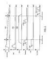
- FIG. 2is a timing chart of signals for an embodiment of a method for operating the CDS pixel of FIG. 1 ;
- FIG. 3is a flowchart illustrating an embodiment of a method for operating the CDS pixel of FIG. 1 ;
- FIG. 4is a simplified schematic diagram illustrating an embodiment of a configuration of the CDS pixel of FIG. 1 prior to sampling of the reset value;
- FIG. 5is a simplified schematic diagram illustrating an embodiment of a configuration of the CDS pixel of FIG. 1 during sampling of the reset value
- FIG. 6is a simplified schematic diagram illustrating an embodiment of a configuration of the CDS pixel of FIG. 1 during sampling of the signal value
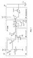
- FIG. 7is a simplified schematic diagram of a portion of an image sensor including a CDS pixel with a separate calibration voltage according to another embodiment.
- FIG. 8is a simplified schematic diagram of a portion of an image sensor including a CDS pixel with a precharging and calibration circuit coupled to a pixel output according to yet another embodiment.
- CDSCorrelated double sampling
- CDSincludes a technique of taking two samples of a signal out of the pixel and subtracting the first from the second to remove reset sampling noise. Generally, the sampling is performed once immediately following reset of the photodetector and once after the photodetector has been allowed to accumulate a charge due to change in lighting.
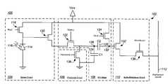
- FIG. 1A simplified schematic diagram of a portion of an image sensor 100 including an embodiment of a single, correlated double sampling (CDS) pixel 102 is shown in FIG. 1 .
- the CDS pixel 102includes a sensor circuit 104 to generate signals in response to electromagnetic radiation (light); a sample and hold (S/H) stage 106 to read-out or sample and store the signals; a precharge circuit 108 to precharge storage elements in the S/H stage; and a buffer/multiplexer circuit 110 to couple an output node of the S/H stage to a pixel output/column 112 .
- S/Hsample and hold
- precharge circuit 108to precharge storage elements in the S/H stage
- buffer/multiplexer circuit 110to couple an output node of the S/H stage to a pixel output/column 112 .
- the CDS pixel 102is generally one of multiple pixels in an array of pixels (not shown) arranged in multiple rows and multiple columns, pixel outputs from each column of the multiple rows of pixels coupled to shared column 112 to enable a pipelined or sequential readout of each row of pixels in the array.
- the array of pixelsis formed in a layer of semiconductor material on a common, shared wafer or substrate (not shown), which may include other elements and circuits of the image sensor.
- the sensor circuit 104includes a three transistor (3T)—like pixel front-end, which includes a photosensor or photodetector 114 to generate a signal in response to electromagnetic radiation 116 (light) received thereon.
- the photodetector 114can include one or more photodiodes, phototransistors, photoresistors or charge-coupled devices (CCDs), which generate a change in current, voltage or a charge in response to incident electromagnetic radiation on the photodetector.
- the photodetector 114includes a reverse-biased photodiode (PD) coupled between a positive pixel voltage supply (Vpix) and ground.
- PDreverse-biased photodiode
- the semiconductor material of which the PD 114 is fabricatedphotogenerates charge carriers, e.g. electrons, in proportion to the energy of electromagnetic radiation 116 received and to a time or integration period over which the PD is exposed to the electromagnetic radiation to generate a current (photocurrent) through the PD.
- a reset switching-element or transistor 118periodically resets the PD 114 to a fixed bias, clearing all accumulated charge on the photodetector due to photogenerated carriers at the beginning of every integration period.
- the sensor circuit 104further includes to a readout switching-element or transistor, such as a source follower amplifier (SF 120 ), having a drain connected or coupled to Vpix, a source coupled to an input of the S/H stage 106 , and a control node or gate coupled to the PD 114 .
- the SF 120generates a voltage signal or value corresponding to the charge accumulated on the PD 114 , and acts as a buffer to enable the charge on the PD to be sampled or measured substantially without altering or removing the accumulated charge.
- the S/H stage 106samples and holds or stores voltage signals from the sensor circuit 104 , and includes a sample switching-element or transistor 122 electrically connected or coupled to the source of the SF 120 to couple voltage signals (less a threshold voltage (V T ) of the SF) from the sensor circuit 104 to storage elements, such as capacitor-elements C 1 124 and C 2 126 connected in serial and in parallel with an output of the S/H stage 106 .
- V Tthreshold voltage
- C 2 126is serially coupled between an input and output of the S/H stage having a first or left-hand node (node 128 ) coupled to an output of the sample transistor 122 and a second or right hand node (node 130 ) coupled to a readout switching-element or transistor, such as a second source follower amplifier (SF 132 ), in the buffer/multiplexer circuit 110 .
- a first or left-hand node(node 128 ) coupled to an output of the sample transistor 122 and a second or right hand node (node 130 ) coupled to a readout switching-element or transistor, such as a second source follower amplifier (SF 132 ), in the buffer/multiplexer circuit 110 .
- SF 132second source follower amplifier
- the second or right hand node (node 130 ) of C 2 126is further coupled to a calibration switching-element or transistor 134 to couple C 2 126 to a predetermined, high DC calibration voltage (Vcalib) to enable C 2 to sample a reset value or signal of the PD 114 following reset of the sensor circuit 104 .
- Vcalibis selected to be within an order of magnitude of the expected reset value to be sure the full swing is maintained during subtraction (sampling).
- the calibration transistor 134is coupled to Vpix so that Vcalib is equal to Vpix.
- the calibration transistorcan instead be coupled to other nodes having another predetermined, high DC voltage (Vcalib).
- Capacitor-element C 1 124is also coupled to the output of the sample transistor 122 at node 128 and through a second node (not labeled) to a predetermined reference voltage.
- the second node of C 1 124is shown as being coupled in parallel with a precharge switching-element or transistor 136 to ground tap or line in the pixel 102 .
- the second node of C 1 124can alternatively be electrically coupled to any fixed voltage sufficiently below the positive pixel voltage supply (Vpix) to enable SF 120 to conduct, thereby ensuring a signal voltage or value from the sensor circuit 104 can be stored on C 1 .
- Vpixpositive pixel voltage supply
- C 1 124need not be coupled in parallel with the precharge transistor 136 , but can instead be separately coupled to a predetermined reference voltage or to electrical ground independently of the precharge transistor.
- capacitor-elements C 1 124 and C 2 126can both include independent, discrete capacitors, as shown schematically in FIG. 1 , alternatively the physical and electrical sizes of capacitor-element C 1 124 can be reduced, or a discrete capacitor eliminated entirely, by utilizing intrinsic capacitance formed between a plate of capacitor C 2 126 coupled to node 128 and an electrical ground of the common substrate (not shown). It will be appreciated Reducing the size of or eliminating C 1 124 significantly reduces an area in the pixel 102 occupied by non-light sensitive elements, and reducing the pitch or spacing between centers of the pixels, thereby improving fill factors of both the pixel and image sensor 100 , as compared to conventional eight transistor (8T) CDS pixels.
- 8Teight transistor
- fill factorit is meant a ratio of the area of photosensitive elements in the CDS pixel 102 or an array of pixels to a total area of the pixel or array. It will further be appreciated that increasing the fill factor also significantly increases the signal-to-noise (SNR) of the image sensor 100 as the SNR is directly related to the product of fill factor and quantum efficiency.
- SNRsignal-to-noise
- the in-pixel precharge circuit 108includes the precharge transistor 136 coupled to capacitor-elements C 1 124 and C 2 126 at node 128 to precharge C 1 and C 2 to a predetermined, precharge voltage prior to sampling a signal value from the sensor circuit 104 .
- Prechargingis desirable as the S/H stage 106 is driven by a simple source follower (SF 120 ) and, if a previous sampled value is higher or within a threshold voltage (V T ) of the SF (V T — SFI ) of the next sampled value, the SF will cut off and no sampling will take place.
- the pixel 102further includes a multiplexer or buffer/multiplexer circuit 110 to couple an output node of the S/H stage 106 to a pixel output or column 112 .
- the buffer/multiplexer circuit 110includes a source follower (SF) amplifier 132 that acts as a buffer and has a drain connected or coupled to Vpix and a source coupled to the column 112 through a row-select switching-element or transistor 138 .
- SFsource follower
- a R OW -S ELECT signalis applied to a control node or gate of the row-select transistor causing it to conduct and to transfer a voltage at a source of the second SF amplifier 132 to the column 112 .
- SF 120 , 132source followers amplifiers
- SF 120 and SF 132can be included in separate buffer stages (not shown) located between the sensor circuit 104 and S/H stage 106 , and/or between the S/H stage and buffer/multiplexer circuit 110 .
- the principle of operationincludes a phase during which a reset value of a voltage on the photodetector (PD 114 ) is sampled shortly after reset of the PD, and a second phase during which a signal value of the voltage on the PD 114 is sampled after the PD has been allowed to integrate charge photogenerated by electromagnetic radiation 116 (light) received thereon.
- PD 114a reset value of a voltage on the photodetector
- the first phasebegins with application of a RESET signal or pulse (Vreset 202 ) for a brief, predetermined period of time to the gate of the reset transistor 118 to clear any charge accumulated on the photodetector (PD 114 ) and reset the photodiode voltage (Vphotodiode 204 ) to Vpix.
- Vreset 202a RESET signal or pulse
- Vphotodiode 204the photodiode voltage
- Vphotodiode 204decreases from Vpix by a voltage value shown in FIG. 2 as ⁇ reset, due to gate-source crosstalk of the reset transistor 118 and the reset sampling noise also known as the KTC noise of the photodetector (PD 114 ).
- the reset sampling noise or KTC of the PD 114depends on the capacitance of the photodetector (PD 114 ), which is expressed in the voltage domain as shown in the following equation:
- V noise_pd ⁇ _rmsK ⁇ T C ( Eq . ⁇ 1 )
- KBoltzmann's constant ( ⁇ 1.38e-23) in joules per Kelvin
- Tis the diode's absolute temperature in degrees Kelvin
- Cis the capacitance of the PD 114 .
- a second blockthe circuit of FIG. 1 is configured in preparation for sampling the reset value by applying a C ALIB signal or pulse (Calib 206 ) to the gate of the calibration transistor 134 to couple node 130 to (Vpix), applying a S AMPLE signal or pulse (Sample 208 ) to the gate of the sampling transistor 122 , and, briefly, applying a P RECHARGE signal or pulse (Precharge 210 a ) to the gate of the precharge transistor 136 to precharge capacitor-elements C 1 124 and C 2 126 (block 306 ).
- a simplified schematic diagram illustrating an embodiment of the configuration of the CDS pixel 102 of FIG. 1 prior to sampling of the reset valueis shown in FIG. 4 .
- Vcalibis selected to be within an order of magnitude of the expected reset value (Vpix ⁇ reset), i.e., within the Vt of first SF 120 , to ensure that the SF conducts.
- Vpixis selected as Vcalib, however it will be understood that the calibration transistor 134 can instead be coupled to any other node having a predetermined, high DC voltage (Vcalib).
- the reset value of the voltage on the PD 114is sampled at a first time (t 0 ) (block 308 ).
- the sampling of the reset valueis accomplished on the trailing edge of the C ALIB signal or pulse (Calib 206 ) signal when the calibration transistor 134 is going off or opening.
- FIG. 5A simplified schematic diagram illustrating an embodiment of the configuration of the CDS pixel 102 of FIG. 1 during sampling of the reset value is shown in FIG. 5 .
- C 1is the capacitance of C 1 124
- C 2is the capacitance of C 2 126
- Vpixis the pixel high voltage
- resetis the decrease in PD 114 reset voltage following reset due to gate-source crosstalk and KTC noise of the PD
- Vt_sf 1is the threshold voltage of the first source follower SF 120 ).
- the sampling transistor 122continues to conduct while the calibration transistor 134 is going off to prevent introduction of KTC noise of C 1 124 on node 128 in addition to the KTC noise of C 2 126 on node 130 . More preferably, as shown in FIG. 2 the sampling transistor 122 continues to conduct throughout substantially the entire integration period.
- the value of the voltage on the PD 114is sampled after the PD has been allowed to integrate charge photogenerated by electromagnetic radiation 116 (light) received thereon.
- the reset value sampled in the previous stageis subtracted from the signal value to store on C 2 126 final output value or voltage for the pixel the change in voltage on the PD 114 due to light and the calibration voltage (Vcalib.
- Vcalibthe calibration voltage
- the circuit of FIG. 1is configured to sample the signal value by briefly applying a PRECHARGE signal or pulse (Precharge 210 b) to the gate of the precharge transistor 136 to precharge capacitor-elements C 1 124 and C 2 126 (block 310 ). Thereafter the sample signal (Sample 208 ) to the sampling transistor 122 is removed at a second time (ti) to sample the signal value and subtract the reset value sampled in the previous stage from the signal value stored on C 2 126 (block 312 ). In one embodiment, the sampling of the reset value is accomplished on the trailing edge of the CALIB signal or pulse (Calib 206 ) signal when the calibration transistor 134 is going off or opening.
- FIG. 6A simplified schematic diagram illustrating an embodiment of the configuration of the CDS pixel 102 of FIG. 1 during sampling of the signal value is shown in FIG. 6 .
- C 1is the capacitance of C 1 124
- C 2is the capacitance of C 2 126
- Vpixis the pixel high voltage
- resetis the decrease in PD 114 reset voltage following reset due to gate-source crosstalk and KTC noise of the PD
- a ⁇ lightis the decrease in PD 114 voltage following integration due to light incident on the PD
- Vt_sf 1is the threshold voltage of the first source follower SF 120
- Vyis the output voltage at node 130 of the S/H stage 106 .
- C 2is the capacitance of C 2 126
- Vpixis the pixel high voltage
- resetis the decrease in PD 114 reset voltage following reset due to gate-source crosstalk and KTC noise of the PD
- ⁇ Vlightis the decrease in PD 114 voltage following integration due to light incident on the PD
- Vt_sf 1is the threshold voltage of the first source follower SF 120
- Vyis the output voltage at node 130 of the S/H stage 106 .
- VyV pix ⁇ V light (Eq. 7)
- the output voltage of the S/H stage 106depends solely on the change in PD 114 voltage due to electromagnetic radiation 116 (light) and the calibration voltage (Vcalib) coupled to node 130 —Vpix in the example described above.
- Vcalibcalibration voltage
- the reset variations (reset) due to KTC noise of the PD 114 and fixed pattern noise (fpn) of the first source follower (SF 120 )are cancelled out.
- a R OW -S ELECT signal or pulse(Row-Select 212 ) is applied briefly to the gate of the row-select transistor 138 , which closes to couple the output of SF 132 and transfer the voltage at a source of the SF 140 to the column (block 314 ).
- the multiple row-select signals (select 212 ) with the dashed line in betweenare meant to illustrate a sequential read of pixels in different rows in a single column, as row after row is read out.
- the CDS pixel 102 output value on the column 112will be lower due to a threshold voltage (V T ) of the second source follower (SF 132 ), so the output value on the column will be:
- V columnV pix ⁇ V light ⁇ Vt — sf 2 (Eq. 8)
- the CDS pixel and correlated double sampling methodadvantageously enables snapshot operation of the image sensor in which substantially all of the pixels in an array operated to capture light or an image thereon at the substantially the same time. Briefly, for snapshot mode operation the falling edge of to the sample signal applied to the sample transistor 122 must be at substantially the same, predetermined integration time. As noted previously, this leads to the introduction of additional KTC noise of C 1 124 , which is expressed in the following equation:
- V noise_pd ⁇ _rmsK ⁇ T C ⁇ C -> C ⁇ ⁇ 1 ( Eq . ⁇ 9 )
- KBoltzmann's constant ( ⁇ 1.38e-23) in joules per Kelvin
- Tis the capacitor's absolute temperature in degrees Kelvin
- C 1is the capacitance the C 1 124 .
- V noise_rms ⁇ _pixelK ⁇ T C ⁇ ⁇ 1 + K ⁇ T C ⁇ ⁇ 2 ( Eq . ⁇ 10 )
- KBoltzmann's constant ( ⁇ 1.38e-23) in joules per Kelvin
- Tis the capacitor's absolute temperature in degrees Kelvin
- C 1is the capacitance the C 1 124
- C 2is the capacitance the C 2 126 .
- the capacitances of capacitance-elements C 1 124 and C 2 126is significantly larger than that of the capacitance of the PD 114 .
- significantly largerit is meant on the order of from about 5 to about 10 times the capacitance of the PD, or from about 15 to about 40 fF.
- the CDS pixel 102includes a calibration transistor 132 that is s not connected to the pixel high power supply (Vpix) but to a separate high voltage supply line (Vcalib).
- the precharge transistor 136can be located or coupled before the sample transistor 122 , reduce sample and hold leakage from the capacitance-elements C 1 124 and C 2 126 through the precharge transistor. Operation of the circuit of FIG. 7 is substantially unchanged from that described above with reference to FIGS. 2 and 3 , however it is noted the by the S AMPLE signal 208 must be maintained to the sampling transistor 122 during precharging of the capacitance-elements C 1 124 and C 2 126 .
- the CDS pixel 102further includes an in-pixel precharge circuit 108 and S/H stage 106 with a calibration transistor 134 coupled to pixel-output/column 112 .
- the image sensor 100further includes a number of switching-elements 140 and 142 to sequentially couple the column 112 to a column precharge supply 144 or current path ( 12 ) and a predetermined, high DC voltage (Vcalib 146 ) supply respectively.
- precharge capacitor-elements C 1 124 and C 2 126are coupled through the sample transistor 122 and precharge transistor 136 to the column 140 to precharge the capacitor-elements to a predetermined voltage before the sampling occurs.
- coupling C 1 124 and C 2 126 to the column 112 for precharging, rather than to an in-pixel ground tap or a separate precharge linedecreases a surface area of the pixel taken up with non-light sensitive elements substantially increasing the fill factor of the pixels and the array, thereby increasing the sensitivity of the image sensor 100 .
- the precharge transistor 136is coupled to the precharge current supply 144 through the same column 112 to which the buffer/multiplexer circuit 110 is coupled to readout the sampled signal from the pixel 102 .
- the precharge transistormay alternatively be coupled to any column in the array located near the pixel in which it is included.
- the precharge transistor 136can be coupled to a column different from that to which the buffer/multiplexer circuit 110 of the pixel 102 is coupled.
- the other columncan include, for example, the column to which an adjacent pixel located in a different column and possibly a different row in the array is coupled.
Landscapes
- Engineering & Computer Science (AREA)
- Multimedia (AREA)
- Signal Processing (AREA)
- Transforming Light Signals Into Electric Signals (AREA)
Abstract
Description
- The present disclosure relates generally to image sensors and more particularly to a correlated double sampling pixel and methods of operating the same.
- A design criterion in image sensors includes dynamic range, which is defined as a logarithmic ratio between the full scale voltage swing on the photodetector and the smallest detectable variation in photodiode output. Generally, the smallest detectable variation is dominated by reset sampling noise of the photodetector.
- A correlated double sampling pixel and method of operating the same are provided. In one embodiment, the pixel includes a sensor circuit to generate a voltage value corresponding to electromagnetic radiation received on a photodetector included therein, and a sample and hold (S/H) stage including a sample switching-element and first and second capacitor-elements. The first capacitor-element is coupled between an output of the sensor circuit through the sample switching-element and a predetermined reference potential. The second capacitor-element has a first node coupled to the output of the sensor circuit through the sample switching-element and a second node coupled in series with an output of the S/H stage, the second node of the second capacitor-element further coupled through a calibration switching-element to a calibration voltage to sample a reset voltage value on the photodetector at a first time at a beginning of an integration period following reset of the sensor circuit.
- These and various other features of the interface device and methods for using the same will be apparent upon reading of the following detailed description in conjunction with the accompanying drawings and the appended claims provided below, where:
FIG. 1 is a simplified schematic diagram of a portion of an image sensor including a correlated double sampling (CDS) pixel according to one embodiment;FIG. 2 is a timing chart of signals for an embodiment of a method for operating the CDS pixel ofFIG. 1 ;FIG. 3 is a flowchart illustrating an embodiment of a method for operating the CDS pixel ofFIG. 1 ;FIG. 4 is a simplified schematic diagram illustrating an embodiment of a configuration of the CDS pixel ofFIG. 1 prior to sampling of the reset value;FIG. 5 is a simplified schematic diagram illustrating an embodiment of a configuration of the CDS pixel ofFIG. 1 during sampling of the reset value;FIG. 6 is a simplified schematic diagram illustrating an embodiment of a configuration of the CDS pixel ofFIG. 1 during sampling of the signal value;FIG. 7 is a simplified schematic diagram of a portion of an image sensor including a CDS pixel with a separate calibration voltage according to another embodiment; andFIG. 8 is a simplified schematic diagram of a portion of an image sensor including a CDS pixel with a precharging and calibration circuit coupled to a pixel output according to yet another embodiment.- The drawings described are only schematic and are non-limiting. In the drawings, the size of some of the elements may be exaggerated and not drawn to scale for illustrative purposes. The dimensions and the relative dimensions may not correspond to actual reductions to practice of the invention. For purposes of clarity, many of the details of image sensors in general and to image sensors including arrays of active pixels in particular, which are widely known and not relevant to the present control system and method have been omitted from the following description.
- Correlated double sampling (CDS) may be used to reduce the impact of reset sampling noise on dynamic range. CDS includes a technique of taking two samples of a signal out of the pixel and subtracting the first from the second to remove reset sampling noise. Generally, the sampling is performed once immediately following reset of the photodetector and once after the photodetector has been allowed to accumulate a charge due to change in lighting.
- A simplified schematic diagram of a portion of an
image sensor 100 including an embodiment of a single, correlated double sampling (CDS)pixel 102 is shown inFIG. 1 . TheCDS pixel 102 includes asensor circuit 104 to generate signals in response to electromagnetic radiation (light); a sample and hold (S/H)stage 106 to read-out or sample and store the signals; aprecharge circuit 108 to precharge storage elements in the S/H stage; and a buffer/multiplexer circuit 110 to couple an output node of the S/H stage to a pixel output/column 112. TheCDS pixel 102 is generally one of multiple pixels in an array of pixels (not shown) arranged in multiple rows and multiple columns, pixel outputs from each column of the multiple rows of pixels coupled to sharedcolumn 112 to enable a pipelined or sequential readout of each row of pixels in the array. The array of pixels is formed in a layer of semiconductor material on a common, shared wafer or substrate (not shown), which may include other elements and circuits of the image sensor. - Referring to
FIG. 1 , thesensor circuit 104 includes a three transistor (3T)—like pixel front-end, which includes a photosensor orphotodetector 114 to generate a signal in response to electromagnetic radiation116 (light) received thereon. Thephotodetector 114 can include one or more photodiodes, phototransistors, photoresistors or charge-coupled devices (CCDs), which generate a change in current, voltage or a charge in response to incident electromagnetic radiation on the photodetector. In the embodiment shown, thephotodetector 114 includes a reverse-biased photodiode (PD) coupled between a positive pixel voltage supply (Vpix) and ground. When exposed toelectromagnetic radiation 116 the semiconductor material of which thePD 114 is fabricated photogenerates charge carriers, e.g. electrons, in proportion to the energy ofelectromagnetic radiation 116 received and to a time or integration period over which the PD is exposed to the electromagnetic radiation to generate a current (photocurrent) through the PD. A reset switching-element ortransistor 118 periodically resets thePD 114 to a fixed bias, clearing all accumulated charge on the photodetector due to photogenerated carriers at the beginning of every integration period. Thesensor circuit 104 further includes to a readout switching-element or transistor, such as a source follower amplifier (SF120), having a drain connected or coupled to Vpix, a source coupled to an input of the S/H stage 106, and a control node or gate coupled to thePD 114. The SF120 generates a voltage signal or value corresponding to the charge accumulated on thePD 114, and acts as a buffer to enable the charge on the PD to be sampled or measured substantially without altering or removing the accumulated charge. - The S/
H stage 106 samples and holds or stores voltage signals from thesensor circuit 104, and includes a sample switching-element ortransistor 122 electrically connected or coupled to the source of the SF120 to couple voltage signals (less a threshold voltage (VT) of the SF) from thesensor circuit 104 to storage elements, such as capacitor-elements C1 124 andC2 126 connected in serial and in parallel with an output of the S/H stage 106. More specifically,C2 126 is serially coupled between an input and output of the S/H stage having a first or left-hand node (node128) coupled to an output of thesample transistor 122 and a second or right hand node (node130) coupled to a readout switching-element or transistor, such as a second source follower amplifier (SF132), in the buffer/multiplexer circuit 110. - The second or right hand node (node130) of
C2 126 is further coupled to a calibration switching-element ortransistor 134 tocouple C2 126 to a predetermined, high DC calibration voltage (Vcalib) to enable C2 to sample a reset value or signal of thePD 114 following reset of thesensor circuit 104. As explained in greater detail below, Vcalib is selected to be within an order of magnitude of the expected reset value to be sure the full swing is maintained during subtraction (sampling). In the embodiments shown inFIG. 1 , thecalibration transistor 134 is coupled to Vpix so that Vcalib is equal to Vpix. However, it will be understood that this need not be the case, and that in other embodiments, such as those described inFIGS. 7 and 8 below, the calibration transistor can instead be coupled to other nodes having another predetermined, high DC voltage (Vcalib). - Capacitor-
element C1 124 is also coupled to the output of thesample transistor 122 atnode 128 and through a second node (not labeled) to a predetermined reference voltage. InFIG. 1 the second node of C1124 is shown as being coupled in parallel with a precharge switching-element ortransistor 136 to ground tap or line in thepixel 102. However, it will be understood by those skilled in the art, that this need not be the case, and that the second node ofC1 124 can alternatively be electrically coupled to any fixed voltage sufficiently below the positive pixel voltage supply (Vpix) to enable SF120 to conduct, thereby ensuring a signal voltage or value from thesensor circuit 104 can be stored on C1. It will further be understood that in still other embodiments, as described in detail below, C1124 need not be coupled in parallel with theprecharge transistor 136, but can instead be separately coupled to a predetermined reference voltage or to electrical ground independently of the precharge transistor. - Although capacitor-elements C1124 and
C2 126 can both include independent, discrete capacitors, as shown schematically inFIG. 1 , alternatively the physical and electrical sizes of capacitor-element C1 124 can be reduced, or a discrete capacitor eliminated entirely, by utilizing intrinsic capacitance formed between a plate ofcapacitor C2 126 coupled tonode 128 and an electrical ground of the common substrate (not shown). It will be appreciated Reducing the size of or eliminatingC1 124 significantly reduces an area in thepixel 102 occupied by non-light sensitive elements, and reducing the pitch or spacing between centers of the pixels, thereby improving fill factors of both the pixel andimage sensor 100, as compared to conventional eight transistor (8T) CDS pixels. By fill factor it is meant a ratio of the area of photosensitive elements in theCDS pixel 102 or an array of pixels to a total area of the pixel or array. It will further be appreciated that increasing the fill factor also significantly increases the signal-to-noise (SNR) of theimage sensor 100 as the SNR is directly related to the product of fill factor and quantum efficiency. - As noted above, the in-
pixel precharge circuit 108 includes theprecharge transistor 136 coupled to capacitor-elements C1 124 andC2 126 atnode 128 to precharge C1 and C2 to a predetermined, precharge voltage prior to sampling a signal value from thesensor circuit 104. Precharging is desirable as the S/H stage 106 is driven by a simple source follower (SF120) and, if a previous sampled value is higher or within a threshold voltage (VT) of the SF (VT— SFI) of the next sampled value, the SF will cut off and no sampling will take place. Thus, without precharging or clearing the capacitor-elements C1 124 andC2 126 in the S/H stage 106 the image sensed will rise to a black or blank image over time. Another reason for precharging capacitor-elements C1124 andC2 126 is to help reduce image lag, that is a persistence or incomplete erasure of a previously sampled value that could lead to errors in imaging. - As noted above, the
pixel 102 further includes a multiplexer or buffer/multiplexer circuit 110 to couple an output node of the S/H stage 106 to a pixel output orcolumn 112. In the embodiment shown inFIG. 1 the buffer/multiplexer circuit 110 includes a source follower (SF)amplifier 132 that acts as a buffer and has a drain connected or coupled to Vpix and a source coupled to thecolumn 112 through a row-select switching-element ortransistor 138. For reading, a ROW -SELECT signal is applied to a control node or gate of the row-select transistor causing it to conduct and to transfer a voltage at a source of thesecond SF amplifier 132 to thecolumn 112. - Although the
sensor circuit 104 and buffer/multiplexer circuit 110 are shown as including source followers amplifiers (SF120,132), which serve as buffers it will be appreciated that other amplifier configurations can also be used. It will further by appreciated that SF120 and SF132, can be included in separate buffer stages (not shown) located between thesensor circuit 104 and S/H stage 106, and/or between the S/H stage and buffer/multiplexer circuit 110. - An embodiment of a method for operating the
CDS pixel 102 will now be described with reference toFIG. 1 , the timing diagram ofFIG. 2 and the flowchart ofFIG. 3 . Briefly, the principle of operation includes a phase during which a reset value of a voltage on the photodetector (PD114) is sampled shortly after reset of the PD, and a second phase during which a signal value of the voltage on thePD 114 is sampled after the PD has been allowed to integrate charge photogenerated by electromagnetic radiation116 (light) received thereon. - Referring to
FIGS. 2 and 3 , in a first block (block302) the first phase begins with application of a RESET signal or pulse (Vreset202) for a brief, predetermined period of time to the gate of thereset transistor 118 to clear any charge accumulated on the photodetector (PD114) and reset the photodiode voltage (Vphotodiode204) to Vpix. After the RESET signal is removedVphotodiode 204 decreases from Vpix by a voltage value shown inFIG. 2 as Δreset, due to gate-source crosstalk of thereset transistor 118 and the reset sampling noise also known as the KTC noise of the photodetector (PD114). The reset sampling noise or KTC of thePD 114 depends on the capacitance of the photodetector (PD114), which is expressed in the voltage domain as shown in the following equation: - where K is Boltzmann's constant (˜1.38e-23) in joules per Kelvin, T is the diode's absolute temperature in degrees Kelvin, and C is the capacitance of the
PD 114. - After resetting the
PD 114, in a second block (block304) the circuit ofFIG. 1 is configured in preparation for sampling the reset value by applying a CALIB signal or pulse (Calib206) to the gate of thecalibration transistor 134 tocouple node 130 to (Vpix), applying a SAMPLE signal or pulse (Sample208) to the gate of thesampling transistor 122, and, briefly, applying a PRECHARGE signal or pulse (Precharge 210a) to the gate of theprecharge transistor 136 to precharge capacitor-elements C1 124 and C2126 (block306). A simplified schematic diagram illustrating an embodiment of the configuration of theCDS pixel 102 ofFIG. 1 prior to sampling of the reset value is shown inFIG. 4 . - As noted above with respect to
FIG. 1 , Vcalib is selected to be within an order of magnitude of the expected reset value (Vpix−Δreset), i.e., within the Vt offirst SF 120, to ensure that the SF conducts. In the embodiments shown inFIGS. 1 and 4 , Vpix is selected as Vcalib, however it will be understood that thecalibration transistor 134 can instead be coupled to any other node having a predetermined, high DC voltage (Vcalib). - After capacitor-
elements C1 124 andC2 126 been precharged, the reset value of the voltage on thePD 114 is sampled at a first time (t0) (block308). In one embodiment, the sampling of the reset value is accomplished on the trailing edge of the CALIB signal or pulse (Calib206) signal when thecalibration transistor 134 is going off or opening. A simplified schematic diagram illustrating an embodiment of the configuration of theCDS pixel 102 ofFIG. 1 during sampling of the reset value is shown inFIG. 5 . - The charges (Q) sampled or stored on
C1 124 and onC2 126 following sampling of the reset values is as follows:
Qreset— c2=C2·((Vpix−Δreset−Vt—sf1)−Vpix)=C2·(″Δreset−Vt—sf1) (Eq. 2)
and
Qreset— c1=C1·((Vpix−Δreset−Vt—sf1)) (Eq. 3)- where C1 is the capacitance of
C1 124, C2 is the capacitance ofC2 126, Vpix is the pixel high voltage, reset is the decrease inPD 114 reset voltage following reset due to gate-source crosstalk and KTC noise of the PD, and Vt_sf1 is the threshold voltage of the first source follower SF120). - As indicated by the S
AMPLE signal 208 ofFIG. 2 and the simplified schematic ofFIG. 5 , thesampling transistor 122 continues to conduct while thecalibration transistor 134 is going off to prevent introduction of KTC noise ofC1 124 onnode 128 in addition to the KTC noise ofC2 126 onnode 130. More preferably, as shown inFIG. 2 thesampling transistor 122 continues to conduct throughout substantially the entire integration period. - Next, during the signal sampling phase the value of the voltage on the
PD 114 is sampled after the PD has been allowed to integrate charge photogenerated by electromagnetic radiation116 (light) received thereon. At the same time the signal value is sampled, the reset value sampled in the previous stage is subtracted from the signal value to store onC2 126 final output value or voltage for the pixel the change in voltage on thePD 114 due to light and the calibration voltage (Vcalib. It will be appreciated that because the subtraction is accomplished within theCDS pixel 102, without the need for additional amplifier-elements that the CDS pixel of the present invention as well as any image sensor made therewith can provide substantially improved fill factors and efficiency over conventional CDS pixels. It will further be appreciated that because subtraction is accomplished substantially simultaneously with the sampling of the signal value, there is substantially no reduction in readout speed as compared to a conventional non-CDS pixel. - Referring to
FIGS. 2 and 3 , the circuit ofFIG. 1 is configured to sample the signal value by briefly applying a PRECHARGE signal or pulse (Precharge 210b) to the gate of theprecharge transistor 136 to precharge capacitor-elements C1 124 and C2126 (block310). Thereafter the sample signal (Sample208) to thesampling transistor 122 is removed at a second time (ti) to sample the signal value and subtract the reset value sampled in the previous stage from the signal value stored on C2126 (block312). In one embodiment, the sampling of the reset value is accomplished on the trailing edge of the CALIB signal or pulse (Calib206) signal when thecalibration transistor 134 is going off or opening. A simplified schematic diagram illustrating an embodiment of the configuration of theCDS pixel 102 ofFIG. 1 during sampling of the signal value is shown inFIG. 6 . - The charges or values stored on capacitor-
elements C1 124 andC2 126 following the sampling of the signal value and the subtraction of the reset value are as follows:
Qsignal— c2=C·((Vpix−Δreset−ΔVlight−Vt—sf1)−Vy) (Eq. 4)
and
Qsignal— c1=C·((Vpix−Δreset−ΔVlight−Vt—sf1)) (Eq. 5)- where C1 is the capacitance of
C1 124, C2 is the capacitance ofC2 126, Vpix is the pixel high voltage, reset is the decrease inPD 114 reset voltage following reset due to gate-source crosstalk and KTC noise of the PD, A Δlight is the decrease inPD 114 voltage following integration due to light incident on the PD, Vt_sf1 is the threshold voltage of the first source follower SF120) and Vy is the output voltage atnode 130 of the S/H stage 106. - Referring to
FIG. 6 , it is seen that because both nodes ofC1 124 are driven only the charge onC2 126 has any effect on the pixel output. Moreover, due to the principal of conservation of charge Qreset_C2=Qsignal_C2, thus:
C2·(−Δreset−Vt—sf1)=C2·((Vpix−Δreset−ΔVlight−Vt—sf1)−Vy) (Eq. 6)- where C2 is the capacitance of
C2 126, Vpix is the pixel high voltage, reset is the decrease inPD 114 reset voltage following reset due to gate-source crosstalk and KTC noise of the PD, ΔVlight is the decrease inPD 114 voltage following integration due to light incident on the PD, Vt_sf1 is the threshold voltage of the first source follower SF120) and Vy is the output voltage atnode 130 of the S/H stage 106. - This reduces to:
Vy=Vpix−ΔVlight (Eq. 7)- It is noted that the output voltage of the S/
H stage 106 depends solely on the change inPD 114 voltage due to electromagnetic radiation116 (light) and the calibration voltage (Vcalib) coupled tonode 130—Vpix in the example described above. Thus, the reset variations (reset) due to KTC noise of thePD 114 and fixed pattern noise (fpn) of the first source follower (SF120) are cancelled out. - After the signal value has been sampled and the subtraction performed, a R
OW -SELECT signal or pulse (Row-Select212) is applied briefly to the gate of the row-select transistor 138, which closes to couple the output ofSF 132 and transfer the voltage at a source of theSF 140 to the column (block314). The multiple row-select signals (select212) with the dashed line in between are meant to illustrate a sequential read of pixels in different rows in a single column, as row after row is read out. - Finally, it is noted that the
CDS pixel 102 output value on thecolumn 112 will be lower due to a threshold voltage (VT) of the second source follower (SF132), so the output value on the column will be:
Vcolumn=Vpix−ΔVlight−Vt—sf2 (Eq. 8)- where Vcolumn is the output value on the column, Vpix is the pixel high voltage, ΔVlight is the decrease in
PD 114 voltage following integration due to light incident on the PD, and Vt_sf2 is the threshold voltage of the second source follower (SF132). In another aspect, the CDS pixel and correlated double sampling method advantageously enables snapshot operation of the image sensor in which substantially all of the pixels in an array operated to capture light or an image thereon at the substantially the same time. Briefly, for snapshot mode operation the falling edge of to the sample signal applied to thesample transistor 122 must be at substantially the same, predetermined integration time. As noted previously, this leads to the introduction of additional KTC noise ofC1 124, which is expressed in the following equation: - where K is Boltzmann's constant (˜1.38e-23) in joules per Kelvin, T is the capacitor's absolute temperature in degrees Kelvin, and C1 is the capacitance the
C1 124. Together with the KTC noise after reset sampling this additional KTC noise will yield a total KTC noise (rms) of: - where K is Boltzmann's constant (˜1.38e-23) in joules per Kelvin, T is the capacitor's absolute temperature in degrees Kelvin, C1 is the capacitance the
C1 124 and C2 is the capacitance theC2 126. - Accordingly, in those embodiments capable of or intended to operate in snapshot mode it is desirable that the capacitances of capacitance-
elements C1 124 andC2 126 is significantly larger than that of the capacitance of thePD 114. By significantly larger it is meant on the order of from about5 to about10 times the capacitance of the PD, or from about 15 to about 40 fF. - In an alternative embodiment, shown in
FIG. 7 , theCDS pixel 102 includes acalibration transistor 132 that is s not connected to the pixel high power supply (Vpix) but to a separate high voltage supply line (Vcalib). Optionally, as also shown inFIG. 7 , theprecharge transistor 136 can be located or coupled before thesample transistor 122, reduce sample and hold leakage from the capacitance-elements C1 124 andC2 126 through the precharge transistor. Operation of the circuit ofFIG. 7 is substantially unchanged from that described above with reference toFIGS. 2 and 3 , however it is noted the by the SAMPLE signal 208 must be maintained to thesampling transistor 122 during precharging of the capacitance-elements C1 124 andC2 126. - In yet another alternative embodiment, shown in
FIG. 8 , theCDS pixel 102 further includes an in-pixelprecharge circuit 108 and S/H stage 106 with acalibration transistor 134 coupled to pixel-output/column 112. Referring toFIG. 8 , Theimage sensor 100 further includes a number of switching-elements column 112 to a columnprecharge supply 144 or current path (12) and a predetermined, high DC voltage (Vcalib146) supply respectively. During precharge capacitor-elements C1 124 andC2 126 are coupled through thesample transistor 122 andprecharge transistor 136 to thecolumn 140 to precharge the capacitor-elements to a predetermined voltage before the sampling occurs. It will be appreciated thatcoupling C1 124 andC2 126 to thecolumn 112 for precharging, rather than to an in-pixel ground tap or a separate precharge line decreases a surface area of the pixel taken up with non-light sensitive elements substantially increasing the fill factor of the pixels and the array, thereby increasing the sensitivity of theimage sensor 100. - In the embodiment shown in
FIG. 8 , theprecharge transistor 136 is coupled to the prechargecurrent supply 144 through thesame column 112 to which the buffer/multiplexer circuit 110 is coupled to readout the sampled signal from thepixel 102. The precharge transistor may alternatively be coupled to any column in the array located near the pixel in which it is included. For example, in other embodiments theprecharge transistor 136 can be coupled to a column different from that to which the buffer/multiplexer circuit 110 of thepixel 102 is coupled. The other column can include, for example, the column to which an adjacent pixel located in a different column and possibly a different row in the array is coupled. - Thus, embodiments of a CDS pixel and method for correlated double sampling of the pixel that increases Dynamic Range and fill factor of the image sensor, while decreasing readout time have been described. Although the present disclosure has been described with reference to specific exemplary embodiments, it will be evident that various modifications and changes may be made to these embodiments without departing from the broader spirit and scope of the disclosure. Accordingly, the specification and drawings are to be regarded in an illustrative rather than a restrictive sense.
- The Abstract of the Disclosure is provided to comply with 37 C.F.R. §1.72(b), requiring an abstract that will allow the reader to quickly ascertain the nature of the technical disclosure. It is submitted with the understanding that it will not be used to interpret or limit the scope or meaning of the claims. In addition, in the foregoing Detailed Description, it can be seen that various features are grouped together in a single embodiment for the purpose of streamlining the disclosure. This method of disclosure is not to be interpreted as reflecting an intention that the claimed embodiments require more features than are expressly recited in each claim. Rather, as the following claims reflect, inventive subject matter lies in less than all features of a single disclosed embodiment. Thus, the following claims are hereby incorporated into the Detailed Description, with each claim standing on its own as a separate embodiment.
- In the forgoing description, for purposes of explanation, numerous specific details have been set forth in order to provide a thorough understanding of the control system and method of the present disclosure. It will be evident however to one skilled in the art that the present interface device and method may be practiced without these specific details. In other instances, well-known structures, and techniques are not shown in detail or are shown in block diagram form in order to avoid unnecessarily obscuring an understanding of this description.
- Reference in the description to “one embodiment” or “an embodiment” means that a particular feature, structure, or characteristic described in connection with the embodiment is included in at least one embodiment of the control system or method. The appearances of the phrase “one embodiment” in various places in the specification do not necessarily all refer to the same embodiment. The term “to couple” as used herein may include both to directly electrically connect two or more components or elements and to indirectly connect through one or more intervening components.
Claims (20)
Priority Applications (2)
| Application Number | Priority Date | Filing Date | Title |
|---|---|---|---|
| US12/284,901US8059173B2 (en) | 2008-09-26 | 2008-09-26 | Correlated double sampling pixel and method |
| EP09252239.0AEP2169948A3 (en) | 2008-09-26 | 2009-09-21 | Correlated double sampling pixel |
Applications Claiming Priority (1)
| Application Number | Priority Date | Filing Date | Title |
|---|---|---|---|
| US12/284,901US8059173B2 (en) | 2008-09-26 | 2008-09-26 | Correlated double sampling pixel and method |
Publications (2)
| Publication Number | Publication Date |
|---|---|
| US20100079632A1true US20100079632A1 (en) | 2010-04-01 |
| US8059173B2 US8059173B2 (en) | 2011-11-15 |
Family
ID=41506453
Family Applications (1)
| Application Number | Title | Priority Date | Filing Date |
|---|---|---|---|
| US12/284,901Active2030-02-03US8059173B2 (en) | 2008-09-26 | 2008-09-26 | Correlated double sampling pixel and method |
Country Status (2)
| Country | Link |
|---|---|
| US (1) | US8059173B2 (en) |
| EP (1) | EP2169948A3 (en) |
Cited By (11)
| Publication number | Priority date | Publication date | Assignee | Title |
|---|---|---|---|---|
| US20110141078A1 (en)* | 2009-09-25 | 2011-06-16 | Stmicroelectronics (Research & Development) Limite | Ambient light detection |
| US20120312967A1 (en)* | 2011-06-10 | 2012-12-13 | Yannick De Wit | Pixel and method |
| JP2013183442A (en)* | 2012-03-05 | 2013-09-12 | Olympus Corp | Solid state imaging apparatus and imaging apparatus |
| US20160088251A1 (en)* | 2013-05-17 | 2016-03-24 | Brigates Microelectronics (Kunshan) Co., Ltd. | Cmos image sensor, pixel unit and control method thereof |
| CN107786821A (en)* | 2016-08-29 | 2018-03-09 | 意法半导体(R&D)有限公司 | Pixel circuit and method of operation thereof |
| WO2019211949A1 (en)* | 2018-05-02 | 2019-11-07 | Sony Semiconductor Solutions Corporation | Solid-state image pickup element and image pickup apparatus |
| US10771725B1 (en)* | 2019-07-03 | 2020-09-08 | Himax Imaging Limited | Pixel circuit |
| US20210160448A1 (en)* | 2019-11-27 | 2021-05-27 | Samsung Electronics Co., Ltd. | Image sensor, imaging device having the image sensor, and operating method thereof |
| US11215716B2 (en)* | 2018-05-09 | 2022-01-04 | Beijing Boe Optoelectronics Technology Co., Ltd. | Photo-detecting circuit, driving method thereof and flat panel detector |
| US20220094864A1 (en)* | 2020-09-18 | 2022-03-24 | Samsung Electronics Co., Ltd. | Image sensor |
| US20240205556A1 (en)* | 2022-12-14 | 2024-06-20 | Samsung Electronics Co., Ltd. | Image sensor having high dynamic range |
Families Citing this family (4)
| Publication number | Priority date | Publication date | Assignee | Title |
|---|---|---|---|---|
| KR101573408B1 (en)* | 2009-04-29 | 2015-12-02 | 삼성전자주식회사 | IMAGE SENSOR WITH NOISE REMOVING MEANS, IMAGE PICKUP DEVICE HAVING THE SAME, AND METHOD THEREOF |
| KR102196713B1 (en) | 2014-04-21 | 2020-12-30 | 삼성전자주식회사 | Arithmetic memory device, Image sensor comprising the same and method for operating the arithmetic memory device |
| KR102618490B1 (en)* | 2018-12-13 | 2023-12-27 | 삼성전자주식회사 | Image sensor and method of driving the same |
| CN112906444B (en)* | 2019-12-04 | 2023-11-14 | 北京小米移动软件有限公司 | Active pixel sensor arrays, display panels, electronic devices |
Citations (34)
| Publication number | Priority date | Publication date | Assignee | Title |
|---|---|---|---|---|
| US5128534A (en)* | 1990-07-17 | 1992-07-07 | Hughes Aircraft Company | High charge capacity focal plane array readout cell |
| US5461425A (en)* | 1994-02-15 | 1995-10-24 | Stanford University | CMOS image sensor with pixel level A/D conversion |
| US5668375A (en)* | 1996-08-26 | 1997-09-16 | General Electric Company | Fast scan reset for a large area x-ray detector |
| US5909026A (en)* | 1996-11-12 | 1999-06-01 | California Institute Of Technology | Integrated sensor with frame memory and programmable resolution for light adaptive imaging |
| US5990948A (en)* | 1996-02-29 | 1999-11-23 | Kabushiki Kaisha Toshiba | Noise cancelling circuit for pixel signals and an image pickup device using the noise cancelling circuit |
| US6166367A (en)* | 1998-03-26 | 2000-12-26 | Photobit Corporation | Programmable analog arithmetic circuit for imaging sensor |
| US6225670B1 (en)* | 1997-06-04 | 2001-05-01 | Imec | Detector for electromagnetic radiation, pixel structure with high sensitivity using such detector and method of manufacturing such detector |
| US20030011694A1 (en)* | 2001-07-16 | 2003-01-16 | Bart Dierickx | Method to adjust the signal level of an active pixel and corresponding active pixel |
| US20030011829A1 (en)* | 2001-07-16 | 2003-01-16 | Bart Dierickx | Methods and devices for reading out an image sensor with reduced delay time between lines |
| US6545303B1 (en)* | 2001-11-06 | 2003-04-08 | Fillfactory | Method to increase conversion gain of an active pixel, and corresponding active pixel |
| US6787749B1 (en)* | 1996-11-12 | 2004-09-07 | California Institute Of Technology | Integrated sensor with frame memory and programmable resolution for light adaptive imaging |
| US20040212704A1 (en)* | 1998-08-06 | 2004-10-28 | Cynthia Bell | Reducing the effect of noise in an imaging system |
| US6812539B1 (en)* | 2003-04-10 | 2004-11-02 | Micron Technology, Inc. | Imager light shield |
| US6836291B1 (en)* | 1998-04-30 | 2004-12-28 | Minolta Co., Ltd. | Image pickup device with integral amplification |
| US20050088553A1 (en)* | 2003-09-09 | 2005-04-28 | Kazunobu Kuwazawa | Solid state imaging device and method of driving the same |
| US20050092895A1 (en)* | 2003-10-30 | 2005-05-05 | Fossum Eric R. | In-pixel kTC noise suppression using circuit techniques |
| US20050099517A1 (en)* | 2003-09-19 | 2005-05-12 | Kazunobu Kuwazawa | Solid state imaging device and method of driving the same |
| US20050235215A1 (en)* | 2004-04-01 | 2005-10-20 | Dunn Michael H | Virtual flip chart method and apparatus |
| US20050270394A1 (en)* | 2004-05-25 | 2005-12-08 | Bart Dierickx | Method and pixel for performing correlated double sampling |
| US7113213B2 (en)* | 1995-08-11 | 2006-09-26 | Tokyo Shibaura Electric Co | Image system, solid-state imaging semiconductor integrated circuit device used in the image system, and difference output method used for the image system |
| US7289148B1 (en)* | 1997-09-22 | 2007-10-30 | Cypress Semiconductor Corporation (Belgium) Bvba | Devices and methods for improving the image quality in an image sensor |
| US20080018763A1 (en)* | 2006-07-20 | 2008-01-24 | Pentax Corporation | Imaging device |
| US7379109B2 (en)* | 2003-03-20 | 2008-05-27 | Matsushita Electric Industrial Co., Ltd. | Solid-state image sensing apparatus and driving method thereof |
| US7408443B2 (en)* | 2003-01-13 | 2008-08-05 | Samsung Electronics Co., Ltd. | Circuit and method for reducing fixed pattern noise |
| US20080218620A1 (en)* | 2007-03-08 | 2008-09-11 | Imagerlabs Inc. | Ultra low noise cmos imager |
| US20080259195A1 (en)* | 2007-04-20 | 2008-10-23 | Olympus Corporation | Solid-state imaging apparatus |
| US20080297627A1 (en)* | 2007-05-30 | 2008-12-04 | Olympus Corporation | Solid-state imaging apparatus |
| US7479995B2 (en)* | 2005-05-19 | 2009-01-20 | Digital Imaging Systems Gmbh | On chip real time FPN correction without imager size memory |
| US7479994B2 (en)* | 2004-11-23 | 2009-01-20 | Digital Imaging Systems Gmbh | Image sensor having resolution adjustment employing an analog column averaging/row averaging for high intensity light or row binning for low intensity light |
| US20090021619A1 (en)* | 2004-01-13 | 2009-01-22 | Shigetaka Kasuga | Solid state image pickup device and camera using the same |
| US7515183B2 (en)* | 2004-11-23 | 2009-04-07 | Digital Imaging Systems Gmbh | Column averaging/row binning circuit for image sensor resolution adjustment in lower intensity light environment |
| US7548261B2 (en)* | 2004-11-30 | 2009-06-16 | Digital Imaging Systems Gmbh | Column averaging/row averaging circuit for image sensor resolution adjustment in high intensity light environment |
| US20100020213A1 (en)* | 2005-02-28 | 2010-01-28 | Rick Mauritzson | Imager row-wise noise correction |
| US7825967B2 (en)* | 2004-07-12 | 2010-11-02 | Aptina Imaging Corporation | Column-wise clamp voltage driver for suppression of noise in an imager |
Family Cites Families (6)
| Publication number | Priority date | Publication date | Assignee | Title |
|---|---|---|---|---|
| US5742047A (en)* | 1996-10-01 | 1998-04-21 | Xerox Corporation | Highly uniform five volt CMOS image photodiode sensor array with improved contrast ratio and dynamic range |
| US6046444A (en) | 1997-12-08 | 2000-04-04 | Intel Corporation | High sensitivity active pixel with electronic shutter |
| US6417504B1 (en)* | 2000-09-29 | 2002-07-09 | Innovative Technology Licensing, Llc | Compact ultra-low noise high-bandwidth pixel amplifier for single-photon readout of photodetectors |
| US6847400B2 (en)* | 2001-03-22 | 2005-01-25 | Xerox Corporation | Photosensitive apparatus wherein an initial charge on a photodiode is sampled and substracted during readout |
| JP4426273B2 (en) | 2003-05-22 | 2010-03-03 | イノテック株式会社 | MOS type solid-state imaging device and manufacturing method thereof |
| WO2008064435A1 (en)* | 2006-11-29 | 2008-06-05 | Cypress Semiconductor Corporation (Belgium) Bvba | Pixel structure having shielded storage node |
- 2008
- 2008-09-26USUS12/284,901patent/US8059173B2/enactiveActive
- 2009
- 2009-09-21EPEP09252239.0Apatent/EP2169948A3/ennot_activeWithdrawn
Patent Citations (43)
| Publication number | Priority date | Publication date | Assignee | Title |
|---|---|---|---|---|
| US5128534A (en)* | 1990-07-17 | 1992-07-07 | Hughes Aircraft Company | High charge capacity focal plane array readout cell |
| US5461425A (en)* | 1994-02-15 | 1995-10-24 | Stanford University | CMOS image sensor with pixel level A/D conversion |
| US7113213B2 (en)* | 1995-08-11 | 2006-09-26 | Tokyo Shibaura Electric Co | Image system, solid-state imaging semiconductor integrated circuit device used in the image system, and difference output method used for the image system |
| US5990948A (en)* | 1996-02-29 | 1999-11-23 | Kabushiki Kaisha Toshiba | Noise cancelling circuit for pixel signals and an image pickup device using the noise cancelling circuit |
| US5668375A (en)* | 1996-08-26 | 1997-09-16 | General Electric Company | Fast scan reset for a large area x-ray detector |
| US5909026A (en)* | 1996-11-12 | 1999-06-01 | California Institute Of Technology | Integrated sensor with frame memory and programmable resolution for light adaptive imaging |
| US6057539A (en)* | 1996-11-12 | 2000-05-02 | California Institute Of Technology | Integrated sensor with frame memory and programmable resolution for light adaptive imaging |
| US6787749B1 (en)* | 1996-11-12 | 2004-09-07 | California Institute Of Technology | Integrated sensor with frame memory and programmable resolution for light adaptive imaging |
| US6225670B1 (en)* | 1997-06-04 | 2001-05-01 | Imec | Detector for electromagnetic radiation, pixel structure with high sensitivity using such detector and method of manufacturing such detector |
| US7289148B1 (en)* | 1997-09-22 | 2007-10-30 | Cypress Semiconductor Corporation (Belgium) Bvba | Devices and methods for improving the image quality in an image sensor |
| US6166367A (en)* | 1998-03-26 | 2000-12-26 | Photobit Corporation | Programmable analog arithmetic circuit for imaging sensor |
| US6836291B1 (en)* | 1998-04-30 | 2004-12-28 | Minolta Co., Ltd. | Image pickup device with integral amplification |
| US20040212704A1 (en)* | 1998-08-06 | 2004-10-28 | Cynthia Bell | Reducing the effect of noise in an imaging system |
| US7397506B2 (en)* | 1998-08-06 | 2008-07-08 | Intel Corporation | Reducing the effect of noise in an imaging system |
| US7106915B2 (en)* | 2001-07-16 | 2006-09-12 | Cypress Semiconductor Corporation | Methods and devices for reading out an image sensor with reduced delay time between lines |
| US20030011829A1 (en)* | 2001-07-16 | 2003-01-16 | Bart Dierickx | Methods and devices for reading out an image sensor with reduced delay time between lines |
| US7224389B2 (en)* | 2001-07-16 | 2007-05-29 | Cypress Semiconductor Corporation (Belgium) Bvba | Method to adjust the signal level of an active pixel and corresponding active pixel |
| US20030011694A1 (en)* | 2001-07-16 | 2003-01-16 | Bart Dierickx | Method to adjust the signal level of an active pixel and corresponding active pixel |
| US6545303B1 (en)* | 2001-11-06 | 2003-04-08 | Fillfactory | Method to increase conversion gain of an active pixel, and corresponding active pixel |
| US7408443B2 (en)* | 2003-01-13 | 2008-08-05 | Samsung Electronics Co., Ltd. | Circuit and method for reducing fixed pattern noise |
| US7379109B2 (en)* | 2003-03-20 | 2008-05-27 | Matsushita Electric Industrial Co., Ltd. | Solid-state image sensing apparatus and driving method thereof |
| US6812539B1 (en)* | 2003-04-10 | 2004-11-02 | Micron Technology, Inc. | Imager light shield |
| US20050088553A1 (en)* | 2003-09-09 | 2005-04-28 | Kazunobu Kuwazawa | Solid state imaging device and method of driving the same |
| US20050099517A1 (en)* | 2003-09-19 | 2005-05-12 | Kazunobu Kuwazawa | Solid state imaging device and method of driving the same |
| US20050092895A1 (en)* | 2003-10-30 | 2005-05-05 | Fossum Eric R. | In-pixel kTC noise suppression using circuit techniques |
| US7385166B2 (en)* | 2003-10-30 | 2008-06-10 | Micron Technology, Inc. | In-pixel kTC noise suppression using circuit techniques |
| US20090021619A1 (en)* | 2004-01-13 | 2009-01-22 | Shigetaka Kasuga | Solid state image pickup device and camera using the same |
| US7626622B2 (en)* | 2004-01-13 | 2009-12-01 | Panasonic Corporation | Solid state image pickup device and camera using the same |
| US20050235215A1 (en)* | 2004-04-01 | 2005-10-20 | Dunn Michael H | Virtual flip chart method and apparatus |
| US20050270394A1 (en)* | 2004-05-25 | 2005-12-08 | Bart Dierickx | Method and pixel for performing correlated double sampling |
| US7825967B2 (en)* | 2004-07-12 | 2010-11-02 | Aptina Imaging Corporation | Column-wise clamp voltage driver for suppression of noise in an imager |
| US7479994B2 (en)* | 2004-11-23 | 2009-01-20 | Digital Imaging Systems Gmbh | Image sensor having resolution adjustment employing an analog column averaging/row averaging for high intensity light or row binning for low intensity light |
| US7515183B2 (en)* | 2004-11-23 | 2009-04-07 | Digital Imaging Systems Gmbh | Column averaging/row binning circuit for image sensor resolution adjustment in lower intensity light environment |
| US7548261B2 (en)* | 2004-11-30 | 2009-06-16 | Digital Imaging Systems Gmbh | Column averaging/row averaging circuit for image sensor resolution adjustment in high intensity light environment |
| US20100020213A1 (en)* | 2005-02-28 | 2010-01-28 | Rick Mauritzson | Imager row-wise noise correction |
| US7701493B2 (en)* | 2005-02-28 | 2010-04-20 | Micron Technology, Inc. | Imager row-wise noise correction |
| US7852385B2 (en)* | 2005-02-28 | 2010-12-14 | Micron Technology, Inc. | Imager row-wise noise correction |
| US7479995B2 (en)* | 2005-05-19 | 2009-01-20 | Digital Imaging Systems Gmbh | On chip real time FPN correction without imager size memory |
| US7595827B2 (en)* | 2006-07-20 | 2009-09-29 | Hoya Corporation | Imaging device |
| US20080018763A1 (en)* | 2006-07-20 | 2008-01-24 | Pentax Corporation | Imaging device |
| US20080218620A1 (en)* | 2007-03-08 | 2008-09-11 | Imagerlabs Inc. | Ultra low noise cmos imager |
| US20080259195A1 (en)* | 2007-04-20 | 2008-10-23 | Olympus Corporation | Solid-state imaging apparatus |
| US20080297627A1 (en)* | 2007-05-30 | 2008-12-04 | Olympus Corporation | Solid-state imaging apparatus |
Cited By (23)
| Publication number | Priority date | Publication date | Assignee | Title |
|---|---|---|---|---|
| US8878830B2 (en)* | 2009-09-25 | 2014-11-04 | Stmicroelectronics (Research & Development) Limited | Ambient light detection |
| US20110141078A1 (en)* | 2009-09-25 | 2011-06-16 | Stmicroelectronics (Research & Development) Limite | Ambient light detection |
| KR101915980B1 (en)* | 2011-06-10 | 2018-11-08 | 세미컨덕터 콤포넨츠 인더스트리즈 엘엘씨 | Pixel and method |
| US20120312967A1 (en)* | 2011-06-10 | 2012-12-13 | Yannick De Wit | Pixel and method |
| US8987646B2 (en)* | 2011-06-10 | 2015-03-24 | Semiconductor Components Industries, Llc | Pixel and method |
| JP2013183442A (en)* | 2012-03-05 | 2013-09-12 | Olympus Corp | Solid state imaging apparatus and imaging apparatus |
| US9338381B2 (en) | 2012-03-05 | 2016-05-10 | Olympus Corporation | Solid-state image-pickup device, image-pickup device, and signal reading method |
| US20160088251A1 (en)* | 2013-05-17 | 2016-03-24 | Brigates Microelectronics (Kunshan) Co., Ltd. | Cmos image sensor, pixel unit and control method thereof |
| US9756271B2 (en)* | 2013-05-17 | 2017-09-05 | Brigates Microelectronics (Kunshan) Co., Ltd | CMOS image sensor, pixel unit and control method thereof |
| US10021334B2 (en)* | 2016-08-29 | 2018-07-10 | Stmicroelectronics (Research & Development) Limited | Pixel circuit and method of operating the same |
| CN107786821A (en)* | 2016-08-29 | 2018-03-09 | 意法半导体(R&D)有限公司 | Pixel circuit and method of operation thereof |
| US11483507B2 (en) | 2018-05-02 | 2022-10-25 | Sony Semiconductor Solution Corporation | Solid-state image pickup element and image pickup apparatus |
| WO2019211949A1 (en)* | 2018-05-02 | 2019-11-07 | Sony Semiconductor Solutions Corporation | Solid-state image pickup element and image pickup apparatus |
| US12212867B2 (en) | 2018-05-02 | 2025-01-28 | Sony Semiconductor Solutions Corporation | Solid-state image pickup element and image pickup apparatus |
| EP4224878A1 (en)* | 2018-05-02 | 2023-08-09 | Sony Semiconductor Solutions Corporation | Solid-state image pickup element and image pickup apparatus |
| US11215716B2 (en)* | 2018-05-09 | 2022-01-04 | Beijing Boe Optoelectronics Technology Co., Ltd. | Photo-detecting circuit, driving method thereof and flat panel detector |
| US10771725B1 (en)* | 2019-07-03 | 2020-09-08 | Himax Imaging Limited | Pixel circuit |
| US11665451B2 (en)* | 2019-11-27 | 2023-05-30 | Samsung Electronics Co., Ltd. | Image sensor, imaging device having the image sensor, and operating method thereof |
| US20210160448A1 (en)* | 2019-11-27 | 2021-05-27 | Samsung Electronics Co., Ltd. | Image sensor, imaging device having the image sensor, and operating method thereof |
| US20220094864A1 (en)* | 2020-09-18 | 2022-03-24 | Samsung Electronics Co., Ltd. | Image sensor |
| US11653110B2 (en)* | 2020-09-18 | 2023-05-16 | Samsung Electronics Co., Ltd. | Image sensor |
| US11792540B2 (en) | 2020-09-18 | 2023-10-17 | Samsung Electronics Co., Ltd. | Image sensor |
| US20240205556A1 (en)* | 2022-12-14 | 2024-06-20 | Samsung Electronics Co., Ltd. | Image sensor having high dynamic range |
Also Published As
| Publication number | Publication date |
|---|---|
| US8059173B2 (en) | 2011-11-15 |
| EP2169948A2 (en) | 2010-03-31 |
| EP2169948A3 (en) | 2014-03-26 |
Similar Documents
| Publication | Publication Date | Title |
|---|---|---|
| US8059173B2 (en) | Correlated double sampling pixel and method | |
| US20100271517A1 (en) | In-pixel correlated double sampling pixel | |
| US10608101B2 (en) | Detection circuit for photo sensor with stacked substrates | |
| US8089036B2 (en) | Image sensor with global shutter and in pixel storage transistor | |
| US8089035B2 (en) | CMOS image sensor with high sensitivity wide dynamic range pixel for high resolution applications | |
| US7375748B2 (en) | Differential readout from pixels in CMOS sensor | |
| EP2109306B1 (en) | Pixel array with global shutter | |
| CA3047698C (en) | Global shutter scheme that reduces the effects of dark current | |
| US8217328B2 (en) | Low noise pixel readout circuit with high conversion gain | |
| WO2019036280A1 (en) | Detecting high intensity light in photo sensor | |
| JP2020505855A (en) | Imaging array with extended dynamic range | |
| US8476567B2 (en) | Active pixel with precharging circuit | |
| US10158813B2 (en) | Image pickup device, electronic apparatus, radiation detection apparatus and method for an image pickup device | |
| KR20240042621A (en) | Self-correcting barrier modulation pixel with multiple barriers, double conversion gain and low area | |
| US10051216B2 (en) | Imaging apparatus and imaging method thereof using correlated double sampling | |
| CA3050423A1 (en) | Backside illuminated global shutter imaging array | |
| KR20150100816A (en) | Method for reading an imaging device | |
| EP3445039B1 (en) | Detection circuit for photo sensor with stacked substrates | |
| CN117813835A (en) | Pixel device, image sensor, and method of operating pixel device | |
| CA2609838A1 (en) | Fully integrated active pixel sensor imaging architectures |
Legal Events
| Date | Code | Title | Description |
|---|---|---|---|
| AS | Assignment | Owner name:CYPRESS SEMICONDUCTOR CORPORATION,CALIFORNIA Free format text:ASSIGNMENT OF ASSIGNORS INTEREST;ASSIGNORS:DE WIT, YANNICK;WALSCHAP, TOM;SIGNING DATES FROM 20080926 TO 20081009;REEL/FRAME:021906/0473 Owner name:CYPRESS SEMICONDUCTOR CORPORATION, CALIFORNIA Free format text:ASSIGNMENT OF ASSIGNORS INTEREST;ASSIGNORS:DE WIT, YANNICK;WALSCHAP, TOM;SIGNING DATES FROM 20080926 TO 20081009;REEL/FRAME:021906/0473 | |
| AS | Assignment | Owner name:ON SEMICONDUCTOR TRADING LTD., BERMUDA Free format text:CONFIRMATORY ASSIGNMENT;ASSIGNOR:CYPRESS SEMICONDUCTOR CORPORATION;REEL/FRAME:026004/0167 Effective date:20110225 | |
| STCF | Information on status: patent grant | Free format text:PATENTED CASE | |
| AS | Assignment | Owner name:SEMICONDUCTOR COMPONENTS INDUSTRIES, LLC, ARIZONA Free format text:ASSIGNMENT OF ASSIGNORS INTEREST;ASSIGNOR:ON SEMICONDUCTOR TRADING, LTD.;REEL/FRAME:028447/0926 Effective date:20120604 | |
| FPAY | Fee payment | Year of fee payment:4 | |
| AS | Assignment | Owner name:DEUTSCHE BANK AG NEW YORK BRANCH, NEW YORK Free format text:SECURITY INTEREST;ASSIGNOR:SEMICONDUCTOR COMPONENTS INDUSTRIES, LLC;REEL/FRAME:038620/0087 Effective date:20160415 | |
| AS | Assignment | Owner name:DEUTSCHE BANK AG NEW YORK BRANCH, AS COLLATERAL AG Free format text:CORRECTIVE ASSIGNMENT TO CORRECT THE INCORRECT PATENT NUMBER 5859768 AND TO RECITE COLLATERAL AGENT ROLE OF RECEIVING PARTY IN THE SECURITY INTEREST PREVIOUSLY RECORDED ON REEL 038620 FRAME 0087. ASSIGNOR(S) HEREBY CONFIRMS THE SECURITY INTEREST;ASSIGNOR:SEMICONDUCTOR COMPONENTS INDUSTRIES, LLC;REEL/FRAME:039853/0001 Effective date:20160415 Owner name:DEUTSCHE BANK AG NEW YORK BRANCH, AS COLLATERAL AGENT, NEW YORK Free format text:CORRECTIVE ASSIGNMENT TO CORRECT THE INCORRECT PATENT NUMBER 5859768 AND TO RECITE COLLATERAL AGENT ROLE OF RECEIVING PARTY IN THE SECURITY INTEREST PREVIOUSLY RECORDED ON REEL 038620 FRAME 0087. ASSIGNOR(S) HEREBY CONFIRMS THE SECURITY INTEREST;ASSIGNOR:SEMICONDUCTOR COMPONENTS INDUSTRIES, LLC;REEL/FRAME:039853/0001 Effective date:20160415 | |
| MAFP | Maintenance fee payment | Free format text:PAYMENT OF MAINTENANCE FEE, 8TH YEAR, LARGE ENTITY (ORIGINAL EVENT CODE: M1552); ENTITY STATUS OF PATENT OWNER: LARGE ENTITY Year of fee payment:8 | |
| MAFP | Maintenance fee payment | Free format text:PAYMENT OF MAINTENANCE FEE, 12TH YEAR, LARGE ENTITY (ORIGINAL EVENT CODE: M1553); ENTITY STATUS OF PATENT OWNER: LARGE ENTITY Year of fee payment:12 | |
| AS | Assignment | Owner name:FAIRCHILD SEMICONDUCTOR CORPORATION, ARIZONA Free format text:RELEASE OF SECURITY INTEREST IN PATENTS RECORDED AT REEL 038620, FRAME 0087;ASSIGNOR:DEUTSCHE BANK AG NEW YORK BRANCH, AS COLLATERAL AGENT;REEL/FRAME:064070/0001 Effective date:20230622 Owner name:SEMICONDUCTOR COMPONENTS INDUSTRIES, LLC, ARIZONA Free format text:RELEASE OF SECURITY INTEREST IN PATENTS RECORDED AT REEL 038620, FRAME 0087;ASSIGNOR:DEUTSCHE BANK AG NEW YORK BRANCH, AS COLLATERAL AGENT;REEL/FRAME:064070/0001 Effective date:20230622 |