US20100079159A1 - Method and apparatus for providing a tester integrated circuit for testing a semiconductor device under test - Google Patents
Method and apparatus for providing a tester integrated circuit for testing a semiconductor device under testDownload PDFInfo
- Publication number
- US20100079159A1 US20100079159A1US12/239,326US23932608AUS2010079159A1US 20100079159 A1US20100079159 A1US 20100079159A1US 23932608 AUS23932608 AUS 23932608AUS 2010079159 A1US2010079159 A1US 2010079159A1
- Authority
- US
- United States
- Prior art keywords
- tester
- test
- coupled
- processor
- programmable logic
- Prior art date
- Legal status (The legal status is an assumption and is not a legal conclusion. Google has not performed a legal analysis and makes no representation as to the accuracy of the status listed.)
- Granted
Links
Images


Classifications
- G—PHYSICS
- G01—MEASURING; TESTING
- G01R—MEASURING ELECTRIC VARIABLES; MEASURING MAGNETIC VARIABLES
- G01R1/00—Details of instruments or arrangements of the types included in groups G01R5/00 - G01R13/00 and G01R31/00
- G01R1/02—General constructional details
- G01R1/06—Measuring leads; Measuring probes
- G01R1/067—Measuring probes
- G01R1/073—Multiple probes
- G01R1/07307—Multiple probes with individual probe elements, e.g. needles, cantilever beams or bump contacts, fixed in relation to each other, e.g. bed of nails fixture or probe card
- G01R1/07364—Multiple probes with individual probe elements, e.g. needles, cantilever beams or bump contacts, fixed in relation to each other, e.g. bed of nails fixture or probe card with provisions for altering position, number or connection of probe tips; Adapting to differences in pitch
- G01R1/07385—Multiple probes with individual probe elements, e.g. needles, cantilever beams or bump contacts, fixed in relation to each other, e.g. bed of nails fixture or probe card with provisions for altering position, number or connection of probe tips; Adapting to differences in pitch using switching of signals between probe tips and test bed, i.e. the standard contact matrix which in its turn connects to the tester
- G—PHYSICS
- G01—MEASURING; TESTING
- G01R—MEASURING ELECTRIC VARIABLES; MEASURING MAGNETIC VARIABLES
- G01R31/00—Arrangements for testing electric properties; Arrangements for locating electric faults; Arrangements for electrical testing characterised by what is being tested not provided for elsewhere
- G01R31/28—Testing of electronic circuits, e.g. by signal tracer
- G01R31/2851—Testing of integrated circuits [IC]
- G01R31/2886—Features relating to contacting the IC under test, e.g. probe heads; chucks
- G01R31/2889—Interfaces, e.g. between probe and tester
Definitions
- Embodiments of the present inventionrelate to semiconductor testing.
- Testingis an important step in the production of semiconductor devices for use.
- partially or fully completed semiconductor devicesmay be tested by bringing terminals disposed on an upper surface of a device to be tested—also referred to as a device under test (or DUT)—into contact with resilient contact elements, for example, as contained in a probe card assembly, as part of a test system.
- a test system controllermay be coupled to the probe card assembly to send and receive test signals to and from the DUTs over a set of test channels.
- a test system controller with increased test channelscan be a significant cost factor for a test system.
- Test system controllershave evolved to increase the number of channels and hence the number of devices that can be tested in parallel (sometimes referred to as multi-site testing).
- tester logiccan be coupled to the test channels for generating the test input signals and/or processing the test result signals.
- the tester logiccan be part of the test system controller.
- Some tester logiccan include more test circuits than are required for any one test application. Test circuits that are not used in a given test application are nevertheless present and can interfere with the intended operation of test equipment. Other tester logic, while programmable, can make implementation of certain types of test circuits inefficient, impracticable, or even impossible.
- Embodiments of the inventioncan relate to an apparatus for testing a semiconductor device under test (DUT).
- the apparatuscan include an integrated circuit (IC) coupled to test probes configured to contact pads on the DUT, the IC including a plurality of dedicated test circuits coupled to programmable logic, the programmable logic responsive to programming data to form a tester for testing the DUT from at least one of the dedicated test circuits.
- ICintegrated circuit
- Embodiments of the inventioncan relate to an apparatus for testing a semiconductor DUT.
- the apparatuscan include a probe card assembly having input terminals coupled to test probes via signal paths, the test probes configured to contact pads on the DUT; and test instruments, coupled to the input terminals, the test instruments including at least one tester IC, each of the at least one tester IC coupled to one or more of the input terminals and including: a plurality of dedicated test circuits coupled to programmable logic, the programmable logic responsive to programming data to form a tester for testing the DUT from at least one of the dedicated test circuits.
- Embodiments of the inventioncan relate to a method for testing a semiconductor DUT.
- the methodcan include loading programming data into programmable logic of a tester integrated circuit (IC), the programming data configuring the programmable logic to form a tester from at least one of a plurality of dedicated test circuits in the tester IC; and controlling the tester to perform at least one of: generating a test signal for testing the DUT or processing a test result signal produced by the DUT.
- ICtester integrated circuit
- Embodiments of the inventioncan relate to a probe card assembly.
- the probe card assemblycan include signal paths coupled to test probes, the test probes configured to contact pads on a semiconductor device under test (DUT); and at least one tester integrated circuit (IC) coupled one or more of the signal paths and including: a plurality of dedicated test circuits coupled to programmable logic, the programmable logic responsive to programming data to form a tester for testing the DUT from at least one of the dedicated test circuits.
- DUTsemiconductor device under test
- ICtester integrated circuit
- FIG. 1depicts a test system according to some embodiments of the invention
- FIG. 2is a block diagram depicting a tester IC according to some embodiments of the invention.
- FIG. 3is a block diagram depicting a tester IC according to some additional embodiments of the invention.
- FIG. 4is a block diagram depicting a test system according to some embodiments of the invention.
- FIG. 5is a flow diagram depicting a method of testing a device under test according to some embodiments of the invention.
- FIG. 6depicts a probe card assembly according to some embodiments of the invention
- directionse.g., above, below, top, bottom, side, up, down, “x,” “y,” “z,” etc.
- directionsare relative and provided solely by way of example and for ease of illustration and discussion and not by way of limitation.
- elementse.g., elements a, b, c
- such referenceis intended to include any one of the listed elements by itself, any combination of less than all of the listed elements, and/or a combination of all of the listed elements.
- the present inventionprovides a method and apparatus for providing a tester integrated circuit (IC) for testing a semiconductor device under test (DUT).
- a tester ICcan be implemented using an application specific integrated circuit (ASIC).
- ASICapplication specific integrated circuit
- tester logiccan be defined in one or more layers during fabrication using a set of photolithographic masks. Such tester logic can be referred to as “dedicated” or “hard-wired”, since the implementation of the tester logic cannot be changed after fabrication.
- the ASICmay include various types of test circuits for generating and/or processing signals.
- the ASICcan be designed to be general enough to be used in different types of test applications, including different types of test equipment and different types of DUTs. Thus, the ASIC can include more test circuits than are required for use in any one test application.
- Test circuits in an ASICthat are not used in a given test application are nevertheless present and can interfere with the intended operation of the test equipment. Moreover, as noted above, an ASIC is hard-wired and the implementation of the test circuits therein cannot be changed once fabricated.
- the tester ICcan also be implemented using a programmable logic device (PLD), such as a field programmable gate array (FPGA).
- PLDprogrammable logic device
- FPGAfield programmable gate array
- An FPGAis an integrated circuit (IC) that include programmable logic blocks and programmable interconnects, each of which can be programmed and reprogrammed after manufacture of the device to implement various logical functions.
- an FPGAcan be programmed and reprogrammed with different test circuits for driving the test channels.
- FPGAsare designed to be general in order to be capable of implementing many different types of circuits across many different applications.
- the general design of an FPGAcan make implementation of certain types of test circuits inefficient, impracticable, or even impossible.
- test circuits implemented in an FPGAmay be slower, require more chip area, and/or consume more power as compared to test circuits implemented using an ASIC.
- a tester ICcan include a plurality of dedicated test circuits coupled to programmable logic.
- the dedicated test circuitscan be “dedicated” in that the circuits can be formed in one or more layers of the IC using photolithography and like type processes during fabrication.
- the programmable logiccan responsive to programming data to form a tester for testing the DUT from at least one of the dedicated test circuits.
- the tester ICcan be more versatile than a pure ASIC, as various implementations of a tester can be formed dedicated test circuits depending on test application.
- dedicated test circuits that are not needed for a particular test applicationcan be isolated from the tester implementation so as to not deleteriously affect tester operation.
- the tester ICcan be more versatile than a pure FPGA, as some dedicated test circuits can be formed more efficiently in terms of area, speed, and power consumption than implementing such circuits using the general purpose programmable blocks of an FPGA. Moreover, the tester IC can include some test circuits that are difficult, impracticable, or impossible to form using the general purpose programmable blocks of an FPGA.
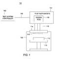
- FIG. 1depicts a test system 100 according to some embodiments of the invention.
- the test system 100can generally include a test system controller 102 , test instruments 104 , a probe card assembly 114 , and a prober 106 .
- the test system controller 102can be coupled to the test instruments 104 by a communication link 108 .
- the test system controller 102may comprise a host computer, for example.
- the prober 106can include a stage 110 for mounting a device under test (DUT) 112 being tested.
- the DUT 112can be any electronic device or devices to be tested.
- Non-limiting examples of a suitable DUTinclude one or more dies of an unsingulated semiconductor wafer, one or more semiconductor dies singulated from a wafer (packaged or unpackaged), an array of singulated semiconductor dies disposed in a carrier or other holding device, one or more multi-die electronics modules, one or more printed circuit boards, or any other type of electronic device or devices.
- the term DUT, as used herein,can refer to one or a plurality of such electronic devices.
- the probe card assembly 114can include probes 116 (also referred to as test probes) that contact the DUT 112 .
- the stage 110can be movable to contact the DUT 112 with probes 116 .
- test signalscan be generated by the test instruments 104 and transmitted through the probe card assembly 114 , the probes 116 , and ultimately to the DUT 112 .
- Overall control of the test instruments 104 for testingmay be orchestrated by the test system controller 102 (e.g., a general purpose computer).
- Test result signalscan then provided from the DUT 112 back through the probe card assembly 114 to the test instruments 104 .
- the test instruments 104may transmit the test result signals to the test system controller 102 for analysis.
- Test data provided from the test instruments 104can be divided into individual test channels.
- the test channelscan be linked by connectors 118 to the probe card assembly 114 .
- the connectors 118may be any suitable connectors, such as flexible cable connectors, pogo pins, zero insertion force (ZIF) connectors, or the like.
- the probe card assembly 114can fan out one or more of the test channels to multiple probes 116 .
- One or more of the test channelscan be coupled to a tester that generates test data and/or processes test result data.
- the test instruments 104can include one or more testers, which may be implemented using one or more integrated circuits (ICs) (“tester ICs 105 ”).
- the probe card assembly 114may include one or more tester ICs 105 alternatively to, or in addition to, the test instruments 104 .
- Each tester IC 105can include dedicated test circuits coupled to programmable logic.
- the programmable logic in a tester IC 105can be responsive to programming data that forms at least one of the dedicated test circuits into a tester for testing the DUT.
- a tester formed by a tester IC 105can generate test data and/or process test result data.
- each tester IC 105can be coupled to at least one of the test channels. Exemplary embodiments of a tester IC 105 are described below.
- FIG. 6depicts the probe card assembly 114 according to some embodiments of the invention.
- the probe card assembly 114generally acts as an interface between the test instruments 104 and the DUT 112 .
- the probe card assembly 114can include electrical connectors 604 configured to make electrical connections with a plurality of test channels from the test instruments 104 .
- the probe card assembly 114can also include one or more resilient contact elements 626 as test probes.
- the resilient contact elements 626can be configured to be pressed against, and thus make temporary electrical connections with, one or more input and/or output terminals 620 of the DUT 112 .
- the resilient contact elements 626are typically configured to correspond to desired terminals 620 of the DUT 112 and may be arranged in one or more arrays having a desired geometry.
- the probe card assembly 114may include one or more substrates configured to support the connectors 604 and the resilient contact elements 626 and to provide electrical connections therebetween.
- the exemplary probe card assembly 114 shown in FIG. 6has three such substrates, although in other implementations, the probe card assembly 114 can have more or fewer substrates.
- the probe card assembly 114includes a wiring substrate 602 (also referred to as a printed wiring board), an interposer substrate 608 , and a probe substrate 624 (also referred to as a probe head).
- the wiring substrate 602 , the interposer substrate 608 , and the probe substrate 624can generally be made of any type of suitable material or materials, such as, without limitation, printed circuit boards, ceramics, organic or inorganic materials, and the like, or combinations thereof.
- the probe card assembly 114may include one or more active or passive electronic components (such as capacitors, resistors, and the like).
- electronics 630can be disposed on the wiring substrate 602 .
- the electronics 630may be used, among other things, to implement tester ICs 105 , as described in embodiments herein.
- the electronics 630may be disposed on the interposer 608 .
- the electronics 630may be disposed on the probe substrate 624 along with the resilient contact elements 626 .
- the electronics 630can be disposed on any combination of one or more of the wiring substrate 602 , the interposer substrate 608 , and the probe substrate 624 .
- Electrically conductive pathsare typically provided from the connectors 604 through the various substrates and the electronics 630 to the resilient contact elements 626 .
- electrically conductive pathsmay be provided from the connectors 604 through the wiring substrate 602 to a plurality of electrically conductive spring interconnect structures 606 .
- Other electrically conductive pathsmay be provided from the spring interconnect structures 606 through the interposer substrate 608 to a plurality of electrically conductive spring interconnect structures 619 .
- Still other electrically conductive pathsmay further be provided from the spring interconnect structures 619 through the probe substrate 624 to the resilient contact elements 626 .
- the electrically conductive paths through the wiring substrate 602 , the interposer substrate 608 , and the probe substrate 624can comprise electrically conductive vias, traces, or the like, that may be disposed on, within, and/or through the wiring substrate 602 , the interposer substrate 608 , and the probe substrate 624 .
- the electronics 630can be provided on one or more of the wiring substrate 602 , the interposer substrate 608 , and/or the probe substrate 624 in the path of at least some of the aforementioned electrically conductive paths, as described in embodiments below.
- the wiring substrate 602 , the interposer substrate 608 , and the probe substrate 624may be held together by one or more brackets 622 and/or other suitable devices (such as by bolts, screws, or other suitable fasteners).
- the configuration of the probe card assembly 114 shown in FIG. 6is exemplary only and is simplified for ease of illustration and discussion and many variations, modifications, and additions are contemplated.
- a probe card assemblymay have fewer or more substrates (e.g., 602 , 608 , 624 ) than the probe card assembly 114 shown in FIG. 6 .
- a probe card assemblymay have more than one probe substrate (e.g., 624 ), and each such probe substrate may be independently adjustable.
- Non-limiting examples of probe card assemblies with multiple probe substratesare disclosed in U.S. patent application Ser. No. 11/165,833, filed Jun. 24, 2005. Additional non-limiting examples of probe card assemblies are illustrated in U.S. Pat. No. 5,974,662, issued Nov. 2, 1999 and U.S. Pat. No. 6,509,751, issued Jan. 21, 2003, as well as in the aforementioned U.S. patent application Ser. No. 11/165,833. It is contemplated that various features of the probe card assemblies described in those patents and application may be implemented in the probe card assembly 114 shown in FIG. 6 and that the probe card assemblies described in the aforementioned patents and application may benefit from the use of the inventive test logic and its configurations described herein.
- FIG. 2is a block diagram depicting a tester IC 105 according to some embodiments of the invention.
- the tester IC 105can include a plurality of dedicated test circuits 202 coupled to a programmable interconnect fabric 204 .
- the dedicated test circuits 202can be used to generate test signals for application to the DUT 112 and/or process test result signals received from the DUT 112 .
- Each of the dedicated test circuits 202can be defined in one or more layers (not shown) of the tester IC 105 during fabrication using photolithographic mask(s).
- Each of the dedicated test circuits 202can include one or more ports 203 each of which is configured to provide output signals, receive input signals, or both.
- the programmable interconnect fabric 204can include input/output (IO) ports 205 that can be programmatically connected to one another via a network of conductor segments 208 and programmable switches 210 .
- the programmable interconnect fabric 204can include a configuration memory 206 .
- the configuration memory 206can include configuration data for establishing connections between specific ones of the IO ports 205 by configuring the programmable switches 210 to connect IO ports 205 with conductor segments 208 and/or conductor segments 208 with other conductor segments 208 .
- At least a portion of the ports 203 of each of the dedicated test circuits 202can be coupled to respective IO ports 205 of the programmable interconnect fabric 204 .
- the tester IC 105can include pins 214 , at least some of which are configured to provide output signals to test channels, receive input signals from test channels, or both.
- the pins 214can be coupled to respective IO ports 205 of the programmable fabric 204 .
- the pins 214can be coupled to bus interface logic 225 in the tester IC 105 , which is in turn coupled to respective IO ports 205 of the programmable interconnect fabric 204 .
- the bus interface logic 225can be used as an interface between a particular type of bus provided externally to the tester IC and the particular IO port configuration of the programmable interconnect fabric 204 .
- the dedicated test circuits 202can be accessed via the programmable interconnect fabric 204 and the pins 214 (optionally through the bus interface logic 225 ). In some embodiments, at least a portion of the ports 203 of the dedicated test circuits 202 can be coupled to respective ones of the pins 214 directly without traversing the programmable interconnect fabric 204 .
- the tester IC 105can include a configuration port 212 for loading configuration data to the configuration memory 206 .
- configuration datacan be loaded to the configuration memory 206 via the configuration port 212 , where the configuration data is designed to couple dedicated test circuit(s) 202 with other dedicated test circuit(s) 202 and/or dedicated test circuit(s) with pin(s) 214 .
- the configuration datamay be designed such that some dedicated test circuit(s) 202 and/or pin(s) 214 are not coupled to any other components (circuits and/or pins) that are being utilized.
- those dedicated test circuits 202 and/or pins 214 that are not necessary for a given test applicationcan be effectively isolated from those dedicated test circuits 202 and/or pins 214 that are required. This can minimize or eliminate any interference caused by unused test circuits 202 and/or pins 214 .
- Various configurations of tester logiccan be implemented to test DUTs across multiple test applications using the dedicated test circuits 202 as “building blocks”.
- the dedicated test circuits 202can include multiple types of test circuits.
- test circuits that can be implemented as the dedicated test circuits 202include timing generators and/or timing counters, formatters, DUT interfaces (e.g., memory interfaces, processor interfaces, system on chip (SoC) interfaces, and the like), IO circuits (e.g., drivers, comparators, etc.), and algorithmic pattern generators (APGs).
- DUT interfacese.g., memory interfaces, processor interfaces, system on chip (SoC) interfaces, and the like
- IO circuitse.g., drivers, comparators, etc.
- APGsalgorithmic pattern generators
- Various other types of circuits that can be used to test a DUTcan be implemented as one or more of the dedicated test circuits 202 .
- the dedicated test circuits 202can include multiple versions of a specific type of test circuit.
- the dedicated test circuits 202can include multiple versions of an IO circuit for communicating with a DUT, each designed to handle a different voltage.
- the dedicated test circuits 202can include multiple versions of an APG, each designed to generate test patterns for different DUTs.
- the specific attribute or attributes that differ among the multiple versions of a specific test circuitare hard-wired (dedicated) within the test circuit.
- one or more of the dedicated test circuits 202can be programmable.
- one or more of the ports 203 of a particular test circuit 202can be control ports configured to receive control signals that can program one or more attributes thereof.
- the dedicated test circuits 202can include an IO circuit for communicating with a DUT, where the IO voltage of the IO circuit can be programmed during testing (e.g., the IO voltage can be selected from a plurality of possible IO voltages).
- the dedicated test circuits 202can include an APG that can be programmed to produce different test patterns potentially across different types of DUTs.
- Various other types of test circuitscan be implemented in the dedicated test circuits 202 to have one or more programmable attributes.
- the tester IC 105can include a processor 250 .
- the processor 250can be a microprocessor, microcontroller, instruction-set processor, or like type device.
- the processor 250can have at least one bus interface 252 . At least a portion of the bus interface(s) 252 can be coupled to IO ports 205 of the programmable interconnect fabric 204 . In some embodiments, at least a portion of the bus interface(s) 252 can be coupled to the pins 214 of the tester IC 105 (without traversing the programmable interconnect fabric 204 ).
- the processor 250can be used to facilitate programming of the configuration memory 206 with configuration data. For example, the processor 250 can load or otherwise control loading of configuration data into the configuration memory 206 .
- the processor 250can dynamically load a portion of the configuration memory 206 with different configuration data while the tester IC is active (dynamic re-programming of the programmable interconnect fabric 204 ). In this manner, different ones of the dedicated test circuits 202 can be incorporated and/or unincorporated into the tester logic dynamically during the testing process.
- the processor 250can operate according to instructions that can be stored in memory within the processor 250 (e.g., cache memory).
- the tester IC 105can include a memory 254 that can be coupled to the processor 250 directly, or coupled to the programmable interconnect fabric 204 (which can be programmed to couple the memory 254 to the processor 250 ).
- the memory 254can store instructions to be executed by the processor 250 . In some embodiments, the memory 254 can store any other data and can be accessed by other circuits through the programmable interconnect fabric 204 , such as the dedicated test circuits 202 .
- the tester IC 105can exhibit advantages over an ASIC tester IC or an FPGA tester IC.
- the tester IC 105includes a programmable interconnect fabric, which allows for specific configurations of dedicated test circuits to be constructed (and reconstructed), in some embodiments dynamically, for particular test applications. In contrast, an ASIC tester IC is hard-wired at the time of fabrication and the configuration of any test circuits therein cannot be changed.
- the tester IC 105also includes a plurality of dedicated test circuits, which can be more efficient (e.g., in terms of area, speed, power consumption, etc.) than equivalent circuits configured in the general purpose programmable logic of an FPGA.
- the dedicated test circuits in the tester IC 105can include some test circuits that are difficult, impracticable, or impossible to implement using the general purpose programmable logic of an FPGA.
- FIG. 3is a block diagram depicting a tester IC 105 according to some additional embodiments of the invention.
- the tester IC 105can include a plurality of dedicated test circuits 302 coupled to a processor 304 .
- the dedicated test circuits 302can be used to generate test signals for application to the DUT 112 and/or process test result signals received from the DUT 112 .
- Each of the dedicated test circuits 302can be defined in one or more layers (not shown) of the tester IC 105 during fabrication using photolithographic mask(s).
- Each of the dedicated test circuits 302can include one or more ports 303 each of which is configured to provide output signals, receive input signals, or both.
- the processor 304can be a microprocessor, microcontroller, instruction-set processor, or like type device.
- the processor 304can have at least one bus interface 305 . At least a portion of the ports 303 of each of the dedicated test circuits 302 can be coupled to the bus interface(s) 305 .
- the processor 304can include a memory 308 .
- the memory 308can store instructions and/or data used by the processor 304 (e.g., cache memory).
- the test IC 105can include a memory 310 external to the processor 304 .
- the memory 310can be coupled to the bus interface(s) 305 of the processor 304 .
- the memory 310can be used to store instructions and/or data for the processor 304 .
- the memory 310can store any other data and can be accessed by other circuits through the processor 304 , such as the dedicated test circuits 302 .
- the tester IC 105can include pins 314 , at least some of which are configured to provide output signals to test channels, receive input signals from test channels, or both. In some embodiments, at least a portion of the ports 303 of the dedicated test circuits 302 can be coupled to respective ones of the pins 314 . In some embodiments, the pins 314 can be coupled to the bus interface(s) 305 of the processor 304 . In other embodiments, the pins 314 can be coupled to bus interface logic 325 in the tester IC 105 , which is in turn coupled to the bus interface(s) 305 of the processor 304 .
- the bus interface logic 325can be used as an interface between a particular type of bus provided externally to the tester IC and the particular bus interface(s) 305 of the processor 304 . If present, the memory 310 can be coupled to the pins 314 either directly or through the bus interface logic 304 . Instructions and/or data can be loaded to the memory 308 and/or the memory 310 through the pins 314 (optionally through the bus interface logic 325 ).
- Instructions and/or datacan be loaded into the memory 308 and/or the memory 310 , where the instructions and/or data is/are designed to cause the processor to select one or more of the dedicated test circuits 302 for implementing tester logic.
- the dedicated test circuits 302may be initially inactive or otherwise unavailable for use.
- the processor 305can execute instructions to activate or otherwise make available for use specific ones of the dedicated test circuits 302 to implement the tester logic. Communication between dedicated test circuits 302 can be handled by the processor 304 . Once active or otherwise made available for use, the dedicated test circuits 302 can communicate with the test channels either directly via the pins 314 , or indirectly through the processor 304 .
- the instructions and/or data used by the processor 305can be designed such that some dedicated test circuit(s) 302 remain inactive or otherwise unavailable for use. In this manner, those dedicated test circuits 302 that are not necessary for a given test application can be effectively isolated from those test circuits 302 that are required. This can minimize or eliminate any interference caused by unused dedicated test circuits 302 .
- Various configurations of tester logiccan be implemented to test DUTs across multiple test applications using the dedicated test circuits 302 as “building blocks”.
- the dedicated test circuits 302can include multiple types of test circuits.
- test circuitsthat can be implemented as the dedicated test circuits 302 include timing generators and/or timing counters, formatters, DUT interfaces (e.g., memory interfaces, processor interfaces, system on chip (SoC) interfaces, and the like), IO circuits (e.g., drivers, comparators, etc.), and algorithmic pattern generators (APGs).
- DUT interfacese.g., memory interfaces, processor interfaces, system on chip (SoC) interfaces, and the like
- IO circuitse.g., drivers, comparators, etc.
- APGsalgorithmic pattern generators
- Various other types of circuits that can be used to test a DUTcan be implemented as one or more of the dedicated test circuits 302 .
- the dedicated test circuits 302can include multiple versions of a specific type of test circuit.
- the dedicated test circuits 302can include multiple versions of an IO circuit for communicating with a DUT, each designed to handle a different voltage.
- the dedicated test circuits 302can include multiple versions of an APG, each designed to generate test patterns for different DUTs.
- the specific attribute or attributes that differ among the multiple versions of a specific test circuitare hard-wired (dedicated) within the test circuit.
- one or more of the dedicated test circuits 302can be programmable.
- the processor 305via instructions and/or data, can control or otherwise program one or more attributes thereof.
- the dedicated test circuits 302can include an IO circuit for communicating with a DUT, where the IO voltage of the IO circuit can be programmed during testing (e.g., the IO voltage can be selected from a plurality of possible IO voltages).
- the dedicated test circuits 302can include an APG that can be programmed to produce different test patterns potentially across different types of DUTs.
- Various other types of test circuitscan be implemented in the dedicated test circuits 302 to have one or more programmable attributes.
- the instructions and/or data stored in the memory 308 and/or the memory 310can be designed such that specific ones of the dedicated test circuits 302 become active/usable and inactive/unusable dynamically while the tester IC 105 is active (e.g., during testing). Thus, different ones of the dedicated test circuits 302 can be incorporated and/or unincorporated into the tester logic dynamically during the testing process.
- the tester IC 105can exhibit advantages over an ASIC tester IC or an FPGA tester IC.
- the tester IC 105includes a programmable processor, which allows for specific configurations of dedicated test circuits to be selected (and reselected), in some embodiments dynamically, for particular test applications. In contrast, an ASIC tester IC is hard-wired at the time of fabrication and the configuration of any test circuits therein cannot be changed.
- the tester IC 105also includes a plurality of dedicated test circuits, which can be more efficient (e.g., in terms of area, speed, power consumption, etc.) that equivalent circuits configured in the general purpose programmable logic of an FPGA.
- the dedicated test circuits in the tester IC 105can include some test circuits that are difficult, impracticable, or impossible to implement using the general purpose programmable logic of an FPGA.
- FIG. 4is a block diagram depicting a test system 400 according to some embodiments of the invention.
- the test system 400can include a tester 450 coupled to test probes 116 .
- the test probes 116can be configured to contact pads 452 on the DUT 112 .
- the tester 450can be implemented using components within a tester IC 105 . Exemplary non-limiting embodiments of a tester IC 105 are shown above with respect to FIGS. 2 and 3 . More generalized embodiments of the tester IC 105 are shown in FIG. 4 .
- the tester IC 105can include a plurality of dedicated test circuits 402 , programmable logic 404 , and an external interface 408 .
- the dedicated test circuits 402can be used to generate test signals for application to the DUT 112 and/or process test result signals received from the DUT 112 .
- Each of the dedicated test circuits 402can be defined in one or more layers (not shown) of the tester IC 105 during fabrication using photolithographic mask(s).
- Each of the dedicated test circuits 402can include one or more ports 403 each of which is configured to provide output signals, receive input signals, or both.
- the programmable logic 404can include an interface 405 . At least a portion of the ports 403 of each of the dedicated test circuits 402 can be coupled to the interface 405 of the programmable logic 404 .
- the programmable logic 404can be responsive to programming data to select one or more of the dedicated test circuits 402 for implementation of the tester 450 .
- the interface 405 of the programmable logic 404can be further coupled to the external interface 408 .
- the external interface 408can include pins of the tester IC 105 . In other embodiments, the external interface 408 can include bus interface logic and pins of the tester IC 105 .
- the dedicated test circuits 402can also be coupled directly to the external interface 408 .
- the external interface 408can provide an interface between the programmable logic 404 and test channels 430 .
- the test channels 430may be implemented on the probe card assembly 114 using signal paths, as described above.
- the external interface 408can be coupled to input terminals 435 of the test channels 430 .
- the test channels 430can be coupled to the test probes 116 .
- the test probes 116can contact the pads 452 of the DUT 112 , allowing the tester 450 to provide test signals to, and receive test result signals from, the DUT 112 .
- the programmable logic 404can include logic capable of being programmed to select one or more of the dedicated test circuits 402 responsive to the programming data.
- the programming datamay be provided to the programmable logic 404 via the external interface 408 and the interface 405 . If a given dedicated test circuit 402 is selected by the programmable logic 404 , such dedicated test circuit 402 becomes part of the implementation of the tester 450 and is capable of performing its function.
- the programmable logic 404can include a programmable interconnect fabric capable of being configured to connect one or more of the dedicated test circuits 402 to each other and/or to the external interface 408 .
- the programming datacan comprise configuration data to be stored in configuration memory of the programmable interconnect fabric.
- the programmable logic 404can include a processor capable of selecting one or more of the dedicated test circuits 402 to be active or otherwise capable of being used.
- the programming datacan comprise instructions and/or data stored in a memory for execution and/or processing by the processor.
- the programmable logic 404can include a combination of a programmable interconnect fabric and a processor.
- the programmable logic 404can include other types of logic in place of or in addition to the programmable interconnect fabric and/or the processor, such other logic being designed to implement the functionality of the programmable logic as described above.
- FIG. 5is a flow diagram depicting a method 500 of testing a device under test according to some embodiments of the invention.
- Programming datacan be loaded into programmable logic of a tester IC ( 502 ).
- the programming datacan program the programmable logic to form a tester from at least one of a plurality of dedicated test circuits in the tester IC.
- the programmable logiccan include a programmable interconnect fabric and the programming data can include configuration data to be loaded into configuration memory of the programmable interconnect fabric.
- the configuration datacan program the programmable interconnect fabric to select one or more of the dedicated test circuits for implementing the tester.
- the programmable logiccan include a processor and the programming data can include instructions and/or data to be executed and/or processed by the processor.
- the instructions and/or datacan cause the processor to select one or more of the dedicated test circuits for implementing the tester.
- the testercan be controlled to generate a test signal for testing the DUT and/or processing a test result signal produced by the DUT ( 504 ).
- the programmable logiccan be actively reprogrammed to reform the tester from the dedicated test circuits ( 506 ).
- the reprogrammingcan be “active” in that the reprogramming can occur while the tester IC is active and in the process or testing the DUT.
- the configuration datacan be at least partially updated to dynamically reconfigure the programmable interconnect fabric to modify the selection of the dedicated test circuits (e.g., different test circuits can be selected and other test circuits can be unselected).
- the instructions and/or datacan be configured to cause the processor to select new dedicated test circuits and/or unselect dedicated test circuits for the tester implementation.
- the method 500can return to controlling the tester to produce test signals and/or processing test result signals given the reprogrammed tester implementation ( 504 ).
- the process of controlling the tester and reprogramming the testercan be repeated one or more times until testing is complete.
Landscapes
- Physics & Mathematics (AREA)
- General Physics & Mathematics (AREA)
- Tests Of Electronic Circuits (AREA)
Abstract
Description
- 1. Field of the Invention
- Embodiments of the present invention relate to semiconductor testing.
- 2. Description of the Related Art
- Testing is an important step in the production of semiconductor devices for use. Typically, partially or fully completed semiconductor devices may be tested by bringing terminals disposed on an upper surface of a device to be tested—also referred to as a device under test (or DUT)—into contact with resilient contact elements, for example, as contained in a probe card assembly, as part of a test system. A test system controller may be coupled to the probe card assembly to send and receive test signals to and from the DUTs over a set of test channels. A test system controller with increased test channels can be a significant cost factor for a test system. Test system controllers have evolved to increase the number of channels and hence the number of devices that can be tested in parallel (sometimes referred to as multi-site testing).
- During testing, some test channels provide test input signals to input pins of the DUTs, others test channels monitor for test result signals from output pins of the DUTs, and still others provide test input signals to, and monitor for test result signals from, input/output (IO) pins of the DUTs. Tester logic can be coupled to the test channels for generating the test input signals and/or processing the test result signals. The tester logic can be part of the test system controller. Some tester logic can include more test circuits than are required for any one test application. Test circuits that are not used in a given test application are nevertheless present and can interfere with the intended operation of test equipment. Other tester logic, while programmable, can make implementation of certain types of test circuits inefficient, impracticable, or even impossible.
- Accordingly, there exists a need in the art for a method and apparatus for testing semiconductor devices that attempts to overcome at least some of the aforementioned deficiencies.
- Embodiments of the invention can relate to an apparatus for testing a semiconductor device under test (DUT). In some embodiments, the apparatus can include an integrated circuit (IC) coupled to test probes configured to contact pads on the DUT, the IC including a plurality of dedicated test circuits coupled to programmable logic, the programmable logic responsive to programming data to form a tester for testing the DUT from at least one of the dedicated test circuits.
- Embodiments of the invention can relate to an apparatus for testing a semiconductor DUT. In some embodiments, the apparatus can include a probe card assembly having input terminals coupled to test probes via signal paths, the test probes configured to contact pads on the DUT; and test instruments, coupled to the input terminals, the test instruments including at least one tester IC, each of the at least one tester IC coupled to one or more of the input terminals and including: a plurality of dedicated test circuits coupled to programmable logic, the programmable logic responsive to programming data to form a tester for testing the DUT from at least one of the dedicated test circuits.
- Embodiments of the invention can relate to a method for testing a semiconductor DUT. In some embodiments, the method can include loading programming data into programmable logic of a tester integrated circuit (IC), the programming data configuring the programmable logic to form a tester from at least one of a plurality of dedicated test circuits in the tester IC; and controlling the tester to perform at least one of: generating a test signal for testing the DUT or processing a test result signal produced by the DUT.
- Embodiments of the invention can relate to a probe card assembly. In some embodiments, the probe card assembly can include signal paths coupled to test probes, the test probes configured to contact pads on a semiconductor device under test (DUT); and at least one tester integrated circuit (IC) coupled one or more of the signal paths and including: a plurality of dedicated test circuits coupled to programmable logic, the programmable logic responsive to programming data to form a tester for testing the DUT from at least one of the dedicated test circuits.
- So that the manner in which features of the various embodiments of the present invention can be understood in detail, a more particular description of the invention, briefly summarized above and described more fully below, may be had by reference to embodiments, some of which are illustrated in the appended drawings. It is to be noted, however, that the appended drawings illustrate only typical embodiments of this invention and are therefore not to be considered limiting of its scope, for the invention may admit to other equally effective embodiments.
FIG. 1 depicts a test system according to some embodiments of the invention;FIG. 2 is a block diagram depicting a tester IC according to some embodiments of the invention;FIG. 3 is a block diagram depicting a tester IC according to some additional embodiments of the invention;FIG. 4 is a block diagram depicting a test system according to some embodiments of the invention;FIG. 5 is a flow diagram depicting a method of testing a device under test according to some embodiments of the invention; andFIG. 6 depicts a probe card assembly according to some embodiments of the invention- Where possible, identical reference numerals are used herein to designate identical elements that are common to the figures. The images used in the drawings are simplified for illustrative purposes and are not necessarily depicted to scale.
- This specification describes exemplary embodiments and applications of the invention. The invention, however, is not limited to these exemplary embodiments and applications or to the manner in which the exemplary embodiments and applications operate or are described herein. Moreover, the Figures may show simplified or partial views, and the dimensions of elements in the Figures may be exaggerated or otherwise not in proportion for clarity. In addition, as the terms “on” and “attached to” are used herein, one object (e.g., a material, a layer, a substrate, etc.) can be “on” or “attached to” another object regardless of whether the one object is directly on or attached to the other object or there are one or more intervening objects between the one object and the other object. Also, directions (e.g., above, below, top, bottom, side, up, down, “x,” “y,” “z,” etc.), if provided, are relative and provided solely by way of example and for ease of illustration and discussion and not by way of limitation. In addition, where reference is made to a list of elements (e.g., elements a, b, c), such reference is intended to include any one of the listed elements by itself, any combination of less than all of the listed elements, and/or a combination of all of the listed elements.
- The present invention provides a method and apparatus for providing a tester integrated circuit (IC) for testing a semiconductor device under test (DUT). A tester IC can be implemented using an application specific integrated circuit (ASIC). In an ASIC, tester logic can be defined in one or more layers during fabrication using a set of photolithographic masks. Such tester logic can be referred to as “dedicated” or “hard-wired”, since the implementation of the tester logic cannot be changed after fabrication. The ASIC may include various types of test circuits for generating and/or processing signals. The ASIC can be designed to be general enough to be used in different types of test applications, including different types of test equipment and different types of DUTs. Thus, the ASIC can include more test circuits than are required for use in any one test application. Test circuits in an ASIC that are not used in a given test application are nevertheless present and can interfere with the intended operation of the test equipment. Moreover, as noted above, an ASIC is hard-wired and the implementation of the test circuits therein cannot be changed once fabricated.
- The tester IC can also be implemented using a programmable logic device (PLD), such as a field programmable gate array (FPGA). An FPGA is an integrated circuit (IC) that include programmable logic blocks and programmable interconnects, each of which can be programmed and reprogrammed after manufacture of the device to implement various logical functions. In a test system, an FPGA can be programmed and reprogrammed with different test circuits for driving the test channels. FPGAs, however, are designed to be general in order to be capable of implementing many different types of circuits across many different applications. The general design of an FPGA can make implementation of certain types of test circuits inefficient, impracticable, or even impossible. Furthermore, test circuits implemented in an FPGA may be slower, require more chip area, and/or consume more power as compared to test circuits implemented using an ASIC.
- Aspects of the invention can relate to an IC coupled to test probes for contacting the DUT. A tester IC can include a plurality of dedicated test circuits coupled to programmable logic. The dedicated test circuits can be “dedicated” in that the circuits can be formed in one or more layers of the IC using photolithography and like type processes during fabrication. The programmable logic can responsive to programming data to form a tester for testing the DUT from at least one of the dedicated test circuits. The tester IC can be more versatile than a pure ASIC, as various implementations of a tester can be formed dedicated test circuits depending on test application. Moreover, dedicated test circuits that are not needed for a particular test application can be isolated from the tester implementation so as to not deleteriously affect tester operation. The tester IC can be more versatile than a pure FPGA, as some dedicated test circuits can be formed more efficiently in terms of area, speed, and power consumption than implementing such circuits using the general purpose programmable blocks of an FPGA. Moreover, the tester IC can include some test circuits that are difficult, impracticable, or impossible to form using the general purpose programmable blocks of an FPGA.
FIG. 1 depicts atest system 100 according to some embodiments of the invention. Thetest system 100 can generally include atest system controller 102,test instruments 104, aprobe card assembly 114, and aprober 106. Thetest system controller 102 can be coupled to thetest instruments 104 by acommunication link 108. Thetest system controller 102 may comprise a host computer, for example. Theprober 106 can include astage 110 for mounting a device under test (DUT)112 being tested. TheDUT 112 can be any electronic device or devices to be tested. Non-limiting examples of a suitable DUT include one or more dies of an unsingulated semiconductor wafer, one or more semiconductor dies singulated from a wafer (packaged or unpackaged), an array of singulated semiconductor dies disposed in a carrier or other holding device, one or more multi-die electronics modules, one or more printed circuit boards, or any other type of electronic device or devices. The term DUT, as used herein, can refer to one or a plurality of such electronic devices. Theprobe card assembly 114 can include probes116 (also referred to as test probes) that contact theDUT 112. Thestage 110 can be movable to contact theDUT 112 withprobes 116.- In the
test system 100, test signals can be generated by thetest instruments 104 and transmitted through theprobe card assembly 114, theprobes 116, and ultimately to theDUT 112. Overall control of thetest instruments 104 for testing may be orchestrated by the test system controller102 (e.g., a general purpose computer). Test result signals can then provided from theDUT 112 back through theprobe card assembly 114 to thetest instruments 104. Thetest instruments 104 may transmit the test result signals to thetest system controller 102 for analysis. - Test data provided from the
test instruments 104 can be divided into individual test channels. The test channels can be linked byconnectors 118 to theprobe card assembly 114. Theconnectors 118 may be any suitable connectors, such as flexible cable connectors, pogo pins, zero insertion force (ZIF) connectors, or the like. Theprobe card assembly 114 can fan out one or more of the test channels tomultiple probes 116. One or more of the test channels can be coupled to a tester that generates test data and/or processes test result data. In some embodiments, thetest instruments 104 can include one or more testers, which may be implemented using one or more integrated circuits (ICs) (“tester ICs 105”). In some embodiments, theprobe card assembly 114 may include one ormore tester ICs 105 alternatively to, or in addition to, thetest instruments 104. - Each
tester IC 105 can include dedicated test circuits coupled to programmable logic. The programmable logic in atester IC 105 can be responsive to programming data that forms at least one of the dedicated test circuits into a tester for testing the DUT. A tester formed by atester IC 105 can generate test data and/or process test result data. Thus, eachtester IC 105 can be coupled to at least one of the test channels. Exemplary embodiments of atester IC 105 are described below. FIG. 6 depicts theprobe card assembly 114 according to some embodiments of the invention. Theprobe card assembly 114 generally acts as an interface between thetest instruments 104 and theDUT 112. Theprobe card assembly 114 can includeelectrical connectors 604 configured to make electrical connections with a plurality of test channels from thetest instruments 104. Theprobe card assembly 114 can also include one or moreresilient contact elements 626 as test probes. Theresilient contact elements 626 can be configured to be pressed against, and thus make temporary electrical connections with, one or more input and/oroutput terminals 620 of theDUT 112. Theresilient contact elements 626 are typically configured to correspond to desiredterminals 620 of theDUT 112 and may be arranged in one or more arrays having a desired geometry.- The
probe card assembly 114 may include one or more substrates configured to support theconnectors 604 and theresilient contact elements 626 and to provide electrical connections therebetween. The exemplaryprobe card assembly 114 shown inFIG. 6 has three such substrates, although in other implementations, theprobe card assembly 114 can have more or fewer substrates. In the embodiment depicted inFIG. 6 , theprobe card assembly 114 includes a wiring substrate602 (also referred to as a printed wiring board), aninterposer substrate 608, and a probe substrate624 (also referred to as a probe head). Thewiring substrate 602, theinterposer substrate 608, and theprobe substrate 624 can generally be made of any type of suitable material or materials, such as, without limitation, printed circuit boards, ceramics, organic or inorganic materials, and the like, or combinations thereof. - Additionally, the
probe card assembly 114 may include one or more active or passive electronic components (such as capacitors, resistors, and the like). In some embodiments,electronics 630 can be disposed on thewiring substrate 602. Theelectronics 630 may be used, among other things, to implementtester ICs 105, as described in embodiments herein. In other embodiments, theelectronics 630 may be disposed on theinterposer 608. In still other embodiments, theelectronics 630 may be disposed on theprobe substrate 624 along with theresilient contact elements 626. In other embodiments, theelectronics 630 can be disposed on any combination of one or more of thewiring substrate 602, theinterposer substrate 608, and theprobe substrate 624. - Electrically conductive paths (examples shown below) are typically provided from the
connectors 604 through the various substrates and theelectronics 630 to theresilient contact elements 626. For example, in the embodiment depicted inFIG. 6 , electrically conductive paths may be provided from theconnectors 604 through thewiring substrate 602 to a plurality of electrically conductivespring interconnect structures 606. Other electrically conductive paths may be provided from thespring interconnect structures 606 through theinterposer substrate 608 to a plurality of electrically conductivespring interconnect structures 619. Still other electrically conductive paths may further be provided from thespring interconnect structures 619 through theprobe substrate 624 to theresilient contact elements 626. The electrically conductive paths through thewiring substrate 602, theinterposer substrate 608, and theprobe substrate 624 can comprise electrically conductive vias, traces, or the like, that may be disposed on, within, and/or through thewiring substrate 602, theinterposer substrate 608, and theprobe substrate 624. Theelectronics 630 can be provided on one or more of thewiring substrate 602, theinterposer substrate 608, and/or theprobe substrate 624 in the path of at least some of the aforementioned electrically conductive paths, as described in embodiments below. - The
wiring substrate 602, theinterposer substrate 608, and theprobe substrate 624 may be held together by one ormore brackets 622 and/or other suitable devices (such as by bolts, screws, or other suitable fasteners). The configuration of theprobe card assembly 114 shown inFIG. 6 is exemplary only and is simplified for ease of illustration and discussion and many variations, modifications, and additions are contemplated. For example, a probe card assembly may have fewer or more substrates (e.g.,602,608,624) than theprobe card assembly 114 shown inFIG. 6 . As another example, a probe card assembly may have more than one probe substrate (e.g.,624), and each such probe substrate may be independently adjustable. Non-limiting examples of probe card assemblies with multiple probe substrates are disclosed in U.S. patent application Ser. No. 11/165,833, filed Jun. 24, 2005. Additional non-limiting examples of probe card assemblies are illustrated in U.S. Pat. No. 5,974,662, issued Nov. 2, 1999 and U.S. Pat. No. 6,509,751, issued Jan. 21, 2003, as well as in the aforementioned U.S. patent application Ser. No. 11/165,833. It is contemplated that various features of the probe card assemblies described in those patents and application may be implemented in theprobe card assembly 114 shown inFIG. 6 and that the probe card assemblies described in the aforementioned patents and application may benefit from the use of the inventive test logic and its configurations described herein. FIG. 2 is a block diagram depicting atester IC 105 according to some embodiments of the invention. Thetester IC 105 can include a plurality ofdedicated test circuits 202 coupled to aprogrammable interconnect fabric 204. Thededicated test circuits 202 can be used to generate test signals for application to theDUT 112 and/or process test result signals received from theDUT 112. Each of thededicated test circuits 202 can be defined in one or more layers (not shown) of thetester IC 105 during fabrication using photolithographic mask(s). Each of thededicated test circuits 202 can include one ormore ports 203 each of which is configured to provide output signals, receive input signals, or both.- The
programmable interconnect fabric 204 can include input/output (IO)ports 205 that can be programmatically connected to one another via a network ofconductor segments 208 andprogrammable switches 210. Theprogrammable interconnect fabric 204 can include aconfiguration memory 206. Theconfiguration memory 206 can include configuration data for establishing connections between specific ones of theIO ports 205 by configuring theprogrammable switches 210 to connectIO ports 205 withconductor segments 208 and/orconductor segments 208 withother conductor segments 208. At least a portion of theports 203 of each of thededicated test circuits 202 can be coupled torespective IO ports 205 of theprogrammable interconnect fabric 204. - The
tester IC 105 can includepins 214, at least some of which are configured to provide output signals to test channels, receive input signals from test channels, or both. In some embodiments, thepins 214 can be coupled torespective IO ports 205 of theprogrammable fabric 204. In other embodiments, thepins 214 can be coupled tobus interface logic 225 in thetester IC 105, which is in turn coupled torespective IO ports 205 of theprogrammable interconnect fabric 204. Thebus interface logic 225 can be used as an interface between a particular type of bus provided externally to the tester IC and the particular IO port configuration of theprogrammable interconnect fabric 204. Thededicated test circuits 202 can be accessed via theprogrammable interconnect fabric 204 and the pins214 (optionally through the bus interface logic225). In some embodiments, at least a portion of theports 203 of thededicated test circuits 202 can be coupled to respective ones of thepins 214 directly without traversing theprogrammable interconnect fabric 204. - The
tester IC 105 can include aconfiguration port 212 for loading configuration data to theconfiguration memory 206. To implement tester logic, configuration data can be loaded to theconfiguration memory 206 via theconfiguration port 212, where the configuration data is designed to couple dedicated test circuit(s)202 with other dedicated test circuit(s)202 and/or dedicated test circuit(s) with pin(s)214. The configuration data may be designed such that some dedicated test circuit(s)202 and/or pin(s)214 are not coupled to any other components (circuits and/or pins) that are being utilized. In this manner, those dedicatedtest circuits 202 and/or pins214 that are not necessary for a given test application can be effectively isolated from those dedicatedtest circuits 202 and/or pins214 that are required. This can minimize or eliminate any interference caused byunused test circuits 202 and/or pins214. Various configurations of tester logic can be implemented to test DUTs across multiple test applications using the dedicatedtest circuits 202 as “building blocks”. - The
dedicated test circuits 202 can include multiple types of test circuits. Non-limiting examples of test circuits that can be implemented as thededicated test circuits 202 include timing generators and/or timing counters, formatters, DUT interfaces (e.g., memory interfaces, processor interfaces, system on chip (SoC) interfaces, and the like), IO circuits (e.g., drivers, comparators, etc.), and algorithmic pattern generators (APGs). Various other types of circuits that can be used to test a DUT can be implemented as one or more of thededicated test circuits 202. - The
dedicated test circuits 202 can include multiple versions of a specific type of test circuit. In a non-limiting example, thededicated test circuits 202 can include multiple versions of an IO circuit for communicating with a DUT, each designed to handle a different voltage. In another non-limiting example, thededicated test circuits 202 can include multiple versions of an APG, each designed to generate test patterns for different DUTs. In such embodiments, the specific attribute or attributes that differ among the multiple versions of a specific test circuit are hard-wired (dedicated) within the test circuit. - In some embodiments, one or more of the
dedicated test circuits 202 can be programmable. For example, one or more of theports 203 of aparticular test circuit 202 can be control ports configured to receive control signals that can program one or more attributes thereof. In a non-limiting example, thededicated test circuits 202 can include an IO circuit for communicating with a DUT, where the IO voltage of the IO circuit can be programmed during testing (e.g., the IO voltage can be selected from a plurality of possible IO voltages). In another non-limiting example, thededicated test circuits 202 can include an APG that can be programmed to produce different test patterns potentially across different types of DUTs. Various other types of test circuits can be implemented in thededicated test circuits 202 to have one or more programmable attributes. - In some embodiments, the
tester IC 105 can include aprocessor 250. Theprocessor 250 can be a microprocessor, microcontroller, instruction-set processor, or like type device. Theprocessor 250 can have at least onebus interface 252. At least a portion of the bus interface(s)252 can be coupled toIO ports 205 of theprogrammable interconnect fabric 204. In some embodiments, at least a portion of the bus interface(s)252 can be coupled to thepins 214 of the tester IC105 (without traversing the programmable interconnect fabric204). In some embodiments, theprocessor 250 can be used to facilitate programming of theconfiguration memory 206 with configuration data. For example, theprocessor 250 can load or otherwise control loading of configuration data into theconfiguration memory 206. Theprocessor 250 can dynamically load a portion of theconfiguration memory 206 with different configuration data while the tester IC is active (dynamic re-programming of the programmable interconnect fabric204). In this manner, different ones of thededicated test circuits 202 can be incorporated and/or unincorporated into the tester logic dynamically during the testing process. Theprocessor 250 can operate according to instructions that can be stored in memory within the processor250 (e.g., cache memory). In some embodiments, thetester IC 105 can include amemory 254 that can be coupled to theprocessor 250 directly, or coupled to the programmable interconnect fabric204 (which can be programmed to couple thememory 254 to the processor250). Thememory 254 can store instructions to be executed by theprocessor 250. In some embodiments, thememory 254 can store any other data and can be accessed by other circuits through theprogrammable interconnect fabric 204, such as thededicated test circuits 202. - The
tester IC 105 can exhibit advantages over an ASIC tester IC or an FPGA tester IC. Thetester IC 105 includes a programmable interconnect fabric, which allows for specific configurations of dedicated test circuits to be constructed (and reconstructed), in some embodiments dynamically, for particular test applications. In contrast, an ASIC tester IC is hard-wired at the time of fabrication and the configuration of any test circuits therein cannot be changed. Thetester IC 105 also includes a plurality of dedicated test circuits, which can be more efficient (e.g., in terms of area, speed, power consumption, etc.) than equivalent circuits configured in the general purpose programmable logic of an FPGA. Moreover, the dedicated test circuits in thetester IC 105 can include some test circuits that are difficult, impracticable, or impossible to implement using the general purpose programmable logic of an FPGA. FIG. 3 is a block diagram depicting atester IC 105 according to some additional embodiments of the invention. Thetester IC 105 can include a plurality ofdedicated test circuits 302 coupled to aprocessor 304. Thededicated test circuits 302 can be used to generate test signals for application to theDUT 112 and/or process test result signals received from theDUT 112. Each of thededicated test circuits 302 can be defined in one or more layers (not shown) of thetester IC 105 during fabrication using photolithographic mask(s). Each of thededicated test circuits 302 can include one ormore ports 303 each of which is configured to provide output signals, receive input signals, or both.- The
processor 304 can be a microprocessor, microcontroller, instruction-set processor, or like type device. Theprocessor 304 can have at least onebus interface 305. At least a portion of theports 303 of each of thededicated test circuits 302 can be coupled to the bus interface(s)305. In some embodiments, theprocessor 304 can include amemory 308. Thememory 308 can store instructions and/or data used by the processor304 (e.g., cache memory). In some embodiments, thetest IC 105 can include amemory 310 external to theprocessor 304. Thememory 310 can be coupled to the bus interface(s)305 of theprocessor 304. Thememory 310 can be used to store instructions and/or data for theprocessor 304. In some embodiments, thememory 310 can store any other data and can be accessed by other circuits through theprocessor 304, such as thededicated test circuits 302. - The
tester IC 105 can includepins 314, at least some of which are configured to provide output signals to test channels, receive input signals from test channels, or both. In some embodiments, at least a portion of theports 303 of thededicated test circuits 302 can be coupled to respective ones of thepins 314. In some embodiments, thepins 314 can be coupled to the bus interface(s)305 of theprocessor 304. In other embodiments, thepins 314 can be coupled tobus interface logic 325 in thetester IC 105, which is in turn coupled to the bus interface(s)305 of theprocessor 304. Thebus interface logic 325 can be used as an interface between a particular type of bus provided externally to the tester IC and the particular bus interface(s)305 of theprocessor 304. If present, thememory 310 can be coupled to thepins 314 either directly or through thebus interface logic 304. Instructions and/or data can be loaded to thememory 308 and/or thememory 310 through the pins314 (optionally through the bus interface logic325). - Instructions and/or data can be loaded into the
memory 308 and/or thememory 310, where the instructions and/or data is/are designed to cause the processor to select one or more of thededicated test circuits 302 for implementing tester logic. For example, thededicated test circuits 302 may be initially inactive or otherwise unavailable for use. Theprocessor 305 can execute instructions to activate or otherwise make available for use specific ones of thededicated test circuits 302 to implement the tester logic. Communication betweendedicated test circuits 302 can be handled by theprocessor 304. Once active or otherwise made available for use, thededicated test circuits 302 can communicate with the test channels either directly via thepins 314, or indirectly through theprocessor 304. The instructions and/or data used by theprocessor 305 can be designed such that some dedicated test circuit(s)302 remain inactive or otherwise unavailable for use. In this manner, those dedicatedtest circuits 302 that are not necessary for a given test application can be effectively isolated from thosetest circuits 302 that are required. This can minimize or eliminate any interference caused by unuseddedicated test circuits 302. Various configurations of tester logic can be implemented to test DUTs across multiple test applications using the dedicatedtest circuits 302 as “building blocks”. - The
dedicated test circuits 302 can include multiple types of test circuits. Non-limiting examples of test circuits that can be implemented as thededicated test circuits 302 include timing generators and/or timing counters, formatters, DUT interfaces (e.g., memory interfaces, processor interfaces, system on chip (SoC) interfaces, and the like), IO circuits (e.g., drivers, comparators, etc.), and algorithmic pattern generators (APGs). Various other types of circuits that can be used to test a DUT can be implemented as one or more of thededicated test circuits 302. - The
dedicated test circuits 302 can include multiple versions of a specific type of test circuit. In a non-limiting example, thededicated test circuits 302 can include multiple versions of an IO circuit for communicating with a DUT, each designed to handle a different voltage. In another non-limiting example, thededicated test circuits 302 can include multiple versions of an APG, each designed to generate test patterns for different DUTs. In such embodiments, the specific attribute or attributes that differ among the multiple versions of a specific test circuit are hard-wired (dedicated) within the test circuit. - In some embodiments, one or more of the
dedicated test circuits 302 can be programmable. For example, theprocessor 305, via instructions and/or data, can control or otherwise program one or more attributes thereof. In a non-limiting example, thededicated test circuits 302 can include an IO circuit for communicating with a DUT, where the IO voltage of the IO circuit can be programmed during testing (e.g., the IO voltage can be selected from a plurality of possible IO voltages). In another non-limiting example, thededicated test circuits 302 can include an APG that can be programmed to produce different test patterns potentially across different types of DUTs. Various other types of test circuits can be implemented in thededicated test circuits 302 to have one or more programmable attributes. - In some embodiments, the instructions and/or data stored in the
memory 308 and/or thememory 310 can be designed such that specific ones of thededicated test circuits 302 become active/usable and inactive/unusable dynamically while thetester IC 105 is active (e.g., during testing). Thus, different ones of thededicated test circuits 302 can be incorporated and/or unincorporated into the tester logic dynamically during the testing process. - The
tester IC 105 can exhibit advantages over an ASIC tester IC or an FPGA tester IC. Thetester IC 105 includes a programmable processor, which allows for specific configurations of dedicated test circuits to be selected (and reselected), in some embodiments dynamically, for particular test applications. In contrast, an ASIC tester IC is hard-wired at the time of fabrication and the configuration of any test circuits therein cannot be changed. Thetester IC 105 also includes a plurality of dedicated test circuits, which can be more efficient (e.g., in terms of area, speed, power consumption, etc.) that equivalent circuits configured in the general purpose programmable logic of an FPGA. Moreover, the dedicated test circuits in thetester IC 105 can include some test circuits that are difficult, impracticable, or impossible to implement using the general purpose programmable logic of an FPGA. FIG. 4 is a block diagram depicting atest system 400 according to some embodiments of the invention. Thetest system 400 can include atester 450 coupled to testprobes 116. The test probes116 can be configured to contactpads 452 on theDUT 112. Thetester 450 can be implemented using components within atester IC 105. Exemplary non-limiting embodiments of atester IC 105 are shown above with respect toFIGS. 2 and 3 . More generalized embodiments of thetester IC 105 are shown inFIG. 4 .- The
tester IC 105 can include a plurality ofdedicated test circuits 402,programmable logic 404, and anexternal interface 408. Thededicated test circuits 402 can be used to generate test signals for application to theDUT 112 and/or process test result signals received from theDUT 112. Each of thededicated test circuits 402 can be defined in one or more layers (not shown) of thetester IC 105 during fabrication using photolithographic mask(s). Each of thededicated test circuits 402 can include one ormore ports 403 each of which is configured to provide output signals, receive input signals, or both. - The
programmable logic 404 can include aninterface 405. At least a portion of theports 403 of each of thededicated test circuits 402 can be coupled to theinterface 405 of theprogrammable logic 404. Theprogrammable logic 404 can be responsive to programming data to select one or more of thededicated test circuits 402 for implementation of thetester 450. Theinterface 405 of theprogrammable logic 404 can be further coupled to theexternal interface 408. In some embodiments, theexternal interface 408 can include pins of thetester IC 105. In other embodiments, theexternal interface 408 can include bus interface logic and pins of thetester IC 105. In some embodiments, thededicated test circuits 402 can also be coupled directly to theexternal interface 408. - The
external interface 408 can provide an interface between theprogrammable logic 404 andtest channels 430. Thetest channels 430 may be implemented on theprobe card assembly 114 using signal paths, as described above. Theexternal interface 408 can be coupled to inputterminals 435 of thetest channels 430. Thetest channels 430 can be coupled to the test probes116. During testing, the test probes116 can contact thepads 452 of theDUT 112, allowing thetester 450 to provide test signals to, and receive test result signals from, theDUT 112. - The
programmable logic 404 can include logic capable of being programmed to select one or more of thededicated test circuits 402 responsive to the programming data. The programming data may be provided to theprogrammable logic 404 via theexternal interface 408 and theinterface 405. If a givendedicated test circuit 402 is selected by theprogrammable logic 404, suchdedicated test circuit 402 becomes part of the implementation of thetester 450 and is capable of performing its function. Some embodiments of theprogrammable logic 404 are described above. For example, in some embodiments, theprogrammable logic 404 can include a programmable interconnect fabric capable of being configured to connect one or more of thededicated test circuits 402 to each other and/or to theexternal interface 408. The programming data can comprise configuration data to be stored in configuration memory of the programmable interconnect fabric. In some embodiments, theprogrammable logic 404 can include a processor capable of selecting one or more of thededicated test circuits 402 to be active or otherwise capable of being used. The programming data can comprise instructions and/or data stored in a memory for execution and/or processing by the processor. In some embodiments, theprogrammable logic 404 can include a combination of a programmable interconnect fabric and a processor. Theprogrammable logic 404 can include other types of logic in place of or in addition to the programmable interconnect fabric and/or the processor, such other logic being designed to implement the functionality of the programmable logic as described above. FIG. 5 is a flow diagram depicting amethod 500 of testing a device under test according to some embodiments of the invention. Programming data can be loaded into programmable logic of a tester IC (502). The programming data can program the programmable logic to form a tester from at least one of a plurality of dedicated test circuits in the tester IC. In some embodiments, the programmable logic can include a programmable interconnect fabric and the programming data can include configuration data to be loaded into configuration memory of the programmable interconnect fabric. The configuration data can program the programmable interconnect fabric to select one or more of the dedicated test circuits for implementing the tester. In other embodiments, the programmable logic can include a processor and the programming data can include instructions and/or data to be executed and/or processed by the processor. The instructions and/or data can cause the processor to select one or more of the dedicated test circuits for implementing the tester.- The tester can be controlled to generate a test signal for testing the DUT and/or processing a test result signal produced by the DUT (504). In some embodiments, the programmable logic can be actively reprogrammed to reform the tester from the dedicated test circuits (506). The reprogramming can be “active” in that the reprogramming can occur while the tester IC is active and in the process or testing the DUT. For example, if the programmable logic includes a programmable interconnect fabric, the configuration data can be at least partially updated to dynamically reconfigure the programmable interconnect fabric to modify the selection of the dedicated test circuits (e.g., different test circuits can be selected and other test circuits can be unselected). If the programmable logic includes a processor, the instructions and/or data can be configured to cause the processor to select new dedicated test circuits and/or unselect dedicated test circuits for the tester implementation. The
method 500 can return to controlling the tester to produce test signals and/or processing test result signals given the reprogrammed tester implementation (504). The process of controlling the tester and reprogramming the tester can be repeated one or more times until testing is complete. - While the foregoing is directed to embodiments of the present invention, other and further embodiments of the invention may be devised without departing from the basic scope thereof, and the scope thereof is determined by the claims that follow.
Claims (27)
Priority Applications (1)
| Application Number | Priority Date | Filing Date | Title |
|---|---|---|---|
| US12/239,326US7944225B2 (en) | 2008-09-26 | 2008-09-26 | Method and apparatus for providing a tester integrated circuit for testing a semiconductor device under test |
Applications Claiming Priority (1)
| Application Number | Priority Date | Filing Date | Title |
|---|---|---|---|
| US12/239,326US7944225B2 (en) | 2008-09-26 | 2008-09-26 | Method and apparatus for providing a tester integrated circuit for testing a semiconductor device under test |
Publications (2)
| Publication Number | Publication Date |
|---|---|
| US20100079159A1true US20100079159A1 (en) | 2010-04-01 |
| US7944225B2 US7944225B2 (en) | 2011-05-17 |
Family
ID=42056729
Family Applications (1)
| Application Number | Title | Priority Date | Filing Date |
|---|---|---|---|
| US12/239,326Active2029-04-22US7944225B2 (en) | 2008-09-26 | 2008-09-26 | Method and apparatus for providing a tester integrated circuit for testing a semiconductor device under test |
Country Status (1)
| Country | Link |
|---|---|
| US (1) | US7944225B2 (en) |
Cited By (19)
| Publication number | Priority date | Publication date | Assignee | Title |
|---|---|---|---|---|
| US20090254296A1 (en)* | 2008-04-08 | 2009-10-08 | Princeton Technology Corporation | Circuit testing apparatus |
| WO2011149725A3 (en)* | 2010-05-28 | 2012-01-26 | Verigy (Singapore) Pte. Ltd. | Flexible storage interface tester with variable parallelism and firmware upgradeability |
| US20160097805A1 (en)* | 2014-10-02 | 2016-04-07 | Xilinx, Inc. | In-die transistor characterization in an ic |
| CN110376509A (en)* | 2019-07-23 | 2019-10-25 | 杭州兴长科技有限公司 | A kind of flexible positioning detection device for integrated circuit |
| US10497630B2 (en)* | 2018-04-05 | 2019-12-03 | Texas Instruments Incorporated | High density wafer level test module |
| JP2020042047A (en)* | 2014-02-07 | 2020-03-19 | 株式会社半導体エネルギー研究所 | Device |
| US10866264B2 (en)* | 2018-01-05 | 2020-12-15 | Intel Corporation | Interconnect structure with varying modulus of elasticity |
| US10877068B2 (en) | 2018-01-05 | 2020-12-29 | Intel Corporation | High density and fine pitch interconnect structures in an electric test apparatus |
| CN112272130A (en)* | 2020-09-25 | 2021-01-26 | 杭州加速科技有限公司 | Communication bus system of semiconductor tester |
| US10935573B2 (en) | 2018-09-28 | 2021-03-02 | Intel Corporation | Slip-plane MEMS probe for high-density and fine pitch interconnects |
| US11061068B2 (en) | 2017-12-05 | 2021-07-13 | Intel Corporation | Multi-member test probe structure |
| US11073538B2 (en) | 2018-01-03 | 2021-07-27 | Intel Corporation | Electrical testing apparatus with lateral movement of a probe support substrate |
| CN113640556A (en)* | 2021-08-11 | 2021-11-12 | 山东大学 | A probe station needle card |
| US11204555B2 (en) | 2017-12-28 | 2021-12-21 | Intel Corporation | Method and apparatus to develop lithographically defined high aspect ratio interconnects |
| US11262384B2 (en) | 2016-12-23 | 2022-03-01 | Intel Corporation | Fine pitch probe card methods and systems |
| US11268983B2 (en) | 2017-06-30 | 2022-03-08 | Intel Corporation | Chevron interconnect for very fine pitch probing |
| US11543454B2 (en) | 2018-09-25 | 2023-01-03 | Intel Corporation | Double-beam test probe |
| US11674980B2 (en) | 2017-09-29 | 2023-06-13 | Intel Corporation | Low-profile gimbal platform for high-resolution in situ co-planarity adjustment |
| US20230184821A1 (en)* | 2021-12-09 | 2023-06-15 | Nanya Technology Corporation | Appratus for performing multiple tests on a device under test |
Families Citing this family (4)
| Publication number | Priority date | Publication date | Assignee | Title |
|---|---|---|---|---|
| US8990633B2 (en)* | 2009-04-21 | 2015-03-24 | Freescale Semiconductor, Inc. | Tracing support for interconnect fabric |
| US9910086B2 (en) | 2012-01-17 | 2018-03-06 | Allen Czamara | Test IP-based A.T.E. instrument architecture |
| KR101913839B1 (en) | 2012-04-10 | 2018-12-31 | 삼성디스플레이 주식회사 | Display device and test method thereof |
| US10162006B2 (en) | 2015-04-16 | 2018-12-25 | Western Digital Technologies, Inc. | Boundary scan testing a storage device via system management bus interface |
Citations (27)
| Publication number | Priority date | Publication date | Assignee | Title |
|---|---|---|---|---|
| US5772451A (en)* | 1993-11-16 | 1998-06-30 | Form Factor, Inc. | Sockets for electronic components and methods of connecting to electronic components |
| US5806181A (en)* | 1993-11-16 | 1998-09-15 | Formfactor, Inc. | Contact carriers (tiles) for populating larger substrates with spring contacts |
| US5821763A (en)* | 1992-10-19 | 1998-10-13 | International Business Machines Corporation | Test probe for high density integrated circuits, methods of fabrication thereof and methods of use thereof |
| US5829128A (en)* | 1993-11-16 | 1998-11-03 | Formfactor, Inc. | Method of mounting resilient contact structures to semiconductor devices |
| US5832601A (en)* | 1993-11-16 | 1998-11-10 | Form Factor, Inc. | Method of making temporary connections between electronic components |
| US5834946A (en)* | 1995-10-19 | 1998-11-10 | Mosaid Technologies Incorporated | Integrated circuit test head |
| US5838163A (en)* | 1992-07-02 | 1998-11-17 | Lsi Logic Corporation | Testing and exercising individual, unsingulated dies on a wafer |
| US5878486A (en)* | 1993-11-16 | 1999-03-09 | Formfactor, Inc. | Method of burning-in semiconductor devices |
| US5897326A (en)* | 1993-11-16 | 1999-04-27 | Eldridge; Benjamin N. | Method of exercising semiconductor devices |
| US5900738A (en)* | 1993-11-16 | 1999-05-04 | Formfactor, Inc. | Contact structure device for interconnections, interposer, semiconductor assembly and package using the same and method |
| US5974662A (en)* | 1993-11-16 | 1999-11-02 | Formfactor, Inc. | Method of planarizing tips of probe elements of a probe card assembly |
| US5983493A (en)* | 1993-11-16 | 1999-11-16 | Formfactor, Inc. | Method of temporarily, then permanently, connecting to a semiconductor device |
| US6029344A (en)* | 1993-11-16 | 2000-02-29 | Formfactor, Inc. | Composite interconnection element for microelectronic components, and method of making same |
| US6059982A (en)* | 1997-09-30 | 2000-05-09 | International Business Machines Corporation | Micro probe assembly and method of fabrication |
| US6064213A (en)* | 1993-11-16 | 2000-05-16 | Formfactor, Inc. | Wafer-level burn-in and test |
| US6110823A (en)* | 1993-11-16 | 2000-08-29 | Formfactor, Inc. | Method of modifying the thickness of a plating on a member by creating a temperature gradient on the member, applications for employing such a method, and structures resulting from such a method |
| US6133744A (en)* | 1995-04-28 | 2000-10-17 | Nec Corporation | Apparatus for testing semiconductor wafer |
| US6174744B1 (en)* | 1995-11-22 | 2001-01-16 | Advantest Corp. | Method of producing micro contact structure and contact probe using same |
| US6219908B1 (en)* | 1991-06-04 | 2001-04-24 | Micron Technology, Inc. | Method and apparatus for manufacturing known good semiconductor die |
| US6275051B1 (en)* | 1997-12-29 | 2001-08-14 | International Business Machines Corporation | Segmented architecture for wafer test and burn-in |
| US6316988B1 (en)* | 1999-03-26 | 2001-11-13 | Seagate Technology Llc | Voltage margin testing using an embedded programmable voltage source |
| US6525555B1 (en)* | 1993-11-16 | 2003-02-25 | Formfactor, Inc. | Wafer-level burn-in and test |
| US6535555B1 (en)* | 1999-04-26 | 2003-03-18 | Thomson Licensing S.A. | Quantizing method and device for video compression |
| US6856150B2 (en)* | 2001-04-10 | 2005-02-15 | Formfactor, Inc. | Probe card with coplanar daughter card |
| US7109736B2 (en)* | 2000-04-13 | 2006-09-19 | Formfactor, Inc. | System for measuring signal path resistance for an integrated circuit tester interconnect structure |
| US7123039B2 (en)* | 2004-08-13 | 2006-10-17 | Jason Gonzalez | Testing input/output voltages in integrated circuits |
| US7307433B2 (en)* | 2004-04-21 | 2007-12-11 | Formfactor, Inc. | Intelligent probe card architecture |
Family Cites Families (59)
| Publication number | Priority date | Publication date | Assignee | Title |
|---|---|---|---|---|
| US3781683A (en) | 1971-03-30 | 1973-12-25 | Ibm | Test circuit configuration for integrated semiconductor circuits and a test system containing said configuration |
| US3827820A (en) | 1971-08-20 | 1974-08-06 | J Hoffman | Drill dispensing container |
| US4038599A (en) | 1974-12-30 | 1977-07-26 | International Business Machines Corporation | High density wafer contacting and test system |
| US4523144A (en) | 1980-05-27 | 1985-06-11 | Japan Electronic Materials Corp. | Complex probe card for testing a semiconductor wafer |
| JPS5951109B2 (en)* | 1980-08-29 | 1984-12-12 | 富士通株式会社 | How to connect high temperature and low temperature parts in aging equipment |
| US4455654B1 (en) | 1981-06-05 | 1991-04-30 | Test apparatus for electronic assemblies employing a microprocessor | |
| US4706018A (en) | 1984-11-01 | 1987-11-10 | International Business Machines Corporation | Noncontact dynamic tester for integrated circuits |
| US4780670A (en) | 1985-03-04 | 1988-10-25 | Xerox Corporation | Active probe card for high resolution/low noise wafer level testing |
| US4837622A (en) | 1985-05-10 | 1989-06-06 | Micro-Probe, Inc. | High density probe card |
| US5476211A (en) | 1993-11-16 | 1995-12-19 | Form Factor, Inc. | Method of manufacturing electrical contacts, using a sacrificial member |
| US5103557A (en) | 1988-05-16 | 1992-04-14 | Leedy Glenn J | Making and testing an integrated circuit using high density probe points |
| US4899099A (en) | 1988-05-19 | 1990-02-06 | Augat Inc. | Flex dot wafer probe |
| JP2660028B2 (en) | 1988-12-13 | 1997-10-08 | 株式会社東芝 | LSI test equipment |
| FR2645679B1 (en)* | 1989-04-07 | 1994-05-06 | Onera (Off Nat Aerospatiale) | TEST INSTALLATION, PARTICULARLY FOR SEMICONDUCTOR MATERIAL WAFERS |
| DE9004562U1 (en)* | 1989-04-26 | 1990-07-19 | atg electronic GmbH i.K., 97877 Wertheim | Test device for testing electrical or electronic test objects |
| DE4012839B4 (en) | 1989-04-26 | 2004-02-26 | Atg Test Systems Gmbh & Co.Kg | Method and test device for testing electrical or electronic devices under test |
| US5070297A (en) | 1990-06-04 | 1991-12-03 | Texas Instruments Incorporated | Full wafer integrated circuit testing device |
| JP2928592B2 (en) | 1990-06-20 | 1999-08-03 | 株式会社日立製作所 | Method of manufacturing probe head for semiconductor LSI inspection apparatus and inspection apparatus |
| US5090118A (en) | 1990-07-31 | 1992-02-25 | Texas Instruments Incorporated | High performance test head and method of making |
| US5187020A (en) | 1990-07-31 | 1993-02-16 | Texas Instruments Incorporated | Compliant contact pad |
| US5162728A (en) | 1990-09-11 | 1992-11-10 | Cray Computer Corporation | Functional at speed test system for integrated circuits on undiced wafers |
| US5148103A (en) | 1990-10-31 | 1992-09-15 | Hughes Aircraft Company | Apparatus for testing integrated circuits |
| US5172050A (en) | 1991-02-15 | 1992-12-15 | Motorola, Inc. | Micromachined semiconductor probe card |
| US5323107A (en) | 1991-04-15 | 1994-06-21 | Hitachi America, Ltd. | Active probe card |
| US5261155A (en) | 1991-08-12 | 1993-11-16 | International Business Machines Corporation | Method for bonding flexible circuit to circuitized substrate to provide electrical connection therebetween using different solders |
| US5357523A (en) | 1991-12-18 | 1994-10-18 | International Business Machines Corporation | Memory testing system with algorithmic test data generation |
| GB2263980B (en) | 1992-02-07 | 1996-04-10 | Marconi Gec Ltd | Apparatus and method for testing bare dies |
| US5389556A (en) | 1992-07-02 | 1995-02-14 | Lsi Logic Corporation | Individually powering-up unsingulated dies on a wafer |
| US5648661A (en) | 1992-07-02 | 1997-07-15 | Lsi Logic Corporation | Integrated circuit wafer comprising unsingulated dies, and decoder arrangement for individually testing the dies |
| JPH0653299A (en) | 1992-07-31 | 1994-02-25 | Tokyo Electron Yamanashi Kk | Burn-in apparatus |
| US5243274A (en) | 1992-08-07 | 1993-09-07 | Westinghouse Electric Corp. | Asic tester |
| JP3135378B2 (en) | 1992-08-10 | 2001-02-13 | ローム株式会社 | Semiconductor test equipment |
| US5363038A (en) | 1992-08-12 | 1994-11-08 | Fujitsu Limited | Method and apparatus for testing an unpopulated chip carrier using a module test card |
| KR970010656B1 (en) | 1992-09-01 | 1997-06-30 | 마쯔시다 덴기 산교 가부시끼가이샤 | Semiconductor Test Equipment, Semiconductor Test Circuit Chips and Probe Cards |
| JPH06180342A (en) | 1992-12-14 | 1994-06-28 | Ono Sokki Co Ltd | Ic evaluating device |
| US5422574A (en) | 1993-01-14 | 1995-06-06 | Probe Technology Corporation | Large scale protrusion membrane for semiconductor devices under test with very high pin counts |
| US5367254A (en) | 1993-02-01 | 1994-11-22 | International Business Machines Corporation | Test probe assembly using buckling wire probes within tubes having opposed overlapping slots |
| KR960011265B1 (en) | 1993-06-25 | 1996-08-21 | 삼성전자 주식회사 | Test socket for no good die array |
| US5570032A (en) | 1993-08-17 | 1996-10-29 | Micron Technology, Inc. | Wafer scale burn-in apparatus and process |
| JPH07115113A (en) | 1993-08-25 | 1995-05-02 | Nec Corp | Semiconductor wafer testing device and testing method |
| JPH07111283A (en) | 1993-10-14 | 1995-04-25 | Sumitomo Electric Ind Ltd | Semiconductor temperature characteristic measuring device |
| US5534784A (en) | 1994-05-02 | 1996-07-09 | Motorola, Inc. | Method for probing a semiconductor wafer |
| US5491426A (en) | 1994-06-30 | 1996-02-13 | Vlsi Technology, Inc. | Adaptable wafer probe assembly for testing ICs with different power/ground bond pad configurations |
| JP3443947B2 (en)* | 1994-07-22 | 2003-09-08 | 株式会社デンソー | Burn-in dedicated wafer and burn-in method using the same |
| JPH0850162A (en) | 1994-08-05 | 1996-02-20 | Fujitsu Ltd | Semiconductor device testing method and testing apparatus |
| US6577148B1 (en) | 1994-08-31 | 2003-06-10 | Motorola, Inc. | Apparatus, method, and wafer used for testing integrated circuits formed on a product wafer |
| DE69502108T2 (en)* | 1994-09-06 | 1998-09-17 | Whitaker Corp | BALL GRID SLEEVE |
| JP2632136B2 (en)* | 1994-10-17 | 1997-07-23 | 日本電子材料株式会社 | High temperature probe card |
| JP2725615B2 (en) | 1994-10-31 | 1998-03-11 | 日本電気株式会社 | Integrated circuit test equipment |
| US5495667A (en) | 1994-11-07 | 1996-03-05 | Micron Technology, Inc. | Method for forming contact pins for semiconductor dice and interconnects |
| EP1441232A3 (en)* | 1994-11-15 | 2009-11-04 | FormFactor, Inc. | Method for connecting electronic components |
| JP2675763B2 (en)* | 1994-12-28 | 1997-11-12 | 山一電機株式会社 | Semiconductor wafer inspection system |
| US5701085A (en) | 1995-07-05 | 1997-12-23 | Sun Microsystems, Inc. | Apparatus for testing flip chip or wire bond integrated circuits |
| US5642054A (en) | 1995-08-08 | 1997-06-24 | Hughes Aircraft Company | Active circuit multi-port membrane probe for full wafer testing |
| US5600257A (en) | 1995-08-09 | 1997-02-04 | International Business Machines Corporation | Semiconductor wafer test and burn-in |
| US5686842A (en) | 1995-08-31 | 1997-11-11 | Nat Semiconductor Corp | Known good die test apparatus and method |
| US5736850A (en) | 1995-09-11 | 1998-04-07 | Teradyne, Inc. | Configurable probe card for automatic test equipment |
| AU3603497A (en) | 1996-07-05 | 1998-02-02 | Formfactor, Inc. | Floating lateral support for ends of elongate interconnection elements |
| US5764072A (en) | 1996-12-20 | 1998-06-09 | Probe Technology | Dual contact probe assembly for testing integrated circuits |
- 2008
- 2008-09-26USUS12/239,326patent/US7944225B2/enactiveActive
Patent Citations (39)
| Publication number | Priority date | Publication date | Assignee | Title |
|---|---|---|---|---|
| US6219908B1 (en)* | 1991-06-04 | 2001-04-24 | Micron Technology, Inc. | Method and apparatus for manufacturing known good semiconductor die |
| US5838163A (en)* | 1992-07-02 | 1998-11-17 | Lsi Logic Corporation | Testing and exercising individual, unsingulated dies on a wafer |
| US5821763A (en)* | 1992-10-19 | 1998-10-13 | International Business Machines Corporation | Test probe for high density integrated circuits, methods of fabrication thereof and methods of use thereof |
| US5983493A (en)* | 1993-11-16 | 1999-11-16 | Formfactor, Inc. | Method of temporarily, then permanently, connecting to a semiconductor device |
| US6029344A (en)* | 1993-11-16 | 2000-02-29 | Formfactor, Inc. | Composite interconnection element for microelectronic components, and method of making same |
| US6655023B1 (en)* | 1993-11-16 | 2003-12-02 | Formfactor, Inc. | Method and apparatus for burning-in semiconductor devices in wafer form |
| US5829128A (en)* | 1993-11-16 | 1998-11-03 | Formfactor, Inc. | Method of mounting resilient contact structures to semiconductor devices |
| US5864946A (en)* | 1993-11-16 | 1999-02-02 | Form Factor, Inc. | Method of making contact tip structures |
| US5878486A (en)* | 1993-11-16 | 1999-03-09 | Formfactor, Inc. | Method of burning-in semiconductor devices |
| US5884398A (en)* | 1993-11-16 | 1999-03-23 | Form Factor, Inc. | Mounting spring elements on semiconductor devices |
| US5897326A (en)* | 1993-11-16 | 1999-04-27 | Eldridge; Benjamin N. | Method of exercising semiconductor devices |
| US5900738A (en)* | 1993-11-16 | 1999-05-04 | Formfactor, Inc. | Contact structure device for interconnections, interposer, semiconductor assembly and package using the same and method |
| US5917707A (en)* | 1993-11-16 | 1999-06-29 | Formfactor, Inc. | Flexible contact structure with an electrically conductive shell |
| US5974662A (en)* | 1993-11-16 | 1999-11-02 | Formfactor, Inc. | Method of planarizing tips of probe elements of a probe card assembly |
| US20040068869A1 (en)* | 1993-11-16 | 2004-04-15 | Formfactor, Inc. | Mounting spring elements on semiconductor devices, and wafer-level testing methodology |
| US5998228A (en)* | 1993-11-16 | 1999-12-07 | Form Factor, Inc. | Method of testing semiconductor |
| US5832601A (en)* | 1993-11-16 | 1998-11-10 | Form Factor, Inc. | Method of making temporary connections between electronic components |
| US6032356A (en)* | 1993-11-16 | 2000-03-07 | Formfactor. Inc. | Wafer-level test and burn-in, and semiconductor process |
| US5772451A (en)* | 1993-11-16 | 1998-06-30 | Form Factor, Inc. | Sockets for electronic components and methods of connecting to electronic components |
| US6064213A (en)* | 1993-11-16 | 2000-05-16 | Formfactor, Inc. | Wafer-level burn-in and test |
| US6110823A (en)* | 1993-11-16 | 2000-08-29 | Formfactor, Inc. | Method of modifying the thickness of a plating on a member by creating a temperature gradient on the member, applications for employing such a method, and structures resulting from such a method |
| US20030107394A1 (en)* | 1993-11-16 | 2003-06-12 | Formfactor, Inc. | Wafer-level burn-in and test |
| US6788094B2 (en)* | 1993-11-16 | 2004-09-07 | Formfactor, Inc. | Wafer-level burn-in and test |
| US5806181A (en)* | 1993-11-16 | 1998-09-15 | Formfactor, Inc. | Contact carriers (tiles) for populating larger substrates with spring contacts |
| US7345493B2 (en)* | 1993-11-16 | 2008-03-18 | Formfactor, Inc. | Wafer-level burn-in and test |
| US7078926B2 (en)* | 1993-11-16 | 2006-07-18 | Formfactor, Inc. | Wafer-level burn-in and test |
| US6525555B1 (en)* | 1993-11-16 | 2003-02-25 | Formfactor, Inc. | Wafer-level burn-in and test |
| US6133744A (en)* | 1995-04-28 | 2000-10-17 | Nec Corporation | Apparatus for testing semiconductor wafer |
| US5834946A (en)* | 1995-10-19 | 1998-11-10 | Mosaid Technologies Incorporated | Integrated circuit test head |
| US6174744B1 (en)* | 1995-11-22 | 2001-01-16 | Advantest Corp. | Method of producing micro contact structure and contact probe using same |
| US6059982A (en)* | 1997-09-30 | 2000-05-09 | International Business Machines Corporation | Micro probe assembly and method of fabrication |
| US6275051B1 (en)* | 1997-12-29 | 2001-08-14 | International Business Machines Corporation | Segmented architecture for wafer test and burn-in |
| US6316988B1 (en)* | 1999-03-26 | 2001-11-13 | Seagate Technology Llc | Voltage margin testing using an embedded programmable voltage source |
| US6535555B1 (en)* | 1999-04-26 | 2003-03-18 | Thomson Licensing S.A. | Quantizing method and device for video compression |
| US7109736B2 (en)* | 2000-04-13 | 2006-09-19 | Formfactor, Inc. | System for measuring signal path resistance for an integrated circuit tester interconnect structure |
| US6856150B2 (en)* | 2001-04-10 | 2005-02-15 | Formfactor, Inc. | Probe card with coplanar daughter card |
| US7116119B2 (en)* | 2001-04-10 | 2006-10-03 | Formfactor, Inc. | Probe card with coplanar daughter card |
| US7307433B2 (en)* | 2004-04-21 | 2007-12-11 | Formfactor, Inc. | Intelligent probe card architecture |
| US7123039B2 (en)* | 2004-08-13 | 2006-10-17 | Jason Gonzalez | Testing input/output voltages in integrated circuits |
Cited By (29)
| Publication number | Priority date | Publication date | Assignee | Title |
|---|---|---|---|---|
| US20090254296A1 (en)* | 2008-04-08 | 2009-10-08 | Princeton Technology Corporation | Circuit testing apparatus |
| US7908108B2 (en)* | 2008-04-08 | 2011-03-15 | Princeton Technology Corporation | Circuit testing apparatus |
| WO2011149725A3 (en)* | 2010-05-28 | 2012-01-26 | Verigy (Singapore) Pte. Ltd. | Flexible storage interface tester with variable parallelism and firmware upgradeability |
| US8718967B2 (en) | 2010-05-28 | 2014-05-06 | Advantest Corporation | Flexible storage interface tester with variable parallelism and firmware upgradeability |
| JP2020042047A (en)* | 2014-02-07 | 2020-03-19 | 株式会社半導体エネルギー研究所 | Device |
| US20160097805A1 (en)* | 2014-10-02 | 2016-04-07 | Xilinx, Inc. | In-die transistor characterization in an ic |
| US10379155B2 (en)* | 2014-10-02 | 2019-08-13 | Xilinx, Inc. | In-die transistor characterization in an IC |
| CN106796265A (en)* | 2014-10-02 | 2017-05-31 | 赛灵思公司 | Transistor characteristic in nude film in IC |
| US11262384B2 (en) | 2016-12-23 | 2022-03-01 | Intel Corporation | Fine pitch probe card methods and systems |
| US12032002B2 (en) | 2017-06-30 | 2024-07-09 | Intel Corporation | Chevron interconnect for very fine pitch probing |
| US11268983B2 (en) | 2017-06-30 | 2022-03-08 | Intel Corporation | Chevron interconnect for very fine pitch probing |
| US11674980B2 (en) | 2017-09-29 | 2023-06-13 | Intel Corporation | Low-profile gimbal platform for high-resolution in situ co-planarity adjustment |
| US11774489B2 (en) | 2017-12-05 | 2023-10-03 | Intel Corporation | Multi-member test probe structure |
| US11061068B2 (en) | 2017-12-05 | 2021-07-13 | Intel Corporation | Multi-member test probe structure |
| US11822249B2 (en) | 2017-12-28 | 2023-11-21 | Intel Corporation | Method and apparatus to develop lithographically defined high aspect ratio interconnects |
| US11204555B2 (en) | 2017-12-28 | 2021-12-21 | Intel Corporation | Method and apparatus to develop lithographically defined high aspect ratio interconnects |
| US11073538B2 (en) | 2018-01-03 | 2021-07-27 | Intel Corporation | Electrical testing apparatus with lateral movement of a probe support substrate |
| US11249113B2 (en) | 2018-01-05 | 2022-02-15 | Intel Corporation | High density and fine pitch interconnect structures in an electric test apparatus |
| US10877068B2 (en) | 2018-01-05 | 2020-12-29 | Intel Corporation | High density and fine pitch interconnect structures in an electric test apparatus |
| US10866264B2 (en)* | 2018-01-05 | 2020-12-15 | Intel Corporation | Interconnect structure with varying modulus of elasticity |
| US10497630B2 (en)* | 2018-04-05 | 2019-12-03 | Texas Instruments Incorporated | High density wafer level test module |
| US11543454B2 (en) | 2018-09-25 | 2023-01-03 | Intel Corporation | Double-beam test probe |
| US11372023B2 (en) | 2018-09-28 | 2022-06-28 | Intel Corporation | Slip-plane MEMs probe for high-density and fine pitch interconnects |
| US10935573B2 (en) | 2018-09-28 | 2021-03-02 | Intel Corporation | Slip-plane MEMS probe for high-density and fine pitch interconnects |
| CN110376509A (en)* | 2019-07-23 | 2019-10-25 | 杭州兴长科技有限公司 | A kind of flexible positioning detection device for integrated circuit |
| CN112272130A (en)* | 2020-09-25 | 2021-01-26 | 杭州加速科技有限公司 | Communication bus system of semiconductor tester |
| CN113640556A (en)* | 2021-08-11 | 2021-11-12 | 山东大学 | A probe station needle card |
| US20230184821A1 (en)* | 2021-12-09 | 2023-06-15 | Nanya Technology Corporation | Appratus for performing multiple tests on a device under test |
| US12181515B2 (en)* | 2021-12-09 | 2024-12-31 | Nanya Technology Corporation | Apparatus for performing multiple tests on a device under test |
Also Published As
| Publication number | Publication date |
|---|---|
| US7944225B2 (en) | 2011-05-17 |
Similar Documents
| Publication | Publication Date | Title |
|---|---|---|
| US7944225B2 (en) | Method and apparatus for providing a tester integrated circuit for testing a semiconductor device under test | |
| TWI471574B (en) | DC test resource sharing technology for electronic device testing | |
| US5736850A (en) | Configurable probe card for automatic test equipment | |
| US6988232B2 (en) | Method and apparatus for optimized parallel testing and access of electronic circuits | |
| JP5180199B2 (en) | Design method for application specific probe card test system | |
| US20070261009A1 (en) | Programmable devices to route signals on probe cards | |
| JP2014062925A (en) | Signal measurement device | |
| JP2007534943A (en) | Intelligent probe card architecture | |
| CN108351378B (en) | System and method for testing multiple dies | |
| US7906982B1 (en) | Interface apparatus and methods of testing integrated circuits using the same | |
| US20230273258A1 (en) | Array of Through-Silicon Via Contact Points on a Semiconductor Die | |
| KR100580405B1 (en) | Test assembly including a test die for testing a semiconductor product die | |
| JP6185969B2 (en) | Method and apparatus for testing a device using serially controlled resources | |
| JP2010540935A (en) | Method and apparatus for testing a device using a serially controlled intelligent switch | |
| KR100891328B1 (en) | Parallel type semiconductor integrated circuit test system and parallel type semiconductor integrated circuit test method | |
| KR20100076445A (en) | Probe card for testing multi-site chips | |
| US20150168482A1 (en) | Configurable test equipment | |
| KR100768578B1 (en) | Test apparatus of integrated circuit | |
| WO2006002334A2 (en) | Intelligent probe chips/heads | |
| JP2004156976A (en) | Test method of semiconductor integrated circuit, probe card, semiconductor integrated circuit device, and method for manufacturing semiconductor integrated circuit device | |
| JPH07244115A (en) | Semiconductor chip test equipment | |
| JP2018132459A (en) | Semiconductor wafer and probe test using the same |
Legal Events
| Date | Code | Title | Description |
|---|---|---|---|
| AS | Assignment | Owner name:FORMFACTOR, INC.,CALIFORNIA Free format text:ASSIGNMENT OF ASSIGNORS INTEREST;ASSIGNOR:KEMMERLING, TODD RYLAND;REEL/FRAME:021600/0035 Effective date:20080926 Owner name:FORMFACTOR, INC., CALIFORNIA Free format text:ASSIGNMENT OF ASSIGNORS INTEREST;ASSIGNOR:KEMMERLING, TODD RYLAND;REEL/FRAME:021600/0035 Effective date:20080926 | |
| AS | Assignment | Owner name:FORMFACTOR, INC.,CALIFORNIA Free format text:CORRECTIVE ASSIGNMENT TO CORRECT THE ADDRESS OF 7005 SOUTHFRONT STREET PREVIOUSLY RECORDED ON REEL 021600 FRAME 0035. ASSIGNOR(S) HEREBY CONFIRMS THE ADDRESS IS 7005 SOUTHFRONT ROAD;ASSIGNOR:KEMMERLING, TODD RYLAND;REEL/FRAME:021672/0132 Effective date:20080926 Owner name:FORMFACTOR, INC., CALIFORNIA Free format text:CORRECTIVE ASSIGNMENT TO CORRECT THE ADDRESS OF 7005 SOUTHFRONT STREET PREVIOUSLY RECORDED ON REEL 021600 FRAME 0035. ASSIGNOR(S) HEREBY CONFIRMS THE ADDRESS IS 7005 SOUTHFRONT ROAD;ASSIGNOR:KEMMERLING, TODD RYLAND;REEL/FRAME:021672/0132 Effective date:20080926 | |
| STCF | Information on status: patent grant | Free format text:PATENTED CASE | |
| FPAY | Fee payment | Year of fee payment:4 | |
| SULP | Surcharge for late payment | ||
| AS | Assignment | Owner name:HSBC BANK USA, NATIONAL ASSOCIATION, CALIFORNIA Free format text:SECURITY INTEREST IN UNITED STATES PATENTS AND TRADEMARKS;ASSIGNORS:FORMFACTOR, INC.;ASTRIA SEMICONDUCTOR HOLDINGS, INC.;CASCADE MICROTECH, INC.;AND OTHERS;REEL/FRAME:039184/0280 Effective date:20160624 | |
| MAFP | Maintenance fee payment | Free format text:PAYMENT OF MAINTENANCE FEE, 8TH YEAR, LARGE ENTITY (ORIGINAL EVENT CODE: M1552); ENTITY STATUS OF PATENT OWNER: LARGE ENTITY Year of fee payment:8 | |
| FEPP | Fee payment procedure | Free format text:MAINTENANCE FEE REMINDER MAILED (ORIGINAL EVENT CODE: REM.); ENTITY STATUS OF PATENT OWNER: LARGE ENTITY | |
| FEPP | Fee payment procedure | Free format text:11.5 YR SURCHARGE- LATE PMT W/IN 6 MO, LARGE ENTITY (ORIGINAL EVENT CODE: M1556); ENTITY STATUS OF PATENT OWNER: LARGE ENTITY | |
| MAFP | Maintenance fee payment | Free format text:PAYMENT OF MAINTENANCE FEE, 12TH YEAR, LARGE ENTITY (ORIGINAL EVENT CODE: M1553); ENTITY STATUS OF PATENT OWNER: LARGE ENTITY Year of fee payment:12 | |
| AS | Assignment | Owner name:WELLS FARGO BANK, NATIONAL ASSOCIATION, AS ADMINISTRATIVE AGENT, TEXAS Free format text:SECURITY INTEREST;ASSIGNOR:FORMFACTOR, INC.;REEL/FRAME:072263/0272 Effective date:20250729 |