US20100075471A1 - Recessed Gate Silicon-On-Insulator Floating Body Device With Self-Aligned Lateral Isolation - Google Patents
Recessed Gate Silicon-On-Insulator Floating Body Device With Self-Aligned Lateral IsolationDownload PDFInfo
- Publication number
- US20100075471A1 US20100075471A1US12/567,202US56720209AUS2010075471A1US 20100075471 A1US20100075471 A1US 20100075471A1US 56720209 AUS56720209 AUS 56720209AUS 2010075471 A1US2010075471 A1US 2010075471A1
- Authority
- US
- United States
- Prior art keywords
- isolation trench
- lateral isolation
- gate
- silicon
- oxide layer
- Prior art date
- Legal status (The legal status is an assumption and is not a legal conclusion. Google has not performed a legal analysis and makes no representation as to the accuracy of the status listed.)
- Granted
Links
- 238000002955isolationMethods0.000titleclaimsabstractdescription84
- 239000012212insulatorSubstances0.000titleclaimsabstractdescription35
- 238000004519manufacturing processMethods0.000claimsabstractdescription32
- 125000006850spacer groupChemical group0.000claimsabstractdescription29
- 239000000758substrateSubstances0.000claimsabstractdescription26
- 239000000463materialSubstances0.000claimsabstractdescription22
- 238000005530etchingMethods0.000claimsabstractdescription8
- 238000000034methodMethods0.000claimsdescription76
- 230000008569processEffects0.000claimsdescription35
- VYPSYNLAJGMNEJ-UHFFFAOYSA-NSilicium dioxideChemical compoundO=[Si]=OVYPSYNLAJGMNEJ-UHFFFAOYSA-N0.000claimsdescription19
- 229910021420polycrystalline siliconInorganic materials0.000claimsdescription19
- 229920005591polysiliconPolymers0.000claimsdescription19
- 230000015654memoryEffects0.000claimsdescription18
- 239000004065semiconductorSubstances0.000claimsdescription14
- 230000000694effectsEffects0.000claimsdescription11
- 210000000746body regionAnatomy0.000claimsdescription10
- 238000001459lithographyMethods0.000claimsdescription10
- 229910052581Si3N4Inorganic materials0.000claimsdescription8
- HQVNEWCFYHHQES-UHFFFAOYSA-Nsilicon nitrideChemical compoundN12[Si]34N5[Si]62N3[Si]51N64HQVNEWCFYHHQES-UHFFFAOYSA-N0.000claimsdescription8
- 229910052814silicon oxideInorganic materials0.000claimsdescription5
- 230000015572biosynthetic processEffects0.000claimsdescription4
- 230000001351cycling effectEffects0.000claimsdescription4
- 238000013461designMethods0.000claimsdescription3
- 239000003989dielectric materialSubstances0.000abstractdescription12
- 238000009792diffusion processMethods0.000abstractdescription9
- 239000004020conductorSubstances0.000abstractdescription6
- 239000010410layerSubstances0.000description56
- 210000004027cellAnatomy0.000description18
- 229910052710siliconInorganic materials0.000description16
- 239000010703siliconSubstances0.000description16
- XUIMIQQOPSSXEZ-UHFFFAOYSA-NSiliconChemical compound[Si]XUIMIQQOPSSXEZ-UHFFFAOYSA-N0.000description14
- 238000005516engineering processMethods0.000description11
- 238000012545processingMethods0.000description9
- 239000003990capacitorSubstances0.000description7
- 239000000377silicon dioxideSubstances0.000description7
- 235000012239silicon dioxideNutrition0.000description6
- 238000003491arrayMethods0.000description5
- 238000012546transferMethods0.000description5
- 230000004888barrier functionEffects0.000description4
- 230000005684electric fieldEffects0.000description4
- 230000003071parasitic effectEffects0.000description4
- 230000008901benefitEffects0.000description2
- 239000011229interlayerSubstances0.000description2
- 238000012986modificationMethods0.000description2
- 230000004048modificationEffects0.000description2
- 230000003287optical effectEffects0.000description2
- TWNQGVIAIRXVLR-UHFFFAOYSA-Noxo(oxoalumanyloxy)alumaneChemical compoundO=[Al]O[Al]=OTWNQGVIAIRXVLR-UHFFFAOYSA-N0.000description2
- RVTZCBVAJQQJTK-UHFFFAOYSA-Noxygen(2-);zirconium(4+)Chemical compound[O-2].[O-2].[Zr+4]RVTZCBVAJQQJTK-UHFFFAOYSA-N0.000description2
- 238000003860storageMethods0.000description2
- 235000012431wafersNutrition0.000description2
- 229910001928zirconium oxideInorganic materials0.000description2
- GWEVSGVZZGPLCZ-UHFFFAOYSA-NTitan oxideChemical compoundO=[Ti]=OGWEVSGVZZGPLCZ-UHFFFAOYSA-N0.000description1
- 230000003542behavioural effectEffects0.000description1
- 238000005229chemical vapour depositionMethods0.000description1
- 229910021419crystalline siliconInorganic materials0.000description1
- 230000003247decreasing effectEffects0.000description1
- 239000002019doping agentSubstances0.000description1
- 238000000407epitaxyMethods0.000description1
- 230000006870functionEffects0.000description1
- CJNBYAVZURUTKZ-UHFFFAOYSA-Nhafnium(iv) oxideChemical compoundO=[Hf]=OCJNBYAVZURUTKZ-UHFFFAOYSA-N0.000description1
- 239000007943implantSubstances0.000description1
- 238000002513implantationMethods0.000description1
- 230000008676importEffects0.000description1
- 238000011065in-situ storageMethods0.000description1
- 238000010348incorporationMethods0.000description1
- 230000010354integrationEffects0.000description1
- 230000007257malfunctionEffects0.000description1
- 238000004377microelectronicMethods0.000description1
- 230000001537neural effectEffects0.000description1
- 239000000615nonconductorSubstances0.000description1
- 238000005457optimizationMethods0.000description1
- BPUBBGLMJRNUCC-UHFFFAOYSA-Noxygen(2-);tantalum(5+)Chemical compound[O-2].[O-2].[O-2].[O-2].[O-2].[Ta+5].[Ta+5]BPUBBGLMJRNUCC-UHFFFAOYSA-N0.000description1
- 238000002161passivationMethods0.000description1
- 238000000206photolithographyMethods0.000description1
- 238000003672processing methodMethods0.000description1
- 238000004549pulsed laser depositionMethods0.000description1
- 230000011664signalingEffects0.000description1
- 239000007787solidSubstances0.000description1
- 238000010561standard procedureMethods0.000description1
- 210000000352storage cellAnatomy0.000description1
- 239000000126substanceSubstances0.000description1
Images


Classifications
- H—ELECTRICITY
- H10—SEMICONDUCTOR DEVICES; ELECTRIC SOLID-STATE DEVICES NOT OTHERWISE PROVIDED FOR
- H10D—INORGANIC ELECTRIC SEMICONDUCTOR DEVICES
- H10D30/00—Field-effect transistors [FET]
- H10D30/60—Insulated-gate field-effect transistors [IGFET]
- H10D30/63—Vertical IGFETs
- H—ELECTRICITY
- H10—SEMICONDUCTOR DEVICES; ELECTRIC SOLID-STATE DEVICES NOT OTHERWISE PROVIDED FOR
- H10B—ELECTRONIC MEMORY DEVICES
- H10B12/00—Dynamic random access memory [DRAM] devices
- H—ELECTRICITY
- H10—SEMICONDUCTOR DEVICES; ELECTRIC SOLID-STATE DEVICES NOT OTHERWISE PROVIDED FOR
- H10B—ELECTRONIC MEMORY DEVICES
- H10B12/00—Dynamic random access memory [DRAM] devices
- H10B12/20—DRAM devices comprising floating-body transistors, e.g. floating-body cells
- H—ELECTRICITY
- H10—SEMICONDUCTOR DEVICES; ELECTRIC SOLID-STATE DEVICES NOT OTHERWISE PROVIDED FOR
- H10D—INORGANIC ELECTRIC SEMICONDUCTOR DEVICES
- H10D30/00—Field-effect transistors [FET]
- H10D30/60—Insulated-gate field-effect transistors [IGFET]
- H10D30/711—Insulated-gate field-effect transistors [IGFET] having floating bodies
- H—ELECTRICITY
- H10—SEMICONDUCTOR DEVICES; ELECTRIC SOLID-STATE DEVICES NOT OTHERWISE PROVIDED FOR
- H10D—INORGANIC ELECTRIC SEMICONDUCTOR DEVICES
- H10D64/00—Electrodes of devices having potential barriers
- H10D64/01—Manufacture or treatment
- H10D64/025—Manufacture or treatment forming recessed gates, e.g. by using local oxidation
- H10D64/027—Manufacture or treatment forming recessed gates, e.g. by using local oxidation by etching at gate locations
- H—ELECTRICITY
- H10—SEMICONDUCTOR DEVICES; ELECTRIC SOLID-STATE DEVICES NOT OTHERWISE PROVIDED FOR
- H10D—INORGANIC ELECTRIC SEMICONDUCTOR DEVICES
- H10D86/00—Integrated devices formed in or on insulating or conducting substrates, e.g. formed in silicon-on-insulator [SOI] substrates or on stainless steel or glass substrates
- H10D86/01—Manufacture or treatment
- H—ELECTRICITY
- H01—ELECTRIC ELEMENTS
- H01L—SEMICONDUCTOR DEVICES NOT COVERED BY CLASS H10
- H01L21/00—Processes or apparatus adapted for the manufacture or treatment of semiconductor or solid state devices or of parts thereof
- H01L21/02—Manufacture or treatment of semiconductor devices or of parts thereof
- H01L21/04—Manufacture or treatment of semiconductor devices or of parts thereof the devices having potential barriers, e.g. a PN junction, depletion layer or carrier concentration layer
- H01L21/18—Manufacture or treatment of semiconductor devices or of parts thereof the devices having potential barriers, e.g. a PN junction, depletion layer or carrier concentration layer the devices having semiconductor bodies comprising elements of Group IV of the Periodic Table or AIIIBV compounds with or without impurities, e.g. doping materials
- H01L21/22—Diffusion of impurity materials, e.g. doping materials, electrode materials, into or out of a semiconductor body, or between semiconductor regions; Interactions between two or more impurities; Redistribution of impurities
- H01L21/225—Diffusion of impurity materials, e.g. doping materials, electrode materials, into or out of a semiconductor body, or between semiconductor regions; Interactions between two or more impurities; Redistribution of impurities using diffusion into or out of a solid from or into a solid phase, e.g. a doped oxide layer
- H01L21/2251—Diffusion into or out of group IV semiconductors
- H01L21/2254—Diffusion into or out of group IV semiconductors from or through or into an applied layer, e.g. photoresist, nitrides
- H01L21/2257—Diffusion into or out of group IV semiconductors from or through or into an applied layer, e.g. photoresist, nitrides the applied layer being silicon or silicide or SIPOS, e.g. polysilicon, porous silicon
Definitions
- Embodiments of the inventionrelate generally to semiconductor manufacturing, and more specifically to manufacturing processes for memory cell circuits.
- DRAMDynamic Random Access Memory
- main memorye.g., standalone DRAM
- non-volatile memorye.g., hard disk drives, magnetic tape, etc.
- DRAMDynamic Random Access Memory
- the feature size of the transistor deviceis denoted F, where F corresponds to the minimum gate length that can be produced in the manufacturing process for a circuit.
- Fthe minimum gate length that can be produced in the manufacturing process for a circuit.
- the bit-cell area for a one-transistor, one-capacitor DRAM deviceis typically on the order of 2 F by 3 F to 4 F, which corresponds to a total area of 6 F 2 to 8F 2 .
- DRAM deviceshave traditionally been made using a simple one-transistor/one-capacitor structure for the basis of each storage cell.
- Transistor scaling for ever-smaller (higher density) devicespresents many challenges. Among others, at small dimensions, various parasitic effects start to appear.
- Various processing technologieshave been developed to overcome these effects, and allow the continuing miniaturization of microelectronic devices.
- One such technologyis Silicon-on-Insulator (SOI) technology, in which a layered silicon-insulator substrate is used in place of conventional silicon substrates. In an SOI device, the active circuit layer is isolated from the substrate. SOI transistors generally have an electrically floating body region.
- Recent technologyhas been developed to use this floating-body as an alternative to discrete-trench or stacked-capacitor structures to store information and create a memory bit cell.
- One such technologyis represented by Z-RAM® cells, which consist of a single transistor per bit-cell, with zero capacitors, thus eliminating the deep trench or the complex stacked capacitor.
- Z-RAM®was developed by, and is a trademark of Innovative Silicon, Inc. of Switzerland. Aspects of the Z-RAM technology, devices, and manufacture are described in the following United States Patent Applications, among others: U.S. application Ser. No. 12/053,398, filed Mar. 21, 2008, and entitled “Manufacturing Process for Zero-Capacitor Random Access Memory Circuits,” and U.S. application Ser. No. 12/019,320, filed Jan. 24, 2008, and entitled “Semiconductor Device with Electrically Floating Body,” each of which is herein incorporated by reference in its entirety.
- the floating body effectis usually an undesirable parasitic element.
- Embodiments of the present inventionare directed to using the parasitic floating body effect advantageously as the basis for various new processing technologies. Such embodiments can be applied to SOI processing technology, as well as any other similar isolated body process technology.
- the channel length of DRAM devicesAs the channel lengths of DRAM devices become smaller, the densities of the devices increase. In the case of a planar transistor, the channel length of the transistor is reduced as the integration density increases. This, in turn, increases the so-called short-channel effect.
- a short-channel configurationoccurs when the channel length is the same order of magnitude as the depletion-layer widths of the source and drain junctions. Short-channel effects can be attributed to the limitation imposed on electron drift characteristics in the channel, and a modification of the device threshold voltage due to shortened channel length. As channel lengths are excessively decreased in planar devices, the likelihood of a device “punchthrough” effect between the source and a drain of the device is increased, resulting in malfunction of the device.
- Punchthroughcan occur when a high voltage is placed across the transistor from the source to the drain. In this case, an undesirable conductive path is formed through the body region when the transistor should be off.
- One solution to the punchthrough problemis the use of recessed gate manufacturing techniques in which the transistor is made with a three-dimensional shape having a recessed channel to create a recessed channel (or recessed gate) transistor.
- the recessed gateeffectively creates a long gate length of a device without increasing the feature size of the cell due to the vertical orientation of the device in which the current flows in three-dimensions.
- FIG. 1illustrates a partial array of three separate DRAM cells manufactured from SOI technology, under an embodiment.
- a barrier layer 104is formed on a semiconductor substrate 102 .
- the barrier layer 104may be formed of an oxide layer, such as the buried oxide layer (BOX) in an SOI substrate, although it may also be created by other means.
- a body layer 106is formed on the barrier layer 104 , and may be formed of single crystalline silicon by an epitaxy method or by the SOI substrate fabrication process. In the SOI device shown in FIG. 1 , each device is fully isolated from every other device in the array. As shown in FIG.
- the devices 101 , 103 and 105are separated by isolation layers 108 .
- the isolation layers 108are formed within body layer 106 and may be formed of an insulating layer, such as a high density plasma oxide layer and/or a silicon oxide layer by chemical vapor deposition, or similar methods. As shown in FIG. 1A , the isolation layers 108 extend to the surface or near the surface of the barrier layer 104 . Isolation regions can be provided in two dimensions, however such isolation regions are typically created using lithography methods. That is, they are pre-etched before the gate is formed as done in a standard STI (shallow trench isolation) process. Consequently, the isolation regions are strictly bound by lithography dimension requirements.
- the gate 110is separated from the underlying silicon body 106 by a thin gate oxide (not shown) that is also an insulator or insulative layer. This and other layers that may be grown during processing of the device are not shown, but should be understood to be present by those of ordinary skill in the art.
- each cellis defined by the length of the gate 110 of each device. As stated above, this represents the feature size of the transistor (F).
- Fthe feature size of the transistor
- the need for substantial isolation between each cellrequires that the dimensions of a cell array be a multiple of the individual feature size, F. This is due to the fact that present lithography-based technologies require a minimum printable feature size. This further adds to increased spacing between cells in an array, as well as extra photolithography processing steps.
- FIG. 1illustrates a partial array of floating-body, Silicon-on-Insulator integrated circuit devices, produced by prior art processes.
- FIG. 2is a flowchart illustrating a process of producing a recessed gate device, Silicon-on-Insulator device with self-aligned lateral isolation, under an embodiment.
- FIG. 3illustrates an initial process step of producing a recessed gate device, Silicon-on-Insulator device with self-aligned lateral isolation, under an embodiment.
- FIG. 4illustrates a subsequent process step of producing a recessed gate device, Silicon-on-Insulator device with self-aligned lateral isolation, under an embodiment.
- FIG. 5illustrates a further subsequent process step of producing a recessed gate device, Silicon-on-Insulator device with self-aligned lateral isolation, under an embodiment.
- FIG. 6illustrates a yet further subsequent process step of producing a recessed gate device, Silicon-on-Insulator device with self-aligned lateral isolation, under an embodiment.
- FIG. 7illustrates devices with source and drain regions produced by out-diffusion of the doped polysilicon layer, under an embodiment.
- FIG. 8illustrates the formation of source and drain regions in a recessed gate device, under an alternative embodiment.
- Embodiments of a manufacturing process for producing recessed-gate, Silicon-on-Insulator integrated circuit devices with self-aligned, lateral isolationare described.
- the process according to these embodimentsallows for the creation of true in-pitch recessed gate devices without requiring an extra isolation dimension.
- a lateral isolation trenchis formed between pairs of recessed gate devices by etching the silicon-on-insulator area down to a buried oxide layer on which the silicon-on-insulator layer is formed.
- the position of the trenchis self-aligned and defined by the gate length and the dimension of spacers disposed on either side of the gate.
- the trenchis formed by a non-lithographic etch process.
- the isolation trenchis filled with a dielectric material and then etched back to somewhere in the middle of the SOI body, the location being as required by the optimization of the device characteristics.
- the remaining volume of the trenchis filled with a doped conductive material such as an in-situ, n-doped poly material, although any dopant type or species can be used as necessary to create the correct device characteristics.
- the doped conductoris subject to a thermal cycle to create source and drain regions of the device through out-diffusion of the doped material.
- the source and drain regionsmay be formed at a defined distance from the gate to produce an underlapped device that is advantageously immune to gate induced drain leakage effects.
- Silicon-on-Insulator (SOI) processesrefer to the use of a layered silicon-insulator-silicon substrate instead of conventional silicon substrates in semiconductor manufacturing. Unlike conventional CMOS chips, where a transistor is placed directly on the surface of a silicon substrate, an SOI device has a thick layer of insulator (typically silicon dioxide) between the transistor and the silicon substrate to efficiently isolate transistors from the substrate. Note that after creation of a lateral isolation, the transistors become fully isolated from adjacent devices. On standard SOI wafers, there is a buried oxide layer that covers the complete surface of the wafer, and this use of a layered silicon-insulator-silicon substrate in place of a conventional silicon substrate generally reduces parasitic device capacitance or leakages and thereby improves device performances. SOI-based devices also differ from conventional silicon-built devices in that the silicon junction is above an electrical insulator, which typically is silicon dioxide.
- Embodimentsare directed to a manufacturing process that creates a recessed gate structure on an SOI substrate that features self-aligned lateral isolation.
- the lateral isolation dimensionis sub-feature size so that an array of devices can be made substantially smaller than is allowed by present lithography techniques.
- the isolation regions between each device in the arrayare self-aligned to the gate and spacer of an adjacent device and are formed during post-gate production using a non-patterned process so that no etch tolerance is required for overlap error.
- Thisallows the creation of a fully isolated device that is of dimension 4F 2 as opposed to 6 to 8F 2 , which is the typical size for devices in present DRAM arrays with full isolation.
- Such a methodis particularly useful in, but not limited to, applications related to the manufacture of new generation memory devices.
- FIG. 2is a flowchart illustrating an overall process of producing a recessed gate SOI with self-aligned lateral isolation, under an embodiment.
- the processfirst creates a recessed gate device on an SOI substrate, process block 202 .
- This stepmay utilize standard known methods of creating a recessed gate device.
- spacersare formed and an interlayer dielectric (ILD) layer is filled and planarized.
- ILDinterlayer dielectric
- contact 204in which the SOI layer is etched until the buried oxide layer is reached so that a self-aligned lateral isolation trench is formed.
- the lateral isolation trenchis filled with a dielectric material, and then etched back to the SOI layer.
- Source-drain regionsare then created through content poly fill, planarization, and out-diffusion processes, block 210 .
- the source-drain regionsare then separated from the surface channel of the gate to reduce to reduce possible gate induced drain leakage (GIDL) effects, block 212 . Details of each of the process blocks of FIG. 2 are provided in the description that follows.
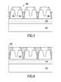
- FIG. 3illustrates a cross-sectional view of an array of recessed gate structures produced in block 202 of FIG. 2 , under an embodiment.
- the full arraymay be four, eight, or any number of devices, depending upon the specific device architecture.
- Embodiments of the process of FIG. 2can be applied to arrays of any appropriate number of devices.
- a buried oxide layer 304is present on a substrate layer 302 , and an SOI layer 306 is present on the buried oxide layer 304 .
- Each devicehas a recessed gate area 308 which may be formed by an etch process in which a mask pattern is placed over the SOI body layer 306 to allow partial removal of material to form the recess region 308 .
- Spacers 310are formed on either side of the gate 312 .
- the spacers 310are of a defined width depending on the desired circuit dimensions and constraints of the manufacturing system. In one embodiment, silicon nitride and silicon dioxide are used as the spacer and insulative materials respectively.
- any suitable materials that have high etch selectivelymay also be used, such as Tantalum Oxide (Ta 2 O 5 ), Titanium Oxide (TiO 2 ), Zirconium Oxide (ZrO 2 ), Hafnium Oxide (HfO 2 ), Aluminum Oxide (Al 2 O 3 ), and other such insulators or combinations of insulators.
- the spacer region and the top layer of the poly gateare made of the same material, and the gap region is filled with a different insulative or dielectric material.
- the spacer region and the top layer of the poly gatemay be of different materials, as long as selectivity to the interlayer dielectric (ILD) and silicon layers is achieved.
- a self-aligned lateral isolation trenchis formed to provide isolation between the devices of the array. As shown in FIG. 2 , this step involves etching through the dielectric layer 307 and the SOI layer 306 all the way down to the buried oxide layer 304 , block 204 . In an embodiment, this step can be combined with the self aligned contact etch process.
- the gate 312is separated from the underlying silicon body 306 by a thin gate oxide (not shown) that is also an insulator or insulative layer. This and other layers that may be grown during processing of the device are not shown to simplify the figures and to prevent unduly complicating the description.
- FIG. 4illustrates a cross-sectional view of an array of recessed gate structures produced in block 204 of FIG. 2 , under an embodiment.
- the etch step of block 204creates a lateral isolation trench 402 between each pair of devices.
- the lateral isolation trench 402defines a self-aligned contact area for each adjacent device.
- the width of lateral isolation trench 402is defined by the width of adjacent pairs of spacers 310 disposed on either side of each device gate 312 .
- the lateral isolation trench 402is self-aligned to the gate and spacers of neighboring devices.
- the lateral isolation trench 402is created through an etch process that does not require any lithography processes.
- the spacers 310are made of Silicon Nitride, and the etch can be made to be selective to Silicon, but not Silicon Nitride. Because lithography is not used to produce the contact area 402 , the contact area is not constrained by design rules or the need for overlay tolerances. Because the isolation trench is self aligned to the device gate/spacer, there is no need to provide a tolerance to ensure that the gate is precisely between a pair of isolation regions. This eliminates the need to increase the space between devices by the overlay tolerance. For example, if the gate width is on the order of 54 nm, the contact area 402 can be on the order of 20 nm or less.
- the lateral isolation trench for the contact areais partially filled with a dielectric material, such as Silicon Oxide.
- the partial fillis performed by filling the trench 402 back to the top or near the top of the dielectric layer 307 and then etching back down through the dielectric layer and through a portion of the SOI layer.
- the isolation trench 402is illustrated as a tapered trench that is narrower at the bottom than at the top. This shape reduces the possibility of creating a fill seam.
- the sides of the trenchmay be vertical or substantially vertical. In this case, as long as the sides are completely isolated with dielectric, it does not matter whether or not there is a fill seam.
- Other profilesmay be possible as well, such as a trench that expands at the bottom or has a rounded cross-sectional aspect to create a more optimum electrical field.
- the trenchcan be formed to have rounded aspect so that the bottom is curved.
- the actual shape of the trenchcan be controlled by standard trench formation techniques, such as altering the passivation amount to control the rate and direction of the etch process.
- FIG. 5illustrates a cross-sectional view of an array of recessed gate structures produced in block 206 of FIG. 2 , under an embodiment.
- isolation trench 402is partially filled with a dielectric material 502 .
- the dielectric materialshould be filled to an amount so that it is below the top of the silicon layer 306 and above the bottom of the recessed gate 308 .
- the exact height of the dielectric material 502 within trench 402may be determined by a number of factors, such as the out-diffusion methodology to create the source and drain regions of the device, as well as the gate size and gate recess depth. Other factors may also be considered in determining this process feature, depending upon the constraints and requirements of the device.
- the remaining hole area created by the partial etch of the dielectric material within the isolation trenchis then filled with highly doped polysilicon.
- the procedurecan be performed in several different ways, such as predoping the area with angled implants, and other similar techniques.
- FIG. 6illustrates the filling of the isolation trench above the silicon dioxide layer with a portion of doped polysilicon, under an embodiment.
- a layer of doped polysilicon 602is deposited above the silicon oxide layer 502 in isolation trench 402 .
- the doped polysilicon layerfills the isolation trenches to the top of the dielectric material 502 level in each isolation trench 402 .
- the doped polysilicon fill material 602is then planarized to be made flush with the dielectric layer 307 .
- a thermal cyclethen applied to out-diffuse the doped conductor material to form the source and drain regions of the device.
- the fill materialcan be accomplished by any appropriate planarization technique, such as CMP (Chemical Mechanical Planarization).
- FIG. 7illustrates devices with source and drain regions produced by out-diffusion of the doped polysilicon layer, under an embodiment.
- the planarized doped conductor 702out-diffuses when subject to a thermal cycle to form doped source and drain regions 704 .
- one or more thermal cyclescan be applied to the doped polysilicon to create source and drain regions proximate the floating body region.
- the embodiment of FIG. 7shows a standard configuration of the source and drain region 704 in a recessed gate device. That is, the source and drain regions 704 extend from the isolation trench 402 to the recessed gate 308 .
- the source and drain regions that are created by the out-diffusion process of the doped polysiliconcan be in formed in various different orientations and sizes with respect to the isolation trench and the recessed gate.
- the thermal cycleis shortened so that the doped polysilicon 702 only partially diffuses.
- the source and drain regiondo not extend to the gate oxide region. This is illustrated as block 212 of FIG. 2 .
- Alternate techniques to the doped polysilicon diffusion processmay be used to create the source and drain areas. For example, other solid source diffusion techniques or various implantation techniques may be used.
- FIG. 8illustrates the formation of source and drain regions in a recessed gate device, under an alternative embodiment. As shown in FIG. 8 , the source and drain regions 802 extend from the Silicon Oxide filled trench 402 , but do not extend to the gate oxide region of recessed gate 308 .
- FIG. 8illustrates an underlapped device which can reduce the GIDL effect by removing the source and drain regions from the immediate proximity of the gate.
- the amount of underlap determined by the distance of the source/drain region from the gate oxide areacan be altered depending on various factors such as gate size, tolerance to drain leakage, device turn-on and turn-off requirements, and the like.
- the electric field from the gateinteracts minimally with the source-drain junction. This arrangement is an inherent feature of the manufacturing process according to embodiments. By altering one or more processing parameters, any degree of underlap may be produced.
- the spacer 310comprises silicon nitride (Si 3 N 4 ), as does the insulative layer of the poly gate.
- the area between the spacerscontacts the source/drain areas, and is filled with a dielectric material, such as silicon dioxide (SiO 2 ).
- a dielectric materialsuch as silicon dioxide (SiO 2 ).
- the silicon dioxide layeris deposited and then polished to allow for straight line lithography on a planar surface.
- the elongated line defined by the spacersis etched using a selective etch process that removes the insulative material down to the silicon layer.
- the silicon nitridecomprising the spacer region and the film on top of the conductive gate, act as an etch stop.
- Embodiments of the device array manufacturing processcan be applied to any type of transistor based integrated circuit device or array that is manufactured in layers using photolithographic techniques.
- embodimentscan be used to produce any type of device in which a long transistor is required in a small area.
- Embodimentscan also be used to produce standalone memory devices.
- methods according to embodimentscan be used to produce standalone memory devices based on single transistor bit cells, and such devices can encompass Z-RAM® cells, or any similar memory cell that does not require a trench capacitor or similar component.
- aspects of the embodiments described hereinmay include a method of fabricating semiconductor memory cells comprising: forming a plurality of recessed gate devices on a silicon-on-insulator substrate formed over a buried oxide layer, each recessed gate device comprising a floating body region and spacers disposed on opposite sides of the floating body region; etching the silicon-on-insulator substrate until the buried oxide layer is reached to form a lateral isolation trench aligned to the gate by the spacer width; partially filling the lateral isolation trench with a dielectric material; filling a remaining portion of the lateral isolation trench with doped polysilicon; and thermally cycling the doped polysilicon to create source and drain regions proximate the floating body region.
- the source and drain regionsextend from the lateral isolation trench to the gate region.
- the source and drain regionsextend from the lateral isolation trench and do not contact the gate region.
- contact areas of a deviceare formed by a computer-controlled fabrication process executing instructions operable to: define an insulative spacer region on opposing sides of a silicon-on-insulator transistor gate, create a lateral isolation trench between two adjacent transistor gates that is self-aligned to the gates and that is formed through a non-lithographic process so as to be unconstrained by lithography design rules to form an array of SOI devices that are isolated by sub-feature size isolation regions.
- a semiconductor manufacturing processmay be implemented in a computer or machine implemented system executed on a digital processing system that controls one or more manufacturing machines. Aspects of the manufacturing process and process flow described herein may be executed by a computer executing program instructions, or as functionality programmed into any of a variety of circuitry for semiconductor processing programs or equipment. Such programs and equipment can be embodied in various different circuits, components, or systems, including programmable logic devices (“PLDs”), such as field programmable gate arrays (“FPGAs”), programmable array logic (“PAL”) devices, electrically programmable logic and memory devices and standard cell-based devices, as well as application specific integrated circuits.
- PLDsprogrammable logic devices
- FPGAsfield programmable gate arrays
- PALprogrammable array logic
- microcontrollers with memorysuch as EEPROM
- embedded microprocessorsfirmware, software, etc.
- aspects of the described methodmay be embodied in microprocessors having software-based circuit emulation, discrete logic (sequential and combinatorial), custom devices, fuzzy (neural) logic, quantum devices, and hybrids of any of the above device types.
- Computer-readable media in which such formatted data and/or instructions may be embodiedinclude, but are not limited to, storage media in various forms (e.g., optical, magnetic or semiconductor storage media) and carrier waves that may be used to transfer such formatted data and/or instructions through wireless, optical, or wired signaling media or any combination thereof.
- Examples of transfers of such formatted data and/or instructions by carrier wavesinclude, but are not limited to, transfers (uploads, downloads, e-mail, etc.) over the Internet and/or other computer networks via one or more data transfer protocols (e.g., HTTP, FTP, SMTP, and so on).
- transfersuploads, downloads, e-mail, etc.
- data transfer protocolse.g., HTTP, FTP, SMTP, and so on.
- the words “comprise,” “comprising,” and the likeare to be construed in an inclusive sense as opposed to an exclusive or exhaustive sense; that is to say, in a sense of “including, but not limited to.” Words using the singular or plural number also include the plural or singular number respectively. Additionally, the words “herein,” “hereunder,” “above,” “below,” and words of similar import refer to this application as a whole and not to any particular portions of this application. When the word “or” is used in reference to a list of two or more items, that word covers all of the following interpretations of the word: any of the items in the list, all of the items in the list and any combination of the items in the list.
- Such computer readable mediamay store instructions that are to be executed by a computing device (e.g., personal computer, personal digital assistant, PVR, mobile device or the like) or may be instructions (such as, for example, Verilog or a hardware description language) that when executed are designed to create a device (GPU, ASIC, or the like) or software application that when operated performs aspects described above.
- a computing devicee.g., personal computer, personal digital assistant, PVR, mobile device or the like
- instructionssuch as, for example, Verilog or a hardware description language
- the claimed inventionmay be embodied in computer code (e.g., HDL, Verilog, etc.) that is created, stored, synthesized, and used to generate GDSII data (or its equivalent). One or more semiconductor devices, arrays, circuits or any combination thereof may then be manufactured based on this data.
- computer codee.g., HDL, Verilog, etc.
- One or more semiconductor devices, arrays, circuits or any combination thereofmay then be manufactured based on this data.
Landscapes
- Semiconductor Memories (AREA)
- Insulated Gate Type Field-Effect Transistor (AREA)
- Thin Film Transistor (AREA)
- Element Separation (AREA)
Abstract
Description
- The present application claims the benefit of the U.S. Provisional Application No. 61/100,040 entitled “Recessed Gate Silicon-on-Insulator Floating Body Device with Self-Aligned Lateral Isolation,” and filed on Sep. 25, 2008, which is hereby incorporated by reference in its entirety.
- Embodiments of the invention relate generally to semiconductor manufacturing, and more specifically to manufacturing processes for memory cell circuits.
- Computing systems typically move vast amounts of data and have three types or levels of memory: on-chip or embedded memory in the processor itself (e.g., embedded SRAM or embedded DRAM), main memory (e.g., standalone DRAM), and non-volatile memory (e.g., hard disk drives, magnetic tape, etc.). Dynamic Random Access Memory (DRAM) is essentially used as the main memory of the system. Over the years, the electronics industry has developed DRAM memories that feature reduced bit cell sizes, higher densities, and reduced costs. In order to gain further cost and miniaturization advantages, a great deal of emphasis has been placed on reducing bit cell size to maximize the amount of memory available in a given amount of silicon area. One important parameter associated with semiconductor memories, such as DRAM devices is the feature size of the transistor device that comprises the memory cell. In general, the feature size of the transistor is denoted F, where F corresponds to the minimum gate length that can be produced in the manufacturing process for a circuit. Under present manufacturing systems, the bit-cell area for a one-transistor, one-capacitor DRAM device is typically on the order of 2 F by 3 F to 4 F, which corresponds to a total area of 6 F2to 8F2.
- DRAM devices have traditionally been made using a simple one-transistor/one-capacitor structure for the basis of each storage cell. Transistor scaling for ever-smaller (higher density) devices presents many challenges. Among others, at small dimensions, various parasitic effects start to appear. Various processing technologies have been developed to overcome these effects, and allow the continuing miniaturization of microelectronic devices. One such technology is Silicon-on-Insulator (SOI) technology, in which a layered silicon-insulator substrate is used in place of conventional silicon substrates. In an SOI device, the active circuit layer is isolated from the substrate. SOI transistors generally have an electrically floating body region. Recent technology has been developed to use this floating-body as an alternative to discrete-trench or stacked-capacitor structures to store information and create a memory bit cell. One such technology is represented by Z-RAM® cells, which consist of a single transistor per bit-cell, with zero capacitors, thus eliminating the deep trench or the complex stacked capacitor. Z-RAM® was developed by, and is a trademark of Innovative Silicon, Inc. of Switzerland. Aspects of the Z-RAM technology, devices, and manufacture are described in the following United States Patent Applications, among others: U.S. application Ser. No. 12/053,398, filed Mar. 21, 2008, and entitled “Manufacturing Process for Zero-Capacitor Random Access Memory Circuits,” and U.S. application Ser. No. 12/019,320, filed Jan. 24, 2008, and entitled “Semiconductor Device with Electrically Floating Body,” each of which is herein incorporated by reference in its entirety.
- For SOI structures, the floating body effect is usually an undesirable parasitic element. Embodiments of the present invention are directed to using the parasitic floating body effect advantageously as the basis for various new processing technologies. Such embodiments can be applied to SOI processing technology, as well as any other similar isolated body process technology.
- As the channel lengths of DRAM devices become smaller, the densities of the devices increase. In the case of a planar transistor, the channel length of the transistor is reduced as the integration density increases. This, in turn, increases the so-called short-channel effect. In a MOSFET device, a short-channel configuration occurs when the channel length is the same order of magnitude as the depletion-layer widths of the source and drain junctions. Short-channel effects can be attributed to the limitation imposed on electron drift characteristics in the channel, and a modification of the device threshold voltage due to shortened channel length. As channel lengths are excessively decreased in planar devices, the likelihood of a device “punchthrough” effect between the source and a drain of the device is increased, resulting in malfunction of the device. Punchthrough can occur when a high voltage is placed across the transistor from the source to the drain. In this case, an undesirable conductive path is formed through the body region when the transistor should be off One solution to the punchthrough problem is the use of recessed gate manufacturing techniques in which the transistor is made with a three-dimensional shape having a recessed channel to create a recessed channel (or recessed gate) transistor. The recessed gate effectively creates a long gate length of a device without increasing the feature size of the cell due to the vertical orientation of the device in which the current flows in three-dimensions.
- In general, the standard method of creating a recessed gate device is not used in an SOI device.
FIG. 1 illustrates a partial array of three separate DRAM cells manufactured from SOI technology, under an embodiment. As shown inFIG. 1 , abarrier layer 104 is formed on asemiconductor substrate 102. Thebarrier layer 104 may be formed of an oxide layer, such as the buried oxide layer (BOX) in an SOI substrate, although it may also be created by other means. Abody layer 106 is formed on thebarrier layer 104, and may be formed of single crystalline silicon by an epitaxy method or by the SOI substrate fabrication process. In the SOI device shown inFIG. 1 , each device is fully isolated from every other device in the array. As shown inFIG. 1 , thedevices isolation layers 108. Theisolation layers 108 are formed withinbody layer 106 and may be formed of an insulating layer, such as a high density plasma oxide layer and/or a silicon oxide layer by chemical vapor deposition, or similar methods. As shown inFIG. 1A , theisolation layers 108 extend to the surface or near the surface of thebarrier layer 104. Isolation regions can be provided in two dimensions, however such isolation regions are typically created using lithography methods. That is, they are pre-etched before the gate is formed as done in a standard STI (shallow trench isolation) process. Consequently, the isolation regions are strictly bound by lithography dimension requirements. - In
FIG. 1 , thegate 110 is separated from theunderlying silicon body 106 by a thin gate oxide (not shown) that is also an insulator or insulative layer. This and other layers that may be grown during processing of the device are not shown, but should be understood to be present by those of ordinary skill in the art. - The basic dimension of each cell is defined by the length of the
gate 110 of each device. As stated above, this represents the feature size of the transistor (F). For present manufacturing processes, such as illustrated inFIG. 1 , the need for substantial isolation between each cell requires that the dimensions of a cell array be a multiple of the individual feature size, F. This is due to the fact that present lithography-based technologies require a minimum printable feature size. This further adds to increased spacing between cells in an array, as well as extra photolithography processing steps. - What is desired, therefore, is a device manufacturing process that creates cell arrays of a minimal dimension and that is not limited by present lithography node rules.
- What is further desired is a process that creates a self-aligned lateral isolation for an SOI recessed gate device.
- What is yet further desired is a device manufacturing process that efficiently creates an underlap device to reduce the gate induced drain leakage (GIDL) effect.
- Each patent, patent application, and/or publication mentioned in this specification is herein incorporated by reference in its entirety to the same extent as if each individual patent, patent application, and/or publication was specifically and individually indicated to be incorporated by reference.
- In the course of the detailed description to follow, reference will be made to the attached drawings. These drawings show different aspects of embodiments of the present invention and, where appropriate, reference numerals illustrating like structures, components, materials and/or elements in different figures are labeled similarly. It is understood that various combinations of the structures, components, materials and/or elements, other than those specifically shown, are contemplated and are within the scope of the described embodiments. Moreover, there are many inventions described and illustrated herein. The present inventions are neither limited to any single aspect nor embodiment thereof, nor to any combinations and/or permutations of such aspects and/or embodiments. Moreover, each of the aspects of the present inventions, and/or embodiments thereof, may be employed in combination with one or more other aspects of the present inventions, and/or embodiments thereof. For the sake of brevity, many of those permutations and combinations are not discussed separately herein.
- Embodiments of the present invention are illustrated by way of example and not limitation in the figures of the accompanying drawings, in which like references indicate similar elements and in which:
FIG. 1 illustrates a partial array of floating-body, Silicon-on-Insulator integrated circuit devices, produced by prior art processes.FIG. 2 is a flowchart illustrating a process of producing a recessed gate device, Silicon-on-Insulator device with self-aligned lateral isolation, under an embodiment.FIG. 3 illustrates an initial process step of producing a recessed gate device, Silicon-on-Insulator device with self-aligned lateral isolation, under an embodiment.FIG. 4 illustrates a subsequent process step of producing a recessed gate device, Silicon-on-Insulator device with self-aligned lateral isolation, under an embodiment.FIG. 5 illustrates a further subsequent process step of producing a recessed gate device, Silicon-on-Insulator device with self-aligned lateral isolation, under an embodiment.FIG. 6 illustrates a yet further subsequent process step of producing a recessed gate device, Silicon-on-Insulator device with self-aligned lateral isolation, under an embodiment.FIG. 7 illustrates devices with source and drain regions produced by out-diffusion of the doped polysilicon layer, under an embodiment.FIG. 8 illustrates the formation of source and drain regions in a recessed gate device, under an alternative embodiment.- Embodiments of a manufacturing process for producing recessed-gate, Silicon-on-Insulator integrated circuit devices with self-aligned, lateral isolation, are described. The process according to these embodiments allows for the creation of true in-pitch recessed gate devices without requiring an extra isolation dimension. A lateral isolation trench is formed between pairs of recessed gate devices by etching the silicon-on-insulator area down to a buried oxide layer on which the silicon-on-insulator layer is formed. The position of the trench is self-aligned and defined by the gate length and the dimension of spacers disposed on either side of the gate. The trench is formed by a non-lithographic etch process. The isolation trench is filled with a dielectric material and then etched back to somewhere in the middle of the SOI body, the location being as required by the optimization of the device characteristics. The remaining volume of the trench is filled with a doped conductive material such as an in-situ, n-doped poly material, although any dopant type or species can be used as necessary to create the correct device characteristics. The doped conductor is subject to a thermal cycle to create source and drain regions of the device through out-diffusion of the doped material. The source and drain regions may be formed at a defined distance from the gate to produce an underlapped device that is advantageously immune to gate induced drain leakage effects.
- In the following description, numerous specific details are introduced to provide a thorough understanding of, and enabling description for, embodiments of an integrated circuit manufacturing process. One skilled in the relevant art, however, will recognize that these embodiments can be practiced without one or more of the specific details, or with other components, systems, and so on. In other instances, well-known structures or operations are not shown, or are not described in detail, to avoid obscuring aspects of the disclosed embodiments.
- Silicon-on-Insulator (SOI) processes refer to the use of a layered silicon-insulator-silicon substrate instead of conventional silicon substrates in semiconductor manufacturing. Unlike conventional CMOS chips, where a transistor is placed directly on the surface of a silicon substrate, an SOI device has a thick layer of insulator (typically silicon dioxide) between the transistor and the silicon substrate to efficiently isolate transistors from the substrate. Note that after creation of a lateral isolation, the transistors become fully isolated from adjacent devices. On standard SOI wafers, there is a buried oxide layer that covers the complete surface of the wafer, and this use of a layered silicon-insulator-silicon substrate in place of a conventional silicon substrate generally reduces parasitic device capacitance or leakages and thereby improves device performances. SOI-based devices also differ from conventional silicon-built devices in that the silicon junction is above an electrical insulator, which typically is silicon dioxide.
- Embodiments are directed to a manufacturing process that creates a recessed gate structure on an SOI substrate that features self-aligned lateral isolation. The lateral isolation dimension is sub-feature size so that an array of devices can be made substantially smaller than is allowed by present lithography techniques. The isolation regions between each device in the array are self-aligned to the gate and spacer of an adjacent device and are formed during post-gate production using a non-patterned process so that no etch tolerance is required for overlap error. This allows the creation of a fully isolated device that is of dimension 4F2as opposed to 6 to 8F2, which is the typical size for devices in present DRAM arrays with full isolation. Such a method is particularly useful in, but not limited to, applications related to the manufacture of new generation memory devices.
FIG. 2 is a flowchart illustrating an overall process of producing a recessed gate SOI with self-aligned lateral isolation, under an embodiment. The process first creates a recessed gate device on an SOI substrate,process block 202. This step may utilize standard known methods of creating a recessed gate device. During this step, spacers are formed and an interlayer dielectric (ILD) layer is filled and planarized. This is followed by acontact etch process 204 in which the SOI layer is etched until the buried oxide layer is reached so that a self-aligned lateral isolation trench is formed. Inprocess block 206, the lateral isolation trench is filled with a dielectric material, and then etched back to the SOI layer. Source-drain regions are then created through content poly fill, planarization, and out-diffusion processes, block210. The source-drain regions are then separated from the surface channel of the gate to reduce to reduce possible gate induced drain leakage (GIDL) effects, block212. Details of each of the process blocks ofFIG. 2 are provided in the description that follows.FIG. 3 illustrates a cross-sectional view of an array of recessed gate structures produced inblock 202 ofFIG. 2 , under an embodiment. Apartial array 300 of three identical devices, shown across a single row, is illustrated. The full array may be four, eight, or any number of devices, depending upon the specific device architecture. Embodiments of the process ofFIG. 2 can be applied to arrays of any appropriate number of devices.- As shown in
FIG. 3 , a buriedoxide layer 304 is present on asubstrate layer 302, and anSOI layer 306 is present on the buriedoxide layer 304. Each device has a recessedgate area 308 which may be formed by an etch process in which a mask pattern is placed over theSOI body layer 306 to allow partial removal of material to form therecess region 308.Spacers 310 are formed on either side of thegate 312. Thespacers 310 are of a defined width depending on the desired circuit dimensions and constraints of the manufacturing system. In one embodiment, silicon nitride and silicon dioxide are used as the spacer and insulative materials respectively. Alternatively, any suitable materials that have high etch selectively may also be used, such as Tantalum Oxide (Ta2O5), Titanium Oxide (TiO2), Zirconium Oxide (ZrO2), Hafnium Oxide (HfO2), Aluminum Oxide (Al2O3), and other such insulators or combinations of insulators. In general, the spacer region and the top layer of the poly gate are made of the same material, and the gap region is filled with a different insulative or dielectric material. In certain cases, the spacer region and the top layer of the poly gate may be of different materials, as long as selectivity to the interlayer dielectric (ILD) and silicon layers is achieved. Once the recessed gate structures are formed inblock 202, a self-aligned lateral isolation trench is formed to provide isolation between the devices of the array. As shown inFIG. 2 , this step involves etching through thedielectric layer 307 and theSOI layer 306 all the way down to the buriedoxide layer 304, block204. In an embodiment, this step can be combined with the self aligned contact etch process. - In
FIG. 3 and the following related figures, thegate 312 is separated from theunderlying silicon body 306 by a thin gate oxide (not shown) that is also an insulator or insulative layer. This and other layers that may be grown during processing of the device are not shown to simplify the figures and to prevent unduly complicating the description. FIG. 4 illustrates a cross-sectional view of an array of recessed gate structures produced inblock 204 ofFIG. 2 , under an embodiment. The etch step ofblock 204 creates alateral isolation trench 402 between each pair of devices. Thelateral isolation trench 402 defines a self-aligned contact area for each adjacent device. The width oflateral isolation trench 402 is defined by the width of adjacent pairs ofspacers 310 disposed on either side of eachdevice gate 312. Thelateral isolation trench 402 is self-aligned to the gate and spacers of neighboring devices. In a preferred embodiment, thelateral isolation trench 402 is created through an etch process that does not require any lithography processes. For this embodiment, thespacers 310 are made of Silicon Nitride, and the etch can be made to be selective to Silicon, but not Silicon Nitride. Because lithography is not used to produce thecontact area 402, the contact area is not constrained by design rules or the need for overlay tolerances. Because the isolation trench is self aligned to the device gate/spacer, there is no need to provide a tolerance to ensure that the gate is precisely between a pair of isolation regions. This eliminates the need to increase the space between devices by the overlay tolerance. For example, if the gate width is on the order of 54 nm, thecontact area 402 can be on the order of 20 nm or less.- With reference to
FIG. 2 , as shown inblock 206, once the lateral isolation trench for the contact area is formed, it is partially filled with a dielectric material, such as Silicon Oxide. In one embodiment, the partial fill is performed by filling thetrench 402 back to the top or near the top of thedielectric layer 307 and then etching back down through the dielectric layer and through a portion of the SOI layer. - For the embodiment of
FIG. 4 , theisolation trench 402 is illustrated as a tapered trench that is narrower at the bottom than at the top. This shape reduces the possibility of creating a fill seam. Alternatively, the sides of the trench may be vertical or substantially vertical. In this case, as long as the sides are completely isolated with dielectric, it does not matter whether or not there is a fill seam. Other profiles may be possible as well, such as a trench that expands at the bottom or has a rounded cross-sectional aspect to create a more optimum electrical field. Alternatively, the trench can be formed to have rounded aspect so that the bottom is curved. The actual shape of the trench can be controlled by standard trench formation techniques, such as altering the passivation amount to control the rate and direction of the etch process. FIG. 5 illustrates a cross-sectional view of an array of recessed gate structures produced inblock 206 ofFIG. 2 , under an embodiment. As shown inFIG. 5 ,isolation trench 402 is partially filled with adielectric material 502. The dielectric material should be filled to an amount so that it is below the top of thesilicon layer 306 and above the bottom of the recessedgate 308. The exact height of thedielectric material 502 withintrench 402 may be determined by a number of factors, such as the out-diffusion methodology to create the source and drain regions of the device, as well as the gate size and gate recess depth. Other factors may also be considered in determining this process feature, depending upon the constraints and requirements of the device.- The remaining hole area created by the partial etch of the dielectric material within the isolation trench is then filled with highly doped polysilicon. The procedure can be performed in several different ways, such as predoping the area with angled implants, and other similar techniques.
FIG. 6 illustrates the filling of the isolation trench above the silicon dioxide layer with a portion of doped polysilicon, under an embodiment. As can be seen inFIG. 6 , a layer of dopedpolysilicon 602 is deposited above thesilicon oxide layer 502 inisolation trench 402. The doped polysilicon layer fills the isolation trenches to the top of thedielectric material 502 level in eachisolation trench 402. As shown inblock 210 ofFIG. 2 , the dopedpolysilicon fill material 602 is then planarized to be made flush with thedielectric layer 307. A thermal cycle then applied to out-diffuse the doped conductor material to form the source and drain regions of the device. The fill material can be accomplished by any appropriate planarization technique, such as CMP (Chemical Mechanical Planarization).FIG. 7 illustrates devices with source and drain regions produced by out-diffusion of the doped polysilicon layer, under an embodiment. The planarizeddoped conductor 702 out-diffuses when subject to a thermal cycle to form doped source and drainregions 704. Depending upon process requirements and constraints, one or more thermal cycles can be applied to the doped polysilicon to create source and drain regions proximate the floating body region. The embodiment ofFIG. 7 shows a standard configuration of the source and drainregion 704 in a recessed gate device. That is, the source and drainregions 704 extend from theisolation trench 402 to the recessedgate 308.- In an alternative embodiment, the source and drain regions that are created by the out-diffusion process of the doped polysilicon can be in formed in various different orientations and sizes with respect to the isolation trench and the recessed gate. In one embodiment, the thermal cycle is shortened so that the doped
polysilicon 702 only partially diffuses. For this embodiment, the source and drain region do not extend to the gate oxide region. This is illustrated asblock 212 ofFIG. 2 . - Alternate techniques to the doped polysilicon diffusion process may be used to create the source and drain areas. For example, other solid source diffusion techniques or various implantation techniques may be used.
FIG. 8 illustrates the formation of source and drain regions in a recessed gate device, under an alternative embodiment. As shown inFIG. 8 , the source and drainregions 802 extend from the Silicon Oxide filledtrench 402, but do not extend to the gate oxide region of recessedgate 308.- In general, the electric field is a device is at its highest concentration just beneath the gate of the device. This electric field can create a problem known as Gate Induced Drain Leakage (GIDL).
FIG. 8 illustrates an underlapped device which can reduce the GIDL effect by removing the source and drain regions from the immediate proximity of the gate. The amount of underlap determined by the distance of the source/drain region from the gate oxide area can be altered depending on various factors such as gate size, tolerance to drain leakage, device turn-on and turn-off requirements, and the like. In the underlap device ofFIG. 8 , the electric field from the gate interacts minimally with the source-drain junction. This arrangement is an inherent feature of the manufacturing process according to embodiments. By altering one or more processing parameters, any degree of underlap may be produced. - Although embodiments have been described with respect to specific materials and processing methods, it should be understood that various alternatives are possible. For example, in one embodiment of the memory array produced by a method according to embodiments, the
spacer 310 comprises silicon nitride (Si3N4), as does the insulative layer of the poly gate. The area between the spacers contacts the source/drain areas, and is filled with a dielectric material, such as silicon dioxide (SiO2). After the nitride spacers have been formed, the silicon dioxide layer is deposited and then polished to allow for straight line lithography on a planar surface. The elongated line defined by the spacers is etched using a selective etch process that removes the insulative material down to the silicon layer. The silicon nitride comprising the spacer region and the film on top of the conductive gate, act as an etch stop. - Embodiments of the device array manufacturing process can be applied to any type of transistor based integrated circuit device or array that is manufactured in layers using photolithographic techniques. In general, embodiments can be used to produce any type of device in which a long transistor is required in a small area. Embodiments can also be used to produce standalone memory devices. In general, methods according to embodiments can be used to produce standalone memory devices based on single transistor bit cells, and such devices can encompass Z-RAM® cells, or any similar memory cell that does not require a trench capacitor or similar component.
- Aspects of the embodiments described herein may include a method of fabricating semiconductor memory cells comprising: forming a plurality of recessed gate devices on a silicon-on-insulator substrate formed over a buried oxide layer, each recessed gate device comprising a floating body region and spacers disposed on opposite sides of the floating body region; etching the silicon-on-insulator substrate until the buried oxide layer is reached to form a lateral isolation trench aligned to the gate by the spacer width; partially filling the lateral isolation trench with a dielectric material; filling a remaining portion of the lateral isolation trench with doped polysilicon; and thermally cycling the doped polysilicon to create source and drain regions proximate the floating body region. In an embodiment, the source and drain regions extend from the lateral isolation trench to the gate region. In an alternative embodiment, the source and drain regions extend from the lateral isolation trench and do not contact the gate region.
- In an embodiment, contact areas of a device are formed by a computer-controlled fabrication process executing instructions operable to: define an insulative spacer region on opposing sides of a silicon-on-insulator transistor gate, create a lateral isolation trench between two adjacent transistor gates that is self-aligned to the gates and that is formed through a non-lithographic process so as to be unconstrained by lithography design rules to form an array of SOI devices that are isolated by sub-feature size isolation regions.
- A semiconductor manufacturing process according to embodiments may be implemented in a computer or machine implemented system executed on a digital processing system that controls one or more manufacturing machines. Aspects of the manufacturing process and process flow described herein may be executed by a computer executing program instructions, or as functionality programmed into any of a variety of circuitry for semiconductor processing programs or equipment. Such programs and equipment can be embodied in various different circuits, components, or systems, including programmable logic devices (“PLDs”), such as field programmable gate arrays (“FPGAs”), programmable array logic (“PAL”) devices, electrically programmable logic and memory devices and standard cell-based devices, as well as application specific integrated circuits. Some other possibilities for implementing aspects of the semiconductor manufacturing system include: microcontrollers with memory (such as EEPROM), embedded microprocessors, firmware, software, etc. Furthermore, aspects of the described method may be embodied in microprocessors having software-based circuit emulation, discrete logic (sequential and combinatorial), custom devices, fuzzy (neural) logic, quantum devices, and hybrids of any of the above device types.
- It should also be noted that the various functions disclosed herein may be described using any number of combinations of hardware, firmware, and/or as data and/or instructions embodied in various machine-readable or computer-readable media, in terms of their behavioral, register transfer, logic component, and/or other characteristics. Computer-readable media in which such formatted data and/or instructions may be embodied include, but are not limited to, storage media in various forms (e.g., optical, magnetic or semiconductor storage media) and carrier waves that may be used to transfer such formatted data and/or instructions through wireless, optical, or wired signaling media or any combination thereof. Examples of transfers of such formatted data and/or instructions by carrier waves include, but are not limited to, transfers (uploads, downloads, e-mail, etc.) over the Internet and/or other computer networks via one or more data transfer protocols (e.g., HTTP, FTP, SMTP, and so on).
- Unless the context clearly requires otherwise, throughout the description and any present claims, the words “comprise,” “comprising,” and the like are to be construed in an inclusive sense as opposed to an exclusive or exhaustive sense; that is to say, in a sense of “including, but not limited to.” Words using the singular or plural number also include the plural or singular number respectively. Additionally, the words “herein,” “hereunder,” “above,” “below,” and words of similar import refer to this application as a whole and not to any particular portions of this application. When the word “or” is used in reference to a list of two or more items, that word covers all of the following interpretations of the word: any of the items in the list, all of the items in the list and any combination of the items in the list.
- The above description of illustrated embodiments of the semiconductor manufacturing process and system is not intended to be exhaustive or to limit the embodiments to the precise form or instructions disclosed. While specific embodiments of, and examples are described herein for illustrative purposes, various equivalent modifications are possible within the scope of the described embodiments, as those skilled in the relevant art will recognize.
- The elements and acts of the various embodiments described above can be combined to provide further embodiments. These and other changes can be made to the semiconductor manufacturing process in light of the above detailed description.
- In general, in the following, the terms used should not be construed to limit the described system to the specific embodiments disclosed in the specification, but should be construed to include all operations or processes that operate thereunder.
- While certain aspects of the disclosed method and system may be presented below in certain forms, the inventor contemplates the various aspects of the methodology in any number of forms. For example, while only one aspect of the describe process may be recited as embodied in machine-readable medium, other aspects may likewise be embodied in machine-readable medium. Such computer readable media may store instructions that are to be executed by a computing device (e.g., personal computer, personal digital assistant, PVR, mobile device or the like) or may be instructions (such as, for example, Verilog or a hardware description language) that when executed are designed to create a device (GPU, ASIC, or the like) or software application that when operated performs aspects described above. The claimed invention may be embodied in computer code (e.g., HDL, Verilog, etc.) that is created, stored, synthesized, and used to generate GDSII data (or its equivalent). One or more semiconductor devices, arrays, circuits or any combination thereof may then be manufactured based on this data.
Claims (20)
Priority Applications (3)
| Application Number | Priority Date | Filing Date | Title |
|---|---|---|---|
| US12/567,202US7947543B2 (en) | 2008-09-25 | 2009-09-25 | Recessed gate silicon-on-insulator floating body device with self-aligned lateral isolation |
| US13/113,839US8790968B2 (en) | 2008-09-25 | 2011-05-23 | Recessed gate silicon-on-insulator floating body device with self-aligned lateral isolation |
| US14/341,867US9553186B2 (en) | 2008-09-25 | 2014-07-28 | Recessed gate silicon-on-insulator floating body device with self-aligned lateral isolation |
Applications Claiming Priority (2)
| Application Number | Priority Date | Filing Date | Title |
|---|---|---|---|
| US10004008P | 2008-09-25 | 2008-09-25 | |
| US12/567,202US7947543B2 (en) | 2008-09-25 | 2009-09-25 | Recessed gate silicon-on-insulator floating body device with self-aligned lateral isolation |
Related Child Applications (1)
| Application Number | Title | Priority Date | Filing Date |
|---|---|---|---|
| US13/113,839DivisionUS8790968B2 (en) | 2008-09-25 | 2011-05-23 | Recessed gate silicon-on-insulator floating body device with self-aligned lateral isolation |
Publications (2)
| Publication Number | Publication Date |
|---|---|
| US20100075471A1true US20100075471A1 (en) | 2010-03-25 |
| US7947543B2 US7947543B2 (en) | 2011-05-24 |
Family
ID=42038087
Family Applications (3)
| Application Number | Title | Priority Date | Filing Date |
|---|---|---|---|
| US12/567,202ActiveUS7947543B2 (en) | 2008-09-25 | 2009-09-25 | Recessed gate silicon-on-insulator floating body device with self-aligned lateral isolation |
| US13/113,839Active2030-11-18US8790968B2 (en) | 2008-09-25 | 2011-05-23 | Recessed gate silicon-on-insulator floating body device with self-aligned lateral isolation |
| US14/341,867Expired - Fee RelatedUS9553186B2 (en) | 2008-09-25 | 2014-07-28 | Recessed gate silicon-on-insulator floating body device with self-aligned lateral isolation |
Family Applications After (2)
| Application Number | Title | Priority Date | Filing Date |
|---|---|---|---|
| US13/113,839Active2030-11-18US8790968B2 (en) | 2008-09-25 | 2011-05-23 | Recessed gate silicon-on-insulator floating body device with self-aligned lateral isolation |
| US14/341,867Expired - Fee RelatedUS9553186B2 (en) | 2008-09-25 | 2014-07-28 | Recessed gate silicon-on-insulator floating body device with self-aligned lateral isolation |
Country Status (1)
| Country | Link |
|---|---|
| US (3) | US7947543B2 (en) |
Cited By (2)
| Publication number | Priority date | Publication date | Assignee | Title |
|---|---|---|---|---|
| US20100197090A1 (en)* | 2009-02-03 | 2010-08-05 | Samsung Electronics Co., Ltd. | Method of fabricating semiconductor device having transistor |
| US20140054705A1 (en)* | 2012-08-27 | 2014-02-27 | International Business Machines Corporation | Silicon germanium channel with silicon buffer regions for fin field effect transistor device |
Families Citing this family (10)
| Publication number | Priority date | Publication date | Assignee | Title |
|---|---|---|---|---|
| US8093111B2 (en)* | 2008-07-29 | 2012-01-10 | Hynix Semiconductor Inc. | Semiconductor device including partial silicon on insulator fin structure and method for fabricating the same |
| US7947543B2 (en) | 2008-09-25 | 2011-05-24 | Micron Technology, Inc. | Recessed gate silicon-on-insulator floating body device with self-aligned lateral isolation |
| US9059292B2 (en) | 2012-08-02 | 2015-06-16 | International Business Machines Corporation | Source and drain doping profile control employing carbon-doped semiconductor material |
| US8841188B2 (en) | 2012-09-06 | 2014-09-23 | International Business Machines Corporation | Bulk finFET with controlled fin height and high-K liner |
| US9209094B2 (en) | 2013-07-29 | 2015-12-08 | Globalfoundries Inc. | Fin field effect transistor with dielectric isolation and anchored stressor elements |
| US9064943B1 (en) | 2014-09-30 | 2015-06-23 | International Business Machines Corporation | Gate-all-around field effect transistor structures and methods |
| US10818665B2 (en)* | 2018-08-24 | 2020-10-27 | Micron Technology, Inc. | Array of recessed access devices and an array of memory cells individually comprising a capacitor and a transistor |
| US10930734B2 (en) | 2018-10-30 | 2021-02-23 | International Business Machines Corporation | Nanosheet FET bottom isolation |
| US11011528B2 (en) | 2019-05-08 | 2021-05-18 | International Business Machines Corporation | Asymmetric gate edge spacing for SRAM structures |
| US12230673B2 (en) | 2022-03-30 | 2025-02-18 | Globalfoundries U.S. Inc. | Field-effect transistors having a gate electrode positioned inside a substrate recess |
Citations (95)
| Publication number | Priority date | Publication date | Assignee | Title |
|---|---|---|---|---|
| US3439214A (en)* | 1968-03-04 | 1969-04-15 | Fairchild Camera Instr Co | Beam-junction scan converter |
| US4250569A (en)* | 1978-11-15 | 1981-02-10 | Fujitsu Limited | Semiconductor memory device |
| US4262340A (en)* | 1978-11-14 | 1981-04-14 | Fujitsu Limited | Semiconductor memory device |
| US4371955A (en)* | 1979-02-22 | 1983-02-01 | Fujitsu Limited | Charge-pumping MOS FET memory device |
| US4658377A (en)* | 1984-07-26 | 1987-04-14 | Texas Instruments Incorporated | Dynamic memory array with segmented bit lines |
| US4807195A (en)* | 1987-05-18 | 1989-02-21 | International Business Machines Corporation | Apparatus and method for providing a dual sense amplifier with divided bit line isolation |
| US5010524A (en)* | 1989-04-20 | 1991-04-23 | International Business Machines Corporation | Crosstalk-shielded-bit-line dram |
| US5313432A (en)* | 1990-05-23 | 1994-05-17 | Texas Instruments Incorporated | Segmented, multiple-decoder memory array and method for programming a memory array |
| US5315541A (en)* | 1992-07-24 | 1994-05-24 | Sundisk Corporation | Segmented column memory array |
| US5388068A (en)* | 1990-05-02 | 1995-02-07 | Microelectronics & Computer Technology Corp. | Superconductor-semiconductor hybrid memory circuits with superconducting three-terminal switching devices |
| US5397726A (en)* | 1992-02-04 | 1995-03-14 | National Semiconductor Corporation | Segment-erasable flash EPROM |
| US5489792A (en)* | 1994-04-07 | 1996-02-06 | Regents Of The University Of California | Silicon-on-insulator transistors having improved current characteristics and reduced electrostatic discharge susceptibility |
| US5506436A (en)* | 1992-12-10 | 1996-04-09 | Sony Corporation | Semiconductor memory cell |
| US5515383A (en)* | 1991-05-28 | 1996-05-07 | The Boeing Company | Built-in self-test system and method for self test of an integrated circuit |
| US5593912A (en)* | 1994-10-06 | 1997-01-14 | International Business Machines Corporation | SOI trench DRAM cell for 256 MB DRAM and beyond |
| US5606188A (en)* | 1995-04-26 | 1997-02-25 | International Business Machines Corporation | Fabrication process and structure for a contacted-body silicon-on-insulator dynamic random access memory |
| US5608250A (en)* | 1993-11-29 | 1997-03-04 | Sgs-Thomson Microelectronics S.A. | Volatile memory cell with interface charge traps |
| US5627092A (en)* | 1994-09-26 | 1997-05-06 | Siemens Aktiengesellschaft | Deep trench dram process on SOI for low leakage DRAM cell |
| US5740099A (en)* | 1995-02-07 | 1998-04-14 | Nec Corporation | Semiconductor memory device having peripheral circuit and interface circuit fabricated on bulk region out of silicon-on-insulator region for memory cells |
| US5877978A (en)* | 1996-03-04 | 1999-03-02 | Mitsubishi Denki Kabushiki Kaisha | Semiconductor memory device |
| US5886385A (en)* | 1996-08-22 | 1999-03-23 | Kabushiki Kaisha Toshiba | Semiconductor device and manufacturing method thereof |
| US5886376A (en)* | 1996-07-01 | 1999-03-23 | International Business Machines Corporation | EEPROM having coplanar on-insulator FET and control gate |
| US5897351A (en)* | 1997-02-20 | 1999-04-27 | Micron Technology, Inc. | Method for forming merged transistor structure for gain memory cell |
| US6018172A (en)* | 1994-09-26 | 2000-01-25 | Mitsubishi Denki Kabushiki Kaisha | Semiconductor memory device including memory cell transistors formed on SOI substrate and having fixed body regions |
| US6048756A (en)* | 1997-07-31 | 2000-04-11 | Electronics And Telecommunications Research Institute | Method for making a silicon-on-insulator MOS transistor using a selective SiGe epitaxy |
| US6171923B1 (en)* | 1997-11-20 | 2001-01-09 | Vanguard International Semiconductor Corporation | Method for fabricating a DRAM cell structure on an SOI wafer incorporating a two dimensional trench capacitor |
| US6177708B1 (en)* | 1998-08-07 | 2001-01-23 | International Business Machines Corporation | SOI FET body contact structure |
| US6177300B1 (en)* | 1997-12-24 | 2001-01-23 | Texas Instruments Incorporated | Memory with storage cells having SOI drive and access transistors with tied floating body connections |
| US6177698B1 (en)* | 1999-02-01 | 2001-01-23 | Infineon Technologies North America Corp. | Formation of controlled trench top isolation layers for vertical transistors |
| US6214694B1 (en)* | 1998-11-17 | 2001-04-10 | International Business Machines Corporation | Process of making densely patterned silicon-on-insulator (SOI) region on a wafer |
| US6222217B1 (en)* | 1997-11-27 | 2001-04-24 | Mitsubishi Denki Kabushiki Kaisha | Semiconductor device and manufacturing method thereof |
| US6350653B1 (en)* | 2000-10-12 | 2002-02-26 | International Business Machines Corporation | Embedded DRAM on silicon-on-insulator substrate |
| US6351426B1 (en)* | 1995-01-20 | 2002-02-26 | Kabushiki Kaisha Toshiba | DRAM having a power supply voltage lowering circuit |
| US20020030214A1 (en)* | 2000-09-11 | 2002-03-14 | Fumio Horiguchi | Semiconductor device and method for manufacturing the same |
| US6359802B1 (en)* | 2000-03-28 | 2002-03-19 | Intel Corporation | One-transistor and one-capacitor DRAM cell for logic process technology |
| US20020034855A1 (en)* | 2000-09-08 | 2002-03-21 | Fumio Horiguchi | Semiconductor memory device and its manufacturing method |
| US20020036322A1 (en)* | 2000-03-17 | 2002-03-28 | Ramachandra Divakauni | SOI stacked dram logic |
| US20030003608A1 (en)* | 2001-03-21 | 2003-01-02 | Tsunetoshi Arikado | Semiconductor wafer with ID mark, equipment for and method of manufacturing semiconductor device from them |
| US20030015757A1 (en)* | 2001-07-19 | 2003-01-23 | Takashi Ohsawa | Semiconductor memory device |
| US6518105B1 (en)* | 2001-12-10 | 2003-02-11 | Taiwan Semiconductor Manufacturing Company | High performance PD SOI tunneling-biased MOSFET |
| US20030035324A1 (en)* | 2001-08-17 | 2003-02-20 | Kabushiki Kaisha Toshiba | Semiconductor memory device |
| US20030042516A1 (en)* | 2001-08-30 | 2003-03-06 | Micron Technology, Inc. | Technique to control tunneling currents in dram capacitors, cells, and devices |
| US6531754B1 (en)* | 2001-12-28 | 2003-03-11 | Kabushiki Kaisha Toshiba | Manufacturing method of partial SOI wafer, semiconductor device using the partial SOI wafer and manufacturing method thereof |
| US20030047784A1 (en)* | 1999-07-23 | 2003-03-13 | Mitsubishi Denki Kabushiki Kaisha | Semiconductor device |
| US6537871B2 (en)* | 1997-10-06 | 2003-03-25 | Micron Technology, Inc. | Circuit and method for an open bit line memory cell with a vertical transistor and trench plate trench capacitor |
| US6538916B2 (en)* | 2001-02-15 | 2003-03-25 | Kabushiki Kaisha Toshiba | Semiconductor memory device |
| US20030057490A1 (en)* | 2001-09-26 | 2003-03-27 | Kabushiki Kaisha Toshiba | Semiconductor device substrate and method of manufacturing semiconductor device substrate |
| US20030057487A1 (en)* | 2001-09-27 | 2003-03-27 | Kabushiki Kaisha Toshiba | Semiconductor chip having multiple functional blocks integrated in a single chip and method for fabricating the same |
| US6548848B2 (en)* | 2001-03-15 | 2003-04-15 | Kabushiki Kaisha Toshiba | Semiconductor memory device |
| US6549450B1 (en)* | 2000-11-08 | 2003-04-15 | Ibm Corporation | Method and system for improving the performance on SOI memory arrays in an SRAM architecture system |
| US6552398B2 (en)* | 2001-01-16 | 2003-04-22 | Ibm Corporation | T-Ram array having a planar cell structure and method for fabricating the same |
| US6552932B1 (en)* | 2001-09-21 | 2003-04-22 | Sandisk Corporation | Segmented metal bitlines |
| US6556477B2 (en)* | 2001-05-21 | 2003-04-29 | Ibm Corporation | Integrated chip having SRAM, DRAM and flash memory and method for fabricating the same |
| US6686624B2 (en)* | 2002-03-11 | 2004-02-03 | Monolithic System Technology, Inc. | Vertical one-transistor floating-body DRAM cell in bulk CMOS process with electrically isolated charge storage region |
| US20040021137A1 (en)* | 2001-06-18 | 2004-02-05 | Pierre Fazan | Semiconductor device |
| US20040021179A1 (en)* | 2002-08-05 | 2004-02-05 | Byeong-Chan Lee | Metal oxide semiconductor transistors having a drain punch through blocking region and methods for fabricating metal oxide semiconductor transistors having a drain punch through blocking region |
| US20040029335A1 (en)* | 2001-02-27 | 2004-02-12 | Aplus Flash Technology, Inc. | Novel set of three level concurrent word line bias conditions for a NOR type flash memory array |
| US6703673B2 (en)* | 1996-05-24 | 2004-03-09 | Texas Instruments Incorporated | SOI DRAM having P-doped poly gate for a memory pass transistor |
| US6707118B2 (en)* | 2000-03-31 | 2004-03-16 | Intel Corporation | Semiconductor-on-insulator resistor-capacitor circuit |
| US6714436B1 (en)* | 2003-03-20 | 2004-03-30 | Motorola, Inc. | Write operation for capacitorless RAM |
| US6721222B2 (en)* | 2000-10-17 | 2004-04-13 | Intel Corporation | Noise suppression for open bit line DRAM architectures |
| US20040075143A1 (en)* | 2000-01-07 | 2004-04-22 | Geum-Jong Bae | CMOS integrated circuit devices and substrates having buried silicon germanium layers therein and methods of forming same |
| US20050001269A1 (en)* | 2002-04-10 | 2005-01-06 | Yutaka Hayashi | Thin film memory, array, and operation method and manufacture method therefor |
| US20050001257A1 (en)* | 2003-02-14 | 2005-01-06 | Till Schloesser | Method of fabricating and architecture for vertical transistor cells and transistor-controlled memory cells |
| US20050017240A1 (en)* | 2003-07-22 | 2005-01-27 | Pierre Fazan | Integrated circuit device, and method of fabricating same |
| US6861689B2 (en)* | 2002-11-08 | 2005-03-01 | Freescale Semiconductor, Inc. | One transistor DRAM cell structure and method for forming |
| US6870225B2 (en)* | 2001-11-02 | 2005-03-22 | International Business Machines Corporation | Transistor structure with thick recessed source/drain structures and fabrication process of same |
| US20050063224A1 (en)* | 2003-09-24 | 2005-03-24 | Pierre Fazan | Low power programming technique for a floating body memory transistor, memory cell, and memory array |
| US20050062088A1 (en)* | 2003-09-22 | 2005-03-24 | Texas Instruments Incorporated | Multi-gate one-transistor dynamic random access memory |
| US20050064659A1 (en)* | 2002-02-06 | 2005-03-24 | Josef Willer | Capacitorless 1-transistor DRAM cell and fabrication method |
| US6882566B2 (en)* | 2002-05-16 | 2005-04-19 | Micron Technology, Inc. | Stacked 1T-nMTJ MRAM structure |
| US6982902B2 (en)* | 2003-10-03 | 2006-01-03 | Infineon Technologies Ag | MRAM array having a segmented bit line |
| US6987041B2 (en)* | 1998-10-02 | 2006-01-17 | Fujitsu Limited | Semiconductor device having both memory and logic circuit and its manufacture |
| US20060043484A1 (en)* | 2000-05-11 | 2006-03-02 | International Business Machines Corporation | Self-aligned silicide (salicide) process for low resistivity contacts to thin film silicon-on-insulator and bulk mosfets and for shallow junctions |
| US7030436B2 (en)* | 2002-12-04 | 2006-04-18 | Micron Technology, Inc. | Embedded DRAM gain memory cell having MOS transistor body provided with a bi-polar transistor charge injecting means |
| US20070008811A1 (en)* | 1997-05-30 | 2007-01-11 | Brent Keeth | 256 Meg dynamic random access memory |
| US7170807B2 (en)* | 2002-04-18 | 2007-01-30 | Innovative Silicon S.A. | Data storage device and refreshing method for use with such device |
| US20070023833A1 (en)* | 2005-07-28 | 2007-02-01 | Serguei Okhonin | Method for reading a memory cell having an electrically floating body transistor, and memory cell and array implementing same |
| US20070045709A1 (en)* | 2005-08-29 | 2007-03-01 | Taiwan Semiconductor Manufacturing Co., Ltd. | Vertical flash memory |
| US7187581B2 (en)* | 2003-05-13 | 2007-03-06 | Innovative Silicon S.A. | Semiconductor memory device and method of operating same |
| US20070058427A1 (en)* | 2005-09-07 | 2007-03-15 | Serguei Okhonin | Memory cell and memory cell array having an electrically floating body transistor, and methods of operating same |
| US20070064489A1 (en)* | 2005-09-19 | 2007-03-22 | Philippe Bauser | Method and circuitry to generate a reference current for reading a memory cell, and device implementing same |
| US20070085140A1 (en)* | 2005-10-19 | 2007-04-19 | Cedric Bassin | One transistor memory cell having strained electrically floating body region, and method of operating same |
| US7317641B2 (en)* | 2005-06-20 | 2008-01-08 | Sandisk Corporation | Volatile memory cell two-pass writing method |
| US7324387B1 (en)* | 2006-04-18 | 2008-01-29 | Maxim Integrated Products, Inc. | Low power high density random access memory flash cells and arrays |
| US20080049486A1 (en)* | 2006-08-28 | 2008-02-28 | Qimonda Ag | Transistor, memory cell array and method for forming and operating a memory device |
| US7338862B2 (en)* | 2005-03-31 | 2008-03-04 | Samsung Electronics Co., Ltd. | Methods of fabricating a single transistor floating body DRAM cell having recess channel transistor structure |
| US20080083949A1 (en)* | 2006-10-04 | 2008-04-10 | International Business Machines Corporation | Mosfet with body contacts |
| US7477540B2 (en)* | 2004-12-22 | 2009-01-13 | Innovative Silicon Isi Sa | Bipolar reading technique for a memory cell having an electrically floating body transistor |
| US7492632B2 (en)* | 2006-04-07 | 2009-02-17 | Innovative Silicon Isi Sa | Memory array having a programmable word length, and method of operating same |
| US20090086535A1 (en)* | 2007-06-04 | 2009-04-02 | Stmicroelectronics Sa | Semiconductor array |
| US7517744B2 (en)* | 2005-06-08 | 2009-04-14 | Micron Technology, Inc. | Capacitorless DRAM on bulk silicon |
| US20100085813A1 (en)* | 2007-06-29 | 2010-04-08 | Kabushiki Kaisha Toshiba | Method of driving a semiconductor memory device and a semiconductor memory device |
| US7696032B2 (en)* | 2005-11-18 | 2010-04-13 | Samsung Electronics Co., Ltd. | Semiconductor device including a crystal semiconductor layer, its fabrication and its operation |
| US20100091586A1 (en)* | 2008-10-15 | 2010-04-15 | Innovative Silicon Isi Sa | Techniques for simultaneously driving a plurality of source lines |
Family Cites Families (233)
| Publication number | Priority date | Publication date | Assignee | Title |
|---|---|---|---|---|
| CA272437A (en) | 1925-10-22 | 1927-07-19 | Edgar Lilienfeld Julius | Electric current control mechanism |
| US4032947A (en) | 1971-10-20 | 1977-06-28 | Siemens Aktiengesellschaft | Controllable charge-coupled semiconductor device |
| IT979035B (en) | 1972-04-25 | 1974-09-30 | Ibm | INTEGRATED CIRCUIT DEVICE FOR STORING BINARY INFORMATION WITH ELECTRO-LUMINESCENT EMISSION |
| FR2197494A5 (en) | 1972-08-25 | 1974-03-22 | Radiotechnique Compelec | |
| US3997799A (en) | 1975-09-15 | 1976-12-14 | Baker Roger T | Semiconductor-device for the storage of binary data |
| JPS5562858A (en) | 1978-11-06 | 1980-05-12 | Mitsubishi Metal Corp | Sintering material with tenacity and abrasion resistance |
| DE3065928D1 (en) | 1979-01-25 | 1984-01-26 | Nec Corp | Semiconductor memory device |
| EP0030856B1 (en) | 1979-12-13 | 1984-03-21 | Fujitsu Limited | Charge-pumping semiconductor memory cell comprising a charge-storage region and memory device using such a cell |
| JPS5742161A (en) | 1980-08-28 | 1982-03-09 | Fujitsu Ltd | Semiconductor and production thereof |
| JPS5982761A (en) | 1982-11-04 | 1984-05-12 | Hitachi Ltd | semiconductor memory |
| JPS6070760A (en) | 1983-09-27 | 1985-04-22 | Fujitsu Ltd | Semiconductor memory device |
| JPS6177359A (en) | 1984-09-21 | 1986-04-19 | Fujitsu Ltd | semiconductor storage device |
| JPS61280651A (en) | 1985-05-24 | 1986-12-11 | Fujitsu Ltd | semiconductor storage device |
| JPH0671067B2 (en) | 1985-11-20 | 1994-09-07 | 株式会社日立製作所 | Semiconductor device |
| JPS62272561A (en) | 1986-05-20 | 1987-11-26 | Seiko Epson Corp | 1 transistor memory cell |
| JPS6319847A (en) | 1986-07-14 | 1988-01-27 | Oki Electric Ind Co Ltd | Semiconductor memory device |
| US4816884A (en) | 1987-07-20 | 1989-03-28 | International Business Machines Corporation | High density vertical trench transistor and capacitor memory cell structure and fabrication method therefor |
| JP2582794B2 (en) | 1987-08-10 | 1997-02-19 | 株式会社東芝 | Semiconductor device and manufacturing method thereof |
| US5677867A (en) | 1991-06-12 | 1997-10-14 | Hazani; Emanuel | Memory with isolatable expandable bit lines |
| DE68926793T2 (en) | 1988-03-15 | 1997-01-09 | Toshiba Kawasaki Kk | Dynamic RAM |
| FR2629941B1 (en) | 1988-04-12 | 1991-01-18 | Commissariat Energie Atomique | MIS-TYPE STATIC MEMORY AND MEMORY CELL, MEMORY METHOD |
| JPH0666443B2 (en) | 1988-07-07 | 1994-08-24 | 株式会社東芝 | Semiconductor memory cell and semiconductor memory |
| US4910709A (en) | 1988-08-10 | 1990-03-20 | International Business Machines Corporation | Complementary metal-oxide-semiconductor transistor and one-capacitor dynamic-random-access memory cell |
| US5164805A (en) | 1988-08-22 | 1992-11-17 | Massachusetts Institute Of Technology | Near-intrinsic thin-film SOI FETS |
| US5144390A (en) | 1988-09-02 | 1992-09-01 | Texas Instruments Incorporated | Silicon-on insulator transistor with internal body node to source node connection |
| US5258635A (en) | 1988-09-06 | 1993-11-02 | Kabushiki Kaisha Toshiba | MOS-type semiconductor integrated circuit device |
| JPH02168496A (en) | 1988-09-14 | 1990-06-28 | Kawasaki Steel Corp | Semiconductor memory circuit |
| NL8802423A (en) | 1988-10-03 | 1990-05-01 | Imec Inter Uni Micro Electr | METHOD FOR OPERATING A MOSS STRUCTURE AND MOSS STRUCTURE SUITABLE FOR IT. |
| US4894697A (en) | 1988-10-31 | 1990-01-16 | International Business Machines Corporation | Ultra dense dram cell and its method of fabrication |
| JPH02294076A (en) | 1989-05-08 | 1990-12-05 | Hitachi Ltd | Semiconductor integrated circuit device |
| JPH03171768A (en) | 1989-11-30 | 1991-07-25 | Toshiba Corp | semiconductor storage device |
| US5366917A (en) | 1990-03-20 | 1994-11-22 | Nec Corporation | Method for fabricating polycrystalline silicon having micro roughness on the surface |
| JPH07123145B2 (en) | 1990-06-27 | 1995-12-25 | 株式会社東芝 | Semiconductor integrated circuit |
| DE69111929T2 (en) | 1990-07-09 | 1996-03-28 | Sony Corp | Semiconductor device on a dielectric insulated substrate. |
| JPH04176163A (en) | 1990-11-08 | 1992-06-23 | Fujitsu Ltd | Semiconductor device and manufacture thereof |
| JP2700955B2 (en) | 1991-01-11 | 1998-01-21 | 三菱電機株式会社 | Semiconductor device with field effect transistor |
| US5331197A (en) | 1991-04-23 | 1994-07-19 | Canon Kabushiki Kaisha | Semiconductor memory device including gate electrode sandwiching a channel region |
| US5424567A (en) | 1991-05-15 | 1995-06-13 | North American Philips Corporation | Protected programmable transistor with reduced parasitic capacitances and method of fabrication |
| US5355330A (en) | 1991-08-29 | 1994-10-11 | Hitachi, Ltd. | Capacitive memory having a PN junction writing and tunneling through an insulator of a charge holding electrode |
| JPH05347419A (en) | 1991-08-29 | 1993-12-27 | Hitachi Ltd | Semiconductor memory device |
| EP0537677B1 (en) | 1991-10-16 | 1998-08-19 | Sony Corporation | Method of forming an SOI structure with a DRAM |
| US5526307A (en) | 1992-01-22 | 1996-06-11 | Macronix International Co., Ltd. | Flash EPROM integrated circuit architecture |
| EP0836194B1 (en) | 1992-03-30 | 2000-05-24 | Mitsubishi Denki Kabushiki Kaisha | Semiconductor device |
| US5528062A (en) | 1992-06-17 | 1996-06-18 | International Business Machines Corporation | High-density DRAM structure on soi |
| EP0599388B1 (en) | 1992-11-20 | 2000-08-02 | Koninklijke Philips Electronics N.V. | Semiconductor device provided with a programmable element |
| JPH06216338A (en) | 1992-11-27 | 1994-08-05 | Internatl Business Mach Corp <Ibm> | Semiconductor memory cell and its preparation |
| DE69329376T2 (en) | 1992-12-30 | 2001-01-04 | Samsung Electronics Co., Ltd. | Method of making an SOI transistor DRAM |
| US5986914A (en) | 1993-03-31 | 1999-11-16 | Stmicroelectronics, Inc. | Active hierarchical bitline memory architecture |
| JP3613594B2 (en) | 1993-08-19 | 2005-01-26 | 株式会社ルネサステクノロジ | Semiconductor element and semiconductor memory device using the same |
| US5448513A (en) | 1993-12-02 | 1995-09-05 | Regents Of The University Of California | Capacitorless DRAM device on silicon-on-insulator substrate |
| US5432730A (en) | 1993-12-20 | 1995-07-11 | Waferscale Integration, Inc. | Electrically programmable read only memory array |
| US5446299A (en) | 1994-04-29 | 1995-08-29 | International Business Machines Corporation | Semiconductor random access memory cell on silicon-on-insulator with dual control gates |
| JP3273582B2 (en) | 1994-05-13 | 2002-04-08 | キヤノン株式会社 | Storage device |
| US5382534A (en)* | 1994-06-06 | 1995-01-17 | United Microelectronics Corporation | Field effect transistor with recessed buried source and drain regions |
| JPH0832040A (en) | 1994-07-14 | 1996-02-02 | Nec Corp | Semiconductor device |
| US5583808A (en) | 1994-09-16 | 1996-12-10 | National Semiconductor Corporation | EPROM array segmented for high performance and method for controlling same |
| FR2726935B1 (en) | 1994-11-10 | 1996-12-13 | Commissariat Energie Atomique | ELECTRICALLY ERASABLE NON-VOLATILE MEMORY DEVICE AND METHOD FOR PRODUCING SUCH A DEVICE |
| JP3315293B2 (en) | 1995-01-05 | 2002-08-19 | 株式会社東芝 | Semiconductor storage device |
| US6292424B1 (en) | 1995-01-20 | 2001-09-18 | Kabushiki Kaisha Toshiba | DRAM having a power supply voltage lowering circuit |
| JP3407232B2 (en) | 1995-02-08 | 2003-05-19 | 富士通株式会社 | Semiconductor memory device and operation method thereof |
| JPH08222648A (en) | 1995-02-14 | 1996-08-30 | Canon Inc | Storage device |
| EP0727820B1 (en) | 1995-02-17 | 2004-03-24 | Hitachi, Ltd. | Semiconductor memory device and method of manufacturing the same |
| JP3600335B2 (en) | 1995-03-27 | 2004-12-15 | 株式会社東芝 | Semiconductor device |
| JPH08274277A (en) | 1995-03-31 | 1996-10-18 | Toyota Central Res & Dev Lab Inc | Semiconductor memory device and manufacturing method thereof |
| US5568356A (en) | 1995-04-18 | 1996-10-22 | Hughes Aircraft Company | Stacked module assembly including electrically interconnected switching module and plural electronic modules |
| EP0739097B1 (en) | 1995-04-21 | 2004-04-07 | Nippon Telegraph And Telephone Corporation | MOSFET circuit and CMOS logic circuit using the same |
| JP2848272B2 (en) | 1995-05-12 | 1999-01-20 | 日本電気株式会社 | Semiconductor storage device |
| DE19519159C2 (en) | 1995-05-24 | 1998-07-09 | Siemens Ag | DRAM cell arrangement and method for its production |
| US5629546A (en) | 1995-06-21 | 1997-05-13 | Micron Technology, Inc. | Static memory cell and method of manufacturing a static memory cell |
| JPH0946688A (en) | 1995-07-26 | 1997-02-14 | Fujitsu Ltd | Video information provision / reception system |
| US6480407B1 (en) | 1995-08-25 | 2002-11-12 | Micron Technology, Inc. | Reduced area sense amplifier isolation layout in a dynamic RAM architecture |
| JPH0982912A (en) | 1995-09-13 | 1997-03-28 | Toshiba Corp | Semiconductor memory device and manufacturing method thereof |
| JP3853406B2 (en) | 1995-10-27 | 2006-12-06 | エルピーダメモリ株式会社 | Semiconductor integrated circuit device and method for manufacturing the same |
| US5585285A (en) | 1995-12-06 | 1996-12-17 | Micron Technology, Inc. | Method of forming dynamic random access memory circuitry using SOI and isolation trenches |
| DE19603810C1 (en) | 1996-02-02 | 1997-08-28 | Siemens Ag | Memory cell arrangement and method for its production |
| US5936265A (en) | 1996-03-25 | 1999-08-10 | Kabushiki Kaisha Toshiba | Semiconductor device including a tunnel effect element |
| US6307236B1 (en) | 1996-04-08 | 2001-10-23 | Hitachi, Ltd. | Semiconductor integrated circuit device |
| EP0801427A3 (en) | 1996-04-11 | 1999-05-06 | Matsushita Electric Industrial Co., Ltd. | Field effect transistor, semiconductor storage device, method of manufacturing the same and method of driving semiconductor storage device |
| US5715193A (en) | 1996-05-23 | 1998-02-03 | Micron Quantum Devices, Inc. | Flash memory system and method for monitoring the disturb effect on memory cell blocks due to high voltage conditions of other memory cell blocks |
| US5754469A (en) | 1996-06-14 | 1998-05-19 | Macronix International Co., Ltd. | Page mode floating gate memory device storing multiple bits per cell |
| US5778243A (en) | 1996-07-03 | 1998-07-07 | International Business Machines Corporation | Multi-threaded cell for a memory |
| US5811283A (en) | 1996-08-13 | 1998-09-22 | United Microelectronics Corporation | Silicon on insulator (SOI) dram cell structure and process |
| US5774411A (en) | 1996-09-12 | 1998-06-30 | International Business Machines Corporation | Methods to enhance SOI SRAM cell stability |
| US5798968A (en) | 1996-09-24 | 1998-08-25 | Sandisk Corporation | Plane decode/virtual sector architecture |
| JP2877103B2 (en) | 1996-10-21 | 1999-03-31 | 日本電気株式会社 | Nonvolatile semiconductor memory device and method of manufacturing the same |
| US6097624A (en) | 1997-09-17 | 2000-08-01 | Samsung Electronics Co., Ltd. | Methods of operating ferroelectric memory devices having reconfigurable bit lines |
| KR19980057003A (en) | 1996-12-30 | 1998-09-25 | 김영환 | Semiconductor memory device and manufacturing method thereof |
| JP3161354B2 (en) | 1997-02-07 | 2001-04-25 | 日本電気株式会社 | Semiconductor device and manufacturing method thereof |
| EP0860878A2 (en) | 1997-02-20 | 1998-08-26 | Texas Instruments Incorporated | An integrated circuit with programmable elements |
| JP3441330B2 (en) | 1997-02-28 | 2003-09-02 | 株式会社東芝 | Semiconductor device and manufacturing method thereof |
| JPH11191596A (en) | 1997-04-02 | 1999-07-13 | Sony Corp | Semiconductor memory cell and method of manufacturing the same |
| US6424011B1 (en) | 1997-04-14 | 2002-07-23 | International Business Machines Corporation | Mixed memory integration with NVRAM, dram and sram cell structures on same substrate |
| US5881010A (en) | 1997-05-15 | 1999-03-09 | Stmicroelectronics, Inc. | Multiple transistor dynamic random access memory array architecture with simultaneous refresh of multiple memory cells during a read operation |
| US5784311A (en) | 1997-06-13 | 1998-07-21 | International Business Machines Corporation | Two-device memory cell on SOI for merged logic and memory applications |
| US6133597A (en) | 1997-07-25 | 2000-10-17 | Mosel Vitelic Corporation | Biasing an integrated circuit well with a transistor electrode |
| JPH1187649A (en) | 1997-09-04 | 1999-03-30 | Hitachi Ltd | Semiconductor storage device |
| US5943581A (en) | 1997-11-05 | 1999-08-24 | Vanguard International Semiconductor Corporation | Method of fabricating a buried reservoir capacitor structure for high-density dynamic random access memory (DRAM) circuits |
| DE19752968C1 (en) | 1997-11-28 | 1999-06-24 | Siemens Ag | Memory cell arrangement and method for its production |
| DE59814170D1 (en) | 1997-12-17 | 2008-04-03 | Qimonda Ag | Memory cell arrangement and method for its production |
| US6097056A (en) | 1998-04-28 | 2000-08-01 | International Business Machines Corporation | Field effect transistor having a floating gate |
| US6225158B1 (en) | 1998-05-28 | 2001-05-01 | International Business Machines Corporation | Trench storage dynamic random access memory cell with vertical transfer device |
| US6229161B1 (en) | 1998-06-05 | 2001-05-08 | Stanford University | Semiconductor capacitively-coupled NDR device and its applications in high-density high-speed memories and in power switches |
| JP4030198B2 (en) | 1998-08-11 | 2008-01-09 | 株式会社ルネサステクノロジ | Manufacturing method of semiconductor integrated circuit device |
| KR100268419B1 (en) | 1998-08-14 | 2000-10-16 | 윤종용 | A high integrated semiconductor memory device and method fabricating the same |
| US6333866B1 (en) | 1998-09-28 | 2001-12-25 | Texas Instruments Incorporated | Semiconductor device array having dense memory cell array and heirarchical bit line scheme |
| US6423596B1 (en) | 1998-09-29 | 2002-07-23 | Texas Instruments Incorporated | Method for two-sided fabrication of a memory array |
| US6096598A (en) | 1998-10-29 | 2000-08-01 | International Business Machines Corporation | Method for forming pillar memory cells and device formed thereby |
| KR100290787B1 (en) | 1998-12-26 | 2001-07-12 | 박종섭 | Manufacturing Method of Semiconductor Memory Device |
| JP3384350B2 (en) | 1999-03-01 | 2003-03-10 | 株式会社村田製作所 | Method for producing low-temperature sintered ceramic composition |
| US6157216A (en) | 1999-04-22 | 2000-12-05 | International Business Machines Corporation | Circuit driver on SOI for merged logic and memory circuits |
| US6111778A (en) | 1999-05-10 | 2000-08-29 | International Business Machines Corporation | Body contacted dynamic memory |
| US6333532B1 (en) | 1999-07-16 | 2001-12-25 | International Business Machines Corporation | Patterned SOI regions in semiconductor chips |
| JP2001044391A (en) | 1999-07-29 | 2001-02-16 | Fujitsu Ltd | Semiconductor memory device and manufacturing method thereof |
| WO2001024268A1 (en) | 1999-09-24 | 2001-04-05 | Intel Corporation | A nonvolatile memory device with a high work function floating-gate and method of fabrication |
| US6566177B1 (en) | 1999-10-25 | 2003-05-20 | International Business Machines Corporation | Silicon-on-insulator vertical array device trench capacitor DRAM |
| US6391658B1 (en) | 1999-10-26 | 2002-05-21 | International Business Machines Corporation | Formation of arrays of microelectronic elements |
| JP2002064150A (en) | 2000-06-05 | 2002-02-28 | Mitsubishi Electric Corp | Semiconductor device |
| DE10028424C2 (en) | 2000-06-06 | 2002-09-19 | Infineon Technologies Ag | Manufacturing process for DRAM memory cells |
| JP3526446B2 (en) | 2000-06-09 | 2004-05-17 | 株式会社東芝 | Fuse program circuit |
| US6262935B1 (en) | 2000-06-17 | 2001-07-17 | United Memories, Inc. | Shift redundancy scheme for wordlines in memory circuits |
| US6479862B1 (en) | 2000-06-22 | 2002-11-12 | Progressant Technologies, Inc. | Charge trapping device and method for implementing a transistor having a negative differential resistance mode |
| JP2002009081A (en) | 2000-06-26 | 2002-01-11 | Toshiba Corp | Semiconductor device and manufacturing method thereof |
| JP4011833B2 (en) | 2000-06-30 | 2007-11-21 | 株式会社東芝 | Semiconductor memory |
| KR100339425B1 (en) | 2000-07-21 | 2002-06-03 | 박종섭 | Semiconductor device and Method for Manufacturing with recessed SOI structure |
| JP4226205B2 (en) | 2000-08-11 | 2009-02-18 | 富士雄 舛岡 | Manufacturing method of semiconductor memory device |
| JP4713783B2 (en) | 2000-08-17 | 2011-06-29 | 株式会社東芝 | Semiconductor memory device |
| US6621725B2 (en) | 2000-08-17 | 2003-09-16 | Kabushiki Kaisha Toshiba | Semiconductor memory device with floating storage bulk region and method of manufacturing the same |
| US6492211B1 (en) | 2000-09-07 | 2002-12-10 | International Business Machines Corporation | Method for novel SOI DRAM BICMOS NPN |
| US20020070411A1 (en) | 2000-09-08 | 2002-06-13 | Alcatel | Method of processing a high voltage p++/n-well junction and a device manufactured by the method |
| US6421269B1 (en) | 2000-10-17 | 2002-07-16 | Intel Corporation | Low-leakage MOS planar capacitors for use within DRAM storage cells |
| US6849871B2 (en) | 2000-10-20 | 2005-02-01 | International Business Machines Corporation | Fully-depleted-collector silicon-on-insulator (SOI) bipolar transistor useful alone or in SOI BiCMOS |
| US6429477B1 (en) | 2000-10-31 | 2002-08-06 | International Business Machines Corporation | Shared body and diffusion contact structure and method for fabricating same |
| US6440872B1 (en) | 2000-11-03 | 2002-08-27 | International Business Machines Corporation | Method for hybrid DRAM cell utilizing confined strap isolation |
| US6441436B1 (en) | 2000-11-29 | 2002-08-27 | United Microelectronics Corp. | SOI device and method of fabrication |
| JP3808700B2 (en) | 2000-12-06 | 2006-08-16 | 株式会社東芝 | Semiconductor device and manufacturing method thereof |
| US20020072155A1 (en) | 2000-12-08 | 2002-06-13 | Chih-Cheng Liu | Method of fabricating a DRAM unit |
| US7101772B2 (en) | 2000-12-30 | 2006-09-05 | Texas Instruments Incorporated | Means for forming SOI |
| US6441435B1 (en) | 2001-01-31 | 2002-08-27 | Advanced Micro Devices, Inc. | SOI device with wrap-around contact to underside of body, and method of making |
| JP3884266B2 (en) | 2001-02-19 | 2007-02-21 | 株式会社東芝 | Semiconductor memory device and manufacturing method thereof |
| JP4354663B2 (en) | 2001-03-15 | 2009-10-28 | 株式会社東芝 | Semiconductor memory device |
| US7456439B1 (en) | 2001-03-22 | 2008-11-25 | T-Ram Semiconductor, Inc. | Vertical thyristor-based memory with trench isolation and its method of fabrication |
| US6462359B1 (en) | 2001-03-22 | 2002-10-08 | T-Ram, Inc. | Stability in thyristor-based memory device |
| JP4053738B2 (en) | 2001-04-26 | 2008-02-27 | 株式会社東芝 | Semiconductor memory device |
| CN1230905C (en) | 2001-04-26 | 2005-12-07 | 株式会社东芝 | Semiconductor device |
| US6563733B2 (en) | 2001-05-24 | 2003-05-13 | Winbond Electronics Corporation | Memory array architectures based on a triple-polysilicon source-side injection non-volatile memory cell |
| US6573566B2 (en) | 2001-07-09 | 2003-06-03 | United Microelectronics Corp. | Low-voltage-triggered SOI-SCR device and associated ESD protection circuit |
| JP2003031684A (en) | 2001-07-11 | 2003-01-31 | Hitachi Ltd | Semiconductor integrated circuit device and method of manufacturing the same |
| JP2003132682A (en) | 2001-08-17 | 2003-05-09 | Toshiba Corp | Semiconductor memory device |
| US6657259B2 (en) | 2001-12-04 | 2003-12-02 | International Business Machines Corporation | Multiple-plane FinFET CMOS |
| JP3998467B2 (en) | 2001-12-17 | 2007-10-24 | シャープ株式会社 | Nonvolatile semiconductor memory device and operation method thereof |
| US20030123279A1 (en) | 2002-01-03 | 2003-07-03 | International Business Machines Corporation | Silicon-on-insulator SRAM cells with increased stability and yield |
| US20030230778A1 (en) | 2002-01-30 | 2003-12-18 | Sumitomo Mitsubishi Silicon Corporation | SOI structure having a SiGe Layer interposed between the silicon and the insulator |
| US6975536B2 (en) | 2002-01-31 | 2005-12-13 | Saifun Semiconductors Ltd. | Mass storage array and methods for operation thereof |
| US6750515B2 (en) | 2002-02-05 | 2004-06-15 | Industrial Technology Research Institute | SCR devices in silicon-on-insulator CMOS process for on-chip ESD protection |
| JP2003243528A (en) | 2002-02-13 | 2003-08-29 | Toshiba Corp | Semiconductor device |
| US6661042B2 (en) | 2002-03-11 | 2003-12-09 | Monolithic System Technology, Inc. | One-transistor floating-body DRAM cell in bulk CMOS process with electrically isolated charge storage region |
| US6560142B1 (en) | 2002-03-22 | 2003-05-06 | Yoshiyuki Ando | Capacitorless DRAM gain cell |
| US6677646B2 (en) | 2002-04-05 | 2004-01-13 | International Business Machines Corporation | Method and structure of a disposable reversed spacer process for high performance recessed channel CMOS |
| US6574135B1 (en) | 2002-04-19 | 2003-06-03 | Texas Instruments Incorporated | Shared sense amplifier for ferro-electric memory cell |
| JP3962638B2 (en) | 2002-06-18 | 2007-08-22 | 株式会社東芝 | Semiconductor memory device and semiconductor device |
| JP4044401B2 (en) | 2002-09-11 | 2008-02-06 | 株式会社東芝 | Semiconductor memory device |
| US7233024B2 (en) | 2003-03-31 | 2007-06-19 | Sandisk 3D Llc | Three-dimensional memory device incorporating segmented bit line memory array |
| US6867433B2 (en) | 2003-04-30 | 2005-03-15 | Taiwan Semiconductor Manufacturing Company, Ltd. | Semiconductor-on-insulator chip incorporating strained-channel partially-depleted, fully-depleted, and multiple-gate transistors |
| JP2004335553A (en) | 2003-04-30 | 2004-11-25 | Toshiba Corp | Semiconductor device and method of manufacturing the same |
| JP3913709B2 (en) | 2003-05-09 | 2007-05-09 | 株式会社東芝 | Semiconductor memory device |
| JP2004335031A (en) | 2003-05-09 | 2004-11-25 | Toshiba Corp | Semiconductor storage device |
| US6912150B2 (en) | 2003-05-13 | 2005-06-28 | Lionel Portman | Reference current generator, and method of programming, adjusting and/or operating same |
| US7085153B2 (en) | 2003-05-13 | 2006-08-01 | Innovative Silicon S.A. | Semiconductor memory cell, array, architecture and device, and method of operating same |
| US6909151B2 (en) | 2003-06-27 | 2005-06-21 | Intel Corporation | Nonplanar device with stress incorporation layer and method of fabrication |
| US6897098B2 (en) | 2003-07-28 | 2005-05-24 | Intel Corporation | Method of fabricating an ultra-narrow channel semiconductor device |
| JP4077381B2 (en) | 2003-08-29 | 2008-04-16 | 株式会社東芝 | Semiconductor integrated circuit device |
| US6936508B2 (en) | 2003-09-12 | 2005-08-30 | Texas Instruments Incorporated | Metal gate MOS transistors and methods for making the same |
| US7072205B2 (en) | 2003-11-19 | 2006-07-04 | Intel Corporation | Floating-body DRAM with two-phase write |
| US7060546B2 (en)* | 2003-11-26 | 2006-06-13 | International Business Machines Corporation | Ultra-thin SOI MOSFET method and structure |
| US7002842B2 (en) | 2003-11-26 | 2006-02-21 | Intel Corporation | Floating-body dynamic random access memory with purge line |
| JP2005175090A (en) | 2003-12-09 | 2005-06-30 | Toshiba Corp | Semiconductor memory device and manufacturing method thereof |
| US6952376B2 (en) | 2003-12-22 | 2005-10-04 | Intel Corporation | Method and apparatus to generate a reference value in a memory array |
| JP4559728B2 (en) | 2003-12-26 | 2010-10-13 | 株式会社東芝 | Semiconductor memory device |
| US7001811B2 (en) | 2003-12-31 | 2006-02-21 | Intel Corporation | Method for making memory cell without halo implant |
| US6992339B2 (en) | 2003-12-31 | 2006-01-31 | Intel Corporation | Asymmetric memory cell |
| US6903984B1 (en) | 2003-12-31 | 2005-06-07 | Intel Corporation | Floating-body DRAM using write word line for increased retention time |
| JP4342970B2 (en) | 2004-02-02 | 2009-10-14 | 株式会社東芝 | Semiconductor memory device and manufacturing method thereof |
| JP4028499B2 (en) | 2004-03-01 | 2007-12-26 | 株式会社東芝 | Semiconductor memory device |
| JP4032039B2 (en) | 2004-04-06 | 2008-01-16 | 株式会社東芝 | Semiconductor memory device |
| JP4110115B2 (en) | 2004-04-15 | 2008-07-02 | 株式会社東芝 | Semiconductor memory device |
| JP2005346755A (en) | 2004-05-31 | 2005-12-15 | Sharp Corp | Semiconductor memory device |
| KR20060008555A (en)* | 2004-07-21 | 2006-01-27 | 삼성전자주식회사 | Semiconductor device and manufacturing method thereof |
| US7042765B2 (en) | 2004-08-06 | 2006-05-09 | Freescale Semiconductor, Inc. | Memory bit line segment isolation |
| JP3898715B2 (en) | 2004-09-09 | 2007-03-28 | 株式会社東芝 | Semiconductor device and manufacturing method thereof |
| US7422946B2 (en) | 2004-09-29 | 2008-09-09 | Intel Corporation | Independently accessed double-gate and tri-gate transistors in same process flow |
| US7061806B2 (en) | 2004-09-30 | 2006-06-13 | Intel Corporation | Floating-body memory cell write |
| US7611943B2 (en) | 2004-10-20 | 2009-11-03 | Texas Instruments Incorporated | Transistors, integrated circuits, systems, and processes of manufacture with improved work function modulation |
| US7476939B2 (en) | 2004-11-04 | 2009-01-13 | Innovative Silicon Isi Sa | Memory cell having an electrically floating body transistor and programming technique therefor |
| US7251164B2 (en) | 2004-11-10 | 2007-07-31 | Innovative Silicon S.A. | Circuitry for and method of improving statistical distribution of integrated circuits |
| US7301838B2 (en) | 2004-12-13 | 2007-11-27 | Innovative Silicon S.A. | Sense amplifier circuitry and architecture to write data into and/or read from memory cells |
| JP4924419B2 (en) | 2005-02-18 | 2012-04-25 | 富士通セミコンダクター株式会社 | Storage element matrix and semiconductor circuit device using the storage element matrix |
| US7563701B2 (en)* | 2005-03-31 | 2009-07-21 | Intel Corporation | Self-aligned contacts for transistors |
| US7319617B2 (en) | 2005-05-13 | 2008-01-15 | Winbond Electronics Corporation | Small sector floating gate flash memory |
| US7230846B2 (en) | 2005-06-14 | 2007-06-12 | Intel Corporation | Purge-based floating body memory |
| US7460395B1 (en) | 2005-06-22 | 2008-12-02 | T-Ram Semiconductor, Inc. | Thyristor-based semiconductor memory and memory array with data refresh |
| US7416943B2 (en)* | 2005-09-01 | 2008-08-26 | Micron Technology, Inc. | Peripheral gate stacks and recessed array gates |
| US7436706B2 (en) | 2005-10-31 | 2008-10-14 | Gregory Allan Popoff | Method and apparatus for varying the programming duration and/or voltage of an electrically floating body transistor, and memory cell array implementing same |
| US7687851B2 (en) | 2005-11-23 | 2010-03-30 | M-Mos Semiconductor Sdn. Bhd. | High density trench MOSFET with reduced on-resistance |
| JP2007157296A (en) | 2005-12-08 | 2007-06-21 | Toshiba Corp | Semiconductor memory device |
| US7683430B2 (en) | 2005-12-19 | 2010-03-23 | Innovative Silicon Isi Sa | Electrically floating body memory cell and array, and method of operating or controlling same |
| KR100675297B1 (en) | 2005-12-19 | 2007-01-29 | 삼성전자주식회사 | Semiconductor memory device having a capacitorless dynamic memory cell and arrangement method thereof |
| US8022482B2 (en) | 2006-02-14 | 2011-09-20 | Alpha & Omega Semiconductor, Ltd | Device configuration of asymmetrical DMOSFET with schottky barrier source |
| US7542345B2 (en) | 2006-02-16 | 2009-06-02 | Innovative Silicon Isi Sa | Multi-bit memory cell having electrically floating body transistor, and method of programming and reading same |
| DE102006009225B4 (en) | 2006-02-28 | 2009-07-16 | Advanced Micro Devices, Inc., Sunnyvale | Preparation of silicide surfaces for silicon / carbon source / drain regions |
| DE102006019935B4 (en) | 2006-04-28 | 2011-01-13 | Advanced Micro Devices, Inc., Sunnyvale | Reduced body potential SOI transistor and method of manufacture |
| JP5068035B2 (en) | 2006-05-11 | 2012-11-07 | ルネサスエレクトロニクス株式会社 | Semiconductor memory device |
| US7542340B2 (en) | 2006-07-11 | 2009-06-02 | Innovative Silicon Isi Sa | Integrated circuit including memory array having a segmented bit line architecture and method of controlling and/or operating same |
| US7545694B2 (en) | 2006-08-16 | 2009-06-09 | Cypress Semiconductor Corporation | Sense amplifier with leakage testing and read debug capability |
| KR100819552B1 (en) | 2006-10-30 | 2008-04-07 | 삼성전자주식회사 | Semiconductor memory device and operation method thereof |
| US7608898B2 (en) | 2006-10-31 | 2009-10-27 | Freescale Semiconductor, Inc. | One transistor DRAM cell structure |
| JP2008117489A (en) | 2006-11-07 | 2008-05-22 | Toshiba Corp | Semiconductor memory device |
| US7675781B2 (en) | 2006-12-01 | 2010-03-09 | Infineon Technologies Ag | Memory device, method for operating a memory device, and apparatus for use with a memory device |
| US20080146014A1 (en)* | 2006-12-14 | 2008-06-19 | Yi Ding | Self aligned contact |
| KR100790823B1 (en) | 2006-12-14 | 2008-01-03 | 삼성전자주식회사 | Nonvolatile Semiconductor Memory Device Improves Read Disturbance |
| KR101277402B1 (en) | 2007-01-26 | 2013-06-20 | 마이크론 테크놀로지, 인코포레이티드 | Floating-body dram transistor comprising source/drain regions separated from the gated body region |
| US8518774B2 (en) | 2007-03-29 | 2013-08-27 | Micron Technology, Inc. | Manufacturing process for zero-capacitor random access memory circuits |
| US7688660B2 (en) | 2007-04-12 | 2010-03-30 | Qimonda Ag | Semiconductor device, an electronic device and a method for operating the same |
| JP2008263133A (en) | 2007-04-13 | 2008-10-30 | Toshiba Microelectronics Corp | Semiconductor memory device and driving method thereof |
| US20080258206A1 (en)* | 2007-04-17 | 2008-10-23 | Qimonda Ag | Self-Aligned Gate Structure, Memory Cell Array, and Methods of Making the Same |
| US8115251B2 (en)* | 2007-04-30 | 2012-02-14 | International Business Machines Corporation | Recessed gate channel with low Vt corner |
| FR2919112A1 (en) | 2007-07-16 | 2009-01-23 | St Microelectronics Crolles 2 | Integrated circuit e.g. Dynamic RAM cell, has bit line located under structure that acts as gate to control channel, and capacitor includes electrode that comprises common layer with part of source and/or drain region of transistor |
| US7688648B2 (en) | 2008-09-02 | 2010-03-30 | Juhan Kim | High speed flash memory |
| US7927938B2 (en)* | 2007-11-19 | 2011-04-19 | Micron Technology, Inc. | Fin-JFET |
| US8014195B2 (en) | 2008-02-06 | 2011-09-06 | Micron Technology, Inc. | Single transistor memory cell |
| US7947543B2 (en) | 2008-09-25 | 2011-05-24 | Micron Technology, Inc. | Recessed gate silicon-on-insulator floating body device with self-aligned lateral isolation |
| US8223574B2 (en) | 2008-11-05 | 2012-07-17 | Micron Technology, Inc. | Techniques for block refreshing a semiconductor memory device |
| US8508994B2 (en) | 2009-04-30 | 2013-08-13 | Micron Technology, Inc. | Semiconductor device with floating gate and electrically floating body |
| US9076543B2 (en) | 2009-07-27 | 2015-07-07 | Micron Technology, Inc. | Techniques for providing a direct injection semiconductor memory device |
- 2009
- 2009-09-25USUS12/567,202patent/US7947543B2/enactiveActive
- 2011
- 2011-05-23USUS13/113,839patent/US8790968B2/enactiveActive
- 2014
- 2014-07-28USUS14/341,867patent/US9553186B2/ennot_activeExpired - Fee Related
Patent Citations (99)
| Publication number | Priority date | Publication date | Assignee | Title |
|---|---|---|---|---|
| US3439214A (en)* | 1968-03-04 | 1969-04-15 | Fairchild Camera Instr Co | Beam-junction scan converter |
| US4262340A (en)* | 1978-11-14 | 1981-04-14 | Fujitsu Limited | Semiconductor memory device |
| US4250569A (en)* | 1978-11-15 | 1981-02-10 | Fujitsu Limited | Semiconductor memory device |
| US4371955A (en)* | 1979-02-22 | 1983-02-01 | Fujitsu Limited | Charge-pumping MOS FET memory device |
| US4658377A (en)* | 1984-07-26 | 1987-04-14 | Texas Instruments Incorporated | Dynamic memory array with segmented bit lines |
| US4807195A (en)* | 1987-05-18 | 1989-02-21 | International Business Machines Corporation | Apparatus and method for providing a dual sense amplifier with divided bit line isolation |
| US5010524A (en)* | 1989-04-20 | 1991-04-23 | International Business Machines Corporation | Crosstalk-shielded-bit-line dram |
| US5388068A (en)* | 1990-05-02 | 1995-02-07 | Microelectronics & Computer Technology Corp. | Superconductor-semiconductor hybrid memory circuits with superconducting three-terminal switching devices |
| US5313432A (en)* | 1990-05-23 | 1994-05-17 | Texas Instruments Incorporated | Segmented, multiple-decoder memory array and method for programming a memory array |
| US5515383A (en)* | 1991-05-28 | 1996-05-07 | The Boeing Company | Built-in self-test system and method for self test of an integrated circuit |
| US5397726A (en)* | 1992-02-04 | 1995-03-14 | National Semiconductor Corporation | Segment-erasable flash EPROM |
| US5315541A (en)* | 1992-07-24 | 1994-05-24 | Sundisk Corporation | Segmented column memory array |
| US5506436A (en)* | 1992-12-10 | 1996-04-09 | Sony Corporation | Semiconductor memory cell |
| US5608250A (en)* | 1993-11-29 | 1997-03-04 | Sgs-Thomson Microelectronics S.A. | Volatile memory cell with interface charge traps |
| US5489792A (en)* | 1994-04-07 | 1996-02-06 | Regents Of The University Of California | Silicon-on-insulator transistors having improved current characteristics and reduced electrostatic discharge susceptibility |
| US6018172A (en)* | 1994-09-26 | 2000-01-25 | Mitsubishi Denki Kabushiki Kaisha | Semiconductor memory device including memory cell transistors formed on SOI substrate and having fixed body regions |
| US5627092A (en)* | 1994-09-26 | 1997-05-06 | Siemens Aktiengesellschaft | Deep trench dram process on SOI for low leakage DRAM cell |
| US5593912A (en)* | 1994-10-06 | 1997-01-14 | International Business Machines Corporation | SOI trench DRAM cell for 256 MB DRAM and beyond |
| US6351426B1 (en)* | 1995-01-20 | 2002-02-26 | Kabushiki Kaisha Toshiba | DRAM having a power supply voltage lowering circuit |
| US5740099A (en)* | 1995-02-07 | 1998-04-14 | Nec Corporation | Semiconductor memory device having peripheral circuit and interface circuit fabricated on bulk region out of silicon-on-insulator region for memory cells |
| US5606188A (en)* | 1995-04-26 | 1997-02-25 | International Business Machines Corporation | Fabrication process and structure for a contacted-body silicon-on-insulator dynamic random access memory |
| US5877978A (en)* | 1996-03-04 | 1999-03-02 | Mitsubishi Denki Kabushiki Kaisha | Semiconductor memory device |
| US6703673B2 (en)* | 1996-05-24 | 2004-03-09 | Texas Instruments Incorporated | SOI DRAM having P-doped poly gate for a memory pass transistor |
| US5886376A (en)* | 1996-07-01 | 1999-03-23 | International Business Machines Corporation | EEPROM having coplanar on-insulator FET and control gate |
| US5886385A (en)* | 1996-08-22 | 1999-03-23 | Kabushiki Kaisha Toshiba | Semiconductor device and manufacturing method thereof |
| US5897351A (en)* | 1997-02-20 | 1999-04-27 | Micron Technology, Inc. | Method for forming merged transistor structure for gain memory cell |
| US20070008811A1 (en)* | 1997-05-30 | 2007-01-11 | Brent Keeth | 256 Meg dynamic random access memory |
| US6048756A (en)* | 1997-07-31 | 2000-04-11 | Electronics And Telecommunications Research Institute | Method for making a silicon-on-insulator MOS transistor using a selective SiGe epitaxy |
| US6537871B2 (en)* | 1997-10-06 | 2003-03-25 | Micron Technology, Inc. | Circuit and method for an open bit line memory cell with a vertical transistor and trench plate trench capacitor |
| US6171923B1 (en)* | 1997-11-20 | 2001-01-09 | Vanguard International Semiconductor Corporation | Method for fabricating a DRAM cell structure on an SOI wafer incorporating a two dimensional trench capacitor |
| US6222217B1 (en)* | 1997-11-27 | 2001-04-24 | Mitsubishi Denki Kabushiki Kaisha | Semiconductor device and manufacturing method thereof |
| US6177300B1 (en)* | 1997-12-24 | 2001-01-23 | Texas Instruments Incorporated | Memory with storage cells having SOI drive and access transistors with tied floating body connections |
| US6177708B1 (en)* | 1998-08-07 | 2001-01-23 | International Business Machines Corporation | SOI FET body contact structure |
| US6987041B2 (en)* | 1998-10-02 | 2006-01-17 | Fujitsu Limited | Semiconductor device having both memory and logic circuit and its manufacture |
| US6214694B1 (en)* | 1998-11-17 | 2001-04-10 | International Business Machines Corporation | Process of making densely patterned silicon-on-insulator (SOI) region on a wafer |
| US6177698B1 (en)* | 1999-02-01 | 2001-01-23 | Infineon Technologies North America Corp. | Formation of controlled trench top isolation layers for vertical transistors |
| US20030047784A1 (en)* | 1999-07-23 | 2003-03-13 | Mitsubishi Denki Kabushiki Kaisha | Semiconductor device |
| US20040075143A1 (en)* | 2000-01-07 | 2004-04-22 | Geum-Jong Bae | CMOS integrated circuit devices and substrates having buried silicon germanium layers therein and methods of forming same |
| US6544837B1 (en)* | 2000-03-17 | 2003-04-08 | International Business Machines Corporation | SOI stacked DRAM logic |
| US20020036322A1 (en)* | 2000-03-17 | 2002-03-28 | Ramachandra Divakauni | SOI stacked dram logic |
| US6359802B1 (en)* | 2000-03-28 | 2002-03-19 | Intel Corporation | One-transistor and one-capacitor DRAM cell for logic process technology |
| US6707118B2 (en)* | 2000-03-31 | 2004-03-16 | Intel Corporation | Semiconductor-on-insulator resistor-capacitor circuit |
| US20060043484A1 (en)* | 2000-05-11 | 2006-03-02 | International Business Machines Corporation | Self-aligned silicide (salicide) process for low resistivity contacts to thin film silicon-on-insulator and bulk mosfets and for shallow junctions |
| US20020034855A1 (en)* | 2000-09-08 | 2002-03-21 | Fumio Horiguchi | Semiconductor memory device and its manufacturing method |
| US20020030214A1 (en)* | 2000-09-11 | 2002-03-14 | Fumio Horiguchi | Semiconductor device and method for manufacturing the same |
| US6350653B1 (en)* | 2000-10-12 | 2002-02-26 | International Business Machines Corporation | Embedded DRAM on silicon-on-insulator substrate |
| US6721222B2 (en)* | 2000-10-17 | 2004-04-13 | Intel Corporation | Noise suppression for open bit line DRAM architectures |
| US6549450B1 (en)* | 2000-11-08 | 2003-04-15 | Ibm Corporation | Method and system for improving the performance on SOI memory arrays in an SRAM architecture system |
| US6552398B2 (en)* | 2001-01-16 | 2003-04-22 | Ibm Corporation | T-Ram array having a planar cell structure and method for fabricating the same |
| US6538916B2 (en)* | 2001-02-15 | 2003-03-25 | Kabushiki Kaisha Toshiba | Semiconductor memory device |
| US20040029335A1 (en)* | 2001-02-27 | 2004-02-12 | Aplus Flash Technology, Inc. | Novel set of three level concurrent word line bias conditions for a NOR type flash memory array |
| US6548848B2 (en)* | 2001-03-15 | 2003-04-15 | Kabushiki Kaisha Toshiba | Semiconductor memory device |
| US20030003608A1 (en)* | 2001-03-21 | 2003-01-02 | Tsunetoshi Arikado | Semiconductor wafer with ID mark, equipment for and method of manufacturing semiconductor device from them |
| US6556477B2 (en)* | 2001-05-21 | 2003-04-29 | Ibm Corporation | Integrated chip having SRAM, DRAM and flash memory and method for fabricating the same |
| US20040021137A1 (en)* | 2001-06-18 | 2004-02-05 | Pierre Fazan | Semiconductor device |
| US20030015757A1 (en)* | 2001-07-19 | 2003-01-23 | Takashi Ohsawa | Semiconductor memory device |
| US20030035324A1 (en)* | 2001-08-17 | 2003-02-20 | Kabushiki Kaisha Toshiba | Semiconductor memory device |
| US20030042516A1 (en)* | 2001-08-30 | 2003-03-06 | Micron Technology, Inc. | Technique to control tunneling currents in dram capacitors, cells, and devices |
| US6552932B1 (en)* | 2001-09-21 | 2003-04-22 | Sandisk Corporation | Segmented metal bitlines |
| US20030057490A1 (en)* | 2001-09-26 | 2003-03-27 | Kabushiki Kaisha Toshiba | Semiconductor device substrate and method of manufacturing semiconductor device substrate |
| US20030057487A1 (en)* | 2001-09-27 | 2003-03-27 | Kabushiki Kaisha Toshiba | Semiconductor chip having multiple functional blocks integrated in a single chip and method for fabricating the same |
| US6870225B2 (en)* | 2001-11-02 | 2005-03-22 | International Business Machines Corporation | Transistor structure with thick recessed source/drain structures and fabrication process of same |
| US6518105B1 (en)* | 2001-12-10 | 2003-02-11 | Taiwan Semiconductor Manufacturing Company | High performance PD SOI tunneling-biased MOSFET |
| US6531754B1 (en)* | 2001-12-28 | 2003-03-11 | Kabushiki Kaisha Toshiba | Manufacturing method of partial SOI wafer, semiconductor device using the partial SOI wafer and manufacturing method thereof |
| US7341904B2 (en)* | 2002-02-06 | 2008-03-11 | Infineon Technologies Ag | Capacitorless 1-transistor DRAM cell and fabrication method |
| US20050064659A1 (en)* | 2002-02-06 | 2005-03-24 | Josef Willer | Capacitorless 1-transistor DRAM cell and fabrication method |
| US6686624B2 (en)* | 2002-03-11 | 2004-02-03 | Monolithic System Technology, Inc. | Vertical one-transistor floating-body DRAM cell in bulk CMOS process with electrically isolated charge storage region |
| US20050001269A1 (en)* | 2002-04-10 | 2005-01-06 | Yutaka Hayashi | Thin film memory, array, and operation method and manufacture method therefor |
| US7170807B2 (en)* | 2002-04-18 | 2007-01-30 | Innovative Silicon S.A. | Data storage device and refreshing method for use with such device |
| US6882566B2 (en)* | 2002-05-16 | 2005-04-19 | Micron Technology, Inc. | Stacked 1T-nMTJ MRAM structure |
| US20040021179A1 (en)* | 2002-08-05 | 2004-02-05 | Byeong-Chan Lee | Metal oxide semiconductor transistors having a drain punch through blocking region and methods for fabricating metal oxide semiconductor transistors having a drain punch through blocking region |
| US6861689B2 (en)* | 2002-11-08 | 2005-03-01 | Freescale Semiconductor, Inc. | One transistor DRAM cell structure and method for forming |
| US7030436B2 (en)* | 2002-12-04 | 2006-04-18 | Micron Technology, Inc. | Embedded DRAM gain memory cell having MOS transistor body provided with a bi-polar transistor charge injecting means |
| US20050001257A1 (en)* | 2003-02-14 | 2005-01-06 | Till Schloesser | Method of fabricating and architecture for vertical transistor cells and transistor-controlled memory cells |
| US6714436B1 (en)* | 2003-03-20 | 2004-03-30 | Motorola, Inc. | Write operation for capacitorless RAM |
| US7187581B2 (en)* | 2003-05-13 | 2007-03-06 | Innovative Silicon S.A. | Semiconductor memory device and method of operating same |
| US20050017240A1 (en)* | 2003-07-22 | 2005-01-27 | Pierre Fazan | Integrated circuit device, and method of fabricating same |
| US7335934B2 (en)* | 2003-07-22 | 2008-02-26 | Innovative Silicon S.A. | Integrated circuit device, and method of fabricating same |
| US20050062088A1 (en)* | 2003-09-22 | 2005-03-24 | Texas Instruments Incorporated | Multi-gate one-transistor dynamic random access memory |
| US7177175B2 (en)* | 2003-09-24 | 2007-02-13 | Innovative Silicon S.A. | Low power programming technique for a floating body memory transistor, memory cell, and memory array |
| US20050063224A1 (en)* | 2003-09-24 | 2005-03-24 | Pierre Fazan | Low power programming technique for a floating body memory transistor, memory cell, and memory array |
| US6982902B2 (en)* | 2003-10-03 | 2006-01-03 | Infineon Technologies Ag | MRAM array having a segmented bit line |
| US7477540B2 (en)* | 2004-12-22 | 2009-01-13 | Innovative Silicon Isi Sa | Bipolar reading technique for a memory cell having an electrically floating body transistor |
| US7338862B2 (en)* | 2005-03-31 | 2008-03-04 | Samsung Electronics Co., Ltd. | Methods of fabricating a single transistor floating body DRAM cell having recess channel transistor structure |
| US7517744B2 (en)* | 2005-06-08 | 2009-04-14 | Micron Technology, Inc. | Capacitorless DRAM on bulk silicon |
| US7317641B2 (en)* | 2005-06-20 | 2008-01-08 | Sandisk Corporation | Volatile memory cell two-pass writing method |
| US20070023833A1 (en)* | 2005-07-28 | 2007-02-01 | Serguei Okhonin | Method for reading a memory cell having an electrically floating body transistor, and memory cell and array implementing same |
| US20070045709A1 (en)* | 2005-08-29 | 2007-03-01 | Taiwan Semiconductor Manufacturing Co., Ltd. | Vertical flash memory |
| US20070058427A1 (en)* | 2005-09-07 | 2007-03-15 | Serguei Okhonin | Memory cell and memory cell array having an electrically floating body transistor, and methods of operating same |
| US20070064489A1 (en)* | 2005-09-19 | 2007-03-22 | Philippe Bauser | Method and circuitry to generate a reference current for reading a memory cell, and device implementing same |
| US20070085140A1 (en)* | 2005-10-19 | 2007-04-19 | Cedric Bassin | One transistor memory cell having strained electrically floating body region, and method of operating same |
| US7696032B2 (en)* | 2005-11-18 | 2010-04-13 | Samsung Electronics Co., Ltd. | Semiconductor device including a crystal semiconductor layer, its fabrication and its operation |
| US7492632B2 (en)* | 2006-04-07 | 2009-02-17 | Innovative Silicon Isi Sa | Memory array having a programmable word length, and method of operating same |
| US7324387B1 (en)* | 2006-04-18 | 2008-01-29 | Maxim Integrated Products, Inc. | Low power high density random access memory flash cells and arrays |
| US20080049486A1 (en)* | 2006-08-28 | 2008-02-28 | Qimonda Ag | Transistor, memory cell array and method for forming and operating a memory device |
| US20080083949A1 (en)* | 2006-10-04 | 2008-04-10 | International Business Machines Corporation | Mosfet with body contacts |
| US20090086535A1 (en)* | 2007-06-04 | 2009-04-02 | Stmicroelectronics Sa | Semiconductor array |
| US20100085813A1 (en)* | 2007-06-29 | 2010-04-08 | Kabushiki Kaisha Toshiba | Method of driving a semiconductor memory device and a semiconductor memory device |
| US20100091586A1 (en)* | 2008-10-15 | 2010-04-15 | Innovative Silicon Isi Sa | Techniques for simultaneously driving a plurality of source lines |
Cited By (3)
| Publication number | Priority date | Publication date | Assignee | Title |
|---|---|---|---|---|
| US20100197090A1 (en)* | 2009-02-03 | 2010-08-05 | Samsung Electronics Co., Ltd. | Method of fabricating semiconductor device having transistor |
| US8101482B2 (en)* | 2009-02-03 | 2012-01-24 | Samsung Electronics Co., Ltd. | Method of fabricating semiconductor device having transistor |
| US20140054705A1 (en)* | 2012-08-27 | 2014-02-27 | International Business Machines Corporation | Silicon germanium channel with silicon buffer regions for fin field effect transistor device |
Also Published As
| Publication number | Publication date |
|---|---|
| US9553186B2 (en) | 2017-01-24 |
| US20140332880A1 (en) | 2014-11-13 |
| US20110223726A1 (en) | 2011-09-15 |
| US8790968B2 (en) | 2014-07-29 |
| US7947543B2 (en) | 2011-05-24 |
Similar Documents
| Publication | Publication Date | Title |
|---|---|---|
| US9553186B2 (en) | Recessed gate silicon-on-insulator floating body device with self-aligned lateral isolation | |
| US9472461B2 (en) | Double gated 4F2 dram CHC cell and methods of fabricating the same | |
| US7718493B2 (en) | Method for forming semiconductor device | |
| US9825146B2 (en) | Dummy bit line MOS capacitor and device using the same | |
| KR101316959B1 (en) | Methods of providing electrical isolation and semiconductor structures including same | |
| KR20090063603A (en) | Recessed channel transistor and method of manufacturing the same | |
| JP2004530300A (en) | Depressed GATDRAM transistors and methods | |
| JP2013149686A (en) | Semiconductor device | |
| US20120305999A1 (en) | Semiconductor device and method of manufacturing the same | |
| US7633117B2 (en) | Capacitorless DRAM with cylindrical auxiliary gate and fabrication method thereof | |
| US20090014802A1 (en) | Semiconductor device and method for manufacturing the same | |
| US9685540B2 (en) | Semiconductor device having a gate that is buried in an active region and a device isolation film | |
| KR100876883B1 (en) | Semiconductor device, manufacturing method thereof and gate forming method of semiconductor device | |
| US8658491B2 (en) | Manufacturing method of transistor structure having a recessed channel | |
| KR100701701B1 (en) | Semiconductor device and manufacturing method thereof | |
| KR100668511B1 (en) | Fin transistor and its manufacturing method | |
| US20080099833A1 (en) | Mos transistor suppressing short channel effect and method of fabricating the same | |
| US20050218434A1 (en) | Transistor having asymmetric channel region, semiconductor device including the same, and method of fabricating semiconductor device including the same | |
| KR100979241B1 (en) | Semiconductor device and manufacturing method thereof | |
| KR20240012340A (en) | Memory cell structure | |
| KR100631962B1 (en) | Manufacturing method of semiconductor device | |
| KR20120058097A (en) | Method for fabricating buried bit line of vertical transistor | |
| KR20080088963A (en) | Gate of semiconductor device and manufacturing method thereof |
Legal Events
| Date | Code | Title | Description |
|---|---|---|---|
| AS | Assignment | Owner name:INNOVATIVE SILICON ISI SA,SWITZERLAND Free format text:ASSIGNMENT OF ASSIGNORS INTEREST;ASSIGNOR:KIM, JOHN;REEL/FRAME:023285/0719 Effective date:20090922 Owner name:INNOVATIVE SILICON ISI SA, SWITZERLAND Free format text:ASSIGNMENT OF ASSIGNORS INTEREST;ASSIGNOR:KIM, JOHN;REEL/FRAME:023285/0719 Effective date:20090922 | |
| FEPP | Fee payment procedure | Free format text:PAYOR NUMBER ASSIGNED (ORIGINAL EVENT CODE: ASPN); ENTITY STATUS OF PATENT OWNER: LARGE ENTITY Free format text:PAYER NUMBER DE-ASSIGNED (ORIGINAL EVENT CODE: RMPN); ENTITY STATUS OF PATENT OWNER: LARGE ENTITY | |
| AS | Assignment | Owner name:MICRON TECHNOLOGY, INC., IDAHO Free format text:ASSIGNMENT OF ASSIGNORS INTEREST;ASSIGNOR:INNOVATIVE SILICON ISI S.A.;REEL/FRAME:025850/0798 Effective date:20101209 | |
| STCF | Information on status: patent grant | Free format text:PATENTED CASE | |
| FPAY | Fee payment | Year of fee payment:4 | |
| AS | Assignment | Owner name:OVONYX MEMORY TECHNOLOGY, LLC, VIRGINIA Free format text:ASSIGNMENT OF ASSIGNORS INTEREST;ASSIGNOR:MICRON TECHNOLOGY, INC;REEL/FRAME:039974/0496 Effective date:20160829 | |
| MAFP | Maintenance fee payment | Free format text:PAYMENT OF MAINTENANCE FEE, 8TH YEAR, LARGE ENTITY (ORIGINAL EVENT CODE: M1552); ENTITY STATUS OF PATENT OWNER: LARGE ENTITY Year of fee payment:8 | |
| MAFP | Maintenance fee payment | Free format text:PAYMENT OF MAINTENANCE FEE, 12TH YEAR, LARGE ENTITY (ORIGINAL EVENT CODE: M1553); ENTITY STATUS OF PATENT OWNER: LARGE ENTITY Year of fee payment:12 |