US20100073067A1 - Inductive Load Power Switching Circuits - Google Patents
Inductive Load Power Switching CircuitsDownload PDFInfo
- Publication number
- US20100073067A1 US20100073067A1US12/556,438US55643809AUS2010073067A1US 20100073067 A1US20100073067 A1US 20100073067A1US 55643809 AUS55643809 AUS 55643809AUS 2010073067 A1US2010073067 A1US 2010073067A1
- Authority
- US
- United States
- Prior art keywords
- switching device
- voltage
- switch
- mode
- gate
- Prior art date
- Legal status (The legal status is an assumption and is not a legal conclusion. Google has not performed a legal analysis and makes no representation as to the accuracy of the status listed.)
- Granted
Links
Images


Classifications
- G—PHYSICS
- G05—CONTROLLING; REGULATING
- G05F—SYSTEMS FOR REGULATING ELECTRIC OR MAGNETIC VARIABLES
- G05F1/00—Automatic systems in which deviations of an electric quantity from one or more predetermined values are detected at the output of the system and fed back to a device within the system to restore the detected quantity to its predetermined value or values, i.e. retroactive systems
- G05F1/70—Regulating power factor; Regulating reactive current or power
- H—ELECTRICITY
- H03—ELECTRONIC CIRCUITRY
- H03K—PULSE TECHNIQUE
- H03K17/00—Electronic switching or gating, i.e. not by contact-making and –breaking
- H03K17/08—Modifications for protecting switching circuit against overcurrent or overvoltage
- H03K17/081—Modifications for protecting switching circuit against overcurrent or overvoltage without feedback from the output circuit to the control circuit
- H03K17/0814—Modifications for protecting switching circuit against overcurrent or overvoltage without feedback from the output circuit to the control circuit by measures taken in the output circuit
- H03K17/08142—Modifications for protecting switching circuit against overcurrent or overvoltage without feedback from the output circuit to the control circuit by measures taken in the output circuit in field-effect transistor switches
- Y—GENERAL TAGGING OF NEW TECHNOLOGICAL DEVELOPMENTS; GENERAL TAGGING OF CROSS-SECTIONAL TECHNOLOGIES SPANNING OVER SEVERAL SECTIONS OF THE IPC; TECHNICAL SUBJECTS COVERED BY FORMER USPC CROSS-REFERENCE ART COLLECTIONS [XRACs] AND DIGESTS
- Y10—TECHNICAL SUBJECTS COVERED BY FORMER USPC
- Y10T—TECHNICAL SUBJECTS COVERED BY FORMER US CLASSIFICATION
- Y10T29/00—Metal working
- Y10T29/49—Method of mechanical manufacture
- Y10T29/49002—Electrical device making
- Y10T29/49117—Conductor or circuit manufacturing
Definitions
- This inventionrelates to power switching circuits, specifically ones for which an inductive load is used.
- a single-sided switchis a switching configuration where a switching device is used either to connect the load to a node at a lower potential—a “low-side” switch—or to a node at a higher potential—a “high-side” switch.
- the low-side configurationis shown in FIG. 1 a
- the high-side configurationis shown in FIG. 2 a , where the node at higher potential is represented by a high voltage (HV) source and the node at lower potential is represented by a ground terminal.
- HVhigh voltage
- a freewheeling diode 11(sometimes referred to as a flyback diode) is required to provide a path for the freewheeling load current when the switching device is OFF.
- a freewheeling diode 11sometimes referred to as a flyback diode
- the freewheeling diodes 11 used in the circuits of FIGS. 1 and 2have low conduction loss in the ON state as well as good switching characteristics to minimize transient currents during switching, therefore Schottky diodes are commonly used. However, for some applications Schottky diodes cannot support large enough reverse-bias voltages, so high-voltage diodes which exhibit higher conduction and switching losses must be used.
- Switching devices 12which are usually transistors, may be enhancement mode (normally off, V th >0), also known as E-mode, or depletion mode (normally on, V th ⁇ 0), also known as D-mode, devices. In power circuits, enhancement mode devices are typically used to prevent accidental turn on, in order to avoid damage to the devices or other circuit components.
- V th >0also known as E-mode
- depletion modenormally on, V th ⁇ 0
- D-modedepletion mode
- enhancement mode devicesare typically used to prevent accidental turn on, in order to avoid damage to the devices or other circuit components.
- FIG. 3 ais the same as FIG. 2 a , except that a high-voltage metal-oxide-semiconductor (MOS) transistor 61 is included anti-parallel with diode 11 .
- MOSmetal-oxide-semiconductor
- a standard MOS transistorinherently contains an anti-parallel parasitic diode and can therefore be represented as a transistor 62 anti-parallel to a diode 63 , as illustrated in FIG. 3 a .
- FIG. 3 ais the same as FIG. 2 a , except that a high-voltage metal-oxide-semiconductor (MOS) transistor 61 is included anti-parallel with diode 11 .
- MOSmetal-oxide-semiconductor
- MOS transistor 61 and diode 11both block a voltage equal to that across the load, so that the entire current 13 flows through the load 10 and through switching device 12 .
- diode 11prevents transistor 62 and parasitic diode 63 from turning on by clamping the gate-drain voltage to a value less than V th of the transistor and less then the turn-on voltage of the parasitic diode. Therefore, almost all of the freewheeling current flows through diode 11 , while only a small, insignificant portion flows through the transistor channel and parasitic diode. As shown in FIG.
- MOS device 61may then be biased high, which results in an increase in the channel conductivity of transistor 62 and thereby cause the majority of the freewheeling current to flow through the transistor channel.
- some dead timemust be provided between turn-off of switching device 12 and turn-on of transistor 62 in order to avoid shoot-through currents from the high-voltage supply (HV) to ground. Therefore, diode 11 will be turned on for some time immediately after switching device 12 is switched from high to low and immediately before switching device 12 is switched back from low to high. While this reduces the conduction losses incurred by diode 11 in the absence of MOS transistor 61 , the full switching loss for diode 11 is incurred, regardless of how long the diode remains on.
- the circuit in FIGS. 3 a - dcan in principle operate without diode 11 .
- parasitic diode 63performs the same function that diode 11 performed in the circuit of FIGS. 3 a - d.
- the parasitic diode 63typically has much poorer switching characteristics and suffers from higher switching losses than a standard high-voltage diode, resulting in increased power loss, so the circuit of FIGS. 3 a - d is usually preferred.
- Many power switching circuitscontain one or more high-side or low-side switches.
- One exampleis the boost-mode power-factor correction circuit shown in FIG. 4 a , which contains a low-side switch. This circuit is used at the input end in AC-to-DC voltage conversion circuits.
- the configuration for the low-side switch in this circuitis slightly modified from that shown in FIG. 1 a, since in FIG. 1 a the freewheeling diode 11 is connected anti-parallel to the inductive load 10 , whereas in this circuit the freewheeling diode 11 is between the inductive load 30 and the output capacitor 35 .
- the fundamental operating principles of the two circuitsare the same. As seen in FIG.
- diode 11prevents discharge of the output capacitor 35 through switching device 12 during times where the load current is zero or negative, as can occur if the energy stored in the inductor 30 is completely transferred out before the commencement of the next switching cycle.
- a switchin one aspect, includes a first switching device in series with an assembly comprising a load and a second switching device, the first switching device including a first channel, the second switching device including a second channel, wherein in a first mode of operation the second switching device is capable of blocking a voltage applied across the second switching device in a first direction, in a second mode of operation a substantial current flows through the second channel of the second switching device when a voltage is applied across the second switching device in a second direction and a gate of the second switching device is biased below a threshold voltage of the second switching device, and in a third mode of operation a substantial current flows through the second channel of the second switching device when a voltage is applied across the second switching device in the second direction and the gate of the second switching device is biased above the threshold voltage of the second switching device.
- the switch or the assemblycan be free of any diodes.
- a method of operating a switchis described.
- a gate of a first switching device of a switchis biased higher than a threshold voltage of the first switching device and a gate of a second switching device is biased lower than a threshold voltage of the second switching device, allowing current to flow from a high voltage side of the switch to a low voltage or ground side of the switch through the load.
- a bias on the gate of the first switching deviceis changed to be lower than the threshold voltage of the first switching device, causing the second switching device to operate in diode mode and blocking current from flowing to ground.
- a bias on the gate of the second switching deviceis changed to be higher than the threshold voltage of the second switching device, wherein changing the bias at the third time reduces conduction loss in comparison to switch operation between the second time and the third time.
- a boost-mode power-factor correction circuitin another aspect, includes a first switching device comprising a first channel, an inductive load, a capacitor, and a second switching device comprising a second channel, wherein the first switching device is connected to a node between the inductive load and a floating gate drive circuit, the second switching device is configured to be connected to the floating gate drive circuit, and the second switching device is between the inductive load and the capacitor.
- a method of operating the boost-mode power-factor correction circuitincludes causing a load current through the inductive load to be continuous; at a first time, biasing a gate of the first switching device higher than a threshold voltage of the first switching device and biasing a gate of the second switching device lower than a threshold voltage of the second switching device, allowing current to flow through the first switching device; at a second time immediately following the first time, changing a bias on the gate of the first switching device to be lower than the threshold voltage of the first switching device, causing the first switching device to operate in blocking mode and the second switching device to operate in diode mode, allowing current to flow through the second switching device; at a third time immediately following the second time, changing a bias on the gate of the second switching device to be higher than the threshold voltage of the second switching device, wherein changing the bias at the third time reduces conduction loss in comparison to switch operation between the second time and the third time.
- a method of operating the boost-mode power-factor correction circuitincludes causing a load current through the inductive load to be discontinuous, sensing the load current, and when the load current approaches zero, changing a bias on a gate of the second switching device from a voltage higher than a threshold voltage of the second switching device to a voltage lower than the threshold voltage of the second switching.
- a method of operating the boost-mode power-factor correction circuitincludes sensing a load current passing through the inductive load, causing the load current to approach zero and immediately increase after approaching zero, and when the load current approaches zero, switching the second switching device from on to off and switching the first switching device from off to on.
- the first mode of operationcan comprise biasing the gate of the first switching device above a threshold voltage of the first switching device.
- the second mode of operationcan comprise biasing the gate of the first switching device below a threshold voltage of the first switching device.
- the first switching devicecan have a first terminal and a second terminal on opposite sides of the gate, and the first terminal can be adjacent to the assembly and at a higher voltage than the second terminal of the first switching device during operation.
- the first switching devicecan have a first terminal and a second terminal on opposite sides of the gate, and the first terminal can be adjacent to the assembly and at a lower voltage than the second terminal of the first switching device during operation.
- a first nodecan be between the assembly and the first switching device, a second node can be at a high voltage side of the switch, and the second switching device can be capable of blocking a voltage when voltage at the first node is lower than voltage at the second node.
- a first nodecan be between the assembly and the first switching device, a second node can be at a low voltage or ground side of the switch, and the second switching device can be capable of blocking a voltage when voltage at the first node is higher than voltage at the second node.
- the second switching devicecan be capable of blocking a same voltage as the first switching device is capable of blocking
- the second switching devicecan be capable of blocking voltage in two directions.
- the second switching deviceWhen the gate of the first switching device is biased lower than a threshold voltage of the first switching device, the second switching device can be capable of conducting current. When the gate of the first switching device is biased lower than the threshold voltage of the first switching device, substantially all current can flow through a single primary channel of the second switching device. When the gate of the second switching device is biased higher than the threshold voltage of the second switching device, the voltage drop across the second switching device can be reduced as compared to when the gate of the second switching device is biased lower than the threshold voltage of the second switching device.
- the second switching devicecan have a positive threshold voltage.
- the first switching devicecan have a positive threshold voltage.
- the second switching devicecan be a HEMT.
- the second switching devicecan be a III-Nitride HEMT.
- the first switching devicecan be a HEMT.
- the first switching devicecan be a III-Nitride HEMT.
- the second switching devicecan be structurally the same as the first switching device.
- a voltage drop across the second switching devicecan be smaller in the third mode of operation as compared to in the second mode of operation.
- the loadcan be an inductive load.
- the first switching device or the second switching devicecan comprise a high-voltage depletion mode device and a low-voltage enhancement mode device, the second channel can be a channel of the high-voltage depletion mode device, and the threshold voltage of the second switching device can be a threshold voltage of the low-voltage enhancement mode device.
- the low-voltage enhancement mode devicecan at least block a voltage equal to an absolute value of a threshold voltage of the high-voltage depletion mode device.
- the high-voltage depletion mode devicecan be a III-Nitride HEMT.
- the low-voltage enhancement mode devicecan be a III-Nitride HEMT.
- the low-voltage enhancement mode devicecan be a Si MOS device.
- the devicecan include a diode connected antiparallel to the low-voltage enhancement mode device.
- the first switching devicecan comprise a high-voltage depletion mode device and a low-voltage enhancement mode device, the first channel can be a channel of the high-voltage depletion mode device, and a threshold voltage of the first switching device can be a threshold voltage of the low-voltage enhancement mode device.
- Boost-mode power-factor correction circuitscan include one or more of the following features.
- the first switching devicecan be a III-N HEMT.
- the second switching devicecan be a III-N HEMT.
- Operating a boost-mode power-factor correction circuitcan include causing a load current through the inductive load to be discontinuous, sensing the load current, and when the load current approaches zero, changing a bias on a gate of the second switching device from a voltage higher than a threshold voltage of the second switching device to a voltage lower than the threshold voltage of the second switching device.
- a load current passing through the inductive load, causing the load current to approach zero and immediately increase after approaching zerois sensed.
- the second switching deviceis switched from on to off and the first switching device is switched from off to on.
- Methods described hereinmay include one or more of the following features or steps. Changing the bias at the third time can reduce conduction loss in comparison to switch operation at the second time.
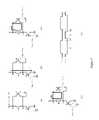
- FIGS. 1 a - cshow schematics of a low-side switch, and current paths for various bias conditions.
- FIGS. 2 a - cshow schematics of a high-side switch, and current paths for various bias conditions.
- FIGS. 3 a - eshow schematics of high-side switches with a MOSFET connected across the inductive load, and current paths for various bias conditions.
- FIGS. 4 a - cshow schematics of a boost-mode power-factor correction circuit and current paths for various bias conditions.
- FIGS. 5 a - dshow schematics of a low-side switch, along with current paths for various bias conditions.
- FIG. 5 eshows a biasing scheme for the switching devices in the circuits of FIGS. 5 a - d.
- FIGS. 6 a - dshow schematics of a high-side switch, along with current paths for various bias conditions.
- FIG. 6 eshows a biasing scheme for the switching devices in the circuits of FIGS. 6 a - d.
- FIG. 7shows a schematic of a low-side switch.
- FIGS. 8 a - dshow schematics of a boost-mode power-factor correction circuit, along with current paths for various bias conditions.
- FIG. 8 eshows a biasing scheme for the switching devices in the circuits of FIGS. 8 a - d.
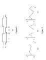
- FIGS. 9 a - cshow the input current as a function of time for various operating conditions for the circuit in FIG. 8 .
- FIGS. 5 a and 6 aLow-side and high-side switches and the circuits which they comprise, wherein the freewheeling diode shown in FIGS. 1-3 is replaced by a switching device, such as a transistor, are described below.
- a switching devicesuch as a transistor
- FIGS. 5 a and 6 athe freewheeling diode used in the circuits of FIGS. 1 and 2 has been replaced by switching device 41 .
- this devicemay be the same as the switching device 42 used to modulate the current path.
- FIGS. 5 b and 6 billustrate the current path when switching device 42 is biased ON (high) and switching device 41 is biased OFF (low).
- FIGS. 5 c and 6 cillustrate the current path when switching device 42 is switched OFF.
- Switching device 41can be an enhancement mode device, where the threshold voltage V th >0, or a depletion mode device, where the threshold voltage V th ⁇ 0.
- enhancement mode deviceswith threshold voltages as large as possible, such as V th >2V or V th >3V, a high internal barrier from source to drain at 0 bias (such as 0.5-2 eV), a high ON-to-OFF current ratio (such as >10 5 ), along with high breakdown voltage (600/1200 Volts) and low on resistance ( ⁇ 5 or ⁇ 10 mohm-cm 2 for 600/1200 V respectively).
- switching device 41must have the following characteristics. It must be able to block significant voltage when the voltage at terminal 45 / 55 is lower than the voltage at terminal 46 / 56 . This condition occurs when switching device 42 is biased high, as shown in FIGS. 5 b and 6 b .
- blocking a voltagerefers to the ability of a transistor to prevent a current that is greater than 0.0001 times the operating current during regular conduction from flowing through the transistor when a voltage is applied across the transistor. In other words, while a transistor is blocking a voltage which is applied across it, the total current passing through the transistor will not be greater than 0.0001 times the operating current during regular conduction.
- substantially currentincludes any current which is at least ten percent of the operating current during regular conduction.
- the maximum voltage that switching device 41 must be able to blockdepends on the particular circuit application, but in general will be the same or very close to the maximum blocking voltage specified for switching device 42 . In some embodiments, switching device 41 is able to block voltage in both directions. When switching device 42 is switched OFF, switching device 41 must be capable of conducting current 13 in the direction shown in FIGS. 5 c and 6 c . Furthermore, when the circuit is biased such as shown in FIG. 5 c or 6 c , all substantial current through switching device 41 flows through a single, primary channel of the device, wherein the conductivity of this channel may be modulated by the gate electrode.
- switching device 42When switching device 42 is biased ON, such as by setting the gate-source voltage V GS42 greater than the device threshold voltage V th42 , and switching device 41 is biased OFF, such as by setting V GS41 ⁇ V th41 , current 13 flows through inductive load 10 and switching device 42 , as seen in FIG. 5 b .
- switching device 41is said to be in “blocking mode”, as it is supporting a voltage across it while at the same time blocking current from flowing through it, i.e., device 41 is blocking voltage. As shown in FIG.
- a lower power mode of operationmay be achieved by applying a voltage V GS41 >V th41 to the gate of switching device 41 , as shown in FIG. 5 d .
- V GS41 >V th41a voltage
- FIG. 5 eTo prevent shoot-through currents from the high-voltage supply (HV) to ground, gate signals of the form shown in FIG. 5 e are applied.
- the time during which switching device 42 is ON and switching device 41 is OFFis labeled “C” in FIG. 5 e . This corresponds to the mode of operation shown in FIG. 5 b .
- switching device 42When switching device 42 is switched OFF, during the time switching device 41 conducts the freewheeling current, the gate of switching device 41 is driven high, allowing the drain-source voltage of switching device 41 to be simply the on-state resistance (R ds-on ) times the load current.
- R ds-onOn-state resistance
- some dead timemust be provided between turn-off of switching device 42 and turn-on of switching device 41 . These are the times labeled “A” in FIG. 5 e .
- switching device 41operates in the diode mode described above. Since this is a short time in comparison with the entire switching cycle, the relative amount of total power dissipation is low.
- Time “B”provides the dominant loss factor for switching device 41 , and this corresponds to the low-power mode when switching device 41 is fully enhanced.
- the mode of operation illustrated in FIG. 5 dallows for a further reduction in conduction loss, although switching losses remain unaffected.
- FIG. 6The detailed operation of the circuit in FIG. 6 is similar to that of FIG. 5 .
- switching device 42When switching device 42 is biased ON, such as by setting V GS42 >V th42 , and switching device 41 is biased OFF, such as by setting V GS41 ⁇ V th41 , current 13 flows through inductive load 10 and switching device 42 , as seen in FIG. 6 b .
- FIG. 6 cwhen switching device 42 is switched OFF, the current through the inductive load 10 cannot change abruptly, so the voltage at terminal 56 is forced sufficiently negative to allow the freewheeling current 13 to be carried through switching device 41 , and switching device 41 now operates in diode mode. Again, in this mode of operation, current is able to flow through switching device 41 even if V GS41 is not changed.
- power dissipation during diode mode operation of switching device 41may be reduced by applying a voltage V GS41 >V th41 to the gate of switching device 41 , as shown in FIG. 6 d .
- V GS41 >V th41a voltage
- some dead timemust be provided between turn-off of switching device 42 and turn-on of switching device 41 in order to avoid shoot-through currents from the high-voltage supply (HV) to ground, and so the bias scheme shown in FIG. 6 e is used.
- Examples of devices that meet the criteria specified above for switching device 41are metal-semiconductor field effect transistors (MESFETs) of any material system, junction field effect transistors (JFETs) of any material system, high electron mobility transistors (HEMTs or HFETs) of any material system, including vertical devices such as current aperture vertical electron transistors (CAVETs), and bidirectional switches comprised of the devices listed above, such as those described U.S. application Ser. No. 12/209,581, filed Sep. 12, 2008, which is hereby incorporated by reference throughout.
- MEFETsmetal-semiconductor field effect transistors
- JFETsjunction field effect transistors
- HEMTs or HFETshigh electron mobility transistors
- CAVETscurrent aperture vertical electron transistors
- Common material systems for HEMTs and MESFETsinclude Ga x Al y In 1-x-y N m As n P 1-m-n or III-V materials, such as III-N materials, III-As materials, and III-P materials.
- Common materials for JFETsinclude III-V materials, SiC, and Si.
- switching device 41is an enhancement mode device to prevent accidental turn on, in order to avoid damage to the device or other circuit components.
- III-Nitride (III-N) devicessuch as III-Nitride HFETs, are especially desirable due to the large blocking voltages that can be achieved with these devices.
- the devicepreferably also exhibits a high access region conductivity (such as sheet resistance ⁇ 750 ohms/square) along with high breakdown voltage (600/1200 Volts) and low on resistance ( ⁇ 5 or ⁇ 10 mohm-cm 2 for 600/1200 V respectively).
- the devicecan also include any of the following: a surface passivation layer, such as SiN, a field plate, such as a slant field plate, and an insulator underneath the gate.
- switching device 41is a SiC JFET.
- switching device 41includes a high-voltage depletion mode (D-mode) device 97 connected to a low-voltage enhancement mode (E-mode) device 96 as shown.
- D-modehigh-voltage depletion mode
- E-modelow-voltage enhancement mode
- This configuration for switching device 41operates similarly to the case when a high-voltage E-mode device is used for switching device 41 .
- D-mode device 97blocks the voltage across the switch. This configuration can be advantageous because high-voltage E-mode devices are typically difficult to fabricate.
- the D-mode device 97is capable of blocking the maximum voltage drop across the switch, which for high-voltage applications can be 600V or 1200V or other suitable blocking voltage required by the application.
- the E-mode device 96can block at least
- the D-mode devicecan block about 1200V and has a threshold voltage of about ⁇ 5V, and the E-mode device blocks at least about 5V, such as at least about 10V.
- D-mode device 97can be a high-voltage III-N HEMT device
- E-mode device 96can be a Si MOS device or a III-N HEMT device.
- diode 99which is a low-loss diode such as Schottky diode, can optionally be connected antiparallel to device 96 , as shown, in order to reduce switching losses by preventing turn-on of the parasitic reverse diode inherent in Si MOSFETs.
- a similar configuration to the one shown for switching device 41 in FIG. 7can also be used for switching device 42 , and the configuration may also be used for switching devices 41 and 42 in the high-side switch of FIG. 6 . More details of the operation of this configuration can be found in U.S. application Ser. No. 12/209,581.
- FIG. 8 aA boost-mode power-factor correction circuit is shown in FIG. 8 a .
- This circuitis similar to that shown in FIG. 4 a , except that diode 11 has been replaced by a switching device 41 connected to a floating gate-drive circuit 72 .
- Switching device 41must meet the same specifications as switching device 41 in FIGS. 5 and 6 .
- the details of operation of this circuitare as follows. When switching device 42 is biased ON and switching device 41 is biased OFF, as seen in FIG. 8 b , current 13 passes through the load 30 and through the switching device 42 .
- the voltage at node 77is kept sufficiently high by the output capacitor 35 so that switching device 41 is in blocking mode, and thereby does not have any substantial current passing through it. As seen in FIG.
- the load currentis negative (flows in the opposite direction through the load) during some portion of the duty cycle. This may occur if there are any inductive or capacitative components leading into the input of this circuit.
- the third, illustrated in FIG. 9 cis the case where the load current approaches zero but then immediately increases again. This mode is known as the “critical mode”.
- switching device 42is switched ON and switching device 41 is switched OFF, as in FIG. 8 b .
- switching device 42is switched OFF, the inductor forces the load current through switching device 41 as shown in FIG. 8 c , and switching device 41 is in diode mode.
- conduction lossescan be reduced by applying a voltage V GS41 >V th41 to the gate of switching device 41 , as shown in FIG. 8 d .
- Some dead timemust be provided between turn-off of switching device 42 and turn-on of switching device 41 in order to prevent the capacitor 35 from discharging through switching devices 42 and 41 , and so the bias scheme shown in FIG. 8 e is used.
- the current in the inductorcan become discontinuous or negative if the energy stored in it is completely transferred, either to the output capacitor or through switching device 42 , before the commencement of the next switching cycle.
- the switching device 41or flyback transistor
- the switching device 41or flyback transistor
- the flyback transistoris between inductor 30 and capacitor 35
- incorrect operationwould result from leaving switching device 41 enhanced after the load current drops to zero, because the current would reverse sign and start discharging the output capacitor.
- the load currentmust be sensed, either directly or indirectly, and if switching device 41 is on, it must be turned off when the current approaches zero.
- switching device 41can be turned off once the current has dropped to 0.1%, 1%, 3%, or 5% of the peak current.
- the third case, the critical modeis essentially the same as the discontinuous mode, with the difference that the switching device 42 turns back on as soon as the load current approaches zero.
- the control circuitis therefore very different from the discontinuous case, but the requirement regarding the switching sequence of the switching devices 42 and 41 is the same.
- the currentmust be sensed to know when it has approached zero, and switching device 41 must be turned off when the current approaches zero.
Landscapes
- Engineering & Computer Science (AREA)
- Physics & Mathematics (AREA)
- Electromagnetism (AREA)
- General Physics & Mathematics (AREA)
- Radar, Positioning & Navigation (AREA)
- Automation & Control Theory (AREA)
- Dc-Dc Converters (AREA)
- Electronic Switches (AREA)
- Power Conversion In General (AREA)
- Inverter Devices (AREA)
Abstract
Description
- This application claims priority to U.S. Provisional Application Ser. No. 61/099,451, filed on Sep. 23, 2008. The disclosure of the prior application is considered part of and is incorporated by reference in the disclosure of this application.
- This invention relates to power switching circuits, specifically ones for which an inductive load is used.
- A single-sided switch is a switching configuration where a switching device is used either to connect the load to a node at a lower potential—a “low-side” switch—or to a node at a higher potential—a “high-side” switch. The low-side configuration is shown in
FIG. 1 a,and the high-side configuration is shown inFIG. 2 a, where the node at higher potential is represented by a high voltage (HV) source and the node at lower potential is represented by a ground terminal. In both cases, when theload 10 is an inductive load, a freewheeling diode11 (sometimes referred to as a flyback diode) is required to provide a path for the freewheeling load current when the switching device is OFF. For example, as seen inFIG. 1 b,when theswitching device 12 is biased high by applying a gate-source voltage Vgsgreater than the device threshold voltage Vth, current13 flows through theload 10 and throughswitching device 12, anddiode 11 is reverse biased such that no significant current passes through it. Whenswitching device 12 is switched to low by applying a gate-source voltage Vgs<Vth, as shown inFIG. 1 c,the current passing through theinductive load 10 cannot terminate abruptly, and so current13 flows through theload 10 and throughdiode 11, while no significant current flows throughswitching device 12. Similar diagrams detailing current flow through the high-side switching configuration when the switch is biased high and when the switch is turned off (switched low) are shown inFIGS. 2 band2c, respectively. - Ideally, the
freewheeling diodes 11 used in the circuits ofFIGS. 1 and 2 have low conduction loss in the ON state as well as good switching characteristics to minimize transient currents during switching, therefore Schottky diodes are commonly used. However, for some applications Schottky diodes cannot support large enough reverse-bias voltages, so high-voltage diodes which exhibit higher conduction and switching losses must be used. Switchingdevices 12, which are usually transistors, may be enhancement mode (normally off, Vth>0), also known as E-mode, or depletion mode (normally on, Vth<0), also known as D-mode, devices. In power circuits, enhancement mode devices are typically used to prevent accidental turn on, in order to avoid damage to the devices or other circuit components. A key issue with the circuits inFIGS. 1 and 2 is that most high voltage diodes typically exhibit high conduction and switching loss. Further, reverse recovery currents in high-voltage PIN diodes add to the losses of the transistor. - An alternative to the configurations illustrated in
FIGS. 1 and 2 is to instead use synchronous rectification, as illustrated inFIGS. 3 a-e.FIG. 3 ais the same asFIG. 2 a, except that a high-voltage metal-oxide-semiconductor (MOS)transistor 61 is included anti-parallel withdiode 11. A standard MOS transistor inherently contains an anti-parallel parasitic diode and can therefore be represented as atransistor 62 anti-parallel to adiode 63, as illustrated inFIG. 3 a. As seen inFIG. 3 b, whenswitching device 12 is biased high andMOS transistor 61 is biased low,MOS transistor 61 anddiode 11 both block a voltage equal to that across the load, so that theentire current 13 flows through theload 10 and throughswitching device 12. Whenswitching device 12 is switched to low, as shown inFIG. 3 c,diode 11 preventstransistor 62 andparasitic diode 63 from turning on by clamping the gate-drain voltage to a value less than Vthof the transistor and less then the turn-on voltage of the parasitic diode. Therefore, almost all of the freewheeling current flows throughdiode 11, while only a small, insignificant portion flows through the transistor channel and parasitic diode. As shown inFIG. 3 d,MOS device 61 may then be biased high, which results in an increase in the channel conductivity oftransistor 62 and thereby cause the majority of the freewheeling current to flow through the transistor channel. However, some dead time must be provided between turn-off of switchingdevice 12 and turn-on oftransistor 62 in order to avoid shoot-through currents from the high-voltage supply (HV) to ground. Therefore,diode 11 will be turned on for some time immediately after switchingdevice 12 is switched from high to low and immediately before switchingdevice 12 is switched back from low to high. While this reduces the conduction losses incurred bydiode 11 in the absence ofMOS transistor 61, the full switching loss fordiode 11 is incurred, regardless of how long the diode remains on. - As shown in
FIG. 3 e, the circuit inFIGS. 3 a-dcan in principle operate withoutdiode 11. In this case,parasitic diode 63 performs the same function thatdiode 11 performed in the circuit ofFIGS. 3 a-d.However, theparasitic diode 63 typically has much poorer switching characteristics and suffers from higher switching losses than a standard high-voltage diode, resulting in increased power loss, so the circuit ofFIGS. 3 a-dis usually preferred. - Many power switching circuits contain one or more high-side or low-side switches. One example is the boost-mode power-factor correction circuit shown in
FIG. 4 a, which contains a low-side switch. This circuit is used at the input end in AC-to-DC voltage conversion circuits. The configuration for the low-side switch in this circuit is slightly modified from that shown inFIG. 1 a,since inFIG. 1 athefreewheeling diode 11 is connected anti-parallel to theinductive load 10, whereas in this circuit thefreewheeling diode 11 is between theinductive load 30 and theoutput capacitor 35. However, the fundamental operating principles of the two circuits are the same. As seen inFIG. 4 b, when switchingdevice 12 is biased high, current13 passes through theload 30 and through theswitching device 12. The voltage at the cathode end of thefreewheeling diode 11 is kept sufficiently high by theoutput capacitor 35 so that thefreewheeling diode 11 is reverse-biased, and thereby does not have any significant current passing through it. As seen inFIG. 4 c, when switchingdevice 12 is switched low, the inductor forces the voltage at the anode of thefreewheeling diode 11 to be sufficiently high such that thefreewheeling diode 11 is forward biased, and the current13 then flows through theinductive load 30, thefreewheeling diode 11, and theoutput capacitor 35. Because no significant current can flow in the reverse direction in a diode,diode 11 prevents discharge of theoutput capacitor 35 throughswitching device 12 during times where the load current is zero or negative, as can occur if the energy stored in theinductor 30 is completely transferred out before the commencement of the next switching cycle. - In one aspect, a switch is described that includes a first switching device in series with an assembly comprising a load and a second switching device, the first switching device including a first channel, the second switching device including a second channel, wherein in a first mode of operation the second switching device is capable of blocking a voltage applied across the second switching device in a first direction, in a second mode of operation a substantial current flows through the second channel of the second switching device when a voltage is applied across the second switching device in a second direction and a gate of the second switching device is biased below a threshold voltage of the second switching device, and in a third mode of operation a substantial current flows through the second channel of the second switching device when a voltage is applied across the second switching device in the second direction and the gate of the second switching device is biased above the threshold voltage of the second switching device.
- The switch or the assembly can be free of any diodes.
- In another aspect, a method of operating a switch is described. At a first time, a gate of a first switching device of a switch is biased higher than a threshold voltage of the first switching device and a gate of a second switching device is biased lower than a threshold voltage of the second switching device, allowing current to flow from a high voltage side of the switch to a low voltage or ground side of the switch through the load. At a second time immediately following the first time, a bias on the gate of the first switching device is changed to be lower than the threshold voltage of the first switching device, causing the second switching device to operate in diode mode and blocking current from flowing to ground. At a third time immediately following the second time, a bias on the gate of the second switching device is changed to be higher than the threshold voltage of the second switching device, wherein changing the bias at the third time reduces conduction loss in comparison to switch operation between the second time and the third time.
- In another aspect, a boost-mode power-factor correction circuit is described. The circuit includes a first switching device comprising a first channel, an inductive load, a capacitor, and a second switching device comprising a second channel, wherein the first switching device is connected to a node between the inductive load and a floating gate drive circuit, the second switching device is configured to be connected to the floating gate drive circuit, and the second switching device is between the inductive load and the capacitor.
- In yet another aspect, a method of operating the boost-mode power-factor correction circuit is described. The method includes causing a load current through the inductive load to be continuous; at a first time, biasing a gate of the first switching device higher than a threshold voltage of the first switching device and biasing a gate of the second switching device lower than a threshold voltage of the second switching device, allowing current to flow through the first switching device; at a second time immediately following the first time, changing a bias on the gate of the first switching device to be lower than the threshold voltage of the first switching device, causing the first switching device to operate in blocking mode and the second switching device to operate in diode mode, allowing current to flow through the second switching device; at a third time immediately following the second time, changing a bias on the gate of the second switching device to be higher than the threshold voltage of the second switching device, wherein changing the bias at the third time reduces conduction loss in comparison to switch operation between the second time and the third time.
- In another aspect, a method of operating the boost-mode power-factor correction circuit is described. The method includes causing a load current through the inductive load to be discontinuous, sensing the load current, and when the load current approaches zero, changing a bias on a gate of the second switching device from a voltage higher than a threshold voltage of the second switching device to a voltage lower than the threshold voltage of the second switching.
- In yet another aspect a method of operating the boost-mode power-factor correction circuit is described. The method includes sensing a load current passing through the inductive load, causing the load current to approach zero and immediately increase after approaching zero, and when the load current approaches zero, switching the second switching device from on to off and switching the first switching device from off to on.
- In some embodiments, the following features are present. The first mode of operation can comprise biasing the gate of the first switching device above a threshold voltage of the first switching device. The second mode of operation can comprise biasing the gate of the first switching device below a threshold voltage of the first switching device. The first switching device can have a first terminal and a second terminal on opposite sides of the gate, and the first terminal can be adjacent to the assembly and at a higher voltage than the second terminal of the first switching device during operation. The first switching device can have a first terminal and a second terminal on opposite sides of the gate, and the first terminal can be adjacent to the assembly and at a lower voltage than the second terminal of the first switching device during operation. A first node can be between the assembly and the first switching device, a second node can be at a high voltage side of the switch, and the second switching device can be capable of blocking a voltage when voltage at the first node is lower than voltage at the second node. A first node can be between the assembly and the first switching device, a second node can be at a low voltage or ground side of the switch, and the second switching device can be capable of blocking a voltage when voltage at the first node is higher than voltage at the second node. The second switching device can be capable of blocking a same voltage as the first switching device is capable of blocking The second switching device can be capable of blocking voltage in two directions. When the gate of the first switching device is biased lower than a threshold voltage of the first switching device, the second switching device can be capable of conducting current. When the gate of the first switching device is biased lower than the threshold voltage of the first switching device, substantially all current can flow through a single primary channel of the second switching device. When the gate of the second switching device is biased higher than the threshold voltage of the second switching device, the voltage drop across the second switching device can be reduced as compared to when the gate of the second switching device is biased lower than the threshold voltage of the second switching device. The second switching device can have a positive threshold voltage. The first switching device can have a positive threshold voltage. The second switching device can be a HEMT. The second switching device can be a III-Nitride HEMT. The first switching device can be a HEMT. The first switching device can be a III-Nitride HEMT. The second switching device can be structurally the same as the first switching device. A voltage drop across the second switching device can be smaller in the third mode of operation as compared to in the second mode of operation. The load can be an inductive load. The first switching device or the second switching device can comprise a high-voltage depletion mode device and a low-voltage enhancement mode device, the second channel can be a channel of the high-voltage depletion mode device, and the threshold voltage of the second switching device can be a threshold voltage of the low-voltage enhancement mode device. The low-voltage enhancement mode device can at least block a voltage equal to an absolute value of a threshold voltage of the high-voltage depletion mode device. The high-voltage depletion mode device can be a III-Nitride HEMT. The low-voltage enhancement mode device can be a III-Nitride HEMT. The low-voltage enhancement mode device can be a Si MOS device. The device can include a diode connected antiparallel to the low-voltage enhancement mode device. The first switching device can comprise a high-voltage depletion mode device and a low-voltage enhancement mode device, the first channel can be a channel of the high-voltage depletion mode device, and a threshold voltage of the first switching device can be a threshold voltage of the low-voltage enhancement mode device.
- Boost-mode power-factor correction circuits can include one or more of the following features. The first switching device can be a III-N HEMT. The second switching device can be a III-N HEMT.
- Operating a boost-mode power-factor correction circuit can include causing a load current through the inductive load to be discontinuous, sensing the load current, and when the load current approaches zero, changing a bias on a gate of the second switching device from a voltage higher than a threshold voltage of the second switching device to a voltage lower than the threshold voltage of the second switching device. A load current passing through the inductive load, causing the load current to approach zero and immediately increase after approaching zero is sensed. When the load current approaches zero, the second switching device is switched from on to off and the first switching device is switched from off to on.
- Methods described herein may include one or more of the following features or steps. Changing the bias at the third time can reduce conduction loss in comparison to switch operation at the second time.
FIGS. 1 a-cshow schematics of a low-side switch, and current paths for various bias conditions.FIGS. 2 a-cshow schematics of a high-side switch, and current paths for various bias conditions.FIGS. 3 a-eshow schematics of high-side switches with a MOSFET connected across the inductive load, and current paths for various bias conditions.FIGS. 4 a-cshow schematics of a boost-mode power-factor correction circuit and current paths for various bias conditions.FIGS. 5 a-dshow schematics of a low-side switch, along with current paths for various bias conditions.FIG. 5 eshows a biasing scheme for the switching devices in the circuits ofFIGS. 5 a-d.FIGS. 6 a-dshow schematics of a high-side switch, along with current paths for various bias conditions.FIG. 6 eshows a biasing scheme for the switching devices in the circuits ofFIGS. 6 a-d.FIG. 7 shows a schematic of a low-side switch.FIGS. 8 a-dshow schematics of a boost-mode power-factor correction circuit, along with current paths for various bias conditions.FIG. 8 eshows a biasing scheme for the switching devices in the circuits ofFIGS. 8 a-d.FIGS. 9 a-cshow the input current as a function of time for various operating conditions for the circuit inFIG. 8 .- Low-side and high-side switches and the circuits which they comprise, wherein the freewheeling diode shown in
FIGS. 1-3 is replaced by a switching device, such as a transistor, are described below. Embodiments are shown inFIGS. 5 aand6a, whereinFIG. 5 acomprises a low-side switch, andFIG. 6 acomprises a high-side switch. InFIGS. 5 aand6a, the freewheeling diode used in the circuits ofFIGS. 1 and 2 has been replaced by switchingdevice 41. In some embodiments, this device may be the same as the switchingdevice 42 used to modulate the current path.FIGS. 5 band6billustrate the current path when switchingdevice 42 is biased ON (high) and switchingdevice 41 is biased OFF (low).FIGS. 5 cand6cillustrate the current path when switchingdevice 42 is switched OFF.Switching device 41 can be an enhancement mode device, where the threshold voltage Vth>0, or a depletion mode device, where the threshold voltage Vth<0. In high power applications, it is desirable to use enhancement mode devices with threshold voltages as large as possible, such as Vth>2V or Vth>3V, a high internal barrier from source to drain at 0 bias (such as 0.5-2 eV), a high ON-to-OFF current ratio (such as >105), along with high breakdown voltage (600/1200 Volts) and low on resistance (<5 or <10 mohm-cm2for 600/1200 V respectively). - Additionally, switching
device 41 must have the following characteristics. It must be able to block significant voltage when the voltage atterminal 45/55 is lower than the voltage atterminal 46/56. This condition occurs when switchingdevice 42 is biased high, as shown inFIGS. 5 band6b. As used herein, “blocking a voltage” refers to the ability of a transistor to prevent a current that is greater than 0.0001 times the operating current during regular conduction from flowing through the transistor when a voltage is applied across the transistor. In other words, while a transistor is blocking a voltage which is applied across it, the total current passing through the transistor will not be greater than 0.0001 times the operating current during regular conduction. As used herein, “substantial current” includes any current which is at least ten percent of the operating current during regular conduction. The maximum voltage that switchingdevice 41 must be able to block depends on the particular circuit application, but in general will be the same or very close to the maximum blocking voltage specified for switchingdevice 42. In some embodiments, switchingdevice 41 is able to block voltage in both directions. When switchingdevice 42 is switched OFF, switchingdevice 41 must be capable of conducting current13 in the direction shown inFIGS. 5 cand6c. Furthermore, when the circuit is biased such as shown inFIG. 5 cor6c, all substantial current through switchingdevice 41 flows through a single, primary channel of the device, wherein the conductivity of this channel may be modulated by the gate electrode. This is different from the circuits inFIGS. 3 a-3e,for which applying a voltage signal to the gate electrode ofdevice 61 causes the current to shift from one channel (that ofdiode 11 or63) to that of thetransistor 62. The maximum current that switchingdevice 41 must be able to conduct in this direction depends on the particular circuit application, but in general will be the same or very close to the maximum current specified for switchingdevice 42. In some embodiments, the switching devices are able to conduct current in both directions. - The detailed operation of the circuit in
FIG. 5 is as follows. When switchingdevice 42 is biased ON, such as by setting the gate-source voltage VGS42greater than the device threshold voltage Vth42, and switchingdevice 41 is biased OFF, such as by setting VGS41<Vth41, current13 flows throughinductive load 10 and switchingdevice 42, as seen inFIG. 5 b. Here, switchingdevice 41 is said to be in “blocking mode”, as it is supporting a voltage across it while at the same time blocking current from flowing through it, i.e.,device 41 is blocking voltage. As shown inFIG. 5 c, when switchingdevice 42 is switched OFF, the current through theinductive load 10 cannot change abruptly, so the voltage atterminal 45 is forced sufficiently high to allow the freewheeling current13 to be carried through switchingdevice 41. Note that in this mode of operation, current is able to flow through switchingdevice 41 even if VGS41is not changed. This mode of operation for switchingdevice 41 is known as “diode mode operation”. The circuit ofFIG. 5 may be preferable to that ofFIG. 1 because transistors suitable for use in this application typically have lower conduction and switching losses thandiode 11. - Depending on the current level and the threshold voltage of switching
device 41, the power dissipation through this device could be unacceptably high when operating in the diode mode. In this case, a lower power mode of operation may be achieved by applying a voltage VGS41>Vth41to the gate of switchingdevice 41, as shown inFIG. 5 d. To prevent shoot-through currents from the high-voltage supply (HV) to ground, gate signals of the form shown inFIG. 5 eare applied. The time during whichswitching device 42 is ON and switchingdevice 41 is OFF is labeled “C” inFIG. 5 e. This corresponds to the mode of operation shown inFIG. 5 b. When switchingdevice 42 is switched OFF, during thetime switching device 41 conducts the freewheeling current, the gate of switchingdevice 41 is driven high, allowing the drain-source voltage of switchingdevice 41 to be simply the on-state resistance (Rds-on) times the load current. To avoid shoot-through currents from the high-voltage supply (HV) to ground, some dead time must be provided between turn-off of switchingdevice 42 and turn-on of switchingdevice 41. These are the times labeled “A” inFIG. 5 e. During these dead times, switchingdevice 41 operates in the diode mode described above. Since this is a short time in comparison with the entire switching cycle, the relative amount of total power dissipation is low. Time “B” provides the dominant loss factor for switchingdevice 41, and this corresponds to the low-power mode when switchingdevice 41 is fully enhanced. The mode of operation illustrated inFIG. 5 dallows for a further reduction in conduction loss, although switching losses remain unaffected. - In the circuit of
FIG. 5 , when switchingdevice 42 is switched OFF, all substantial current flows through the primary channel of switchingdevice 41 when the gate of switchingdevice 41 remains low (FIG. 5 c) as well as when it is driven high (FIG. 5 d). This may be preferable to the operation of the circuit inFIG. 3 , for which substantial current initially flows through a diode whiletransistor 61 remains low and only flows through the primary transistor channel once the gate oftransistor 61 is driven high.Diode 11 andparasitic diode 63 inFIG. 3 typically exhibit higher switching losses thantransistors 41 suitable for use in the circuit ofFIG. 5 . Additionally, switchingdevices FIG. 5 can be identical or similar devices, which simplifies the fabrication of this circuit. - The detailed operation of the circuit in
FIG. 6 is similar to that ofFIG. 5 . When switchingdevice 42 is biased ON, such as by setting VGS42>Vth42, and switchingdevice 41 is biased OFF, such as by setting VGS41<Vth41, current13 flows throughinductive load 10 and switchingdevice 42, as seen inFIG. 6 b. As shown inFIG. 6 c, when switchingdevice 42 is switched OFF, the current through theinductive load 10 cannot change abruptly, so the voltage atterminal 56 is forced sufficiently negative to allow the freewheeling current13 to be carried through switchingdevice 41, and switchingdevice 41 now operates in diode mode. Again, in this mode of operation, current is able to flow through switchingdevice 41 even if VGS41is not changed. As with the circuit ofFIG. 5 , power dissipation during diode mode operation of switchingdevice 41 may be reduced by applying a voltage VGS41>Vth41to the gate of switchingdevice 41, as shown inFIG. 6 d. Again, some dead time must be provided between turn-off of switchingdevice 42 and turn-on of switchingdevice 41 in order to avoid shoot-through currents from the high-voltage supply (HV) to ground, and so the bias scheme shown inFIG. 6 eis used. - Examples of devices that meet the criteria specified above for switching
device 41 are metal-semiconductor field effect transistors (MESFETs) of any material system, junction field effect transistors (JFETs) of any material system, high electron mobility transistors (HEMTs or HFETs) of any material system, including vertical devices such as current aperture vertical electron transistors (CAVETs), and bidirectional switches comprised of the devices listed above, such as those described U.S. application Ser. No. 12/209,581, filed Sep. 12, 2008, which is hereby incorporated by reference throughout. Common material systems for HEMTs and MESFETs include GaxAlyIn1-x-yNmAsnP1-m-nor III-V materials, such as III-N materials, III-As materials, and III-P materials. Common materials for JFETs include III-V materials, SiC, and Si. - Preferably, switching
device 41 is an enhancement mode device to prevent accidental turn on, in order to avoid damage to the device or other circuit components. III-Nitride (III-N) devices, such as III-Nitride HFETs, are especially desirable due to the large blocking voltages that can be achieved with these devices. The device preferably also exhibits a high access region conductivity (such as sheet resistance <750 ohms/square) along with high breakdown voltage (600/1200 Volts) and low on resistance (<5 or <10 mohm-cm2for 600/1200 V respectively). The device can also include any of the following: a surface passivation layer, such as SiN, a field plate, such as a slant field plate, and an insulator underneath the gate. In other embodiments, switchingdevice 41 is a SiC JFET. - A variation on switching
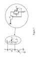
device 41, which can be used with any of the embodiments described herein, embodiment is shown inFIG. 7 . In this embodiment, switchingdevice 41 includes a high-voltage depletion mode (D-mode)device 97 connected to a low-voltage enhancement mode (E-mode)device 96 as shown. This configuration for switchingdevice 41 operates similarly to the case when a high-voltage E-mode device is used for switchingdevice 41. When the voltage atnode 46 is higher than that atnode 45 and the gate ofE-mode device 96 is biased at 0V or below the threshold voltage ofE-mode device 96, D-mode device 97 blocks the voltage across the switch. This configuration can be advantageous because high-voltage E-mode devices are typically difficult to fabricate. The D-mode device 97 is capable of blocking the maximum voltage drop across the switch, which for high-voltage applications can be 600V or 1200V or other suitable blocking voltage required by the application. Typical D-mode device threshold voltages for high-voltage devices are about −5 to −10V (D-mode=negative Vth). TheE-mode device 96 can block at least |Vth|, where |Vth| is the magnitude (absolute value) of the threshold voltage of the D-mode device. In some embodiments the E-mode device can block about 2*|Vth|. In some embodiments, the D-mode device can block about 1200V and has a threshold voltage of about −5V, and the E-mode device blocks at least about 5V, such as at least about 10V. D-mode device 97 can be a high-voltage III-N HEMT device, andE-mode device 96 can be a Si MOS device or a III-N HEMT device. When a Si MOS device is used fordevice 96, diode99, which is a low-loss diode such as Schottky diode, can optionally be connected antiparallel todevice 96, as shown, in order to reduce switching losses by preventing turn-on of the parasitic reverse diode inherent in Si MOSFETs. A similar configuration to the one shown for switchingdevice 41 inFIG. 7 can also be used for switchingdevice 42, and the configuration may also be used for switchingdevices FIG. 6 . More details of the operation of this configuration can be found in U.S. application Ser. No. 12/209,581. - A boost-mode power-factor correction circuit is shown in
FIG. 8 a. This circuit is similar to that shown inFIG. 4 a, except thatdiode 11 has been replaced by aswitching device 41 connected to a floating gate-drive circuit 72.Switching device 41 must meet the same specifications as switchingdevice 41 inFIGS. 5 and 6 . The details of operation of this circuit are as follows. When switchingdevice 42 is biased ON and switchingdevice 41 is biased OFF, as seen inFIG. 8 b, current13 passes through theload 30 and through the switchingdevice 42. The voltage atnode 77 is kept sufficiently high by theoutput capacitor 35 so that switchingdevice 41 is in blocking mode, and thereby does not have any substantial current passing through it. As seen inFIG. 8 c, when switchingdevice 42 is switched OFF, the inductor forces the voltage atnode 76 to be sufficiently high such that switchingdevice 41 switches to diode mode, and the current13 then flows through theinductive load 30, switchingdevice 41, and theoutput capacitor 35. - As with the circuits in
FIGS. 5 and 6 , conduction losses in this circuit can be reduced by applying a voltage VGS41>Vth41to the gate of switchingdevice 41, as shown inFIG. 8 d. However, for this circuit to operate properly, the timing of the signals applied by gate-drive circuit 72 to the gate of switchingdevice 41 must be properly controlled. There are three cases which need to be considered independently. The first, illustrated inFIG. 9 a, is the case where the load current is continuous (continuous mode). The second, illustrated isFIG. 9 b, is the case where the load current is discontinuous (discontinuous mode), such that no current flows during some portion of the duty cycle. For this second case, it is also possible that the load current is negative (flows in the opposite direction through the load) during some portion of the duty cycle. This may occur if there are any inductive or capacitative components leading into the input of this circuit. The third, illustrated inFIG. 9 c, is the case where the load current approaches zero but then immediately increases again. This mode is known as the “critical mode”. - If the load current is continuous, then the timing of the gate signals to switching
devices FIGS. 5 and 6 . To allow the load current to flow through switchingdevice 42, switchingdevice 42 is switched ON and switchingdevice 41 is switched OFF, as inFIG. 8 b. When switchingdevice 42 is switched OFF, the inductor forces the load current through switchingdevice 41 as shown inFIG. 8 c, and switchingdevice 41 is in diode mode. While current flows through switchingdevice 41, conduction losses can be reduced by applying a voltage VGS41>Vth41to the gate of switchingdevice 41, as shown inFIG. 8 d. Some dead time must be provided between turn-off of switchingdevice 42 and turn-on of switchingdevice 41 in order to prevent thecapacitor 35 from discharging through switchingdevices FIG. 8 eis used. - The current in the inductor can become discontinuous or negative if the energy stored in it is completely transferred, either to the output capacitor or through switching
device 42, before the commencement of the next switching cycle. In circuits where theswitching device 41, or flyback transistor, is connected in parallel to the load, such as those inFIGS. 5 and 6 , there is no harm in leaving the flyback transistor enhanced even after the load current has dropped to zero. However, in the power factor correction circuit ofFIG. 8 , where the flyback transistor is betweeninductor 30 andcapacitor 35, incorrect operation would result from leavingswitching device 41 enhanced after the load current drops to zero, because the current would reverse sign and start discharging the output capacitor. In such a system, the load current must be sensed, either directly or indirectly, and if switchingdevice 41 is on, it must be turned off when the current approaches zero. For example, switchingdevice 41 can be turned off once the current has dropped to 0.1%, 1%, 3%, or 5% of the peak current. - The third case, the critical mode, is essentially the same as the discontinuous mode, with the difference that the switching
device 42 turns back on as soon as the load current approaches zero. This implies that the switching frequency is not fixed, but adjustable, as in a hysteretic controller. The control circuit is therefore very different from the discontinuous case, but the requirement regarding the switching sequence of theswitching devices device 41 must be turned off when the current approaches zero.
Claims (38)
Priority Applications (9)
| Application Number | Priority Date | Filing Date | Title |
|---|---|---|---|
| US12/556,438US8289065B2 (en) | 2008-09-23 | 2009-09-09 | Inductive load power switching circuits |
| CN201410214282.5ACN104300947B (en) | 2008-09-23 | 2009-09-18 | Inductive load power switching circuits |
| CN200980137436.2ACN102165694B (en) | 2008-09-23 | 2009-09-18 | Inductive load power switch circuit |
| PCT/US2009/057554WO2010039463A2 (en) | 2008-09-23 | 2009-09-18 | Inductive load power switching circuits |
| TW098132132ATWI431936B (en) | 2008-09-23 | 2009-09-23 | Inductive load power switching circuits and operating method thereof |
| US13/618,502US8493129B2 (en) | 2008-09-23 | 2012-09-14 | Inductive load power switching circuits |
| US13/618,726US8531232B2 (en) | 2008-09-23 | 2012-09-14 | Inductive load power switching circuits |
| US13/959,483US8816751B2 (en) | 2008-09-23 | 2013-08-05 | Inductive load power switching circuits |
| US14/332,967US9690314B2 (en) | 2008-09-23 | 2014-07-16 | Inductive load power switching circuits |
Applications Claiming Priority (2)
| Application Number | Priority Date | Filing Date | Title |
|---|---|---|---|
| US9945108P | 2008-09-23 | 2008-09-23 | |
| US12/556,438US8289065B2 (en) | 2008-09-23 | 2009-09-09 | Inductive load power switching circuits |
Related Child Applications (2)
| Application Number | Title | Priority Date | Filing Date |
|---|---|---|---|
| US13/618,502DivisionUS8493129B2 (en) | 2008-09-23 | 2012-09-14 | Inductive load power switching circuits |
| US13/618,726ContinuationUS8531232B2 (en) | 2008-09-23 | 2012-09-14 | Inductive load power switching circuits |
Publications (2)
| Publication Number | Publication Date |
|---|---|
| US20100073067A1true US20100073067A1 (en) | 2010-03-25 |
| US8289065B2 US8289065B2 (en) | 2012-10-16 |
Family
ID=42037005
Family Applications (5)
| Application Number | Title | Priority Date | Filing Date |
|---|---|---|---|
| US12/556,438Active2030-01-13US8289065B2 (en) | 2008-09-23 | 2009-09-09 | Inductive load power switching circuits |
| US13/618,726ActiveUS8531232B2 (en) | 2008-09-23 | 2012-09-14 | Inductive load power switching circuits |
| US13/618,502ActiveUS8493129B2 (en) | 2008-09-23 | 2012-09-14 | Inductive load power switching circuits |
| US13/959,483ActiveUS8816751B2 (en) | 2008-09-23 | 2013-08-05 | Inductive load power switching circuits |
| US14/332,967Active2030-09-05US9690314B2 (en) | 2008-09-23 | 2014-07-16 | Inductive load power switching circuits |
Family Applications After (4)
| Application Number | Title | Priority Date | Filing Date |
|---|---|---|---|
| US13/618,726ActiveUS8531232B2 (en) | 2008-09-23 | 2012-09-14 | Inductive load power switching circuits |
| US13/618,502ActiveUS8493129B2 (en) | 2008-09-23 | 2012-09-14 | Inductive load power switching circuits |
| US13/959,483ActiveUS8816751B2 (en) | 2008-09-23 | 2013-08-05 | Inductive load power switching circuits |
| US14/332,967Active2030-09-05US9690314B2 (en) | 2008-09-23 | 2014-07-16 | Inductive load power switching circuits |
Country Status (4)
| Country | Link |
|---|---|
| US (5) | US8289065B2 (en) |
| CN (2) | CN102165694B (en) |
| TW (1) | TWI431936B (en) |
| WO (1) | WO2010039463A2 (en) |
Cited By (17)
| Publication number | Priority date | Publication date | Assignee | Title |
|---|---|---|---|---|
| US20110049526A1 (en)* | 2009-08-28 | 2011-03-03 | Transphorm Inc. | Semiconductor Devices with Field Plates |
| US20110169549A1 (en)* | 2010-01-08 | 2011-07-14 | Transphorm Inc. | Electronic devices and components for high efficiency power circuits |
| US20110193619A1 (en)* | 2010-02-05 | 2011-08-11 | Transphorm Inc. | Semiconductor electronic components and circuits |
| WO2012009410A1 (en) | 2010-07-15 | 2012-01-19 | Cree, Inc. | Power converter circuits including high electron mobility transistors for switching and rectification |
| US8289065B2 (en) | 2008-09-23 | 2012-10-16 | Transphorm Inc. | Inductive load power switching circuits |
| US8344424B2 (en) | 2007-09-17 | 2013-01-01 | Transphorm Inc. | Enhancement mode gallium nitride power devices |
| US8455931B2 (en) | 2009-11-02 | 2013-06-04 | Transphorm Inc. | Package configurations for low EMI circuits |
| US8508281B2 (en) | 2008-02-12 | 2013-08-13 | Transphorm Inc. | Bridge circuits and their components |
| US20140021934A1 (en)* | 2012-07-17 | 2014-01-23 | Transphorm, Inc. | Devices and components for power conversion circuits |
| US8648643B2 (en) | 2012-02-24 | 2014-02-11 | Transphorm Inc. | Semiconductor power modules and devices |
| US8786327B2 (en) | 2011-02-28 | 2014-07-22 | Transphorm Inc. | Electronic components with reactive filters |
| US8803246B2 (en) | 2012-07-16 | 2014-08-12 | Transphorm Inc. | Semiconductor electronic components with integrated current limiters |
| US20150116007A1 (en)* | 2012-12-17 | 2015-04-30 | Continental Automotive Systems Us, Inc. | Voltage clamp assist circuit |
| US9059076B2 (en) | 2013-04-01 | 2015-06-16 | Transphorm Inc. | Gate drivers for circuits based on semiconductor devices |
| US9209176B2 (en) | 2011-12-07 | 2015-12-08 | Transphorm Inc. | Semiconductor modules and methods of forming the same |
| US9484418B2 (en) | 2012-11-19 | 2016-11-01 | Delta Electronics, Inc. | Semiconductor device |
| US11506715B2 (en) | 2018-07-17 | 2022-11-22 | Lg Energy Solution, Ltd. | Switch diagnosing apparatus and method |
Families Citing this family (40)
| Publication number | Priority date | Publication date | Assignee | Title |
|---|---|---|---|---|
| US8519438B2 (en) | 2008-04-23 | 2013-08-27 | Transphorm Inc. | Enhancement mode III-N HEMTs |
| US7898004B2 (en) | 2008-12-10 | 2011-03-01 | Transphorm Inc. | Semiconductor heterostructure diodes |
| US8742459B2 (en) | 2009-05-14 | 2014-06-03 | Transphorm Inc. | High voltage III-nitride semiconductor devices |
| US8389977B2 (en) | 2009-12-10 | 2013-03-05 | Transphorm Inc. | Reverse side engineered III-nitride devices |
| US8742460B2 (en) | 2010-12-15 | 2014-06-03 | Transphorm Inc. | Transistors with isolation regions |
| US8643062B2 (en) | 2011-02-02 | 2014-02-04 | Transphorm Inc. | III-N device structures and methods |
| US8772842B2 (en) | 2011-03-04 | 2014-07-08 | Transphorm, Inc. | Semiconductor diodes with low reverse bias currents |
| US8716141B2 (en) | 2011-03-04 | 2014-05-06 | Transphorm Inc. | Electrode configurations for semiconductor devices |
| US8598937B2 (en) | 2011-10-07 | 2013-12-03 | Transphorm Inc. | High power semiconductor electronic components with increased reliability |
| EP2608357B1 (en)* | 2011-12-19 | 2014-07-23 | Vetco Gray Controls Limited | Protecting against transients in a communication system |
| US9165766B2 (en) | 2012-02-03 | 2015-10-20 | Transphorm Inc. | Buffer layer structures suited for III-nitride devices with foreign substrates |
| WO2013155108A1 (en) | 2012-04-09 | 2013-10-17 | Transphorm Inc. | N-polar iii-nitride transistors |
| US9184275B2 (en) | 2012-06-27 | 2015-11-10 | Transphorm Inc. | Semiconductor devices with integrated hole collectors |
| CN103684415A (en)* | 2012-09-06 | 2014-03-26 | 上海航天控制工程研究所 | Highly reliable inductive load driving technology for spacecraft |
| CN105164811B (en) | 2013-02-15 | 2018-08-31 | 创世舫电子有限公司 | Electrode of semiconductor devices and forming method thereof |
| US9087718B2 (en) | 2013-03-13 | 2015-07-21 | Transphorm Inc. | Enhancement-mode III-nitride devices |
| US9245992B2 (en) | 2013-03-15 | 2016-01-26 | Transphorm Inc. | Carbon doping semiconductor devices |
| US8917135B2 (en)* | 2013-05-14 | 2014-12-23 | Infineon Technologies Austria Ag | Circuit with a plurality of diodes and method for controlling such a circuit |
| JP6201422B2 (en)* | 2013-05-22 | 2017-09-27 | 富士電機株式会社 | Semiconductor device |
| US9537425B2 (en) | 2013-07-09 | 2017-01-03 | Transphorm Inc. | Multilevel inverters and their components |
| US9443938B2 (en) | 2013-07-19 | 2016-09-13 | Transphorm Inc. | III-nitride transistor including a p-type depleting layer |
| US9443787B2 (en) | 2013-08-09 | 2016-09-13 | Infineon Technologies Austria Ag | Electronic component and method |
| US9543940B2 (en) | 2014-07-03 | 2017-01-10 | Transphorm Inc. | Switching circuits having ferrite beads |
| US9590494B1 (en) | 2014-07-17 | 2017-03-07 | Transphorm Inc. | Bridgeless power factor correction circuits |
| US9318593B2 (en) | 2014-07-21 | 2016-04-19 | Transphorm Inc. | Forming enhancement mode III-nitride devices |
| RU2562778C1 (en)* | 2014-12-02 | 2015-09-10 | Федеральное государственное бюджетное образовательное учреждение высшего профессионального образования "Алтайский государственный технический университет им. И.И. Ползунова" (АлтГТУ) | Reversible semiconductor switching device operating for inductive load |
| US9536966B2 (en) | 2014-12-16 | 2017-01-03 | Transphorm Inc. | Gate structures for III-N devices |
| US9536967B2 (en) | 2014-12-16 | 2017-01-03 | Transphorm Inc. | Recessed ohmic contacts in a III-N device |
| US9627962B2 (en)* | 2015-03-09 | 2017-04-18 | Texas Instruments Incorporated | Fast blocking switch |
| WO2016149146A1 (en) | 2015-03-13 | 2016-09-22 | Transphorm, Inc. | Paralleling of switching devices for high power circuits |
| US11322599B2 (en) | 2016-01-15 | 2022-05-03 | Transphorm Technology, Inc. | Enhancement mode III-nitride devices having an Al1-xSixO gate insulator |
| TWI762486B (en) | 2016-05-31 | 2022-05-01 | 美商創世舫科技有限公司 | Iii-nitride devices including a graded depleting layer |
| US10374591B2 (en)* | 2017-01-03 | 2019-08-06 | General Electric Company | Systems and methods for a gate drive circuit |
| US10319648B2 (en) | 2017-04-17 | 2019-06-11 | Transphorm Inc. | Conditions for burn-in of high power semiconductors |
| US10630285B1 (en) | 2017-11-21 | 2020-04-21 | Transphorm Technology, Inc. | Switching circuits having drain connected ferrite beads |
| US10756207B2 (en) | 2018-10-12 | 2020-08-25 | Transphorm Technology, Inc. | Lateral III-nitride devices including a vertical gate module |
| EP3942609A4 (en) | 2019-03-21 | 2023-06-07 | Transphorm Technology, Inc. | INTEGRATED DESIGN FOR NITRIDE III DEVICES |
| US11664741B2 (en) | 2019-07-25 | 2023-05-30 | Susan Rhodes | System and method for AC power control |
| US11749656B2 (en) | 2020-06-16 | 2023-09-05 | Transphorm Technology, Inc. | Module configurations for integrated III-Nitride devices |
| WO2022031465A1 (en) | 2020-08-05 | 2022-02-10 | Transphorm Technology, Inc. | Iii-nitride devices including a depleting layer |
Citations (66)
| Publication number | Priority date | Publication date | Assignee | Title |
|---|---|---|---|---|
| US4728826A (en)* | 1986-03-19 | 1988-03-01 | Siemens Aktiengesellschaft | MOSFET switch with inductive load |
| US5998810A (en)* | 1994-12-19 | 1999-12-07 | Kabushiki Kaisha Toshiba | Semiconductor light-emitting diode having a p-type semiconductor layer formed on a light-emitting layer |
| US6008684A (en)* | 1996-10-23 | 1999-12-28 | Industrial Technology Research Institute | CMOS output buffer with CMOS-controlled lateral SCR devices |
| US20010040247A1 (en)* | 2000-03-28 | 2001-11-15 | Yuji Ando | Hetero-junction field effect transistor having an intermediate layer |
| US6475889B1 (en)* | 2000-04-11 | 2002-11-05 | Cree, Inc. | Method of forming vias in silicon carbide and resulting devices and circuits |
| US20020167023A1 (en)* | 2001-05-11 | 2002-11-14 | Cree Lighting Company And Regents Of The University Of California | Group-III nitride based high electron mobility transistor (HEMT) with barrier/spacer layer |
| US6486502B1 (en)* | 1998-06-12 | 2002-11-26 | Cree, Inc. | Nitride based transistors on semi-insulating silicon carbide substrates |
| US6548333B2 (en)* | 2000-12-01 | 2003-04-15 | Cree, Inc. | Aluminum gallium nitride/gallium nitride high electron mobility transistors having a gate contact on a gallium nitride based cap segment |
| US6586781B2 (en)* | 2000-02-04 | 2003-07-01 | Cree Lighting Company | Group III nitride based FETs and HEMTs with reduced trapping and method for producing the same |
| US6727531B1 (en)* | 2000-08-07 | 2004-04-27 | Advanced Technology Materials, Inc. | Indium gallium nitride channel high electron mobility transistors, and method of making the same |
| US20050077541A1 (en)* | 2003-10-10 | 2005-04-14 | The Regents Of The University Of California | GaN/AIGaN/GaN dispersion-free high electron mobility transistors |
| US20050133816A1 (en)* | 2003-12-19 | 2005-06-23 | Zhaoyang Fan | III-nitride quantum-well field effect transistors |
| US20050146310A1 (en)* | 2003-12-24 | 2005-07-07 | Ray Orr | DC converters having buck or boost configurations |
| US6982204B2 (en)* | 2002-07-16 | 2006-01-03 | Cree, Inc. | Nitride-based transistors and methods of fabrication thereof using non-etched contact recesses |
| US7045404B2 (en)* | 2004-01-16 | 2006-05-16 | Cree, Inc. | Nitride-based transistors with a protective layer and a low-damage recess and methods of fabrication thereof |
| US20060220063A1 (en)* | 2005-03-30 | 2006-10-05 | Eudyna Devices Inc. | Semiconductor device having GaN-based semiconductor layer |
| US7125786B2 (en)* | 2000-04-11 | 2006-10-24 | Cree, Inc. | Method of forming vias in silicon carbide and resulting devices and circuits |
| US7161194B2 (en)* | 2004-12-06 | 2007-01-09 | Cree, Inc. | High power density and/or linearity transistors |
| US20070018187A1 (en)* | 2005-07-22 | 2007-01-25 | Samsung Electro-Mechanics Co., Ltd. | Vertical GaN-based LED and method of manfacturing the same |
| US7170111B2 (en)* | 2004-02-05 | 2007-01-30 | Cree, Inc. | Nitride heterojunction transistors having charge-transfer induced energy barriers and methods of fabricating the same |
| US20070080672A1 (en)* | 2005-10-12 | 2007-04-12 | System General Corp. | High efficiency buck converter for both full load and light load operations |
| US7230284B2 (en)* | 2001-07-24 | 2007-06-12 | Cree, Inc. | Insulating gate AlGaN/GaN HEMT |
| US7238560B2 (en)* | 2004-07-23 | 2007-07-03 | Cree, Inc. | Methods of fabricating nitride-based transistors with a cap layer and a recessed gate |
| US7253454B2 (en)* | 2005-03-03 | 2007-08-07 | Cree, Inc. | High electron mobility transistor |
| US7265399B2 (en)* | 2004-10-29 | 2007-09-04 | Cree, Inc. | Asymetric layout structures for transistors and methods of fabricating the same |
| US20070228477A1 (en)* | 2006-03-31 | 2007-10-04 | Sanken Electric Co., Ltd. | Monolithic integrated circuit of a field-effect semiconductor device and a diode |
| US7326971B2 (en)* | 2005-06-08 | 2008-02-05 | Cree, Inc. | Gallium nitride based high-electron mobility devices |
| US7332795B2 (en)* | 2004-05-22 | 2008-02-19 | Cree, Inc. | Dielectric passivation for semiconductor devices |
| US7364988B2 (en)* | 2005-06-08 | 2008-04-29 | Cree, Inc. | Method of manufacturing gallium nitride based high-electron mobility devices |
| US7388236B2 (en)* | 2006-03-29 | 2008-06-17 | Cree, Inc. | High efficiency and/or high power density wide bandgap transistors |
| US20080157121A1 (en)* | 2006-12-28 | 2008-07-03 | Fujitsu Limited | High speed high power nitride semiconductor device |
| US7419892B2 (en)* | 2005-12-13 | 2008-09-02 | Cree, Inc. | Semiconductor devices including implanted regions and protective layers and methods of forming the same |
| US20080237606A1 (en)* | 2007-03-30 | 2008-10-02 | Fujitsu Limited | Compound semiconductor device |
| US7432142B2 (en)* | 2004-05-20 | 2008-10-07 | Cree, Inc. | Methods of fabricating nitride-based transistors having regrown ohmic contact regions |
| US7454443B2 (en)* | 2003-08-26 | 2008-11-18 | Tamir Ram | Method, system, and program for personal data management using content-based replication |
| US7465967B2 (en)* | 2005-03-15 | 2008-12-16 | Cree, Inc. | Group III nitride field effect transistors (FETS) capable of withstanding high temperature reverse bias test conditions |
| US7477082B2 (en)* | 2007-05-15 | 2009-01-13 | Freescale Semiconductor, Inc. | Method and circuit for driving H-bridge that reduces switching noise |
| US20090045438A1 (en)* | 2005-12-28 | 2009-02-19 | Takashi Inoue | Field effect transistor, and multilayered epitaxial film for use in preparation of field effect transistor |
| US20090065810A1 (en)* | 2007-09-12 | 2009-03-12 | James Honea | Iii-nitride bidirectional switches |
| US7544963B2 (en)* | 2005-04-29 | 2009-06-09 | Cree, Inc. | Binary group III-nitride based high electron mobility transistors |
| US7548112B2 (en)* | 2005-07-21 | 2009-06-16 | Cree, Inc. | Switch mode power amplifier using MIS-HEMT with field plate extension |
| US7550783B2 (en)* | 2004-05-11 | 2009-06-23 | Cree, Inc. | Wide bandgap HEMTs with source connected field plates |
| US7573078B2 (en)* | 2004-05-11 | 2009-08-11 | Cree, Inc. | Wide bandgap transistors with multiple field plates |
| US20090201072A1 (en)* | 2008-02-12 | 2009-08-13 | James Honea | Bridge circuits and their components |
| US7592211B2 (en)* | 2006-01-17 | 2009-09-22 | Cree, Inc. | Methods of fabricating transistors including supported gate electrodes |
| US7612390B2 (en)* | 2004-02-05 | 2009-11-03 | Cree, Inc. | Heterojunction transistors including energy barriers |
| US7615774B2 (en)* | 2005-04-29 | 2009-11-10 | Cree.Inc. | Aluminum free group III-nitride based high electron mobility transistors |
| US7638818B2 (en)* | 2005-09-07 | 2009-12-29 | Cree, Inc. | Robust transistors with fluorine treatment |
| US20100067275A1 (en)* | 2008-09-12 | 2010-03-18 | Chih-Liang Wang | Unidirectional mosfet and applications thereof |
| US7692263B2 (en)* | 2006-11-21 | 2010-04-06 | Cree, Inc. | High voltage GaN transistors |
| US7709269B2 (en)* | 2006-01-17 | 2010-05-04 | Cree, Inc. | Methods of fabricating transistors including dielectrically-supported gate electrodes |
| US7709859B2 (en)* | 2004-11-23 | 2010-05-04 | Cree, Inc. | Cap layers including aluminum nitride for nitride-based transistors |
| US7719055B1 (en)* | 2007-05-10 | 2010-05-18 | Northrop Grumman Systems Corporation | Cascode power switch topologies |
| US7745851B2 (en)* | 2006-04-13 | 2010-06-29 | Cree, Inc. | Polytype hetero-interface high electron mobility device and method of making |
| US7812639B2 (en)* | 2007-12-31 | 2010-10-12 | Sandisk Corporation | Extending drive capability in integrated circuits utilizing programmable-voltage output circuits |
| US7855401B2 (en)* | 2005-06-29 | 2010-12-21 | Cree, Inc. | Passivation of wide band-gap based semiconductor devices with hydrogen-free sputtered nitrides |
| US20110006346A1 (en)* | 2008-03-12 | 2011-01-13 | Yuji Ando | Semiconductor device |
| US7875537B2 (en)* | 2007-08-29 | 2011-01-25 | Cree, Inc. | High temperature ion implantation of nitride based HEMTs |
| US20110019451A1 (en)* | 2009-03-20 | 2011-01-27 | Ti-Hua Ko | Power Supply Auxiliary Circuit |
| US20110025397A1 (en)* | 2009-01-20 | 2011-02-03 | University Of South Carolina | DRIVER CIRCUIT FOR GALLIUM NITRIDE (GaN) HETEROJUNCTION FIELD EFFECT TRANSISTORS (HFETs) |
| US7892974B2 (en)* | 2000-04-11 | 2011-02-22 | Cree, Inc. | Method of forming vias in silicon carbide and resulting devices and circuits |
| US7901994B2 (en)* | 2004-01-16 | 2011-03-08 | Cree, Inc. | Methods of manufacturing group III nitride semiconductor devices with silicon nitride layers |
| US7919791B2 (en)* | 2002-03-25 | 2011-04-05 | Cree, Inc. | Doped group III-V nitride materials, and microelectronic devices and device precursor structures comprising same |
| US7928475B2 (en)* | 2003-09-09 | 2011-04-19 | Cree, Inc. | Wide bandgap transistor devices with field plates |
| US20110169549A1 (en)* | 2010-01-08 | 2011-07-14 | Transphorm Inc. | Electronic devices and components for high efficiency power circuits |
| US7985986B2 (en)* | 2008-07-31 | 2011-07-26 | Cree, Inc. | Normally-off semiconductor devices |
Family Cites Families (183)
| Publication number | Priority date | Publication date | Assignee | Title |
|---|---|---|---|---|
| JPS55136726A (en) | 1979-04-11 | 1980-10-24 | Nec Corp | High voltage mos inverter and its drive method |
| US4645562A (en) | 1985-04-29 | 1987-02-24 | Hughes Aircraft Company | Double layer photoresist technique for side-wall profile control in plasma etching processes |
| US4821093A (en) | 1986-08-18 | 1989-04-11 | The United States Of America As Represented By The Secretary Of The Army | Dual channel high electron mobility field effect transistor |
| JPH07120807B2 (en) | 1986-12-20 | 1995-12-20 | 富士通株式会社 | Constant current semiconductor device |
| US4808853A (en) | 1987-11-25 | 1989-02-28 | Triquint Semiconductor, Inc. | Tristate output circuit with selectable output impedance |
| JP2901091B2 (en) | 1990-09-27 | 1999-06-02 | 株式会社日立製作所 | Semiconductor device |
| US6143582A (en) | 1990-12-31 | 2000-11-07 | Kopin Corporation | High density electronic circuit modules |
| JPH0575040A (en) | 1991-09-13 | 1993-03-26 | Fujitsu Ltd | Semiconductor integrated circuit device |
| JPH0667744A (en) | 1992-08-18 | 1994-03-11 | Fujitsu Ltd | Constant-voltage circuit |
| US5329147A (en) | 1993-01-04 | 1994-07-12 | Xerox Corporation | High voltage integrated flyback circuit in 2 μm CMOS |
| US5493487A (en) | 1993-02-09 | 1996-02-20 | Performance Controls, Inc. | Electronic switching circuit |
| US5379209A (en) | 1993-02-09 | 1995-01-03 | Performance Controls, Inc. | Electronic switching circuit |
| US6097046A (en) | 1993-04-30 | 2000-08-01 | Texas Instruments Incorporated | Vertical field effect transistor and diode |
| US5637922A (en) | 1994-02-07 | 1997-06-10 | General Electric Company | Wireless radio frequency power semiconductor devices using high density interconnect |
| US5646069A (en) | 1995-06-07 | 1997-07-08 | Hughes Aircraft Company | Fabrication process for Alx In1-x As/Gay In1-y As power HFET ohmic contacts |
| JP3665419B2 (en) | 1996-05-02 | 2005-06-29 | 新電元工業株式会社 | Inductive load driving method and H-bridge circuit control device |
| JP3677350B2 (en) | 1996-06-10 | 2005-07-27 | 三菱電機株式会社 | Semiconductor device and manufacturing method of semiconductor device |
| US6172550B1 (en)* | 1996-08-16 | 2001-01-09 | American Superconducting Corporation | Cryogenically-cooled switching circuit |
| US5714393A (en) | 1996-12-09 | 1998-02-03 | Motorola, Inc. | Diode-connected semiconductor device and method of manufacture |
| US5789951A (en)* | 1997-01-31 | 1998-08-04 | Motorola, Inc. | Monolithic clamping circuit and method of preventing transistor avalanche breakdown |
| JP3180776B2 (en) | 1998-09-22 | 2001-06-25 | 日本電気株式会社 | Field-effect transistor |
| JP3731358B2 (en) | 1998-09-25 | 2006-01-05 | 株式会社村田製作所 | High frequency power amplifier circuit |
| US6107844A (en) | 1998-09-28 | 2000-08-22 | Tripath Technology, Inc. | Methods and apparatus for reducing MOSFET body diode conduction in a half-bridge configuration |
| JP3275851B2 (en) | 1998-10-13 | 2002-04-22 | 松下電器産業株式会社 | High frequency integrated circuit |
| JP3049427B2 (en) | 1998-10-21 | 2000-06-05 | 株式会社ハイデン研究所 | Positive and negative pulse type high frequency switching power supply |
| US6395593B1 (en) | 1999-05-06 | 2002-05-28 | Texas Instruments Incorporated | Method of manufacturing high side and low side guard rings for lowest parasitic performance in an H-bridge configuration |
| US6864131B2 (en) | 1999-06-02 | 2005-03-08 | Arizona State University | Complementary Schottky junction transistors and methods of forming the same |
| JP3458768B2 (en) | 1999-06-10 | 2003-10-20 | 株式会社デンソー | Load drive |
| JP2000058871A (en) | 1999-07-02 | 2000-02-25 | Citizen Watch Co Ltd | Integrated circuit of electronic apparatus |
| US6580101B2 (en) | 2000-04-25 | 2003-06-17 | The Furukawa Electric Co., Ltd. | GaN-based compound semiconductor device |
| US6624452B2 (en) | 2000-07-28 | 2003-09-23 | The Regents Of The University Of California | Gallium nitride-based HFET and a method for fabricating a gallium nitride-based HFET |
| TW466768B (en) | 2000-12-30 | 2001-12-01 | Nat Science Council | An In0.34Al0.66As0.85Sb0.15/InP HFET utilizing InP channels |
| AU2002320548A1 (en) | 2001-02-06 | 2002-12-03 | Harman International Industries, Inc. | Half-bridge gate driver circuit |
| US6830976B2 (en) | 2001-03-02 | 2004-12-14 | Amberwave Systems Corproation | Relaxed silicon germanium platform for high speed CMOS electronics and high speed analog circuits |
| US6650169B2 (en)* | 2001-10-01 | 2003-11-18 | Koninklijke Philips Electronics N.V. | Gate driver apparatus having an energy recovering circuit |
| JP4177048B2 (en) | 2001-11-27 | 2008-11-05 | 古河電気工業株式会社 | Power converter and GaN-based semiconductor device used therefor |
| US7030428B2 (en) | 2001-12-03 | 2006-04-18 | Cree, Inc. | Strain balanced nitride heterojunction transistors |
| JP2003227578A (en) | 2002-02-04 | 2003-08-15 | Rinnai Corp | Solenoid feed water valve |
| JP2003244943A (en) | 2002-02-13 | 2003-08-29 | Honda Motor Co Ltd | Power supply booster |
| US7122884B2 (en) | 2002-04-16 | 2006-10-17 | Fairchild Semiconductor Corporation | Robust leaded molded packages and methods for forming the same |
| DE10219760A1 (en) | 2002-05-02 | 2003-11-20 | Eupec Gmbh & Co Kg | Half-bridge circuit |
| JP3731562B2 (en) | 2002-05-22 | 2006-01-05 | 日産自動車株式会社 | Current control element drive circuit |
| AU2003265691A1 (en) | 2002-08-26 | 2004-03-11 | University Of Florida | GaN-TYPE ENHANCEMENT MOSFET USING HETERO STRUCTURE |
| DE10243885A1 (en) | 2002-09-21 | 2004-04-01 | Philips Intellectual Property & Standards Gmbh | Converter circuit and control method therefor |
| JP2004147472A (en) | 2002-10-28 | 2004-05-20 | Matsushita Electric Ind Co Ltd | DC / AC converter for photovoltaic power generation |
| KR20050061574A (en) | 2002-10-29 | 2005-06-22 | 코닌클리즈케 필립스 일렉트로닉스 엔.브이. | Bi-directional double nmos switch |
| JP4385205B2 (en) | 2002-12-16 | 2009-12-16 | 日本電気株式会社 | Field effect transistor |
| US6825559B2 (en) | 2003-01-02 | 2004-11-30 | Cree, Inc. | Group III nitride based flip-chip intergrated circuit and method for fabricating |
| US7169634B2 (en) | 2003-01-15 | 2007-01-30 | Advanced Power Technology, Inc. | Design and fabrication of rugged FRED |
| JP2004260114A (en) | 2003-02-27 | 2004-09-16 | Shin Etsu Handotai Co Ltd | Compound semiconductor element |
| US7112860B2 (en) | 2003-03-03 | 2006-09-26 | Cree, Inc. | Integrated nitride-based acoustic wave devices and methods of fabricating integrated nitride-based acoustic wave devices |
| TW583636B (en) | 2003-03-11 | 2004-04-11 | Toppoly Optoelectronics Corp | Source follower capable of compensating the threshold voltage |
| JP4241106B2 (en) | 2003-03-12 | 2009-03-18 | シャープ株式会社 | Semiconductor device and manufacturing method thereof |
| JP4531343B2 (en) | 2003-03-26 | 2010-08-25 | 株式会社半導体エネルギー研究所 | Driving circuit |
| GB0308674D0 (en) | 2003-04-15 | 2003-05-21 | Koninkl Philips Electronics Nv | Driver for inductive load |
| US6979863B2 (en) | 2003-04-24 | 2005-12-27 | Cree, Inc. | Silicon carbide MOSFETs with integrated antiparallel junction barrier Schottky free wheeling diodes and methods of fabricating the same |
| JP2005012051A (en) | 2003-06-20 | 2005-01-13 | Toshiba Corp | High breakdown voltage semiconductor device and manufacturing method thereof |
| JP4248953B2 (en) | 2003-06-30 | 2009-04-02 | 株式会社ルネサステクノロジ | Semiconductor device and manufacturing method thereof |
| ATE490597T1 (en) | 2003-07-04 | 2010-12-15 | Dialog Semiconductor Gmbh | HIGH VOLTAGE INTERFACE AND CONTROL CIRCUIT THEREOF |
| JP2005075040A (en) | 2003-08-28 | 2005-03-24 | Re Amemiya:Kk | Alteration mechanism for converting horizontal openable type door to gull wing type door of automobile |
| JP3973638B2 (en)* | 2003-09-05 | 2007-09-12 | 三洋電機株式会社 | Power supply unit and power supply system having the same |
| US7812369B2 (en) | 2003-09-09 | 2010-10-12 | The Regents Of The University Of California | Fabrication of single or multiple gate field plates |
| US6900657B2 (en) | 2003-09-24 | 2005-05-31 | Saia-Burgess Automotive, Inc. | Stall detection circuit and method |
| CN1252912C (en) | 2003-10-17 | 2006-04-19 | 清华大学 | Low-Volage high-linearity radio-frequency amplifier for on-chip impedance match |
| US7268375B2 (en) | 2003-10-27 | 2007-09-11 | Sensor Electronic Technology, Inc. | Inverted nitride-based semiconductor structure |
| US6867078B1 (en) | 2003-11-19 | 2005-03-15 | Freescale Semiconductor, Inc. | Method for forming a microwave field effect transistor with high operating voltage |
| US7166867B2 (en) | 2003-12-05 | 2007-01-23 | International Rectifier Corporation | III-nitride device with improved layout geometry |
| US7071498B2 (en) | 2003-12-17 | 2006-07-04 | Nitronex Corporation | Gallium nitride material devices including an electrode-defining layer and methods of forming the same |
| US8174048B2 (en) | 2004-01-23 | 2012-05-08 | International Rectifier Corporation | III-nitride current control device and method of manufacture |
| US7382001B2 (en) | 2004-01-23 | 2008-06-03 | International Rectifier Corporation | Enhancement mode III-nitride FET |
| US7550781B2 (en) | 2004-02-12 | 2009-06-23 | International Rectifier Corporation | Integrated III-nitride power devices |
| US7465997B2 (en) | 2004-02-12 | 2008-12-16 | International Rectifier Corporation | III-nitride bidirectional switch |
| US7084475B2 (en) | 2004-02-17 | 2006-08-01 | Velox Semiconductor Corporation | Lateral conduction Schottky diode with plural mesas |
| JP2005295794A (en) | 2004-03-31 | 2005-10-20 | Matsushita Electric Ind Co Ltd | Active diode |
| WO2006001369A1 (en) | 2004-06-24 | 2006-01-05 | Nec Corporation | Semiconductor device |
| JP2006032552A (en) | 2004-07-14 | 2006-02-02 | Toshiba Corp | Nitride-containing semiconductor device |
| JP4744109B2 (en) | 2004-07-20 | 2011-08-10 | トヨタ自動車株式会社 | Semiconductor device and manufacturing method thereof |
| JP2006033723A (en) | 2004-07-21 | 2006-02-02 | Sharp Corp | Optical coupling device for power control and electronic device using the optical coupling device for power control |
| US7227198B2 (en) | 2004-08-11 | 2007-06-05 | International Rectifier Corporation | Half-bridge package |
| JP4206374B2 (en) | 2004-08-30 | 2009-01-07 | 株式会社日立産機システム | Synchronous motor control device and initial phase setting method thereof |
| JP2006115557A (en) | 2004-10-12 | 2006-04-27 | Kayaba Ind Co Ltd | Switching element, motor drive circuit and shock absorber |
| JP2006158185A (en) | 2004-10-25 | 2006-06-15 | Toshiba Corp | Power semiconductor device |
| JP4650224B2 (en) | 2004-11-19 | 2011-03-16 | 日亜化学工業株式会社 | Field effect transistor |
| JP4637553B2 (en) | 2004-11-22 | 2011-02-23 | パナソニック株式会社 | Schottky barrier diode and integrated circuit using the same |
| US7456443B2 (en) | 2004-11-23 | 2008-11-25 | Cree, Inc. | Transistors having buried n-type and p-type regions beneath the source region |
| US7834380B2 (en) | 2004-12-09 | 2010-11-16 | Panasonic Corporation | Field effect transistor and method for fabricating the same |
| JP2006173754A (en) | 2004-12-13 | 2006-06-29 | Oki Electric Ind Co Ltd | High frequency switch |
| US7116567B2 (en) | 2005-01-05 | 2006-10-03 | Velox Semiconductor Corporation | GaN semiconductor based voltage conversion device |
| US7217960B2 (en) | 2005-01-14 | 2007-05-15 | Matsushita Electric Industrial Co., Ltd. | Semiconductor device |
| US7239108B2 (en) | 2005-01-31 | 2007-07-03 | Texas Instruments Incorporated | Method for stepper motor position referencing |
| US7612602B2 (en)* | 2005-01-31 | 2009-11-03 | Queen's University At Kingston | Resonant gate drive circuits |
| US8432145B2 (en)* | 2005-02-02 | 2013-04-30 | International Rectifier Corporation | Voltage supply circuit including a III-nitride based power semiconductor device |
| US7429534B2 (en) | 2005-02-22 | 2008-09-30 | Sensor Electronic Technology, Inc. | Etching a nitride-based heterostructure |
| US11791385B2 (en) | 2005-03-11 | 2023-10-17 | Wolfspeed, Inc. | Wide bandgap transistors with gate-source field plates |
| US7321132B2 (en) | 2005-03-15 | 2008-01-22 | Lockheed Martin Corporation | Multi-layer structure for use in the fabrication of integrated circuit devices and methods for fabrication of same |
| JP2006279316A (en) | 2005-03-28 | 2006-10-12 | Sanyo Electric Co Ltd | Switch circuit device |
| US7547964B2 (en) | 2005-04-25 | 2009-06-16 | International Rectifier Corporation | Device packages having a III-nitride based power semiconductor device |
| US7368980B2 (en)* | 2005-04-25 | 2008-05-06 | Triquint Semiconductor, Inc. | Producing reference voltages using transistors |
| US7408399B2 (en) | 2005-06-27 | 2008-08-05 | International Rectifier Corporation | Active driving of normally on, normally off cascoded configuration devices through asymmetrical CMOS |
| DE112006001751B4 (en) | 2005-07-06 | 2010-04-08 | International Rectifier Corporation, El Segundo | Power semiconductor device and method for manufacturing a semiconductor device |
| JP4730529B2 (en) | 2005-07-13 | 2011-07-20 | サンケン電気株式会社 | Field effect transistor |
| US20070018199A1 (en) | 2005-07-20 | 2007-01-25 | Cree, Inc. | Nitride-based transistors and fabrication methods with an etch stop layer |
| JP4751150B2 (en) | 2005-08-31 | 2011-08-17 | 株式会社東芝 | Nitride semiconductor devices |
| EP1932181A4 (en) | 2005-09-16 | 2009-06-17 | Univ California | ENRICHMENT FIELD EFFECT TRANSISTOR, GALLIUM NITRIDE / ALUMINUM NITRIDE AND N-POLARITY GALLIUM |
| JP5055737B2 (en) | 2005-09-30 | 2012-10-24 | サンケン電気株式会社 | Field effect transistor having a two-dimensional carrier gas layer |
| JP4786305B2 (en) | 2005-11-15 | 2011-10-05 | 株式会社豊田中央研究所 | Inverter |
| US8114717B2 (en) | 2005-11-15 | 2012-02-14 | The Regents Of The University Of California | Methods to shape the electric field in electron devices, passivate dislocations and point defects, and enhance the luminescence efficiency of optical devices |
| US20070146020A1 (en)* | 2005-11-29 | 2007-06-28 | Advanced Analogic Technologies, Inc | High Frequency Power MESFET Gate Drive Circuits |
| US7932539B2 (en) | 2005-11-29 | 2011-04-26 | The Hong Kong University Of Science And Technology | Enhancement-mode III-N devices, circuits, and methods |
| TW200723624A (en) | 2005-12-05 | 2007-06-16 | Univ Nat Chiao Tung | Process of producing group III nitride based reflectors |
| KR100661602B1 (en) | 2005-12-09 | 2006-12-26 | 삼성전기주식회사 | Method of manufacturing vertical structure gallium nitride based LED device |
| JP2007165446A (en) | 2005-12-12 | 2007-06-28 | Oki Electric Ind Co Ltd | Ohmic contact structure of semiconductor device |
| JP5065595B2 (en) | 2005-12-28 | 2012-11-07 | 株式会社東芝 | Nitride semiconductor devices |
| JP2007215389A (en) | 2006-01-12 | 2007-08-23 | Hitachi Ltd | Power semiconductor element and semiconductor circuit using the same |
| JP2007215331A (en) | 2006-02-10 | 2007-08-23 | Hitachi Ltd | Booster circuit |
| US7566918B2 (en) | 2006-02-23 | 2009-07-28 | Cree, Inc. | Nitride based transistors for millimeter wave operation |
| US7521907B2 (en) | 2006-03-06 | 2009-04-21 | Enpirion, Inc. | Controller for a power converter and method of operating the same |
| JP2007242853A (en) | 2006-03-08 | 2007-09-20 | Sanken Electric Co Ltd | Semiconductor substrate and semiconductor device using the same |
| CN101039111A (en)* | 2006-03-14 | 2007-09-19 | 黄敬党 | Inductive load switch circuit capable of switching off quickly |
| JP4772542B2 (en) | 2006-03-15 | 2011-09-14 | 株式会社東芝 | Power converter |
| EP2657976B1 (en) | 2006-03-16 | 2018-12-26 | Fujitsu Limited | Compound Semiconductor Device and Manufacturing Method of the Same |
| TW200742076A (en) | 2006-03-17 | 2007-11-01 | Sumitomo Chemical Co | Semiconductor field effect transistor and method of manufacturing the same |
| JP2007294769A (en) | 2006-04-26 | 2007-11-08 | Toshiba Corp | Nitride semiconductor device |
| US7439805B1 (en)* | 2006-06-08 | 2008-10-21 | Rf Micro Devices, Inc. | Enhancement-depletion Darlington device |
| US20080017998A1 (en) | 2006-07-19 | 2008-01-24 | Pavio Jeanne S | Semiconductor component and method of manufacture |
| US7893676B2 (en)* | 2006-07-20 | 2011-02-22 | Enpirion, Inc. | Driver for switch and a method of driving the same |
| TW200830550A (en) | 2006-08-18 | 2008-07-16 | Univ California | High breakdown enhancement mode gallium nitride based high electron mobility transistors with integrated slant field plate |
| KR100782430B1 (en) | 2006-09-22 | 2007-12-05 | 한국과학기술원 | Gallium Nitride based high electron mobility transistor structure with internal field electrodes for high power |
| JP4282708B2 (en) | 2006-10-20 | 2009-06-24 | 株式会社東芝 | Nitride semiconductor devices |
| US7902809B2 (en) | 2006-11-28 | 2011-03-08 | International Rectifier Corporation | DC/DC converter including a depletion mode power switch |
| US7863877B2 (en) | 2006-12-11 | 2011-01-04 | International Rectifier Corporation | Monolithically integrated III-nitride power converter |
| JP2008164796A (en) | 2006-12-27 | 2008-07-17 | Sony Corp | Pixel circuit and display device and driving method thereof |
| US7378883B1 (en) | 2007-01-03 | 2008-05-27 | Tpo Displays Corp. | Source follower and electronic system utilizing the same |
| US8014110B2 (en) | 2007-01-22 | 2011-09-06 | Johnson Controls Technology Company | Variable speed drive with integral bypass contactor |
| US8188596B2 (en) | 2007-02-09 | 2012-05-29 | Infineon Technologies Ag | Multi-chip module |
| JP2008199771A (en) | 2007-02-13 | 2008-08-28 | Fujitsu Ten Ltd | Boosting circuit control device and boosting circuit |
| US7655962B2 (en) | 2007-02-23 | 2010-02-02 | Sensor Electronic Technology, Inc. | Enhancement mode insulated gate heterostructure field-effect transistor with electrically isolated RF-enhanced source contact |
| KR101391925B1 (en) | 2007-02-28 | 2014-05-07 | 페어차일드코리아반도체 주식회사 | Semiconductor package and semiconductor package mold for fabricating the same |
| US8110425B2 (en) | 2007-03-20 | 2012-02-07 | Luminus Devices, Inc. | Laser liftoff structure and related methods |
| US7501670B2 (en) | 2007-03-20 | 2009-03-10 | Velox Semiconductor Corporation | Cascode circuit employing a depletion-mode, GaN-based FET |
| US7935985B2 (en) | 2007-03-29 | 2011-05-03 | The Regents Of The University Of Califonia | N-face high electron mobility transistors with low buffer leakage and low parasitic resistance |
| US20090085065A1 (en) | 2007-03-29 | 2009-04-02 | The Regents Of The University Of California | Method to fabricate iii-n semiconductor devices on the n-face of layers which are grown in the iii-face direction using wafer bonding and substrate removal |
| FR2914500B1 (en) | 2007-03-30 | 2009-11-20 | Picogiga Internat | IMPROVED OHMICALLY CONTACT ELECTRONIC DEVICE |
| US7453107B1 (en) | 2007-05-04 | 2008-11-18 | Dsm Solutions, Inc. | Method for applying a stress layer to a semiconductor device and device formed therefrom |
| JP2008288289A (en) | 2007-05-16 | 2008-11-27 | Oki Electric Ind Co Ltd | Field effect transistor and manufacturing method thereof |
| JP4325952B2 (en) | 2007-06-22 | 2009-09-02 | 京セラ株式会社 | Wireless communication terminal and communication method |
| JP4478175B2 (en) | 2007-06-26 | 2010-06-09 | 株式会社東芝 | Semiconductor device |
| US8502323B2 (en) | 2007-08-03 | 2013-08-06 | The Hong Kong University Of Science And Technology | Reliable normally-off III-nitride active device structures, and related methods and systems |
| JP4775859B2 (en) | 2007-08-24 | 2011-09-21 | シャープ株式会社 | Nitride semiconductor device and power conversion device including the same |
| US20090075455A1 (en) | 2007-09-14 | 2009-03-19 | Umesh Mishra | Growing N-polar III-nitride Structures |
| US7795642B2 (en) | 2007-09-14 | 2010-09-14 | Transphorm, Inc. | III-nitride devices with recessed gates |
| US20090072269A1 (en) | 2007-09-17 | 2009-03-19 | Chang Soo Suh | Gallium nitride diodes and integrated components |
| US7915643B2 (en) | 2007-09-17 | 2011-03-29 | Transphorm Inc. | Enhancement mode gallium nitride power devices |
| US7851825B2 (en) | 2007-12-10 | 2010-12-14 | Transphorm Inc. | Insulated gate e-mode transistors |
| JP5130906B2 (en) | 2007-12-26 | 2013-01-30 | サンケン電気株式会社 | Switch device |
| US8063616B2 (en) | 2008-01-11 | 2011-11-22 | International Rectifier Corporation | Integrated III-nitride power converter circuit |
| US7639064B2 (en) | 2008-01-21 | 2009-12-29 | Eutech Microelectronic Inc. | Drive circuit for reducing inductive kickback voltage |
| JP2009200338A (en) | 2008-02-22 | 2009-09-03 | Renesas Technology Corp | Method for manufacturing semiconductor device |
| US7920013B2 (en) | 2008-04-18 | 2011-04-05 | Linear Technology Corporation | Systems and methods for oscillation suppression in switching circuits |
| US8519438B2 (en) | 2008-04-23 | 2013-08-27 | Transphorm Inc. | Enhancement mode III-N HEMTs |
| US8957642B2 (en) | 2008-05-06 | 2015-02-17 | International Rectifier Corporation | Enhancement mode III-nitride switch with increased efficiency and operating frequency |
| US7804328B2 (en) | 2008-06-23 | 2010-09-28 | Texas Instruments Incorporated | Source/emitter follower buffer driving a switching load and having improved linearity |
| JP5075040B2 (en) | 2008-07-17 | 2012-11-14 | 日立アロカメディカル株式会社 | Ultrasonic diagnostic equipment |
| US8289065B2 (en) | 2008-09-23 | 2012-10-16 | Transphorm Inc. | Inductive load power switching circuits |
| CN102187400A (en)* | 2008-10-20 | 2011-09-14 | 国立大学法人东京大学 | Integrated circuit device |
| US7893791B2 (en) | 2008-10-22 | 2011-02-22 | The Boeing Company | Gallium nitride switch methodology |
| US8084783B2 (en) | 2008-11-10 | 2011-12-27 | International Rectifier Corporation | GaN-based device cascoded with an integrated FET/Schottky diode device |
| US7898004B2 (en) | 2008-12-10 | 2011-03-01 | Transphorm Inc. | Semiconductor heterostructure diodes |
| US7884394B2 (en) | 2009-02-09 | 2011-02-08 | Transphorm Inc. | III-nitride devices and circuits |
| US8742459B2 (en) | 2009-05-14 | 2014-06-03 | Transphorm Inc. | High voltage III-nitride semiconductor devices |
| US8681518B2 (en) | 2009-07-21 | 2014-03-25 | Cree, Inc. | High speed rectifier circuit |
| US8390000B2 (en) | 2009-08-28 | 2013-03-05 | Transphorm Inc. | Semiconductor devices with field plates |
| US8138529B2 (en) | 2009-11-02 | 2012-03-20 | Transphorm Inc. | Package configurations for low EMI circuits |
| US8389977B2 (en) | 2009-12-10 | 2013-03-05 | Transphorm Inc. | Reverse side engineered III-nitride devices |
| US8624662B2 (en) | 2010-02-05 | 2014-01-07 | Transphorm Inc. | Semiconductor electronic components and circuits |
| JP5709197B2 (en)* | 2010-05-21 | 2015-04-30 | 国立大学法人 東京大学 | Integrated circuit device |
| US8786327B2 (en) | 2011-02-28 | 2014-07-22 | Transphorm Inc. | Electronic components with reactive filters |
| US9166028B2 (en)* | 2011-05-31 | 2015-10-20 | Infineon Technologies Austria Ag | Circuit configured to adjust the activation state of transistors based on load conditions |
| US9209176B2 (en) | 2011-12-07 | 2015-12-08 | Transphorm Inc. | Semiconductor modules and methods of forming the same |
| US8648643B2 (en) | 2012-02-24 | 2014-02-11 | Transphorm Inc. | Semiconductor power modules and devices |
| US9859274B2 (en)* | 2012-07-11 | 2018-01-02 | Infineon Technologies Dresden Gmbh | Integrated circuit with at least two switches |
| US20140070627A1 (en)* | 2012-09-07 | 2014-03-13 | International Rectifier Corporation | Integrated Group III-V Power Stage |
| CN104467415B (en)* | 2014-11-25 | 2017-07-18 | 成都芯源系统有限公司 | Multi-mode switching circuit and control method thereof |
- 2009
- 2009-09-09USUS12/556,438patent/US8289065B2/enactiveActive
- 2009-09-18CNCN200980137436.2Apatent/CN102165694B/enactiveActive
- 2009-09-18WOPCT/US2009/057554patent/WO2010039463A2/enactiveApplication Filing
- 2009-09-18CNCN201410214282.5Apatent/CN104300947B/enactiveActive
- 2009-09-23TWTW098132132Apatent/TWI431936B/enactive
- 2012
- 2012-09-14USUS13/618,726patent/US8531232B2/enactiveActive
- 2012-09-14USUS13/618,502patent/US8493129B2/enactiveActive
- 2013
- 2013-08-05USUS13/959,483patent/US8816751B2/enactiveActive
- 2014
- 2014-07-16USUS14/332,967patent/US9690314B2/enactiveActive
Patent Citations (83)
| Publication number | Priority date | Publication date | Assignee | Title |
|---|---|---|---|---|
| US4728826A (en)* | 1986-03-19 | 1988-03-01 | Siemens Aktiengesellschaft | MOSFET switch with inductive load |
| US5998810A (en)* | 1994-12-19 | 1999-12-07 | Kabushiki Kaisha Toshiba | Semiconductor light-emitting diode having a p-type semiconductor layer formed on a light-emitting layer |
| US6008684A (en)* | 1996-10-23 | 1999-12-28 | Industrial Technology Research Institute | CMOS output buffer with CMOS-controlled lateral SCR devices |
| US6583454B2 (en)* | 1998-06-12 | 2003-06-24 | Cree, Inc. | Nitride based transistors on semi-insulating silicon carbide substrates |
| US6486502B1 (en)* | 1998-06-12 | 2002-11-26 | Cree, Inc. | Nitride based transistors on semi-insulating silicon carbide substrates |
| US6586781B2 (en)* | 2000-02-04 | 2003-07-01 | Cree Lighting Company | Group III nitride based FETs and HEMTs with reduced trapping and method for producing the same |
| US20010040247A1 (en)* | 2000-03-28 | 2001-11-15 | Yuji Ando | Hetero-junction field effect transistor having an intermediate layer |
| US6946739B2 (en)* | 2000-04-11 | 2005-09-20 | Cree, Inc. | Layered semiconductor devices with conductive vias |
| US6475889B1 (en)* | 2000-04-11 | 2002-11-05 | Cree, Inc. | Method of forming vias in silicon carbide and resulting devices and circuits |
| US6515303B2 (en)* | 2000-04-11 | 2003-02-04 | Cree, Inc. | Method of forming vias in silicon carbide and resulting devices and circuits |
| US7892974B2 (en)* | 2000-04-11 | 2011-02-22 | Cree, Inc. | Method of forming vias in silicon carbide and resulting devices and circuits |
| US6649497B2 (en)* | 2000-04-11 | 2003-11-18 | Cree, Inc. | Method of forming vias in silicon carbide and resulting devices and circuits |
| US7125786B2 (en)* | 2000-04-11 | 2006-10-24 | Cree, Inc. | Method of forming vias in silicon carbide and resulting devices and circuits |
| US6727531B1 (en)* | 2000-08-07 | 2004-04-27 | Advanced Technology Materials, Inc. | Indium gallium nitride channel high electron mobility transistors, and method of making the same |
| US6777278B2 (en)* | 2000-12-01 | 2004-08-17 | Cree, Inc. | Methods of fabricating aluminum gallium nitride/gallium nitride high electron mobility transistors having a gate contact on a gallium nitride based cap segment |
| US6548333B2 (en)* | 2000-12-01 | 2003-04-15 | Cree, Inc. | Aluminum gallium nitride/gallium nitride high electron mobility transistors having a gate contact on a gallium nitride based cap segment |
| US6849882B2 (en)* | 2001-05-11 | 2005-02-01 | Cree Inc. | Group-III nitride based high electron mobility transistor (HEMT) with barrier/spacer layer |
| US20020167023A1 (en)* | 2001-05-11 | 2002-11-14 | Cree Lighting Company And Regents Of The University Of California | Group-III nitride based high electron mobility transistor (HEMT) with barrier/spacer layer |
| US7230284B2 (en)* | 2001-07-24 | 2007-06-12 | Cree, Inc. | Insulating gate AlGaN/GaN HEMT |
| US7919791B2 (en)* | 2002-03-25 | 2011-04-05 | Cree, Inc. | Doped group III-V nitride materials, and microelectronic devices and device precursor structures comprising same |
| US6982204B2 (en)* | 2002-07-16 | 2006-01-03 | Cree, Inc. | Nitride-based transistors and methods of fabrication thereof using non-etched contact recesses |
| US7550784B2 (en)* | 2002-07-16 | 2009-06-23 | Cree, Inc. | Nitride-based transistors and methods of fabrication thereof using non-etched contact recesses |
| US7454443B2 (en)* | 2003-08-26 | 2008-11-18 | Tamir Ram | Method, system, and program for personal data management using content-based replication |
| US7928475B2 (en)* | 2003-09-09 | 2011-04-19 | Cree, Inc. | Wide bandgap transistor devices with field plates |
| US20050077541A1 (en)* | 2003-10-10 | 2005-04-14 | The Regents Of The University Of California | GaN/AIGaN/GaN dispersion-free high electron mobility transistors |
| US20050133816A1 (en)* | 2003-12-19 | 2005-06-23 | Zhaoyang Fan | III-nitride quantum-well field effect transistors |
| US20050146310A1 (en)* | 2003-12-24 | 2005-07-07 | Ray Orr | DC converters having buck or boost configurations |
| US7906799B2 (en)* | 2004-01-16 | 2011-03-15 | Cree, Inc. | Nitride-based transistors with a protective layer and a low-damage recess |
| US7901994B2 (en)* | 2004-01-16 | 2011-03-08 | Cree, Inc. | Methods of manufacturing group III nitride semiconductor devices with silicon nitride layers |
| US7045404B2 (en)* | 2004-01-16 | 2006-05-16 | Cree, Inc. | Nitride-based transistors with a protective layer and a low-damage recess and methods of fabrication thereof |
| US7170111B2 (en)* | 2004-02-05 | 2007-01-30 | Cree, Inc. | Nitride heterojunction transistors having charge-transfer induced energy barriers and methods of fabricating the same |
| US7612390B2 (en)* | 2004-02-05 | 2009-11-03 | Cree, Inc. | Heterojunction transistors including energy barriers |
| US7915644B2 (en)* | 2004-05-11 | 2011-03-29 | Cree, Inc. | Wide bandgap HEMTs with source connected field plates |
| US7573078B2 (en)* | 2004-05-11 | 2009-08-11 | Cree, Inc. | Wide bandgap transistors with multiple field plates |
| US7550783B2 (en)* | 2004-05-11 | 2009-06-23 | Cree, Inc. | Wide bandgap HEMTs with source connected field plates |
| US7432142B2 (en)* | 2004-05-20 | 2008-10-07 | Cree, Inc. | Methods of fabricating nitride-based transistors having regrown ohmic contact regions |
| US7332795B2 (en)* | 2004-05-22 | 2008-02-19 | Cree, Inc. | Dielectric passivation for semiconductor devices |
| US7678628B2 (en)* | 2004-07-23 | 2010-03-16 | Cree, Inc. | Methods of fabricating nitride-based transistors with a cap layer and a recessed gate |
| US7238560B2 (en)* | 2004-07-23 | 2007-07-03 | Cree, Inc. | Methods of fabricating nitride-based transistors with a cap layer and a recessed gate |
| US7265399B2 (en)* | 2004-10-29 | 2007-09-04 | Cree, Inc. | Asymetric layout structures for transistors and methods of fabricating the same |
| US7709859B2 (en)* | 2004-11-23 | 2010-05-04 | Cree, Inc. | Cap layers including aluminum nitride for nitride-based transistors |
| US7161194B2 (en)* | 2004-12-06 | 2007-01-09 | Cree, Inc. | High power density and/or linearity transistors |
| US7253454B2 (en)* | 2005-03-03 | 2007-08-07 | Cree, Inc. | High electron mobility transistor |
| US7465967B2 (en)* | 2005-03-15 | 2008-12-16 | Cree, Inc. | Group III nitride field effect transistors (FETS) capable of withstanding high temperature reverse bias test conditions |
| US20060220063A1 (en)* | 2005-03-30 | 2006-10-05 | Eudyna Devices Inc. | Semiconductor device having GaN-based semiconductor layer |
| US7544963B2 (en)* | 2005-04-29 | 2009-06-09 | Cree, Inc. | Binary group III-nitride based high electron mobility transistors |
| US7615774B2 (en)* | 2005-04-29 | 2009-11-10 | Cree.Inc. | Aluminum free group III-nitride based high electron mobility transistors |
| US7364988B2 (en)* | 2005-06-08 | 2008-04-29 | Cree, Inc. | Method of manufacturing gallium nitride based high-electron mobility devices |
| US7326971B2 (en)* | 2005-06-08 | 2008-02-05 | Cree, Inc. | Gallium nitride based high-electron mobility devices |
| US7855401B2 (en)* | 2005-06-29 | 2010-12-21 | Cree, Inc. | Passivation of wide band-gap based semiconductor devices with hydrogen-free sputtered nitrides |
| US7548112B2 (en)* | 2005-07-21 | 2009-06-16 | Cree, Inc. | Switch mode power amplifier using MIS-HEMT with field plate extension |
| US7875914B2 (en)* | 2005-07-21 | 2011-01-25 | Cree, Inc. | Switch mode power amplifier using mis-HEMT with field plate extension |
| US20070018187A1 (en)* | 2005-07-22 | 2007-01-25 | Samsung Electro-Mechanics Co., Ltd. | Vertical GaN-based LED and method of manfacturing the same |
| US7955918B2 (en)* | 2005-09-07 | 2011-06-07 | Cree, Inc. | Robust transistors with fluorine treatment |
| US7638818B2 (en)* | 2005-09-07 | 2009-12-29 | Cree, Inc. | Robust transistors with fluorine treatment |
| US20070080672A1 (en)* | 2005-10-12 | 2007-04-12 | System General Corp. | High efficiency buck converter for both full load and light load operations |
| US7419892B2 (en)* | 2005-12-13 | 2008-09-02 | Cree, Inc. | Semiconductor devices including implanted regions and protective layers and methods of forming the same |
| US20090045438A1 (en)* | 2005-12-28 | 2009-02-19 | Takashi Inoue | Field effect transistor, and multilayered epitaxial film for use in preparation of field effect transistor |
| US7709269B2 (en)* | 2006-01-17 | 2010-05-04 | Cree, Inc. | Methods of fabricating transistors including dielectrically-supported gate electrodes |
| US7592211B2 (en)* | 2006-01-17 | 2009-09-22 | Cree, Inc. | Methods of fabricating transistors including supported gate electrodes |
| US8049252B2 (en)* | 2006-01-17 | 2011-11-01 | Cree, Inc. | Methods of fabricating transistors including dielectrically-supported gate electrodes and related devices |
| US7960756B2 (en)* | 2006-01-17 | 2011-06-14 | Cree, Inc. | Transistors including supported gate electrodes |
| US7388236B2 (en)* | 2006-03-29 | 2008-06-17 | Cree, Inc. | High efficiency and/or high power density wide bandgap transistors |
| US20070228477A1 (en)* | 2006-03-31 | 2007-10-04 | Sanken Electric Co., Ltd. | Monolithic integrated circuit of a field-effect semiconductor device and a diode |
| US7745851B2 (en)* | 2006-04-13 | 2010-06-29 | Cree, Inc. | Polytype hetero-interface high electron mobility device and method of making |
| US7692263B2 (en)* | 2006-11-21 | 2010-04-06 | Cree, Inc. | High voltage GaN transistors |
| US7893500B2 (en)* | 2006-11-21 | 2011-02-22 | Cree, Inc. | High voltage GaN transistors |
| US20080157121A1 (en)* | 2006-12-28 | 2008-07-03 | Fujitsu Limited | High speed high power nitride semiconductor device |
| US20080237606A1 (en)* | 2007-03-30 | 2008-10-02 | Fujitsu Limited | Compound semiconductor device |
| US7719055B1 (en)* | 2007-05-10 | 2010-05-18 | Northrop Grumman Systems Corporation | Cascode power switch topologies |
| US7477082B2 (en)* | 2007-05-15 | 2009-01-13 | Freescale Semiconductor, Inc. | Method and circuit for driving H-bridge that reduces switching noise |
| US7875537B2 (en)* | 2007-08-29 | 2011-01-25 | Cree, Inc. | High temperature ion implantation of nitride based HEMTs |
| US20090065810A1 (en)* | 2007-09-12 | 2009-03-12 | James Honea | Iii-nitride bidirectional switches |
| US7875907B2 (en)* | 2007-09-12 | 2011-01-25 | Transphorm Inc. | III-nitride bidirectional switches |
| US7812639B2 (en)* | 2007-12-31 | 2010-10-12 | Sandisk Corporation | Extending drive capability in integrated circuits utilizing programmable-voltage output circuits |
| US20090201072A1 (en)* | 2008-02-12 | 2009-08-13 | James Honea | Bridge circuits and their components |
| US7965126B2 (en)* | 2008-02-12 | 2011-06-21 | Transphorm Inc. | Bridge circuits and their components |
| US20110006346A1 (en)* | 2008-03-12 | 2011-01-13 | Yuji Ando | Semiconductor device |
| US7985986B2 (en)* | 2008-07-31 | 2011-07-26 | Cree, Inc. | Normally-off semiconductor devices |
| US20100067275A1 (en)* | 2008-09-12 | 2010-03-18 | Chih-Liang Wang | Unidirectional mosfet and applications thereof |
| US20110025397A1 (en)* | 2009-01-20 | 2011-02-03 | University Of South Carolina | DRIVER CIRCUIT FOR GALLIUM NITRIDE (GaN) HETEROJUNCTION FIELD EFFECT TRANSISTORS (HFETs) |
| US20110019451A1 (en)* | 2009-03-20 | 2011-01-27 | Ti-Hua Ko | Power Supply Auxiliary Circuit |
| US20110169549A1 (en)* | 2010-01-08 | 2011-07-14 | Transphorm Inc. | Electronic devices and components for high efficiency power circuits |
Cited By (44)
| Publication number | Priority date | Publication date | Assignee | Title |
|---|---|---|---|---|
| US9343560B2 (en) | 2007-09-17 | 2016-05-17 | Transphorm Inc. | Gallium nitride power devices |
| US8633518B2 (en) | 2007-09-17 | 2014-01-21 | Transphorm Inc. | Gallium nitride power devices |
| US8344424B2 (en) | 2007-09-17 | 2013-01-01 | Transphorm Inc. | Enhancement mode gallium nitride power devices |
| US8508281B2 (en) | 2008-02-12 | 2013-08-13 | Transphorm Inc. | Bridge circuits and their components |
| US8912839B2 (en) | 2008-02-12 | 2014-12-16 | Transphorm Inc. | Bridge circuits and their components |
| US9899998B2 (en) | 2008-02-12 | 2018-02-20 | Transphorm Inc. | Bridge circuits and their components |
| US8289065B2 (en) | 2008-09-23 | 2012-10-16 | Transphorm Inc. | Inductive load power switching circuits |
| US9690314B2 (en) | 2008-09-23 | 2017-06-27 | Transphorm Inc. | Inductive load power switching circuits |
| US8493129B2 (en) | 2008-09-23 | 2013-07-23 | Transphorm Inc. | Inductive load power switching circuits |
| US8531232B2 (en) | 2008-09-23 | 2013-09-10 | Transphorm Inc. | Inductive load power switching circuits |
| US8816751B2 (en) | 2008-09-23 | 2014-08-26 | Transphorm Inc. | Inductive load power switching circuits |
| US8390000B2 (en) | 2009-08-28 | 2013-03-05 | Transphorm Inc. | Semiconductor devices with field plates |
| US20110049526A1 (en)* | 2009-08-28 | 2011-03-03 | Transphorm Inc. | Semiconductor Devices with Field Plates |
| US8890314B2 (en) | 2009-11-02 | 2014-11-18 | Transphorm, Inc. | Package configurations for low EMI circuits |
| US9190295B2 (en) | 2009-11-02 | 2015-11-17 | Transphorm Inc. | Package configurations for low EMI circuits |
| US8592974B2 (en) | 2009-11-02 | 2013-11-26 | Transphorm Inc. | Package configurations for low EMI circuits |
| US8455931B2 (en) | 2009-11-02 | 2013-06-04 | Transphorm Inc. | Package configurations for low EMI circuits |
| US9401341B2 (en) | 2010-01-08 | 2016-07-26 | Transphorm Inc. | Electronic devices and components for high efficiency power circuits |
| US8816497B2 (en) | 2010-01-08 | 2014-08-26 | Transphorm Inc. | Electronic devices and components for high efficiency power circuits |
| US20110169549A1 (en)* | 2010-01-08 | 2011-07-14 | Transphorm Inc. | Electronic devices and components for high efficiency power circuits |
| US20110193619A1 (en)* | 2010-02-05 | 2011-08-11 | Transphorm Inc. | Semiconductor electronic components and circuits |
| US9293458B2 (en) | 2010-02-05 | 2016-03-22 | Transphorm Inc. | Semiconductor electronic components and circuits |
| US8624662B2 (en)* | 2010-02-05 | 2014-01-07 | Transphorm Inc. | Semiconductor electronic components and circuits |
| WO2012009410A1 (en) | 2010-07-15 | 2012-01-19 | Cree, Inc. | Power converter circuits including high electron mobility transistors for switching and rectification |
| EP2594016A4 (en)* | 2010-07-15 | 2014-10-01 | Cree Inc | ELECTRIC CONVERSION CIRCUITS COMPRISING HIGH ELECTRON MOBILITY TRANSISTORS FOR SWITCHING AND RECOVERY |
| JP2013532934A (en)* | 2010-07-15 | 2013-08-19 | クリー インコーポレイテッド | Power conversion circuit including high electron mobility transistors for switching and rectification |
| US9041435B2 (en) | 2011-02-28 | 2015-05-26 | Transphorm Inc. | Method of forming electronic components with reactive filters |
| US8786327B2 (en) | 2011-02-28 | 2014-07-22 | Transphorm Inc. | Electronic components with reactive filters |
| US9818686B2 (en) | 2011-12-07 | 2017-11-14 | Transphorm Inc. | Semiconductor modules and methods of forming the same |
| US9209176B2 (en) | 2011-12-07 | 2015-12-08 | Transphorm Inc. | Semiconductor modules and methods of forming the same |
| US8952750B2 (en) | 2012-02-24 | 2015-02-10 | Transphorm Inc. | Semiconductor power modules and devices |
| US9224721B2 (en) | 2012-02-24 | 2015-12-29 | Transphorm Inc. | Semiconductor power modules and devices |
| US8648643B2 (en) | 2012-02-24 | 2014-02-11 | Transphorm Inc. | Semiconductor power modules and devices |
| US9741702B2 (en) | 2012-02-24 | 2017-08-22 | Transphorm Inc. | Semiconductor power modules and devices |
| US9171910B2 (en) | 2012-07-16 | 2015-10-27 | Transphorm Inc. | Semiconductor electronic components with integrated current limiters |
| US8803246B2 (en) | 2012-07-16 | 2014-08-12 | Transphorm Inc. | Semiconductor electronic components with integrated current limiters |
| US9443849B2 (en) | 2012-07-16 | 2016-09-13 | Transphorm Inc. | Semiconductor electronic components with integrated current limiters |
| US20140021934A1 (en)* | 2012-07-17 | 2014-01-23 | Transphorm, Inc. | Devices and components for power conversion circuits |
| US9484418B2 (en) | 2012-11-19 | 2016-11-01 | Delta Electronics, Inc. | Semiconductor device |
| US9065445B2 (en)* | 2012-12-17 | 2015-06-23 | Continental Automotive Systems, Inc. | Voltage clamp assist circuit |
| US20150116007A1 (en)* | 2012-12-17 | 2015-04-30 | Continental Automotive Systems Us, Inc. | Voltage clamp assist circuit |
| US9362903B2 (en) | 2013-04-01 | 2016-06-07 | Transphorm Inc. | Gate drivers for circuits based on semiconductor devices |
| US9059076B2 (en) | 2013-04-01 | 2015-06-16 | Transphorm Inc. | Gate drivers for circuits based on semiconductor devices |
| US11506715B2 (en) | 2018-07-17 | 2022-11-22 | Lg Energy Solution, Ltd. | Switch diagnosing apparatus and method |
Also Published As
| Publication number | Publication date |
|---|---|
| CN104300947A (en) | 2015-01-21 |
| CN102165694A (en) | 2011-08-24 |
| CN102165694B (en) | 2014-05-28 |
| CN104300947B (en) | 2017-07-18 |
| US8493129B2 (en) | 2013-07-23 |
| WO2010039463A2 (en) | 2010-04-08 |
| US20130009692A1 (en) | 2013-01-10 |
| US20140327412A1 (en) | 2014-11-06 |
| WO2010039463A3 (en) | 2010-07-08 |
| TW201027912A (en) | 2010-07-16 |
| US20130009613A1 (en) | 2013-01-10 |
| US8289065B2 (en) | 2012-10-16 |
| US20130320939A1 (en) | 2013-12-05 |
| TWI431936B (en) | 2014-03-21 |
| US8531232B2 (en) | 2013-09-10 |
| US9690314B2 (en) | 2017-06-27 |
| US8816751B2 (en) | 2014-08-26 |
Similar Documents
| Publication | Publication Date | Title |
|---|---|---|
| US9690314B2 (en) | Inductive load power switching circuits | |
| US9899998B2 (en) | Bridge circuits and their components | |
| US9362903B2 (en) | Gate drivers for circuits based on semiconductor devices | |
| US9935625B2 (en) | Gate drive circuit and power supply capable of reducing surge voltage | |
| US9263439B2 (en) | III-nitride switching device with an emulated diode | |
| US20250219624A1 (en) | Slew rate protection circuit |
Legal Events
| Date | Code | Title | Description |
|---|---|---|---|
| AS | Assignment | Owner name:TRANSPHORM INC.,CALIFORNIA Free format text:ASSIGNMENT OF ASSIGNORS INTEREST;ASSIGNOR:HONEA, JAMES;REEL/FRAME:023372/0320 Effective date:20090904 Owner name:TRANSPHORM INC., CALIFORNIA Free format text:ASSIGNMENT OF ASSIGNORS INTEREST;ASSIGNOR:HONEA, JAMES;REEL/FRAME:023372/0320 Effective date:20090904 | |
| AS | Assignment | Owner name:TRANSPHORM INC., CALIFORNIA Free format text:ASSIGNMENT OF ASSIGNORS INTEREST;ASSIGNOR:WU, YIFENG;REEL/FRAME:028953/0668 Effective date:20120803 | |
| STCF | Information on status: patent grant | Free format text:PATENTED CASE | |
| FPAY | Fee payment | Year of fee payment:4 | |
| AS | Assignment | Owner name:NEXPERIA B.V., NETHERLANDS Free format text:SECURITY INTEREST;ASSIGNOR:TRANSPHORM, INC.;REEL/FRAME:045853/0159 Effective date:20180404 | |
| AS | Assignment | Owner name:TRANSPHORM TECHNOLOGY, INC., CALIFORNIA Free format text:CHANGE OF NAME;ASSIGNOR:TRANSPHORM, INC.;REEL/FRAME:052091/0697 Effective date:20200212 | |
| MAFP | Maintenance fee payment | Free format text:PAYMENT OF MAINTENANCE FEE, 8TH YR, SMALL ENTITY (ORIGINAL EVENT CODE: M2552); ENTITY STATUS OF PATENT OWNER: SMALL ENTITY Year of fee payment:8 | |
| AS | Assignment | Owner name:RENESAS ELECTRONICS AMERICA INC., JAPAN Free format text:SECURITY INTEREST;ASSIGNORS:TRANSPHORM TECHNOLOGY, INC.;TRANSPHORM, INC.;REEL/FRAME:066713/0531 Effective date:20240301 | |
| MAFP | Maintenance fee payment | Free format text:PAYMENT OF MAINTENANCE FEE, 12TH YR, SMALL ENTITY (ORIGINAL EVENT CODE: M2553); ENTITY STATUS OF PATENT OWNER: SMALL ENTITY Year of fee payment:12 |