US20100072618A1 - Semiconductor Device and Method of Forming a Wafer Level Package with Bump Interconnection - Google Patents
Semiconductor Device and Method of Forming a Wafer Level Package with Bump InterconnectionDownload PDFInfo
- Publication number
- US20100072618A1 US20100072618A1US12/235,000US23500008AUS2010072618A1US 20100072618 A1US20100072618 A1US 20100072618A1US 23500008 AUS23500008 AUS 23500008AUS 2010072618 A1US2010072618 A1US 2010072618A1
- Authority
- US
- United States
- Prior art keywords
- substrate
- encapsulant
- semiconductor die
- die
- semiconductor device
- Prior art date
- Legal status (The legal status is an assumption and is not a legal conclusion. Google has not performed a legal analysis and makes no representation as to the accuracy of the status listed.)
- Granted
Links
Images


Classifications
- H—ELECTRICITY
- H01—ELECTRIC ELEMENTS
- H01L—SEMICONDUCTOR DEVICES NOT COVERED BY CLASS H10
- H01L23/00—Details of semiconductor or other solid state devices
- H01L23/52—Arrangements for conducting electric current within the device in operation from one component to another, i.e. interconnections, e.g. wires, lead frames
- H01L23/538—Arrangements for conducting electric current within the device in operation from one component to another, i.e. interconnections, e.g. wires, lead frames the interconnection structure between a plurality of semiconductor chips being formed on, or in, insulating substrates
- H01L23/5389—Arrangements for conducting electric current within the device in operation from one component to another, i.e. interconnections, e.g. wires, lead frames the interconnection structure between a plurality of semiconductor chips being formed on, or in, insulating substrates the chips being integrally enclosed by the interconnect and support structures
- H—ELECTRICITY
- H01—ELECTRIC ELEMENTS
- H01L—SEMICONDUCTOR DEVICES NOT COVERED BY CLASS H10
- H01L21/00—Processes or apparatus adapted for the manufacture or treatment of semiconductor or solid state devices or of parts thereof
- H01L21/67—Apparatus specially adapted for handling semiconductor or electric solid state devices during manufacture or treatment thereof; Apparatus specially adapted for handling wafers during manufacture or treatment of semiconductor or electric solid state devices or components ; Apparatus not specifically provided for elsewhere
- H01L21/683—Apparatus specially adapted for handling semiconductor or electric solid state devices during manufacture or treatment thereof; Apparatus specially adapted for handling wafers during manufacture or treatment of semiconductor or electric solid state devices or components ; Apparatus not specifically provided for elsewhere for supporting or gripping
- H01L21/6835—Apparatus specially adapted for handling semiconductor or electric solid state devices during manufacture or treatment thereof; Apparatus specially adapted for handling wafers during manufacture or treatment of semiconductor or electric solid state devices or components ; Apparatus not specifically provided for elsewhere for supporting or gripping using temporarily an auxiliary support
- H—ELECTRICITY
- H01—ELECTRIC ELEMENTS
- H01L—SEMICONDUCTOR DEVICES NOT COVERED BY CLASS H10
- H01L23/00—Details of semiconductor or other solid state devices
- H01L23/28—Encapsulations, e.g. encapsulating layers, coatings, e.g. for protection
- H01L23/31—Encapsulations, e.g. encapsulating layers, coatings, e.g. for protection characterised by the arrangement or shape
- H01L23/3107—Encapsulations, e.g. encapsulating layers, coatings, e.g. for protection characterised by the arrangement or shape the device being completely enclosed
- H01L23/3121—Encapsulations, e.g. encapsulating layers, coatings, e.g. for protection characterised by the arrangement or shape the device being completely enclosed a substrate forming part of the encapsulation
- H01L23/3128—Encapsulations, e.g. encapsulating layers, coatings, e.g. for protection characterised by the arrangement or shape the device being completely enclosed a substrate forming part of the encapsulation the substrate having spherical bumps for external connection
- H—ELECTRICITY
- H01—ELECTRIC ELEMENTS
- H01L—SEMICONDUCTOR DEVICES NOT COVERED BY CLASS H10
- H01L23/00—Details of semiconductor or other solid state devices
- H01L23/48—Arrangements for conducting electric current to or from the solid state body in operation, e.g. leads, terminal arrangements ; Selection of materials therefor
- H01L23/488—Arrangements for conducting electric current to or from the solid state body in operation, e.g. leads, terminal arrangements ; Selection of materials therefor consisting of soldered or bonded constructions
- H01L23/498—Leads, i.e. metallisations or lead-frames on insulating substrates, e.g. chip carriers
- H01L23/49827—Via connections through the substrates, e.g. pins going through the substrate, coaxial cables
- H—ELECTRICITY
- H01—ELECTRIC ELEMENTS
- H01L—SEMICONDUCTOR DEVICES NOT COVERED BY CLASS H10
- H01L24/00—Arrangements for connecting or disconnecting semiconductor or solid-state bodies; Methods or apparatus related thereto
- H01L24/01—Means for bonding being attached to, or being formed on, the surface to be connected, e.g. chip-to-package, die-attach, "first-level" interconnects; Manufacturing methods related thereto
- H01L24/18—High density interconnect [HDI] connectors; Manufacturing methods related thereto
- H01L24/19—Manufacturing methods of high density interconnect preforms
- H—ELECTRICITY
- H01—ELECTRIC ELEMENTS
- H01L—SEMICONDUCTOR DEVICES NOT COVERED BY CLASS H10
- H01L24/00—Arrangements for connecting or disconnecting semiconductor or solid-state bodies; Methods or apparatus related thereto
- H01L24/01—Means for bonding being attached to, or being formed on, the surface to be connected, e.g. chip-to-package, die-attach, "first-level" interconnects; Manufacturing methods related thereto
- H01L24/18—High density interconnect [HDI] connectors; Manufacturing methods related thereto
- H01L24/23—Structure, shape, material or disposition of the high density interconnect connectors after the connecting process
- H01L24/24—Structure, shape, material or disposition of the high density interconnect connectors after the connecting process of an individual high density interconnect connector
- H—ELECTRICITY
- H01—ELECTRIC ELEMENTS
- H01L—SEMICONDUCTOR DEVICES NOT COVERED BY CLASS H10
- H01L25/00—Assemblies consisting of a plurality of semiconductor or other solid state devices
- H01L25/03—Assemblies consisting of a plurality of semiconductor or other solid state devices all the devices being of a type provided for in a single subclass of subclasses H10B, H10D, H10F, H10H, H10K or H10N, e.g. assemblies of rectifier diodes
- H01L25/10—Assemblies consisting of a plurality of semiconductor or other solid state devices all the devices being of a type provided for in a single subclass of subclasses H10B, H10D, H10F, H10H, H10K or H10N, e.g. assemblies of rectifier diodes the devices having separate containers
- H01L25/105—Assemblies consisting of a plurality of semiconductor or other solid state devices all the devices being of a type provided for in a single subclass of subclasses H10B, H10D, H10F, H10H, H10K or H10N, e.g. assemblies of rectifier diodes the devices having separate containers the devices being integrated devices of class H10
- H—ELECTRICITY
- H01—ELECTRIC ELEMENTS
- H01L—SEMICONDUCTOR DEVICES NOT COVERED BY CLASS H10
- H01L25/00—Assemblies consisting of a plurality of semiconductor or other solid state devices
- H01L25/50—Multistep manufacturing processes of assemblies consisting of devices, the devices being individual devices of subclass H10D or integrated devices of class H10
- H—ELECTRICITY
- H01—ELECTRIC ELEMENTS
- H01L—SEMICONDUCTOR DEVICES NOT COVERED BY CLASS H10
- H01L21/00—Processes or apparatus adapted for the manufacture or treatment of semiconductor or solid state devices or of parts thereof
- H01L21/02—Manufacture or treatment of semiconductor devices or of parts thereof
- H01L21/04—Manufacture or treatment of semiconductor devices or of parts thereof the devices having potential barriers, e.g. a PN junction, depletion layer or carrier concentration layer
- H01L21/50—Assembly of semiconductor devices using processes or apparatus not provided for in a single one of the groups H01L21/18 - H01L21/326 or H10D48/04 - H10D48/07 e.g. sealing of a cap to a base of a container
- H01L21/56—Encapsulations, e.g. encapsulation layers, coatings
- H01L21/565—Moulds
- H—ELECTRICITY
- H01—ELECTRIC ELEMENTS
- H01L—SEMICONDUCTOR DEVICES NOT COVERED BY CLASS H10
- H01L2224/00—Indexing scheme for arrangements for connecting or disconnecting semiconductor or solid-state bodies and methods related thereto as covered by H01L24/00
- H01L2224/01—Means for bonding being attached to, or being formed on, the surface to be connected, e.g. chip-to-package, die-attach, "first-level" interconnects; Manufacturing methods related thereto
- H01L2224/10—Bump connectors; Manufacturing methods related thereto
- H01L2224/15—Structure, shape, material or disposition of the bump connectors after the connecting process
- H01L2224/16—Structure, shape, material or disposition of the bump connectors after the connecting process of an individual bump connector
- H01L2224/161—Disposition
- H01L2224/16151—Disposition the bump connector connecting between a semiconductor or solid-state body and an item not being a semiconductor or solid-state body, e.g. chip-to-substrate, chip-to-passive
- H01L2224/16221—Disposition the bump connector connecting between a semiconductor or solid-state body and an item not being a semiconductor or solid-state body, e.g. chip-to-substrate, chip-to-passive the body and the item being stacked
- H01L2224/16225—Disposition the bump connector connecting between a semiconductor or solid-state body and an item not being a semiconductor or solid-state body, e.g. chip-to-substrate, chip-to-passive the body and the item being stacked the item being non-metallic, e.g. insulating substrate with or without metallisation
- H—ELECTRICITY
- H01—ELECTRIC ELEMENTS
- H01L—SEMICONDUCTOR DEVICES NOT COVERED BY CLASS H10
- H01L2224/00—Indexing scheme for arrangements for connecting or disconnecting semiconductor or solid-state bodies and methods related thereto as covered by H01L24/00
- H01L2224/01—Means for bonding being attached to, or being formed on, the surface to be connected, e.g. chip-to-package, die-attach, "first-level" interconnects; Manufacturing methods related thereto
- H01L2224/18—High density interconnect [HDI] connectors; Manufacturing methods related thereto
- H01L2224/23—Structure, shape, material or disposition of the high density interconnect connectors after the connecting process
- H01L2224/24—Structure, shape, material or disposition of the high density interconnect connectors after the connecting process of an individual high density interconnect connector
- H01L2224/241—Disposition
- H01L2224/24151—Connecting between a semiconductor or solid-state body and an item not being a semiconductor or solid-state body, e.g. chip-to-substrate, chip-to-passive
- H01L2224/24221—Connecting between a semiconductor or solid-state body and an item not being a semiconductor or solid-state body, e.g. chip-to-substrate, chip-to-passive the body and the item being stacked
- H01L2224/24225—Connecting between a semiconductor or solid-state body and an item not being a semiconductor or solid-state body, e.g. chip-to-substrate, chip-to-passive the body and the item being stacked the item being non-metallic, e.g. insulating substrate with or without metallisation
- H01L2224/24226—Connecting between a semiconductor or solid-state body and an item not being a semiconductor or solid-state body, e.g. chip-to-substrate, chip-to-passive the body and the item being stacked the item being non-metallic, e.g. insulating substrate with or without metallisation the HDI interconnect connecting to the same level of the item at which the semiconductor or solid-state body is mounted, e.g. the item being planar
- H—ELECTRICITY
- H01—ELECTRIC ELEMENTS
- H01L—SEMICONDUCTOR DEVICES NOT COVERED BY CLASS H10
- H01L2224/00—Indexing scheme for arrangements for connecting or disconnecting semiconductor or solid-state bodies and methods related thereto as covered by H01L24/00
- H01L2224/73—Means for bonding being of different types provided for in two or more of groups H01L2224/10, H01L2224/18, H01L2224/26, H01L2224/34, H01L2224/42, H01L2224/50, H01L2224/63, H01L2224/71
- H01L2224/732—Location after the connecting process
- H01L2224/73251—Location after the connecting process on different surfaces
- H01L2224/73267—Layer and HDI connectors
- H—ELECTRICITY
- H01—ELECTRIC ELEMENTS
- H01L—SEMICONDUCTOR DEVICES NOT COVERED BY CLASS H10
- H01L2224/00—Indexing scheme for arrangements for connecting or disconnecting semiconductor or solid-state bodies and methods related thereto as covered by H01L24/00
- H01L2224/80—Methods for connecting semiconductor or other solid state bodies using means for bonding being attached to, or being formed on, the surface to be connected
- H01L2224/82—Methods for connecting semiconductor or other solid state bodies using means for bonding being attached to, or being formed on, the surface to be connected by forming build-up interconnects at chip-level, e.g. for high density interconnects [HDI]
- H01L2224/82001—Methods for connecting semiconductor or other solid state bodies using means for bonding being attached to, or being formed on, the surface to be connected by forming build-up interconnects at chip-level, e.g. for high density interconnects [HDI] involving a temporary auxiliary member not forming part of the bonding apparatus
- H01L2224/82005—Methods for connecting semiconductor or other solid state bodies using means for bonding being attached to, or being formed on, the surface to be connected by forming build-up interconnects at chip-level, e.g. for high density interconnects [HDI] involving a temporary auxiliary member not forming part of the bonding apparatus being a temporary or sacrificial substrate
- H—ELECTRICITY
- H01—ELECTRIC ELEMENTS
- H01L—SEMICONDUCTOR DEVICES NOT COVERED BY CLASS H10
- H01L2224/00—Indexing scheme for arrangements for connecting or disconnecting semiconductor or solid-state bodies and methods related thereto as covered by H01L24/00
- H01L2224/80—Methods for connecting semiconductor or other solid state bodies using means for bonding being attached to, or being formed on, the surface to be connected
- H01L2224/82—Methods for connecting semiconductor or other solid state bodies using means for bonding being attached to, or being formed on, the surface to be connected by forming build-up interconnects at chip-level, e.g. for high density interconnects [HDI]
- H01L2224/82009—Pre-treatment of the connector or the bonding area
- H01L2224/8203—Reshaping, e.g. forming vias
- H01L2224/82031—Reshaping, e.g. forming vias by chemical means, e.g. etching, anodisation
- H—ELECTRICITY
- H01—ELECTRIC ELEMENTS
- H01L—SEMICONDUCTOR DEVICES NOT COVERED BY CLASS H10
- H01L2224/00—Indexing scheme for arrangements for connecting or disconnecting semiconductor or solid-state bodies and methods related thereto as covered by H01L24/00
- H01L2224/80—Methods for connecting semiconductor or other solid state bodies using means for bonding being attached to, or being formed on, the surface to be connected
- H01L2224/82—Methods for connecting semiconductor or other solid state bodies using means for bonding being attached to, or being formed on, the surface to be connected by forming build-up interconnects at chip-level, e.g. for high density interconnects [HDI]
- H01L2224/82009—Pre-treatment of the connector or the bonding area
- H01L2224/8203—Reshaping, e.g. forming vias
- H01L2224/82035—Reshaping, e.g. forming vias by heating means
- H01L2224/82039—Reshaping, e.g. forming vias by heating means using a laser
- H—ELECTRICITY
- H01—ELECTRIC ELEMENTS
- H01L—SEMICONDUCTOR DEVICES NOT COVERED BY CLASS H10
- H01L2224/00—Indexing scheme for arrangements for connecting or disconnecting semiconductor or solid-state bodies and methods related thereto as covered by H01L24/00
- H01L2224/91—Methods for connecting semiconductor or solid state bodies including different methods provided for in two or more of groups H01L2224/80 - H01L2224/90
- H01L2224/92—Specific sequence of method steps
- H01L2224/922—Connecting different surfaces of the semiconductor or solid-state body with connectors of different types
- H01L2224/9222—Sequential connecting processes
- H01L2224/92242—Sequential connecting processes the first connecting process involving a layer connector
- H01L2224/92244—Sequential connecting processes the first connecting process involving a layer connector the second connecting process involving a build-up interconnect
- H—ELECTRICITY
- H01—ELECTRIC ELEMENTS
- H01L—SEMICONDUCTOR DEVICES NOT COVERED BY CLASS H10
- H01L2224/00—Indexing scheme for arrangements for connecting or disconnecting semiconductor or solid-state bodies and methods related thereto as covered by H01L24/00
- H01L2224/93—Batch processes
- H01L2224/95—Batch processes at chip-level, i.e. with connecting carried out on a plurality of singulated devices, i.e. on diced chips
- H01L2224/96—Batch processes at chip-level, i.e. with connecting carried out on a plurality of singulated devices, i.e. on diced chips the devices being encapsulated in a common layer, e.g. neo-wafer or pseudo-wafer, said common layer being separable into individual assemblies after connecting
- H—ELECTRICITY
- H01—ELECTRIC ELEMENTS
- H01L—SEMICONDUCTOR DEVICES NOT COVERED BY CLASS H10
- H01L2225/00—Details relating to assemblies covered by the group H01L25/00 but not provided for in its subgroups
- H01L2225/03—All the devices being of a type provided for in the same main group of the same subclass of class H10, e.g. assemblies of rectifier diodes
- H01L2225/10—All the devices being of a type provided for in the same main group of the same subclass of class H10, e.g. assemblies of rectifier diodes the devices having separate containers
- H01L2225/1005—All the devices being of a type provided for in the same main group of the same subclass of class H10, e.g. assemblies of rectifier diodes the devices having separate containers the devices being integrated devices of class H10
- H01L2225/1011—All the devices being of a type provided for in the same main group of the same subclass of class H10, e.g. assemblies of rectifier diodes the devices having separate containers the devices being integrated devices of class H10 the containers being in a stacked arrangement
- H01L2225/1017—All the devices being of a type provided for in the same main group of the same subclass of class H10, e.g. assemblies of rectifier diodes the devices having separate containers the devices being integrated devices of class H10 the containers being in a stacked arrangement the lowermost container comprising a device support
- H01L2225/1035—All the devices being of a type provided for in the same main group of the same subclass of class H10, e.g. assemblies of rectifier diodes the devices having separate containers the devices being integrated devices of class H10 the containers being in a stacked arrangement the lowermost container comprising a device support the device being entirely enclosed by the support, e.g. high-density interconnect [HDI]
- H—ELECTRICITY
- H01—ELECTRIC ELEMENTS
- H01L—SEMICONDUCTOR DEVICES NOT COVERED BY CLASS H10
- H01L2225/00—Details relating to assemblies covered by the group H01L25/00 but not provided for in its subgroups
- H01L2225/03—All the devices being of a type provided for in the same main group of the same subclass of class H10, e.g. assemblies of rectifier diodes
- H01L2225/10—All the devices being of a type provided for in the same main group of the same subclass of class H10, e.g. assemblies of rectifier diodes the devices having separate containers
- H01L2225/1005—All the devices being of a type provided for in the same main group of the same subclass of class H10, e.g. assemblies of rectifier diodes the devices having separate containers the devices being integrated devices of class H10
- H01L2225/1011—All the devices being of a type provided for in the same main group of the same subclass of class H10, e.g. assemblies of rectifier diodes the devices having separate containers the devices being integrated devices of class H10 the containers being in a stacked arrangement
- H01L2225/1047—Details of electrical connections between containers
- H01L2225/1058—Bump or bump-like electrical connections, e.g. balls, pillars, posts
- H—ELECTRICITY
- H01—ELECTRIC ELEMENTS
- H01L—SEMICONDUCTOR DEVICES NOT COVERED BY CLASS H10
- H01L2924/00—Indexing scheme for arrangements or methods for connecting or disconnecting semiconductor or solid-state bodies as covered by H01L24/00
- H01L2924/01—Chemical elements
- H01L2924/01006—Carbon [C]
- H—ELECTRICITY
- H01—ELECTRIC ELEMENTS
- H01L—SEMICONDUCTOR DEVICES NOT COVERED BY CLASS H10
- H01L2924/00—Indexing scheme for arrangements or methods for connecting or disconnecting semiconductor or solid-state bodies as covered by H01L24/00
- H01L2924/01—Chemical elements
- H01L2924/01013—Aluminum [Al]
- H—ELECTRICITY
- H01—ELECTRIC ELEMENTS
- H01L—SEMICONDUCTOR DEVICES NOT COVERED BY CLASS H10
- H01L2924/00—Indexing scheme for arrangements or methods for connecting or disconnecting semiconductor or solid-state bodies as covered by H01L24/00
- H01L2924/01—Chemical elements
- H01L2924/01023—Vanadium [V]
- H—ELECTRICITY
- H01—ELECTRIC ELEMENTS
- H01L—SEMICONDUCTOR DEVICES NOT COVERED BY CLASS H10
- H01L2924/00—Indexing scheme for arrangements or methods for connecting or disconnecting semiconductor or solid-state bodies as covered by H01L24/00
- H01L2924/01—Chemical elements
- H01L2924/01029—Copper [Cu]
- H—ELECTRICITY
- H01—ELECTRIC ELEMENTS
- H01L—SEMICONDUCTOR DEVICES NOT COVERED BY CLASS H10
- H01L2924/00—Indexing scheme for arrangements or methods for connecting or disconnecting semiconductor or solid-state bodies as covered by H01L24/00
- H01L2924/01—Chemical elements
- H01L2924/0103—Zinc [Zn]
- H—ELECTRICITY
- H01—ELECTRIC ELEMENTS
- H01L—SEMICONDUCTOR DEVICES NOT COVERED BY CLASS H10
- H01L2924/00—Indexing scheme for arrangements or methods for connecting or disconnecting semiconductor or solid-state bodies as covered by H01L24/00
- H01L2924/01—Chemical elements
- H01L2924/01033—Arsenic [As]
- H—ELECTRICITY
- H01—ELECTRIC ELEMENTS
- H01L—SEMICONDUCTOR DEVICES NOT COVERED BY CLASS H10
- H01L2924/00—Indexing scheme for arrangements or methods for connecting or disconnecting semiconductor or solid-state bodies as covered by H01L24/00
- H01L2924/01—Chemical elements
- H01L2924/01047—Silver [Ag]
- H—ELECTRICITY
- H01—ELECTRIC ELEMENTS
- H01L—SEMICONDUCTOR DEVICES NOT COVERED BY CLASS H10
- H01L2924/00—Indexing scheme for arrangements or methods for connecting or disconnecting semiconductor or solid-state bodies as covered by H01L24/00
- H01L2924/01—Chemical elements
- H01L2924/01075—Rhenium [Re]
- H—ELECTRICITY
- H01—ELECTRIC ELEMENTS
- H01L—SEMICONDUCTOR DEVICES NOT COVERED BY CLASS H10
- H01L2924/00—Indexing scheme for arrangements or methods for connecting or disconnecting semiconductor or solid-state bodies as covered by H01L24/00
- H01L2924/01—Chemical elements
- H01L2924/01078—Platinum [Pt]
- H—ELECTRICITY
- H01—ELECTRIC ELEMENTS
- H01L—SEMICONDUCTOR DEVICES NOT COVERED BY CLASS H10
- H01L2924/00—Indexing scheme for arrangements or methods for connecting or disconnecting semiconductor or solid-state bodies as covered by H01L24/00
- H01L2924/01—Chemical elements
- H01L2924/01079—Gold [Au]
- H—ELECTRICITY
- H01—ELECTRIC ELEMENTS
- H01L—SEMICONDUCTOR DEVICES NOT COVERED BY CLASS H10
- H01L2924/00—Indexing scheme for arrangements or methods for connecting or disconnecting semiconductor or solid-state bodies as covered by H01L24/00
- H01L2924/01—Chemical elements
- H01L2924/01082—Lead [Pb]
- H—ELECTRICITY
- H01—ELECTRIC ELEMENTS
- H01L—SEMICONDUCTOR DEVICES NOT COVERED BY CLASS H10
- H01L2924/00—Indexing scheme for arrangements or methods for connecting or disconnecting semiconductor or solid-state bodies as covered by H01L24/00
- H01L2924/013—Alloys
- H01L2924/0132—Binary Alloys
- H01L2924/01322—Eutectic Alloys, i.e. obtained by a liquid transforming into two solid phases
- H—ELECTRICITY
- H01—ELECTRIC ELEMENTS
- H01L—SEMICONDUCTOR DEVICES NOT COVERED BY CLASS H10
- H01L2924/00—Indexing scheme for arrangements or methods for connecting or disconnecting semiconductor or solid-state bodies as covered by H01L24/00
- H01L2924/013—Alloys
- H01L2924/014—Solder alloys
- H—ELECTRICITY
- H01—ELECTRIC ELEMENTS
- H01L—SEMICONDUCTOR DEVICES NOT COVERED BY CLASS H10
- H01L2924/00—Indexing scheme for arrangements or methods for connecting or disconnecting semiconductor or solid-state bodies as covered by H01L24/00
- H01L2924/10—Details of semiconductor or other solid state devices to be connected
- H01L2924/11—Device type
- H01L2924/12—Passive devices, e.g. 2 terminal devices
- H01L2924/1204—Optical Diode
- H01L2924/12041—LED
- H—ELECTRICITY
- H01—ELECTRIC ELEMENTS
- H01L—SEMICONDUCTOR DEVICES NOT COVERED BY CLASS H10
- H01L2924/00—Indexing scheme for arrangements or methods for connecting or disconnecting semiconductor or solid-state bodies as covered by H01L24/00
- H01L2924/10—Details of semiconductor or other solid state devices to be connected
- H01L2924/11—Device type
- H01L2924/13—Discrete devices, e.g. 3 terminal devices
- H01L2924/1304—Transistor
- H01L2924/1306—Field-effect transistor [FET]
- H01L2924/13091—Metal-Oxide-Semiconductor Field-Effect Transistor [MOSFET]
- H—ELECTRICITY
- H01—ELECTRIC ELEMENTS
- H01L—SEMICONDUCTOR DEVICES NOT COVERED BY CLASS H10
- H01L2924/00—Indexing scheme for arrangements or methods for connecting or disconnecting semiconductor or solid-state bodies as covered by H01L24/00
- H01L2924/10—Details of semiconductor or other solid state devices to be connected
- H01L2924/11—Device type
- H01L2924/14—Integrated circuits
- H01L2924/143—Digital devices
- H01L2924/1433—Application-specific integrated circuit [ASIC]
- H—ELECTRICITY
- H01—ELECTRIC ELEMENTS
- H01L—SEMICONDUCTOR DEVICES NOT COVERED BY CLASS H10
- H01L2924/00—Indexing scheme for arrangements or methods for connecting or disconnecting semiconductor or solid-state bodies as covered by H01L24/00
- H01L2924/15—Details of package parts other than the semiconductor or other solid state devices to be connected
- H01L2924/151—Die mounting substrate
- H01L2924/153—Connection portion
- H01L2924/1531—Connection portion the connection portion being formed only on the surface of the substrate opposite to the die mounting surface
- H01L2924/15311—Connection portion the connection portion being formed only on the surface of the substrate opposite to the die mounting surface being a ball array, e.g. BGA
- H—ELECTRICITY
- H01—ELECTRIC ELEMENTS
- H01L—SEMICONDUCTOR DEVICES NOT COVERED BY CLASS H10
- H01L2924/00—Indexing scheme for arrangements or methods for connecting or disconnecting semiconductor or solid-state bodies as covered by H01L24/00
- H01L2924/15—Details of package parts other than the semiconductor or other solid state devices to be connected
- H01L2924/181—Encapsulation
- H01L2924/1815—Shape
- H01L2924/1816—Exposing the passive side of the semiconductor or solid-state body
- H01L2924/18162—Exposing the passive side of the semiconductor or solid-state body of a chip with build-up interconnect
- H—ELECTRICITY
- H01—ELECTRIC ELEMENTS
- H01L—SEMICONDUCTOR DEVICES NOT COVERED BY CLASS H10
- H01L2924/00—Indexing scheme for arrangements or methods for connecting or disconnecting semiconductor or solid-state bodies as covered by H01L24/00
- H01L2924/19—Details of hybrid assemblies other than the semiconductor or other solid state devices to be connected
- H01L2924/1901—Structure
- H01L2924/1904—Component type
- H01L2924/19041—Component type being a capacitor
- H—ELECTRICITY
- H01—ELECTRIC ELEMENTS
- H01L—SEMICONDUCTOR DEVICES NOT COVERED BY CLASS H10
- H01L2924/00—Indexing scheme for arrangements or methods for connecting or disconnecting semiconductor or solid-state bodies as covered by H01L24/00
- H01L2924/19—Details of hybrid assemblies other than the semiconductor or other solid state devices to be connected
- H01L2924/1901—Structure
- H01L2924/1904—Component type
- H01L2924/19042—Component type being an inductor
- H—ELECTRICITY
- H01—ELECTRIC ELEMENTS
- H01L—SEMICONDUCTOR DEVICES NOT COVERED BY CLASS H10
- H01L2924/00—Indexing scheme for arrangements or methods for connecting or disconnecting semiconductor or solid-state bodies as covered by H01L24/00
- H01L2924/19—Details of hybrid assemblies other than the semiconductor or other solid state devices to be connected
- H01L2924/1901—Structure
- H01L2924/1904—Component type
- H01L2924/19043—Component type being a resistor
- H—ELECTRICITY
- H01—ELECTRIC ELEMENTS
- H01L—SEMICONDUCTOR DEVICES NOT COVERED BY CLASS H10
- H01L2924/00—Indexing scheme for arrangements or methods for connecting or disconnecting semiconductor or solid-state bodies as covered by H01L24/00
- H01L2924/30—Technical effects
- H01L2924/301—Electrical effects
- H01L2924/30105—Capacitance
Definitions
- the present inventionrelates in general to semiconductor devices and, more particularly, to a semiconductor device including a wafer-level chip-scale package (CSP) having a solder bump top and bottom interconnect structure.
- CSPwafer-level chip-scale package
- Semiconductor devicesare commonly found in modern electronic products. Semiconductor devices vary in the number and density of electrical components. Discrete semiconductor devices generally contain one type of electrical component, e.g., light emitting diode (LED), transistor, resistor, capacitor, inductor, and power metal oxide semiconductor field effect transistor (MOSFET). Integrated semiconductor devices typically contain hundreds to millions of electrical components. Examples of integrated semiconductor devices include microcontrollers, microprocessors, charged-coupled devices (CCDs), solar cells, and digital micro-mirror devices (DMDs).
- LEDlight emitting diode
- MOSFETpower metal oxide semiconductor field effect transistor
- Semiconductor devicesperform a wide range of functions such as high-speed calculations, transmitting and receiving electromagnetic signals, controlling electronic devices, transforming sunlight to electricity, and creating visual projections for television displays.
- Semiconductor devicesare found in the fields of entertainment, communications, power generation, networks, computers, and consumer products. Semiconductor devices are also found in electronic products including military, aviation, automotive, industrial controllers, and office equipment.
- Semiconductor devicesexploit the electrical properties of semiconductor materials.
- the atomic structure of semiconductor materialallows its electrical conductivity to be manipulated by the application of an electric field or through the process of doping. Doping introduces impurities into the semiconductor material.
- a semiconductor devicecontains active and passive electrical structures.
- Active structuresincluding transistors, control the flow of electrical current. By varying levels of doping and application of an electric field, the transistor either promotes or restricts the flow of electrical current.
- Passive structuresincluding resistors, diodes, and inductors, create a relationship between voltage and current necessary to perform a variety of electrical functions.
- the passive and active structuresare electrically connected to form logic circuits, which enable the semiconductor device to perform high-speed calculations and other useful functions.
- Front-end manufacturinginvolves the formation of a plurality of die on the surface of a semiconductor wafer. Each die is typically identical and contains circuits formed by electrically connecting active and passive components.
- Back-end manufacturinginvolves singulating individual die from the finished wafer and packaging the die to provide structural support and environmental isolation.
- One goal of semiconductor manufacturingis to produce smaller semiconductor devices. Smaller devices typically consume less power, have higher performance, and can be produced more efficiently. In addition, smaller semiconductor devices have a smaller footprint, which is desirable for smaller end products.
- a smaller die sizemay be achieved by improvements in the front-end process resulting in die with smaller, higher density active and passive components. Back-end processes may result in semiconductor device packages with a smaller footprint by improvements in electrical interconnection and packaging materials.
- top and bottom interconnection structuresin the packages.
- the top and bottom interconnect structurefacilitates the mounting of the WLCSPs to motherboards, and other printed circuit boards (PCBs) or substrates.
- PCBsprinted circuit boards
- the top and bottom interconnectsusually include conductive through-hole vias (THVs) formed within a perimeter of the WLCSP. Conductive THVs are difficult to manufacture and require several additional fabrication steps that increase the cost and manufacturing time of the WLCSP.
- the present inventionis a method of making a semiconductor device comprising the steps of providing a metal substrate for supporting the semiconductor device, connecting solder bumps to the substrate, and mounting a semiconductor die to the substrate using a die attach adhesive.
- the semiconductor diehas a plurality of contact pads formed over a surface of the semiconductor die.
- the methodincludes depositing encapsulant over the solder bumps and the semiconductor die, etching the encapsulant to expose the contact pads of the semiconductor die, and forming a first redistribution layer (RDL) over the encapsulant to connect each contact pad of the semiconductor die to one of the solder bumps.
- the methodincludes removing the substrate to expose the die attach adhesive and a bottom surface of the solder bumps.
- the present inventionis a method of making a semiconductor device comprising the steps of providing a substrate for supporting the semiconductor device, connecting a solder bump to the substrate, and mounting a semiconductor die to the substrate.
- the semiconductor diehas a contact pad formed over a surface of the semiconductor die.
- the methodincludes depositing encapsulant over the solder bump and the semiconductor die, etching the encapsulant to expose the contact pads of the semiconductor die, and forming a first redistribution layer (RDL) over the encapsulant to connect the contact pad of the semiconductor die to the solder bump.
- the methodincludes removing the substrate to expose a bottom surface of the solder bump.
- the present inventionis a method of making a semiconductor device comprising the steps of providing a substrate for supporting the semiconductor device, connecting a conductive bump to the substrate, mounting a semiconductor die to the substrate, and depositing encapsulant over the conductive bump and the semiconductor die.
- the methodincludes forming a redistribution layer (RDL) over the encapsulant to connect the semiconductor die to the conductive bump, and removing the substrate to expose a bottom surface of the conductive bump.
- RDLredistribution layer
- the present inventionis a semiconductor device comprising a semiconductor die having a plurality of contact pads formed over a surface of the semiconductor die, a plurality of solder bumps disposed around a perimeter of the semiconductor die, and an encapsulant material formed around the solder bumps and over the semiconductor die.
- the encapsulantexposes a top portion and a bottom portion of each solder bump.
- the deviceincludes a plurality of vias etched into the encapsulant to expose the contact pads of the semiconductor die, and a first redistribution layer (RDL) formed over the encapsulant to connect each contact pad of the semiconductor die to one of the solder bumps.
- RDLredistribution layer
- FIG. 1illustrates a printed circuit board (PCB) with different types of packages mounted to its surface
- FIGS. 2 a - 2 cillustrate further detail of the representative semiconductor packages mounted to the PCB
- FIGS. 3 a - 3 dillustrate a method of manufacturing a semiconductor device having an interconnect structure providing top and bottom interconnects formed by solder bumps;
- FIGS. 4 a and 4 billustrate alternative configurations for the plurality of solder bumps that form the interconnect structure of the present semiconductor device
- FIGS. 5 a - 5 dillustrate a method of manufacturing a semiconductor device having an interconnect structure providing top and bottom interconnects formed by solder bumps, the semiconductor device is manufactured using a substrate having solder capture dents;
- FIG. 6illustrates a semiconductor device having an interconnect structure providing top and bottom interconnects formed by solder bumps, a top surface of the solder bumps protrudes past a top-surface of the encapsulant;
- FIG. 7illustrates a semiconductor device having an interconnect structure providing top and bottom interconnects formed by solder bumps, a top surface of the semiconductor device is planarized to expose the solder bumps;
- FIG. 8illustrates a semiconductor device having an interconnect structure providing top and bottom interconnects formed by solder bumps, vias are formed in the encapsulant to expose contact pads of the die and a top surface of the solder bumps;
- FIG. 9illustrates a semiconductor device having an interconnect structure providing top and bottom interconnects formed by solder bumps, redistribution layers (RDLs) are formed over a top surface and a bottom surface of the semiconductor device.
- RDLsredistribution layers
- Front-end manufacturinginvolves the formation of a plurality of die on the surface of a semiconductor wafer.
- Each die on the wafercontains active and passive electrical components which are electrically connected to form functional electrical circuits.
- Active electrical componentssuch as transistors, have the ability to control the flow of electrical current.
- Passive electrical componentssuch as capacitors, inductors, resistors, and transformers, create a relationship between voltage and current necessary to perform electrical circuit functions.
- Passive and active componentsare formed on the surface of the semiconductor wafer by a series of process steps including doping, deposition, photolithography, etching, and planarization.
- Dopingintroduces impurities into the semiconductor material by techniques such as ion implantation or thermal diffusion.
- the doping processmodifies the electrical conductivity of semiconductor material in active devices, transforming the semiconductor material into a permanent insulator, permanent conductor, or changing the way the semiconductor material changes in conductivity in response to an electric field.
- Transistorscontain regions of varying types and degrees of doping arranged as necessary to enable the transistor to promote or restrict the flow of electrical current upon the application of an electric field.
- Active and passive componentsare formed by layers of materials with different electrical properties.
- the layerscan be formed by a variety of deposition techniques determined in part by the type of material being deposited. For example, thin film deposition may involve chemical vapor deposition (CVD), physical vapor deposition (PVD), electrolytic plating, and electroless plating processes.
- CVDchemical vapor deposition
- PVDphysical vapor deposition
- electrolytic platingelectroless plating processes.
- Each layeris generally patterned to form portions of active components, passive components, or electrical connections between components.
- the layerscan be patterned using photolithography, which involves the deposition of light sensitive material, e.g., photoresist, over the layer to be patterned.
- a patternis transferred from a photomask to the photoresist using light.
- the portion of the photoresist pattern subjected to lightis removed using a solvent, exposing portions of the underlying layer to be patterned.
- the remainder of the photoresistis removed, leaving behind a patterned layer.
- some types of materialsare patterned by directly depositing the material into the areas or voids formed by a previous deposition/etch process using techniques such as electrolytic plating.
- Planarizationcan be used to remove material from the surface of the wafer and produce a uniformly flat surface. Planarization involves polishing the surface of the wafer with a polishing pad. An abrasive material and corrosive chemical are added to the surface of the wafer during polishing. The combined mechanical action of the abrasive and corrosive action of the chemical removes any irregular topography, resulting in a uniformly flat surface.
- Back-end manufacturingrefers to cutting or singulating the finished wafer into the individual die and then packaging the die for structural support and environmental isolation.
- the waferis scored and broken along non-functional regions of the wafer called saw streets or scribes.
- the waferis singulated using a laser cutting device or saw blade.
- the individual dieare mounted to a package substrate that includes pins or contact pads for interconnection with other system components.
- Contact pads formed over the semiconductor dieare then connected to contact pads within the package.
- the electrical connectionscan be made with solder bumps, stud bumps, conductive paste, or wirebonds.
- An encapsulant or other molding materialis deposited over the package to provide physical support and electrical isolation.
- the finished packageis then inserted into an electrical system and the functionality of the semiconductor device is made available to the other system components.
- FIG. 1illustrates electronic device 10 having a chip carrier substrate or printed circuit board (PCB) 12 with a plurality of semiconductor packages mounted on its surface.
- Electronic device 10may have one type of semiconductor package, or multiple types of semiconductor packages, depending on the application. The different types of semiconductor packages are shown in FIG. 1 for purposes of illustration.
- Electronic device 10may be a stand-alone system that uses the semiconductor packages to perform an electrical function.
- electronic device 10may be a subcomponent of a larger system.
- electronic device 10may be a graphics card, network interface card, or other signal processing card that can be inserted into a computer.
- the semiconductor packagecan include microprocessors, memories, application specific integrated circuits (ASICs), logic circuits, analog circuits, RF circuits, discrete devices, or other semiconductor die or electrical components.
- PCB 12provides a general substrate for structural support and electrical interconnect of the semiconductor packages mounted on the PCB.
- Conductive signal traces 14are formed on a surface or within layers of PCB 12 using evaporation, electrolytic plating, electroless plating, screen printing, PVD, or other suitable metal deposition process. Signal traces 14 provide for electrical communication between each of the semiconductor packages, mounted components, and other external system components. Traces 14 also provide power and ground connections to each of the semiconductor packages.
- a semiconductor devicehas two packaging levels.
- First level packagingis the technique for mechanically and electrically attaching the semiconductor die to a carrier.
- Second level packaginginvolves mechanically and electrically attaching the carrier to the PCB.
- a semiconductor devicemay only have the first level packaging where the die is mechanically and electrically mounted directly to the PCB.
- first level packagingincluding wire bond package 16 and flip chip 18
- second level packagingincluding ball grid array (BGA) 20 , bump chip carrier (BCC) 22 , dual in-line package (DIP) 24 , land grid array (LGA) 26 , multi-chip module (MCM) 28 , quad flat non-leaded package (QFN) 30 , and quad flat package 32 .
- BGAball grid array
- BCCbump chip carrier
- DIPdual in-line package
- LGAland grid array
- MCMmulti-chip module
- QFNquad flat non-leaded package
- quad flat package 32quad flat package
- electronic device 10includes a single attached semiconductor package, while other embodiments call for multiple interconnected packages.
- manufacturerscan incorporate pre-made components into electronic devices and systems. Because the semiconductor packages include sophisticated functionality, electronic devices can be manufactured using cheaper components and a shorter manufacturing process. The resulting devices are less likely to fail and less expensive to manufacture resulting in lower costs for consumers.
- FIG. 2 aillustrates further detail of DIP 24 mounted on PCB 12 .
- DIP 24includes semiconductor die 34 having contact pads 36 .
- Semiconductor die 34includes an active area containing analog or digital circuits implemented as active devices, passive devices, conductive layers, and dielectric layers formed within semiconductor die 34 and are electrically interconnected according to the electrical design of the die.
- the circuitmay include one or more transistors, diodes, inductors, capacitors, resistors, and other circuit elements formed within the active area of die 34 .
- Contact pads 36are made with a conductive material, such as aluminum (Al), copper (Cu), tin (Sn), nickel (Ni), gold (Au), or silver (Ag), and are electrically connected to the circuit elements formed within die 34 .
- Contact pads 36are formed by PVD, CVD, electrolytic plating, or electroless plating process.
- semiconductor die 34is mounted to a carrier 38 using a gold-silicon eutectic layer or adhesive material such as thermal epoxy.
- the package bodyincludes an insulative packaging material such as plastic or ceramic.
- Conductor leads 40are connected to carrier 38 and wire bonds 42 are formed between leads 40 and contact pads 36 of die 34 as a first level packaging.
- Encapsulant 44is deposited over the package for environmental protection by preventing moisture and particles from entering the package and contaminating die 34 , contact pads 36 , or wire bonds 42 .
- DIP 24is connected to PCB 12 by inserting leads 40 into holes formed through PCB 12 .
- Solder material 46is flowed around leads 40 and into the holes to physically and electrically connect DIP 24 to PCB 12 .
- Solder material 46can be any metal or electrically conductive material, e.g., Sn, lead (Pb), Au, Ag, Cu, zinc (Zn), bismuthinite (Bi), and alloys thereof, with an optional flux material.
- the solder materialcan be eutectic Sn/Pb, high-lead, or lead-free.
- FIG. 2 billustrates further detail of BCC 22 mounted on PCB 12 .
- Semiconductor die 16is connected to a carrier by wire bond style first level packaging.
- BCC 22is mounted to PCB 12 with a BCC style second level packaging.
- Semiconductor die 16 having contact pads 48is mounted over a carrier using an underfill or epoxy-resin adhesive material 50 .
- Semiconductor die 16includes an active area containing analog or digital circuits implemented as active devices, passive devices, conductive layers, and dielectric layers formed within semiconductor die 16 and are electrically interconnected according to the electrical design of the die.
- the circuitmay include one or more transistors, diodes, inductors, capacitors, resistors, and other circuit elements formed within the active area of die 16 .
- Contact pads 48are made with a conductive material, such as Al, Cu, Sn, Ni, Au, or Ag, and are electrically connected to the circuit elements formed within die 16 .
- Contact pads 48are formed by PVD, CVD, electrolytic plating, or electroless plating process.
- Wire bonds 54 and bond pads 56 and 58electrically connect contact pads 48 of semiconductor die 16 to contact pads 52 of BCC 22 forming the first level packaging.
- Molding compound or encapsulant 60is deposited over semiconductor die 16 , wire bonds 54 , contact pads 48 , and contact pads 52 to provide physical support and electrical isolation for the device.
- Contact pads 64are formed on a surface of PCB 12 using evaporation, electrolytic plating, electroless plating, screen printing, PVD, or other suitable metal deposition process and are typically plated to prevent oxidation. Contact pads 64 electrically connect to one or more conductive signal traces 14 . Solder material is deposited between contact pads 52 of BCC 22 and contact pads 64 of PCB 12 . The solder material is reflowed to form bumps 66 which form a mechanical and electrical connection between BCC 22 and PCB 12 .
- semiconductor die 18is mounted face down to carrier 76 with a flip chip style first level packaging.
- BGA 20is attached to PCB 12 with a BGA style second level packaging.
- Active area 70 containing analog or digital circuits implemented as active devices, passive devices, conductive layers, and dielectric layers formed within semiconductor die 18is electrically interconnected according to the electrical design of the die.
- the circuitmay include one or more transistors, diodes, inductors, capacitors, resistors, and other circuit elements formed within active area 70 of semiconductor die 18 .
- Semiconductor die 18is electrically and mechanically attached to the carrier 76 through a large number of individual conductive solder bumps or balls 78 .
- Solder bumps 78are formed on bump pads or interconnect sites 80 , which are disposed on active areas 70 .
- Bump pads 80are made with a conductive material, such as Al, Cu, Sn, Ni, Au, or Ag, and are electrically connected to the circuit elements formed in active area 70 .
- Bump pads 80are formed by PVD, CVD, electrolytic plating, or electroless plating process.
- Solder bumps 78are electrically and mechanically connected to contact pads or interconnect sites 82 on carrier 76 by a solder reflow process.
- BGA 20is electrically and mechanically attached to PCB 12 by a large number of individual conductive solder bumps or balls 86 .
- the solder bumpsare formed on bump pads or interconnect sites 84 .
- the bump pads 84are electrically connected to interconnect sites 82 through conductive lines 90 routed through carrier 76 .
- Contact pads 88are formed on a surface of PCB 12 using evaporation, electrolytic plating, electroless plating, screen printing, PVD, or other suitable metal deposition process and are typically plated to prevent oxidation.
- Contact pads 88electrically connect to one or more conductive signal traces 14 .
- the solder bumps 86are electrically and mechanically connected to contact pads or bonding pads 88 on PCB 12 by a solder reflow process.
- Molding compound or encapsulant 92is deposited over semiconductor die 18 and carrier 76 to provide physical support and electrical isolation for the device.
- the flip chip semiconductor deviceprovides a short electrical conduction path from the active devices on semiconductor die 18 to conduction tracks on PCB 12 in order to reduce signal propagation distance, lower capacitance, and achieve overall better circuit performance.
- the semiconductor die 18can be mechanically and electrically attached directly to PCB 12 using flip chip style first level packaging without carrier 76 .
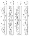
- FIGS. 3 a - 3 dillustrate a method of manufacturing semiconductor device 100 having an interconnect structure providing top and bottom interconnects formed by solder bumps.
- substrate 102is provided.
- substrate 102includes a bare Cu sheet suitable for attaching a plurality of solder bumps.
- substrate 102includes other metals or substrate materials over which solder bumps may be deposited and connected.
- a solder materialis deposited over substrate 102 using a ball drop or stencil printing process, for example.
- the solder materialincludes an electrically conductive material such as Sn, Pb, Au, Ag, Cu, Zn, Bi, and alloys thereof, with an optional flux material.
- the solder materialcan be eutectic Sn/Pb, high lead, or lead free.
- the solder (or other conductive material)is reflowed to form bumps 104 .
- Bumps 104are mechanically connected to substrate 102 .
- Die 106is mounted to substrate 102 using die attach adhesive 110 .
- Die 106includes semiconductor devices, or other electronic chips or ICs and provides various functions such as memory, controller, ASICs, processor, microcontroller, or combinations thereof.
- Die attach adhesive 110includes an underfill or epoxy polymer material for bonding die 106 to substrate 102 .
- die attach adhesive 110includes a laminated polymer adhesive or an ultra-violet (UV) curable liquid adhesive, for example.
- Contact pads 108are made with a conductive material, such as Al, Cu, Sn, Ni, Au, or Ag, and are electrically connected to the circuit elements formed within die 106 . Contact pads 108 are formed by PVD, CVD, electrolytic plating, or electroless plating processes, for example.
- encapsulant 112is deposited over substrate 102 around bumps 104 and over die 106 .
- Encapsulant 112includes an epoxy resin, or polyimide, for example, and may be deposited by spin-coating, dispensing, or printing.
- the deposition of encapsulant 112is controlled to expose a top surface of bumps 104 .
- 1-25% of the surface of bumps 104are exposed above the encapsulant 112 .
- the exposed portions of bumps 104are flattened after deposition of encapsulant 112 to be level with a top surface of encapsulant 112 .
- Vias 114are formed in encapsulant 112 by blind etching to expose contact pads 108 .
- Blind etchinginvolves removing a portion of encapsulant 112 and may be performed by laser drilling or etching, wet etching, or another etching process.
- redistribution layer (RDL) 116is deposited over semiconductor device 100 to interconnect bumps 104 and contact pads 108 of die 106 .
- RDL 116can be made with Ni, NiV, Cu, or other conductive materials.
- RDL 116routes electrical signals between die 106 and bumps 104 .
- RDL 116is formed by PVD, CVD, electrolytic plating, or electroless plating processes. With RDL 116 deposited, bumps 104 are electrically connected to the circuits and devices formed within die 106 .
- a backgrinding processis applied to substrate 102 to remove substrate 102 and to expose a back surface of bumps 104 and die attach adhesive 110 .
- the backgrinding processmay involve chemical-mechanical polishing (CMP), wet etching, plasma etching, or another etching process suitable for removing substrate 102 .
- CMPchemical-mechanical polishing
- semiconductor device 100may be mounted to motherboards, PCBs, or other substrates using bumps 104 as the interconnect structure for placing die 106 in communication with other system components.
- An optional passivation layer(not shown) is deposited over semiconductor device 100 to cover RDL 116 and provide electrical insulation and physical protection.
- the optional passivation layermay include one or more layers of silicon dioxide (SiO2), silicon nitride (Si3N4), silicon oxy-nitride (SiON), or another insulating material.
- a semiconductor deviceis formed that provides a wafer-level chip-scale package (WLCSP) having both top and bottom surface interconnects.
- WLCSPwafer-level chip-scale package
- the interconnect structureis formed by a plurality of solder bumps.
- the bumpsare formed using a simplified manufacturing process that allows for formation of the bumps directly over a copper strip, or other metal substrate. Because the bumps are formed directly on the substrate, additional pad layers for building up the bumps or insulation layers are not necessary.
- An encapsulantis deposited over the device and a top and bottom surface of the solder bumps are exposed to provide top and bottom surface interconnects for the semiconductor device.
- An RDL structureis formed over the device to interconnect the bumps and the die.
- the RDL structureis flat and formed directly over a surface of the encapsulant. Because the interconnect structure of the semiconductor device is formed by solder bumps rather than small input/output pins, the process of mounting the device to a motherboard configured for BGA-type device mounting is simplified. Accordingly, the present method mitigates several difficulties associated with forming WLCSPs using dies having relatively high input/output pin counts.
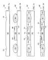
- FIGS. 4 a and 4 billustrate alternative configurations for the plurality of solder bumps that form the interconnect structure of the present semiconductor device.
- a plurality of solder bumps 206are disposed within encapsulant 202 deposited around die 200 .
- the deposition of encapsulant 202is controlled to expose a top surface of bumps 206 and contact pads 204 that are formed over a surface of die 200 .
- RDL 208is formed over a surface of encapsulant 202 and die 200 to form an electrical interconnection between die 200 and bumps 206 .
- bumps 206provide a single row of interconnect structures to facilitate mounting the device to other system components.
- bumps 206are configured in multiple rows. As shown in FIG. 4 b, bumps 206 are configured in two rows of staggered bumps 206 .
- RDL 208is deposited over die 200 and encapsulant 202 to connect bumps 206 from both rows to contact pads 204 of die 200 .
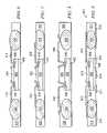
- FIGS. 5 a - 5 dillustrate a method of manufacturing semiconductor device 300 having an interconnect structure providing top and bottom interconnects formed by solder bumps, semiconductor device 300 is manufactured using a substrate having solder capture dents 301 .
- substrate 302is provided.
- substrate 302includes a bare Cu sheet suitable for attaching a plurality of solder bumps.
- Solder capture dents 301are formed within a surface of substrate 302 to facilitate the deposition of conductive material over susbtrate 302 .
- solder capture dents 301are configured to receive 1-25% of the total volume of bumps 304 .
- the geometric shape of solder capture dents 301is semi-spherical, however other configurations may be used depending upon the application.
- solder materialis deposited over solder capture dents 301 of substrate 302 using a ball drop or stencil printing process, for example.
- the solder materialincludes an electrically conductive material such as Sn, Pb, Au, Ag, Cu, Zn, Bi, and alloys thereof, with an optional flux material.
- the solder (or other conductive material)is reflowed to form bumps 304 .
- Bumps 304are mechanically connected to substrate 302 .
- Die 306is mounted to substrate 302 using die attach adhesive 310 .
- Die 306includes semiconductor devices, or other electronic chips or ICs and provides various functions such as memory, controller, ASICs, processor, microcontroller, or combinations thereof.
- Die attach adhesive 310includes an underfill or epoxy polymer material for bonding die 306 to substrate 302 .
- die attach adhesive 310includes a laminated polymer adhesive or an UV curable liquid adhesive, for example.
- Contact pads 308are made with a conductive material, such as Al, Cu, Sn, Ni, Au, or Ag, and are electrically connected to the circuit elements formed within die 306 . Contact pads 308 are formed by PVD, CVD, electrolytic plating, or electroless plating processes, for example.
- encapsulant 312is deposited over substrate 302 around bumps 304 and over die 306 .
- Encapsulant 312includes an epoxy resin, or polyimide, for example, and may be deposited by spin-coating, dispensing, printing, or transfer molding. As shown in FIG. 5 c, the deposition of encapsulant 312 is controlled to expose a top surface of bumps 304 , or encapsulant 312 may be planarized to expose bumps 304 .
- Vias 314are formed in encapsulant 312 by blind etching to expose contact pads 308 . Blind etching involves removing a portion of encapsulant 312 and may be performed by laser drilling or etching, wet etching, or another etching process.
- RDL 316is deposited over semiconductor device 300 to interconnect bumps 304 and contact pads 308 of die 306 .
- RDL 316can be made with Ni, NiV, Cu, or other conductive materials.
- RDL 316routes electrical signals between die 306 and bumps 304 .
- RDL 316is formed by PVD, CVD, electrolytic plating, or electroless plating processes. With RDL 316 deposited, bumps 304 are electrically connected to the circuits and devices formed within die 306 .
- a backgrinding processis applied to substrate 302 to remove substrate 302 and to expose a back surface of bumps 304 and die attach adhesive 310 .
- the backgrinding processmay involve CMP, wet etching, plasma etching, or another etching process suitable for removing substrate 302 .
- semiconductor device 300With substrate 302 removed, semiconductor device 300 may be mounted to motherboards, PCBs, or other substrates using bumps 304 as the interconnect structure for placing die 306 in communication with other system components.
- An optional passivation layer(not shown) is deposited over semiconductor device 300 to cover RDL 316 and provide electrical insulation and physical protection.
- the optional passivation layermay include one or more layers of SiO2, Si3N4, SiON, or another insulating material.
- FIG. 6illustrates a semiconductor device having an interconnect structure providing top and bottom interconnects formed by solder bumps, a top surface of the solder bumps protrudes past a top-surface of the encapsulant.
- Solder bumps 402are formed using a ball drop or stencil printing process. Solder material is reflowed to form solder bumps 402 .
- Die 404is mounted next to bumps 402 using die attach adhesive 408 .
- Die 404includes semiconductor devices, or other electronic chips or ICs and provides various functions such as memory, controller, ASICs, processor, microcontroller, or combinations thereof.
- Die attach adhesive 408includes an underfill or epoxy polymer material.
- Contact pads 406are made with a conductive material, such as Al, Cu, Sn, Ni, Au, or Ag, and are electrically connected to the circuit elements formed within die 404 .
- Contact pads 406are formed by PVD, CVD, electrolytic plating, or electroless plating processes, for example.
- Encapsulant 410is deposited around bumps 402 and over die 404 .
- Encapsulant 410includes an epoxy resin, or polyimide, for example, and may be deposited by spin-coating, dispensing, or printing. As shown in FIG. 6 , the deposition of encapsulant 410 is controlled to expose a top surface of bumps 402 . Vias are formed in encapsulant 410 by blind etching to expose contact pads 408 .
- RDL 412is deposited over encapsulant 410 to interconnect bumps 402 and contact pads 406 of die 404 .
- RDL 412can be made with Ni, NiV, Cu, or other conductive materials.
- RDL 412routes electrical signals between die 404 and bumps 402 .
- RDL 412is formed by PVD, CVD, electrolytic plating, or electroless plating processes. With RDL 412 deposited, bumps 402 are electrically connected to the circuits and devices formed within die 404 .
- An optional passivation layer(not shown) is deposited over the semiconductor device to cover RDL 412 and provide electrical insulation and physical protection.
- the optional passivation layermay include one or more layers of SiO2, Si3N4, SiON, or another insulating material.
- FIG. 7illustrates a semiconductor device having an interconnect structure providing top and bottom interconnects formed by solder bumps, a top surface of the semiconductor device is planarized to expose the solder bumps.
- Solder bumps 414are formed using a ball drop or stencil printing process. Solder material is reflowed to form solder bumps 414 .
- Die 416is mounted next to bumps 414 using die attach adhesive 420 .
- Die 416includes semiconductor devices, or other electronic chips or ICs and provides various functions such as memory, controller, ASICs, processor, microcontroller, or combinations thereof.
- Die attach adhesive 420includes an underfill or epoxy polymer material.
- Contact pads 418are made with a conductive material, such as Al, Cu, Sn, Ni, Au, or Ag, and are electrically connected to the circuit elements formed within die 416 .
- Contact pads 418are formed by PVD, CVD, electrolytic plating, or electroless plating processes, for example.
- Encapsulant 422is deposited over bumps 414 and over die 416 .
- Encapsulant 422includes an epoxy resin, or polyimide, for example, and may be deposited by spin-coating, dispensing, or printing. After encapsulant 422 is deposited, it is planarized to remove a portion of encapsulant 422 and to expose a top surface of bumps 414 . During planarization, a portion of both encapsulant 422 and bumps 424 may be removed.
- Encapsulant 422is planarized using a CMP, mechanical backgrinding, plasma etching, wet etch, dry etch or other thinning or planarization process. Vias are formed in encapsulant 422 by blind etching to expose contact pads 418 .
- RDL 424is deposited over encapsulant 422 to interconnect bumps 414 and contact pads 418 of die 416 .
- RDL 424can be made with Ni, NiV, Cu, or other conductive materials.
- RDL 424routes electrical signals between die 416 and bumps 414 .
- RDL 424is formed by PVD, CVD, electrolytic plating, or electroless plating processes. With RDL 424 deposited, bumps 414 are electrically connected to the circuits and devices formed within die 416 .
- An optional passivation layer(not shown) is deposited over the semiconductor device to cover RDL 424 and provide electrical insulation and physical protection.
- the optional passivation layermay include one or more layers of SiO2, Si3N4, SiON, or another insulating material.
- FIG. 8illustrates a semiconductor device having an interconnect structure providing top and bottom interconnects formed by solder bumps, vias are formed in the encapsulant to expose contact pads of the die and a top surface of the solder bumps.
- Solder bumps 426are formed using a ball drop or stencil printing process. Solder material is reflowed to form solder bumps 426 .
- Die 428is mounted next to bumps 426 using die attach adhesive 432 .
- Die 428includes semiconductor devices, or other electronic chips or ICs and provides various functions such as memory, controller, ASICs, processor, microcontroller, or combinations thereof.
- Die attach adhesive 432includes an underfill or epoxy polymer material.
- Contact pads 430are made with a conductive material, such as Al, Cu, Sn, Ni, Au, or Ag, and are electrically connected to the circuit elements formed within die 428 .
- Contact pads 430are formed by PVD, CVD, electrolytic plating, or electroless plating processes, for example.
- Encapsulant 434is deposited over bumps 426 and over die 428 .
- Encapsulant 434includes an epoxy resin, or polyimide, for example, and may be deposited by spin-coating, dispensing, or printing. Vias are formed in encapsulant 434 by blind etching to expose both contact pads 430 and a top surface of bumps 426 .
- RDL 436is deposited over encapsulant 434 to interconnect bumps 426 and contact pads 430 of die 428 .
- RDL 436can be made with Ni, NiV, Cu, or other conductive materials.
- RDL 436routes electrical signals between die 428 and bumps 426 .
- RDL 436is formed by PVD, CVD, electrolytic plating, or electroless plating processes.
- RDL 436is deposited conformally over a surface of encapsulant 434 into the vias formed over contact pads 430 of die 428 and bumps 426 . With RDL 436 deposited, bumps 426 are electrically connected to the circuits and devices formed within die 428 .
- An optional passivation layer(not shown) is deposited over the semiconductor device to cover RDL 436 and provide electrical insulation and physical protection.
- the optional passivation layermay include one or more layers of SiO2, Si3N4, SiON, or another insulating material.
- FIG. 9illustrates semiconductor device 500 having an interconnect structure providing top and bottom interconnects formed by solder bumps, RDLs are formed over a top surface and a bottom surface of semiconductor device 500 .
- Solder bumps 502are formed using a ball drop or stencil printing process. Solder material is reflowed to form solder bumps 502 .
- Die 504is mounted next to bumps 502 using die attach adhesive 508 .
- Die 504includes semiconductor devices, or other electronic chips or ICs and provides various functions such as memory, controller, ASICs, processor, microcontroller, or combinations thereof.
- Die attach adhesive 508includes an underfill or epoxy polymer material.
- Contact pads 506are made with a conductive material, such as Al, Cu, Sn, Ni, Au, or Ag, and are electrically connected to the circuit elements formed within die 504 .
- Contact pads 506are formed by PVD, CVD, electrolytic plating, or electroless plating processes, for example.
- Encapsulant 510is deposited around bumps 502 and over die 504 .
- Encapsulant 510includes an epoxy resin, or polyimide, for example, and may be deposited by spin-coating, dispensing, or printing. As shown in FIG. 9 , the deposition of encapsulant 510 is controlled to expose a top surface of bumps 502 . Vias are formed in encapsulant 510 by blind etching to expose contact pads 506 .
- RDL 512is deposited over encapsulant 510 to interconnect bumps 502 and contact pads 506 of die 504 .
- RDL 512can be made with Ni, NiV, Cu, or other conductive materials.
- RDL 512routes electrical signals between die 504 and bumps 502 .
- RDL 512is formed by PVD, CVD, electrolytic plating, or electroless plating processes. With RDL 512 deposited, bumps 502 are electrically connected to the circuits and devices formed within die 504 . As shown in FIG. 9 , RDL 514 is formed over a back surface of semiconductor device 500 .
- RDL 514may form electrical connections between one or more bumps 502 and contact pads 506 of die 504 , or may provide an alternative electrical interconnection network for connecting semiconductor device 500 to other system components.
- additional layers of under-bump metallization or polyimide layersare formed over the device to provide additional routing capability and top and bottom interconnect pad formations.
- RDLs 512 and 514may be used for re-routing electrical signals and the creation of pads and/or interconnect bumps for mounting semiconductor device 500 to a PCB or for device stacking.
- An optional passivation layer(not shown) is deposited over the semiconductor device to cover RDLs 512 and 514 and provide electrical insulation and physical protection.
- the optional passivation layermay include one or more layers of SiO2, Si3N4, SiON, or another insulating material.
Landscapes
- Engineering & Computer Science (AREA)
- Microelectronics & Electronic Packaging (AREA)
- Power Engineering (AREA)
- Computer Hardware Design (AREA)
- Physics & Mathematics (AREA)
- Condensed Matter Physics & Semiconductors (AREA)
- General Physics & Mathematics (AREA)
- Manufacturing & Machinery (AREA)
- Internal Circuitry In Semiconductor Integrated Circuit Devices (AREA)
- Structures Or Materials For Encapsulating Or Coating Semiconductor Devices Or Solid State Devices (AREA)
Abstract
Description
- The present invention relates in general to semiconductor devices and, more particularly, to a semiconductor device including a wafer-level chip-scale package (CSP) having a solder bump top and bottom interconnect structure.
- Semiconductor devices are commonly found in modern electronic products. Semiconductor devices vary in the number and density of electrical components. Discrete semiconductor devices generally contain one type of electrical component, e.g., light emitting diode (LED), transistor, resistor, capacitor, inductor, and power metal oxide semiconductor field effect transistor (MOSFET). Integrated semiconductor devices typically contain hundreds to millions of electrical components. Examples of integrated semiconductor devices include microcontrollers, microprocessors, charged-coupled devices (CCDs), solar cells, and digital micro-mirror devices (DMDs).
- Semiconductor devices perform a wide range of functions such as high-speed calculations, transmitting and receiving electromagnetic signals, controlling electronic devices, transforming sunlight to electricity, and creating visual projections for television displays. Semiconductor devices are found in the fields of entertainment, communications, power generation, networks, computers, and consumer products. Semiconductor devices are also found in electronic products including military, aviation, automotive, industrial controllers, and office equipment.
- Semiconductor devices exploit the electrical properties of semiconductor materials. The atomic structure of semiconductor material allows its electrical conductivity to be manipulated by the application of an electric field or through the process of doping. Doping introduces impurities into the semiconductor material.
- A semiconductor device contains active and passive electrical structures. Active structures, including transistors, control the flow of electrical current. By varying levels of doping and application of an electric field, the transistor either promotes or restricts the flow of electrical current. Passive structures, including resistors, diodes, and inductors, create a relationship between voltage and current necessary to perform a variety of electrical functions. The passive and active structures are electrically connected to form logic circuits, which enable the semiconductor device to perform high-speed calculations and other useful functions.
- Semiconductor devices are generally manufactured using two complex manufacturing processes, i.e., front-end manufacturing, and back-end manufacturing, each involving potentially hundreds of steps. Front-end manufacturing involves the formation of a plurality of die on the surface of a semiconductor wafer. Each die is typically identical and contains circuits formed by electrically connecting active and passive components. Back-end manufacturing involves singulating individual die from the finished wafer and packaging the die to provide structural support and environmental isolation.
- One goal of semiconductor manufacturing is to produce smaller semiconductor devices. Smaller devices typically consume less power, have higher performance, and can be produced more efficiently. In addition, smaller semiconductor devices have a smaller footprint, which is desirable for smaller end products. A smaller die size may be achieved by improvements in the front-end process resulting in die with smaller, higher density active and passive components. Back-end processes may result in semiconductor device packages with a smaller footprint by improvements in electrical interconnection and packaging materials.
- Often, when forming wafer-level chip-scale packages (WLCSPs), it is necessary to form top and bottom interconnection structures in the packages. The top and bottom interconnect structure facilitates the mounting of the WLCSPs to motherboards, and other printed circuit boards (PCBs) or substrates. Furthermore, by forming the interconnections on top and bottom surfaces of the package, multiple WLCSPs can be placed over one-another to form stacked packages that provide sophisticated functionality in a small package volume. The top and bottom interconnects usually include conductive through-hole vias (THVs) formed within a perimeter of the WLCSP. Conductive THVs are difficult to manufacture and require several additional fabrication steps that increase the cost and manufacturing time of the WLCSP. Furthermore, as fabrication technologies improve, average die size shrinks and the number of input/output pins per die increases. Due to the increasing pin density, it is difficult to mount the resulting die to conventional motherboards which are configured for ball grid array (BGA) mounting technologies using larger input/output bumps with a larger pitch.
- In one embodiment, the present invention is a method of making a semiconductor device comprising the steps of providing a metal substrate for supporting the semiconductor device, connecting solder bumps to the substrate, and mounting a semiconductor die to the substrate using a die attach adhesive. The semiconductor die has a plurality of contact pads formed over a surface of the semiconductor die. The method includes depositing encapsulant over the solder bumps and the semiconductor die, etching the encapsulant to expose the contact pads of the semiconductor die, and forming a first redistribution layer (RDL) over the encapsulant to connect each contact pad of the semiconductor die to one of the solder bumps. The method includes removing the substrate to expose the die attach adhesive and a bottom surface of the solder bumps.
- In another embodiment, the present invention is a method of making a semiconductor device comprising the steps of providing a substrate for supporting the semiconductor device, connecting a solder bump to the substrate, and mounting a semiconductor die to the substrate. The semiconductor die has a contact pad formed over a surface of the semiconductor die. The method includes depositing encapsulant over the solder bump and the semiconductor die, etching the encapsulant to expose the contact pads of the semiconductor die, and forming a first redistribution layer (RDL) over the encapsulant to connect the contact pad of the semiconductor die to the solder bump. The method includes removing the substrate to expose a bottom surface of the solder bump.
- In another embodiment, the present invention is a method of making a semiconductor device comprising the steps of providing a substrate for supporting the semiconductor device, connecting a conductive bump to the substrate, mounting a semiconductor die to the substrate, and depositing encapsulant over the conductive bump and the semiconductor die. The method includes forming a redistribution layer (RDL) over the encapsulant to connect the semiconductor die to the conductive bump, and removing the substrate to expose a bottom surface of the conductive bump.
- In another embodiment, the present invention is a semiconductor device comprising a semiconductor die having a plurality of contact pads formed over a surface of the semiconductor die, a plurality of solder bumps disposed around a perimeter of the semiconductor die, and an encapsulant material formed around the solder bumps and over the semiconductor die. The encapsulant exposes a top portion and a bottom portion of each solder bump. The device includes a plurality of vias etched into the encapsulant to expose the contact pads of the semiconductor die, and a first redistribution layer (RDL) formed over the encapsulant to connect each contact pad of the semiconductor die to one of the solder bumps.
FIG. 1 illustrates a printed circuit board (PCB) with different types of packages mounted to its surface;FIGS. 2 a-2cillustrate further detail of the representative semiconductor packages mounted to the PCB;FIGS. 3 a-3dillustrate a method of manufacturing a semiconductor device having an interconnect structure providing top and bottom interconnects formed by solder bumps;FIGS. 4 aand4billustrate alternative configurations for the plurality of solder bumps that form the interconnect structure of the present semiconductor device;FIGS. 5 a-5dillustrate a method of manufacturing a semiconductor device having an interconnect structure providing top and bottom interconnects formed by solder bumps, the semiconductor device is manufactured using a substrate having solder capture dents;FIG. 6 illustrates a semiconductor device having an interconnect structure providing top and bottom interconnects formed by solder bumps, a top surface of the solder bumps protrudes past a top-surface of the encapsulant;FIG. 7 illustrates a semiconductor device having an interconnect structure providing top and bottom interconnects formed by solder bumps, a top surface of the semiconductor device is planarized to expose the solder bumps;FIG. 8 illustrates a semiconductor device having an interconnect structure providing top and bottom interconnects formed by solder bumps, vias are formed in the encapsulant to expose contact pads of the die and a top surface of the solder bumps; andFIG. 9 illustrates a semiconductor device having an interconnect structure providing top and bottom interconnects formed by solder bumps, redistribution layers (RDLs) are formed over a top surface and a bottom surface of the semiconductor device.- The present invention is described in one or more embodiments in the following description with reference to the Figures, in which like numerals represent the same or similar elements. While the invention is described in terms of the best mode for achieving the invention's objectives, it will be appreciated by those skilled in the art that it is intended to cover alternatives, modifications, and equivalents as may be included within the spirit and scope of the invention as defined by the appended claims and their equivalents as supported by the following disclosure and drawings.
- Semiconductor devices are generally manufactured using two complex manufacturing processes: front-end manufacturing and back-end manufacturing. Front-end manufacturing involves the formation of a plurality of die on the surface of a semiconductor wafer. Each die on the wafer contains active and passive electrical components which are electrically connected to form functional electrical circuits. Active electrical components, such as transistors, have the ability to control the flow of electrical current. Passive electrical components, such as capacitors, inductors, resistors, and transformers, create a relationship between voltage and current necessary to perform electrical circuit functions.
- Passive and active components are formed on the surface of the semiconductor wafer by a series of process steps including doping, deposition, photolithography, etching, and planarization. Doping introduces impurities into the semiconductor material by techniques such as ion implantation or thermal diffusion. The doping process modifies the electrical conductivity of semiconductor material in active devices, transforming the semiconductor material into a permanent insulator, permanent conductor, or changing the way the semiconductor material changes in conductivity in response to an electric field. Transistors contain regions of varying types and degrees of doping arranged as necessary to enable the transistor to promote or restrict the flow of electrical current upon the application of an electric field.
- Active and passive components are formed by layers of materials with different electrical properties. The layers can be formed by a variety of deposition techniques determined in part by the type of material being deposited. For example, thin film deposition may involve chemical vapor deposition (CVD), physical vapor deposition (PVD), electrolytic plating, and electroless plating processes. Each layer is generally patterned to form portions of active components, passive components, or electrical connections between components.
- The layers can be patterned using photolithography, which involves the deposition of light sensitive material, e.g., photoresist, over the layer to be patterned. A pattern is transferred from a photomask to the photoresist using light. The portion of the photoresist pattern subjected to light is removed using a solvent, exposing portions of the underlying layer to be patterned. The remainder of the photoresist is removed, leaving behind a patterned layer. Alternatively, some types of materials are patterned by directly depositing the material into the areas or voids formed by a previous deposition/etch process using techniques such as electrolytic plating.
- Depositing a thin film of material over an existing pattern can exaggerate the underlying pattern and create a non-uniformly flat surface. A uniformly flat surface is required to produce smaller and more densely packed active and passive components. Planarization can be used to remove material from the surface of the wafer and produce a uniformly flat surface. Planarization involves polishing the surface of the wafer with a polishing pad. An abrasive material and corrosive chemical are added to the surface of the wafer during polishing. The combined mechanical action of the abrasive and corrosive action of the chemical removes any irregular topography, resulting in a uniformly flat surface.
- Back-end manufacturing refers to cutting or singulating the finished wafer into the individual die and then packaging the die for structural support and environmental isolation. To singulate the die, the wafer is scored and broken along non-functional regions of the wafer called saw streets or scribes. The wafer is singulated using a laser cutting device or saw blade. After singulation, the individual die are mounted to a package substrate that includes pins or contact pads for interconnection with other system components. Contact pads formed over the semiconductor die are then connected to contact pads within the package. The electrical connections can be made with solder bumps, stud bumps, conductive paste, or wirebonds. An encapsulant or other molding material is deposited over the package to provide physical support and electrical isolation. The finished package is then inserted into an electrical system and the functionality of the semiconductor device is made available to the other system components.
FIG. 1 illustrateselectronic device 10 having a chip carrier substrate or printed circuit board (PCB)12 with a plurality of semiconductor packages mounted on its surface.Electronic device 10 may have one type of semiconductor package, or multiple types of semiconductor packages, depending on the application. The different types of semiconductor packages are shown inFIG. 1 for purposes of illustration.Electronic device 10 may be a stand-alone system that uses the semiconductor packages to perform an electrical function. Alternatively,electronic device 10 may be a subcomponent of a larger system. For example,electronic device 10 may be a graphics card, network interface card, or other signal processing card that can be inserted into a computer. The semiconductor package can include microprocessors, memories, application specific integrated circuits (ASICs), logic circuits, analog circuits, RF circuits, discrete devices, or other semiconductor die or electrical components.- In
FIG. 1 ,PCB 12 provides a general substrate for structural support and electrical interconnect of the semiconductor packages mounted on the PCB. Conductive signal traces14 are formed on a surface or within layers ofPCB 12 using evaporation, electrolytic plating, electroless plating, screen printing, PVD, or other suitable metal deposition process. Signal traces14 provide for electrical communication between each of the semiconductor packages, mounted components, and other external system components.Traces 14 also provide power and ground connections to each of the semiconductor packages. - In some embodiments, a semiconductor device has two packaging levels. First level packaging is the technique for mechanically and electrically attaching the semiconductor die to a carrier. Second level packaging involves mechanically and electrically attaching the carrier to the PCB. In other embodiments, a semiconductor device may only have the first level packaging where the die is mechanically and electrically mounted directly to the PCB.
- For the purpose of illustration, several types of first level packaging, including
wire bond package 16 andflip chip 18, are shown onPCB 12. Additionally, several types of second level packaging, including ball grid array (BGA)20, bump chip carrier (BCC)22, dual in-line package (DIP)24, land grid array (LGA)26, multi-chip module (MCM)28, quad flat non-leaded package (QFN)30, and quadflat package 32, are shown mounted onPCB 12. Depending upon the system requirements, any combination of semiconductor packages, configured with any combination of first and second level packaging styles, as well as other electronic components, can be connected toPCB 12. In some embodiments,electronic device 10 includes a single attached semiconductor package, while other embodiments call for multiple interconnected packages. By combining one or more semiconductor packages over a single substrate, manufacturers can incorporate pre-made components into electronic devices and systems. Because the semiconductor packages include sophisticated functionality, electronic devices can be manufactured using cheaper components and a shorter manufacturing process. The resulting devices are less likely to fail and less expensive to manufacture resulting in lower costs for consumers. FIG. 2 aillustrates further detail ofDIP 24 mounted onPCB 12.DIP 24 includes semiconductor die34 havingcontact pads 36. Semiconductor die34 includes an active area containing analog or digital circuits implemented as active devices, passive devices, conductive layers, and dielectric layers formed within semiconductor die34 and are electrically interconnected according to the electrical design of the die. For example, the circuit may include one or more transistors, diodes, inductors, capacitors, resistors, and other circuit elements formed within the active area ofdie 34. Contactpads 36 are made with a conductive material, such as aluminum (Al), copper (Cu), tin (Sn), nickel (Ni), gold (Au), or silver (Ag), and are electrically connected to the circuit elements formed withindie 34. Contactpads 36 are formed by PVD, CVD, electrolytic plating, or electroless plating process. During assembly ofDIP 24, semiconductor die34 is mounted to acarrier 38 using a gold-silicon eutectic layer or adhesive material such as thermal epoxy. The package body includes an insulative packaging material such as plastic or ceramic. Conductor leads40 are connected tocarrier 38 andwire bonds 42 are formed betweenleads 40 andcontact pads 36 ofdie 34 as a first level packaging.Encapsulant 44 is deposited over the package for environmental protection by preventing moisture and particles from entering the package and contaminatingdie 34,contact pads 36, or wire bonds42.DIP 24 is connected toPCB 12 by insertingleads 40 into holes formed throughPCB 12.Solder material 46 is flowed around leads40 and into the holes to physically and electrically connectDIP 24 toPCB 12.Solder material 46 can be any metal or electrically conductive material, e.g., Sn, lead (Pb), Au, Ag, Cu, zinc (Zn), bismuthinite (Bi), and alloys thereof, with an optional flux material. For example, the solder material can be eutectic Sn/Pb, high-lead, or lead-free.FIG. 2 billustrates further detail ofBCC 22 mounted onPCB 12. Semiconductor die16 is connected to a carrier by wire bond style first level packaging.BCC 22 is mounted toPCB 12 with a BCC style second level packaging. Semiconductor die16 havingcontact pads 48 is mounted over a carrier using an underfill or epoxy-resin adhesive material 50. Semiconductor die16 includes an active area containing analog or digital circuits implemented as active devices, passive devices, conductive layers, and dielectric layers formed within semiconductor die16 and are electrically interconnected according to the electrical design of the die. For example, the circuit may include one or more transistors, diodes, inductors, capacitors, resistors, and other circuit elements formed within the active area ofdie 16. Contactpads 48 are made with a conductive material, such as Al, Cu, Sn, Ni, Au, or Ag, and are electrically connected to the circuit elements formed withindie 16. Contactpads 48 are formed by PVD, CVD, electrolytic plating, or electroless plating process.Wire bonds 54 andbond pads contact pads 48 of semiconductor die16 to contactpads 52 ofBCC 22 forming the first level packaging. Molding compound orencapsulant 60 is deposited over semiconductor die16,wire bonds 54,contact pads 48, andcontact pads 52 to provide physical support and electrical isolation for the device. Contactpads 64 are formed on a surface ofPCB 12 using evaporation, electrolytic plating, electroless plating, screen printing, PVD, or other suitable metal deposition process and are typically plated to prevent oxidation. Contactpads 64 electrically connect to one or more conductive signal traces14. Solder material is deposited betweencontact pads 52 ofBCC 22 andcontact pads 64 ofPCB 12. The solder material is reflowed to formbumps 66 which form a mechanical and electrical connection betweenBCC 22 andPCB 12.- In
FIG. 2 c,semiconductor die18 is mounted face down tocarrier 76 with a flip chip style first level packaging.BGA 20 is attached toPCB 12 with a BGA style second level packaging.Active area 70 containing analog or digital circuits implemented as active devices, passive devices, conductive layers, and dielectric layers formed within semiconductor die18 is electrically interconnected according to the electrical design of the die. For example, the circuit may include one or more transistors, diodes, inductors, capacitors, resistors, and other circuit elements formed withinactive area 70 of semiconductor die18. Semiconductor die18 is electrically and mechanically attached to thecarrier 76 through a large number of individual conductive solder bumps orballs 78. Solder bumps78 are formed on bump pads orinterconnect sites 80, which are disposed onactive areas 70.Bump pads 80 are made with a conductive material, such as Al, Cu, Sn, Ni, Au, or Ag, and are electrically connected to the circuit elements formed inactive area 70.Bump pads 80 are formed by PVD, CVD, electrolytic plating, or electroless plating process. Solder bumps78 are electrically and mechanically connected to contact pads orinterconnect sites 82 oncarrier 76 by a solder reflow process. BGA 20 is electrically and mechanically attached toPCB 12 by a large number of individual conductive solder bumps orballs 86. The solder bumps are formed on bump pads orinterconnect sites 84. Thebump pads 84 are electrically connected to interconnectsites 82 throughconductive lines 90 routed throughcarrier 76. Contactpads 88 are formed on a surface ofPCB 12 using evaporation, electrolytic plating, electroless plating, screen printing, PVD, or other suitable metal deposition process and are typically plated to prevent oxidation. Contactpads 88 electrically connect to one or more conductive signal traces14. The solder bumps86 are electrically and mechanically connected to contact pads orbonding pads 88 onPCB 12 by a solder reflow process. Molding compound orencapsulant 92 is deposited over semiconductor die18 andcarrier 76 to provide physical support and electrical isolation for the device. The flip chip semiconductor device provides a short electrical conduction path from the active devices on semiconductor die18 to conduction tracks onPCB 12 in order to reduce signal propagation distance, lower capacitance, and achieve overall better circuit performance. In another embodiment, the semiconductor die18 can be mechanically and electrically attached directly toPCB 12 using flip chip style first level packaging withoutcarrier 76.FIGS. 3 a-3dillustrate a method ofmanufacturing semiconductor device 100 having an interconnect structure providing top and bottom interconnects formed by solder bumps. Turning toFIG. 3 a,substrate 102 is provided. In one embodiment,substrate 102 includes a bare Cu sheet suitable for attaching a plurality of solder bumps. In alternative embodiments,substrate 102 includes other metals or substrate materials over which solder bumps may be deposited and connected. A solder material is deposited oversubstrate 102 using a ball drop or stencil printing process, for example. The solder material includes an electrically conductive material such as Sn, Pb, Au, Ag, Cu, Zn, Bi, and alloys thereof, with an optional flux material. For example, the solder material can be eutectic Sn/Pb, high lead, or lead free. The solder (or other conductive material) is reflowed to form bumps104.Bumps 104 are mechanically connected tosubstrate 102.Die 106 is mounted tosubstrate 102 using die attach adhesive110.Die 106 includes semiconductor devices, or other electronic chips or ICs and provides various functions such as memory, controller, ASICs, processor, microcontroller, or combinations thereof. Die attach adhesive110 includes an underfill or epoxy polymer material for bonding die106 tosubstrate 102. In alternative embodiments, die attach adhesive110 includes a laminated polymer adhesive or an ultra-violet (UV) curable liquid adhesive, for example. Contactpads 108 are made with a conductive material, such as Al, Cu, Sn, Ni, Au, or Ag, and are electrically connected to the circuit elements formed withindie 106. Contactpads 108 are formed by PVD, CVD, electrolytic plating, or electroless plating processes, for example.- Turning to
FIG. 3 b,encapsulant 112 is deposited oversubstrate 102 aroundbumps 104 and over die106.Encapsulant 112 includes an epoxy resin, or polyimide, for example, and may be deposited by spin-coating, dispensing, or printing. As shown inFIG. 3 b,the deposition ofencapsulant 112 is controlled to expose a top surface ofbumps 104. Depending upon the application, 1-25% of the surface ofbumps 104 are exposed above theencapsulant 112. In an alternative embodiment, the exposed portions ofbumps 104 are flattened after deposition ofencapsulant 112 to be level with a top surface ofencapsulant 112.Vias 114 are formed inencapsulant 112 by blind etching to exposecontact pads 108. Blind etching involves removing a portion ofencapsulant 112 and may be performed by laser drilling or etching, wet etching, or another etching process. - Turning to
FIG. 3 c,redistribution layer (RDL)116 is deposited oversemiconductor device 100 to interconnectbumps 104 andcontact pads 108 ofdie 106.RDL 116 can be made with Ni, NiV, Cu, or other conductive materials.RDL 116 routes electrical signals betweendie 106 and bumps104.RDL 116 is formed by PVD, CVD, electrolytic plating, or electroless plating processes. WithRDL 116 deposited, bumps104 are electrically connected to the circuits and devices formed withindie 106. - Turning to
FIG. 3 d,a backgrinding process is applied tosubstrate 102 to removesubstrate 102 and to expose a back surface ofbumps 104 and die attach adhesive110. The backgrinding process may involve chemical-mechanical polishing (CMP), wet etching, plasma etching, or another etching process suitable for removingsubstrate 102. Withsubstrate 102 removed,semiconductor device 100 may be mounted to motherboards, PCBs, or othersubstrates using bumps 104 as the interconnect structure for placingdie 106 in communication with other system components. An optional passivation layer (not shown) is deposited oversemiconductor device 100 to coverRDL 116 and provide electrical insulation and physical protection. The optional passivation layer may include one or more layers of silicon dioxide (SiO2), silicon nitride (Si3N4), silicon oxy-nitride (SiON), or another insulating material. - Using the above method, a semiconductor device is formed that provides a wafer-level chip-scale package (WLCSP) having both top and bottom surface interconnects. Rather than use through-silicon or through-hole vias, which require an expensive and time-consuming manufacturing process, the interconnect structure is formed by a plurality of solder bumps. The bumps are formed using a simplified manufacturing process that allows for formation of the bumps directly over a copper strip, or other metal substrate. Because the bumps are formed directly on the substrate, additional pad layers for building up the bumps or insulation layers are not necessary.
- An encapsulant is deposited over the device and a top and bottom surface of the solder bumps are exposed to provide top and bottom surface interconnects for the semiconductor device. An RDL structure is formed over the device to interconnect the bumps and the die. In the present embodiment, the RDL structure is flat and formed directly over a surface of the encapsulant. Because the interconnect structure of the semiconductor device is formed by solder bumps rather than small input/output pins, the process of mounting the device to a motherboard configured for BGA-type device mounting is simplified. Accordingly, the present method mitigates several difficulties associated with forming WLCSPs using dies having relatively high input/output pin counts.
FIGS. 4 aand4billustrate alternative configurations for the plurality of solder bumps that form the interconnect structure of the present semiconductor device. Turning toFIG. 4 a,a plurality of solder bumps206 are disposed withinencapsulant 202 deposited around die200. The deposition ofencapsulant 202 is controlled to expose a top surface ofbumps 206 andcontact pads 204 that are formed over a surface ofdie 200.RDL 208 is formed over a surface ofencapsulant 202 and die200 to form an electrical interconnection betweendie 200 and bumps206. As shown inFIG. 4 a,bumps206 provide a single row of interconnect structures to facilitate mounting the device to other system components. In alternative embodiments, bumps206 are configured in multiple rows. As shown inFIG. 4 b,bumps206 are configured in two rows ofstaggered bumps 206.RDL 208 is deposited overdie 200 andencapsulant 202 to connectbumps 206 from both rows to contactpads 204 ofdie 200.FIGS. 5 a-5dillustrate a method ofmanufacturing semiconductor device 300 having an interconnect structure providing top and bottom interconnects formed by solder bumps,semiconductor device 300 is manufactured using a substrate having solder capture dents301. Turning toFIG. 5 a,substrate 302 is provided. In one embodiment,substrate 302 includes a bare Cu sheet suitable for attaching a plurality of solder bumps. Solder capture dents301 are formed within a surface ofsubstrate 302 to facilitate the deposition of conductive material oversusbtrate 302. In one embodiment, solder capture dents301 are configured to receive 1-25% of the total volume ofbumps 304. Generally, the geometric shape of solder capture dents301 is semi-spherical, however other configurations may be used depending upon the application.- Turning to
FIG. 5 b,a solder material is deposited over solder capture dents301 ofsubstrate 302 using a ball drop or stencil printing process, for example. The solder material includes an electrically conductive material such as Sn, Pb, Au, Ag, Cu, Zn, Bi, and alloys thereof, with an optional flux material. The solder (or other conductive material) is reflowed to form bumps304.Bumps 304 are mechanically connected tosubstrate 302. Die 306 is mounted tosubstrate 302 using die attach adhesive310.Die 306 includes semiconductor devices, or other electronic chips or ICs and provides various functions such as memory, controller, ASICs, processor, microcontroller, or combinations thereof. Die attach adhesive310 includes an underfill or epoxy polymer material for bonding die306 tosubstrate 302. In alternative embodiments, die attach adhesive310 includes a laminated polymer adhesive or an UV curable liquid adhesive, for example. Contactpads 308 are made with a conductive material, such as Al, Cu, Sn, Ni, Au, or Ag, and are electrically connected to the circuit elements formed withindie 306. Contactpads 308 are formed by PVD, CVD, electrolytic plating, or electroless plating processes, for example.- Turning to
FIG. 5 c,encapsulant 312 is deposited oversubstrate 302 aroundbumps 304 and over die306.Encapsulant 312 includes an epoxy resin, or polyimide, for example, and may be deposited by spin-coating, dispensing, printing, or transfer molding. As shown inFIG. 5 c,the deposition ofencapsulant 312 is controlled to expose a top surface ofbumps 304, orencapsulant 312 may be planarized to exposebumps 304.Vias 314 are formed inencapsulant 312 by blind etching to exposecontact pads 308. Blind etching involves removing a portion ofencapsulant 312 and may be performed by laser drilling or etching, wet etching, or another etching process. - Turning to
FIG. 5 d,RDL 316 is deposited oversemiconductor device 300 to interconnectbumps 304 andcontact pads 308 ofdie 306.RDL 316 can be made with Ni, NiV, Cu, or other conductive materials.RDL 316 routes electrical signals betweendie 306 and bumps304.RDL 316 is formed by PVD, CVD, electrolytic plating, or electroless plating processes. WithRDL 316 deposited, bumps304 are electrically connected to the circuits and devices formed withindie 306. - A backgrinding process is applied to
substrate 302 to removesubstrate 302 and to expose a back surface ofbumps 304 and die attach adhesive310. The backgrinding process may involve CMP, wet etching, plasma etching, or another etching process suitable for removingsubstrate 302. Withsubstrate 302 removed,semiconductor device 300 may be mounted to motherboards, PCBs, or othersubstrates using bumps 304 as the interconnect structure for placingdie 306 in communication with other system components. An optional passivation layer (not shown) is deposited oversemiconductor device 300 to coverRDL 316 and provide electrical insulation and physical protection. The optional passivation layer may include one or more layers of SiO2, Si3N4, SiON, or another insulating material. FIG. 6 illustrates a semiconductor device having an interconnect structure providing top and bottom interconnects formed by solder bumps, a top surface of the solder bumps protrudes past a top-surface of the encapsulant. Solder bumps402 are formed using a ball drop or stencil printing process. Solder material is reflowed to form solder bumps402.Die 404 is mounted next tobumps 402 using die attach adhesive408.Die 404 includes semiconductor devices, or other electronic chips or ICs and provides various functions such as memory, controller, ASICs, processor, microcontroller, or combinations thereof. Die attach adhesive408 includes an underfill or epoxy polymer material. Contactpads 406 are made with a conductive material, such as Al, Cu, Sn, Ni, Au, or Ag, and are electrically connected to the circuit elements formed withindie 404. Contactpads 406 are formed by PVD, CVD, electrolytic plating, or electroless plating processes, for example.Encapsulant 410 is deposited aroundbumps 402 and over die404.Encapsulant 410 includes an epoxy resin, or polyimide, for example, and may be deposited by spin-coating, dispensing, or printing. As shown inFIG. 6 , the deposition ofencapsulant 410 is controlled to expose a top surface ofbumps 402. Vias are formed inencapsulant 410 by blind etching to exposecontact pads 408.RDL 412 is deposited overencapsulant 410 to interconnectbumps 402 andcontact pads 406 ofdie 404.RDL 412 can be made with Ni, NiV, Cu, or other conductive materials.RDL 412 routes electrical signals betweendie 404 and bumps402.RDL 412 is formed by PVD, CVD, electrolytic plating, or electroless plating processes. WithRDL 412 deposited, bumps402 are electrically connected to the circuits and devices formed withindie 404.- An optional passivation layer (not shown) is deposited over the semiconductor device to cover
RDL 412 and provide electrical insulation and physical protection. The optional passivation layer may include one or more layers of SiO2, Si3N4, SiON, or another insulating material. FIG. 7 illustrates a semiconductor device having an interconnect structure providing top and bottom interconnects formed by solder bumps, a top surface of the semiconductor device is planarized to expose the solder bumps. Solder bumps414 are formed using a ball drop or stencil printing process. Solder material is reflowed to form solder bumps414.Die 416 is mounted next tobumps 414 using die attach adhesive420.Die 416 includes semiconductor devices, or other electronic chips or ICs and provides various functions such as memory, controller, ASICs, processor, microcontroller, or combinations thereof. Die attach adhesive420 includes an underfill or epoxy polymer material. Contactpads 418 are made with a conductive material, such as Al, Cu, Sn, Ni, Au, or Ag, and are electrically connected to the circuit elements formed withindie 416. Contactpads 418 are formed by PVD, CVD, electrolytic plating, or electroless plating processes, for example.Encapsulant 422 is deposited overbumps 414 and over die416.Encapsulant 422 includes an epoxy resin, or polyimide, for example, and may be deposited by spin-coating, dispensing, or printing. Afterencapsulant 422 is deposited, it is planarized to remove a portion ofencapsulant 422 and to expose a top surface ofbumps 414. During planarization, a portion of bothencapsulant 422 andbumps 424 may be removed.Encapsulant 422 is planarized using a CMP, mechanical backgrinding, plasma etching, wet etch, dry etch or other thinning or planarization process. Vias are formed inencapsulant 422 by blind etching to exposecontact pads 418.RDL 424 is deposited overencapsulant 422 to interconnectbumps 414 andcontact pads 418 ofdie 416.RDL 424 can be made with Ni, NiV, Cu, or other conductive materials.RDL 424 routes electrical signals betweendie 416 and bumps414.RDL 424 is formed by PVD, CVD, electrolytic plating, or electroless plating processes. WithRDL 424 deposited, bumps414 are electrically connected to the circuits and devices formed withindie 416.- An optional passivation layer (not shown) is deposited over the semiconductor device to cover
RDL 424 and provide electrical insulation and physical protection. The optional passivation layer may include one or more layers of SiO2, Si3N4, SiON, or another insulating material. FIG. 8 illustrates a semiconductor device having an interconnect structure providing top and bottom interconnects formed by solder bumps, vias are formed in the encapsulant to expose contact pads of the die and a top surface of the solder bumps. Solder bumps426 are formed using a ball drop or stencil printing process. Solder material is reflowed to form solder bumps426.Die 428 is mounted next tobumps 426 using die attach adhesive432.Die 428 includes semiconductor devices, or other electronic chips or ICs and provides various functions such as memory, controller, ASICs, processor, microcontroller, or combinations thereof. Die attach adhesive432 includes an underfill or epoxy polymer material. Contactpads 430 are made with a conductive material, such as Al, Cu, Sn, Ni, Au, or Ag, and are electrically connected to the circuit elements formed withindie 428. Contactpads 430 are formed by PVD, CVD, electrolytic plating, or electroless plating processes, for example.Encapsulant 434 is deposited overbumps 426 and over die428.Encapsulant 434 includes an epoxy resin, or polyimide, for example, and may be deposited by spin-coating, dispensing, or printing. Vias are formed inencapsulant 434 by blind etching to expose bothcontact pads 430 and a top surface ofbumps 426.RDL 436 is deposited overencapsulant 434 to interconnectbumps 426 andcontact pads 430 ofdie 428.RDL 436 can be made with Ni, NiV, Cu, or other conductive materials.RDL 436 routes electrical signals betweendie 428 and bumps426.RDL 436 is formed by PVD, CVD, electrolytic plating, or electroless plating processes.RDL 436 is deposited conformally over a surface ofencapsulant 434 into the vias formed overcontact pads 430 ofdie 428 and bumps426. WithRDL 436 deposited, bumps426 are electrically connected to the circuits and devices formed withindie 428.- An optional passivation layer (not shown) is deposited over the semiconductor device to cover
RDL 436 and provide electrical insulation and physical protection. The optional passivation layer may include one or more layers of SiO2, Si3N4, SiON, or another insulating material. FIG. 9 illustratessemiconductor device 500 having an interconnect structure providing top and bottom interconnects formed by solder bumps, RDLs are formed over a top surface and a bottom surface ofsemiconductor device 500. Solder bumps502 are formed using a ball drop or stencil printing process. Solder material is reflowed to form solder bumps502.Die 504 is mounted next tobumps 502 using die attach adhesive508.Die 504 includes semiconductor devices, or other electronic chips or ICs and provides various functions such as memory, controller, ASICs, processor, microcontroller, or combinations thereof. Die attach adhesive508 includes an underfill or epoxy polymer material. Contactpads 506 are made with a conductive material, such as Al, Cu, Sn, Ni, Au, or Ag, and are electrically connected to the circuit elements formed withindie 504. Contactpads 506 are formed by PVD, CVD, electrolytic plating, or electroless plating processes, for example.Encapsulant 510 is deposited aroundbumps 502 and over die504.Encapsulant 510 includes an epoxy resin, or polyimide, for example, and may be deposited by spin-coating, dispensing, or printing. As shown inFIG. 9 , the deposition ofencapsulant 510 is controlled to expose a top surface ofbumps 502. Vias are formed inencapsulant 510 by blind etching to exposecontact pads 506.RDL 512 is deposited overencapsulant 510 to interconnectbumps 502 andcontact pads 506 ofdie 504.RDL 512 can be made with Ni, NiV, Cu, or other conductive materials.RDL 512 routes electrical signals betweendie 504 and bumps502.RDL 512 is formed by PVD, CVD, electrolytic plating, or electroless plating processes. WithRDL 512 deposited, bumps502 are electrically connected to the circuits and devices formed withindie 504. As shown inFIG. 9 ,RDL 514 is formed over a back surface ofsemiconductor device 500.RDL 514 may form electrical connections between one ormore bumps 502 andcontact pads 506 ofdie 504, or may provide an alternative electrical interconnection network for connectingsemiconductor device 500 to other system components. In alternative embodiments, additional layers of under-bump metallization or polyimide layers are formed over the device to provide additional routing capability and top and bottom interconnect pad formations. Depending upon the application,RDLs semiconductor device 500 to a PCB or for device stacking.- An optional passivation layer (not shown) is deposited over the semiconductor device to cover
RDLs - While one or more embodiments of the present invention have been illustrated in detail, the skilled artisan will appreciate that modifications and adaptations to those embodiments may be made without departing from the scope of the present invention as set forth in the following claims.
Claims (25)
Priority Applications (4)
| Application Number | Priority Date | Filing Date | Title |
|---|---|---|---|
| US12/235,000US7888181B2 (en) | 2008-09-22 | 2008-09-22 | Method of forming a wafer level package with RDL interconnection over encapsulant between bump and semiconductor die |
| US12/410,213US8546189B2 (en) | 2008-09-22 | 2009-03-24 | Semiconductor device and method of forming a wafer level package with top and bottom solder bump interconnection |
| US12/985,559US9129971B2 (en) | 2008-09-22 | 2011-01-06 | Semiconductor device with bump interconnection |
| US14/011,491US9589876B2 (en) | 2008-09-22 | 2013-08-27 | Semiconductor device and method of forming a wafer level package with top and bottom solder bump interconnection |
Applications Claiming Priority (1)
| Application Number | Priority Date | Filing Date | Title |
|---|---|---|---|
| US12/235,000US7888181B2 (en) | 2008-09-22 | 2008-09-22 | Method of forming a wafer level package with RDL interconnection over encapsulant between bump and semiconductor die |
Related Child Applications (2)
| Application Number | Title | Priority Date | Filing Date |
|---|---|---|---|
| US12/410,213Continuation-In-PartUS8546189B2 (en) | 2008-09-22 | 2009-03-24 | Semiconductor device and method of forming a wafer level package with top and bottom solder bump interconnection |
| US12/985,559DivisionUS9129971B2 (en) | 2008-09-22 | 2011-01-06 | Semiconductor device with bump interconnection |
Publications (2)
| Publication Number | Publication Date |
|---|---|
| US20100072618A1true US20100072618A1 (en) | 2010-03-25 |
| US7888181B2 US7888181B2 (en) | 2011-02-15 |
Family
ID=42036800
Family Applications (2)
| Application Number | Title | Priority Date | Filing Date |
|---|---|---|---|
| US12/235,000Active2028-10-01US7888181B2 (en) | 2008-09-22 | 2008-09-22 | Method of forming a wafer level package with RDL interconnection over encapsulant between bump and semiconductor die |
| US12/985,559Active2029-03-04US9129971B2 (en) | 2008-09-22 | 2011-01-06 | Semiconductor device with bump interconnection |
Family Applications After (1)
| Application Number | Title | Priority Date | Filing Date |
|---|---|---|---|
| US12/985,559Active2029-03-04US9129971B2 (en) | 2008-09-22 | 2011-01-06 | Semiconductor device with bump interconnection |
Country Status (1)
| Country | Link |
|---|---|
| US (2) | US7888181B2 (en) |
Cited By (40)
| Publication number | Priority date | Publication date | Assignee | Title |
|---|---|---|---|---|
| US20090102066A1 (en)* | 2007-10-22 | 2009-04-23 | Advanced Semiconductor Engineering, Inc. | Chip package structure and method of manufacturing the same |
| US20100320593A1 (en)* | 2009-06-19 | 2010-12-23 | Advanced Semiconductor Engineering, Inc. | Chip Package Structure and Manufacturing Methods Thereof |
| US20110018124A1 (en)* | 2009-07-23 | 2011-01-27 | Advanced Semiconductor Engineering, Inc. | Semiconductor Device Packages, Redistribution Structures, and Manufacturing Methods Thereof |
| US20110018118A1 (en)* | 2009-07-21 | 2011-01-27 | Advanced Semiconductor Engineering, Inc. | Semiconductor Device Packages, Redistribution Structures, and Manufacturing Methods Thereof |
| US20110084372A1 (en)* | 2009-10-14 | 2011-04-14 | Advanced Semiconductor Engineering, Inc. | Package carrier, semiconductor package, and process for fabricating same |
| US20110115060A1 (en)* | 2009-11-19 | 2011-05-19 | Advanced Semiconductor Engineering, Inc. | Wafer-Level Semiconductor Device Packages with Electromagnetic Interference Shielding |
| US20110127654A1 (en)* | 2009-11-27 | 2011-06-02 | Advanced Semiconductor Engineering, Inc.., | Semiconductor Package and Manufacturing Methods Thereof |
| US20110169150A1 (en)* | 2010-01-13 | 2011-07-14 | Advanced Semiconductor Engineering, Inc. | Semiconductor Package with Single Sided Substrate Design and Manufacturing Methods Thereof |
| US20110177654A1 (en)* | 2010-01-21 | 2011-07-21 | Advanced Semiconductor Engineering, Inc. | Wafer-Level Semiconductor Device Packages with Three-Dimensional Fan-Out and Manufacturing Methods Thereof |
| US20110194265A1 (en)* | 2010-02-05 | 2011-08-11 | Advanced Semiconductor Engineering, Inc. | Embedded Component Substrate and Manufacturing Methods Thereof |
| US20110227220A1 (en)* | 2010-03-22 | 2011-09-22 | Chia-Ching Chen | Stackable semiconductor package and manufacturing method thereof |
| CN102270588A (en)* | 2010-06-02 | 2011-12-07 | 新科金朋有限公司 | Semiconductor device and method of forming emi shielding layer around semiconductor die |
| US8080445B1 (en)* | 2010-09-07 | 2011-12-20 | Stats Chippac, Ltd. | Semiconductor device and method of forming WLP with semiconductor die embedded within penetrable encapsulant between TSV interposers |
| CN102332408A (en)* | 2010-07-13 | 2012-01-25 | 矽品精密工业股份有限公司 | Chip size package and method for making the same |
| CN102376678A (en)* | 2010-08-23 | 2012-03-14 | 矽品精密工业股份有限公司 | Chip scale package and fabrication method thereof |
| CN102468257A (en)* | 2010-11-11 | 2012-05-23 | 日月光半导体制造股份有限公司 | Wafer level semiconductor package and method of manufacturing the same |
| US8278746B2 (en) | 2010-04-02 | 2012-10-02 | Advanced Semiconductor Engineering, Inc. | Semiconductor device packages including connecting elements |
| US20130119539A1 (en)* | 2011-11-16 | 2013-05-16 | Taiwan Semiconductor Manufacturing Company, Ltd. | Package Structures and Methods for Forming the Same |
| US8624374B2 (en) | 2010-04-02 | 2014-01-07 | Advanced Semiconductor Engineering, Inc. | Semiconductor device packages with fan-out and with connecting elements for stacking and manufacturing methods thereof |
| US8649820B2 (en) | 2011-11-07 | 2014-02-11 | Blackberry Limited | Universal integrated circuit card apparatus and related methods |
| USD701864S1 (en)* | 2012-04-23 | 2014-04-01 | Blackberry Limited | UICC apparatus |
| USD702240S1 (en) | 2012-04-13 | 2014-04-08 | Blackberry Limited | UICC apparatus |
| CN103869891A (en)* | 2012-12-14 | 2014-06-18 | 义隆电子股份有限公司 | Screen control module of mobile electronic device and controller thereof |
| US20140197551A1 (en)* | 2013-01-14 | 2014-07-17 | Infineon Technologies Ag | Method for Fabricating a Semiconductor Chip Panel |
| US20140252573A1 (en)* | 2013-03-08 | 2014-09-11 | Stats Chippac, Ltd. | Semiconductor Device and Method of Forming Embedded Conductive Layer for Power/Ground Planes in FO-EWLB |
| US8936199B2 (en) | 2012-04-13 | 2015-01-20 | Blackberry Limited | UICC apparatus and related methods |
| TWI483377B (en)* | 2012-09-24 | 2015-05-01 | Universal Scient Ind Shanghai | Package structure and manufacturing method thereof |
| US20150279775A1 (en)* | 2012-12-14 | 2015-10-01 | Elan Microelectronics Corporation | Screen control module of a mobile electronic device and controller thereof |
| US20160013122A1 (en)* | 2010-04-27 | 2016-01-14 | Aptos Technology Inc. | Methods of fabricating qfn semiconductor package and metal plate |
| US9252172B2 (en) | 2011-05-31 | 2016-02-02 | Stats Chippac, Ltd. | Semiconductor device and method of forming EWLB semiconductor package with vertical interconnect structure and cavity region |
| US9406658B2 (en) | 2010-12-17 | 2016-08-02 | Advanced Semiconductor Engineering, Inc. | Embedded component device and manufacturing methods thereof |
| US20160322455A1 (en)* | 2015-04-10 | 2016-11-03 | Cirrus Logic International Semiconductor Ltd. | Sense resistor surroundingly positioned near or around and integrated with an output connection |
| US9553162B2 (en) | 2011-09-15 | 2017-01-24 | STATS ChipPAC Pte. Ltd. | Semiconductor device and method of forming semiconductor die with active region responsive to external stimulus |
| WO2017218075A1 (en)* | 2016-05-31 | 2017-12-21 | Semiconductor Components Industries, Llc | Image sensor semiconductor packages and related methods |
| TWI620271B (en)* | 2011-09-15 | 2018-04-01 | 史達晶片有限公司 | Semiconductor device and method of forming a semiconductor die having an active region responsive to external stimuli |
| CN108400142A (en)* | 2017-02-06 | 2018-08-14 | 半导体元件工业有限责任公司 | Image sensor semiconductor packaging part and the method for manufacturing semiconductor devices |
| US10347509B1 (en) | 2018-02-09 | 2019-07-09 | Didrew Technology (Bvi) Limited | Molded cavity fanout package without using a carrier and method of manufacturing the same |
| WO2019160566A1 (en)* | 2018-02-15 | 2019-08-22 | Didrew Technology (Bvi) Limited | Method of simultaneously fabricating multiple wafers on large carrier with warpage control stiffener |
| CN110176404A (en)* | 2018-02-21 | 2019-08-27 | 意法半导体股份有限公司 | The method of manufacturing semiconductor devices and corresponding semiconductor devices |
| US10734326B2 (en) | 2018-02-15 | 2020-08-04 | Didrew Technology (Bvi) Limited | Hermetic flat top integrated heat spreader (IHS)/electromagnetic interference (EMI) shield package and method of manufacturing thereof for reducing warpage |
Families Citing this family (23)
| Publication number | Priority date | Publication date | Assignee | Title |
|---|---|---|---|---|
| US7888181B2 (en)* | 2008-09-22 | 2011-02-15 | Stats Chippac, Ltd. | Method of forming a wafer level package with RDL interconnection over encapsulant between bump and semiconductor die |
| US8546189B2 (en) | 2008-09-22 | 2013-10-01 | Stats Chippac, Ltd. | Semiconductor device and method of forming a wafer level package with top and bottom solder bump interconnection |
| JP4803844B2 (en)* | 2008-10-21 | 2011-10-26 | インターナショナル・ビジネス・マシーンズ・コーポレーション | Semiconductor package |
| US8105915B2 (en) | 2009-06-12 | 2012-01-31 | Stats Chippac, Ltd. | Semiconductor device and method of forming vertical interconnect structure between non-linear portions of conductive layers |
| US8080867B2 (en) | 2009-10-29 | 2011-12-20 | Stats Chippac Ltd. | Integrated circuit packaging system with stacked integrated circuit and method of manufacture thereof |
| US8212342B2 (en) | 2009-12-10 | 2012-07-03 | Stats Chippac Ltd. | Integrated circuit package system with removable backing element having plated terminal leads and method of manufacture thereof |
| US8193037B1 (en)* | 2010-12-06 | 2012-06-05 | Stats Chippac Ltd. | Integrated circuit packaging system with pad connection and method of manufacture thereof |
| US8273604B2 (en) | 2011-02-22 | 2012-09-25 | STAT ChipPAC, Ltd. | Semiconductor device and method of forming WLCSP structure using protruded MLP |
| US9177832B2 (en) | 2011-09-16 | 2015-11-03 | Stats Chippac, Ltd. | Semiconductor device and method of forming a reconfigured stackable wafer level package with vertical interconnect |
| JP2013197387A (en)* | 2012-03-21 | 2013-09-30 | Elpida Memory Inc | Semiconductor device |
| US9245804B2 (en)* | 2012-10-23 | 2016-01-26 | Nxp B.V. | Using a double-cut for mechanical protection of a wafer-level chip scale package (WLCSP) |
| US9919147B2 (en)* | 2014-03-19 | 2018-03-20 | Second Sight Medical Products, Inc. | Electrode arrays and their lead for use in biomedical implants |
| KR102308568B1 (en) | 2014-08-12 | 2021-10-06 | 삼성전자주식회사 | Semiconductor Devices and Package Substrates Having Pillars, and Semiconductor Packages and Package Stack Structures Having the Same |
| US9899285B2 (en)* | 2015-07-30 | 2018-02-20 | Semtech Corporation | Semiconductor device and method of forming small Z semiconductor package |
| US9659911B1 (en)* | 2016-04-20 | 2017-05-23 | Powertech Technology Inc. | Package structure and manufacturing method thereof |
| US11426818B2 (en) | 2018-08-10 | 2022-08-30 | The Research Foundation for the State University | Additive manufacturing processes and additively manufactured products |
| TW202248755A (en) | 2021-03-22 | 2022-12-16 | 日商富士軟片股份有限公司 | Negative photosensitive resin composition, cured product, laminate, method for producing cured product, and semiconductor device |
| JP7259141B1 (en) | 2021-08-31 | 2023-04-17 | 富士フイルム株式会社 | Method for producing cured product, method for producing laminate, method for producing semiconductor device, and treatment liquid |
| JPWO2023162687A1 (en) | 2022-02-24 | 2023-08-31 | ||
| WO2023190064A1 (en) | 2022-03-29 | 2023-10-05 | 富士フイルム株式会社 | Resin composition, cured product, laminate, method for producing cured product, method for producing laminate, method for producing semiconductor device, and semiconductor device |
| EP4596608A1 (en) | 2022-09-30 | 2025-08-06 | FUJIFILM Corporation | Resin composition, cured product, laminate, method for producing cured product, method for producing laminate, method for producing semiconductor device, and semiconductor device |
| TW202424051A (en) | 2022-09-30 | 2024-06-16 | 日商富士軟片股份有限公司 | Resin composition, cured object, layered product, method for producing cured object, method for producing layered product, method for producing semiconductor device, and semiconductor device |
| EP4597225A1 (en) | 2022-09-30 | 2025-08-06 | FUJIFILM Corporation | Film production method, photosensitive resin composition, cured product production method, cured product, and laminate |
Citations (6)
| Publication number | Priority date | Publication date | Assignee | Title |
|---|---|---|---|---|
| US20050268847A1 (en)* | 2004-02-10 | 2005-12-08 | Farnworth Warren M | Selective deposition system and method for initiating deposition at a defined starting surface |
| US7009297B1 (en)* | 2000-10-13 | 2006-03-07 | Bridge Semiconductor Corporation | Semiconductor chip assembly with embedded metal particle |
| US7190080B1 (en)* | 2000-10-13 | 2007-03-13 | Bridge Semiconductor Corporation | Semiconductor chip assembly with embedded metal pillar |
| US20070172983A1 (en)* | 2006-01-25 | 2007-07-26 | Min-Lung Huang | Three-dimensional package and method of making the same |
| US20070172985A1 (en)* | 2006-01-25 | 2007-07-26 | Min-Lung Huang | Three-dimensional package and method of making the same |
| US20070187711A1 (en)* | 2006-01-11 | 2007-08-16 | Advanced Semiconductor Engineering, Inc. | Wafer level package for image sensor components and fabricating method thereof |
Family Cites Families (18)
| Publication number | Priority date | Publication date | Assignee | Title |
|---|---|---|---|---|
| US5250843A (en) | 1991-03-27 | 1993-10-05 | Integrated System Assemblies Corp. | Multichip integrated circuit modules |
| US5353498A (en)* | 1993-02-08 | 1994-10-11 | General Electric Company | Method for fabricating an integrated circuit module |
| US5841193A (en) | 1996-05-20 | 1998-11-24 | Epic Technologies, Inc. | Single chip modules, repairable multichip modules, and methods of fabrication thereof |
| US20040080025A1 (en) | 2002-09-17 | 2004-04-29 | Shinko Electric Industries Co., Ltd. | Lead frame, method of manufacturing the same, and semiconductor device manufactured with the same |
| US20050176233A1 (en)* | 2002-11-15 | 2005-08-11 | Rajeev Joshi | Wafer-level chip scale package and method for fabricating and using the same |
| SG137651A1 (en) | 2003-03-14 | 2007-12-28 | Micron Technology Inc | Microelectronic devices and methods for packaging microelectronic devices |
| TWI221327B (en) | 2003-08-08 | 2004-09-21 | Via Tech Inc | Multi-chip package and process for forming the same |
| US7056766B2 (en) | 2003-12-09 | 2006-06-06 | Freescale Semiconductor, Inc. | Method of forming land grid array packaged device |
| US7727859B2 (en)* | 2005-06-30 | 2010-06-01 | Semiconductor Energy Laboratory Co., Ltd | Semiconductor device and manufacturing method thereof |
| KR20080022452A (en)* | 2006-09-06 | 2008-03-11 | 삼성전자주식회사 | PPO package and its manufacturing method |
| KR100827667B1 (en)* | 2007-01-16 | 2008-05-07 | 삼성전자주식회사 | A semiconductor package having a semiconductor chip in a substrate and a method of manufacturing the same |
| US20080197469A1 (en)* | 2007-02-21 | 2008-08-21 | Advanced Chip Engineering Technology Inc. | Multi-chips package with reduced structure and method for forming the same |
| US7829998B2 (en)* | 2007-05-04 | 2010-11-09 | Stats Chippac, Ltd. | Semiconductor wafer having through-hole vias on saw streets with backside redistribution layer |
| US7569421B2 (en) | 2007-05-04 | 2009-08-04 | Stats Chippac, Ltd. | Through-hole via on saw streets |
| US7868445B2 (en) | 2007-06-25 | 2011-01-11 | Epic Technologies, Inc. | Integrated structures and methods of fabrication thereof with fan-out metallization on a chips-first chip layer |
| US7851246B2 (en) | 2007-12-27 | 2010-12-14 | Stats Chippac, Ltd. | Semiconductor device with optical sensor and method of forming interconnect structure on front and backside of the device |
| US8084302B2 (en) | 2008-03-07 | 2011-12-27 | Stats Chippac, Ltd. | Semiconductor package having semiconductor die with internal vertical interconnect structure and method therefor |
| US7888181B2 (en) | 2008-09-22 | 2011-02-15 | Stats Chippac, Ltd. | Method of forming a wafer level package with RDL interconnection over encapsulant between bump and semiconductor die |
- 2008
- 2008-09-22USUS12/235,000patent/US7888181B2/enactiveActive
- 2011
- 2011-01-06USUS12/985,559patent/US9129971B2/enactiveActive
Patent Citations (8)
| Publication number | Priority date | Publication date | Assignee | Title |
|---|---|---|---|---|
| US7009297B1 (en)* | 2000-10-13 | 2006-03-07 | Bridge Semiconductor Corporation | Semiconductor chip assembly with embedded metal particle |
| US7190080B1 (en)* | 2000-10-13 | 2007-03-13 | Bridge Semiconductor Corporation | Semiconductor chip assembly with embedded metal pillar |
| US20050268847A1 (en)* | 2004-02-10 | 2005-12-08 | Farnworth Warren M | Selective deposition system and method for initiating deposition at a defined starting surface |
| US20070187711A1 (en)* | 2006-01-11 | 2007-08-16 | Advanced Semiconductor Engineering, Inc. | Wafer level package for image sensor components and fabricating method thereof |
| US20070172983A1 (en)* | 2006-01-25 | 2007-07-26 | Min-Lung Huang | Three-dimensional package and method of making the same |
| US20070172985A1 (en)* | 2006-01-25 | 2007-07-26 | Min-Lung Huang | Three-dimensional package and method of making the same |
| US20070172984A1 (en)* | 2006-01-25 | 2007-07-26 | Min-Lung Huang | Three-dimensional package and method of making the same |
| US20070172986A1 (en)* | 2006-01-25 | 2007-07-26 | Min-Lung Huang | Three-dimensional package and method of making the same |
Cited By (83)
| Publication number | Priority date | Publication date | Assignee | Title |
|---|---|---|---|---|
| US8035213B2 (en)* | 2007-10-22 | 2011-10-11 | Advanced Semiconductor Engineering, Inc. | Chip package structure and method of manufacturing the same |
| US20090102066A1 (en)* | 2007-10-22 | 2009-04-23 | Advanced Semiconductor Engineering, Inc. | Chip package structure and method of manufacturing the same |
| US20100320593A1 (en)* | 2009-06-19 | 2010-12-23 | Advanced Semiconductor Engineering, Inc. | Chip Package Structure and Manufacturing Methods Thereof |
| US8110916B2 (en) | 2009-06-19 | 2012-02-07 | Advanced Semiconductor Engineering, Inc. | Chip package structure and manufacturing methods thereof |
| US20110018118A1 (en)* | 2009-07-21 | 2011-01-27 | Advanced Semiconductor Engineering, Inc. | Semiconductor Device Packages, Redistribution Structures, and Manufacturing Methods Thereof |
| US8193647B2 (en) | 2009-07-21 | 2012-06-05 | Advanced Semiconductor Engineering, Inc. | Semiconductor device package with an alignment mark |
| US20110018124A1 (en)* | 2009-07-23 | 2011-01-27 | Advanced Semiconductor Engineering, Inc. | Semiconductor Device Packages, Redistribution Structures, and Manufacturing Methods Thereof |
| US8358001B2 (en) | 2009-07-23 | 2013-01-22 | Advanced Semiconductor Engineering, Inc. | Semiconductor device packages, redistribution structures, and manufacturing methods thereof |
| US9564346B2 (en) | 2009-10-14 | 2017-02-07 | Advanced Semiconductor Engineering, Inc. | Package carrier, semiconductor package, and process for fabricating same |
| US20110084372A1 (en)* | 2009-10-14 | 2011-04-14 | Advanced Semiconductor Engineering, Inc. | Package carrier, semiconductor package, and process for fabricating same |
| US20110115060A1 (en)* | 2009-11-19 | 2011-05-19 | Advanced Semiconductor Engineering, Inc. | Wafer-Level Semiconductor Device Packages with Electromagnetic Interference Shielding |
| US8378466B2 (en) | 2009-11-19 | 2013-02-19 | Advanced Semiconductor Engineering, Inc. | Wafer-level semiconductor device packages with electromagnetic interference shielding |
| US20110127654A1 (en)* | 2009-11-27 | 2011-06-02 | Advanced Semiconductor Engineering, Inc.., | Semiconductor Package and Manufacturing Methods Thereof |
| US8884424B2 (en) | 2010-01-13 | 2014-11-11 | Advanced Semiconductor Engineering, Inc. | Semiconductor package with single sided substrate design and manufacturing methods thereof |
| US9196597B2 (en) | 2010-01-13 | 2015-11-24 | Advanced Semiconductor Engineering, Inc. | Semiconductor package with single sided substrate design and manufacturing methods thereof |
| US20110169150A1 (en)* | 2010-01-13 | 2011-07-14 | Advanced Semiconductor Engineering, Inc. | Semiconductor Package with Single Sided Substrate Design and Manufacturing Methods Thereof |
| US8569894B2 (en) | 2010-01-13 | 2013-10-29 | Advanced Semiconductor Engineering, Inc. | Semiconductor package with single sided substrate design and manufacturing methods thereof |
| US20110177654A1 (en)* | 2010-01-21 | 2011-07-21 | Advanced Semiconductor Engineering, Inc. | Wafer-Level Semiconductor Device Packages with Three-Dimensional Fan-Out and Manufacturing Methods Thereof |
| US8372689B2 (en) | 2010-01-21 | 2013-02-12 | Advanced Semiconductor Engineering, Inc. | Wafer-level semiconductor device packages with three-dimensional fan-out and manufacturing methods thereof |
| US8320134B2 (en) | 2010-02-05 | 2012-11-27 | Advanced Semiconductor Engineering, Inc. | Embedded component substrate and manufacturing methods thereof |
| US20110194265A1 (en)* | 2010-02-05 | 2011-08-11 | Advanced Semiconductor Engineering, Inc. | Embedded Component Substrate and Manufacturing Methods Thereof |
| US20110227220A1 (en)* | 2010-03-22 | 2011-09-22 | Chia-Ching Chen | Stackable semiconductor package and manufacturing method thereof |
| US8405213B2 (en) | 2010-03-22 | 2013-03-26 | Advanced Semiconductor Engineering, Inc. | Semiconductor package including a stacking element |
| US9349611B2 (en) | 2010-03-22 | 2016-05-24 | Advanced Semiconductor Engineering, Inc. | Stackable semiconductor package and manufacturing method thereof |
| US8624374B2 (en) | 2010-04-02 | 2014-01-07 | Advanced Semiconductor Engineering, Inc. | Semiconductor device packages with fan-out and with connecting elements for stacking and manufacturing methods thereof |
| US8278746B2 (en) | 2010-04-02 | 2012-10-02 | Advanced Semiconductor Engineering, Inc. | Semiconductor device packages including connecting elements |
| US20160013122A1 (en)* | 2010-04-27 | 2016-01-14 | Aptos Technology Inc. | Methods of fabricating qfn semiconductor package and metal plate |
| US9659842B2 (en)* | 2010-04-27 | 2017-05-23 | Aptos Technology Inc. | Methods of fabricating QFN semiconductor package and metal plate |
| CN102270588A (en)* | 2010-06-02 | 2011-12-07 | 新科金朋有限公司 | Semiconductor device and method of forming emi shielding layer around semiconductor die |
| US9484279B2 (en) | 2010-06-02 | 2016-11-01 | STATS ChipPAC Pte. Ltd. | Semiconductor device and method of forming EMI shielding layer with conductive material around semiconductor die |
| US10643952B2 (en) | 2010-06-02 | 2020-05-05 | Jcet Semiconductor (Shaoxing) Co., Ltd. | Semiconductor device and method of forming EMI shielding layer with conductive material around semiconductor die |
| CN102332408A (en)* | 2010-07-13 | 2012-01-25 | 矽品精密工业股份有限公司 | Chip size package and method for making the same |
| CN102376678A (en)* | 2010-08-23 | 2012-03-14 | 矽品精密工业股份有限公司 | Chip scale package and fabrication method thereof |
| US8080445B1 (en)* | 2010-09-07 | 2011-12-20 | Stats Chippac, Ltd. | Semiconductor device and method of forming WLP with semiconductor die embedded within penetrable encapsulant between TSV interposers |
| US9418962B2 (en) | 2010-09-07 | 2016-08-16 | STATS ChipPAC Pte. Ltd. | Semiconductor device and method of forming WLP with semiconductor die embedded within penetrable encapsulant between TSV interposers |
| US9054095B2 (en) | 2010-09-07 | 2015-06-09 | Stats Chippac, Ltd. | Semiconductor device and method of forming WLP with semiconductor die embedded within penetrable encapsulant between TSV interposers |
| US8941222B2 (en) | 2010-11-11 | 2015-01-27 | Advanced Semiconductor Engineering Inc. | Wafer level semiconductor package and manufacturing methods thereof |
| US9343333B2 (en) | 2010-11-11 | 2016-05-17 | Advanced Semiconductor Engineering, Inc. | Wafer level semiconductor package and manufacturing methods thereof |
| CN102468257A (en)* | 2010-11-11 | 2012-05-23 | 日月光半导体制造股份有限公司 | Wafer level semiconductor package and method of manufacturing the same |
| US9406658B2 (en) | 2010-12-17 | 2016-08-02 | Advanced Semiconductor Engineering, Inc. | Embedded component device and manufacturing methods thereof |
| US9620557B2 (en) | 2011-05-31 | 2017-04-11 | STATS ChipPAC Pte. Ltd. | Semiconductor device and method of forming EWLB semiconductor package with vertical interconnect structure and cavity region |
| US9252172B2 (en) | 2011-05-31 | 2016-02-02 | Stats Chippac, Ltd. | Semiconductor device and method of forming EWLB semiconductor package with vertical interconnect structure and cavity region |
| US9553162B2 (en) | 2011-09-15 | 2017-01-24 | STATS ChipPAC Pte. Ltd. | Semiconductor device and method of forming semiconductor die with active region responsive to external stimulus |
| US10217873B2 (en) | 2011-09-15 | 2019-02-26 | STATS ChipPAC Pte. Ltd. | Semiconductor device and method of forming semiconductor die with active region responsive to external stimulus |
| TWI620271B (en)* | 2011-09-15 | 2018-04-01 | 史達晶片有限公司 | Semiconductor device and method of forming a semiconductor die having an active region responsive to external stimuli |
| US8649820B2 (en) | 2011-11-07 | 2014-02-11 | Blackberry Limited | Universal integrated circuit card apparatus and related methods |
| US11961791B2 (en) | 2011-11-16 | 2024-04-16 | Taiwan Semiconductor Manufacturing Company, Ltd. | Package structures and methods for forming the same |
| US11342253B2 (en) | 2011-11-16 | 2022-05-24 | Taiwan Semiconductor Manufacturing Company, Ltd. | Package structures and methods for forming the same |
| US20130119539A1 (en)* | 2011-11-16 | 2013-05-16 | Taiwan Semiconductor Manufacturing Company, Ltd. | Package Structures and Methods for Forming the Same |
| US10510644B2 (en) | 2011-11-16 | 2019-12-17 | Taiwan Semiconductor Manufacturing Company, Ltd. | Package structures and methods for forming the same |
| US9679836B2 (en)* | 2011-11-16 | 2017-06-13 | Taiwan Semiconductor Manufacturing Company, Ltd. | Package structures and methods for forming the same |
| CN103117261A (en)* | 2011-11-16 | 2013-05-22 | 台湾积体电路制造股份有限公司 | Package structures and methods for forming the same |
| USD703208S1 (en) | 2012-04-13 | 2014-04-22 | Blackberry Limited | UICC apparatus |
| USD702240S1 (en) | 2012-04-13 | 2014-04-08 | Blackberry Limited | UICC apparatus |
| US8936199B2 (en) | 2012-04-13 | 2015-01-20 | Blackberry Limited | UICC apparatus and related methods |
| USD702241S1 (en) | 2012-04-23 | 2014-04-08 | Blackberry Limited | UICC apparatus |
| USD701864S1 (en)* | 2012-04-23 | 2014-04-01 | Blackberry Limited | UICC apparatus |
| TWI483377B (en)* | 2012-09-24 | 2015-05-01 | Universal Scient Ind Shanghai | Package structure and manufacturing method thereof |
| US20160050758A1 (en)* | 2012-12-14 | 2016-02-18 | Elan Microelectronics Corporation | Screen control module of a mobile electronic device and controller thereof |
| US9591761B2 (en)* | 2012-12-14 | 2017-03-07 | Elan Microelectronics Corporation | Screen control module having greater anti-warp strength of a mobile electronic device and controller thereof |
| CN103869891A (en)* | 2012-12-14 | 2014-06-18 | 义隆电子股份有限公司 | Screen control module of mobile electronic device and controller thereof |
| US20140170869A1 (en)* | 2012-12-14 | 2014-06-19 | Elan Microelectronics Corporation | Screen control module of a mobile electronic device and controller thereof |
| US20150279775A1 (en)* | 2012-12-14 | 2015-10-01 | Elan Microelectronics Corporation | Screen control module of a mobile electronic device and controller thereof |
| US9207719B2 (en)* | 2012-12-14 | 2015-12-08 | Elan Microelectronics Corporation | Screen control module of a mobile electronic device and controller thereof with multiple dielectric layers |
| US10483133B2 (en) | 2013-01-14 | 2019-11-19 | Infineon Technologies Ag | Method for fabricating a semiconductor chip panel |
| US9455160B2 (en)* | 2013-01-14 | 2016-09-27 | Infineon Technologies Ag | Method for fabricating a semiconductor chip panel |
| US9953846B2 (en) | 2013-01-14 | 2018-04-24 | Infineon Technologies Ag | Method for fabricating a semiconductor chip panel |
| US20140197551A1 (en)* | 2013-01-14 | 2014-07-17 | Infineon Technologies Ag | Method for Fabricating a Semiconductor Chip Panel |
| US9685350B2 (en)* | 2013-03-08 | 2017-06-20 | STATS ChipPAC, Pte. Ltd. | Semiconductor device and method of forming embedded conductive layer for power/ground planes in Fo-eWLB |
| US20140252573A1 (en)* | 2013-03-08 | 2014-09-11 | Stats Chippac, Ltd. | Semiconductor Device and Method of Forming Embedded Conductive Layer for Power/Ground Planes in FO-EWLB |
| US11488838B2 (en) | 2013-03-08 | 2022-11-01 | STATS ChipPAC Pte. Ltd. | Semiconductor device having an embedded conductive layer for power/ground planes in Fo-eWLB |
| US10741416B2 (en) | 2013-03-08 | 2020-08-11 | STATS ChipPAC Pte. Ltd. | Semiconductor device and method of forming embedded conductive layer for power/ground planes in Fo-eWLB |
| US20160322455A1 (en)* | 2015-04-10 | 2016-11-03 | Cirrus Logic International Semiconductor Ltd. | Sense resistor surroundingly positioned near or around and integrated with an output connection |
| US10020357B2 (en)* | 2015-04-10 | 2018-07-10 | Cirrus Logic, Inc. | Sense resistor surroundingly positioned near or around and integrated with an output connection |
| US10290672B2 (en) | 2016-05-31 | 2019-05-14 | Semiconductor Components Industries, Llc | Image sensor semiconductor packages and related methods |
| US11508776B2 (en) | 2016-05-31 | 2022-11-22 | Semiconductor Components Industries, Llc | Image sensor semiconductor packages and related methods |
| WO2017218075A1 (en)* | 2016-05-31 | 2017-12-21 | Semiconductor Components Industries, Llc | Image sensor semiconductor packages and related methods |
| CN108400142A (en)* | 2017-02-06 | 2018-08-14 | 半导体元件工业有限责任公司 | Image sensor semiconductor packaging part and the method for manufacturing semiconductor devices |
| US10347509B1 (en) | 2018-02-09 | 2019-07-09 | Didrew Technology (Bvi) Limited | Molded cavity fanout package without using a carrier and method of manufacturing the same |
| US10424524B2 (en) | 2018-02-15 | 2019-09-24 | Chengdu Eswin Sip Technology Co., Ltd. | Multiple wafers fabrication technique on large carrier with warpage control stiffener |
| US10734326B2 (en) | 2018-02-15 | 2020-08-04 | Didrew Technology (Bvi) Limited | Hermetic flat top integrated heat spreader (IHS)/electromagnetic interference (EMI) shield package and method of manufacturing thereof for reducing warpage |
| WO2019160566A1 (en)* | 2018-02-15 | 2019-08-22 | Didrew Technology (Bvi) Limited | Method of simultaneously fabricating multiple wafers on large carrier with warpage control stiffener |
| CN110176404A (en)* | 2018-02-21 | 2019-08-27 | 意法半导体股份有限公司 | The method of manufacturing semiconductor devices and corresponding semiconductor devices |
Also Published As
| Publication number | Publication date |
|---|---|
| US20110101524A1 (en) | 2011-05-05 |
| US7888181B2 (en) | 2011-02-15 |
| US9129971B2 (en) | 2015-09-08 |
Similar Documents
| Publication | Publication Date | Title |
|---|---|---|
| US7888181B2 (en) | Method of forming a wafer level package with RDL interconnection over encapsulant between bump and semiconductor die | |
| US9589876B2 (en) | Semiconductor device and method of forming a wafer level package with top and bottom solder bump interconnection | |
| US8993376B2 (en) | Semiconductor device and method of forming wafer-level multi-row etched leadframe with base leads and embedded semiconductor die | |
| US9099455B2 (en) | Semiconductor device and method of forming conductive posts embedded in photosensitive encapsulant | |
| US8263439B2 (en) | Semiconductor device and method of forming an interposer package with through silicon vias | |
| US9966335B2 (en) | Semiconductor device and method of forming interposer frame electrically connected to embedded semiconductor die | |
| US9559046B2 (en) | Semiconductor device and method of forming a fan-in package-on-package structure using through silicon vias | |
| US9589910B2 (en) | Semiconductor device and method of forming base leads from base substrate as standoff for stacking semiconductor die | |
| US10141222B2 (en) | Semiconductor device and method of forming conductive vias through interconnect structures and encapsulant of WLCSP | |
| US8994184B2 (en) | Semiconductor device and method of forming interposer and opposing build-up interconnect structure with connecting conductive TMV for electrical interconnect of FO-WLCSP | |
| US8349658B2 (en) | Semiconductor device and method of forming conductive posts and heat sink over semiconductor die using leadframe | |
| US8110440B2 (en) | Semiconductor device and method of forming overlapping semiconductor die with coplanar vertical interconnect structure | |
| US9324659B2 (en) | Semiconductor device and method of forming POP with stacked semiconductor die and bumps formed directly on the lower die | |
| US20120273959A1 (en) | Semiconductor Device and Method of Embedding TSV Semiconductor Die Within Substrate for Vertical Interconnect in POP | |
| US20100314780A1 (en) | Semiconductor Device and Method of Forming Vertical Interconnect Structure Between Non-Linear Portions of Conductive Layers | |
| US9472427B2 (en) | Semiconductor device and method of forming leadframe with notched fingers for stacking semiconductor die |
Legal Events
| Date | Code | Title | Description |
|---|---|---|---|
| AS | Assignment | Owner name:STATS CHIPPAC, LTD.,SINGAPORE Free format text:ASSIGNMENT OF ASSIGNORS INTEREST;ASSIGNORS:CAMACHO, ZIGMUND R.;TAY, LIONEL CHIEN HUI;BATHAN, HENRY D.;AND OTHERS;REEL/FRAME:021564/0911 Effective date:20080916 Owner name:STATS CHIPPAC, LTD., SINGAPORE Free format text:ASSIGNMENT OF ASSIGNORS INTEREST;ASSIGNORS:CAMACHO, ZIGMUND R.;TAY, LIONEL CHIEN HUI;BATHAN, HENRY D.;AND OTHERS;REEL/FRAME:021564/0911 Effective date:20080916 | |
| STCF | Information on status: patent grant | Free format text:PATENTED CASE | |
| FPAY | Fee payment | Year of fee payment:4 | |
| AS | Assignment | Owner name:CITICORP INTERNATIONAL LIMITED, AS COMMON SECURITY AGENT, HONG KONG Free format text:SECURITY INTEREST;ASSIGNORS:STATS CHIPPAC, INC.;STATS CHIPPAC LTD.;REEL/FRAME:036288/0748 Effective date:20150806 Owner name:CITICORP INTERNATIONAL LIMITED, AS COMMON SECURITY Free format text:SECURITY INTEREST;ASSIGNORS:STATS CHIPPAC, INC.;STATS CHIPPAC LTD.;REEL/FRAME:036288/0748 Effective date:20150806 | |
| AS | Assignment | Owner name:STATS CHIPPAC PTE. LTE., SINGAPORE Free format text:CHANGE OF NAME;ASSIGNOR:STATS CHIPPAC LTD.;REEL/FRAME:038378/0292 Effective date:20160329 | |
| MAFP | Maintenance fee payment | Free format text:PAYMENT OF MAINTENANCE FEE, 8TH YEAR, LARGE ENTITY (ORIGINAL EVENT CODE: M1552); ENTITY STATUS OF PATENT OWNER: LARGE ENTITY Year of fee payment:8 | |
| AS | Assignment | Owner name:STATS CHIPPAC PTE. LTD. FORMERLY KNOWN AS STATS CHIPPAC LTD., SINGAPORE Free format text:RELEASE BY SECURED PARTY;ASSIGNOR:CITICORP INTERNATIONAL LIMITED, AS COMMON SECURITY AGENT;REEL/FRAME:052924/0007 Effective date:20190503 Owner name:STATS CHIPPAC, INC., CALIFORNIA Free format text:RELEASE BY SECURED PARTY;ASSIGNOR:CITICORP INTERNATIONAL LIMITED, AS COMMON SECURITY AGENT;REEL/FRAME:052924/0007 Effective date:20190503 | |
| MAFP | Maintenance fee payment | Free format text:PAYMENT OF MAINTENANCE FEE, 12TH YEAR, LARGE ENTITY (ORIGINAL EVENT CODE: M1553); ENTITY STATUS OF PATENT OWNER: LARGE ENTITY Year of fee payment:12 | |
| AS | Assignment | Owner name:STATS CHIPPAC PTE.LTE., SINGAPORE Free format text:CORRECT ERROR IN ASSIGNMENT NAME FROM STATS CHIPPAC PTE. LTE. TO STATS CHIPPAC PTE. LTD. (REEL: 038378 FRAME: 0292);ASSIGNOR:STATS CHIPPAC LTD.;REEL/FRAME:064783/0896 Effective date:20160329 | |
| AS | Assignment | Owner name:STATS CHIPPAC PTE. LTD., SINGAPORE Free format text:CORRECTIVE ASSIGNMENT TO CORRECT THE ASSIGNEE'S NAME ON COVERSHEET FROM STATS CHIPPAC PTE. LTE. TO STATS CHIPPAC PTE. LTD. PREVIOUSLY RECORDED ON REEL 038378 FRAME 0292. ASSIGNOR(S) HEREBY CONFIRMS THE CHANGE OF NAME;ASSIGNOR:STATS CHIPPAC LTD.;REEL/FRAME:064962/0123 Effective date:20160329 | |
| AS | Assignment | Owner name:STATS CHIPPAC PTE. LTD., SINGAPORE Free format text:CORRECTIVE ASSIGNMENT TO CORRECT THE ASSIGNEE'S NAME ON COVER SHEET FROM STATS CHIPPAC PTE. LTE. TO STATS CHIPPAC PTE. LTD. PREVIOUSLY RECORDED ON REEL 064783 FRAME 0896. ASSIGNOR(S) HEREBY CONFIRMS THE CORRECTIVE CHANGE OF NAME;ASSIGNOR:STATS CHIPPAC LTD.;REEL/FRAME:065015/0917 Effective date:20160329 |