US20100072455A1 - Well-Structure Anti-Punch-through Microwire Device - Google Patents
Well-Structure Anti-Punch-through Microwire DeviceDownload PDFInfo
- Publication number
- US20100072455A1 US20100072455A1US12/235,359US23535908AUS2010072455A1US 20100072455 A1US20100072455 A1US 20100072455A1US 23535908 AUS23535908 AUS 23535908AUS 2010072455 A1US2010072455 A1US 2010072455A1
- Authority
- US
- United States
- Prior art keywords
- microwire
- forming
- ring
- dopant
- intrinsic
- Prior art date
- Legal status (The legal status is an assumption and is not a legal conclusion. Google has not performed a legal analysis and makes no representation as to the accuracy of the status listed.)
- Granted
Links
- 239000002019doping agentSubstances0.000claimsabstractdescription69
- 238000000034methodMethods0.000claimsabstractdescription49
- 239000002070nanowireSubstances0.000claimsabstractdescription11
- 238000004519manufacturing processMethods0.000claimsabstractdescription10
- 239000003054catalystSubstances0.000claimsdescription18
- 239000000758substrateSubstances0.000claimsdescription15
- 230000003647oxidationEffects0.000claimsdescription12
- 238000007254oxidation reactionMethods0.000claimsdescription12
- 230000006911nucleationEffects0.000claimsdescription8
- 238000010899nucleationMethods0.000claimsdescription8
- XUIMIQQOPSSXEZ-UHFFFAOYSA-NSiliconChemical compound[Si]XUIMIQQOPSSXEZ-UHFFFAOYSA-N0.000claimsdescription7
- 229910052710siliconInorganic materials0.000claimsdescription7
- 239000010703siliconSubstances0.000claimsdescription7
- BLRPTPMANUNPDV-UHFFFAOYSA-NSilaneChemical compound[SiH4]BLRPTPMANUNPDV-UHFFFAOYSA-N0.000claimsdescription6
- 239000007772electrode materialSubstances0.000claimsdescription6
- 229910000077silaneInorganic materials0.000claimsdescription6
- 238000005229chemical vapour depositionMethods0.000claimsdescription5
- 238000000151depositionMethods0.000claimsdescription5
- 239000002243precursorSubstances0.000claimsdescription4
- 238000005530etchingMethods0.000claimsdescription2
- 239000000463materialSubstances0.000description10
- 238000010586diagramMethods0.000description4
- 238000009792diffusion processMethods0.000description4
- 239000007789gasSubstances0.000description3
- 239000012212insulatorSubstances0.000description3
- 230000000295complement effectEffects0.000description2
- 239000010931goldSubstances0.000description2
- 238000011065in-situ storageMethods0.000description2
- 150000002500ionsChemical class0.000description2
- 239000007787solidSubstances0.000description2
- 239000000725suspensionSubstances0.000description2
- ZOXJGFHDIHLPTG-UHFFFAOYSA-NBoronChemical compound[B]ZOXJGFHDIHLPTG-UHFFFAOYSA-N0.000description1
- 239000005046ChlorosilaneSubstances0.000description1
- RYGMFSIKBFXOCR-UHFFFAOYSA-NCopperChemical compound[Cu]RYGMFSIKBFXOCR-UHFFFAOYSA-N0.000description1
- GRYLNZFGIOXLOG-UHFFFAOYSA-NNitric acidChemical compoundO[N+]([O-])=OGRYLNZFGIOXLOG-UHFFFAOYSA-N0.000description1
- 229910003910SiCl4Inorganic materials0.000description1
- 229910004491TaAlNInorganic materials0.000description1
- 229910052782aluminiumInorganic materials0.000description1
- XAGFODPZIPBFFR-UHFFFAOYSA-NaluminiumChemical compound[Al]XAGFODPZIPBFFR-UHFFFAOYSA-N0.000description1
- 229910052796boronInorganic materials0.000description1
- KOPOQZFJUQMUML-UHFFFAOYSA-NchlorosilaneChemical classCl[SiH3]KOPOQZFJUQMUML-UHFFFAOYSA-N0.000description1
- 229910052802copperInorganic materials0.000description1
- 239000010949copperSubstances0.000description1
- 238000004720dielectrophoresisMethods0.000description1
- PZPGRFITIJYNEJ-UHFFFAOYSA-NdisilaneChemical compound[SiH3][SiH3]PZPGRFITIJYNEJ-UHFFFAOYSA-N0.000description1
- 239000006185dispersionSubstances0.000description1
- 238000009826distributionMethods0.000description1
- 238000001035dryingMethods0.000description1
- 230000002349favourable effectEffects0.000description1
- 239000012530fluidSubstances0.000description1
- 239000011521glassSubstances0.000description1
- PCHJSUWPFVWCPO-UHFFFAOYSA-NgoldChemical compound[Au]PCHJSUWPFVWCPO-UHFFFAOYSA-N0.000description1
- 229910052737goldInorganic materials0.000description1
- 238000003306harvestingMethods0.000description1
- BHEPBYXIRTUNPN-UHFFFAOYSA-Nhydridophosphorus(.) (triplet)Chemical compound[PH]BHEPBYXIRTUNPN-UHFFFAOYSA-N0.000description1
- 239000007943implantSubstances0.000description1
- 229910052751metalInorganic materials0.000description1
- 239000002184metalSubstances0.000description1
- 229910017604nitric acidInorganic materials0.000description1
- 239000002245particleSubstances0.000description1
- 239000004033plasticSubstances0.000description1
- FDNAPBUWERUEDA-UHFFFAOYSA-Nsilicon tetrachlorideChemical compoundCl[Si](Cl)(Cl)ClFDNAPBUWERUEDA-UHFFFAOYSA-N0.000description1
- MNWBNISUBARLIT-UHFFFAOYSA-Nsodium cyanideChemical compound[Na+].N#[C-]MNWBNISUBARLIT-UHFFFAOYSA-N0.000description1
- 238000000527sonicationMethods0.000description1
- 230000001052transient effectEffects0.000description1
- 230000007704transitionEffects0.000description1
- 235000012431wafersNutrition0.000description1
- 238000009279wet oxidation reactionMethods0.000description1
Images


Classifications
- H—ELECTRICITY
- H10—SEMICONDUCTOR DEVICES; ELECTRIC SOLID-STATE DEVICES NOT OTHERWISE PROVIDED FOR
- H10D—INORGANIC ELECTRIC SEMICONDUCTOR DEVICES
- H10D62/00—Semiconductor bodies, or regions thereof, of devices having potential barriers
- H10D62/80—Semiconductor bodies, or regions thereof, of devices having potential barriers characterised by the materials
- H10D62/81—Semiconductor bodies, or regions thereof, of devices having potential barriers characterised by the materials of structures exhibiting quantum-confinement effects, e.g. single quantum wells; of structures having periodic or quasi-periodic potential variation
- H10D62/812—Single quantum well structures
- H10D62/813—Quantum wire structures
- B—PERFORMING OPERATIONS; TRANSPORTING
- B82—NANOTECHNOLOGY
- B82Y—SPECIFIC USES OR APPLICATIONS OF NANOSTRUCTURES; MEASUREMENT OR ANALYSIS OF NANOSTRUCTURES; MANUFACTURE OR TREATMENT OF NANOSTRUCTURES
- B82Y10/00—Nanotechnology for information processing, storage or transmission, e.g. quantum computing or single electron logic
- H—ELECTRICITY
- H10—SEMICONDUCTOR DEVICES; ELECTRIC SOLID-STATE DEVICES NOT OTHERWISE PROVIDED FOR
- H10D—INORGANIC ELECTRIC SEMICONDUCTOR DEVICES
- H10D30/00—Field-effect transistors [FET]
- H10D30/60—Insulated-gate field-effect transistors [IGFET]
- H—ELECTRICITY
- H10—SEMICONDUCTOR DEVICES; ELECTRIC SOLID-STATE DEVICES NOT OTHERWISE PROVIDED FOR
- H10D—INORGANIC ELECTRIC SEMICONDUCTOR DEVICES
- H10D62/00—Semiconductor bodies, or regions thereof, of devices having potential barriers
- H10D62/10—Shapes, relative sizes or dispositions of the regions of the semiconductor bodies; Shapes of the semiconductor bodies
- H10D62/117—Shapes of semiconductor bodies
- H10D62/118—Nanostructure semiconductor bodies
- H10D62/119—Nanowire, nanosheet or nanotube semiconductor bodies
- H10D62/121—Nanowire, nanosheet or nanotube semiconductor bodies oriented parallel to substrates
- H—ELECTRICITY
- H10—SEMICONDUCTOR DEVICES; ELECTRIC SOLID-STATE DEVICES NOT OTHERWISE PROVIDED FOR
- H10D—INORGANIC ELECTRIC SEMICONDUCTOR DEVICES
- H10D62/00—Semiconductor bodies, or regions thereof, of devices having potential barriers
- H10D62/10—Shapes, relative sizes or dispositions of the regions of the semiconductor bodies; Shapes of the semiconductor bodies
- H10D62/117—Shapes of semiconductor bodies
- H10D62/118—Nanostructure semiconductor bodies
- H10D62/119—Nanowire, nanosheet or nanotube semiconductor bodies
- H10D62/122—Nanowire, nanosheet or nanotube semiconductor bodies oriented at angles to substrates, e.g. perpendicular to substrates
- H—ELECTRICITY
- H10—SEMICONDUCTOR DEVICES; ELECTRIC SOLID-STATE DEVICES NOT OTHERWISE PROVIDED FOR
- H10D—INORGANIC ELECTRIC SEMICONDUCTOR DEVICES
- H10D62/00—Semiconductor bodies, or regions thereof, of devices having potential barriers
- H10D62/10—Shapes, relative sizes or dispositions of the regions of the semiconductor bodies; Shapes of the semiconductor bodies
- H10D62/117—Shapes of semiconductor bodies
- H10D62/118—Nanostructure semiconductor bodies
- H10D62/119—Nanowire, nanosheet or nanotube semiconductor bodies
- H10D62/123—Nanowire, nanosheet or nanotube semiconductor bodies comprising junctions
- Y—GENERAL TAGGING OF NEW TECHNOLOGICAL DEVELOPMENTS; GENERAL TAGGING OF CROSS-SECTIONAL TECHNOLOGIES SPANNING OVER SEVERAL SECTIONS OF THE IPC; TECHNICAL SUBJECTS COVERED BY FORMER USPC CROSS-REFERENCE ART COLLECTIONS [XRACs] AND DIGESTS
- Y10—TECHNICAL SUBJECTS COVERED BY FORMER USPC
- Y10S—TECHNICAL SUBJECTS COVERED BY FORMER USPC CROSS-REFERENCE ART COLLECTIONS [XRACs] AND DIGESTS
- Y10S977/00—Nanotechnology
- Y10S977/902—Specified use of nanostructure
- Y10S977/932—Specified use of nanostructure for electronic or optoelectronic application
- Y10S977/936—Specified use of nanostructure for electronic or optoelectronic application in a transistor or 3-terminal device
Definitions
- This inventiongenerally relates to integrated circuit (IC) fabrication and, more particularly, to a well-structure microwire transistor device.
- ECSSin-situ end-doped core-shell-shell
- the NW wire diametercan affect the depth of the depletion layer within the transistor channel, and poor uniformity can cause some wires to be fully depleted, with adjacent wires only partially depleted. This is especially problematic for the control of threshold voltage distribution.
- the modulated doping transient lengths(i.e., the growth length between when the source/drain dopant is on and off) have less impact on the overall device performance.
- the use of an epitaxial Si layer for the channelalso permits precise threshold voltage adjustments to be made independent of the modulated growth process.
- the effective channel widthscales with the diameter, so that a 1 ⁇ m microwire has a channel width 10 times that of conventional nanowires with a typical diameter of approximately 100 nanometers (nm). Larger channel widths permit higher I on per wire and reduce the need for multiple wires to be deposited per device.
- a methodfor fabricating a well-structure anti-punch-through microwire device.
- the methodinitially forms a microwire with alternating highly and lightly doped cylindrical regions.
- a channel ringis formed surrounding a first dopant well-structure region in the microwire, between source and drain (S/D) regions of the microwire.
- the S/D regionsare doped with a second dopant, opposite to the first dopant.
- a gate dielectric ringis formed surrounding the channel ring, and a gate electrode ring is formed surrounding the gate dielectric ring.
- the well-structurein contrast to conventional micro or nanowire transistors, helps prevent the punch-through phenomena.
- the channel ringis formed external to the microwire outer shell wall.
- the microwireis formed by depositing a nucleation catalyst on a substrate.
- a silane precursor and the first dopantare introduced.
- the introduction of the second dopantis pulse modulated.
- the introduction of both the first and second dopantis pulse modulated. For example, when the first dopant is introduced, the flow of the second dopant is stopped, and when the second dopant is introduced, the flow of the first dopant is interrupted.
- an intrinsic Si layeris epitaxially grown surrounding the microwire, which may be used to form the channel ring.
- the intrinsic Siis oxidized to form the gate dielectric ring surrounding the channel ring.
- a gate electrode materialis deposited overlying the oxidized intrinsic Si, and the gate electrode material, oxidized intrinsic Si, and intrinsic Si layer surrounding the source and drain regions are selectively etched away.
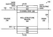
- FIGS. 1A and 1Bare partial cross-sectional views of a well-structure anti-punch-through microwire device.
- FIGS. 2A and 2Bare partial cross-sectional views of a first variation of the well-structure anti-punch-through microwire device of FIGS. 1A and 1B .
- FIGS. 3 through 5are partial cross-sectional views depicting steps in the fabrication of a completed well-structure microwire device.
- FIG. 6is a diagram depicting a silicon microwire growth process using a vapor-liquid-solid (VLS) approach.
- VLSvapor-liquid-solid
- FIG. 7is a diagram depicting a VLS Si microwire growth process using an alternate doping technique.
- FIG. 9depicts steps in the fabrication of an in-situ-doped microwire structure with shell layers of intrinsic Si, oxide, and conductive gate, based on a VLS-type growth process.
- FIG. 10is a flowchart illustrating a method for the fabrication of a well-structure anti-punch-through microwire device.
- FIGS. 1A and 1Bare partial cross-sectional views of a well-structure anti-punch-through microwire device.
- the device 100comprises a microwire 102 with alternating highly and lightly doped cylindrical regions, including a first dopant well-structure region 104 .
- a channel ring 106surrounds the well-structure region 104 , between source 108 and drain 110 regions of the microwire.
- the source and drain (S/D) regions 108 / 110are doped with a second dopant, opposite to the first dopant.
- the first dopantmay be n-type and the second dopant p-type.
- the first dopantmay be p-type and first dopant n-type.
- the microwire alternating highly and lightly doped cylindrical regionsare either an NPN or PNP sequence.
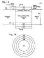
- FIGS. 2A and 2Bare partial cross-sectional views of a first variation of the well-structure anti-punch-through microwire device of FIGS. 1A and 1B .
- the microwire 102has an outer shell wall 200 , and the channel ring 106 is formed external to the microwire outer shell wall 200 .
- the channel ring 106is formed from an intrinsic or lightly doped silicon (Si) layer having a dopant concentration of less than about 2 ⁇ 10 16 per cubic centimeter (cm ⁇ 3 ).
- the well-structure region 104has a first dopant concentration of greater than about 5 ⁇ 10 16 cm ⁇ 3 , underlying the channel layer 106 .
- the channel ring 106has a ring thickness 202 in the range of 30 to 90 nm.
- the microwire 102has a diameter 204 of greater than 500 nanometers (nm).
- the above-described structurecan also be enabled using smaller microwires having a diameter of greater than 50 nm.
- the microwire 102may also be referred to as a nanowire.
- FIGS. 3 through 5are partial cross-sectional views depicting steps in the fabrication of a completed well-structure microwire device.
- the microwiresare grown (e.g., for PMOS devices) with modulated doping that defines highly-doped P + source and drain regions, and a moderately-doped N ⁇ “well” region that defines the device channel length.
- the N ⁇ dopingcan be constantly on for the entire growth cycle, with the P + doping being turned on and off (see FIG. 6 ).
- the catalyst materialis removed and an intrinsic Si shell is epitaxially grown on the surface of the microwire, see FIG. 3 .
- the layer thicknesscan be precisely controlled, thereby allowing full depletion of the channel region when the device is turned on.
- the intrinsic regioncan be oxidized using a variety of means, including wet or dry thermal oxidation, HDP oxidation, or depositing a CVD-based oxide. This oxide forms the gate insulator shell for the transistor device.
- FIG. 4depicts the device of FIG. 3 after etching of the outer shells (gate material, gate insulator, and intrinsic epi-Si).
- the wire diameteris shown to be greater than 500 nm is this example.
- FIG. 5depicts the final device configuration with electrode contacts.
- the current pathis indicated by dashed line.
- a PMOS device architectureis shown in this example.
- An NMOS devicewould require an N + -P ⁇ -N + doping profile.
- the highly doped P + regionsare contacted as the source and drain, while the intrinsic Si shell acts as the channel, and the N ⁇ region acts as an effective well between the source and drain (i.e., to prevent back-side conductance/leakage).
- the various shell layerscan be etched using an end-in etch process.
- the outer shell gate electrodecan be etched using this scheme through the contact holes.
- the channel lengthis controlled by the length of the N ⁇ well, as the intrinsic Si directly in contact with the P+ regions will likely experience some diffusion of dopant material during various high-temperature processing steps (e.g., oxidation).
- FIG. 7is a diagram depicting a VLS Si microwire growth process using an alternate doping technique. As shown, both the P + and N ⁇ are both pulse modulated. In this example, the modulation is complementary, however, in other aspects not shown, there may be periods of overlap when both the P + and N ⁇ dopant flow, or when neither the P + or N ⁇ dopant flow.
- VLS processis described, it should be understood that the microwires may be fabricated using other techniques, which may be more optimal for in-situ doping.
- the overall structureis independent of the growth process, provided that the Si material is effectively doped.
- This VLS processtypically uses gold as a catalyst, but other materials such as copper or aluminum have been reported as successful catalysts.
- Thick Si wirestypically have a 111 axial orientation, and in order to ensure good verticality normal to the substrate, 111 -normal Si growth wafers may be used.
- the catalystcan be deposited on the substrate either as a continuous film that is heated and agglomerated to form discrete balls, deposited over a patterned oxide/shadow mask to control the placement of the agglomerated balls, or deposited as functionalized particles.
- the catalyst ballsare etched from the ends of the microwires, and the microwires are harvested from the substrate, through an reactive ion etch (RIE)-and-undercut process, sonication, or other means known in the art.
- RIEreactive ion etch
- the harvested microwiresare then put in suspension and deposited onto a larger high-temperature-incompatible substrate (e.g., glass, metal, or plastic) using, for example, dielectrophoresis.
- the growth processuses doped silane, doped disilane, or doped chlorosilanes (e.g., SiCl 4 ) for the source material.
- FIG. 8depicts a conventional IC-based CMOS device on a bulk Si substrate (prior art).
- the microwiresare doped with alternating dopant concentrations and species, such that an example PMOS structure would have a heavily doped P + region (e.g., with boron as the dopant species), followed by an N ⁇ region (e.g., with a low concentration of phosphorous as the dopant), and then with another P + region.
- the basic doped microwire structuremimics the PMOS device of FIG. 8 , where the substrate is lightly doped N ⁇ and the source and drain regions are highly-doped P + .
- FIG. 9depicts steps in the fabrication of an in-situ-doped microwire structure with shell layers of intrinsic Si, oxide, and conductive gate, based on a VLS-type growth process.
- the catalyst material 600is formed on the substrate 602 and growth process is started (a).
- Dopant speciesare added during growth in such a way so as to have a sharp cut-off between the P + N ⁇ regions (b).
- the N ⁇ dopant speciescan be left on during the entire growth process (similar to a P + implant for PMOS devices fabricated on an N ⁇ substrate), see FIG. 6 . This process allows for an abrupt transition region between the two adjacent areas, within the limits imposed by the materials and growth processes themselves (e.g., depletion of dopant from the catalyst).
- the-wireis cleaned and an intrinsic Si layer is deposited over the surface of the wire to form a cylindrical shell (d).
- a perfect epitaxial siliconprovides a defect-free material for the channel portion of the microwire device (see FIG. 2 ).
- the thickness of the epitaxial Si layershould be sufficient to provide a 30 to 90 nm-thick channel, and after thermal oxidation (e), a 10 to 60 nm-thick gate insulator layer is formed.
- thermal oxidationthere might be significant dopant diffusion from the as-grown microwire into the intrinsic epi-Si layer.
- the oxidation process conditionscan be tailored so that diffusion from the lightly-doped well region is avoided.
- a heavier dopant speciessuch as As can be used that does not diffuse as readily as lighter elements.
- a low temperature high density plasma (HDP) or wet oxidation processcan be used to limit diffusion.
- a final conductive gate shellis deposited onto the microwire (f).
- the gate materialcan be any conductive layer that has an appropriate work function for device operation (e.g., P + Si, WN, or TaAlN). After the final shell is deposited, the wires are harvested and put into suspension with a compatible fluid.
- microwire of FIGS. 1A and 1Bmay be made in a similar manner, except that the step (Step d) of forming an intrinsic Si layer is omitted.
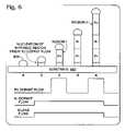
- FIG. 10is a flowchart illustrating a method for the fabrication of a well-structure anti-punch-through microwire device. Although the method is depicted as a sequence of numbered steps for clarity, the numbering does not necessarily dictate the order of the steps. It should be understood that some of these steps may be skipped, performed in parallel, or performed without the requirement of maintaining a strict order of sequence.
- the methodstarts at Step 1000 .
- Step 1002forms a microwire with alternating highly and lightly doped cylindrical regions (e.g., PNP or NPN sequences). As noted above, the microwire may have a diameter of greater than 500 nm, however the design is suitable for smaller nanowires (i.e. nanowires) having a diameter of greater than 50 nm.
- Step 1004forms a channel ring surrounding a first dopant well-structure region in the microwire, between source and drain regions of the microwire having a second dopant, opposite to the first dopant.
- Step 1006forms a gate dielectric ring surrounding the channel ring.
- Step 1008forms a gate electrode ring surrounding the gate dielectric ring.
- forming the microwire in Step 1002includes forming a microwire with an outer shell wall, and forming the channel ring in Step 1004 includes forming a channel ring external to the microwire outer shell wall.
- the channel ringis formed from an intrinsic silicon layer having a dopant concentration of less than about 2 ⁇ 10 16 per cubic centimeter (cm ⁇ 3 ), overlying a well-structure region having a first dopant concentration of greater than about 5 ⁇ 10 16 cm ⁇ 3 .
- the channeltypically has a ring thickness in the range of 30 to 90 nm.
- the gate dielectric ringtypically has a ring thickness in the range of 10 to 60 nm.
- Step 1002 adeposits a nucleation catalyst on a substrate to grow the microwire.
- Step 1002 bintroduces a silane precursor.
- Step 1002 cintroduces the first dopant, and Step 1002 d pulse modulates the introduction of the second dopant.
- Step 1002 cintroduces the second dopant and Step 1002 d pulse modulates the introduction of the first dopant.
- Step 1002 cpulse modulates the introduction of the second dopant in a first modulation cycle, while Step 1002 d pulse modulates the introduction of the first dopant in a second modulation cycle.
- the first and second modulation cyclesmay be complementary (opposite). Alternately, the cycles may overlap, or there may be gaps of no dopant introduction between cycles.
- forming the channel ring surrounding the first dopant well-structure regionincludes substeps. Subsequent to forming the nanowire, Step 1004 a removes the nucleation catalyst, and Step 1004 b epitaxially grows an intrinsic Si layer surrounding the microwire.
- Forming the gate dielectric ring surrounding the channel ring in Step 1006may include forming an oxidized Si layer overlying the intrinsic Si.
- a oxidized Si layeroverlying the intrinsic Si.
- HDPhigh density plasma
- CVDchemical vapor deposition
- Forming the gate electrode ring surrounding the gate dielectric ringmay include substeps.
- Step 1008 adeposits a gate electrode material overlying the oxidized intrinsic Si.
- Step 1008 bselectively etches the gate electrode material, oxidized intrinsic Si, and intrinsic Si layer surrounding the source and drain regions.
Landscapes
- Engineering & Computer Science (AREA)
- Chemical & Material Sciences (AREA)
- Nanotechnology (AREA)
- Physics & Mathematics (AREA)
- Mathematical Physics (AREA)
- Theoretical Computer Science (AREA)
- Crystallography & Structural Chemistry (AREA)
- Thin Film Transistor (AREA)
Abstract
Description
- 1. Field of the Invention
- This invention generally relates to integrated circuit (IC) fabrication and, more particularly, to a well-structure microwire transistor device.
- 2. Description of the Related Art
- As-grown, in-situ end-doped core-shell-shell (ECSS) nanowires are known for use in the fabrication of transistor devices. However, there are several problems associated with these wires, such as the ability to control the dopant concentration and width of the intrinsic channel, poor wire diameter and length uniformity, and harvesting of the nanowires (NWs) for dispersion onto a larger substrate.
- The NW wire diameter can affect the depth of the depletion layer within the transistor channel, and poor uniformity can cause some wires to be fully depleted, with adjacent wires only partially depleted. This is especially problematic for the control of threshold voltage distribution.
- It would be advantageous if the performance of NW transistor devices could be made more uniform.
- A microwire architecture is disclosed herein that permits the use of larger diameter wires having a fully-doped, modulated P-N-P, or N-P-N structure with an intrinsic epitaxial Si shell for NMOS or PMOS transistor applications. The use of larger diameters (dwire>500 nm) is desirable for a number of reasons. First, growth conditions are more favorable for larger diameter wires—providing a higher yield and greater uniformity. The use of an epitaxial intrinsic Si layer permits a finer control of the depletion region, so the devices can become fully depleted, enabling better control of the device parameters (e.g., threshold voltage) and uniformity. The modulated doping transient lengths (i.e., the growth length between when the source/drain dopant is on and off) have less impact on the overall device performance. The use of an epitaxial Si layer for the channel also permits precise threshold voltage adjustments to be made independent of the modulated growth process.
- Further, the effective channel width scales with the diameter, so that a 1 μm microwire has a channel width 10 times that of conventional nanowires with a typical diameter of approximately 100 nanometers (nm). Larger channel widths permit higher Ionper wire and reduce the need for multiple wires to be deposited per device.
- Accordingly, a method is provided for fabricating a well-structure anti-punch-through microwire device. The method initially forms a microwire with alternating highly and lightly doped cylindrical regions. A channel ring is formed surrounding a first dopant well-structure region in the microwire, between source and drain (S/D) regions of the microwire. The S/D regions are doped with a second dopant, opposite to the first dopant. A gate dielectric ring is formed surrounding the channel ring, and a gate electrode ring is formed surrounding the gate dielectric ring. The well-structure, in contrast to conventional micro or nanowire transistors, helps prevent the punch-through phenomena. In one aspect, the channel ring is formed external to the microwire outer shell wall.
- The microwire is formed by depositing a nucleation catalyst on a substrate. A silane precursor and the first dopant are introduced. As the microwire is grown, the introduction of the second dopant is pulse modulated. In another aspect, the introduction of both the first and second dopant is pulse modulated. For example, when the first dopant is introduced, the flow of the second dopant is stopped, and when the second dopant is introduced, the flow of the first dopant is interrupted. After removing the catalyst, an intrinsic Si layer is epitaxially grown surrounding the microwire, which may be used to form the channel ring. The intrinsic Si is oxidized to form the gate dielectric ring surrounding the channel ring. Then, a gate electrode material is deposited overlying the oxidized intrinsic Si, and the gate electrode material, oxidized intrinsic Si, and intrinsic Si layer surrounding the source and drain regions are selectively etched away.
- Additional details of the above-described method and well-structure anti-punch-through microwire device are presented below.
FIGS. 1A and 1B are partial cross-sectional views of a well-structure anti-punch-through microwire device.FIGS. 2A and 2B are partial cross-sectional views of a first variation of the well-structure anti-punch-through microwire device ofFIGS. 1A and 1B .FIGS. 3 through 5 are partial cross-sectional views depicting steps in the fabrication of a completed well-structure microwire device.FIG. 6 is a diagram depicting a silicon microwire growth process using a vapor-liquid-solid (VLS) approach.FIG. 7 is a diagram depicting a VLS Si microwire growth process using an alternate doping technique.FIG. 8 depicts a conventional IC-based CMOS device on a bulk Si substrate (prior art).FIG. 9 depicts steps in the fabrication of an in-situ-doped microwire structure with shell layers of intrinsic Si, oxide, and conductive gate, based on a VLS-type growth process.FIG. 10 is a flowchart illustrating a method for the fabrication of a well-structure anti-punch-through microwire device.FIGS. 1A and 1B are partial cross-sectional views of a well-structure anti-punch-through microwire device. Thedevice 100 comprises amicrowire 102 with alternating highly and lightly doped cylindrical regions, including a first dopant well-structure region 104. Achannel ring 106 surrounds the well-structure region 104, betweensource 108 and drain110 regions of the microwire. The source and drain (S/D)regions 108/110 are doped with a second dopant, opposite to the first dopant. For example, the first dopant may be n-type and the second dopant p-type. Alternately, the first dopant may be p-type and first dopant n-type. Thus, the microwire alternating highly and lightly doped cylindrical regions are either an NPN or PNP sequence.- A gate
dielectric ring 112 overlies thechannel ring 106. Typically, the gatedielectric ring 112 has aring thickness 114 in the range of 10 to 60 nm. Agate electrode ring 116 overlies the gatedielectric ring 112. FIGS. 2A and 2B are partial cross-sectional views of a first variation of the well-structure anti-punch-through microwire device ofFIGS. 1A and 1B . Themicrowire 102 has anouter shell wall 200, and thechannel ring 106 is formed external to the microwireouter shell wall 200.- Referencing any of the above-mentioned figures, the
channel ring 106 is formed from an intrinsic or lightly doped silicon (Si) layer having a dopant concentration of less than about 2×10¹⁶per cubic centimeter (cm−3). In contrast, the well-structure region 104 has a first dopant concentration of greater than about 5×1016cm−3, underlying thechannel layer 106. Whether thechannel ring 106 is formed internal or external to themicrowire 102, thechannel ring 106 has aring thickness 202 in the range of 30 to 90 nm. - In one aspect, the
microwire 102 has adiameter 204 of greater than 500 nanometers (nm). However, the above-described structure can also be enabled using smaller microwires having a diameter of greater than 50 nm. Themicrowire 102 may also be referred to as a nanowire. FIGS. 3 through 5 are partial cross-sectional views depicting steps in the fabrication of a completed well-structure microwire device. The microwires are grown (e.g., for PMOS devices) with modulated doping that defines highly-doped P+ source and drain regions, and a moderately-doped N− “well” region that defines the device channel length. The N− doping can be constantly on for the entire growth cycle, with the P+ doping being turned on and off (seeFIG. 6 ).- After microwire growth, the catalyst material is removed and an intrinsic Si shell is epitaxially grown on the surface of the microwire, see
FIG. 3 . The layer thickness can be precisely controlled, thereby allowing full depletion of the channel region when the device is turned on. The intrinsic region can be oxidized using a variety of means, including wet or dry thermal oxidation, HDP oxidation, or depositing a CVD-based oxide. This oxide forms the gate insulator shell for the transistor device. FIG. 4 depicts the device ofFIG. 3 after etching of the outer shells (gate material, gate insulator, and intrinsic epi-Si). The wire diameter is shown to be greater than 500 nm is this example.FIG. 5 depicts the final device configuration with electrode contacts. The current path is indicated by dashed line. A PMOS device architecture is shown in this example. An NMOS device would require an N+-P−-N+ doping profile. The highly doped P+ regions are contacted as the source and drain, while the intrinsic Si shell acts as the channel, and the N− region acts as an effective well between the source and drain (i.e., to prevent back-side conductance/leakage). The various shell layers can be etched using an end-in etch process. In particular, the outer shell gate electrode can be etched using this scheme through the contact holes. The channel length is controlled by the length of the N− well, as the intrinsic Si directly in contact with the P+ regions will likely experience some diffusion of dopant material during various high-temperature processing steps (e.g., oxidation).FIG. 6 is a diagram depicting a silicon microwire growth process using a vapor-liquid-solid (VLS) approach.Catalyst balls 600 are formed on a111Si substrate 602. N−-doped silane flows at appropriate growth conditions (temperature and pressure controlled) causing nucleation of an intrinsic Si microwire. The nucleation step can also be accomplished with intrinsic Si, followed by the addition of the N− dopant gas for the remainder of the growth. P+ dopant gas is turned on, providing heavily-doped source/drain region 1. The P+ dopant is stopped, providing lightly-doped N− “well” region. The P+ dopant is restarted for source/drain region 2. After sufficient growth, all gases are stopped and growth is terminated.FIG. 7 is a diagram depicting a VLS Si microwire growth process using an alternate doping technique. As shown, both the P+ and N− are both pulse modulated. In this example, the modulation is complementary, however, in other aspects not shown, there may be periods of overlap when both the P+ and N− dopant flow, or when neither the P+ or N− dopant flow.- Although a VLS process is described, it should be understood that the microwires may be fabricated using other techniques, which may be more optimal for in-situ doping. The overall structure is independent of the growth process, provided that the Si material is effectively doped. This VLS process typically uses gold as a catalyst, but other materials such as copper or aluminum have been reported as successful catalysts. Thick Si wires typically have a111 axial orientation, and in order to ensure good verticality normal to the substrate,111-normal Si growth wafers may be used. The catalyst can be deposited on the substrate either as a continuous film that is heated and agglomerated to form discrete balls, deposited over a patterned oxide/shadow mask to control the placement of the agglomerated balls, or deposited as functionalized particles.
- Following growth of the microwires, the catalyst balls are etched from the ends of the microwires, and the microwires are harvested from the substrate, through an reactive ion etch (RIE)-and-undercut process, sonication, or other means known in the art. The harvested microwires are then put in suspension and deposited onto a larger high-temperature-incompatible substrate (e.g., glass, metal, or plastic) using, for example, dielectrophoresis. The growth process uses doped silane, doped disilane, or doped chlorosilanes (e.g., SiCl4) for the source material.
FIG. 8 depicts a conventional IC-based CMOS device on a bulk Si substrate (prior art). As shown inFIGS. 6 and 7 , as the microwires are grown, they are doped with alternating dopant concentrations and species, such that an example PMOS structure would have a heavily doped P+ region (e.g., with boron as the dopant species), followed by an N− region (e.g., with a low concentration of phosphorous as the dopant), and then with another P+ region. The basic doped microwire structure mimics the PMOS device ofFIG. 8 , where the substrate is lightly doped N− and the source and drain regions are highly-doped P+.FIG. 9 depicts steps in the fabrication of an in-situ-doped microwire structure with shell layers of intrinsic Si, oxide, and conductive gate, based on a VLS-type growth process. Thecatalyst material 600 is formed on thesubstrate 602 and growth process is started (a). Dopant species are added during growth in such a way so as to have a sharp cut-off between the P+ N− regions (b). The N− dopant species can be left on during the entire growth process (similar to a P+ implant for PMOS devices fabricated on an N− substrate), seeFIG. 6 . This process allows for an abrupt transition region between the two adjacent areas, within the limits imposed by the materials and growth processes themselves (e.g., depletion of dopant from the catalyst).- After growth is completed, the catalyst ball is removed from the end of the microwire (c). This removal can be accomplished using a wet etch, provided that care is taken to avoid causing the microwires to stick to one another during the drying step (e.g., by using a critical-point-dryer). Example etches for a Au catalyst that do not affect the microwire itself might include HCl/HNO3, KI/I2, or NaCN.
- Following catalyst removal, the-wire is cleaned and an intrinsic Si layer is deposited over the surface of the wire to form a cylindrical shell (d). A perfect epitaxial silicon provides a defect-free material for the channel portion of the microwire device (see
FIG. 2 ). The thickness of the epitaxial Si layer should be sufficient to provide a 30 to 90 nm-thick channel, and after thermal oxidation (e), a 10 to 60 nm-thick gate insulator layer is formed. Depending on the conditions used for the thermal oxidation, there might be significant dopant diffusion from the as-grown microwire into the intrinsic epi-Si layer. The oxidation process conditions can be tailored so that diffusion from the lightly-doped well region is avoided. For example, a heavier dopant species such as As can be used that does not diffuse as readily as lighter elements. As another example, a low temperature high density plasma (HDP) or wet oxidation process can be used to limit diffusion. After oxidation of the epi-Si layer, a final conductive gate shell is deposited onto the microwire (f). The gate material can be any conductive layer that has an appropriate work function for device operation (e.g., P+ Si, WN, or TaAlN). After the final shell is deposited, the wires are harvested and put into suspension with a compatible fluid. - Note: the microwire of
FIGS. 1A and 1B may be made in a similar manner, except that the step (Step d) of forming an intrinsic Si layer is omitted. FIG. 10 is a flowchart illustrating a method for the fabrication of a well-structure anti-punch-through microwire device. Although the method is depicted as a sequence of numbered steps for clarity, the numbering does not necessarily dictate the order of the steps. It should be understood that some of these steps may be skipped, performed in parallel, or performed without the requirement of maintaining a strict order of sequence. The method starts atStep 1000.Step 1002 forms a microwire with alternating highly and lightly doped cylindrical regions (e.g., PNP or NPN sequences). As noted above, the microwire may have a diameter of greater than 500 nm, however the design is suitable for smaller nanowires (i.e. nanowires) having a diameter of greater than 50 nm.Step 1004 forms a channel ring surrounding a first dopant well-structure region in the microwire, between source and drain regions of the microwire having a second dopant, opposite to the first dopant.Step 1006 forms a gate dielectric ring surrounding the channel ring.Step 1008 forms a gate electrode ring surrounding the gate dielectric ring. In one aspect, forming the microwire inStep 1002 includes forming a microwire with an outer shell wall, and forming the channel ring inStep 1004 includes forming a channel ring external to the microwire outer shell wall.- Typically, the channel ring is formed from an intrinsic silicon layer having a dopant concentration of less than about 2×10¹⁶per cubic centimeter (cm−3), overlying a well-structure region having a first dopant concentration of greater than about 5×1016cm−3.
- Regardless of whether the channel ring is formed internal or external to the microwire, the channel typically has a ring thickness in the range of 30 to 90 nm. The gate dielectric ring typically has a ring thickness in the range of 10 to 60 nm.
- In one aspect, forming the microwire in
Step 1002 includes substeps.Step 1002adeposits a nucleation catalyst on a substrate to grow the microwire.Step 1002bintroduces a silane precursor.Step 1002cintroduces the first dopant, andStep 1002dpulse modulates the introduction of the second dopant. Alternately,Step 1002cintroduces the second dopant andStep 1002dpulse modulates the introduction of the first dopant. In another aspect,Step 1002cpulse modulates the introduction of the second dopant in a first modulation cycle, whileStep 1002dpulse modulates the introduction of the first dopant in a second modulation cycle. As shown inFIG. 7 , the first and second modulation cycles may be complementary (opposite). Alternately, the cycles may overlap, or there may be gaps of no dopant introduction between cycles. - In another aspect, forming the channel ring surrounding the first dopant well-structure region includes substeps. Subsequent to forming the nanowire,
Step 1004aremoves the nucleation catalyst, andStep 1004bepitaxially grows an intrinsic Si layer surrounding the microwire. - Forming the gate dielectric ring surrounding the channel ring in
Step 1006 may include forming an oxidized Si layer overlying the intrinsic Si. For example, wet thermal oxidation, dry thermal oxidation, or a high density plasma (HDP) process may be used to oxidize the intrinsic Si. Alternately, a chemical vapor deposition (CVD) process may be used to deposit oxidized Si overlying the intrinsic Si. Forming the gate electrode ring surrounding the gate dielectric ring may include substeps.Step 1008adeposits a gate electrode material overlying the oxidized intrinsic Si.Step 1008bselectively etches the gate electrode material, oxidized intrinsic Si, and intrinsic Si layer surrounding the source and drain regions. - A well-structure microwire transistor device has been provided. Examples of particular structural details, dimensions, and processes have been presented to illustrate the invention. However, the invention is not limited to merely these examples. Other variations and embodiments of the invention will occur to those skilled in the art.
Claims (21)
Priority Applications (2)
| Application Number | Priority Date | Filing Date | Title |
|---|---|---|---|
| US12/235,359US8153482B2 (en) | 2008-09-22 | 2008-09-22 | Well-structure anti-punch-through microwire device |
| PCT/JP2009/065622WO2010032653A1 (en) | 2008-09-22 | 2009-09-02 | Well-structure anti-punch-through microwire device, and fabrication method thereof |
Applications Claiming Priority (1)
| Application Number | Priority Date | Filing Date | Title |
|---|---|---|---|
| US12/235,359US8153482B2 (en) | 2008-09-22 | 2008-09-22 | Well-structure anti-punch-through microwire device |
Publications (2)
| Publication Number | Publication Date |
|---|---|
| US20100072455A1true US20100072455A1 (en) | 2010-03-25 |
| US8153482B2 US8153482B2 (en) | 2012-04-10 |
Family
ID=42036709
Family Applications (1)
| Application Number | Title | Priority Date | Filing Date |
|---|---|---|---|
| US12/235,359Expired - Fee RelatedUS8153482B2 (en) | 2008-09-22 | 2008-09-22 | Well-structure anti-punch-through microwire device |
Country Status (2)
| Country | Link |
|---|---|
| US (1) | US8153482B2 (en) |
| WO (1) | WO2010032653A1 (en) |
Cited By (6)
| Publication number | Priority date | Publication date | Assignee | Title |
|---|---|---|---|---|
| US20130320427A1 (en)* | 2012-06-04 | 2013-12-05 | Sematech, Inc. | Gated circuit structure with self-aligned tunneling region |
| US20160300886A1 (en)* | 2015-04-10 | 2016-10-13 | SK Hynix Inc. | Vertical transistor and variable resistive memory device including the same |
| US20170040419A1 (en)* | 2009-09-30 | 2017-02-09 | Mie Fujitsu Semiconductor Limited | Advanced Transistors with Punch Through Suppression |
| JP2019004131A (en)* | 2017-06-16 | 2019-01-10 | 富士通株式会社 | Compound semiconductor device, method of manufacturing the same, and receiver |
| WO2019223115A1 (en)* | 2018-05-24 | 2019-11-28 | 清华大学 | Nanowire transistor and fabrication method therefor |
| US11335785B2 (en)* | 2019-12-18 | 2022-05-17 | University Of Electronic Science And Technology Of China | Metal oxide semiconductor integrated circuit basic unit |
Families Citing this family (1)
| Publication number | Priority date | Publication date | Assignee | Title |
|---|---|---|---|---|
| CN109244072B (en)* | 2018-09-03 | 2021-05-18 | 芯恩(青岛)集成电路有限公司 | Semiconductor device structure and manufacturing method thereof |
Citations (11)
| Publication number | Priority date | Publication date | Assignee | Title |
|---|---|---|---|---|
| US3346414A (en)* | 1964-01-28 | 1967-10-10 | Bell Telephone Labor Inc | Vapor-liquid-solid crystal growth technique |
| US3493431A (en)* | 1966-11-25 | 1970-02-03 | Bell Telephone Labor Inc | Vapor-liquid-solid crystal growth technique |
| US3505127A (en)* | 1967-09-21 | 1970-04-07 | Bell Telephone Labor Inc | Vapor-liquid-solid crystal growth technique for the production of needle-like single crystals |
| US3573967A (en)* | 1967-03-01 | 1971-04-06 | Bell Telephone Labor Inc | Vapor-liquid-solid crystal growth technique |
| US5561308A (en)* | 1994-01-18 | 1996-10-01 | Kabushiki Kaisha Toshiba | Semiconductor device including thin film transistor |
| US5858862A (en)* | 1996-09-25 | 1999-01-12 | Sony Corporation | Process for producing quantum fine wire |
| US6768166B2 (en)* | 2001-06-26 | 2004-07-27 | Infineon Technologies Ag | Vertical transistor, memory arrangement and method for fabricating a vertical transistor |
| US20050136585A1 (en)* | 2003-12-23 | 2005-06-23 | Chau Robert S. | Method of fabricating semiconductor devices with replacement, coaxial gate structure |
| US20060175601A1 (en)* | 2000-08-22 | 2006-08-10 | President And Fellows Of Harvard College | Nanoscale wires and related devices |
| US20070017439A1 (en)* | 2005-07-12 | 2007-01-25 | Wenxu Xianyu | Method of fabricating orientation-controlled single-crystalline wire and method of fabricating transistor having the same |
| US7211464B2 (en)* | 2000-08-22 | 2007-05-01 | President & Fellows Of Harvard College | Doped elongated semiconductors, growing such semiconductors, devices including such semiconductors and fabricating such devices |
Family Cites Families (6)
| Publication number | Priority date | Publication date | Assignee | Title |
|---|---|---|---|---|
| JPH01307268A (en) | 1988-06-06 | 1989-12-12 | Nippon Telegr & Teleph Corp <Ntt> | Mis type transistor |
| JP2660446B2 (en) | 1990-01-12 | 1997-10-08 | 三菱電機株式会社 | Fine MIS type FET and manufacturing method thereof |
| JP3209876B2 (en) | 1995-02-16 | 2001-09-17 | 日精株式会社 | Multi-layer box-type circulation parking device |
| JP2004296628A (en) | 2003-03-26 | 2004-10-21 | Matsushita Electric Ind Co Ltd | Vertical field effect transistor and method of manufacturing the same |
| JP2005101278A (en) | 2003-09-25 | 2005-04-14 | Matsushita Electric Ind Co Ltd | Semiconductor device and manufacturing method thereof |
| JP2005197612A (en) | 2004-01-09 | 2005-07-21 | Sony Corp | Integrated quantum thin-line transistor, manufacturing method thereof, integrated thin-line transistor, manufacturing method thereof, and electronic application device |
- 2008
- 2008-09-22USUS12/235,359patent/US8153482B2/ennot_activeExpired - Fee Related
- 2009
- 2009-09-02WOPCT/JP2009/065622patent/WO2010032653A1/enactiveApplication Filing
Patent Citations (12)
| Publication number | Priority date | Publication date | Assignee | Title |
|---|---|---|---|---|
| US3346414A (en)* | 1964-01-28 | 1967-10-10 | Bell Telephone Labor Inc | Vapor-liquid-solid crystal growth technique |
| US3493431A (en)* | 1966-11-25 | 1970-02-03 | Bell Telephone Labor Inc | Vapor-liquid-solid crystal growth technique |
| US3573967A (en)* | 1967-03-01 | 1971-04-06 | Bell Telephone Labor Inc | Vapor-liquid-solid crystal growth technique |
| US3505127A (en)* | 1967-09-21 | 1970-04-07 | Bell Telephone Labor Inc | Vapor-liquid-solid crystal growth technique for the production of needle-like single crystals |
| US5561308A (en)* | 1994-01-18 | 1996-10-01 | Kabushiki Kaisha Toshiba | Semiconductor device including thin film transistor |
| US5858862A (en)* | 1996-09-25 | 1999-01-12 | Sony Corporation | Process for producing quantum fine wire |
| US20060175601A1 (en)* | 2000-08-22 | 2006-08-10 | President And Fellows Of Harvard College | Nanoscale wires and related devices |
| US7211464B2 (en)* | 2000-08-22 | 2007-05-01 | President & Fellows Of Harvard College | Doped elongated semiconductors, growing such semiconductors, devices including such semiconductors and fabricating such devices |
| US20090057650A1 (en)* | 2000-08-22 | 2009-03-05 | President And Fellows Of Harvard College | Nanoscale wires and related devices |
| US6768166B2 (en)* | 2001-06-26 | 2004-07-27 | Infineon Technologies Ag | Vertical transistor, memory arrangement and method for fabricating a vertical transistor |
| US20050136585A1 (en)* | 2003-12-23 | 2005-06-23 | Chau Robert S. | Method of fabricating semiconductor devices with replacement, coaxial gate structure |
| US20070017439A1 (en)* | 2005-07-12 | 2007-01-25 | Wenxu Xianyu | Method of fabricating orientation-controlled single-crystalline wire and method of fabricating transistor having the same |
Cited By (9)
| Publication number | Priority date | Publication date | Assignee | Title |
|---|---|---|---|---|
| US20170040419A1 (en)* | 2009-09-30 | 2017-02-09 | Mie Fujitsu Semiconductor Limited | Advanced Transistors with Punch Through Suppression |
| US10325986B2 (en)* | 2009-09-30 | 2019-06-18 | Mie Fujitsu Semiconductor Limited | Advanced transistors with punch through suppression |
| US20130320427A1 (en)* | 2012-06-04 | 2013-12-05 | Sematech, Inc. | Gated circuit structure with self-aligned tunneling region |
| US20160300886A1 (en)* | 2015-04-10 | 2016-10-13 | SK Hynix Inc. | Vertical transistor and variable resistive memory device including the same |
| US9691819B2 (en)* | 2015-04-10 | 2017-06-27 | SK Hynix Inc. | Vertical transistor and variable resistive memory device including the same |
| JP2019004131A (en)* | 2017-06-16 | 2019-01-10 | 富士通株式会社 | Compound semiconductor device, method of manufacturing the same, and receiver |
| WO2019223115A1 (en)* | 2018-05-24 | 2019-11-28 | 清华大学 | Nanowire transistor and fabrication method therefor |
| US11594623B2 (en) | 2018-05-24 | 2023-02-28 | Tsinghua University | Nanowire transistor and manufacturing method thereof |
| US11335785B2 (en)* | 2019-12-18 | 2022-05-17 | University Of Electronic Science And Technology Of China | Metal oxide semiconductor integrated circuit basic unit |
Also Published As
| Publication number | Publication date |
|---|---|
| US8153482B2 (en) | 2012-04-10 |
| WO2010032653A1 (en) | 2010-03-25 |
Similar Documents
| Publication | Publication Date | Title |
|---|---|---|
| US8153482B2 (en) | Well-structure anti-punch-through microwire device | |
| JP5273972B2 (en) | Field effect transistor and method of making field effect transistor | |
| JP5695255B2 (en) | Tunneling effect transistors based on elongated single crystal nanostructures with heterostructures | |
| US9159834B2 (en) | Faceted semiconductor nanowire | |
| US8422273B2 (en) | Nanowire mesh FET with multiple threshold voltages | |
| US8617970B2 (en) | Method of manufacturing semiconductor device | |
| JP5244126B2 (en) | Semiconductor nanostructure, semiconductor device and method for forming them | |
| CN104051535B (en) | Transistor containing the gate electrode for extending around one or more channel regions | |
| US10468505B2 (en) | Cylindrical germanium nanowire device | |
| CN101375398A (en) | nanowire tunneling transistor | |
| CN103956323A (en) | Semiconductor and manufacturing method thereof, and non-instantaneous computer readable storage medium | |
| CN101375380A (en) | Tunneling transistor with potential barrier | |
| TWI630719B (en) | Epitaxial structure, heterogeneous structure, nanowire lateral tunneling field effect transistor | |
| US20050161659A1 (en) | Nanowire and electronic device | |
| CN104009078B (en) | Nodeless mesh body pipe and manufacture method thereof | |
| CN106158636A (en) | Transistors and methods of forming them | |
| US20140308782A1 (en) | Self-limiting selective epitaxy process for preventing merger of semiconductor fins | |
| CN101310389B (en) | metal base nanowire transistor | |
| Leu et al. | Oxide-encapsulated vertical germanium nanowire structures and their DC transportproperties | |
| US9525026B2 (en) | Method of forming an epitaxial semiconductor layer in a recess and a semiconductor device having the same | |
| CN111627815B (en) | Methods for forming non-planar field effect transistors | |
| Nam et al. | A Bottom-up SiNW AMOSFET Fabrication Approach Giving SOI Level Performance | |
| JPH07273124A (en) | Bipolar transistor manufacturing method | |
| KR20090085443A (en) | Method for forming vertical nanowire semiconductor using nickel electrode and semiconductor using same |
Legal Events
| Date | Code | Title | Description |
|---|---|---|---|
| AS | Assignment | Owner name:SHARP LABORATORIES OF AMERICA, INC.,WASHINGTON Free format text:ASSIGNMENT OF ASSIGNORS INTEREST;ASSIGNOR:CROWDER, MARK ALBERT;REEL/FRAME:021567/0221 Effective date:20080919 Owner name:SHARP LABORATORIES OF AMERICA, INC., WASHINGTON Free format text:ASSIGNMENT OF ASSIGNORS INTEREST;ASSIGNOR:CROWDER, MARK ALBERT;REEL/FRAME:021567/0221 Effective date:20080919 | |
| STCF | Information on status: patent grant | Free format text:PATENTED CASE | |
| AS | Assignment | Owner name:SHARP KABUSHIKI KAISHA, JAPAN Free format text:ASSIGNMENT OF ASSIGNORS INTEREST;ASSIGNOR:SHARP LABORATORIES OF AMERICA INC.;REEL/FRAME:028211/0851 Effective date:20120515 | |
| FEPP | Fee payment procedure | Free format text:PAYOR NUMBER ASSIGNED (ORIGINAL EVENT CODE: ASPN); ENTITY STATUS OF PATENT OWNER: LARGE ENTITY | |
| FPAY | Fee payment | Year of fee payment:4 | |
| FEPP | Fee payment procedure | Free format text:MAINTENANCE FEE REMINDER MAILED (ORIGINAL EVENT CODE: REM.); ENTITY STATUS OF PATENT OWNER: LARGE ENTITY | |
| LAPS | Lapse for failure to pay maintenance fees | Free format text:PATENT EXPIRED FOR FAILURE TO PAY MAINTENANCE FEES (ORIGINAL EVENT CODE: EXP.); ENTITY STATUS OF PATENT OWNER: LARGE ENTITY | |
| STCH | Information on status: patent discontinuation | Free format text:PATENT EXPIRED DUE TO NONPAYMENT OF MAINTENANCE FEES UNDER 37 CFR 1.362 | |
| FP | Lapsed due to failure to pay maintenance fee | Effective date:20200410 |