US20100055807A1 - Plasma ashing apparatus and endpoint detection process - Google Patents
Plasma ashing apparatus and endpoint detection processDownload PDFInfo
- Publication number
- US20100055807A1 US20100055807A1US12/552,316US55231609AUS2010055807A1US 20100055807 A1US20100055807 A1US 20100055807A1US 55231609 AUS55231609 AUS 55231609AUS 2010055807 A1US2010055807 A1US 2010055807A1
- Authority
- US
- United States
- Prior art keywords
- plasma
- process chamber
- exhaust conduit
- free
- oxygen
- Prior art date
- Legal status (The legal status is an assumption and is not a legal conclusion. Google has not performed a legal analysis and makes no representation as to the accuracy of the status listed.)
- Granted
Links
- 238000000034methodMethods0.000titleclaimsabstractdescription220
- 230000008569processEffects0.000titleclaimsabstractdescription198
- 238000004380ashingMethods0.000titleclaimsabstractdescription99
- 238000001514detection methodMethods0.000titleclaimsabstractdescription22
- 239000007789gasSubstances0.000claimsabstractdescription141
- IJGRMHOSHXDMSA-UHFFFAOYSA-NAtomic nitrogenChemical compoundN#NIJGRMHOSHXDMSA-UHFFFAOYSA-N0.000claimsabstractdescription111
- 229910052760oxygenInorganic materials0.000claimsabstractdescription77
- QVGXLLKOCUKJST-UHFFFAOYSA-Natomic oxygenChemical compound[O]QVGXLLKOCUKJST-UHFFFAOYSA-N0.000claimsabstractdescription76
- 239000001301oxygenSubstances0.000claimsabstractdescription75
- 239000000758substrateSubstances0.000claimsabstractdescription75
- 229910052757nitrogenInorganic materials0.000claimsabstractdescription54
- 239000001257hydrogenSubstances0.000claimsabstractdescription50
- 229910052739hydrogenInorganic materials0.000claimsabstractdescription50
- 239000003989dielectric materialSubstances0.000claimsabstractdescription44
- OKTJSMMVPCPJKN-UHFFFAOYSA-NCarbonChemical compound[C]OKTJSMMVPCPJKN-UHFFFAOYSA-N0.000claimsabstractdescription41
- 229910052799carbonInorganic materials0.000claimsabstractdescription41
- UFHFLCQGNIYNRP-UHFFFAOYSA-NHydrogenChemical compound[H][H]UFHFLCQGNIYNRP-UHFFFAOYSA-N0.000claimsabstractdescription40
- 238000012544monitoring processMethods0.000claimsabstractdescription21
- 230000003287optical effectEffects0.000claimsabstractdescription21
- 229920002120photoresistant polymerPolymers0.000claimsdescription96
- 239000000463materialSubstances0.000claimsdescription53
- 230000001590oxidative effectEffects0.000claimsdescription33
- 239000001307heliumSubstances0.000claimsdescription32
- 229910052734heliumInorganic materials0.000claimsdescription32
- SWQJXJOGLNCZEY-UHFFFAOYSA-Nhelium atomChemical compound[He]SWQJXJOGLNCZEY-UHFFFAOYSA-N0.000claimsdescription32
- 239000000203mixtureSubstances0.000claimsdescription32
- 239000006227byproductSubstances0.000claimsdescription24
- 239000000376reactantSubstances0.000claimsdescription9
- 238000006243chemical reactionMethods0.000claimsdescription8
- 239000000047productSubstances0.000claimsdescription8
- 230000008859changeEffects0.000claimsdescription7
- 230000004044responseEffects0.000claimsdescription2
- 238000004891communicationMethods0.000abstractdescription16
- 239000012530fluidSubstances0.000abstractdescription14
- 238000001636atomic emission spectroscopyMethods0.000abstractdescription7
- 239000005416organic matterSubstances0.000abstractdescription5
- 210000002381plasmaAnatomy0.000description244
- 235000012431wafersNutrition0.000description62
- 241000894007speciesSpecies0.000description39
- 238000012545processingMethods0.000description19
- VYPSYNLAJGMNEJ-UHFFFAOYSA-NSilicium dioxideChemical compoundO=[Si]=OVYPSYNLAJGMNEJ-UHFFFAOYSA-N0.000description12
- 238000009826distributionMethods0.000description12
- CURLTUGMZLYLDI-UHFFFAOYSA-NCarbon dioxideChemical compoundO=C=OCURLTUGMZLYLDI-UHFFFAOYSA-N0.000description10
- 238000005530etchingMethods0.000description10
- 238000010438heat treatmentMethods0.000description9
- 125000004435hydrogen atomChemical group[H]*0.000description9
- 235000012239silicon dioxideNutrition0.000description9
- 229910002092carbon dioxideInorganic materials0.000description8
- 230000005855radiationEffects0.000description8
- 150000001875compoundsChemical class0.000description7
- 239000010453quartzSubstances0.000description7
- 229910052594sapphireInorganic materials0.000description7
- 239000010980sapphireSubstances0.000description7
- 238000011144upstream manufacturingMethods0.000description7
- XKRFYHLGVUSROY-UHFFFAOYSA-NArgonChemical compound[Ar]XKRFYHLGVUSROY-UHFFFAOYSA-N0.000description6
- 238000004140cleaningMethods0.000description6
- 239000012535impuritySubstances0.000description6
- 229910052751metalInorganic materials0.000description6
- 239000002184metalSubstances0.000description6
- 238000005192partitionMethods0.000description6
- 125000004429atomChemical group0.000description5
- 238000001816coolingMethods0.000description5
- 239000000539dimerSubstances0.000description5
- 239000010408filmSubstances0.000description5
- 229930195733hydrocarbonNatural products0.000description5
- 150000002430hydrocarbonsChemical class0.000description5
- 238000004519manufacturing processMethods0.000description5
- 230000036961partial effectEffects0.000description5
- 229920000642polymerPolymers0.000description5
- 229910001868waterInorganic materials0.000description5
- RYGMFSIKBFXOCR-UHFFFAOYSA-NCopperChemical compound[Cu]RYGMFSIKBFXOCR-UHFFFAOYSA-N0.000description4
- MYMOFIZGZYHOMD-UHFFFAOYSA-NDioxygenChemical compoundO=OMYMOFIZGZYHOMD-UHFFFAOYSA-N0.000description4
- 230000005540biological transmissionEffects0.000description4
- 229910052802copperInorganic materials0.000description4
- 239000010949copperSubstances0.000description4
- 229910001882dioxygenInorganic materials0.000description4
- 238000000295emission spectrumMethods0.000description4
- 210000000554irisAnatomy0.000description4
- 230000007246mechanismEffects0.000description4
- 230000001404mediated effectEffects0.000description4
- 229910052786argonInorganic materials0.000description3
- 230000015556catabolic processEffects0.000description3
- 229910010293ceramic materialInorganic materials0.000description3
- 238000002485combustion reactionMethods0.000description3
- 230000007423decreaseEffects0.000description3
- 238000006731degradation reactionMethods0.000description3
- 238000010790dilutionMethods0.000description3
- 239000012895dilutionSubstances0.000description3
- 238000005516engineering processMethods0.000description3
- 239000007943implantSubstances0.000description3
- 238000011065in-situ storageMethods0.000description3
- 229910052754neonInorganic materials0.000description3
- GKAOGPIIYCISHV-UHFFFAOYSA-Nneon atomChemical compound[Ne]GKAOGPIIYCISHV-UHFFFAOYSA-N0.000description3
- 239000004065semiconductorSubstances0.000description3
- 239000000126substanceSubstances0.000description3
- XLYOFNOQVPJJNP-UHFFFAOYSA-NwaterSubstancesOXLYOFNOQVPJJNP-UHFFFAOYSA-N0.000description3
- 239000004215Carbon black (E152)Substances0.000description2
- YZCKVEUIGOORGS-UHFFFAOYSA-NHydrogen atomChemical compound[H]YZCKVEUIGOORGS-UHFFFAOYSA-N0.000description2
- ATUOYWHBWRKTHZ-UHFFFAOYSA-NPropaneChemical compoundCCCATUOYWHBWRKTHZ-UHFFFAOYSA-N0.000description2
- 239000001569carbon dioxideSubstances0.000description2
- 239000000356contaminantSubstances0.000description2
- 239000002826coolantSubstances0.000description2
- 230000003247decreasing effectEffects0.000description2
- 238000013461designMethods0.000description2
- 230000001627detrimental effectEffects0.000description2
- 229910001873dinitrogenInorganic materials0.000description2
- 238000004868gas analysisMethods0.000description2
- 229910052736halogenInorganic materials0.000description2
- 239000011261inert gasSubstances0.000description2
- 239000011810insulating materialSubstances0.000description2
- 150000002500ionsChemical class0.000description2
- 150000002739metalsChemical class0.000description2
- VNWKTOKETHGBQD-UHFFFAOYSA-NmethaneChemical compoundCVNWKTOKETHGBQD-UHFFFAOYSA-N0.000description2
- 230000004048modificationEffects0.000description2
- 238000012986modificationMethods0.000description2
- 230000007935neutral effectEffects0.000description2
- 229910052756noble gasInorganic materials0.000description2
- 239000002245particleSubstances0.000description2
- -1poly(arylene ethersChemical class0.000description2
- 239000011148porous materialSubstances0.000description2
- 230000009257reactivityEffects0.000description2
- 230000002829reductive effectEffects0.000description2
- 230000003595spectral effectEffects0.000description2
- 238000012546transferMethods0.000description2
- 239000012780transparent materialSubstances0.000description2
- UGFAIRIUMAVXCW-UHFFFAOYSA-NCarbon monoxideChemical compound[O+]#[C-]UGFAIRIUMAVXCW-UHFFFAOYSA-N0.000description1
- 235000014653Carica parvifloraNutrition0.000description1
- 241000243321CnidariaSpecies0.000description1
- OTMSDBZUPAUEDD-UHFFFAOYSA-NEthaneChemical compoundCCOTMSDBZUPAUEDD-UHFFFAOYSA-N0.000description1
- YCKRFDGAMUMZLT-UHFFFAOYSA-NFluorine atomChemical compound[F]YCKRFDGAMUMZLT-UHFFFAOYSA-N0.000description1
- 239000004642PolyimideSubstances0.000description1
- 229910052782aluminiumInorganic materials0.000description1
- XAGFODPZIPBFFR-UHFFFAOYSA-NaluminiumChemical compound[Al]XAGFODPZIPBFFR-UHFFFAOYSA-N0.000description1
- PNEYBMLMFCGWSK-UHFFFAOYSA-Naluminium oxideInorganic materials[O-2].[O-2].[O-2].[Al+3].[Al+3]PNEYBMLMFCGWSK-UHFFFAOYSA-N0.000description1
- 238000004458analytical methodMethods0.000description1
- 239000005441auroraSubstances0.000description1
- 230000008901benefitEffects0.000description1
- UMIVXZPTRXBADB-UHFFFAOYSA-NbenzocyclobuteneChemical compoundC1=CC=C2CCC2=C1UMIVXZPTRXBADB-UHFFFAOYSA-N0.000description1
- 230000015572biosynthetic processEffects0.000description1
- 125000004432carbon atomChemical groupC*0.000description1
- 229910002091carbon monoxideInorganic materials0.000description1
- 239000000919ceramicSubstances0.000description1
- 238000005229chemical vapour depositionMethods0.000description1
- 239000002131composite materialSubstances0.000description1
- 239000000470constituentSubstances0.000description1
- 238000011109contaminationMethods0.000description1
- 230000008878couplingEffects0.000description1
- 238000010168coupling processMethods0.000description1
- 238000005859coupling reactionMethods0.000description1
- 239000013078crystalSubstances0.000description1
- 230000001419dependent effectEffects0.000description1
- 238000000151depositionMethods0.000description1
- 230000008021depositionEffects0.000description1
- 239000010432diamondSubstances0.000description1
- 238000009792diffusion processMethods0.000description1
- 230000009977dual effectEffects0.000description1
- 230000000694effectsEffects0.000description1
- 230000003628erosive effectEffects0.000description1
- 238000011156evaluationMethods0.000description1
- 230000005284excitationEffects0.000description1
- 229910052731fluorineInorganic materials0.000description1
- 239000011737fluorineSubstances0.000description1
- 239000005350fused silica glassSubstances0.000description1
- 230000004927fusionEffects0.000description1
- 238000005247getteringMethods0.000description1
- 239000011521glassSubstances0.000description1
- 230000009477glass transitionEffects0.000description1
- 150000002367halogensChemical class0.000description1
- 150000002431hydrogenChemical class0.000description1
- 230000006872improvementEffects0.000description1
- 238000007689inspectionMethods0.000description1
- 238000010849ion bombardmentMethods0.000description1
- 230000000670limiting effectEffects0.000description1
- 238000005259measurementMethods0.000description1
- VUZPPFZMUPKLLV-UHFFFAOYSA-Nmethane;hydrateChemical compoundC.OVUZPPFZMUPKLLV-UHFFFAOYSA-N0.000description1
- 125000002496methyl groupChemical group[H]C([H])([H])*0.000description1
- 238000004377microelectronicMethods0.000description1
- 229940028444museDrugs0.000description1
- QJGQUHMNIGDVPM-UHFFFAOYSA-Nnitrogen groupChemical group[N]QJGQUHMNIGDVPM-UHFFFAOYSA-N0.000description1
- 150000002835noble gasesChemical class0.000description1
- 239000011368organic materialSubstances0.000description1
- 229920000620organic polymerPolymers0.000description1
- 238000013021overheatingMethods0.000description1
- 239000007800oxidant agentSubstances0.000description1
- TWNQGVIAIRXVLR-UHFFFAOYSA-Noxo(oxoalumanyloxy)alumaneChemical compoundO=[Al]O[Al]=OTWNQGVIAIRXVLR-UHFFFAOYSA-N0.000description1
- 230000000737periodic effectEffects0.000description1
- 229920003209poly(hydridosilsesquioxane)Polymers0.000description1
- 229920000052poly(p-xylylene)Polymers0.000description1
- 229920001721polyimidePolymers0.000description1
- 230000001737promoting effectEffects0.000description1
- 239000001294propaneSubstances0.000description1
- GMVPRGQOIOIIMI-DWKJAMRDSA-Nprostaglandin E1Chemical compoundCCCCC[C@H](O)\C=C\[C@H]1[C@H](O)CC(=O)[C@@H]1CCCCCCC(O)=OGMVPRGQOIOIIMI-DWKJAMRDSA-N0.000description1
- 239000007845reactive nitrogen speciesSubstances0.000description1
- 239000003642reactive oxygen metaboliteSubstances0.000description1
- 230000006798recombinationEffects0.000description1
- 238000005215recombinationMethods0.000description1
- 230000009467reductionEffects0.000description1
- 230000001105regulatory effectEffects0.000description1
- 238000001275scanning Auger electron spectroscopyMethods0.000description1
- HBMJWWWQQXIZIP-UHFFFAOYSA-Nsilicon carbideChemical compound[Si+]#[C-]HBMJWWWQQXIZIP-UHFFFAOYSA-N0.000description1
- 229910010271silicon carbideInorganic materials0.000description1
- 239000000377silicon dioxideSubstances0.000description1
- 239000000243solutionSubstances0.000description1
- 125000006850spacer groupChemical group0.000description1
- 229910001220stainless steelInorganic materials0.000description1
- 239000010935stainless steelSubstances0.000description1
- 230000003068static effectEffects0.000description1
- 238000012360testing methodMethods0.000description1
- 238000002076thermal analysis methodMethods0.000description1
- 239000010409thin filmSubstances0.000description1
- 230000007704transitionEffects0.000description1
- 229910052721tungstenInorganic materials0.000description1
- 239000010937tungstenSubstances0.000description1
Images


Classifications
- H—ELECTRICITY
- H01—ELECTRIC ELEMENTS
- H01L—SEMICONDUCTOR DEVICES NOT COVERED BY CLASS H10
- H01L21/00—Processes or apparatus adapted for the manufacture or treatment of semiconductor or solid state devices or of parts thereof
- H01L21/67—Apparatus specially adapted for handling semiconductor or electric solid state devices during manufacture or treatment thereof; Apparatus specially adapted for handling wafers during manufacture or treatment of semiconductor or electric solid state devices or components ; Apparatus not specifically provided for elsewhere
- H01L21/67005—Apparatus not specifically provided for elsewhere
- H01L21/67242—Apparatus for monitoring, sorting or marking
- H01L21/67253—Process monitoring, e.g. flow or thickness monitoring
- G—PHYSICS
- G03—PHOTOGRAPHY; CINEMATOGRAPHY; ANALOGOUS TECHNIQUES USING WAVES OTHER THAN OPTICAL WAVES; ELECTROGRAPHY; HOLOGRAPHY
- G03F—PHOTOMECHANICAL PRODUCTION OF TEXTURED OR PATTERNED SURFACES, e.g. FOR PRINTING, FOR PROCESSING OF SEMICONDUCTOR DEVICES; MATERIALS THEREFOR; ORIGINALS THEREFOR; APPARATUS SPECIALLY ADAPTED THEREFOR
- G03F7/00—Photomechanical, e.g. photolithographic, production of textured or patterned surfaces, e.g. printing surfaces; Materials therefor, e.g. comprising photoresists; Apparatus specially adapted therefor
- G03F7/26—Processing photosensitive materials; Apparatus therefor
- G03F7/42—Stripping or agents therefor
- G03F7/427—Stripping or agents therefor using plasma means only
- H—ELECTRICITY
- H01—ELECTRIC ELEMENTS
- H01J—ELECTRIC DISCHARGE TUBES OR DISCHARGE LAMPS
- H01J37/00—Discharge tubes with provision for introducing objects or material to be exposed to the discharge, e.g. for the purpose of examination or processing thereof
- H01J37/32—Gas-filled discharge tubes
- H01J37/32009—Arrangements for generation of plasma specially adapted for examination or treatment of objects, e.g. plasma sources
- H01J37/32357—Generation remote from the workpiece, e.g. down-stream
- H—ELECTRICITY
- H01—ELECTRIC ELEMENTS
- H01J—ELECTRIC DISCHARGE TUBES OR DISCHARGE LAMPS
- H01J37/00—Discharge tubes with provision for introducing objects or material to be exposed to the discharge, e.g. for the purpose of examination or processing thereof
- H01J37/32—Gas-filled discharge tubes
- H01J37/32431—Constructional details of the reactor
- H01J37/32798—Further details of plasma apparatus not provided for in groups H01J37/3244 - H01J37/32788; special provisions for cleaning or maintenance of the apparatus
- H01J37/32816—Pressure
- H01J37/32834—Exhausting
- H—ELECTRICITY
- H01—ELECTRIC ELEMENTS
- H01J—ELECTRIC DISCHARGE TUBES OR DISCHARGE LAMPS
- H01J37/00—Discharge tubes with provision for introducing objects or material to be exposed to the discharge, e.g. for the purpose of examination or processing thereof
- H01J37/32—Gas-filled discharge tubes
- H01J37/32917—Plasma diagnostics
- H01J37/32935—Monitoring and controlling tubes by information coming from the object and/or discharge
- H—ELECTRICITY
- H01—ELECTRIC ELEMENTS
- H01L—SEMICONDUCTOR DEVICES NOT COVERED BY CLASS H10
- H01L21/00—Processes or apparatus adapted for the manufacture or treatment of semiconductor or solid state devices or of parts thereof
- H01L21/67—Apparatus specially adapted for handling semiconductor or electric solid state devices during manufacture or treatment thereof; Apparatus specially adapted for handling wafers during manufacture or treatment of semiconductor or electric solid state devices or components ; Apparatus not specifically provided for elsewhere
- H01L21/67005—Apparatus not specifically provided for elsewhere
- H01L21/67011—Apparatus for manufacture or treatment
- H01L21/67017—Apparatus for fluid treatment
- H01L21/67063—Apparatus for fluid treatment for etching
- H01L21/67069—Apparatus for fluid treatment for etching for drying etching
- H—ELECTRICITY
- H01—ELECTRIC ELEMENTS
- H01J—ELECTRIC DISCHARGE TUBES OR DISCHARGE LAMPS
- H01J2237/00—Discharge tubes exposing object to beam, e.g. for analysis treatment, etching, imaging
- H01J2237/32—Processing objects by plasma generation
- H01J2237/33—Processing objects by plasma generation characterised by the type of processing
- H01J2237/334—Etching
- H01J2237/3342—Resist stripping
Definitions
- the present disclosurerelates to semiconductor apparatuses and processes, and more particularly, to plasma mediated processes and plasma apparatuses suitable for ashing organic material from a substrate including a low k dielectric material.
- Low k dielectric materials used in advanced integrated circuitstypically comprise organic polymers or oxides and have dielectric constants less than about 3.5.
- the low k dielectric materialscan be spun onto the substrate as a solution or deposited by a chemical vapor deposition process.
- Important low k film propertiesinclude thickness and uniformity, dielectric constant, refractive index, adhesion, chemical resistance, thermal stability, pore size and distribution, coefficient of thermal expansion, glass transition temperature, film stress, and copper diffusion coefficient.
- the wafersare generally subjected to many process steps before finished integrated circuits can be produced.
- Low k dielectric materialsespecially carbon containing low k dielectric materials, can be sensitive to some of these process steps.
- plasma used during an “ashing” stepcan strip both photoresist materials as well as remove a portion of the low-k dielectric film.
- Ashingrefers to a plasma mediated stripping process by which photoresist and post etch residues are stripped or removed from a substrate upon exposure to the plasma.
- the ashing processgenerally occurs after an etching or implant process has been performed in which a photoresist material is used as a mask for etching a pattern into the underlying substrate or for selectively implanting ions into the exposed areas of the substrate.
- the remaining photoresist and any post etch or post implant residues on the wafer after the etch process or implant process is completemust be removed prior to further processing for numerous reasons generally known to those skilled in the art.
- the ashing stepis typically followed by a wet chemical treatment to remove traces of the residue, which can cause further degradation of the low k dielectric, loss of material, and may also cause increase in the dielectric constant.
- ashing processessignificantly differ from etching processes. Although both processes may be plasma mediated, an etching process is markedly different in that the plasma chemistry is chosen to permanently transfer an image into the substrate by removing portions of the substrate surface through openings in a photoresist mask.
- the plasmagenerally includes high-energy ion bombardment at low temperatures and low pressures (on the order of milli-Torrs) to remove portions of the substrate.
- the portions of the substrate exposed to the ionsare generally removed at a rate equal to or greater than the removal rate of the photoresist mask.
- ashing processesgenerally refer to selectively removing the photoresist mask and any polymers or residues formed during etching.
- the ashing plasma chemistryis much less aggressive than etching chemistries and is generally chosen to remove the photoresist mask layer at a rate much greater than the removal rate of the underlying substrate. Moreover, most ashing processes heat the substrate to temperatures greater than 200° C. to increase the plasma reactivity, and are performed at pressures of about 1.0 Torr. Thus, etching and ashing processes are directed to removal of significantly different materials and as such, require completely different plasma chemistries and processes. Successful ashing processes are not used to permanently transfer an image into the substrate. Rather, successful ashing processes are defined by the photoresist, polymer and residue removal rates without affecting or removing underlying layers, e.g., low k dielectric layers.
- the use of oxygen-containing plasma dischargesis generally less preferred for advanced device fabrication employing copper metal layers since copper metal is readily oxidized at the elevated temperatures typically employed for photoresist ashing.
- the damageis not detected during metrology inspection of the substrate after plasma processing.
- the damagecan be readily demonstrated by a subsequent wet cleaning process, as may be typically employed after plasma ashing, wherein portions of the carbon and/or hydrogen-containing low k dielectric material are removed.
- the removed portions of the dielectric materialare a source of variation in the critical dimension (CD) of the feature that is frequently unacceptable and impacts overall device yield.
- the electrical and mechanical properties of the dielectric materialmay be changed by exposure to the oxygen-free plasma discharges thereby affecting operating performance. It is believed that carbon is depleted from the dielectric material during the plasma exposure.
- the ashing plasmashould not affect the underlying low k dielectric layers and preferably removes only the photoresist material.
- SiO 2as the dielectric material provided high selectivity with these gas sources.
- oxygen and nitrogen free plasma processeshave been developed. One such process includes generating plasma from a gas mixture comprising helium and hydrogen. However, the mechanism of removal is different for these less aggressive plasma discharges.
- the oxygen and nitrogen free plasmasuch as the plasma formed from helium and hydrogen does not ash the photoresist in the traditional sense. Rather, it is believed that the plasma causes portions of the photoresist to sublime from the substrate.
- the plasma exposuretends to deposit large bodies of the sublimed photoresist and byproducts within the processing chamber and in areas downstream from the plasma process chamber such as in the throttle valve and exhaust lines.
- the buildup of these ashing materialscan lead to short mean-time-between-clean (MTBC) times and frequent rebuild/replacement of vacuum hardware resulting in loss of throughput and increased costs of ownership.
- MTBCmean-time-between-clean
- deposits of photoresist material within the process chamber that are located above the plane of the substratecan lead to particulate contamination on the substrate, thereby further affecting device yields.
- a plasma ashing apparatusfor removing photoresist and/or post etch residues from a substrate, comprising a first gas source; a plasma generating component in fluid communication with the first gas source, wherein the plasma generating component generates a first plasma for selectively removing the photoresist and/or post etch residues from the substrate; a process chamber in fluid communication with the plasma generating component for receiving the plasma, wherein the process chamber contains the substrate; an exhaust conduit in fluid communication with the process chamber; wherein the exhaust conduit comprises a port for introducing a second gas source and an afterburner assembly coupled to the exhaust conduit, wherein the port is disposed intermediate to the process chamber and the afterburner assembly; and an optical detection system coupled to the exhaust conduit comprising collection optics focused within a plasma discharge region of the afterburner assembly.
- a downstream plasma ashing and/or residue removal apparatuscomprises means for generating a plasma in an exhaust conduit in fluid communication with a process chamber; means for monitoring an emission signal for species generated within the plasma; and means for determining an endpoint of a plasma ashing and/or residue removal process on a substrate in the process chamber from the emission signal produced in the exhaust conduit.
- a method for detecting an endpoint for an oxygen free and nitrogen free plasma ashing processcomprising exposing a substrate comprising photoresist material and/or post etch residues thereon to the oxygen free and nitrogen free plasma in a process chamber; removing the photoresist material and/or post etch residues from the substrate; exhausting the removed photoresist material and/or post etch residues from the process chamber into an exhaust conduit fluidly coupled to the process chamber; selectively introducing an oxidizing gas into the exhaust conduit; generating an oxygen containing plasma from the oxidizing gas and the exhausted photoresist material and/or post etch residues to form emissive species; and optically monitoring an emission signal produced by the emissive species to determine the endpoint of the oxygen free and nitrogen free plasma ashing.
- an endpoint detection process for an oxygen free and nitrogen free plasma ashing process for removing photoresist and/or residues from a substratecomprising introducing an oxidizing gas and a plasma ashing discharge into an exhaust conduit of a plasma asher apparatus, wherein the plasma ashing discharge comprises photoresist material, post etch residues, and post ashing products, and wherein the plasma ashing discharge is free from atomic nitrogen and atomic oxygen species; generating a plasma from the oxidizing gas and the plasma ashing discharge to form emissive species; and optically monitoring an emission signal intensity correlating to the emissive species, wherein an endpoint of the oxygen free and nitrogen free plasma ashing process is detected when the emission signal intensity correlating to the emissive species is no longer present.
- a method for determining an endpoint of an oxygen fee and nitrogen free plasma ashing process used for stripping photoresist material from a substrate having a carbon containing low k dielectric materialcomprising exposing the substrate to the oxygen free and nitrogen free plasma ashing process in a process chamber to remove the photoresist material from the substrate and form volatile byproducts; exhausting the photoresist material and volatile byproducts from the process chamber into an exhaust conduit; selectively introducing an oxidizing gas into the exhaust conduit, wherein the oxidizing gas does not flow into the process chamber; generating a plasma in the exhaust conduit from oxidizing gas, the exhausted photoresist material, and the volatile byproducts; measuring an emission signal intensity in the exhaust conduit correlating to a wavelength of about 283 nm, 309 nm, about 387 nm, about 431 nm, about 434 nm, about 468 nm, about 472 nm, about 513 nm, about 516 nm, about 656
- a method for determining an endpoint of an oxygen fee and nitrogen free plasma ashing process used for stripping photoresist material from a substrate having a carbon containing low k dielectric materialcomprising generating a first plasma in a process chamber in the absence of oxygen and nitrogen from a gas mixture comprising hydrogen or helium or a combination comprising at least one of the foregoing gases; exposing the substrate provided in the process chamber to the first plasma to selectively remove photoresist material and/or residues from the substrate; exhausting the removed photoresist material and/or residues from the process chamber into an exhaust conduit;
- FIG. 1is a cross sectional view of a downstream plasma ashing apparatus
- FIG. 2shows a perspective view of a microwave enclosure for use in a plasma asher apparatus
- FIG. 3shows a cross sectional view which schematically shows a plasma generating component suitable for use with the downstream plasma ashing apparatus
- FIG. 4shows perspective view of the plasma ashing apparatus
- FIG. 5is a partial cutaway perspective view of a photoresist asher process chamber into which is installed a gas distribution system;
- FIG. 6is a plan view of the gas distribution system in accordance with one embodiment
- FIG. 7is a sectional view of the baffle plate assembly of FIG. 6 , taken along lines 6 - 6 ;
- FIG. 8is a plan view of the gas distribution system in accordance with another embodiment.
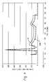
- FIG. 9is a graph illustrating a time evolution of a light intensity emitted for OH species generated from sublimated organic matter removed from a wafer due to heating the wafer to a temperature of 300° C. in an oxygen free and nitrogen free environment and oxidized in an exhaust conduit of a plasma ashing apparatus;
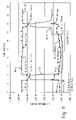
- FIG. 10is a graph illustrating a time evolution of carbon dioxide partial pressure as measured with a residual gas analyzer in an oxygen free and nitrogen free plasma and oxidized in an exhaust conduit of a plasma ashing apparatus;
- FIG. 11is a graph illustrating residual gas analysis of partial pressures for helium, nitrogen, and oxygen measured upstream from the afterburner and inlet for introducing oxygen gas into an exhaust conduit of a plasma asher apparatus (i.e., downstream from the wafer process chamber), wherein the flow rate of helium is varied;
- FIG. 12is a time evolution of optical signals showing various photoresist constituents (O and CN) and product (OH) produced upon stepwise heating of a photoresist-coated wafer;
- FIG. 13is a time evolution of a DUV photoresist removal process using a hydrogen/helium ashing process without employing an oxidizing gas in the endpoint monitoring process;
- FIG. 14is a time evolution of a DUV photoresist removal process using a hydrogen/helium ashing process and employing an oxidizing gas in the endpoint monitoring process;
- FIG. 15is a time evolution of an I-line photoresist removal process using a hydrogen/helium ashing process and employing an oxidizing gas in the endpoint monitoring process.
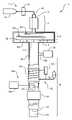
- FIG. 1generally illustrates an axial flow downstream plasma apparatus 10 suitable for use in removing photoresist, sidewall deposits, and post etch residues from substrates including low k dielectric materials.
- the plasma apparatus 10generally comprises a gas delivery component 12 , a plasma-generating component 14 , a processing chamber 16 , and an exhaust assembly component 18 .
- the various componentsin combination, provide improvements in processing substrates with oxygen free and nitrogen free plasma discharges, wherein the substrates include carbon containing low k dielectric materials.
- Downstream axial flow plasma apparatuses particularly suitable for modification in the present disclosureare plasma ashers, such as for example, those microwave plasma ashers available under the trade name Fusion ES3LK and commercially available from Axcelis Technologies Corporation. Portions of the microwave plasma asher are described in U.S. Pat. Nos. 5,498,308 and 4,341,592, and PCT International Application No. WO/97/37055, herein incorporated by reference in their entireties. As will be discussed below, the disclosure is not limited to any particular plasma asher in this or in the following embodiments. For instance, an inductively or capacitively coupled plasma reactor can be used.
- Carbon-containing low k dielectricsare hereinafter defined as those carbon containing insulating materials suitable for use in the manufacture of integrated circuits or the like having a dielectric constant less than about 3.5, with a dielectric constant less than about 3.0 more preferred.
- the carbon-containing low k dielectric materialsmay include pendant groups that contain carbon or may be carbon-containing wherein the backbone of the dielectric material is primarily comprised of an interconnecting network of carbon.
- Carbon-containing low k dielectricscan generally be categorized as one of two types: organic and doped oxides.
- organic low k dielectric materialsinclude polyimides, benzocyclobutene, parylenes, diamond-like carbon, poly(arylene ethers), cyclotenes, fluorocarbons and the like, such as those dielectrics commercially available under the trademarks SiLK, or BCB.
- doped oxide low k dielectric materialsinclude methyl silsesquioxane, hydrogen silsesquioxanes, nanoporous oxides, carbon doped silicon dioxides, and the like, such as, for example, those dielectrics commercially available under the trademarks CORAL, BLACK DIAMOND and AURORA. Both types of carbon-containing low-k materials exist in dense and porous versions. Porous versions thereof are commercially known under trademarks such as LKD, ORION, BOSS, or porous SiLK. Other carbon-containing low k dielectric materials will be apparent to one of ordinary skill in the art in view of this disclosure.
- hydrogen containing low k dielectricsare hereinafter defined as those hydrogen containing insulating materials suitable for use in the manufacture of integrated circuits or the like having a dielectric constant less than about 3.5.
- Many of the carbon containing low k dielectrics described aboveinclude one or more hydrogen atoms attached to the carbon atoms within its chemical structure.
- suitable hydrogen containing low k dielectric materials in the present disclosureare not intended to be limited to carbon containing structures.
- the gas delivery component 12preferably comprises a gas purifier 20 in fluid communication with a gas source 22 (for generating the oxygen free and nitrogen free plasma) and a gas inlet 24 of the plasma-generating component 14 .
- An additional gas source(not shown) may be in fluid communication with the gas inlet 24 for providing in situ cleaning capabilities. In situ cleaning is a process for cleaning the process chamber 16 using the plasma source as opposed to manually cleaning the chamber components by disassembling a portion of the process chamber for access thereto.
- the purifier 20is adapted to reduce the level of impurities to less than about 10 parts per million (ppm), with impurity levels less than about 5 ppm more preferred, with impurity levels less than about 1 ppm more preferred, and with less than about 100 parts per billion (ppb) most preferred.
- Suitable purifiers achieving these impurity levelsinclude those based on a metal gettering technology such as those gas purifiers commercially available under the trade name MONO TORR®. high flow purifiers from SAES Pure Gas, Inc.
- gas purifier 20in fluid communication with the gas source 22 employed for forming the plasma reduces the level of contaminants to amounts effective for robust processing of low k dielectric substrates, and in particular, carbon-containing low k dielectrics.
- gases for generating the oxygen free and nitrogen free plasmainclude, but are not intended to be limited to, hydrogen, helium, argon, neon, other inert gases, hydrocarbons, and combinations comprising one or more of the foregoing gases.
- a helium gas source having a reported purity of 99.999%can be undesirable for plasma mediated processing of carbon-containing low k dielectrics.
- Impurities such as H 2 O, O 2 , CO, CO 2 , and N 2can be at levels sufficient to cause erosion of the low k dielectric during further processing of the substrate and/or deleteriously cause an increase in the dielectric constant.
- the incoming gas for forming the plasmais purified to contain less than 100 ppb of H 2 O, O 2 , CO, CO 2 , and N 2 .
- the purifier 20is preferably selected to be efficient and provide these preferred impurity levels at relatively high flow rates, e.g., flow rates of about 100 to about 12,000 standard cubic centimeters per minute (sccm) or more can be expected for a 3.00 mm downstream plasma asher.
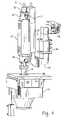
- FIGS. 2 and 3illustrate an exemplary microwave plasma-generating component 14 with which the present disclosure may be practiced.
- FIG. 4illustrates a perspective view of the plasma ashing apparatus 10 including the microwave plasma-generating component and a perspective view of the process chamber 16 .
- the plasma-generating component 14has been simplified to illustrate only those components that are relevant to an understanding of the present disclosure. Those of ordinary skill in the art will recognize that other components may be required to produce an operational plasma ashing apparatus 10 . However, because such components are well known in the art, and because they do not further aid in the understanding of the present disclosure, a discussion of such components is not provided.
- the microwave plasma-generating component 14includes a microwave enclosure 24 .
- the microwave enclosure 24is a rectangular box that is partitioned using lengthwise sections 26 , 28 , and 30 having plasma tube 32 passing therethrough. Each partition has an opening through which the plasma tube passes.
- Each sectionis fed with microwave energy during operation. Thus, each section appears to be a relatively short cavity to the incoming microwave energy, promoting the formation of modes having azithumal and axial uniformity.
- Outer tube 34surrounds the plasma tube inside the cavity. The outer tube is slightly separated from the plasma tube and air, under positive pressure, is fed between the two tubes to provide effective cooling of the plasma tube.
- Tube 32is preferably made of sapphire. Other plasma tube materials such as quartz or alumina-coated quartz or other ceramic materials can be used.
- the microwave enclosure 24is dimensioned to support the rectangular TM 110 mode and the enclosure 24 may have a square cross section.
- the dimensions of the cross sectionsare such that the TM 110 mode is resonant.
- the length of each sectionis less than ⁇ g/2 where ⁇ g is the guide length within the cavity of the TE 104 mode.
- the openings in the partitions 26 , 28 , and 30 through which the concentric tubes are fedare made larger than the exterior dimension of the plasma tube.
- an iris plate 36which covers the open side of the microwave structure and is effective to feed microwave energy into adjacent sections.
- Plate 36is a flat metallic plate having irises 38 , 40 , 42 , 44 , through which the microwave energy is fed.
- irises 38 , 40 , 42 , 44There is microwave transmission through these irises, which causes plasma to be excited in the part of the tube that is surrounded by the partition.
- Such transmissionhelps reduce thermal gradients in the plasma tube between regions surrounded by partitions and regions that are not. If an outer tube is not used (cooling provided in some other manner) the openings in the partition are sized so that there is a space between the plasma tube and the partition to provide such microwave transmission.
- Microwave traps 46 and 48are provided at the ends to prevent microwave transmission. Such traps may be of the type disclosed in U.S. Pat. No. 5,498,308. Air seals/directional feeders 50 and 52 are provided for admitting cooling air and feeding it to the space between the concentric tubes. Air seals/directional feeder 54 are shown at the outlet end and a fourth such unit is present but is not seen.
- Magnetron 56provides microwave power that is fed through coupler 58 to a waveguide supplying TE 10 mode, having mutually perpendicular sections 60 and 62 .
- the length of waveguide section 62is adjustable with moveable plunger 64 .
- the bottom plate of waveguide section 62is iris plate 36 , which couples microwave energy into partitioned microwave structure 24 , through which the plasma tube 32 extends; thus plasma is excited in the gas mixture flowing through the plasma tube.
- end cap 70abuts microwave trap 48 , and fitting 74 having a central orifice for admitting gas to the plasma tube extends into the end cap.
- the gas supply 22is regulated by an external flow box (not shown).
- the gas purifier 20is disposed in fluid communication with the gas supply 22 and the gas inlet 23 (see FIG. 1 ).
- the plasma tube 32is supported at this end by “o” ring 72 in the end cap.
- the outer tube 34is supported at its ends by abutment against microwave traps 46 and 48 .
- Spacer 76is present to provide the proper spacing in relation to the process chamber.
- the other end of the plasma tubeis located in end member 78 , and has an opening 80 for emitting plasma/gas into the process chamber 16 .
- the conduit forming the opening 80is fitted with a narrow aperture fitting to create a pressure differential between the plasma tube 32 and the processing chamber 16 , wherein the pressure is greater in the plasma tube 32 .
- the pressure within the plasma tube 32preferably ranges from about 1 torr to about atmospheric pressure.
- the pressure within the process chamber during operationranges from about 100 millitorr to about atmospheric pressure.
- the opening 80 of the plasma tube 32is in fluid communication with an interior region of the process chamber 16 . Since the plasma is discharged from a relatively narrow orifice (compared to the dimensions of the substrate to be processed) into the interior of the process chamber, a gas distribution system 100 to promote uniform plasma exposure onto the substrate is disposed within the process chamber 16 . The gas distribution system 100 is disposed intermediate to the substrate and opening 80 of the plasma tube 32 .
- the gas distribution system 100comprises one or more baffle plates above the wafer to promote even distribution of the plasma to the substrate surface.
- the baffle platespreferably include multiply stacked baffle plates, wherein each plate contains one or more apertures.
- a plenumis formed between the baffle plate assembly and the upper wall of the process chamber.
- the baffle plate assemblyis adapted to provide more uniform concentration of reactive species from the plasma to the wafer surface.
- the reduction in activity of hydrogen radicals as these species flow to the outer edges of the baffle platemay be due to shorter lifetimes of hydrogen atoms than can be supported by the radial distance these species have to travel from the center-fed axial plasma flow to the outer edges of the plenum.
- the neutral gascan no longer react with the photoresist.
- Another reasonmay be that in an axial flow reactor design such as the downstream plasma asher described herein, the photoresist ashing byproducts and spent gas from the central portions of the wafer must flow past the edge of the wafer in order to reach the exhaust conduit 170 of the process chamber 16 .
- FIGS. 5-8illustrate suitable gas distribution systems for use in the apparatus 10 .
- the gas distribution system 100is a dual baffle plate assembly.
- FIG. 5shows the process chamber 16 into which is incorporated a first embodiment of the gas distribution system or baffle plate assembly 100 .
- the asher process chamber 16 having the baffle plate assembly 100 installed thereinis suitable for use in a 300 millimeter (mm) wafer processing system.
- the gas distribution system 100could also be adapted for use with 200 mm wafers, as would be appreciated by one of ordinary skill in the art in view of this disclosure.
- the present disclosureis shown as being implemented within a downstream plasma asher apparatus, it may also be used in other semiconductor manufacturing equipment, such as residue removal, stripping, and isotropic etching equipment.
- the baffle plate assembly 100comprises an upper apertured baffle plate 102 and a relatively larger lower apertured baffle plate 104 positioned generally parallel to each other and separated from one another.
- the baffle plate assembly 100is attached to a lower portion 106 of the process chamber that includes a cavity 108 in which a wafer 110 to be processed is placed.
- the baffle plates 102 and 104in addition to being oriented parallel to each other, are also oriented parallel to the wafer 110 being processed.
- the baffle plates 102 and 104may be the same or different sizes, of may have the same or different number of apertures.
- the upper baffle plate 102has a smaller diameter than the lower baffle plate 104 as shown in FIG. 5 .
- a seal 112is provided at the interface between the baffle plate assembly 100 and the upper portion 106 of the process chamber, and resides within groove 114 in the lower baffle plate 104 (see FIG. 7 ). Wafers are introduced into and removed from the process chamber via a load lock mechanism (not shown) via entry/exit passageway 116 . Alternatively, an atmospheric wafer handling system (not shown) can be employed to introduce and remove wafers to and from the process chamber. A heater mechanism (discussed below), located under the lower portion 106 of the process chamber, heats the underside of the wafer 110 to a desired temperature during processing.
- the process chamber 16is typically installed within the plasma ashing apparatus 10 intermediate to the heater assembly (below) and plasma-generating component 14 (above) at the locations of holes 118 .
- energized plasma (gas) leaving the plasma tube 32encounters the baffle plate assembly 100 .
- the energized plasma flowing from the plasma tube 32first encounters a central area of upper baffle plate 102 that is substantially free of apertures. This central apertureless area has the function of eliminating the high axial gas velocity exiting the plasma tube 32 and accelerating the gas/plasma species in a radial direction in order to achieve proper operation of the plenum formed between the lower baffle plate 104 and the upper wall (i.e., lid) of the process chamber.
- the plasmais then distributed into the process chamber cavity 108 via apertures 120 in the upper baffle plate 102 and apertures 122 in the lower baffle plate 104 .
- the lower baffle plate 104may be actively cooled with a cooling medium flowing through internal cooling passages 124 via inlets 126 and outlets 128 .
- the walls 130 of the lower portion 106 of the process chambermay also be actively cooled with a cooling medium flowing through internal cooling passages 132 via inlet 134 and outlet 136 .
- the lower baffle plate 104as shown more clearly in FIGS. 6 and 7 , comprises an outer flange 138 and a generally planar portion 140 that contains the apertures 122 .
- Mounting holesmay be provided in the lower baffle plate 16 for mounting the upper baffle plate 1092 thereto by means of standoffs 144 .
- the distance between the upper and lower baffle platesin part determines the pattern of gas flow through the baffle plate assembly 100 .
- the distance between the upper and low baffle plates, 102 , 104is preferably about 0.25 inches to about 2 inches, with a distance of about 0.5 to about 1.5 inches more preferred.
- FIG. 6is a plan view of the 300 mm baffle plate assembly shown in FIG. 5
- FIG. 7is a sectional view of this embodiment of the baffle plate assembly 100 .
- the baffle plate assembly 100is mounted to the upper portion 106 of the process chamber via mounting holes 146 in the lower baffle plate flange 138 .
- Apertures 122are provided in the lower baffle plate. The surface area of apertured portion 122 is sufficient to cover the wafer 110 residing therebelow (see FIG. 5 ).
- the size of the apertures 122increases from a centerpoint of the lower baffle plate to an outer edge. The increasing size of the apertures 122 improves plasma uniformity for oxygen and nitrogen free plasma discharges such as for use with carbon-containing low k dielectrics.
- FIG. 8illustrates a plan view of the lower baffle plate 104 in accordance with another embodiment.
- the density of the apertures 122increases as one transitions from the center point of the lower baffle plate 104 to the outer edge, wherein the sizes of the apertures are the same.
- the apertures 120 in the upper baffle plate 102are generally arranged in a radial or concentric multiply circular pattern.
- the upper baffle plate 102is comprised of sapphire-coated fused silica or quartz (SiO 2 ) or a ceramic material.
- the apertures 120 in the upper baffle plate 102are preferably slightly larger than the largest apertures 122 in the lower baffle plate 104 .
- Located at the center of the upper baffle plate 102is a portion that is free of apertures and my further comprise a sapphire impingement disc 152 .
- the center apertureless portion of the upper baffle plate 102diverts energized gases emanating from the plasma tube 32 radially outward to the remaining apertured area of the upper baffle plate 102 , so as to prevent the radially inward portion of the wafer 110 being processed from overheating and over-ashing at a proportionately higher rate than the rest of the wafer due to higher concentration of species at about the center.
- the upper baffle plate 102can be configured to be completely apertureless, which may be useful for processing 200 mm wafers.
- Heating of the substrate 110is preferably accomplished by an array of tungsten halogen lamps 160 (see FIG. 1 ) positioned below the wafer 110 , wherein the wafer is supported by lift pins within the process chamber.
- a plate 156(the bottom wall of the process chamber as shown in FIG. 5 ) transparent to infrared radiation is disposed between the chamber 16 and the lamps 160 .
- the substrateis heated from about 80° centigrade (C) to about 350° C. during ashing. More preferably, the substrate is stepwise heated by incrementally increasing the temperature. Heating has been found to increase the reaction rate of the plasma with the photoresist and/or post etch residues and consequently, increase throughput.
- the amount of heat applied to the substratewill depend on the thermal stability of the particular low k dielectric layer as well as the other layers and components already formed in the substrate. In a preferred embodiment, the amount of heat is applied non-uniformly to selected zones of the substrate to facilitate uniform reaction of the plasma with the photoresist.
- a controller(not shown) is in operative communication with the lamp array 160 for variously heating the substrate 110 to promote more uniform heating of the wafer during processing.
- An alternative method of heating the waferis to use a flat heated surface in contact or in close proximity to heat the wafer, such as a heated chuck.
- the substrate 110is preferably simultaneously exposed to heat of sufficient intensity and duration, as well as to the nitrogen free and oxygen free plasma so as to cause volatile contaminants to diffuse out of the low-k dielectric layer and volatize without causing degradation of any other components or layers in the substrate.
- the waferis heated from about 20° C. to about 400° C., with about 100° C. to about 300° C. more preferred.
- the waferis heated from about 80° C. to a maximum of about 180° C.
- the maximum temperatures for organic dielectricsare dependent on the intrinsic properties of the organic low k material used and can be determined by thermal analysis techniques known to those skilled in the art. The temperature may be step-wise increased during processing or remain static.
- Openingsmay also be disposed in the walls 130 of the process chamber 16 for purposes generally known in the art such as, for example, an optical port for monitoring endpoint detection in an in situ chamber cleaning process, a mass spectrometer inlet for analyzing gaseous species evolved during processing, or the like.
- the process chamber 16includes an exhaust opening 158 centrally disposed in the bottom plate 156 .
- the exhaust opening 158is coaxial with the plasma tube 32 .
- the operating pressures within the process chamber 16are preferably about 100 millitorr to about 3 torr, with about 200 millitorr to about 2 torr more preferred, and with about 500 millitorr to about 1.5 torr even more preferred.
- the process chamber 16may further include additional features depending on the application.
- a quartz windowmay be installed and a UV light source may be placed in proximity to the wafer.
- a non-columnar light sourcemay have a wavelength similar to UV excimer lasers that have been shown to enhance photoresist removal in bulk strip applications and as such, could be used in parallel with microwave plasma generated reactive gases.
- pre- and post-photoresist strip exposure to the light sourcecould also provide residue removal and implanted resist removal advantages.
- Overhead RF sources, optical ports, gas analyzers, additional light sources, and the likecould also be used either independently, or in combination, with the process chamber 16 providing an extremely flexible process platform.
- the exhaust assembly component 18couples to the process chamber 16 .
- the exhaust assembly component 18includes an exhaust conduit 170 in fluid communication with an interior region of the process chamber 16 .
- An inlet 172 of the exhaust conduit 170is fluidly attached to opening 158 in the bottom plate 156 of the process chamber 16 .
- the exhaust conduit 170preferably has a substantially straight shape from inlet 172 to outlet 174 , thereby minimizing high impact areas (e.g., sharp bends and curves in the conduit) and the propensity for buildup of photoresist material and plasma ashing byproducts at sharp bends.
- the exhaust conduit 170is fabricated from quartz or sapphire coated quartz.
- a minimum diameter of the exhaust conduit 170 (and opening 156 )is preferably at least about 2 inches for a 300 mm ashing apparatus (about a 1.5 inch diameter or greater is preferred for a 200 mm plasma ashing apparatus).
- the outlet 174 of the exhaust conduit 170is preferably connected to vacuum system 176 .
- An afterburner assembly 178is in operative communication with the exhaust conduit 170 .
- a gas inlet 180 and gas source 182are in fluid communication with the exhaust conduit 170 and are positioned upstream from the afterburner assembly 178 .
- the afterburner assembly 178is employed to generate a plasma discharge within the exhaust conduit 170 so as to volatilize photoresist material and plasma byproducts discharged from the process chamber 16 .
- the gas source 180is preferably an oxidizing gas such as oxygen or a combination of gases including oxidizing gases.
- the oxidizing gasis free of halogens.
- effluent from the process chamber into the exhaust conduitis mixed with the oxidizing gas source e.g., oxygen, and an oxygen containing plasma is formed from the mixture by the afterburner assembly 178 , the manner of which is described below.
- the oxidizing gasis introduced to the afterburner assembly immediately above the assembly and is downstream from the exhaust opening 158 of the process chamber 16 . Entry of oxygen into the process chamber 16 can deleteriously affect the low dielectric material in the manner previously described.
- the hardware and process for generating plasma in the exhaust conduitis preferably adapted to prevent oxygen from traveling upstream, i.e., back into the process chamber.
- the afterburner assembly 178preferably comprises an RF coil 183 wrapped about an exterior of the exhaust conduit 170 to inductively excite a gas mixture flowing through the exhaust conduit 170 .
- RF coil 183wrapped about an exterior of the exhaust conduit 170 to inductively excite a gas mixture flowing through the exhaust conduit 170 .
- the oxidizing gasis preferably introduced at inlet 180 upstream from the afterburner assembly 178 .
- a throttle valve 184 , foreline valve (not shown), vacuum pump 176 , and other vacuum processing linesare disposed downstream from the afterburner assembly 178 .
- the RF coils 182are connected to a suitable RF generator or power supply 186 .
- the power supply frequencymay vary, typically ranging from 400 KHz to the preferred value of 13.56 MHz at less than 600 watts (W), but may also be at higher frequencies and higher power. More preferably, an RF power of about 300 W to about 500 W is employed to inductively couple an oxygen species containing plasma in the exhaust conduit 170 , which causes the organic matter contained therein to combust. As a result, deposition of photoresist material and other organic byproducts downstream from the process chamber is prevented and/or removed.
- the RF connectionsare typically made through an RF matchbox 188 and the coils 182 are energized at the beginning of the plasma ashing process.
- the oxygen containing (O 2 ) gas admixture passing through the coupled RF fieldproduces a plasma discharge that effectively and efficiently combusts organic matter.
- the afterburner assembly 178is configured to simultaneously operate during plasma ashing processing of a substrate 110 in the process chamber 16 .
- the exhaust conduit 170also includes an optical detection system 190 .
- the optical detection system 190optically detects emission peaks having particular wavelength ranges that correspond to the reaction byproducts (and reactants) of the reactions between the plasma and the photoresist.
- the techniquerelies on detecting the change in the emission intensities of characteristic optical radiation from the reactants and byproducts in the plasma.
- Excited atoms or moleculesemit light when electrons relax from a higher energy state to a lower energy state. Atoms and molecules of different chemical compounds emit a series of unique spectral lines. The emission intensity for each chemical compound within the plasma depends on the relative concentration of the chemical compound in the plasma.
- a typical optical emission spectroscopy apparatusoperates by measuring the emission intensities of the reactive etching gas and the by-product of the etching gas and the reactants. The emission decreases and finally stops when the byproduct is no longer in the viewing location, and an endpoint is reached. The optical emission spectroscopy apparatus senses the declining emission intensity of the by-product to determine this endpoint. Alternatively, the optical emission spectroscopy apparatus can sense the rise in reactant species once an endpoint is reached in the process chamber, such that either a rise in reactants or conversely, a fall in product emissions may be used to trigger endpoint.
- optical signals downstream from the discharge region of the afterburner assembly 178can be used to clearly indicate what is occurring at the wafer surface in the process chamber.
- an oxidizing agentsuch as oxygen is consumed when the plasma is ignited within the exhaust conduit 170 and combustion products are generated.
- the combustion productse.g., carbon monoxide, carbon dioxide, water and the like, are those typically encountered during plasma ashing of photoresist with oxygen containing plasma discharges, but not typically from an oxygen free and nitrogen free plasma discharge. Since these species emit strong optical emission signals, an oxygen free and nitrogen free plasma process can be readily monitored for endpoint detection by analyzing the optical signals produced from the afterburner assembly in the exhaust conduit plasma discharge region. Once the signal of the monitored species is undetectable, it can be presumed that endpoint has been reached.
- oxygen free and nitrogen free plasma processesare desired for removing photoresist masks and the like from substrates containing carbon-containing low k dielectrics.
- Suitable oxygen free and nitrogen free plasma processes for use in the present disclosureare disclosed in pending U.S. patent application Ser. No. 09/855,177, to Waldfried et al., incorporated herein by reference in its entirety.
- the present process and apparatusprovides a means for endpoint detection, which otherwise is generally difficult to directly detect in a process chamber in view of the species generated during an oxygen free and nitrogen free plasma ashing process.
- the optical detection system 190is coupled to the exhaust conduit.
- Collection optics 192may be arranged outside the exhaust conduit 170 to collect the emission spectra thus passed, looking directly into the plasma generation region through the RF coils 182 .
- the exhaust conduit 170is preferably fabricated from an optically transparent material such as quartz or sapphire, an optical port or window is not necessary. In the event that an optically non-transparent material is employed for the fabrication of the exhaust conduit, an optical port of quartz or sapphire may be formed in the exhaust conduit.
- a spectrometer or monochromator(generally shown as 194 in FIG. 1 ) is arranged to receive light from the collection optics 192 .
- Optical emission spectroscopy and techniquesare generally well known on the art.
- the optical emission spectroscopyis by a spectrometer, such as a CCD (charge couple device) based spectrometer or a PDA (photodiode array) based spectrometer, that time sequentially records a wavelength range and converts the emission spectra into analog signals for subsequent analysis.
- a spectrometersuch as a CCD (charge couple device) based spectrometer or a PDA (photodiode array) based spectrometer
- narrow band filterscan be used to permit evaluation of specific ranges of the wavelength of interest on a light detector such as a photomultiplier tube (PMT) or a photodiode.
- the spectrometertime sequentially converts light signals emitted during the combustion process in the afterburner assembly at specific wavelengths into an electrical analog signal, which can then be analyzed using methods known to those skilled in the art to produce a desired output.
- the datais viewed in real time.
- the datais viewed in graphical form showing the time evolution of the light intensity emitted during plasma processing for the wavelength range of interest.
- the drop (or rise depending on the species monitored) in the optically induced analog signalcan be used to trigger events on the machine. For example.
- the plasma ashing processcan be immediately discontinued via a feedback loop.
- a monochromatorcan be used to collect the data.
- the monochromatorcan be configured with a photomultiplier tube, a photodiode or the like to record the emission signal.
- An example of a monochromator suitable for use in the present disclosureis model no. EP200MMD commercially available by the Verity Corporation.
- An example of a scanning monochromator suitable for use in the present disclosureis model no. EP200SMD commercially available by the Verity Corporation.
- Examples of CCD based spectrometers suitable for use in the present disclosureare Model Nos. SD1024 commercially available by Verity Corporation, and series PC2000 CCD spectrometers commercially available from Ocean Optics.
- An example of a photodetector array suitable for use in the present disclosureis model no. SPM9001 commercially available from the Prema Company, Germany.
- the endpoint detection process and apparatusis used with substrates, wherein the low k materials contain carbon and/or hydrogen within its structure such as doped oxides, porous materials and organic low k films.
- the carbon-containing low k dielectric materialsmay include pendant groups that contain carbon or may be carbon containing wherein the backbone of the dielectric material is primarily comprised of an interconnecting network of carbon.
- the ashing processincludes generating reactive species from a plasma gas mixture and exposing a substrate to the reactive species.
- the particular components of the plasma gas mixtureare selected by their ability to form a gas and plasma under plasma forming conditions.
- the gas mixture selectedis free from components that generate reactive oxygen species and reactive nitrogen species under plasma forming conditions. More preferably, the gas mixture is free from oxygen-containing compounds and nitrogen-containing compounds.
- the gas mixturemay include a number of reactive gases that are hydrogen-bearing gases, e.g., hydrogen gas, hydrocarbon gases, and the like.
- the gas mixturemay further comprise an inert gas such as argon, helium, neon and the like.
- the plasma generated from the gas mixtureprimarily reacts with carbon and other atoms in the photoresist, polymers, and residues to form compounds that are volatile under the temperature and pressure conditions at and about the substrate and/or rinse removable compounds.
- the processis optimized to have a selectivity greater than 50:1.
- Hydrogen-bearing gases suitable for use in the processinclude those compounds that contain hydrogen.
- the hydrogen-bearing gasesinclude hydrocarbons, hydrogen gas or mixtures thereof.
- Preferred hydrogen-bearing gasesexist in a gaseous state under plasma forming conditions and release hydrogen to form reactive hydrogen such as atomic hydrogen species and other hydrogen radicals under plasma forming conditions.
- the hydrocarbonsare preferably unsubstituted.
- suitable hydrogen-bearing hydrocarbon gasesinclude methane, ethane and propane.
- Preferred hydrogen-bearing gasesare mixtures of a hydrogen bearing gas and a noble gas.
- noble gases suitable for use in the processinclude a gas in Group VIII of the periodic table such as argon, neon, helium and the like.
- a forming gas compositionthat includes a hydrogen and nitrogen gas mixture
- the use of nitrogen gas in the processis expressly excluded. Consequently, since forming gas is hereinafter defined as a gas containing a mixture of hydrogen and nitrogen gases, the use of forming gas in the process is expressly excluded.
- Particularly preferable for use in the present inventionis a gas mixture that includes hydrogen and helium gases. Helium gas atoms are light and readily diffuse to the substrate, which results in excellent carrier characteristics for plasma generated reactive hydrogen species.
- the percentage of hydrogen gas in the gas mixturegenerally does not exceed about 5 percent by volume of the gas mixture. However, higher amounts of hydrogen are acceptable and sometimes preferred for increasing the photoresist removal rate and selectivity.
- the amount of hydrogen in the gas mixtureis from about 1 to about 99 percent of the total volume. More preferably, the amount of hydrogen in the gas mixture is from about 10 to about 30 percent of the total volume.
- the semiconductor wafer 110 with photoresist and/or post etch residues thereon(and a carbon-containing low k dielectric material) is placed into the process chamber 16 on wafer support pins.
- the wafer 110is preferably heated by infrared lamps 160 to accelerate the reaction of the photoresist and/or post etch residues with the plasma.
- the pressure within the process chamber 16is then reduced. Preferably, the pressure is maintained between about 1 torr to about 5 torr.
- An excitable oxygen free and nitrogen free gas mixtureis fed into the purifier and then the plasma tube 32 of the plasma-generating component 14 via a gas inlet 24 .
- Each section 26 , 28 , 30 of the plasma generating component 14is fed with microwave energy to excite a plasma in the plasma tube 32 , which plasma is comprised of electrically neutral and charged particles.
- the charged particlesare preferably selectively removed before the plasma enters the process chamber 16 .
- the excited or energetic atoms of the gasare fed into the process chamber and uniformly distributed across the wafer where the atomic hydrogen reacts with the photoresist and/or post etch residues, which causes removal of the photoresist material and also forms volatile byproducts.
- the photoresist material and volatile byproductsare continuously swept away from the wafer surface to the centrally located exhaust conduit 170 .
- an oxidizing gasis fed into the exhaust conduit 170 downstream from the process chamber 16 .
- No oxygenenters the process chamber 16 due to the “plug-flow” condition imposed by the much larger helium hydrogen flow rate from the process chamber into the exhaust conduit 170 .
- the afterburner assembly 178is energized to form high-density plasma within the exhaust conduit 170 .
- the CCD spectrometertime sequentially records an emission spectrum that includes emission signals corresponding the photoresist material and volatile byproducts, if present.
- the wavelength range of the emission spectrum monitoredis determined by the type of CCD spectrometer used and the presence of any filters used to eliminate certain wavelength emissions from reaching the CCD spectrometer.
- the CCD spectrometer configurationsimultaneously records the background radiation and the radiation from the emitted species during the ashing process. Using standard algorithms known to those skilled in the art, the background radiation can be subtracted from the radiation resulting from the reaction of the plasma with the photoresist and/or byproducts.
- the emission peakrecords a change in intensity values and the conditions set by an endpoint algorithm are met, the removal of photoresist and/or residues is complete, a signal is then sent to a control unit and the plasma can be turned off. The vacuum is released and the processed wafers may be removed from the process chamber. An optional water rinse is used to remove any remaining residue on the stripped wafer.
- blank uncoated wafersare first exposed in the process chamber 16 and a first emission signal at a desired wavelength is measured in the exhaust conduit 170 .
- the first emission signalrepresents the background radiation as discussed above.
- substrates having photoresist and/or residues thereonare exposed to plasma in the process chamber.
- a second emission signal emitted in at the desired wavelengthis recorded in the exhaust conduit by the monochromator.
- the background radiation of the first emission signalis subtracted from the second emission signal.
- the ashing endpointhas been reached in the process chamber 16 and a signal is then sent to a control unit in the plasma asher 10 and the plasma is turned off. The vacuum is then released and the processed wafers are removed from the process chamber. An optional water rinse is then used to remove any remaining residues on the stripped wafer.
- one or more of the emission signals at 283 nm, 309 nm, about 387 nm, about 431 nm, about 434 nm, about 468 nm, about 472 nm, about 513 nm, about 516 nm, about 656 nm, about 668 nm, about 777 nm, about 845 nm (+about 5 to about 10 nm)are monitored in the exhaust conduit 170 .
- emission signalsrepresent spectral peaks for photoresist materials, reactants, and plasma byproducts formed by a mixture of photoresist components, the nitrogen free and oxygen free effluent from the process chamber, and the oxygen plasma discharge generated by the afterburner assembly.
- so called “Swan bands” correlating to the dimer C2are evident at about 513 nm and about 517 nm.
- emission signals from CO/CH species at about 431 nm and CN species at about 387 nmcan be readily monitored.
- the intensity of the emission signalscan increase or decrease within the exhaust conduit, which can be also used to determine endpoint of the ashing process in the process chamber. For example, during plasma ashing of photoresist in the process chamber, the intensity can increase for emissive species correlating to H at about 434 nm and at about 656 nm, OH at about 283 nm and 309 nm, and 0 at about 777 nm as ashing of the photoresist nears completion.
- an oxygen free and nitrogen free plasma ashing processcan be used to remove the photoresist material and post etch residues from substrates containing carbon-containing low k dielectrics whereas a second oxidizing plasma is formed in the exhaust conduit 170 to determine ashing endpoint for the oxygen free and nitrogen free plasma by monitoring the emission signals of the reactants and/or products in the exhaust conduit 170 .
- the materials for fabricating the various components 12 , 14 , 16 , and 18include metals, ceramics, glasses, polymers, composite materials, and combinations comprising at least one of the foregoing materials.
- suitable metalsinclude anodized aluminum, and/or stainless steel.
- Suitable ceramic materialsinclude silicon carbide, or aluminum oxide (e.g., single crystal or polycrystalline).
- optical signals for OH and Hwere monitored in the exhaust gas conduit downstream from an afterburner in a plasma ashing apparatus as shown in FIG. 1 .
- Heliumwas introduced into the plasma apparatus at a flow rate of 7,000 sccm and at a pressure of 1.5 torr.
- a substrate containing photoresistwas exposed to heating lamps to slowly heat the wafer to 300° C. and volatilize organic matter from the wafer surface. No plasma was created in the process chamber at this time.
- oxygen gaswas introduced into the exhaust conduit at a flow rate of 1,000 sccm. No oxygen was introduced into the process chamber.
- FIG. 9graphically illustrates light intensity for these optical signals as a function of time. It was observed that as the organics sublimed from the wafer were oxidized in the afterburner. Since different organic species sublimate at different temperatures, the multiple peaks shown in FIG. 9 correspond to different temperature settings. If plasma were used in the process chamber simultaneously with the wafer heating, it is believed that neither of these signals (corresponding to H and OH) could be employed for endpoint detection in the process chamber since there is no emission of consequence in the process chamber for these species.
- CO 2was monitored in an exhaust conduit of a plasma asher apparatus as shown in FIG. 1 .
- CO 2was monitored by a residual gas analyzer with and without plasma formed by an afterburner disposed in the exhaust conduit. Similar to Example 1, a resist coated wafer was slowly heated to 300° C. in the process chamber without exposure to plasma. Helium was introduced into the plasma apparatus at a flow rate of 7,000 sccm and at a pressure of 1.5 torr. During operation of the afterburner at an RF power of 300 W, oxygen gas was introduced into the exhaust conduit at a flow rate of 1,000 sccm. No oxygen was introduced into the process chamber.
- FIG. 10graphically illustrates CO 2 generation as a function of time resulting from generating plasma in the exhaust conduit.
- FIG. 11graphically illustrates partial pressures of helium, nitrogen and oxygen as a function of time and dilution. At a helium flow rate of about 175 sccm, it is observed that oxygen is backstreaming into the upstream residual gas analyzer, which could potentially be detrimental for plasma ashing carbon-containing low k dielectric.
- a resist coated waferis heated slowly, with 7 standard liters per minute (slm) of helium flow in the chamber, and 1 slm of O 2 flow in the side-feed of the afterburner.
- Time evolution of the optical signals for the reactants (O, CN) and the product (OH)are observed.
- O, CNreactants
- OHproduct
- the OH signalrises to show this, with a corresponding drop in the 0 signal.
- carbonwhich was being used to create CN, is now used to make CO and CO 2 , with a corresponding drop in the CN signal.
- 6,000 angstroms of DUV photoresistwas coated onto wafers and treated in a plasma ashing apparatus similar to the one as shown and described with reference to FIG. 1 .
- a 4% hydrogen and 96% helium gas mixture (percentages by volume) at a flow rate of 10 slmwas introduced into the plasma tube from which plasma was generated.
- the waferwas exposed to the plasma in the process chamber and the effluent produced therein was discharged from the process chamber into the exhaust conduit.
- Wavelengths correlating to CO/CH (431 nm), C2 dimer (517 nm), H (656 nm), and He (668 nm) specieswere monitored in the exhaust conduit after passing through the energized afterburner. The results are shown in FIG. 13 .
- the hydrogen/helium plasma ashing processtook about 30 seconds to remove the photoresist material.
- Hydrogen and helium speciesincreased as a function of time indicating that these species were decreasingly involved in the plasma ashing removal of the photoresist material in the process chamber.
- the C2 dimer and CO/CH emissive speciesdecreased as a function of time since these species are no longer generated the wafer is clear of photoresist. Any one or a combination of the species monitored can provide a robust endpoint measurement process.
- an l-line photoresist coated at a thickness of 1.8 micronswas processed in the plasma ashing apparatus similar to the one as shown and described with reference to FIG. 1 .
- a 4% hydrogen and 96% helium gas mixture (percentages by volume) at a flow rate of 10 slmwas introduced into the plasma tube from which plasma was generated.
- Oxygenwas introduced into the exhaust conduit at a flow rate of 1 slm.
- Wavelengths correlating to CO/CH (431 nm), C2 dimer (517 nm), 6 (777 nm and 845 nm), and H (434 nm), specieswere monitored in the exhaust conduit after passing through the energized afterburner. The results are shown in FIG. 15 .
- EP and EP2refer to an algebraic manipulation of the 4 traces to provide greater signal to noise ratio. As shown, endpoint detection can be accurately determined using individual wavelengths or by providing an algorithm of the four traces. Here, the photoresist was removed after a plasma ashing process of about 100 seconds.
Landscapes
- Engineering & Computer Science (AREA)
- Physics & Mathematics (AREA)
- Plasma & Fusion (AREA)
- Chemical & Material Sciences (AREA)
- Analytical Chemistry (AREA)
- General Physics & Mathematics (AREA)
- Condensed Matter Physics & Semiconductors (AREA)
- Manufacturing & Machinery (AREA)
- Computer Hardware Design (AREA)
- Microelectronics & Electronic Packaging (AREA)
- Power Engineering (AREA)
- Drying Of Semiconductors (AREA)
- Investigating, Analyzing Materials By Fluorescence Or Luminescence (AREA)
Abstract
Description
- This application is a divisional of the legally related U.S. Non-Provisional application Ser. No. 10/249,964, filed May 22, 2003, which is fully incorporated herein by reference.
- The present disclosure relates to semiconductor apparatuses and processes, and more particularly, to plasma mediated processes and plasma apparatuses suitable for ashing organic material from a substrate including a low k dielectric material.
- Recently, much attention has been focused on developing low k dielectric thin films for use in the next generation of microelectronics. As integrated devices become smaller, the RC-delay time of signal propagation along interconnects becomes one of the dominant factors limiting overall chip speed. With the advent of copper technology, R has been pushed to its practical lowest limit for current state of the art so attention must be focused on reducing C. One way of accomplishing this task is to reduce the average dielectric constant (k) of the thin insulating films surrounding interconnects. The dielectric constant (k) of traditional silicon dioxide insulative materials is about 3.9. Lowering the dielectric constant (k) below 3.9 will provide a reduced capacitance.
- Low k dielectric materials used in advanced integrated circuits typically comprise organic polymers or oxides and have dielectric constants less than about 3.5. The low k dielectric materials can be spun onto the substrate as a solution or deposited by a chemical vapor deposition process. Important low k film properties include thickness and uniformity, dielectric constant, refractive index, adhesion, chemical resistance, thermal stability, pore size and distribution, coefficient of thermal expansion, glass transition temperature, film stress, and copper diffusion coefficient.
- In fabricating integrated circuits on wafers, the wafers are generally subjected to many process steps before finished integrated circuits can be produced. Low k dielectric materials, especially carbon containing low k dielectric materials, can be sensitive to some of these process steps. For example, plasma used during an “ashing” step can strip both photoresist materials as well as remove a portion of the low-k dielectric film. Ashing refers to a plasma mediated stripping process by which photoresist and post etch residues are stripped or removed from a substrate upon exposure to the plasma. The ashing process generally occurs after an etching or implant process has been performed in which a photoresist material is used as a mask for etching a pattern into the underlying substrate or for selectively implanting ions into the exposed areas of the substrate. The remaining photoresist and any post etch or post implant residues on the wafer after the etch process or implant process is complete must be removed prior to further processing for numerous reasons generally known to those skilled in the art. The ashing step is typically followed by a wet chemical treatment to remove traces of the residue, which can cause further degradation of the low k dielectric, loss of material, and may also cause increase in the dielectric constant.
- It is important to note that ashing processes significantly differ from etching processes. Although both processes may be plasma mediated, an etching process is markedly different in that the plasma chemistry is chosen to permanently transfer an image into the substrate by removing portions of the substrate surface through openings in a photoresist mask. The plasma generally includes high-energy ion bombardment at low temperatures and low pressures (on the order of milli-Torrs) to remove portions of the substrate. Moreover, the portions of the substrate exposed to the ions are generally removed at a rate equal to or greater than the removal rate of the photoresist mask. In contrast, ashing processes generally refer to selectively removing the photoresist mask and any polymers or residues formed during etching. The ashing plasma chemistry is much less aggressive than etching chemistries and is generally chosen to remove the photoresist mask layer at a rate much greater than the removal rate of the underlying substrate. Moreover, most ashing processes heat the substrate to temperatures greater than 200° C. to increase the plasma reactivity, and are performed at pressures of about 1.0 Torr. Thus, etching and ashing processes are directed to removal of significantly different materials and as such, require completely different plasma chemistries and processes. Successful ashing processes are not used to permanently transfer an image into the substrate. Rather, successful ashing processes are defined by the photoresist, polymer and residue removal rates without affecting or removing underlying layers, e.g., low k dielectric layers.
- Studies have suggested that a significant contribution to low k dielectric degradation during photoresist removal processes results from the use of, oxygen and/or nitrogen and/or fluorine containing gas sources typically used for ashing. Although gas mixtures containing one or more of these sources efficiently ash photoresist from the substrate, the use of these gas sources has proven detrimental to substrates containing low k dielectrics. For example, oxygen-containing plasma discharges are known to raise the dielectric constant of low k dielectric underlayers during plasma processing. The increases in dielectric constant affects, among others, interconnect capacitance, which directly impacts device performance. Moreover, the use of oxygen-containing plasma discharges is generally less preferred for advanced device fabrication employing copper metal layers since copper metal is readily oxidized at the elevated temperatures typically employed for photoresist ashing. Occasionally, the damage is not detected during metrology inspection of the substrate after plasma processing. However, the damage can be readily demonstrated by a subsequent wet cleaning process, as may be typically employed after plasma ashing, wherein portions of the carbon and/or hydrogen-containing low k dielectric material are removed. The removed portions of the dielectric material are a source of variation in the critical dimension (CD) of the feature that is frequently unacceptable and impacts overall device yield. Moreover, even if a wet clean process is not included, the electrical and mechanical properties of the dielectric material may be changed by exposure to the oxygen-free plasma discharges thereby affecting operating performance. It is believed that carbon is depleted from the dielectric material during the plasma exposure.
- Ideally, the ashing plasma should not affect the underlying low k dielectric layers and preferably removes only the photoresist material. The use of SiO2as the dielectric material provided high selectivity with these gas sources. In order to minimize damage to the low k dielectric, oxygen and nitrogen free plasma processes have been developed. One such process includes generating plasma from a gas mixture comprising helium and hydrogen. However, the mechanism of removal is different for these less aggressive plasma discharges. The oxygen and nitrogen free plasma such as the plasma formed from helium and hydrogen does not ash the photoresist in the traditional sense. Rather, it is believed that the plasma causes portions of the photoresist to sublime from the substrate. As a result of the mechanism of removal, while effective for removing photoresist material from the substrate, the plasma exposure tends to deposit large bodies of the sublimed photoresist and byproducts within the processing chamber and in areas downstream from the plasma process chamber such as in the throttle valve and exhaust lines. The buildup of these ashing materials can lead to short mean-time-between-clean (MTBC) times and frequent rebuild/replacement of vacuum hardware resulting in loss of throughput and increased costs of ownership. Additionally, deposits of photoresist material within the process chamber that are located above the plane of the substrate can lead to particulate contamination on the substrate, thereby further affecting device yields.
- An additional problem with oxygen free and nitrogen free plasma discharges is the non-uniformity of the plasma exposure. Since these plasma discharges are less aggressive, non-uniformity is a significant issue. Some downstream plasma ashers have a narrow diameter orifice plasma tube in which the plasma is generated. The diameter of the substrate is generally much larger than the diameter of the plasma tube orifice. As such, baffle plates are typically positioned near the plasma tube outlet to deflect the plasma as it enters the process chamber such that the plasma species in the plasma are uniformly dispersed across the substrate. However, it has been found that the less aggressive plasma discharges have fewer reactive species and the dispersal from the center point of the baffle plate to its outer edge can result in hot spots on the wafer, i.e., areas of non-uniformity. For example, it has been speculated that hydrogen radicals generated within a plasma recombine as the hydrogen species travel from the center most impingement point on the baffle plate in the axial flow reactor to the outer edges of the baffle plate, thereby leading to lower ashing rates at the edge of the wafer. In chamber designs where the diameter of the wafer is comparable to that of the plasma tube, non-uniformity of radicals can be mitigated in other ways.
- Another problem with oxygen free and nitrogen free plasmas concerns endpoint detection. Traditional endpoint detection methods and apparatus are not suitable for muse with these types of plasma discharges. For example, as in the case of plasma formed from a hydrogen and helium gas mixture, no optically excited species are created at the wafer plane that generate a signal suitable for endpoint detection.
- Accordingly, there remains a need for improved processes and apparatuses for generating oxygen and nitrogen free plasma discharges for use with low k dielectrics.
- Disclosed herein is a plasma ashing apparatus for removing photoresist and/or post etch residues from a substrate, comprising a first gas source; a plasma generating component in fluid communication with the first gas source, wherein the plasma generating component generates a first plasma for selectively removing the photoresist and/or post etch residues from the substrate; a process chamber in fluid communication with the plasma generating component for receiving the plasma, wherein the process chamber contains the substrate; an exhaust conduit in fluid communication with the process chamber; wherein the exhaust conduit comprises a port for introducing a second gas source and an afterburner assembly coupled to the exhaust conduit, wherein the port is disposed intermediate to the process chamber and the afterburner assembly; and an optical detection system coupled to the exhaust conduit comprising collection optics focused within a plasma discharge region of the afterburner assembly.
- In another embodiment, a downstream plasma ashing and/or residue removal apparatus comprises means for generating a plasma in an exhaust conduit in fluid communication with a process chamber; means for monitoring an emission signal for species generated within the plasma; and means for determining an endpoint of a plasma ashing and/or residue removal process on a substrate in the process chamber from the emission signal produced in the exhaust conduit.
- A method for detecting an endpoint for an oxygen free and nitrogen free plasma ashing process, comprising exposing a substrate comprising photoresist material and/or post etch residues thereon to the oxygen free and nitrogen free plasma in a process chamber; removing the photoresist material and/or post etch residues from the substrate; exhausting the removed photoresist material and/or post etch residues from the process chamber into an exhaust conduit fluidly coupled to the process chamber; selectively introducing an oxidizing gas into the exhaust conduit; generating an oxygen containing plasma from the oxidizing gas and the exhausted photoresist material and/or post etch residues to form emissive species; and optically monitoring an emission signal produced by the emissive species to determine the endpoint of the oxygen free and nitrogen free plasma ashing.
- In another embodiment, an endpoint detection process for an oxygen free and nitrogen free plasma ashing process for removing photoresist and/or residues from a substrate, comprising introducing an oxidizing gas and a plasma ashing discharge into an exhaust conduit of a plasma asher apparatus, wherein the plasma ashing discharge comprises photoresist material, post etch residues, and post ashing products, and wherein the plasma ashing discharge is free from atomic nitrogen and atomic oxygen species; generating a plasma from the oxidizing gas and the plasma ashing discharge to form emissive species; and optically monitoring an emission signal intensity correlating to the emissive species, wherein an endpoint of the oxygen free and nitrogen free plasma ashing process is detected when the emission signal intensity correlating to the emissive species is no longer present.
- In another embodiment, a method for determining an endpoint of an oxygen fee and nitrogen free plasma ashing process used for stripping photoresist material from a substrate having a carbon containing low k dielectric material, comprising exposing the substrate to the oxygen free and nitrogen free plasma ashing process in a process chamber to remove the photoresist material from the substrate and form volatile byproducts; exhausting the photoresist material and volatile byproducts from the process chamber into an exhaust conduit; selectively introducing an oxidizing gas into the exhaust conduit, wherein the oxidizing gas does not flow into the process chamber; generating a plasma in the exhaust conduit from oxidizing gas, the exhausted photoresist material, and the volatile byproducts; measuring an emission signal intensity in the exhaust conduit correlating to a wavelength of about 283 nm, 309 nm, about 387 nm, about 431 nm, about 434 nm, about 468 nm, about 472 nm, about 513 nm, about 516 nm, about 656 nm, about 777 nm, about 845 nm or a combination of at least one of the foregoing wavelengths; and determining the endpoint of the oxygen free and nitrogen free plasma ashing process in response to an observed change in the emission signal within the exhaust conduit.
- In yet another embodiment, a method for determining an endpoint of an oxygen fee and nitrogen free plasma ashing process used for stripping photoresist material from a substrate having a carbon containing low k dielectric material, comprising generating a first plasma in a process chamber in the absence of oxygen and nitrogen from a gas mixture comprising hydrogen or helium or a combination comprising at least one of the foregoing gases; exposing the substrate provided in the process chamber to the first plasma to selectively remove photoresist material and/or residues from the substrate; exhausting the removed photoresist material and/or residues from the process chamber into an exhaust conduit;
- generating a second plasma in the exhaust conduit to generate emissive species; and optically monitoring the emissive species, wherein an endpoint of the first plasma is detected when an intensity of the emissive species changes.
- The above described and other features are exemplified by the following figures and detailed description.
- Referring to the exemplary drawings wherein like elements are numbered alike in the several Figures:
FIG. 1 is a cross sectional view of a downstream plasma ashing apparatus; andFIG. 2 shows a perspective view of a microwave enclosure for use in a plasma asher apparatus;FIG. 3 shows a cross sectional view which schematically shows a plasma generating component suitable for use with the downstream plasma ashing apparatus;FIG. 4 shows perspective view of the plasma ashing apparatus;FIG. 5 is a partial cutaway perspective view of a photoresist asher process chamber into which is installed a gas distribution system;FIG. 6 is a plan view of the gas distribution system in accordance with one embodiment;FIG. 7 is a sectional view of the baffle plate assembly ofFIG. 6 , taken along lines6-6;FIG. 8 is a plan view of the gas distribution system in accordance with another embodiment; andFIG. 9 is a graph illustrating a time evolution of a light intensity emitted for OH species generated from sublimated organic matter removed from a wafer due to heating the wafer to a temperature of 300° C. in an oxygen free and nitrogen free environment and oxidized in an exhaust conduit of a plasma ashing apparatus;FIG. 10 is a graph illustrating a time evolution of carbon dioxide partial pressure as measured with a residual gas analyzer in an oxygen free and nitrogen free plasma and oxidized in an exhaust conduit of a plasma ashing apparatus;FIG. 11 is a graph illustrating residual gas analysis of partial pressures for helium, nitrogen, and oxygen measured upstream from the afterburner and inlet for introducing oxygen gas into an exhaust conduit of a plasma asher apparatus (i.e., downstream from the wafer process chamber), wherein the flow rate of helium is varied;FIG. 12 is a time evolution of optical signals showing various photoresist constituents (O and CN) and product (OH) produced upon stepwise heating of a photoresist-coated wafer;FIG. 13 is a time evolution of a DUV photoresist removal process using a hydrogen/helium ashing process without employing an oxidizing gas in the endpoint monitoring process;FIG. 14 is a time evolution of a DUV photoresist removal process using a hydrogen/helium ashing process and employing an oxidizing gas in the endpoint monitoring process; andFIG. 15 is a time evolution of an I-line photoresist removal process using a hydrogen/helium ashing process and employing an oxidizing gas in the endpoint monitoring process.FIG. 1 generally illustrates an axial flowdownstream plasma apparatus 10 suitable for use in removing photoresist, sidewall deposits, and post etch residues from substrates including low k dielectric materials. Theplasma apparatus 10 generally comprises agas delivery component 12, a plasma-generatingcomponent 14, aprocessing chamber 16, and anexhaust assembly component 18. The various components, in combination, provide improvements in processing substrates with oxygen free and nitrogen free plasma discharges, wherein the substrates include carbon containing low k dielectric materials.- Downstream axial flow plasma apparatuses particularly suitable for modification in the present disclosure are plasma ashers, such as for example, those microwave plasma ashers available under the trade name Fusion ES3LK and commercially available from Axcelis Technologies Corporation. Portions of the microwave plasma asher are described in U.S. Pat. Nos. 5,498,308 and 4,341,592, and PCT International Application No. WO/97/37055, herein incorporated by reference in their entireties. As will be discussed below, the disclosure is not limited to any particular plasma asher in this or in the following embodiments. For instance, an inductively or capacitively coupled plasma reactor can be used.
- Carbon-containing low k dielectrics are hereinafter defined as those carbon containing insulating materials suitable for use in the manufacture of integrated circuits or the like having a dielectric constant less than about 3.5, with a dielectric constant less than about 3.0 more preferred. The carbon-containing low k dielectric materials may include pendant groups that contain carbon or may be carbon-containing wherein the backbone of the dielectric material is primarily comprised of an interconnecting network of carbon. Carbon-containing low k dielectrics can generally be categorized as one of two types: organic and doped oxides. Examples of organic low k dielectric materials include polyimides, benzocyclobutene, parylenes, diamond-like carbon, poly(arylene ethers), cyclotenes, fluorocarbons and the like, such as those dielectrics commercially available under the trademarks SiLK, or BCB. Examples of doped oxide low k dielectric materials include methyl silsesquioxane, hydrogen silsesquioxanes, nanoporous oxides, carbon doped silicon dioxides, and the like, such as, for example, those dielectrics commercially available under the trademarks CORAL, BLACK DIAMOND and AURORA. Both types of carbon-containing low-k materials exist in dense and porous versions. Porous versions thereof are commercially known under trademarks such as LKD, ORION, BOSS, or porous SiLK. Other carbon-containing low k dielectric materials will be apparent to one of ordinary skill in the art in view of this disclosure.
- Likewise, hydrogen containing low k dielectrics are hereinafter defined as those hydrogen containing insulating materials suitable for use in the manufacture of integrated circuits or the like having a dielectric constant less than about 3.5. Many of the carbon containing low k dielectrics described above include one or more hydrogen atoms attached to the carbon atoms within its chemical structure. However, suitable hydrogen containing low k dielectric materials in the present disclosure are not intended to be limited to carbon containing structures.
- As shown in
FIG. 1 , thegas delivery component 12 preferably comprises agas purifier 20 in fluid communication with a gas source22 (for generating the oxygen free and nitrogen free plasma) and agas inlet 24 of the plasma-generatingcomponent 14. An additional gas source (not shown) may be in fluid communication with thegas inlet 24 for providing in situ cleaning capabilities. In situ cleaning is a process for cleaning theprocess chamber 16 using the plasma source as opposed to manually cleaning the chamber components by disassembling a portion of the process chamber for access thereto. In a preferred embodiment, thepurifier 20 is adapted to reduce the level of impurities to less than about 10 parts per million (ppm), with impurity levels less than about 5 ppm more preferred, with impurity levels less than about 1 ppm more preferred, and with less than about 100 parts per billion (ppb) most preferred. Suitable purifiers achieving these impurity levels include those based on a metal gettering technology such as those gas purifiers commercially available under the trade name MONO TORR®. high flow purifiers from SAES Pure Gas, Inc. The use of thegas purifier 20 in fluid communication with thegas source 22 employed for forming the plasma reduces the level of contaminants to amounts effective for robust processing of low k dielectric substrates, and in particular, carbon-containing low k dielectrics. Suitable gases for generating the oxygen free and nitrogen free plasma include, but are not intended to be limited to, hydrogen, helium, argon, neon, other inert gases, hydrocarbons, and combinations comprising one or more of the foregoing gases. For example, a helium gas source having a reported purity of 99.999% can be undesirable for plasma mediated processing of carbon-containing low k dielectrics. Impurities such as H2O, O2, CO, CO2, and N2, can be at levels sufficient to cause erosion of the low k dielectric during further processing of the substrate and/or deleteriously cause an increase in the dielectric constant. Preferably, the incoming gas for forming the plasma is purified to contain less than 100 ppb of H2O, O2, CO, CO2, and N2. Thepurifier 20 is preferably selected to be efficient and provide these preferred impurity levels at relatively high flow rates, e.g., flow rates of about 100 to about 12,000 standard cubic centimeters per minute (sccm) or more can be expected for a 3.00 mm downstream plasma asher. FIGS. 2 and 3 illustrate an exemplary microwave plasma-generatingcomponent 14 with which the present disclosure may be practiced.FIG. 4 illustrates a perspective view of theplasma ashing apparatus 10 including the microwave plasma-generating component and a perspective view of theprocess chamber 16. It is to be understood that the plasma-generatingcomponent 14 has been simplified to illustrate only those components that are relevant to an understanding of the present disclosure. Those of ordinary skill in the art will recognize that other components may be required to produce an operationalplasma ashing apparatus 10. However, because such components are well known in the art, and because they do not further aid in the understanding of the present disclosure, a discussion of such components is not provided.- The microwave plasma-generating
component 14 includes amicrowave enclosure 24. Themicrowave enclosure 24 is a rectangular box that is partitioned usinglengthwise sections plasma tube 32 passing therethrough. Each partition has an opening through which the plasma tube passes. Each section is fed with microwave energy during operation. Thus, each section appears to be a relatively short cavity to the incoming microwave energy, promoting the formation of modes having azithumal and axial uniformity.Outer tube 34 surrounds the plasma tube inside the cavity. The outer tube is slightly separated from the plasma tube and air, under positive pressure, is fed between the two tubes to provide effective cooling of the plasma tube.Tube 32 is preferably made of sapphire. Other plasma tube materials such as quartz or alumina-coated quartz or other ceramic materials can be used. Preferably, themicrowave enclosure 24 is dimensioned to support therectangular TM 110 mode and theenclosure 24 may have a square cross section. The dimensions of the cross sections are such that theTM 110 mode is resonant. The length of each section is less than λg/2 where λg is the guide length within the cavity of theTE 104 mode. - The openings in the
partitions iris plate 36, which covers the open side of the microwave structure and is effective to feed microwave energy into adjacent sections.Plate 36 is a flat metallicplate having irises - Microwave traps46 and48 are provided at the ends to prevent microwave transmission. Such traps may be of the type disclosed in U.S. Pat. No. 5,498,308. Air seals/
directional feeders directional feeder 54 are shown at the outlet end and a fourth such unit is present but is not seen. Magnetron 56 provides microwave power that is fed throughcoupler 58 to awaveguide supplying TE 10 mode, having mutuallyperpendicular sections waveguide section 62 is adjustable withmoveable plunger 64. The bottom plate ofwaveguide section 62 isiris plate 36, which couples microwave energy into partitionedmicrowave structure 24, through which theplasma tube 32 extends; thus plasma is excited in the gas mixture flowing through the plasma tube.- Referring again to
FIG. 3 , it is seen thatend cap 70 abutsmicrowave trap 48, and fitting74 having a central orifice for admitting gas to the plasma tube extends into the end cap. Thegas supply 22 is regulated by an external flow box (not shown). Thegas purifier 20 is disposed in fluid communication with thegas supply 22 and the gas inlet23 (seeFIG. 1 ). Theplasma tube 32 is supported at this end by “o”ring 72 in the end cap. Theouter tube 34 is supported at its ends by abutment against microwave traps46 and48.Spacer 76 is present to provide the proper spacing in relation to the process chamber. The other end of the plasma tube is located inend member 78, and has anopening 80 for emitting plasma/gas into theprocess chamber 16. Optionally, the conduit forming theopening 80 is fitted with a narrow aperture fitting to create a pressure differential between theplasma tube 32 and theprocessing chamber 16, wherein the pressure is greater in theplasma tube 32. During operation, the pressure within theplasma tube 32 preferably ranges from about 1 torr to about atmospheric pressure. In contrast, the pressure within the process chamber during operation ranges from about 100 millitorr to about atmospheric pressure. - The
opening 80 of theplasma tube 32 is in fluid communication with an interior region of theprocess chamber 16. Since the plasma is discharged from a relatively narrow orifice (compared to the dimensions of the substrate to be processed) into the interior of the process chamber, agas distribution system 100 to promote uniform plasma exposure onto the substrate is disposed within theprocess chamber 16. Thegas distribution system 100 is disposed intermediate to the substrate andopening 80 of theplasma tube 32. - In a preferred embodiment, the
gas distribution system 100 comprises one or more baffle plates above the wafer to promote even distribution of the plasma to the substrate surface. The baffle plates preferably include multiply stacked baffle plates, wherein each plate contains one or more apertures. A plenum is formed between the baffle plate assembly and the upper wall of the process chamber. In an especially preferred embodiment, the baffle plate assembly is adapted to provide more uniform concentration of reactive species from the plasma to the wafer surface. As discussed in the background section, it has been discovered that hydrogen radicals, for example, created within a plasma decrease in concentration due to recombination as the hydrogen radicals travel from the center most impingement point in the axial flow reactor to the outer edges of the baffle plate. While not wanting to be bound by theory, it is believed that the reduction in activity of hydrogen radicals as these species flow to the outer edges of the baffle plate may be due to shorter lifetimes of hydrogen atoms than can be supported by the radial distance these species have to travel from the center-fed axial plasma flow to the outer edges of the plenum. Once the hydrogen radicals have recombined into molecular hydrogen or the like, the neutral gas can no longer react with the photoresist. Another reason may be that in an axial flow reactor design such as the downstream plasma asher described herein, the photoresist ashing byproducts and spent gas from the central portions of the wafer must flow past the edge of the wafer in order to reach theexhaust conduit 170 of theprocess chamber 16. This results in significant dilution of the active hydrogen radicals nearer the edge of the wafer compared to the more central portions and additionally provides for the radicals closer to the edge to deactivate by reacting with the photoresist ashing byproducts that have been removed from the central locations. It has been discovered that increased uniformity of ashing can be achieved distally from the centerpoint of the baffle plate to the outer edges by increasing the aperture density of the baffle plate. For example, by increasing the aperture density from the centerpoint to the outer edges or by increasing the size of the apertures from the centerpoint of the baffle plate to the outer edges, or by including an apertureless centerpoint, or by a combination of one or more of the foregoing baffle plate configurations can increase reactivity and improve plasma uniformity at the substrate. FIGS. 5-8 illustrate suitable gas distribution systems for use in theapparatus 10. In a preferred embodiment, thegas distribution system 100 is a dual baffle plate assembly.FIG. 5 shows theprocess chamber 16 into which is incorporated a first embodiment of the gas distribution system or baffleplate assembly 100. Theasher process chamber 16 having thebaffle plate assembly 100 installed therein is suitable for use in a 300 millimeter (mm) wafer processing system. Thegas distribution system 100 could also be adapted for use with 200 mm wafers, as would be appreciated by one of ordinary skill in the art in view of this disclosure. Although the present disclosure is shown as being implemented within a downstream plasma asher apparatus, it may also be used in other semiconductor manufacturing equipment, such as residue removal, stripping, and isotropic etching equipment.- The
baffle plate assembly 100 comprises an upperapertured baffle plate 102 and a relatively larger lowerapertured baffle plate 104 positioned generally parallel to each other and separated from one another. Thebaffle plate assembly 100 is attached to alower portion 106 of the process chamber that includes acavity 108 in which awafer 110 to be processed is placed. Thebaffle plates wafer 110 being processed. Thebaffle plates upper baffle plate 102 has a smaller diameter than thelower baffle plate 104 as shown inFIG. 5 . - A seal112 is provided at the interface between the
baffle plate assembly 100 and theupper portion 106 of the process chamber, and resides withingroove 114 in the lower baffle plate104 (seeFIG. 7 ). Wafers are introduced into and removed from the process chamber via a load lock mechanism (not shown) via entry/exit passageway 116. Alternatively, an atmospheric wafer handling system (not shown) can be employed to introduce and remove wafers to and from the process chamber. A heater mechanism (discussed below), located under thelower portion 106 of the process chamber, heats the underside of thewafer 110 to a desired temperature during processing. - The
process chamber 16 is typically installed within theplasma ashing apparatus 10 intermediate to the heater assembly (below) and plasma-generating component14 (above) at the locations ofholes 118. During operation, energized plasma (gas) leaving the plasma tube32 (seeFIG. 3 ) encounters thebaffle plate assembly 100. In a preferred embodiment, the energized plasma flowing from theplasma tube 32 first encounters a central area ofupper baffle plate 102 that is substantially free of apertures. This central apertureless area has the function of eliminating the high axial gas velocity exiting theplasma tube 32 and accelerating the gas/plasma species in a radial direction in order to achieve proper operation of the plenum formed between thelower baffle plate 104 and the upper wall (i.e., lid) of the process chamber. The plasma is then distributed into theprocess chamber cavity 108 viaapertures 120 in theupper baffle plate 102 andapertures 122 in thelower baffle plate 104. In one embodiment, thelower baffle plate 104 may be actively cooled with a cooling medium flowing throughinternal cooling passages 124 viainlets 126 andoutlets 128. Thewalls 130 of thelower portion 106 of the process chamber may also be actively cooled with a cooling medium flowing throughinternal cooling passages 132 viainlet 134 andoutlet 136. - The
lower baffle plate 104, as shown more clearly inFIGS. 6 and 7 , comprises anouter flange 138 and a generallyplanar portion 140 that contains theapertures 122. Mounting holes (not shown) may be provided in thelower baffle plate 16 for mounting the upper baffle plate1092 thereto by means ofstandoffs 144. The distance between the upper and lower baffle plates in part determines the pattern of gas flow through thebaffle plate assembly 100. For a 300 mm plasma asher, the distance between the upper and low baffle plates,102,104, respectively, is preferably about 0.25 inches to about 2 inches, with a distance of about 0.5 to about 1.5 inches more preferred. FIG. 6 is a plan view of the 300 mm baffle plate assembly shown inFIG. 5 , andFIG. 7 is a sectional view of this embodiment of thebaffle plate assembly 100. As shown in these Figures, thebaffle plate assembly 100 is mounted to theupper portion 106 of the process chamber via mountingholes 146 in the lowerbaffle plate flange 138.Apertures 122 are provided in the lower baffle plate. The surface area ofapertured portion 122 is sufficient to cover thewafer 110 residing therebelow (seeFIG. 5 ). In this embodiment, the size of theapertures 122 increases from a centerpoint of the lower baffle plate to an outer edge. The increasing size of theapertures 122 improves plasma uniformity for oxygen and nitrogen free plasma discharges such as for use with carbon-containing low k dielectrics.FIG. 8 illustrates a plan view of thelower baffle plate 104 in accordance with another embodiment. There, the density of theapertures 122 increases as one transitions from the center point of thelower baffle plate 104 to the outer edge, wherein the sizes of the apertures are the same.- The
apertures 120 in theupper baffle plate 102 are generally arranged in a radial or concentric multiply circular pattern. Theupper baffle plate 102 is comprised of sapphire-coated fused silica or quartz (SiO2) or a ceramic material. Theapertures 120 in theupper baffle plate 102 are preferably slightly larger than thelargest apertures 122 in thelower baffle plate 104. Located at the center of theupper baffle plate 102 is a portion that is free of apertures and my further comprise asapphire impingement disc 152. The center apertureless portion of theupper baffle plate 102, with or without thesapphire impingement disc 152, diverts energized gases emanating from theplasma tube 32 radially outward to the remaining apertured area of theupper baffle plate 102, so as to prevent the radially inward portion of thewafer 110 being processed from overheating and over-ashing at a proportionately higher rate than the rest of the wafer due to higher concentration of species at about the center. In an alternative embodiment, theupper baffle plate 102 can be configured to be completely apertureless, which may be useful for processing 200 mm wafers. - Heating of the
substrate 110 is preferably accomplished by an array of tungsten halogen lamps160 (seeFIG. 1 ) positioned below thewafer 110, wherein the wafer is supported by lift pins within the process chamber. A plate156 (the bottom wall of the process chamber as shown inFIG. 5 ) transparent to infrared radiation is disposed between thechamber 16 and thelamps 160. Preferably, the substrate is heated from about 80° centigrade (C) to about 350° C. during ashing. More preferably, the substrate is stepwise heated by incrementally increasing the temperature. Heating has been found to increase the reaction rate of the plasma with the photoresist and/or post etch residues and consequently, increase throughput. The amount of heat applied to the substrate will depend on the thermal stability of the particular low k dielectric layer as well as the other layers and components already formed in the substrate. In a preferred embodiment, the amount of heat is applied non-uniformly to selected zones of the substrate to facilitate uniform reaction of the plasma with the photoresist. In this embodiment, a controller (not shown) is in operative communication with thelamp array 160 for variously heating thesubstrate 110 to promote more uniform heating of the wafer during processing. An alternative method of heating the wafer is to use a flat heated surface in contact or in close proximity to heat the wafer, such as a heated chuck. - The
substrate 110 is preferably simultaneously exposed to heat of sufficient intensity and duration, as well as to the nitrogen free and oxygen free plasma so as to cause volatile contaminants to diffuse out of the low-k dielectric layer and volatize without causing degradation of any other components or layers in the substrate. Preferably, for porous or non-porous doped oxide carbon-containing low k dielectric materials the wafer is heated from about 20° C. to about 400° C., with about 100° C. to about 300° C. more preferred. Preferably, for organic low k materials the wafer is heated from about 80° C. to a maximum of about 180° C. The maximum temperatures for organic dielectrics are dependent on the intrinsic properties of the organic low k material used and can be determined by thermal analysis techniques known to those skilled in the art. The temperature may be step-wise increased during processing or remain static. - Openings may also be disposed in the
walls 130 of theprocess chamber 16 for purposes generally known in the art such as, for example, an optical port for monitoring endpoint detection in an in situ chamber cleaning process, a mass spectrometer inlet for analyzing gaseous species evolved during processing, or the like. - Additionally, the
process chamber 16 includes anexhaust opening 158 centrally disposed in thebottom plate 156. Preferably, theexhaust opening 158 is coaxial with theplasma tube 32. - The operating pressures within the
process chamber 16 are preferably about 100 millitorr to about 3 torr, with about 200 millitorr to about 2 torr more preferred, and with about 500 millitorr to about 1.5 torr even more preferred. Moreover, theprocess chamber 16 may further include additional features depending on the application. For example, a quartz window may be installed and a UV light source may be placed in proximity to the wafer. Such a non-columnar light source may have a wavelength similar to UV excimer lasers that have been shown to enhance photoresist removal in bulk strip applications and as such, could be used in parallel with microwave plasma generated reactive gases. Moreover, pre- and post-photoresist strip exposure to the light source could also provide residue removal and implanted resist removal advantages. Overhead RF sources, optical ports, gas analyzers, additional light sources, and the like could also be used either independently, or in combination, with theprocess chamber 16 providing an extremely flexible process platform. - Coupled to the
process chamber 16 is theexhaust assembly component 18. Theexhaust assembly component 18 includes anexhaust conduit 170 in fluid communication with an interior region of theprocess chamber 16. Aninlet 172 of theexhaust conduit 170 is fluidly attached to opening158 in thebottom plate 156 of theprocess chamber 16. Theexhaust conduit 170 preferably has a substantially straight shape frominlet 172 tooutlet 174, thereby minimizing high impact areas (e.g., sharp bends and curves in the conduit) and the propensity for buildup of photoresist material and plasma ashing byproducts at sharp bends. In a preferred embodiment, theexhaust conduit 170 is fabricated from quartz or sapphire coated quartz. A minimum diameter of the exhaust conduit170 (and opening156) is preferably at least about 2 inches for a 300 mm ashing apparatus (about a 1.5 inch diameter or greater is preferred for a 200 mm plasma ashing apparatus). By centrally locating theexhaust conduit 170 within theprocess chamber 16, flow from the plasma tube to the exhaust assembly is simplified and provides greater plasma uniformity. - The
outlet 174 of theexhaust conduit 170 is preferably connected tovacuum system 176. Anafterburner assembly 178 is in operative communication with theexhaust conduit 170. Agas inlet 180 andgas source 182 are in fluid communication with theexhaust conduit 170 and are positioned upstream from theafterburner assembly 178. Theafterburner assembly 178 is employed to generate a plasma discharge within theexhaust conduit 170 so as to volatilize photoresist material and plasma byproducts discharged from theprocess chamber 16. As will be described in greater detail below, thegas source 180 is preferably an oxidizing gas such as oxygen or a combination of gases including oxidizing gases. Preferably, the oxidizing gas is free of halogens. In this manner, effluent from the process chamber into the exhaust conduit is mixed with the oxidizing gas source e.g., oxygen, and an oxygen containing plasma is formed from the mixture by theafterburner assembly 178, the manner of which is described below. It is preferred that the oxidizing gas is introduced to the afterburner assembly immediately above the assembly and is downstream from theexhaust opening 158 of theprocess chamber 16. Entry of oxygen into theprocess chamber 16 can deleteriously affect the low dielectric material in the manner previously described. The hardware and process for generating plasma in the exhaust conduit is preferably adapted to prevent oxygen from traveling upstream, i.e., back into the process chamber. - The
afterburner assembly 178 preferably comprises anRF coil 183 wrapped about an exterior of theexhaust conduit 170 to inductively excite a gas mixture flowing through theexhaust conduit 170. Although reference is made to inductively coupling the gas mixture with RF power to form the plasma, other means could be employed in an effective manner such as by capacitive excitation or the like. Additionally, other frequencies in the ISM band including microwaves may be used to excite the afterburner plasma. The oxidizing gas is preferably introduced atinlet 180 upstream from theafterburner assembly 178. Athrottle valve 184, foreline valve (not shown),vacuum pump 176, and other vacuum processing lines are disposed downstream from theafterburner assembly 178. - The RF coils182 are connected to a suitable RF generator or
power supply 186. The power supply frequency may vary, typically ranging from 400 KHz to the preferred value of 13.56 MHz at less than 600 watts (W), but may also be at higher frequencies and higher power. More preferably, an RF power of about 300 W to about 500 W is employed to inductively couple an oxygen species containing plasma in theexhaust conduit 170, which causes the organic matter contained therein to combust. As a result, deposition of photoresist material and other organic byproducts downstream from the process chamber is prevented and/or removed. - The RF connections are typically made through an
RF matchbox 188 and thecoils 182 are energized at the beginning of the plasma ashing process. The oxygen containing (O2) gas admixture passing through the coupled RF field produces a plasma discharge that effectively and efficiently combusts organic matter. Preferably, theafterburner assembly 178 is configured to simultaneously operate during plasma ashing processing of asubstrate 110 in theprocess chamber 16. - Additionally, the
exhaust conduit 170 also includes anoptical detection system 190. Theoptical detection system 190 optically detects emission peaks having particular wavelength ranges that correspond to the reaction byproducts (and reactants) of the reactions between the plasma and the photoresist. The technique relies on detecting the change in the emission intensities of characteristic optical radiation from the reactants and byproducts in the plasma. Excited atoms or molecules emit light when electrons relax from a higher energy state to a lower energy state. Atoms and molecules of different chemical compounds emit a series of unique spectral lines. The emission intensity for each chemical compound within the plasma depends on the relative concentration of the chemical compound in the plasma. A typical optical emission spectroscopy apparatus operates by measuring the emission intensities of the reactive etching gas and the by-product of the etching gas and the reactants. The emission decreases and finally stops when the byproduct is no longer in the viewing location, and an endpoint is reached. The optical emission spectroscopy apparatus senses the declining emission intensity of the by-product to determine this endpoint. Alternatively, the optical emission spectroscopy apparatus can sense the rise in reactant species once an endpoint is reached in the process chamber, such that either a rise in reactants or conversely, a fall in product emissions may be used to trigger endpoint. Advantageously, optical signals downstream from the discharge region of theafterburner assembly 178 can be used to clearly indicate what is occurring at the wafer surface in the process chamber. For example, an oxidizing agent such as oxygen is consumed when the plasma is ignited within theexhaust conduit 170 and combustion products are generated. The combustion products, e.g., carbon monoxide, carbon dioxide, water and the like, are those typically encountered during plasma ashing of photoresist with oxygen containing plasma discharges, but not typically from an oxygen free and nitrogen free plasma discharge. Since these species emit strong optical emission signals, an oxygen free and nitrogen free plasma process can be readily monitored for endpoint detection by analyzing the optical signals produced from the afterburner assembly in the exhaust conduit plasma discharge region. Once the signal of the monitored species is undetectable, it can be presumed that endpoint has been reached. As previously discussed, the use of oxygen free and nitrogen free plasma processes are desired for removing photoresist masks and the like from substrates containing carbon-containing low k dielectrics. Suitable oxygen free and nitrogen free plasma processes for use in the present disclosure are disclosed in pending U.S. patent application Ser. No. 09/855,177, to Waldfried et al., incorporated herein by reference in its entirety. The present process and apparatus provides a means for endpoint detection, which otherwise is generally difficult to directly detect in a process chamber in view of the species generated during an oxygen free and nitrogen free plasma ashing process. - The
optical detection system 190 is coupled to the exhaust conduit.Collection optics 192 may be arranged outside theexhaust conduit 170 to collect the emission spectra thus passed, looking directly into the plasma generation region through the RF coils182. Since theexhaust conduit 170 is preferably fabricated from an optically transparent material such as quartz or sapphire, an optical port or window is not necessary. In the event that an optically non-transparent material is employed for the fabrication of the exhaust conduit, an optical port of quartz or sapphire may be formed in the exhaust conduit. A spectrometer or monochromator (generally shown as194 inFIG. 1 ) is arranged to receive light from thecollection optics 192. Optical emission spectroscopy and techniques are generally well known on the art. In one embodiment, the optical emission spectroscopy is by a spectrometer, such as a CCD (charge couple device) based spectrometer or a PDA (photodiode array) based spectrometer, that time sequentially records a wavelength range and converts the emission spectra into analog signals for subsequent analysis. Optionally, narrow band filters can be used to permit evaluation of specific ranges of the wavelength of interest on a light detector such as a photomultiplier tube (PMT) or a photodiode. The spectrometer time sequentially converts light signals emitted during the combustion process in the afterburner assembly at specific wavelengths into an electrical analog signal, which can then be analyzed using methods known to those skilled in the art to produce a desired output. Preferably, the data is viewed in real time. Preferably, the data is viewed in graphical form showing the time evolution of the light intensity emitted during plasma processing for the wavelength range of interest. Additionally, the drop (or rise depending on the species monitored) in the optically induced analog signal can be used to trigger events on the machine. For example. Upon determining ashing endpoint has occurred from data collected by the optical detector in the exhaust conduit, the plasma ashing process can be immediately discontinued via a feedback loop. - Alternatively, other optical detectors can be used. For instance, as discussed above, a monochromator can be used to collect the data. As is known to those skilled in the art the monochromator can be configured with a photomultiplier tube, a photodiode or the like to record the emission signal.
- These optical emission spectroscopy devices and suitable configurations within a plasma reaction chamber will be apparent to those skilled in the art in view of this disclosure. An example of a monochromator suitable for use in the present disclosure is model no. EP200MMD commercially available by the Verity Corporation. An example of a scanning monochromator suitable for use in the present disclosure is model no. EP200SMD commercially available by the Verity Corporation. Examples of CCD based spectrometers suitable for use in the present disclosure are Model Nos. SD1024 commercially available by Verity Corporation, and series PC2000 CCD spectrometers commercially available from Ocean Optics. An example of a photodetector array suitable for use in the present disclosure is model no. SPM9001 commercially available from the Prema Company, Germany.
- Preferably, the endpoint detection process and apparatus is used with substrates, wherein the low k materials contain carbon and/or hydrogen within its structure such as doped oxides, porous materials and organic low k films. The carbon-containing low k dielectric materials may include pendant groups that contain carbon or may be carbon containing wherein the backbone of the dielectric material is primarily comprised of an interconnecting network of carbon. The process employing the nitrogen-free and oxygen-free plasma provides high ashing selectivity and overcomes the problems noted in the prior art that occur from ashing photoresist, polymers and residues from carbon and/or hydrogen based low k dielectric materials. Moreover, the process alleviates the subsequent metal filling problems caused by nitrogen in the ashing plasma.
- The ashing process includes generating reactive species from a plasma gas mixture and exposing a substrate to the reactive species. The particular components of the plasma gas mixture are selected by their ability to form a gas and plasma under plasma forming conditions. The gas mixture selected is free from components that generate reactive oxygen species and reactive nitrogen species under plasma forming conditions. More preferably, the gas mixture is free from oxygen-containing compounds and nitrogen-containing compounds. The gas mixture may include a number of reactive gases that are hydrogen-bearing gases, e.g., hydrogen gas, hydrocarbon gases, and the like. The gas mixture may further comprise an inert gas such as argon, helium, neon and the like. The plasma generated from the gas mixture primarily reacts with carbon and other atoms in the photoresist, polymers, and residues to form compounds that are volatile under the temperature and pressure conditions at and about the substrate and/or rinse removable compounds. The process is optimized to have a selectivity greater than 50:1.
- Hydrogen-bearing gases suitable for use in the process include those compounds that contain hydrogen. The hydrogen-bearing gases include hydrocarbons, hydrogen gas or mixtures thereof. Preferred hydrogen-bearing gases exist in a gaseous state under plasma forming conditions and release hydrogen to form reactive hydrogen such as atomic hydrogen species and other hydrogen radicals under plasma forming conditions. The hydrocarbons are preferably unsubstituted. Examples of suitable hydrogen-bearing hydrocarbon gases include methane, ethane and propane.
- Preferred hydrogen-bearing gases are mixtures of a hydrogen bearing gas and a noble gas. Examples of noble gases suitable for use in the process include a gas in Group VIII of the periodic table such as argon, neon, helium and the like. Although prior art oxygen-free plasma discharges generally use a forming gas composition that includes a hydrogen and nitrogen gas mixture, the use of nitrogen gas in the process is expressly excluded. Consequently, since forming gas is hereinafter defined as a gas containing a mixture of hydrogen and nitrogen gases, the use of forming gas in the process is expressly excluded. Particularly preferable for use in the present invention is a gas mixture that includes hydrogen and helium gases. Helium gas atoms are light and readily diffuse to the substrate, which results in excellent carrier characteristics for plasma generated reactive hydrogen species.
- For safety reasons, the percentage of hydrogen gas in the gas mixture generally does not exceed about 5 percent by volume of the gas mixture. However, higher amounts of hydrogen are acceptable and sometimes preferred for increasing the photoresist removal rate and selectivity. Preferably, the amount of hydrogen in the gas mixture is from about 1 to about 99 percent of the total volume. More preferably, the amount of hydrogen in the gas mixture is from about 10 to about 30 percent of the total volume.
- In operation, the
semiconductor wafer 110 with photoresist and/or post etch residues thereon (and a carbon-containing low k dielectric material) is placed into theprocess chamber 16 on wafer support pins. Thewafer 110 is preferably heated byinfrared lamps 160 to accelerate the reaction of the photoresist and/or post etch residues with the plasma. The pressure within theprocess chamber 16 is then reduced. Preferably, the pressure is maintained between about 1 torr to about 5 torr. An excitable oxygen free and nitrogen free gas mixture is fed into the purifier and then theplasma tube 32 of the plasma-generatingcomponent 14 via agas inlet 24. Eachsection plasma generating component 14 is fed with microwave energy to excite a plasma in theplasma tube 32, which plasma is comprised of electrically neutral and charged particles. The charged particles are preferably selectively removed before the plasma enters theprocess chamber 16. The excited or energetic atoms of the gas are fed into the process chamber and uniformly distributed across the wafer where the atomic hydrogen reacts with the photoresist and/or post etch residues, which causes removal of the photoresist material and also forms volatile byproducts. The photoresist material and volatile byproducts are continuously swept away from the wafer surface to the centrally locatedexhaust conduit 170. - Simultaneously with plasma ashing, an oxidizing gas is fed into the
exhaust conduit 170 downstream from theprocess chamber 16. No oxygen enters theprocess chamber 16 due to the “plug-flow” condition imposed by the much larger helium hydrogen flow rate from the process chamber into theexhaust conduit 170. Theafterburner assembly 178 is energized to form high-density plasma within theexhaust conduit 170. For anexhaust conduit 170 configured with a CCD based spectrometer, the CCD spectrometer time sequentially records an emission spectrum that includes emission signals corresponding the photoresist material and volatile byproducts, if present. The wavelength range of the emission spectrum monitored is determined by the type of CCD spectrometer used and the presence of any filters used to eliminate certain wavelength emissions from reaching the CCD spectrometer. The CCD spectrometer configuration simultaneously records the background radiation and the radiation from the emitted species during the ashing process. Using standard algorithms known to those skilled in the art, the background radiation can be subtracted from the radiation resulting from the reaction of the plasma with the photoresist and/or byproducts. Once the emission peak records a change in intensity values and the conditions set by an endpoint algorithm are met, the removal of photoresist and/or residues is complete, a signal is then sent to a control unit and the plasma can be turned off. The vacuum is released and the processed wafers may be removed from the process chamber. An optional water rinse is used to remove any remaining residue on the stripped wafer. - In a plasma asher with a monochromator, blank uncoated wafers are first exposed in the
process chamber 16 and a first emission signal at a desired wavelength is measured in theexhaust conduit 170. The first emission signal represents the background radiation as discussed above. Next, substrates having photoresist and/or residues thereon (and containing a carbon-containing low k dielectric material) are exposed to plasma in the process chamber. A second emission signal emitted in at the desired wavelength is recorded in the exhaust conduit by the monochromator. The background radiation of the first emission signal is subtracted from the second emission signal. When the second emission signal at the desired wavelength reaches a steady state and is about the same or below the first emission signal, the ashing endpoint has been reached in theprocess chamber 16 and a signal is then sent to a control unit in theplasma asher 10 and the plasma is turned off. The vacuum is then released and the processed wafers are removed from the process chamber. An optional water rinse is then used to remove any remaining residues on the stripped wafer. - Other monochromators, spectrometers or like configurations and operations thereof for monitoring the plasma byproducts discharged from the process chamber will be apparent to those skilled in the art in view of this disclosure. Preferably, one or more of the emission signals at 283 nm, 309 nm, about 387 nm, about 431 nm, about 434 nm, about 468 nm, about 472 nm, about 513 nm, about 516 nm, about 656 nm, about 668 nm, about 777 nm, about 845 nm (+about 5 to about 10 nm) are monitored in the
exhaust conduit 170. These emission signals represent spectral peaks for photoresist materials, reactants, and plasma byproducts formed by a mixture of photoresist components, the nitrogen free and oxygen free effluent from the process chamber, and the oxygen plasma discharge generated by the afterburner assembly. For example, so called “Swan bands” correlating to the dimer C2 are evident at about 513 nm and about 517 nm. Upon addition of an oxidizing gas in the exhaust conduit, emission signals from CO/CH species at about 431 nm and CN species at about 387 nm can be readily monitored. Since most I-line photoresists are based on diazonapthoquinone chemistry, monitoring the emission signal intensity for CN is quite useful for ashing endpoint detection of l-line photoresists. Moreover, the intensity of the emission signals can increase or decrease within the exhaust conduit, which can be also used to determine endpoint of the ashing process in the process chamber. For example, during plasma ashing of photoresist in the process chamber, the intensity can increase for emissive species correlating to H at about 434 nm and at about 656 nm, OH at about 283 nm and 309 nm, and 0 at about 777 nm as ashing of the photoresist nears completion. In this manner, an oxygen free and nitrogen free plasma ashing process can be used to remove the photoresist material and post etch residues from substrates containing carbon-containing low k dielectrics whereas a second oxidizing plasma is formed in theexhaust conduit 170 to determine ashing endpoint for the oxygen free and nitrogen free plasma by monitoring the emission signals of the reactants and/or products in theexhaust conduit 170. - Unless otherwise specified, the materials for fabricating the
various components - The following examples are presented for illustrative purposes only, and are not intended to limit the scope of the disclosure.
- In this example, optical signals for OH and H were monitored in the exhaust gas conduit downstream from an afterburner in a plasma ashing apparatus as shown in
FIG. 1 . Helium was introduced into the plasma apparatus at a flow rate of 7,000 sccm and at a pressure of 1.5 torr. A substrate containing photoresist was exposed to heating lamps to slowly heat the wafer to 300° C. and volatilize organic matter from the wafer surface. No plasma was created in the process chamber at this time. During operation of the afterburner at an RF power of 500 W, oxygen gas was introduced into the exhaust conduit at a flow rate of 1,000 sccm. No oxygen was introduced into the process chamber. The optical signals for OH and H were monitored in the exhaust conduit over a period of time to determine endpoint of the plasma ashing process in the process chamber.FIG. 9 graphically illustrates light intensity for these optical signals as a function of time. It was observed that as the organics sublimed from the wafer were oxidized in the afterburner. Since different organic species sublimate at different temperatures, the multiple peaks shown inFIG. 9 correspond to different temperature settings. If plasma were used in the process chamber simultaneously with the wafer heating, it is believed that neither of these signals (corresponding to H and OH) could be employed for endpoint detection in the process chamber since there is no emission of consequence in the process chamber for these species. - In this example, CO2was monitored in an exhaust conduit of a plasma asher apparatus as shown in
FIG. 1 . CO2was monitored by a residual gas analyzer with and without plasma formed by an afterburner disposed in the exhaust conduit. Similar to Example 1, a resist coated wafer was slowly heated to 300° C. in the process chamber without exposure to plasma. Helium was introduced into the plasma apparatus at a flow rate of 7,000 sccm and at a pressure of 1.5 torr. During operation of the afterburner at an RF power of 300 W, oxygen gas was introduced into the exhaust conduit at a flow rate of 1,000 sccm. No oxygen was introduced into the process chamber.FIG. 10 graphically illustrates CO2generation as a function of time resulting from generating plasma in the exhaust conduit. If the afterburner was not used, no detectable CO emission would result. However, exposing the organics from the process chamber to the afterburner resulted in strong emission of CO It is noted that within the 2′ process chamber, no signal would be emitted from CO even if the wafer were exposed to the oxygen free and nitrogen free plasma, e.g., plasma formed from a helium and hydrogen gas mixture. - In this example, dilution tests were performed to determine the minimum upstream helium flow rates to prevent backstreaming of the oxygen gas into the process chamber. Oxygen was flowed at a rate of 1,000 sccm into the exhaust conduit. A helium gas was flowed into the plasma apparatus initially at a flow rate of 7,000 sccm and was stepwise decreased. Residual gas analysis was taken upstream of the afterburner to monitor partial pressures of helium, nitrogen, and oxygen.
FIG. 11 graphically illustrates partial pressures of helium, nitrogen and oxygen as a function of time and dilution. At a helium flow rate of about 175 sccm, it is observed that oxygen is backstreaming into the upstream residual gas analyzer, which could potentially be detrimental for plasma ashing carbon-containing low k dielectric. - In this example, a resist coated wafer is heated slowly, with 7 standard liters per minute (slm) of helium flow in the chamber, and 1 slm of O2flow in the side-feed of the afterburner. Time evolution of the optical signals for the reactants (O, CN) and the product (OH) are observed. As the wafer begins to heat, volatile byproducts sublimate and are consumed in the afterburner. The OH signal rises to show this, with a corresponding drop in the 0 signal. Also, carbon, which was being used to create CN, is now used to make CO and CO2, with a corresponding drop in the CN signal.
- In this example, 6,000 angstroms of DUV photoresist was coated onto wafers and treated in a plasma ashing apparatus similar to the one as shown and described with reference to
FIG. 1 . A 4% hydrogen and 96% helium gas mixture (percentages by volume) at a flow rate of 10 slm was introduced into the plasma tube from which plasma was generated. The wafer was exposed to the plasma in the process chamber and the effluent produced therein was discharged from the process chamber into the exhaust conduit. Wavelengths correlating to CO/CH (431 nm), C2 dimer (517 nm), H (656 nm), and He (668 nm) species were monitored in the exhaust conduit after passing through the energized afterburner. The results are shown inFIG. 13 . - As shown, the hydrogen/helium plasma ashing process took about 30 seconds to remove the photoresist material. Hydrogen and helium species increased as a function of time indicating that these species were decreasingly involved in the plasma ashing removal of the photoresist material in the process chamber. In contrast, the C2 dimer and CO/CH emissive species decreased as a function of time since these species are no longer generated the wafer is clear of photoresist. Any one or a combination of the species monitored can provide a robust endpoint measurement process.
- In this example, 6,000 angstroms of DUV photoresist was coated onto the wafers and treated in a plasma ashing apparatus as in Example 5. Oxygen at a flow rate of 1 slm was introduced into the exhaust conduit (i.e., afterburner assembly but not in the process chamber) to produce an oxidizing plasma in the exhaust conduit with the oxygen free and nitrogen free plasma effluent produced in the process chamber by the hydrogen/helium ashing process. Wavelengths correlating to CO/CH (431 nm), C2 dimer (517 nm), and OH (309 nm) species were monitored in the exhaust conduit after passing through the energized afterburner. In this example, dummy wafers (no photoresist material) were also exposed to the same process. The results are shown in
FIG. 14 . - At about 20 to about 110 seconds, no change in emission intensities was observed with the dummy wafers. At about 185 to about 270 seconds, a change in emission signal intensities is observed with the coated wafers as the photoresist is stripped therefrom.
- In this example, an l-line photoresist coated at a thickness of 1.8 microns was processed in the plasma ashing apparatus similar to the one as shown and described with reference to
FIG. 1 . A 4% hydrogen and 96% helium gas mixture (percentages by volume) at a flow rate of 10 slm was introduced into the plasma tube from which plasma was generated. Oxygen was introduced into the exhaust conduit at a flow rate of 1 slm. Wavelengths correlating to CO/CH (431 nm), C2 dimer (517 nm), 6 (777 nm and 845 nm), and H (434 nm), species were monitored in the exhaust conduit after passing through the energized afterburner. The results are shown inFIG. 15 . - Reference to EP and EP2 refer to an algebraic manipulation of the 4 traces to provide greater signal to noise ratio. As shown, endpoint detection can be accurately determined using individual wavelengths or by providing an algorithm of the four traces. Here, the photoresist was removed after a plasma ashing process of about 100 seconds.
- While the disclosure has been described with reference to a preferred embodiment, it will be understood by those skilled in the art that various changes may be made and equivalents may be substituted for elements thereof without departing from the scope of the invention. In addition, many modifications may be made to adapt a particular situation or material to the teachings of the invention without departing from the essential scope thereof. Therefore, it is intended that the invention not be limited to the particular embodiment disclosed as the best mode contemplated for carrying out this invention, but that the invention will include all embodiments falling within the scope of the appended claims.
Claims (17)
Priority Applications (1)
| Application Number | Priority Date | Filing Date | Title |
|---|---|---|---|
| US12/552,316US8268181B2 (en) | 2003-05-22 | 2009-09-02 | Plasma ashing apparatus and endpoint detection process |
Applications Claiming Priority (2)
| Application Number | Priority Date | Filing Date | Title |
|---|---|---|---|
| US10/249,964US20040235299A1 (en) | 2003-05-22 | 2003-05-22 | Plasma ashing apparatus and endpoint detection process |
| US12/552,316US8268181B2 (en) | 2003-05-22 | 2009-09-02 | Plasma ashing apparatus and endpoint detection process |
Related Parent Applications (1)
| Application Number | Title | Priority Date | Filing Date |
|---|---|---|---|
| US10/249,964DivisionUS20040235299A1 (en) | 2003-05-22 | 2003-05-22 | Plasma ashing apparatus and endpoint detection process |
Publications (2)
| Publication Number | Publication Date |
|---|---|
| US20100055807A1true US20100055807A1 (en) | 2010-03-04 |
| US8268181B2 US8268181B2 (en) | 2012-09-18 |
Family
ID=33449402
Family Applications (2)
| Application Number | Title | Priority Date | Filing Date |
|---|---|---|---|
| US10/249,964AbandonedUS20040235299A1 (en) | 2003-05-22 | 2003-05-22 | Plasma ashing apparatus and endpoint detection process |
| US12/552,316Expired - Fee RelatedUS8268181B2 (en) | 2003-05-22 | 2009-09-02 | Plasma ashing apparatus and endpoint detection process |
Family Applications Before (1)
| Application Number | Title | Priority Date | Filing Date |
|---|---|---|---|
| US10/249,964AbandonedUS20040235299A1 (en) | 2003-05-22 | 2003-05-22 | Plasma ashing apparatus and endpoint detection process |
Country Status (8)
| Country | Link |
|---|---|
| US (2) | US20040235299A1 (en) |
| EP (1) | EP1625610B1 (en) |
| JP (1) | JP4788917B2 (en) |
| KR (1) | KR101227199B1 (en) |
| CN (1) | CN1802722B (en) |
| DE (1) | DE602004016147D1 (en) |
| TW (1) | TWI233641B (en) |
| WO (1) | WO2004107413A2 (en) |
Cited By (18)
| Publication number | Priority date | Publication date | Assignee | Title |
|---|---|---|---|---|
| US20040238123A1 (en)* | 2003-05-22 | 2004-12-02 | Axcelis Technologies, Inc. | Plasma apparatus, gas distribution assembly for a plasma apparatus and processes therewith |
| US20060048891A1 (en)* | 2002-10-31 | 2006-03-09 | Tokyo Electron Limited | Method and apparatus for determining an etch property using an endpoint signal |
| US20110237080A1 (en)* | 2010-03-29 | 2011-09-29 | Tokyo Electron Limited | Method for integrating low-k dielectrics |
| US20120031330A1 (en)* | 2010-08-04 | 2012-02-09 | Toshiro Tsumori | Semiconductor substrate manufacturing apparatus |
| US20120135145A1 (en)* | 2009-07-08 | 2012-05-31 | Sung Tae Je | Substrate-processing apparatus and substrate-processing method for selectively inserting diffusion plates |
| US20120270384A1 (en)* | 2011-04-22 | 2012-10-25 | Applied Materials, Inc. | Apparatus for deposition of materials on a substrate |
| WO2013162932A1 (en)* | 2012-04-26 | 2013-10-31 | Applied Materials, Inc. | Apparatus for treating an exhaust gas in a foreline |
| US8932430B2 (en) | 2011-05-06 | 2015-01-13 | Axcelis Technologies, Inc. | RF coupled plasma abatement system comprising an integrated power oscillator |
| US9129778B2 (en) | 2011-03-18 | 2015-09-08 | Lam Research Corporation | Fluid distribution members and/or assemblies |
| CN104956774A (en)* | 2012-12-27 | 2015-09-30 | 韩国基础科学支援研究院 | Electromagnetic wave high frequency hybrid plasma torch |
| US20160097590A1 (en)* | 2014-10-06 | 2016-04-07 | Lam Research Corporation | Systems and methods for drying high aspect ratio structures without collapse using sacrificial bracing material that is removed using hydrogen-rich plasma |
| US9922854B2 (en) | 2010-04-30 | 2018-03-20 | Applied Materials, Inc. | Vertical inline CVD system |
| US10008396B2 (en) | 2014-10-06 | 2018-06-26 | Lam Research Corporation | Method for collapse-free drying of high aspect ratio structures |
| US10403814B2 (en)* | 2015-05-14 | 2019-09-03 | Tokyo Electron Limited | Method of cleaning and method of plasma processing |
| US20200176233A1 (en)* | 2018-11-30 | 2020-06-04 | Applied Materials, Inc. | In-situ real-time plasma chamber condition monitoring |
| US10808315B2 (en)* | 2015-10-05 | 2020-10-20 | Jusung Engineering Co., Ltd. | Substrate processing apparatus having exhaust gas decomposer, and exhaust gas processing method therefor |
| WO2021263059A1 (en)* | 2020-06-24 | 2021-12-30 | Hzo, Inc. | Gasketing and plasma ashing for coated devices |
| WO2023122371A1 (en)* | 2021-12-20 | 2023-06-29 | Massachusetts Institute Of Technology | Continuous emissions monitor for directed-energy borehole drilling |
Families Citing this family (49)
| Publication number | Priority date | Publication date | Assignee | Title |
|---|---|---|---|---|
| US20040235299A1 (en)* | 2003-05-22 | 2004-11-25 | Axcelis Technologies, Inc. | Plasma ashing apparatus and endpoint detection process |
| US7794663B2 (en)* | 2004-02-19 | 2010-09-14 | Axcelis Technologies, Inc. | Method and system for detection of solid materials in a plasma using an electromagnetic circuit |
| DE102004042431B4 (en)* | 2004-08-31 | 2008-07-03 | Schott Ag | Method and device for plasma coating of workpieces with spectral evaluation of the process parameters and use of the device |
| CN101053063B (en)* | 2004-09-01 | 2012-10-03 | 艾克塞利斯技术公司 | Apparatus and plasma ashing method for increasing photoresist removal rate |
| US7242007B2 (en)* | 2004-10-01 | 2007-07-10 | Honeywell International Inc. | Small-gap light sensor |
| US20070272270A1 (en)* | 2004-12-27 | 2007-11-29 | Kun-Yuan Liao | Single-wafer cleaning procedure |
| US20060137711A1 (en)* | 2004-12-27 | 2006-06-29 | Kun-Yuan Liao | Single-wafer cleaning procedure |
| DE102005035772A1 (en)* | 2005-07-29 | 2007-02-01 | Advanced Micro Devices, Inc., Sunnyvale | Contact layer production with contact bumps, e.g. for manufacture of integrated circuits, involves dry-etching process for structuring bump bottom-face metallization layer stack |
| US7642195B2 (en)* | 2005-09-26 | 2010-01-05 | Applied Materials, Inc. | Hydrogen treatment to improve photoresist adhesion and rework consistency |
| US7381651B2 (en)* | 2006-03-22 | 2008-06-03 | Axcelis Technologies, Inc. | Processes for monitoring the levels of oxygen and/or nitrogen species in a substantially oxygen and nitrogen-free plasma ashing process |
| JP4792369B2 (en)* | 2006-10-13 | 2011-10-12 | 東京エレクトロン株式会社 | Substrate processing apparatus and end point detection method for substrate processing |
| KR100829603B1 (en)* | 2006-11-23 | 2008-05-14 | 삼성전자주식회사 | Method for manufacturing a semiconductor device having an air gap |
| WO2009020881A1 (en)* | 2007-08-07 | 2009-02-12 | Pivotal Systems Corporation | Method and apparatus for identifying the chemical composition of a gas |
| US8673080B2 (en) | 2007-10-16 | 2014-03-18 | Novellus Systems, Inc. | Temperature controlled showerhead |
| US8252114B2 (en)* | 2008-03-28 | 2012-08-28 | Tokyo Electron Limited | Gas distribution system and method for distributing process gas in a processing system |
| US9997325B2 (en) | 2008-07-17 | 2018-06-12 | Verity Instruments, Inc. | Electron beam exciter for use in chemical analysis in processing systems |
| US8603243B2 (en)* | 2008-07-31 | 2013-12-10 | The United States Of America, As Represented By The Secretary Of The Navy | Tracking carbon to silicon ratio in situ during silicon carbide growth |
| US20100130017A1 (en)* | 2008-11-21 | 2010-05-27 | Axcelis Technologies, Inc. | Front end of line plasma mediated ashing processes and apparatus |
| US20110108058A1 (en)* | 2009-11-11 | 2011-05-12 | Axcelis Technologies, Inc. | Method and apparatus for cleaning residue from an ion source component |
| JP6060242B2 (en)* | 2010-11-30 | 2017-01-11 | 株式会社日立国際電気 | Substrate processing apparatus, semiconductor device manufacturing method, and baffle structure |
| KR101937115B1 (en) | 2011-03-04 | 2019-01-09 | 노벨러스 시스템즈, 인코포레이티드 | Hybrid ceramic showerhead |
| WO2012148370A1 (en)* | 2011-04-27 | 2012-11-01 | Axcelis Technologies, Inc. | Substantially non-oxidizing plasma treatment devices and processes |
| KR101874901B1 (en) | 2011-12-07 | 2018-07-06 | 삼성전자주식회사 | Apparatus and method for drying substrate |
| JP2014007370A (en)* | 2012-06-01 | 2014-01-16 | Tokyo Electron Ltd | Plasma etching method |
| KR101296958B1 (en)* | 2012-09-10 | 2013-08-14 | 세종대학교산학협력단 | Apparatus for photographing plasma particles and method for detecting etch endpoint using the same |
| US9064948B2 (en) | 2012-10-22 | 2015-06-23 | Globalfoundries Inc. | Methods of forming a semiconductor device with low-k spacers and the resulting device |
| US10249509B2 (en) | 2012-11-09 | 2019-04-02 | Tokyo Electron Limited | Substrate cleaning method and system using atmospheric pressure atomic oxygen |
| US10351955B2 (en) | 2013-12-18 | 2019-07-16 | Lam Research Corporation | Semiconductor substrate processing apparatus including uniformity baffles |
| US10741365B2 (en)* | 2014-05-05 | 2020-08-11 | Lam Research Corporation | Low volume showerhead with porous baffle |
| CN104377107A (en)* | 2014-09-24 | 2015-02-25 | 上海华力微电子有限公司 | Etching device for SiCoNi etching process |
| CN104797072B (en)* | 2015-04-16 | 2018-06-19 | 大连交通大学 | A kind of inductive coupling radio frequency plasma source |
| US10378107B2 (en) | 2015-05-22 | 2019-08-13 | Lam Research Corporation | Low volume showerhead with faceplate holes for improved flow uniformity |
| US10023959B2 (en) | 2015-05-26 | 2018-07-17 | Lam Research Corporation | Anti-transient showerhead |
| KR101904274B1 (en)* | 2016-05-17 | 2018-10-05 | (주)티티에스 | Substrate Processing Apparatus and Plasma Processing Method using the same |
| US10267728B2 (en)* | 2016-09-28 | 2019-04-23 | Lam Research Corporation | Systems and methods for detecting oxygen in-situ in a substrate area of a substrate processing system |
| US20180143332A1 (en)* | 2016-11-18 | 2018-05-24 | Plasma-Therm Llc | Ion Filter |
| KR102185315B1 (en)* | 2016-12-09 | 2020-12-01 | 어플라이드 머티어리얼스, 인코포레이티드 | Utilization of crystal oscillator microbalance for quantification of foreline solid formation |
| KR102227883B1 (en)* | 2016-12-14 | 2021-03-16 | 베이징 이타운 세미컨덕터 테크놀로지 컴퍼니 리미티드 | Atomic layer etching process using plasma with rapid thermal activation process |
| CN107015445A (en)* | 2017-03-27 | 2017-08-04 | 武汉新芯集成电路制造有限公司 | Semicon-ductor structure surface processing method |
| US11020778B2 (en)* | 2018-07-12 | 2021-06-01 | Taiwan Semiconductor Manufacturing Co., Ltd. | Photoresist removal method using residue gas analyzer |
| CN109616405A (en)* | 2018-12-05 | 2019-04-12 | 上海华力微电子有限公司 | Semiconductor etching process vacuum cavity equipment and lithographic method |
| KR102345853B1 (en)* | 2019-02-15 | 2022-01-03 | 주식회사 히타치하이테크 | Gas component monitoring method and device, and processing device using the same |
| AU2020250025A1 (en) | 2019-03-26 | 2021-10-28 | 6K Inc. | Segmented liner and methods of use within a microwave plasma apparatus |
| CN119980191A (en) | 2019-08-28 | 2025-05-13 | 朗姆研究公司 | Metal Deposition |
| US11849543B2 (en) | 2019-10-29 | 2023-12-19 | Hzo, Inc. | Plasma ashing for coated devices |
| US20210134631A1 (en)* | 2019-11-05 | 2021-05-06 | Hzo, Inc. | Sensor Apparatus and Plasma Ashing System |
| JP7637686B2 (en)* | 2020-01-06 | 2025-02-28 | ラム リサーチ コーポレーション | Showerhead with faceplate having internal contour - Patents.com |
| CN113394074A (en)* | 2020-03-11 | 2021-09-14 | 长鑫存储技术有限公司 | Method for processing semiconductor structure |
| WO2023086395A1 (en)* | 2021-11-12 | 2023-05-19 | Mks Instruments, Inc. | Methods and systems for feedback control in plasma processing using radical sensing |
Citations (59)
| Publication number | Priority date | Publication date | Assignee | Title |
|---|---|---|---|---|
| US4341592A (en)* | 1975-08-04 | 1982-07-27 | Texas Instruments Incorporated | Method for removing photoresist layer from substrate by ozone treatment |
| US4773355A (en)* | 1985-06-10 | 1988-09-27 | Massachusetts Institute Of Technology | Growth of epitaxial films by chemical vapor deposition |
| US4792378A (en)* | 1987-12-15 | 1988-12-20 | Texas Instruments Incorporated | Gas dispersion disk for use in plasma enhanced chemical vapor deposition reactor |
| US5356673A (en)* | 1991-03-18 | 1994-10-18 | Jet Process Corporation | Evaporation system and method for gas jet deposition of thin film materials |
| US5366557A (en)* | 1990-06-18 | 1994-11-22 | At&T Bell Laboratories | Method and apparatus for forming integrated circuit layers |
| US5498308A (en)* | 1994-02-25 | 1996-03-12 | Fusion Systems Corp. | Plasma asher with microwave trap |
| US5552017A (en)* | 1995-11-27 | 1996-09-03 | Taiwan Semiconductor Manufacturing Company | Method for improving the process uniformity in a reactor by asymmetrically adjusting the reactant gas flow |
| US5614026A (en)* | 1996-03-29 | 1997-03-25 | Lam Research Corporation | Showerhead for uniform distribution of process gas |
| US5844195A (en)* | 1996-11-18 | 1998-12-01 | Applied Materials, Inc. | Remote plasma source |
| US5928426A (en)* | 1996-08-08 | 1999-07-27 | Novellus Systems, Inc. | Method and apparatus for treating exhaust gases from CVD, PECVD or plasma etch reactors |
| US5961851A (en)* | 1996-04-02 | 1999-10-05 | Fusion Systems Corporation | Microwave plasma discharge device |
| US5965034A (en)* | 1995-12-04 | 1999-10-12 | Mc Electronics Co., Ltd. | High frequency plasma process wherein the plasma is executed by an inductive structure in which the phase and anti-phase portion of the capacitive currents between the inductive structure and the plasma are balanced |
| US5968275A (en)* | 1997-06-25 | 1999-10-19 | Lam Research Corporation | Methods and apparatus for passivating a substrate in a plasma reactor |
| US5986747A (en)* | 1998-09-24 | 1999-11-16 | Applied Materials, Inc. | Apparatus and method for endpoint detection in non-ionizing gaseous reactor environments |
| US5994678A (en)* | 1997-02-12 | 1999-11-30 | Applied Materials, Inc. | Apparatus for ceramic pedestal and metal shaft assembly |
| US6010748A (en)* | 1996-03-22 | 2000-01-04 | Advanced Technology Materials, Inc. | Method of delivering source reagent vapor mixtures for chemical vapor deposition using interiorly partitioned injector |
| US6045618A (en)* | 1995-09-25 | 2000-04-04 | Applied Materials, Inc. | Microwave apparatus for in-situ vacuum line cleaning for substrate processing equipment |
| US6082374A (en)* | 1996-09-24 | 2000-07-04 | Huffman; Maria | Fluorine assisted stripping and residue removal in sapphire downstream plasma asher |
| US6090210A (en)* | 1996-07-24 | 2000-07-18 | Applied Materials, Inc. | Multi-zone gas flow control in a process chamber |
| US6106625A (en)* | 1997-12-02 | 2000-08-22 | Applied Materials, Inc. | Reactor useful for chemical vapor deposition of titanium nitride |
| US6190732B1 (en)* | 1998-09-03 | 2001-02-20 | Cvc Products, Inc. | Method and system for dispensing process gas for fabricating a device on a substrate |
| US6190507B1 (en)* | 1998-07-24 | 2001-02-20 | The United States Of America As Represented By The Department Of Energy | Method for generating a highly reactive plasma for exhaust gas aftertreatment and enhanced catalyst reactivity |
| US6193802B1 (en)* | 1995-09-25 | 2001-02-27 | Applied Materials, Inc. | Parallel plate apparatus for in-situ vacuum line cleaning for substrate processing equipment |
| US6194628B1 (en)* | 1995-09-25 | 2001-02-27 | Applied Materials, Inc. | Method and apparatus for cleaning a vacuum line in a CVD system |
| US6255222B1 (en)* | 1999-08-24 | 2001-07-03 | Applied Materials, Inc. | Method for removing residue from substrate processing chamber exhaust line for silicon-oxygen-carbon deposition process |
| US6259072B1 (en)* | 1999-11-09 | 2001-07-10 | Axcelis Technologies, Inc. | Zone controlled radiant heating system utilizing focused reflector |
| US6281135B1 (en)* | 1999-08-05 | 2001-08-28 | Axcelis Technologies, Inc. | Oxygen free plasma stripping process |
| US6352050B2 (en)* | 1999-04-12 | 2002-03-05 | Matrix Integrated Systems, Inc. | Remote plasma mixer |
| US6368567B2 (en)* | 1998-10-07 | 2002-04-09 | Applied Materials, Inc. | Point-of-use exhaust by-product reactor |
| US6367412B1 (en)* | 2000-02-17 | 2002-04-09 | Applied Materials, Inc. | Porous ceramic liner for a plasma source |
| US6391146B1 (en)* | 2000-04-11 | 2002-05-21 | Applied Materials, Inc. | Erosion resistant gas energizer |
| US20020066535A1 (en)* | 1995-07-10 | 2002-06-06 | William Brown | Exhaust system for treating process gas effluent |
| US6415736B1 (en)* | 1999-06-30 | 2002-07-09 | Lam Research Corporation | Gas distribution apparatus for semiconductor processing |
| US20020088542A1 (en)* | 1999-07-07 | 2002-07-11 | Kazuyasu Nishikawa | Plasma processing apparatus |
| US6422002B1 (en)* | 1999-07-23 | 2002-07-23 | The United States Of America As Represented By The United States Department Of Energy | Method for generating a highly reactive plasma for exhaust gas aftertreatment and enhanced catalyst reactivity |
| US6444039B1 (en)* | 2000-03-07 | 2002-09-03 | Simplus Systems Corporation | Three-dimensional showerhead apparatus |
| US20020144785A1 (en)* | 2001-04-06 | 2002-10-10 | Srivastava Aseem Kumar | Method and apparatus for micro-jet enabled, low-energy ion generation and transport in plasma processing |
| US20020144706A1 (en)* | 2001-04-10 | 2002-10-10 | Davis Matthew F. | Remote plasma cleaning of pumpstack components of a reactor chamber |
| US6471822B1 (en)* | 1996-01-24 | 2002-10-29 | Applied Materials, Inc. | Magnetically enhanced inductively coupled plasma reactor with magnetically confined plasma |
| US6492186B1 (en)* | 1999-08-05 | 2002-12-10 | Eaton Corporation | Method for detecting an endpoint for an oxygen free plasma process |
| US6503330B1 (en)* | 1999-12-22 | 2003-01-07 | Genus, Inc. | Apparatus and method to achieve continuous interface and ultrathin film during atomic layer deposition |
| US20030012624A1 (en)* | 2001-07-13 | 2003-01-16 | Kinnard David William | Wafer transport apparatus |
| US20030032300A1 (en)* | 2001-05-14 | 2003-02-13 | Carlo Waldfried | Plasma ashing process |
| US6537419B1 (en)* | 2000-04-26 | 2003-03-25 | David W. Kinnard | Gas distribution plate assembly for providing laminar gas flow across the surface of a substrate |
| US6538734B2 (en)* | 2000-11-29 | 2003-03-25 | Lightwind Corporation | Method and device utilizing real-time gas sampling |
| US6548416B2 (en)* | 2001-07-24 | 2003-04-15 | Axcelis Technolgoies, Inc. | Plasma ashing process |
| US6565661B1 (en)* | 1999-06-04 | 2003-05-20 | Simplus Systems Corporation | High flow conductance and high thermal conductance showerhead system and method |
| US20030094134A1 (en)* | 2001-11-22 | 2003-05-22 | Mitsubishi Denki Kabushiki Kaisha | Semiconductor manufacturing system with exhaust pipe, deposit elimination method for use with semiconductor manufacturing system, and method of manufacturing semiconductor device |
| US6592817B1 (en)* | 2000-03-31 | 2003-07-15 | Applied Materials, Inc. | Monitoring an effluent from a chamber |
| US6599367B1 (en)* | 1998-03-06 | 2003-07-29 | Tokyo Electron Limited | Vacuum processing apparatus |
| US6633391B1 (en)* | 2000-11-07 | 2003-10-14 | Applied Materials, Inc | Monitoring of film characteristics during plasma-based semi-conductor processing using optical emission spectroscopy |
| US6635117B1 (en)* | 2000-04-26 | 2003-10-21 | Axcelis Technologies, Inc. | Actively-cooled distribution plate for reducing reactive gas temperature in a plasma processing system |
| US20040026305A1 (en)* | 2000-05-23 | 2004-02-12 | Michael Hohmann | Emulsifying and separating device for liquid phases |
| US6692649B2 (en)* | 1998-03-31 | 2004-02-17 | Lam Research Corporation | Inductively coupled plasma downstream strip module |
| US20040129211A1 (en)* | 2003-01-07 | 2004-07-08 | Applied Materials, Inc. | Tunable gas distribution plate assembly |
| US20040144489A1 (en)* | 2000-01-18 | 2004-07-29 | Kiyoshi Satoh | Semiconductor processing device provided with a remote plasma source for self-cleaning |
| US6783627B1 (en)* | 2000-01-20 | 2004-08-31 | Kokusai Semiconductor Equipment Corporation | Reactor with remote plasma system and method of processing a semiconductor substrate |
| US20040235299A1 (en)* | 2003-05-22 | 2004-11-25 | Axcelis Technologies, Inc. | Plasma ashing apparatus and endpoint detection process |
| US20040238123A1 (en)* | 2003-05-22 | 2004-12-02 | Axcelis Technologies, Inc. | Plasma apparatus, gas distribution assembly for a plasma apparatus and processes therewith |
Family Cites Families (11)
| Publication number | Priority date | Publication date | Assignee | Title |
|---|---|---|---|---|
| JPS5884431A (en)* | 1981-11-13 | 1983-05-20 | Nec Corp | Plasma etching device |
| JPH0722151B2 (en)* | 1984-05-23 | 1995-03-08 | 株式会社日立製作所 | Etching monitor-method |
| JPS62294180A (en) | 1986-06-13 | 1987-12-21 | Canon Inc | Deposited film forming device using plasma CVD method |
| JPH03147318A (en)* | 1989-11-01 | 1991-06-24 | Hitachi Ltd | Etching end point determination device |
| US5880850A (en)* | 1996-04-18 | 1999-03-09 | American Air Liquide Inc | Method and system for sensitive detection of molecular species in a vacuum by harmonic detection spectroscopy |
| US5986275A (en)* | 1996-06-07 | 1999-11-16 | The University Of Virginia Patent Foundation | Reusable shielded marker for nuclear medicine imaging |
| JP2000091306A (en)* | 1998-09-15 | 2000-03-31 | Japan Science & Technology Corp | Silicon surface flattening method |
| US6366346B1 (en)* | 1998-11-19 | 2002-04-02 | Applied Materials, Inc. | Method and apparatus for optical detection of effluent composition |
| JP2001085410A (en)* | 1999-09-14 | 2001-03-30 | Fujitsu Quantum Devices Ltd | Method and device for etching |
| US6451158B1 (en)* | 1999-12-21 | 2002-09-17 | Lam Research Corporation | Apparatus for detecting the endpoint of a photoresist stripping process |
| US6562700B1 (en)* | 2001-05-31 | 2003-05-13 | Lsi Logic Corporation | Process for removal of resist mask over low k carbon-doped silicon oxide dielectric material of an integrated circuit structure, and removal of residues from via etch and resist mask removal |
- 2003
- 2003-05-22USUS10/249,964patent/US20040235299A1/ennot_activeAbandoned
- 2004
- 2004-05-21TWTW093114397Apatent/TWI233641B/ennot_activeIP Right Cessation
- 2004-05-21EPEP04752975Apatent/EP1625610B1/ennot_activeExpired - Lifetime
- 2004-05-21WOPCT/US2004/016075patent/WO2004107413A2/enactiveApplication Filing
- 2004-05-21DEDE602004016147Tpatent/DE602004016147D1/ennot_activeExpired - Lifetime
- 2004-05-21CNCN2004800140726Apatent/CN1802722B/ennot_activeExpired - Fee Related
- 2004-05-21JPJP2006533306Apatent/JP4788917B2/ennot_activeExpired - Fee Related
- 2004-05-21KRKR1020057022272Apatent/KR101227199B1/ennot_activeExpired - Fee Related
- 2009
- 2009-09-02USUS12/552,316patent/US8268181B2/ennot_activeExpired - Fee Related
Patent Citations (64)
| Publication number | Priority date | Publication date | Assignee | Title |
|---|---|---|---|---|
| US4341592A (en)* | 1975-08-04 | 1982-07-27 | Texas Instruments Incorporated | Method for removing photoresist layer from substrate by ozone treatment |
| US4773355A (en)* | 1985-06-10 | 1988-09-27 | Massachusetts Institute Of Technology | Growth of epitaxial films by chemical vapor deposition |
| US4792378A (en)* | 1987-12-15 | 1988-12-20 | Texas Instruments Incorporated | Gas dispersion disk for use in plasma enhanced chemical vapor deposition reactor |
| US5366557A (en)* | 1990-06-18 | 1994-11-22 | At&T Bell Laboratories | Method and apparatus for forming integrated circuit layers |
| US5356673A (en)* | 1991-03-18 | 1994-10-18 | Jet Process Corporation | Evaporation system and method for gas jet deposition of thin film materials |
| US5498308A (en)* | 1994-02-25 | 1996-03-12 | Fusion Systems Corp. | Plasma asher with microwave trap |
| US20020066535A1 (en)* | 1995-07-10 | 2002-06-06 | William Brown | Exhaust system for treating process gas effluent |
| US6045618A (en)* | 1995-09-25 | 2000-04-04 | Applied Materials, Inc. | Microwave apparatus for in-situ vacuum line cleaning for substrate processing equipment |
| US6194628B1 (en)* | 1995-09-25 | 2001-02-27 | Applied Materials, Inc. | Method and apparatus for cleaning a vacuum line in a CVD system |
| US20010016674A1 (en)* | 1995-09-25 | 2001-08-23 | Applied Materials , Inc. | Method and apparatus for cleaning a vacuum line in a CVD system |
| US6193802B1 (en)* | 1995-09-25 | 2001-02-27 | Applied Materials, Inc. | Parallel plate apparatus for in-situ vacuum line cleaning for substrate processing equipment |
| US5552017A (en)* | 1995-11-27 | 1996-09-03 | Taiwan Semiconductor Manufacturing Company | Method for improving the process uniformity in a reactor by asymmetrically adjusting the reactant gas flow |
| US5965034A (en)* | 1995-12-04 | 1999-10-12 | Mc Electronics Co., Ltd. | High frequency plasma process wherein the plasma is executed by an inductive structure in which the phase and anti-phase portion of the capacitive currents between the inductive structure and the plasma are balanced |
| US6471822B1 (en)* | 1996-01-24 | 2002-10-29 | Applied Materials, Inc. | Magnetically enhanced inductively coupled plasma reactor with magnetically confined plasma |
| US6010748A (en)* | 1996-03-22 | 2000-01-04 | Advanced Technology Materials, Inc. | Method of delivering source reagent vapor mixtures for chemical vapor deposition using interiorly partitioned injector |
| US5614026A (en)* | 1996-03-29 | 1997-03-25 | Lam Research Corporation | Showerhead for uniform distribution of process gas |
| US5961851A (en)* | 1996-04-02 | 1999-10-05 | Fusion Systems Corporation | Microwave plasma discharge device |
| US6090210A (en)* | 1996-07-24 | 2000-07-18 | Applied Materials, Inc. | Multi-zone gas flow control in a process chamber |
| US5928426A (en)* | 1996-08-08 | 1999-07-27 | Novellus Systems, Inc. | Method and apparatus for treating exhaust gases from CVD, PECVD or plasma etch reactors |
| US6082374A (en)* | 1996-09-24 | 2000-07-04 | Huffman; Maria | Fluorine assisted stripping and residue removal in sapphire downstream plasma asher |
| US5844195A (en)* | 1996-11-18 | 1998-12-01 | Applied Materials, Inc. | Remote plasma source |
| US5994678A (en)* | 1997-02-12 | 1999-11-30 | Applied Materials, Inc. | Apparatus for ceramic pedestal and metal shaft assembly |
| US5968275A (en)* | 1997-06-25 | 1999-10-19 | Lam Research Corporation | Methods and apparatus for passivating a substrate in a plasma reactor |
| US6106625A (en)* | 1997-12-02 | 2000-08-22 | Applied Materials, Inc. | Reactor useful for chemical vapor deposition of titanium nitride |
| US6599367B1 (en)* | 1998-03-06 | 2003-07-29 | Tokyo Electron Limited | Vacuum processing apparatus |
| US20040149223A1 (en)* | 1998-03-31 | 2004-08-05 | Lam Research Corporation | Inductively coupled plasma downstream strip module |
| US6692649B2 (en)* | 1998-03-31 | 2004-02-17 | Lam Research Corporation | Inductively coupled plasma downstream strip module |
| US6190507B1 (en)* | 1998-07-24 | 2001-02-20 | The United States Of America As Represented By The Department Of Energy | Method for generating a highly reactive plasma for exhaust gas aftertreatment and enhanced catalyst reactivity |
| US6190732B1 (en)* | 1998-09-03 | 2001-02-20 | Cvc Products, Inc. | Method and system for dispensing process gas for fabricating a device on a substrate |
| US5986747A (en)* | 1998-09-24 | 1999-11-16 | Applied Materials, Inc. | Apparatus and method for endpoint detection in non-ionizing gaseous reactor environments |
| US6368567B2 (en)* | 1998-10-07 | 2002-04-09 | Applied Materials, Inc. | Point-of-use exhaust by-product reactor |
| US6352050B2 (en)* | 1999-04-12 | 2002-03-05 | Matrix Integrated Systems, Inc. | Remote plasma mixer |
| US6565661B1 (en)* | 1999-06-04 | 2003-05-20 | Simplus Systems Corporation | High flow conductance and high thermal conductance showerhead system and method |
| US6415736B1 (en)* | 1999-06-30 | 2002-07-09 | Lam Research Corporation | Gas distribution apparatus for semiconductor processing |
| US20020088542A1 (en)* | 1999-07-07 | 2002-07-11 | Kazuyasu Nishikawa | Plasma processing apparatus |
| US6422002B1 (en)* | 1999-07-23 | 2002-07-23 | The United States Of America As Represented By The United States Department Of Energy | Method for generating a highly reactive plasma for exhaust gas aftertreatment and enhanced catalyst reactivity |
| US6492186B1 (en)* | 1999-08-05 | 2002-12-10 | Eaton Corporation | Method for detecting an endpoint for an oxygen free plasma process |
| US6281135B1 (en)* | 1999-08-05 | 2001-08-28 | Axcelis Technologies, Inc. | Oxygen free plasma stripping process |
| US6255222B1 (en)* | 1999-08-24 | 2001-07-03 | Applied Materials, Inc. | Method for removing residue from substrate processing chamber exhaust line for silicon-oxygen-carbon deposition process |
| US6259072B1 (en)* | 1999-11-09 | 2001-07-10 | Axcelis Technologies, Inc. | Zone controlled radiant heating system utilizing focused reflector |
| US6503330B1 (en)* | 1999-12-22 | 2003-01-07 | Genus, Inc. | Apparatus and method to achieve continuous interface and ultrathin film during atomic layer deposition |
| US20040144489A1 (en)* | 2000-01-18 | 2004-07-29 | Kiyoshi Satoh | Semiconductor processing device provided with a remote plasma source for self-cleaning |
| US6783627B1 (en)* | 2000-01-20 | 2004-08-31 | Kokusai Semiconductor Equipment Corporation | Reactor with remote plasma system and method of processing a semiconductor substrate |
| US6367412B1 (en)* | 2000-02-17 | 2002-04-09 | Applied Materials, Inc. | Porous ceramic liner for a plasma source |
| US6444039B1 (en)* | 2000-03-07 | 2002-09-03 | Simplus Systems Corporation | Three-dimensional showerhead apparatus |
| US6592817B1 (en)* | 2000-03-31 | 2003-07-15 | Applied Materials, Inc. | Monitoring an effluent from a chamber |
| US6391146B1 (en)* | 2000-04-11 | 2002-05-21 | Applied Materials, Inc. | Erosion resistant gas energizer |
| US20030205328A1 (en)* | 2000-04-26 | 2003-11-06 | Kinnard David W. | Actively-cooled distribution plate for reducing reactive gas temperature in a plasma processing system |
| US6782843B2 (en)* | 2000-04-26 | 2004-08-31 | Axcelis Technologies, Inc. | Actively-cooled distribution plate for reducing reactive gas temperature in a plasma processing system |
| US6635117B1 (en)* | 2000-04-26 | 2003-10-21 | Axcelis Technologies, Inc. | Actively-cooled distribution plate for reducing reactive gas temperature in a plasma processing system |
| US6537419B1 (en)* | 2000-04-26 | 2003-03-25 | David W. Kinnard | Gas distribution plate assembly for providing laminar gas flow across the surface of a substrate |
| US20040026305A1 (en)* | 2000-05-23 | 2004-02-12 | Michael Hohmann | Emulsifying and separating device for liquid phases |
| US6633391B1 (en)* | 2000-11-07 | 2003-10-14 | Applied Materials, Inc | Monitoring of film characteristics during plasma-based semi-conductor processing using optical emission spectroscopy |
| US6538734B2 (en)* | 2000-11-29 | 2003-03-25 | Lightwind Corporation | Method and device utilizing real-time gas sampling |
| US20020144785A1 (en)* | 2001-04-06 | 2002-10-10 | Srivastava Aseem Kumar | Method and apparatus for micro-jet enabled, low-energy ion generation and transport in plasma processing |
| US6761796B2 (en)* | 2001-04-06 | 2004-07-13 | Axcelis Technologies, Inc. | Method and apparatus for micro-jet enabled, low-energy ion generation transport in plasma processing |
| US20020144706A1 (en)* | 2001-04-10 | 2002-10-10 | Davis Matthew F. | Remote plasma cleaning of pumpstack components of a reactor chamber |
| US20030032300A1 (en)* | 2001-05-14 | 2003-02-13 | Carlo Waldfried | Plasma ashing process |
| US20030012624A1 (en)* | 2001-07-13 | 2003-01-16 | Kinnard David William | Wafer transport apparatus |
| US6548416B2 (en)* | 2001-07-24 | 2003-04-15 | Axcelis Technolgoies, Inc. | Plasma ashing process |
| US20030094134A1 (en)* | 2001-11-22 | 2003-05-22 | Mitsubishi Denki Kabushiki Kaisha | Semiconductor manufacturing system with exhaust pipe, deposit elimination method for use with semiconductor manufacturing system, and method of manufacturing semiconductor device |
| US20040129211A1 (en)* | 2003-01-07 | 2004-07-08 | Applied Materials, Inc. | Tunable gas distribution plate assembly |
| US20040235299A1 (en)* | 2003-05-22 | 2004-11-25 | Axcelis Technologies, Inc. | Plasma ashing apparatus and endpoint detection process |
| US20040238123A1 (en)* | 2003-05-22 | 2004-12-02 | Axcelis Technologies, Inc. | Plasma apparatus, gas distribution assembly for a plasma apparatus and processes therewith |
Cited By (33)
| Publication number | Priority date | Publication date | Assignee | Title |
|---|---|---|---|---|
| US20060048891A1 (en)* | 2002-10-31 | 2006-03-09 | Tokyo Electron Limited | Method and apparatus for determining an etch property using an endpoint signal |
| US8048326B2 (en)* | 2002-10-31 | 2011-11-01 | Tokyo Electron Limited | Method and apparatus for determining an etch property using an endpoint signal |
| US20040238123A1 (en)* | 2003-05-22 | 2004-12-02 | Axcelis Technologies, Inc. | Plasma apparatus, gas distribution assembly for a plasma apparatus and processes therewith |
| US8580076B2 (en)* | 2003-05-22 | 2013-11-12 | Lam Research Corporation | Plasma apparatus, gas distribution assembly for a plasma apparatus and processes therewith |
| US8771418B2 (en)* | 2009-07-08 | 2014-07-08 | Eugene Technology Co., Ltd. | Substrate-processing apparatus and substrate-processing method for selectively inserting diffusion plates |
| US20120135145A1 (en)* | 2009-07-08 | 2012-05-31 | Sung Tae Je | Substrate-processing apparatus and substrate-processing method for selectively inserting diffusion plates |
| US20110237080A1 (en)* | 2010-03-29 | 2011-09-29 | Tokyo Electron Limited | Method for integrating low-k dielectrics |
| US9017933B2 (en)* | 2010-03-29 | 2015-04-28 | Tokyo Electron Limited | Method for integrating low-k dielectrics |
| US9922854B2 (en) | 2010-04-30 | 2018-03-20 | Applied Materials, Inc. | Vertical inline CVD system |
| US20120031330A1 (en)* | 2010-08-04 | 2012-02-09 | Toshiro Tsumori | Semiconductor substrate manufacturing apparatus |
| US9139933B2 (en)* | 2010-08-04 | 2015-09-22 | Nuflare Technology, Inc. | Semiconductor substrate manufacturing apparatus |
| US9129778B2 (en) | 2011-03-18 | 2015-09-08 | Lam Research Corporation | Fluid distribution members and/or assemblies |
| US20120270384A1 (en)* | 2011-04-22 | 2012-10-25 | Applied Materials, Inc. | Apparatus for deposition of materials on a substrate |
| US8932430B2 (en) | 2011-05-06 | 2015-01-13 | Axcelis Technologies, Inc. | RF coupled plasma abatement system comprising an integrated power oscillator |
| WO2013162932A1 (en)* | 2012-04-26 | 2013-10-31 | Applied Materials, Inc. | Apparatus for treating an exhaust gas in a foreline |
| US9867238B2 (en) | 2012-04-26 | 2018-01-09 | Applied Materials, Inc. | Apparatus for treating an exhaust gas in a foreline |
| CN104956774A (en)* | 2012-12-27 | 2015-09-30 | 韩国基础科学支援研究院 | Electromagnetic wave high frequency hybrid plasma torch |
| US20150334815A1 (en)* | 2012-12-27 | 2015-11-19 | Korea Basic Science Institute | Electromagnetic wave high frequency hybrid plasma torch |
| US9451685B2 (en)* | 2012-12-27 | 2016-09-20 | Korea Basic Science Institute | Electromagnetic wave high frequency hybrid plasma torch |
| US20160097590A1 (en)* | 2014-10-06 | 2016-04-07 | Lam Research Corporation | Systems and methods for drying high aspect ratio structures without collapse using sacrificial bracing material that is removed using hydrogen-rich plasma |
| CN105489529A (en)* | 2014-10-06 | 2016-04-13 | 朗姆研究公司 | Systems and methods for drying high aspect ratio structures without collapse using sacrificial bracing material that is removed using hydrogen-rich plasma |
| US10008396B2 (en) | 2014-10-06 | 2018-06-26 | Lam Research Corporation | Method for collapse-free drying of high aspect ratio structures |
| US10068781B2 (en)* | 2014-10-06 | 2018-09-04 | Lam Research Corporation | Systems and methods for drying high aspect ratio structures without collapse using sacrificial bracing material that is removed using hydrogen-rich plasma |
| TWI679390B (en)* | 2014-10-06 | 2019-12-11 | 美商蘭姆研究公司 | Systems and methods for drying high aspect ratio structures without collapse using sacrificial bracing material that is removed using hydrogen-rich plasma |
| US10403814B2 (en)* | 2015-05-14 | 2019-09-03 | Tokyo Electron Limited | Method of cleaning and method of plasma processing |
| US10944051B2 (en) | 2015-05-14 | 2021-03-09 | Tokyo Electron Limited | Method of cleaning a substrate processing apparatus and the substrate processing apparatus performing the method |
| US10808315B2 (en)* | 2015-10-05 | 2020-10-20 | Jusung Engineering Co., Ltd. | Substrate processing apparatus having exhaust gas decomposer, and exhaust gas processing method therefor |
| US11371142B2 (en)* | 2015-10-05 | 2022-06-28 | Jusung Engineering Co., Ltd. | Substrate processing apparatus having exhaust gas decomposer, and exhaust gas processing method therefor |
| US11970770B2 (en) | 2015-10-05 | 2024-04-30 | Jusung Engineering Co., Ltd. | Substrate processing apparatus having exhaust gas decomposer, and exhaust gas processing method therefor |
| US10854433B2 (en)* | 2018-11-30 | 2020-12-01 | Applied Materials, Inc. | In-situ real-time plasma chamber condition monitoring |
| US20200176233A1 (en)* | 2018-11-30 | 2020-06-04 | Applied Materials, Inc. | In-situ real-time plasma chamber condition monitoring |
| WO2021263059A1 (en)* | 2020-06-24 | 2021-12-30 | Hzo, Inc. | Gasketing and plasma ashing for coated devices |
| WO2023122371A1 (en)* | 2021-12-20 | 2023-06-29 | Massachusetts Institute Of Technology | Continuous emissions monitor for directed-energy borehole drilling |
Also Published As
| Publication number | Publication date |
|---|---|
| US20040235299A1 (en) | 2004-11-25 |
| WO2004107413A2 (en) | 2004-12-09 |
| KR20060017806A (en) | 2006-02-27 |
| CN1802722A (en) | 2006-07-12 |
| KR101227199B1 (en) | 2013-01-28 |
| WO2004107413A3 (en) | 2006-02-16 |
| TWI233641B (en) | 2005-06-01 |
| US8268181B2 (en) | 2012-09-18 |
| EP1625610A2 (en) | 2006-02-15 |
| JP4788917B2 (en) | 2011-10-05 |
| DE602004016147D1 (en) | 2008-10-09 |
| EP1625610B1 (en) | 2008-08-27 |
| JP2007501534A (en) | 2007-01-25 |
| CN1802722B (en) | 2010-09-29 |
| TW200503087A (en) | 2005-01-16 |
Similar Documents
| Publication | Publication Date | Title |
|---|---|---|
| US8268181B2 (en) | Plasma ashing apparatus and endpoint detection process | |
| EP1625605B1 (en) | Downstream plasma treatment device | |
| US20130248113A1 (en) | Substantially non-oxidizing plasma treatment devices and processes | |
| EP1098189B1 (en) | Method for detecting an end point for an oxygen free plasma process | |
| US7449416B2 (en) | Apparatus and plasma ashing process for increasing photoresist removal rate | |
| KR101392646B1 (en) | A gas mixture for removing photoresist and post etch residue from low-k dielectric material and method of use thereof | |
| EP1999515B1 (en) | Processes for monitoring the levels of oxygen and/or nitrogen species in a substantially oxygen and nitrogen-free plasma ashing process | |
| KR100503127B1 (en) | Microwave apparatus for in-situ vacuum line cleaning for substrate processing equipment | |
| KR100495783B1 (en) | Parallel plate apparatus for in-situ vacuum line cleaning for substrate processing equipment | |
| US20100130017A1 (en) | Front end of line plasma mediated ashing processes and apparatus | |
| EP1706889A2 (en) | Gas distribution plate assembly for plasma reactors | |
| US20060196846A1 (en) | Plasma processing method and apparatus, and method for measuring a density of fluorine in plasma | |
| WO2012148370A1 (en) | Substantially non-oxidizing plasma treatment devices and processes | |
| US20130160793A1 (en) | Plasma generating apparatus and process for simultaneous exposure of a workpiece to electromagnetic radiation and plasma |
Legal Events
| Date | Code | Title | Description |
|---|---|---|---|
| FEPP | Fee payment procedure | Free format text:PAYOR NUMBER ASSIGNED (ORIGINAL EVENT CODE: ASPN); ENTITY STATUS OF PATENT OWNER: LARGE ENTITY | |
| ZAAA | Notice of allowance and fees due | Free format text:ORIGINAL CODE: NOA | |
| ZAAB | Notice of allowance mailed | Free format text:ORIGINAL CODE: MN/=. | |
| STCF | Information on status: patent grant | Free format text:PATENTED CASE | |
| AS | Assignment | Owner name:LAM RESEARCH CORPORATION, CALIFORNIA Free format text:ASSIGNMENT OF ASSIGNORS INTEREST;ASSIGNOR:AXCELIS TECHNOLOGIES, INC.;REEL/FRAME:029529/0757 Effective date:20121203 | |
| AS | Assignment | Owner name:AXCELIS TECHNOLOGIES, INC., MASSACHUSETTS Free format text:TERMINATION OF SECURITY AGREEMENT;ASSIGNOR:SILICON VALLEY BANK;REEL/FRAME:030302/0719 Effective date:20130411 | |
| FPAY | Fee payment | Year of fee payment:4 | |
| MAFP | Maintenance fee payment | Free format text:PAYMENT OF MAINTENANCE FEE, 8TH YEAR, LARGE ENTITY (ORIGINAL EVENT CODE: M1552); ENTITY STATUS OF PATENT OWNER: LARGE ENTITY Year of fee payment:8 | |
| FEPP | Fee payment procedure | Free format text:MAINTENANCE FEE REMINDER MAILED (ORIGINAL EVENT CODE: REM.); ENTITY STATUS OF PATENT OWNER: LARGE ENTITY | |
| LAPS | Lapse for failure to pay maintenance fees | Free format text:PATENT EXPIRED FOR FAILURE TO PAY MAINTENANCE FEES (ORIGINAL EVENT CODE: EXP.); ENTITY STATUS OF PATENT OWNER: LARGE ENTITY | |
| STCH | Information on status: patent discontinuation | Free format text:PATENT EXPIRED DUE TO NONPAYMENT OF MAINTENANCE FEES UNDER 37 CFR 1.362 | |
| FP | Lapsed due to failure to pay maintenance fee | Effective date:20240918 |