US20100052112A1 - Printable, Flexible and Stretchable Diamond for Thermal Management - Google Patents
Printable, Flexible and Stretchable Diamond for Thermal ManagementDownload PDFInfo
- Publication number
- US20100052112A1 US20100052112A1US12/418,071US41807109AUS2010052112A1US 20100052112 A1US20100052112 A1US 20100052112A1US 41807109 AUS41807109 AUS 41807109AUS 2010052112 A1US2010052112 A1US 2010052112A1
- Authority
- US
- United States
- Prior art keywords
- diamond
- substrate
- heat
- thermal
- electronic component
- Prior art date
- Legal status (The legal status is an assumption and is not a legal conclusion. Google has not performed a legal analysis and makes no representation as to the accuracy of the status listed.)
- Granted
Links
Images


Classifications
- H—ELECTRICITY
- H01—ELECTRIC ELEMENTS
- H01L—SEMICONDUCTOR DEVICES NOT COVERED BY CLASS H10
- H01L21/00—Processes or apparatus adapted for the manufacture or treatment of semiconductor or solid state devices or of parts thereof
- H01L21/02—Manufacture or treatment of semiconductor devices or of parts thereof
- H01L21/04—Manufacture or treatment of semiconductor devices or of parts thereof the devices having potential barriers, e.g. a PN junction, depletion layer or carrier concentration layer
- H01L21/18—Manufacture or treatment of semiconductor devices or of parts thereof the devices having potential barriers, e.g. a PN junction, depletion layer or carrier concentration layer the devices having semiconductor bodies comprising elements of Group IV of the Periodic Table or AIIIBV compounds with or without impurities, e.g. doping materials
- H01L21/20—Deposition of semiconductor materials on a substrate, e.g. epitaxial growth solid phase epitaxy
- H—ELECTRICITY
- H01—ELECTRIC ELEMENTS
- H01L—SEMICONDUCTOR DEVICES NOT COVERED BY CLASS H10
- H01L21/00—Processes or apparatus adapted for the manufacture or treatment of semiconductor or solid state devices or of parts thereof
- H01L21/02—Manufacture or treatment of semiconductor devices or of parts thereof
- H01L21/02104—Forming layers
- H01L21/02365—Forming inorganic semiconducting materials on a substrate
- H01L21/02612—Formation types
- H01L21/02617—Deposition types
- H01L21/0262—Reduction or decomposition of gaseous compounds, e.g. CVD
- B—PERFORMING OPERATIONS; TRANSPORTING
- B81—MICROSTRUCTURAL TECHNOLOGY
- B81B—MICROSTRUCTURAL DEVICES OR SYSTEMS, e.g. MICROMECHANICAL DEVICES
- B81B7/00—Microstructural systems; Auxiliary parts of microstructural devices or systems
- B81B7/0083—Temperature control
- B81B7/009—Maintaining a constant temperature by heating or cooling
- B81B7/0093—Maintaining a constant temperature by heating or cooling by cooling
- B—PERFORMING OPERATIONS; TRANSPORTING
- B81—MICROSTRUCTURAL TECHNOLOGY
- B81C—PROCESSES OR APPARATUS SPECIALLY ADAPTED FOR THE MANUFACTURE OR TREATMENT OF MICROSTRUCTURAL DEVICES OR SYSTEMS
- B81C1/00—Manufacture or treatment of devices or systems in or on a substrate
- B81C1/00349—Creating layers of material on a substrate
- B81C1/0038—Processes for creating layers of materials not provided for in groups B81C1/00357 - B81C1/00373
- H—ELECTRICITY
- H01—ELECTRIC ELEMENTS
- H01L—SEMICONDUCTOR DEVICES NOT COVERED BY CLASS H10
- H01L21/00—Processes or apparatus adapted for the manufacture or treatment of semiconductor or solid state devices or of parts thereof
- H01L21/02—Manufacture or treatment of semiconductor devices or of parts thereof
- H01L21/02104—Forming layers
- H01L21/02365—Forming inorganic semiconducting materials on a substrate
- H01L21/02367—Substrates
- H01L21/0237—Materials
- H01L21/02373—Group 14 semiconducting materials
- H01L21/02381—Silicon, silicon germanium, germanium
- H—ELECTRICITY
- H01—ELECTRIC ELEMENTS
- H01L—SEMICONDUCTOR DEVICES NOT COVERED BY CLASS H10
- H01L21/00—Processes or apparatus adapted for the manufacture or treatment of semiconductor or solid state devices or of parts thereof
- H01L21/02—Manufacture or treatment of semiconductor devices or of parts thereof
- H01L21/02104—Forming layers
- H01L21/02365—Forming inorganic semiconducting materials on a substrate
- H01L21/02436—Intermediate layers between substrates and deposited layers
- H01L21/02439—Materials
- H01L21/02488—Insulating materials
- H—ELECTRICITY
- H01—ELECTRIC ELEMENTS
- H01L—SEMICONDUCTOR DEVICES NOT COVERED BY CLASS H10
- H01L21/00—Processes or apparatus adapted for the manufacture or treatment of semiconductor or solid state devices or of parts thereof
- H01L21/02—Manufacture or treatment of semiconductor devices or of parts thereof
- H01L21/02104—Forming layers
- H01L21/02365—Forming inorganic semiconducting materials on a substrate
- H01L21/02518—Deposited layers
- H01L21/02521—Materials
- H01L21/02524—Group 14 semiconducting materials
- H01L21/02527—Carbon, e.g. diamond-like carbon
- H—ELECTRICITY
- H01—ELECTRIC ELEMENTS
- H01L—SEMICONDUCTOR DEVICES NOT COVERED BY CLASS H10
- H01L21/00—Processes or apparatus adapted for the manufacture or treatment of semiconductor or solid state devices or of parts thereof
- H01L21/02—Manufacture or treatment of semiconductor devices or of parts thereof
- H01L21/02104—Forming layers
- H01L21/02365—Forming inorganic semiconducting materials on a substrate
- H01L21/02518—Deposited layers
- H01L21/02587—Structure
- H01L21/0259—Microstructure
- H01L21/02595—Microstructure polycrystalline
- H—ELECTRICITY
- H01—ELECTRIC ELEMENTS
- H01L—SEMICONDUCTOR DEVICES NOT COVERED BY CLASS H10
- H01L23/00—Details of semiconductor or other solid state devices
- H01L23/34—Arrangements for cooling, heating, ventilating or temperature compensation ; Temperature sensing arrangements
- H01L23/36—Selection of materials, or shaping, to facilitate cooling or heating, e.g. heatsinks
- H01L23/373—Cooling facilitated by selection of materials for the device or materials for thermal expansion adaptation, e.g. carbon
- H01L23/3732—Diamonds
- B—PERFORMING OPERATIONS; TRANSPORTING
- B81—MICROSTRUCTURAL TECHNOLOGY
- B81C—PROCESSES OR APPARATUS SPECIALLY ADAPTED FOR THE MANUFACTURE OR TREATMENT OF MICROSTRUCTURAL DEVICES OR SYSTEMS
- B81C2201/00—Manufacture or treatment of microstructural devices or systems
- B81C2201/01—Manufacture or treatment of microstructural devices or systems in or on a substrate
- B81C2201/0174—Manufacture or treatment of microstructural devices or systems in or on a substrate for making multi-layered devices, film deposition or growing
- B81C2201/0191—Transfer of a layer from a carrier wafer to a device wafer
- H—ELECTRICITY
- H01—ELECTRIC ELEMENTS
- H01L—SEMICONDUCTOR DEVICES NOT COVERED BY CLASS H10
- H01L21/00—Processes or apparatus adapted for the manufacture or treatment of semiconductor or solid state devices or of parts thereof
- H01L21/02—Manufacture or treatment of semiconductor devices or of parts thereof
- H01L21/02104—Forming layers
- H01L21/02365—Forming inorganic semiconducting materials on a substrate
- H01L21/02656—Special treatments
- H01L21/02664—Aftertreatments
- H—ELECTRICITY
- H01—ELECTRIC ELEMENTS
- H01L—SEMICONDUCTOR DEVICES NOT COVERED BY CLASS H10
- H01L2924/00—Indexing scheme for arrangements or methods for connecting or disconnecting semiconductor or solid-state bodies as covered by H01L24/00
- H01L2924/0001—Technical content checked by a classifier
- H01L2924/0002—Not covered by any one of groups H01L24/00, H01L24/00 and H01L2224/00
Definitions
- thermal management techniquesare known in the art, such as heat spreaders, heat sinks or heat pipes.
- U.S. Pat. No. 5,313,094discloses dissipating thermal energy from isolated active silicon regions by filling a trench or hole with chemical vapor deposition (CVD) diamond material.
- CVDchemical vapor deposition
- Such heat spreaders and sinksare used to transfer generated heat from the device into the surrounding material, such as air or to a portion of the device where temperature does not affect operating characteristics.
- Heat sinks known in the artare typically made of a high thermal conductivity material (e.g., copper, aluminum, high thermal conductivity plastic) and may be designed to maximize the surface area exposed to ambient air to allow generated heat to be removed either by natural or forced convection (e.g., cooling fins, pins, etc., see U.S. Pat. No. 5,907,189).
- a high thermal conductivity materiale.g., copper, aluminum, high thermal conductivity plastic
- forced convectione.g., cooling fins, pins, etc., see U.S. Pat. No. 5,907,189.
- thermal dissipation techniquesinvolve etching a trench or hole through an active silicon region and an underlying dielectric layer to a supportive silicon substrate, oxidizing a trench wall, and filling the trench with a high thermal-conductivity material, such as diamond (e.g., see U.S. Pat. No. 7,170,164).
- a high thermal-conductivity materialsuch as diamond
- Various back-side and front-side trench etching in semiconductor substrate for heat dissipationare known in the art (see, e.g., U.S. Pat. Nos. 7,029,951, 5,753,529, 5,757,081, 5,767,578, 7,170,164, 6,080,608).
- Thermal conductivity of diamondis relatively high (e.g., 2200 W/m K, about twenty times greater than silicon and 5.5 times greater than copper) and so has been used in a number of applications as a heat sink or thermal regulating material (see, e.g., U.S. Pat. Nos. 5,648,148, 7,067,903, 7,170,164, 5,313,094, 5,907,189, 5,525,815).
- Diamondis also useful because it is readily formed through processes such as chemical vapor deposition (CVD) and by other attachment or deposition processes. Diamond need not be pure, but rather must have a higher thermal conductivity than the substrate to which the diamond is connected.
- thermal managementcan be difficult to achieve.
- the means for thermal regulationmust be compatible with the flexible characteristics of the electronic system.
- thermal management techniques known in the artare inherently inflexible, they are generally not compatible with the field of flexible electronics.
- Conventional brittle thermal management systemscannot be integrated into an electronic device (e.g., flexible displays, electronic textiles, electronic skin) capable of deforming into many different shapes.
- the systems and methods provided hereinutilize diamond as a thermally conductive element to dissipate heat build-up by heat-generating components.
- the ability to transfer print diamond patternsprovides a unique capability to precisely tailor thermal contact to areas corresponding to substantial heat generation and attendant temperature increase. This not only provides improved and more efficient heat transfer, but also reduces the amount of diamond required to achieve thermal cooling of a heat-sensitive component.
- other characteristics of diamondsuch as durability, hardness, wear resistance, index of refraction, modulus, chemical inertness and biocompatibility may be combined with the printing processes provided herein to achieve desired functionality of a device or device component.
- Transfer printing of diamond patterns to achieve thermal regulationprovides the ability to integrate diamond with thermally-regulated components that are flexible.
- Traditional thermal regulators relying on diamond or other thermally conductive materialsare generally used in a manner whereby their relatively brittle properties make them prone to mechanical failure when bent or stretched.
- Disclosed hereinare platforms having diamond patterned in a bent or wavy configuration so that the diamond is capable of being bent, folded or otherwise stressed without fracturing. The diamond, however, remains in thermal contact with the heat-generating component, being either printed directly onto such components, or such as via a substrate to which each of the diamond and heat-generating component are thermally connected. Accordingly, any of the methods provided herein may be used to print buckled diamond patterns that remain capable of thermal regulation even while subjected to shape-deforming forces. This is increasingly important as the complexity and power requirement of components within a flexible electronic device continuously increase.
- the diamondis optionally deposited on a different substrate than the device substrate.
- the diamondis then patterned as desired and printed to the device substrate by transfer printing, including such as those methods and systems disclosed in U.S. patent application Ser. Nos. 11/851,182, 11/145,574, 11/145,542, 11/423,287, 61/033,886.
- the inventionrelates to a heat-sinked electronic component.
- Electronic componentis used broadly herein and may refer to an individual electronic component or a plurality of individual components packaged in a chip (e.g., an integrated circuit) or any other component that generates heat within an electronic device.
- Heat-sinkingis accomplished, at least in part, by providing a diamond material that is capable of conducting heat in a manner that increases heat dissipation.
- transfer printing of diamondprovides package-level integration of diamond into a conduction path that removes heat from a substrate to the environment surrounding the package.
- the diamond materialis in thermal contact with a substrate capable of supporting an electronic component.
- a portion of the diamondmay not be in direct thermal contact with the substrate, but instead is thermally connected to another portion that is in thermal contact with the substrate.
- a diamond region that is not in direct physical contact with the substratemay nevertheless be within a heat path that transfers heat from heat-generating regions to heat dissipating regions.
- the diamondis a micropattern of diamond.
- the diamondis in a buckled geometry, with portions of diamond bonded to a substrate and other portions not bonded and physically separated from the substrate.
- the diamonditself is an active component, such as an active component integrated with the device, component, or a layer thereof.
- the diamondhas a thickness less than or equal to 2 ⁇ m
- the exact composition of the diamondis not necessarily critical to achieve the desired function of thermal regulation.
- the diamondis a CVD diamond material.
- the diamondis an ultrananocrystalline diamond.
- the diamondis a single crystal diamond. Diamond films with smaller grain sizes have reduced thermal conductivity relative to natural diamond, but over a broad compositional range still have conductivities much greater than copper and other materials.
- the micropatterncan be tailored to the heat-generating characteristics or temperature distribution of the electronic component. Accordingly, in regions that are susceptible to a large amount of heat generation, the micropattern may be constructed to maximize thermal contact in those regions. Similarly, for those regions where temperature is not expected to change significantly (or where such temperature changes do not impact device or component performance) there may not need to be any diamond or any diamond footprint is minimal. Accordingly, in an aspect the diamond printing step comprises high-fidelity, registered printing where the diamond pattern corresponds to a pattern of regions susceptible to heat generation effects. In an aspect, the micropattern comprises a plurality of microstructures, such as an array of microstructures.
- the pattern itselfmay further have a passive heat-radiating element, such as large surface area fins or radiators for releasing heat from the diamond micropattern to surrounding ambient region or a heat-sink material.
- passive elementsmay be made of diamond, non-diamond, or both.
- microstructurerefers to those structures having at least one dimension that is between 200 nm and 1 mm, or between 200 nm and 1 ⁇ m.
- any of the micropatternsoptionally have at least a portion that is buckled.
- the micropatternmay comprise a plurality of ribbons, each ribbon having a period, phase and amplitude.
- the buckle variablesare accordingly selected.
- the electronic component itselfis optionally flexible.
- the inventionis further described functionally where the heat-sinked component is capable of undergoing a strain without fracture. In an embodiment, this strain is about 20%, 15%, 10% or 5%.
- any of the electronic components disclosed hereinare supported by a substrate top surface, and at least a portion of the micropattern of diamond is bonded to the substrate bottom surface.
- the systems described hereinare useful for thermally-regulating any number of heat-generating components, such as an electronic component that is an integrated circuit; a transistor; a diode; a microprocessor; a light-emitting device; a semiconductor laser array; a logic gate array; a solar cell, a power amplifier, a low-noise amplifier, microelectromechanical systems (MEMS) device, passive devices such as filters, resistors, inductors, or capacitors and any combinations thereof.
- MEMSmicroelectromechanical systems
- the diamondis in physical contact with the electronic component and/or with the substrate. In another aspect, the diamond is in thermal contact, physical contact, or both, with the functional component. In another aspect, the electronic component has at least a portion of the diamond integrated with the functional component.
- any of the electronic components provided hereincomprise a plurality of stacked electronic components.
- the diamond micropatterncomprises a plurality of substantially parallel ribbons, wherein the ribbons have a width that is less than 100 ⁇ m.
- the inventionis a method of making any of the devices disclosed herein, such as a method of manufacturing an electronic device capable of thermal regulation.
- a substrate capable of supporting a device or a device component that generates heatis provided.
- a micropattern of diamondis printed on at least a portion of a surface of the substrate. The diamond is in thermal contact with the substrate so that a change in substrate temperature from the generated heat results in a change in diamond temperature, thereby providing thermal regulation of the electronic device.
- heat in the substrate(generated by a heat-generating component) is capable of being at least substantially dissipated by the micropattern of diamond.
- This dissipationcan be purely passive such as by heat conduction through the diamond micropattern where it is either radiated to the environment or directed to a specific heat sink material.
- the dissipationmay further comprise an active component, such as a heat sink that itself is temperature-controlled, or by a means for cooling or otherwise temperature-controlling the diamond micropattern.
- the micropattern of diamondis thermally connected to a heat sink, such as a thermally-conductive metal (e.g., copper).
- a thermally-conductive metale.g., copper
- the micropattern of diamondis connected to a substrate surface that is different than the surface to which the device or device component is attached or supported.
- Any of the methods and components provided hereinmay have a substrate, diamond, or both substrate and diamond of any desired thickness.
- the substratehas a thickness that is greater than 400 nm and less than 50 ⁇ m, or any subrange thereof, such as a thickness that is less than or equal to 2 ⁇ m.
- the substrate surface supporting the device or device componentis opposite the surface that establishes thermal contact with the micropattern of diamond. Such a configuration can assist in ensuring the diamond does not adversely impact operation of any electronic component.
- any of the methods provided hereinmay be used to make an electronic device that is flexible.
- a heat-sinked electronic devicethat is bendable and/or stretchable.
- the micropattern of diamondis capable of bending or stretching without fracture by making at least a portion of the micropattern of diamond that is buckled.
- the methods and systemscan have a micropattern of diamond shape as desired to best match the heat generating characteristics of the heat-generating components.
- the diamond micropatterncan have a geometrical configuration to take advantage of other diamond properties such as wear resistance, hardness, high modulus, optical properties (e.g., low IR, visible, UV absorption; index of refraction) and electrical properties (e.g., high or low electrical resistivity, high breakdown field).
- the micropatternis optionally a structured array of elements, a grid geometry, a distribution of islands, or other pattern that tailors a physical property of diamond to the desired application.
- Examples of applicationsinclude, but are not limited to, situations where device wear, durability, hardness, flexibility and/or optical property (e.g., index of refraction for waveguides and other optical devices) is a concern. Accordingly, the diamond-based printing methods provided herein are capable of use and compatible with any number of a wide range of applications.
- any of the methods provided hereinoptionally use contact printing to generate or transfer the micropattern of diamond that is operably connected with the device, device component or substrate supporting the device or device component, including various printing processes described in U.S. patent application Ser. Nos. 11/851,182, 11/145,574, 11/145,542, 11/423,287, to provide the desired performance characteristic to the device (e.g., thermal dissipation; hardness; high modulus; index of refraction; bendability; wear resistance, chemical inertness, biocompatibility, field emitter of electrons).
- the desired performance characteristice.g., thermal dissipation; hardness; high modulus; index of refraction; bendability; wear resistance, chemical inertness, biocompatibility, field emitter of electrons.
- another embodimentis the use of the transfer printing technique to integrate active diamond devices with other electronic components and substrates that are traditionally incompatible with each other.
- active diamond devicesinclude diamond electronics (diamond transistors), diamond MEMS structures, such as cantilevers, microtip arrays, SAW (surface acoustic wave) filters, BAW filters (Bulk acoustic wave), acoustic resonators, accelerometers, micro-mirror arrays, and biosensors.
- a specific exampleis an RF front-end consisting of diamond RF filters, RF switches, low-noise amplifiers, mixers, oscillators, and passive components, combined to process the radio frequency signal between the antenna and the baseband components.
- the RF front endmay be further integrated with ADC/DAC components and a CPU to form the working components of a mobile phone.
- Similar constructsare also used for phased array radars and RFID tags, and may be more effectively and economically integrated together on flexible and non flexible substrates using patterning, transfer printing processes and related systems as provided herein and in copending application Ser. Nos. 11/001,689 (filed Dec. 1, 2004), 11/151,954 (filed Apr. 27, 2005), 11/145,574 (filed Jun. 2, 2005), 11/145,542 (filed Jun. 2, 2005), 11/675,659 (filed Feb. 16, 2007), 11/465,317 (filed Aug. 17, 2006), 11/465,317 (filed Aug.
- the printing stepis achieved by providing a diamond layer supported by a supporting substrate and patterning the diamond layer to generate a desired pattern, such as a micropattern. At least a portion of the patterned diamond layer is contacted with an elastomer stamp receiving surface. The patterned diamond layer is removed by lifting the stamp in a direction that is away from the supporting substrate, thereby transferring at least a portion of the patterned diamond layer to the elastomer stamp receiving surface. This accordingly “inks” the stamp with the patterned diamond. The inked stamp is contacted with the substrate that is to be thermally regulated. The stamp is removed in a direction that is away from the substrate, thereby transferring the patterned diamond layer to the substrate surface. In this fashion, thermal contact is achieved between the patterned diamond layer and the substrate to which any number of heat-generating components are connected. In an aspect the diamond layer is at least partially ultrananocrystalline diamond.
- any patterned diamond layeroptionally has tether or anchor regions for controlled transfer of a portion of the patterned diamond layer from the supporting substrate to the elastomer stamp surface.
- the bucklingis achieved by providing the elastomer stamp receiving surface with a first level of strain and bonding at least a portion of the patterned diamond layer to the stamp receiving surface. A force is applied to the elastomer stamp to generate a change in the level of strain of the receiving surface from the first level to a second level of strain different than the first level of strain. The change in the level of strain in the stamp causes the patterned diamond layer to bend, thereby generating a buckled micropattern of diamond.
- any of the first level of strain or the second level of strainis optionally equal to zero.
- the step of bonding at least a portion of the patterned diamond layer to the stamp receiving surfaceoccurs after the step of applying the force to the elastomer stamp to generate the second level of strain.
- the substrate surface in thermal contact with the micropattern of diamondhas a pattern of bond sites that bond the substrate surface with the diamond, thereby facilitating a stronger adhesive force between the diamond and the substrate.
- the bonding stepcomprises generating a pattern of bonded and non-bonded regions in the diamond pattern, wherein the bonded regions of the diamond are bonded to the elastomeric substrate and wherein the non-bonded regions of the diamond are not bonded to the elastomeric substrate.
- the surface chemistry of the diamondis manipulated using a number of techniques as desired. As-grown diamond is normally hydrogen terminated and hydrophobic, but when exposed to air collects water molecules which also form hydroxyl groups. The surface can be converted to a hydrophilic state by changing the surface termination to predominately hydroxyl (—OH) termination. Such manipulations in the surface chemistry can be performed immediately prior to transfer printing of the diamond in which the printing process itself may need to be performed in an inert gas environment to further control and preserve the surface chemistry of the diamond.
- the diamond surface roughnessis optionally reduced by polishing or by the deposition of a thin film (metal, oxide) that is subsequently polished using, for instance, chemical mechanical polishing.
- a thin filmmetal, oxide
- Self-leveling polymerssuch as BCB (benzocyclobutene) may also be applied to the diamond surface to reduce roughness and tailor the surface chemistry to facilitate the transfer printing process.
- non-bonded regionscorrespond to central regions of the diamond
- the step of applying the force to the elastomeric substratecauses the central regions to bend such that at least a portion of the central region of each diamond structure or pattern portion is not in physical contact with the substrate.
- the step of applying the force to the elastomeric substratecauses central regions to bend such that at least a portion of the central region of a diamond structure is not in physical contact with the substrate.
- any of the methods for making a buckled diamondfurther comprises generating a pattern of bonding sites on the diamond, the receiving surface of the elastomeric substrate or on both the diamond and the receiving surface of the elastomeric substrate and/or device substrate.
- any of the methods or deviceshas an elastomeric substrate with a plurality of compliant regions and a plurality of rigid regions.
- a substrateprovides flexural rigidity of the compliant regions that is less than that of the rigid regions, and optionally have the first and second ends of a diamond structure bonded to at least one of the rigid regions and a central region of each of the diamond structure bonded to at least one of the compliant regions.
- Use of this substrate typeprovides the capacity of achieving controllable buckling of the diamond based on the pattern of compliancy of the underlying substrate.
- the force applied to the elastomeric substrateis achieved mechanically.
- the first level of strain, the second level of strain or bothare generated by elongating or compressing the elastomeric substrate, curing the elastomeric substrate, or by thermal means, such as by raising or lowering the temperature of the elastomeric substrate, or by thermal expansion or thermally induced contraction of the elastomeric substrate.
- the step of bonding the diamond to the receiving surface of the elastomeric substrateis carried out before the step of applying a force to the elastomeric substrate that generates a change in the level of strain of the substrate from the first level to a second level of strain different than said first level.
- the step of bondingis carried out after the step of applying a force to the elastomeric substrate that generates a change in the level of strain of the substrate from the first level to a second level of strain different than the first level.
- the device componentis a diode, light emitting diode, transistor, a laser, a solar cell, a power amplifier, an integrated circuit, or any other components that generate heat or whose performance may be susceptible or degrade with increasing temperature.
- the inventionis capable of efficiently and reliably printing a pattern of diamond over a relatively large area of a substrate surface.
- the pattern of diamondoptionally covers a substrate footprint area that is greater than 1 mm 2 and less than 100 cm 2 .
- the printingis particularly useful for achieving high placement accuracy for operating conditions requiring precise placement of heat-dissipating elements.
- the pattern of diamondis transferred to a selected region of the substrate with a placement accuracy that is better than 25 ⁇ m over the substrate footprint area that is less than or equal to 5 cm 2 .
- inventionsrelate to devices in which any of the electronic components of the present invention are incorporated.
- Particularly useful devicesinclude flexible devices that are susceptible or prone to heat generation and in which to preserve operating lifetime and performance heat dissipation is desired. Examples include displays, solar cells, smart textiles, etc.
- the inventionprovides flexible diamond structures that may be incorporate into these flexible devices, or components thereof.
- methodsare provided for making printable diamond patterns that can be used in any of the methods or devices described herein, such as for thermal dissipation by heat-generating devices and device components.
- the inventionprovides transfer printing of slabs of diamond, such as single crystal diamond that is obtained from homoepitaxial or HPHT (high pressure high temperature) material followed by a release process.
- the release processoptionally involves bombardment of the sample with ions to create a graphitized layer at a user-selected depth from the surface, followed by chemical release of this layer.
- the inventionis a device or method related to multiply stacked layers of thermal diamond with active devices.
- applications requiring more aggressive thermal dissipationcan have a first diamond layer that is relatively thick, with a heat-generating active device printed to be in thermal contact with the relatively thick diamond layer, such as in physical contact with the thick diamond layer.
- a relatively thin, more conformal diamond layermay be printed on top of this heat-generating active device, such as in thermal or physical contact with the active device.
- the relatively thin “top” diamond layercan spread the heat away from the top of the device and redirect it down into the thicker diamond layer.
- the thicker bottom layerfunctions as a heat sink, whereas the top thinner layer conducts heat away from the device.
- substrate layersare used as needed between adjacent layers.
- a stretchable diamond materialcapable of dissipating heat, the stretchable diamond material comprising a first end, a second end; and a central region disposed between the first and second ends.
- the diamond materialis supported by a substrate, wherein the first end and second end are bonded to the substrate, and at least a portion of the central region has a bent configuration.
- the central regionis separated from the substrate by a separation distance.
- the geometry of the bent configurationis further described by one or more physical parameters, such as, the central region bent configuration having an amplitude selected from a range that is greater than 100 nm and less than 1 mm, or a diamond thickness that is less than 1 mm.
- the diamondhas a pattern comprising a plurality of ribbon microstructures.
- heat-sinked stretchable devicecomprising any of the stretchable diamond materials disclosed herein.
- an integrated active diamond devicemade by any of the methods provided herein.
- one or more active diamond device on a first substrateare fabricated.
- the active diamond devicesare printed onto a second substrate that supports a second device, thereby integrating the fabricated diamond device with a second device, wherein the printing step is by transfer printing.
- Examples of active diamond deviceinclude, but are not limited to, a MEMS device, a transistor, a diode, a solar cell, a field electron emitter, an electrochemical electrode, a biosensor, a filter, and an oscillator.
- the devicecomprises multiple layers of thermal diamond with active devices.
- any of the diamond layers provided hereinis also configured to simultaneously provide good electrical insulation properties (at RF frequencies) along with excellent thermal dissipation for an electrical device, such as a high-powered RF device.
- the thermal dissipation and electrical insulationare provided by a unitary diamond layer.
- different diamond layersare used to functionally achieve thermal dissipation and electrical insulation for a high power RF device, such as a diamond layer that is between the heat-sinked electronic component and a conductive substrate.
- the diamond layeris not in direct physical contact with the conductive substrate or the electronic component, but optionally has one or more layers interspersed therein.
- the diamond layer providing electrical insulationhas a low loss tangent at the frequency at which the device typically operates, such as in the MHz to THz range.
- the frequency rangeis in the 10 GHz-1 THz range.
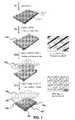
- FIG. 1Schematic summarizing processing steps for creating microstructures of thin film ultrananocrystalline diamond and for transferring these elements from a growth substrate to a target substrate using a printing technique.
- FIG. 2Optical microscope images and scanning electron microscope images (inset) of transfer-printed UNCD microstructures. a) Isolated ribbons on glass. b) I-shaped structures on glass. c) Membrane printed on glass. d) Isolated ribbons on GaAs. e) Isolated ribbons on Si. f) Photo of ribbons on PET, in a bent configuration.
- FIG. 3‘Wavy’ diamond ribbons on a rubber substrate.
- a)Optical microscope top-view images of wavy diamond ribbons on PDMS.
- c)Optical images of wavy diamond ribbons on PDMS under different applied strains: ⁇ 5.1%, ⁇ 3.1%, ⁇ 1.0%, 3.1%, and 5.1% from the unperturbed state, evaluated along the lengths of the ribbons.
- FIG. 4Optical microscope images of serpentine microheaters on plastic substrates collected at applied powers of 53 mW, 97 mW, and 160 mW, for the case of heaters (a) exposed to air, (b) coated with a thin (600 nm), spin cast layer of PMMA and (c) covered with a printed, thin (400 nm) platelet of diamond. d) Average heater temperatures from experiment and from finite element modeling as a function of applied power for these three different samples.
- FIG. 5Infrared images of microheaters on PET at various applied powers. a) Au microheater on PET film at 97 mW and 160 mW. b) Au microheater with PMMA top layer at 97 mW and 160 mW. c) Diamond membranes-printed Au microheater at 97 mW and 160 mW. d,e,f) Temperature profiles in cross-section from finite element analysis at 97 mW and 160 mW.
- FIG. 6RF semiconductor electronic device platform.
- FIG. 7Thermal simulations for: printed GaN chiplets and: A. Diamond heat spreaders; B. Diamond heat spreaders and dummy CMOS die; C. Dummy CMOS die.
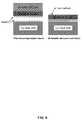
- FIG. 8Diamond on copper substrate preparation.
- FIG. 9Schematic illustration of the assembly process step.
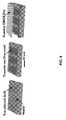
- FIG. 10Micrographs of GaN printed on Si Wafer (left panel) and Diamond printed on glass substrate (right panel).
- FIG. 11Histogram of placement accuracy of a micro-stamping tool capable of high-fidelity and placement accuracy for transfer of large-area semiconductor elements from donor wafers to target substrates.
- FIG. 12Cross-sectional schematics of (A) state of the art GaN on SopSiC and (B) semiconductor platform utilizing diamond for thermal management.
- FIG. 13Structures fabricated to isolate and test the relative effect of printing a thermal diamond overlayer on the devices. The devices are equivalent except that the right panel incorporates a diamond heat spreader.
- FIG. 14Schematic cross-sections of the devices tested.
- IA and IBhave structures fabricated on a silicon substrate without and with a thin diamond thermal spreader printed on top of the devices, respectively.
- IIA and IIBconsist of structures fabricated on a 50 micron diamond film deposited onto a thick silicon substrate, again without and with a diamond spreader printed on top of the devices, respectively.
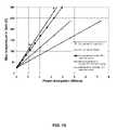
- FIG. 15Plot of junction temperature (in GaN layer) as a function of power dissipation for various substrates with the addition of a diamond overlayer on the NiCr resistive heater.
- Heat-sinkedrefers to a passive, active or both passive and active element that facilitates heat transfer from a heat-generating component, such as an electronic component, to either a part of the component that is not sensitive to high temperature or to the surrounding medium (e.g., air).
- a “heat sink”refers to an element capable of receiving a significant amount of heat without a significant increase in temperature in a heat-sensitive device or component. Examples include relatively large volumes of good heat conductors, such as copper or other metals, for example.
- a heat sinkmay also refer to ambient air surrounding a heat radiating-element, such as patterned microstructures disclosed herein that may be shaped into arrays of heat-radiating fins, for example. The exact composition of the material is not important, so long as the heat sink is capable of removing heat from the heat-sensitive electronic component, thereby effectively decreasing the operating temperature of the electronic component.
- Transistors, diodes, and capacitorsare examples of electrical or “electronic components” that may be combined with the thermal management processes provided herein to yield improved temperature regulation and/or isolation.
- an electronic componentmay itself be a device, such as a solar cell, array of transistors, integrated circuits, flexible fabrics or displays or any other relatively complex combination of electronic components.
- the componentmay be, without limitation, a passive or active circuit element, or an integrated circuit chip.
- Diamondis used broadly to refer to natural and synthetic diamond such as polycrystalline diamond including ultrananocrystalline diamond made by methods known in the art, such as by chemical vapor deposition (CVD) (see, e.g., U.S. Pat. No. 5,907,189) or plasma jet deposition systems (see, e.g., U.S. Pat. Nos. 5,648,148, 4,471,003, 4,487,162 and 5,204,144). Other methods may be used as desired, so long as a layer of diamond is deposited on a substrate, such as a layer that is less than about 1 ⁇ m thick.
- CVDchemical vapor deposition
- plasma jet deposition systemssee, e.g., U.S. Pat. Nos. 5,648,148, 4,471,003, 4,487,162 and 5,204,144.
- Other methodsmay be used as desired, so long as a layer of diamond is deposited on a substrate, such as a layer that is less than about 1 ⁇ m thick.
- Nanocrystallinerefers to a diamond having nanoscale grain sizes
- “ultrananocrystalline”refers to grain sizes on the order of between about 1 and 10 nm, or between about 3 and 5 nm, for example.
- thermal conductivitye.g., relatively low or relatively high
- Other properties of the diamondsuch as the surface roughness and stress of the film, may be optimized at the expense of the thermal conductivity of the films in order to facilitate transfer printing and integration with other materials.
- dielectric propertiese.g., relative dielectric constant, dielectric strength, loss tangent at high frequencies are optimized as desired for a given device operation frequency range.
- Patternrefers to a spatial variation in a material, such as the depth or thickness of a material that varies over a surface. “Pattern” may also refer to a parameter of a material that varies over a surface. A specific diamond pattern is selected depending on the application for which the diamond is used. “Micropattern” refers to one or more structures having at least one dimension on the micrometer scale, such as less than 1000 ⁇ m, 100 ⁇ m, 10 ⁇ m, or a dimension that is selected from a range of 100 nm to 100 ⁇ m, or any range therein as desired. In particular, a micropattern can have a spatially-varying pattern of elements, such as strategic placement of one or more heat-conducting or wear-resistant elements such as diamond.
- micropatternrefers to a situation where the height or depth of a single structure varies over at least a portion of the surface location of the substrate to which the micropattern thermally contacts.
- the diamondis of any thickness, as desired, depending on operating conditions, parameters and heat generation, for example.
- the diamondhas a thickness that is thin, such as less than 100 ⁇ m, less than 10 ⁇ m, less than 1 ⁇ m or less than 500 nm.
- “Feature”is used broadly to refer to a diamond element in thermal contact with a device, device component or substrate region to provide thermal dissipation.
- Such a featuremay be free-standing on a surface, or alternatively may itself be connected to other elements, conduits or other diamond features for additional physical support or thermal dissipation.
- Particularly useful featuresinclude those that are shaped to maximize heat exchange such as fins or heat radiators.
- Other featuresare selected to take advantage of a desired diamond property, such as diamond's relative hardness, wear resistance, physical characteristics (e.g., modulus) or index of refraction.
- the particular pattern or micropatternis selected so that any one or more of these characteristics provide the desired “performance characteristic” to a device. For example, where the desired performance characteristic is to increase the hardness of a device, diamond may be printed to coat regions of the device where increased hardness is desired. Similar patterned diamond printing is performed to provide a performance characteristic related to an optical property, mechanical property, flexibility, thermal dissipation, or other diamond-based parameters of interest.
- a “pattern of bond sites”refers to spatial application of bonding means to a supporting substrate surface and/or to the diamond so that a supported diamond has bond regions and non-bond regions with the substrate.
- a diamond ribbonthat is bonded to the substrate at its ends and not bonded in a central portion. Further shape control is possible by providing an additional bond site within a central portion, so that the not-bonded region is divided into two distinct central portions.
- Bonding meanscan include adhesives, adhesive precursors, welds, photolithography, photocurable polymer.
- bond sitescan be patterned by a variety of techniques, and may be described in terms of surface-activated (W act ) areas capable of providing strong adhesive forces between substrate and feature (e.g., interconnect) and surface-inactive (W in ) where the adhesive forces are relatively weak.
- W actsurface-activated
- W insurface-inactive
- a substrate that is adhesively patterned in linesmay be described in terms of W act and W in dimensions.
- Thermal contactrefers to the ability of two materials that are capable of substantial heat transfer from the higher temperature material to the lower temperature material, such as by conduction. Bent structures resting on a substrate are of particular use in providing regions that are in thermal contact (e.g., bond regions) with the substrate and other regions that are not in thermal contact (e.g., regions that are insulated and/or physically separated from the substrate). Thermal contact refers to two elements that are in physical contact with each other. Alternatively, thermal contact refers to two materials that are not in direct physical contact with each other, but instead may be separated by another material (e.g., air, adhesive coating, etc.). The term is used broadly to refer to the functionality such that the material can dissipate heat build-up, with an end result of decreasing or substantially abolishing the temperature increase that would otherwise occur.
- “Buckled”refers to micropattern that has a separation distance from the substrate to which the micropattern is thermally connected that varies.
- ribbons of diamondwhose separation from the substrate varies along the length of the ribbon.
- Such a geometrycan be described as buckled or “wavy.”
- that geometrycan be obtained by exerting a force (e.g., a strain) on diamond by exerting a force on an underlying deformable substrate (e.g., stamp surface used to transfer the diamond micropattern), such that a change in a dimension of the underlying substrate generates buckles or waves in the diamond.
- an individual diamond ribbonmay be defined by portions that are bonded to a target substrate, and a curved central portion between the ends that does not physically contact the substrate (e.g., are not bonded to the substrate).
- “Curved” or “buckled”refers to relatively complex shapes, such as by a diamond pattern having one or more additional bond regions in the central portion.
- “Arc-shaped”refers to a generally sinusoidal shape having an amplitude, where the amplitude corresponds to the maximum separation distance between the diamond micropattern and the substrate surface.
- “Flexible”refers to a material that is capable of undergoing strain, such as bending or stretching, without adverse impact of physical characteristics, such as irreversible break-down associated with material fracture, for example. “Stretchable” is used in a similar manner to refer to reversible strain without material fracture.
- Axial strainrefers to a force applied to an axis of the substrate to generate the displacement ⁇ L. Strain is also generated by forces applied in other directions, such as a bending force, a compressive force, a shearing force, and any combination thereof. Strain or compression may also be generated by stretching a curved surface to a flat surface, or vice versa.
- Level of strainrefers to the magnitude of the strain and can range from negative (corresponding to compression) to zero (relaxed state) to positive (corresponding to elongation or stretching).
- Young's modulusis a mechanical property of a material, device or layer which refers to the ratio of stress to strain for a given substance. Young's modulus may be provided by the expression;
- EYoung's modulus
- L 0the equilibrium length
- ⁇ Lthe length change under the applied stress
- Fthe force applied
- Athe area over which the force is applied.
- Young's modulusmay also be expressed in terms of Lame constants via the equation:
- ⁇ and ⁇are Lame constants.
- High Young's modulusor “high modulus”
- low Young's modulusor “low modulus” are relative descriptors of the magnitude of Young's modulus in a give material, layer or device. Compression is used herein in a manner similar to the strain, but specifically refers to a force that acts to decrease a characteristic length, or a volume, of a substrate, such that ⁇ L ⁇ 0.
- Contact printing methods for assembling, organizing and/or integrating printable elements, such as diamond patterns, in the present methodsinclude dry transfer contact printing, microcontact or nanocontact printing, microtransfer or nanotransfer printing and self assembly assisted printing, as known in the art.
- Various patents, patent applications and publicationsare hereby incorporated by reference for various transfer methods, stamps, printing, and related materials, processes and devices, including “Pattern transfer printing by kinetic control of adhesion to an elastomeric stamp” Ser. No. 11/423,192 (41-06 filed Jun. 9, 2006).
- “Registered transfer”refers to a substantially one-to-one transfer of elements from one substrate surface to a second surface, such as from a donating to a receiving surface.
- a “bridge”may be etched in the patterned diamond to facilitate controlled breakage and lift-off of the diamond structure. Examples of such a bridge are illustrated by the tethers and anchors in FIG. 1 that connect to-be-transferred diamond elements with diamond regions that have not been undercut etched. Other bridge geometries are provided as needed depending on the geometry of the diamond elements to-be-printed.
- Thin film diamondhas many potential applications in electronics[1] and optoelectronics,[2,3] microelectromechanical systems (MEMS),[4,5] wear resistant coatings[6], thermal management[7] and other areas, due to its exceptional electronic, optical, mechanical, chemical/tribological and thermal properties, respectively.
- Diamondis most commonly implemented in these systems by directly growing the material on the surfaces of device substrates, where it is used as uniform or lithographically patterned films. This approach places restrictions on the range of applications because known growth techniques involve high temperatures, vacuum or low pressure conditions and often other demanding conditions.[12,13] Implementing thin film diamond on low temperature plastics, for example, is not possible.
- FIG. 1shows the main processing steps for forming and printing micropattern of diamond 100 comprising, in this example, microstructures 105 of thin films of UNCD, referred to as ⁇ s-UNCD.
- chemical vapor deposition with methane as a carbon source[14, 15]forms a uniform film (400 nm thick) of UNCD on a SiO 2 (1 ⁇ m)/Si substrate. This process, which involves continuous renucleation during growth, leads to films with nanoscale grain sizes (3 ⁇ 5 nm) and other interesting properties.[15, 16]
- PECVDplasma enhanced chemical vapor deposition
- Photolithography and reactive ion etching (RIE) with a CF 4 plasmadefines a pattern in this SiO 2 layer.
- RIE with an O 2 plasmaremoves both the photoresist and the exposed UNCD.
- the SiO 2 on top of and beneath the patterned UNCDis then removed with concentrated hydrofluoric acid (HF 49%).
- HF 49%)concentrated hydrofluoric acid
- controlled etchingallows the UNCD structures to be undercut completely, but in a manner that keeps them tethered to the substrate to prevent their removal into the etching bath.
- these tethers, or ‘anchors’ 110consist of narrow regions at the ends of ribbons of UNCD.
- the printing stepinvolves first contacting a substrate processed in this manner with a slab of an elastomer (i.e. the stamp 130 ), to establish a conformal wetting contact with the top surface of the ⁇ s-UNCD through the action of van der Waals forces.[17] Peeling the stamp away from the substrate at a high rate leads to the selective fracture of the UNCD structures at points of stress concentrations that form at the anchors,[18] thereby removing these structures from their growth substrate.
- the stampinked with ⁇ s-UNCD in this manner, then delivers these elements to a target substrate 120 , such as plastic, glass, rubber or a semiconductor wafer, in a room temperature process that involves contact and then peel back of the stamp at a slow rate.
- Substrate 120has a top surface 150 and a bottom surface 160 .
- the micropattern of diamondis bonded to bottom surface 160 and an electronic component is connected to the top surface 150 .
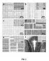
- FIG. 2shows scanning electron and optical microscope images of diverse classes of thin (400 nm in this example) diamond microstructures, including membranes ( FIG. 2 c ; square array of 3 ⁇ m diameter holes separated by 40 ⁇ m to enable SiO 2 undercut etching) interconnected meshes ( FIG. 2 b ; I-shapes with widths and lengths of 25 and 100 ⁇ m) and arrays of isolated ribbons ( FIGS. 2 a, d, e and f ; widths and lengths of 10 and 175 ⁇ m, respectively), printed with poly(dimethylsiloxane) stamps (PDMS; Dow Corning) onto various substrates, including glass ( FIGS. 2 a, b, c ), GaAs ( FIG.
- PDMSpoly(dimethylsiloxane) stamps
- FIG. 2 dsilicon
- FIG. 2 esilicon
- plasticpolyethyleneterephtalate, PET, with 100 ⁇ m thickness
- FIG. 2 fplastic
- a thin, spin-cast layer⁇ 1.0 ⁇ m
- benzocyclobuteneBCB, CYCLOTENE 3022-35 Resin, Dow Chemical
- Adhesiveless printingwas used for GaAs, silicon and PET, in which the transfers were facilitated by (i) the large differences in surface energies of the target substrates (43 mJ/m 2 for PET, 1140 mJ/m 2 for Si, 860 mJ/m 2 for GaAs and 19.8 mJ/m 2 for the PDMS),[19,20] (ii) viscoelastic effects associated with low rates for peeling back the stamps,[21] (iii) the low roughness on the bottom surfaces of the ⁇ s-UNCD elements (root-mean-squared (rms) roughness of ⁇ 1.8 nm, as measured by atomic force microscopy with a standard tip) and the receiving substrates (rms: 0.22 nm for Si, 0.25 nm for GaAs, 0.45 nm for glass and 38 nm for PET), and (iii) shear forces to facilitate crack formation at the PDMS/UNCD interface.
- the target substrates43 m
- the topsides of the UNCD structuresexhibit the nanometer-scale roughness characteristic of UNCD, while the undersides are smooth.[22]
- the high printing yields (85%>in all cases) and the uniformity of the fracture points associated with the isolated ribbons ( FIGS. 2 a, d and e )are evidence of well controlled, repeatable processes.
- the results of FIG. 2 findicate the ability to bend, without cracking, the ⁇ s-UNCD when placed on a thin plastic sheet.
- the small thicknesses of both the substrate and the ⁇ s-UNCDlead to small strains at the surface for moderately small bend radii.
- the strain, ⁇ , in the diamondis approximately equal to:
- E P and h P , and E D and h Dare modulus and thickness of PET substrate and diamond, respectively;
- ris the bending radius.
- Structural configurations that combine thin, flexible geometries such as these with ‘wavy’ shapescan impart mechanical stretchability to these elements, in strategies that are conceptually similar to those recently described for single crystalline elements of Si, GaAs and other materials.[23,24] (see also U.S. patent application Ser. No. 11/851,182, filed Sep.
- FIGS. 3 a and bshow optical and scanning electron microscope images of arrays of substantially parallel ribbons 180 that are buckled or wavy UNCD, created by transfer printing these elements onto a prestrained ( ⁇ 4.8% created by heating to 180° C.) substrate of PDMS followed by release of this prestrain.[25]
- the distances between the ribbons in this caseare sufficiently small that mechanical coupling results in phase coherent buckling patterns.
- the waveshave uniform, periodic structures with wavelengths of 85.2, and 86.3 ⁇ m for prestrains of 4.8 and 3.9%, respectively.
- the prestrain dependent wavelength valuesagree well with other experimental observations and accurate models of the mechanics.[23,26] FIG.
- 3 cpresents optical images of stretchable diamond ribbons (the sample prepared with 4.78% prestrain) with various levels of strain at compressed, unperturbed, and stretched states. For applied compressive strains larger than ⁇ 5%, some cracking of the UNCD was observed ( FIG. 3 c ).
- the PET substrate( ⁇ 75 ⁇ m) could be easily damaged by heat generated by the microheater.
- the first stage of thermal degradationoccurred at temperatures close to the melting point of 260° C., followed by a second stage characterized by weight loss at around 350° C.[28,29]
- the imagesshow that the sample with ⁇ s-UNCD exhibits the most robust behavior to heating, indicating its effectiveness in heat spreading.
- FIG. 4 dpresents the average temperature of the microheaters for the three different cases, as a function of applied power.
- the temperatureswere computed from the known temperature dependence of the resistivity of the metal microheater, according to:
- R ( T )R a [1 +TCR a ( T ⁇ T a )],
- R a and TCR aare the resistance and temperature coefficient of resistance, respectively, evaluated at temperature T a .
- the resistance R ais determined by:
- ⁇ aresistivity of gold at T a
- Lis length
- Ais cross-sectional area of gold wire.
- the value of R(T) valueis obtained simply by dividing applied voltage (V) by the current (I).
- ⁇ (20° C.) and TCR(20° C.) for goldare 2.214 ⁇ 10 ⁇ 8 ⁇ m and 0.003715/° C. at 20° C.
- Taverage temperatures at various applied voltages and currents.[30-32]
- the temperatures of the microheater, PMMA/heater, and ⁇ s-UNCD/heater systemswere, respectively, 261° C., 257° C., and 208° C. at a power of 97 mW, and 350° C., 329° C., and 279° C. at a power of 160 mW.
- FIGS. 5 a, b and ccorrespond to the uncoated, the PMMA and the ⁇ s-UNCD cases, respectively, for applied powers of 97 mW and 160 mW.
- the temperature distribution of the ⁇ s-UNCD samplehas a rectangular shape with a broad thermal distribution, while the uncoated and PMMA-coated cases show localized heating distributions centered on the gold wires. These distributions illustrate that the UNCD platelet efficiently spreads heat laterally and thereby reduces the peak temperatures. Simple finite element analysis of the heat flow was conducted to reveal further this behavior.
- 2D analysisyields expected temperature distributions for the three systems at different applied powers.
- the simulated cross-sectional temperature profilesare shown in FIG. 5 d - f .
- the gold heater elementssupply heat to the system (via Joule heating) which then exits via conduction through the 75 ⁇ m PET substrate below the heater and through the PMMA or ms-UNCD coatings and then through a 40 ⁇ m of air (i.e. ‘dead air’) above the structure.
- the width of the modeled systemis ⁇ 1 mm.
- etching and printing procedurescan be used to manipulate thin film microstructures of diamond in a manner that permits integration with substrates (e.g. plastic) and creation of structural forms (e.g. bent or wavy) that are incompatible with conventional processing.
- substratese.g. plastic
- structural formse.g. bent or wavy
- the resulting capabilitiesare useful for certain applications, such as those in thermal management for plastic electronics.
- a SiO 2 layer(300 nm thick) was deposited by plasma-enhanced chemical vapor deposition (PECVD) using SiH 4 and N 2 O at 250° C.
- PECVDplasma-enhanced chemical vapor deposition
- Photolithography with AZ 5214defined a pattern of photoresist (PR) on the surface of the SiO 2 (300 nm)/UNCD (400 nm)/SiO 2 (1 ⁇ m)/Si substrate.
- the PRserved as a mask for RIE etching of the PECVD SiO 2 layer with a CF 4 plasma (Plasmatherm RIE system, 40 sccm CF 4 flow with a chamber base pressure of 50 mTorr, 100 W RF power for 15 min 30 sec).
- the exposed regions of the UNCDwere then etched with an O 2 plasma (chamber pressure of 40 mTorr, 20 sccm O 2 flow, and 220 W RF power for 35 min).
- O 2 plasmachamber pressure of 40 mTorr, 20 sccm O 2 flow, and 220 W RF power for 35 min.
- more efficient use of the diamond source wafer and reduction in processing timeis achieved by the use of heterogeneous and/or homogeneous anchor structures, as provided in U.S.
- Stamps of poly(dimethylsiloxane)were formed by casting and curing in polystyrene Petri dishes, and then cutting to convenient dimensions. Laminating such stamps against processed ⁇ s-UNCD substrates and then quickly peeling them back lifted the ⁇ s-UNCD onto the surface of the stamp. Contacting these ‘inked’ stamps against a receiving substrate and then slowly peeling them back transferred the ⁇ s-UNCD to the receiver. In certain cases, this transfer was facilitated either by the application of a small shear force to the stamp while in contact with the receiver or by use of a separate adhesion layer.
- PDMSpoly(dimethylsiloxane)
- Preparation of wavy diamond ribbonsAfter creating ⁇ s-UNCD ribbons according to the process of FIG. 1 , thin layers of Cr (3 nm thick) and SiO 2 (30 nm thick) were deposited by electron beam evaporation (Temescal, Inc). We found that the Cr enhanced the adhesion between the ⁇ s-UNCD and SiO 2 .
- a flat sheet of PDMS( ⁇ 3 mm thick) was exposed to ultraviolet light in air to create a hydrophilic surface (—OH and —O—Si—O— end groups),[24] that can provide the strong bonding with the SiO 2 /Cr coated ⁇ s-UNCD. Heating the surface modified PDMS substrate in a convection oven generated prestrain by thermal expansion.
- the coefficients of thermal expansion, ⁇are 3.1 ⁇ 10 ⁇ 4 K ⁇ 1 and 1.2 ⁇ 10 ⁇ 6 K ⁇ 1 for PDMS substrate and UNDC, respectively.
- the thermally induced prestrain, ⁇ prefor samples heated to 180° C. was calculated by:
- the prestrained PDMSwas brought into conformal contact with the ⁇ s-UNCD ribbons, and then peeled back to leave the ribbons adhered to the PDMS. Subsequent heating in a convection oven led to strong adhesion between ribbons and the PDMS. Finally, the sample was cooled to room temperature (25° C.) to release the thermally induced prestrain, thereby creating the wavy ⁇ s-UNCD via a nonlinear buckling process.
- Photolithography with AZ nLOF 2020 for negative imagingdefined a pattern of resist on a sheet of PET (75 ⁇ m thick). A uniform bilayer of Ti(3 nm)/Au(300 nm) was then deposited by electron beam evaporation (Temescal, Inc.). Removal of the photoresist by acetone followed by washing with water completed the fabrication of the microheaters. A thin (300 nm), spin-cast layer of BCB was used to planarize the heater structure, and then the ⁇ s-UNCD platelets were printed on top. After printing, the samples were placed on a hot plate at 100° C. for 10 min, and then in an oven at 75° C. for 24 h to cure the BCB.
- PMMA A6(Microchem corp.) was spin-coated on top of Au microheater at 2000 rpm for 45 s to produce PMMA layer of 600 nm thickness, and placed in an oven at 75° C. for 8 h for removing solvent.
- Semiconductor printing technologyfacilitates heterogeneous integration onto of state of the art RF power devices.
- This integration platformcan dramatically improve overall thermal dissipation and optimize heat dissipation paths to prevent thermal-cross talk between power and control circuits.
- the critical noveltyresides in the fact that it permits the ultra-fine heterogeneous integration of RF power devices and CMOS control circuits with high performance heat spreaders onto thermally engineered substrates.
- the assembled substratewill circumvent thermal cross-talk issues by combining passive and active substrate materials (insulators and semiconductors) on a 5-20 micron length scale as a heterogeneous assembly, providing integrated thermal management, not just isotropic thermal dissipation.
- the end goal system structureenables the design of high efficiency power amplifiers tightly controlled by a CMOS circuit through short range interconnects with greatly reduced thermal feed-through to the control circuit.
- the RF semiconductor electronic device platformcombines devices of different materials into a single small-scale microsystem enabling superior functionality to separate individual semiconductor devices.
- This platformis heterogeneously assembled of semiconductor devices through a precise and scalable device transfer process.
- Combining semiconductor technologies at a device-by-device scalepermits achievement new electronic functionalities, for instance: integrating sense and modulate intelligence with highest efficiency RF power devices.
- the resulting RF microsystemhas reduced thermal energy loss (1/PAE) and related loss of device functionality (frequency-power-linearity) at RF frequencies, particularly microwave and mm-wave. Thermal energy is managed more efficiently by designing highly conductive thermal pathways, not just thermal dissipation into the assembled substrate.
- RF semiconductor electronic device platformTo test this approach, we construct a heat-sinked electronic component 200 in an assembled substrate comprising a highly thermally conductive diamond pattern 100 connected to a heat sink 170 comprising a copper substrate, GaN chiplets, diamond heat spreaders, and a CMOS die (see FIG. 6 ). This assembled device platform provides superior thermal management, which can be verified through both modeling and experiment.
- the semiconductor device platformexhibits dramatically improved overall thermal dissipation (>30% improvement compared to GaN on SiC). Furthermore, optimization of thermal dissipation paths prevents or substantially hinders thermal-cross talk between power and control circuits (targeting>1000:1 heat flux ratio).
- Some key technical challenges in developing the semiconductor device platformare: Selective dry-transfer onto GaN chiplets onto diamond on copper substrates; Release of the diamond thin film to allow dry-transfer; Selective dry-transfer of diamond heat spreaders above GaN chiplets to create highly tailored thermal pathways; Controlling interfaces to minimize thermal resistance.
- Thermal simulationsIn order to estimate the overall thermal dissipation characteristics of the proposed semiconductor device platform, thermal simulations are conducted for three cases outlined in FIG. 7 A) Printed GaN chiplets+Diamond heat spreaders; B) Printed GaN chiplets+Diamond heat spreaders+dummy CMOS die; C) Printed GaN chiplets+dummy CMOS die.
- the underlying copper heat sink substrateis assumed to be an infinite perfect thermal conductor as the main purpose of these preliminary simulations is to compare the above listed three cases.
- These simulationsshow that the proposed semiconductor electronic device platform can efficiently manage thermal heat flux toward the copper heat sink substrate and minimize thermal feed-through to the control CMOS circuit (with heat flux ratio potentially greater than 2,000:1).
- These simulation resultsalso indicate that printing a 2 micron thick diamond heat spreader onto the GaN chiplets can induce a ⁇ 11% decrease of the GaN device junction temperature.
- RF semiconductor electronic device platform manufacturing processbegins with deposition of a ⁇ 50 micron thick diamond coating on a polished silicon wafer. By adjusting the process conditions during growth as well as employing wafer-level stress management, 50 micron thick films can be made with residual stresses that are low-enough to meet wafer bow specifications necessary for bonding at the wafer level and for lithography.
- Diamondis optionally attached to a copper substrate using a solder (e.g., indium-silver) die attach process.
- a thin film metallic adhesion promotion layeris optionally deposited (such as by sputtering) onto the surface of the diamond film in order to increase the strength of die attachment to the diamond film.
- Such processesprovide diamond film bonding, using thermo-compression eutectic bonding, onto a polished copper substrate (see FIG. 9 ).
- This bonding processis performed at moderate temperatures ( ⁇ 300° C.) and pressures ( ⁇ 10 6 Pa) using a standard die bonder.
- the diamond filmis etched into isolated small islands prior to performing the die bonding process using oxygen reactive ion etching and a simple shadow mask for patterning.
- Thick diamondis optionally etched into isolated islands using a relatively slow plasma etching process.
- Thick diamondis optionally etched using a laser dicing process.
- the temporary silicon carrieris then dissolved by wet etching in order to leave on the top surface an ultra flat diamond ( ⁇ 1 nm rms) surface onto which GaN chiplets are transfer printed.
- Heat spreadersconsisting diamond films that are 2 micron thin and grown under conditions to minimize the differential stress in the films, are then transferred onto the GaN chiplets in order to enable efficient heat extraction from the top surface of the GaN chiplets.
- a silicon die populated with thermally sensitive elementsis stacked onto the assembled structure. The inter-substrate spacing is controlled by use of ⁇ 10 ⁇ m tall spacers.
- FIG. 10schematically illustrates an assembly process.
- Resistive heatersare fabricated on the surface of the GaN chiplets in order to simulate the heat required to be dissipated by power HEMTs devices. Power applied to the heaters is cycled in order to evaluate the robustness of the printed material stack. Heat flux to the heat sink substrate and surface temperature of a dummy CMOS die is measured to verify experimentally the heat extraction performance of the proposed structure.
- This technologyprovides a platform for integrating state of the art GaN HEMTs on to thermally engineered substrates to enable efficient heat extraction. Dry transfer printing process permits the heterogeneous integration of materials on the device scale of 5-25 microns at significantly higher resolution than that of existing interposer or pick-and-place heterogeneous assembly technologies (see, e.g., Ser. Nos.
- a possible area of riskrelates to materials CTE mismatch during diamond bonding onto Cu heat sink. This is mitigated by one or more of: reducing area of transfer; pattern diamond layer into isolated islands; etch isolation trenches in Cu heat sink; use of a lower melting point eutectic.
- Another concernrelates to appropriate bonding of the GaN chiplets onto the diamond layer. This concern is alleviated by: use of an ultra thin glue layer stable at ⁇ 250° C.; use of metal eutectic bonding pads in the chiplet peripheral area and/or in direct contact with the underlying diamond layer.
- FIG. 11Examples of placement accuracy for various patterns from a donor substrate to a target substrate are provided in FIG. 11 .
- the printing platformprovides for micron and sub-micron placement accuracy.
- Integration technology achieved via transfer printingcan significantly improve overall heat extraction from heat-generating devices, such as from the active junction of GaN high power devices.
- Exemplary components of such heat-extraction devicesinclude, copper/diamond heat sink substrate, GaN chiplets transfer printed on the heat sink substrate, and thin diamond heat spreaders transfer printed and incorporated into the device.
- the performance of the semiconductor device platformsare evaluated and compared to conventional state of the art semiconductor platforms.
- FIG. 12AA state of the art GaN on SopSiC is illustrated in FIG. 12A .
- FIG. 12BA corresponding semiconductor platform incorporating the processes and systems provided herein for improved heat extraction is illustrated in FIG. 12B .
- the performance of the semiconductor device platform proposed in FIG. 12Bis compared against state of the art GaN devices fabricated on Silicon on poly-crystalline Silicon Carbide (SopSiC) substrates ( FIG. 12A ).
- FIG. 12Balso illustrates that incorporation of a diamond material can provide multiple functional benefits to a device, in this case a heat-sinked high-powered RF device (e.g., GaN device) 300 .
- a diamond layer 310provides electrical insulation between device 300 and a conductive substrate 320 (e.g., Cu).
- the diamond layer 310has a different position and geometry (e.g., thickness) than another diamond layer that faces the opposite surface of the GaN device (compare 50 ⁇ m and 2 ⁇ m).
- Configuration and printing of diamond layers and patternsmay be selected based on the main purpose of the layer, such as thermal dissipation, electrical isolation or dielectric loss.
- the diamond layerhas a low dielectric loss so that the diamond material does drain energy away from the device, thereby further improving performance.
- Incorporation of diamond layers to achieve desired level of electrical isolation at desired device radiofrequency (RF) rangese.g., MHz to THz, with the precise range depending on the specific device characteristics
- RFradiofrequency
- Further information related to low loss tangent at different frequenciesis provided in Garin et al. (Nature of millimeter wave losses in low loss CVD diamonds. Diamond and Related Materials. 12 (10-11), 2003: 1755-1759. Proceedings of the 8th International Conference on New Diamond Science and Technology (ICNDST-8)).
- Heat Sink Substrate PreparationGrowth of 50 ⁇ m thick diamond on Si wafer.
- two types of 50 ⁇ m thick films1) 50 ⁇ m films deposited onto 50 mm diameter thick (1 ⁇ 8′′) silicon disks (2), and 2) Twelve 50 ⁇ m thick films deposited onto 700 ⁇ m and 3 mm 1 ⁇ 1 cm silicon coupons, for bonding work.
- the chemistry to synthesize these filmsis optimized to produce the highest thermal conductivity diamond, which leads to the formation of films with a highly columnar grain structure with grain sizes at the as-grown surface up to 100 ⁇ m in size.
- the films for process developmentis polished down to ⁇ 5 nm rms roughness, so that chiplets can be transferred directly to this surface. These films on thick silicon substrates are subsequently used for the final devices tested.
- Thin Diamond Capping Heat SpreaderA wafer with about 2 ⁇ m thick UNCD Aqua100 is used to make the final device.
- Delineation of diamond heat spreadersThe same mask and microfabrication processes is used to pattern and fabricate the heat spreaders as described herein.
- Wafers having 2 um thick diamond films grown on 100 mm silicon wafersare optimized to have material properties most similar to bulk diamond, including the high thermal conductivity. Although patterning and printing micro-stripes of these films onto flat surfaces is relatively straightforward, printing onto more complex 3D substrates is challenging and requires heater and chiplet geometries to make the surfaces as planar as possible. Using the alternative design the yield of the transfer printing process is greatly improved and several devices are constructed for further testing. The final structures fabricated for further testing are shown in FIG. 13 .
- the diamond filmsare also very transparent in the IR, facilitating the direct measurement of the heater temperatures as discussed below.
- Device test and simulationsTemperature and heat flux measurements. Thermal imaging tests of the final as-fabricated heterostructures are conducted using a QFI Infrascope II. For each device tested the base plate is maintained at a constant temperature (50 or 60 C) and the temperature of the devices imaged while current is run passed through the integrated heaters with input powers ranging from about ⁇ 0.2 to 8.5 watts of power. The lateral resolution of the thermal imaging is sufficient to determine the temperature along the heater lines (thin film electrode) and in the immediate regions surrounding the lines quite easily. Overall, more than 300 devices are evaluated. Direct determination of the temperatures precisely on the lines of the heaters is made possible by the low IR adsorption of the diamond films, which is a secondary confirmation of the quality of the films.
- FIG. 14Two types of structures are tested and yielded meaningful results from which to draw conclusions in comparison to the thermal simulations. These structures are shown in FIG. 14 .
- a film grown onto a thick (1 ⁇ 8 inch) silicon substrateis used.
- the surfaceis polished to ⁇ 5 nm rms roughness.
- GaN chipletsare not used due to the high differential stresses in the nitride layers, leading to non-planar contacts after transfer printing them to the diamond and silicon substrates. Strategies are available to minimize this problem to accommodate GaN chiplet printing. To expedite progress on demonstrating key concepts, data presented in this example are for pure silicon chiplets.
- Structure IThese specimens consisted of a standard silicon substrate (about 500 microns thickness) on which silicon chiplets with micron-strip heaters are printed. A SiN passivation layer is deposited on top of the chiplets prior to printing (for electrical isolation). Some of the structures (IA) are tested in this configuration while others (IB) have thin film (2 micron thick) diamond heat spreaders transfer printed on top of them in a second transfer process (see top panel of FIG. 14 ). Prior to doing this an ultra thin ( ⁇ 30 nm) layer of BCB is coated on top of the SiN layer to promote adhesion of the diamond heat spreader to the silicon chiplet.
- Structure IIconsisted of the same structures that were discussed above (Structure 1) but transfer printed onto a substrate consisting of the 50 micron thick polished diamond film on a thick silicon substrate. Again, some of the devices tested have diamond heater spreaders transfer printed on top of them (IIB) and others do not (IIA), allowing for the addition performance benefit of the thin diamond to be evaluated.
- Table Isummarizes their relative performance for input powers close to 3W only.
- Thermal imaging dataare obtained for these devices with the performance characteristics as summarized in Table 1. From these data and images and other work described herein, several conclusions can be drawn: (1) Transfer printing can be used to integrate these devices with both thick and thin diamond thermal materials to enhance their ability to perform at higher powers and lower operating temperatures; (2) The reduction of the max temperatures on the heater lines is significant, with the diamond substrate and overlayer lowering the temperature by a maximum of 84% and 10%, respectively; (3) Based on the model, we estimate that this integration pathway could be used to increase the power handling capability from about 15 W/cm to about 40 W/cm, based on a maximum allowable junction temperature of 150° C. If the junction can operate continuously at 250° C.
- Table IIprovides the W/mm observed at a GaN junction temperature of 200° C. and percent differences observed by varying the substrate and package (sub-mount). It is shown that the use of a thin diamond overlay results in an observed improvement of ⁇ 13%. The combined used of this thin diamond overlay with a 50 um thick diamond substrate results in an observed improvement of 74%, and ultimately up to 172% if the sub-mount is also made out of diamond.
- Thermal conductivities of the diamond overlayer and substratewere 1000 and 1350 W/m ⁇ K, respectively, which are conservative values. Also, only constant thermal conductivity values were considered in this version of the model where in reality the thermal conductivity is known to vary with temperature. 2. Limited physical information was available on the material used for the experimental study, so all thermal properties were assumed to be isotropic in this thermal model. 3. Perfect array symmetry (thermal insulation) lateral boundary conditions were used on the outside edges of the device model. This assumption is valid for the case of power devices assembled in a densely packed array configuration (applications such as millimeter-wave arrays). However, this assumption does not allow direct comparison of these thermal simulation results with the temperature measured experimentally (single device test).
- Heterogeneous integration via transfer printingis a viable approach to integrating advanced thermal materials with high power electronics. This is accomplished except silicon chiplets are used instead of GaN chiplets. GaN chiplets may be used by depositing appropriately stressed SiNx layers on top of the chiplets prior to printing. Rather than devote resources to optimizing those stresses, we construct device structures much closer to the relevant end-products. Another area of concern is imperfections in the thermal interface between the thin diamond thermal spreaders and the chiplets. This is due to the differential stress presence in the diamond films and is mitigated by changing the temperature and chemistry used to grow these films.
- the full 3D modelpredicts 2 ⁇ -3 ⁇ improvement in power density handling at a given junction temperature for diamond-based devices compared to silicon carbide and silicon, respectively.
- the computational modelagrees with recently published work and predicts the maximum power that can be handled for a junction temperature of 150° C. via this approach is about ⁇ 43 W/cm, compared to ⁇ 16 W/cm for silicon devices being sold today and about 25 W/cm predicted for SiC substrates.
- junction temperatures of 250° C.(used in present commercial devices) we project heterogeneous integration permits power densities up to 80 W/cm compared with 30 W/cm max for silicon and 38 W/cm for SiC substrates.
- the performance gains made possible by heterogeneous integrationare clear. Scaling the process to large volumes while also reducing costs (compared to wafer-scale integration of diamond thermal films) means approaches provided herein would be of very high commercial interest to power HEMT manufacturers.
- the measurementsdemonstrate the thermal performance of the devices made using heterogeneous integration via the transfer printing process.
- the extrapolated power handling levels for the actual devices for junction temperatures of 150° C.matches well with the full thermal model developed.
- the use of thin thermal diamond heat spreaderscould yield performance enhancements better than 25% by fully addressing issues of interfacial thermal resistance and differential film stress, and could be integrated onto the back end of exiting process flows used to make fully packaged HEMT devices.
Landscapes
- Engineering & Computer Science (AREA)
- Microelectronics & Electronic Packaging (AREA)
- Computer Hardware Design (AREA)
- Physics & Mathematics (AREA)
- Condensed Matter Physics & Semiconductors (AREA)
- General Physics & Mathematics (AREA)
- Manufacturing & Machinery (AREA)
- Power Engineering (AREA)
- Chemical & Material Sciences (AREA)
- Materials Engineering (AREA)
- Crystallography & Structural Chemistry (AREA)
- Cooling Or The Like Of Semiconductors Or Solid State Devices (AREA)
Abstract
Description
- This application claims the benefit of U.S. provisional application No. 61/042,162 filed Apr. 3, 2008, which is incorporated by reference in its entirety herein to the extent not inconsistent with the disclosure herein.
- This invention was made with government support under DMI-0328162 awarded by the National Science Foundation and under DEFG02-91-ER45439 the U.S. awarded by the Department of Energy. The government has certain rights in the invention.
- Heat generation is a significant concern with complex electronic components such as integrated circuits (IC's) (e.g., see U.S. Pat. No. 6,667,548). The amount of heat generated by a chip is related to the number of transistors on the device as well as the operation speed of the transistors. As transistor density and operating speed increases, so does heat generation. IC performance and reliability decrease as the temperature increases, so that it is important that the IC has adequate means for dissipating heat from the IC environment. Accordingly, thermal management of such IC's and related electronic components and devices are important so that the operating temperature is maintained at an acceptable level. However, as electronic devices continue to improve in capability and processing speed, requiring greater power demands, further improvements in thermal management are needed. Poor power dissipation is a significant constraint on the ability to develop circuits of continuously higher speed and/or power.
- A number of thermal management techniques are known in the art, such as heat spreaders, heat sinks or heat pipes. U.S. Pat. No. 5,313,094 discloses dissipating thermal energy from isolated active silicon regions by filling a trench or hole with chemical vapor deposition (CVD) diamond material. Such heat spreaders and sinks are used to transfer generated heat from the device into the surrounding material, such as air or to a portion of the device where temperature does not affect operating characteristics. Heat sinks known in the art are typically made of a high thermal conductivity material (e.g., copper, aluminum, high thermal conductivity plastic) and may be designed to maximize the surface area exposed to ambient air to allow generated heat to be removed either by natural or forced convection (e.g., cooling fins, pins, etc., see U.S. Pat. No. 5,907,189).
- Other thermal dissipation techniques involve etching a trench or hole through an active silicon region and an underlying dielectric layer to a supportive silicon substrate, oxidizing a trench wall, and filling the trench with a high thermal-conductivity material, such as diamond (e.g., see U.S. Pat. No. 7,170,164). Various back-side and front-side trench etching in semiconductor substrate for heat dissipation are known in the art (see, e.g., U.S. Pat. Nos. 7,029,951, 5,753,529, 5,757,081, 5,767,578, 7,170,164, 6,080,608).
- Thermal conductivity of diamond is relatively high (e.g., 2200 W/m K, about twenty times greater than silicon and 5.5 times greater than copper) and so has been used in a number of applications as a heat sink or thermal regulating material (see, e.g., U.S. Pat. Nos. 5,648,148, 7,067,903, 7,170,164, 5,313,094, 5,907,189, 5,525,815). Diamond is also useful because it is readily formed through processes such as chemical vapor deposition (CVD) and by other attachment or deposition processes. Diamond need not be pure, but rather must have a higher thermal conductivity than the substrate to which the diamond is connected.
- One disadvantage of conventional thermal dissipation techniques and devices is that those platforms are rather inflexible, with a result that fracture or other breakage occurs if the material is bent or strained. Accordingly, for applications where shape change is desired, such as in the field of flexible electronics or flexible integrated electronic devices on plastic substrates, thermal management can be difficult to achieve. In particular, the means for thermal regulation must be compatible with the flexible characteristics of the electronic system. Because thermal management techniques known in the art are inherently inflexible, they are generally not compatible with the field of flexible electronics. Conventional brittle thermal management systems cannot be integrated into an electronic device (e.g., flexible displays, electronic textiles, electronic skin) capable of deforming into many different shapes.
- Another disadvantage is the difficulty in integrating diamond materials with products made using wafer-scale manufacturing. Thick diamond films on silicon substrates are always highly stressed unless great care is taken to minimize such stress by tailoring the deposition temperature and growth chemistry. Such processes inhibit further processing of the wafer due to excessive wafer bow (curvature of the wafer surface). Integration of other thin film materials with diamond further complicates the integration of diamond into products. Presented herein are various processes to circumvent these issues by integration of diamond as a thermal management material at the device level, which both maximizes the effectiveness of the diamond as a heat spreader and minimizes the amount of (relatively expensive) diamond needed to reduce the temperature of the active device to safe levels. Such integration can also occur at points closer to the end of the manufacturing sequence, thereby reducing the need for massive production redesign and thus facilitating earlier adoption of the technology.
- The systems and methods provided herein utilize diamond as a thermally conductive element to dissipate heat build-up by heat-generating components. The ability to transfer print diamond patterns provides a unique capability to precisely tailor thermal contact to areas corresponding to substantial heat generation and attendant temperature increase. This not only provides improved and more efficient heat transfer, but also reduces the amount of diamond required to achieve thermal cooling of a heat-sensitive component. In a similar fashion, other characteristics of diamond such as durability, hardness, wear resistance, index of refraction, modulus, chemical inertness and biocompatibility may be combined with the printing processes provided herein to achieve desired functionality of a device or device component.
- Transfer printing of diamond patterns to achieve thermal regulation provides the ability to integrate diamond with thermally-regulated components that are flexible. Traditional thermal regulators relying on diamond or other thermally conductive materials are generally used in a manner whereby their relatively brittle properties make them prone to mechanical failure when bent or stretched. Disclosed herein are platforms having diamond patterned in a bent or wavy configuration so that the diamond is capable of being bent, folded or otherwise stressed without fracturing. The diamond, however, remains in thermal contact with the heat-generating component, being either printed directly onto such components, or such as via a substrate to which each of the diamond and heat-generating component are thermally connected. Accordingly, any of the methods provided herein may be used to print buckled diamond patterns that remain capable of thermal regulation even while subjected to shape-deforming forces. This is increasingly important as the complexity and power requirement of components within a flexible electronic device continuously increase.
- To facilitate thermal regulation by diamond on device substrates incompatible with high-temperature processing (e.g., plastics, semiconductor dies attached to a substrate with a low melting point solder or epoxy), the diamond is optionally deposited on a different substrate than the device substrate. The diamond is then patterned as desired and printed to the device substrate by transfer printing, including such as those methods and systems disclosed in U.S. patent application Ser. Nos. 11/851,182, 11/145,574, 11/145,542, 11/423,287, 61/033,886.
- In an embodiment, the invention relates to a heat-sinked electronic component. Electronic component is used broadly herein and may refer to an individual electronic component or a plurality of individual components packaged in a chip (e.g., an integrated circuit) or any other component that generates heat within an electronic device. Heat-sinking is accomplished, at least in part, by providing a diamond material that is capable of conducting heat in a manner that increases heat dissipation. In an aspect, transfer printing of diamond provides package-level integration of diamond into a conduction path that removes heat from a substrate to the environment surrounding the package. For example, the diamond material is in thermal contact with a substrate capable of supporting an electronic component. In an aspect, a portion of the diamond may not be in direct thermal contact with the substrate, but instead is thermally connected to another portion that is in thermal contact with the substrate. In this aspect, a diamond region that is not in direct physical contact with the substrate may nevertheless be within a heat path that transfers heat from heat-generating regions to heat dissipating regions. In an aspect the diamond is a micropattern of diamond. In an aspect the diamond is in a buckled geometry, with portions of diamond bonded to a substrate and other portions not bonded and physically separated from the substrate.
- In another aspect, the diamond itself is an active component, such as an active component integrated with the device, component, or a layer thereof. In an aspect, the diamond has a thickness less than or equal to 2 μm The exact composition of the diamond is not necessarily critical to achieve the desired function of thermal regulation. In an embodiment the diamond is a CVD diamond material. In another embodiment the diamond is an ultrananocrystalline diamond. In an aspect the diamond is a single crystal diamond. Diamond films with smaller grain sizes have reduced thermal conductivity relative to natural diamond, but over a broad compositional range still have conductivities much greater than copper and other materials.
- The actual geometric configuration of the micropattern can be tailored to the heat-generating characteristics or temperature distribution of the electronic component. Accordingly, in regions that are susceptible to a large amount of heat generation, the micropattern may be constructed to maximize thermal contact in those regions. Similarly, for those regions where temperature is not expected to change significantly (or where such temperature changes do not impact device or component performance) there may not need to be any diamond or any diamond footprint is minimal. Accordingly, in an aspect the diamond printing step comprises high-fidelity, registered printing where the diamond pattern corresponds to a pattern of regions susceptible to heat generation effects. In an aspect, the micropattern comprises a plurality of microstructures, such as an array of microstructures. The pattern itself may further have a passive heat-radiating element, such as large surface area fins or radiators for releasing heat from the diamond micropattern to surrounding ambient region or a heat-sink material. These passive elements may be made of diamond, non-diamond, or both. In an aspect, microstructure refers to those structures having at least one dimension that is between 200 nm and 1 mm, or between 200 nm and 1 μm.
- For those embodiments where flexibility is desired, any of the micropatterns optionally have at least a portion that is buckled. For example, the micropattern may comprise a plurality of ribbons, each ribbon having a period, phase and amplitude. Depending on the operating conditions, such as magnitude and/or type of stress/strain that will be exerted on the component, the buckle variables are accordingly selected. The electronic component itself is optionally flexible. In an aspect, the invention is further described functionally where the heat-sinked component is capable of undergoing a strain without fracture. In an embodiment, this strain is about 20%, 15%, 10% or 5%.
- In an aspect, any of the electronic components disclosed herein are supported by a substrate top surface, and at least a portion of the micropattern of diamond is bonded to the substrate bottom surface.
- The systems described herein are useful for thermally-regulating any number of heat-generating components, such as an electronic component that is an integrated circuit; a transistor; a diode; a microprocessor; a light-emitting device; a semiconductor laser array; a logic gate array; a solar cell, a power amplifier, a low-noise amplifier, microelectromechanical systems (MEMS) device, passive devices such as filters, resistors, inductors, or capacitors and any combinations thereof.
- In an aspect, the diamond is in physical contact with the electronic component and/or with the substrate. In another aspect, the diamond is in thermal contact, physical contact, or both, with the functional component. In another aspect, the electronic component has at least a portion of the diamond integrated with the functional component.
- In another aspect, any of the electronic components provided herein comprise a plurality of stacked electronic components.
- In an embodiment, the diamond micropattern comprises a plurality of substantially parallel ribbons, wherein the ribbons have a width that is less than 100 μm.
- In another aspect, the invention is a method of making any of the devices disclosed herein, such as a method of manufacturing an electronic device capable of thermal regulation. A substrate capable of supporting a device or a device component that generates heat is provided. A micropattern of diamond is printed on at least a portion of a surface of the substrate. The diamond is in thermal contact with the substrate so that a change in substrate temperature from the generated heat results in a change in diamond temperature, thereby providing thermal regulation of the electronic device. In other words, heat in the substrate (generated by a heat-generating component) is capable of being at least substantially dissipated by the micropattern of diamond. This dissipation can be purely passive such as by heat conduction through the diamond micropattern where it is either radiated to the environment or directed to a specific heat sink material. The dissipation may further comprise an active component, such as a heat sink that itself is temperature-controlled, or by a means for cooling or otherwise temperature-controlling the diamond micropattern. In an embodiment, the micropattern of diamond is thermally connected to a heat sink, such as a thermally-conductive metal (e.g., copper). In an aspect, at least a portion of the diamond is in physical contact with the substrate.
- In an aspect, at least a portion of the micropattern of diamond is connected to a substrate surface that is different than the surface to which the device or device component is attached or supported. Any of the methods and components provided herein may have a substrate, diamond, or both substrate and diamond of any desired thickness. In an embodiment, the substrate has a thickness that is greater than 400 nm and less than 50 μm, or any subrange thereof, such as a thickness that is less than or equal to 2 μm. In an embodiment, the substrate surface supporting the device or device component is opposite the surface that establishes thermal contact with the micropattern of diamond. Such a configuration can assist in ensuring the diamond does not adversely impact operation of any electronic component.
- Any of the methods provided herein may be used to make an electronic device that is flexible. For example, a heat-sinked electronic device that is bendable and/or stretchable. In an aspect, the micropattern of diamond is capable of bending or stretching without fracture by making at least a portion of the micropattern of diamond that is buckled.
- The methods and systems can have a micropattern of diamond shape as desired to best match the heat generating characteristics of the heat-generating components. Alternatively, the diamond micropattern can have a geometrical configuration to take advantage of other diamond properties such as wear resistance, hardness, high modulus, optical properties (e.g., low IR, visible, UV absorption; index of refraction) and electrical properties (e.g., high or low electrical resistivity, high breakdown field). For example, the micropattern is optionally a structured array of elements, a grid geometry, a distribution of islands, or other pattern that tailors a physical property of diamond to the desired application. Examples of applications include, but are not limited to, situations where device wear, durability, hardness, flexibility and/or optical property (e.g., index of refraction for waveguides and other optical devices) is a concern. Accordingly, the diamond-based printing methods provided herein are capable of use and compatible with any number of a wide range of applications.
- Any of the methods provided herein optionally use contact printing to generate or transfer the micropattern of diamond that is operably connected with the device, device component or substrate supporting the device or device component, including various printing processes described in U.S. patent application Ser. Nos. 11/851,182, 11/145,574, 11/145,542, 11/423,287, to provide the desired performance characteristic to the device (e.g., thermal dissipation; hardness; high modulus; index of refraction; bendability; wear resistance, chemical inertness, biocompatibility, field emitter of electrons).
- In addition to passive diamond microtips and patterns, another embodiment is the use of the transfer printing technique to integrate active diamond devices with other electronic components and substrates that are traditionally incompatible with each other. Such active diamond devices include diamond electronics (diamond transistors), diamond MEMS structures, such as cantilevers, microtip arrays, SAW (surface acoustic wave) filters, BAW filters (Bulk acoustic wave), acoustic resonators, accelerometers, micro-mirror arrays, and biosensors. A specific example is an RF front-end consisting of diamond RF filters, RF switches, low-noise amplifiers, mixers, oscillators, and passive components, combined to process the radio frequency signal between the antenna and the baseband components. The RF front end may be further integrated with ADC/DAC components and a CPU to form the working components of a mobile phone. Similar constructs are also used for phased array radars and RFID tags, and may be more effectively and economically integrated together on flexible and non flexible substrates using patterning, transfer printing processes and related systems as provided herein and in copending application Ser. Nos. 11/001,689 (filed Dec. 1, 2004), 11/151,954 (filed Apr. 27, 2005), 11/145,574 (filed Jun. 2, 2005), 11/145,542 (filed Jun. 2, 2005), 11/675,659 (filed Feb. 16, 2007), 11/465,317 (filed Aug. 17, 2006), 11/465,317 (filed Aug. 17, 2006), 11/423,192 (filed Jun. 9, 2007), 11/421,654 (filed Jun. 1, 2006), 11/858,788 (filed Sep. 20, 2007), 11/851,182 (filed Sep. 6, 2007), 11/981,380 (filed Oct. 31, 2007), 61/033,886 (filed Mar. 5, 2008), each of which are specifically incorporated by reference for transfer printing processes, systems and/or material or substrate patterning.
- Other printing methods known in the art are used as desired, such as solution printing, liquid printing, or inkjet printing.
- In an embodiment, the printing step is achieved by providing a diamond layer supported by a supporting substrate and patterning the diamond layer to generate a desired pattern, such as a micropattern. At least a portion of the patterned diamond layer is contacted with an elastomer stamp receiving surface. The patterned diamond layer is removed by lifting the stamp in a direction that is away from the supporting substrate, thereby transferring at least a portion of the patterned diamond layer to the elastomer stamp receiving surface. This accordingly “inks” the stamp with the patterned diamond. The inked stamp is contacted with the substrate that is to be thermally regulated. The stamp is removed in a direction that is away from the substrate, thereby transferring the patterned diamond layer to the substrate surface. In this fashion, thermal contact is achieved between the patterned diamond layer and the substrate to which any number of heat-generating components are connected. In an aspect the diamond layer is at least partially ultrananocrystalline diamond.
- To facilitate improved fidelity and pattern transfer, any patterned diamond layer optionally has tether or anchor regions for controlled transfer of a portion of the patterned diamond layer from the supporting substrate to the elastomer stamp surface.
- In an embodiment, at least a portion of the micropattern of diamond is buckled, thereby facilitating thermally-regulated heat-generating components that are shapeable, bendable, flexible or stretchable. In an aspect, the buckling is achieved by providing the elastomer stamp receiving surface with a first level of strain and bonding at least a portion of the patterned diamond layer to the stamp receiving surface. A force is applied to the elastomer stamp to generate a change in the level of strain of the receiving surface from the first level to a second level of strain different than the first level of strain. The change in the level of strain in the stamp causes the patterned diamond layer to bend, thereby generating a buckled micropattern of diamond. The magnitude of this strain change, or how the change is accomplished, does not particularly matter so long as the change in the level of strain in the substrate from the first level to the second level causes the diamond to bend, thereby generating a diamond pattern having regions that are bonded to the substrate and other regions provided in a bent configuration (e.g., having a different vertical position than the bonded ends). For example, any of the first level of strain or the second level of strain is optionally equal to zero.
- In an embodiment, the step of bonding at least a portion of the patterned diamond layer to the stamp receiving surface occurs after the step of applying the force to the elastomer stamp to generate the second level of strain.
- In another embodiment, the substrate surface in thermal contact with the micropattern of diamond has a pattern of bond sites that bond the substrate surface with the diamond, thereby facilitating a stronger adhesive force between the diamond and the substrate.
- Bonding of the diamond to the substrate is by any suitable means. In an embodiment, the bonding step comprises generating a pattern of bonded and non-bonded regions in the diamond pattern, wherein the bonded regions of the diamond are bonded to the elastomeric substrate and wherein the non-bonded regions of the diamond are not bonded to the elastomeric substrate.
- To facilitate bonding of the diamond surface to the elastomer and/or substrate surface, the surface chemistry of the diamond is manipulated using a number of techniques as desired. As-grown diamond is normally hydrogen terminated and hydrophobic, but when exposed to air collects water molecules which also form hydroxyl groups. The surface can be converted to a hydrophilic state by changing the surface termination to predominately hydroxyl (—OH) termination. Such manipulations in the surface chemistry can be performed immediately prior to transfer printing of the diamond in which the printing process itself may need to be performed in an inert gas environment to further control and preserve the surface chemistry of the diamond.
- To facilitate bonding and transfer of the diamond to the elastomer and/or the substrate the diamond surface roughness is optionally reduced by polishing or by the deposition of a thin film (metal, oxide) that is subsequently polished using, for instance, chemical mechanical polishing. Self-leveling polymers, such as BCB (benzocyclobutene) may also be applied to the diamond surface to reduce roughness and tailor the surface chemistry to facilitate the transfer printing process.
- In another aspect, non-bonded regions correspond to central regions of the diamond, wherein the step of applying the force to the elastomeric substrate causes the central regions to bend such that at least a portion of the central region of each diamond structure or pattern portion is not in physical contact with the substrate. In an aspect, the step of applying the force to the elastomeric substrate causes central regions to bend such that at least a portion of the central region of a diamond structure is not in physical contact with the substrate.
- In an embodiment, any of the methods for making a buckled diamond further comprises generating a pattern of bonding sites on the diamond, the receiving surface of the elastomeric substrate or on both the diamond and the receiving surface of the elastomeric substrate and/or device substrate.
- In another embodiment, any of the methods or devices has an elastomeric substrate with a plurality of compliant regions and a plurality of rigid regions. Such a substrate provides flexural rigidity of the compliant regions that is less than that of the rigid regions, and optionally have the first and second ends of a diamond structure bonded to at least one of the rigid regions and a central region of each of the diamond structure bonded to at least one of the compliant regions. Use of this substrate type provides the capacity of achieving controllable buckling of the diamond based on the pattern of compliancy of the underlying substrate.
- In an embodiment, the force applied to the elastomeric substrate is achieved mechanically. In an aspect of this embodiment, the first level of strain, the second level of strain or both are generated by elongating or compressing the elastomeric substrate, curing the elastomeric substrate, or by thermal means, such as by raising or lowering the temperature of the elastomeric substrate, or by thermal expansion or thermally induced contraction of the elastomeric substrate.
- In another embodiment, the step of bonding the diamond to the receiving surface of the elastomeric substrate is carried out before the step of applying a force to the elastomeric substrate that generates a change in the level of strain of the substrate from the first level to a second level of strain different than said first level. Alternatively, the step of bonding is carried out after the step of applying a force to the elastomeric substrate that generates a change in the level of strain of the substrate from the first level to a second level of strain different than the first level.
- In an aspect, the device component is a diode, light emitting diode, transistor, a laser, a solar cell, a power amplifier, an integrated circuit, or any other components that generate heat or whose performance may be susceptible or degrade with increasing temperature.
- In another aspect, the invention is capable of efficiently and reliably printing a pattern of diamond over a relatively large area of a substrate surface. For example, the pattern of diamond optionally covers a substrate footprint area that is greater than 1 mm2and less than 100 cm2. The printing is particularly useful for achieving high placement accuracy for operating conditions requiring precise placement of heat-dissipating elements. In an embodiment, the pattern of diamond is transferred to a selected region of the substrate with a placement accuracy that is better than 25 μm over the substrate footprint area that is less than or equal to 5 cm2.
- Other aspects of the invention relate to devices in which any of the electronic components of the present invention are incorporated. Particularly useful devices include flexible devices that are susceptible or prone to heat generation and in which to preserve operating lifetime and performance heat dissipation is desired. Examples include displays, solar cells, smart textiles, etc. In addition, the invention provides flexible diamond structures that may be incorporate into these flexible devices, or components thereof. In other embodiments, methods are provided for making printable diamond patterns that can be used in any of the methods or devices described herein, such as for thermal dissipation by heat-generating devices and device components.
- In another aspect, the invention provides transfer printing of slabs of diamond, such as single crystal diamond that is obtained from homoepitaxial or HPHT (high pressure high temperature) material followed by a release process. The release process optionally involves bombardment of the sample with ions to create a graphitized layer at a user-selected depth from the surface, followed by chemical release of this layer.
- In another aspect, the invention is a device or method related to multiply stacked layers of thermal diamond with active devices. For example, applications requiring more aggressive thermal dissipation can have a first diamond layer that is relatively thick, with a heat-generating active device printed to be in thermal contact with the relatively thick diamond layer, such as in physical contact with the thick diamond layer. A relatively thin, more conformal diamond layer may be printed on top of this heat-generating active device, such as in thermal or physical contact with the active device. In this geometrical configuration, the relatively thin “top” diamond layer can spread the heat away from the top of the device and redirect it down into the thicker diamond layer. In effect, the thicker bottom layer functions as a heat sink, whereas the top thinner layer conducts heat away from the device. Optionally, substrate layers are used as needed between adjacent layers.
- In another aspect, provided is a stretchable diamond material capable of dissipating heat, the stretchable diamond material comprising a first end, a second end; and a central region disposed between the first and second ends. The diamond material is supported by a substrate, wherein the first end and second end are bonded to the substrate, and at least a portion of the central region has a bent configuration. In an aspect, the central region is separated from the substrate by a separation distance.
- In an embodiment, the geometry of the bent configuration is further described by one or more physical parameters, such as, the central region bent configuration having an amplitude selected from a range that is greater than 100 nm and less than 1 mm, or a diamond thickness that is less than 1 mm. In another aspect, the diamond has a pattern comprising a plurality of ribbon microstructures.
- Also provided are heat-sinked stretchable device comprising any of the stretchable diamond materials disclosed herein.
- In another aspect, provided are electronic devices having an integrated active diamond device, made by any of the methods provided herein. In an embodiment, one or more active diamond device on a first substrate are fabricated. The active diamond devices are printed onto a second substrate that supports a second device, thereby integrating the fabricated diamond device with a second device, wherein the printing step is by transfer printing. Examples of active diamond device include, but are not limited to, a MEMS device, a transistor, a diode, a solar cell, a field electron emitter, an electrochemical electrode, a biosensor, a filter, and an oscillator. In an embodiment, the device comprises multiple layers of thermal diamond with active devices.
- In an embodiment, any of the diamond layers provided herein is also configured to simultaneously provide good electrical insulation properties (at RF frequencies) along with excellent thermal dissipation for an electrical device, such as a high-powered RF device. In an embodiment, the thermal dissipation and electrical insulation are provided by a unitary diamond layer. In an embodiment, different diamond layers are used to functionally achieve thermal dissipation and electrical insulation for a high power RF device, such as a diamond layer that is between the heat-sinked electronic component and a conductive substrate. In an aspect, the diamond layer is not in direct physical contact with the conductive substrate or the electronic component, but optionally has one or more layers interspersed therein. In an aspect, the diamond layer providing electrical insulation has a low loss tangent at the frequency at which the device typically operates, such as in the MHz to THz range. In the aspect where the high power RF device is a GaN HEMTs the frequency range is in the 10 GHz-1 THz range. This embodiment is one example of leveraging multiple physical characteristics of a diamond material to achieve multiple benefits such as thermal dissipation and electrical insulation. Electrical insulation is used to refer to diamond providing a functional benefit to the device that is at least partially electrically isolated from a conductive material.
FIG. 1 Schematic summarizing processing steps for creating microstructures of thin film ultrananocrystalline diamond and for transferring these elements from a growth substrate to a target substrate using a printing technique.FIG. 2 Optical microscope images and scanning electron microscope images (inset) of transfer-printed UNCD microstructures. a) Isolated ribbons on glass. b) I-shaped structures on glass. c) Membrane printed on glass. d) Isolated ribbons on GaAs. e) Isolated ribbons on Si. f) Photo of ribbons on PET, in a bent configuration.FIG. 3 ‘Wavy’ diamond ribbons on a rubber substrate. a) Optical microscope top-view images of wavy diamond ribbons on PDMS. b) Angled-view SEM images of wavy diamond ribbons from the array shown in a). c) Optical images of wavy diamond ribbons on PDMS under different applied strains: −5.1%, −3.1%, −1.0%, 3.1%, and 5.1% from the unperturbed state, evaluated along the lengths of the ribbons.FIG. 4 Optical microscope images of serpentine microheaters on plastic substrates collected at applied powers of 53 mW, 97 mW, and 160 mW, for the case of heaters (a) exposed to air, (b) coated with a thin (600 nm), spin cast layer of PMMA and (c) covered with a printed, thin (400 nm) platelet of diamond. d) Average heater temperatures from experiment and from finite element modeling as a function of applied power for these three different samples.FIG. 5 Infrared images of microheaters on PET at various applied powers. a) Au microheater on PET film at 97 mW and 160 mW. b) Au microheater with PMMA top layer at 97 mW and 160 mW. c) Diamond membranes-printed Au microheater at 97 mW and 160 mW. d,e,f) Temperature profiles in cross-section from finite element analysis at 97 mW and 160 mW.FIG. 6 RF semiconductor electronic device platform.FIG. 7 Thermal simulations for: printed GaN chiplets and: A. Diamond heat spreaders; B. Diamond heat spreaders and dummy CMOS die; C. Dummy CMOS die.FIG. 8 Diamond on copper substrate preparation.FIG. 9 Schematic illustration of the assembly process step.FIG. 10 Micrographs of GaN printed on Si Wafer (left panel) and Diamond printed on glass substrate (right panel).FIG. 11 Histogram of placement accuracy of a micro-stamping tool capable of high-fidelity and placement accuracy for transfer of large-area semiconductor elements from donor wafers to target substrates.FIG. 12 Cross-sectional schematics of (A) state of the art GaN on SopSiC and (B) semiconductor platform utilizing diamond for thermal management.FIG. 13 Structures fabricated to isolate and test the relative effect of printing a thermal diamond overlayer on the devices. The devices are equivalent except that the right panel incorporates a diamond heat spreader.FIG. 14 Schematic cross-sections of the devices tested. IA and IB have structures fabricated on a silicon substrate without and with a thin diamond thermal spreader printed on top of the devices, respectively. IIA and IIB consist of structures fabricated on a 50 micron diamond film deposited onto a thick silicon substrate, again without and with a diamond spreader printed on top of the devices, respectively.FIG. 15 Plot of junction temperature (in GaN layer) as a function of power dissipation for various substrates with the addition of a diamond overlayer on the NiCr resistive heater.- “Heat-sinked” refers to a passive, active or both passive and active element that facilitates heat transfer from a heat-generating component, such as an electronic component, to either a part of the component that is not sensitive to high temperature or to the surrounding medium (e.g., air). A “heat sink” refers to an element capable of receiving a significant amount of heat without a significant increase in temperature in a heat-sensitive device or component. Examples include relatively large volumes of good heat conductors, such as copper or other metals, for example. A heat sink may also refer to ambient air surrounding a heat radiating-element, such as patterned microstructures disclosed herein that may be shaped into arrays of heat-radiating fins, for example. The exact composition of the material is not important, so long as the heat sink is capable of removing heat from the heat-sensitive electronic component, thereby effectively decreasing the operating temperature of the electronic component.
- Transistors, diodes, and capacitors are examples of electrical or “electronic components” that may be combined with the thermal management processes provided herein to yield improved temperature regulation and/or isolation. Furthermore, an electronic component may itself be a device, such as a solar cell, array of transistors, integrated circuits, flexible fabrics or displays or any other relatively complex combination of electronic components. The component may be, without limitation, a passive or active circuit element, or an integrated circuit chip.
- “Diamond” is used broadly to refer to natural and synthetic diamond such as polycrystalline diamond including ultrananocrystalline diamond made by methods known in the art, such as by chemical vapor deposition (CVD) (see, e.g., U.S. Pat. No. 5,907,189) or plasma jet deposition systems (see, e.g., U.S. Pat. Nos. 5,648,148, 4,471,003, 4,487,162 and 5,204,144). Other methods may be used as desired, so long as a layer of diamond is deposited on a substrate, such as a layer that is less than about 1 μm thick. “Nanocrystalline” refers to a diamond having nanoscale grain sizes, and “ultrananocrystalline” refers to grain sizes on the order of between about 1 and 10 nm, or between about 3 and 5 nm, for example. Those of skill in the art will recognize that various suitable types of diamond are useful in the devices and processed, depending on the desired thermal conductivity (e.g., relatively low or relatively high). Other properties of the diamond, such as the surface roughness and stress of the film, may be optimized at the expense of the thermal conductivity of the films in order to facilitate transfer printing and integration with other materials. In addition, dielectric properties (e.g., relative dielectric constant, dielectric strength, loss tangent at high frequencies) are optimized as desired for a given device operation frequency range.
- “Pattern” refers to a spatial variation in a material, such as the depth or thickness of a material that varies over a surface. “Pattern” may also refer to a parameter of a material that varies over a surface. A specific diamond pattern is selected depending on the application for which the diamond is used. “Micropattern” refers to one or more structures having at least one dimension on the micrometer scale, such as less than 1000 μm, 100 μm, 10 μm, or a dimension that is selected from a range of 100 nm to 100 μm, or any range therein as desired. In particular, a micropattern can have a spatially-varying pattern of elements, such as strategic placement of one or more heat-conducting or wear-resistant elements such as diamond. A plurality of such elements is referred to as a pattern of “microstructures.” In another aspect, micropattern refers to a situation where the height or depth of a single structure varies over at least a portion of the surface location of the substrate to which the micropattern thermally contacts. The diamond is of any thickness, as desired, depending on operating conditions, parameters and heat generation, for example. In an embodiment, the diamond has a thickness that is thin, such as less than 100 μm, less than 10 μm, less than 1 μm or less than 500 nm. “Feature” is used broadly to refer to a diamond element in thermal contact with a device, device component or substrate region to provide thermal dissipation. Such a feature may be free-standing on a surface, or alternatively may itself be connected to other elements, conduits or other diamond features for additional physical support or thermal dissipation. Particularly useful features include those that are shaped to maximize heat exchange such as fins or heat radiators. Other features are selected to take advantage of a desired diamond property, such as diamond's relative hardness, wear resistance, physical characteristics (e.g., modulus) or index of refraction. The particular pattern or micropattern is selected so that any one or more of these characteristics provide the desired “performance characteristic” to a device. For example, where the desired performance characteristic is to increase the hardness of a device, diamond may be printed to coat regions of the device where increased hardness is desired. Similar patterned diamond printing is performed to provide a performance characteristic related to an optical property, mechanical property, flexibility, thermal dissipation, or other diamond-based parameters of interest.
- A “pattern of bond sites” refers to spatial application of bonding means to a supporting substrate surface and/or to the diamond so that a supported diamond has bond regions and non-bond regions with the substrate. For example, a diamond ribbon that is bonded to the substrate at its ends and not bonded in a central portion. Further shape control is possible by providing an additional bond site within a central portion, so that the not-bonded region is divided into two distinct central portions. Bonding means can include adhesives, adhesive precursors, welds, photolithography, photocurable polymer. In general, bond sites can be patterned by a variety of techniques, and may be described in terms of surface-activated (Wact) areas capable of providing strong adhesive forces between substrate and feature (e.g., interconnect) and surface-inactive (Win) where the adhesive forces are relatively weak. A substrate that is adhesively patterned in lines may be described in terms of Wactand Windimensions. Those variables, along with the magnitude of prestrain, εpreaffect interconnect geometry.
- “Thermal contact” refers to the ability of two materials that are capable of substantial heat transfer from the higher temperature material to the lower temperature material, such as by conduction. Bent structures resting on a substrate are of particular use in providing regions that are in thermal contact (e.g., bond regions) with the substrate and other regions that are not in thermal contact (e.g., regions that are insulated and/or physically separated from the substrate). Thermal contact refers to two elements that are in physical contact with each other. Alternatively, thermal contact refers to two materials that are not in direct physical contact with each other, but instead may be separated by another material (e.g., air, adhesive coating, etc.). The term is used broadly to refer to the functionality such that the material can dissipate heat build-up, with an end result of decreasing or substantially abolishing the temperature increase that would otherwise occur.
- “Buckled” refers to micropattern that has a separation distance from the substrate to which the micropattern is thermally connected that varies. For example, ribbons of diamond whose separation from the substrate varies along the length of the ribbon. Such a geometry can be described as buckled or “wavy.” In an aspect, that geometry can be obtained by exerting a force (e.g., a strain) on diamond by exerting a force on an underlying deformable substrate (e.g., stamp surface used to transfer the diamond micropattern), such that a change in a dimension of the underlying substrate generates buckles or waves in the diamond. Accordingly, an individual diamond ribbon may be defined by portions that are bonded to a target substrate, and a curved central portion between the ends that does not physically contact the substrate (e.g., are not bonded to the substrate). “Curved” or “buckled” refers to relatively complex shapes, such as by a diamond pattern having one or more additional bond regions in the central portion. “Arc-shaped” refers to a generally sinusoidal shape having an amplitude, where the amplitude corresponds to the maximum separation distance between the diamond micropattern and the substrate surface.
- “Flexible” refers to a material that is capable of undergoing strain, such as bending or stretching, without adverse impact of physical characteristics, such as irreversible break-down associated with material fracture, for example. “Stretchable” is used in a similar manner to refer to reversible strain without material fracture.
- “Strain” is defined as: ε=ΔL/L for lengths changed from L (at rest) to L+ΔL (under an applied force), where ΔL is the displacement distance from resting. Axial strain refers to a force applied to an axis of the substrate to generate the displacement ΔL. Strain is also generated by forces applied in other directions, such as a bending force, a compressive force, a shearing force, and any combination thereof. Strain or compression may also be generated by stretching a curved surface to a flat surface, or vice versa. “Level of strain” refers to the magnitude of the strain and can range from negative (corresponding to compression) to zero (relaxed state) to positive (corresponding to elongation or stretching). Strain is related to a material's “Young's modulus” and applied stress. Young's modulus is a mechanical property of a material, device or layer which refers to the ratio of stress to strain for a given substance. Young's modulus may be provided by the expression;
- wherein E is Young's modulus, L0is the equilibrium length, ΔL is the length change under the applied stress, F is the force applied and A is the area over which the force is applied. Young's modulus may also be expressed in terms of Lame constants via the equation:
- wherein λ and μ are Lame constants. High Young's modulus (or “high modulus”) and low Young's modulus (or “low modulus”) are relative descriptors of the magnitude of Young's modulus in a give material, layer or device. Compression is used herein in a manner similar to the strain, but specifically refers to a force that acts to decrease a characteristic length, or a volume, of a substrate, such that ΔL<0.
- Contact printing methods for assembling, organizing and/or integrating printable elements, such as diamond patterns, in the present methods include dry transfer contact printing, microcontact or nanocontact printing, microtransfer or nanotransfer printing and self assembly assisted printing, as known in the art. Various patents, patent applications and publications are hereby incorporated by reference for various transfer methods, stamps, printing, and related materials, processes and devices, including “Pattern transfer printing by kinetic control of adhesion to an elastomeric stamp” Ser. No. 11/423,192 (41-06 filed Jun. 9, 2006).
- “Registered transfer” refers to a substantially one-to-one transfer of elements from one substrate surface to a second surface, such as from a donating to a receiving surface. To assist in registered transfer of diamond microstructures a “bridge” may be etched in the patterned diamond to facilitate controlled breakage and lift-off of the diamond structure. Examples of such a bridge are illustrated by the tethers and anchors in
FIG. 1 that connect to-be-transferred diamond elements with diamond regions that have not been undercut etched. Other bridge geometries are provided as needed depending on the geometry of the diamond elements to-be-printed. - The invention may be further understood by the following non-limiting examples. All references cited herein are hereby incorporated by reference to the extent not inconsistent with the disclosure herewith. Although the description herein contains many specificities, these should not be construed as limiting the scope of the invention but as merely providing illustrations of some of the presently preferred embodiments of the invention. For example, thus the scope of the invention should be determined by the appended claims and their equivalents, rather than by the examples given.
- Thin film diamond has many potential applications in electronics[1] and optoelectronics,[2,3] microelectromechanical systems (MEMS),[4,5] wear resistant coatings[6], thermal management[7] and other areas, due to its exceptional electronic, optical, mechanical, chemical/tribological and thermal properties, respectively.[8-11] Diamond is most commonly implemented in these systems by directly growing the material on the surfaces of device substrates, where it is used as uniform or lithographically patterned films. This approach places restrictions on the range of applications because known growth techniques involve high temperatures, vacuum or low pressure conditions and often other demanding conditions.[12,13] Implementing thin film diamond on low temperature plastics, for example, is not possible. Large area substrates are also not well matched to capabilities of existing deposition techniques, and is particularly cost ineffective when the diamond is only required at sparse coverage. This example presents etching and printing techniques that avoid some of these and other limitations. Results demonstrate the ability to integrate films, platelets, ribbons and other microstructures of ultrananocrystalline diamond (UNCD) with plastic, rubber, glass and other substrates. Certain of these systems provide mechanically bendable and even stretchable structural forms of UNCD. Implementation as efficient heat spreaders on flexible plastic sheets is a representative application for the approaches disclosed herein.
FIG. 1 shows the main processing steps for forming and printing micropattern ofdiamond 100 comprising, in this example,microstructures 105 of thin films of UNCD, referred to as μs-UNCD. First, chemical vapor deposition with methane as a carbon source[14, 15] forms a uniform film (400 nm thick) of UNCD on a SiO2(1 μm)/Si substrate. This process, which involves continuous renucleation during growth, leads to films with nanoscale grain sizes (3˜5 nm) and other interesting properties.[15, 16] Next, plasma enhanced chemical vapor deposition (PECVD) creates a layer of SiO2(300 nm thick) on top of the UNCD. Photolithography and reactive ion etching (RIE) with a CF4plasma defines a pattern in this SiO2layer. RIE with an O2plasma removes both the photoresist and the exposed UNCD. The SiO2on top of and beneath the patterned UNCD is then removed with concentrated hydrofluoric acid (HF 49%). With appropriate pattern geometries, controlled etching allows the UNCD structures to be undercut completely, but in a manner that keeps them tethered to the substrate to prevent their removal into the etching bath. For the case illustrated inFIG. 1 , these tethers, or ‘anchors’110, consist of narrow regions at the ends of ribbons of UNCD. The printing step involves first contacting a substrate processed in this manner with a slab of an elastomer (i.e. the stamp130), to establish a conformal wetting contact with the top surface of the μs-UNCD through the action of van der Waals forces.[17] Peeling the stamp away from the substrate at a high rate leads to the selective fracture of the UNCD structures at points of stress concentrations that form at the anchors,[18] thereby removing these structures from their growth substrate. The stamp, inked with μs-UNCD in this manner, then delivers these elements to atarget substrate 120, such as plastic, glass, rubber or a semiconductor wafer, in a room temperature process that involves contact and then peel back of the stamp at a slow rate. The transfer is optionally aided either by a thin adhesive layer on the substrate or by an adhesiveless, shear force technique that directs separation at the interface between the stamp and the UNCD.Substrate 120 has atop surface 150 and abottom surface 160. Optionally, the micropattern of diamond is bonded tobottom surface 160 and an electronic component is connected to thetop surface 150.FIG. 2 shows scanning electron and optical microscope images of diverse classes of thin (400 nm in this example) diamond microstructures, including membranes (FIG. 2 c; square array of 3 μm diameter holes separated by 40 μm to enable SiO2undercut etching) interconnected meshes (FIG. 2 b; I-shapes with widths and lengths of 25 and 100 μm) and arrays of isolated ribbons (FIGS. 2 a, d, eandf; widths and lengths of 10 and 175 μm, respectively), printed with poly(dimethylsiloxane) stamps (PDMS; Dow Corning) onto various substrates, including glass (FIGS. 2 a, b, c), GaAs (FIG. 2 d), silicon (FIG. 2 e), and plastic (polyethyleneterephtalate, PET, with 100 μm thickness;FIG. 2 f). For cases other than the PET and GaAs, a thin, spin-cast layer (˜1.0 μm) of benzocyclobutene (BCB, CYCLOTENE 3022-35 Resin, Dow Chemical) served as an adhesive layer to receive the printed μs-UNCD. Adhesiveless printing was used for GaAs, silicon and PET, in which the transfers were facilitated by (i) the large differences in surface energies of the target substrates (43 mJ/m2for PET, 1140 mJ/m2for Si, 860 mJ/m2for GaAs and 19.8 mJ/m2for the PDMS),[19,20] (ii) viscoelastic effects associated with low rates for peeling back the stamps,[21] (iii) the low roughness on the bottom surfaces of the μs-UNCD elements (root-mean-squared (rms) roughness of ˜1.8 nm, as measured by atomic force microscopy with a standard tip) and the receiving substrates (rms: 0.22 nm for Si, 0.25 nm for GaAs, 0.45 nm for glass and 38 nm for PET), and (iii) shear forces to facilitate crack formation at the PDMS/UNCD interface. The topsides of the UNCD structures exhibit the nanometer-scale roughness characteristic of UNCD, while the undersides are smooth.[22] The high printing yields (85%>in all cases) and the uniformity of the fracture points associated with the isolated ribbons (FIGS. 2 a, dande) are evidence of well controlled, repeatable processes.- The results of
FIG. 2 findicate the ability to bend, without cracking, the μs-UNCD when placed on a thin plastic sheet. In this case, the small thicknesses of both the substrate and the μs-UNCD lead to small strains at the surface for moderately small bend radii. The strain, ε, in the diamond is approximately equal to: - where EPand hP, and EDand hDare modulus and thickness of PET substrate and diamond, respectively; r is the bending radius. For the bending radius (r˜2 cm), PET thickness (hP˜100 μm) and diamond thickness (hD˜400 nm) corresponding to the image of
FIG. 2 f, and peak strain in the diamond is ε—0.17%, well below the fracture point. Structural configurations that combine thin, flexible geometries such as these with ‘wavy’ shapes can impart mechanical stretchability to these elements, in strategies that are conceptually similar to those recently described for single crystalline elements of Si, GaAs and other materials.[23,24] (see also U.S. patent application Ser. No. 11/851,182, filed Sep. 6, 2007 (134-06))FIGS. 3 aandbshow optical and scanning electron microscope images of arrays of substantiallyparallel ribbons 180 that are buckled or wavy UNCD, created by transfer printing these elements onto a prestrained (˜4.8% created by heating to 180° C.) substrate of PDMS followed by release of this prestrain.[25] The distances between the ribbons in this case are sufficiently small that mechanical coupling results in phase coherent buckling patterns. The waves have uniform, periodic structures with wavelengths of 85.2, and 86.3 μm for prestrains of 4.8 and 3.9%, respectively. The prestrain dependent wavelength values agree well with other experimental observations and accurate models of the mechanics.[23,26]FIG. 3 cpresents optical images of stretchable diamond ribbons (the sample prepared with 4.78% prestrain) with various levels of strain at compressed, unperturbed, and stretched states. For applied compressive strains larger than ˜5%, some cracking of the UNCD was observed (FIG. 3 c). We conducted theoretical analysis of the wavy structures, comprising 400 nm thick UNDC film, 30 nm thick SiO2film with Young's modulus and Poisson's ratio of 94 GPa and 0.33, respectively, and 4 mm thick PDMS substrate with Young's modulus and Poisson ratio of 2 MPa and 0.48, respectively. If we assume a Poisson's ratio of 0.07 for the diamond, analysis based on the observed buckling wavelengths yields a Young's modulus for the UNDC of 780 GPa, consistent with reports based on conventional mechanical testing techniques.[23,27] - The ability to manipulate thin diamond films in the manner illustrated in
FIGS. 1-3 creates new application possibilities. As one example, printed μs-UNCD are used as heat spreaders in flexible electronic systems that use low temperature plastic substrates. Although the thermal conductivity of UNCD used in this example is quite low relative to natural diamond due to the nanoscale structure of the material (˜20 W/mK) [see, e.g., M. A. Angadi et al., J. Appl. Physics 99, 114301 (2006).], this value is relatively much higher than typical flexible substrates such as PET. UNCD also has lower differential stress and high fracture strength compared to films of similar thickness but engineered for higher thermal conductivities. Such a system represents a solution to the difficult challenge of thermal management in flexible electronics. For this example, we create thin film microheaters (serpentine patterns of 10 μm wide wires, covering an area of ˜250×250 μm) of Ti/Au (300 nm) on PET substrates, and then flow current through the microheaters while monitoring the resistance. The behavior of three different structures are compared: one with the microheater exposed to air, another with a uniform coating (600 nm thick) of poly(methylmethacrylate) (PMMA; Microchem corp.), and a third with a printed platelet of μs-UNCD (800×800 μm; 400 nm thick).FIGS. 4 a, bandccorrespond to the uncoated, the PMMA and the μs-UNCD cases, respectively, for applied powers of 53 mW, 97 mW and 160 mW. The PET substrate (˜75 μm) could be easily damaged by heat generated by the microheater. The first stage of thermal degradation occurred at temperatures close to the melting point of 260° C., followed by a second stage characterized by weight loss at around 350° C.[28,29] The images show that the sample with μs-UNCD exhibits the most robust behavior to heating, indicating its effectiveness in heat spreading. FIG. 4 dpresents the average temperature of the microheaters for the three different cases, as a function of applied power. The temperatures were computed from the known temperature dependence of the resistivity of the metal microheater, according to:
R(T)=Ra[1+TCRa(T−Ta)],- where Raand TCRaare the resistance and temperature coefficient of resistance, respectively, evaluated at temperature Ta. The resistance Rais determined by:
- where ρais resistivity of gold at Ta, L is length and A is cross-sectional area of gold wire. The value of R(T) value is obtained simply by dividing applied voltage (V) by the current (I). Using values of ρ(20° C.)and TCR(20° C.) for gold are 2.214×10⁻⁸Ω·m and 0.003715/° C. at 20° C., we calculated average temperatures (T) at various applied voltages and currents.[30-32] The temperatures of the microheater, PMMA/heater, and μs-UNCD/heater systems were, respectively, 261° C., 257° C., and 208° C. at a power of 97 mW, and 350° C., 329° C., and 279° C. at a power of 160 mW.
- Infrared microscope images of these three systems were collected at different power levels are shown in
FIG. 5 .FIGS. 5 a, bandccorrespond to the uncoated, the PMMA and the μs-UNCD cases, respectively, for applied powers of 97 mW and 160 mW. The temperature distribution of the μs-UNCD sample has a rectangular shape with a broad thermal distribution, while the uncoated and PMMA-coated cases show localized heating distributions centered on the gold wires. These distributions illustrate that the UNCD platelet efficiently spreads heat laterally and thereby reduces the peak temperatures. Simple finite element analysis of the heat flow was conducted to reveal further this behavior. In particular, 2D analysis (COMSOL FEMLab, Multiphysics heat transfer via conduction mode) yields expected temperature distributions for the three systems at different applied powers. The simulated cross-sectional temperature profiles are shown inFIG. 5 d-f. In the analysis, the gold heater elements supply heat to the system (via Joule heating) which then exits via conduction through the 75 μm PET substrate below the heater and through the PMMA or ms-UNCD coatings and then through a 40 μm of air (i.e. ‘dead air’) above the structure. The width of the modeled system is ˜1 mm. For simplicity, convective heat transfer is ignored, and the faces of the PET substrate and the 40 μm air block farthest from the gold heating elements were held at a constant temperature of 25° C. These boundary conditions lead to (maximum) simulated temperatures that vary linearly with the applied power in each system (bare, PMMA-coated, UNCD-coated). The thickness of the air block (40 μm) was chosen to roughly match simulated temperatures of the bare microheater system at low power (<50 mW) to the experimentally measured values, which across that range also vary linearly with applied power. In comparison to simulations of the bare heater, in which the gold is exposed directly to air (thermal conductivity 0.025 W/mK), simulations of the coated heaters produced lower (maximum) temperatures. Simulations of heaters coated with PMMA (thermal conductivity=0.15 W/mK) produced only slightly lower temperatures, but simulations with UNCD (thermal conductivity=25 W/mK) produced a more significant temperature reduction and a broader, more uniform temperature profile.[33] The simulated (maximum) temperatures of the bare microheater, PMMA/heater, and UNCD/heater were 271° C., 269° C., and 221° C. for the applied power of 97 mW, and 432° C., 427.5° C. and 348° C. for the applied power of 160 mW, respectively, as shown inFIG. 4 d. Simulated temperatures follow the experimental trend closely at low values of applied power (<100 mW for bare and PMMA-coated systems; <80 mW for the UNCD system,FIG. 4 d). At higher powers and temperatures, the simulations overestimate the temperature in each system, possibly due to non-linear heat transfer mechanisms (e.g. convection, temperature-dependent thermal conductivity of the PET substrate) that were ignored in the simulations.[34] Despite the discrepancy at higher values of applied power, both the simple simulations and measurements demonstrate that printed UNCD thin films may serve as effective temperature spreaders. - In summary, etching and printing procedures can be used to manipulate thin film microstructures of diamond in a manner that permits integration with substrates (e.g. plastic) and creation of structural forms (e.g. bent or wavy) that are incompatible with conventional processing. The resulting capabilities are useful for certain applications, such as those in thermal management for plastic electronics.
- Preparation of diamond microstructures: After growth of the UNCD, a SiO2layer (300 nm thick) was deposited by plasma-enhanced chemical vapor deposition (PECVD) using SiH4and N2O at 250° C. Photolithography with AZ5214 defined a pattern of photoresist (PR) on the surface of the SiO2(300 nm)/UNCD (400 nm)/SiO2(1 μm)/Si substrate. The PR served as a mask for RIE etching of the PECVD SiO2layer with a CF4plasma (Plasmatherm RIE system, 40 sccm CF4flow with a chamber base pressure of 50 mTorr, 100 W RF power for 15
min 30 sec). The exposed regions of the UNCD were then etched with an O2plasma (chamber pressure of 40 mTorr, 20 sccm O2flow, and 220 W RF power for 35 min). In an optional embodiment, more efficient use of the diamond source wafer and reduction in processing time is achieved by the use of heterogeneous and/or homogeneous anchor structures, as provided in U.S. patent application Ser. No. 11/858,788 (filed Sep. 20, 2007) and PCT App. No. PCT/US07/79070 (filed Sep. 20, 2007), each of which are specifically incorporated by reference for anchor and tether structures for release strategies that facilitate high-fidelity release of structures, microstructures and patterns thereof, such as for transfer printing. Finally, the buried SiO2and PECVD SiO2layers were then removed in concentrated hydrofluoric acid (HF 49%), and the substrate was then washed with de-ionized (DI) water. The etching times were carefully controlled to complete the undercut etching of the UNCD in desired locations, but not in the regions of the anchors, as illustrated inFIG. 1 . - Transfer printing: Stamps of poly(dimethylsiloxane) (PDMS; Sylgard 184, Dow Corning) were formed by casting and curing in polystyrene Petri dishes, and then cutting to convenient dimensions. Laminating such stamps against processed μs-UNCD substrates and then quickly peeling them back lifted the μs-UNCD onto the surface of the stamp. Contacting these ‘inked’ stamps against a receiving substrate and then slowly peeling them back transferred the μs-UNCD to the receiver. In certain cases, this transfer was facilitated either by the application of a small shear force to the stamp while in contact with the receiver or by use of a separate adhesion layer.
- Preparation of wavy diamond ribbons: After creating μs-UNCD ribbons according to the process of
FIG. 1 , thin layers of Cr (3 nm thick) and SiO2(30 nm thick) were deposited by electron beam evaporation (Temescal, Inc). We found that the Cr enhanced the adhesion between the μs-UNCD and SiO2. A flat sheet of PDMS (˜3 mm thick) was exposed to ultraviolet light in air to create a hydrophilic surface (—OH and —O—Si—O— end groups),[24] that can provide the strong bonding with the SiO2/Cr coated μs-UNCD. Heating the surface modified PDMS substrate in a convection oven generated prestrain by thermal expansion. The coefficients of thermal expansion, α, are 3.1×10⁻⁴K−1and 1.2×10⁻⁶K−1for PDMS substrate and UNDC, respectively. The thermally induced prestrain, εpre, for samples heated to 180° C. was calculated by:
εpre=Δα×ΔT=((3.1×10⁻⁴−1.2×10−6)×(180−25)=4.8%.- The prestrained PDMS was brought into conformal contact with the μs-UNCD ribbons, and then peeled back to leave the ribbons adhered to the PDMS. Subsequent heating in a convection oven led to strong adhesion between ribbons and the PDMS. Finally, the sample was cooled to room temperature (25° C.) to release the thermally induced prestrain, thereby creating the wavy μs-UNCD via a nonlinear buckling process.
- Fabrication of Au microheaters: Photolithography with AZ nLOF 2020 for negative imaging defined a pattern of resist on a sheet of PET (75 μm thick). A uniform bilayer of Ti(3 nm)/Au(300 nm) was then deposited by electron beam evaporation (Temescal, Inc.). Removal of the photoresist by acetone followed by washing with water completed the fabrication of the microheaters. A thin (300 nm), spin-cast layer of BCB was used to planarize the heater structure, and then the μs-UNCD platelets were printed on top. After printing, the samples were placed on a hot plate at 100° C. for 10 min, and then in an oven at 75° C. for 24 h to cure the BCB. In other samples, PMMA A6 (Microchem corp.) was spin-coated on top of Au microheater at 2000 rpm for 45 s to produce PMMA layer of 600 nm thickness, and placed in an oven at 75° C. for 8 h for removing solvent.
- [1] J. Isberg, J. Hammersberg, E. Johnsson, T. Wikstrom, D. J. Twitchen, A. J. Whitehead, S. E. Coe, G. A. Scarsbrook,Science2002, 297, 1670.
- [2] A. De Sio, J. Achard, A. Tallaire, R. S. Sussmann, A. T. Collins, F. Silva, E. Pace,Appl. Phys. Lett.2005, 86, 213504
- [3] H. Masuda, K. Yasui, M. Watanabe, K. Nishio, T. N. Rao, A. Fujishima,Chem. Lett.2000, 10, 1112.
- [4] S. Srinivasan, J. Hiller, B. Kabius, O. Auciello,Appl. Phys. Lett.2007, 90, 134101.
- [5] Y. Fu, H. Du, J. Miao,J Mater. Proces. Technol.2003, 132, 73
- [6] F. Piazza, D. Grambole, D. Schneider, C. Casiraghi, A. C. Ferrari, J. Robertson,Diamond Relat. Mater.2005, 14, 994.
- [7] A. Harkonen, S. Suomalainen, E. Saarinen, L. Orsila, R. Koskinen, O. Okhotnikov, S. Calvez, M. DawsonElectron. Lett.2006, 42, 693.
- [8] Y. D. Kim, W. Choi, H. Wakimoto, S. Usami, H. Tomokage, T. Ando,Appl. Phys. Lett.1999, 75, 3219.
- [9] Y. Zhao, B. Zhang, N. Yao, G. Sun, J. Li,Diamond Relat. Mater.2007, 16, 650.
- [10] S. T. Patton, B. Bhushan,IEEE Trans. Magn.1998, 34, 575.
- [11] W. I. Urruchi, M. Massi, H. S. Maciel, C. Otani, L. N. Nishioka,Diamond Relat. Mater.2000, 9, 685.
- [12] R. Abbaschian, H. Zhu, C. Clarke,Diamond Relat. Mater.2005, 14, 1916.
- [13] J. Laimer, H. Pauser, H. Störi, R. Haubner, B. Lux,Diamond Relat. Mater.1997, 6, 406.
- [14] D. M. Gruen, S. Liu, A. R. Krauss, J. Luo, X. Pan,Appl. Phys. Lett.1994, 64, 1502.
- [15] O. A. Williams, M. Daenen, J. D'Haen, K. Haenen, J. Maes, V. V. Moshchalkov, M. Nesládek, D. M. Gruen,Diamond Relat. Mater.2006, 15, 654.
- [16] O. A. Williams, M. Nesládek,phys. stat. sol. (a) 2006, 203, 3375.
- [17] K. J. Hsia, Y. Huang, E. Menard, J.-U. Park, W. Zhou, J. A. Rogers, J. M. Fulton,Appl. Phys. Lett.2005, 86, 154106.
- [18] M. A. Meitl, X. Feng, J. Y. Dong, E. Menard, P. M. Ferreira, Y. Huang, J. A. Rogers,Appl. Phys. Lett.2007, 90, 083110.
- [19] S.-H. Hur, D.-Y. Khang, C. Kocabas, J. A. Rogers,Appl. Phys. Lett.2004, 85, 5730.
- [20] Choi J.-H, Kim D, Yoo P. J, Lee H. H,Adv. Mater.2005, 17, 166.
- [21] M. A. Meitl, Z. T. Zhu, V. Kumar, K. J. Lee, X. Feng, Y. Y. Huang, I. Adesida, R. G. Nuzzo, J. A. Rogers,Nature Mater.2006, 5, 33.
- [22] A. V. Sumant, D. S. Grierson, J. E. Gerbi, J. Birrell, U. D. Lanke, O. Auciello, J. A. Carlisle, R. W. Carpick,Adv. Mater.2005, 17, 1040.
- [23] D.-Y. Khang, H. Jiang, Y. Huang, J. A. Rogers,Science2006, 311, 208.
- [24] Y. Sun, W. M. Choi, H. Jiang, Y. Y. Huang, J. A. Rogers,Nature Nanotech.2006, 1, 201.
- [25] a) T. Buma, M. Spisar, M. O'Donnell,Appl. Phys. Lett.2001, 79, 548. b) Y. Gurbuz, O. Esame, I. Tekin, W. P. Kang, J. L. Davidson,Sol. Stat. Electron.2005, 49, 1055.
- [26] a) Y. Sun, V. Kumar, I. Adesida, J. A. Rogers,Adv. Mater.2006, 18, 2857. b) H. Jiang et al., Submitted.
- [27] H. Jiang, D.-Y. Khang, H. Kim, Y. Huang, J. A. Rogers,J. Mech. Phys. Sol. In preparation.
- [28] H. A. Lecomte, J. J. Liggat,Polym. Degrade. Stab.2006, 91, 681.
- [29] M. T. Freire, A. P. Damant, L. Castle, F. G. R. Reyes,Packag. Technol. Sci.1999, 12, 29.
- [30] A. Scorzoni, M. Baroncini, P. PlacidiSens. Actuators A2004, 116, 137.
- [31] Y. S. Kim,Sens. Actuators B2006, 114, 410.
- [32] A. G. Bishay, W. Fikry, H. Hunter, H. F. Ragie,J. Phys. D: Appl. Phys.2000, 33, 2218.
- [33] S. Ahmed, R. Liske, T. Wunderer, M. Leonhardt, R. Ziervogel, C. Fansler, T. Grotjohn, J. Asmussem, T. Schuelke,Diamond Relat. Mater.2006, 15, 389.
- [34] C. M. A. Lopes, M. I. Felisberti,Polymer Testing2004, 23, 637.
- Excess heat generated by output transistors in high power amplifiers (PA) limit the safe operating area (SOA) and negatively impact surrounding control electronics. Current approaches to substrates for high thermal density include either the integration of functionality on a single semiconductor material as an integrated circuit (e.g., monolithic microwave integrated circuits, MMICs) or the heterogeneous integration of planar layers of varying functional properties (e.g., semiconductor on diamond, SOD). For MMIC devices, integration can be limited by an inability to match semiconductor materials technology with device type. For instance, a high-power GaN PA might be most optimally integrated with a CMOS control circuit for efficient feed-forward digital signal synthesis. Integrated as a single device, the control device can be negatively influenced by thermal losses dissipated from the power amplifier. Similarly, for SOI or SOD devices, heat is dissipated laterally as well as vertically through a high diffusivity substrate. Such thermal cross-talk becomes more severe as devices are more closely spaced as needed for sophisticated feedback/feed-forward signal processing approaches.
- Semiconductor printing technology provided herein facilitates heterogeneous integration onto of state of the art RF power devices. This integration platform can dramatically improve overall thermal dissipation and optimize heat dissipation paths to prevent thermal-cross talk between power and control circuits. The critical novelty resides in the fact that it permits the ultra-fine heterogeneous integration of RF power devices and CMOS control circuits with high performance heat spreaders onto thermally engineered substrates. The assembled substrate will circumvent thermal cross-talk issues by combining passive and active substrate materials (insulators and semiconductors) on a 5-20 micron length scale as a heterogeneous assembly, providing integrated thermal management, not just isotropic thermal dissipation. The end goal system structure enables the design of high efficiency power amplifiers tightly controlled by a CMOS circuit through short range interconnects with greatly reduced thermal feed-through to the control circuit.
- The RF semiconductor electronic device platform combines devices of different materials into a single small-scale microsystem enabling superior functionality to separate individual semiconductor devices. This platform is heterogeneously assembled of semiconductor devices through a precise and scalable device transfer process. Combining semiconductor technologies at a device-by-device scale permits achievement new electronic functionalities, for instance: integrating sense and modulate intelligence with highest efficiency RF power devices. The resulting RF microsystem has reduced thermal energy loss (1/PAE) and related loss of device functionality (frequency-power-linearity) at RF frequencies, particularly microwave and mm-wave. Thermal energy is managed more efficiently by designing highly conductive thermal pathways, not just thermal dissipation into the assembled substrate.
- RF semiconductor electronic device platform: To test this approach, we construct a heat-sinked
electronic component 200 in an assembled substrate comprising a highly thermallyconductive diamond pattern 100 connected to aheat sink 170 comprising a copper substrate, GaN chiplets, diamond heat spreaders, and a CMOS die (seeFIG. 6 ). This assembled device platform provides superior thermal management, which can be verified through both modeling and experiment. - The semiconductor device platform exhibits dramatically improved overall thermal dissipation (>30% improvement compared to GaN on SiC). Furthermore, optimization of thermal dissipation paths prevents or substantially hinders thermal-cross talk between power and control circuits (targeting>1000:1 heat flux ratio).
- Some key technical challenges in developing the semiconductor device platform are: Selective dry-transfer onto GaN chiplets onto diamond on copper substrates; Release of the diamond thin film to allow dry-transfer; Selective dry-transfer of diamond heat spreaders above GaN chiplets to create highly tailored thermal pathways; Controlling interfaces to minimize thermal resistance.
- Thermal simulations: In order to estimate the overall thermal dissipation characteristics of the proposed semiconductor device platform, thermal simulations are conducted for three cases outlined in
FIG. 7 A) Printed GaN chiplets+Diamond heat spreaders; B) Printed GaN chiplets+Diamond heat spreaders+dummy CMOS die; C) Printed GaN chiplets+dummy CMOS die. The underlying copper heat sink substrate is assumed to be an infinite perfect thermal conductor as the main purpose of these preliminary simulations is to compare the above listed three cases. These simulations show that the proposed semiconductor electronic device platform can efficiently manage thermal heat flux toward the copper heat sink substrate and minimize thermal feed-through to the control CMOS circuit (with heat flux ratio potentially greater than 2,000:1). These simulation results also indicate that printing a 2 micron thick diamond heat spreader onto the GaN chiplets can induce a ˜11% decrease of the GaN device junction temperature. - RF semiconductor electronic device platform manufacturing process: The process begins with deposition of a ˜50 micron thick diamond coating on a polished silicon wafer. By adjusting the process conditions during growth as well as employing wafer-level stress management, 50 micron thick films can be made with residual stresses that are low-enough to meet wafer bow specifications necessary for bonding at the wafer level and for lithography. Diamond is optionally attached to a copper substrate using a solder (e.g., indium-silver) die attach process. A thin film metallic adhesion promotion layer is optionally deposited (such as by sputtering) onto the surface of the diamond film in order to increase the strength of die attachment to the diamond film. Such processes provide diamond film bonding, using thermo-compression eutectic bonding, onto a polished copper substrate (see
FIG. 9 ). This bonding process is performed at moderate temperatures (<300° C.) and pressures (<106Pa) using a standard die bonder. In order to minimize the interfacial stress due to coefficient of thermal expansion mismatch between copper and diamond (17×10−6/° K and 1.1×10⁻⁶/° K, respectively), the diamond film is etched into isolated small islands prior to performing the die bonding process using oxygen reactive ion etching and a simple shadow mask for patterning. Thick diamond is optionally etched into isolated islands using a relatively slow plasma etching process. Thick diamond is optionally etched using a laser dicing process. - The temporary silicon carrier is then dissolved by wet etching in order to leave on the top surface an ultra flat diamond (˜1 nm rms) surface onto which GaN chiplets are transfer printed. Heat spreaders, consisting diamond films that are 2 micron thin and grown under conditions to minimize the differential stress in the films, are then transferred onto the GaN chiplets in order to enable efficient heat extraction from the top surface of the GaN chiplets. Finally, a silicon die populated with thermally sensitive elements is stacked onto the assembled structure. The inter-substrate spacing is controlled by use of ˜10 μm tall spacers.
FIG. 10 schematically illustrates an assembly process. - Resistive heaters are fabricated on the surface of the GaN chiplets in order to simulate the heat required to be dissipated by power HEMTs devices. Power applied to the heaters is cycled in order to evaluate the robustness of the printed material stack. Heat flux to the heat sink substrate and surface temperature of a dummy CMOS die is measured to verify experimentally the heat extraction performance of the proposed structure.
- This technology provides a platform for integrating state of the art GaN HEMTs on to thermally engineered substrates to enable efficient heat extraction. Dry transfer printing process permits the heterogeneous integration of materials on the device scale of 5-25 microns at significantly higher resolution than that of existing interposer or pick-and-place heterogeneous assembly technologies (see, e.g., Ser. Nos. 11/115,954 (18-04); 11/145,574 (38-04A); 11/145,542 (38-04B); 11/675,659 (137-05); 11/465,317 (38-04C); 11/423,192 (41-06); 11/421,654 (43-06); 11/858,788 (151-06); 11/851,182 (134-06); 11/981,380 (216-06) each of which is specifically incorporated by reference). This unique printing process combined with the ability to provide efficient thermal management near the junction of high power GaN devices will: permit optimally efficient GaN utilization (small size); lower the fabrication cost of PA (efficient GaN wafer area usage); enable more compact designs (reduction of die size); short interconnects (low parasitics) leads to improved PAE.
- A possible area of risk relates to materials CTE mismatch during diamond bonding onto Cu heat sink. This is mitigated by one or more of: reducing area of transfer; pattern diamond layer into isolated islands; etch isolation trenches in Cu heat sink; use of a lower melting point eutectic.
- Another concern relates to appropriate bonding of the GaN chiplets onto the diamond layer. This concern is alleviated by: use of an ultra thin glue layer stable at ˜250° C.; use of metal eutectic bonding pads in the chiplet peripheral area and/or in direct contact with the underlying diamond layer.
- Examples of placement accuracy for various patterns from a donor substrate to a target substrate are provided in
FIG. 11 . The printing platform provides for micron and sub-micron placement accuracy. - Integration technology achieved via transfer printing can significantly improve overall heat extraction from heat-generating devices, such as from the active junction of GaN high power devices. Exemplary components of such heat-extraction devices include, copper/diamond heat sink substrate, GaN chiplets transfer printed on the heat sink substrate, and thin diamond heat spreaders transfer printed and incorporated into the device. The performance of the semiconductor device platforms are evaluated and compared to conventional state of the art semiconductor platforms.
- A state of the art GaN on SopSiC is illustrated in
FIG. 12A . A corresponding semiconductor platform incorporating the processes and systems provided herein for improved heat extraction is illustrated inFIG. 12B . The performance of the semiconductor device platform proposed inFIG. 12B is compared against state of the art GaN devices fabricated on Silicon on poly-crystalline Silicon Carbide (SopSiC) substrates (FIG. 12A ). FIG. 12B also illustrates that incorporation of a diamond material can provide multiple functional benefits to a device, in this case a heat-sinked high-powered RF device (e.g., GaN device)300. Adiamond layer 310 provides electrical insulation betweendevice 300 and a conductive substrate320 (e.g., Cu). In this example, thediamond layer 310 has a different position and geometry (e.g., thickness) than another diamond layer that faces the opposite surface of the GaN device (compare 50 μm and 2 μm). Configuration and printing of diamond layers and patterns may be selected based on the main purpose of the layer, such as thermal dissipation, electrical isolation or dielectric loss. In an aspect, the diamond layer has a low dielectric loss so that the diamond material does drain energy away from the device, thereby further improving performance. Incorporation of diamond layers to achieve desired level of electrical isolation at desired device radiofrequency (RF) ranges (e.g., MHz to THz, with the precise range depending on the specific device characteristics) is informed by diamond having a low loss tangent in those ranges. Further information related to low loss tangent at different frequencies is provided in Garin et al. (Nature of millimeter wave losses in low loss CVD diamonds. Diamond and Related Materials. 12 (10-11), 2003: 1755-1759. Proceedings of the 8th International Conference on New Diamond Science and Technology (ICNDST-8)).- Heat Sink Substrate Preparation—Growth of 50 μm thick diamond on Si wafer. Provided are two types of 50 μm thick films: 1) 50 μm films deposited onto 50 mm diameter thick (⅛″) silicon disks (2), and 2) Twelve 50 μm thick films deposited onto 700 μm and 3
mm 1×1 cm silicon coupons, for bonding work. The chemistry to synthesize these films is optimized to produce the highest thermal conductivity diamond, which leads to the formation of films with a highly columnar grain structure with grain sizes at the as-grown surface up to 100 μm in size. The films for process development is polished down to ˜5 nm rms roughness, so that chiplets can be transferred directly to this surface. These films on thick silicon substrates are subsequently used for the final devices tested. - Thin Diamond Capping Heat Spreader: A wafer with about 2 μm thick UNCD Aqua100 is used to make the final device.
- Delineation of diamond heat spreaders: The same mask and microfabrication processes is used to pattern and fabricate the heat spreaders as described herein.
- Release and transfer of diamond heat spreaders: Wafers having 2 um thick diamond films grown on 100 mm silicon wafers are optimized to have material properties most similar to bulk diamond, including the high thermal conductivity. Although patterning and printing micro-stripes of these films onto flat surfaces is relatively straightforward, printing onto more complex 3D substrates is challenging and requires heater and chiplet geometries to make the surfaces as planar as possible. Using the alternative design the yield of the transfer printing process is greatly improved and several devices are constructed for further testing. The final structures fabricated for further testing are shown in
FIG. 13 . The diamond films are also very transparent in the IR, facilitating the direct measurement of the heater temperatures as discussed below. - Device test and simulations: Temperature and heat flux measurements. Thermal imaging tests of the final as-fabricated heterostructures are conducted using a QFI Infrascope II. For each device tested the base plate is maintained at a constant temperature (50 or 60 C) and the temperature of the devices imaged while current is run passed through the integrated heaters with input powers ranging from about ˜0.2 to 8.5 watts of power. The lateral resolution of the thermal imaging is sufficient to determine the temperature along the heater lines (thin film electrode) and in the immediate regions surrounding the lines quite easily. Overall, more than 300 devices are evaluated. Direct determination of the temperatures precisely on the lines of the heaters is made possible by the low IR adsorption of the diamond films, which is a secondary confirmation of the quality of the films.
- Two types of structures are tested and yielded meaningful results from which to draw conclusions in comparison to the thermal simulations. These structures are shown in
FIG. 14 . Instead of using a 50 micron diamond film bonded to a copper substrate, a film grown onto a thick (⅛ inch) silicon substrate is used. To facilitate transfer printing of the chiplets to this surface, the surface is polished to ˜5 nm rms roughness. GaN chiplets are not used due to the high differential stresses in the nitride layers, leading to non-planar contacts after transfer printing them to the diamond and silicon substrates. Strategies are available to minimize this problem to accommodate GaN chiplet printing. To expedite progress on demonstrating key concepts, data presented in this example are for pure silicon chiplets. - Structure I: These specimens consisted of a standard silicon substrate (about 500 microns thickness) on which silicon chiplets with micron-strip heaters are printed. A SiN passivation layer is deposited on top of the chiplets prior to printing (for electrical isolation). Some of the structures (IA) are tested in this configuration while others (IB) have thin film (2 micron thick) diamond heat spreaders transfer printed on top of them in a second transfer process (see top panel of
FIG. 14 ). Prior to doing this an ultra thin (˜30 nm) layer of BCB is coated on top of the SiN layer to promote adhesion of the diamond heat spreader to the silicon chiplet. - Structure II: consisted of the same structures that were discussed above (Structure 1) but transfer printed onto a substrate consisting of the 50 micron thick polished diamond film on a thick silicon substrate. Again, some of the devices tested have diamond heater spreaders transfer printed on top of them (IIB) and others do not (IIA), allowing for the addition performance benefit of the thin diamond to be evaluated.
- To facilitate a direct comparison between the two structures, Table I summarizes their relative performance for input powers close to 3W only.
TABLE I Summary of test results from a representative group of devices with about 3 W of input power applied to heaters. The temperatures of the device during operation were recorded using the QCF instrument for temperatures on the heaters, made possible by the ability to image through the diamond heat spreaders. The temperatures associated with the additional thin diamond spreaders are subject to uncertainties due to their non-uniform contact with the substrates, as discussed below. The estimated maximum operating power is an extrapolation of the experimental results using the model discussed in Task 5.3, predicting what might be achievable for a real device. % relative Estimated decrease Max due to operating Input Max diamond/ power at Device power BPT Temp Delta T diamond 150° C. type (W) (° C.) (° C.) (° C.) spreader (W/cm) IA 2.79 50 132.3 82.3 —/— ~15 IB 2.76 50 120.0* 70.00* —/9% ~23 IIA 2.96 60 76.87 16.87 80%/— ~35 IIB 2.96 60 72.93 12.93* 85%/5% ~40 - Thermal imaging data are obtained for these devices with the performance characteristics as summarized in Table 1. From these data and images and other work described herein, several conclusions can be drawn: (1) Transfer printing can be used to integrate these devices with both thick and thin diamond thermal materials to enhance their ability to perform at higher powers and lower operating temperatures; (2) The reduction of the max temperatures on the heater lines is significant, with the diamond substrate and overlayer lowering the temperature by a maximum of 84% and 10%, respectively; (3) Based on the model, we estimate that this integration pathway could be used to increase the power handling capability from about 15 W/cm to about 40 W/cm, based on a maximum allowable junction temperature of 150° C. If the junction can operate continuously at 250° C. this number increases to about 65 W/cm; (4) The data shows that the thin diamond thermal spreader is not always in good thermal contact with the subject. In places where the spreader is in good contact the local reduction in temperature, especially on the heater lines, is dramatic. Where there is an air gap between the thin thermal spreader and the substrate the temperature at the heater can be worse than is the case when there is no thin spreader present.
- Thermal Simulations: Results of thermal simulations of the heterogeneously integrated structure is presented in
FIG. 15 . The temperature for each device is monitored as the maximum temperature in the mid-thickness of the GaN layer, appropriately approximating the junction temperature of the HFET device. For comparison, the HEMT thermal modeling results (with a Si substrate) from a literature reference (Zimmer, CS MANTECH 2007) is provided in the chart. The modeling results obtained in this work are in good agreement with the literature referenced. As expected, for a given power dissipation, the GaN temperature is decreased as the thermal conductivity of the substrate layer is increased. - Table II provides the W/mm observed at a GaN junction temperature of 200° C. and percent differences observed by varying the substrate and package (sub-mount). It is shown that the use of a thin diamond overlay results in an observed improvement of ˜13%. The combined used of this thin diamond overlay with a 50 um thick diamond substrate results in an observed improvement of 74%, and ultimately up to 172% if the sub-mount is also made out of diamond.
TABLE II 2 um thick Diamond Power Improvement overlay (W/mm) (%) 50 um Si substrate on Copper No 2.22 50 um Si substrate on Copper Yes 2.51 13 50 um Diamond substrate on Yes 3.87 74 Copper 50 um Diamond substrate on Yes 6.04 172 Diamond - Limitations of the thermal model include: 1. Thermal conductivities of the diamond overlayer and substrate were 1000 and 1350 W/m·K, respectively, which are conservative values. Also, only constant thermal conductivity values were considered in this version of the model where in reality the thermal conductivity is known to vary with temperature. 2. Limited physical information was available on the material used for the experimental study, so all thermal properties were assumed to be isotropic in this thermal model. 3. Perfect array symmetry (thermal insulation) lateral boundary conditions were used on the outside edges of the device model. This assumption is valid for the case of power devices assembled in a densely packed array configuration (applications such as millimeter-wave arrays). However, this assumption does not allow direct comparison of these thermal simulation results with the temperature measured experimentally (single device test).
- Heterogeneous integration via transfer printing is a viable approach to integrating advanced thermal materials with high power electronics. This is accomplished except silicon chiplets are used instead of GaN chiplets. GaN chiplets may be used by depositing appropriately stressed SiNx layers on top of the chiplets prior to printing. Rather than devote resources to optimizing those stresses, we construct device structures much closer to the relevant end-products. Another area of concern is imperfections in the thermal interface between the thin diamond thermal spreaders and the chiplets. This is due to the differential stress presence in the diamond films and is mitigated by changing the temperature and chemistry used to grow these films.
- The full 3D model predicts 2×-3× improvement in power density handling at a given junction temperature for diamond-based devices compared to silicon carbide and silicon, respectively. The computational model agrees with recently published work and predicts the maximum power that can be handled for a junction temperature of 150° C. via this approach is about ˜43 W/cm, compared to ˜16 W/cm for silicon devices being sold today and about 25 W/cm predicted for SiC substrates. For junction temperatures of 250° C. (used in present commercial devices) we project heterogeneous integration permits power densities up to 80 W/cm compared with 30 W/cm max for silicon and 38 W/cm for SiC substrates. The performance gains made possible by heterogeneous integration are clear. Scaling the process to large volumes while also reducing costs (compared to wafer-scale integration of diamond thermal films) means approaches provided herein would be of very high commercial interest to power HEMT manufacturers.
- The measurements demonstrate the thermal performance of the devices made using heterogeneous integration via the transfer printing process. The extrapolated power handling levels for the actual devices for junction temperatures of 150° C. matches well with the full thermal model developed. Clearly there is room for improvements however, both in the quality of the materials used (thermal conductivity, thermal performance of interfaces, etc.). In particular, the use of thin thermal diamond heat spreaders could yield performance enhancements better than 25% by fully addressing issues of interfacial thermal resistance and differential film stress, and could be integrated onto the back end of exiting process flows used to make fully packaged HEMT devices.
- All references throughout this application, for example patent documents including issued or granted patents or equivalents; patent application publications; and non-patent literature documents or other source material; are hereby incorporated by reference herein in their entireties, as though individually incorporated by reference, to the extent each reference is at least partially not inconsistent with the disclosure in this application (for example, a reference that is partially inconsistent is incorporated by reference except for the partially inconsistent portion of the reference).
- The terms and expressions which have been employed herein are used as terms of description and not of limitation, and there is no intention in the use of such terms and expressions of excluding any equivalents of the features shown and described or portions thereof, but it is recognized that various modifications are possible within the scope of the invention claimed. Thus, it should be understood that although the present invention has been specifically disclosed by preferred embodiments, exemplary embodiments and optional features, modification and variation of the concepts herein disclosed may be resorted to by those skilled in the art, and that such modifications and variations are considered to be within the scope of this invention as defined by the appended claims. The specific embodiments provided herein are examples of useful embodiments of the present invention and it will be apparent to one skilled in the art that the present invention may be carried out using a large number of variations of the devices, device components, methods steps set forth in the present description. As will be obvious to one of skill in the art, methods and devices useful for the present methods can include a large number of optional composition and processing elements and steps.
- Every formulation or combination of components described or exemplified herein can be used to practice the invention, unless otherwise stated.
- Whenever a range is given in the specification, for example, a temperature range, a time range, or a composition or concentration range, all intermediate ranges and subranges, as well as all individual values included in the ranges given are intended to be included in the disclosure. It will be understood that any subranges or individual values in a range or subrange that are included in the description herein can be excluded from the claims herein.
- All patents and publications mentioned in the specification are indicative of the levels of skill of those skilled in the art to which the invention pertains. References cited herein are incorporated by reference herein in their entirety to indicate the state of the art as of their publication or filing date and it is intended that this information can be employed herein, if needed, to exclude specific embodiments that are in the prior art. For example, when composition of matter are claimed, it should be understood that compounds known and available in the art prior to Applicant's invention, including compounds for which an enabling disclosure is provided in the references cited herein, are not intended to be included in the composition of matter claims herein.
- As used herein, “comprising” is synonymous with “including,” “containing,” or “characterized by,” and is inclusive or open-ended and does not exclude additional, unrecited elements or method steps. As used herein, “consisting of” excludes any element, step, or ingredient not specified in the claim element. As used herein, “consisting essentially of” does not exclude materials or steps that do not materially affect the basic and novel characteristics of the claim. In each instance herein any of the terms “comprising”, “consisting essentially of” and “consisting of” may be replaced with either of the other two terms. The invention illustratively described herein suitably may be practiced in the absence of any element or elements, limitation or limitations which is not specifically disclosed herein.
- One of ordinary skill in the art will appreciate that starting materials, biological materials, reagents, synthetic methods, purification methods, analytical methods, assay methods, and biological methods other than those specifically exemplified can be employed in the practice of the invention without resort to undue experimentation. All art-known functional equivalents, of any such materials and methods are intended to be included in this invention. The terms and expressions which have been employed are used as terms of description and not of limitation, and there is no intention that in the use of such terms and expressions of excluding any equivalents of the features shown and described or portions thereof, but it is recognized that various modifications are possible within the scope of the invention claimed. Thus, it should be understood that although the present invention has been specifically disclosed by preferred embodiments and optional features, modification and variation of the concepts herein disclosed may be resorted to by those skilled in the art, and that such modifications and variations are considered to be within the scope of this invention as defined by the appended claims.
Claims (21)
Priority Applications (1)
| Application Number | Priority Date | Filing Date | Title |
|---|---|---|---|
| US12/418,071US8470701B2 (en) | 2008-04-03 | 2009-04-03 | Printable, flexible and stretchable diamond for thermal management |
Applications Claiming Priority (2)
| Application Number | Priority Date | Filing Date | Title |
|---|---|---|---|
| US4216208P | 2008-04-03 | 2008-04-03 | |
| US12/418,071US8470701B2 (en) | 2008-04-03 | 2009-04-03 | Printable, flexible and stretchable diamond for thermal management |
Publications (2)
| Publication Number | Publication Date |
|---|---|
| US20100052112A1true US20100052112A1 (en) | 2010-03-04 |
| US8470701B2 US8470701B2 (en) | 2013-06-25 |
Family
ID=41724067
Family Applications (1)
| Application Number | Title | Priority Date | Filing Date |
|---|---|---|---|
| US12/418,071Expired - Fee RelatedUS8470701B2 (en) | 2008-04-03 | 2009-04-03 | Printable, flexible and stretchable diamond for thermal management |
Country Status (1)
| Country | Link |
|---|---|
| US (1) | US8470701B2 (en) |
Cited By (72)
| Publication number | Priority date | Publication date | Assignee | Title |
|---|---|---|---|---|
| US20080055581A1 (en)* | 2004-04-27 | 2008-03-06 | Rogers John A | Devices and methods for pattern generation by ink lithography |
| US20080108171A1 (en)* | 2006-09-20 | 2008-05-08 | Rogers John A | Release strategies for making transferable semiconductor structures, devices and device components |
| US20080157235A1 (en)* | 2004-06-04 | 2008-07-03 | Rogers John A | Controlled buckling structures in semiconductor interconnects and nanomembranes for stretchable electronics |
| US20100018420A1 (en)* | 2008-07-23 | 2010-01-28 | Etienne Menard | Reinforced Composite Stamp for Dry Transfer Printing of Semiconductor Elements |
| US20100059863A1 (en)* | 2004-06-04 | 2010-03-11 | The Board Of Trustees Of The University Of Illinois | Stretchable Form of Single Crystal Silicon for High Performance Electronics on Rubber Substrates |
| US20100072577A1 (en)* | 2004-06-04 | 2010-03-25 | The Board Of Trustees Of The University Of Illinois | Methods and Devices for Fabricating and Assembling Printable Semiconductor Elements |
| US20100087782A1 (en)* | 2008-10-07 | 2010-04-08 | Roozbeh Ghaffari | Catheter balloon having stretchable integrated circuitry and sensor array |
| US20100123268A1 (en)* | 2008-11-19 | 2010-05-20 | Etienne Menard | Printing Semiconductor Elements by Shear-Assisted Elastomeric Stamp Transfer |
| US20100178722A1 (en)* | 2008-10-07 | 2010-07-15 | De Graff Bassel | Methods and applications of non-planar imaging arrays |
| US20100219418A1 (en)* | 2007-05-31 | 2010-09-02 | Chien-Min Sung | Diamond led devices and associated methods |
| US20100283069A1 (en)* | 2007-01-17 | 2010-11-11 | John Rogers | Optical systems fabricated by printing-based assembly |
| US20100298895A1 (en)* | 2008-10-07 | 2010-11-25 | Roozbeh Ghaffari | Systems, methods, and devices using stretchable or flexible electronics for medical applications |
| US20100317132A1 (en)* | 2009-05-12 | 2010-12-16 | Rogers John A | Printed Assemblies of Ultrathin, Microscale Inorganic Light Emitting Diodes for Deformable and Semitransparent Displays |
| US20110018158A1 (en)* | 2009-07-22 | 2011-01-27 | Etienne Menard | Vacuum Coupled Tool Apparatus for Dry Transfer Printing Semiconductor Elements |
| US20110034912A1 (en)* | 2008-10-07 | 2011-02-10 | Mc10, Inc. | Systems,methods, and devices having stretchable integrated circuitry for sensing and delivering therapy |
| US20110218757A1 (en)* | 2009-10-01 | 2011-09-08 | Mc10, Inc. | Methods and apparatus having power control features for conformal sensing of change in motion of a body part |
| US20110230747A1 (en)* | 2010-03-17 | 2011-09-22 | Rogers John A | Implantable biomedical devices on bioresorbable substrates |
| US8039847B2 (en) | 2004-06-04 | 2011-10-18 | The Board Of Trustees Of The University Of Illinois | Printable semiconductor structures and related methods of making and assembling |
| US20120288698A1 (en)* | 2011-03-23 | 2012-11-15 | Advanced Diamond Technology, Inc | Method of fabrication, device structure and submount comprising diamond on metal substrate for thermal dissipation |
| WO2012158709A1 (en)* | 2011-05-16 | 2012-11-22 | The Board Of Trustees Of The University Of Illinois | Thermally managed led arrays assembled by printing |
| US20130032828A1 (en)* | 2011-08-02 | 2013-02-07 | Hsu Takeho | Led light strip module structure |
| US8377797B1 (en)* | 2009-07-28 | 2013-02-19 | Science Research Laboratory, Inc. | Method for bonding of semiconductor component to a substrate |
| US8389862B2 (en) | 2008-10-07 | 2013-03-05 | Mc10, Inc. | Extremely stretchable electronics |
| US20130098162A1 (en)* | 2011-10-21 | 2013-04-25 | Jin-Chern Chiou | Pressure measurement member |
| US8552299B2 (en) | 2008-03-05 | 2013-10-08 | The Board Of Trustees Of The University Of Illinois | Stretchable and foldable electronic devices |
| US8679888B2 (en) | 2008-09-24 | 2014-03-25 | The Board Of Trustees Of The University Of Illinois | Arrays of ultrathin silicon solar microcells |
| US20140087191A1 (en)* | 2011-05-23 | 2014-03-27 | National University Of Singapore | Method of Transferring Thin Films |
| US20140124793A1 (en)* | 2012-11-06 | 2014-05-08 | University Of Florida Research Foundation, Inc. | Smooth diamond surfaces and cmp method for forming |
| US20140167168A1 (en)* | 2010-04-07 | 2014-06-19 | Uchicago Argonne, Llc | Ultrananocrystalline Diamond Films With Optimized Dielectric Properties For Advanced RF MEMS Capacitive Switches |
| US20140234995A1 (en)* | 2013-02-18 | 2014-08-21 | Regents Of The University Of Minnesota | Method of forming flexible and tunable semiconductor photonic circuits |
| US20140295581A1 (en)* | 2013-04-02 | 2014-10-02 | Translith Systems, Llc | METHOD AND APPARATUS TO FABRICATE VIAS IN THE GaN LAYER OF GaN MMICS |
| US8934965B2 (en) | 2011-06-03 | 2015-01-13 | The Board Of Trustees Of The University Of Illinois | Conformable actively multiplexed high-density surface electrode array for brain interfacing |
| US8987707B2 (en)* | 2013-08-20 | 2015-03-24 | Wisconsin Alumni Research Foundation | Stretchable transistors with buckled carbon nanotube films as conducting channels |
| US9159635B2 (en) | 2011-05-27 | 2015-10-13 | Mc10, Inc. | Flexible electronic structure |
| US9171794B2 (en) | 2012-10-09 | 2015-10-27 | Mc10, Inc. | Embedding thin chips in polymer |
| WO2016036533A1 (en)* | 2014-09-03 | 2016-03-10 | Applied Materials, Inc. | Nanocrystalline diamond carbon film for 3d nand hardmask application |
| US20160070839A1 (en)* | 2013-11-15 | 2016-03-10 | Taiwan Semiconductor Manufacturing Company Ltd. | Method and system for manufacturing a semiconductor device |
| US9418814B2 (en) | 2015-01-12 | 2016-08-16 | Uchicago Argonne, Llc | Planar field emitters and high efficiency photocathodes based on ultrananocrystalline diamond |
| US20160251250A1 (en)* | 2013-10-17 | 2016-09-01 | Commissariat A L'energie Atomique Et Aux Energies Alternatives | Method for obtaining a wavy layer locally suspended on a substrate using a deformation by formation of wrinkles |
| US9441940B2 (en) | 2015-01-21 | 2016-09-13 | Uchicago Argonne, Llc | Piezoresistive boron doped diamond nanowire |
| US9442285B2 (en) | 2011-01-14 | 2016-09-13 | The Board Of Trustees Of The University Of Illinois | Optical component array having adjustable curvature |
| US20160265858A1 (en)* | 2015-03-11 | 2016-09-15 | Lockheed Martin Corporation | Heat spreaders fabricated from metal nanoparticles |
| US9484474B1 (en)* | 2015-07-02 | 2016-11-01 | Uchicago Argonne, Llc | Ultrananocrystalline diamond contacts for electronic devices |
| US9554484B2 (en) | 2012-03-30 | 2017-01-24 | The Board Of Trustees Of The University Of Illinois | Appendage mountable electronic devices conformable to surfaces |
| US20170121175A1 (en)* | 2012-07-06 | 2017-05-04 | Csmc Technologies Fab1 Co., Ltd. | Manufacturing method of mems chip |
| WO2017092723A1 (en)* | 2015-12-02 | 2017-06-08 | Forschungszentrum Jülich GmbH | Method for producing a flat free contacting surface for semiconductor nanostructures |
| US9691873B2 (en) | 2011-12-01 | 2017-06-27 | The Board Of Trustees Of The University Of Illinois | Transient devices designed to undergo programmable transformations |
| US9723122B2 (en) | 2009-10-01 | 2017-08-01 | Mc10, Inc. | Protective cases with integrated electronics |
| US9741561B2 (en) | 2015-07-10 | 2017-08-22 | Uchicago Argonne, Llc | Transparent nanocrystalline diamond coatings and devices |
| US9936574B2 (en) | 2009-12-16 | 2018-04-03 | The Board Of Trustees Of The University Of Illinois | Waterproof stretchable optoelectronics |
| US20180254356A1 (en)* | 2017-03-01 | 2018-09-06 | Phase Sensitive Innovations, Inc. | Diamond-backed photodiodes, diamond-sandwiched photodiodes, photodiode systems and related methods of manufacture |
| US10192830B2 (en) | 2013-02-06 | 2019-01-29 | The Board Of Trustees Of The University Of Illinois | Self-similar and fractal design for stretchable electronics |
| US10253426B2 (en)* | 2016-02-29 | 2019-04-09 | Shin-Etsu Chemical Co., Ltd. | Method for manufacturing diamond substrate |
| US10384929B2 (en)* | 2016-03-22 | 2019-08-20 | Murata Manufacturing Co., Ltd. | Impact element for a sensor device and a manufacturing method |
| US10441185B2 (en) | 2009-12-16 | 2019-10-15 | The Board Of Trustees Of The University Of Illinois | Flexible and stretchable electronic systems for epidermal electronics |
| US10497633B2 (en) | 2013-02-06 | 2019-12-03 | The Board Of Trustees Of The University Of Illinois | Stretchable electronic systems with fluid containment |
| US20200021270A1 (en)* | 2018-07-11 | 2020-01-16 | Gregory Walker Johnson | Diamond nano resonator semi conductor |
| US10736551B2 (en) | 2014-08-11 | 2020-08-11 | The Board Of Trustees Of The University Of Illinois | Epidermal photonic systems and methods |
| EP3695792A1 (en) | 2010-03-12 | 2020-08-19 | The Board of Trustees of the University of Illinois | Waterproof stretchable optoelectronics |
| US10840536B2 (en) | 2013-02-06 | 2020-11-17 | The Board Of Trustees Of The University Of Illinois | Stretchable electronic systems with containment chambers |
| US10918298B2 (en) | 2009-12-16 | 2021-02-16 | The Board Of Trustees Of The University Of Illinois | High-speed, high-resolution electrophysiology in-vivo using conformal electronics |
| US10925543B2 (en) | 2015-11-11 | 2021-02-23 | The Board Of Trustees Of The University Of Illinois | Bioresorbable silicon electronics for transient implants |
| CN112688659A (en)* | 2019-10-17 | 2021-04-20 | 三星电机株式会社 | Bulk acoustic wave resonator |
| US11029198B2 (en) | 2015-06-01 | 2021-06-08 | The Board Of Trustees Of The University Of Illinois | Alternative approach for UV sensing |
| US11064946B2 (en) | 2014-08-11 | 2021-07-20 | The Board Of Trustees Of The University Of Illinois | Devices and related methods for epidermal characterization of biofluids |
| CN113139240A (en)* | 2021-04-29 | 2021-07-20 | 奇瑞汽车股份有限公司 | Welding spot failure simulation method |
| US11118965B2 (en) | 2015-06-01 | 2021-09-14 | The Board Of Trustees Of The University Of Illinois | Miniaturized electronic systems with wireless power and near-field communication capabilities |
| US11160458B2 (en) | 2014-08-11 | 2021-11-02 | The Board Of Trustees Of The University Of Illinois | Epidermal devices for analysis of temperature and thermal transport characteristics |
| US11271566B2 (en)* | 2018-12-14 | 2022-03-08 | Integrated Device Technology, Inc. | Digital logic compatible inputs in compound semiconductor circuits |
| CN114361021A (en)* | 2021-12-16 | 2022-04-15 | 南方科技大学 | Two-dimensional material heterojunction device and preparation method thereof |
| US11500870B1 (en)* | 2021-09-27 | 2022-11-15 | International Business Machines Corporation | Flexible query execution |
| US11596329B2 (en) | 2016-06-17 | 2023-03-07 | The Board Of Trustees Of The University Of Illinois | Soft, wearable microfluidic systems capable of capture, storage and sensing of biofluids |
Families Citing this family (134)
| Publication number | Priority date | Publication date | Assignee | Title |
|---|---|---|---|---|
| WO2010091391A2 (en) | 2009-02-09 | 2010-08-12 | Semprius, Inc. | Concentrator-type photovoltaic (cpv) modules, receivers and sub-receivers and methods of forming same |
| WO2010111601A2 (en) | 2009-03-26 | 2010-09-30 | Semprius, Inc. | Methods of forming printable integrated circuit devices and devices formed thereby |
| JP4828639B2 (en)* | 2010-02-08 | 2011-11-30 | シャープ株式会社 | Lighting device |
| US9161448B2 (en) | 2010-03-29 | 2015-10-13 | Semprius, Inc. | Laser assisted transfer welding process |
| WO2012027458A1 (en) | 2010-08-26 | 2012-03-01 | Semprius, Inc. | Structures and methods for testing printable integrated circuits |
| US9899329B2 (en) | 2010-11-23 | 2018-02-20 | X-Celeprint Limited | Interconnection structures and methods for transfer-printed integrated circuit elements with improved interconnection alignment tolerance |
| US8889485B2 (en) | 2011-06-08 | 2014-11-18 | Semprius, Inc. | Methods for surface attachment of flipped active componenets |
| US9412727B2 (en) | 2011-09-20 | 2016-08-09 | Semprius, Inc. | Printing transferable components using microstructured elastomeric surfaces with pressure modulated reversible adhesion |
| FR2988087B1 (en)* | 2012-03-13 | 2019-08-30 | Total Petrochemicals France | SURFACE TREATMENT OF MICROFLUIDIC DEVICES |
| WO2014126927A1 (en) | 2013-02-13 | 2014-08-21 | The Board Of Trustees Of The University Of Illinois | Injectable and implantable cellular-scale electronic devices |
| US9875974B2 (en) | 2013-03-08 | 2018-01-23 | The Board Of Trustees Of The University Of Illinois | Processing techniques for silicon-based transient devices |
| US9825229B2 (en) | 2013-04-04 | 2017-11-21 | The Board Of Trustees Of The University Of Illinois | Purification of carbon nanotubes via selective heating |
| EP2984910B1 (en) | 2013-04-12 | 2020-01-01 | The Board of Trustees of the University of Illionis | Inorganic and organic transient electronic devices |
| US10292263B2 (en) | 2013-04-12 | 2019-05-14 | The Board Of Trustees Of The University Of Illinois | Biodegradable materials for multilayer transient printed circuit boards |
| JP6561363B2 (en) | 2013-10-02 | 2019-08-21 | ザ ボード オブ トラスティーズ オブ ザ ユニヴァーシティー オブ イリノイ | Organ-mounted electronic device |
| TWI697057B (en) | 2014-06-18 | 2020-06-21 | 愛爾蘭商艾克斯展示公司技術有限公司 | Systems and methods for controlling release of transferable semiconductor structures |
| US9865600B2 (en) | 2014-06-18 | 2018-01-09 | X-Celeprint Limited | Printed capacitors |
| WO2015193436A1 (en) | 2014-06-18 | 2015-12-23 | X-Celeprint Limited | Systems and methods for preparing gan and related materials for micro assembly |
| US9444015B2 (en) | 2014-06-18 | 2016-09-13 | X-Celeprint Limited | Micro assembled LED displays and lighting elements |
| US10050351B2 (en) | 2014-06-18 | 2018-08-14 | X-Celeprint Limited | Multilayer printed capacitors |
| US9929053B2 (en) | 2014-06-18 | 2018-03-27 | X-Celeprint Limited | Systems and methods for controlling release of transferable semiconductor structures |
| US9358775B2 (en) | 2014-07-20 | 2016-06-07 | X-Celeprint Limited | Apparatus and methods for micro-transfer-printing |
| WO2016030422A1 (en) | 2014-08-26 | 2016-03-03 | X-Celeprint Limited | Micro assembled hybrid displays and lighting elements |
| US9818725B2 (en) | 2015-06-01 | 2017-11-14 | X-Celeprint Limited | Inorganic-light-emitter display with integrated black matrix |
| US9468050B1 (en) | 2014-09-25 | 2016-10-11 | X-Celeprint Limited | Self-compensating circuit for faulty display pixels |
| US9537069B1 (en) | 2014-09-25 | 2017-01-03 | X-Celeprint Limited | Inorganic light-emitting diode with encapsulating reflector |
| US9799719B2 (en) | 2014-09-25 | 2017-10-24 | X-Celeprint Limited | Active-matrix touchscreen |
| US9991163B2 (en) | 2014-09-25 | 2018-06-05 | X-Celeprint Limited | Small-aperture-ratio display with electrical component |
| US9799261B2 (en) | 2014-09-25 | 2017-10-24 | X-Celeprint Limited | Self-compensating circuit for faulty display pixels |
| US9942979B2 (en)* | 2014-11-03 | 2018-04-10 | Samsung Electronics Co., Ltd. | Flexible printed circuit board |
| US10538028B2 (en) | 2014-11-17 | 2020-01-21 | The Board Of Trustees Of The University Of Illinois | Deterministic assembly of complex, three-dimensional architectures by compressive buckling |
| US9640715B2 (en) | 2015-05-15 | 2017-05-02 | X-Celeprint Limited | Printable inorganic semiconductor structures |
| US10102794B2 (en) | 2015-06-09 | 2018-10-16 | X-Celeprint Limited | Distributed charge-pump power-supply system |
| US9871345B2 (en) | 2015-06-09 | 2018-01-16 | X-Celeprint Limited | Crystalline color-conversion device |
| US10133426B2 (en) | 2015-06-18 | 2018-11-20 | X-Celeprint Limited | Display with micro-LED front light |
| US11061276B2 (en) | 2015-06-18 | 2021-07-13 | X Display Company Technology Limited | Laser array display |
| US11160489B2 (en) | 2015-07-02 | 2021-11-02 | The Board Of Trustees Of The University Of Illinois | Wireless optofluidic systems for programmable in vivo pharmacology and optogenetics |
| US9704821B2 (en) | 2015-08-11 | 2017-07-11 | X-Celeprint Limited | Stamp with structured posts |
| US10255834B2 (en) | 2015-07-23 | 2019-04-09 | X-Celeprint Limited | Parallel redundant chiplet system for controlling display pixels |
| US9640108B2 (en) | 2015-08-25 | 2017-05-02 | X-Celeprint Limited | Bit-plane pulse width modulated digital display system |
| US10468363B2 (en) | 2015-08-10 | 2019-11-05 | X-Celeprint Limited | Chiplets with connection posts |
| US10380930B2 (en) | 2015-08-24 | 2019-08-13 | X-Celeprint Limited | Heterogeneous light emitter display system |
| US10230048B2 (en) | 2015-09-29 | 2019-03-12 | X-Celeprint Limited | OLEDs for micro transfer printing |
| US10418501B2 (en) | 2015-10-02 | 2019-09-17 | X-Celeprint Limited | Wafer-integrated, ultra-low profile concentrated photovoltaics (CPV) for space applications |
| US10066819B2 (en) | 2015-12-09 | 2018-09-04 | X-Celeprint Limited | Micro-light-emitting diode backlight system |
| US10091446B2 (en) | 2015-12-23 | 2018-10-02 | X-Celeprint Limited | Active-matrix displays with common pixel control |
| US9930277B2 (en) | 2015-12-23 | 2018-03-27 | X-Celeprint Limited | Serial row-select matrix-addressed system |
| US9786646B2 (en) | 2015-12-23 | 2017-10-10 | X-Celeprint Limited | Matrix addressed device repair |
| US9928771B2 (en) | 2015-12-24 | 2018-03-27 | X-Celeprint Limited | Distributed pulse width modulation control |
| US11230471B2 (en) | 2016-02-05 | 2022-01-25 | X-Celeprint Limited | Micro-transfer-printed compound sensor device |
| US10200013B2 (en) | 2016-02-18 | 2019-02-05 | X-Celeprint Limited | Micro-transfer-printed acoustic wave filter device |
| US10361677B2 (en) | 2016-02-18 | 2019-07-23 | X-Celeprint Limited | Transverse bulk acoustic wave filter |
| US10109753B2 (en) | 2016-02-19 | 2018-10-23 | X-Celeprint Limited | Compound micro-transfer-printed optical filter device |
| TWI710061B (en) | 2016-02-25 | 2020-11-11 | 愛爾蘭商艾克斯展示公司技術有限公司 | Efficiently micro-transfer printing micro-scale devices onto large-format substrates |
| US10150326B2 (en) | 2016-02-29 | 2018-12-11 | X-Celeprint Limited | Hybrid document with variable state |
| US10193025B2 (en) | 2016-02-29 | 2019-01-29 | X-Celeprint Limited | Inorganic LED pixel structure |
| US10150325B2 (en) | 2016-02-29 | 2018-12-11 | X-Celeprint Limited | Hybrid banknote with electronic indicia |
| US10153257B2 (en) | 2016-03-03 | 2018-12-11 | X-Celeprint Limited | Micro-printed display |
| US10153256B2 (en) | 2016-03-03 | 2018-12-11 | X-Celeprint Limited | Micro-transfer printable electronic component |
| US9484284B1 (en) | 2016-03-16 | 2016-11-01 | Northrop Grumman Systems Corporation | Microfluidic impingement jet cooled embedded diamond GaN HEMT |
| US10917953B2 (en) | 2016-03-21 | 2021-02-09 | X Display Company Technology Limited | Electrically parallel fused LEDs |
| WO2017173339A1 (en) | 2016-04-01 | 2017-10-05 | The Board Of Trustees Of The University Of Illinois | Implantable medical devices for optogenetics |
| US10103069B2 (en) | 2016-04-01 | 2018-10-16 | X-Celeprint Limited | Pressure-activated electrical interconnection by micro-transfer printing |
| US10008483B2 (en) | 2016-04-05 | 2018-06-26 | X-Celeprint Limited | Micro-transfer printed LED and color filter structure |
| US10199546B2 (en) | 2016-04-05 | 2019-02-05 | X-Celeprint Limited | Color-filter device |
| US9997102B2 (en) | 2016-04-19 | 2018-06-12 | X-Celeprint Limited | Wirelessly powered display and system |
| US10198890B2 (en) | 2016-04-19 | 2019-02-05 | X-Celeprint Limited | Hybrid banknote with electronic indicia using near-field-communications |
| US10360846B2 (en) | 2016-05-10 | 2019-07-23 | X-Celeprint Limited | Distributed pulse-width modulation system with multi-bit digital storage and output device |
| US10622700B2 (en) | 2016-05-18 | 2020-04-14 | X-Celeprint Limited | Antenna with micro-transfer-printed circuit element |
| US9997501B2 (en) | 2016-06-01 | 2018-06-12 | X-Celeprint Limited | Micro-transfer-printed light-emitting diode device |
| US10453826B2 (en) | 2016-06-03 | 2019-10-22 | X-Celeprint Limited | Voltage-balanced serial iLED pixel and display |
| US11137641B2 (en) | 2016-06-10 | 2021-10-05 | X Display Company Technology Limited | LED structure with polarized light emission |
| US10475876B2 (en) | 2016-07-26 | 2019-11-12 | X-Celeprint Limited | Devices with a single metal layer |
| US10222698B2 (en) | 2016-07-28 | 2019-03-05 | X-Celeprint Limited | Chiplets with wicking posts |
| GB201613051D0 (en)* | 2016-07-28 | 2016-09-14 | Landa Labs (2012) Ltd | Applying an electrical conductor to a substrate |
| US11064609B2 (en) | 2016-08-04 | 2021-07-13 | X Display Company Technology Limited | Printable 3D electronic structure |
| US9980341B2 (en) | 2016-09-22 | 2018-05-22 | X-Celeprint Limited | Multi-LED components |
| US10157880B2 (en) | 2016-10-03 | 2018-12-18 | X-Celeprint Limited | Micro-transfer printing with volatile adhesive layer |
| US10782002B2 (en) | 2016-10-28 | 2020-09-22 | X Display Company Technology Limited | LED optical components |
| US10347168B2 (en) | 2016-11-10 | 2019-07-09 | X-Celeprint Limited | Spatially dithered high-resolution |
| US10600671B2 (en) | 2016-11-15 | 2020-03-24 | X-Celeprint Limited | Micro-transfer-printable flip-chip structures and methods |
| EP3542394B1 (en) | 2016-11-15 | 2025-09-24 | X Display Company Technology Limited | Micro-transfer-printable flip-chip structures and manufacturing methods thereof |
| US10395966B2 (en) | 2016-11-15 | 2019-08-27 | X-Celeprint Limited | Micro-transfer-printable flip-chip structures and methods |
| US11676880B2 (en) | 2016-11-26 | 2023-06-13 | Texas Instruments Incorporated | High thermal conductivity vias by additive processing |
| US10811334B2 (en) | 2016-11-26 | 2020-10-20 | Texas Instruments Incorporated | Integrated circuit nanoparticle thermal routing structure in interconnect region |
| US10529641B2 (en) | 2016-11-26 | 2020-01-07 | Texas Instruments Incorporated | Integrated circuit nanoparticle thermal routing structure over interconnect region |
| US10861763B2 (en) | 2016-11-26 | 2020-12-08 | Texas Instruments Incorporated | Thermal routing trench by additive processing |
| US10256188B2 (en) | 2016-11-26 | 2019-04-09 | Texas Instruments Incorporated | Interconnect via with grown graphitic material |
| US11004680B2 (en) | 2016-11-26 | 2021-05-11 | Texas Instruments Incorporated | Semiconductor device package thermal conduit |
| US10438859B2 (en) | 2016-12-19 | 2019-10-08 | X-Celeprint Limited | Transfer printed device repair |
| US10297502B2 (en) | 2016-12-19 | 2019-05-21 | X-Celeprint Limited | Isolation structure for micro-transfer-printable devices |
| US10832609B2 (en) | 2017-01-10 | 2020-11-10 | X Display Company Technology Limited | Digital-drive pulse-width-modulated output system |
| US10396137B2 (en) | 2017-03-10 | 2019-08-27 | X-Celeprint Limited | Testing transfer-print micro-devices on wafer |
| US11024608B2 (en) | 2017-03-28 | 2021-06-01 | X Display Company Technology Limited | Structures and methods for electrical connection of micro-devices and substrates |
| US10804880B2 (en) | 2018-12-03 | 2020-10-13 | X-Celeprint Limited | Device structures with acoustic wave transducers and connection posts |
| US10943946B2 (en) | 2017-07-21 | 2021-03-09 | X Display Company Technology Limited | iLED displays with substrate holes |
| US10832935B2 (en) | 2017-08-14 | 2020-11-10 | X Display Company Technology Limited | Multi-level micro-device tethers |
| US10836200B2 (en) | 2017-11-13 | 2020-11-17 | X Display Company Technology Limited | Rigid micro-modules with ILED and light conductor |
| US10297585B1 (en) | 2017-12-21 | 2019-05-21 | X-Celeprint Limited | Multi-resolution compound micro-devices |
| US10692996B1 (en) | 2018-02-05 | 2020-06-23 | United States Of America As Represented By The Secretary Of The Air Force | Systems, methods and apparatus for radio frequency devices |
| US10505079B2 (en) | 2018-05-09 | 2019-12-10 | X-Celeprint Limited | Flexible devices and methods using laser lift-off |
| US10832934B2 (en) | 2018-06-14 | 2020-11-10 | X Display Company Technology Limited | Multi-layer tethers for micro-transfer printing |
| US10796971B2 (en) | 2018-08-13 | 2020-10-06 | X Display Company Technology Limited | Pressure-activated electrical interconnection with additive repair |
| US10796938B2 (en) | 2018-10-17 | 2020-10-06 | X Display Company Technology Limited | Micro-transfer printing with selective component removal |
| US10573544B1 (en) | 2018-10-17 | 2020-02-25 | X-Celeprint Limited | Micro-transfer printing with selective component removal |
| US10939600B2 (en) | 2018-11-28 | 2021-03-02 | International Business Machines Corporation | Flux residue detection |
| US12162747B2 (en) | 2018-12-03 | 2024-12-10 | X-Celeprint Limited | Enclosed cavity structures |
| US11528808B2 (en) | 2018-12-03 | 2022-12-13 | X Display Company Technology Limited | Printing components to substrate posts |
| US10790173B2 (en) | 2018-12-03 | 2020-09-29 | X Display Company Technology Limited | Printed components on substrate posts |
| US11482979B2 (en) | 2018-12-03 | 2022-10-25 | X Display Company Technology Limited | Printing components over substrate post edges |
| US11274035B2 (en) | 2019-04-24 | 2022-03-15 | X-Celeprint Limited | Overhanging device structures and related methods of manufacture |
| US11282786B2 (en) | 2018-12-12 | 2022-03-22 | X Display Company Technology Limited | Laser-formed interconnects for redundant devices |
| US11483937B2 (en) | 2018-12-28 | 2022-10-25 | X Display Company Technology Limited | Methods of making printed structures |
| US11251139B2 (en) | 2019-01-22 | 2022-02-15 | X-Celeprint Limited | Secure integrated-circuit systems |
| US11322460B2 (en) | 2019-01-22 | 2022-05-03 | X-Celeprint Limited | Secure integrated-circuit systems |
| US11088121B2 (en) | 2019-02-13 | 2021-08-10 | X Display Company Technology Limited | Printed LED arrays with large-scale uniformity |
| US10748793B1 (en) | 2019-02-13 | 2020-08-18 | X Display Company Technology Limited | Printing component arrays with different orientations |
| US11164934B2 (en) | 2019-03-12 | 2021-11-02 | X Display Company Technology Limited | Tiled displays with black-matrix support screens |
| US11094870B2 (en) | 2019-03-12 | 2021-08-17 | X Display Company Technology Limited | Surface-mountable pixel packages and pixel engines |
| US10714374B1 (en) | 2019-05-09 | 2020-07-14 | X Display Company Technology Limited | High-precision printed structures |
| US11101417B2 (en) | 2019-08-06 | 2021-08-24 | X Display Company Technology Limited | Structures and methods for electrically connecting printed components |
| US11637540B2 (en) | 2019-10-30 | 2023-04-25 | X-Celeprint Limited | Non-linear tethers for suspended devices |
| US11127889B2 (en) | 2019-10-30 | 2021-09-21 | X Display Company Technology Limited | Displays with unpatterned layers of light-absorbing material |
| US11626856B2 (en) | 2019-10-30 | 2023-04-11 | X-Celeprint Limited | Non-linear tethers for suspended devices |
| US11062936B1 (en) | 2019-12-19 | 2021-07-13 | X Display Company Technology Limited | Transfer stamps with multiple separate pedestals |
| US11315909B2 (en) | 2019-12-20 | 2022-04-26 | X Display Company Technology Limited | Displays with embedded light emitters |
| US11037912B1 (en) | 2020-01-31 | 2021-06-15 | X Display Company Technology Limited | LED color displays with multiple LEDs connected in series and parallel in different sub-pixels of a pixel |
| US11538849B2 (en) | 2020-05-28 | 2022-12-27 | X Display Company Technology Limited | Multi-LED structures with reduced circuitry |
| US11952266B2 (en) | 2020-10-08 | 2024-04-09 | X-Celeprint Limited | Micro-device structures with etch holes |
| US12006205B2 (en) | 2020-10-08 | 2024-06-11 | X-Celeprint Limited | Micro-device structures with etch holes |
| WO2022109552A1 (en)* | 2020-11-18 | 2022-05-27 | Sharfi Benjamin K | Diamond-based thermal cooling devices methods and materials |
| US12225638B2 (en)* | 2021-02-12 | 2025-02-11 | William Marsh Rice University | Integrated microheater array for efficient and localized heating of magnetic nanoparticles at microwave frequencies |
| US12074583B2 (en) | 2021-05-11 | 2024-08-27 | X Display Company Technology Limited | Printing components to adhesive substrate posts |
| US12424594B2 (en) | 2022-03-31 | 2025-09-23 | Raytheon Company | Integrated diamond substrate for thermal management |
Citations (93)
| Publication number | Priority date | Publication date | Assignee | Title |
|---|---|---|---|---|
| US4392451A (en)* | 1980-12-31 | 1983-07-12 | The Boeing Company | Apparatus for forming thin-film heterojunction solar cells employing materials selected from the class of I-III-VI2 chalcopyrite compounds |
| US4471003A (en)* | 1980-11-25 | 1984-09-11 | Cann Gordon L | Magnetoplasmadynamic apparatus and process for the separation and deposition of materials |
| US4761335A (en)* | 1985-03-07 | 1988-08-02 | National Starch And Chemical Corporation | Alpha-particle protection of semiconductor devices |
| US4766670A (en)* | 1987-02-02 | 1988-08-30 | International Business Machines Corporation | Full panel electronic packaging structure and method of making same |
| US4855017A (en)* | 1985-05-03 | 1989-08-08 | Texas Instruments Incorporated | Trench etch process for a single-wafer RIE dry etch reactor |
| US5204144A (en)* | 1991-05-10 | 1993-04-20 | Celestech, Inc. | Method for plasma deposition on apertured substrates |
| US5313094A (en)* | 1992-01-28 | 1994-05-17 | International Business Machines Corportion | Thermal dissipation of integrated circuits using diamond paths |
| US5525815A (en)* | 1994-10-03 | 1996-06-11 | General Electric Company | Diamond film structure with high thermal conductivity |
| US5545291A (en)* | 1993-12-17 | 1996-08-13 | The Regents Of The University Of California | Method for fabricating self-assembling microstructures |
| US5648148A (en)* | 1993-12-30 | 1997-07-15 | Saint Gobain/Norton Industrial Ceramics Corp. | Thermal management of electronic components using synthetic diamond |
| US5672240A (en)* | 1995-08-14 | 1997-09-30 | Kobe Steel Usa Inc. | Methods for forming smooth diamond-based mesa structures |
| US5753529A (en)* | 1994-05-05 | 1998-05-19 | Siliconix Incorporated | Surface mount and flip chip technology for total integrated circuit isolation |
| US5767578A (en)* | 1994-10-12 | 1998-06-16 | Siliconix Incorporated | Surface mount and flip chip technology with diamond film passivation for total integated circuit isolation |
| US5772905A (en)* | 1995-11-15 | 1998-06-30 | Regents Of The University Of Minnesota | Nanoimprint lithography |
| US5904545A (en)* | 1993-12-17 | 1999-05-18 | The Regents Of The University Of California | Apparatus for fabricating self-assembling microstructures |
| US5907189A (en)* | 1997-05-29 | 1999-05-25 | Lsi Logic Corporation | Conformal diamond coating for thermal improvement of electronic packages |
| US5915180A (en)* | 1994-04-06 | 1999-06-22 | Denso Corporation | Process for producing a semiconductor device having a single thermal oxidizing step |
| US5928001A (en)* | 1997-09-08 | 1999-07-27 | Motorola, Inc. | Surface mountable flexible interconnect |
| US5955781A (en)* | 1998-01-13 | 1999-09-21 | International Business Machines Corporation | Embedded thermal conductors for semiconductor chips |
| US6080608A (en)* | 1993-10-29 | 2000-06-27 | Vlsi Technology, Inc. | Polysilicon pillar heat sinks for semiconductor on insulator circuits |
| US6225149B1 (en)* | 1999-05-03 | 2001-05-01 | Feng Yuan Gan | Methods to fabricate thin film transistors and circuits |
| US6265326B1 (en)* | 1997-07-04 | 2001-07-24 | Fuji Electric Co., Ltd. | Method for forming thermal oxide film of silicon carbide semiconductor device |
| US6274508B1 (en)* | 1999-02-05 | 2001-08-14 | Alien Technology Corporation | Apparatuses and methods used in forming assemblies |
| US6277712B1 (en)* | 1999-03-31 | 2001-08-21 | Samsung Electronics Co., Ltd. | Multilayered wafer with thick sacrificial layer using porous silicon or porous silicon oxide and fabrication method thereof |
| US6281038B1 (en)* | 1999-02-05 | 2001-08-28 | Alien Technology Corporation | Methods for forming assemblies |
| US6291896B1 (en)* | 1999-02-16 | 2001-09-18 | Alien Technology Corporation | Functionally symmetric integrated circuit die |
| US6334960B1 (en)* | 1999-03-11 | 2002-01-01 | Board Of Regents, The University Of Texas System | Step and flash imprint lithography |
| US6380729B1 (en)* | 1999-02-16 | 2002-04-30 | Alien Technology Corporation | Testing integrated circuit dice |
| US6403397B1 (en)* | 2000-06-28 | 2002-06-11 | Agere Systems Guardian Corp. | Process for fabricating organic semiconductor device involving selective patterning |
| US6413790B1 (en)* | 1999-07-21 | 2002-07-02 | E Ink Corporation | Preferred methods for producing electrical circuit elements used to control an electronic display |
| US6417025B1 (en)* | 2001-04-02 | 2002-07-09 | Alien Technology Corporation | Integrated circuit packages assembled utilizing fluidic self-assembly |
| US6420266B1 (en)* | 1999-11-02 | 2002-07-16 | Alien Technology Corporation | Methods for creating elements of predetermined shape and apparatuses using these elements |
| US20030006527A1 (en)* | 2001-06-22 | 2003-01-09 | Rabolt John F. | Method of fabricating micron-and submicron-scale elastomeric templates for surface patterning |
| US6527964B1 (en)* | 1999-11-02 | 2003-03-04 | Alien Technology Corporation | Methods and apparatuses for improved flow in performing fluidic self assembly |
| US6555408B1 (en)* | 1999-02-05 | 2003-04-29 | Alien Technology Corporation | Methods for transferring elements from a template to a substrate |
| US6580151B2 (en)* | 1997-10-15 | 2003-06-17 | Stmicroelectronics S.A. | Mechanical resistance of a single-crystal silicon wafer |
| US6590346B1 (en)* | 2001-07-16 | 2003-07-08 | Alien Technology Corporation | Double-metal background driven displays |
| US6606079B1 (en)* | 1999-02-16 | 2003-08-12 | Alien Technology Corporation | Pixel integrated circuit |
| US6606247B2 (en)* | 2001-05-31 | 2003-08-12 | Alien Technology Corporation | Multi-feature-size electronic structures |
| US6608370B1 (en)* | 2002-01-28 | 2003-08-19 | Motorola, Inc. | Semiconductor wafer having a thin die and tethers and methods of making the same |
| US20030178316A1 (en)* | 2000-06-30 | 2003-09-25 | President And Fellows Of Harvard College | Electric microcontact printing method and apparatus |
| US20040005723A1 (en)* | 2002-04-02 | 2004-01-08 | Nanosys, Inc. | Methods of making, positioning and orienting nanostructures, nanostructure arrays and nanostructure devices |
| US6683663B1 (en)* | 1999-02-05 | 2004-01-27 | Alien Technology Corporation | Web fabrication of devices |
| US20040026684A1 (en)* | 2002-04-02 | 2004-02-12 | Nanosys, Inc. | Nanowire heterostructures for encoding information |
| US6693384B1 (en)* | 2002-02-01 | 2004-02-17 | Alien Technology Corporation | Interconnect structure for electronic devices |
| US6723576B2 (en)* | 2000-06-30 | 2004-04-20 | Seiko Epson Corporation | Disposing method for semiconductor elements |
| US20040079464A1 (en)* | 2001-02-26 | 2004-04-29 | Hiroyuki Kumakura | Manufacturing method for electric device |
| US6730990B2 (en)* | 2000-06-30 | 2004-05-04 | Seiko Epson Corporation | Mountable microstructure and optical transmission apparatus |
| US6731353B1 (en)* | 2001-08-17 | 2004-05-04 | Alien Technology Corporation | Method and apparatus for transferring blocks |
| US20040095658A1 (en)* | 2002-09-05 | 2004-05-20 | Nanosys, Inc. | Nanocomposites |
| US6743982B2 (en)* | 2000-11-29 | 2004-06-01 | Xerox Corporation | Stretchable interconnects using stress gradient films |
| US20040112964A1 (en)* | 2002-09-30 | 2004-06-17 | Nanosys, Inc. | Applications of nano-enabled large area macroelectronic substrates incorporating nanowires and nanowire composites |
| US20040136866A1 (en)* | 2002-06-27 | 2004-07-15 | Nanosys, Inc. | Planar nanowire based sensor elements, devices, systems and methods for using and making same |
| US20040146560A1 (en)* | 2002-09-05 | 2004-07-29 | Nanosys, Inc. | Oriented nanostructures and methods of preparing |
| US6780696B1 (en)* | 2000-09-12 | 2004-08-24 | Alien Technology Corporation | Method and apparatus for self-assembly of functional blocks on a substrate facilitated by electrode pairs |
| US6784450B2 (en)* | 2001-07-20 | 2004-08-31 | Microlink Devices, Inc. | Graded base GaAsSb for high speed GaAs HBT |
| US6844673B1 (en)* | 2001-12-06 | 2005-01-18 | Alien Technology Corporation | Split-fabrication for light emitting display structures |
| US6850312B2 (en)* | 1999-03-16 | 2005-02-01 | Alien Technology Corporation | Apparatuses and methods for flexible displays |
| US6848162B2 (en)* | 2002-08-02 | 2005-02-01 | Matrics, Inc. | System and method of transferring dies using an adhesive surface |
| US20050038498A1 (en)* | 2003-04-17 | 2005-02-17 | Nanosys, Inc. | Medical device applications of nanostructured surfaces |
| US6864435B2 (en)* | 2001-04-25 | 2005-03-08 | Alien Technology Corporation | Electrical contacts for flexible displays |
| US6864570B2 (en)* | 1993-12-17 | 2005-03-08 | The Regents Of The University Of California | Method and apparatus for fabricating self-assembling microstructures |
| US6863219B1 (en)* | 2001-08-17 | 2005-03-08 | Alien Technology Corporation | Apparatuses and methods for forming electronic assemblies |
| US6878871B2 (en)* | 2002-09-05 | 2005-04-12 | Nanosys, Inc. | Nanostructure and nanocomposite based compositions and photovoltaic devices |
| US6900094B2 (en)* | 2001-06-14 | 2005-05-31 | Amberwave Systems Corporation | Method of selective removal of SiGe alloys |
| US6917061B2 (en)* | 2001-07-20 | 2005-07-12 | Microlink Devices, Inc. | AlGaAs or InGaP low turn-on voltage GaAs-based heterojunction bipolar transistor |
| US6984934B2 (en)* | 2001-07-10 | 2006-01-10 | The Trustees Of Princeton University | Micro-lens arrays for display intensity enhancement |
| US6989285B2 (en)* | 1996-05-20 | 2006-01-24 | Micron Technology, Inc. | Method of fabrication of stacked semiconductor devices |
| US20060038182A1 (en)* | 2004-06-04 | 2006-02-23 | The Board Of Trustees Of The University | Stretchable semiconductor elements and stretchable electrical circuits |
| US20060049485A1 (en)* | 2004-08-19 | 2006-03-09 | Microlink Devices, Inc. | High on-state breakdown heterojunction bipolar transistor |
| US7029951B2 (en)* | 2003-09-12 | 2006-04-18 | International Business Machines Corporation | Cooling system for a semiconductor device and method of fabricating same |
| US20060127817A1 (en)* | 2004-12-10 | 2006-06-15 | Eastman Kodak Company | In-line fabrication of curved surface transistors |
| US20060134893A1 (en)* | 2004-12-16 | 2006-06-22 | Savage Donald E | Fabrication of strained heterojunction structures |
| US20060132025A1 (en)* | 2004-12-22 | 2006-06-22 | Eastman Kodak Company | Flexible display designed for minimal mechanical strain |
| US7067903B2 (en)* | 2002-11-07 | 2006-06-27 | Kabushiki Kaisha Kobe Seiko Sho | Heat spreader and semiconductor device and package using the same |
| US7169669B2 (en)* | 2001-12-04 | 2007-01-30 | Origin Energy Solar Pty. Ltd. | Method of making thin silicon sheets for solar cells |
| US20070032089A1 (en)* | 2004-06-04 | 2007-02-08 | The Board Of Trustees Of The University Of Illinois | Printable Semiconductor Structures and Related Methods of Making and Assembling |
| US7186624B2 (en)* | 2000-11-27 | 2007-03-06 | Kopin Corporation | Bipolar transistor with lattice matched base layer |
| US7195733B2 (en)* | 2004-04-27 | 2007-03-27 | The Board Of Trustees Of The University Of Illinois | Composite patterning devices for soft lithography |
| US20070158872A1 (en)* | 2005-10-18 | 2007-07-12 | Korea Institute Of Machinery & Materials | Stamp for micro/nano imprint lithography using diamond-like carbon and method of fabricating the same |
| US7253442B2 (en)* | 2004-04-02 | 2007-08-07 | Tsing Hua University | Thermal interface material with carbon nanotubes |
| US7255919B2 (en)* | 2002-03-13 | 2007-08-14 | Mitsui Mining & Smelting Co., Ltd. | Mold release layer transferring film and laminate film |
| US7309515B2 (en)* | 2004-02-04 | 2007-12-18 | Industrial Technology Research Institute | Method for fabricating an imprint mold structure |
| US20080055581A1 (en)* | 2004-04-27 | 2008-03-06 | Rogers John A | Devices and methods for pattern generation by ink lithography |
| US20080108171A1 (en)* | 2006-09-20 | 2008-05-08 | Rogers John A | Release strategies for making transferable semiconductor structures, devices and device components |
| US7374968B2 (en)* | 2005-01-28 | 2008-05-20 | Hewlett-Packard Development Company, L.P. | Method of utilizing a contact printing stamp |
| US20080157235A1 (en)* | 2004-06-04 | 2008-07-03 | Rogers John A | Controlled buckling structures in semiconductor interconnects and nanomembranes for stretchable electronics |
| US20080266930A1 (en)* | 2007-04-24 | 2008-10-30 | Uchicago Argonne, Llc | Piezoelectrically actuated ultrananocrystalline diamond tip array integrated with ferroelectric or phase change media for high-density memory |
| US7521292B2 (en)* | 2004-06-04 | 2009-04-21 | The Board Of Trustees Of The University Of Illinois | Stretchable form of single crystal silicon for high performance electronics on rubber substrates |
| US20090199960A1 (en)* | 2004-06-04 | 2009-08-13 | Nuzzo Ralph G | Pattern Transfer Printing by Kinetic Control of Adhesion to an Elastomeric Stamp |
| US20100002402A1 (en)* | 2008-03-05 | 2010-01-07 | Rogers John A | Stretchable and Foldable Electronic Devices |
| US7705280B2 (en)* | 2006-07-25 | 2010-04-27 | The Board Of Trustees Of The University Of Illinois | Multispectral plasmonic crystal sensors |
| US7704684B2 (en)* | 2003-12-01 | 2010-04-27 | The Board Of Trustees Of The University Of Illinois | Methods and devices for fabricating three-dimensional nanoscale structures |
Family Cites Families (38)
| Publication number | Priority date | Publication date | Assignee | Title |
|---|---|---|---|---|
| US4487162A (en) | 1980-11-25 | 1984-12-11 | Cann Gordon L | Magnetoplasmadynamic apparatus for the separation and deposition of materials |
| US4784720A (en) | 1985-05-03 | 1988-11-15 | Texas Instruments Incorporated | Trench etch process for a single-wafer RIE dry etch reactor |
| US5475514A (en) | 1990-12-31 | 1995-12-12 | Kopin Corporation | Transferred single crystal arrayed devices including a light shield for projection displays |
| DE4241045C1 (en) | 1992-12-05 | 1994-05-26 | Bosch Gmbh Robert | Process for anisotropic etching of silicon |
| US5824186A (en) | 1993-12-17 | 1998-10-20 | The Regents Of The University Of California | Method and apparatus for fabricating self-assembling microstructures |
| US6639578B1 (en) | 1995-07-20 | 2003-10-28 | E Ink Corporation | Flexible displays |
| US6459418B1 (en) | 1995-07-20 | 2002-10-01 | E Ink Corporation | Displays combining active and non-active inks |
| JP3372258B2 (en) | 1995-08-04 | 2003-01-27 | インターナシヨナル・ビジネス・マシーンズ・コーポレーシヨン | Stamps for lithography processes |
| AU4322097A (en) | 1996-10-17 | 1998-05-15 | Seiko Epson Corporation | Semiconductor device, method for manufacturing the same, circuit board, and flexible substrate |
| DE19643550A1 (en) | 1996-10-24 | 1998-05-14 | Leybold Systems Gmbh | Light-transparent, heat radiation reflecting layer system |
| US5691245A (en) | 1996-10-28 | 1997-11-25 | He Holdings, Inc. | Methods of forming two-sided HDMI interconnect structures |
| US6980196B1 (en) | 1997-03-18 | 2005-12-27 | Massachusetts Institute Of Technology | Printable electronic display |
| US5998291A (en) | 1997-04-07 | 1999-12-07 | Raytheon Company | Attachment method for assembly of high density multiple interconnect structures |
| JP3219043B2 (en) | 1998-01-07 | 2001-10-15 | 日本電気株式会社 | Semiconductor device packaging method and semiconductor device |
| WO2000046854A1 (en) | 1999-02-05 | 2000-08-10 | Alien Technology Corporation | Apparatuses and methods for forming assemblies |
| US6468638B2 (en) | 1999-03-16 | 2002-10-22 | Alien Technology Corporation | Web process interconnect in electronic assemblies |
| US6316278B1 (en) | 1999-03-16 | 2001-11-13 | Alien Technology Corporation | Methods for fabricating a multiple modular assembly |
| US6479395B1 (en) | 1999-11-02 | 2002-11-12 | Alien Technology Corporation | Methods for forming openings in a substrate and apparatuses with these openings and methods for creating assemblies with openings |
| US6623579B1 (en) | 1999-11-02 | 2003-09-23 | Alien Technology Corporation | Methods and apparatus for fluidic self assembly |
| JP2002092984A (en) | 2000-09-18 | 2002-03-29 | Hitachi Maxell Ltd | Stamper, manufacturing method thereof, and plastic substrate |
| US6814898B1 (en) | 2000-10-17 | 2004-11-09 | Seagate Technology Llc | Imprint lithography utilizing room temperature embossing |
| US6655286B2 (en) | 2001-01-19 | 2003-12-02 | Lucent Technologies Inc. | Method for preventing distortions in a flexibly transferred feature pattern |
| US6667548B2 (en) | 2001-04-06 | 2003-12-23 | Intel Corporation | Diamond heat spreading and cooling technique for integrated circuits |
| US6657289B1 (en) | 2001-07-13 | 2003-12-02 | Alien Technology Corporation | Apparatus relating to block configurations and fluidic self-assembly processes |
| US6661037B2 (en) | 2001-07-20 | 2003-12-09 | Microlink Devices, Inc. | Low emitter resistance contacts to GaAs high speed HBT |
| US6949199B1 (en) | 2001-08-16 | 2005-09-27 | Seagate Technology Llc | Heat-transfer-stamp process for thermal imprint lithography |
| US6950220B2 (en) | 2002-03-18 | 2005-09-27 | E Ink Corporation | Electro-optic displays, and methods for driving same |
| US7116318B2 (en) | 2002-04-24 | 2006-10-03 | E Ink Corporation | Backplanes for display applications, and components for use therein |
| US6946205B2 (en) | 2002-04-25 | 2005-09-20 | Matsushita Electric Industrial Co., Ltd. | Wiring transfer sheet and method for producing the same, and wiring board and method for producing the same |
| DE10219120A1 (en) | 2002-04-29 | 2003-11-20 | Infineon Technologies Ag | Semiconductor device, e.g. transistor or diode, has semiconductor zone(s) of semiconductor particles surface-modified with monomolecular ligand layer and contacts for injecting and extracting charge carriers into and from the zone |
| WO2004022714A2 (en) | 2002-09-05 | 2004-03-18 | Nanosys, Inc. | Organic species that facilitate charge transfer to or from nanostructures |
| US7491892B2 (en) | 2003-03-28 | 2009-02-17 | Princeton University | Stretchable and elastic interconnects |
| US20050227389A1 (en) | 2004-04-13 | 2005-10-13 | Rabin Bhattacharya | Deformable organic devices |
| US7074294B2 (en) | 2003-04-17 | 2006-07-11 | Nanosys, Inc. | Structures, systems and methods for joining articles and materials and uses therefor |
| US7056409B2 (en) | 2003-04-17 | 2006-06-06 | Nanosys, Inc. | Structures, systems and methods for joining articles and materials and uses therefor |
| US7439158B2 (en) | 2003-07-21 | 2008-10-21 | Micron Technology, Inc. | Strained semiconductor by full wafer bonding |
| TWI299358B (en) | 2004-03-12 | 2008-08-01 | Hon Hai Prec Ind Co Ltd | Thermal interface material and method for making same |
| EP2064710A4 (en) | 2006-09-06 | 2011-05-04 | Univ Illinois | DEFORMATION-CONTROLLED STRUCTURES IN SEMICONDUCTOR INTERCONNECTS AND NANOMEMBRANES FOR STABLE ELECTRONIC DEVICES |
- 2009
- 2009-04-03USUS12/418,071patent/US8470701B2/ennot_activeExpired - Fee Related
Patent Citations (101)
| Publication number | Priority date | Publication date | Assignee | Title |
|---|---|---|---|---|
| US4471003A (en)* | 1980-11-25 | 1984-09-11 | Cann Gordon L | Magnetoplasmadynamic apparatus and process for the separation and deposition of materials |
| US4392451A (en)* | 1980-12-31 | 1983-07-12 | The Boeing Company | Apparatus for forming thin-film heterojunction solar cells employing materials selected from the class of I-III-VI2 chalcopyrite compounds |
| US4761335A (en)* | 1985-03-07 | 1988-08-02 | National Starch And Chemical Corporation | Alpha-particle protection of semiconductor devices |
| US4855017A (en)* | 1985-05-03 | 1989-08-08 | Texas Instruments Incorporated | Trench etch process for a single-wafer RIE dry etch reactor |
| US4766670A (en)* | 1987-02-02 | 1988-08-30 | International Business Machines Corporation | Full panel electronic packaging structure and method of making same |
| US5204144A (en)* | 1991-05-10 | 1993-04-20 | Celestech, Inc. | Method for plasma deposition on apertured substrates |
| US5313094A (en)* | 1992-01-28 | 1994-05-17 | International Business Machines Corportion | Thermal dissipation of integrated circuits using diamond paths |
| US6080608A (en)* | 1993-10-29 | 2000-06-27 | Vlsi Technology, Inc. | Polysilicon pillar heat sinks for semiconductor on insulator circuits |
| US6864570B2 (en)* | 1993-12-17 | 2005-03-08 | The Regents Of The University Of California | Method and apparatus for fabricating self-assembling microstructures |
| US5545291A (en)* | 1993-12-17 | 1996-08-13 | The Regents Of The University Of California | Method for fabricating self-assembling microstructures |
| US5783856A (en)* | 1993-12-17 | 1998-07-21 | The Regents Of The University Of California | Method for fabricating self-assembling microstructures |
| US5904545A (en)* | 1993-12-17 | 1999-05-18 | The Regents Of The University Of California | Apparatus for fabricating self-assembling microstructures |
| US5648148A (en)* | 1993-12-30 | 1997-07-15 | Saint Gobain/Norton Industrial Ceramics Corp. | Thermal management of electronic components using synthetic diamond |
| US5915180A (en)* | 1994-04-06 | 1999-06-22 | Denso Corporation | Process for producing a semiconductor device having a single thermal oxidizing step |
| US5757081A (en)* | 1994-05-05 | 1998-05-26 | Siliconix Incorporated | Surface mount and flip chip technology for total integrated circuit isolation |
| US5753529A (en)* | 1994-05-05 | 1998-05-19 | Siliconix Incorporated | Surface mount and flip chip technology for total integrated circuit isolation |
| US5525815A (en)* | 1994-10-03 | 1996-06-11 | General Electric Company | Diamond film structure with high thermal conductivity |
| US5767578A (en)* | 1994-10-12 | 1998-06-16 | Siliconix Incorporated | Surface mount and flip chip technology with diamond film passivation for total integated circuit isolation |
| US5672240A (en)* | 1995-08-14 | 1997-09-30 | Kobe Steel Usa Inc. | Methods for forming smooth diamond-based mesa structures |
| US5772905A (en)* | 1995-11-15 | 1998-06-30 | Regents Of The University Of Minnesota | Nanoimprint lithography |
| US6989285B2 (en)* | 1996-05-20 | 2006-01-24 | Micron Technology, Inc. | Method of fabrication of stacked semiconductor devices |
| US5907189A (en)* | 1997-05-29 | 1999-05-25 | Lsi Logic Corporation | Conformal diamond coating for thermal improvement of electronic packages |
| US6265326B1 (en)* | 1997-07-04 | 2001-07-24 | Fuji Electric Co., Ltd. | Method for forming thermal oxide film of silicon carbide semiconductor device |
| US5928001A (en)* | 1997-09-08 | 1999-07-27 | Motorola, Inc. | Surface mountable flexible interconnect |
| US6580151B2 (en)* | 1997-10-15 | 2003-06-17 | Stmicroelectronics S.A. | Mechanical resistance of a single-crystal silicon wafer |
| US5955781A (en)* | 1998-01-13 | 1999-09-21 | International Business Machines Corporation | Embedded thermal conductors for semiconductor chips |
| US6555408B1 (en)* | 1999-02-05 | 2003-04-29 | Alien Technology Corporation | Methods for transferring elements from a template to a substrate |
| US6683663B1 (en)* | 1999-02-05 | 2004-01-27 | Alien Technology Corporation | Web fabrication of devices |
| US6281038B1 (en)* | 1999-02-05 | 2001-08-28 | Alien Technology Corporation | Methods for forming assemblies |
| US6274508B1 (en)* | 1999-02-05 | 2001-08-14 | Alien Technology Corporation | Apparatuses and methods used in forming assemblies |
| US6291896B1 (en)* | 1999-02-16 | 2001-09-18 | Alien Technology Corporation | Functionally symmetric integrated circuit die |
| US6380729B1 (en)* | 1999-02-16 | 2002-04-30 | Alien Technology Corporation | Testing integrated circuit dice |
| US6606079B1 (en)* | 1999-02-16 | 2003-08-12 | Alien Technology Corporation | Pixel integrated circuit |
| US6334960B1 (en)* | 1999-03-11 | 2002-01-01 | Board Of Regents, The University Of Texas System | Step and flash imprint lithography |
| US6850312B2 (en)* | 1999-03-16 | 2005-02-01 | Alien Technology Corporation | Apparatuses and methods for flexible displays |
| US6277712B1 (en)* | 1999-03-31 | 2001-08-21 | Samsung Electronics Co., Ltd. | Multilayered wafer with thick sacrificial layer using porous silicon or porous silicon oxide and fabrication method thereof |
| US6225149B1 (en)* | 1999-05-03 | 2001-05-01 | Feng Yuan Gan | Methods to fabricate thin film transistors and circuits |
| US6413790B1 (en)* | 1999-07-21 | 2002-07-02 | E Ink Corporation | Preferred methods for producing electrical circuit elements used to control an electronic display |
| US6527964B1 (en)* | 1999-11-02 | 2003-03-04 | Alien Technology Corporation | Methods and apparatuses for improved flow in performing fluidic self assembly |
| US6420266B1 (en)* | 1999-11-02 | 2002-07-16 | Alien Technology Corporation | Methods for creating elements of predetermined shape and apparatuses using these elements |
| US6586338B2 (en)* | 1999-11-02 | 2003-07-01 | Alien Technology Corporation | Methods for creating elements of predetermined shape and apparatus using these elements |
| US6403397B1 (en)* | 2000-06-28 | 2002-06-11 | Agere Systems Guardian Corp. | Process for fabricating organic semiconductor device involving selective patterning |
| US6730990B2 (en)* | 2000-06-30 | 2004-05-04 | Seiko Epson Corporation | Mountable microstructure and optical transmission apparatus |
| US6723576B2 (en)* | 2000-06-30 | 2004-04-20 | Seiko Epson Corporation | Disposing method for semiconductor elements |
| US20030178316A1 (en)* | 2000-06-30 | 2003-09-25 | President And Fellows Of Harvard College | Electric microcontact printing method and apparatus |
| US6780696B1 (en)* | 2000-09-12 | 2004-08-24 | Alien Technology Corporation | Method and apparatus for self-assembly of functional blocks on a substrate facilitated by electrode pairs |
| US7186624B2 (en)* | 2000-11-27 | 2007-03-06 | Kopin Corporation | Bipolar transistor with lattice matched base layer |
| US6743982B2 (en)* | 2000-11-29 | 2004-06-01 | Xerox Corporation | Stretchable interconnects using stress gradient films |
| US20040079464A1 (en)* | 2001-02-26 | 2004-04-29 | Hiroyuki Kumakura | Manufacturing method for electric device |
| US6417025B1 (en)* | 2001-04-02 | 2002-07-09 | Alien Technology Corporation | Integrated circuit packages assembled utilizing fluidic self-assembly |
| US6566744B2 (en)* | 2001-04-02 | 2003-05-20 | Alien Technology Corporation | Integrated circuit packages assembled utilizing fluidic self-assembly |
| US6864435B2 (en)* | 2001-04-25 | 2005-03-08 | Alien Technology Corporation | Electrical contacts for flexible displays |
| US6606247B2 (en)* | 2001-05-31 | 2003-08-12 | Alien Technology Corporation | Multi-feature-size electronic structures |
| US6900094B2 (en)* | 2001-06-14 | 2005-05-31 | Amberwave Systems Corporation | Method of selective removal of SiGe alloys |
| US20030006527A1 (en)* | 2001-06-22 | 2003-01-09 | Rabolt John F. | Method of fabricating micron-and submicron-scale elastomeric templates for surface patterning |
| US6984934B2 (en)* | 2001-07-10 | 2006-01-10 | The Trustees Of Princeton University | Micro-lens arrays for display intensity enhancement |
| US6590346B1 (en)* | 2001-07-16 | 2003-07-08 | Alien Technology Corporation | Double-metal background driven displays |
| US6784450B2 (en)* | 2001-07-20 | 2004-08-31 | Microlink Devices, Inc. | Graded base GaAsSb for high speed GaAs HBT |
| US6917061B2 (en)* | 2001-07-20 | 2005-07-12 | Microlink Devices, Inc. | AlGaAs or InGaP low turn-on voltage GaAs-based heterojunction bipolar transistor |
| US6731353B1 (en)* | 2001-08-17 | 2004-05-04 | Alien Technology Corporation | Method and apparatus for transferring blocks |
| US6863219B1 (en)* | 2001-08-17 | 2005-03-08 | Alien Technology Corporation | Apparatuses and methods for forming electronic assemblies |
| US7169669B2 (en)* | 2001-12-04 | 2007-01-30 | Origin Energy Solar Pty. Ltd. | Method of making thin silicon sheets for solar cells |
| US6844673B1 (en)* | 2001-12-06 | 2005-01-18 | Alien Technology Corporation | Split-fabrication for light emitting display structures |
| US6608370B1 (en)* | 2002-01-28 | 2003-08-19 | Motorola, Inc. | Semiconductor wafer having a thin die and tethers and methods of making the same |
| US6693384B1 (en)* | 2002-02-01 | 2004-02-17 | Alien Technology Corporation | Interconnect structure for electronic devices |
| US7255919B2 (en)* | 2002-03-13 | 2007-08-14 | Mitsui Mining & Smelting Co., Ltd. | Mold release layer transferring film and laminate film |
| US20040005723A1 (en)* | 2002-04-02 | 2004-01-08 | Nanosys, Inc. | Methods of making, positioning and orienting nanostructures, nanostructure arrays and nanostructure devices |
| US20040026684A1 (en)* | 2002-04-02 | 2004-02-12 | Nanosys, Inc. | Nanowire heterostructures for encoding information |
| US6872645B2 (en)* | 2002-04-02 | 2005-03-29 | Nanosys, Inc. | Methods of positioning and/or orienting nanostructures |
| US20040136866A1 (en)* | 2002-06-27 | 2004-07-15 | Nanosys, Inc. | Planar nanowire based sensor elements, devices, systems and methods for using and making same |
| US6848162B2 (en)* | 2002-08-02 | 2005-02-01 | Matrics, Inc. | System and method of transferring dies using an adhesive surface |
| US6878871B2 (en)* | 2002-09-05 | 2005-04-12 | Nanosys, Inc. | Nanostructure and nanocomposite based compositions and photovoltaic devices |
| US20040095658A1 (en)* | 2002-09-05 | 2004-05-20 | Nanosys, Inc. | Nanocomposites |
| US20040146560A1 (en)* | 2002-09-05 | 2004-07-29 | Nanosys, Inc. | Oriented nanostructures and methods of preparing |
| US20040112964A1 (en)* | 2002-09-30 | 2004-06-17 | Nanosys, Inc. | Applications of nano-enabled large area macroelectronic substrates incorporating nanowires and nanowire composites |
| US7067903B2 (en)* | 2002-11-07 | 2006-06-27 | Kabushiki Kaisha Kobe Seiko Sho | Heat spreader and semiconductor device and package using the same |
| US20050038498A1 (en)* | 2003-04-17 | 2005-02-17 | Nanosys, Inc. | Medical device applications of nanostructured surfaces |
| US7029951B2 (en)* | 2003-09-12 | 2006-04-18 | International Business Machines Corporation | Cooling system for a semiconductor device and method of fabricating same |
| US7170164B2 (en)* | 2003-09-12 | 2007-01-30 | International Business Machines Corporation | Cooling system for a semiconductor device and method of fabricating same |
| US7704684B2 (en)* | 2003-12-01 | 2010-04-27 | The Board Of Trustees Of The University Of Illinois | Methods and devices for fabricating three-dimensional nanoscale structures |
| US7309515B2 (en)* | 2004-02-04 | 2007-12-18 | Industrial Technology Research Institute | Method for fabricating an imprint mold structure |
| US7253442B2 (en)* | 2004-04-02 | 2007-08-07 | Tsing Hua University | Thermal interface material with carbon nanotubes |
| US7195733B2 (en)* | 2004-04-27 | 2007-03-27 | The Board Of Trustees Of The University Of Illinois | Composite patterning devices for soft lithography |
| US20080055581A1 (en)* | 2004-04-27 | 2008-03-06 | Rogers John A | Devices and methods for pattern generation by ink lithography |
| US20070032089A1 (en)* | 2004-06-04 | 2007-02-08 | The Board Of Trustees Of The University Of Illinois | Printable Semiconductor Structures and Related Methods of Making and Assembling |
| US20100072577A1 (en)* | 2004-06-04 | 2010-03-25 | The Board Of Trustees Of The University Of Illinois | Methods and Devices for Fabricating and Assembling Printable Semiconductor Elements |
| US7521292B2 (en)* | 2004-06-04 | 2009-04-21 | The Board Of Trustees Of The University Of Illinois | Stretchable form of single crystal silicon for high performance electronics on rubber substrates |
| US20060038182A1 (en)* | 2004-06-04 | 2006-02-23 | The Board Of Trustees Of The University | Stretchable semiconductor elements and stretchable electrical circuits |
| US20090199960A1 (en)* | 2004-06-04 | 2009-08-13 | Nuzzo Ralph G | Pattern Transfer Printing by Kinetic Control of Adhesion to an Elastomeric Stamp |
| US7557367B2 (en)* | 2004-06-04 | 2009-07-07 | The Board Of Trustees Of The University Of Illinois | Stretchable semiconductor elements and stretchable electrical circuits |
| US20080157235A1 (en)* | 2004-06-04 | 2008-07-03 | Rogers John A | Controlled buckling structures in semiconductor interconnects and nanomembranes for stretchable electronics |
| US20060049485A1 (en)* | 2004-08-19 | 2006-03-09 | Microlink Devices, Inc. | High on-state breakdown heterojunction bipolar transistor |
| US20060127817A1 (en)* | 2004-12-10 | 2006-06-15 | Eastman Kodak Company | In-line fabrication of curved surface transistors |
| US20060134893A1 (en)* | 2004-12-16 | 2006-06-22 | Savage Donald E | Fabrication of strained heterojunction structures |
| US20060132025A1 (en)* | 2004-12-22 | 2006-06-22 | Eastman Kodak Company | Flexible display designed for minimal mechanical strain |
| US7374968B2 (en)* | 2005-01-28 | 2008-05-20 | Hewlett-Packard Development Company, L.P. | Method of utilizing a contact printing stamp |
| US20070158872A1 (en)* | 2005-10-18 | 2007-07-12 | Korea Institute Of Machinery & Materials | Stamp for micro/nano imprint lithography using diamond-like carbon and method of fabricating the same |
| US7705280B2 (en)* | 2006-07-25 | 2010-04-27 | The Board Of Trustees Of The University Of Illinois | Multispectral plasmonic crystal sensors |
| US20080108171A1 (en)* | 2006-09-20 | 2008-05-08 | Rogers John A | Release strategies for making transferable semiconductor structures, devices and device components |
| US20080266930A1 (en)* | 2007-04-24 | 2008-10-30 | Uchicago Argonne, Llc | Piezoelectrically actuated ultrananocrystalline diamond tip array integrated with ferroelectric or phase change media for high-density memory |
| US20100002402A1 (en)* | 2008-03-05 | 2010-01-07 | Rogers John A | Stretchable and Foldable Electronic Devices |
Cited By (155)
| Publication number | Priority date | Publication date | Assignee | Title |
|---|---|---|---|---|
| US20080055581A1 (en)* | 2004-04-27 | 2008-03-06 | Rogers John A | Devices and methods for pattern generation by ink lithography |
| US10374072B2 (en) | 2004-06-04 | 2019-08-06 | The Board Of Trustees Of The University Of Illinois | Methods and devices for fabricating and assembling printable semiconductor elements |
| US9768086B2 (en) | 2004-06-04 | 2017-09-19 | The Board Of Trustees Of The University Of Illinois | Methods and devices for fabricating and assembling printable semiconductor elements |
| US8729524B2 (en) | 2004-06-04 | 2014-05-20 | The Board Of Trustees Of The University Of Illinois | Controlled buckling structures in semiconductor interconnects and nanomembranes for stretchable electronics |
| US20100059863A1 (en)* | 2004-06-04 | 2010-03-11 | The Board Of Trustees Of The University Of Illinois | Stretchable Form of Single Crystal Silicon for High Performance Electronics on Rubber Substrates |
| US8394706B2 (en) | 2004-06-04 | 2013-03-12 | The Board Of Trustees Of The University Of Illinois | Printable semiconductor structures and related methods of making and assembling |
| US9450043B2 (en) | 2004-06-04 | 2016-09-20 | The Board Of Trustees Of The University Of Illinois | Methods and devices for fabricating and assembling printable semiconductor elements |
| US12074213B2 (en) | 2004-06-04 | 2024-08-27 | The Board Of Trustees Of The University Of Illinois | Methods and devices for fabricating and assembling printable semiconductor elements |
| US8664699B2 (en) | 2004-06-04 | 2014-03-04 | The Board Of Trustees Of The University Of Illinois | Methods and devices for fabricating and assembling printable semiconductor elements |
| US9761444B2 (en) | 2004-06-04 | 2017-09-12 | The Board Of Trustees Of The University Of Illinois | Methods and devices for fabricating and assembling printable semiconductor elements |
| US9105555B2 (en) | 2004-06-04 | 2015-08-11 | The Board Of Trustees Of The University Of Illinois | Stretchable form of single crystal silicon for high performance electronics on rubber substrates |
| US11088268B2 (en) | 2004-06-04 | 2021-08-10 | The Board Of Trustees Of The University Of Illinois | Methods and devices for fabricating and assembling printable semiconductor elements |
| US8754396B2 (en) | 2004-06-04 | 2014-06-17 | The Board Of Trustees Of The University Of Illinois | Stretchable form of single crystal silicon for high performance electronics on rubber substrates |
| US20080157235A1 (en)* | 2004-06-04 | 2008-07-03 | Rogers John A | Controlled buckling structures in semiconductor interconnects and nanomembranes for stretchable electronics |
| US8440546B2 (en) | 2004-06-04 | 2013-05-14 | The Board Of Trustees Of The University Of Illinois | Methods and devices for fabricating and assembling printable semiconductor elements |
| US20100072577A1 (en)* | 2004-06-04 | 2010-03-25 | The Board Of Trustees Of The University Of Illinois | Methods and Devices for Fabricating and Assembling Printable Semiconductor Elements |
| US8217381B2 (en) | 2004-06-04 | 2012-07-10 | The Board Of Trustees Of The University Of Illinois | Controlled buckling structures in semiconductor interconnects and nanomembranes for stretchable electronics |
| US9324733B2 (en) | 2004-06-04 | 2016-04-26 | The Board Of Trustees Of The University Of Illinois | Controlled buckling structures in semiconductor interconnects and nanomembranes for stretchable electronics |
| US8198621B2 (en) | 2004-06-04 | 2012-06-12 | The Board Of Trustees Of The University Of Illinois | Stretchable form of single crystal silicon for high performance electronics on rubber substrates |
| US7982296B2 (en) | 2004-06-04 | 2011-07-19 | The Board Of Trustees Of The University Of Illinois | Methods and devices for fabricating and assembling printable semiconductor elements |
| US9515025B2 (en) | 2004-06-04 | 2016-12-06 | The Board Of Trustees Of The University Of Illinois | Stretchable form of single crystal silicon for high performance electronics on rubber substrates |
| US10355113B2 (en) | 2004-06-04 | 2019-07-16 | The Board Of Trustees Of The University Of Illinois | Controlled buckling structures in semiconductor interconnects and nanomembranes for stretchable electronics |
| US10204864B2 (en) | 2004-06-04 | 2019-02-12 | The Board Of Trustees Of The University Of Illinois | Stretchable form of single crystal silicon for high performance electronics on rubber substrates |
| US8039847B2 (en) | 2004-06-04 | 2011-10-18 | The Board Of Trustees Of The University Of Illinois | Printable semiconductor structures and related methods of making and assembling |
| US9349900B2 (en) | 2006-09-20 | 2016-05-24 | The Board Of Trustees Of The University Of Illinois | Release strategies for making transferable semiconductor structures, devices and device components |
| US20110171813A1 (en)* | 2006-09-20 | 2011-07-14 | The Board Of Trustees Of The University Of Illinois | Release Strategies for Making Transferable Semiconductor Structures, Devices and Device Components |
| US7932123B2 (en) | 2006-09-20 | 2011-04-26 | The Board Of Trustees Of The University Of Illinois | Release strategies for making transferable semiconductor structures, devices and device components |
| US20080108171A1 (en)* | 2006-09-20 | 2008-05-08 | Rogers John A | Release strategies for making transferable semiconductor structures, devices and device components |
| US8895406B2 (en) | 2006-09-20 | 2014-11-25 | The Board Of Trustees Of The University Of Illinois | Release strategies for making transferable semiconductor structures, devices and device components |
| US10504882B2 (en) | 2007-01-17 | 2019-12-10 | The Board Of Trustees Of The University Of Illinois | Optical systems fabricated by printing-based assembly |
| US20100283069A1 (en)* | 2007-01-17 | 2010-11-11 | John Rogers | Optical systems fabricated by printing-based assembly |
| US8722458B2 (en) | 2007-01-17 | 2014-05-13 | The Board Of Trustees Of The University Of Illinois | Optical systems fabricated by printing-based assembly |
| US10361180B2 (en) | 2007-01-17 | 2019-07-23 | The Board Of Trustees Of The University Of Illinois | Optical systems fabricated by printing-based assembly |
| US7972875B2 (en) | 2007-01-17 | 2011-07-05 | The Board Of Trustees Of The University Of Illinois | Optical systems fabricated by printing-based assembly |
| US9117940B2 (en) | 2007-01-17 | 2015-08-25 | The Board Of Trustees Of The University Of Illinois | Optical systems fabricated by printing-based assembly |
| US12136620B2 (en) | 2007-01-17 | 2024-11-05 | The Board Of Trustees Of The University Of Illinois | Optical systems fabricated by printing-based assembly |
| US11309305B2 (en) | 2007-01-17 | 2022-04-19 | The Board Of Trustees Of The University Of Illinois | Optical systems fabricated by printing-based assembly |
| US10424572B2 (en) | 2007-01-17 | 2019-09-24 | The Board Of Trustees Of The University Of Illinois | Optical systems fabricated by printing-based assembly |
| US9601671B2 (en) | 2007-01-17 | 2017-03-21 | The Board Of Trustees Of The University Of Illinois | Optical systems fabricated by printing-based assembly |
| US20100219418A1 (en)* | 2007-05-31 | 2010-09-02 | Chien-Min Sung | Diamond led devices and associated methods |
| US8753911B2 (en) | 2007-05-31 | 2014-06-17 | Ritedia Corporation | Diamond LED devices and associated methods |
| US8309967B2 (en)* | 2007-05-31 | 2012-11-13 | Chien-Min Sung | Diamond LED devices and associated methods |
| US8552299B2 (en) | 2008-03-05 | 2013-10-08 | The Board Of Trustees Of The University Of Illinois | Stretchable and foldable electronic devices |
| US8905772B2 (en) | 2008-03-05 | 2014-12-09 | The Board Of Trustees Of The University Of Illinois | Stretchable and foldable electronic devices |
| US7927976B2 (en) | 2008-07-23 | 2011-04-19 | Semprius, Inc. | Reinforced composite stamp for dry transfer printing of semiconductor elements |
| US20100018420A1 (en)* | 2008-07-23 | 2010-01-28 | Etienne Menard | Reinforced Composite Stamp for Dry Transfer Printing of Semiconductor Elements |
| US9105782B2 (en)* | 2008-09-24 | 2015-08-11 | The Board Of Trustees Of The University Of Illinois | Arrays of ultrathin silicon solar microcells |
| US8679888B2 (en) | 2008-09-24 | 2014-03-25 | The Board Of Trustees Of The University Of Illinois | Arrays of ultrathin silicon solar microcells |
| US20140216524A1 (en)* | 2008-09-24 | 2014-08-07 | John A. Rogers | Arrays of ultrathin silicon solar microcells |
| US8536667B2 (en) | 2008-10-07 | 2013-09-17 | Mc10, Inc. | Systems, methods, and devices having stretchable integrated circuitry for sensing and delivering therapy |
| US8886334B2 (en) | 2008-10-07 | 2014-11-11 | Mc10, Inc. | Systems, methods, and devices using stretchable or flexible electronics for medical applications |
| US20100298895A1 (en)* | 2008-10-07 | 2010-11-25 | Roozbeh Ghaffari | Systems, methods, and devices using stretchable or flexible electronics for medical applications |
| US8097926B2 (en) | 2008-10-07 | 2012-01-17 | Mc10, Inc. | Systems, methods, and devices having stretchable integrated circuitry for sensing and delivering therapy |
| US8372726B2 (en) | 2008-10-07 | 2013-02-12 | Mc10, Inc. | Methods and applications of non-planar imaging arrays |
| US20100178722A1 (en)* | 2008-10-07 | 2010-07-15 | De Graff Bassel | Methods and applications of non-planar imaging arrays |
| US9289132B2 (en) | 2008-10-07 | 2016-03-22 | Mc10, Inc. | Catheter balloon having stretchable integrated circuitry and sensor array |
| US9012784B2 (en) | 2008-10-07 | 2015-04-21 | Mc10, Inc. | Extremely stretchable electronics |
| US20110034912A1 (en)* | 2008-10-07 | 2011-02-10 | Mc10, Inc. | Systems,methods, and devices having stretchable integrated circuitry for sensing and delivering therapy |
| US20100087782A1 (en)* | 2008-10-07 | 2010-04-08 | Roozbeh Ghaffari | Catheter balloon having stretchable integrated circuitry and sensor array |
| US9516758B2 (en) | 2008-10-07 | 2016-12-06 | Mc10, Inc. | Extremely stretchable electronics |
| US8389862B2 (en) | 2008-10-07 | 2013-03-05 | Mc10, Inc. | Extremely stretchable electronics |
| US20100123268A1 (en)* | 2008-11-19 | 2010-05-20 | Etienne Menard | Printing Semiconductor Elements by Shear-Assisted Elastomeric Stamp Transfer |
| US8506867B2 (en) | 2008-11-19 | 2013-08-13 | Semprius, Inc. | Printing semiconductor elements by shear-assisted elastomeric stamp transfer |
| US8865489B2 (en) | 2009-05-12 | 2014-10-21 | The Board Of Trustees Of The University Of Illinois | Printed assemblies of ultrathin, microscale inorganic light emitting diodes for deformable and semitransparent displays |
| US10546841B2 (en) | 2009-05-12 | 2020-01-28 | The Board Of Trustees Of The University Of Illinois | Printed assemblies of ultrathin, microscale inorganic light emitting diodes for deformable and semitransparent displays |
| US9647171B2 (en) | 2009-05-12 | 2017-05-09 | The Board Of Trustees Of The University Of Illinois | Printed assemblies of ultrathin, microscale inorganic light emitting diodes for deformable and semitransparent displays |
| US20100317132A1 (en)* | 2009-05-12 | 2010-12-16 | Rogers John A | Printed Assemblies of Ultrathin, Microscale Inorganic Light Emitting Diodes for Deformable and Semitransparent Displays |
| US20110018158A1 (en)* | 2009-07-22 | 2011-01-27 | Etienne Menard | Vacuum Coupled Tool Apparatus for Dry Transfer Printing Semiconductor Elements |
| US8261660B2 (en) | 2009-07-22 | 2012-09-11 | Semprius, Inc. | Vacuum coupled tool apparatus for dry transfer printing semiconductor elements |
| US8377797B1 (en)* | 2009-07-28 | 2013-02-19 | Science Research Laboratory, Inc. | Method for bonding of semiconductor component to a substrate |
| US9723122B2 (en) | 2009-10-01 | 2017-08-01 | Mc10, Inc. | Protective cases with integrated electronics |
| US20110218756A1 (en)* | 2009-10-01 | 2011-09-08 | Mc10, Inc. | Methods and apparatus for conformal sensing of force and/or acceleration at a person's head |
| US20110218757A1 (en)* | 2009-10-01 | 2011-09-08 | Mc10, Inc. | Methods and apparatus having power control features for conformal sensing of change in motion of a body part |
| US10918298B2 (en) | 2009-12-16 | 2021-02-16 | The Board Of Trustees Of The University Of Illinois | High-speed, high-resolution electrophysiology in-vivo using conformal electronics |
| US10441185B2 (en) | 2009-12-16 | 2019-10-15 | The Board Of Trustees Of The University Of Illinois | Flexible and stretchable electronic systems for epidermal electronics |
| US11057991B2 (en) | 2009-12-16 | 2021-07-06 | The Board Of Trustees Of The University Of Illinois | Waterproof stretchable optoelectronics |
| US9936574B2 (en) | 2009-12-16 | 2018-04-03 | The Board Of Trustees Of The University Of Illinois | Waterproof stretchable optoelectronics |
| EP3695792A1 (en) | 2010-03-12 | 2020-08-19 | The Board of Trustees of the University of Illinois | Waterproof stretchable optoelectronics |
| US9986924B2 (en) | 2010-03-17 | 2018-06-05 | The Board Of Trustees Of The University Of Illinois | Implantable biomedical devices on bioresorbable substrates |
| US20110230747A1 (en)* | 2010-03-17 | 2011-09-22 | Rogers John A | Implantable biomedical devices on bioresorbable substrates |
| US8666471B2 (en) | 2010-03-17 | 2014-03-04 | The Board Of Trustees Of The University Of Illinois | Implantable biomedical devices on bioresorbable substrates |
| US20140167168A1 (en)* | 2010-04-07 | 2014-06-19 | Uchicago Argonne, Llc | Ultrananocrystalline Diamond Films With Optimized Dielectric Properties For Advanced RF MEMS Capacitive Switches |
| US9442285B2 (en) | 2011-01-14 | 2016-09-13 | The Board Of Trustees Of The University Of Illinois | Optical component array having adjustable curvature |
| US20120288698A1 (en)* | 2011-03-23 | 2012-11-15 | Advanced Diamond Technology, Inc | Method of fabrication, device structure and submount comprising diamond on metal substrate for thermal dissipation |
| WO2012158709A1 (en)* | 2011-05-16 | 2012-11-22 | The Board Of Trustees Of The University Of Illinois | Thermally managed led arrays assembled by printing |
| US9765934B2 (en) | 2011-05-16 | 2017-09-19 | The Board Of Trustees Of The University Of Illinois | Thermally managed LED arrays assembled by printing |
| EP2715778B1 (en)* | 2011-05-23 | 2023-06-07 | National University of Singapore | Method of transferring thin films |
| US20140087191A1 (en)* | 2011-05-23 | 2014-03-27 | National University Of Singapore | Method of Transferring Thin Films |
| US10723112B2 (en)* | 2011-05-23 | 2020-07-28 | National University Of Singapore | Method of transferring thin film |
| US9159635B2 (en) | 2011-05-27 | 2015-10-13 | Mc10, Inc. | Flexible electronic structure |
| US8934965B2 (en) | 2011-06-03 | 2015-01-13 | The Board Of Trustees Of The University Of Illinois | Conformable actively multiplexed high-density surface electrode array for brain interfacing |
| US10349860B2 (en) | 2011-06-03 | 2019-07-16 | The Board Of Trustees Of The University Of Illinois | Conformable actively multiplexed high-density surface electrode array for brain interfacing |
| US20130032828A1 (en)* | 2011-08-02 | 2013-02-07 | Hsu Takeho | Led light strip module structure |
| US20130098162A1 (en)* | 2011-10-21 | 2013-04-25 | Jin-Chern Chiou | Pressure measurement member |
| US8714020B2 (en)* | 2011-10-21 | 2014-05-06 | China Medical University | Pressure measurement member |
| US9691873B2 (en) | 2011-12-01 | 2017-06-27 | The Board Of Trustees Of The University Of Illinois | Transient devices designed to undergo programmable transformations |
| US10396173B2 (en) | 2011-12-01 | 2019-08-27 | The Board Of Trustees Of The University Of Illinois | Transient devices designed to undergo programmable transformations |
| US10357201B2 (en) | 2012-03-30 | 2019-07-23 | The Board Of Trustees Of The University Of Illinois | Appendage mountable electronic devices conformable to surfaces |
| US9554484B2 (en) | 2012-03-30 | 2017-01-24 | The Board Of Trustees Of The University Of Illinois | Appendage mountable electronic devices conformable to surfaces |
| US10052066B2 (en) | 2012-03-30 | 2018-08-21 | The Board Of Trustees Of The University Of Illinois | Appendage mountable electronic devices conformable to surfaces |
| US20170121175A1 (en)* | 2012-07-06 | 2017-05-04 | Csmc Technologies Fab1 Co., Ltd. | Manufacturing method of mems chip |
| US10077188B2 (en)* | 2012-07-06 | 2018-09-18 | Csmc Technologies Fab1 Co., Ltd. | Manufacturing method of MEMS chip |
| US9171794B2 (en) | 2012-10-09 | 2015-10-27 | Mc10, Inc. | Embedding thin chips in polymer |
| US20140124793A1 (en)* | 2012-11-06 | 2014-05-08 | University Of Florida Research Foundation, Inc. | Smooth diamond surfaces and cmp method for forming |
| US9259818B2 (en)* | 2012-11-06 | 2016-02-16 | Sinmat, Inc. | Smooth diamond surfaces and CMP method for forming |
| US10192830B2 (en) | 2013-02-06 | 2019-01-29 | The Board Of Trustees Of The University Of Illinois | Self-similar and fractal design for stretchable electronics |
| US10840536B2 (en) | 2013-02-06 | 2020-11-17 | The Board Of Trustees Of The University Of Illinois | Stretchable electronic systems with containment chambers |
| US10497633B2 (en) | 2013-02-06 | 2019-12-03 | The Board Of Trustees Of The University Of Illinois | Stretchable electronic systems with fluid containment |
| US20140234995A1 (en)* | 2013-02-18 | 2014-08-21 | Regents Of The University Of Minnesota | Method of forming flexible and tunable semiconductor photonic circuits |
| US20140295581A1 (en)* | 2013-04-02 | 2014-10-02 | Translith Systems, Llc | METHOD AND APPARATUS TO FABRICATE VIAS IN THE GaN LAYER OF GaN MMICS |
| US8987707B2 (en)* | 2013-08-20 | 2015-03-24 | Wisconsin Alumni Research Foundation | Stretchable transistors with buckled carbon nanotube films as conducting channels |
| US20160251250A1 (en)* | 2013-10-17 | 2016-09-01 | Commissariat A L'energie Atomique Et Aux Energies Alternatives | Method for obtaining a wavy layer locally suspended on a substrate using a deformation by formation of wrinkles |
| US10183441B2 (en)* | 2013-10-17 | 2019-01-22 | Commissariat à l'énergie atomique et aux énergies alternatives | Method for obtaining a wavy layer locally suspended on a substrate using a deformation by formation of wrinkles |
| US10357917B2 (en)* | 2013-10-17 | 2019-07-23 | Commissariat A L'energie Atomique Et Aux Energies Alternatives | Method for manufacturing nanometric objects using the rupture of a layer deformed by wrinkles |
| US9934352B2 (en)* | 2013-11-15 | 2018-04-03 | Taiwan Semiconductor Manufacturing Company, Ltd. | Method and system for manufacturing a semiconductor device |
| US10540475B2 (en)* | 2013-11-15 | 2020-01-21 | Taiwan Semiconductor Manufacturing Company, Ltd. | System for manufacturing a semiconductor device |
| US10095827B2 (en)* | 2013-11-15 | 2018-10-09 | Taiwan Semiconductor Manufacturing Company, Ltd. | Method of manufacturing a semiconductor device |
| US20180225407A1 (en)* | 2013-11-15 | 2018-08-09 | Taiwan Semiconductor Manufacturing Company, Ltd. | Method of manufacturing a semiconductor device |
| US11170150B2 (en)* | 2013-11-15 | 2021-11-09 | Taiwan Semiconductor Manufacturing Company, Ltd. | Method for making a semiconductor device |
| US20160070839A1 (en)* | 2013-11-15 | 2016-03-10 | Taiwan Semiconductor Manufacturing Company Ltd. | Method and system for manufacturing a semiconductor device |
| US11064946B2 (en) | 2014-08-11 | 2021-07-20 | The Board Of Trustees Of The University Of Illinois | Devices and related methods for epidermal characterization of biofluids |
| US11160458B2 (en) | 2014-08-11 | 2021-11-02 | The Board Of Trustees Of The University Of Illinois | Epidermal devices for analysis of temperature and thermal transport characteristics |
| US10736551B2 (en) | 2014-08-11 | 2020-08-11 | The Board Of Trustees Of The University Of Illinois | Epidermal photonic systems and methods |
| US9865464B2 (en) | 2014-09-03 | 2018-01-09 | Applied Materials, Inc. | Nanocrystalline diamond carbon film for 3D NAND hardmask application |
| WO2016036533A1 (en)* | 2014-09-03 | 2016-03-10 | Applied Materials, Inc. | Nanocrystalline diamond carbon film for 3d nand hardmask application |
| US9502262B2 (en) | 2014-09-03 | 2016-11-22 | Applied Materials, Inc. | Nanocrystalline diamond carbon film for 3D NAND hardmask application |
| US9418814B2 (en) | 2015-01-12 | 2016-08-16 | Uchicago Argonne, Llc | Planar field emitters and high efficiency photocathodes based on ultrananocrystalline diamond |
| US9441940B2 (en) | 2015-01-21 | 2016-09-13 | Uchicago Argonne, Llc | Piezoresistive boron doped diamond nanowire |
| US9696222B2 (en) | 2015-01-21 | 2017-07-04 | Uchicago Argonne, Llc | Piezoresistive boron doped diamond nanowire |
| US10695872B2 (en)* | 2015-03-11 | 2020-06-30 | Lockheed Martin Corporation | Heat spreaders fabricated from metal nanoparticles |
| US20160265858A1 (en)* | 2015-03-11 | 2016-09-15 | Lockheed Martin Corporation | Heat spreaders fabricated from metal nanoparticles |
| US11118965B2 (en) | 2015-06-01 | 2021-09-14 | The Board Of Trustees Of The University Of Illinois | Miniaturized electronic systems with wireless power and near-field communication capabilities |
| US11029198B2 (en) | 2015-06-01 | 2021-06-08 | The Board Of Trustees Of The University Of Illinois | Alternative approach for UV sensing |
| US9484474B1 (en)* | 2015-07-02 | 2016-11-01 | Uchicago Argonne, Llc | Ultrananocrystalline diamond contacts for electronic devices |
| US9842958B2 (en) | 2015-07-02 | 2017-12-12 | Uchicago Argonne, Llc | Ultrananocrystalline diamond contacts for electronic devices |
| US9741561B2 (en) | 2015-07-10 | 2017-08-22 | Uchicago Argonne, Llc | Transparent nanocrystalline diamond coatings and devices |
| US10410860B2 (en) | 2015-07-10 | 2019-09-10 | Uchicago Argonne, Llc | Transparent nanocrystalline diamond coatings and devices |
| US10925543B2 (en) | 2015-11-11 | 2021-02-23 | The Board Of Trustees Of The University Of Illinois | Bioresorbable silicon electronics for transient implants |
| US10714568B2 (en) | 2015-12-02 | 2020-07-14 | Forschungzentrum Juelich Gmbh | Method for producing a flat free contacting surface for semiconductor nanostructures |
| WO2017092723A1 (en)* | 2015-12-02 | 2017-06-08 | Forschungszentrum Jülich GmbH | Method for producing a flat free contacting surface for semiconductor nanostructures |
| US11066757B2 (en) | 2016-02-29 | 2021-07-20 | Shin-Etsu Chemical Co., Ltd. | Diamond substrate and freestanding diamond substrate |
| US10253426B2 (en)* | 2016-02-29 | 2019-04-09 | Shin-Etsu Chemical Co., Ltd. | Method for manufacturing diamond substrate |
| US10384929B2 (en)* | 2016-03-22 | 2019-08-20 | Murata Manufacturing Co., Ltd. | Impact element for a sensor device and a manufacturing method |
| US11596329B2 (en) | 2016-06-17 | 2023-03-07 | The Board Of Trustees Of The University Of Illinois | Soft, wearable microfluidic systems capable of capture, storage and sensing of biofluids |
| US11004989B2 (en)* | 2017-03-01 | 2021-05-11 | Phase Sensitive Innovations, Inc. | Photodiodes formed on a thermally conductive layer and, photodiode systems |
| US20180254356A1 (en)* | 2017-03-01 | 2018-09-06 | Phase Sensitive Innovations, Inc. | Diamond-backed photodiodes, diamond-sandwiched photodiodes, photodiode systems and related methods of manufacture |
| WO2018160858A1 (en)* | 2017-03-01 | 2018-09-07 | Phase Sensitive Innovations, Inc. | Diamond-backed photodiodes, diamond-sandwiched photodiodes, photodiode systems and related methods of manufacture |
| US10686084B2 (en)* | 2017-03-01 | 2020-06-16 | Phase Sensitive Innovations, Inc. | Diamond-backed photodiodes, diamond-sandwiched photodiodes, photodiode systems and related methods of manufacture |
| US20200021270A1 (en)* | 2018-07-11 | 2020-01-16 | Gregory Walker Johnson | Diamond nano resonator semi conductor |
| US11271566B2 (en)* | 2018-12-14 | 2022-03-08 | Integrated Device Technology, Inc. | Digital logic compatible inputs in compound semiconductor circuits |
| US11558026B2 (en)* | 2019-10-17 | 2023-01-17 | Samsung Electro-Mechanics Co., Ltd. | Bulk-acoustic wave resonator |
| CN112688659A (en)* | 2019-10-17 | 2021-04-20 | 三星电机株式会社 | Bulk acoustic wave resonator |
| CN113139240A (en)* | 2021-04-29 | 2021-07-20 | 奇瑞汽车股份有限公司 | Welding spot failure simulation method |
| US11500870B1 (en)* | 2021-09-27 | 2022-11-15 | International Business Machines Corporation | Flexible query execution |
| CN114361021A (en)* | 2021-12-16 | 2022-04-15 | 南方科技大学 | Two-dimensional material heterojunction device and preparation method thereof |
Also Published As
| Publication number | Publication date |
|---|---|
| US8470701B2 (en) | 2013-06-25 |
Similar Documents
| Publication | Publication Date | Title |
|---|---|---|
| US8470701B2 (en) | Printable, flexible and stretchable diamond for thermal management | |
| US11456258B2 (en) | Stretchable form of single crystal silicon for high performance electronics on rubber substrates | |
| Kim et al. | Printable, flexible, and stretchable forms of ultrananocrystalline diamond with applications in thermal management | |
| JP6574157B2 (en) | Stretchable single crystal silicon for high performance electronics on rubber substrates | |
| US9765934B2 (en) | Thermally managed LED arrays assembled by printing | |
| Baca et al. | Printable single‐crystal silicon micro/nanoscale ribbons, platelets and bars generated from bulk wafers | |
| US8865489B2 (en) | Printed assemblies of ultrathin, microscale inorganic light emitting diodes for deformable and semitransparent displays | |
| EP2379440B1 (en) | Method for producing thin, free-standing layers of solid state materials with structured surfaces | |
| TW201834133A (en) | Micro transfer printable flip chip structure and method | |
| US8974215B2 (en) | Mold for thermal nanoimprint lithography, process for fabricating the same, and nanoimprint process using the same | |
| WO2013010113A1 (en) | Non-contact transfer printing | |
| Lee et al. | Low-cost nanostructures from nanoparticle-assisted large-scale lithography significantly enhance thermal energy transport across solid interfaces | |
| US7238316B2 (en) | Method for making precisely configured flakes useful in optical devices | |
| CN113023663A (en) | MEMS micro-channel radiator with all-silicon structure and processing method thereof | |
| Lee et al. | BaTiO3-assisted inorganic laser lift-off process for flexible micro-light-emitting diodes | |
| Herrmann et al. | Reversible local strain engineering of $\mathrm {WS} _2 $ using a micro-mechanical spring | |
| CN118723911A (en) | A wafer-level transfer structure and transfer method thereof | |
| KR20100033886A (en) | Wet-etching device |
Legal Events
| Date | Code | Title | Description |
|---|---|---|---|
| AS | Assignment | Owner name:THE BOARD OF TRUSTEES OF THE UNIVERSITY OF ILLINOI Free format text:ASSIGNMENT OF ASSIGNORS INTEREST;ASSIGNORS:ROGERS, JOHN A.;KIM, TAE HO;CHOI, WON MOOK;AND OTHERS;SIGNING DATES FROM 20090429 TO 20090506;REEL/FRAME:023615/0876 | |
| AS | Assignment | Owner name:SEMPRIUS, INC., NORTH CAROLINA Free format text:ASSIGNMENT OF ASSIGNORS INTEREST;ASSIGNORS:MENARD, ETIENNE;MEITL, MATTHEW;REEL/FRAME:023621/0400 Effective date:20090511 Owner name:SEMPRIUS, INC.,NORTH CAROLINA Free format text:ASSIGNMENT OF ASSIGNORS INTEREST;ASSIGNORS:MENARD, ETIENNE;MEITL, MATTHEW;REEL/FRAME:023621/0400 Effective date:20090511 | |
| AS | Assignment | Owner name:ADVANCED DIAMOND TECHNOLOGIES, INC., ILLINOIS Free format text:ASSIGNMENT OF ASSIGNORS INTEREST;ASSIGNOR:CARLISLE, JOHN;REEL/FRAME:027435/0323 Effective date:20110411 | |
| STCF | Information on status: patent grant | Free format text:PATENTED CASE | |
| AS | Assignment | Owner name:HORIZON TECHNOLOGY FINANCE CORPORATION, AS COLLATE Free format text:SECURITY AGREEMENT;ASSIGNOR:SEMPRIUS INC.;REEL/FRAME:034098/0475 Effective date:20140214 Owner name:HORIZON FUNDING TRUST 2013-1, CONNECTICUT Free format text:SECURITY AGREEMENT;ASSIGNOR:SEMPRIUS INC.;REEL/FRAME:034098/0475 Effective date:20140214 Owner name:SILICON VALLEY BANK, CALIFORNIA Free format text:SECURITY AGREEMENT;ASSIGNOR:SEMPRIUS INC.;REEL/FRAME:034098/0475 Effective date:20140214 | |
| REMI | Maintenance fee reminder mailed | ||
| AS | Assignment | Owner name:SEMPRIUS INC., NORTH CAROLINA Free format text:RELEASE BY SECURED PARTY;ASSIGNORS:SILICON VALLEY BANK;HORIZON TECHNOLOGY FINANCE CORPORATION, AS COLLATERAL AGENT;HORIZON FUNDING TRUST 2013-1;REEL/FRAME:041932/0462 Effective date:20170330 | |
| AS | Assignment | Owner name:SEMPRIUS (ASSIGNMENT FOR THE BENEFIT OF CREDITORS), LLC, CALIFORNIA Free format text:ASSIGNMENT OF ASSIGNORS INTEREST;ASSIGNOR:SEMPRIUS, INC.;REEL/FRAME:042231/0140 Effective date:20170131 Owner name:SEMPRIUS (ASSIGNMENT FOR THE BENEFIT OF CREDITORS) Free format text:ASSIGNMENT OF ASSIGNORS INTEREST;ASSIGNOR:SEMPRIUS, INC.;REEL/FRAME:042231/0140 Effective date:20170131 | |
| AS | Assignment | Owner name:X-CELEPRINT LIMITED, IRELAND Free format text:ASSIGNMENT OF ASSIGNORS INTEREST;ASSIGNOR:SEMPRIUS (ASSIGNMENT FOR THE BENEFIT OF CREDITORS), LLC;REEL/FRAME:042244/0531 Effective date:20170330 | |
| FPAY | Fee payment | Year of fee payment:4 | |
| SULP | Surcharge for late payment | ||
| AS | Assignment | Owner name:JOHN CRANE INC., ILLINOIS Free format text:ASSIGNMENT OF ASSIGNORS INTEREST;ASSIGNOR:ADVANCED DIAMOND TECHNOLOGIES, INC.;REEL/FRAME:050202/0452 Effective date:20190414 | |
| AS | Assignment | Owner name:JOHN CRANE INC., ILLINOIS Free format text:CORRECTIVE ASSIGNMENT TO CORRECT THE EXECUTION DATE TO 4/17/2019 AND TO ADD APPL. NO. 14/431,653 PREVIOUSLY RECORDED ON REEL 050202 FRAME 0452. ASSIGNOR(S) HEREBY CONFIRMS THE ASSIGNMENT OF ASSIGNORS INTEREST;ASSIGNOR:ADVANCED DIAMOND TECHNOLOGIES, INC.;REEL/FRAME:050886/0837 Effective date:20190417 | |
| AS | Assignment | Owner name:X DISPLAY COMPANY TECHNOLOGY LIMITED, IRELAND Free format text:CHANGE OF NAME;ASSIGNOR:X-CELEPRINT LIMITED;REEL/FRAME:052631/0800 Effective date:20191223 | |
| FEPP | Fee payment procedure | Free format text:MAINTENANCE FEE REMINDER MAILED (ORIGINAL EVENT CODE: REM.); ENTITY STATUS OF PATENT OWNER: SMALL ENTITY | |
| LAPS | Lapse for failure to pay maintenance fees | Free format text:PATENT EXPIRED FOR FAILURE TO PAY MAINTENANCE FEES (ORIGINAL EVENT CODE: EXP.); ENTITY STATUS OF PATENT OWNER: SMALL ENTITY | |
| STCH | Information on status: patent discontinuation | Free format text:PATENT EXPIRED DUE TO NONPAYMENT OF MAINTENANCE FEES UNDER 37 CFR 1.362 | |
| FP | Lapsed due to failure to pay maintenance fee | Effective date:20210625 | |
| AS | Assignment | Owner name:X DISPLAY COMPANY TECHNOLOGY LIMITED, IRELAND Free format text:CHANGE OF NAME;ASSIGNOR:X-CELEPRINT LIMITED;REEL/FRAME:057501/0765 Effective date:20191223 |