US20100047995A1 - Method for forming self-aligned phase-change semiconductor diode memory - Google Patents
Method for forming self-aligned phase-change semiconductor diode memoryDownload PDFInfo
- Publication number
- US20100047995A1 US20100047995A1US12/543,086US54308609AUS2010047995A1US 20100047995 A1US20100047995 A1US 20100047995A1US 54308609 AUS54308609 AUS 54308609AUS 2010047995 A1US2010047995 A1US 2010047995A1
- Authority
- US
- United States
- Prior art keywords
- pillars
- pillar
- forming
- isolating
- etch
- Prior art date
- Legal status (The legal status is an assumption and is not a legal conclusion. Google has not performed a legal analysis and makes no representation as to the accuracy of the status listed.)
- Granted
Links
- 238000000034methodMethods0.000titleclaimsabstractdescription62
- 239000004065semiconductorSubstances0.000titledescription9
- 239000000463materialSubstances0.000claimsabstractdescription91
- 238000000151depositionMethods0.000claimsabstractdescription15
- 229910052710siliconInorganic materials0.000claimsdescription17
- 239000010703siliconSubstances0.000claimsdescription17
- 238000005530etchingMethods0.000claimsdescription16
- 125000006850spacer groupChemical group0.000claimsdescription16
- 238000005498polishingMethods0.000claimsdescription12
- 229910021417amorphous siliconInorganic materials0.000claimsdescription10
- 229910021420polycrystalline siliconInorganic materials0.000claimsdescription10
- 229910045601alloyInorganic materials0.000claimsdescription9
- 239000000956alloySubstances0.000claimsdescription9
- 230000008021depositionEffects0.000claimsdescription8
- 239000011810insulating materialSubstances0.000claimsdescription8
- 239000012782phase change materialSubstances0.000claimsdescription8
- 238000001020plasma etchingMethods0.000claimsdescription6
- 150000004770chalcogenidesChemical class0.000claimsdescription4
- 229920005591polysiliconPolymers0.000claimsdescription4
- ZAMOUSCENKQFHK-UHFFFAOYSA-NChlorine atomChemical compound[Cl]ZAMOUSCENKQFHK-UHFFFAOYSA-N0.000claimsdescription3
- 229910052801chlorineInorganic materials0.000claimsdescription3
- 239000000460chlorineSubstances0.000claimsdescription3
- 229910052751metalInorganic materials0.000description18
- 239000002184metalSubstances0.000description18
- 239000000758substrateSubstances0.000description15
- VYPSYNLAJGMNEJ-UHFFFAOYSA-NSilicium dioxideChemical compoundO=[Si]=OVYPSYNLAJGMNEJ-UHFFFAOYSA-N0.000description14
- XUIMIQQOPSSXEZ-UHFFFAOYSA-NSiliconChemical compound[Si]XUIMIQQOPSSXEZ-UHFFFAOYSA-N0.000description14
- 239000011232storage materialSubstances0.000description13
- 230000015572biosynthetic processEffects0.000description11
- 238000002955isolationMethods0.000description11
- 238000013500data storageMethods0.000description10
- 210000004027cellAnatomy0.000description8
- 235000012239silicon dioxideNutrition0.000description7
- 239000000377silicon dioxideSubstances0.000description7
- 238000000206photolithographyMethods0.000description6
- 238000000059patterningMethods0.000description5
- 238000003486chemical etchingMethods0.000description4
- 239000004020conductorSubstances0.000description4
- 238000001459lithographyMethods0.000description4
- 230000005055memory storageEffects0.000description3
- 238000003860storageMethods0.000description3
- RYGMFSIKBFXOCR-UHFFFAOYSA-NCopperChemical compound[Cu]RYGMFSIKBFXOCR-UHFFFAOYSA-N0.000description2
- 229910052581Si3N4Inorganic materials0.000description2
- 230000008901benefitEffects0.000description2
- 239000003795chemical substances by applicationSubstances0.000description2
- 229910052802copperInorganic materials0.000description2
- 239000010949copperSubstances0.000description2
- 239000002019doping agentSubstances0.000description2
- 239000012212insulatorSubstances0.000description2
- 238000005468ion implantationMethods0.000description2
- 238000004519manufacturing processMethods0.000description2
- 230000000873masking effectEffects0.000description2
- 238000007517polishing processMethods0.000description2
- 238000003672processing methodMethods0.000description2
- HQVNEWCFYHHQES-UHFFFAOYSA-Nsilicon nitrideChemical compoundN12[Si]34N5[Si]62N3[Si]51N64HQVNEWCFYHHQES-UHFFFAOYSA-N0.000description2
- 239000002002slurrySubstances0.000description2
- 210000000352storage cellAnatomy0.000description2
- 229910000881Cu alloyInorganic materials0.000description1
- 229910052782aluminiumInorganic materials0.000description1
- XAGFODPZIPBFFR-UHFFFAOYSA-NaluminiumChemical compound[Al]XAGFODPZIPBFFR-UHFFFAOYSA-N0.000description1
- WPPDFTBPZNZZRP-UHFFFAOYSA-Naluminum copperChemical compound[Al].[Cu]WPPDFTBPZNZZRP-UHFFFAOYSA-N0.000description1
- 230000000295complement effectEffects0.000description1
- 238000002508contact lithographyMethods0.000description1
- 229910021419crystalline siliconInorganic materials0.000description1
- 230000001419dependent effectEffects0.000description1
- 238000001312dry etchingMethods0.000description1
- -1e.g.Substances0.000description1
- 239000007772electrode materialSubstances0.000description1
- 238000000609electron-beam lithographyMethods0.000description1
- 230000006870functionEffects0.000description1
- 238000001465metallisationMethods0.000description1
- 239000000615nonconductorSubstances0.000description1
- 230000003287optical effectEffects0.000description1
- 230000001681protective effectEffects0.000description1
- 230000002441reversible effectEffects0.000description1
- 239000000126substanceSubstances0.000description1
- 229910052715tantalumInorganic materials0.000description1
- GUVRBAGPIYLISA-UHFFFAOYSA-Ntantalum atomChemical compound[Ta]GUVRBAGPIYLISA-UHFFFAOYSA-N0.000description1
- 238000012876topographyMethods0.000description1
- WFKWXMTUELFFGS-UHFFFAOYSA-NtungstenChemical compound[W]WFKWXMTUELFFGS-UHFFFAOYSA-N0.000description1
- 229910052721tungstenInorganic materials0.000description1
- 239000010937tungstenSubstances0.000description1
- 239000011800void materialSubstances0.000description1
- 238000001039wet etchingMethods0.000description1
Images


Classifications
- H—ELECTRICITY
- H10—SEMICONDUCTOR DEVICES; ELECTRIC SOLID-STATE DEVICES NOT OTHERWISE PROVIDED FOR
- H10B—ELECTRONIC MEMORY DEVICES
- H10B63/00—Resistance change memory devices, e.g. resistive RAM [ReRAM] devices
- H10B63/20—Resistance change memory devices, e.g. resistive RAM [ReRAM] devices comprising selection components having two electrodes, e.g. diodes
- H—ELECTRICITY
- H10—SEMICONDUCTOR DEVICES; ELECTRIC SOLID-STATE DEVICES NOT OTHERWISE PROVIDED FOR
- H10N—ELECTRIC SOLID-STATE DEVICES NOT OTHERWISE PROVIDED FOR
- H10N70/00—Solid-state devices having no potential barriers, and specially adapted for rectifying, amplifying, oscillating or switching
- H10N70/011—Manufacture or treatment of multistable switching devices
- H10N70/061—Shaping switching materials
- H10N70/066—Shaping switching materials by filling of openings, e.g. damascene method
- H—ELECTRICITY
- H10—SEMICONDUCTOR DEVICES; ELECTRIC SOLID-STATE DEVICES NOT OTHERWISE PROVIDED FOR
- H10N—ELECTRIC SOLID-STATE DEVICES NOT OTHERWISE PROVIDED FOR
- H10N70/00—Solid-state devices having no potential barriers, and specially adapted for rectifying, amplifying, oscillating or switching
- H10N70/20—Multistable switching devices, e.g. memristors
- H10N70/231—Multistable switching devices, e.g. memristors based on solid-state phase change, e.g. between amorphous and crystalline phases, Ovshinsky effect
- H—ELECTRICITY
- H10—SEMICONDUCTOR DEVICES; ELECTRIC SOLID-STATE DEVICES NOT OTHERWISE PROVIDED FOR
- H10N—ELECTRIC SOLID-STATE DEVICES NOT OTHERWISE PROVIDED FOR
- H10N70/00—Solid-state devices having no potential barriers, and specially adapted for rectifying, amplifying, oscillating or switching
- H10N70/801—Constructional details of multistable switching devices
- H10N70/821—Device geometry
- H10N70/826—Device geometry adapted for essentially vertical current flow, e.g. sandwich or pillar type devices
- H—ELECTRICITY
- H10—SEMICONDUCTOR DEVICES; ELECTRIC SOLID-STATE DEVICES NOT OTHERWISE PROVIDED FOR
- H10N—ELECTRIC SOLID-STATE DEVICES NOT OTHERWISE PROVIDED FOR
- H10N70/00—Solid-state devices having no potential barriers, and specially adapted for rectifying, amplifying, oscillating or switching
- H10N70/801—Constructional details of multistable switching devices
- H10N70/881—Switching materials
- H10N70/882—Compounds of sulfur, selenium or tellurium, e.g. chalcogenides
Definitions
- the present inventionrelates, in various embodiments, to the manufacture and processing of semiconductor devices, and, more particularly, to methods for fabricating switching devices for solid-state semiconductor memory applications.
- each memory elementincludes a p-n junction diode.
- a switching devicethat includes, for example, a phase-change material
- PCRAMphase-change random-access memory
- the switching deviceis typically formed in a recess adjacent to each p-n junction diode.
- the recessis formed using a subtractive process wherein at least one film layer is deposited, masked with a lithographic process, and partially removed with chemical etching.
- CMOScomplementary metal-oxide-silicon
- PCRAM processesmay require even more photomask steps.
- Each photomaskadds to the cost, complexity, time, and likelihood of failure of the overall device processing.
- Embodiments of the present inventioninclude processing methods for a PCRAM device that eliminate the need for additional steps, films, and/or lithography in the fabrication of the recesses used for the switching devices required for each PCRAM memory cell. Pillars of a diode material, surrounded by an isolating material, are first formed. A top surface of the pillars is polished, and the self-aligned recesses may be formed thereon by an etch that reacts with the pillars and isolating material at different rates. Once the recesses are formed, a phase-change alloy may be deposited therein and subsequently operate as switching device for a diode in each memory cell. By eliminating unnecessary layers and lithographic processing steps, embodiments of the invention simplify PCRAM processing and render it less expensive.
- embodiments of the inventionfeature a method for forming a non-volatile rewritable memory device. Pillars of material are formed and surrounded by isolating material, and substantially coplanar top surfaces are formed of the pillars and the isolating material. The pillar material and the isolating material are simultaneously etched, the pillar material being etched at a greater rate than the isolating material to form recesses over the pillars. The recesses are filled and circuit elements that include the filled recesses are formed.
- the substantially coplanar top surfacesmay be formed by polishing.
- the pillars and the isolating materialmay be formed lithographically using fewer than sixteen masks, ten or fewer masks, or eight or fewer masks.
- the circuit elementsmay include a non-volatile memory cell, a diode, and/or a via.
- the step of etchingmay include or consist of reactive-ion etching, which may include chlorine etching.
- the pillars of materialmay include silicon, amorphous silicon, and/or polysilicon. Forming the pillars of material may include epitaxial deposition.
- the isolating materialmay include or consist essentially of a dielectric.
- embodiments of the inventionfeature a method for fabricating an electronic device.
- An array of pillarsis formed, and each pillar includes a diode material and is substantially surrounded by an insulating material.
- the array of pillarsis planarized to expose a top surface of each pillar.
- An upper portion of each pillaris removed to form a recess thereover.
- a phase-change materialis formed within each recess.
- Each pillarmay include an etch-stop layer, and the step of removing an upper portion of each pillar may include exposing the etch-stop layer.
- the phase-change materialmay include a chalcogenide alloy.
- a spacermay be formed within each recess before forming the phase-change material, and the spacer may include or consist of an insulating material.
- the diode materialmay include or consist of silicon.
- embodiments of the inventionfeature a method for fabricating a memory device.
- the methodincludes depositing phase-change or resistive-change material, and the memory device is formed lithographically using sixteen or fewer masks.
- the memory devicemay also be formed lithographially using ten, eight, or fewer masks.
- FIG. 1illustrates the deposition of an isolation layer on pillars
- FIG. 2illustrates the planarization process of an isolation layer and pillars
- FIG. 3illustrates isolation layer patterning to generate pillar holes
- FIG. 4illustrates the fill of holes with a pillar material
- FIG. 5illustrates the pillar etching process and the formation of recesses
- FIG. 6illustrates recess creation without an etch-stop layer
- FIG. 7illustrates recess creation with an etch-stop layer
- FIG. 8illustrates the formation of a memory element
- FIG. 9illustrates the complete etch of a pillar
- FIG. 10illustrates via holes formed in pillar holes
- FIG. 11illustrates a contact made by filling the via with a conductive film
- FIG. 12illustrates the formation of a conventional diode device
- FIG. 13illustrates a decoding element
- Embodiments of the present inventionreduce the number of films and lithography steps used in the formation of a recess in a PCRAM element.
- the recessmay be formed by first planarizing, e.g., by chemical-mechanical polishing (“CMP”), an insulating layer over a substrate and the diodes (fabricated therein) to create a substantially planar surface. Then, upper portions of the diode material, e.g., silicon or an alloy thereof, are removed by selective etching. Using a selective etch process, the diode material is removed at a faster rate than is the insulating layer, thereby forming a self-aligned recess immediately above and adjacent to the diode. A chalcogenide or other suitable material may then be formed within the recess.
- CMPchemical-mechanical polishing
- FIG. 1illustrates a structure 100 that includes a series of pillars 102 formed on a substrate 104 and separated by an isolating material 106 .
- the pillars 102may be generally upright structures that are relatively slender in proportion to their height. More generally, the pillars 102 may have any suitable aspect ratio, including those in which their width exceeds their height, and may have any desired cross-section.
- the pillars 102are typically formed by photolithographic patterning techniques and chemical etching, such as reactive ion etching (“RIE”).
- RIEreactive ion etching
- the pillars 102may be formed of a semiconducting material such as silicon, polysilicon, amorphous silicon, or alloys thereof.
- the substrate 104may include or consist of an insulating material, bulk silicon, metal conductors, and/or paths and patterns of other conductive material, such as a doped semiconductor.
- the isolating material 106which may be an electrical insulator such as silicon dioxide, is deposited to surround the formed pillars 102 .
- the combination of deposited pillar material and the material in the substrate 104 under a given pillar locationmay define the electrical characteristics of the pillars 102 .
- the above-described processallows the formation of complex pillar structures.
- the pillars 102may include epitaxially grown layers to form, e.g., a film stack with complex junction designs.
- FIG. 2illustrates a structure 200 formed by processing (e.g., polishing) a top surface of the structure 100 by, for example, CMP to create a substantially planar top surface 202 .
- the polishingmay primarily remove the isolating material 106 and may stop or be stopped generally when the tops 204 of the pillars 102 are reached.
- FIGS. 3 and 4illustrate an alternative embodiment 300 in which the isolating material 106 is first deposited and, using photolithographic patterning techniques and chemical etching, holes 302 are defined and etched therein.
- An etch-stop material 304may be used to prevent portions of the isolating material 106 from being removed.
- the holes 302may be subsequently filled with the pillar material 102 .
- a top surface of the structure 300may then be polished by CMP to produce the structure 200 depicted in FIG. 2 . In this case, however, the polishing is performed primarily upon the pillar material 102 and stops or is stopped generally when a top surface of the isolating material 106 is reached.
- This halt to the processmay be achieved either by timing the polishing process or by selecting a polishing agent (e.g., polishing slurry and polishing pad) that polishes a primary material (e.g., the pillar material 102 ) selectively to a secondary material (e.g., the isolating material 106 ).
- a polishing agente.g., polishing slurry and polishing pad
- the polishing processmay polish the primary material at a greater rate than the secondary material so as to effectively stop, or significantly slow down, when the secondary material becomes exposed.
- Slurries or polishing agents having material selectivityare well known and understood by those skilled in the art of CMP.
- depositing the isolating material 106 first and then etching and filling the pillar holesis less desirable because of the difficulty in patterning and etching very small (e.g., critical dimension) holes and filling such small holes without forming voids.
- FIGS. 5 and 6illustrate the formation of recesses 402 of depth d in the structure 500 by using a maskless (e.g., self-aligned) selective pillar etch 404 .
- the etchis selective, etching the pillar material 102 more rapidly than the surrounding insulating material 106 .
- Etches having material selectivityare well known and understood by those skilled in the art of chemical etching.
- a chlorine-based RIE etchmay etch the pillar material 102 (which may include or consist of silicon, polysilicon, and/or amorphous silicon) approximately ten times or faster than the surrounding insulating material 106 (which may include or consist of silicon dioxide).
- This self-aligned etching processenables the creation of the recesses 402 without additional masking or material layers and without additional photolithographic steps.
- FIG. 6illustrates a structure 600 having recesses 402 formed by the above-described process.
- FIG. 7illustrates, in one embodiment, a structure 700 having an etch stop layer 702 on each pillar 102 .
- the recesses 402may be created at many different points across a die or wafer, and controlling the etching process across such a large area to produce recesses 402 of similar depth may be difficult. Accordingly, the etch-stop layer 702 may permit greater control of the recess 402 depth across the die and/or wafer by providing a stopping point for the etch chemistry, such that all pillars 102 are etched to a similar or substantially identical depth.
- a multi-layer stackis deposited during the creation of the pillars 102 to facilitate formation of the etch-stop layer 702 .
- a lower portion of the pillars 102may be formed by epitaxially depositing silicon in the holes 302 in the isolating material 106 .
- the epitaxial processmay be finely controlled to produce pillars 102 of a known height.
- the etch-stop layer 702e.g., a silicon dioxide layer
- an additional amorphous or polycrystalline silicon layermay be formed on the etch-stop layer 702 .
- the thickness of the additional amorphous or polycrystalline silicon layermay be approximately equal to the desired depth of the recesses 402 , and may be removed in later processing steps to form recesses 402 having the desired depth.
- the thickness of the additional amorphous or polycrystalline silicon layermay allow for some over-polishing that would otherwise reduce the depth of the recess 402 , as is well known and understood to those skilled in the art.
- the etch-stop layer 702is formed based on the structure 100 of FIG. 1 .
- the pillar materialis first deposited, and layers of the etch-stop material 702 and additional amorphous or polycrystalline silicon are deposited thereon.
- the layer stackmay thereafter be patterned to form pillars 102 (that include the etch stop-material 702 ) separated by the isolation material 106 .
- the etch-stop material 702may then be used in an etching process to produce the recesses 402 , as described above.
- FIG. 8illustrates use of the structures described above to form data-storage elements.
- a structure 800includes a data-storage material 802 (e.g., a phase-change alloy) deposited on the pillars 102 in the recesses 402 .
- the data-storage material 802makes an electrical connection with the semiconductor material in the pillar 102 , thereby operating in series with the diode formed by the pillar 102 and the substrate 104 to provide an information storage device.
- the data-storage material 802may be any material having a memory or information-retaining property, such as a resistive change material or a phase change material (such as a chalcogenide alloy or an ovonic alloy).
- the data storage material 802may function as a switch in the memory cell.
- a spacer layer(not shown) is formed within a recess 402 prior to deposition of the data-storage material 802 .
- the spacer layeris similar to spacers formed about the gate of an FET transistor and well known to those skilled in the art.
- the spacermay be formed by conformally depositing a spacer material (e.g., an insulator such as silicon dioxide or silicon nitride) in a recess 402 .
- the spacer materialis thereafter etched back, thereby removing it from the wafer surface and the bottom of the recess, while leaving a portion of the spacer material on the sidewalls of the recess 402 .
- the presence of the spacer layercauses the later-deposited data-storage material 802 to have a smaller cross-sectional area, thus concentrating any current passing therethrough and creating a higher effective current density during device operation.
- an expanded version of the pillar etchmay be used to simultaneously form other components, such as contact vias, address decoder diodes, and/or conventional diodes (i.e., diodes without data-storage material).
- contact viasmay be formed by masking (i.e., covering, typically using a large-geometry, non-critical photolithographic mask) a first area (not shown) of the substrate 104 where memory storage cell diodes and conventional diodes are to be formed and thereafter etching a second, unmasked area 900 of the substrate 104 , as illustrated in FIG. 9 .
- FIG. 9FIG.
- FIG. 10shows the etched structure 1000 , in which those pillars 102 where vias are to be created are etched entirely away to form deep recesses 1002 , thereby exposing a top surface 1004 of the substrate 104 .
- FIG. 11illustrates the deep recesses 1002 filled in by vias 1102 formed by, for example, a damascene metal process that returns the surface 1104 to a planar condition.
- Other componentssuch as address decoders, conventional diodes, and/or memory cells
- Upper metal layersmay make an electrical connection to a top surface of a via 1102 adjancent to a component to connect the component to other circuits on the wafer or die.
- the pillar materialis not totally removed (i.e., a surface 1004 of the substrate 104 is not exposed) before the formation of a via 1102 . Instead, only enough of the pillar material is removed so that the pillar 102 is not large enough to form a rectifying junction with the substrate 104 or other layer. In other words, the etch proceeds to a point on the pillar 102 below a potential rectifying junction. The remaining portion of the pillar 102 thus forms a simple ohmic contact to a conductive material in the substrate 104 . Allowing a small portion of the pillar 102 to remain may decrease the cost, complexity, and/or failure rate of this etching step.
- FIG. 12illustrates a structure 1200 that includes non-storage-element (i.e., conventional) p-n and/or p-i-n junction diodes 1202 .
- the conventional diodes 1202may be used in a variety of circuit applications, such as in memory-cell current-steering devices.
- the conventional diodes 1202may be formed by depositing or doping a semiconductor material 1202 into the recesses 402 on top surfaces 1206 of the pillars 102 .
- the pillar 102is an n-type semiconductor and the deposited or doped material 1202 is p-type; in another embodiment, the pillar 102 is p-type and the deposited or doped material 1202 is n-type.
- An insulator layer(not shown) may be formed between the p-type and n-type semiconductor material to create a p-i-n diode.
- the substrate 104may include n + -type silicon and the pillar 104 may include intrinsic silicon.
- an ion implantation stepmay dope the top portion 1202 of the intrinsic silicon pillar 102 to form p + -type material, thereby creating a p-i-n diode.
- a conventional diode 1202is masked during later processing steps to preserve its standard p-n or p-i-n structure.
- a top portion of a conventional diode 1202may be partially etched and the resulting opening be filled with a conductive material (such as metal); both cases result in a diode-like rectifying contact.
- the conventional diodes 1202may be combined in an address-decoder array in a PCRAM memory.
- the address-decoder arrayreceives an encoded address and enables one of a plurality of array bit or word lines, thereby selecting an element in a storage array.
- the storage elementmay be the data-storage material 802 , described above, and its underlying diode.
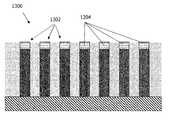
- FIG. 13illustrates a structure 1300 that includes address decoder diodes 1302 formed in accordance with an embodiment of the invention.
- the storage material 802is deposited in all exposed recesses 402 , as described above, corresponding to the address decoder diodes 1302 , conventional diodes 1202 , and/or memory cell diodes 800 .
- the address decoder diodes 1302 and conventional diodesmay not require the storage material 802 , however, and it may be removed from the recesses 402 corresponding to those devices.
- the areas of the substrate 104 corresponding to the vias 1102 and/or the memory storage cells 800are masked, and an appropriate etching step is performed to remove the unmasked storage material 802 .
- a metal layer 1304may be deposited that fills the newly-etched recesses 402 corresponding to the address decoder 1302 and conventional diodes 1202 to make contact therewith.
- the deposited metalmay also contact the memory cells 800 and vias 1002 and thereafter patterned and etched to form circuit interconnects.
- memory cells 800may be altered, and is not critical to the present invention. All or some of these components may be created and connected without adding critical-dimension photolithography masks, in accordance with embodiments of the invention.
- Table 1shows an exemplary ten-mask process flow for fabricating a memory device as described above.
- the photomask steps listed herein, and the order in which they occur,are not meant to be limiting, and other steps, in accordance with embodiments of the invention, are contemplated.
- the stepsare described using photolithography, but other kinds of lithography (such as imprint or e-beam lithography) may be used instead of or in addition to photolithography.
- shallow-trench isolation regionsare created to define the active areas of a silicon wafer using one of many available photolithographic patterning or printing techniques, such as contact printing, proximity printing, or projection printing (including non-optical methods such as extreme-UV lithography).
- the silicon waferis etched to create trenches that are filled with an isolating material such as silicon dioxide. Once filled, some or all of the remaining material above the surface is removed by dry etching, wet etching, and/or chemical mechanical polishing.
- the silicon dioxide in the trenchesisolates device elements on the die. This process is known as shallow trench isolation (“STI”).
- a layeris grown or deposited on the substrate to be used as a transistor gate.
- the thickness of this materialmay be dependent on the operating characteristics of the transistors to be used in the memory device.
- a layer of amorphous silicon, crystalline silicon, polycrystalline silicon, or other suitable electrode materialis deposited on the transistor gate material.
- the resulting structureis patterned using photolithography and etched to form a transistor gate.
- the gateis then encapsulated by an isolating material deposition. This layer is typically thinner than the thickness of the transistor electrode and is subsequently etched. Because the thickness is less than that of the electrode, a fence may remain along the sidewall of the electrode, thereby forming spacers.
- the waferundergoes a doping step which may be performed, for example, by ion implantation. After doping, the wafer undergoes a thermal cycle of sufficiently high temperature that the dopant species interstitially substitutes an atom in the substrate.
- the dopant species to be chosenis dictated by the operational characteristics desired and the resultant material resistivity required for transistor operation, thereby forming a highly doped drain (“HDD”).
- a second dopingknown as lightly doped drain (“LDD”) doping
- LDDlightly doped drain
- Another layersuch as amorphous silicon, epitaxial silicon, polycrystalline silicon, and/or silicon dioxide, is then deposited. After deposition, a CMP step is performed to remove the topography generated by the existing transistor elements and the deposition.
- the pillars 102are formed.
- a photolithography stepis used to print structures on the wafer that are thereafter etched to generate the pillars 102 .
- the area surrounding the pillars 102is then filled with an isolating layer 106 , such as high-density plasma (“HDP”) oxide and subsequently polished (e.g., by CMP) to form a co-planar surface between the pillars 102 and the surrounding isolation material 106 .
- HDPhigh-density plasma
- a fourth photomask stepthe planar surface is processed through another photolithography step to cover and protect active memory elements 802 from subsequent etch processes, which may partially etch the exposed pillars 102 .
- a fifth photomask stepcovers all active memory elements and partially etched pillars. An etch step then etches the pillars 102 that are exposed to create vias 1102 .
- all of the protective photomasking layer(s)is/are removed to fill or overfill the partially and completely etched pillars with a conductive film(s) to create layer-to-layer electrical contacts.
- the conductive filmmay then be processed with a CMP step to remove conductive film on the wafer surface, such that the conductive film remains only in the locations required for proper device electrical connection.
- an etchis used to partially etch the exposed memory element pillars.
- the pillar recesses or voidsare then filled with an isolating material such as silicon nitride and subsequently etched to form a spacer fence surrounding the recess. This spacer reduces the cross-sectional area of the recess.
- a reversible memory storage materialsuch as a phase change alloy is then deposited to fill the remaining void above the memory element pillar.
- the waferis then polished to remove memory-element material from the wafer such that the conductive film remains only in the locations required for proper device electrical connection.
- an isolating material deposited on the waferis patterned and etched to define trenches that will be filled with a conductive film such as tantalum and/or copper.
- the wafermay then be polished (e.g., by CMP) to remove the conductive film above the surface of the isolating layer to form first-level electrical conduction paths (“Metal 1”) between the memory elements, decoding elements, contacts, and/or transistor elements. This process is known as damascene metallization.
- a seventh photomask stepif additional conduction paths are required, another layer of isolating film may be deposited, printed, and etched to create via holes or contacts. These holes may then be filled with conductive film such as copper and/or tungsten to form electrical contacts or vias/plugs.
- an isolating layeris deposited, patterned, etched filled with conductive film, and polished (e.g., by CMP) to produce a second planar level of electrical conduction paths (“Metal 2”).
- the Metal 2 layermay connect to the “Metal 1” layer through the vias to allow additional connectivity to device elements. This process can be replicated multiple times depending on the desired operating characteristics.
- an isolating layeris deposited, masked, etched, and filled with a conductive film such as aluminum and/or an aluminum-copper alloy.
- the conductive filmis patterned and etched to provide an electrical conduction path between it and the underlying conductive film. This process is typically referred to as “bondpad” because it creates a layer to allow bonding of wiring between the operational memory device and the instrument being used to access the memory device.
- Table 2shows, in an alternative embodiment, an eight-mask process flow for fabricating a memory device as described above.
- the eight-mask process floweliminates the seventh and eighth photomask steps from the above-described ten-mask process flow (the formation of Metal 1-to-Metal 2 vias and of Metal 2, respectively) but is otherwise similar.
Landscapes
- Engineering & Computer Science (AREA)
- Manufacturing & Machinery (AREA)
- Semiconductor Memories (AREA)
Abstract
Description
- This application claims priority to and the benefit of U.S. Provisional Patent Application Ser. No. 61/089,625, filed on Aug. 18, 2008, which is hereby incorporated herein by reference in its entirety.
- The present invention relates, in various embodiments, to the manufacture and processing of semiconductor devices, and, more particularly, to methods for fabricating switching devices for solid-state semiconductor memory applications.
- In many types of diode-based solid-state memory, each memory element includes a p-n junction diode. A switching device (that includes, for example, a phase-change material) may be combined with the p-n junction diode to create a reversibly switching, re-programmable (i.e., rewritable or read-write) phase-change random-access memory (“PCRAM”) element. The switching device is typically formed in a recess adjacent to each p-n junction diode. In the prior art, the recess is formed using a subtractive process wherein at least one film layer is deposited, masked with a lithographic process, and partially removed with chemical etching. A conventional complementary metal-oxide-silicon (“CMOS”) based phase-change memory requires sixteen or more masks.
- Other PCRAM processes may require even more photomask steps. Each photomask adds to the cost, complexity, time, and likelihood of failure of the overall device processing. A need exists, therefore, for a PCRAM processing method that uses fewer photomask steps and is thus cheaper, simpler, faster, and more robust than existing processes.
- Embodiments of the present invention include processing methods for a PCRAM device that eliminate the need for additional steps, films, and/or lithography in the fabrication of the recesses used for the switching devices required for each PCRAM memory cell. Pillars of a diode material, surrounded by an isolating material, are first formed. A top surface of the pillars is polished, and the self-aligned recesses may be formed thereon by an etch that reacts with the pillars and isolating material at different rates. Once the recesses are formed, a phase-change alloy may be deposited therein and subsequently operate as switching device for a diode in each memory cell. By eliminating unnecessary layers and lithographic processing steps, embodiments of the invention simplify PCRAM processing and render it less expensive.
- In general, in a first aspect, embodiments of the invention feature a method for forming a non-volatile rewritable memory device. Pillars of material are formed and surrounded by isolating material, and substantially coplanar top surfaces are formed of the pillars and the isolating material. The pillar material and the isolating material are simultaneously etched, the pillar material being etched at a greater rate than the isolating material to form recesses over the pillars. The recesses are filled and circuit elements that include the filled recesses are formed.
- The substantially coplanar top surfaces may be formed by polishing. The pillars and the isolating material may be formed lithographically using fewer than sixteen masks, ten or fewer masks, or eight or fewer masks. The circuit elements may include a non-volatile memory cell, a diode, and/or a via. The step of etching may include or consist of reactive-ion etching, which may include chlorine etching. The pillars of material may include silicon, amorphous silicon, and/or polysilicon. Forming the pillars of material may include epitaxial deposition. The isolating material may include or consist essentially of a dielectric.
- In general, in another aspect, embodiments of the invention feature a method for fabricating an electronic device. An array of pillars is formed, and each pillar includes a diode material and is substantially surrounded by an insulating material. The array of pillars is planarized to expose a top surface of each pillar. An upper portion of each pillar is removed to form a recess thereover. A phase-change material is formed within each recess.
- Each pillar may include an etch-stop layer, and the step of removing an upper portion of each pillar may include exposing the etch-stop layer. The phase-change material may include a chalcogenide alloy. A spacer may be formed within each recess before forming the phase-change material, and the spacer may include or consist of an insulating material. The diode material may include or consist of silicon.
- In general, in another aspect, embodiments of the invention feature a method for fabricating a memory device. The method includes depositing phase-change or resistive-change material, and the memory device is formed lithographically using sixteen or fewer masks. The memory device may also be formed lithographially using ten, eight, or fewer masks.
- These and other objects, along with advantages and features of the embodiments of the present invention herein disclosed, will become more apparent through reference to the following description, the accompanying drawings, and the claims. Furthermore, it is to be understood that the features of the various embodiments described herein are not mutually exclusive and can exist in various combinations and permutations.
- In the drawings, like reference characters generally refer to the same parts throughout the different views. Also, the drawings are not necessarily to scale, emphasis instead generally being placed upon illustrating the principles of the invention. In the following description, various embodiments of the present invention are described with reference to the following enlarged, schematic cross-sections, in which:
FIG. 1 illustrates the deposition of an isolation layer on pillars;FIG. 2 illustrates the planarization process of an isolation layer and pillars;FIG. 3 illustrates isolation layer patterning to generate pillar holes;FIG. 4 illustrates the fill of holes with a pillar materialFIG. 5 illustrates the pillar etching process and the formation of recesses;FIG. 6 illustrates recess creation without an etch-stop layer;FIG. 7 illustrates recess creation with an etch-stop layer;FIG. 8 illustrates the formation of a memory element;FIG. 9 illustrates the complete etch of a pillar;FIG. 10 illustrates via holes formed in pillar holes;FIG. 11 illustrates a contact made by filling the via with a conductive film;FIG. 12 illustrates the formation of a conventional diode device; andFIG. 13 illustrates a decoding element.- Embodiments of the present invention reduce the number of films and lithography steps used in the formation of a recess in a PCRAM element. The recess may be formed by first planarizing, e.g., by chemical-mechanical polishing (“CMP”), an insulating layer over a substrate and the diodes (fabricated therein) to create a substantially planar surface. Then, upper portions of the diode material, e.g., silicon or an alloy thereof, are removed by selective etching. Using a selective etch process, the diode material is removed at a faster rate than is the insulating layer, thereby forming a self-aligned recess immediately above and adjacent to the diode. A chalcogenide or other suitable material may then be formed within the recess.
FIG. 1 illustrates astructure 100 that includes a series ofpillars 102 formed on asubstrate 104 and separated by an isolatingmaterial 106. Thepillars 102 may be generally upright structures that are relatively slender in proportion to their height. More generally, thepillars 102 may have any suitable aspect ratio, including those in which their width exceeds their height, and may have any desired cross-section. Thepillars 102 are typically formed by photolithographic patterning techniques and chemical etching, such as reactive ion etching (“RIE”). Thepillars 102 may be formed of a semiconducting material such as silicon, polysilicon, amorphous silicon, or alloys thereof. Thesubstrate 104 may include or consist of an insulating material, bulk silicon, metal conductors, and/or paths and patterns of other conductive material, such as a doped semiconductor. The isolatingmaterial 106, which may be an electrical insulator such as silicon dioxide, is deposited to surround the formedpillars 102. The combination of deposited pillar material and the material in thesubstrate 104 under a given pillar location may define the electrical characteristics of thepillars 102.- The above-described process (e.g., first forming the
pillars 102 and adding the insulatingmaterial 106 thereafter) allows the formation of complex pillar structures. For example, thepillars 102 may include epitaxially grown layers to form, e.g., a film stack with complex junction designs. FIG. 2 illustrates astructure 200 formed by processing (e.g., polishing) a top surface of thestructure 100 by, for example, CMP to create a substantially planartop surface 202. The polishing may primarily remove the isolatingmaterial 106 and may stop or be stopped generally when thetops 204 of thepillars 102 are reached.FIGS. 3 and 4 illustrate analternative embodiment 300 in which the isolatingmaterial 106 is first deposited and, using photolithographic patterning techniques and chemical etching, holes302 are defined and etched therein. An etch-stop material 304 may be used to prevent portions of the isolatingmaterial 106 from being removed. As shown inFIG. 4 , theholes 302 may be subsequently filled with thepillar material 102. A top surface of thestructure 300 may then be polished by CMP to produce thestructure 200 depicted inFIG. 2 . In this case, however, the polishing is performed primarily upon thepillar material 102 and stops or is stopped generally when a top surface of the isolatingmaterial 106 is reached. This halt to the process may be achieved either by timing the polishing process or by selecting a polishing agent (e.g., polishing slurry and polishing pad) that polishes a primary material (e.g., the pillar material102) selectively to a secondary material (e.g., the isolating material106). In other words, the polishing process may polish the primary material at a greater rate than the secondary material so as to effectively stop, or significantly slow down, when the secondary material becomes exposed. Slurries or polishing agents having material selectivity are well known and understood by those skilled in the art of CMP. Typically, depositing the isolatingmaterial 106 first and then etching and filling the pillar holes is less desirable because of the difficulty in patterning and etching very small (e.g., critical dimension) holes and filling such small holes without forming voids.FIGS. 5 and 6 illustrate the formation ofrecesses 402 of depth d in thestructure 500 by using a maskless (e.g., self-aligned)selective pillar etch 404. The etch is selective, etching thepillar material 102 more rapidly than the surrounding insulatingmaterial 106. Etches having material selectivity are well known and understood by those skilled in the art of chemical etching. For example, a chlorine-based RIE etch may etch the pillar material102 (which may include or consist of silicon, polysilicon, and/or amorphous silicon) approximately ten times or faster than the surrounding insulating material106 (which may include or consist of silicon dioxide). This self-aligned etching process enables the creation of therecesses 402 without additional masking or material layers and without additional photolithographic steps.FIG. 6 illustrates astructure 600 havingrecesses 402 formed by the above-described process.FIG. 7 illustrates, in one embodiment, astructure 700 having anetch stop layer 702 on eachpillar 102. Therecesses 402 may be created at many different points across a die or wafer, and controlling the etching process across such a large area to producerecesses 402 of similar depth may be difficult. Accordingly, the etch-stop layer 702 may permit greater control of therecess 402 depth across the die and/or wafer by providing a stopping point for the etch chemistry, such that allpillars 102 are etched to a similar or substantially identical depth. In one embodiment, a multi-layer stack is deposited during the creation of thepillars 102 to facilitate formation of the etch-stop layer 702. For example, referring also to thestructure 300 shown inFIG. 3 , a lower portion of thepillars 102 may be formed by epitaxially depositing silicon in theholes 302 in the isolatingmaterial 106. The epitaxial process may be finely controlled to producepillars 102 of a known height. The etch-stop layer702 (e.g., a silicon dioxide layer) may then be formed on the epitaxially deposited silicon, and an additional amorphous or polycrystalline silicon layer may be formed on the etch-stop layer 702. The thickness of the additional amorphous or polycrystalline silicon layer may be approximately equal to the desired depth of therecesses 402, and may be removed in later processing steps to formrecesses 402 having the desired depth. The thickness of the additional amorphous or polycrystalline silicon layer may allow for some over-polishing that would otherwise reduce the depth of therecess 402, as is well known and understood to those skilled in the art.- In one embodiment, the etch-
stop layer 702 is formed based on thestructure 100 ofFIG. 1 . In this embodiment, the pillar material is first deposited, and layers of the etch-stop material 702 and additional amorphous or polycrystalline silicon are deposited thereon. The layer stack may thereafter be patterned to form pillars102 (that include the etch stop-material702) separated by theisolation material 106. The etch-stop material 702 may then be used in an etching process to produce therecesses 402, as described above. FIG. 8 illustrates use of the structures described above to form data-storage elements. As illustrated, astructure 800 includes a data-storage material802 (e.g., a phase-change alloy) deposited on thepillars 102 in therecesses 402. The data-storage material 802 makes an electrical connection with the semiconductor material in thepillar 102, thereby operating in series with the diode formed by thepillar 102 and thesubstrate 104 to provide an information storage device. The data-storage material 802 may be any material having a memory or information-retaining property, such as a resistive change material or a phase change material (such as a chalcogenide alloy or an ovonic alloy). Thedata storage material 802 may function as a switch in the memory cell.- In one embodiment, a spacer layer (not shown) is formed within a
recess 402 prior to deposition of the data-storage material 802. The spacer layer is similar to spacers formed about the gate of an FET transistor and well known to those skilled in the art. The spacer may be formed by conformally depositing a spacer material (e.g., an insulator such as silicon dioxide or silicon nitride) in arecess 402. The spacer material is thereafter etched back, thereby removing it from the wafer surface and the bottom of the recess, while leaving a portion of the spacer material on the sidewalls of therecess 402. The presence of the spacer layer causes the later-deposited data-storage material 802 to have a smaller cross-sectional area, thus concentrating any current passing therethrough and creating a higher effective current density during device operation. - In other embodiments, shown in
FIGS. 9-13 , an expanded version of the pillar etch (as described above) may be used to simultaneously form other components, such as contact vias, address decoder diodes, and/or conventional diodes (i.e., diodes without data-storage material). For example, as shown inFIGS. 9-11 , contact vias may be formed by masking (i.e., covering, typically using a large-geometry, non-critical photolithographic mask) a first area (not shown) of thesubstrate 104 where memory storage cell diodes and conventional diodes are to be formed and thereafter etching a second, unmaskedarea 900 of thesubstrate 104, as illustrated inFIG. 9 .FIG. 10 shows the etchedstructure 1000, in which thosepillars 102 where vias are to be created are etched entirely away to formdeep recesses 1002, thereby exposing atop surface 1004 of thesubstrate 104.FIG. 11 illustrates thedeep recesses 1002 filled in byvias 1102 formed by, for example, a damascene metal process that returns thesurface 1104 to a planar condition. Other components (such as address decoders, conventional diodes, and/or memory cells) may use one or moreadjacent vias 1102 to make an electrical connection to a portion of the component disposed below thesurface 1104 and not otherwise accessible. Upper metal layers may make an electrical connection to a top surface of a via1102 adjancent to a component to connect the component to other circuits on the wafer or die. - In one embodiment, the pillar material is not totally removed (i.e., a
surface 1004 of thesubstrate 104 is not exposed) before the formation of a via1102. Instead, only enough of the pillar material is removed so that thepillar 102 is not large enough to form a rectifying junction with thesubstrate 104 or other layer. In other words, the etch proceeds to a point on thepillar 102 below a potential rectifying junction. The remaining portion of thepillar 102 thus forms a simple ohmic contact to a conductive material in thesubstrate 104. Allowing a small portion of thepillar 102 to remain may decrease the cost, complexity, and/or failure rate of this etching step. FIG. 12 illustrates astructure 1200 that includes non-storage-element (i.e., conventional) p-n and/orp-i-n junction diodes 1202. Theconventional diodes 1202 may be used in a variety of circuit applications, such as in memory-cell current-steering devices. Theconventional diodes 1202 may be formed by depositing or doping asemiconductor material 1202 into therecesses 402 ontop surfaces 1206 of thepillars 102. In one embodiment, thepillar 102 is an n-type semiconductor and the deposited or dopedmaterial 1202 is p-type; in another embodiment, thepillar 102 is p-type and the deposited or dopedmaterial 1202 is n-type. An insulator layer (not shown) may be formed between the p-type and n-type semiconductor material to create a p-i-n diode. For example, thesubstrate 104 may include n+-type silicon and thepillar 104 may include intrinsic silicon. Prior to deposition of the data-storage material 802, an ion implantation step may dope thetop portion 1202 of theintrinsic silicon pillar 102 to form p+-type material, thereby creating a p-i-n diode.- In one embodiment, a
conventional diode 1202 is masked during later processing steps to preserve its standard p-n or p-i-n structure. Alternatively, a top portion of aconventional diode 1202 may be partially etched and the resulting opening be filled with a conductive material (such as metal); both cases result in a diode-like rectifying contact. - The
conventional diodes 1202 may be combined in an address-decoder array in a PCRAM memory. In one embodiment, the address-decoder array receives an encoded address and enables one of a plurality of array bit or word lines, thereby selecting an element in a storage array. The storage element may be the data-storage material 802, described above, and its underlying diode. FIG. 13 illustrates astructure 1300 that includesaddress decoder diodes 1302 formed in accordance with an embodiment of the invention. Thestorage material 802 is deposited in all exposedrecesses 402, as described above, corresponding to theaddress decoder diodes 1302,conventional diodes 1202, and/ormemory cell diodes 800. Theaddress decoder diodes 1302 and conventional diodes may not require thestorage material 802, however, and it may be removed from therecesses 402 corresponding to those devices. In one embodiment, the areas of thesubstrate 104 corresponding to thevias 1102 and/or thememory storage cells 800 are masked, and an appropriate etching step is performed to remove the unmaskedstorage material 802. The mask is thereafter removed, and ametal layer 1304 may be deposited that fills the newly-etchedrecesses 402 corresponding to theaddress decoder 1302 andconventional diodes 1202 to make contact therewith. The deposited metal may also contact thememory cells 800 andvias 1002 and thereafter patterned and etched to form circuit interconnects.- As one skilled in the art will realize, the order of formation of
memory cells 800,address decoder diodes 1302,conventional diodes 1202, and vias1102 may be altered, and is not critical to the present invention. All or some of these components may be created and connected without adding critical-dimension photolithography masks, in accordance with embodiments of the invention. - Table 1 shows an exemplary ten-mask process flow for fabricating a memory device as described above. The photomask steps listed herein, and the order in which they occur, are not meant to be limiting, and other steps, in accordance with embodiments of the invention, are contemplated. The steps are described using photolithography, but other kinds of lithography (such as imprint or e-beam lithography) may be used instead of or in addition to photolithography.
TABLE 1 Ten-Mask Process Flow Photomask Number Name Description Usage 1 STI Shallow Trench Isolation Define active area 2 GATE Transistor Gate Define NMOS transistor gate 3 VP Vertical Pillar Define vertical pillars 4 DPE Decoder Pillar Etch Define areas protected during decoder element etch 5 CT Contact Define areas where pillars will be completely etched 6 M1 Metal 1 Define electrical conduction paths in first level 7 V1 Via 1 Define areas protected during via hole etch 8 M2 Metal 2 Define electrical conduction paths in second level 9 PAD Bondpad Open Define areas protected during the isolation layer etch 10 M3 Metal 3 Define areas protected during the conductive layer etch - In a first photomask step, shallow-trench isolation regions are created to define the active areas of a silicon wafer using one of many available photolithographic patterning or printing techniques, such as contact printing, proximity printing, or projection printing (including non-optical methods such as extreme-UV lithography). The silicon wafer is etched to create trenches that are filled with an isolating material such as silicon dioxide. Once filled, some or all of the remaining material above the surface is removed by dry etching, wet etching, and/or chemical mechanical polishing. The silicon dioxide in the trenches isolates device elements on the die. This process is known as shallow trench isolation (“STI”).
- In a second photomask step, a layer is grown or deposited on the substrate to be used as a transistor gate. The thickness of this material may be dependent on the operating characteristics of the transistors to be used in the memory device. Thereafter, a layer of amorphous silicon, crystalline silicon, polycrystalline silicon, or other suitable electrode material is deposited on the transistor gate material. The resulting structure is patterned using photolithography and etched to form a transistor gate. The gate is then encapsulated by an isolating material deposition. This layer is typically thinner than the thickness of the transistor electrode and is subsequently etched. Because the thickness is less than that of the electrode, a fence may remain along the sidewall of the electrode, thereby forming spacers. After spacer formation, the wafer undergoes a doping step which may be performed, for example, by ion implantation. After doping, the wafer undergoes a thermal cycle of sufficiently high temperature that the dopant species interstitially substitutes an atom in the substrate. The dopant species to be chosen is dictated by the operational characteristics desired and the resultant material resistivity required for transistor operation, thereby forming a highly doped drain (“HDD”). Once the HDD doping is completed, a second doping, known as lightly doped drain (“LDD”) doping, is used to improve the transistor operational characteristics by increasing the resistivity between the gate and drain interface. Another layer, such as amorphous silicon, epitaxial silicon, polycrystalline silicon, and/or silicon dioxide, is then deposited. After deposition, a CMP step is performed to remove the topography generated by the existing transistor elements and the deposition.
- In a third photomask step, the
pillars 102 are formed. After the CMP step described above, a photolithography step is used to print structures on the wafer that are thereafter etched to generate thepillars 102. The area surrounding thepillars 102 is then filled with an isolatinglayer 106, such as high-density plasma (“HDP”) oxide and subsequently polished (e.g., by CMP) to form a co-planar surface between thepillars 102 and the surroundingisolation material 106. - In a fourth photomask step, the planar surface is processed through another photolithography step to cover and protect
active memory elements 802 from subsequent etch processes, which may partially etch the exposedpillars 102. A fifth photomask step covers all active memory elements and partially etched pillars. An etch step then etches thepillars 102 that are exposed to createvias 1102. Next, all of the protective photomasking layer(s) is/are removed to fill or overfill the partially and completely etched pillars with a conductive film(s) to create layer-to-layer electrical contacts. The conductive film may then be processed with a CMP step to remove conductive film on the wafer surface, such that the conductive film remains only in the locations required for proper device electrical connection. - After the CMP step, an etch is used to partially etch the exposed memory element pillars. The pillar recesses or voids are then filled with an isolating material such as silicon nitride and subsequently etched to form a spacer fence surrounding the recess. This spacer reduces the cross-sectional area of the recess. A reversible memory storage material such as a phase change alloy is then deposited to fill the remaining void above the memory element pillar. The wafer is then polished to remove memory-element material from the wafer such that the conductive film remains only in the locations required for proper device electrical connection.
- In a sixth photomask step, an isolating material deposited on the wafer is patterned and etched to define trenches that will be filled with a conductive film such as tantalum and/or copper. The wafer may then be polished (e.g., by CMP) to remove the conductive film above the surface of the isolating layer to form first-level electrical conduction paths (“Metal 1”) between the memory elements, decoding elements, contacts, and/or transistor elements. This process is known as damascene metallization.
- In a seventh photomask step, if additional conduction paths are required, another layer of isolating film may be deposited, printed, and etched to create via holes or contacts. These holes may then be filled with conductive film such as copper and/or tungsten to form electrical contacts or vias/plugs. In an eighth photomask step, an isolating layer is deposited, patterned, etched filled with conductive film, and polished (e.g., by CMP) to produce a second planar level of electrical conduction paths (“Metal 2”). The Metal 2 layer may connect to the “Metal 1” layer through the vias to allow additional connectivity to device elements. This process can be replicated multiple times depending on the desired operating characteristics.
- In a ninth photomask step, for the final planar level, an isolating layer is deposited, masked, etched, and filled with a conductive film such as aluminum and/or an aluminum-copper alloy. In a tenth photomask step, the conductive film is patterned and etched to provide an electrical conduction path between it and the underlying conductive film. This process is typically referred to as “bondpad” because it creates a layer to allow bonding of wiring between the operational memory device and the instrument being used to access the memory device.
- Table 2 shows, in an alternative embodiment, an eight-mask process flow for fabricating a memory device as described above. The eight-mask process flow eliminates the seventh and eighth photomask steps from the above-described ten-mask process flow (the formation of Metal 1-to-Metal 2 vias and of Metal 2, respectively) but is otherwise similar.
TABLE 2 Eight-Mask Process Flow Photomask Number Name Description Usage 1 STI Shallow Trench Isolation Define active area 2 GATE Transistor Gate Define NMOS transistor gate 3 VP Vertical Pillar Define vertical pillars 4 DPE Decoder Pillar Etch Define areas protected during decoder element etch 5 CT Contact Define areas where pillars will be completely etched 6 M1 Metal 1 Define electrical conduction paths in first level 7 PAD Bondpad Open Define areas protected during the isolation layer etch 8 M3 Metal 3 Define areas protected during the conductive layer etch - Having described certain embodiments of the invention, it will be apparent to those of ordinary skill in the art that other embodiments incorporating the concepts disclosed herein may be used without departing from the spirit and scope of the invention. Accordingly, the described embodiments are to be considered in all respects as only illustrative and not restrictive.
Claims (22)
Priority Applications (1)
| Application Number | Priority Date | Filing Date | Title |
|---|---|---|---|
| US12/543,086US8455298B2 (en) | 2008-08-18 | 2009-08-18 | Method for forming self-aligned phase-change semiconductor diode memory |
Applications Claiming Priority (2)
| Application Number | Priority Date | Filing Date | Title |
|---|---|---|---|
| US8962508P | 2008-08-18 | 2008-08-18 | |
| US12/543,086US8455298B2 (en) | 2008-08-18 | 2009-08-18 | Method for forming self-aligned phase-change semiconductor diode memory |
Publications (2)
| Publication Number | Publication Date |
|---|---|
| US20100047995A1true US20100047995A1 (en) | 2010-02-25 |
| US8455298B2 US8455298B2 (en) | 2013-06-04 |
Family
ID=41696764
Family Applications (1)
| Application Number | Title | Priority Date | Filing Date |
|---|---|---|---|
| US12/543,086Expired - Fee RelatedUS8455298B2 (en) | 2008-08-18 | 2009-08-18 | Method for forming self-aligned phase-change semiconductor diode memory |
Country Status (2)
| Country | Link |
|---|---|
| US (1) | US8455298B2 (en) |
| WO (1) | WO2010022036A2 (en) |
Cited By (5)
| Publication number | Priority date | Publication date | Assignee | Title |
|---|---|---|---|---|
| US8284597B2 (en) | 2010-05-06 | 2012-10-09 | Macronix International Co., Ltd. | Diode memory |
| US20150145065A1 (en)* | 2013-11-25 | 2015-05-28 | International Business Machines Corporation | finFET Isolation by Selective Cyclic Etch |
| US9646880B1 (en)* | 2016-01-14 | 2017-05-09 | Sandisk Technologies Llc | Monolithic three dimensional memory arrays formed using sacrificial polysilicon pillars |
| WO2020185363A1 (en)* | 2019-03-11 | 2020-09-17 | Micron Technology, Inc. | Dimension control for raised lines |
| US11024735B2 (en)* | 2017-12-22 | 2021-06-01 | Micron Technology, Inc. | Methods of forming integrated circuitry |
Families Citing this family (1)
| Publication number | Priority date | Publication date | Assignee | Title |
|---|---|---|---|---|
| KR102316317B1 (en) | 2015-06-05 | 2021-10-22 | 삼성전자주식회사 | Semiconductor devices and methods of manufacturing the same |
Citations (18)
| Publication number | Priority date | Publication date | Assignee | Title |
|---|---|---|---|---|
| US4321661A (en)* | 1980-12-23 | 1982-03-23 | Gte Laboratories Incorporated | Apparatus for charging a capacitor |
| US5889694A (en)* | 1996-03-05 | 1999-03-30 | Shepard; Daniel R. | Dual-addressed rectifier storage device |
| US6198645B1 (en)* | 1998-07-02 | 2001-03-06 | National Semiconductor Corporation | Buck and boost switched capacitor gain stage with optional shared rest state |
| US6306740B1 (en)* | 1998-08-10 | 2001-10-23 | Yamaha Corporation | Manufacture of field emission element |
| US20030016553A1 (en)* | 1998-11-16 | 2003-01-23 | Vivek Subramanian | Vertically stacked field programmable nonvolatile memory and method of fabrication |
| US6586327B2 (en)* | 2000-09-27 | 2003-07-01 | Nup2 Incorporated | Fabrication of semiconductor devices |
| US6861694B2 (en)* | 1996-11-06 | 2005-03-01 | Fujitsu Limited | Semiconductor device and method for fabricating the same |
| US6952030B2 (en)* | 2002-12-19 | 2005-10-04 | Matrix Semiconductor, Inc. | High-density three-dimensional memory cell |
| US20060062043A1 (en)* | 2004-08-23 | 2006-03-23 | Thomas Roehr | CBRAM memory cell arrangement and method for programming CBRAM memory cells |
| US20070034921A1 (en)* | 2005-08-09 | 2007-02-15 | Micron Technology, Inc. | Access transistor for memory device |
| US20080078984A1 (en)* | 2006-09-29 | 2008-04-03 | Samsung Electronics Co., Ltd. | Semiconductor device and method of fabricating the same |
| US20080116441A1 (en)* | 2006-11-16 | 2008-05-22 | Usha Raghuram | Nonvolatile phase change memory cell having a reduced contact area |
| US20080175032A1 (en)* | 2007-01-23 | 2008-07-24 | Kabushiki Kaisha Toshiba | Semiconductor memory and method for manufacturing the same |
| US20080197334A1 (en)* | 2007-02-21 | 2008-08-21 | Macronix International Co., Ltd. | Phase Change Memory Cell with Heater and Method for Fabricating the Same |
| US20090001337A1 (en)* | 2007-06-29 | 2009-01-01 | Toshiharu Furukawa | Phase Change Memory Cell with Vertical Transistor |
| US20090261313A1 (en)* | 2008-04-22 | 2009-10-22 | Macronix International Co., Ltd. | Memory cell having a buried phase change region and method for fabricating the same |
| US8022381B2 (en)* | 2003-04-03 | 2011-09-20 | Kabushiki Kaisha Toshiba | Phase change memory device |
| US8148230B2 (en)* | 2009-07-15 | 2012-04-03 | Sandisk 3D Llc | Method of making damascene diodes using selective etching methods |
Family Cites Families (8)
| Publication number | Priority date | Publication date | Assignee | Title |
|---|---|---|---|---|
| US5103144A (en) | 1990-10-01 | 1992-04-07 | Raytheon Company | Brightness control for flat panel display |
| US6621096B2 (en) | 2001-05-21 | 2003-09-16 | Hewlett-Packard Develpoment Company, L.P. | Device isolation process flow for ARS system |
| US6628052B2 (en) | 2001-10-05 | 2003-09-30 | Hewlett-Packard Development Company, L.P. | Enhanced electron field emitter spindt tip and method for fabricating enhanced spindt tips |
| US6961299B2 (en) | 2002-12-05 | 2005-11-01 | Hewlett-Packard Development Company, L.P. | Storage device |
| US7189626B2 (en)* | 2004-11-03 | 2007-03-13 | Micron Technology, Inc. | Electroless plating of metal caps for chalcogenide-based memory devices |
| WO2007116749A1 (en)* | 2006-03-30 | 2007-10-18 | Matsushita Electric Industrial Co., Ltd. | Nonvolatile memory element and its manufacturing method |
| US7443712B2 (en) | 2006-09-07 | 2008-10-28 | Spansion Llc | Memory erase management system |
| WO2008061194A1 (en)* | 2006-11-16 | 2008-05-22 | Sandisk 3D Llc | Nonvolatile phase change memory cell having a reduced contact area and method of making |
- 2009
- 2009-08-18WOPCT/US2009/054137patent/WO2010022036A2/enactiveApplication Filing
- 2009-08-18USUS12/543,086patent/US8455298B2/ennot_activeExpired - Fee Related
Patent Citations (19)
| Publication number | Priority date | Publication date | Assignee | Title |
|---|---|---|---|---|
| US4321661A (en)* | 1980-12-23 | 1982-03-23 | Gte Laboratories Incorporated | Apparatus for charging a capacitor |
| US5889694A (en)* | 1996-03-05 | 1999-03-30 | Shepard; Daniel R. | Dual-addressed rectifier storage device |
| US6861694B2 (en)* | 1996-11-06 | 2005-03-01 | Fujitsu Limited | Semiconductor device and method for fabricating the same |
| US6198645B1 (en)* | 1998-07-02 | 2001-03-06 | National Semiconductor Corporation | Buck and boost switched capacitor gain stage with optional shared rest state |
| US6306740B1 (en)* | 1998-08-10 | 2001-10-23 | Yamaha Corporation | Manufacture of field emission element |
| US20030016553A1 (en)* | 1998-11-16 | 2003-01-23 | Vivek Subramanian | Vertically stacked field programmable nonvolatile memory and method of fabrication |
| US6586327B2 (en)* | 2000-09-27 | 2003-07-01 | Nup2 Incorporated | Fabrication of semiconductor devices |
| US6952030B2 (en)* | 2002-12-19 | 2005-10-04 | Matrix Semiconductor, Inc. | High-density three-dimensional memory cell |
| US8022381B2 (en)* | 2003-04-03 | 2011-09-20 | Kabushiki Kaisha Toshiba | Phase change memory device |
| US20060062043A1 (en)* | 2004-08-23 | 2006-03-23 | Thomas Roehr | CBRAM memory cell arrangement and method for programming CBRAM memory cells |
| US20070034921A1 (en)* | 2005-08-09 | 2007-02-15 | Micron Technology, Inc. | Access transistor for memory device |
| US20080078984A1 (en)* | 2006-09-29 | 2008-04-03 | Samsung Electronics Co., Ltd. | Semiconductor device and method of fabricating the same |
| US20080116441A1 (en)* | 2006-11-16 | 2008-05-22 | Usha Raghuram | Nonvolatile phase change memory cell having a reduced contact area |
| US7728318B2 (en)* | 2006-11-16 | 2010-06-01 | Sandisk Corporation | Nonvolatile phase change memory cell having a reduced contact area |
| US20080175032A1 (en)* | 2007-01-23 | 2008-07-24 | Kabushiki Kaisha Toshiba | Semiconductor memory and method for manufacturing the same |
| US20080197334A1 (en)* | 2007-02-21 | 2008-08-21 | Macronix International Co., Ltd. | Phase Change Memory Cell with Heater and Method for Fabricating the Same |
| US20090001337A1 (en)* | 2007-06-29 | 2009-01-01 | Toshiharu Furukawa | Phase Change Memory Cell with Vertical Transistor |
| US20090261313A1 (en)* | 2008-04-22 | 2009-10-22 | Macronix International Co., Ltd. | Memory cell having a buried phase change region and method for fabricating the same |
| US8148230B2 (en)* | 2009-07-15 | 2012-04-03 | Sandisk 3D Llc | Method of making damascene diodes using selective etching methods |
Cited By (10)
| Publication number | Priority date | Publication date | Assignee | Title |
|---|---|---|---|---|
| US8284597B2 (en) | 2010-05-06 | 2012-10-09 | Macronix International Co., Ltd. | Diode memory |
| US20150145065A1 (en)* | 2013-11-25 | 2015-05-28 | International Business Machines Corporation | finFET Isolation by Selective Cyclic Etch |
| US9209178B2 (en)* | 2013-11-25 | 2015-12-08 | International Business Machines Corporation | finFET isolation by selective cyclic etch |
| US9646880B1 (en)* | 2016-01-14 | 2017-05-09 | Sandisk Technologies Llc | Monolithic three dimensional memory arrays formed using sacrificial polysilicon pillars |
| CN108431978A (en)* | 2016-01-14 | 2018-08-21 | 桑迪士克科技有限责任公司 | Monolithic 3D memory array formed using sacrificial polysilicon pillars |
| US11024735B2 (en)* | 2017-12-22 | 2021-06-01 | Micron Technology, Inc. | Methods of forming integrated circuitry |
| US12142680B2 (en) | 2017-12-22 | 2024-11-12 | Micron Technology, Inc. | Transistor structures having conductive structures along pillars of semiconductor material |
| WO2020185363A1 (en)* | 2019-03-11 | 2020-09-17 | Micron Technology, Inc. | Dimension control for raised lines |
| US11121181B2 (en) | 2019-03-11 | 2021-09-14 | Micron Technology, Inc. | Dimension control for raised lines |
| US11758741B2 (en) | 2019-03-11 | 2023-09-12 | Micron Technology, Inc. | Dimension control for raised lines |
Also Published As
| Publication number | Publication date |
|---|---|
| US8455298B2 (en) | 2013-06-04 |
| WO2010022036A2 (en) | 2010-02-25 |
| WO2010022036A3 (en) | 2013-05-30 |
Similar Documents
| Publication | Publication Date | Title |
|---|---|---|
| US10879375B2 (en) | Gate tie-down enablement with inner spacer | |
| US9564433B2 (en) | Semiconductor device with improved contact structure and method of forming same | |
| US10083969B2 (en) | Static random access memory and method of manufacturing the same | |
| US7001846B2 (en) | High-density SOI cross-point memory array and method for fabricating same | |
| JP5139269B2 (en) | High density non-volatile memory arrays fabricated at low temperature including semiconductor diodes. | |
| CN110875352A (en) | Integrated circuit, MRAM cell and method for manufacturing a memory device | |
| US20050029664A1 (en) | Unitary interconnection structures integral with a dielectric layer and fabrication methods thereof | |
| KR20080031663A (en) | How to reduce dielectric overetching using dielectric etch stops on smooth surfaces | |
| US12089390B2 (en) | Cell manufacturing | |
| US8455298B2 (en) | Method for forming self-aligned phase-change semiconductor diode memory | |
| US11824004B2 (en) | Method for fabricating semiconductor device structure with manganese-containing conductive plug | |
| US20230337420A1 (en) | Memory devices and methods of manufacturing thereof | |
| JP2008536300A (en) | Method for reducing dielectric overetching in making contacts to conductive features | |
| JP4827074B2 (en) | High density SOI crosspoint memory array and method for manufacturing the same | |
| US11532554B2 (en) | Interconnect device and method | |
| US20090050867A1 (en) | Feature formed beneath an existing material during fabrication of a semiconductor device and electronic systems comprising the semiconductor device | |
| US12249512B2 (en) | Semiconductor structure with air gap in pattern- dense region and method of manufacturing the same | |
| US6967161B2 (en) | Method and resulting structure for fabricating DRAM cell structure using oxide line spacer | |
| TWI849684B (en) | Semiconductor memory device and method of manufacture | |
| US20250125191A1 (en) | Semiconductor device structure with reduced critical dimension and method for preparing the same | |
| US6870211B1 (en) | Self-aligned array contact for memory cells | |
| US12414305B2 (en) | Transistor, memory device and manufacturing method of memory device | |
| US11690232B2 (en) | High density memory devices with low cell leakage and methods for forming the same | |
| CN112563205A (en) | Method for forming semiconductor device | |
| JP2010245102A (en) | Semiconductor device and manufacturing method thereof |
Legal Events
| Date | Code | Title | Description |
|---|---|---|---|
| AS | Assignment | Owner name:CONTOUR SEMICONDUCTOR, INC.,MASSACHUSETTS Free format text:ASSIGNMENT OF ASSIGNORS INTEREST;ASSIGNORS:APODACA, MAC D.;ZHAO, AILIAN;CHOW, JENN C.;AND OTHERS;SIGNING DATES FROM 20090903 TO 20091106;REEL/FRAME:023494/0388 Owner name:CONTOUR SEMICONDUCTOR, INC., MASSACHUSETTS Free format text:ASSIGNMENT OF ASSIGNORS INTEREST;ASSIGNORS:APODACA, MAC D.;ZHAO, AILIAN;CHOW, JENN C.;AND OTHERS;SIGNING DATES FROM 20090903 TO 20091106;REEL/FRAME:023494/0388 | |
| AS | Assignment | Owner name:STILL RIVER FUND III, LIMITED PARTNERSHIP, MASSACH Free format text:SECURITY AGREEMENT;ASSIGNOR:CONTOUR SEMICONDUCTOR, INC.;REEL/FRAME:029659/0615 Effective date:20130118 Owner name:RUNNING DEER FOUNDATION, MASSACHUSETTS Free format text:SECURITY AGREEMENT;ASSIGNOR:CONTOUR SEMICONDUCTOR, INC.;REEL/FRAME:029659/0615 Effective date:20130118 Owner name:SARAH G. KURZON 2001 REVOCABLE TRUST, NEW HAMPSHIR Free format text:SECURITY AGREEMENT;ASSIGNOR:CONTOUR SEMICONDUCTOR, INC.;REEL/FRAME:029659/0615 Effective date:20130118 Owner name:RUNNING DEER TRUST, MASSACHUSETTS Free format text:SECURITY AGREEMENT;ASSIGNOR:CONTOUR SEMICONDUCTOR, INC.;REEL/FRAME:029659/0615 Effective date:20130118 Owner name:PERRIN, DONALD, MASSACHUSETTS Free format text:SECURITY AGREEMENT;ASSIGNOR:CONTOUR SEMICONDUCTOR, INC.;REEL/FRAME:029659/0615 Effective date:20130118 Owner name:AMERICAN CAPITAL, LTD., MARYLAND Free format text:SECURITY AGREEMENT;ASSIGNOR:CONTOUR SEMICONDUCTOR, INC.;REEL/FRAME:029659/0615 Effective date:20130118 | |
| STCF | Information on status: patent grant | Free format text:PATENTED CASE | |
| AS | Assignment | Owner name:AMERICAN CAPITAL, LTD., MARYLAND Free format text:SECURITY INTEREST;ASSIGNOR:CONTOUR SEMICONDUCTOR, INC.;REEL/FRAME:033063/0617 Effective date:20140530 | |
| AS | Assignment | Owner name:RUNNING DEER FOUNDATION, MASSACHUSETTS Free format text:SECURITY INTEREST;ASSIGNOR:CONTOUR SEMICONDUCTOR, INC.;REEL/FRAME:033204/0428 Effective date:20140620 Owner name:AMERICAN CAPITAL, LTD., MARYLAND Free format text:SECURITY INTEREST;ASSIGNOR:CONTOUR SEMICONDUCTOR, INC.;REEL/FRAME:033204/0428 Effective date:20140620 Owner name:OVONYX, INC., MICHIGAN Free format text:SECURITY INTEREST;ASSIGNOR:CONTOUR SEMICONDUCTOR, INC.;REEL/FRAME:033204/0428 Effective date:20140620 Owner name:SARAH G. KURZON 2001 REVOCABLE TRUST, NEW HAMPSHIR Free format text:SECURITY INTEREST;ASSIGNOR:CONTOUR SEMICONDUCTOR, INC.;REEL/FRAME:033204/0428 Effective date:20140620 Owner name:STILL RIVER FUND III, LIMITED PARTNERSHIP, MASSACH Free format text:SECURITY INTEREST;ASSIGNOR:CONTOUR SEMICONDUCTOR, INC.;REEL/FRAME:033204/0428 Effective date:20140620 Owner name:PERRIN, DONALD, MASSACHUSETTS Free format text:SECURITY INTEREST;ASSIGNOR:CONTOUR SEMICONDUCTOR, INC.;REEL/FRAME:033204/0428 Effective date:20140620 Owner name:RUNNING DEER TRUST, MASSACHUSETTS Free format text:SECURITY INTEREST;ASSIGNOR:CONTOUR SEMICONDUCTOR, INC.;REEL/FRAME:033204/0428 Effective date:20140620 | |
| AS | Assignment | Owner name:CONTOUR SEMICONDUCTOR, INC., MASSACHUSETTS Free format text:RELEASE OF SECURITY INTEREST;ASSIGNOR:AMERICAN CAPITAL, LTD.;REEL/FRAME:033225/0330 Effective date:20140620 | |
| FEPP | Fee payment procedure | Free format text:PAYOR NUMBER ASSIGNED (ORIGINAL EVENT CODE: ASPN); ENTITY STATUS OF PATENT OWNER: LARGE ENTITY | |
| AS | Assignment | Owner name:CONTOUR SEMICONDUCTOR, INC., MASSACHUSETTS Free format text:RELEASE BY SECURED PARTY;ASSIGNORS:AMERICAN CAPITAL, LTD.;STILL RIVER FUND III, LIMITED PARTNERSHIP;SARAH G. KURZON 2001 REVOCABLE TRUST;AND OTHERS;REEL/FRAME:035685/0571 Effective date:20150515 | |
| AS | Assignment | Owner name:CONTOUR SEMICONDUCTOR, INC., MASSACHUSETTS Free format text:RELEASE BY SECURED PARTY;ASSIGNORS:AMERICAN CAPITAL, LTD.;STILL RIVER FUND III, LIMITED PARTNERSHIP;SARAH G. KURZON 2001 REVOCABLE TRUST;AND OTHERS;REEL/FRAME:035749/0956 Effective date:20150515 | |
| AS | Assignment | Owner name:HGST NETHERLANDS B.V., NETHERLANDS Free format text:ASSIGNMENT OF ASSIGNORS INTEREST;ASSIGNOR:CONTOUR SEMICONDUCTOR, INC.;REEL/FRAME:035748/0909 Effective date:20150515 | |
| AS | Assignment | Owner name:HGST, INC., CALIFORNIA Free format text:CORRECTIVE ASSIGNMENT TO CORRECT THE NAME AND ADDRESS OF THE ASSIGNEE PREVIOUSLY RECORDED ON REEL 035748 FRAME 0909. ASSIGNOR(S) HEREBY CONFIRMS THE NAME AND ADDRESS OF THE ASSIGNEE SI HGST, INC.,3403 YERBA BUENA ROAD,SAN JOSE, CA 95135;ASSIGNOR:CONTOUR SEMICONDUCTOR, INC.;REEL/FRAME:035831/0594 Effective date:20150515 | |
| AS | Assignment | Owner name:JPMORGAN CHASE BANK, N.A., AS COLLATERAL AGENT, IL Free format text:SECURITY AGREEMENT;ASSIGNOR:HGST, INC.;REEL/FRAME:039389/0684 Effective date:20160712 | |
| AS | Assignment | Owner name:HGST, INC., CALIFORNIA Free format text:RELEASE BY SECURED PARTY;ASSIGNOR:JPMORGAN CHASE BANK, N.A., AS COLLATERAL AGENT;REEL/FRAME:039689/0950 Effective date:20160719 | |
| FPAY | Fee payment | Year of fee payment:4 | |
| AS | Assignment | Owner name:WESTERN DIGITAL TECHNOLOGIES, INC., CALIFORNIA Free format text:ASSIGNMENT OF ASSIGNORS INTEREST;ASSIGNOR:HGST, INC.;REEL/FRAME:046939/0587 Effective date:20180824 | |
| LAPS | Lapse for failure to pay maintenance fees | Free format text:PATENT EXPIRED FOR FAILURE TO PAY MAINTENANCE FEES (ORIGINAL EVENT CODE: EXP.); ENTITY STATUS OF PATENT OWNER: LARGE ENTITY | |
| FEPP | Fee payment procedure | Free format text:MAINTENANCE FEE REMINDER MAILED (ORIGINAL EVENT CODE: REM.); ENTITY STATUS OF PATENT OWNER: LARGE ENTITY | |
| STCH | Information on status: patent discontinuation | Free format text:PATENT EXPIRED DUE TO NONPAYMENT OF MAINTENANCE FEES UNDER 37 CFR 1.362 | |
| FP | Lapsed due to failure to pay maintenance fee | Effective date:20210604 | |
| AS | Assignment | Owner name:WESTERN DIGITAL TECHNOLOGIES, INC., CALIFORNIA Free format text:RELEASE OF SECURITY INTEREST AT REEL 039389 FRAME 0684;ASSIGNOR:JPMORGAN CHASE BANK, N.A.;REEL/FRAME:058965/0535 Effective date:20220203 |