US20100044699A1 - Thin film transistor and method of fabricating the same - Google Patents
Thin film transistor and method of fabricating the sameDownload PDFInfo
- Publication number
- US20100044699A1 US20100044699A1US12/369,051US36905109AUS2010044699A1US 20100044699 A1US20100044699 A1US 20100044699A1US 36905109 AUS36905109 AUS 36905109AUS 2010044699 A1US2010044699 A1US 2010044699A1
- Authority
- US
- United States
- Prior art keywords
- active layer
- layer
- thin film
- film transistor
- contact regions
- Prior art date
- Legal status (The legal status is an assumption and is not a legal conclusion. Google has not performed a legal analysis and makes no representation as to the accuracy of the status listed.)
- Granted
Links
Images


Classifications
- G—PHYSICS
- G02—OPTICS
- G02F—OPTICAL DEVICES OR ARRANGEMENTS FOR THE CONTROL OF LIGHT BY MODIFICATION OF THE OPTICAL PROPERTIES OF THE MEDIA OF THE ELEMENTS INVOLVED THEREIN; NON-LINEAR OPTICS; FREQUENCY-CHANGING OF LIGHT; OPTICAL LOGIC ELEMENTS; OPTICAL ANALOGUE/DIGITAL CONVERTERS
- G02F1/00—Devices or arrangements for the control of the intensity, colour, phase, polarisation or direction of light arriving from an independent light source, e.g. switching, gating or modulating; Non-linear optics
- G02F1/01—Devices or arrangements for the control of the intensity, colour, phase, polarisation or direction of light arriving from an independent light source, e.g. switching, gating or modulating; Non-linear optics for the control of the intensity, phase, polarisation or colour
- G02F1/13—Devices or arrangements for the control of the intensity, colour, phase, polarisation or direction of light arriving from an independent light source, e.g. switching, gating or modulating; Non-linear optics for the control of the intensity, phase, polarisation or colour based on liquid crystals, e.g. single liquid crystal display cells
- G02F1/133—Constructional arrangements; Operation of liquid crystal cells; Circuit arrangements
- G02F1/136—Liquid crystal cells structurally associated with a semi-conducting layer or substrate, e.g. cells forming part of an integrated circuit
- H—ELECTRICITY
- H10—SEMICONDUCTOR DEVICES; ELECTRIC SOLID-STATE DEVICES NOT OTHERWISE PROVIDED FOR
- H10D—INORGANIC ELECTRIC SEMICONDUCTOR DEVICES
- H10D30/00—Field-effect transistors [FET]
- H10D30/60—Insulated-gate field-effect transistors [IGFET]
- H10D30/67—Thin-film transistors [TFT]
- H10D30/674—Thin-film transistors [TFT] characterised by the active materials
- H10D30/6755—Oxide semiconductors, e.g. zinc oxide, copper aluminium oxide or cadmium stannate
- H—ELECTRICITY
- H10—SEMICONDUCTOR DEVICES; ELECTRIC SOLID-STATE DEVICES NOT OTHERWISE PROVIDED FOR
- H10D—INORGANIC ELECTRIC SEMICONDUCTOR DEVICES
- H10D30/00—Field-effect transistors [FET]
- H10D30/60—Insulated-gate field-effect transistors [IGFET]
- H10D30/67—Thin-film transistors [TFT]
- H10D30/6704—Thin-film transistors [TFT] having supplementary regions or layers in the thin films or in the insulated bulk substrates for controlling properties of the device
- H10D30/6713—Thin-film transistors [TFT] having supplementary regions or layers in the thin films or in the insulated bulk substrates for controlling properties of the device characterised by the properties of the source or drain regions, e.g. compositions or sectional shapes
- H—ELECTRICITY
- H10—SEMICONDUCTOR DEVICES; ELECTRIC SOLID-STATE DEVICES NOT OTHERWISE PROVIDED FOR
- H10D—INORGANIC ELECTRIC SEMICONDUCTOR DEVICES
- H10D30/00—Field-effect transistors [FET]
- H10D30/60—Insulated-gate field-effect transistors [IGFET]
- H10D30/67—Thin-film transistors [TFT]
- H10D30/6729—Thin-film transistors [TFT] characterised by the electrodes
Definitions
- aspects of the present inventionrelate to a thin film transistor and a method of fabricating the same.
- TFTthin film transistors
- OLEDorganic light emitting display
- LCDliquid crystal display
- Contact resistancewhich is generated by contact between an active layer and source and drain electrodes of a TFT, can degrade the performance of a TFT.
- High contact resistancecan reduce the power generated by a charge injecting unit of a TFT.
- TFTthin film transistor
- a thin film transistorincluding a gate electrode, an active layer, and source and drain electrodes.
- the active layerincludes contact regions that contact the source and drain electrodes, and a remaining region that excludes the contact regions.
- the contact regionsare thinner than the remaining region.
- the thickness of the contact regionscan be from 10% to 90% of the thickness of the remaining region.
- the active layercan include an oxide semiconductor.
- the TFTcan have a bottom gate structure.
- the source and drain electrodescan directly contact the contact region of the active layer.
- the TFTcan further include an etch stop layer formed on the remaining region of the active layer.
- the TFTcan further include an interface stabilizing layer formed under the active layer.
- the interface stabilizing layercan include an oxide having a band gap equal to, or larger than, the band gap of the active layer.
- a method of fabricating a TFTincluding forming a gate electrode on a substrate, forming a gate insulating layer on the gate electrode, forming an active layer on the gate insulating layer, and forming source and drain electrodes on contact regions of the active layer.
- the contact regionsare formed by patterning the active layer, such that the contact regions are thinner than a remaining region of the active layer.
- the forming of the active layercan include forming an oxide semiconductor layer on the gate insulating layer and patterning the oxide semiconductor using a half-tone mask, to form the active layer having the contact regions.
- an etch stop layercan be formed on the remaining region of the active layer, prior to forming the source and drain electrodes.
- the active layercan be initially formed to a uniform thickness, and the patterning of the etch stop layer can include an over etching process, which forms the contact regions.
- the methodcan further include forming an interface stabilizing layer on the gate insulating layer, and then forming the active layer thereon.
- the interface stabilizing layercan include an oxide having a band gap equal to, or larger than, the band gap of the active layer.
- the contact regionshave a smaller thickness than the remaining region. Therefore, the contact resistance between the source and drain electrodes and the active layer is reduced, resulting in a TFT having improved performance.
- the active layerincludes an oxide semiconductor, which improves the characteristics of the TFT.
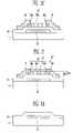
- FIG. 1is a cross-sectional view illustrating a thin film transistor (TFT), according to an exemplary embodiment of the present invention
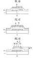
- FIGS. 2A to 2Care cross-sectional views sequentially illustrating a method of fabricating the TFT of FIG. 1 ;
- FIG. 3is a cross-sectional view illustrating a TFT, according to another exemplary embodiment of the present invention.
- FIGS. 4A to 4Eare cross-sectional views sequentially illustrating a method of fabricating the TFT of FIG. 3 ;
- FIGS. 5A and 5Bare cross-sectional views illustrating TFTs, according to still other exemplary embodiments of the present invention.
- FIG. 6is a graph illustrating the resistances R T of active layers according to length L, of a conventional TFT and an exemplary TFT, and
- FIG. 7is a graph illustrating drain currents Id according to gate voltages Vg, of the conventional TFT and the exemplary TFT.
- FIG. 1is a cross-sectional view illustrating a thin film transistor (TFT) 10 , according to an exemplary embodiment of the present invention.
- the TFT 10has a bottom gate structure (an inverse staggered structure) and includes a substrate 1 , a gate electrode 12 formed on the substrate 1 , a gate insulating layer 14 formed on the gate electrode 12 and the substrate 1 , an active layer 16 formed on the gate insulating layer 14 and disposed over the gate electrode 12 , and source and drain electrodes 18 formed on contact regions 16 a of the active layer 16 .
- the active layer 16can include an oxide semiconductor, for example, an amorphous oxide having electron carriers with a density of less than 1018/cm 3 .
- the active layer 16can reduce the leakage current of the TFT 10 , improve the switching characteristics (increase the on-off ratio), and improve the saturation current and switching speed in a pinch-off state.
- the active layer 16can be disposed so as to overlap the gate electrode 12 .
- the amorphous oxidecan include indium (In), zinc (Zn), and tin (Sn); In, Zn, and gallium (Ga), or a combination thereof.
- the active layer 16can include In—Ga—Zn—O (IGZO), which can be represented as InGaO 3 (ZnO) m (m is a natural number less than 6) in a crystalline state.
- IGZOIn—Ga—Zn—O
- ZnOInGaO 3
- mis a natural number less than 6
- the active layer 16can include In—Ga—Zn—Mg—O (IGZMO), which can be represented as InGaO 3 (Zn1-XMg x O) m (0 ⁇ X ⁇ 1 and m is a natural number less than 6) containing an electron carrier having a density of less than 1 ⁇ 1018/cm 3 .
- the active layer 16can include an amorphous oxide containing at least one of Li, Na, Mn, Ni, Pd, Cu, Cd, C, N, P, Ti, Zr, Hf, V, Ru, Ge, Sn, and F.
- the thickness d 2 of the contact portions 16 ais less than the thickness d 1 of the remaining region 16 b . Therefore, the contact resistance between the active layer 16 and the source and drain electrodes 18 is reduced.
- the remaining region 16 brefers to all areas of the active layer 16 , except for the contact portions 16 a .
- the source and drain electrodes 18can be disposed so as to contact the contact regions.
- the total resistance R T of the active layer 16is the sum of the channel resistance R Ch generated by a channel unit and the contact resistance R C generated by the contact between the active layer 16 and the source and drain electrodes 18 .
- the contact resistance R Cshould ideally be 0.
- the contact resistance R Cis a parasitic resistance between the active layer 16 and the source and drain electrodes 18 .
- the contact resistance R Cis the sum of an injection resistance Ri and an access resistance Ra.
- the injection resistance Riis related to the material characteristics of the active layer 16 and the source and drain electrodes 18 .
- the access resistance Rais related to the thickness d 2 of the contact regions 16 a.
- the thickness d 2 of the contact regions 16 ais reduced, to decrease the contact resistance R C and improve the performance of the TFT 10 .
- the thickness d 2 of the regions 16 acan be 10% to 90% of the thickness d 1 of the remaining region 16 b . This is because it is may be difficult to pattern the active layer, such that the thickness d 2 is less than 10% of the thickness d 1 . If the thickness d 2 of the contact regions 16 a is greater than 90% of the thickness d 1 of the remaining region 16 b , the contact resistance R C may not be significantly reduced.
- the characteristics of the TFT 10are improved, because the active layer 16 is formed of the oxide semiconductor, as compared with a TFT having an amorphous silicon (a-Si), or a polysilicon (poly-Si), active layer.
- the TFT 10does not require an additional crystallizing process to crystallize the active layer 16 , which is the case when using a low temperature polysilicon (LTPS) active layer.
- the active material layer 16can be formed by sputtering and can be easily enlarged using current equipment.
- the thickness d 2 of the contact regions 16 ais smaller than the thickness d 1 of the remaining region 16 b , which reduces the contact resistance Rc and improves the performance of the TFT 10 . Furthermore, since the thickness d 2 is locally reduced, it is possible to stably form the TFT 10 .
- the active layer 16includes the oxide semiconductor.
- the present inventionis not so limited.
- the active layer 16can be formed of amorphous silicon (a-Si) or polysilicon (poly-Si). In such a case, it is possible to reduce the contact resistance Rc, by locally reducing the thickness d 2 of the contact regions 16 a.
- FIGS. 2A to 2Care cross-sectional views sequentially illustrating a method of fabricating the TFT 10 of FIG. 1 .
- the gate electrode 12 and the gate insulating layer 14are sequentially formed on the substrate 1 ( FIG. 2A ).
- an oxide semiconductor layeris formed on the gate insulating layer 14 and then patterned to form the active layer 16 .
- the active layer 16is formed using a half-tone mask, so that the thickness d 2 of the contact regions 16 a is reduced, with respect to the thickness d 1 of the remaining region 16 b .
- the thickness d 2can be from about 10% to 90% of the thickness d 1 ( FIG. 2B ).
- the source and drain electrodes 18are formed on the contact regions 16 a ( FIG. 2C ).
- the thickness of the contact regions 16 acan be locally reduced.
- FIG. 3is a cross-sectional view illustrating a TFT 10 ′, according to another exemplary embodiment of the present invention. Elements similar to the elements of FIG. 2 have the same reference numerals, and a detailed description thereof is omitted.
- the TFT 10 ′includes an etch stop layer 19 formed on a remaining region 16 b of an active layer 16 , but is not formed on contact regions 16 a thereof, which contact source and drain electrodes 18 .
- the etch stop layer 19can be formed of various insulating materials and can be a passivation layer that protects the active layer 16 .
- FIGS. 4A to 4Eare cross-sectional views sequentially illustrating a method of fabricating the TFT 10 ′ of FIG. 3 .
- a gate electrode 12 and a gate insulating layer 14are sequentially formed on a substrate 1 ( FIG. 4A ).
- an active material layer 16which is formed of an oxide semiconductor, is formed on the gate insulating layer 14 .
- the active material layer 16can initially have a uniform thickness ( FIG. 4B ).
- an etch stop material 19 ais formed on the active layer 16 , in order to protect the active layer 16 from damage during subsequent processes ( FIG. 4C ).
- the etch stop layer 19is etched using a patterning process, to expose contact regions 16 a , but is not removed from a remaining region 16 b .
- an over-etching processis performed, such as dry etching or wet etching, using an etching solution with a small selection ratio.
- the over-etchingreduces the thickness of the contact regions 16 a .
- the over-etchingcan be performed so that the thickness d 2 of the contact regions 16 a is from about 10% to 90% of the thickness d 1 of the remaining region 16 b . Therefore, the patterning results in the active layer 16 having a stepped structure ( FIG. 4D ).
- the source and drain electrodes 18are formed on the contact regions 16 a ( FIG. 4E ).
- the thickness of the active layer 16can be locally reduced in the contact regions 16 a.
- FIGS. 5A and 5Bare cross-sectional views illustrating TFTs 10 ′′ and 10′′′, according to exemplary embodiments of the present invention. Elements similar to previously described elements have the same reference numbers and are not described in detail. Referring to FIGS. 5A and 5B , TFTs 10 ′′ and 10′′′ include an interface stabilizing layer 15 disposed under an active layer 16 .
- the interface stabilizing layer 15includes an oxide having a band gap equal to, or greater than, the band gap of the active layer 16 .
- the band gapcan be from about 3.0 eV to 8.0 eV.
- the oxidecan be selected from the group consisting of SiO x , SiN, SiO x N y , SiO x C y , SiO x C y H z , SiO x F y , GeO x , GdO x , AlO x , GaO c , SbO, ZrO x , HfO x , TaO x , YO x , VO x , MgO x , CaO x , BaO x , SrO x , and SOG (spun on glass).
- the band gap of the interface stabilizing layer 15is less than about 3.0 eV, charge can easily escape, and the carrier of a channel may not be effectively used.
- the band gapis larger than 8.0 eV, electrical characteristics may be reduced, due to highly insulating characteristics.
- the interface stabilizing layer 15is flush with the gate insulating layer 14 , a high stability interface is formed. Since the interface stabilizing layer 15 has a band gap equal to, or greater than that of the active layer 16 , charge trapping is suppressed.
- the hydrogen density of the interface stabilizing layer 15can be 10 +19 /cm 3 , or less.
- the hydrogen density of the interface stabilizing layer 15is greater than 10 +19 /cm 3 , hydrogen can diffuse into the surface of the active layer 16 and may operate as a trap, thereby reducing the electrical characteristics of the active layer 16 .
- a physical deposition methodsuch as sputtering can be used, rather than a chemical deposition method.
- the interface stabilizing layer 15can entirely cover the gate insulating layer 14 , as illustrated in FIGS. 5A and 5B , or can be patterned to correspond to only the active layer 16 .
- the interface stabilizing layer 15when it is formed of a conductive material, it can be patterned simultaneously with the active layer 16 , so as to be provided only under the active layer 16 .
- the interface stabilizing layer 15can be formed to a thickness of about 50 ⁇ to 5,000 ⁇ , so that the active layer 16 can be protected enough to maintain interface stability.
- the interface stabilizing layer 15can be disposed on the active layer 16 .
- the interface stabilizing layer 15can have a thickness of about 100 ⁇ , or less, for example, a thickness of about 10 ⁇ to 20 ⁇ , to reduce the contact resistance between the source and drain electrodes 18 and the active layer 16 .
- the interface stabilizing layer 15can be formed to correspond to the etch stop layer 19 .
- the interface stabilizing layer 15can protect the active layer 16 and can be used as an etch stop layer when etching the source and drain electrodes 18 . Therefore, an additional etch stop layer need not be provided.
- FIG. 6is a graph illustrating the total resistance R T of active layers, according to length L, of a conventional TFT and an exemplary TFT, according to aspects of the present invention.
- the conventional TFT lineshows the total resistance R T of the active layer of the conventional TFT, where the active layer was formed to have a uniform thickness of d 1 .
- the exemplary TFT lineshows the total resistance R T of the active layer of the exemplary TFT, where the thickness of contact regions of the active layer was reduced by 40%, in comparison with the thickness of the remaining region thereof.
- the R T W of the Y axisrepresents the product of the total resistance R T and the width W of the active layer (5 ⁇ m).
- the units of the X axisare [ ⁇ m] and the units of the Y axis are [Ohm ⁇ cm].
- the total resistance of the active layer of the conventional TFT and the exemplary TFTincreased linearly, in accordance with an increase in the length L.
- the contact resistance R C of the conventional TFTwas less than the contact resistance Rc of the exemplary TFT.
- the exemplary and conventional TFTswere the same, except for the thickness of the contact regions.
- the length Lwas the length of the contact regions between the source and drain electrodes, and the active material layer.
- the width Wwas the width of the active layer.
- the total resistance R T of the active layerwas the sum of the channel resistance R Ch and the contact resistance R C , as described in EQUATION 1. Since the channel resistance R Ch is proportional to the unit surface resistance R Ch′ and the length L, and is inversely proportional to the width W, the total resistance R T of the active layer is illustrated in EQUATION 2.
- Equation 2R Ch and R C are measured in Ohms, and R Ch ′ is measured in Ohm/sq. Therefore, through the graph, the R Ch ′ can be extracted from the slopes of the lines, and the R C can be extracted from the Y intercept.
- the exemplary TFThad a lower contact resistance R C than the conventional TFT.
- FIG. 7is a graph illustrating the drain currents Id of the conventional TFT and the exemplary TFT of FIG. 6 .
- Vthrepresents a threshold voltage
- Mobilityrepresents carrier mobility
- SSrepresents a voltage required for increasing the drain current Id by one order.
- the dotted linesillustrate the values measured when a voltage (Vds) between a drain and a source was 5.1V.
- the solid linesillustrate the values measured when the voltage Vds was 0.1V.
- the X axisrepresents the gate voltage Vg in volts [V] and the Y axis represents the drain current Id in amps [A].
- the drain current Idincreased more rapidly in a sub-threshold region, as compared to the conventional TFT.
- a larger drain current Idflowed when the gate voltage Vg was 30V, as compared to the conventional TFT.
- the mobility of the TFTsincreases by almost two fold.
Landscapes
- Physics & Mathematics (AREA)
- Nonlinear Science (AREA)
- Engineering & Computer Science (AREA)
- Microelectronics & Electronic Packaging (AREA)
- Mathematical Physics (AREA)
- Chemical & Material Sciences (AREA)
- Crystallography & Structural Chemistry (AREA)
- General Physics & Mathematics (AREA)
- Optics & Photonics (AREA)
- Thin Film Transistor (AREA)
- Liquid Crystal (AREA)
- Electrodes Of Semiconductors (AREA)
Abstract
Description
- This application claims the benefit of Korean Patent Application No. 2008-81772, filed on Aug. 21, 2008, in the Korean Intellectual Property Office, the disclosure of which is incorporated herein, by reference.
- 1. Field of the Invention
- Aspects of the present invention relate to a thin film transistor and a method of fabricating the same.
- 2. Description of the Related Art
- Currently, thin film transistors (TFT) are widely used as switching devices and driving circuits, which control the operation of pixels in a display device, such as an organic light emitting display (OLED) or a liquid crystal display (LCD). Therefore, research into improving the characteristics of TFTs is currently being conducted.
- Contact resistance, which is generated by contact between an active layer and source and drain electrodes of a TFT, can degrade the performance of a TFT. High contact resistance can reduce the power generated by a charge injecting unit of a TFT.
- Aspects of the present invention provide a thin film transistor (TFT) having reduced contact resistance between electrodes and an active layer, and a method of fabricating the same.
- According to aspects the present invention, there is provided a thin film transistor (TFT) including a gate electrode, an active layer, and source and drain electrodes. The active layer includes contact regions that contact the source and drain electrodes, and a remaining region that excludes the contact regions. The contact regions are thinner than the remaining region.
- According to aspects the present invention, the thickness of the contact regions can be from 10% to 90% of the thickness of the remaining region.
- According to aspects the present invention, the active layer can include an oxide semiconductor.
- According to aspects the present invention, the TFT can have a bottom gate structure. The source and drain electrodes can directly contact the contact region of the active layer.
- According to aspects the present invention, the TFT can further include an etch stop layer formed on the remaining region of the active layer.
- According to aspects the present invention, the TFT can further include an interface stabilizing layer formed under the active layer. The interface stabilizing layer can include an oxide having a band gap equal to, or larger than, the band gap of the active layer.
- According to aspects the present invention, there is provided a method of fabricating a TFT, the method including forming a gate electrode on a substrate, forming a gate insulating layer on the gate electrode, forming an active layer on the gate insulating layer, and forming source and drain electrodes on contact regions of the active layer. The contact regions are formed by patterning the active layer, such that the contact regions are thinner than a remaining region of the active layer.
- According to aspects the present invention, the forming of the active layer can include forming an oxide semiconductor layer on the gate insulating layer and patterning the oxide semiconductor using a half-tone mask, to form the active layer having the contact regions.
- According to aspects the present invention, an etch stop layer can be formed on the remaining region of the active layer, prior to forming the source and drain electrodes. The active layer can be initially formed to a uniform thickness, and the patterning of the etch stop layer can include an over etching process, which forms the contact regions.
- According to aspects the present invention, the method can further include forming an interface stabilizing layer on the gate insulating layer, and then forming the active layer thereon. The interface stabilizing layer can include an oxide having a band gap equal to, or larger than, the band gap of the active layer.
- According to aspects the present invention, the contact regions have a smaller thickness than the remaining region. Therefore, the contact resistance between the source and drain electrodes and the active layer is reduced, resulting in a TFT having improved performance.
- According to aspects the present invention, the active layer includes an oxide semiconductor, which improves the characteristics of the TFT.
- Additional aspects and/or advantages of the present invention will be set forth in part in the description which follows and, in part, will be obvious from the description, or may be learned by practice of the invention.
- These and/or other aspects and advantages of the invention will become apparent and more readily appreciated from the following description of the exemplary embodiments, taken in conjunction with the accompanying drawings, of which:
FIG. 1 is a cross-sectional view illustrating a thin film transistor (TFT), according to an exemplary embodiment of the present invention;FIGS. 2A to 2C are cross-sectional views sequentially illustrating a method of fabricating the TFT ofFIG. 1 ;FIG. 3 is a cross-sectional view illustrating a TFT, according to another exemplary embodiment of the present invention;FIGS. 4A to 4E are cross-sectional views sequentially illustrating a method of fabricating the TFT ofFIG. 3 ;FIGS. 5A and 5B are cross-sectional views illustrating TFTs, according to still other exemplary embodiments of the present invention;FIG. 6 is a graph illustrating the resistances RTof active layers according to length L, of a conventional TFT and an exemplary TFT, andFIG. 7 is a graph illustrating drain currents Id according to gate voltages Vg, of the conventional TFT and the exemplary TFT.- In the following detailed description, only certain exemplary embodiments of the present invention have been shown and described, by way of illustration. As those skilled in the art would realize, the described exemplary embodiments may be modified in various different ways, all without departing from the spirit or scope of the present invention. Accordingly, the drawings and description are to be regarded as illustrative in nature and not restrictive. In addition, when an element is referred to as being disposed “on” another element, it can be disposed directly on the other element, or one or more intervening elements interposed therebetween. When an element is referred to as being “connected to” another element, it can be directly connected to the other element, or can be indirectly connected to the other element, with one or more intervening elements interposed therebetween. Herein, like reference numerals refer to like elements throughout. The exemplary embodiments of the present invention will be described as follows, with reference to the accompanying drawings.
FIG. 1 is a cross-sectional view illustrating a thin film transistor (TFT)10, according to an exemplary embodiment of the present invention. Referring toFIG. 1 , theTFT 10 has a bottom gate structure (an inverse staggered structure) and includes a substrate1, agate electrode 12 formed on the substrate1, agate insulating layer 14 formed on thegate electrode 12 and the substrate1, anactive layer 16 formed on thegate insulating layer 14 and disposed over thegate electrode 12, and source anddrain electrodes 18 formed oncontact regions 16aof theactive layer 16.- The
active layer 16 can include an oxide semiconductor, for example, an amorphous oxide having electron carriers with a density of less than 1018/cm3. Theactive layer 16 can reduce the leakage current of theTFT 10, improve the switching characteristics (increase the on-off ratio), and improve the saturation current and switching speed in a pinch-off state. Theactive layer 16 can be disposed so as to overlap thegate electrode 12. - The amorphous oxide can include indium (In), zinc (Zn), and tin (Sn); In, Zn, and gallium (Ga), or a combination thereof. As an example, the
active layer 16 can include In—Ga—Zn—O (IGZO), which can be represented as InGaO3(ZnO)m(m is a natural number less than 6) in a crystalline state. As another example, theactive layer 16 can include In—Ga—Zn—Mg—O (IGZMO), which can be represented as InGaO3(Zn1-XMgxO)m(0<X≦1 and m is a natural number less than 6) containing an electron carrier having a density of less than 1×10¹⁸/cm3. In addition, theactive layer 16 can include an amorphous oxide containing at least one of Li, Na, Mn, Ni, Pd, Cu, Cd, C, N, P, Ti, Zr, Hf, V, Ru, Ge, Sn, and F. - In the
active layer 16, the thickness d2 of thecontact portions 16ais less than the thickness d1 of theremaining region 16b. Therefore, the contact resistance between theactive layer 16 and the source and drainelectrodes 18 is reduced. The remainingregion 16brefers to all areas of theactive layer 16, except for thecontact portions 16a. The source and drainelectrodes 18 can be disposed so as to contact the contact regions. - As illustrated in the following EQUATION 1, the total resistance RTof the
active layer 16 is the sum of the channel resistance RChgenerated by a channel unit and the contact resistance RCgenerated by the contact between theactive layer 16 and the source and drainelectrodes 18.
RT=RCh+RC(units are all [Ohm]) [EQUATION 1]- Here, the contact resistance RCshould ideally be 0. However, in actuality the contact resistance RCis a parasitic resistance between the
active layer 16 and the source and drainelectrodes 18. The contact resistance RCis the sum of an injection resistance Ri and an access resistance Ra. - The injection resistance Ri is related to the material characteristics of the
active layer 16 and the source and drainelectrodes 18. The access resistance Ra is related to the thickness d2 of thecontact regions 16a. - Therefore, according to aspects of the present invention, the thickness d2 of the
contact regions 16ais reduced, to decrease the contact resistance RCand improve the performance of theTFT 10. For example, the thickness d2 of theregions 16acan be 10% to 90% of the thickness d1 of the remainingregion 16b. This is because it is may be difficult to pattern the active layer, such that the thickness d2 is less than 10% of the thickness d1. If the thickness d2 of thecontact regions 16ais greater than 90% of the thickness d1 of the remainingregion 16b, the contact resistance RCmay not be significantly reduced. - As described above, according to aspects of the present invention, the characteristics of the
TFT 10 are improved, because theactive layer 16 is formed of the oxide semiconductor, as compared with a TFT having an amorphous silicon (a-Si), or a polysilicon (poly-Si), active layer. In addition, theTFT 10 does not require an additional crystallizing process to crystallize theactive layer 16, which is the case when using a low temperature polysilicon (LTPS) active layer. Theactive material layer 16 can be formed by sputtering and can be easily enlarged using current equipment. - The thickness d2 of the
contact regions 16ais smaller than the thickness d1 of the remainingregion 16b, which reduces the contact resistance Rc and improves the performance of theTFT 10. Furthermore, since the thickness d2 is locally reduced, it is possible to stably form theTFT 10. - In the present exemplary embodiment, the
active layer 16 includes the oxide semiconductor. However, the present invention is not so limited. For example, theactive layer 16 can be formed of amorphous silicon (a-Si) or polysilicon (poly-Si). In such a case, it is possible to reduce the contact resistance Rc, by locally reducing the thickness d2 of thecontact regions 16a. FIGS. 2A to 2C are cross-sectional views sequentially illustrating a method of fabricating theTFT 10 ofFIG. 1 . In the method, thegate electrode 12 and thegate insulating layer 14 are sequentially formed on the substrate1 (FIG. 2A ).- Then, an oxide semiconductor layer is formed on the
gate insulating layer 14 and then patterned to form theactive layer 16. Theactive layer 16 is formed using a half-tone mask, so that the thickness d2 of thecontact regions 16ais reduced, with respect to the thickness d1 of the remainingregion 16b. For example, the thickness d2 can be from about 10% to 90% of the thickness d1 (FIG. 2B ). - Then, the source and drain
electrodes 18 are formed on thecontact regions 16a(FIG. 2C ). By performing the above processes, the thickness of thecontact regions 16acan be locally reduced. FIG. 3 is a cross-sectional view illustrating aTFT 10′, according to another exemplary embodiment of the present invention. Elements similar to the elements ofFIG. 2 have the same reference numerals, and a detailed description thereof is omitted. Referring toFIG. 3 , theTFT 10′ includes anetch stop layer 19 formed on a remainingregion 16bof anactive layer 16, but is not formed oncontact regions 16athereof, which contact source and drainelectrodes 18. Theetch stop layer 19 can be formed of various insulating materials and can be a passivation layer that protects theactive layer 16.FIGS. 4A to 4E are cross-sectional views sequentially illustrating a method of fabricating theTFT 10′ ofFIG. 3 . In the method, agate electrode 12 and agate insulating layer 14 are sequentially formed on a substrate1 (FIG. 4A ).- Then, an
active material layer 16, which is formed of an oxide semiconductor, is formed on thegate insulating layer 14. Theactive material layer 16 can initially have a uniform thickness (FIG. 4B ). Then, anetch stop material 19ais formed on theactive layer 16, in order to protect theactive layer 16 from damage during subsequent processes (FIG. 4C ). - Then, the
etch stop layer 19 is etched using a patterning process, to exposecontact regions 16a, but is not removed from a remainingregion 16b. After theetch stop layer 19 is patterned, an over-etching process is performed, such as dry etching or wet etching, using an etching solution with a small selection ratio. The over-etching reduces the thickness of thecontact regions 16a. For example, the over-etching can be performed so that the thickness d2 of thecontact regions 16ais from about 10% to 90% of the thickness d1 of the remainingregion 16b. Therefore, the patterning results in theactive layer 16 having a stepped structure (FIG. 4D ). - Then, the source and drain
electrodes 18 are formed on thecontact regions 16a(FIG. 4E ). By performing the above processes the thickness of theactive layer 16 can be locally reduced in thecontact regions 16a. FIGS. 5A and 5B are cross-sectionalviews illustrating TFTs 10″ and 10′″, according to exemplary embodiments of the present invention. Elements similar to previously described elements have the same reference numbers and are not described in detail. Referring toFIGS. 5A and 5B ,TFTs 10″ and 10′″ include aninterface stabilizing layer 15 disposed under anactive layer 16.- The
interface stabilizing layer 15 includes an oxide having a band gap equal to, or greater than, the band gap of theactive layer 16. For example, the band gap can be from about 3.0 eV to 8.0 eV. The oxide can be selected from the group consisting of SiOx, SiN, SiOxNy, SiOxCy, SiOxCyHz, SiOxFy, GeOx, GdOx, AlOx, GaOc, SbO, ZrOx, HfOx, TaOx, YOx, VOx, MgOx, CaOx, BaOx, SrOx, and SOG (spun on glass). - When the band gap of the
interface stabilizing layer 15 is less than about 3.0 eV, charge can easily escape, and the carrier of a channel may not be effectively used. When the band gap is larger than 8.0 eV, electrical characteristics may be reduced, due to highly insulating characteristics. - Since the
interface stabilizing layer 15 is flush with thegate insulating layer 14, a high stability interface is formed. Since theinterface stabilizing layer 15 has a band gap equal to, or greater than that of theactive layer 16, charge trapping is suppressed. - In order to improve the charge trapping suppression, the hydrogen density of the
interface stabilizing layer 15 can be 10+19/cm3, or less. When the hydrogen density of theinterface stabilizing layer 15 is greater than 10+19/cm3, hydrogen can diffuse into the surface of theactive layer 16 and may operate as a trap, thereby reducing the electrical characteristics of theactive layer 16. In order to control the hydrogen density of theinterface stabilizing layer 15, a physical deposition method such as sputtering can be used, rather than a chemical deposition method. - The
interface stabilizing layer 15 can entirely cover thegate insulating layer 14, as illustrated inFIGS. 5A and 5B , or can be patterned to correspond to only theactive layer 16. For example, when theinterface stabilizing layer 15 is formed of a conductive material, it can be patterned simultaneously with theactive layer 16, so as to be provided only under theactive layer 16. Theinterface stabilizing layer 15 can be formed to a thickness of about 50 Å to 5,000 Å, so that theactive layer 16 can be protected enough to maintain interface stability. - As described above, when the
interface stabilizing layer 15 is disposed under theactive layer 16, a physical deposition process is performed between the process of forming thegate insulating layer 14 and the process of forming theactive layer 16. Therefore, in order to avoid redundancy, detailed description of a method of fabricating theTFT 10″ and10′″ is omitted. - Although not shown, the
interface stabilizing layer 15 can be disposed on theactive layer 16. In this case, theinterface stabilizing layer 15 can have a thickness of about 100 Å, or less, for example, a thickness of about 10 Å to 20 Å, to reduce the contact resistance between the source and drainelectrodes 18 and theactive layer 16. Theinterface stabilizing layer 15 can be formed to correspond to theetch stop layer 19. Theinterface stabilizing layer 15 can protect theactive layer 16 and can be used as an etch stop layer when etching the source and drainelectrodes 18. Therefore, an additional etch stop layer need not be provided. FIG. 6 is a graph illustrating the total resistance RTof active layers, according to length L, of a conventional TFT and an exemplary TFT, according to aspects of the present invention. InFIG. 6 , the conventional TFT line shows the total resistance RTof the active layer of the conventional TFT, where the active layer was formed to have a uniform thickness of d1. The exemplary TFT line shows the total resistance RTof the active layer of the exemplary TFT, where the thickness of contact regions of the active layer was reduced by 40%, in comparison with the thickness of the remaining region thereof. The RTW of the Y axis represents the product of the total resistance RTand the width W of the active layer (5 μm). The units of the X axis are [μm] and the units of the Y axis are [Ohm·cm].- Referring to
FIG. 6 , the total resistance of the active layer of the conventional TFT and the exemplary TFT increased linearly, in accordance with an increase in the length L. The contact resistance RCof the conventional TFT was less than the contact resistance Rc of the exemplary TFT. In the exemplary and conventional TFTs were the same, except for the thickness of the contact regions. The length L was the length of the contact regions between the source and drain electrodes, and the active material layer. The width W was the width of the active layer. - To be specific, the total resistance RTof the active layer was the sum of the channel resistance RChand the contact resistance RC, as described in EQUATION 1. Since the channel resistance RChis proportional to the unit surface resistance RCh′and the length L, and is inversely proportional to the width W, the total resistance RTof the active layer is illustrated in EQUATION 2.
RT=(RCh′/W)×L+RC [EQUATION 2]- In Equation 2, RChand RCare measured in Ohms, and RCh′ is measured in Ohm/sq. Therefore, through the graph, the RCh′ can be extracted from the slopes of the lines, and the RCcan be extracted from the Y intercept. The exemplary TFT had a lower contact resistance RCthan the conventional TFT.
FIG. 7 is a graph illustrating the drain currents Id of the conventional TFT and the exemplary TFT ofFIG. 6 . InFIG. 7 , Vth represents a threshold voltage, Mobility represents carrier mobility, and SS represents a voltage required for increasing the drain current Id by one order. The dotted lines illustrate the values measured when a voltage (Vds) between a drain and a source was 5.1V. The solid lines illustrate the values measured when the voltage Vds was 0.1V. The X axis represents the gate voltage Vg in volts [V] and the Y axis represents the drain current Id in amps [A].- Referring to
FIG. 7 , in the exemplary TFT the drain current Id increased more rapidly in a sub-threshold region, as compared to the conventional TFT. In addition, a larger drain current Id flowed when the gate voltage Vg was 30V, as compared to the conventional TFT. - According to aspects of the present invention, it is noted that the characteristics of the TFTs improved, when the thickness of the active layer is reduced in contact regions. In particular, the mobility of the TFTs increases by almost two fold.
- Although a few exemplary embodiments of the present invention have been shown and described, it would be appreciated by those skilled in the art that changes may be made in these exemplary embodiments, without departing from the principles and spirit of the invention, the scope of which is defined in the claims and their equivalents.
Claims (16)
Applications Claiming Priority (3)
| Application Number | Priority Date | Filing Date | Title |
|---|---|---|---|
| KR10-2008-0081772 | 2008-08-21 | ||
| KR1020080081772AKR20100023151A (en) | 2008-08-21 | 2008-08-21 | Thin film transistor and fabricating method thereof |
| KR2008-81772 | 2008-08-21 |
Publications (2)
| Publication Number | Publication Date |
|---|---|
| US20100044699A1true US20100044699A1 (en) | 2010-02-25 |
| US8466462B2 US8466462B2 (en) | 2013-06-18 |
Family
ID=41426343
Family Applications (1)
| Application Number | Title | Priority Date | Filing Date |
|---|---|---|---|
| US12/369,051ActiveUS8466462B2 (en) | 2008-08-21 | 2009-02-11 | Thin film transistor and method of fabricating the same |
Country Status (5)
| Country | Link |
|---|---|
| US (1) | US8466462B2 (en) |
| EP (1) | EP2157616A1 (en) |
| JP (2) | JP2010050434A (en) |
| KR (1) | KR20100023151A (en) |
| CN (1) | CN101656270A (en) |
Cited By (20)
| Publication number | Priority date | Publication date | Assignee | Title |
|---|---|---|---|---|
| US20110134142A1 (en)* | 2009-12-04 | 2011-06-09 | Semiconductor Energy Laboratory Co., Ltd. | Display device and driving method thereof |
| US20120037910A1 (en)* | 2010-08-10 | 2012-02-16 | Samsung Electronics Co., Ltd. | Display substrate and method of manufacturing the same |
| US20120104384A1 (en)* | 2010-10-29 | 2012-05-03 | Young-Joo Choi | Thin-film transistor and method for manufacturing the same |
| US20120119206A1 (en)* | 2010-11-15 | 2012-05-17 | Seong-Min Wang | Oxide Semiconductor Thin Film Transistor, and Method of Manufacturing the Same |
| US8422298B2 (en) | 2010-03-17 | 2013-04-16 | Semiconductor Energy Laboratory Co., Ltd. | Memory device and semiconductor device |
| US8440510B2 (en) | 2010-05-14 | 2013-05-14 | Semiconductor Energy Laboratory Co., Ltd. | Method for manufacturing semiconductor device |
| US8530289B2 (en) | 2010-04-23 | 2013-09-10 | Semiconductor Energy Laboratory Co., Ltd. | Method for manufacturing semiconductor device |
| US8629438B2 (en) | 2010-05-21 | 2014-01-14 | Semiconductor Energy Laboratory Co., Ltd. | Semiconductor device and manufacturing method thereof |
| US20140027763A1 (en)* | 2012-07-25 | 2014-01-30 | Innolux Corporation | Thin film transistor substrate and display device having the thin film transistor substrate |
| US8945982B2 (en) | 2010-04-23 | 2015-02-03 | Semiconductor Energy Laboratory Co., Ltd. | Manufacturing method of semiconductor device |
| US20150171114A1 (en)* | 2013-12-17 | 2015-06-18 | Samsung Display Co., Ltd. | Thin film transistor and display device using the same |
| JP2016015501A (en)* | 2010-04-02 | 2016-01-28 | 株式会社半導体エネルギー研究所 | Semiconductor device |
| US20160141426A1 (en)* | 2014-11-14 | 2016-05-19 | Innolux Corporation | Thin film transistor substrate and display panel having the thin film transistor substrate |
| US10204924B2 (en)* | 2016-01-12 | 2019-02-12 | Boe Technology Group Co., Ltd. | Thin film transistor, manufacturing method thereof, display substrate and display device |
| US20190074377A1 (en)* | 2017-09-01 | 2019-03-07 | Samsung Display Co., Ltd. | Thin film transistor and display device including the same |
| US11171245B2 (en)* | 2018-12-28 | 2021-11-09 | Lg Display Co., Ltd. | Thin film transistor comprising active layer having thickness difference and display apparatus comprising the same |
| US20210391475A1 (en)* | 2016-04-25 | 2021-12-16 | Sakai Display Products Corporation | Thin film transistor, display device, and thin film transistor manufacturing method |
| US11271085B2 (en) | 2009-12-25 | 2022-03-08 | Ricoh Company, Ltd. | Field-effect transistor having amorphous composite metal oxide insulation film, semiconductor memory, display element, image display device, and system |
| US11378611B1 (en)* | 2020-10-16 | 2022-07-05 | Changxin Memory Technologies, Inc. | Measurement method for contact resistance of transistor test device and computer-readable medium |
| US20230378369A1 (en)* | 2021-02-24 | 2023-11-23 | Taiwan Semiconductor Manufacturing Company Limited | Thin film transistor including a compositionally-modulated active region and methods for forming the same |
Families Citing this family (25)
| Publication number | Priority date | Publication date | Assignee | Title |
|---|---|---|---|---|
| KR101739154B1 (en)* | 2009-07-17 | 2017-05-23 | 가부시키가이샤 한도오따이 에네루기 켄큐쇼 | Semiconductor device and manufacturing method thereof |
| JP5899615B2 (en)* | 2010-03-18 | 2016-04-06 | 株式会社リコー | Insulating film manufacturing method and semiconductor device manufacturing method |
| JP2011187626A (en)* | 2010-03-08 | 2011-09-22 | Sony Corp | Thin film transistor and electronic apparatus |
| JP2012038924A (en)* | 2010-08-06 | 2012-02-23 | Sony Corp | Semiconductor device, display device, and electronic equipment |
| JP5655421B2 (en)* | 2010-08-06 | 2015-01-21 | ソニー株式会社 | Semiconductor device, display device, and electronic device |
| JP2012124367A (en)* | 2010-12-09 | 2012-06-28 | Lg Display Co Ltd | Oxide insulator film, oxide semiconductor thin film transistor element, and method of manufacturing the same |
| US8673426B2 (en)* | 2011-06-29 | 2014-03-18 | Semiconductor Energy Laboratory Co., Ltd. | Driver circuit, method of manufacturing the driver circuit, and display device including the driver circuit |
| US9252279B2 (en)* | 2011-08-31 | 2016-02-02 | Semiconductor Energy Laboratory Co., Ltd. | Semiconductor device and manufacturing method thereof |
| JP6045285B2 (en)* | 2011-10-24 | 2016-12-14 | 株式会社半導体エネルギー研究所 | Method for manufacturing semiconductor device |
| KR101868069B1 (en)* | 2011-11-18 | 2018-06-15 | 엘지디스플레이 주식회사 | Oxide thin film transistor and method for manufacturing the same |
| US20140027762A1 (en)* | 2012-07-27 | 2014-01-30 | Semiconductor Energy Laboratory Co. Ltd. | Semiconductor device |
| JP5991668B2 (en)* | 2012-08-23 | 2016-09-14 | 株式会社ジャパンディスプレイ | Display device and manufacturing method thereof |
| JP6264090B2 (en)* | 2013-07-31 | 2018-01-24 | 株式会社リコー | FIELD EFFECT TRANSISTOR AND METHOD FOR MANUFACTURING FIELD EFFECT TRANSISTOR |
| TWI536464B (en)* | 2014-01-15 | 2016-06-01 | 友達光電股份有限公司 | Transistor and manufacturing method thereof |
| JP6308583B2 (en)* | 2014-01-31 | 2018-04-11 | 国立研究開発法人物質・材料研究機構 | Thin film transistor, thin film transistor manufacturing method, and semiconductor device |
| JP2015185610A (en)* | 2014-03-20 | 2015-10-22 | 株式会社Joled | Thin film transistor and thin film transistor manufacturing method |
| TW201606861A (en)* | 2014-08-06 | 2016-02-16 | 中華映管股份有限公司 | Fabricating method of thin film transistor |
| CN104979380B (en)* | 2015-05-26 | 2020-08-28 | 合肥鑫晟光电科技有限公司 | A kind of thin film transistor and its manufacturing method |
| US11302717B2 (en)* | 2016-04-08 | 2022-04-12 | Semiconductor Energy Laboratory Co., Ltd. | Transistor and method for manufacturing the same |
| CN106356378B (en) | 2016-09-26 | 2023-10-27 | 合肥鑫晟光电科技有限公司 | Array substrate and manufacturing method thereof |
| US10396096B2 (en) | 2016-12-19 | 2019-08-27 | Samsung Display Co., Ltd. | Transistor array panel and manufacturing method thereof |
| CN107195549B (en)* | 2017-05-15 | 2020-07-03 | 京东方科技集团股份有限公司 | Thin film transistor, manufacturing method thereof, array substrate and display device |
| CN108598089B (en)* | 2018-04-27 | 2020-09-29 | 武汉华星光电技术有限公司 | TFT substrate manufacturing method and TFT substrate |
| CN108987468A (en)* | 2018-06-26 | 2018-12-11 | 浙江大学 | A kind of I-V race codope amorphous oxide semiconductor film and thin film transistor (TFT) |
| CN115132832A (en)* | 2022-07-29 | 2022-09-30 | 京东方科技集团股份有限公司 | Thin film transistor, array substrate, display panel and display device |
Citations (14)
| Publication number | Priority date | Publication date | Assignee | Title |
|---|---|---|---|---|
| US20020024097A1 (en)* | 2000-08-31 | 2002-02-28 | Lg. Phillips Lcd Co., Ltd. | TFT type optical detecting sensor implementing different TFTs and the fabricating method thereof |
| US20020146871A1 (en)* | 2001-04-04 | 2002-10-10 | Minoru Watanabe | Semiconductor device, method for manufacturing the same, and radiation detector |
| US20040251474A1 (en)* | 2003-01-29 | 2004-12-16 | Pioneer Corporation | Organic semiconductor element and fabrication method thereof |
| US20060244107A1 (en)* | 2003-06-20 | 2006-11-02 | Toshinori Sugihara | Semiconductor device, manufacturing method, and electronic device |
| US20060275994A1 (en)* | 2001-02-19 | 2006-12-07 | Hitachi, Ltd. | Thin film transistor, liquid crystal display and manufacturing method thereof |
| US20060286725A1 (en)* | 2005-06-16 | 2006-12-21 | Hua-Chi Cheng | Method for manufacturing thin film transistors |
| US20070026585A1 (en)* | 2005-07-28 | 2007-02-01 | Palo Alto Research Center Incorporated | Patterned-print thin-film transistors with top gate geometry |
| US20070029614A1 (en)* | 2005-08-05 | 2007-02-08 | Nec Lcd Technologies,Ltd. | Semiconductor device with thin-film transistors and method of fabricating the same |
| WO2007029584A1 (en)* | 2005-09-06 | 2007-03-15 | Canon Kabushiki Kaisha | Semiconductor device |
| US7242039B2 (en)* | 2004-03-12 | 2007-07-10 | Hewlett-Packard Development Company, L.P. | Semiconductor device |
| US20070194379A1 (en)* | 2004-03-12 | 2007-08-23 | Japan Science And Technology Agency | Amorphous Oxide And Thin Film Transistor |
| US20080299702A1 (en)* | 2007-05-28 | 2008-12-04 | Samsung Electronics Co., Ltd. | METHOD OF MANUFACTURING ZnO-BASED THIN FILM TRANSISTOR |
| US7541229B2 (en)* | 2004-07-27 | 2009-06-02 | Au Optronics Corp. | Thin film transistor and method for fabricating same |
| US20100176837A1 (en)* | 2007-05-03 | 2010-07-15 | The Regents Of The University Of California | Ultra-thin organic tft chemical sensor, making thereof, and sensing method |
Family Cites Families (22)
| Publication number | Priority date | Publication date | Assignee | Title |
|---|---|---|---|---|
| JPS6439065A (en)* | 1987-08-04 | 1989-02-09 | Nec Corp | Thin film field-effect transistor |
| DK426187A (en) | 1987-08-14 | 1989-02-15 | Superfos Emballage As | PLASTIC CONTAINER WITH LOW |
| JPS6453462A (en) | 1987-08-24 | 1989-03-01 | Matsushita Electric Industrial Co Ltd | Manufacture of thin film transistor |
| JPH0277159A (en)* | 1988-09-13 | 1990-03-16 | Sumitomo Metal Ind Ltd | thin film semiconductor device |
| JP2692914B2 (en)* | 1988-12-19 | 1997-12-17 | 三洋電機株式会社 | Method for manufacturing thin film transistor |
| JP3318384B2 (en) | 1993-02-05 | 2002-08-26 | 株式会社半導体エネルギー研究所 | Thin film transistor and manufacturing method thereof |
| KR100261268B1 (en) | 1997-12-19 | 2000-08-01 | 정선종 | Method of fabricating strain gate by lithography and electroplating |
| JP2002250934A (en)* | 2001-02-26 | 2002-09-06 | Sharp Corp | Manufacturing method of matrix substrate for liquid crystal |
| JP2002368229A (en) | 2001-04-04 | 2002-12-20 | Canon Inc | Semiconductor device, manufacturing method thereof, and radiation detection device |
| KR100803177B1 (en)* | 2001-05-14 | 2008-02-14 | 삼성전자주식회사 | Thin film transistor for liquid crystal display device and manufacturing method thereof |
| KR100574297B1 (en) | 2004-09-24 | 2006-04-27 | 한국전자통신연구원 | Field effect transistor and its manufacturing method |
| KR100838752B1 (en) | 2005-08-05 | 2008-06-19 | 엔이씨 엘씨디 테크놀로지스, 엘티디. | Semiconductor device having thin film transistor and manufacturing method thereof |
| KR101174780B1 (en) | 2005-09-14 | 2012-08-20 | 엘지디스플레이 주식회사 | Method For Fabricating Thin Film Transistor And Method For Fabricating Liquid Crystal Display Device |
| KR100786498B1 (en) | 2005-09-27 | 2007-12-17 | 삼성에스디아이 주식회사 | Transparent thin film transistor and manufacturing method thereof |
| JP5064747B2 (en)* | 2005-09-29 | 2012-10-31 | 株式会社半導体エネルギー研究所 | Semiconductor device, electrophoretic display device, display module, electronic device, and method for manufacturing semiconductor device |
| US7576394B2 (en) | 2006-02-02 | 2009-08-18 | Kochi Industrial Promotion Center | Thin film transistor including low resistance conductive thin films and manufacturing method thereof |
| JP2007250982A (en)* | 2006-03-17 | 2007-09-27 | Canon Inc | Thin film transistor and display device using oxide semiconductor |
| JP5250944B2 (en)* | 2006-04-28 | 2013-07-31 | 凸版印刷株式会社 | Structure, transmissive liquid crystal display device, semiconductor circuit manufacturing method, and transmissive liquid crystal display device manufacturing method |
| JP5305630B2 (en)* | 2006-12-05 | 2013-10-02 | キヤノン株式会社 | Manufacturing method of bottom gate type thin film transistor and manufacturing method of display device |
| WO2008069255A1 (en)* | 2006-12-05 | 2008-06-12 | Canon Kabushiki Kaisha | Method for manufacturing thin film transistor using oxide semiconductor and display apparatus |
| TWI333279B (en) | 2007-01-02 | 2010-11-11 | Au Optronics Corp | Method for manufacturing an array substrate |
| TWI627757B (en)* | 2008-07-31 | 2018-06-21 | 半導體能源研究所股份有限公司 | Semiconductor device |
- 2008
- 2008-08-21KRKR1020080081772Apatent/KR20100023151A/ennot_activeCeased
- 2009
- 2009-02-11USUS12/369,051patent/US8466462B2/enactiveActive
- 2009-03-12JPJP2009059746Apatent/JP2010050434A/enactivePending
- 2009-04-28CNCN200910136929Apatent/CN101656270A/enactivePending
- 2009-08-21EPEP09252033Apatent/EP2157616A1/ennot_activeWithdrawn
- 2013
- 2013-08-15JPJP2013168871Apatent/JP2014013913A/enactivePending
Patent Citations (16)
| Publication number | Priority date | Publication date | Assignee | Title |
|---|---|---|---|---|
| US6570197B2 (en)* | 2000-08-31 | 2003-05-27 | Lg. Philips Lcd Co., Ltd. | Optical device having sensing TGTs and switching TFTs with different active layer thickness |
| US20020024097A1 (en)* | 2000-08-31 | 2002-02-28 | Lg. Phillips Lcd Co., Ltd. | TFT type optical detecting sensor implementing different TFTs and the fabricating method thereof |
| US20060275994A1 (en)* | 2001-02-19 | 2006-12-07 | Hitachi, Ltd. | Thin film transistor, liquid crystal display and manufacturing method thereof |
| US20020146871A1 (en)* | 2001-04-04 | 2002-10-10 | Minoru Watanabe | Semiconductor device, method for manufacturing the same, and radiation detector |
| US20040251474A1 (en)* | 2003-01-29 | 2004-12-16 | Pioneer Corporation | Organic semiconductor element and fabrication method thereof |
| US20060244107A1 (en)* | 2003-06-20 | 2006-11-02 | Toshinori Sugihara | Semiconductor device, manufacturing method, and electronic device |
| US7242039B2 (en)* | 2004-03-12 | 2007-07-10 | Hewlett-Packard Development Company, L.P. | Semiconductor device |
| US20070194379A1 (en)* | 2004-03-12 | 2007-08-23 | Japan Science And Technology Agency | Amorphous Oxide And Thin Film Transistor |
| US7541229B2 (en)* | 2004-07-27 | 2009-06-02 | Au Optronics Corp. | Thin film transistor and method for fabricating same |
| US20060286725A1 (en)* | 2005-06-16 | 2006-12-21 | Hua-Chi Cheng | Method for manufacturing thin film transistors |
| US20080121884A1 (en)* | 2005-07-28 | 2008-05-29 | Palo Alto Research Center Incorporated | Patterned-Print Thin-Film Transistors with Top Gate Geometry |
| US20070026585A1 (en)* | 2005-07-28 | 2007-02-01 | Palo Alto Research Center Incorporated | Patterned-print thin-film transistors with top gate geometry |
| US20070029614A1 (en)* | 2005-08-05 | 2007-02-08 | Nec Lcd Technologies,Ltd. | Semiconductor device with thin-film transistors and method of fabricating the same |
| WO2007029584A1 (en)* | 2005-09-06 | 2007-03-15 | Canon Kabushiki Kaisha | Semiconductor device |
| US20100176837A1 (en)* | 2007-05-03 | 2010-07-15 | The Regents Of The University Of California | Ultra-thin organic tft chemical sensor, making thereof, and sensing method |
| US20080299702A1 (en)* | 2007-05-28 | 2008-12-04 | Samsung Electronics Co., Ltd. | METHOD OF MANUFACTURING ZnO-BASED THIN FILM TRANSISTOR |
Cited By (42)
| Publication number | Priority date | Publication date | Assignee | Title |
|---|---|---|---|---|
| US20110134142A1 (en)* | 2009-12-04 | 2011-06-09 | Semiconductor Energy Laboratory Co., Ltd. | Display device and driving method thereof |
| US11271085B2 (en) | 2009-12-25 | 2022-03-08 | Ricoh Company, Ltd. | Field-effect transistor having amorphous composite metal oxide insulation film, semiconductor memory, display element, image display device, and system |
| US8711623B2 (en) | 2010-03-17 | 2014-04-29 | Semicondoctor Energy Laboratory Co., Ltd. | Memory device and semiconductor device |
| US8422298B2 (en) | 2010-03-17 | 2013-04-16 | Semiconductor Energy Laboratory Co., Ltd. | Memory device and semiconductor device |
| JP2016015501A (en)* | 2010-04-02 | 2016-01-28 | 株式会社半導体エネルギー研究所 | Semiconductor device |
| US9245983B2 (en) | 2010-04-23 | 2016-01-26 | Semiconductor Energy Laboratory Co., Ltd. | Method for manufacturing semiconductor device |
| US9978878B2 (en) | 2010-04-23 | 2018-05-22 | Semiconductor Energy Laboratory Co., Ltd. | Manufacturing method of semiconductor device |
| US9390918B2 (en) | 2010-04-23 | 2016-07-12 | Semiconductor Energy Laboratory Co., Ltd. | Manufacturing method of semiconductor device |
| US8530289B2 (en) | 2010-04-23 | 2013-09-10 | Semiconductor Energy Laboratory Co., Ltd. | Method for manufacturing semiconductor device |
| US9099499B2 (en) | 2010-04-23 | 2015-08-04 | Semiconductor Energy Laboratory Co., Ltd. | Method for manufacturing semiconductor device |
| US8945982B2 (en) | 2010-04-23 | 2015-02-03 | Semiconductor Energy Laboratory Co., Ltd. | Manufacturing method of semiconductor device |
| US8669148B2 (en) | 2010-04-23 | 2014-03-11 | Semiconductor Energy Laboratory Co., Ltd. | Method for manufacturing semiconductor device |
| US8895377B2 (en) | 2010-04-23 | 2014-11-25 | Semiconductor Energy Laboratory Co., Ltd. | Method for manufacturing semiconductor device |
| US8440510B2 (en) | 2010-05-14 | 2013-05-14 | Semiconductor Energy Laboratory Co., Ltd. | Method for manufacturing semiconductor device |
| US8629438B2 (en) | 2010-05-21 | 2014-01-14 | Semiconductor Energy Laboratory Co., Ltd. | Semiconductor device and manufacturing method thereof |
| US9142648B2 (en) | 2010-05-21 | 2015-09-22 | Semiconductor Energy Laboratory Co., Ltd. | Semiconductor device and manufacturing method thereof |
| US9601602B2 (en) | 2010-05-21 | 2017-03-21 | Semiconductor Energy Laboratory Co., Ltd. | Semiconductor device and manufacturing method thereof |
| US8461585B2 (en)* | 2010-08-10 | 2013-06-11 | Samsung Display Co., Ltd. | Display substrate and method of manufacturing the same |
| US20120037910A1 (en)* | 2010-08-10 | 2012-02-16 | Samsung Electronics Co., Ltd. | Display substrate and method of manufacturing the same |
| US20120104384A1 (en)* | 2010-10-29 | 2012-05-03 | Young-Joo Choi | Thin-film transistor and method for manufacturing the same |
| US8450733B2 (en)* | 2010-11-15 | 2013-05-28 | Samsung Display Co., Ltd. | Oxide semiconductor thin film transistor, and method of manufacturing the same |
| US20120119206A1 (en)* | 2010-11-15 | 2012-05-17 | Seong-Min Wang | Oxide Semiconductor Thin Film Transistor, and Method of Manufacturing the Same |
| KR101774256B1 (en)* | 2010-11-15 | 2017-09-05 | 삼성디스플레이 주식회사 | Oxide semiconductor thin film transistor and method of manufacturing the same |
| US20140027763A1 (en)* | 2012-07-25 | 2014-01-30 | Innolux Corporation | Thin film transistor substrate and display device having the thin film transistor substrate |
| US20150171114A1 (en)* | 2013-12-17 | 2015-06-18 | Samsung Display Co., Ltd. | Thin film transistor and display device using the same |
| US20160141426A1 (en)* | 2014-11-14 | 2016-05-19 | Innolux Corporation | Thin film transistor substrate and display panel having the thin film transistor substrate |
| US9741804B2 (en)* | 2014-11-14 | 2017-08-22 | Innolux Corporation | Thin film transistor substrate and display panel having film layer with different thicknesses |
| US10204924B2 (en)* | 2016-01-12 | 2019-02-12 | Boe Technology Group Co., Ltd. | Thin film transistor, manufacturing method thereof, display substrate and display device |
| US11955559B2 (en)* | 2016-04-25 | 2024-04-09 | Sakai Display Products Corporation | Thin film transistor, display device, and thin film transistor manufacturing method |
| US20210391475A1 (en)* | 2016-04-25 | 2021-12-16 | Sakai Display Products Corporation | Thin film transistor, display device, and thin film transistor manufacturing method |
| US20190074377A1 (en)* | 2017-09-01 | 2019-03-07 | Samsung Display Co., Ltd. | Thin film transistor and display device including the same |
| US10593808B2 (en)* | 2017-09-01 | 2020-03-17 | Samsung Display Co., Ltd. | Thin film transistor and display device including the same |
| US11309429B2 (en) | 2017-09-01 | 2022-04-19 | Samsung Display Co., Ltd. | Thin film transistor and display device including the same |
| US20220238720A1 (en)* | 2017-09-01 | 2022-07-28 | Samsung Display Co., Ltd. | Thin film transistor and display device including the same |
| US12336223B2 (en)* | 2017-09-01 | 2025-06-17 | Samsung Display Co., Ltd. | Thin film transistor and display device including the same |
| US11728436B2 (en) | 2018-12-28 | 2023-08-15 | Lg Display Co., Ltd. | Thin film transistor comprising active layer having thickness difference and display apparatus comprising the same |
| US20230307548A1 (en)* | 2018-12-28 | 2023-09-28 | Lg Display Co., Ltd. | Thin film transistor comprising active layer having thickness difference and display apparatus comprising the same |
| US11171245B2 (en)* | 2018-12-28 | 2021-11-09 | Lg Display Co., Ltd. | Thin film transistor comprising active layer having thickness difference and display apparatus comprising the same |
| US12027631B2 (en)* | 2018-12-28 | 2024-07-02 | Lg Display Co., Ltd. | Thin film transistor comprising active layer having thickness difference and display apparatus comprising the same |
| US11378611B1 (en)* | 2020-10-16 | 2022-07-05 | Changxin Memory Technologies, Inc. | Measurement method for contact resistance of transistor test device and computer-readable medium |
| US20230378369A1 (en)* | 2021-02-24 | 2023-11-23 | Taiwan Semiconductor Manufacturing Company Limited | Thin film transistor including a compositionally-modulated active region and methods for forming the same |
| US12402358B2 (en)* | 2021-02-24 | 2025-08-26 | Taiwan Semiconductor Manufacturing Company Limited | Thin film transistor including a compositionally-modulated active region and methods for forming the same |
Also Published As
| Publication number | Publication date |
|---|---|
| KR20100023151A (en) | 2010-03-04 |
| CN101656270A (en) | 2010-02-24 |
| JP2014013913A (en) | 2014-01-23 |
| EP2157616A1 (en) | 2010-02-24 |
| US8466462B2 (en) | 2013-06-18 |
| JP2010050434A (en) | 2010-03-04 |
Similar Documents
| Publication | Publication Date | Title |
|---|---|---|
| US8466462B2 (en) | Thin film transistor and method of fabricating the same | |
| US12087865B2 (en) | Thin film transistor and thin film transistor array panel including the same | |
| US10192992B2 (en) | Display device | |
| US8541258B2 (en) | Thin film transistor, method of manufacturing the same and flat panel display device having the same | |
| US8148779B2 (en) | Thin film transistor, method of manufacturing the same and flat panel display device having the same | |
| US8207531B2 (en) | Thin film transistor, display device using thin film transistor, and production method of thin film transistor | |
| US10615266B2 (en) | Thin-film transistor, manufacturing method thereof, and array substrate | |
| CN101661952B (en) | Amorphous oxide semiconductor and thin film transistor using same | |
| CN103403873B (en) | offset electrode TFT structure | |
| US9859391B2 (en) | Thin film transistor, display device, and method for manufacturing thin film transistor | |
| CN103038887A (en) | Thin film semiconductor device and method for manufacturing thin film semiconductor device | |
| KR101950834B1 (en) | Oxide thin film transistor and method for fabricating the same | |
| KR20110080118A (en) | A thin film transistor having a multilayer etch stop layer and a method of manufacturing the same | |
| JP2009004582A (en) | Semiconductor device manufacturing method, display device manufacturing method, semiconductor device, and display device |
Legal Events
| Date | Code | Title | Description |
|---|---|---|---|
| AS | Assignment | Owner name:SAMSUNG MOBILE DISPLAY CO., LTD.,KOREA, REPUBLIC O Free format text:ASSIGNMENT OF ASSIGNORS INTEREST;ASSIGNORS:CHUNG, HYUN-JOONG;KIM, MIN-KYU;JEONG, JONG-HAN;AND OTHERS;REEL/FRAME:022286/0829 Effective date:20090129 Owner name:SAMSUNG MOBILE DISPLAY CO., LTD., KOREA, REPUBLIC Free format text:ASSIGNMENT OF ASSIGNORS INTEREST;ASSIGNORS:CHUNG, HYUN-JOONG;KIM, MIN-KYU;JEONG, JONG-HAN;AND OTHERS;REEL/FRAME:022286/0829 Effective date:20090129 | |
| AS | Assignment | Owner name:SAMSUNG DISPLAY CO., LTD., KOREA, REPUBLIC OF Free format text:MERGER;ASSIGNOR:SAMSUNG MOBILE DISPLAY CO., LTD.;REEL/FRAME:028868/0413 Effective date:20120702 | |
| STCF | Information on status: patent grant | Free format text:PATENTED CASE | |
| FEPP | Fee payment procedure | Free format text:PAYOR NUMBER ASSIGNED (ORIGINAL EVENT CODE: ASPN); ENTITY STATUS OF PATENT OWNER: LARGE ENTITY | |
| FPAY | Fee payment | Year of fee payment:4 | |
| MAFP | Maintenance fee payment | Free format text:PAYMENT OF MAINTENANCE FEE, 8TH YEAR, LARGE ENTITY (ORIGINAL EVENT CODE: M1552); ENTITY STATUS OF PATENT OWNER: LARGE ENTITY Year of fee payment:8 | |
| MAFP | Maintenance fee payment | Free format text:PAYMENT OF MAINTENANCE FEE, 12TH YEAR, LARGE ENTITY (ORIGINAL EVENT CODE: M1553); ENTITY STATUS OF PATENT OWNER: LARGE ENTITY Year of fee payment:12 |