US20100039729A1 - Package with integrated magnets for electromagnetically-actuated probe-storage device - Google Patents
Package with integrated magnets for electromagnetically-actuated probe-storage deviceDownload PDFInfo
- Publication number
- US20100039729A1 US20100039729A1US12/192,009US19200908AUS2010039729A1US 20100039729 A1US20100039729 A1US 20100039729A1US 19200908 AUS19200908 AUS 19200908AUS 2010039729 A1US2010039729 A1US 2010039729A1
- Authority
- US
- United States
- Prior art keywords
- magnet
- memory device
- flux plate
- package body
- cap
- Prior art date
- Legal status (The legal status is an assumption and is not a legal conclusion. Google has not performed a legal analysis and makes no representation as to the accuracy of the status listed.)
- Abandoned
Links
- 230000004907fluxEffects0.000claimsabstractdescription83
- 239000000758substrateSubstances0.000claimsabstractdescription71
- 238000001746injection mouldingMethods0.000claims6
- 238000013507mappingMethods0.000claims1
- 239000000463materialSubstances0.000description19
- 230000005291magnetic effectEffects0.000description17
- 238000000034methodMethods0.000description12
- XEEYBQQBJWHFJM-UHFFFAOYSA-NIronChemical compound[Fe]XEEYBQQBJWHFJM-UHFFFAOYSA-N0.000description8
- 238000006073displacement reactionMethods0.000description7
- 239000010410layerSubstances0.000description7
- 230000000712assemblyEffects0.000description6
- 238000000429assemblyMethods0.000description6
- 239000003302ferromagnetic materialSubstances0.000description6
- 229920000106Liquid crystal polymerPolymers0.000description5
- 239000004977Liquid-crystal polymers (LCPs)Substances0.000description5
- PXHVJJICTQNCMI-UHFFFAOYSA-NNickelChemical compound[Ni]PXHVJJICTQNCMI-UHFFFAOYSA-N0.000description4
- 239000004033plasticSubstances0.000description4
- 230000009467reductionEffects0.000description4
- 229910000831SteelInorganic materials0.000description3
- 229910045601alloyInorganic materials0.000description3
- 239000000956alloySubstances0.000description3
- 230000000295complement effectEffects0.000description3
- 238000013500data storageMethods0.000description3
- 238000000465mouldingMethods0.000description3
- 238000007789sealingMethods0.000description3
- 239000010959steelSubstances0.000description3
- 229910000640Fe alloyInorganic materials0.000description2
- 229910000990Ni alloyInorganic materials0.000description2
- 238000013459approachMethods0.000description2
- 239000000919ceramicSubstances0.000description2
- 238000004891communicationMethods0.000description2
- 230000005684electric fieldEffects0.000description2
- 238000005530etchingMethods0.000description2
- 238000000227grindingMethods0.000description2
- 229910052742ironInorganic materials0.000description2
- 238000003801millingMethods0.000description2
- 238000012986modificationMethods0.000description2
- 230000004048modificationEffects0.000description2
- 229910052759nickelInorganic materials0.000description2
- 238000006467substitution reactionMethods0.000description2
- 238000012546transferMethods0.000description2
- 230000005355Hall effectEffects0.000description1
- 239000012790adhesive layerSubstances0.000description1
- 230000003466anti-cipated effectEffects0.000description1
- 238000003491arrayMethods0.000description1
- 238000005452bendingMethods0.000description1
- 230000008901benefitEffects0.000description1
- 239000003990capacitorSubstances0.000description1
- 230000001419dependent effectEffects0.000description1
- 238000013461designMethods0.000description1
- 230000007613environmental effectEffects0.000description1
- 239000003822epoxy resinSubstances0.000description1
- 238000004519manufacturing processMethods0.000description1
- 230000013011matingEffects0.000description1
- 239000002184metalSubstances0.000description1
- 229910052751metalInorganic materials0.000description1
- 238000004806packaging method and processMethods0.000description1
- 230000002085persistent effectEffects0.000description1
- 239000012782phase change materialSubstances0.000description1
- 230000010287polarizationEffects0.000description1
- 229920000647polyepoxidePolymers0.000description1
- 229920000642polymerPolymers0.000description1
- 230000008569processEffects0.000description1
- 238000012545processingMethods0.000description1
- 239000004065semiconductorSubstances0.000description1
- 230000003068static effectEffects0.000description1
- 239000000725suspensionSubstances0.000description1
Images


Classifications
- G—PHYSICS
- G11—INFORMATION STORAGE
- G11B—INFORMATION STORAGE BASED ON RELATIVE MOVEMENT BETWEEN RECORD CARRIER AND TRANSDUCER
- G11B9/00—Recording or reproducing using a method not covered by one of the main groups G11B3/00 - G11B7/00; Record carriers therefor
- G11B9/12—Recording or reproducing using a method not covered by one of the main groups G11B3/00 - G11B7/00; Record carriers therefor using near-field interactions; Record carriers therefor
- G11B9/14—Recording or reproducing using a method not covered by one of the main groups G11B3/00 - G11B7/00; Record carriers therefor using near-field interactions; Record carriers therefor using microscopic probe means, i.e. recording or reproducing by means directly associated with the tip of a microscopic electrical probe as used in Scanning Tunneling Microscopy [STM] or Atomic Force Microscopy [AFM] for inducing physical or electrical perturbations in a recording medium; Record carriers or media specially adapted for such transducing of information
- G11B9/1418—Disposition or mounting of heads or record carriers
- G11B9/1427—Disposition or mounting of heads or record carriers with provision for moving the heads or record carriers relatively to each other or for access to indexed parts without effectively imparting a relative movement
- G11B9/1436—Disposition or mounting of heads or record carriers with provision for moving the heads or record carriers relatively to each other or for access to indexed parts without effectively imparting a relative movement with provision for moving the heads or record carriers relatively to each other
- G11B9/1454—Positioning the head or record carrier into or out of operative position or across information tracks; Alignment of the head relative to the surface of the record carrier
- B—PERFORMING OPERATIONS; TRANSPORTING
- B82—NANOTECHNOLOGY
- B82Y—SPECIFIC USES OR APPLICATIONS OF NANOSTRUCTURES; MEASUREMENT OR ANALYSIS OF NANOSTRUCTURES; MANUFACTURE OR TREATMENT OF NANOSTRUCTURES
- B82Y10/00—Nanotechnology for information processing, storage or transmission, e.g. quantum computing or single electron logic
- G—PHYSICS
- G11—INFORMATION STORAGE
- G11B—INFORMATION STORAGE BASED ON RELATIVE MOVEMENT BETWEEN RECORD CARRIER AND TRANSDUCER
- G11B9/00—Recording or reproducing using a method not covered by one of the main groups G11B3/00 - G11B7/00; Record carriers therefor
- G11B9/02—Recording or reproducing using a method not covered by one of the main groups G11B3/00 - G11B7/00; Record carriers therefor using ferroelectric record carriers; Record carriers therefor
Definitions
- FLASH memoryis commonly used as the media contained in such memory cards, and provides a readily accessible, solid-state solution to the lag time and high power consumption problems inherent in other memory devices such as hard disk drives.
- the cost per megabyteis dramatically higher than the cost per megabyte of an equivalent amount of space on a hard disk drive.
- FLASH memorystores bits in cells comprising arrays of floating-gate transistors that require significant chip surface, limiting a maximum achievable areal density. There is a need for solutions which permit higher density data storage in a consumer-friendly form factor at a reasonable cost per megabyte.
- FIG. 1is a simplified cross-sectional view of a memory device.
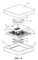
- FIG. 2is a partially exploded perspective view of the memory device of FIG. 1 and a package to house the memory device.
- FIG. 3is a simplified cross-sectional view of the memory device of FIG. 1 arranged within a package.
- FIG. 4Ais a cross-sectional view of an embodiment of a memory device and package in accordance with the present invention, wherein a portion of the support surface of the package comprises a pair of magnet assemblies.
- FIG. 4Bis a cross-sectional view of an alternative embodiment of a memory device and package in accordance with the present invention, wherein a magnet assembly is mounted within a bottom portion of the package and a magnet assembly is fixedly connected with a top portion of the package.
- FIG. 4Cis a cross-sectional view of a further embodiment of a memory device and package in accordance with the present invention, wherein a pair of magnet assemblies are mounted within corresponding components of the package.
- FIG. 4Dis a cross-sectional view of a still further embodiment of a memory device and package in accordance with the present invention, wherein a portion of the support surface of the package comprises a magnet assembly and a magnetic flux return plate.
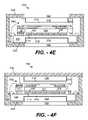
- FIG. 4Eis a cross-sectional view of a still further embodiment of a memory device and package in accordance with the present invention, wherein a portion of the support surface of the package comprises a pair of magnet assemblies, and wherein magnets of the magnet assemblies are at least partially arranged within corresponding pockets of a tip substrate and a cap.
- FIG. 4Fis a cross-sectional view of a still further embodiment of a memory device and package in accordance with the present invention, wherein a portion of the support surface of the package comprises a pair of magnet assemblies, and wherein magnets of the magnet assemblies are at least partially arranged within corresponding pockets of a tip substrate and a cap.
- FIG. 4Gis a cross-sectional view of a further embodiment of a memory device and package in accordance with the present invention, wherein the memory device comprises a single magnet assembly with a magnet of the magnet assembly at least partially arranged within corresponding pockets of a cap, and further comprising a tip substrate thinned to a reduced height.
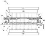
- FIG. 1is a simplified cross-sectional view of a system for storing information 100 (also referred to herein as a memory device) comprising a tip substrate 106 arranged generally parallel to a memory material or media 102 .
- the media 102is suitable for forming, removing, manipulating and/or reading indicia.
- Cantilevers 110extend from the tip substrate 106 and tips 108 extend from respective cantilevers 110 toward the media 102 .
- One or more of the tips 108is connectable with the media 102 for forming, removing, manipulating and/or reading indicia in the media 102 and/or on the surface of the media 102 .
- a media substrate 114comprises a platform 104 suspended and movable within a frame 112 by a plurality of suspension structures (e.g., flexures 112 as shown in FIG. 2 ).
- the platform 104carries the media 102 .
- the tip substrate 106is bonded to the media substrate 114 and the platform 104 (and by extension the media 102 ) is moved relative to the cantilevers 110 .
- one or both of the cantilevers 110 and the media 102can be movable to allow the tips 108 to access the media 102 .
- the memory device 100can be electrically connected with a memory device controller by way of one or more bond pads 134 .
- the platform 104 formed in the media substrate 114is movable in a Cartesian plane relative to the frame 112 by way of electromagnetic motors comprising electrical traces 132 (also referred to herein as coils, although the electrical traces need not contain turns or loops) formed on the platform 104 and placed in a magnetic field B.
- the platform 104is selectively urged in a Cartesian plane by taking advantage of Lorentz forces generated by applying current to the coils 132 while the magnetic field B is applied across the coil 132 current paths.
- the coils 132are arranged at ends of two perpendicular axes and are formed such that the media 102 is disposed between the coils 132 and the tip substrate 106 (e.g.
- the coils 132can be arranged symmetrically about a center of the platform 104 , with one pair of coils generating force for lateral (X) motion and the other pair of coils generating force for transverse (Y) motion.
- Utilization of the tip-accessible surface of the platform 104 for data storageneed not be affected by the coil layout because the coils 132 can be positioned so that the media 102 for storing indicia is disposed between the coils 132 and the tip substrate 106 , rather than co-planar with the coils 132 .
- the coilscan be formed co-planar with the surface of movable media platform. In such embodiments, a portion of the tip-accessible surface of the movable media platform will be dedicated to the coils, reducing utilization for information storage.
- the coilsneed not be arranged in a cross pattern, but rather can include fewer or more coils arranged in some other pattern.
- the magnetic field Bis generated across the platform 104 by at least one permanent magnet 120 arranged so that the permanent magnet 120 approximately maps the two perpendicular axes, the ends of which include the coils 132 .
- the permanent magnetcan have some other shape, for example the permanent magnet can be sized to approximately map the media substrate.
- the permanent magnet 120can be fixedly connected with a structure such as a flux plate 122 to form a magnet structure.
- the flux plate 122can be formed from some material suitable for containing magnetic flux, preferably a ferromagnetic material such as alloys of nickel and/or iron (e.g., steel).
- a second magnet structurecomprising a second permanent magnet 124 and a second flux plate 126 is shown and can be arranged so that the tip substrate 106 , the platform 104 , and the coils 132 are disposed between the two magnet structures.
- the magnetic fluxspans the gap between the first permanent magnet 120 and the second permanent magnet 124 .
- the second flux plate 126can be formed from some material suitable for containing magnetic flux, preferably a ferromagnetic material such as alloys of nickel and/or iron.
- a single magnet structure and a complementary flux plate without attached magnetscan be employed, where desired.
- the Lorentz force generated at the coil 132is proportional to the flux density, thus the required current and power to move the platform 104 can be increased or reduced in inverse proportion to a gap between permanent magnets 120 and 124 (assuming for the purpose of discussion that the permanent magnet type does not vary).
- a write current applied to one or more tipscould disturb the platform 104 by producing undesirable Lorentz force.
- the media 102comprises phase change material, polarity dependent material, ferroelectric material or other material requiring similar or smaller write currents to induce changes in material properties
- platform movement due to write currentsis sufficiently small as to be within track following tolerance.
- electrical trace layoutbe configured to generally negate the current applied to the tip, thereby minifying the influence of write current.
- the magnet structurecan be fixedly associated with a cap 116 that can be bonded to the frame 112 to seal the platform 104 between the tip substrate 106 and the cap 116 .
- a capacitive sensorcan comprise an electrode 138 associated with the platform 104 and one or more electrodes 140 , 142 associated with a structure held static relative to the movable media platform 104 , such as the cap 116 .
- Such devices and techniques for controlling movement of the platformare described in U.S. patent application Ser. No. 11/553,421, entitled “BONDED CHIP ASSEMBLY WITH A MICRO-MOVER FOR MICROELECTRO-MECHANICAL SYSTEMS,” filed Oct. 26, 2006 and incorporated herein by reference.
- the platform 104can rely on a pair of capacitive sensors arranged at four locations (although alternatively more or fewer locations) using each pair of capacitive sensors for extracting a ratio-metric signal independent of Z-displacement of the platform 104 .
- two electrodes 140 , 142are formed on the cap 116 .
- a third electrode 138can be integrally formed or fixedly connected with the platform 104 to form a differential pair. Two capacitors are formed, one between the first electrode 140 and third electrode 138 and one between the second electrode 142 and the third electrode 138 .
- a ratio of capacitancescan be sensitive to horizontal displacement of the platform 104 with respect to the frame 112 along an axis (X displacement) and this ratio can be insensitive to displacements of the platform 104 with respect to the frame 112 along other axes (and Z displacement).
- X displacementhorizontal displacement of the platform 104 with respect to the frame 112 along an axis
- Z displacementZ displacement
- coarse servo control of the media platform 104can be achieved using some other technique and device, such as Hall-effect sensors sensitive to magnetic field, thermal sensors to detect heat sources, etc.
- FIG. 2is a partially exploded perspective view and FIG. 3 is a simplified cross-sectional view of the memory device 100 of FIG. 1 arranged within a package 150 .
- the cap 116is shown bonded to the frame 112 , which is bonded to the tip substrate 106 , sealing the platform 104 between the cap 116 and the tip substrate 106 .
- a permanent magnet 120 and flux plate 122can be adhesively connected with a lid 156 of the package (as shown) or alternatively can be adhesively connected with the cap 116 .
- a complementary magnet structure including a second permanent magnet 124 and second flux plate 126can be fixedly connected either with a package body 152 or with the tip substrate 106 .
- the stackwhich includes the structures arranged between the two flux plates 122 , 126 , can be fixedly associated with the package 150 , for example by bonding the tip substrate 106 to the second flux plate 126 by an adhesion layer 156 .
- Lead wires 136are connected between bond pads 134 associated with the respective substrates and leads 154 that extend outside of the package 150 , allowing the memory device 100 to electrically communicate with an interface controller, a host device, or other external device.
- a gapexists between the first permanent magnet 120 and the cap 116 or between the first flux plate 122 and the lid 156 , so that some deformation of the package 150 from compressive and tensile forces can occur without unacceptably affecting tip 108 contact and/or communication with the media 102 .
- the packagemay optionally be filled with a fill material added to the cavity between the stack and the package body 152 .
- the fill materialcan be, for example, an epoxy resin for mechanically supporting the package 150 and protecting the wire bonds and memory device 100 .
- the cap 116 and first magnet structurecan be fixedly connected with the lid 156 , while a gap exists between the second magnet 124 and tip substrate 106 or second flux plate 126 and package body 152 .
- Consumer productssuch as digital cameras, cell phones, media players, and video game consoles commonly include slots for receiving and/or interfacing with memory cards.
- the slotsare typically sized and shaped, and typically include pin arrangements which complement one (or more) of several memory card form factors such as CompactFlash (CF), MultiMediaCard (MMC), Memory Stick, Secure Digital (SD), and xD.
- CFCompactFlash
- MMCMultiMediaCard
- SDSecure Digital
- xDxD
- form factor dimensionscan vary substantially, as shown below:
- a width and/or length of a stackcan be selected to conform to corresponding form factor dimensions, with constraints applied by such dimensions limiting ultimate memory capacity (by limiting media size) but not necessarily limiting the feasibility of using such a structure.
- a thickness of a memory device including a stack and magnet structuresmay approach or exceed a form factor thickness. Reducing memory device thickness may undesirably reduce one or more of magnetic flux density, structure rigidity, and package deformation tolerance.
- Embodiments of packaged memory devices and methods for fabricating such packaged memory devices in accordance with the present inventioncan be applied to reduce overall structure thickness to approach a thickness that conforms to one or more existing form factors to enable use of high density storage in host devices capable of interfacing with such form factors. Further, reduction in thickness can be achieved without unacceptably reducing magnetic flux density, structure rigidity, and package deformation tolerance.
- the first permanent magnet 120 and flux plate 122 of the device 200can be adhesively fixed to a lid 256
- the second permanent magnet 124 and flux plate 126can be integrated with a package body 252 so that the second magnet structure provides structural rigidity that is within package stress tolerances in substitution of a portion of a monolithic structure.
- the second magnet structurecan be integrated with the package body 252 using one or more of several techniques known in the art to fixedly join structures. For example, one or both of the flux plate 126 and magnet 124 can be inserted into a mold and molded by plastic (insert molded) to the package body 252 .
- the stack of tip substrate 106 , media substrate and cap 116can then be fixedly associated with the package 250 by an adhesion layer 228 bonding the stack to package body 252 and/or the magnet 124 .
- the flux plate 126 and magnet 124can be press-fit into a cavity of the package body 252 .
- the package 250(and packages described hereinafter) can be fabricated from low-thermal-expansion materials to reduce bending or distortion resulting from thermal expansion caused by environmental operating condition.
- the package body 252can be formed from a low-thermal-expansion plastic material such as liquid crystal polymer (LCP), other plastic materials, or ceramic, for example.
- the lid 256can also be formed from LCP or another polymer, a metal such as Alloy 42TM or KovarTM, or some other material known in the semiconductor packaging art.
- the coefficient of thermal expansion for LCPcan be tailored over a wide range of temperatures to minimize thermally-induced stresses. Further, LCP provides improved hermeticity to conventional plastic packages, and at a lower cost than hermetic ceramic packages. Enclosing a memory device in a sealed package enables the pressure on the memory device to be isolated, preventing unwanted deformation of the cap 116 and tip substrate 106 due to pressure mismatch between a sealed volume inside the substrate and outside atmospheric pressure.
- FIG. 4Billustrates an alternative embodiment of a memory device 200 and package 350 reduced further in thickness (and/or increased in structural rigidity) by mating the first permanent magnet 120 and first flux plate 122 with a lid 356 so that the first magnet structure provides structural rigidity that is within package stress tolerances in substitution of a portion of a monolithic structure of the lid 356 .
- the first magnet structurecan be integrated with the lid 256 by one or more of several techniques, such as insert molding, and press fitting. Integrating the first magnet structure with the lid 356 allows the lid 356 to be thickened relative to the lid 256 of FIG. 4A , to improve overall rigidity of the lid 356 while optionally reducing overall package thickness.
- the first and second magnet structures of the device 200can form at least a portion of the support surface of the package 450 .
- the magnet structurescan be integrated with the package 450 using one or more of several techniques preferably providing hermetic sealing of the package.
- one or both of the flux plate 122 , 126 and magnet 120 , 124 of the magnet structurescan be insert molded to the corresponding portion of the package.
- componentscan be press fit together, although such a technique may or may not provide a desired hermetic seal (design and fabrication tolerances may be very narrow, causing such a technique to be unreasonably costly).
- the stackcan then be fixedly associated with the package 450 by an adhesion layer 228 bonding the stack to the magnet 124 and package body 452 .
- a packaged memory devicesuch as shown in FIG. 4A can be sufficiently reduced in thickness.
- thickness of tip substrate 106 , the media substrate 112 and the cap 116can be 0.7 mm, 0.2 mm and 0.5 mm, correspondingly.
- Thickness of magnets 120 and 124can be 0.35 mm each and thickness of flux plates 122 and 126 can be 0.4 mm each.
- Thickness of adhesive layer between package 452 /magnet 124 and tip substrate 106can be 0.025 mm and gap between lid 456 /magnets 120 and the cap 116 can be as small as 0.05 mm. This brings thickness of memory device shown in FIG. 4C below 3.0 mm. Further, techniques such as insert molding can reduce assembly costs and reduce adhesion layers for which process variation can be introduced.
- FIG. 4Dillustrates a still further embodiment of a memory device 500 and package 550 resembling the embodiment of FIG. 4C and reduced further in thickness by including a single permanent magnet 120 to generate magnetic flux across the stack.
- a second flux plate 526can be insert molded to the package body 552 , or alternatively components can be press fit together.
- the stackcan then be fixedly associated with the package 550 by an adhesion layer 228 bonding the stack to the second flux plate 526 and package body 552 .
- the reduced magnetic fluxcan reduce a Lorentz force that urges the platform 104 with media 102 relative to the tip substrate 106 , which can reduce media access speeds.
- Reducing media access speedscan, for example, increase seek time, reduce a maximum read data transfer rate and/or reduce a maximum write data transfer rate.
- a reduction in magnetic fluxcan be compensated with an increase in electric field interacting with the magnetic flux.
- an increase in electric fieldmay undesirably consume power, and potentially influence polarization of domains in a ferroelectric media.
- FIG. 4Eillustrates a still further embodiment of a memory device 600 and package 650 in accordance with the present invention having two magnet structures with a reduced thickness over the embodiment of FIGS. 4A-4C .
- the first and second flux plates 122 , 126 of the first and second magnet structures of the device 600can form at least a portion of the support surface of the package 650 .
- the flux plates 122 , 126can be integrated with the package 650 using several techniques, such as insert molding and press-fitting (as above, preferably providing hermetic sealing of the package).
- one or more pockets 618can be formed in the cap 616 , for example by etching, milling, and/or grinding the exposed surface of the cap 616 .
- the pockets 618can be formed prior or subsequent to bonding of the cap 616 with the frame 112 of the media substrate.
- a gap between the cavity and the first permanent magnet 120when seated in the pockets 618 , can be sufficiently large to allow a desired amount of relative movement between the first permanent magnet 120 and the cap 616 .
- the material removed from the cap 616can generally be limited to a footprint of the first permanent magnet 120 , with allowance for the gap, so that reduction of rigidity of the cap 616 can be minimized.
- a gapwill be sufficiently large that deformation of the lid 656 of the package 650 under normal anticipated conditions of use will not apply force to the cap 616 .
- one or more pockets 619 for receiving the magnet 124can be formed in the tip substrate 606 , for example by etching, milling, and/or grinding the back surface of the tip substrate 606 .
- the material removed from the tip substrate 606can be substantially limited to a footprint of the second permanent magnet 124 so that reduction of rigidity of the tip substrate 606 can be minimized.
- the second permanent magnet 124fitted within a cavity of the tip substrate 606 can provide resistance to deformation of the tip substrate 606 where the gap substantially complements the second permanent magnet 124 .
- the media stackcan then be fixedly associated with the package 650 by an adhesion layer 628 bonding the stack to the package body 652 .
- FIG. 4Fillustrates yet another embodiment of a memory device 600 and package 750 in accordance with the present invention resembling the embodiment of FIG. 4D and having two magnet structures at least partially received within pockets 618 , 619 formed within the cap 616 and tip substrate 606 .
- the lid 756 of the materialis a monolithic structure to which a first permanent magnet 120 is bonded.
- the lid 756supplants the first flux plate by being formed of a ferromagnetic material capable of capturing magnetic flux.
- the lid 756can be formed from steel, or some other material for containing magnet flux, preferably a ferromagnetic material such as alloys containing nickel and/or iron.
- FIG. 4Gillustrates a further embodiment of a memory device 800 and package 850 in accordance with the present invention comprising a single permanent magnet 820 thinner than in previous embodiments and at least partially received within pockets 818 formed within a thinned cap 816 .
- the lid 756 of the materialis a monolithic structure to which the permanent magnet 820 is bonded.
- the lid 756supplants the first flux plate by being formed of a ferromagnetic material capable of capturing magnetic flux.
- the lid 756can be formed from steel, or some other material for containing magnet flux, preferably a ferromagnetic material such as alloys containing nickel and/or iron.
- the tip substrate 806is thinned uniformly to reduce an overall height of the stack, and bonded by an adhesion layer 228 to the package body 852 .
- the thinner and single permanent magnetgenerates a reduced magnetic flux across the coils of the electromagnetic motor.
- the memory device 800can be used with lower performance characteristics (e.g., lower seek and scan speeds), or alternatively can require increased power.
- the thinner overall height of the memory device 800may enable use in smaller form-factor memory card standards.
Landscapes
- Engineering & Computer Science (AREA)
- Chemical & Material Sciences (AREA)
- Nanotechnology (AREA)
- Physics & Mathematics (AREA)
- Mathematical Physics (AREA)
- Theoretical Computer Science (AREA)
- Crystallography & Structural Chemistry (AREA)
- Mram Or Spin Memory Techniques (AREA)
Abstract
Description
- This application incorporates by reference the following co-pending application:
- U.S. patent application Ser. No. ______, entitled “Low Distortion Package for a MEMS Device Including Memory,” Attorney Docket No. NANO-0114US0, filed concurrently.
- Software developers continue to develop steadily more data intensive products, such as ever-more sophisticated, and graphic intensive applications and operating systems (OS). Higher capacity data storage, both volatile and non-volatile, has been in persistent demand for storing code for such applications. Add to this need for capacity, the confluence of personal computing and consumer electronics in the form of personal MP3 players, such as iPod®, personal digital assistants (PDAs), sophisticated mobile phones, and laptop computers, which has placed a premium on compactness and reliability.
- Personal computing and consumer electronics commonly use memory cards that conform to one of several memory card standards that define, among other things, package form factor, pin arrangement, communication protocol, etc. FLASH memory is commonly used as the media contained in such memory cards, and provides a readily accessible, solid-state solution to the lag time and high power consumption problems inherent in other memory devices such as hard disk drives. However, the cost per megabyte is dramatically higher than the cost per megabyte of an equivalent amount of space on a hard disk drive. Further, FLASH memory stores bits in cells comprising arrays of floating-gate transistors that require significant chip surface, limiting a maximum achievable areal density. There is a need for solutions which permit higher density data storage in a consumer-friendly form factor at a reasonable cost per megabyte.
- Further details of the present invention are explained with the help of the attached drawings in which:
FIG. 1 is a simplified cross-sectional view of a memory device.FIG. 2 is a partially exploded perspective view of the memory device ofFIG. 1 and a package to house the memory device.FIG. 3 is a simplified cross-sectional view of the memory device ofFIG. 1 arranged within a package.FIG. 4A is a cross-sectional view of an embodiment of a memory device and package in accordance with the present invention, wherein a portion of the support surface of the package comprises a pair of magnet assemblies.FIG. 4B is a cross-sectional view of an alternative embodiment of a memory device and package in accordance with the present invention, wherein a magnet assembly is mounted within a bottom portion of the package and a magnet assembly is fixedly connected with a top portion of the package.FIG. 4C is a cross-sectional view of a further embodiment of a memory device and package in accordance with the present invention, wherein a pair of magnet assemblies are mounted within corresponding components of the package.FIG. 4D is a cross-sectional view of a still further embodiment of a memory device and package in accordance with the present invention, wherein a portion of the support surface of the package comprises a magnet assembly and a magnetic flux return plate.FIG. 4E is a cross-sectional view of a still further embodiment of a memory device and package in accordance with the present invention, wherein a portion of the support surface of the package comprises a pair of magnet assemblies, and wherein magnets of the magnet assemblies are at least partially arranged within corresponding pockets of a tip substrate and a cap.FIG. 4F is a cross-sectional view of a still further embodiment of a memory device and package in accordance with the present invention, wherein a portion of the support surface of the package comprises a pair of magnet assemblies, and wherein magnets of the magnet assemblies are at least partially arranged within corresponding pockets of a tip substrate and a cap.FIG. 4G is a cross-sectional view of a further embodiment of a memory device and package in accordance with the present invention, wherein the memory device comprises a single magnet assembly with a magnet of the magnet assembly at least partially arranged within corresponding pockets of a cap, and further comprising a tip substrate thinned to a reduced height.- Common reference numerals are used throughout the drawings and detailed description to indicate like elements; therefore, reference numerals used in a drawing may or may not be referenced in the detailed description specific to such drawing if the associated element is described elsewhere.
FIG. 1 is a simplified cross-sectional view of a system for storing information100 (also referred to herein as a memory device) comprising atip substrate 106 arranged generally parallel to a memory material ormedia 102. Themedia 102 is suitable for forming, removing, manipulating and/or reading indicia.Cantilevers 110 extend from thetip substrate 106 andtips 108 extend fromrespective cantilevers 110 toward themedia 102. One or more of thetips 108 is connectable with themedia 102 for forming, removing, manipulating and/or reading indicia in themedia 102 and/or on the surface of themedia 102. In the embodiment ofFIG. 1 , amedia substrate 114 comprises aplatform 104 suspended and movable within aframe 112 by a plurality of suspension structures (e.g.,flexures 112 as shown inFIG. 2 ). Theplatform 104 carries themedia 102. Thetip substrate 106 is bonded to themedia substrate 114 and the platform104 (and by extension the media102) is moved relative to thecantilevers 110. In other embodiments, one or both of thecantilevers 110 and themedia 102 can be movable to allow thetips 108 to access themedia 102. Thememory device 100 can be electrically connected with a memory device controller by way of one ormore bond pads 134.- The
platform 104 formed in themedia substrate 114 is movable in a Cartesian plane relative to theframe 112 by way of electromagnetic motors comprising electrical traces132 (also referred to herein as coils, although the electrical traces need not contain turns or loops) formed on theplatform 104 and placed in a magnetic field B. Theplatform 104 is selectively urged in a Cartesian plane by taking advantage of Lorentz forces generated by applying current to thecoils 132 while the magnetic field B is applied across thecoil 132 current paths. As shown, thecoils 132 are arranged at ends of two perpendicular axes and are formed such that themedia 102 is disposed between thecoils 132 and the tip substrate106 (e.g. fixedly connected or integrally formed with a back of theplatform 104, wherein the back is a surface of themovable media platform 104 opposite a surface contactable by tips extending from the tip substrate106). In a preferred embodiment, thecoils 132 can be arranged symmetrically about a center of theplatform 104, with one pair of coils generating force for lateral (X) motion and the other pair of coils generating force for transverse (Y) motion. Utilization of the tip-accessible surface of theplatform 104 for data storage need not be affected by the coil layout because thecoils 132 can be positioned so that themedia 102 for storing indicia is disposed between thecoils 132 and thetip substrate 106, rather than co-planar with thecoils 132. In other embodiments the coils can be formed co-planar with the surface of movable media platform. In such embodiments, a portion of the tip-accessible surface of the movable media platform will be dedicated to the coils, reducing utilization for information storage. Further, in other embodiments the coils need not be arranged in a cross pattern, but rather can include fewer or more coils arranged in some other pattern. - The magnetic field B is generated across the
platform 104 by at least onepermanent magnet 120 arranged so that thepermanent magnet 120 approximately maps the two perpendicular axes, the ends of which include thecoils 132. In other embodiments, the permanent magnet can have some other shape, for example the permanent magnet can be sized to approximately map the media substrate. Thepermanent magnet 120 can be fixedly connected with a structure such as aflux plate 122 to form a magnet structure. Theflux plate 122 can be formed from some material suitable for containing magnetic flux, preferably a ferromagnetic material such as alloys of nickel and/or iron (e.g., steel). A second magnet structure comprising a secondpermanent magnet 124 and asecond flux plate 126 is shown and can be arranged so that thetip substrate 106, theplatform 104, and thecoils 132 are disposed between the two magnet structures. The magnetic flux spans the gap between the firstpermanent magnet 120 and the secondpermanent magnet 124. As above, thesecond flux plate 126 can be formed from some material suitable for containing magnetic flux, preferably a ferromagnetic material such as alloys of nickel and/or iron. As described below, in alternative embodiments, a single magnet structure and a complementary flux plate without attached magnets can be employed, where desired. - The Lorentz force generated at the
coil 132 is proportional to the flux density, thus the required current and power to move theplatform 104 can be increased or reduced in inverse proportion to a gap betweenpermanent magnets 120 and124 (assuming for the purpose of discussion that the permanent magnet type does not vary). There is a possibility that a write current applied to one or more tips could disturb theplatform 104 by producing undesirable Lorentz force. However, where themedia 102 comprises phase change material, polarity dependent material, ferroelectric material or other material requiring similar or smaller write currents to induce changes in material properties, platform movement due to write currents is sufficiently small as to be within track following tolerance. In some embodiments, it can be desired that electrical trace layout be configured to generally negate the current applied to the tip, thereby minifying the influence of write current. The magnet structure can be fixedly associated with acap 116 that can be bonded to theframe 112 to seal theplatform 104 between thetip substrate 106 and thecap 116. - Coarse servo control of the
platform 104 within theframe 112 can be achieved through the use of capacitive sensors. Referring to the partially exploded view ofFIG. 2 , a capacitive sensor can comprise anelectrode 138 associated with theplatform 104 and one ormore electrodes movable media platform 104, such as thecap 116. Such devices and techniques for controlling movement of the platform are described in U.S. patent application Ser. No. 11/553,421, entitled “BONDED CHIP ASSEMBLY WITH A MICRO-MOVER FOR MICROELECTRO-MECHANICAL SYSTEMS,” filed Oct. 26, 2006 and incorporated herein by reference. Theplatform 104 can rely on a pair of capacitive sensors arranged at four locations (although alternatively more or fewer locations) using each pair of capacitive sensors for extracting a ratio-metric signal independent of Z-displacement of theplatform 104. Preferably, twoelectrodes cap 116. Athird electrode 138 can be integrally formed or fixedly connected with theplatform 104 to form a differential pair. Two capacitors are formed, one between thefirst electrode 140 andthird electrode 138 and one between thesecond electrode 142 and thethird electrode 138. A ratio of capacitances can be sensitive to horizontal displacement of theplatform 104 with respect to theframe 112 along an axis (X displacement) and this ratio can be insensitive to displacements of theplatform 104 with respect to theframe 112 along other axes (and Z displacement). For a pair of capacitive sensors adapted to measure motion along an axis, at least two readings can be obtained from which can be extracted displacement along the axis and rotation about a center of theplatform 104. Processing signals from all capacitive sensors allows extracting three displacement and three rotational components of the motion of theplatform 104 with respect to thecap 116. Alternatively, coarse servo control of themedia platform 104 can be achieved using some other technique and device, such as Hall-effect sensors sensitive to magnetic field, thermal sensors to detect heat sources, etc. FIG. 2 is a partially exploded perspective view andFIG. 3 is a simplified cross-sectional view of thememory device 100 ofFIG. 1 arranged within apackage 150. Thecap 116 is shown bonded to theframe 112, which is bonded to thetip substrate 106, sealing theplatform 104 between thecap 116 and thetip substrate 106. Apermanent magnet 120 andflux plate 122 can be adhesively connected with alid 156 of the package (as shown) or alternatively can be adhesively connected with thecap 116. A complementary magnet structure including a secondpermanent magnet 124 andsecond flux plate 126 can be fixedly connected either with apackage body 152 or with thetip substrate 106. The stack, which includes the structures arranged between the twoflux plates package 150, for example by bonding thetip substrate 106 to thesecond flux plate 126 by anadhesion layer 156. Leadwires 136 are connected betweenbond pads 134 associated with the respective substrates and leads154 that extend outside of thepackage 150, allowing thememory device 100 to electrically communicate with an interface controller, a host device, or other external device. Preferably, a gap exists between the firstpermanent magnet 120 and thecap 116 or between thefirst flux plate 122 and thelid 156, so that some deformation of thepackage 150 from compressive and tensile forces can occur without unacceptably affectingtip 108 contact and/or communication with themedia 102. Alternatively, the package may optionally be filled with a fill material added to the cavity between the stack and thepackage body 152. The fill material can be, for example, an epoxy resin for mechanically supporting thepackage 150 and protecting the wire bonds andmemory device 100. In still other embodiments, thecap 116 and first magnet structure can be fixedly connected with thelid 156, while a gap exists between thesecond magnet 124 andtip substrate 106 orsecond flux plate 126 andpackage body 152.- Consumer products such as digital cameras, cell phones, media players, and video game consoles commonly include slots for receiving and/or interfacing with memory cards. The slots are typically sized and shaped, and typically include pin arrangements which complement one (or more) of several memory card form factors such as CompactFlash (CF), MultiMediaCard (MMC), Memory Stick, Secure Digital (SD), and xD. It can be desirable to arrange a memory device in a package having a form factor resembling one or more of the different memory card standards to provide high density storage to consumer products. However, form factor dimensions can vary substantially, as shown below:
Width, Length, Thickness, Card mm mm mm CompactFlash, Type I 43.0 36.0 3.3 CompactFlash, Type II 43.0 36.0 5.0 SmartMedia 37.0 45.0 0.76 MMC, MMCplus 24.0 32.0 1.4 RS-MMC, MMCmobile 24.0 16.0 1.4 MMCmicro 14.0 12.0 1.1 Memory Stick Standard, PRO 21.5 50.0 2.8 Memory Stick Duo, PRO Duo, PRO-HG 20.0 31.0 1.6 Memory Stick Micro “M2” 12.5 15.0 1.2 SD 24.0 32.0 2.1 miniSD 20.0 21.5 1.4 microSD 15.0 11.0 1.0 xD 25.0 20.0 1.78 USB varies varies varies
Further, with the exception of the SmartMedia and xD formats, memory cards include a controller chip that controls reading and writing between the memory device and the host device.- A width and/or length of a stack can be selected to conform to corresponding form factor dimensions, with constraints applied by such dimensions limiting ultimate memory capacity (by limiting media size) but not necessarily limiting the feasibility of using such a structure. However, a thickness of a memory device including a stack and magnet structures may approach or exceed a form factor thickness. Reducing memory device thickness may undesirably reduce one or more of magnetic flux density, structure rigidity, and package deformation tolerance. Embodiments of packaged memory devices and methods for fabricating such packaged memory devices in accordance with the present invention can be applied to reduce overall structure thickness to approach a thickness that conforms to one or more existing form factors to enable use of high density storage in host devices capable of interfacing with such form factors. Further, reduction in thickness can be achieved without unacceptably reducing magnetic flux density, structure rigidity, and package deformation tolerance.
- Referring to
FIG. 4A , an embodiment of amemory device 200 andpackage 250 in accordance with the present invention is shown. The firstpermanent magnet 120 andflux plate 122 of thedevice 200 can be adhesively fixed to alid 256, while the secondpermanent magnet 124 andflux plate 126 can be integrated with apackage body 252 so that the second magnet structure provides structural rigidity that is within package stress tolerances in substitution of a portion of a monolithic structure. The second magnet structure can be integrated with thepackage body 252 using one or more of several techniques known in the art to fixedly join structures. For example, one or both of theflux plate 126 andmagnet 124 can be inserted into a mold and molded by plastic (insert molded) to thepackage body 252. The stack oftip substrate 106, media substrate andcap 116 can then be fixedly associated with thepackage 250 by anadhesion layer 228 bonding the stack to packagebody 252 and/or themagnet 124. Alternatively, theflux plate 126 andmagnet 124 can be press-fit into a cavity of thepackage body 252. One of ordinary skill in the art will appreciate in light of the present teaching the techniques with which the structure ofFIG. 4A can be formed. Preferably, the package250 (and packages described hereinafter) can be fabricated from low-thermal-expansion materials to reduce bending or distortion resulting from thermal expansion caused by environmental operating condition. Thepackage body 252 can be formed from a low-thermal-expansion plastic material such as liquid crystal polymer (LCP), other plastic materials, or ceramic, for example. Thelid 256 can also be formed from LCP or another polymer, a metal such as Alloy 42™ or Kovar™, or some other material known in the semiconductor packaging art. The coefficient of thermal expansion for LCP can be tailored over a wide range of temperatures to minimize thermally-induced stresses. Further, LCP provides improved hermeticity to conventional plastic packages, and at a lower cost than hermetic ceramic packages. Enclosing a memory device in a sealed package enables the pressure on the memory device to be isolated, preventing unwanted deformation of thecap 116 andtip substrate 106 due to pressure mismatch between a sealed volume inside the substrate and outside atmospheric pressure. FIG. 4B illustrates an alternative embodiment of amemory device 200 andpackage 350 reduced further in thickness (and/or increased in structural rigidity) by mating the firstpermanent magnet 120 andfirst flux plate 122 with alid 356 so that the first magnet structure provides structural rigidity that is within package stress tolerances in substitution of a portion of a monolithic structure of thelid 356. As above, the first magnet structure can be integrated with thelid 256 by one or more of several techniques, such as insert molding, and press fitting. Integrating the first magnet structure with thelid 356 allows thelid 356 to be thickened relative to thelid 256 ofFIG. 4A , to improve overall rigidity of thelid 356 while optionally reducing overall package thickness.- Referring to
FIG. 4C , a further embodiment of amemory device 200 andpackage 450 in accordance with the present invention is shown. The first and second magnet structures of thedevice 200 can form at least a portion of the support surface of thepackage 450. The magnet structures can be integrated with thepackage 450 using one or more of several techniques preferably providing hermetic sealing of the package. As above, one or both of theflux plate magnet package 450 by anadhesion layer 228 bonding the stack to themagnet 124 andpackage body 452. It is estimated that a packaged memory device such as shown inFIG. 4A can be sufficiently reduced in thickness. In particular, thickness oftip substrate 106, themedia substrate 112 and thecap 116 can be 0.7 mm, 0.2 mm and 0.5 mm, correspondingly. Thickness ofmagnets flux plates package 452/magnet 124 andtip substrate 106 can be 0.025 mm and gap betweenlid 456/magnets 120 and thecap 116 can be as small as 0.05 mm. This brings thickness of memory device shown inFIG. 4C below 3.0 mm. Further, techniques such as insert molding can reduce assembly costs and reduce adhesion layers for which process variation can be introduced. FIG. 4D illustrates a still further embodiment of amemory device 500 andpackage 550 resembling the embodiment ofFIG. 4C and reduced further in thickness by including a singlepermanent magnet 120 to generate magnetic flux across the stack. Asecond flux plate 526 can be insert molded to thepackage body 552, or alternatively components can be press fit together. The stack can then be fixedly associated with thepackage 550 by anadhesion layer 228 bonding the stack to thesecond flux plate 526 andpackage body 552. The reduced magnetic flux can reduce a Lorentz force that urges theplatform 104 withmedia 102 relative to thetip substrate 106, which can reduce media access speeds. Reducing media access speeds can, for example, increase seek time, reduce a maximum read data transfer rate and/or reduce a maximum write data transfer rate. A reduction in magnetic flux can be compensated with an increase in electric field interacting with the magnetic flux. However, an increase in electric field may undesirably consume power, and potentially influence polarization of domains in a ferroelectric media.FIG. 4E illustrates a still further embodiment of amemory device 600 andpackage 650 in accordance with the present invention having two magnet structures with a reduced thickness over the embodiment ofFIGS. 4A-4C . The first andsecond flux plates device 600 can form at least a portion of the support surface of thepackage 650. Theflux plates package 650 using several techniques, such as insert molding and press-fitting (as above, preferably providing hermetic sealing of the package). To accommodate at least a portion of a firstpermanent magnet 120, one ormore pockets 618 can be formed in thecap 616, for example by etching, milling, and/or grinding the exposed surface of thecap 616. Thepockets 618 can be formed prior or subsequent to bonding of thecap 616 with theframe 112 of the media substrate. A gap between the cavity and the firstpermanent magnet 120, when seated in thepockets 618, can be sufficiently large to allow a desired amount of relative movement between the firstpermanent magnet 120 and thecap 616. The material removed from thecap 616 can generally be limited to a footprint of the firstpermanent magnet 120, with allowance for the gap, so that reduction of rigidity of thecap 616 can be minimized. However, preferably a gap will be sufficiently large that deformation of thelid 656 of thepackage 650 under normal anticipated conditions of use will not apply force to thecap 616. Likewise, to accommodate at least a portion of a secondpermanent magnet 124, one ormore pockets 619 for receiving themagnet 124 can be formed in thetip substrate 606, for example by etching, milling, and/or grinding the back surface of thetip substrate 606. The material removed from thetip substrate 606 can be substantially limited to a footprint of the secondpermanent magnet 124 so that reduction of rigidity of thetip substrate 606 can be minimized. The secondpermanent magnet 124, fitted within a cavity of thetip substrate 606 can provide resistance to deformation of thetip substrate 606 where the gap substantially complements the secondpermanent magnet 124. The media stack can then be fixedly associated with thepackage 650 by anadhesion layer 628 bonding the stack to thepackage body 652.FIG. 4F illustrates yet another embodiment of amemory device 600 andpackage 750 in accordance with the present invention resembling the embodiment ofFIG. 4D and having two magnet structures at least partially received withinpockets cap 616 andtip substrate 606. However, in this embodiment, thelid 756 of the material is a monolithic structure to which a firstpermanent magnet 120 is bonded. Thelid 756 supplants the first flux plate by being formed of a ferromagnetic material capable of capturing magnetic flux. Thelid 756 can be formed from steel, or some other material for containing magnet flux, preferably a ferromagnetic material such as alloys containing nickel and/or iron.FIG. 4G illustrates a further embodiment of amemory device 800 andpackage 850 in accordance with the present invention comprising a singlepermanent magnet 820 thinner than in previous embodiments and at least partially received withinpockets 818 formed within a thinnedcap 816. As in the previous embodiments, thelid 756 of the material is a monolithic structure to which thepermanent magnet 820 is bonded. Thelid 756 supplants the first flux plate by being formed of a ferromagnetic material capable of capturing magnetic flux. Thelid 756 can be formed from steel, or some other material for containing magnet flux, preferably a ferromagnetic material such as alloys containing nickel and/or iron. Thetip substrate 806 is thinned uniformly to reduce an overall height of the stack, and bonded by anadhesion layer 228 to thepackage body 852. The thinner and single permanent magnet generates a reduced magnetic flux across the coils of the electromagnetic motor. As a result, thememory device 800 can be used with lower performance characteristics (e.g., lower seek and scan speeds), or alternatively can require increased power. However, the thinner overall height of thememory device 800 may enable use in smaller form-factor memory card standards.- The foregoing description of the present invention has been presented for purposes of illustration and description. It is not intended to be exhaustive or to limit the invention to the precise forms disclosed. Many modifications and variations will be apparent to practitioners skilled in this art. The embodiments were chosen and described in order to best explain the principles of the invention and its practical application, thereby enabling others skilled in the art to understand the invention for various embodiments and with various modifications as are suited to the particular use contemplated. It is intended that the scope of the invention be defined by the following claims and their equivalents.
Claims (30)
1. A packaged memory device for storing information comprising:
a stack including:
a media, and
a tip substrate having a plurality of tips extending from the tip substrate and said media being accessible to the plurality of tips;
a package lid;
a first flux plate fixedly associated with the package lid;
a package body;
a second flux plate integrated with the package body so that the second flux plate provides structural rigidity to the package body;
a permanent magnet arranged between the first flux plate and the second flux plate;
wherein the package lid forms a hermetic seal with the package body;
2. The packaged memory device ofclaim 1 , wherein the permanent magnet is a first permanent magnet fixedly connected with the first flux plate; and
further comprising a second permanent magnet fixedly connected with the second flux plate; and
wherein the first magnet substantially maps the second magnet.
3. The packaged memory device ofclaim 1 , wherein:
the stack further includes a cap;
the media is arranged between the cap and the tip substrate;
the media is movable relative to the tip substrate; and
the stack is connected with the second flux plate.
4. The packaged memory device ofclaim 2 , wherein:
the stack further includes a cap;
the media is arranged between the cap and the tip substrate; and
the media is movable relative to the tip substrate; and
the stack is connected with the second permanent magnet.
5. The packaged memory device ofclaim 1 , wherein the first flux plate is integrated with the package lid so that the first flux plate provides structural rigidity to the package lid.
6. The packaged memory device ofclaim 1 , wherein:
the permanent magnet is fixedly connected with the second flux plate and integrated with the package body so that the permanent magnet provides structural rigidity to the package body; and
the stack is fixedly connected with one or both of the permanent magnet and the package body.
7. The packaged memory device ofclaim 1 , wherein the second flux plate is integrated with the package body by injection molding.
8. The packaged memory device ofclaim 1 , wherein the second flux plate is a portion of a support surface of the package body.
9. The packaged memory device ofclaim 5 , wherein the first flux plate is integrated with the package lid by injection molding.
10. The packaged memory device ofclaim 5 , wherein the first flux plate is a portion of a support surface of the package lid.
11. The packaged memory device ofclaim 1 , wherein:
the stack further includes a cap;
the media is arranged between the cap and the tip substrate, and movable relative to the tip substrate;
the permanent magnet is fixedly connected with the second flux plate;
the tip substrate includes a cavity to receive at least a portion of the permanent magnet; and
when the stack is fixedly connected with the package body, the at least a portion of the permanent magnet is received within the cavity.
12. The packaged memory device ofclaim 2 , wherein:
the stack further includes a cap;
the cap includes a first cavity to receive at least a portion of the first permanent magnet so that a gap exists between the cap and the first permanent magnet;
the media is arranged between the cap and the tip substrate, and movable relative to the tip substrate;
the tip substrate includes a second cavity to receive at least a portion of the second permanent magnet; and
when the stack is fixedly connected with the package body, the at least a portion of the second permanent magnet is received within the cavity.
13. A packaged memory device for storing information comprising:
a stack including:
a tip substrate having a plurality of tips extending from the tip substrate;
a cap;
a media arranged between the tip substrate and cap and movable relative to the tip substrate, the media being accessible to the plurality of tips;
a package lid;
a first magnet structure fixedly connected to the package lid and including a first magnet connected with a first flux plate;
a package body connectable with the package lid to form a hermetic seal;
a second magnet structure including a second magnet connected with a second flux plate;
wherein the second flux plate is integrated with the package body so that the second flux plate provides structural rigidity to the package body; and
wherein the stack is fixedly connected to one or both of the package body and the second magnet.
14. The packaged memory device ofclaim 13 , wherein the second flux plate is integrated with the package body by injection molding.
15. The packaged memory device ofclaim 13 , wherein the second flux plate is a portion of a support surface of the package body.
16. The packaged memory device ofclaim 13 , wherein the second magnet is integrated with the package body so that the second magnet provides structural rigidity to the package body.
17. The packaged memory device ofclaim 16 , wherein the second magnet is integrated with the package body by injection molding.
18. The packaged memory device ofclaim 13 , wherein:
the tip substrate includes a cavity to receive at least a portion of the second magnet; and
when the stack is fixedly connected with the package body, the at least a portion of the second magnet is received within the cavity.
19. The packaged memory device ofclaim 13 , wherein the cap includes a first cavity to receive at least a portion of the first magnet so that a gap exists between the cap and the first magnet.
20. A packaged memory device for storing information comprising:
a stack including:
a tip substrate having a plurality of tips extending from the tip substrate;
a cap;
a media arranged between the tip substrate and cap and movable relative to the tip substrate, the media being accessible to the plurality of tips;
a first flux plate;
a package body connectable with the first flux plate to form a hermetic seal;
a magnet structure including a magnet connected with a second flux plate;
wherein the second flux plate is integrated with the package body so that the second flux plate provides structural rigidity to the package body; and
wherein the stack is fixedly connected to one or both of the package body and the second magnet.
21. The packaged memory device ofclaim 20 , wherein the second flux plate is integrated with the package body by injection molding.
22. The packaged memory device ofclaim 20 , wherein the second flux plate is a portion of a support surface of the package body.
23. The packaged memory device ofclaim 20 , wherein the magnet is integrated with the package body so that the magnet provides structural rigidity to the package body.
24. The packaged memory device ofclaim 20 , wherein the magnet is integrated with the package body by injection molding.
25. The packaged memory device ofclaim 20 , wherein:
the tip substrate includes a cavity to receive at least a portion of the magnet; and
when the stack is fixedly connected with the package body, the at least a portion of the magnet is received within the cavity.
26. The packaged memory device ofclaim 20 , wherein the magnet is a second magnet, and further comprising a first magnet fixedly connected with the first flux plate and substantially mapping the second magnet.
27. The packaged memory device ofclaim 26 , wherein the cap includes a first cavity to receive at least a portion of the first magnet so that a gap exists between the cap and the first magnet.
28. The packaged memory device ofclaim 27 , wherein:
the tip substrate includes a second cavity to receive at least a portion of the second magnet; and
when the stack is fixedly connected with the package body, the at least a portion of the second magnet is received within the second cavity.
29. A packaged memory device for storing information comprising:
a stack including:
a tip substrate having a plurality of tips extending from the tip substrate;
a cap;
a media arranged between the tip substrate and cap and movable relative to the tip substrate, the media being accessible to the plurality of tips;
a first flux plate;
a second flux plate;
a package body connected between the first flux plate and the second flux plate to form a hermetic seal;
a magnet arranged between the first and second flux plates;
wherein the stack is fixedly connected to one of the first flux plate, the second flux plate and the magnet.
30. The packaged memory device ofclaim 29 , wherein:
the magnet is fixedly connected to one of the first flux plate and the second flux plate;
and
one of the tip substrate and the cap includes a cavity to receive at least a portion of the magnet.
Priority Applications (1)
| Application Number | Priority Date | Filing Date | Title |
|---|---|---|---|
| US12/192,009US20100039729A1 (en) | 2008-08-14 | 2008-08-14 | Package with integrated magnets for electromagnetically-actuated probe-storage device |
Applications Claiming Priority (1)
| Application Number | Priority Date | Filing Date | Title |
|---|---|---|---|
| US12/192,009US20100039729A1 (en) | 2008-08-14 | 2008-08-14 | Package with integrated magnets for electromagnetically-actuated probe-storage device |
Publications (1)
| Publication Number | Publication Date |
|---|---|
| US20100039729A1true US20100039729A1 (en) | 2010-02-18 |
Family
ID=41681126
Family Applications (1)
| Application Number | Title | Priority Date | Filing Date |
|---|---|---|---|
| US12/192,009AbandonedUS20100039729A1 (en) | 2008-08-14 | 2008-08-14 | Package with integrated magnets for electromagnetically-actuated probe-storage device |
Country Status (1)
| Country | Link |
|---|---|
| US (1) | US20100039729A1 (en) |
Cited By (2)
| Publication number | Priority date | Publication date | Assignee | Title |
|---|---|---|---|---|
| US20150185247A1 (en)* | 2013-12-27 | 2015-07-02 | Feras Eid | Magnet placement for integrated sensor packages |
| US9505607B2 (en)* | 2015-03-27 | 2016-11-29 | Intel Corporation | Methods of forming sensor integrated packages and structures formed thereby |
Citations (98)
| Publication number | Priority date | Publication date | Assignee | Title |
|---|---|---|---|---|
| US4575822A (en)* | 1983-02-15 | 1986-03-11 | The Board Of Trustees Of The Leland Stanford Junior University | Method and means for data storage using tunnel current data readout |
| US4987312A (en)* | 1989-11-07 | 1991-01-22 | International Business Machines Corporation | Process for repositioning atoms on a surface using a scanning tunneling microscope |
| US5091880A (en)* | 1989-02-02 | 1992-02-25 | Olympus Optical Co., Ltd. | Memory device |
| US5097443A (en)* | 1989-03-28 | 1992-03-17 | Canon Kabushiki Kaisha | Storage medium, storage method and stored information reading method |
| US5182724A (en)* | 1989-09-07 | 1993-01-26 | Canon Kabushiki Kaisha | Information processing method and information processing device |
| US5187367A (en)* | 1990-08-14 | 1993-02-16 | Canon Kabushiki Kaisha | Cantilever type probe, scanning tunneling microscope and information processing device equipped with said probe |
| US5196701A (en)* | 1991-07-31 | 1993-03-23 | International Business Machines Corporation | High-resolution detection of material property variations |
| US5283442A (en)* | 1992-02-04 | 1994-02-01 | International Business Machines Corporation | Surface profiling using scanning force microscopy |
| US5289455A (en)* | 1990-07-25 | 1994-02-22 | Canon Kabushiki Kaisha | Information recording and/or reproducing apparatus |
| US5288999A (en)* | 1990-11-19 | 1994-02-22 | At&T Bell Laboratories | Manufacturing method including near-field optical microscopic examination of a semiconductor wafer |
| US5390161A (en)* | 1990-01-11 | 1995-02-14 | Canon Kabushiki Kaisha | Microprobe, method for producing the same, and information input and/or output apparatus utilizing the same |
| US5389475A (en)* | 1991-06-21 | 1995-02-14 | Canon Kabushiki Kaisha | Recording medium and information-erasing method |
| US5394388A (en)* | 1991-06-05 | 1995-02-28 | Canon Kabushiki Kaisha | Multiple microprobe arrays for recording and reproducing encoded information |
| US5396483A (en)* | 1989-08-10 | 1995-03-07 | Canon Kabushiki Kaisha | Recording medium having a track and electrode layer provided and recording and reproducing device and system using same |
| US5396453A (en)* | 1990-10-19 | 1995-03-07 | Canon Kabushiki Kaisha | Recording/reproducing apparatus such as a memory apparatus |
| US5398229A (en)* | 1991-10-03 | 1995-03-14 | Canon Kabushiki Kaisha | Method of manufacturing cantilever drive mechanism, method of manufacturing probe drive mechanism, cantilever drive mechanism, probe drive mechanism and electronic device which uses the same |
| US5481528A (en)* | 1992-09-25 | 1996-01-02 | Canon Kabushiki Kaisha | Information processor and method using the information processor |
| US5488602A (en)* | 1989-04-25 | 1996-01-30 | Canon Kabushiki Kaisha | Information record/reproducing apparatus and information recording medium |
| US5602820A (en)* | 1995-08-24 | 1997-02-11 | International Business Machines Corporation | Method and apparatus for mass data storage |
| US5606162A (en)* | 1991-06-13 | 1997-02-25 | British Technology Group Limited | Microprobe for surface-scanning microscopes |
| US5615143A (en)* | 1994-09-19 | 1997-03-25 | Cornell Research Foundation, Inc. | Optomechanical terabit data storage system |
| US5721721A (en)* | 1987-08-25 | 1998-02-24 | Canon Kabushiki Kaisha | Two scanning probes information recording/reproducing system with one probe to detect atomic reference location on a recording medium |
| US5856672A (en)* | 1996-08-29 | 1999-01-05 | International Business Machines Corporation | Single-crystal silicon cantilever with integral in-plane tip for use in atomic force microscope system |
| US5856967A (en)* | 1997-08-27 | 1999-01-05 | International Business Machines Corporation | Atomic force microscopy data storage system with tracking servo from lateral force-sensing cantilever |
| US5861754A (en)* | 1996-07-22 | 1999-01-19 | Hewlett-Packard Company | Position detection device |
| US5866922A (en)* | 1996-12-23 | 1999-02-02 | Motorola, Inc. | Color display with integrated semiconductor leds and organic electroluminescent devices |
| US5877497A (en)* | 1995-05-13 | 1999-03-02 | International Business Machines Corporation | Data acquisition and control apparatus for scanning probe systems |
| US5878481A (en)* | 1997-04-28 | 1999-03-09 | Headway Technologies, Inc. | Pole trimming method for fabricating a magnetic transducer structure |
| US6017618A (en)* | 1997-10-29 | 2000-01-25 | International Business Machines Corporation | Ultra high density storage media and method thereof |
| US6027951A (en)* | 1994-01-05 | 2000-02-22 | Macdonald; Noel C. | Method of making high aspect ratio probes with self-aligned control electrodes |
| USRE36603E (en)* | 1989-10-13 | 2000-03-07 | International Business Machines Corp. | Distance-controlled tunneling transducer and direct access storage unit employing the transducer |
| US6038916A (en)* | 1997-07-22 | 2000-03-21 | Digital Instruments | Method and apparatus for measuring energy dissipation by a probe during operation of an atomic force microscope |
| US6195313B1 (en)* | 1997-08-29 | 2001-02-27 | Canon Kabushiki Kaisha | Tracking mechanism and method using probes for information recording/reproducing apparatus |
| US6196061B1 (en)* | 1998-11-05 | 2001-03-06 | Nanodevices, Inc. | AFM with referenced or differential height measurement |
| US6337479B1 (en)* | 1994-07-28 | 2002-01-08 | Victor B. Kley | Object inspection and/or modification system and method |
| US6339217B1 (en)* | 1995-07-28 | 2002-01-15 | General Nanotechnology Llc | Scanning probe microscope assembly and method for making spectrophotometric, near-field, and scanning probe measurements |
| US6356524B2 (en)* | 1997-08-08 | 2002-03-12 | Sony Corporation | Method of recording/reproducing an information signal |
| US6359755B1 (en)* | 1998-07-24 | 2002-03-19 | International Business Machines Corporation | Micromechanical cantilever suspension system |
| US6504152B2 (en)* | 1997-08-27 | 2003-01-07 | Imec Vzw | Probe tip configuration and a method of fabrication thereof |
| US6507552B2 (en)* | 2000-12-01 | 2003-01-14 | Hewlett-Packard Company | AFM version of diode-and cathodoconductivity-and cathodoluminescence-based data storage media |
| US6507553B2 (en)* | 1995-07-24 | 2003-01-14 | General Nanotechnology Llc | Nanometer scale data storage device and associated positioning system |
| US6509670B2 (en)* | 2000-07-19 | 2003-01-21 | Samsung Electronics Co., Ltd. | Single stage microactuator for multidimensional actuation with multi-folded spring |
| US6515957B1 (en)* | 1999-10-06 | 2003-02-04 | International Business Machines Corporation | Ferroelectric drive for data storage |
| US6515489B2 (en)* | 2000-07-18 | 2003-02-04 | Samsung Electronics Co., Ltd. | Apparatus for sensing position of electrostatic XY-stage through time-division multiplexing |
| US6515898B2 (en)* | 2001-03-13 | 2003-02-04 | Paul Scherrer Institut (Psi) | Memory element, method for structuring a surface, and storage device |
| US6521921B2 (en)* | 1999-11-09 | 2003-02-18 | Samsung Electronics Co., Ltd | Scanning probe microscope (SPM) probe having field effect transistor channel and method of fabricating the same |
| US6522566B2 (en)* | 2000-12-01 | 2003-02-18 | Hewlett-Packard Company | System modules with atomic resolution storage memory |
| US6528785B1 (en)* | 1998-12-03 | 2003-03-04 | Daiken Chemical Co., Ltd. | Fusion-welded nanotube surface signal probe and method of attaching nanotube to probe holder |
| US6677629B1 (en)* | 1997-04-01 | 2004-01-13 | Universite De Geneve | Electric or electronic component and application as non volatile memory and device with surface acoustic waves |
| US6680808B2 (en)* | 2000-03-03 | 2004-01-20 | International Business Machines Corporation | Magnetic millipede for ultra high density magnetic storage |
| US20040016995A1 (en)* | 2002-07-25 | 2004-01-29 | Kuo Shun Meen | MEMS control chip integration |
| US6690008B2 (en)* | 2000-09-15 | 2004-02-10 | Interuniversitair Microelektronica Centrum (Imec) | Probe and method of manufacturing mounted AFM probes |
| US20040027935A1 (en)* | 2002-06-06 | 2004-02-12 | Yasuo Cho | Dielectric recording/reproducing head, dielectric recording medium unit, and dielectric recording/reproducing apparatus |
| US6692145B2 (en)* | 2001-10-31 | 2004-02-17 | Wisconsin Alumni Research Foundation | Micromachined scanning thermal probe method and apparatus |
| US20040042351A1 (en)* | 2002-07-09 | 2004-03-04 | Pioneer Corporation | Dielectric recording / reproducing head and tracking mothod |
| US6704267B2 (en)* | 2001-03-23 | 2004-03-09 | Hewlett-Packard Development Company, L.P. | Atomic resolution storage systems with enhanced magnetic field protection |
| US6854648B2 (en)* | 2001-11-23 | 2005-02-15 | Samsung Electronics Co., Ltd. | Information storage apparatus using semiconductor probe |
| US6862206B1 (en)* | 2003-12-19 | 2005-03-01 | Hewlett-Packard Development Company, L.P. | Memory module hybridizing an atomic resolution storage (ARS) memory and a magnetic memory |
| US6862925B2 (en)* | 1999-12-31 | 2005-03-08 | International Business Machines Corporation | Device for contacting and/or modifying a surface having a cantilever and a method for production of said cantilever |
| US6870751B2 (en)* | 2002-11-07 | 2005-03-22 | Hewlett-Packard Development Company, L.P. | Low-energy writing in cross-point array memory devices |
| US6982898B2 (en)* | 2002-10-15 | 2006-01-03 | Nanochip, Inc. | Molecular memory integrated circuit utilizing non-vibrating cantilevers |
| US20060003493A1 (en)* | 2004-07-02 | 2006-01-05 | Milligan Donald J | Integrated metallic contact probe storage device |
| US6985377B2 (en)* | 2002-10-15 | 2006-01-10 | Nanochip, Inc. | Phase change media for high density data storage |
| US6984862B2 (en)* | 2003-10-20 | 2006-01-10 | Hewlett-Packard Development Company, L.P. | Storage device with charge trapping structure and methods |
| US6987722B2 (en)* | 2001-07-20 | 2006-01-17 | Hewlett-Packard Development Company, L.P. | Data storage devices with wafer alignment compensation |
| US6999403B2 (en)* | 2004-04-02 | 2006-02-14 | Hewlett-Packard Development Company, L.P. | Storage device having a probe to cooperate with a storage medium to provide a variable resistance |
| US7002820B2 (en)* | 2004-06-17 | 2006-02-21 | Hewlett-Packard Development Company, L.P. | Semiconductor storage device |
| US7020064B2 (en)* | 2000-05-10 | 2006-03-28 | Samsung Electronics Co., Ltd. | Rewritable data storage using carbonaceous material and writing/reading method thereof |
| US7161875B2 (en)* | 2003-06-12 | 2007-01-09 | Hewlett-Packard Development Company, L.P. | Thermal-assisted magnetic memory storage device |
| US7164646B2 (en)* | 2004-02-19 | 2007-01-16 | Hewlett-Packard Development Company, L.P. | Storage device having a storage cell programmable to one of more than two storage states |
| US20070014047A1 (en)* | 2003-05-01 | 2007-01-18 | Yasuo Cho | Recording/reproduction head and recording/reproduction device |
| US7167434B2 (en)* | 2004-03-09 | 2007-01-23 | Hewlett-Packard Development Company, L.P. | Storage device having a probe with a first plate that cooperates with a second plate to provide a variable capacitance |
| US7167435B2 (en)* | 2004-03-09 | 2007-01-23 | Hewlett-Packard Development Company, L.P. | Storage device having a probe with plural tips |
| US7171512B2 (en)* | 2004-05-17 | 2007-01-30 | Hewlett-Packard Development Company, L.P. | Highly parallel data storage chip device |
| US7170842B2 (en)* | 2001-02-15 | 2007-01-30 | Hewlett-Packard Development Company, L.P. | Methods for conducting current between a scanned-probe and storage medium |
| US7173547B2 (en)* | 2004-03-22 | 2007-02-06 | International Business Machines Incorporated | Offset compensation in local-probe data storage devices |
| US7173314B2 (en)* | 2003-08-13 | 2007-02-06 | Hewlett-Packard Development Company, L.P. | Storage device having a probe and a storage cell with moveable parts |
| US20070030791A1 (en)* | 2005-08-05 | 2007-02-08 | Hitachi, Ltd. | Probe memory device and positioning method therefor |
| US7180847B2 (en)* | 2001-03-23 | 2007-02-20 | International Business Machines, Corporation | Apparatus and method for storing and reading high data capacities |
| US20070041233A1 (en)* | 2005-08-19 | 2007-02-22 | Seagate Technology Llc | Wake-up of ferroelectric thin films for probe storage |
| US7184388B2 (en)* | 2004-03-09 | 2007-02-27 | Hewlett-Packard Development Company, L.P. | Heating elements for a storage device |
| US20070047427A1 (en)* | 2005-08-18 | 2007-03-01 | International Business Machines Corporation | Storage device and operating method therefor |
| US7186019B2 (en)* | 2002-08-29 | 2007-03-06 | International Business Machines Corporation | Thermal movement sensor |
| US7185440B2 (en)* | 2005-07-18 | 2007-03-06 | Seagate Technology Llc | Sensing contact probe |
| US7315505B2 (en)* | 2003-07-14 | 2008-01-01 | Hewlett-Packard Development Company, L.P. | Storage device having a probe with plural tips |
| US20080001075A1 (en)* | 2006-06-15 | 2008-01-03 | Nanochip, Inc. | Memory stage for a probe storage device |
| US20080017609A1 (en)* | 2004-06-04 | 2008-01-24 | Hirokazu Takahashi | Probe Head Manufacturing Method |
| US20080024910A1 (en)* | 2006-07-25 | 2008-01-31 | Seagate Technology Llc | Electric field assisted writing using a multiferroic recording media |
| US20080023885A1 (en)* | 2006-06-15 | 2008-01-31 | Nanochip, Inc. | Method for forming a nano-imprint lithography template having very high feature counts |
| US7328446B2 (en)* | 2001-09-04 | 2008-02-05 | International Business Machines Corporation | Apparatus for reducing sensitivity of an article to mechanical shock |
| US7336524B2 (en)* | 2002-10-15 | 2008-02-26 | Nanochip, Inc. | Atomic probes and media for high density data storage |
| US7336591B2 (en)* | 2003-07-28 | 2008-02-26 | International Business Machines Corporation | Data storage medium |
| US7336590B2 (en)* | 2002-09-11 | 2008-02-26 | Yasuo Cho | Dielectric reproducing apparatus, dielectric recording apparatus, and dielectric recording/reproducing apparatus |
| US20080052601A1 (en)* | 2003-09-26 | 2008-02-28 | International Business Machines Corporation | Writing and reading of data in probe-based data storage devices |
| US7474602B2 (en)* | 2003-06-19 | 2009-01-06 | International Business Machines Corporation | Data storage device comprising write head with carbon element |
| US7483363B2 (en)* | 2004-10-14 | 2009-01-27 | International Business Machines Corporation | Data storage device and method for operating a data storage device |
| US7482826B2 (en)* | 2005-01-13 | 2009-01-27 | International Business Machines Corporation | Probe for scanning over a substrate and a data storage device |
| US7489618B2 (en)* | 2003-05-22 | 2009-02-10 | Samsung Electronics Co., Ltd. | Position detection system of probe-based data storage apparatus and position detection method |
- 2008
- 2008-08-14USUS12/192,009patent/US20100039729A1/ennot_activeAbandoned
Patent Citations (99)
| Publication number | Priority date | Publication date | Assignee | Title |
|---|---|---|---|---|
| US4575822A (en)* | 1983-02-15 | 1986-03-11 | The Board Of Trustees Of The Leland Stanford Junior University | Method and means for data storage using tunnel current data readout |
| US5721721A (en)* | 1987-08-25 | 1998-02-24 | Canon Kabushiki Kaisha | Two scanning probes information recording/reproducing system with one probe to detect atomic reference location on a recording medium |
| US5091880A (en)* | 1989-02-02 | 1992-02-25 | Olympus Optical Co., Ltd. | Memory device |
| US5097443A (en)* | 1989-03-28 | 1992-03-17 | Canon Kabushiki Kaisha | Storage medium, storage method and stored information reading method |
| US5488602A (en)* | 1989-04-25 | 1996-01-30 | Canon Kabushiki Kaisha | Information record/reproducing apparatus and information recording medium |
| US5396483A (en)* | 1989-08-10 | 1995-03-07 | Canon Kabushiki Kaisha | Recording medium having a track and electrode layer provided and recording and reproducing device and system using same |
| US5182724A (en)* | 1989-09-07 | 1993-01-26 | Canon Kabushiki Kaisha | Information processing method and information processing device |
| USRE36603E (en)* | 1989-10-13 | 2000-03-07 | International Business Machines Corp. | Distance-controlled tunneling transducer and direct access storage unit employing the transducer |
| US4987312A (en)* | 1989-11-07 | 1991-01-22 | International Business Machines Corporation | Process for repositioning atoms on a surface using a scanning tunneling microscope |
| US5390161A (en)* | 1990-01-11 | 1995-02-14 | Canon Kabushiki Kaisha | Microprobe, method for producing the same, and information input and/or output apparatus utilizing the same |
| US5289455A (en)* | 1990-07-25 | 1994-02-22 | Canon Kabushiki Kaisha | Information recording and/or reproducing apparatus |
| US5187367A (en)* | 1990-08-14 | 1993-02-16 | Canon Kabushiki Kaisha | Cantilever type probe, scanning tunneling microscope and information processing device equipped with said probe |
| US5396453A (en)* | 1990-10-19 | 1995-03-07 | Canon Kabushiki Kaisha | Recording/reproducing apparatus such as a memory apparatus |
| US5288999A (en)* | 1990-11-19 | 1994-02-22 | At&T Bell Laboratories | Manufacturing method including near-field optical microscopic examination of a semiconductor wafer |
| US5394388A (en)* | 1991-06-05 | 1995-02-28 | Canon Kabushiki Kaisha | Multiple microprobe arrays for recording and reproducing encoded information |
| US5606162A (en)* | 1991-06-13 | 1997-02-25 | British Technology Group Limited | Microprobe for surface-scanning microscopes |
| US5389475A (en)* | 1991-06-21 | 1995-02-14 | Canon Kabushiki Kaisha | Recording medium and information-erasing method |
| US5196701A (en)* | 1991-07-31 | 1993-03-23 | International Business Machines Corporation | High-resolution detection of material property variations |
| US5398229A (en)* | 1991-10-03 | 1995-03-14 | Canon Kabushiki Kaisha | Method of manufacturing cantilever drive mechanism, method of manufacturing probe drive mechanism, cantilever drive mechanism, probe drive mechanism and electronic device which uses the same |
| US5283442A (en)* | 1992-02-04 | 1994-02-01 | International Business Machines Corporation | Surface profiling using scanning force microscopy |
| US5481528A (en)* | 1992-09-25 | 1996-01-02 | Canon Kabushiki Kaisha | Information processor and method using the information processor |
| US6027951A (en)* | 1994-01-05 | 2000-02-22 | Macdonald; Noel C. | Method of making high aspect ratio probes with self-aligned control electrodes |
| US6337479B1 (en)* | 1994-07-28 | 2002-01-08 | Victor B. Kley | Object inspection and/or modification system and method |
| US5615143A (en)* | 1994-09-19 | 1997-03-25 | Cornell Research Foundation, Inc. | Optomechanical terabit data storage system |
| US5877497A (en)* | 1995-05-13 | 1999-03-02 | International Business Machines Corporation | Data acquisition and control apparatus for scanning probe systems |
| US6507553B2 (en)* | 1995-07-24 | 2003-01-14 | General Nanotechnology Llc | Nanometer scale data storage device and associated positioning system |
| US6339217B1 (en)* | 1995-07-28 | 2002-01-15 | General Nanotechnology Llc | Scanning probe microscope assembly and method for making spectrophotometric, near-field, and scanning probe measurements |
| US5602820A (en)* | 1995-08-24 | 1997-02-11 | International Business Machines Corporation | Method and apparatus for mass data storage |
| US5861754A (en)* | 1996-07-22 | 1999-01-19 | Hewlett-Packard Company | Position detection device |
| US5856672A (en)* | 1996-08-29 | 1999-01-05 | International Business Machines Corporation | Single-crystal silicon cantilever with integral in-plane tip for use in atomic force microscope system |
| US5866922A (en)* | 1996-12-23 | 1999-02-02 | Motorola, Inc. | Color display with integrated semiconductor leds and organic electroluminescent devices |
| US6677629B1 (en)* | 1997-04-01 | 2004-01-13 | Universite De Geneve | Electric or electronic component and application as non volatile memory and device with surface acoustic waves |
| US5878481A (en)* | 1997-04-28 | 1999-03-09 | Headway Technologies, Inc. | Pole trimming method for fabricating a magnetic transducer structure |
| US6038916A (en)* | 1997-07-22 | 2000-03-21 | Digital Instruments | Method and apparatus for measuring energy dissipation by a probe during operation of an atomic force microscope |
| US6356524B2 (en)* | 1997-08-08 | 2002-03-12 | Sony Corporation | Method of recording/reproducing an information signal |
| US5856967A (en)* | 1997-08-27 | 1999-01-05 | International Business Machines Corporation | Atomic force microscopy data storage system with tracking servo from lateral force-sensing cantilever |
| US6504152B2 (en)* | 1997-08-27 | 2003-01-07 | Imec Vzw | Probe tip configuration and a method of fabrication thereof |
| US6195313B1 (en)* | 1997-08-29 | 2001-02-27 | Canon Kabushiki Kaisha | Tracking mechanism and method using probes for information recording/reproducing apparatus |
| US6017618A (en)* | 1997-10-29 | 2000-01-25 | International Business Machines Corporation | Ultra high density storage media and method thereof |
| US6359755B1 (en)* | 1998-07-24 | 2002-03-19 | International Business Machines Corporation | Micromechanical cantilever suspension system |
| US6196061B1 (en)* | 1998-11-05 | 2001-03-06 | Nanodevices, Inc. | AFM with referenced or differential height measurement |
| US6528785B1 (en)* | 1998-12-03 | 2003-03-04 | Daiken Chemical Co., Ltd. | Fusion-welded nanotube surface signal probe and method of attaching nanotube to probe holder |
| US6515957B1 (en)* | 1999-10-06 | 2003-02-04 | International Business Machines Corporation | Ferroelectric drive for data storage |
| US6521921B2 (en)* | 1999-11-09 | 2003-02-18 | Samsung Electronics Co., Ltd | Scanning probe microscope (SPM) probe having field effect transistor channel and method of fabricating the same |
| US6862925B2 (en)* | 1999-12-31 | 2005-03-08 | International Business Machines Corporation | Device for contacting and/or modifying a surface having a cantilever and a method for production of said cantilever |
| US6680808B2 (en)* | 2000-03-03 | 2004-01-20 | International Business Machines Corporation | Magnetic millipede for ultra high density magnetic storage |
| US7020064B2 (en)* | 2000-05-10 | 2006-03-28 | Samsung Electronics Co., Ltd. | Rewritable data storage using carbonaceous material and writing/reading method thereof |
| US6515489B2 (en)* | 2000-07-18 | 2003-02-04 | Samsung Electronics Co., Ltd. | Apparatus for sensing position of electrostatic XY-stage through time-division multiplexing |
| US6509670B2 (en)* | 2000-07-19 | 2003-01-21 | Samsung Electronics Co., Ltd. | Single stage microactuator for multidimensional actuation with multi-folded spring |
| US6690008B2 (en)* | 2000-09-15 | 2004-02-10 | Interuniversitair Microelektronica Centrum (Imec) | Probe and method of manufacturing mounted AFM probes |
| US6522566B2 (en)* | 2000-12-01 | 2003-02-18 | Hewlett-Packard Company | System modules with atomic resolution storage memory |
| US6507552B2 (en)* | 2000-12-01 | 2003-01-14 | Hewlett-Packard Company | AFM version of diode-and cathodoconductivity-and cathodoluminescence-based data storage media |
| US7170842B2 (en)* | 2001-02-15 | 2007-01-30 | Hewlett-Packard Development Company, L.P. | Methods for conducting current between a scanned-probe and storage medium |
| US6515898B2 (en)* | 2001-03-13 | 2003-02-04 | Paul Scherrer Institut (Psi) | Memory element, method for structuring a surface, and storage device |
| US7180847B2 (en)* | 2001-03-23 | 2007-02-20 | International Business Machines, Corporation | Apparatus and method for storing and reading high data capacities |
| US6704267B2 (en)* | 2001-03-23 | 2004-03-09 | Hewlett-Packard Development Company, L.P. | Atomic resolution storage systems with enhanced magnetic field protection |
| US6987722B2 (en)* | 2001-07-20 | 2006-01-17 | Hewlett-Packard Development Company, L.P. | Data storage devices with wafer alignment compensation |
| US7328446B2 (en)* | 2001-09-04 | 2008-02-05 | International Business Machines Corporation | Apparatus for reducing sensitivity of an article to mechanical shock |
| US6692145B2 (en)* | 2001-10-31 | 2004-02-17 | Wisconsin Alumni Research Foundation | Micromachined scanning thermal probe method and apparatus |
| US6854648B2 (en)* | 2001-11-23 | 2005-02-15 | Samsung Electronics Co., Ltd. | Information storage apparatus using semiconductor probe |
| US20040027935A1 (en)* | 2002-06-06 | 2004-02-12 | Yasuo Cho | Dielectric recording/reproducing head, dielectric recording medium unit, and dielectric recording/reproducing apparatus |
| US20040042351A1 (en)* | 2002-07-09 | 2004-03-04 | Pioneer Corporation | Dielectric recording / reproducing head and tracking mothod |
| US20040016995A1 (en)* | 2002-07-25 | 2004-01-29 | Kuo Shun Meen | MEMS control chip integration |
| US7186019B2 (en)* | 2002-08-29 | 2007-03-06 | International Business Machines Corporation | Thermal movement sensor |
| US7336590B2 (en)* | 2002-09-11 | 2008-02-26 | Yasuo Cho | Dielectric reproducing apparatus, dielectric recording apparatus, and dielectric recording/reproducing apparatus |
| US6985377B2 (en)* | 2002-10-15 | 2006-01-10 | Nanochip, Inc. | Phase change media for high density data storage |
| US6982898B2 (en)* | 2002-10-15 | 2006-01-03 | Nanochip, Inc. | Molecular memory integrated circuit utilizing non-vibrating cantilevers |
| US7336524B2 (en)* | 2002-10-15 | 2008-02-26 | Nanochip, Inc. | Atomic probes and media for high density data storage |
| US6870751B2 (en)* | 2002-11-07 | 2005-03-22 | Hewlett-Packard Development Company, L.P. | Low-energy writing in cross-point array memory devices |
| US20070014047A1 (en)* | 2003-05-01 | 2007-01-18 | Yasuo Cho | Recording/reproduction head and recording/reproduction device |
| US7489618B2 (en)* | 2003-05-22 | 2009-02-10 | Samsung Electronics Co., Ltd. | Position detection system of probe-based data storage apparatus and position detection method |
| US7161875B2 (en)* | 2003-06-12 | 2007-01-09 | Hewlett-Packard Development Company, L.P. | Thermal-assisted magnetic memory storage device |
| US7474602B2 (en)* | 2003-06-19 | 2009-01-06 | International Business Machines Corporation | Data storage device comprising write head with carbon element |
| US7315505B2 (en)* | 2003-07-14 | 2008-01-01 | Hewlett-Packard Development Company, L.P. | Storage device having a probe with plural tips |
| US7336591B2 (en)* | 2003-07-28 | 2008-02-26 | International Business Machines Corporation | Data storage medium |
| US7173314B2 (en)* | 2003-08-13 | 2007-02-06 | Hewlett-Packard Development Company, L.P. | Storage device having a probe and a storage cell with moveable parts |
| US20080052601A1 (en)* | 2003-09-26 | 2008-02-28 | International Business Machines Corporation | Writing and reading of data in probe-based data storage devices |
| US20080052602A1 (en)* | 2003-09-26 | 2008-02-28 | International Business Machines Corporation | Writing and reading of data in probe-based data storage devices |
| US6984862B2 (en)* | 2003-10-20 | 2006-01-10 | Hewlett-Packard Development Company, L.P. | Storage device with charge trapping structure and methods |
| US6862206B1 (en)* | 2003-12-19 | 2005-03-01 | Hewlett-Packard Development Company, L.P. | Memory module hybridizing an atomic resolution storage (ARS) memory and a magnetic memory |
| US7164646B2 (en)* | 2004-02-19 | 2007-01-16 | Hewlett-Packard Development Company, L.P. | Storage device having a storage cell programmable to one of more than two storage states |
| US7167434B2 (en)* | 2004-03-09 | 2007-01-23 | Hewlett-Packard Development Company, L.P. | Storage device having a probe with a first plate that cooperates with a second plate to provide a variable capacitance |
| US7184388B2 (en)* | 2004-03-09 | 2007-02-27 | Hewlett-Packard Development Company, L.P. | Heating elements for a storage device |
| US7167435B2 (en)* | 2004-03-09 | 2007-01-23 | Hewlett-Packard Development Company, L.P. | Storage device having a probe with plural tips |
| US7173547B2 (en)* | 2004-03-22 | 2007-02-06 | International Business Machines Incorporated | Offset compensation in local-probe data storage devices |
| US6999403B2 (en)* | 2004-04-02 | 2006-02-14 | Hewlett-Packard Development Company, L.P. | Storage device having a probe to cooperate with a storage medium to provide a variable resistance |
| US7171512B2 (en)* | 2004-05-17 | 2007-01-30 | Hewlett-Packard Development Company, L.P. | Highly parallel data storage chip device |
| US20080017609A1 (en)* | 2004-06-04 | 2008-01-24 | Hirokazu Takahashi | Probe Head Manufacturing Method |
| US7002820B2 (en)* | 2004-06-17 | 2006-02-21 | Hewlett-Packard Development Company, L.P. | Semiconductor storage device |
| US20060003493A1 (en)* | 2004-07-02 | 2006-01-05 | Milligan Donald J | Integrated metallic contact probe storage device |
| US7483363B2 (en)* | 2004-10-14 | 2009-01-27 | International Business Machines Corporation | Data storage device and method for operating a data storage device |
| US7482826B2 (en)* | 2005-01-13 | 2009-01-27 | International Business Machines Corporation | Probe for scanning over a substrate and a data storage device |
| US7185440B2 (en)* | 2005-07-18 | 2007-03-06 | Seagate Technology Llc | Sensing contact probe |
| US20070030791A1 (en)* | 2005-08-05 | 2007-02-08 | Hitachi, Ltd. | Probe memory device and positioning method therefor |
| US20070047427A1 (en)* | 2005-08-18 | 2007-03-01 | International Business Machines Corporation | Storage device and operating method therefor |
| US20070041233A1 (en)* | 2005-08-19 | 2007-02-22 | Seagate Technology Llc | Wake-up of ferroelectric thin films for probe storage |
| US20080023885A1 (en)* | 2006-06-15 | 2008-01-31 | Nanochip, Inc. | Method for forming a nano-imprint lithography template having very high feature counts |
| US20080001075A1 (en)* | 2006-06-15 | 2008-01-03 | Nanochip, Inc. | Memory stage for a probe storage device |
| US20080024910A1 (en)* | 2006-07-25 | 2008-01-31 | Seagate Technology Llc | Electric field assisted writing using a multiferroic recording media |
Cited By (5)
| Publication number | Priority date | Publication date | Assignee | Title |
|---|---|---|---|---|
| US20150185247A1 (en)* | 2013-12-27 | 2015-07-02 | Feras Eid | Magnet placement for integrated sensor packages |
| US9791470B2 (en)* | 2013-12-27 | 2017-10-17 | Intel Corporation | Magnet placement for integrated sensor packages |
| US9505607B2 (en)* | 2015-03-27 | 2016-11-29 | Intel Corporation | Methods of forming sensor integrated packages and structures formed thereby |
| CN107406248A (en)* | 2015-03-27 | 2017-11-28 | 英特尔公司 | The structure for forming the method for sensor integration encapsulation and being consequently formed |
| TWI647169B (en)* | 2015-03-27 | 2019-01-11 | 英特爾公司 | Method of forming a sensor integrated package and structure formed by the same |
Similar Documents
| Publication | Publication Date | Title |
|---|---|---|
| US6906396B2 (en) | Magnetic shield for integrated circuit packaging | |
| CN1326119C (en) | Write/read head supporting mechanism, and write/read system | |
| RU2303791C2 (en) | Magnetic sensor and method for compensation depending from the temperature characteristic of a magnetic sensor | |
| KR101539464B1 (en) | Semiconductor device | |
| JP4111743B2 (en) | Mover position determination apparatus, flexible connector, and 3-wafer ultra-small electromechanical system apparatus | |
| US20040152261A1 (en) | Magnetic shielding for magnetic random access memory card | |
| WO2007146502A2 (en) | Bonded chip assembly with a micro-mover for microelectromechanical systems | |
| JPS6373554A (en) | Digital signal memory device | |
| US7523664B2 (en) | Acceleration sensor and magnetic disk drive apparatus | |
| CN101000800B (en) | XY platform module, manufacturing method thereof, and storage system using same | |
| US20100039729A1 (en) | Package with integrated magnets for electromagnetically-actuated probe-storage device | |
| US7543498B2 (en) | Spring member for acceleration sensor, acceleration sensor and magnetic disk drive apparatus | |
| US7679865B2 (en) | Spring member for acceleration sensor, acceleration sensor and magnetic disk drive apparatus | |
| US20060150731A1 (en) | Portable apparatus with an accelerometer device for free-fall detection | |
| JP2006078249A (en) | Capacity type semiconductor sensor | |
| US20070277607A1 (en) | Semiconductor acceleration sensor | |
| US20090190254A1 (en) | Micromachined mover | |
| JPH0387299A (en) | Ic card | |
| KR101686140B1 (en) | Semiconductor chip package | |
| US20090129246A1 (en) | Environmental management of a probe storage device | |
| JP2002267684A (en) | Semiconductor-type dynamic quantity sensor | |
| US12341138B2 (en) | Dual die integrated circuit system in an integrated circuit package with two separate supply domains | |
| US20080074984A1 (en) | Architecture for a Memory Device | |
| JPS63317394A (en) | Ic module for ic card | |
| JPH08186227A (en) | Semiconductor device and electronic device |
Legal Events
| Date | Code | Title | Description |
|---|---|---|---|
| AS | Assignment | Owner name:NANOCHIP, INC.,CALIFORNIA Free format text:ASSIGNMENT OF ASSIGNORS INTEREST;ASSIGNORS:HECK, JOHN;BELOV, NICKOLAI;GREATHOUSE, STEVE;SIGNING DATES FROM 20081001 TO 20081027;REEL/FRAME:021758/0577 | |
| STCB | Information on status: application discontinuation | Free format text:ABANDONED -- FAILURE TO RESPOND TO AN OFFICE ACTION |