US20100037820A1 - Vapor Deposition Reactor - Google Patents
Vapor Deposition ReactorDownload PDFInfo
- Publication number
- US20100037820A1 US20100037820A1US12/539,490US53949009AUS2010037820A1US 20100037820 A1US20100037820 A1US 20100037820A1US 53949009 AUS53949009 AUS 53949009AUS 2010037820 A1US2010037820 A1US 2010037820A1
- Authority
- US
- United States
- Prior art keywords
- injection unit
- substrate
- vapor deposition
- deposition reactor
- reaction module
- Prior art date
- Legal status (The legal status is an assumption and is not a legal conclusion. Google has not performed a legal analysis and makes no representation as to the accuracy of the status listed.)
- Abandoned
Links
Images


Classifications
- C—CHEMISTRY; METALLURGY
- C23—COATING METALLIC MATERIAL; COATING MATERIAL WITH METALLIC MATERIAL; CHEMICAL SURFACE TREATMENT; DIFFUSION TREATMENT OF METALLIC MATERIAL; COATING BY VACUUM EVAPORATION, BY SPUTTERING, BY ION IMPLANTATION OR BY CHEMICAL VAPOUR DEPOSITION, IN GENERAL; INHIBITING CORROSION OF METALLIC MATERIAL OR INCRUSTATION IN GENERAL
- C23C—COATING METALLIC MATERIAL; COATING MATERIAL WITH METALLIC MATERIAL; SURFACE TREATMENT OF METALLIC MATERIAL BY DIFFUSION INTO THE SURFACE, BY CHEMICAL CONVERSION OR SUBSTITUTION; COATING BY VACUUM EVAPORATION, BY SPUTTERING, BY ION IMPLANTATION OR BY CHEMICAL VAPOUR DEPOSITION, IN GENERAL
- C23C16/00—Chemical coating by decomposition of gaseous compounds, without leaving reaction products of surface material in the coating, i.e. chemical vapour deposition [CVD] processes
- C23C16/44—Chemical coating by decomposition of gaseous compounds, without leaving reaction products of surface material in the coating, i.e. chemical vapour deposition [CVD] processes characterised by the method of coating
- C23C16/455—Chemical coating by decomposition of gaseous compounds, without leaving reaction products of surface material in the coating, i.e. chemical vapour deposition [CVD] processes characterised by the method of coating characterised by the method used for introducing gases into reaction chamber or for modifying gas flows in reaction chamber
- C23C16/45523—Pulsed gas flow or change of composition over time
- C23C16/45525—Atomic layer deposition [ALD]
- C23C16/45544—Atomic layer deposition [ALD] characterized by the apparatus
- C23C16/45548—Atomic layer deposition [ALD] characterized by the apparatus having arrangements for gas injection at different locations of the reactor for each ALD half-reaction
- C23C16/45551—Atomic layer deposition [ALD] characterized by the apparatus having arrangements for gas injection at different locations of the reactor for each ALD half-reaction for relative movement of the substrate and the gas injectors or half-reaction reactor compartments
Definitions
- This inventionrelates to a vapor deposition reactor for forming a thin film on a substrate.
- Semiconductor materialsinclude silicon-based semiconductors such as Si and SiGe, metal oxide semiconductors such as ZnO, group III-V compound semiconductors such as GaAs, GaP, GaN, AlGaAs and InP; and group II-VI compound semiconductors such as CdSe, CdTe, ZnS and CdHgTe.
- Semiconductor devicesare manufactured using these as substrate material, forming metal films or insulating films on the substrate material, and carrying out photolithography, etching, cleaning and thin film deposition.
- MOSFETmetal-oxide-semiconductor field-effect transistor
- an insulating filmis formed on a semiconductor substrate.
- the insulating filmis used as the gate insulating film for the transistor.
- a metal filmis formed on the substrate so that voltage or current required for driving the device can be applied.
- the reaction between the substrate and the metal film or the insulating filmis important. In some cases, even a slight reaction may change of properties of semiconductor device. Therefore, a precise interface control is required to fabricate properly functioning semiconductor devices.
- ALDatomic layer deposition
- FIG. 1is a flowchart illustrating ALD process according to a conventional technique.
- ALD processmay include: loading a substrate (S 11 ), passing the substrate by a source precursor injection module to inject a source precursor (S 12 ), passing the substrate by a purge/pumping module to remove a physical adsorption layer from the source precursor (S 13 ), passing the substrate by a reactant precursor supply module to inject a reactant precursor (S 14 ), and passing the substrate by a purge/pumping module to remove a physical adsorption layer from the reactant precursor (S 15 ).
- the above stepsmay be repeated until a layer with desired final thickness is obtained (S 16 ).
- an expensive valvethat sequentially supplies the source precursor, purge gas, reactant precursor, and a purge gas to the substrate is needed.
- the source precursoris deposited on the semiconductor substrate after removing natural oxide films from the semiconductor substrate using HF or other chemical substances, the source precursor comes in direct contact with the semiconductor substrate. While the source precursor remains in contact with the substrate, mutual diffusion or formation of unwanted interface may occur on the surface of the semiconductor substrate due to the reaction between the substrate and the source precursor. In case the semiconductor device has a sufficiently large design rule, such phenomena has minimal effect on the properties of the semiconductor device. However, if the design rule is about 32 nm or smaller, as in nano devices or quantum devices, the reactions at the interface or the unwanted formation of interface may become relevant.
- Embodimentsprovide a vapor deposition reactor capable of injecting a plurality of different materials to a substrate passing a reaction module using a plurality of injection units.
- the reaction module of the vapor deposition reactoris configured so that one injection unit is placed within another injection unit.
- a vapor deposition reactorincludes a reaction module.
- the reaction moduleincludes a first injection unit for injecting a first material onto a substrate, and at least one second injection unit placed within the first injection unit for injecting a second material onto the substrate.
- the substratepasses the reaction module through a relative motion between the substrate and the reaction module.
- FIG. 1is a flowchart illustrating atomic layer deposition (ALD) process, according to a conventional process.
- FIG. 2is a schematic perspective view of a vapor deposition reactor, according to one embodiment.
- FIG. 3Ais a cross-sectional view of a vapor deposition reactor, according to one embodiment
- FIG. 3Bis a partially enlarged view of the vapor deposition reactor of FIG. 3A , according to one embodiment.
- FIGS. 3C and 3Dare cross-sectional views of a reaction module of a vapor deposition reactor according to embodiments.
- FIG. 3Eis a cross-sectional view of a vapor deposition reactor according to another embodiment.
- FIG. 4Ais a side cross-sectional view of a first injection unit of a vapor deposition reactor, according to one embodiment.
- FIGS. 4B to 4Fare bottom views of a reaction module of a vapor deposition reactor, according to embodiments.
- FIG. 5Ais a cross-sectional view of a reaction module of a deposition reactor, according to another embodiment.
- FIG. 5Bis a bottom view of the reaction module of FIG. 5A , according to one embodiment.
- FIG. 6Ais a cross-sectional view of a reaction module of a vapor deposition reactor, according to one embodiment.
- FIG. 6Bis a bottom view of the reaction module of FIG. 6A , according to one embodiment.
- FIGS. 7A and 7Bare bottom views of a reaction module of a vapor deposition reactor, according to embodiments.
- FIG. 8is a cross-sectional view of a reaction module of a vapor deposition reactor, according to another embodiment.
- FIGS. 9A and 9Bare cross-sectional views of a reaction module of a vapor deposition reactor, according to other embodiments.
- FIG. 10is a cross-sectional view of a reaction module of a vapor deposition reactor, according to another embodiment.
- FIG. 2is a schematic perspective view of a vapor deposition reactor according to an embodiment.
- the vapor deposition reactormay include, among others, at least one reaction module 20 .
- the at least one reaction moduleis positioned in a chamber 10 .
- Inside the chamber 10at least one substrate 1 is loaded onto a support 100 .
- the interior of the chamber 10may be in a vacuum state. If needed to lower the base vacuum level of the chamber 10 to 10 ⁇ 3 Torr or lower to form a thin film (e.g., e.g. metal film) susceptible to residual oxygen, a vacuum pump such as a turbo-molecular pump (TMP) may be equipped in the chamber 10 .
- TMPturbo-molecular pump
- the chamber 10may be filled with a material.
- the temperature of the substrate 1 and the atmosphere in the chamber 10may affect the reaction.
- a heating apparatus(not shown) may be provided to control the temperature inside the chamber 10 .
- the heating apparatusmay be purged by injecting an inert gas such as Ar such that materials used for deposition does not flow into the heating apparatus.
- the pressure of the injected purge gasmay be controlled to be not lower than that of the space used for deposition so that the purge gas does not deteriorate deposition properties.
- the chamber 10 illustrated in FIG. 2has a cylindrical shape, this is merely illustrative.
- the chamber 10may have any other arbitrary shape as long as the chamber 10 can accommodate the substrate 1 and the reaction module 20 .
- the shape of the substrate 1is also not limited to the disc shape illustrated in FIG. 2 , but may be any arbitrary shape.
- the at least one reaction module 20may be fixed inside the chamber 10 but the support 100 holding the substrate 1 may rotate.
- the rotating speed of the support 100may be constant.
- the rotating speed of the support 100may be controlled using a computing device to vary the rotating speed depending on positions.
- the substrate 1may pass below the reaction module 20 .
- the substrate 1may be fixed and the reaction module 20 may be rotated to generate a relative motion between the substrate 1 and the reaction module 20 .
- the relative motion between the substrate 1 and the reaction module 20is rotation. In other embodiments, the relative motion between the substrate 1 and the reaction module 20 may be a linear or reciprocal motion.
- the substrate 1While the substrate 1 passes below the reaction module 20 , the substrate 1 may be separated from the bottom surface of the reaction module 20 by a predetermined distance to maintain a non-contact state. The substrate 1 passing below the reaction module 20 may be exposed to the material injected from the reaction module 20 . As a result, an adsorption layer is formed on the substrate 1 .
- each reaction module 20may be the same or different.
- an atomic layermay be formed on the substrate 1 as the substrate 1 passing the two reaction modules 20 , as described below in detail with reference to FIGS. 3A and 3B .
- the reaction module 20may include a plasma generator, ultrahigh frequency wave generator or UV generator. These energy sources may be used in combination with the same process or these energy sources may be used sequentially in different processes to form a thin film, as described below in detail.
- FIG. 3Ais a cross-sectional view of a vapor deposition reactor according to one embodiment.
- FIG. 3Bis a partially enlarged view of a portion where a substrate 1 and a reaction module 20 are adjacent to each other in the vapor deposition reactor of FIG. 3A .
- the substrate 1 fixed onto a susceptor 101 of a support 100moves from the left to the right. That is, the substrate 1 passes the lower portion of the reaction module 20 from the left to the right.
- the substrate 1 and the reaction module 20may be spaced apart from each other and maintain a non-contact state. For example, the distance between the substrate 1 and the reaction module may be about 1 mm to about several millimeters.
- impurities or adsorbatesmay be formed on the surface of the substrate 1 due to the presence of atmosphere in a chamber 10 .
- the chamber 10includes a channel 115 at a region adjacent to the substrate 1 .
- the remaining region of the chamber 10 excluding the channel 115may be filled with a filler 110 .
- the filler 110may be the same as the material constituting the outer wall of the chamber 10 .
- the reaction module 20may include a first injection unit 201 , and a second injection unit 202 positioned within the first injection unit 201 . Further, the first and second injection units 201 , 202 may be positioned within an exhaust unit 203 . The size of the reaction module 20 and the size of each of the first injection unit 201 , second injection unit 202 and exhaust unit 203 may be set adequately depending on the materials or the types of thin films to be formed. The exhaust unit 203 and the first injection unit 201 may be spaced apart from each other in a direction perpendicular to the direction of movement of the substrate 1 by a distance H.
- first injection unit 201 and the second injection unit 202may be spaced apart from each other in a direction perpendicular to the direction of movement of the substrate 1 by a distance Z.
- first and second injection units 201 , 202may be spaced apart from each other in the direction of movement of the substrate 1 and in the opposite direction by distances X, Y, respectively.
- the distances H, X, Y, Zmay be set adequately depending on the materials or the types of thin films to be formed.
- the impurity or adsorbateis discharged out of the chamber 10 by the exhaust unit 203 .
- the first injection unit 201injects a first material to the substrate 1 .
- the first materialis a purge gas.
- the substrate 1may be void of an adsorption layer.
- the purge gasmay be an inert gas.
- the purge gasmay include N 2 gas, Ar gas, He gas, or other suitable material.
- the purge gasmay include a combination of two or more of above materials.
- the first materialmay include a source precursor or a reactant precursor for forming an atomic layer.
- the injection unit 202injects a second material to the substrate 1 .
- the second materialmay be a material for forming a thin film on the substrate 1 .
- the second materialincludes a source precursor or a reactant precursor for forming an atomic layer.
- the reactant precursormay be a material for obtaining metal, oxide, nitride, carbide or semiconductor material from a chemical source.
- the first materialmay include H 2 O, H 2 O 2 , O 2 , N 2 O, O 3 , O* radical, NH 3 , NH 2 —NH 2 , N 2 , N* radical, organic carbon compounds such as CH 4 , C 2 H 6 , etc., H 2 , H* radical, or other suitable material.
- the first materialmay include a combination of two or more of above materials.
- the source precursormay be a material capable of forming a thin film on the substrate 1 by reaction and/or substitution with the reactant precursor.
- a variety of materialsmay be used as the source precursor depending on the thin film to be formed.
- the source precursormay be group IV compounds, group III-V compounds, group II-VI compounds, or the like.
- the source precursormay be Ni-based compounds, Co-based compounds, Al-based compounds, Ti-based compounds, Hf-based compounds, Zr-based compounds, Ta-based compounds, Mo-based compounds, W-based compounds, or compounds including above materials and Si.
- the source precursormay be Ni-based compounds, Zn-based compounds, Cu-based compounds, Co-based compounds, Al-based compounds, Si-based compounds, Hf-based compounds, Ti-based compounds, Zr-based compounds, Ta-based compounds, or the like.
- the source precursormay include a combination of two or more of the above materials.
- Si-based compounds used as the second materialmay include SiH 4 , SiH 2 Cl 2 , or the like.
- Ti-based compounds used as the second materialmay include TiCl 4 , or the like.
- Al-based compounds used as the second materialmay include trimethylaluminum (TMA), or the like.
- Hf-based compounds used as the second materialmay include tetrakis-ethylmethylaminohafnium (TEMAHf), or the like.
- Zr-based compounds used as the second materialmay include tetrakis-ethylmethylaminozirconium (TEMAZr), or the like.
- the kind of the second materialsis not limited to these materials, and other materials not listed herein may also be used depending on the kind of the final thin film.
- the reactant precursormay be in the form of plasma of the above material, or may be supplied along with light such as UV light. Even when the reactant precursor is decomposed by applying plasma, radical, or photon, it is not likely that the byproduct remains in the final thin film or the property of the thin film is deteriorated or degraded. If the reactant precursor is activated by such energy, a sufficient adsorption of molecules may be attained even when Si-based compounds or TiCl 4 , which do not readily form a thin film, are used as the source precursor. As a result, the rate of thin film deposition may be increased and the surface treatment or interface treatment of the substrate 1 may be facilitated.
- the first and second injection units 201 , 202may be a rectangular showerhead type injector.
- the first and second injection units 201 , 202may be a pie-shaped injector having the shape to account for the different angular velocities in different portions of the substrate. In this way, the uniformity of the thin film may be improved.
- the first injection unit 201may inject the first material such as a purge gas onto the substrate 1 .
- a physical adsorption layer and a chemical adsorption layer of the second materialmay be formed on the substrate 1 that has passed the second injection unit 202 .
- the physical adsorption layermay be separated from the substrate 1 by the purge gas injected from the first injection unit 201 .
- the substrate 1moves further to the right, the substrate 1 becomes positioned below the exhaust unit 203 .
- the purge gas and the physical adsorption layer of the second materialare removed by pumping the purge gas and the physical absorption layer out of the chamber 10 .
- the chemical adsorption layer of the second materialremains on the surface of the substrate 1 after passing the reaction module 20 .
- the substrate 1passes one reaction module 20 , the following three stages are preformed sequentially on the substrate 1 : (i) injection of the first material, (ii) injection of the second material (reactant precursor or source precursor), and (iii) injection of the first material. Stages of pumping by the exhaust unit 203 may be added before and/or after the three stages.
- Stages of pumping by the exhaust unit 203may be added before and/or after the three stages.
- the remaining physical adsorption layermay increase the rate of deposition of the thin film.
- the substrate 1 with the chemical adsorption layer of the reactant precursor or the source precursormay pass another reaction module 20 to form a thin film on the substrate 1 .
- a substrate 1 with a chemical adsorption layer of the reactant precursor formed by passing one reaction module 20may pass another reaction module 20 injecting the source precursor.
- an atomic layermay be formed on the substrate 1 by substitution and/or reaction of the reactant precursor with the source precursor.
- a chemical adsorption layer of the source precursormay be first formed on the substrate 1 by one reaction module 20 , and then the reactant precursor may be injected by another reaction module 20 to form an atomic layer.
- FIGS. 3C and 3Dare cross-sectional views of a reaction module of a vapor deposition reactor, according to other embodiments.
- the distance X(see FIG. 3B ) between the first injection unit 201 and the second injection unit 202 in the direction opposite to the movement direction of the substrate 1 may be 0. That is, the second injection unit 201 is in contact with the inner wall of the first injection unit 201 as illustrated in FIG. 3C .
- the second injection unit 202is in contact with an inner wall of the first injection unit 201 at the opposite side, as illustrated in FIG. 3D .
- parameters for performing depositionmay be varied by controlling the distances X, Y, Z between the first and second injection units 201 , 202 in each direction.
- FIG. 3Eis a cross-sectional view of a vapor deposition reactor, according to another embodiment.
- the purge gasis sprayed from a side wall of the first injection unit 201 .
- the second injection unit 202may be in contact with an upper portion of the inner surface of the first injection unit 201 .
- the purge gasis sprayed from a side wall of the first injection unit 201 .
- the purge gasis sprayed in a direction opposite to the moving direction of the substrate 1 and is discharged by the exhaust unit 203 .
- the purge gasis sprayed from a side wall of the first injection unit 201 opposite to the side wall as illustrated in FIG. 3E .
- FIGS. 3C to 3EA detailed description on the operation of the vapor deposition reactor illustrated in FIGS. 3C to 3E is omitted herein for the purpose of brevity.
- FIG. 4Ais a side cross-sectional view of a first injection unit 201 of a vapor deposition reactor, according to one embodiment.
- the first injection unit 201includes a pipe-shaped channel 2 through which the first material is injected and transferred.
- the first material transferred through the channel 2is injected onto the substrate below through at least one hole 3 formed in the channel 2 .
- Each hole 3may have the same or different size.
- the configuration of the second injection unit 202may also be the same.
- FIG. 4Bis a bottom view of a reaction module of a vapor deposition reactor, according to one embodiment.
- the second injection unit 202may be placed in the first injection unit 201 spaced apart from the first injection unit 201 .
- the second materialmay be injected through at least one hole 3 of the second injection unit 202 .
- the hole of the first injection unit 201is not illustrated it is occluded by the second injection unit 202 .
- FIG. 4Cis a bottom view of a reaction module of a vapor deposition reactor, according to another embodiment.
- the second injection unit 202is positioned in the first injection unit 201 in contact with at least one inner wall of the first injection unit 201 .
- the second injection unit 202should be spaced apart from at least one of the inner walls of the first injection unit 201 because the first material is injected onto the substrate by the first injection unit 201 .
- FIG. 4Dis a bottom view of a reaction module of a vapor deposition reactor, according to another embodiment.
- the first injection unit 201 and the second injection unit 202have circular cross-sections.
- the first injection unit 201 and the second injection unit 202may have the shape of a circular cylinder.
- the second injection unit 202may be placed in the first injection unit 201 spaced apart from the first injection unit 201 .
- the second materialmay be injected through at least one hole 3 of the second injection unit 202 .
- the hole of the first injection unit 201is not illustrated because the hole is occluded by the second injection unit 202 .
- FIGS. 4E and 4Fare bottom views of a reaction module of a vapor deposition reactor, according to other embodiments.
- the second injection unit 202may be positioned in the first injection unit 201 while in contact with an inner wall of the first injection unit 201 .
- the second injection unit 202may be in contact with the inner wall of the first injection unit 201 from a direction different from that of FIG. 4E .
- the cross-sections of the reaction module shown in FIGS. 4B to 4Fare merely illustrative.
- the reaction modulemay have a cross-section of different shapes.
- FIG. 5Ais a cross-sectional view of a reaction module of a deposition reactor, according to another embodiment.
- the reaction modulemay include a first injection unit 201 and a second injection unit 202 .
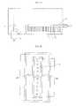
- the first injection unit 201may include a plurality of channels 2 and holes 3 respectively connected to each of the channels 2 . By providing the plurality of channels 2 through which the first material is transferred, the first material is uniformly injected over a large area of the substrate 1 .
- FIG. 5Bis a bottom view of the reaction module of FIG. 5A , according to one embodiment. As illustrated, a plurality of holes 3 may be arranged on the bottom surface of the first injection unit 201 with constant intervals to uniformly inject the first material onto the substrate. In FIG. 5B , the holes 4 are used for injecting the second material by the second injection unit 202 .
- FIG. 6Ais a cross-sectional view of a reaction module of a vapor deposition reactor, according to another embodiment.
- the reaction moduleincludes a first injection unit 201 and a second injection unit 202 .
- the first injection unit 201may have at least one first channel 5 and at least one second channel 6 . Different first materials may be injected through the first channel 5 and the second channel 6 . Further, the first channel 5 and the second channel 6 may have a first hole 7 and a second hole 8 , respectively.
- FIG. 6Bis a bottom view of the reaction module of FIG. 6B , according to one embodiment.
- the first hole 7 and the second hole 8is arranged to alternate on the bottom surface of the first injection unit 201 .
- two different first materialscan be uniformly injected onto the substrate.
- two sets of channels 5 , 6 and two sets of holes 7 , 8are provided to inject two kinds of first materials.
- more sets of channels and holesmay be provided depending on the types of the injected materials.
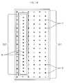
- FIG. 7Ais a bottom view of a reaction module of a vapor deposition reactor, according to one embodiment.
- a reaction modulemay include a first injection unit 201 and a second injection unit 202 .
- the second injection unit 202may have a first hole 4 and a second hole 9 through which different second materials are injected.
- the first and second holes 4 , 9may be connected to different channels, as described above in detail with reference to FIG. 6A .
- FIG. 7Bis a bottom view of a reaction module of a vapor deposition reactor, according to another embodiment.
- the second injection unit 202may have a first hole 4 and a second hole 9 through which different second materials are injected.
- the first and second holes 4 , 9 in FIG. 7Aare alternate in a single row.
- the first and second holes 4 , 9 in FIG. 7Bare arranged separately in two rows parallel to each other.
- a plurality of different second materialsmay be injected onto the substrate.
- a source precursormay be injected onto the substrate through the first hole 4
- a reactant precursormay be injected onto the substrate through the second hole 9 . Because both the source precursor and the reactant precursor are injected to the substrate when passing one reaction module, an atomic layer may be formed on the substrate using one reaction module.
- first hole 4 and the second hole 9 in FIGS. 7A and 7Bis merely illustrative and different arrangement may be used in other embodiments. Further, although two sets of holes 4 , 9 are provided to inject two types of second materials in the embodiment of FIGS. 7A and 7B , additional sets of holes may be provided depending on the type of the injected materials.
- FIG. 8is a cross-sectional view of a reaction module of a vapor deposition reactor, according to another embodiment.
- a reaction modulemay include a first injection unit 201 , a second injection unit 202 , and an exhaust unit 203 .
- the first injection unit 201may have a plasma generator 30 for radical-assisted atomic layer deposition (ALD).
- the first materialmay be applied to the substrate 1 in the form of plasma.
- the plasma generator 30may be well-known apparatuses.
- the plasma generator 30may apply voltage between coaxial electrodes facing each other to generate plasma of the reaction gas between the electrodes.
- the first injection unit 201may be used to excite (or decompose) an inorganic source precursor (which is difficult to attain in ALD) with plasma and form an atomic layer. That is, after inducing a primary reaction (or decomposition) of the source precursor by plasma energy, the source precursor may react with a reactant precursor. For example, by injecting an inorganic metal source such as TiCl 4 or SiH 4 to the substrate 1 as a source precursor by the first injection unit 201 and injecting NH 3 as a reactant precursor by the second injection unit 202 , TiN or SiN thin film may be formed on the substrate 1 .
- the resultant thin filmmay include residual Cl or H, as well as NH 4 Cl formed from the reaction of NH 3 and Cl.
- TiN thin filmmay be deposited at low temperature because Ti and Cl atoms are decomposed and Ti atoms are adsorbed at low temperature. Further, by injecting the source precursor mixed with TiCl 4 and H 2 by the first injection unit 201 , Ti atomic layer or a similar adsorption layer may be obtained by the plasma energy. Therefore, incubation or decreased deposition rate may be improved due to less adsorption.
- forming gas (N 2 +H 2 )is used as a reactant precursor in the second injection unit 202 , Ti thin film may be obtained on the substrate 1 . Si thin film may also be obtained in a similar way.
- a UV or ultrahigh frequency wave generatormay be provided in other embodiments to attain a similar effect.
- FIG. 9Ais a cross-sectional view of a reaction module of a vapor deposition reactor according to another exemplary embodiment.
- the reaction modulemay include, among others, a first injection unit 201 , a second injection unit 202 , a first electrode 41 and a second electrode 42 .
- the first and second electrodes 41 , 42generate plasma between the first injection unit 201 and the second injection unit 202 .
- the first electrode 41may be in contact with the inner wall of the first injection unit 201
- the second electrode 42may be in contact with the inner wall of the second injection unit 202 .
- the first and second electrodes 41 , 42are spaced apart from each other with a predetermined interval.
- the first electrode 41may include a hole for injecting a first material.
- the first injection unit 201may also be configured to inject a reaction gas for generating plasma in addition to the first material.
- an AC power or a pulsed powermay be applied by a power supply 40 .
- Plasmamay be generated from the reaction gas by the power applied between the first and second electrodes 41 , 42 . Radical activated by the plasma may be provided to a substrate 1 along with the first material, as described above in detail with reference to FIG. 8 .
- FIG. 9Bis a cross-sectional view of a reaction module of a vapor deposition reactor, according to another embodiment.
- First and second electrodes 41 , 42are arranged to apply an electric field in a direction parallel to the moving direction of the substrate 1 .
- the first and second electrodes 41 , 42may be provided in multiple pairs. Between each pair of the first and second electrodes 41 , 42 , voltage may be applied by a power supply 40 .
- a radical having a very short lifespansuch as hydrogen radical or nitrogen radical may be applied to the substrate 1 because plasma is generated directly above the substrate 1 . Further, damage of the substrate 1 attributable to the plasma may be minimized because the plasma is sprayed in a direction parallel to the surface of the substrate 1 .
- a single atomic layerhad to be formed by increasing the number of cycles when using a source precursor (e.g., TiCl 4 , SiH 4 , etc.) that does not exhibit the self-limiting phenomenon (i.e. source precursors do not exhibit saturation during chemical adsorption).
- a source precursore.g., TiCl 4 , SiH 4 , etc.
- the adsorption of the source precursoris sufficiently induced due to the surface activation by the plasma. As a result, no additional nucleation process is required and atomic layer can be formed without the incubation phenomenon.
- FIG. 10is a cross-sectional view of a reaction module of a vapor deposition reactor, according to another embodiment.
- the reaction module 20 of the vapor deposition reactormay include, among others, a plurality of first injection units 201 , 211 and a plurality of second injection units 202 , 212 placed within each of the first injection units 201 , 211 , respectively.
- the plurality of first injection units 201 , 211 and the second injection units 202 , 212may be placed within one exhaust unit 203 .
- a substrate 1When a substrate 1 is moved below the reaction module 20 from the left, an impurity or adsorbate on the substrate 1 may be removed by the exhaust unit 203 .
- a first materialis injected onto the substrate 1 by the first injection unit 201 .
- the first materialmay be a purge gas.
- a second materialis injected onto the substrate 1 by the second injection unit 202 .
- the second injection unit 202injects a reactant precursor onto the substrate 1 .
- the substrate 1sequentially passes the first injection unit 201 and then another first injection unit 211 . During this process, a first material may again be injected onto the substrate 1 .
- the second injection unit 212injects a source precursor onto the substrate 1 . Then, a thin film is formed on the substrate 1 by substitution and/or reaction of a chemical adsorption layer of the reactant precursor (injected by the second injection unit 202 ) with the source precursor injected by the second injection unit 212 . As the substrate 1 moves further to the right, the substrate 1 again passes the first injection unit 211 and the exhaust unit 203 , and then completely leaves from the reach of the reaction module 20 .
- the substrate 1passes one reaction module 20 , the following five stages are performed sequentially on the substrate 1 : (i) injection of the first material, (ii) injection of the second material (reactant precursor), (iii) injection of the first material, (iv) injection of the second material (source precursor), and (v) injection of the first material.
- a thin filmmay be formed on the substrate 1 .
- the stages of pumping by the exhaust unit 203may be added before and/or after the five stages.
- the first injection units 201 , 211 and the second injection units 211 , 212 illustrated in FIG. 10may be configured according to any of the embodiments described above with reference to FIGS. 2 to 9 . That is, at least one of the first injection units 201 , 211 may include a plasma generator, and at least one electrode for generation of plasma may be included between each pairs 201 - 211 , 202 - 212 of first injection unit and second injection unit. Further, at least one of the first injection units 201 , 211 and the second injection units 211 , 212 has a plurality of channels and holes. The configuration of a first injection unit 201 and another first injection unit 211 may be different. Likewise, the configuration of a second injection unit 211 and another second injection unit 212 may be different.
- a plurality of different materialsmay be injected onto a substrate by means of multiple injection units. Accordingly, a thin film may be formed by injecting a source precursor or a reactant precursor onto a substrate without exposing the substrate to the atmosphere in a chamber.
- the vapor deposition reactormay be used for ALD.
Landscapes
- Chemical & Material Sciences (AREA)
- General Chemical & Material Sciences (AREA)
- Chemical Kinetics & Catalysis (AREA)
- Engineering & Computer Science (AREA)
- Materials Engineering (AREA)
- Mechanical Engineering (AREA)
- Metallurgy (AREA)
- Organic Chemistry (AREA)
- Chemical Vapour Deposition (AREA)
Abstract
Description
- This application claims priority to under 35 U.S.C. §119(e) to co-pending U.S. Provisional Patent Application No. 61/088,677, filed on Aug. 13, 2008, which is incorporated by reference herein in its entirety.
- 1. Field of Art
- This invention relates to a vapor deposition reactor for forming a thin film on a substrate.
- 2. Description of the Related Art
- Semiconductor materials include silicon-based semiconductors such as Si and SiGe, metal oxide semiconductors such as ZnO, group III-V compound semiconductors such as GaAs, GaP, GaN, AlGaAs and InP; and group II-VI compound semiconductors such as CdSe, CdTe, ZnS and CdHgTe. Semiconductor devices are manufactured using these as substrate material, forming metal films or insulating films on the substrate material, and carrying out photolithography, etching, cleaning and thin film deposition.
- When fabricating a metal-oxide-semiconductor field-effect transistor (MOSFET) that is widely used in highly integrated circuits, an insulating film is formed on a semiconductor substrate. The insulating film is used as the gate insulating film for the transistor. Then, a metal film is formed on the substrate so that voltage or current required for driving the device can be applied. The reaction between the substrate and the metal film or the insulating film is important. In some cases, even a slight reaction may change of properties of semiconductor device. Therefore, a precise interface control is required to fabricate properly functioning semiconductor devices.
- Deposition techniques are gradually shifting from chemical vapor deposition (CVD) such as low-pressure CVD (LPCVD) performed in a furnace toward atomic layer deposition (ALD). ALD consists of the following four stages: (i) injecting a source precursor, (ii) removal of a physical adsorption layer, (iii) injection of a reactant precursor, and (iv) removal of a physical adsorption layer.
FIG. 1 is a flowchart illustrating ALD process according to a conventional technique. Referring toFIG. 1 , ALD process may include: loading a substrate (S11), passing the substrate by a source precursor injection module to inject a source precursor (S12), passing the substrate by a purge/pumping module to remove a physical adsorption layer from the source precursor (S13), passing the substrate by a reactant precursor supply module to inject a reactant precursor (S14), and passing the substrate by a purge/pumping module to remove a physical adsorption layer from the reactant precursor (S15). The above steps may be repeated until a layer with desired final thickness is obtained (S16). To perform these steps, an expensive valve that sequentially supplies the source precursor, purge gas, reactant precursor, and a purge gas to the substrate is needed.- Because the source precursor is deposited on the semiconductor substrate after removing natural oxide films from the semiconductor substrate using HF or other chemical substances, the source precursor comes in direct contact with the semiconductor substrate. While the source precursor remains in contact with the substrate, mutual diffusion or formation of unwanted interface may occur on the surface of the semiconductor substrate due to the reaction between the substrate and the source precursor. In case the semiconductor device has a sufficiently large design rule, such phenomena has minimal effect on the properties of the semiconductor device. However, if the design rule is about 32 nm or smaller, as in nano devices or quantum devices, the reactions at the interface or the unwanted formation of interface may become relevant.
- Embodiments provide a vapor deposition reactor capable of injecting a plurality of different materials to a substrate passing a reaction module using a plurality of injection units. The reaction module of the vapor deposition reactor is configured so that one injection unit is placed within another injection unit.
- In one embodiment, a vapor deposition reactor includes a reaction module. The reaction module includes a first injection unit for injecting a first material onto a substrate, and at least one second injection unit placed within the first injection unit for injecting a second material onto the substrate. The substrate passes the reaction module through a relative motion between the substrate and the reaction module.
FIG. 1 is a flowchart illustrating atomic layer deposition (ALD) process, according to a conventional process.FIG. 2 is a schematic perspective view of a vapor deposition reactor, according to one embodiment.FIG. 3A is a cross-sectional view of a vapor deposition reactor, according to one embodiment;FIG. 3B is a partially enlarged view of the vapor deposition reactor ofFIG. 3A , according to one embodiment.FIGS. 3C and 3D are cross-sectional views of a reaction module of a vapor deposition reactor according to embodiments.FIG. 3E is a cross-sectional view of a vapor deposition reactor according to another embodiment.FIG. 4A is a side cross-sectional view of a first injection unit of a vapor deposition reactor, according to one embodiment.FIGS. 4B to 4F are bottom views of a reaction module of a vapor deposition reactor, according to embodiments.FIG. 5A is a cross-sectional view of a reaction module of a deposition reactor, according to another embodiment.FIG. 5B is a bottom view of the reaction module ofFIG. 5A , according to one embodiment.FIG. 6A is a cross-sectional view of a reaction module of a vapor deposition reactor, according to one embodiment.FIG. 6B is a bottom view of the reaction module ofFIG. 6A , according to one embodiment.FIGS. 7A and 7B are bottom views of a reaction module of a vapor deposition reactor, according to embodiments.FIG. 8 is a cross-sectional view of a reaction module of a vapor deposition reactor, according to another embodiment.FIGS. 9A and 9B are cross-sectional views of a reaction module of a vapor deposition reactor, according to other embodiments.FIG. 10 is a cross-sectional view of a reaction module of a vapor deposition reactor, according to another embodiment.- Embodiments are described herein with reference to the accompanying drawings. Principles disclosed herein may, however, be embodied in many different forms and should not be construed as being limited to the embodiments set forth herein. In the description, details of well-known features and techniques may be omitted to avoid unnecessarily obscuring the features of the embodiments.
- The terminology used herein is for the purpose of describing particular exemplary embodiments only and is not intended to be limiting of this disclosure. As used herein, the singular forms “a”, “an” and “the” are intended to include the plural forms as well, unless the context clearly indicates otherwise. Furthermore, the use of the terms a, an, etc. does not denote a limitation of quantity, but rather denotes the presence of at least one of the referenced item. The use of the terms “first”, “second”, and the like does not imply any particular order, but they are included to identify individual elements. Moreover, the use of the terms first, second, etc. does not denote any order or importance, but rather the terms first, second, etc. are used to distinguish one element from another. It will be further understood that the terms “comprises” and/or “comprising”, or “includes” and/or “including” when used in this specification, specify the presence of stated features, regions, integers, steps, operations, elements, and/or components, but do not preclude the presence or addition of at least one other features, regions, integers, steps, operations, elements, components, and/or groups thereof.
- In the drawings, like reference numerals in the drawings denote like elements. The shape, size and regions, and the like, of the drawing may be exaggerated for clarity.
FIG. 2 is a schematic perspective view of a vapor deposition reactor according to an embodiment. The vapor deposition reactor may include, among others, at least onereaction module 20. The at least one reaction module is positioned in achamber 10. Inside thechamber 10, at least one substrate1 is loaded onto asupport 100. The interior of thechamber 10 may be in a vacuum state. If needed to lower the base vacuum level of thechamber 10 to 10−3Torr or lower to form a thin film (e.g., e.g. metal film) susceptible to residual oxygen, a vacuum pump such as a turbo-molecular pump (TMP) may be equipped in thechamber 10. Alternatively, thechamber 10 may be filled with a material.- The temperature of the substrate1 and the atmosphere in the
chamber 10 may affect the reaction. Hence, a heating apparatus (not shown) may be provided to control the temperature inside thechamber 10. When the heating apparatus is disposed below thechamber 10 to heat the substrate1 indirectly, the space used for deposition is separated from the heating apparatus by thechamber 10, thesupport 100, etc. The heating apparatus may be purged by injecting an inert gas such as Ar such that materials used for deposition does not flow into the heating apparatus. The pressure of the injected purge gas may be controlled to be not lower than that of the space used for deposition so that the purge gas does not deteriorate deposition properties. - Although the
chamber 10 illustrated inFIG. 2 has a cylindrical shape, this is merely illustrative. Thechamber 10 may have any other arbitrary shape as long as thechamber 10 can accommodate the substrate1 and thereaction module 20. The shape of the substrate1 is also not limited to the disc shape illustrated inFIG. 2 , but may be any arbitrary shape. - The at least one
reaction module 20 may be fixed inside thechamber 10 but thesupport 100 holding the substrate1 may rotate. The rotating speed of thesupport 100 may be constant. Alternatively, the rotating speed of thesupport 100 may be controlled using a computing device to vary the rotating speed depending on positions. As thesupport 100 rotates, the substrate1 may pass below thereaction module 20. In another embodiment, the substrate1 may be fixed and thereaction module 20 may be rotated to generate a relative motion between the substrate1 and thereaction module 20. - In the vapor deposition reactor of the above embodiment, the relative motion between the substrate1 and the
reaction module 20 is rotation. In other embodiments, the relative motion between the substrate1 and thereaction module 20 may be a linear or reciprocal motion. - While the substrate1 passes below the
reaction module 20, the substrate1 may be separated from the bottom surface of thereaction module 20 by a predetermined distance to maintain a non-contact state. The substrate1 passing below thereaction module 20 may be exposed to the material injected from thereaction module 20. As a result, an adsorption layer is formed on the substrate1. - The material injected from each
reaction module 20 may be the same or different. For example, by injecting a reactant precursor using onereaction module 20 and injecting a source precursor using anotherreaction module 20, an atomic layer may be formed on the substrate1 as the substrate1 passing the tworeaction modules 20, as described below in detail with reference toFIGS. 3A and 3B . - In one embodiment, depending on the type of the thin film desired, the
reaction module 20 may include a plasma generator, ultrahigh frequency wave generator or UV generator. These energy sources may be used in combination with the same process or these energy sources may be used sequentially in different processes to form a thin film, as described below in detail. FIG. 3A is a cross-sectional view of a vapor deposition reactor according to one embodiment.FIG. 3B is a partially enlarged view of a portion where a substrate1 and areaction module 20 are adjacent to each other in the vapor deposition reactor ofFIG. 3A . The substrate1 fixed onto asusceptor 101 of asupport 100 moves from the left to the right. That is, the substrate1 passes the lower portion of thereaction module 20 from the left to the right. The substrate1 and thereaction module 20 may be spaced apart from each other and maintain a non-contact state. For example, the distance between the substrate1 and the reaction module may be about 1 mm to about several millimeters. Before the substrate1 passes the lower portion thereaction module 20, impurities or adsorbates may be formed on the surface of the substrate1 due to the presence of atmosphere in achamber 10.- In one embodiment, the
chamber 10 includes achannel 115 at a region adjacent to the substrate1. In this case, the remaining region of thechamber 10 excluding thechannel 115 may be filled with afiller 110. Thefiller 110 may be the same as the material constituting the outer wall of thechamber 10. Such a configuration is economically advantageous because the amount of the material needed to fill thechamber 10 may be reduced. - The
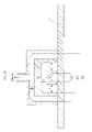
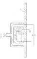
reaction module 20 may include afirst injection unit 201, and asecond injection unit 202 positioned within thefirst injection unit 201. Further, the first andsecond injection units exhaust unit 203. The size of thereaction module 20 and the size of each of thefirst injection unit 201,second injection unit 202 andexhaust unit 203 may be set adequately depending on the materials or the types of thin films to be formed. Theexhaust unit 203 and thefirst injection unit 201 may be spaced apart from each other in a direction perpendicular to the direction of movement of the substrate1 by a distance H. Further, thefirst injection unit 201 and thesecond injection unit 202 may be spaced apart from each other in a direction perpendicular to the direction of movement of the substrate1 by a distance Z. In addition, the first andsecond injection units - When all or part of the substrate1 from the left side of the figure is positioned below the
exhaust unit 203 of thereaction module 20, the impurity or adsorbate is discharged out of thechamber 10 by theexhaust unit 203. When the substrate1 moves further to the right and the corresponding region is positioned below thefirst injection unit 201, thefirst injection unit 201 injects a first material to the substrate1. For example, the first material is a purge gas. By injecting the purge gas onto the substrate1, the molecules physically adsorbed in the surface of the substrate1 may be removed. As a result, only a chemical adsorption layer formed by preceding processes remains on the substrate1. Alternatively, if there was no preceding process, the substrate1 may be void of an adsorption layer. The purge gas may be an inert gas. For example, the purge gas may include N2gas, Ar gas, He gas, or other suitable material. Further, the purge gas may include a combination of two or more of above materials. The first material may include a source precursor or a reactant precursor for forming an atomic layer. - When the substrate1 moves further to the right and all or part of the substrate1 is positioned below the
second injection unit 202, theinjection unit 202 injects a second material to the substrate1. The second material may be a material for forming a thin film on the substrate1. For example, the second material includes a source precursor or a reactant precursor for forming an atomic layer. - The reactant precursor may be a material for obtaining metal, oxide, nitride, carbide or semiconductor material from a chemical source. For example, the first material may include H2O, H2O2, O2, N2O, O3, O* radical, NH3, NH2—NH2, N2, N* radical, organic carbon compounds such as CH4, C2H6, etc., H2, H* radical, or other suitable material. The first material may include a combination of two or more of above materials.
- Further, the source precursor may be a material capable of forming a thin film on the substrate1 by reaction and/or substitution with the reactant precursor. A variety of materials may be used as the source precursor depending on the thin film to be formed. For example, in case the thin film is made of a semiconductor, the source precursor may be group IV compounds, group III-V compounds, group II-VI compounds, or the like. In case the thin film is made of a metal, the source precursor may be Ni-based compounds, Co-based compounds, Al-based compounds, Ti-based compounds, Hf-based compounds, Zr-based compounds, Ta-based compounds, Mo-based compounds, W-based compounds, or compounds including above materials and Si. In case the thin film is made of a dielectric or a conductive dielectric, the source precursor may be Ni-based compounds, Zn-based compounds, Cu-based compounds, Co-based compounds, Al-based compounds, Si-based compounds, Hf-based compounds, Ti-based compounds, Zr-based compounds, Ta-based compounds, or the like. The source precursor may include a combination of two or more of the above materials.
- For example, Si-based compounds used as the second material may include SiH4, SiH2Cl2, or the like. Ti-based compounds used as the second material may include TiCl4, or the like. Al-based compounds used as the second material may include trimethylaluminum (TMA), or the like. Hf-based compounds used as the second material may include tetrakis-ethylmethylaminohafnium (TEMAHf), or the like. Zr-based compounds used as the second material may include tetrakis-ethylmethylaminozirconium (TEMAZr), or the like. The kind of the second materials is not limited to these materials, and other materials not listed herein may also be used depending on the kind of the final thin film.
- The reactant precursor may be in the form of plasma of the above material, or may be supplied along with light such as UV light. Even when the reactant precursor is decomposed by applying plasma, radical, or photon, it is not likely that the byproduct remains in the final thin film or the property of the thin film is deteriorated or degraded. If the reactant precursor is activated by such energy, a sufficient adsorption of molecules may be attained even when Si-based compounds or TiCl4, which do not readily form a thin film, are used as the source precursor. As a result, the rate of thin film deposition may be increased and the surface treatment or interface treatment of the substrate1 may be facilitated.
- The first and
second injection units support 100 rotates, the first andsecond injection units - When the substrate1 moves further to the right and passes the
second injection unit 202, the substrate1 is positioned again below thefirst injection unit 201. Thefirst injection unit 201 may inject the first material such as a purge gas onto the substrate1. A physical adsorption layer and a chemical adsorption layer of the second material may be formed on the substrate1 that has passed thesecond injection unit 202. The physical adsorption layer may be separated from the substrate1 by the purge gas injected from thefirst injection unit 201. - When the substrate1 moves further to the right, the substrate1 becomes positioned below the
exhaust unit 203. At this location, the purge gas and the physical adsorption layer of the second material are removed by pumping the purge gas and the physical absorption layer out of thechamber 10. As a result, only the chemical adsorption layer of the second material remains on the surface of the substrate1 after passing thereaction module 20. - As the substrate1 passes one
reaction module 20, the following three stages are preformed sequentially on the substrate1: (i) injection of the first material, (ii) injection of the second material (reactant precursor or source precursor), and (iii) injection of the first material. Stages of pumping by theexhaust unit 203 may be added before and/or after the three stages. By changing the position of the second injection unit202 (or separating thesecond injection unit 202 from the first injection unit201), the time interval during which the substrate1 passes the distance Y between thefirst injection unit 201 and thesecond injection unit 202 is changed, and thus, the time interval for injecting the first material is changed accordingly. Therefore, using precursors having different adsorption properties is advantageous in optimizing the purge amount and purge time. As a result, only the chemical adsorption layer of the reactant precursor or the source precursor remains on the surface of the substrate1 after passing thereaction module 20. - In one embodiment wherein the distance Y between the
first injection unit 201 and thesecond injection unit 202 is decreased, a portion of the physical adsorption layer of the reactant precursor or the source precursor remains on the substrate1 because the purge time of the reactant precursor or the source precursor may be insufficient. Compared to depositing a thin film by a pure atomic layer, the remaining physical adsorption layer may increase the rate of deposition of the thin film. - The substrate1 with the chemical adsorption layer of the reactant precursor or the source precursor may pass another
reaction module 20 to form a thin film on the substrate1. For example, a substrate1 with a chemical adsorption layer of the reactant precursor formed by passing onereaction module 20 may pass anotherreaction module 20 injecting the source precursor. As a result, an atomic layer may be formed on the substrate1 by substitution and/or reaction of the reactant precursor with the source precursor. On the contrary, a chemical adsorption layer of the source precursor may be first formed on the substrate1 by onereaction module 20, and then the reactant precursor may be injected by anotherreaction module 20 to form an atomic layer. FIGS. 3C and 3D are cross-sectional views of a reaction module of a vapor deposition reactor, according to other embodiments. The distance X (seeFIG. 3B ) between thefirst injection unit 201 and thesecond injection unit 202 in the direction opposite to the movement direction of the substrate1 may be 0. That is, thesecond injection unit 201 is in contact with the inner wall of thefirst injection unit 201 as illustrated inFIG. 3C . Alternatively, thesecond injection unit 202 is in contact with an inner wall of thefirst injection unit 201 at the opposite side, as illustrated inFIG. 3D . As illustrated inFIGS. 3C and 3D , parameters for performing deposition may be varied by controlling the distances X, Y, Z between the first andsecond injection units FIG. 3E is a cross-sectional view of a vapor deposition reactor, according to another embodiment. In this embodiment, the purge gas is sprayed from a side wall of thefirst injection unit 201. As the sprayed purge gas passes the substrate1, a portion of the precursors adsorbed on the substrate1 is desorbed from the substrate1. The desorbed precursors are then discharged by theexhaust unit 203. Thesecond injection unit 202 may be in contact with an upper portion of the inner surface of thefirst injection unit 201. The purge gas is sprayed from a side wall of thefirst injection unit 201. Thus, the purge gas is sprayed in a direction opposite to the moving direction of the substrate1 and is discharged by theexhaust unit 203. Alternatively, in another embodiment, the purge gas is sprayed from a side wall of thefirst injection unit 201 opposite to the side wall as illustrated inFIG. 3E .- A detailed description on the operation of the vapor deposition reactor illustrated in
FIGS. 3C to 3E is omitted herein for the purpose of brevity. FIG. 4A is a side cross-sectional view of afirst injection unit 201 of a vapor deposition reactor, according to one embodiment. As illustrated inFIG. 4A , thefirst injection unit 201 includes a pipe-shapedchannel 2 through which the first material is injected and transferred. The first material transferred through thechannel 2 is injected onto the substrate below through at least onehole 3 formed in thechannel 2. Eachhole 3 may have the same or different size. Although an example configuration of thefirst injection unit 201 is shown inFIG. 4A , the configuration of thesecond injection unit 202 may also be the same.FIG. 4B is a bottom view of a reaction module of a vapor deposition reactor, according to one embodiment. As illustrated, thesecond injection unit 202 may be placed in thefirst injection unit 201 spaced apart from thefirst injection unit 201. The second material may be injected through at least onehole 3 of thesecond injection unit 202. InFIG. 4B , the hole of thefirst injection unit 201 is not illustrated it is occluded by thesecond injection unit 202.FIG. 4C is a bottom view of a reaction module of a vapor deposition reactor, according to another embodiment. As illustrated, thesecond injection unit 202 is positioned in thefirst injection unit 201 in contact with at least one inner wall of thefirst injection unit 201. However, thesecond injection unit 202 should be spaced apart from at least one of the inner walls of thefirst injection unit 201 because the first material is injected onto the substrate by thefirst injection unit 201.FIG. 4D is a bottom view of a reaction module of a vapor deposition reactor, according to another embodiment. As illustrated inFIG. 4D , thefirst injection unit 201 and thesecond injection unit 202 have circular cross-sections. For example, thefirst injection unit 201 and thesecond injection unit 202 may have the shape of a circular cylinder. Thesecond injection unit 202 may be placed in thefirst injection unit 201 spaced apart from thefirst injection unit 201. The second material may be injected through at least onehole 3 of thesecond injection unit 202. InFIG. 4D , the hole of thefirst injection unit 201 is not illustrated because the hole is occluded by thesecond injection unit 202.FIGS. 4E and 4F are bottom views of a reaction module of a vapor deposition reactor, according to other embodiments. Referring toFIG. 4E , thesecond injection unit 202 may be positioned in thefirst injection unit 201 while in contact with an inner wall of thefirst injection unit 201. Referring toFIG. 4F , thesecond injection unit 202 may be in contact with the inner wall of thefirst injection unit 201 from a direction different from that ofFIG. 4E .- The cross-sections of the reaction module shown in
FIGS. 4B to 4F are merely illustrative. The reaction module may have a cross-section of different shapes. FIG. 5A is a cross-sectional view of a reaction module of a deposition reactor, according to another embodiment. The reaction module may include afirst injection unit 201 and asecond injection unit 202. Thefirst injection unit 201 may include a plurality ofchannels 2 andholes 3 respectively connected to each of thechannels 2. By providing the plurality ofchannels 2 through which the first material is transferred, the first material is uniformly injected over a large area of the substrate1.FIG. 5B is a bottom view of the reaction module ofFIG. 5A , according to one embodiment. As illustrated, a plurality ofholes 3 may be arranged on the bottom surface of thefirst injection unit 201 with constant intervals to uniformly inject the first material onto the substrate. InFIG. 5B , theholes 4 are used for injecting the second material by thesecond injection unit 202.FIG. 6A is a cross-sectional view of a reaction module of a vapor deposition reactor, according to another embodiment. The reaction module includes afirst injection unit 201 and asecond injection unit 202. Thefirst injection unit 201 may have at least one first channel5 and at least onesecond channel 6. Different first materials may be injected through the first channel5 and thesecond channel 6. Further, the first channel5 and thesecond channel 6 may have afirst hole 7 and asecond hole 8, respectively.FIG. 6B is a bottom view of the reaction module ofFIG. 6B , according to one embodiment. As illustrated, thefirst hole 7 and thesecond hole 8 is arranged to alternate on the bottom surface of thefirst injection unit 201. With such a configuration, two different first materials can be uniformly injected onto the substrate. In the embodiment ofFIGS. 6A and 6B , two sets ofchannels 5,6 and two sets ofholes FIG. 7A is a bottom view of a reaction module of a vapor deposition reactor, according to one embodiment. A reaction module may include afirst injection unit 201 and asecond injection unit 202. Thesecond injection unit 202 may have afirst hole 4 and asecond hole 9 through which different second materials are injected. The first andsecond holes FIG. 6A .FIG. 7B is a bottom view of a reaction module of a vapor deposition reactor, according to another embodiment. Thesecond injection unit 202 may have afirst hole 4 and asecond hole 9 through which different second materials are injected. The first andsecond holes FIG. 7A are alternate in a single row. The first andsecond holes FIG. 7B are arranged separately in two rows parallel to each other.- With the configuration illustrated in
FIG. 7A or7B, a plurality of different second materials may be injected onto the substrate. For example, a source precursor may be injected onto the substrate through thefirst hole 4, and a reactant precursor may be injected onto the substrate through thesecond hole 9. Because both the source precursor and the reactant precursor are injected to the substrate when passing one reaction module, an atomic layer may be formed on the substrate using one reaction module. - The arrangement of the
first hole 4 and thesecond hole 9 inFIGS. 7A and 7B is merely illustrative and different arrangement may be used in other embodiments. Further, although two sets ofholes FIGS. 7A and 7B , additional sets of holes may be provided depending on the type of the injected materials. FIG. 8 is a cross-sectional view of a reaction module of a vapor deposition reactor, according to another embodiment. A reaction module may include afirst injection unit 201, asecond injection unit 202, and anexhaust unit 203. Thefirst injection unit 201 may have aplasma generator 30 for radical-assisted atomic layer deposition (ALD). The first material may be applied to the substrate1 in the form of plasma. Theplasma generator 30 may be well-known apparatuses. For example, theplasma generator 30 may apply voltage between coaxial electrodes facing each other to generate plasma of the reaction gas between the electrodes.- The
first injection unit 201 may be used to excite (or decompose) an inorganic source precursor (which is difficult to attain in ALD) with plasma and form an atomic layer. That is, after inducing a primary reaction (or decomposition) of the source precursor by plasma energy, the source precursor may react with a reactant precursor. For example, by injecting an inorganic metal source such as TiCl4or SiH4to the substrate1 as a source precursor by thefirst injection unit 201 and injecting NH3as a reactant precursor by thesecond injection unit 202, TiN or SiN thin film may be formed on the substrate1. However, the resultant thin film may include residual Cl or H, as well as NH4Cl formed from the reaction of NH3and Cl. - However, when the
first injection unit 201 injects TiCl4in the form of plasma as described above, TiN thin film may be deposited at low temperature because Ti and Cl atoms are decomposed and Ti atoms are adsorbed at low temperature. Further, by injecting the source precursor mixed with TiCl4and H2by thefirst injection unit 201, Ti atomic layer or a similar adsorption layer may be obtained by the plasma energy. Therefore, incubation or decreased deposition rate may be improved due to less adsorption. When forming gas (N2+H2) is used as a reactant precursor in thesecond injection unit 202, Ti thin film may be obtained on the substrate1. Si thin film may also be obtained in a similar way. - Although the
plasma generator 30 is provided in thefirst injection unit 201 of the above embodiments, a UV or ultrahigh frequency wave generator may be provided in other embodiments to attain a similar effect. FIG. 9A is a cross-sectional view of a reaction module of a vapor deposition reactor according to another exemplary embodiment. Referring toFIG. 9A , the reaction module may include, among others, afirst injection unit 201, asecond injection unit 202, afirst electrode 41 and asecond electrode 42. The first andsecond electrodes first injection unit 201 and thesecond injection unit 202.- The
first electrode 41 may be in contact with the inner wall of thefirst injection unit 201, and thesecond electrode 42 may be in contact with the inner wall of thesecond injection unit 202. The first andsecond electrodes first electrode 41 is adjacent to a channel of thefirst injection unit 201, thefirst electrode 41 may include a hole for injecting a first material. Thefirst injection unit 201 may also be configured to inject a reaction gas for generating plasma in addition to the first material. - Between the first and
second electrodes power supply 40. Plasma may be generated from the reaction gas by the power applied between the first andsecond electrodes FIG. 8 . FIG. 9B is a cross-sectional view of a reaction module of a vapor deposition reactor, according to another embodiment. First andsecond electrodes second electrodes second electrodes power supply 40.- Using such a reaction module, a radical having a very short lifespan such as hydrogen radical or nitrogen radical may be applied to the substrate1 because plasma is generated directly above the substrate1. Further, damage of the substrate1 attributable to the plasma may be minimized because the plasma is sprayed in a direction parallel to the surface of the substrate1.
- In conventional reactors, a single atomic layer had to be formed by increasing the number of cycles when using a source precursor (e.g., TiCl4, SiH4, etc.) that does not exhibit the self-limiting phenomenon (i.e. source precursors do not exhibit saturation during chemical adsorption). However, when the vapor deposition reactor according to embodiments is used, the adsorption of the source precursor is sufficiently induced due to the surface activation by the plasma. As a result, no additional nucleation process is required and atomic layer can be formed without the incubation phenomenon.
FIG. 10 is a cross-sectional view of a reaction module of a vapor deposition reactor, according to another embodiment. Thereaction module 20 of the vapor deposition reactor may include, among others, a plurality offirst injection units 201,211 and a plurality ofsecond injection units 202,212 placed within each of thefirst injection units 201,211, respectively. The plurality offirst injection units 201,211 and thesecond injection units 202,212 may be placed within oneexhaust unit 203.- An illustrative process of forming a thin film using the vapor deposition reactor according to embodiments is described herein. When a substrate1 is moved below the
reaction module 20 from the left, an impurity or adsorbate on the substrate1 may be removed by theexhaust unit 203. When the substrate1 moves further to the right and is placed below thefirst injection unit 201, a first material is injected onto the substrate1 by thefirst injection unit 201. The first material may be a purge gas. - When the substrate1 moves further to the right and is positioned below the
second injection unit 202, a second material is injected onto the substrate1 by thesecond injection unit 202. For example, thesecond injection unit 202 injects a reactant precursor onto the substrate1. After passing thesecond injection unit 202, the substrate1 sequentially passes thefirst injection unit 201 and then another first injection unit211. During this process, a first material may again be injected onto the substrate1. - When the substrate moves further to the right and is positioned below the second injection unit212, another second material is injected to the substrate1 by the second injection unit212. For example, the second injection unit212 injects a source precursor onto the substrate1. Then, a thin film is formed on the substrate1 by substitution and/or reaction of a chemical adsorption layer of the reactant precursor (injected by the second injection unit202) with the source precursor injected by the second injection unit212. As the substrate1 moves further to the right, the substrate1 again passes the first injection unit211 and the
exhaust unit 203, and then completely leaves from the reach of thereaction module 20. - As the substrate1 passes one
reaction module 20, the following five stages are performed sequentially on the substrate1: (i) injection of the first material, (ii) injection of the second material (reactant precursor), (iii) injection of the first material, (iv) injection of the second material (source precursor), and (v) injection of the first material. As a result, a thin film may be formed on the substrate1. Further, the stages of pumping by theexhaust unit 203 may be added before and/or after the five stages. - The
first injection units 201,211 and the second injection units211,212 illustrated inFIG. 10 may be configured according to any of the embodiments described above with reference toFIGS. 2 to 9 . That is, at least one of thefirst injection units 201,211 may include a plasma generator, and at least one electrode for generation of plasma may be included between each pairs201-211,202-212 of first injection unit and second injection unit. Further, at least one of thefirst injection units 201,211 and the second injection units211,212 has a plurality of channels and holes. The configuration of afirst injection unit 201 and another first injection unit211 may be different. Likewise, the configuration of a second injection unit211 and another second injection unit212 may be different. - Using the vapor deposition reactor according to embodiments, a plurality of different materials may be injected onto a substrate by means of multiple injection units. Accordingly, a thin film may be formed by injecting a source precursor or a reactant precursor onto a substrate without exposing the substrate to the atmosphere in a chamber. The vapor deposition reactor may be used for ALD.
- Although the present invention has been described above with respect to several embodiments, various modifications can be made within the scope of the present invention. Accordingly, the disclosure of the present invention is intended to be illustrative, but not limiting, of the scope of the invention, which is set forth in the following claims.
Claims (18)
Priority Applications (1)
| Application Number | Priority Date | Filing Date | Title |
|---|---|---|---|
| US12/539,490US20100037820A1 (en) | 2008-08-13 | 2009-08-11 | Vapor Deposition Reactor |
Applications Claiming Priority (2)
| Application Number | Priority Date | Filing Date | Title |
|---|---|---|---|
| US8867708P | 2008-08-13 | 2008-08-13 | |
| US12/539,490US20100037820A1 (en) | 2008-08-13 | 2009-08-11 | Vapor Deposition Reactor |
Publications (1)
| Publication Number | Publication Date |
|---|---|
| US20100037820A1true US20100037820A1 (en) | 2010-02-18 |
Family
ID=41680371
Family Applications (1)
| Application Number | Title | Priority Date | Filing Date |
|---|---|---|---|
| US12/539,490AbandonedUS20100037820A1 (en) | 2008-08-13 | 2009-08-11 | Vapor Deposition Reactor |
Country Status (1)
| Country | Link |
|---|---|
| US (1) | US20100037820A1 (en) |
Cited By (48)
| Publication number | Priority date | Publication date | Assignee | Title |
|---|---|---|---|---|
| US20090165715A1 (en)* | 2007-12-27 | 2009-07-02 | Oh Jae-Eung | Vapor deposition reactor |
| US20100041213A1 (en)* | 2008-08-13 | 2010-02-18 | Synos Technology, Inc. | Vapor Deposition Reactor For Forming Thin Film |
| US20100037824A1 (en)* | 2008-08-13 | 2010-02-18 | Synos Technology, Inc. | Plasma Reactor Having Injector |
| US20100064971A1 (en)* | 2008-09-17 | 2010-03-18 | Synos Technology, Inc. | Electrode for Generating Plasma and Plasma Generator |
| US20100068413A1 (en)* | 2008-09-17 | 2010-03-18 | Synos Technology, Inc. | Vapor deposition reactor using plasma and method for forming thin film using the same |
| US20100181566A1 (en)* | 2009-01-21 | 2010-07-22 | Synos Technology, Inc. | Electrode Structure, Device Comprising the Same and Method for Forming Electrode Structure |
| US20100215871A1 (en)* | 2009-02-23 | 2010-08-26 | Synos Technology, Inc. | Method for forming thin film using radicals generated by plasma |
| US20100310771A1 (en)* | 2009-06-08 | 2010-12-09 | Synos Technology, Inc. | Vapor deposition reactor and method for forming thin film |
| US20110076421A1 (en)* | 2009-09-30 | 2011-03-31 | Synos Technology, Inc. | Vapor deposition reactor for forming thin film on curved surface |
| US20110232572A1 (en)* | 2010-03-29 | 2011-09-29 | Hon Hai Precision Industry Co., Ltd. | Plasma film-coating apparatus |
| WO2012028784A1 (en)* | 2010-08-30 | 2012-03-08 | Beneq Oy | Apparatus and method |
| WO2012061278A1 (en)* | 2010-11-05 | 2012-05-10 | Synos Technology, Inc. | Radical reactor with multiple plasma chambers |
| US20120125258A1 (en)* | 2010-11-24 | 2012-05-24 | Synos Technology, Inc. | Extended Reactor Assembly with Multiple Sections for Performing Atomic Layer Deposition on Large Substrate |
| US20120222615A1 (en)* | 2010-09-03 | 2012-09-06 | Tokyo Electron Limited | Film deposition apparatus |
| US20120247390A1 (en)* | 2009-09-17 | 2012-10-04 | Tokyo Electron Limited | Film formation apparatus |
| WO2012112584A3 (en)* | 2011-02-16 | 2012-10-11 | Synos Technology, Inc | Atomic layer deposition using radicals of gas mixture |
| WO2013121102A2 (en) | 2012-02-17 | 2013-08-22 | Beneq Oy | Nozzle and nozzle head |
| US20140023796A1 (en)* | 2011-03-31 | 2014-01-23 | Toray Industries, Inc. | Plasma cvd apparatus, plasma cvd method, reactive sputtering apparatus, and reactive sputtering method |
| US20140044889A1 (en)* | 2012-08-10 | 2014-02-13 | Globalfoundries Inc. | Methods of making stressed material layers and a system for forming such layers |
| US20140120257A1 (en)* | 2012-10-25 | 2014-05-01 | Applied Materials, Inc. | Apparatus for selective gas injection and extraction |
| US8771791B2 (en) | 2010-10-18 | 2014-07-08 | Veeco Ald Inc. | Deposition of layer using depositing apparatus with reciprocating susceptor |
| US20140205769A1 (en)* | 2013-01-22 | 2014-07-24 | Veeco Ald Inc. | Cascaded plasma reactor |
| KR101430658B1 (en)* | 2012-05-29 | 2014-08-18 | 주식회사 에스에프에이 | Atomic layer deposition system |
| US8840958B2 (en) | 2011-02-14 | 2014-09-23 | Veeco Ald Inc. | Combined injection module for sequentially injecting source precursor and reactant precursor |
| US20150031167A1 (en)* | 2013-07-25 | 2015-01-29 | Samsung Display Co., Ltd. | Deposition apparatus, method of forming thin film using the deposition apparatus, and method of manufacturing organic light emitting display apparatus using the deposition apparatus |
| CN104350581A (en)* | 2012-05-30 | 2015-02-11 | 周星工程股份有限公司 | Substrate treating apparatus and method |
| US20150050421A1 (en)* | 2013-08-14 | 2015-02-19 | Samsung Display Co., Ltd. | Method of depositing an atomic layer and atomic layer deposition apparatus |
| US20150079807A1 (en)* | 2013-09-13 | 2015-03-19 | Tokyo Electron Limited | Method of manufacturing a silicon oxide film |
| US20150087160A1 (en)* | 2013-09-20 | 2015-03-26 | Hitachi Kokusai Electric Inc. | Substrate processing apparatus, method of manufacturing semiconductor device, and recording medium |
| CN104871293A (en)* | 2013-02-04 | 2015-08-26 | Tes股份有限公司 | Thin-film vapour deposition device |
| JP2015526595A (en)* | 2012-06-29 | 2015-09-10 | ジュスン エンジニアリング カンパニー リミテッド | Substrate processing apparatus and substrate processing method |
| US9163310B2 (en) | 2011-02-18 | 2015-10-20 | Veeco Ald Inc. | Enhanced deposition of layer on substrate using radicals |
| US20160138157A1 (en)* | 2014-11-14 | 2016-05-19 | Samsung Display Co., Ltd. | Thin film deposition apparatus |
| US9376455B2 (en) | 2013-11-27 | 2016-06-28 | Veeco Ald Inc. | Molecular layer deposition using reduction process |
| WO2016102771A1 (en)* | 2014-12-22 | 2016-06-30 | Beneq Oy | Nozzle head and apparatus for coating substrate surface |
| US20170058402A1 (en)* | 2015-08-28 | 2017-03-02 | Samsung Electronics Co., Ltd. | Shower head of combinatorial spatial atomic layer deposition apparatus |
| US20180277400A1 (en)* | 2017-03-23 | 2018-09-27 | Toshiba Memory Corporation | Semiconductor manufacturing apparatus |
| US20190184187A1 (en)* | 2016-08-02 | 2019-06-20 | Feagle Co., Ltd | Plasma treatment apparatus |
| US10358721B2 (en)* | 2015-10-22 | 2019-07-23 | Asm Ip Holding B.V. | Semiconductor manufacturing system including deposition apparatus |
| KR20190101303A (en)* | 2018-02-22 | 2019-08-30 | 유니버셜 디스플레이 코포레이션 | Modular confined organic print head and system |
| US20190292662A1 (en)* | 2018-03-26 | 2019-09-26 | Tokyo Electron Limited | Film-forming method and film-forming apparatus |
| EP3478871A4 (en)* | 2016-06-30 | 2020-04-01 | Beneq OY | METHOD AND DEVICES FOR COATING A SUBSTRATE |
| US11239057B2 (en)* | 2017-07-28 | 2022-02-01 | Sumitomo Electric Industries, Ltd. | Showerhead and method for manufacturing the same |
| US11339472B2 (en)* | 2019-05-10 | 2022-05-24 | Tokyo Electron Limited | Substrate processing apparatus |
| US20230032292A1 (en)* | 2021-07-28 | 2023-02-02 | Changxin Memory Technologies, Inc. | Method for forming thin film by deposition process |
| US11837445B2 (en)* | 2018-11-14 | 2023-12-05 | Jusung Engineering Co., Ltd. | Substrate processing device and substrate processing method |
| US20240368760A1 (en)* | 2023-05-05 | 2024-11-07 | Lotus Applied Technology, Llc | Methods and systems for inhibiting precursor interactions during radical-enhanced atomic layer deposition |
| US12325915B2 (en) | 2019-11-28 | 2025-06-10 | Picosun Oy | Substrate processing apparatus and method |
Citations (108)
| Publication number | Priority date | Publication date | Assignee | Title |
|---|---|---|---|---|
| US788688A (en)* | 1903-08-01 | 1905-05-02 | William E Wild | Machine for classifying and sizing ores. |
| US3896244A (en)* | 1971-11-17 | 1975-07-22 | Chromalloy American Corp | Method of producing plasma sprayed titanium carbide tool steel coatings |
| JPS6281018A (en)* | 1985-10-04 | 1987-04-14 | Hitachi Ltd | Normal pressure CVD equipment |
| JPH0196924A (en)* | 1987-10-09 | 1989-04-14 | Matsushita Electric Ind Co Ltd | Film forming method using thermal CVD method |
| JPH01223724A (en)* | 1988-03-02 | 1989-09-06 | Mitsubishi Electric Corp | Chemical vapor growth device |
| US4891247A (en)* | 1986-09-15 | 1990-01-02 | Watkins-Johnson Company | Process for borosilicate glass films for multilevel metallization structures in semiconductor devices |
| JPH02187018A (en)* | 1989-01-13 | 1990-07-23 | Mitsubishi Electric Corp | chemical vapor deposition equipment |
| JPH0492414A (en)* | 1990-08-08 | 1992-03-25 | Mitsubishi Electric Corp | Thin film formation device |
| US5120568A (en)* | 1987-06-16 | 1992-06-09 | Shell Oil Company | Method for plasma surface treating and preparation of membrane layers |
| US5122391A (en)* | 1991-03-13 | 1992-06-16 | Watkins-Johnson Company | Method for producing highly conductive and transparent films of tin and fluorine doped indium oxide by APCVD |
| US5136975A (en)* | 1990-06-21 | 1992-08-11 | Watkins-Johnson Company | Injector and method for delivering gaseous chemicals to a surface |
| US5275668A (en)* | 1990-08-20 | 1994-01-04 | Dell Joseph G | Hydro impact medical and dental instruments washer |
| US5286295A (en)* | 1991-02-13 | 1994-02-15 | Saint-Gobain Vitrage International | Nozzle with nonsymmetrical feed for the formation of a coating layer on a ribbon of glass, by pyrolysis of a gas mixture |
| US5300189A (en)* | 1986-05-21 | 1994-04-05 | Hitachi, Ltd. | Plasma surface treatment method and apparatus |
| US5482557A (en)* | 1986-01-14 | 1996-01-09 | Canon Kabushiki Kaisha | Device for forming deposited film |
| US5549780A (en)* | 1990-10-23 | 1996-08-27 | Semiconductor Energy Laboratory Co., Ltd. | Method for plasma processing and apparatus for plasma processing |
| JPH0964000A (en)* | 1995-08-18 | 1997-03-07 | Matsushita Electric Ind Co Ltd | Dry cleaning equipment |
| US5711814A (en)* | 1995-08-08 | 1998-01-27 | Sanyo Electric Co., Ltd. | Method of and apparatus for forming film with rotary electrode |
| US5725668A (en)* | 1995-09-06 | 1998-03-10 | International Business Machines Corporation | Expandable fluid treatment device for tublar surface treatments |
| US5863337A (en)* | 1993-02-16 | 1999-01-26 | Ppg Industries, Inc. | Apparatus for coating a moving glass substrate |
| US5879459A (en)* | 1997-08-29 | 1999-03-09 | Genus, Inc. | Vertically-stacked process reactor and cluster tool system for atomic layer deposition |
| US5935647A (en)* | 1994-07-18 | 1999-08-10 | Wj Semiconductor Equipment Group, Inc. | Method of manufacturing an injector for chemical vapor deposition processing |
| JPH11285882A (en)* | 1998-03-31 | 1999-10-19 | Amada Co Ltd | Double structure nozzle with control function |
| US6022414A (en)* | 1994-07-18 | 2000-02-08 | Semiconductor Equipment Group, Llc | Single body injector and method for delivering gases to a surface |
| US6051150A (en)* | 1995-08-07 | 2000-04-18 | Seiko Epson Corporation | Plasma etching method and method of manufacturing liquid crystal display panel |
| US6079353A (en)* | 1998-03-28 | 2000-06-27 | Quester Technology, Inc. | Chamber for reducing contamination during chemical vapor deposition |
| US6083355A (en)* | 1997-07-14 | 2000-07-04 | The University Of Tennessee Research Corporation | Electrodes for plasma treater systems |
| US6099974A (en)* | 1997-07-16 | 2000-08-08 | Thermal Spray Technologies, Inc. | Coating that enables soldering to non-solderable surfaces |
| US6195504B1 (en)* | 1996-11-20 | 2001-02-27 | Ebara Corporation | Liquid feed vaporization system and gas injection device |
| US6200389B1 (en)* | 1994-07-18 | 2001-03-13 | Silicon Valley Group Thermal Systems Llc | Single body injector and deposition chamber |
| US6206972B1 (en)* | 1999-07-08 | 2001-03-27 | Genus, Inc. | Method and apparatus for providing uniform gas delivery to substrates in CVD and PECVD processes |
| JP2001357780A (en)* | 2000-06-16 | 2001-12-26 | Matsushita Electric Ind Co Ltd | Plasma display panel manufacturing method and manufacturing apparatus |
| US6354109B1 (en)* | 1995-07-12 | 2002-03-12 | Saint-Gobain Glass France | Process and apparatus for providing a film with a gradient |
| US6406590B1 (en)* | 1998-09-08 | 2002-06-18 | Sharp Kaubushiki Kaisha | Method and apparatus for surface treatment using plasma |
| US6416822B1 (en)* | 2000-12-06 | 2002-07-09 | Angstrom Systems, Inc. | Continuous method for depositing a film by modulated ion-induced atomic layer deposition (MII-ALD) |
| US20020092616A1 (en)* | 1999-06-23 | 2002-07-18 | Seong I. Kim | Apparatus for plasma treatment using capillary electrode discharge plasma shower |
| US6424091B1 (en)* | 1998-10-26 | 2002-07-23 | Matsushita Electric Works, Ltd. | Plasma treatment apparatus and plasma treatment method performed by use of the same apparatus |
| US20020100418A1 (en)* | 2000-05-12 | 2002-08-01 | Gurtej Sandhu | Versatile atomic layer deposition apparatus |
| US6435428B2 (en)* | 2000-02-16 | 2002-08-20 | Apex Co., Ltd. | Showerhead apparatus for radical-assisted deposition |
| US20020112819A1 (en)* | 1999-04-12 | 2002-08-22 | Mohammad Kamarehi | Remote plasma generator with sliding short tuner |
| US6539891B1 (en)* | 1999-06-19 | 2003-04-01 | Genitech, Inc. | Chemical deposition reactor and method of forming a thin film using the same |
| US20030072881A1 (en)* | 2001-06-11 | 2003-04-17 | General Electric Company | Apparatus and method for large area chemical vapor deposition using multiple expanding thermal plasma generators |
| US6569501B2 (en)* | 2000-12-06 | 2003-05-27 | Angstron Systems, Inc. | Sequential method for depositing a film by modulated ion-induced atomic layer deposition (MII-ALD) |
| US20030143328A1 (en)* | 2002-01-26 | 2003-07-31 | Applied Materials, Inc. | Apparatus and method for plasma assisted deposition |
| JP2004010949A (en)* | 2002-06-05 | 2004-01-15 | Seiko Epson Corp | Film forming apparatus and film forming method |
| US20040052972A1 (en)* | 2002-07-03 | 2004-03-18 | Jacques Schmitt | Method and apparatus for ALD on a rotary susceptor |
| US20040067641A1 (en)* | 2002-10-02 | 2004-04-08 | Applied Materials, Inc. | Gas distribution system for cyclical layer deposition |
| US6730614B1 (en)* | 2002-11-29 | 2004-05-04 | Electronics And Telecommunications Research Institute | Method of forming a thin film in a semiconductor device |
| US20040083967A1 (en)* | 1999-11-10 | 2004-05-06 | Nec Corporation | Plasma CVD apparatus for large area CVD film |
| US20040129212A1 (en)* | 2002-05-20 | 2004-07-08 | Gadgil Pradad N. | Apparatus and method for delivery of reactive chemical precursors to the surface to be treated |
| JP2004253647A (en)* | 2003-02-20 | 2004-09-09 | Tokyo Electron Ltd | Plasma processor |
| US20050016457A1 (en)* | 2002-10-07 | 2005-01-27 | Shinichi Kawasaki | Plasma film forming system |
| US20050064236A1 (en)* | 2003-09-19 | 2005-03-24 | Lim Jung Wook | Inorganic thin film electroluminescent device and method for manufacturing the same |
| US20050064207A1 (en)* | 2003-04-21 | 2005-03-24 | Yoshihide Senzaki | System and method for forming multi-component dielectric films |
| JP2005089781A (en)* | 2003-09-12 | 2005-04-07 | Mitsui Eng & Shipbuild Co Ltd | Thin film forming equipment |
| US20050084610A1 (en)* | 2002-08-13 | 2005-04-21 | Selitser Simon I. | Atmospheric pressure molecular layer CVD |
| US20050092247A1 (en)* | 2003-08-29 | 2005-05-05 | Schmidt Ryan M. | Gas mixer and manifold assembly for ALD reactor |
| US6890386B2 (en)* | 2001-07-13 | 2005-05-10 | Aviza Technology, Inc. | Modular injector and exhaust assembly |
| US20050106094A1 (en)* | 2003-11-17 | 2005-05-19 | Konica Minolta Holdings, Inc. | Method for forming nanostructured carbons, nanostructured carbons and a substrate having nanostructured carbons formed thereby |
| US6926572B2 (en)* | 2002-01-25 | 2005-08-09 | Electronics And Telecommunications Research Institute | Flat panel display device and method of forming passivation film in the flat panel display device |
| US20050183768A1 (en)* | 2004-02-19 | 2005-08-25 | Nanosolar, Inc. | Photovoltaic thin-film cell produced from metallic blend using high-temperature printing |
| US20060019033A1 (en)* | 2004-05-21 | 2006-01-26 | Applied Materials, Inc. | Plasma treatment of hafnium-containing materials |
| US6997371B2 (en)* | 2003-10-06 | 2006-02-14 | Outokumpu Oyj | Thermal spray application of brazing material for manufacture of heat transfer devices |
| US20060068519A1 (en)* | 2004-09-30 | 2006-03-30 | 3M Innovative Properties Company | Method for making electronic devices having a dielectric layer surface treatment |
| US7087119B2 (en)* | 2002-03-05 | 2006-08-08 | Micron Technology, Inc. | Atomic layer deposition with point of use generated reactive gas species |
| US20060183301A1 (en)* | 2005-02-16 | 2006-08-17 | Seung-Jin Yeom | Method for forming thin film |
| US20070082500A1 (en)* | 2005-10-07 | 2007-04-12 | Norman John A T | Ti, Ta, Hf, Zr and related metal silicon amides for ALD/CVD of metal-silicon nitrides, oxides or oxynitrides |
| US20070095286A1 (en)* | 2004-12-16 | 2007-05-03 | Yong-Ku Baek | Apparatus and method for thin film deposition |
| US20070145023A1 (en)* | 2003-04-16 | 2007-06-28 | Mks Instruments, Inc. | Toroidal Low-Field Reactive Gas and Plasma Source Having a Dielectric Vacuum Vessel |
| US20080026162A1 (en)* | 2006-07-29 | 2008-01-31 | Dickey Eric R | Radical-enhanced atomic layer deposition system and method |
| US20080075881A1 (en)* | 2006-07-26 | 2008-03-27 | Won Seok-Jun | Method of Forming A Metallic Oxide Film Using Atomic Layer Deposition |
| US20080092953A1 (en)* | 2006-05-15 | 2008-04-24 | Stion Corporation | Method and structure for thin film photovoltaic materials using bulk semiconductor materials |
| US20080106202A1 (en)* | 2006-11-03 | 2008-05-08 | Industrial Technology Research Institute | Hollow cathode discharging apparatus |
| US20080124945A1 (en)* | 2005-02-17 | 2008-05-29 | Hitachi Kokusa Electric Inc. | Production Method for Semiconductor Device and Substrate Processing Apparatus |
| US7384680B2 (en)* | 1997-07-21 | 2008-06-10 | Nanogram Corporation | Nanoparticle-based power coatings and corresponding structures |
| US20080206967A1 (en)* | 2007-02-23 | 2008-08-28 | Semiconductor Energy Laboratory Co., Ltd. | Method for forming semiconductor device |
| US20090017190A1 (en)* | 2007-07-10 | 2009-01-15 | Veeco Instruments Inc. | Movable injectors in rotating disc gas reactors |
| US20090047775A1 (en)* | 2007-08-17 | 2009-02-19 | Semiconductor Energy Laboratory Co., Ltd. | Method for manufacturing display device |
| US20090044661A1 (en)* | 2007-07-10 | 2009-02-19 | Xuegeng Li | Methods and apparatus for the production of group iv nanoparticles in a flow-through plasma reactor |
| US7494545B2 (en)* | 2006-02-03 | 2009-02-24 | Applied Materials, Inc. | Epitaxial deposition process and apparatus |
| US20090068849A1 (en)* | 2007-09-06 | 2009-03-12 | Rick Endo | Multi-region processing system and heads |
| US20090064932A1 (en)* | 2007-08-31 | 2009-03-12 | Samsung Electronics Co., Ltd. | Apparatus for HDP-CVD and method of forming insulating layer using the same |
| US20090081885A1 (en)* | 2007-09-26 | 2009-03-26 | Levy David H | Deposition system for thin film formation |
| US20090098276A1 (en)* | 2007-10-16 | 2009-04-16 | Applied Materials, Inc. | Multi-gas straight channel showerhead |
| US20090102385A1 (en)* | 2007-10-22 | 2009-04-23 | Soon-Im Wi | Capacitively coupled plasma reactor |
| US20090130858A1 (en)* | 2007-01-08 | 2009-05-21 | Levy David H | Deposition system and method using a delivery head separated from a substrate by gas pressure |
| US20090133714A1 (en)* | 2007-11-22 | 2009-05-28 | Seiko Epson Corporation | Method for surface treating substrate and plasma treatment apparatus |
| US20090170345A1 (en)* | 2007-12-26 | 2009-07-02 | Hitachi Kokusai Electric Inc. | Method for manufacturing semiconductor device and substrate processing apparatus |
| US20090165715A1 (en)* | 2007-12-27 | 2009-07-02 | Oh Jae-Eung | Vapor deposition reactor |
| US20090197406A1 (en)* | 2002-03-04 | 2009-08-06 | Applied Materials, Inc. | Sequential deposition of tantalum nitride using a tantalum-containing precursor and a nitrogen-containing precursor |
| US20100037824A1 (en)* | 2008-08-13 | 2010-02-18 | Synos Technology, Inc. | Plasma Reactor Having Injector |
| US20100055347A1 (en)* | 2008-08-29 | 2010-03-04 | Tokyo Electron Limited | Activated gas injector, film deposition apparatus, and film deposition method |
| US20100064971A1 (en)* | 2008-09-17 | 2010-03-18 | Synos Technology, Inc. | Electrode for Generating Plasma and Plasma Generator |
| US20100068413A1 (en)* | 2008-09-17 | 2010-03-18 | Synos Technology, Inc. | Vapor deposition reactor using plasma and method for forming thin film using the same |
| US20100124618A1 (en)* | 2008-11-14 | 2010-05-20 | Asm Japan K.K. | Method of Forming Insulation Film Using Plasma Treatment Cycles |
| US20100132615A1 (en)* | 2008-12-02 | 2010-06-03 | Tokyo Electron Limited | Film deposition apparatus |
| US20100140802A1 (en)* | 2007-06-04 | 2010-06-10 | Tokyo Electron Limited | Film forming method and film forming apparatus |
| US7754013B2 (en)* | 2002-12-05 | 2010-07-13 | Asm International N.V. | Apparatus and method for atomic layer deposition on substrates |
| US20100181566A1 (en)* | 2009-01-21 | 2010-07-22 | Synos Technology, Inc. | Electrode Structure, Device Comprising the Same and Method for Forming Electrode Structure |
| US20100189900A1 (en)* | 2006-03-26 | 2010-07-29 | Lotus Applied Technology, Llc | Atomic layer deposition system and method utilizing multiple precursor zones for coating flexible substrates |
| US20110017997A1 (en)* | 2009-05-28 | 2011-01-27 | Arvind Kamath | Diffusion Barrier Coated Substrates and Methods of Making the Same |
| US20110070380A1 (en)* | 2009-08-14 | 2011-03-24 | Eric Shero | Systems and methods for thin-film deposition of metal oxides using excited nitrogen-oxygen species |
| US7914847B2 (en)* | 2003-05-09 | 2011-03-29 | Asm America, Inc. | Reactor surface passivation through chemical deactivation |
| US20110076421A1 (en)* | 2009-09-30 | 2011-03-31 | Synos Technology, Inc. | Vapor deposition reactor for forming thin film on curved surface |
| US7943527B2 (en)* | 2008-05-30 | 2011-05-17 | The Board Of Trustees Of The University Of Illinois | Surface preparation for thin film growth by enhanced nucleation |
| US7981472B2 (en)* | 2006-04-05 | 2011-07-19 | Aixtron, Inc. | Methods of providing uniform gas delivery to a reactor |
| US20120027953A1 (en)* | 2010-07-28 | 2012-02-02 | Synos Technology, Inc. | Rotating Reactor Assembly for Depositing Film on Substrate |
| US20120114877A1 (en)* | 2010-11-05 | 2012-05-10 | Synos Technology, Inc. | Radical Reactor with Multiple Plasma Chambers |
- 2009
- 2009-08-11USUS12/539,490patent/US20100037820A1/ennot_activeAbandoned
Patent Citations (109)
| Publication number | Priority date | Publication date | Assignee | Title |
|---|---|---|---|---|
| US788688A (en)* | 1903-08-01 | 1905-05-02 | William E Wild | Machine for classifying and sizing ores. |
| US3896244A (en)* | 1971-11-17 | 1975-07-22 | Chromalloy American Corp | Method of producing plasma sprayed titanium carbide tool steel coatings |
| JPS6281018A (en)* | 1985-10-04 | 1987-04-14 | Hitachi Ltd | Normal pressure CVD equipment |
| US5482557A (en)* | 1986-01-14 | 1996-01-09 | Canon Kabushiki Kaisha | Device for forming deposited film |
| US5300189A (en)* | 1986-05-21 | 1994-04-05 | Hitachi, Ltd. | Plasma surface treatment method and apparatus |
| US4891247A (en)* | 1986-09-15 | 1990-01-02 | Watkins-Johnson Company | Process for borosilicate glass films for multilevel metallization structures in semiconductor devices |
| US5120568A (en)* | 1987-06-16 | 1992-06-09 | Shell Oil Company | Method for plasma surface treating and preparation of membrane layers |
| JPH0196924A (en)* | 1987-10-09 | 1989-04-14 | Matsushita Electric Ind Co Ltd | Film forming method using thermal CVD method |
| JPH01223724A (en)* | 1988-03-02 | 1989-09-06 | Mitsubishi Electric Corp | Chemical vapor growth device |
| JPH02187018A (en)* | 1989-01-13 | 1990-07-23 | Mitsubishi Electric Corp | chemical vapor deposition equipment |
| US5136975A (en)* | 1990-06-21 | 1992-08-11 | Watkins-Johnson Company | Injector and method for delivering gaseous chemicals to a surface |
| JPH0492414A (en)* | 1990-08-08 | 1992-03-25 | Mitsubishi Electric Corp | Thin film formation device |
| US5275668A (en)* | 1990-08-20 | 1994-01-04 | Dell Joseph G | Hydro impact medical and dental instruments washer |
| US5549780A (en)* | 1990-10-23 | 1996-08-27 | Semiconductor Energy Laboratory Co., Ltd. | Method for plasma processing and apparatus for plasma processing |
| US5286295A (en)* | 1991-02-13 | 1994-02-15 | Saint-Gobain Vitrage International | Nozzle with nonsymmetrical feed for the formation of a coating layer on a ribbon of glass, by pyrolysis of a gas mixture |
| US5122391A (en)* | 1991-03-13 | 1992-06-16 | Watkins-Johnson Company | Method for producing highly conductive and transparent films of tin and fluorine doped indium oxide by APCVD |
| US5863337A (en)* | 1993-02-16 | 1999-01-26 | Ppg Industries, Inc. | Apparatus for coating a moving glass substrate |
| US6022414A (en)* | 1994-07-18 | 2000-02-08 | Semiconductor Equipment Group, Llc | Single body injector and method for delivering gases to a surface |
| US6200389B1 (en)* | 1994-07-18 | 2001-03-13 | Silicon Valley Group Thermal Systems Llc | Single body injector and deposition chamber |
| US6521048B2 (en)* | 1994-07-18 | 2003-02-18 | Asml Us, Inc. | Single body injector and deposition chamber |
| US5935647A (en)* | 1994-07-18 | 1999-08-10 | Wj Semiconductor Equipment Group, Inc. | Method of manufacturing an injector for chemical vapor deposition processing |
| US6354109B1 (en)* | 1995-07-12 | 2002-03-12 | Saint-Gobain Glass France | Process and apparatus for providing a film with a gradient |
| US6051150A (en)* | 1995-08-07 | 2000-04-18 | Seiko Epson Corporation | Plasma etching method and method of manufacturing liquid crystal display panel |
| US5711814A (en)* | 1995-08-08 | 1998-01-27 | Sanyo Electric Co., Ltd. | Method of and apparatus for forming film with rotary electrode |
| JPH0964000A (en)* | 1995-08-18 | 1997-03-07 | Matsushita Electric Ind Co Ltd | Dry cleaning equipment |
| US5725668A (en)* | 1995-09-06 | 1998-03-10 | International Business Machines Corporation | Expandable fluid treatment device for tublar surface treatments |
| US6195504B1 (en)* | 1996-11-20 | 2001-02-27 | Ebara Corporation | Liquid feed vaporization system and gas injection device |
| US6083355A (en)* | 1997-07-14 | 2000-07-04 | The University Of Tennessee Research Corporation | Electrodes for plasma treater systems |
| US6099974A (en)* | 1997-07-16 | 2000-08-08 | Thermal Spray Technologies, Inc. | Coating that enables soldering to non-solderable surfaces |
| US7384680B2 (en)* | 1997-07-21 | 2008-06-10 | Nanogram Corporation | Nanoparticle-based power coatings and corresponding structures |
| US5879459A (en)* | 1997-08-29 | 1999-03-09 | Genus, Inc. | Vertically-stacked process reactor and cluster tool system for atomic layer deposition |
| US6079353A (en)* | 1998-03-28 | 2000-06-27 | Quester Technology, Inc. | Chamber for reducing contamination during chemical vapor deposition |
| JPH11285882A (en)* | 1998-03-31 | 1999-10-19 | Amada Co Ltd | Double structure nozzle with control function |
| US6406590B1 (en)* | 1998-09-08 | 2002-06-18 | Sharp Kaubushiki Kaisha | Method and apparatus for surface treatment using plasma |
| US6424091B1 (en)* | 1998-10-26 | 2002-07-23 | Matsushita Electric Works, Ltd. | Plasma treatment apparatus and plasma treatment method performed by use of the same apparatus |
| US20020112819A1 (en)* | 1999-04-12 | 2002-08-22 | Mohammad Kamarehi | Remote plasma generator with sliding short tuner |
| US6539891B1 (en)* | 1999-06-19 | 2003-04-01 | Genitech, Inc. | Chemical deposition reactor and method of forming a thin film using the same |
| US20020092616A1 (en)* | 1999-06-23 | 2002-07-18 | Seong I. Kim | Apparatus for plasma treatment using capillary electrode discharge plasma shower |
| US6206972B1 (en)* | 1999-07-08 | 2001-03-27 | Genus, Inc. | Method and apparatus for providing uniform gas delivery to substrates in CVD and PECVD processes |
| US20040083967A1 (en)* | 1999-11-10 | 2004-05-06 | Nec Corporation | Plasma CVD apparatus for large area CVD film |
| US6435428B2 (en)* | 2000-02-16 | 2002-08-20 | Apex Co., Ltd. | Showerhead apparatus for radical-assisted deposition |
| US20020100418A1 (en)* | 2000-05-12 | 2002-08-01 | Gurtej Sandhu | Versatile atomic layer deposition apparatus |
| JP2001357780A (en)* | 2000-06-16 | 2001-12-26 | Matsushita Electric Ind Co Ltd | Plasma display panel manufacturing method and manufacturing apparatus |
| US6416822B1 (en)* | 2000-12-06 | 2002-07-09 | Angstrom Systems, Inc. | Continuous method for depositing a film by modulated ion-induced atomic layer deposition (MII-ALD) |
| US6569501B2 (en)* | 2000-12-06 | 2003-05-27 | Angstron Systems, Inc. | Sequential method for depositing a film by modulated ion-induced atomic layer deposition (MII-ALD) |
| US20030072881A1 (en)* | 2001-06-11 | 2003-04-17 | General Electric Company | Apparatus and method for large area chemical vapor deposition using multiple expanding thermal plasma generators |
| US6890386B2 (en)* | 2001-07-13 | 2005-05-10 | Aviza Technology, Inc. | Modular injector and exhaust assembly |
| US6926572B2 (en)* | 2002-01-25 | 2005-08-09 | Electronics And Telecommunications Research Institute | Flat panel display device and method of forming passivation film in the flat panel display device |
| US20030143328A1 (en)* | 2002-01-26 | 2003-07-31 | Applied Materials, Inc. | Apparatus and method for plasma assisted deposition |
| US20090197406A1 (en)* | 2002-03-04 | 2009-08-06 | Applied Materials, Inc. | Sequential deposition of tantalum nitride using a tantalum-containing precursor and a nitrogen-containing precursor |
| US7087119B2 (en)* | 2002-03-05 | 2006-08-08 | Micron Technology, Inc. | Atomic layer deposition with point of use generated reactive gas species |
| US20040129212A1 (en)* | 2002-05-20 | 2004-07-08 | Gadgil Pradad N. | Apparatus and method for delivery of reactive chemical precursors to the surface to be treated |
| JP2004010949A (en)* | 2002-06-05 | 2004-01-15 | Seiko Epson Corp | Film forming apparatus and film forming method |
| US20040052972A1 (en)* | 2002-07-03 | 2004-03-18 | Jacques Schmitt | Method and apparatus for ALD on a rotary susceptor |
| US20050084610A1 (en)* | 2002-08-13 | 2005-04-21 | Selitser Simon I. | Atmospheric pressure molecular layer CVD |
| US20040067641A1 (en)* | 2002-10-02 | 2004-04-08 | Applied Materials, Inc. | Gas distribution system for cyclical layer deposition |
| US20050016457A1 (en)* | 2002-10-07 | 2005-01-27 | Shinichi Kawasaki | Plasma film forming system |
| US6730614B1 (en)* | 2002-11-29 | 2004-05-04 | Electronics And Telecommunications Research Institute | Method of forming a thin film in a semiconductor device |
| US7754013B2 (en)* | 2002-12-05 | 2010-07-13 | Asm International N.V. | Apparatus and method for atomic layer deposition on substrates |
| JP2004253647A (en)* | 2003-02-20 | 2004-09-09 | Tokyo Electron Ltd | Plasma processor |
| US20070145023A1 (en)* | 2003-04-16 | 2007-06-28 | Mks Instruments, Inc. | Toroidal Low-Field Reactive Gas and Plasma Source Having a Dielectric Vacuum Vessel |
| US20050064207A1 (en)* | 2003-04-21 | 2005-03-24 | Yoshihide Senzaki | System and method for forming multi-component dielectric films |
| US7914847B2 (en)* | 2003-05-09 | 2011-03-29 | Asm America, Inc. | Reactor surface passivation through chemical deactivation |
| US20050092247A1 (en)* | 2003-08-29 | 2005-05-05 | Schmidt Ryan M. | Gas mixer and manifold assembly for ALD reactor |
| JP2005089781A (en)* | 2003-09-12 | 2005-04-07 | Mitsui Eng & Shipbuild Co Ltd | Thin film forming equipment |
| US20050064236A1 (en)* | 2003-09-19 | 2005-03-24 | Lim Jung Wook | Inorganic thin film electroluminescent device and method for manufacturing the same |
| US6997371B2 (en)* | 2003-10-06 | 2006-02-14 | Outokumpu Oyj | Thermal spray application of brazing material for manufacture of heat transfer devices |
| US20050106094A1 (en)* | 2003-11-17 | 2005-05-19 | Konica Minolta Holdings, Inc. | Method for forming nanostructured carbons, nanostructured carbons and a substrate having nanostructured carbons formed thereby |
| US20050183768A1 (en)* | 2004-02-19 | 2005-08-25 | Nanosolar, Inc. | Photovoltaic thin-film cell produced from metallic blend using high-temperature printing |
| US20060019033A1 (en)* | 2004-05-21 | 2006-01-26 | Applied Materials, Inc. | Plasma treatment of hafnium-containing materials |
| US20060068519A1 (en)* | 2004-09-30 | 2006-03-30 | 3M Innovative Properties Company | Method for making electronic devices having a dielectric layer surface treatment |
| US20070095286A1 (en)* | 2004-12-16 | 2007-05-03 | Yong-Ku Baek | Apparatus and method for thin film deposition |
| US20060183301A1 (en)* | 2005-02-16 | 2006-08-17 | Seung-Jin Yeom | Method for forming thin film |
| US20080124945A1 (en)* | 2005-02-17 | 2008-05-29 | Hitachi Kokusa Electric Inc. | Production Method for Semiconductor Device and Substrate Processing Apparatus |
| US20070082500A1 (en)* | 2005-10-07 | 2007-04-12 | Norman John A T | Ti, Ta, Hf, Zr and related metal silicon amides for ALD/CVD of metal-silicon nitrides, oxides or oxynitrides |
| US7494545B2 (en)* | 2006-02-03 | 2009-02-24 | Applied Materials, Inc. | Epitaxial deposition process and apparatus |
| US20100189900A1 (en)* | 2006-03-26 | 2010-07-29 | Lotus Applied Technology, Llc | Atomic layer deposition system and method utilizing multiple precursor zones for coating flexible substrates |
| US7981472B2 (en)* | 2006-04-05 | 2011-07-19 | Aixtron, Inc. | Methods of providing uniform gas delivery to a reactor |
| US20080092953A1 (en)* | 2006-05-15 | 2008-04-24 | Stion Corporation | Method and structure for thin film photovoltaic materials using bulk semiconductor materials |
| US20080075881A1 (en)* | 2006-07-26 | 2008-03-27 | Won Seok-Jun | Method of Forming A Metallic Oxide Film Using Atomic Layer Deposition |
| US20080026162A1 (en)* | 2006-07-29 | 2008-01-31 | Dickey Eric R | Radical-enhanced atomic layer deposition system and method |
| US20080106202A1 (en)* | 2006-11-03 | 2008-05-08 | Industrial Technology Research Institute | Hollow cathode discharging apparatus |
| US20090130858A1 (en)* | 2007-01-08 | 2009-05-21 | Levy David H | Deposition system and method using a delivery head separated from a substrate by gas pressure |
| US20080206967A1 (en)* | 2007-02-23 | 2008-08-28 | Semiconductor Energy Laboratory Co., Ltd. | Method for forming semiconductor device |
| US20100140802A1 (en)* | 2007-06-04 | 2010-06-10 | Tokyo Electron Limited | Film forming method and film forming apparatus |
| US20090044661A1 (en)* | 2007-07-10 | 2009-02-19 | Xuegeng Li | Methods and apparatus for the production of group iv nanoparticles in a flow-through plasma reactor |
| US20090017190A1 (en)* | 2007-07-10 | 2009-01-15 | Veeco Instruments Inc. | Movable injectors in rotating disc gas reactors |
| US20090047775A1 (en)* | 2007-08-17 | 2009-02-19 | Semiconductor Energy Laboratory Co., Ltd. | Method for manufacturing display device |
| US20090064932A1 (en)* | 2007-08-31 | 2009-03-12 | Samsung Electronics Co., Ltd. | Apparatus for HDP-CVD and method of forming insulating layer using the same |
| US20090068849A1 (en)* | 2007-09-06 | 2009-03-12 | Rick Endo | Multi-region processing system and heads |
| US20090081885A1 (en)* | 2007-09-26 | 2009-03-26 | Levy David H | Deposition system for thin film formation |
| US20090098276A1 (en)* | 2007-10-16 | 2009-04-16 | Applied Materials, Inc. | Multi-gas straight channel showerhead |
| US20090102385A1 (en)* | 2007-10-22 | 2009-04-23 | Soon-Im Wi | Capacitively coupled plasma reactor |
| US20090133714A1 (en)* | 2007-11-22 | 2009-05-28 | Seiko Epson Corporation | Method for surface treating substrate and plasma treatment apparatus |
| US20090170345A1 (en)* | 2007-12-26 | 2009-07-02 | Hitachi Kokusai Electric Inc. | Method for manufacturing semiconductor device and substrate processing apparatus |
| US20090165715A1 (en)* | 2007-12-27 | 2009-07-02 | Oh Jae-Eung | Vapor deposition reactor |
| US7943527B2 (en)* | 2008-05-30 | 2011-05-17 | The Board Of Trustees Of The University Of Illinois | Surface preparation for thin film growth by enhanced nucleation |
| US20100037824A1 (en)* | 2008-08-13 | 2010-02-18 | Synos Technology, Inc. | Plasma Reactor Having Injector |
| US20100055347A1 (en)* | 2008-08-29 | 2010-03-04 | Tokyo Electron Limited | Activated gas injector, film deposition apparatus, and film deposition method |
| US20100068413A1 (en)* | 2008-09-17 | 2010-03-18 | Synos Technology, Inc. | Vapor deposition reactor using plasma and method for forming thin film using the same |
| US20100064971A1 (en)* | 2008-09-17 | 2010-03-18 | Synos Technology, Inc. | Electrode for Generating Plasma and Plasma Generator |
| US20100124618A1 (en)* | 2008-11-14 | 2010-05-20 | Asm Japan K.K. | Method of Forming Insulation Film Using Plasma Treatment Cycles |
| US20100132615A1 (en)* | 2008-12-02 | 2010-06-03 | Tokyo Electron Limited | Film deposition apparatus |
| US20100181566A1 (en)* | 2009-01-21 | 2010-07-22 | Synos Technology, Inc. | Electrode Structure, Device Comprising the Same and Method for Forming Electrode Structure |
| US20110017997A1 (en)* | 2009-05-28 | 2011-01-27 | Arvind Kamath | Diffusion Barrier Coated Substrates and Methods of Making the Same |
| US20110070380A1 (en)* | 2009-08-14 | 2011-03-24 | Eric Shero | Systems and methods for thin-film deposition of metal oxides using excited nitrogen-oxygen species |
| US20110076421A1 (en)* | 2009-09-30 | 2011-03-31 | Synos Technology, Inc. | Vapor deposition reactor for forming thin film on curved surface |
| US20120027953A1 (en)* | 2010-07-28 | 2012-02-02 | Synos Technology, Inc. | Rotating Reactor Assembly for Depositing Film on Substrate |
| US20120114877A1 (en)* | 2010-11-05 | 2012-05-10 | Synos Technology, Inc. | Radical Reactor with Multiple Plasma Chambers |
Cited By (84)
| Publication number | Priority date | Publication date | Assignee | Title |
|---|---|---|---|---|
| US8333839B2 (en) | 2007-12-27 | 2012-12-18 | Synos Technology, Inc. | Vapor deposition reactor |
| US20090165715A1 (en)* | 2007-12-27 | 2009-07-02 | Oh Jae-Eung | Vapor deposition reactor |
| US8470718B2 (en) | 2008-08-13 | 2013-06-25 | Synos Technology, Inc. | Vapor deposition reactor for forming thin film |
| US20100041213A1 (en)* | 2008-08-13 | 2010-02-18 | Synos Technology, Inc. | Vapor Deposition Reactor For Forming Thin Film |
| US20100037824A1 (en)* | 2008-08-13 | 2010-02-18 | Synos Technology, Inc. | Plasma Reactor Having Injector |
| US8770142B2 (en) | 2008-09-17 | 2014-07-08 | Veeco Ald Inc. | Electrode for generating plasma and plasma generator |
| US8851012B2 (en) | 2008-09-17 | 2014-10-07 | Veeco Ald Inc. | Vapor deposition reactor using plasma and method for forming thin film using the same |
| US20100068413A1 (en)* | 2008-09-17 | 2010-03-18 | Synos Technology, Inc. | Vapor deposition reactor using plasma and method for forming thin film using the same |
| US20100064971A1 (en)* | 2008-09-17 | 2010-03-18 | Synos Technology, Inc. | Electrode for Generating Plasma and Plasma Generator |
| US8871628B2 (en) | 2009-01-21 | 2014-10-28 | Veeco Ald Inc. | Electrode structure, device comprising the same and method for forming electrode structure |
| US20100181566A1 (en)* | 2009-01-21 | 2010-07-22 | Synos Technology, Inc. | Electrode Structure, Device Comprising the Same and Method for Forming Electrode Structure |
| US20100215871A1 (en)* | 2009-02-23 | 2010-08-26 | Synos Technology, Inc. | Method for forming thin film using radicals generated by plasma |
| US8257799B2 (en) | 2009-02-23 | 2012-09-04 | Synos Technology, Inc. | Method for forming thin film using radicals generated by plasma |
| US20100310771A1 (en)* | 2009-06-08 | 2010-12-09 | Synos Technology, Inc. | Vapor deposition reactor and method for forming thin film |
| US8758512B2 (en) | 2009-06-08 | 2014-06-24 | Veeco Ald Inc. | Vapor deposition reactor and method for forming thin film |
| US20120247390A1 (en)* | 2009-09-17 | 2012-10-04 | Tokyo Electron Limited | Film formation apparatus |
| US20110076421A1 (en)* | 2009-09-30 | 2011-03-31 | Synos Technology, Inc. | Vapor deposition reactor for forming thin film on curved surface |
| US20110232572A1 (en)* | 2010-03-29 | 2011-09-29 | Hon Hai Precision Industry Co., Ltd. | Plasma film-coating apparatus |
| US20130164458A1 (en)* | 2010-08-30 | 2013-06-27 | Beneq Oy | Apparatus and method |
| CN103080373A (en)* | 2010-08-30 | 2013-05-01 | Beneq有限公司 | Apparatus and method |
| CN103080373B (en)* | 2010-08-30 | 2016-01-20 | Beneq有限公司 | Device and method for treating the surface of a substrate |
| US9783887B2 (en)* | 2010-08-30 | 2017-10-10 | Beneq Oy | Apparatus and method |
| WO2012028784A1 (en)* | 2010-08-30 | 2012-03-08 | Beneq Oy | Apparatus and method |
| US20170362708A1 (en)* | 2010-08-30 | 2017-12-21 | Beneq Oy | Apparatus and method |
| US20120222615A1 (en)* | 2010-09-03 | 2012-09-06 | Tokyo Electron Limited | Film deposition apparatus |
| US8771791B2 (en) | 2010-10-18 | 2014-07-08 | Veeco Ald Inc. | Deposition of layer using depositing apparatus with reciprocating susceptor |
| CN103201408A (en)* | 2010-11-05 | 2013-07-10 | 思诺斯技术公司 | Radical reactor with multiple plasma chambers |
| WO2012061278A1 (en)* | 2010-11-05 | 2012-05-10 | Synos Technology, Inc. | Radical reactor with multiple plasma chambers |
| US20120125258A1 (en)* | 2010-11-24 | 2012-05-24 | Synos Technology, Inc. | Extended Reactor Assembly with Multiple Sections for Performing Atomic Layer Deposition on Large Substrate |
| US8840958B2 (en) | 2011-02-14 | 2014-09-23 | Veeco Ald Inc. | Combined injection module for sequentially injecting source precursor and reactant precursor |
| WO2012112584A3 (en)* | 2011-02-16 | 2012-10-11 | Synos Technology, Inc | Atomic layer deposition using radicals of gas mixture |
| TWI512134B (en)* | 2011-02-16 | 2015-12-11 | Veeco Ald Inc | Atomic layer deposition using radicals of gas mixture |
| US8877300B2 (en) | 2011-02-16 | 2014-11-04 | Veeco Ald Inc. | Atomic layer deposition using radicals of gas mixture |
| US9163310B2 (en) | 2011-02-18 | 2015-10-20 | Veeco Ald Inc. | Enhanced deposition of layer on substrate using radicals |
| US20140023796A1 (en)* | 2011-03-31 | 2014-01-23 | Toray Industries, Inc. | Plasma cvd apparatus, plasma cvd method, reactive sputtering apparatus, and reactive sputtering method |
| CN104114744A (en)* | 2012-02-17 | 2014-10-22 | Beneq有限公司 | Nozzle and nozzle head |
| WO2013121102A3 (en)* | 2012-02-17 | 2013-10-24 | Beneq Oy | Nozzle and nozzle head |
| EA029749B1 (en)* | 2012-02-17 | 2018-05-31 | Бенек Ой | Nozzle and nozzle head |
| WO2013121102A2 (en) | 2012-02-17 | 2013-08-22 | Beneq Oy | Nozzle and nozzle head |
| KR101430658B1 (en)* | 2012-05-29 | 2014-08-18 | 주식회사 에스에프에이 | Atomic layer deposition system |
| CN104350581A (en)* | 2012-05-30 | 2015-02-11 | 周星工程股份有限公司 | Substrate treating apparatus and method |
| US10202690B2 (en)* | 2012-05-30 | 2019-02-12 | Jusung Engineering Co., Ltd. | Substrate treating apparatus and method |
| US11028481B2 (en) | 2012-05-30 | 2021-06-08 | Jusung Engineering Co., Ltd. | Substrate treating apparatus and method |
| US10233542B2 (en)* | 2012-06-29 | 2019-03-19 | Jusung Engineering Co., Ltd. | Apparatus for treating substrate and method for treating substrate |
| TWI623981B (en)* | 2012-06-29 | 2018-05-11 | Jusung Engineering Co., Ltd. | Apparatus and method for processing substrate |
| JP2015526595A (en)* | 2012-06-29 | 2015-09-10 | ジュスン エンジニアリング カンパニー リミテッド | Substrate processing apparatus and substrate processing method |
| US20150337441A1 (en)* | 2012-06-29 | 2015-11-26 | Jusung Engineering Co., Ltd. | Apparatus for treating substrate and method for treating substrate |
| US20140044889A1 (en)* | 2012-08-10 | 2014-02-13 | Globalfoundries Inc. | Methods of making stressed material layers and a system for forming such layers |
| US10174422B2 (en)* | 2012-10-25 | 2019-01-08 | Applied Materials, Inc. | Apparatus for selective gas injection and extraction |
| US20140120257A1 (en)* | 2012-10-25 | 2014-05-01 | Applied Materials, Inc. | Apparatus for selective gas injection and extraction |
| US20140205769A1 (en)* | 2013-01-22 | 2014-07-24 | Veeco Ald Inc. | Cascaded plasma reactor |
| CN104871293A (en)* | 2013-02-04 | 2015-08-26 | Tes股份有限公司 | Thin-film vapour deposition device |
| EP2874180A4 (en)* | 2013-02-04 | 2016-04-20 | Tes Co Ltd | Thin-film vapour deposition device |
| US20150031167A1 (en)* | 2013-07-25 | 2015-01-29 | Samsung Display Co., Ltd. | Deposition apparatus, method of forming thin film using the deposition apparatus, and method of manufacturing organic light emitting display apparatus using the deposition apparatus |
| US9142415B2 (en)* | 2013-07-25 | 2015-09-22 | Samsung Display Co., Ltd. | Deposition apparatus, method of forming thin film using the deposition apparatus, and method of manufacturing organic light emitting display apparatus using the deposition apparatus |
| US20150050421A1 (en)* | 2013-08-14 | 2015-02-19 | Samsung Display Co., Ltd. | Method of depositing an atomic layer and atomic layer deposition apparatus |
| US9556520B2 (en)* | 2013-08-14 | 2017-01-31 | Samsung Display Co., Ltd. | Method of depositing an atomic layer |
| US9368341B2 (en)* | 2013-09-13 | 2016-06-14 | Tokyo Electron Limited | Method of manufacturing a silicon oxide film |
| US20150079807A1 (en)* | 2013-09-13 | 2015-03-19 | Tokyo Electron Limited | Method of manufacturing a silicon oxide film |
| US20150087160A1 (en)* | 2013-09-20 | 2015-03-26 | Hitachi Kokusai Electric Inc. | Substrate processing apparatus, method of manufacturing semiconductor device, and recording medium |
| JP2015084403A (en)* | 2013-09-20 | 2015-04-30 | 株式会社日立国際電気 | Substrate processing apparatus, semiconductor device manufacturing method and program |
| US9376455B2 (en) | 2013-11-27 | 2016-06-28 | Veeco Ald Inc. | Molecular layer deposition using reduction process |
| US20160138157A1 (en)* | 2014-11-14 | 2016-05-19 | Samsung Display Co., Ltd. | Thin film deposition apparatus |
| WO2016102771A1 (en)* | 2014-12-22 | 2016-06-30 | Beneq Oy | Nozzle head and apparatus for coating substrate surface |
| US10280508B2 (en) | 2014-12-22 | 2019-05-07 | Beneq Oy | Nozzle head and apparatus for coating substrate surface |
| US10815569B2 (en)* | 2015-08-28 | 2020-10-27 | Samsung Electronics Co., Ltd. | Shower head of combinatorial spatial atomic layer deposition apparatus |
| US20170058402A1 (en)* | 2015-08-28 | 2017-03-02 | Samsung Electronics Co., Ltd. | Shower head of combinatorial spatial atomic layer deposition apparatus |
| US10358721B2 (en)* | 2015-10-22 | 2019-07-23 | Asm Ip Holding B.V. | Semiconductor manufacturing system including deposition apparatus |
| EP3478871A4 (en)* | 2016-06-30 | 2020-04-01 | Beneq OY | METHOD AND DEVICES FOR COATING A SUBSTRATE |
| US20190184187A1 (en)* | 2016-08-02 | 2019-06-20 | Feagle Co., Ltd | Plasma treatment apparatus |
| US11786745B2 (en)* | 2016-08-02 | 2023-10-17 | Feagle Co., Ltd | Plasma treatment apparatus |
| US20180277400A1 (en)* | 2017-03-23 | 2018-09-27 | Toshiba Memory Corporation | Semiconductor manufacturing apparatus |
| US11239057B2 (en)* | 2017-07-28 | 2022-02-01 | Sumitomo Electric Industries, Ltd. | Showerhead and method for manufacturing the same |
| US11746408B2 (en) | 2018-02-22 | 2023-09-05 | Universal Display Corporation | Modular confined organic print head and system |
| KR20190101303A (en)* | 2018-02-22 | 2019-08-30 | 유니버셜 디스플레이 코포레이션 | Modular confined organic print head and system |
| US11104988B2 (en)* | 2018-02-22 | 2021-08-31 | Universal Display Corporation | Modular confined organic print head and system |
| KR102751646B1 (en)* | 2018-02-22 | 2025-01-07 | 유니버셜 디스플레이 코포레이션 | Modular confined organic print head and system |
| US20190292662A1 (en)* | 2018-03-26 | 2019-09-26 | Tokyo Electron Limited | Film-forming method and film-forming apparatus |
| US11837445B2 (en)* | 2018-11-14 | 2023-12-05 | Jusung Engineering Co., Ltd. | Substrate processing device and substrate processing method |
| US12106941B2 (en)* | 2018-11-14 | 2024-10-01 | Jusung Engineering Co., Ltd. | Substrate processing device and substrate processing method |
| US11339472B2 (en)* | 2019-05-10 | 2022-05-24 | Tokyo Electron Limited | Substrate processing apparatus |
| US12325915B2 (en) | 2019-11-28 | 2025-06-10 | Picosun Oy | Substrate processing apparatus and method |
| US20230032292A1 (en)* | 2021-07-28 | 2023-02-02 | Changxin Memory Technologies, Inc. | Method for forming thin film by deposition process |
| US20240368760A1 (en)* | 2023-05-05 | 2024-11-07 | Lotus Applied Technology, Llc | Methods and systems for inhibiting precursor interactions during radical-enhanced atomic layer deposition |
Similar Documents
| Publication | Publication Date | Title |
|---|---|---|
| US20100037820A1 (en) | Vapor Deposition Reactor | |
| US8691669B2 (en) | Vapor deposition reactor for forming thin film | |
| KR101099191B1 (en) | Vapor deposition reactor and method for forming thin film using the same | |
| US8877300B2 (en) | Atomic layer deposition using radicals of gas mixture | |
| KR101803768B1 (en) | Rotating semi-batch ald device and process | |
| KR20210100535A (en) | Method of forming a structure including carbon material, structure formed using the method, and system for forming the structure | |
| KR102266379B1 (en) | Methods for depositing fluorine/carbon-free conformal tungsten | |
| KR20250010127A (en) | Method for depositing a material film on a substrate within a reaction chamber by a cyclical deposition process and related device structures | |
| US8440268B2 (en) | Method and apparatus for growing plasma atomic layer | |
| KR101610773B1 (en) | Method for manufacturing thin film and apparatus for the same | |
| KR101418143B1 (en) | Vapor deposition reactor and method for forming thin film | |
| US20120114877A1 (en) | Radical Reactor with Multiple Plasma Chambers | |
| US20090324971A1 (en) | Method and apparatus for atomic layer deposition using an atmospheric pressure glow discharge plasma | |
| US20070234961A1 (en) | Vertical plasma processing apparatus and method for semiconductor process | |
| WO2013109545A1 (en) | Deposition of graphene or conjugated carbons using radical reactor | |
| JP2016511797A (en) | Equipment and process confinement for spatially separated atomic layer deposition | |
| KR20040025791A (en) | ALD equament and ALD methode | |
| JP2014515790A (en) | Hot wire atomic layer deposition apparatus and method of use | |
| WO2004077515A2 (en) | Apparatus and method for delivery of reactive chemical precursors to the surface to be treated | |
| US20130323422A1 (en) | Apparatus for CVD and ALD with an Elongate Nozzle and Methods Of Use | |
| US7786010B2 (en) | Method for forming a thin layer on semiconductor substrates | |
| KR101076172B1 (en) | Vapor Deposition Reactor | |
| WO2010019007A2 (en) | Vapor deposition reactor for forming thin film | |
| US20240297039A1 (en) | Silicon precursors for silicon nitride deposition | |
| JP2024544271A (en) | Method for depositing material in a two-dimensional layered material - Patents.com |
Legal Events
| Date | Code | Title | Description |
|---|---|---|---|
| AS | Assignment | Owner name:SYNOS TECHNOLOGY, INC.,CALIFORNIA Free format text:ASSIGNMENT OF ASSIGNORS INTEREST;ASSIGNOR:LEE, SANG IN;REEL/FRAME:023096/0578 Effective date:20090811 | |
| AS | Assignment | Owner name:NOVELLUS DEVELOPMENT COMPANY, LLC,CALIFORNIA Free format text:SECURITY AGREEMENT;ASSIGNOR:SYNOS TECHNOLOGY, INC.;REEL/FRAME:024161/0267 Effective date:20100329 Owner name:NOVELLUS DEVELOPMENT COMPANY, LLC, CALIFORNIA Free format text:SECURITY AGREEMENT;ASSIGNOR:SYNOS TECHNOLOGY, INC.;REEL/FRAME:024161/0267 Effective date:20100329 | |
| AS | Assignment | Owner name:SYNOS TECHNOLOGY, INC., CALIFORNIA Free format text:RELEASE BY SECURED PARTY;ASSIGNOR:NOVELLUS DEVELOPMENT COMPANY, LLC;REEL/FRAME:027956/0025 Effective date:20120327 | |
| AS | Assignment | Owner name:VEECO ALD INC., CALIFORNIA Free format text:CHANGE OF NAME;ASSIGNOR:SYNOS TECHNOLOGY, INC.;REEL/FRAME:031599/0531 Effective date:20131001 | |
| STCB | Information on status: application discontinuation | Free format text:ABANDONED -- FAILURE TO RESPOND TO AN OFFICE ACTION |