US20100032764A1 - Through silicon via and method of fabricating same - Google Patents
Through silicon via and method of fabricating sameDownload PDFInfo
- Publication number
- US20100032764A1 US20100032764A1US12/188,228US18822808AUS2010032764A1US 20100032764 A1US20100032764 A1US 20100032764A1US 18822808 AUS18822808 AUS 18822808AUS 2010032764 A1US2010032764 A1US 2010032764A1
- Authority
- US
- United States
- Prior art keywords
- trench
- layer
- substrate
- top surface
- forming
- Prior art date
- Legal status (The legal status is an assumption and is not a legal conclusion. Google has not performed a legal analysis and makes no representation as to the accuracy of the status listed.)
- Granted
Links
- 229910052710siliconInorganic materials0.000titleclaimsabstractdescription38
- 239000010703siliconSubstances0.000titleclaimsabstractdescription38
- 238000004519manufacturing processMethods0.000titleabstractdescription18
- VYPSYNLAJGMNEJ-UHFFFAOYSA-NSilicium dioxideChemical compoundO=[Si]=OVYPSYNLAJGMNEJ-UHFFFAOYSA-N0.000claimsabstractdescription114
- 239000000758substrateSubstances0.000claimsabstractdescription88
- 239000000377silicon dioxideSubstances0.000claimsabstractdescription57
- 235000012239silicon dioxideNutrition0.000claimsabstractdescription57
- 238000000034methodMethods0.000claimsabstractdescription54
- XUIMIQQOPSSXEZ-UHFFFAOYSA-NSiliconChemical compound[Si]XUIMIQQOPSSXEZ-UHFFFAOYSA-N0.000claimsabstractdescription37
- 238000011049fillingMethods0.000claimsabstractdescription26
- 229910021420polycrystalline siliconInorganic materials0.000claimsabstractdescription21
- 229920005591polysiliconPolymers0.000claimsabstractdescription21
- 238000002161passivationMethods0.000claimsdescription39
- 230000004888barrier functionEffects0.000claimsdescription38
- 229920002120photoresistant polymerPolymers0.000claimsdescription25
- 229910052751metalInorganic materials0.000claimsdescription23
- 239000002184metalSubstances0.000claimsdescription23
- 230000005669field effectEffects0.000claimsdescription16
- 230000003647oxidationEffects0.000claimsdescription15
- 238000007254oxidation reactionMethods0.000claimsdescription15
- 238000005530etchingMethods0.000claimsdescription8
- 229910000679solderInorganic materials0.000claimsdescription7
- 239000003870refractory metalSubstances0.000claimsdescription5
- 238000001020plasma etchingMethods0.000claimsdescription3
- 230000005855radiationEffects0.000description7
- 239000004020conductorSubstances0.000description6
- 239000000463materialSubstances0.000description6
- WGTYBPLFGIVFAS-UHFFFAOYSA-Mtetramethylammonium hydroxideChemical compound[OH-].C[N+](C)(C)CWGTYBPLFGIVFAS-UHFFFAOYSA-M0.000description6
- 239000002243precursorSubstances0.000description5
- QVGXLLKOCUKJST-UHFFFAOYSA-Natomic oxygenChemical compound[O]QVGXLLKOCUKJST-UHFFFAOYSA-N0.000description4
- 239000001301oxygenSubstances0.000description4
- 229910052760oxygenInorganic materials0.000description4
- XLYOFNOQVPJJNP-UHFFFAOYSA-NwaterChemical compoundOXLYOFNOQVPJJNP-UHFFFAOYSA-N0.000description4
- BOTDANWDWHJENH-UHFFFAOYSA-NTetraethyl orthosilicateChemical compoundCCO[Si](OCC)(OCC)OCCBOTDANWDWHJENH-UHFFFAOYSA-N0.000description3
- 238000005229chemical vapour depositionMethods0.000description3
- 230000009977dual effectEffects0.000description3
- 229910052715tantalumInorganic materials0.000description3
- GUVRBAGPIYLISA-UHFFFAOYSA-Ntantalum atomChemical compound[Ta]GUVRBAGPIYLISA-UHFFFAOYSA-N0.000description3
- WFKWXMTUELFFGS-UHFFFAOYSA-NtungstenChemical compound[W]WFKWXMTUELFFGS-UHFFFAOYSA-N0.000description3
- 229910052721tungstenInorganic materials0.000description3
- 239000010937tungstenSubstances0.000description3
- VHUUQVKOLVNVRT-UHFFFAOYSA-NAmmonium hydroxideChemical compound[NH4+].[OH-]VHUUQVKOLVNVRT-UHFFFAOYSA-N0.000description2
- RYGMFSIKBFXOCR-UHFFFAOYSA-NCopperChemical compound[Cu]RYGMFSIKBFXOCR-UHFFFAOYSA-N0.000description2
- 229910052581Si3N4Inorganic materials0.000description2
- 239000000908ammonium hydroxideSubstances0.000description2
- 230000002238attenuated effectEffects0.000description2
- 230000015572biosynthetic processEffects0.000description2
- 239000003990capacitorSubstances0.000description2
- 229910052802copperInorganic materials0.000description2
- 239000010949copperSubstances0.000description2
- 238000009792diffusion processMethods0.000description2
- 150000002500ionsChemical class0.000description2
- 238000002955isolationMethods0.000description2
- 238000012986modificationMethods0.000description2
- 230000004048modificationEffects0.000description2
- 239000010955niobiumSubstances0.000description2
- HQVNEWCFYHHQES-UHFFFAOYSA-Nsilicon nitrideChemical compoundN12[Si]34N5[Si]62N3[Si]51N64HQVNEWCFYHHQES-UHFFFAOYSA-N0.000description2
- 125000006850spacer groupChemical group0.000description2
- 238000009623Bosch processMethods0.000description1
- -1H2O)Chemical class0.000description1
- ZOKXTWBITQBERF-UHFFFAOYSA-NMolybdenumChemical compound[Mo]ZOKXTWBITQBERF-UHFFFAOYSA-N0.000description1
- BLRPTPMANUNPDV-UHFFFAOYSA-NSilaneChemical compound[SiH4]BLRPTPMANUNPDV-UHFFFAOYSA-N0.000description1
- 229910000577Silicon-germaniumInorganic materials0.000description1
- 239000002253acidSubstances0.000description1
- 238000004380ashingMethods0.000description1
- 230000015556catabolic processEffects0.000description1
- 230000000295complement effectEffects0.000description1
- 150000001875compoundsChemical class0.000description1
- 230000007797corrosionEffects0.000description1
- 238000005260corrosionMethods0.000description1
- 239000013078crystalSubstances0.000description1
- 230000007812deficiencyEffects0.000description1
- 238000006731degradation reactionMethods0.000description1
- 238000000151depositionMethods0.000description1
- 230000008021depositionEffects0.000description1
- 238000000227grindingMethods0.000description1
- 150000002483hydrogen compoundsChemical class0.000description1
- 239000012212insulatorSubstances0.000description1
- 238000005468ion implantationMethods0.000description1
- 229910044991metal oxideInorganic materials0.000description1
- 150000004706metal oxidesChemical class0.000description1
- 150000002739metalsChemical class0.000description1
- 229910052750molybdenumInorganic materials0.000description1
- 239000011733molybdenumSubstances0.000description1
- 229910021421monocrystalline siliconInorganic materials0.000description1
- 229910052758niobiumInorganic materials0.000description1
- GUCVJGMIXFAOAE-UHFFFAOYSA-Nniobium atomChemical compound[Nb]GUCVJGMIXFAOAE-UHFFFAOYSA-N0.000description1
- 230000001902propagating effectEffects0.000description1
- 230000008707rearrangementEffects0.000description1
- 229910000077silaneInorganic materials0.000description1
- 150000004756silanesChemical class0.000description1
- 229910021332silicideInorganic materials0.000description1
- FVBUAEGBCNSCDD-UHFFFAOYSA-Nsilicide(4-)Chemical compound[Si-4]FVBUAEGBCNSCDD-UHFFFAOYSA-N0.000description1
- HBMJWWWQQXIZIP-UHFFFAOYSA-Nsilicon carbideChemical compound[Si+]#[C-]HBMJWWWQQXIZIP-UHFFFAOYSA-N0.000description1
- 229910010271silicon carbideInorganic materials0.000description1
- 238000006467substitution reactionMethods0.000description1
- 238000009279wet oxidation reactionMethods0.000description1
Images


Classifications
- H—ELECTRICITY
- H01—ELECTRIC ELEMENTS
- H01L—SEMICONDUCTOR DEVICES NOT COVERED BY CLASS H10
- H01L24/00—Arrangements for connecting or disconnecting semiconductor or solid-state bodies; Methods or apparatus related thereto
- H01L24/01—Means for bonding being attached to, or being formed on, the surface to be connected, e.g. chip-to-package, die-attach, "first-level" interconnects; Manufacturing methods related thereto
- H01L24/18—High density interconnect [HDI] connectors; Manufacturing methods related thereto
- H01L24/19—Manufacturing methods of high density interconnect preforms
- H—ELECTRICITY
- H01—ELECTRIC ELEMENTS
- H01L—SEMICONDUCTOR DEVICES NOT COVERED BY CLASS H10
- H01L21/00—Processes or apparatus adapted for the manufacture or treatment of semiconductor or solid state devices or of parts thereof
- H01L21/70—Manufacture or treatment of devices consisting of a plurality of solid state components formed in or on a common substrate or of parts thereof; Manufacture of integrated circuit devices or of parts thereof
- H01L21/71—Manufacture of specific parts of devices defined in group H01L21/70
- H01L21/768—Applying interconnections to be used for carrying current between separate components within a device comprising conductors and dielectrics
- H01L21/76898—Applying interconnections to be used for carrying current between separate components within a device comprising conductors and dielectrics formed through a semiconductor substrate
- H—ELECTRICITY
- H01—ELECTRIC ELEMENTS
- H01L—SEMICONDUCTOR DEVICES NOT COVERED BY CLASS H10
- H01L23/00—Details of semiconductor or other solid state devices
- H01L23/48—Arrangements for conducting electric current to or from the solid state body in operation, e.g. leads, terminal arrangements ; Selection of materials therefor
- H01L23/481—Internal lead connections, e.g. via connections, feedthrough structures
- H—ELECTRICITY
- H10—SEMICONDUCTOR DEVICES; ELECTRIC SOLID-STATE DEVICES NOT OTHERWISE PROVIDED FOR
- H10D—INORGANIC ELECTRIC SEMICONDUCTOR DEVICES
- H10D84/00—Integrated devices formed in or on semiconductor substrates that comprise only semiconducting layers, e.g. on Si wafers or on GaAs-on-Si wafers
- H10D84/01—Manufacture or treatment
- H10D84/0123—Integrating together multiple components covered by H10D12/00 or H10D30/00, e.g. integrating multiple IGBTs
- H10D84/0126—Integrating together multiple components covered by H10D12/00 or H10D30/00, e.g. integrating multiple IGBTs the components including insulated gates, e.g. IGFETs
- H10D84/0165—Integrating together multiple components covered by H10D12/00 or H10D30/00, e.g. integrating multiple IGBTs the components including insulated gates, e.g. IGFETs the components including complementary IGFETs, e.g. CMOS devices
- H10D84/0186—Manufacturing their interconnections or electrodes, e.g. source or drain electrodes
- H—ELECTRICITY
- H10—SEMICONDUCTOR DEVICES; ELECTRIC SOLID-STATE DEVICES NOT OTHERWISE PROVIDED FOR
- H10D—INORGANIC ELECTRIC SEMICONDUCTOR DEVICES
- H10D84/00—Integrated devices formed in or on semiconductor substrates that comprise only semiconducting layers, e.g. on Si wafers or on GaAs-on-Si wafers
- H10D84/01—Manufacture or treatment
- H10D84/02—Manufacture or treatment characterised by using material-based technologies
- H10D84/03—Manufacture or treatment characterised by using material-based technologies using Group IV technology, e.g. silicon technology or silicon-carbide [SiC] technology
- H10D84/038—Manufacture or treatment characterised by using material-based technologies using Group IV technology, e.g. silicon technology or silicon-carbide [SiC] technology using silicon technology, e.g. SiGe
- H—ELECTRICITY
- H01—ELECTRIC ELEMENTS
- H01L—SEMICONDUCTOR DEVICES NOT COVERED BY CLASS H10
- H01L2224/00—Indexing scheme for arrangements for connecting or disconnecting semiconductor or solid-state bodies and methods related thereto as covered by H01L24/00
- H01L2224/01—Means for bonding being attached to, or being formed on, the surface to be connected, e.g. chip-to-package, die-attach, "first-level" interconnects; Manufacturing methods related thereto
- H01L2224/02—Bonding areas; Manufacturing methods related thereto
- H01L2224/04—Structure, shape, material or disposition of the bonding areas prior to the connecting process
- H01L2224/0401—Bonding areas specifically adapted for bump connectors, e.g. under bump metallisation [UBM]
- H—ELECTRICITY
- H01—ELECTRIC ELEMENTS
- H01L—SEMICONDUCTOR DEVICES NOT COVERED BY CLASS H10
- H01L2224/00—Indexing scheme for arrangements for connecting or disconnecting semiconductor or solid-state bodies and methods related thereto as covered by H01L24/00
- H01L2224/01—Means for bonding being attached to, or being formed on, the surface to be connected, e.g. chip-to-package, die-attach, "first-level" interconnects; Manufacturing methods related thereto
- H01L2224/02—Bonding areas; Manufacturing methods related thereto
- H01L2224/04—Structure, shape, material or disposition of the bonding areas prior to the connecting process
- H01L2224/05—Structure, shape, material or disposition of the bonding areas prior to the connecting process of an individual bonding area
- H01L2224/0554—External layer
- H01L2224/0556—Disposition
- H01L2224/0557—Disposition the external layer being disposed on a via connection of the semiconductor or solid-state body
- H—ELECTRICITY
- H01—ELECTRIC ELEMENTS
- H01L—SEMICONDUCTOR DEVICES NOT COVERED BY CLASS H10
- H01L2224/00—Indexing scheme for arrangements for connecting or disconnecting semiconductor or solid-state bodies and methods related thereto as covered by H01L24/00
- H01L2224/01—Means for bonding being attached to, or being formed on, the surface to be connected, e.g. chip-to-package, die-attach, "first-level" interconnects; Manufacturing methods related thereto
- H01L2224/02—Bonding areas; Manufacturing methods related thereto
- H01L2224/04—Structure, shape, material or disposition of the bonding areas prior to the connecting process
- H01L2224/05—Structure, shape, material or disposition of the bonding areas prior to the connecting process of an individual bonding area
- H01L2224/0554—External layer
- H01L2224/0556—Disposition
- H01L2224/05571—Disposition the external layer being disposed in a recess of the surface
- H01L2224/05572—Disposition the external layer being disposed in a recess of the surface the external layer extending out of an opening
- H—ELECTRICITY
- H01—ELECTRIC ELEMENTS
- H01L—SEMICONDUCTOR DEVICES NOT COVERED BY CLASS H10
- H01L2224/00—Indexing scheme for arrangements for connecting or disconnecting semiconductor or solid-state bodies and methods related thereto as covered by H01L24/00
- H01L2224/01—Means for bonding being attached to, or being formed on, the surface to be connected, e.g. chip-to-package, die-attach, "first-level" interconnects; Manufacturing methods related thereto
- H01L2224/02—Bonding areas; Manufacturing methods related thereto
- H01L2224/04—Structure, shape, material or disposition of the bonding areas prior to the connecting process
- H01L2224/06—Structure, shape, material or disposition of the bonding areas prior to the connecting process of a plurality of bonding areas
- H01L2224/061—Disposition
- H01L2224/0618—Disposition being disposed on at least two different sides of the body, e.g. dual array
- H01L2224/06181—On opposite sides of the body
- H—ELECTRICITY
- H01—ELECTRIC ELEMENTS
- H01L—SEMICONDUCTOR DEVICES NOT COVERED BY CLASS H10
- H01L2224/00—Indexing scheme for arrangements for connecting or disconnecting semiconductor or solid-state bodies and methods related thereto as covered by H01L24/00
- H01L2224/01—Means for bonding being attached to, or being formed on, the surface to be connected, e.g. chip-to-package, die-attach, "first-level" interconnects; Manufacturing methods related thereto
- H01L2224/10—Bump connectors; Manufacturing methods related thereto
- H01L2224/12—Structure, shape, material or disposition of the bump connectors prior to the connecting process
- H01L2224/13—Structure, shape, material or disposition of the bump connectors prior to the connecting process of an individual bump connector
- H01L2224/13001—Core members of the bump connector
- H01L2224/13099—Material
- H01L2224/131—Material with a principal constituent of the material being a metal or a metalloid, e.g. boron [B], silicon [Si], germanium [Ge], arsenic [As], antimony [Sb], tellurium [Te] and polonium [Po], and alloys thereof
- H—ELECTRICITY
- H01—ELECTRIC ELEMENTS
- H01L—SEMICONDUCTOR DEVICES NOT COVERED BY CLASS H10
- H01L2224/00—Indexing scheme for arrangements for connecting or disconnecting semiconductor or solid-state bodies and methods related thereto as covered by H01L24/00
- H01L2224/01—Means for bonding being attached to, or being formed on, the surface to be connected, e.g. chip-to-package, die-attach, "first-level" interconnects; Manufacturing methods related thereto
- H01L2224/10—Bump connectors; Manufacturing methods related thereto
- H01L2224/12—Structure, shape, material or disposition of the bump connectors prior to the connecting process
- H01L2224/14—Structure, shape, material or disposition of the bump connectors prior to the connecting process of a plurality of bump connectors
- H01L2224/141—Disposition
- H01L2224/1418—Disposition being disposed on at least two different sides of the body, e.g. dual array
- H01L2224/14181—On opposite sides of the body
- H—ELECTRICITY
- H01—ELECTRIC ELEMENTS
- H01L—SEMICONDUCTOR DEVICES NOT COVERED BY CLASS H10
- H01L2225/00—Details relating to assemblies covered by the group H01L25/00 but not provided for in its subgroups
- H01L2225/03—All the devices being of a type provided for in the same main group of the same subclass of class H10, e.g. assemblies of rectifier diodes
- H01L2225/04—All the devices being of a type provided for in the same main group of the same subclass of class H10, e.g. assemblies of rectifier diodes the devices not having separate containers
- H01L2225/065—All the devices being of a type provided for in the same main group of the same subclass of class H10
- H01L2225/06503—Stacked arrangements of devices
- H01L2225/06541—Conductive via connections through the device, e.g. vertical interconnects, through silicon via [TSV]
- H—ELECTRICITY
- H01—ELECTRIC ELEMENTS
- H01L—SEMICONDUCTOR DEVICES NOT COVERED BY CLASS H10
- H01L24/00—Arrangements for connecting or disconnecting semiconductor or solid-state bodies; Methods or apparatus related thereto
- H01L24/01—Means for bonding being attached to, or being formed on, the surface to be connected, e.g. chip-to-package, die-attach, "first-level" interconnects; Manufacturing methods related thereto
- H01L24/02—Bonding areas ; Manufacturing methods related thereto
- H01L24/04—Structure, shape, material or disposition of the bonding areas prior to the connecting process
- H01L24/05—Structure, shape, material or disposition of the bonding areas prior to the connecting process of an individual bonding area
- H—ELECTRICITY
- H01—ELECTRIC ELEMENTS
- H01L—SEMICONDUCTOR DEVICES NOT COVERED BY CLASS H10
- H01L24/00—Arrangements for connecting or disconnecting semiconductor or solid-state bodies; Methods or apparatus related thereto
- H01L24/01—Means for bonding being attached to, or being formed on, the surface to be connected, e.g. chip-to-package, die-attach, "first-level" interconnects; Manufacturing methods related thereto
- H01L24/02—Bonding areas ; Manufacturing methods related thereto
- H01L24/04—Structure, shape, material or disposition of the bonding areas prior to the connecting process
- H01L24/06—Structure, shape, material or disposition of the bonding areas prior to the connecting process of a plurality of bonding areas
- H—ELECTRICITY
- H01—ELECTRIC ELEMENTS
- H01L—SEMICONDUCTOR DEVICES NOT COVERED BY CLASS H10
- H01L24/00—Arrangements for connecting or disconnecting semiconductor or solid-state bodies; Methods or apparatus related thereto
- H01L24/01—Means for bonding being attached to, or being formed on, the surface to be connected, e.g. chip-to-package, die-attach, "first-level" interconnects; Manufacturing methods related thereto
- H01L24/10—Bump connectors ; Manufacturing methods related thereto
- H01L24/12—Structure, shape, material or disposition of the bump connectors prior to the connecting process
- H01L24/13—Structure, shape, material or disposition of the bump connectors prior to the connecting process of an individual bump connector
- H—ELECTRICITY
- H01—ELECTRIC ELEMENTS
- H01L—SEMICONDUCTOR DEVICES NOT COVERED BY CLASS H10
- H01L24/00—Arrangements for connecting or disconnecting semiconductor or solid-state bodies; Methods or apparatus related thereto
- H01L24/01—Means for bonding being attached to, or being formed on, the surface to be connected, e.g. chip-to-package, die-attach, "first-level" interconnects; Manufacturing methods related thereto
- H01L24/10—Bump connectors ; Manufacturing methods related thereto
- H01L24/12—Structure, shape, material or disposition of the bump connectors prior to the connecting process
- H01L24/14—Structure, shape, material or disposition of the bump connectors prior to the connecting process of a plurality of bump connectors
- H—ELECTRICITY
- H01—ELECTRIC ELEMENTS
- H01L—SEMICONDUCTOR DEVICES NOT COVERED BY CLASS H10
- H01L2924/00—Indexing scheme for arrangements or methods for connecting or disconnecting semiconductor or solid-state bodies as covered by H01L24/00
- H01L2924/0001—Technical content checked by a classifier
- H01L2924/00014—Technical content checked by a classifier the subject-matter covered by the group, the symbol of which is combined with the symbol of this group, being disclosed without further technical details
- H—ELECTRICITY
- H01—ELECTRIC ELEMENTS
- H01L—SEMICONDUCTOR DEVICES NOT COVERED BY CLASS H10
- H01L2924/00—Indexing scheme for arrangements or methods for connecting or disconnecting semiconductor or solid-state bodies as covered by H01L24/00
- H01L2924/0001—Technical content checked by a classifier
- H01L2924/0002—Not covered by any one of groups H01L24/00, H01L24/00 and H01L2224/00
- H—ELECTRICITY
- H01—ELECTRIC ELEMENTS
- H01L—SEMICONDUCTOR DEVICES NOT COVERED BY CLASS H10
- H01L2924/00—Indexing scheme for arrangements or methods for connecting or disconnecting semiconductor or solid-state bodies as covered by H01L24/00
- H01L2924/10—Details of semiconductor or other solid state devices to be connected
- H01L2924/11—Device type
- H01L2924/13—Discrete devices, e.g. 3 terminal devices
- H01L2924/1304—Transistor
- H01L2924/1305—Bipolar Junction Transistor [BJT]
- H—ELECTRICITY
- H01—ELECTRIC ELEMENTS
- H01L—SEMICONDUCTOR DEVICES NOT COVERED BY CLASS H10
- H01L2924/00—Indexing scheme for arrangements or methods for connecting or disconnecting semiconductor or solid-state bodies as covered by H01L24/00
- H01L2924/10—Details of semiconductor or other solid state devices to be connected
- H01L2924/11—Device type
- H01L2924/13—Discrete devices, e.g. 3 terminal devices
- H01L2924/1304—Transistor
- H01L2924/1306—Field-effect transistor [FET]
- H—ELECTRICITY
- H01—ELECTRIC ELEMENTS
- H01L—SEMICONDUCTOR DEVICES NOT COVERED BY CLASS H10
- H01L2924/00—Indexing scheme for arrangements or methods for connecting or disconnecting semiconductor or solid-state bodies as covered by H01L24/00
- H01L2924/10—Details of semiconductor or other solid state devices to be connected
- H01L2924/11—Device type
- H01L2924/14—Integrated circuits
Definitions
- the present inventionrelates to the field of integrated circuits; more specifically, it relates to through it relates to through silicon vias for use in integrated circuit chips and the method of fabricating through silicon vias.
- CMOScomplementary metal oxide silicon
- a first aspect of the present inventionis a method, comprising: (a) forming a trench in a silicon substrate, the trench open to a top surface of the substrate; (b) forming a silicon dioxide layer on sidewalls of the trench, the silicon dioxide layer not filling the trench; (c) filling remaining space in the trench with polysilicon; after (c), (d) fabricating at least a portion of a CMOS device in the substrate; (e) removing the polysilicon from the trench, the dielectric layer remaining on the sidewalls of the trench; (f) re-filling the trench with an electrically conductive core; and after (f), (g) forming one or more wiring layers over the top surface of the substrate, a wire of a wiring level of the one or more wiring levels closet to the substrate contacting a top surface of the conductive core.
- a second aspect of the present inventionis a method, comprising: (a) forming an oxidation barrier layer on a top surface of a silicon substrate and forming an opening in the barrier layer, a region of the top surface of the substrate exposed in a bottom of the opening; (b) forming a trench in the silicon substrate where the substrate is not protected by the barrier layer, the trench open to a top surface of the substrate; (c) forming a silicon dioxide layer on sidewalls of the trench, the silicon dioxide layer not filling the trench; (d) removing the oxidation barrier layer; (e) forming a hardmask layer on the top surface of the substrate and all exposed surfaces of the silicon dioxide layer; (f) filling remaining space in the trench with polysilicon after which a top surface of the polysilicon is coplanar with a top surface of the hardmask layer; after (f), (g) forming a source, drain and channel region of a field effect transistor in the substrate, a gate dielectric on the channel region and a gate electrode on the gate di
- a third aspect of the present inventionis a structure comprising: a trench in a silicon substrate; a silicon dioxide layer on sidewalls of the trench, the silicon dioxide layer not filling the trench, the silicon dioxide layer having a thickness variation of less than about 10% between thinnest and thickest regions of the silicon dioxide layer on the sidewalls of the trench; an electrically conductive core filling remaining space in the trench
- CMOS devicein the substrate; and one or more wiring layers over the top surface of the substrate, a wire of a wiring level of the one or more wiring levels closet to the substrate contacting a top surface of the conductive core.
- a fourth aspect of the present inventionis a structure, comprising: a trench in a silicon substrate; a silicon dioxide layer on sidewalls of the trench, the silicon dioxide layer not filling the trench; a dielectric layer on the top surface of the substrate and on the silicon dioxide layer, the dielectric layer not filling the trench; an electrically conductive core filling remaining space in the trench, a source, drain and channel region of a field effect transistor in the substrate, a gate dielectric on the channel region and a gate electrode on the gate dielectric; a passivation layer over dielectric layer and the field effect transistor; the core extending through the passivation layer, a top surface of the core coplanar with the top surface of the passivation layer; metal contacts to respective the source, the drain and the gate electrode of the field effect transistor through the passivation layer, top surfaces of the metal contacts coplanar with a top surface of the passivation layer; and one or more wiring layers over the passivation layer, a wire of a wiring level of the one or more wiring levels closet to the substrate
- FIGS. 1A through 1Mare cross-sectional views illustrating initial fabrication steps of a silicon through via according to embodiments of the present invention.
- FIGS. 2A through 2Hare cross-sectional views illustrating further fabrication steps of a through silicon via integrated with fabrication of CMOS integrated circuit devices and wiring according to embodiments of the present invention.
- FIGS. 1A through 1Mare cross-sectional views illustrating initial fabrication steps of a silicon through via according to embodiments of the present invention.
- a single-crystal silicon substrate 100has a top surface 105 .
- substrate 100has a ⁇ 100> crystal alignment relative to top surface 105 .
- substrate 100is doped P-type.
- barrier layer 110is Formed on top surface 105 of substrate 100 .
- barrier layer 110comprises two or more individual layers.
- barrier layer 110consists of a first layer 115 on substrate 100 and second layer 120 on the first layer.
- first layer 115is silicon dioxide and is between about 5 nm and about 20 nm thick and second layer 120 is silicon nitride and is between about 100 nm and about 30 nm thick.
- barrier layer 110comprises one or more of a layer of silicon dioxide, a layer of silicon nitride and a layer of silicon carbide.
- One purpose of barrier layer 110is to act as a silicon oxidation barrier (i.e., a diffusion barrier for oxygen (as O, O 2 or O 3 ), hydrogen/oxygen compounds (e.g. H 2 O), and other oxygen containing compounds (e.g., NO, N 2 O)) for subsequent processing steps.
- barrier layer 110consists of a material that is an oxidation barrier.
- Barrier layer 110also needs to be thick enough so if its surface oxidizes, there is enough thickness of material left to still act as an oxygen (or water) diffusion barrier.
- first layer 115 and second layer 120will be illustrated in subsequent drawing figures described infra.
- a photoresist layer 125is formed on barrier layer 110 and an opening 130 photolithographically formed in the photoresist layer to expose the pad dielectric in the bottom of the opening.
- a photolithographic processis one in which a photoresist layer is applied to a surface, the photoresist layer exposed to actinic radiation through a patterned photomask and the exposed photoresist layer developed to form a patterned photoresist layer.
- the photoresist layercomprises positive photoresist
- the developerdissolves the regions of the photoresist exposed to the actinic radiation and does not dissolve the regions where the patterned photomask blocked (or greatly attenuated the intensity of the radiation) from impinging on the photoresist layer.
- the developerdoes not dissolve the regions of the photoresist exposed to the actinic radiation and does dissolve the regions where the patterned photomask blocked (or greatly attenuated the intensity of the radiation) from impinging on the photoresist layer.
- the patterned photoresistis removed.
- the photoresist layermay optionally be baked at one or more of prior to exposure to actinic radiation, between exposure to actinic radiation and development, after development.
- an opening 135is etched through barrier layer 110 where the barrier layer is exposed in opening 130 of photoresist layer 125 .
- Top surface 105 of substrate 100is exposed in the bottom of opening 135 .
- opening 135is formed by a reactive ion etch (RIE) process.
- a trench 140is etched into substrate 100 in opening 135 in barrier layer 110 .
- trench 140is etched using a RIE process.
- RIE processOne example of a suitable RIE process for etching trench 140 is known in the industry as the Bosch process (also known as pulsed or time-multiplexed plasma etching process).
- photoresist layer 135is removed (see FIG. 1D ). This may be done by dry stripping ashing (e.g., etching the photoresist layer in an oxygen plasma), wet stripping in an acid solution, or a combination of both dry and wet stripping.
- Trench 140extends from top surface 105 a distance D into substrate 100 and has a substantially uniform (i.e., within about plus or minus 10% of W 1 ) with essentially straight sidewalls 141 at an angle A measured relative to top surface 105 of substrate 100 . In one example A is between about 85° and about 95°. In one example A is between about 88° and about 92°. As illustrated in FIG. 1E , A is equal to about 90°.
- Ais as close to 90° as possible.
- Dis between about 20 microns and about 200 microns and W 1 is between about 1 micron and about 5 microns.
- Widthis defined as a distance between the two closest and opposite sidewalls of a trench measured in a plane parallel to top surface of the substrate. For example, in a rectangular trench with straight sides, width is measured between and perpendicular to the long sides and a single width value is obtained. For example, in a rectangular trench with tapered sides, width is measured between and perpendicular to the long sides, however the width value will vary depending on which plane parallel to the top surface of the substrate the width is measured in but is still measured between the closest opposite sidewalls.
- FIG. 1Fillustrates a first alternative shaped trench.
- a trench 140 Ahas a width W 1 at the top of the trench and a width W 2 at the bottom of the trench. W 1 is greater than W 2 .
- sidewalls 142uniformly taper inward at angle A. As illustrated in FIG. 1F , A is greater than 90°.
- FIG. 1Gillustrates a second alternative shaped trench.
- a trench 140 Bhas a width W 1 at the top of the trench and a width W 3 at the bottom of the trench. W 3 is greater than W 1 .
- trench 140 Bhas outwardly tapering sidewalls 143 and a bulbus bottom 144 . As illustrated in FIG. 1G , A is less than 90°.
- trench 140 of FIG. 1Ewill be illustrated in subsequent drawing figures described infra.
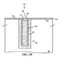
- a silicon dioxide layer 145has been formed on the sides and bottom of trench 140 .
- Silicon dioxide layer 145is formed by an oxidation processes. Because silicon dioxide grows in both directions from top surface 105 immediately adjacent to trench 140 , cusps 150 are formed in barrier layer 110 around the perimeter of trench 140 .
- silicon dioxide layer 145is formed by a wet oxidation using H 2 O at a temperature between about 1000° C. and about 1200° C. at room pressure (i.e., one atm).
- silicon dioxide layer 145is formed by a dry oxidation using O 2 a temperature of between about 1000° C. and about 1200° C.) at room pressure.
- silicon dioxide layer 145is formed in a high pressure (i.e., greater than one atm) using O 2 or H 2 O at a temperature between about 500° C. and about 800° C. Silicon dioxide layer 145 has a thickness of T 1 . Since silicon dioxide layer 145 is formed by oxidation, about half the thickness of the silicon dioxide layer is formed by consumption of silicon wherein about half the oxide growth is into the substrate from the original ( FIG. 1E ) sidewall of trench 140 and about half the oxide growth is into the trench from the original sidewall of the trench. A layer of silicon about (T 1 )/2 in thickness on the sidewalls and bottom of trench 140 has been consumed. Trench 140 now has a reduced with of W 4 so W 1 (see FIG.
- T 1Eis about equal to W 4 +T 1 .
- T 1is between 0.1 micron and about 1 micron and W 4 is between about 0.8 microns and about 4.8 microns.
- T 1is at least at least about 0.5 microns.
- a feature of the embodiments of the present inventionis to form silicon dioxide layer 145 with thickness variation of less than about 10% between thinnest and thickest (measured in a direction perpendicular to the sidewalls of the trench) regions of the silicon dioxide layer on the sidewalls of the trench which is not achievable in current CMOS compatible trench technology.
- a feature of the embodiments of the present inventionis the ability to form silicon dioxide layer 145 with a thickness of about 0.5 micron or greater which is not achievable in current CMOS compatible trench technology.
- a feature of the embodiments of the present inventionis to form silicon dioxide layer 145 with thickness variation of less than about 10% between thinnest and thickest (measured in a direction perpendicular to the sidewalls of the trench) regions of the oxide on the sidewalls of the trench and to form silicon dioxide layer 145 with a thickness of about 0.5 micron or greater which is not achievable in current CMOS compatible trench technology.
- Hardmask layer 155may comprise any the same materials and combination of materials as described supra for oxidation barrier 110 (see FIG. 1A ). For illustrative purposes, hardmask layer 155 will be illustrated in subsequent drawing figures described infra.
- a fill layer 160is deposited on hardmask layer 155 (if present, otherwise on barrier layer 110 , see FIG. 1H ).
- fill layer 160comprises polysilicon. Fill layer 160 fills all remaining space in trench 140 . If the largest distance between any layers on the sidewalls of trench 140 is B and the thickness of fill layer 160 is C, then C may be about 1.5 times B to ensure trench 140 is completely filled the top with fill layer 160 .
- a chemical-mechanical-polish(CMP) is performed so a top surface 165 of fill layer 160 in trench 140 is coplanar with a top surface 170 of hardmask layer 155 .
- CMPchemical-mechanical-polish
- an fill layer recess etchis performed to recess top surface 175 of fill layer 160 a distance R below top surface 105 of substrate 100 .
- the fill recess etchis a reactive ion etch (RIE).
- Ris between about 50 nm and about 500 nm.
- an optional dielectric cap 180is formed in trench 140 , filling the recess formed in FIG. 1L .
- a top surface 185 of cap 180is coplanar with top surface 170 of hardmask layer 155 .
- cap 180is formed by a chemical-vapor-deposition (CVD) of silicon dioxide, followed by a CMP. For illustrative purposes, cap 180 will be illustrated in subsequent drawing figures described infra.
- CVDchemical-vapor-deposition
- the structure in FIG. 1Mmay be considered a precursor through silicon via 190 .
- the through silicon viais completed in steps illustrated in FIGS. 2A through 2G and described infra in conjunction with fabrication of CMOS devices and devices compatible with CMOS technology.
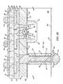
- FIGS. 2A through 2Hare cross-sectional views illustrating further fabrication steps of a through silicon via integrated with fabrication of CMOS integrated circuit devices and wiring according to embodiments of the present invention.
- FIG. 2Anormal fabrication of an integrated circuit is started using substrate 100 having one or more precursor through. silicon vias 190 .
- a field effect transistor (FET) 200has been fabricated.
- FET 200includes source/drains 205 formed in a well 210 and separate by channel region 215 under a gate electrode 220 .
- Gate electrode 215is separated from channel region by a gate dielectric 225 .
- Dielectric sidewall spacershave been formed on the sidewalls of gate electrode 220 .
- Source/drains 205 and well 210are formed in substrate 100 .
- Dielectric trench isolation 235abuts the perimeter of well 210 and abuts source/drains 205 .
- Gate dielectric 225is formed on top surface 105 of substrate 100 and gate electrode 220 and spacers 230 are formed above top surface 105 .
- Metal silicide contacts(not shown) are formed on the exposed surfaces of source/drains 205 and gate electrode 220 .
- FET 200is an example of a CMOS device that may be fabricated at this point in the process.
- CMOS devicesor CMOS compatible (i.e., may be fabricated using CMOS process technology) include, bipolar transistors (including SiGe transistors), diodes, capacitors, trench capacitors, and resistors (including polysilicon and metal resistors).
- a dielectric passivation layer 240is deposited on hardmask layer 155 , trench isolation 235 and exposed portions of FET 200 .
- dielectric layer 240is silicon dioxide.
- passivation layer 240is formed by CVD using tetraethoxysilane (TEOS) (i.e., to form TEOS oxide).
- passivation layer 240is formed by high pressure (greater than 1 atm) plasma deposition of oxide using silane and/or silane derivatives (i.e., to form an HDP oxide).
- metal contacts 245 to source/drains 205 and gate electrode 220are formed through passivation layer 240 .
- contacts 245comprise tungsten.
- Metal contacts 245have been formed using a damascene process.
- a damascene processis one in which wire trenches or via openings are formed in a dielectric layer, an electrical conductor of sufficient thickness to fill the trenches is deposited on a top surface of the dielectric, and a chemical-mechanical-polish (CMP) process is performed to remove excess conductor and make the surface of the conductor co-planar with the surface of the dielectric layer to form damascene wires (or damascene vias).
- CMPchemical-mechanical-polish
- a photolithographic/RIE processis used to form an opening 250 through passivation layer 140 and hardmask layer 155 over precursor through silicon via 190 .
- dielectric cap 180(see FIG. 2B ) is removed during this process as well as upper regions of hardmask layer 155 and silicon dioxide layer 145 exposed in opening 250 .
- fill layer 160is removed from trench 140 .
- a polysilicon Bosch etch processselective to the materials of hardmask layer 155 and silicon dioxide layer 145 is used to remove fill layer 160 (see FIG. 2C ).
- a wet etch using aqueous TMAH or aqueous ammonium hydroxideis used to 160 (see FIG. 2C ).
- a polysilicon Bosch etch processselective to the materials of hardmask layer 155 and silicon dioxide layer 145 is used to remove fill layer 160 (see FIG. 2C ) followed by a wet cleanup up etch in aqueous tetramethylammonium hydroxide (TMAH) or aqueous ammonium hydroxide.
- TMAHtetramethylammonium hydroxide
- an electrically conductive core 255completely fills the space in trench 140 and opening 150 .
- a top surface of core 255is coplanar with a top surface of passivation layer 240 .
- Core 255has been formed using a damascene process.
- core 255comprises a metal.
- core 255comprises a refractory metal.
- Refractory metalsare a class of metals extraordinarily resistant to heat, wear, and corrosion. The five refractory metals are: Tungsten (W), Molybdenum (Mo), Niobium (Nb), Tantalum (Ta), and Rheilium (Re).
- core 255comprises tungsten, tantalum or a combination thereof.
- core 255comprises copper or a combination of copper and tantalum. In one example, core 255 comprises doped polysilicon. This completes fabrication of an integrated circuit through what is termed the fiont-end-of-line (FEOL) operations or simply through FEOL. Core 255 includes an integral contact region 257 in passivation layer 240 .
- FEOLfiont-end-of-line
- a first wiring level 255includes dual damascene wires 260 formed in an interlevel dielectric (ILD) layer 260 .
- ILDinterlevel dielectric
- a dual-damascene processis one in which via openings are formed through the entire thickness of a dielectric layer followed by formation of trenches part of the way through the dielectric layer in any given cross-sectional view. All via openings are intersected by integral wire trenches above and by a wire trench below, but not all trenches need intersect a via opening.
- An electrical conductor of sufficient thickness to fill the trenches and via openingis deposited on a top surface of the dielectric and a CMP process is performed to make the surface of the conductor in the trench co-planar with the surface the dielectric layer to form dual-damascene wires and dual-damascene wires having integral dual-damascene vias.
- the trenchis formed first followed by forming the via opening.
- wires 265may be formed using a single damascene processes for vias and a single damascene process for wires (but ILD 255 would comprise two dielectric layers).
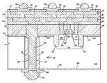
- a second wiring level 270includes dual damascene wires 275 formed in an ILD layer 280 . This completes BEOL fabrication of the integrated circuit.
- FIG. 2Ga backside grinding and/or CMP has been performed to thin substrate 100 and expose a bottom surface 290 of core 255 and complete fabrication of through silicon via 285 .
- Bottom surface 190 of core 255is coplanar with a bottom surface 295 of substrate 100 .
- Various interconnect structuresmay now be made to wires 275 and through silicon via 285 such as forming solder bump connections to core 290 and wires 275 . Examples of such interconnect structures are illustrated in FIG. 2H .
- a dielectric bottom passivation layer 300is formed on bottom surface 295 of substrate 100 .
- An electrically conductive bottom pad 305contacts core 255 through an opening in bottom passivation layer 300 over through silicon via 295 .
- a bottom solder bump 310is formed on bottom pad 305 .
- Electrically conductive top pads 325contacts wires 275 through openings in a top passivation layer 315 over through wires 275 .
- Top solder bumps 330are formed on top pads 325 . While a single through via 285 is connected to pad 305 , two or more through silicon vias may be connected to pad 305 and thus share a single bottom interconnection.
- fabrication of a through wafer viacomprised the steps of (1) forming a through silicon via precursor structure prior to FEOL, (2) modifying the through silicon via precursor structure by adding a core conductor during FEOL, and (3) completing the through silicon via after BEOL.
- the embodiments of the present inventionprovide through silicon vias and methods of fabricating through silicon vias that are compatible with CMOS technology and having superior insulator thickness from the top surface of the integrated circuit chip to the bottom surface of the integrated circuit then currently obtainable in the industry.
- the description of the embodiments of the present inventionis given above for the understanding of the present invention. It will be understood that the invention is not limited to the particular embodiments described herein, but is capable of various modifications, rearrangements and substitutions as will now become apparent to those skilled in the art without departing from the scope of the invention. Therefore, it is intended that the following claims cover all such modifications and changes as fall within the true spirit and scope of the invention.
Landscapes
- Engineering & Computer Science (AREA)
- Computer Hardware Design (AREA)
- Microelectronics & Electronic Packaging (AREA)
- Power Engineering (AREA)
- Physics & Mathematics (AREA)
- Condensed Matter Physics & Semiconductors (AREA)
- General Physics & Mathematics (AREA)
- Manufacturing & Machinery (AREA)
- Internal Circuitry In Semiconductor Integrated Circuit Devices (AREA)
- Metal-Oxide And Bipolar Metal-Oxide Semiconductor Integrated Circuits (AREA)
Abstract
Description
- The present invention relates to the field of integrated circuits; more specifically, it relates to through it relates to through silicon vias for use in integrated circuit chips and the method of fabricating through silicon vias.
- To increase the density of devices using integrated circuit chips it is desirable to allow interconnections to be made to both the top and bottom surfaces of the integrated circuit chip. This requires formation of through silicon vias from the top to the bottom surface of the integrated chip that are compatible with complementary metal oxide silicon (CMOS) technology. Many existing through via schemes are either difficult to integrate into CMOS fabrication processes or result in unacceptable degradation of signals propagating from/to the front surface of the integrated circuit chip to/from the bottom surface of the integrated circuit chip. Accordingly, there exists a need in the art to overcome the deficiencies and limitations described hereinabove.
- A first aspect of the present invention is a method, comprising: (a) forming a trench in a silicon substrate, the trench open to a top surface of the substrate; (b) forming a silicon dioxide layer on sidewalls of the trench, the silicon dioxide layer not filling the trench; (c) filling remaining space in the trench with polysilicon; after (c), (d) fabricating at least a portion of a CMOS device in the substrate; (e) removing the polysilicon from the trench, the dielectric layer remaining on the sidewalls of the trench; (f) re-filling the trench with an electrically conductive core; and after (f), (g) forming one or more wiring layers over the top surface of the substrate, a wire of a wiring level of the one or more wiring levels closet to the substrate contacting a top surface of the conductive core.
- A second aspect of the present invention is a method, comprising: (a) forming an oxidation barrier layer on a top surface of a silicon substrate and forming an opening in the barrier layer, a region of the top surface of the substrate exposed in a bottom of the opening; (b) forming a trench in the silicon substrate where the substrate is not protected by the barrier layer, the trench open to a top surface of the substrate; (c) forming a silicon dioxide layer on sidewalls of the trench, the silicon dioxide layer not filling the trench; (d) removing the oxidation barrier layer; (e) forming a hardmask layer on the top surface of the substrate and all exposed surfaces of the silicon dioxide layer; (f) filling remaining space in the trench with polysilicon after which a top surface of the polysilicon is coplanar with a top surface of the hardmask layer; after (f), (g) forming a source, drain and channel region of a field effect transistor in the substrate, a gate dielectric on the channel region and a gate electrode on the gate dielectric; (h) forming a passivation layer over the hardmask layer and the field effect transistor; (i) forming metal contacts to respective the source, the drain and the gate electrode of the field effect transistor through the passivation layer, top surfaces of the metal contacts coplanar with a top surface of the passivation layer; (j) forming an opening in the passivation layer over the trench and removing the polysilicon from the trench, the dielectric layer and the hardmask layer remaining on the sidewalls of the trench, (k) re-filling the trench with an electrically conductive core, the dielectric layer and the hardmask layer remaining on the sidewalls of the trench, a top surface of the core coplanar with the top surface of the passivation layer; and after (k), (l) forming one or more wiring layers over the passivation layer, a wire of a wiring level of the one or more wiring levels closet to the substrate contacting the top surface of the conductive core.
- A third aspect of the present invention is a structure comprising: a trench in a silicon substrate; a silicon dioxide layer on sidewalls of the trench, the silicon dioxide layer not filling the trench, the silicon dioxide layer having a thickness variation of less than about 10% between thinnest and thickest regions of the silicon dioxide layer on the sidewalls of the trench; an electrically conductive core filling remaining space in the trench
- at least a portion of a CMOS device in the substrate; and one or more wiring layers over the top surface of the substrate, a wire of a wiring level of the one or more wiring levels closet to the substrate contacting a top surface of the conductive core.
- A fourth aspect of the present invention is a structure, comprising: a trench in a silicon substrate; a silicon dioxide layer on sidewalls of the trench, the silicon dioxide layer not filling the trench; a dielectric layer on the top surface of the substrate and on the silicon dioxide layer, the dielectric layer not filling the trench; an electrically conductive core filling remaining space in the trench, a source, drain and channel region of a field effect transistor in the substrate, a gate dielectric on the channel region and a gate electrode on the gate dielectric; a passivation layer over dielectric layer and the field effect transistor; the core extending through the passivation layer, a top surface of the core coplanar with the top surface of the passivation layer; metal contacts to respective the source, the drain and the gate electrode of the field effect transistor through the passivation layer, top surfaces of the metal contacts coplanar with a top surface of the passivation layer; and one or more wiring layers over the passivation layer, a wire of a wiring level of the one or more wiring levels closet to the substrate contacting the top surface of the conductive core.
- The features of the invention are set forth in the appended claims. The invention itself, however, will be best understood by reference to the following detailed description of an illustrative embodiment when read in conjunction with the accompanying drawings, wherein:
FIGS. 1A through 1M are cross-sectional views illustrating initial fabrication steps of a silicon through via according to embodiments of the present invention; andFIGS. 2A through 2H are cross-sectional views illustrating further fabrication steps of a through silicon via integrated with fabrication of CMOS integrated circuit devices and wiring according to embodiments of the present invention.FIGS. 1A through 1M are cross-sectional views illustrating initial fabrication steps of a silicon through via according to embodiments of the present invention. InFIG. 1A , a single-crystal silicon substrate 100 has atop surface 105. In one example,substrate 100 has a <100> crystal alignment relative totop surface 105. In one example,substrate 100 is doped P-type. Formed ontop surface 105 ofsubstrate 100 is abarrier layer 110. In one example,barrier layer 110 comprises two or more individual layers. In one example and as illustrated inFIG. 1A ,barrier layer 110 consists of afirst layer 115 onsubstrate 100 andsecond layer 120 on the first layer. In one example,first layer 115 is silicon dioxide and is between about 5 nm and about 20 nm thick andsecond layer 120 is silicon nitride and is between about 100 nm and about 30 nm thick. In one example,barrier layer 110 comprises one or more of a layer of silicon dioxide, a layer of silicon nitride and a layer of silicon carbide. One purpose ofbarrier layer 110 is to act as a silicon oxidation barrier (i.e., a diffusion barrier for oxygen (as O, O2or O3), hydrogen/oxygen compounds (e.g. H2O), and other oxygen containing compounds (e.g., NO, N2O)) for subsequent processing steps. Thus at least one layer ofbarrier layer 110 consists of a material that is an oxidation barrier.Barrier layer 110 also needs to be thick enough so if its surface oxidizes, there is enough thickness of material left to still act as an oxygen (or water) diffusion barrier. For illustrative purposes,first layer 115 andsecond layer 120 will be illustrated in subsequent drawing figures described infra.- In
FIG. 1B , aphotoresist layer 125 is formed onbarrier layer 110 and an opening130 photolithographically formed in the photoresist layer to expose the pad dielectric in the bottom of the opening. - A photolithographic process is one in which a photoresist layer is applied to a surface, the photoresist layer exposed to actinic radiation through a patterned photomask and the exposed photoresist layer developed to form a patterned photoresist layer. When the photoresist layer comprises positive photoresist, the developer dissolves the regions of the photoresist exposed to the actinic radiation and does not dissolve the regions where the patterned photomask blocked (or greatly attenuated the intensity of the radiation) from impinging on the photoresist layer. When the photoresist layer comprises negative photoresist, the developer does not dissolve the regions of the photoresist exposed to the actinic radiation and does dissolve the regions where the patterned photomask blocked (or greatly attenuated the intensity of the radiation) from impinging on the photoresist layer. After further processing (e.g., an etch or an ion implantation), the patterned photoresist is removed. The photoresist layer may optionally be baked at one or more of prior to exposure to actinic radiation, between exposure to actinic radiation and development, after development.
- In
FIG. 1C , anopening 135 is etched throughbarrier layer 110 where the barrier layer is exposed in opening130 ofphotoresist layer 125.Top surface 105 ofsubstrate 100 is exposed in the bottom of opening135. In one example, opening135 is formed by a reactive ion etch (RIE) process. - In
FIG. 1D , atrench 140 is etched intosubstrate 100 in opening135 inbarrier layer 110. In one example,trench 140 is etched using a RIE process. One example of a suitable RIE process foretching trench 140 is known in the industry as the Bosch process (also known as pulsed or time-multiplexed plasma etching process). - In
FIG. 1E photoresist layer 135 is removed (seeFIG. 1D ). This may be done by dry stripping ashing (e.g., etching the photoresist layer in an oxygen plasma), wet stripping in an acid solution, or a combination of both dry and wet stripping.Trench 140 extends from top surface105 a distance D intosubstrate 100 and has a substantially uniform (i.e., within about plus or minus 10% of W1) with essentiallystraight sidewalls 141 at an angle A measured relative totop surface 105 ofsubstrate 100. In one example A is between about 85° and about 95°. In one example A is between about 88° and about 92°. As illustrated inFIG. 1E , A is equal to about 90°. It is advantageous that A be as close to 90° as possible. In one example D is between about 20 microns and about 200 microns and W1 is between about 1 micron and about 5 microns. Width is defined as a distance between the two closest and opposite sidewalls of a trench measured in a plane parallel to top surface of the substrate. For example, in a rectangular trench with straight sides, width is measured between and perpendicular to the long sides and a single width value is obtained. For example, in a rectangular trench with tapered sides, width is measured between and perpendicular to the long sides, however the width value will vary depending on which plane parallel to the top surface of the substrate the width is measured in but is still measured between the closest opposite sidewalls. FIG. 1F illustrates a first alternative shaped trench. InFIG. 1F atrench 140A has a width W1 at the top of the trench and a width W2 at the bottom of the trench. W1 is greater than W2. InFIG. 1F , sidewalls142 uniformly taper inward at angle A. As illustrated inFIG. 1F , A is greater than 90°.FIG. 1G illustrates a second alternative shaped trench. InFIG. 1G atrench 140B has a width W1 at the top of the trench and a width W3 at the bottom of the trench. W3 is greater than W1. InFIG. 1G ,trench 140B has outwardly taperingsidewalls 143 and a bulbus bottom144. As illustrated inFIG. 1G , A is less than 90°. For illustrative purposes,trench 140 ofFIG. 1E will be illustrated in subsequent drawing figures described infra.- In
FIG. 1H , asilicon dioxide layer 145 has been formed on the sides and bottom oftrench 140.Silicon dioxide layer 145 is formed by an oxidation processes. Because silicon dioxide grows in both directions fromtop surface 105 immediately adjacent to trench140,cusps 150 are formed inbarrier layer 110 around the perimeter oftrench 140. In one example,silicon dioxide layer 145 is formed by a wet oxidation using H2O at a temperature between about 1000° C. and about 1200° C. at room pressure (i.e., one atm). In one example,silicon dioxide layer 145 is formed by a dry oxidation using O2a temperature of between about 1000° C. and about 1200° C.) at room pressure. In one example,silicon dioxide layer 145 is formed in a high pressure (i.e., greater than one atm) using O2or H2O at a temperature between about 500° C. and about 800° C.Silicon dioxide layer 145 has a thickness of T1. Sincesilicon dioxide layer 145 is formed by oxidation, about half the thickness of the silicon dioxide layer is formed by consumption of silicon wherein about half the oxide growth is into the substrate from the original (FIG. 1E ) sidewall oftrench 140 and about half the oxide growth is into the trench from the original sidewall of the trench. A layer of silicon about (T1)/2 in thickness on the sidewalls and bottom oftrench 140 has been consumed. Trench140 now has a reduced with of W4 so W1 (seeFIG. 1E ) is about equal to W4+T1. In one example T1 is between 0.1 micron and about 1 micron and W4 is between about 0.8 microns and about 4.8 microns. In one example T1 is at least at least about 0.5 microns. - A feature of the embodiments of the present invention is to form
silicon dioxide layer 145 with thickness variation of less than about 10% between thinnest and thickest (measured in a direction perpendicular to the sidewalls of the trench) regions of the silicon dioxide layer on the sidewalls of the trench which is not achievable in current CMOS compatible trench technology. A feature of the embodiments of the present invention is the ability to formsilicon dioxide layer 145 with a thickness of about 0.5 micron or greater which is not achievable in current CMOS compatible trench technology. A feature of the embodiments of the present invention is to formsilicon dioxide layer 145 with thickness variation of less than about 10% between thinnest and thickest (measured in a direction perpendicular to the sidewalls of the trench) regions of the oxide on the sidewalls of the trench and to formsilicon dioxide layer 145 with a thickness of about 0.5 micron or greater which is not achievable in current CMOS compatible trench technology. - In
FIG. 1I , optionally barrier layer110 (seeFIG. 1H ) is removed and ahardmask layer 155 is deposited overtop surface 105 ofsubstrate 100 and all exposed surfaces ofsilicon dioxide layer 145.Hardmask layer 155 may comprise any the same materials and combination of materials as described supra for oxidation barrier110 (seeFIG. 1A ). For illustrative purposes,hardmask layer 155 will be illustrated in subsequent drawing figures described infra. - In
FIG. 1J , afill layer 160 is deposited on hardmask layer155 (if present, otherwise onbarrier layer 110, seeFIG. 1H ). In one example, filllayer 160 comprises polysilicon.Fill layer 160 fills all remaining space intrench 140. If the largest distance between any layers on the sidewalls oftrench 140 is B and the thickness offill layer 160 is C, then C may be about 1.5 times B to ensuretrench 140 is completely filled the top withfill layer 160. - In
FIG. 1K , a chemical-mechanical-polish (CMP) is performed so atop surface 165 offill layer 160 intrench 140 is coplanar with atop surface 170 ofhardmask layer 155. Thus,hardmask layer 155 also acts as a polish stop layer. - In
FIG. 1L , an fill layer recess etch is performed to recesstop surface 175 of fill layer160 a distance R belowtop surface 105 ofsubstrate 100. In one example, the fill recess etch is a reactive ion etch (RIE). In one, example, R is between about 50 nm and about 500 nm. If the optional fill recess etch is performed then inFIG. 1M , anoptional dielectric cap 180 is formed intrench 140, filling the recess formed inFIG. 1L . Atop surface 185 ofcap 180 is coplanar withtop surface 170 ofhardmask layer 155. In one example,cap 180 is formed by a chemical-vapor-deposition (CVD) of silicon dioxide, followed by a CMP. For illustrative purposes,cap 180 will be illustrated in subsequent drawing figures described infra. - The structure in
FIG. 1M may be considered a precursor through silicon via190. The through silicon via is completed in steps illustrated inFIGS. 2A through 2G and described infra in conjunction with fabrication of CMOS devices and devices compatible with CMOS technology. FIGS. 2A through 2H are cross-sectional views illustrating further fabrication steps of a through silicon via integrated with fabrication of CMOS integrated circuit devices and wiring according to embodiments of the present invention. InFIG. 2A , normal fabrication of an integrated circuit is started usingsubstrate 100 having one or more precursor through.silicon vias 190. InFIG. 2A , a field effect transistor (FET)200 has been fabricated.FET 200 includes source/drains205 formed in a well210 and separate bychannel region 215 under agate electrode 220.Gate electrode 215 is separated from channel region by agate dielectric 225. Dielectric sidewall spacers have been formed on the sidewalls ofgate electrode 220. Source/drains205 and well210 are formed insubstrate 100.Dielectric trench isolation 235 abuts the perimeter of well210 and abuts source/drains205.Gate dielectric 225, is formed ontop surface 105 ofsubstrate 100 andgate electrode 220 andspacers 230 are formed abovetop surface 105. Metal silicide contacts (not shown) are formed on the exposed surfaces of source/drains205 andgate electrode 220.FET 200 is an example of a CMOS device that may be fabricated at this point in the process. Other types of CMOS devices or CMOS compatible (i.e., may be fabricated using CMOS process technology) include, bipolar transistors (including SiGe transistors), diodes, capacitors, trench capacitors, and resistors (including polysilicon and metal resistors). After fabrication of FET200 (and/or FETs and other devices) adielectric passivation layer 240 is deposited onhardmask layer 155,trench isolation 235 and exposed portions ofFET 200. In one example,dielectric layer 240 is silicon dioxide. In one example,passivation layer 240 is formed by CVD using tetraethoxysilane (TEOS) (i.e., to form TEOS oxide). In one example,passivation layer 240 is formed by high pressure (greater than 1 atm) plasma deposition of oxide using silane and/or silane derivatives (i.e., to form an HDP oxide).- In
FIG. 2B ,metal contacts 245 to source/drains205 andgate electrode 220 are formed throughpassivation layer 240. In one example,contacts 245 comprise tungsten.Metal contacts 245 have been formed using a damascene process. - A damascene process is one in which wire trenches or via openings are formed in a dielectric layer, an electrical conductor of sufficient thickness to fill the trenches is deposited on a top surface of the dielectric, and a chemical-mechanical-polish (CMP) process is performed to remove excess conductor and make the surface of the conductor co-planar with the surface of the dielectric layer to form damascene wires (or damascene vias). When only a trench and a wire (or a via opening and a via) is formed the process is called single-damascene. The term wire is intended to include the term contact.
- In
FIG. 2C , a photolithographic/RIE process is used to form anopening 250 throughpassivation layer 140 andhardmask layer 155 over precursor through silicon via190. Note that dielectric cap180 (seeFIG. 2B ) is removed during this process as well as upper regions ofhardmask layer 155 andsilicon dioxide layer 145 exposed inopening 250. - In
FIG. 2D , fill layer160 (seeFIG. 2C ) is removed fromtrench 140. In a first example, a polysilicon Bosch etch process (selective to the materials ofhardmask layer 155 andsilicon dioxide layer 145 is used to remove fill layer160 (seeFIG. 2C ). In a second example, a wet etch using aqueous TMAH or aqueous ammonium hydroxide is used to160 (seeFIG. 2C ). In a third example, a polysilicon Bosch etch process (selective to the materials ofhardmask layer 155 andsilicon dioxide layer 145 is used to remove fill layer160 (seeFIG. 2C ) followed by a wet cleanup up etch in aqueous tetramethylammonium hydroxide (TMAH) or aqueous ammonium hydroxide. - In
FIG. 2E , an electricallyconductive core 255 completely fills the space intrench 140 andopening 150. A top surface ofcore 255 is coplanar with a top surface ofpassivation layer 240.Core 255 has been formed using a damascene process. In one example,core 255 comprises a metal. In one example,core 255 comprises a refractory metal. Refractory metals are a class of metals extraordinarily resistant to heat, wear, and corrosion. The five refractory metals are: Tungsten (W), Molybdenum (Mo), Niobium (Nb), Tantalum (Ta), and Rheilium (Re). In one example,core 255 comprises tungsten, tantalum or a combination thereof. In one example,core 255 comprises copper or a combination of copper and tantalum. In one example,core 255 comprises doped polysilicon. This completes fabrication of an integrated circuit through what is termed the fiont-end-of-line (FEOL) operations or simply through FEOL.Core 255 includes anintegral contact region 257 inpassivation layer 240. - In
FIG. 2F , fabrication of the integrated circuit is complete by the addition of one or more wiring levels during what is termed back-end-of line BEOL operations or simply BEOL. InFIG. 2F , two wiring levels have been added. Afirst wiring level 255 includes dualdamascene wires 260 formed in an interlevel dielectric (ILD)layer 260. - A dual-damascene process is one in which via openings are formed through the entire thickness of a dielectric layer followed by formation of trenches part of the way through the dielectric layer in any given cross-sectional view. All via openings are intersected by integral wire trenches above and by a wire trench below, but not all trenches need intersect a via opening. An electrical conductor of sufficient thickness to fill the trenches and via opening is deposited on a top surface of the dielectric and a CMP process is performed to make the surface of the conductor in the trench co-planar with the surface the dielectric layer to form dual-damascene wires and dual-damascene wires having integral dual-damascene vias. In some dual damascene processes the trench is formed first followed by forming the via opening.
- Alternatively,
wires 265 may be formed using a single damascene processes for vias and a single damascene process for wires (butILD 255 would comprise two dielectric layers). Asecond wiring level 270 includes dualdamascene wires 275 formed in anILD layer 280. This completes BEOL fabrication of the integrated circuit. - Subsequent to BEOL, further operations are performed. In
FIG. 2G , a backside grinding and/or CMP has been performed tothin substrate 100 and expose abottom surface 290 ofcore 255 and complete fabrication of through silicon via285.Bottom surface 190 ofcore 255 is coplanar with abottom surface 295 ofsubstrate 100. Various interconnect structures may now be made towires 275 and through silicon via285 such as forming solder bump connections tocore 290 andwires 275. Examples of such interconnect structures are illustrated inFIG. 2H . - In
FIG. 2H , InFIG. 2H a dielectricbottom passivation layer 300 is formed onbottom surface 295 ofsubstrate 100. An electrically conductivebottom pad 305contacts core 255 through an opening inbottom passivation layer 300 over through silicon via295. Abottom solder bump 310 is formed onbottom pad 305. Electrically conductivetop pads 325contacts wires 275 through openings in atop passivation layer 315 over throughwires 275. Top solder bumps330 are formed ontop pads 325. While a single through via285 is connected to pad305, two or more through silicon vias may be connected to pad305 and thus share a single bottom interconnection. Thus, fabrication of a through wafer via according to embodiments of the present invention comprised the steps of (1) forming a through silicon via precursor structure prior to FEOL, (2) modifying the through silicon via precursor structure by adding a core conductor during FEOL, and (3) completing the through silicon via after BEOL. - Thus the embodiments of the present invention provide through silicon vias and methods of fabricating through silicon vias that are compatible with CMOS technology and having superior insulator thickness from the top surface of the integrated circuit chip to the bottom surface of the integrated circuit then currently obtainable in the industry. The description of the embodiments of the present invention is given above for the understanding of the present invention. It will be understood that the invention is not limited to the particular embodiments described herein, but is capable of various modifications, rearrangements and substitutions as will now become apparent to those skilled in the art without departing from the scope of the invention. Therefore, it is intended that the following claims cover all such modifications and changes as fall within the true spirit and scope of the invention.
Claims (35)
Priority Applications (8)
| Application Number | Priority Date | Filing Date | Title |
|---|---|---|---|
| US12/188,228US8138036B2 (en) | 2008-08-08 | 2008-08-08 | Through silicon via and method of fabricating same |
| TW098125343ATWI515826B (en) | 2008-08-08 | 2009-07-28 | Through-layer and its manufacturing method |
| PCT/US2009/052643WO2010017162A1 (en) | 2008-08-08 | 2009-08-04 | Through silicon via and method of fabricating same |
| JP2011522155AJP5709265B2 (en) | 2008-08-08 | 2009-08-04 | How to make through-silicon vias |
| KR1020117004709AKR101546995B1 (en) | 2008-08-08 | 2009-08-04 | Through silicon via and method of fabricating same |
| EP09805415.8AEP2319075B1 (en) | 2008-08-08 | 2009-08-04 | Method of fabricating a through silicon via |
| US13/364,804US8637937B2 (en) | 2008-08-08 | 2012-02-02 | Through silicon via for use in integrated circuit chips |
| US14/046,414US8735251B2 (en) | 2008-08-08 | 2013-10-04 | Through silicon via and method of fabricating same |
Applications Claiming Priority (1)
| Application Number | Priority Date | Filing Date | Title |
|---|---|---|---|
| US12/188,228US8138036B2 (en) | 2008-08-08 | 2008-08-08 | Through silicon via and method of fabricating same |
Related Child Applications (1)
| Application Number | Title | Priority Date | Filing Date |
|---|---|---|---|
| US13/364,804DivisionUS8637937B2 (en) | 2008-08-08 | 2012-02-02 | Through silicon via for use in integrated circuit chips |
Publications (2)
| Publication Number | Publication Date |
|---|---|
| US20100032764A1true US20100032764A1 (en) | 2010-02-11 |
| US8138036B2 US8138036B2 (en) | 2012-03-20 |
Family
ID=41652107
Family Applications (3)
| Application Number | Title | Priority Date | Filing Date |
|---|---|---|---|
| US12/188,228Expired - Fee RelatedUS8138036B2 (en) | 2008-08-08 | 2008-08-08 | Through silicon via and method of fabricating same |
| US13/364,804Expired - Fee RelatedUS8637937B2 (en) | 2008-08-08 | 2012-02-02 | Through silicon via for use in integrated circuit chips |
| US14/046,414Expired - Fee RelatedUS8735251B2 (en) | 2008-08-08 | 2013-10-04 | Through silicon via and method of fabricating same |
Family Applications After (2)
| Application Number | Title | Priority Date | Filing Date |
|---|---|---|---|
| US13/364,804Expired - Fee RelatedUS8637937B2 (en) | 2008-08-08 | 2012-02-02 | Through silicon via for use in integrated circuit chips |
| US14/046,414Expired - Fee RelatedUS8735251B2 (en) | 2008-08-08 | 2013-10-04 | Through silicon via and method of fabricating same |
Country Status (6)
| Country | Link |
|---|---|
| US (3) | US8138036B2 (en) |
| EP (1) | EP2319075B1 (en) |
| JP (1) | JP5709265B2 (en) |
| KR (1) | KR101546995B1 (en) |
| TW (1) | TWI515826B (en) |
| WO (1) | WO2010017162A1 (en) |
Cited By (52)
| Publication number | Priority date | Publication date | Assignee | Title |
|---|---|---|---|---|
| US20100032811A1 (en)* | 2008-08-08 | 2010-02-11 | Hanyi Ding | Through wafer vias and method of making same |
| US20100032810A1 (en)* | 2008-08-08 | 2010-02-11 | Hanyi Ding | Through wafer vias and method of making same |
| US20100155940A1 (en)* | 2008-12-19 | 2010-06-24 | Renesas Technology Corp. | Semiconductor device and method of manufacturing the same |
| US20100270597A1 (en)* | 2009-04-24 | 2010-10-28 | Synopsys, Inc. | Method and apparatus for placing transistors in proximity to through-silicon vias |
| US20110057319A1 (en)* | 2009-09-09 | 2011-03-10 | International Business Machines Corporation | Arranging through silicon vias in ic layout |
| US20110227194A1 (en)* | 2010-03-22 | 2011-09-22 | Stmicroelectronics S.A. | Method for forming a three-dimensional structure of metal-insulator-metal type |
| US20110237068A1 (en)* | 2010-03-24 | 2011-09-29 | Stmicroelectronics Sa | Method for forming electric vias |
| EP2378548A1 (en) | 2010-04-19 | 2011-10-19 | Nanda Technologies GmbH | Methods of processing and inspecting semiconductor substrates |
| US20120038049A1 (en)* | 2008-12-16 | 2012-02-16 | Achim Trautmann | Component having a via, and a method for manufacturing such a component |
| US20120061827A1 (en)* | 2010-09-15 | 2012-03-15 | Elpida Memory, Inc. | Semiconductor device |
| WO2012144951A1 (en)* | 2011-04-21 | 2012-10-26 | Silex Microsystems Ab | A starting substrate for semiconductor engineering having substrate-through connections and a method for making same |
| FR2976120A1 (en)* | 2011-06-01 | 2012-12-07 | St Microelectronics Sa | METHOD FOR MANUFACTURING AN INTEGRATED CIRCUIT COMPRISING AT LEAST ONE COPLANAR WAVEGUIDE |
| WO2012151229A3 (en)* | 2011-05-05 | 2013-01-03 | International Business Machines Corporation | 3-d integration using multi stage vias |
| US20130015504A1 (en)* | 2011-07-11 | 2013-01-17 | Chien-Li Kuo | Tsv structure and method for forming the same |
| US20130033303A1 (en)* | 2011-02-21 | 2013-02-07 | Takashi Morimoto | Integrated circuit |
| US8394718B1 (en) | 2011-09-12 | 2013-03-12 | International Business Machines Corporation | Methods of forming self-aligned through silicon via |
| US20130093042A1 (en)* | 2010-07-12 | 2013-04-18 | Taiwan Semiconductor Manufacturing Company, Ltd. | TSV Formation Processes Using TSV-Last Approach |
| US20130134491A1 (en)* | 2011-11-30 | 2013-05-30 | International Business Machines Corporation | Polysilicon/metal contact resistance in deep trench |
| US8487425B2 (en) | 2011-06-23 | 2013-07-16 | International Business Machines Corporation | Optimized annular copper TSV |
| US8492903B2 (en) | 2011-06-29 | 2013-07-23 | International Business Machines Corporation | Through silicon via direct FET signal gating |
| US20130277854A1 (en)* | 2012-04-23 | 2013-10-24 | Globalfoundries Inc. | 3d integrated circuit system with connecting via structure and method for forming the same |
| US8637937B2 (en) | 2008-08-08 | 2014-01-28 | Ultratech, Inc. | Through silicon via for use in integrated circuit chips |
| US8786058B2 (en) | 2010-11-08 | 2014-07-22 | Samsung Electronics Co., Ltd. | Semiconductor devices and methods of manufacturing the same |
| US8791009B2 (en) | 2011-06-07 | 2014-07-29 | International Business Machines Corporation | Method of forming a through-silicon via utilizing a metal contact pad in a back-end-of-line wiring level to fill the through-silicon via |
| US8823090B2 (en) | 2011-02-17 | 2014-09-02 | International Business Machines Corporation | Field-effect transistor and method of creating same |
| US8841754B2 (en) | 2012-03-22 | 2014-09-23 | Samsung Electronics Co., Ltd. | Semiconductor devices with stress relief layers |
| US8847400B2 (en) | 2010-09-15 | 2014-09-30 | Ps4 Luxco S.A.R.L. | Semiconductor device, method for manufacturing the same, and data processing device |
| US8941222B2 (en) | 2010-11-11 | 2015-01-27 | Advanced Semiconductor Engineering Inc. | Wafer level semiconductor package and manufacturing methods thereof |
| US20150054172A1 (en)* | 2013-08-21 | 2015-02-26 | Kabushiki Kaisha Toshiba | Semiconductor device and method of manufacturing the same |
| US9029988B2 (en) | 2010-09-30 | 2015-05-12 | International Business Machines Corporation | Through silicon via in n+ epitaxy wafers with reduced parasitic capacitance |
| US20150145119A1 (en)* | 2013-11-27 | 2015-05-28 | Taiwan Semiconductor Manufacturing Co., Ltd. | Integrated Circuit And Fabricating Method Thereof |
| US20150162418A1 (en)* | 2013-12-10 | 2015-06-11 | Infineon Technologies Ag | Method for forming a semiconductor device |
| US20150179737A1 (en)* | 2013-12-19 | 2015-06-25 | Infineon Technologies Austria Ag | Method for Producing a Semiconductor Device Having a Beveled Edge Termination |
| US20160013191A1 (en)* | 2014-04-09 | 2016-01-14 | Nanya Technology Corp. | Capacitor and method of manufacturing the same |
| US9349611B2 (en) | 2010-03-22 | 2016-05-24 | Advanced Semiconductor Engineering, Inc. | Stackable semiconductor package and manufacturing method thereof |
| US9406562B2 (en) | 2011-01-13 | 2016-08-02 | GlobalFoundries, Inc. | Integrated circuit and design structure having reduced through silicon via-induced stress |
| US9406658B2 (en) | 2010-12-17 | 2016-08-02 | Advanced Semiconductor Engineering, Inc. | Embedded component device and manufacturing methods thereof |
| US9490212B2 (en) | 2009-04-23 | 2016-11-08 | Huilong Zhu | High quality electrical contacts between integrated circuit chips |
| US9558933B2 (en) | 2013-12-10 | 2017-01-31 | Infineon Technologies Ag | Method for forming a semiconductor device |
| US9646882B2 (en) | 2009-04-23 | 2017-05-09 | Huilong Zhu | High quality electrical contacts between integrated circuit chips |
| US9741817B2 (en)* | 2016-01-21 | 2017-08-22 | Tower Semiconductor Ltd. | Method for manufacturing a trench metal insulator metal capacitor |
| US9761481B2 (en)* | 2013-01-23 | 2017-09-12 | GlobalFoundries, Inc. | Integrated circuits and methods of forming the same with metal layer connection to through-semiconductor via |
| US9780052B2 (en)* | 2015-09-14 | 2017-10-03 | Micron Technology, Inc. | Collars for under-bump metal structures and associated systems and methods |
| US20170372961A1 (en)* | 2009-08-21 | 2017-12-28 | Micron Technology, Inc. | Vias and conductive routing layers in semiconductor substrates |
| GB2523500B (en)* | 2012-12-21 | 2018-04-11 | Intel Corp | Landing structure for through-silicon via |
| US20180158733A1 (en)* | 2016-08-04 | 2018-06-07 | Globalfoundries Inc. | Integrated ciurcuit product having a through-substrate-via (tsv) and a metallization layer that are formed after formation of a semiconductor device |
| US9997443B2 (en) | 2013-02-25 | 2018-06-12 | Infineon Technologies Ag | Through vias and methods of formation thereof |
| US10777462B2 (en) | 2016-08-10 | 2020-09-15 | Sony Corporation | Semiconductor integrated circuit |
| CN114464584A (en)* | 2020-11-10 | 2022-05-10 | 南亚科技股份有限公司 | Semiconductor element structure with bottle-shaped through silicon via and preparation method thereof |
| US20220359290A1 (en)* | 2021-05-08 | 2022-11-10 | Changxin Memory Technologies, Inc. | Semiconductor structure and manufacturing method thereof |
| US20230377881A1 (en)* | 2020-10-27 | 2023-11-23 | Taiwan Semiconductor Manufacturing Company, Ltd. | Strain relief trenches for epitaxial growth |
| EP4435844A1 (en)* | 2023-03-21 | 2024-09-25 | Samsung Electronics Co., Ltd. | Semiconductor device with stacked transistors and via structure |
Families Citing this family (29)
| Publication number | Priority date | Publication date | Assignee | Title |
|---|---|---|---|---|
| KR101374338B1 (en)* | 2007-11-14 | 2014-03-14 | 삼성전자주식회사 | semicondoctor device having through-via and method of forming the same |
| US8519473B2 (en) | 2010-07-14 | 2013-08-27 | Infineon Technologies Ag | Vertical transistor component |
| US9396997B2 (en) | 2010-12-10 | 2016-07-19 | Infineon Technologies Ag | Method for producing a semiconductor component with insulated semiconductor mesas |
| US9142665B2 (en) | 2010-12-10 | 2015-09-22 | Infineon Technologies Austria Ag | Semiconductor component with a semiconductor via |
| JP2012195514A (en) | 2011-03-17 | 2012-10-11 | Seiko Epson Corp | Substrate with element, infrared sensor, and through electrode formation method |
| JP2013004572A (en)* | 2011-06-13 | 2013-01-07 | Mitsubishi Electric Corp | Semiconductor device manufacturing method |
| KR20130053338A (en)* | 2011-11-15 | 2013-05-23 | 삼성전자주식회사 | Integrated circuit device having through silicon via structure |
| KR101931115B1 (en)* | 2012-07-05 | 2018-12-20 | 삼성전자주식회사 | Semiconductor device and method of forming the same |
| JP2014107304A (en)* | 2012-11-22 | 2014-06-09 | Renesas Electronics Corp | Semiconductor device and manufacturing method of the same |
| US9245790B2 (en)* | 2013-01-23 | 2016-01-26 | GlobalFoundries, Inc. | Integrated circuits and methods of forming the same with multiple embedded interconnect connection to same through-semiconductor via |
| US9123789B2 (en)* | 2013-01-23 | 2015-09-01 | United Microelectronics Corp. | Chip with through silicon via electrode and method of forming the same |
| US9343400B2 (en)* | 2013-03-13 | 2016-05-17 | Taiwan Semiconductor Manufacturing Company, Ltd. | Dual damascene gap filling process |
| US9431320B2 (en)* | 2013-03-15 | 2016-08-30 | Analog Devices, Inc. | Methods and structures to facilitate through-silicon vias |
| JP5982312B2 (en) | 2013-03-22 | 2016-08-31 | 株式会社東芝 | Semiconductor device |
| KR20140140390A (en)* | 2013-05-29 | 2014-12-09 | 삼성전자주식회사 | Methods for fabricating semicondctor devices having through electrodes |
| KR20170023643A (en) | 2015-08-24 | 2017-03-06 | 삼성전자주식회사 | Semiconductor device and method of manufacturing the same |
| KR102500813B1 (en)* | 2015-09-24 | 2023-02-17 | 삼성전자주식회사 | Semiconductor device and method for manufacturing the same |
| US10147682B2 (en)* | 2015-11-30 | 2018-12-04 | Taiwan Semiconductor Manufacturing Co., Ltd. | Structure for stacked logic performance improvement |
| US9768062B1 (en)* | 2016-06-16 | 2017-09-19 | Samsung Electronics Co., Ltd. | Method for forming low parasitic capacitance source and drain contacts |
| JP6697411B2 (en)* | 2017-03-29 | 2020-05-20 | キオクシア株式会社 | Method of manufacturing semiconductor device |
| KR101928421B1 (en) | 2017-08-18 | 2018-12-12 | 강일중 | Method for manufacturing perpendicularity laminating chip and multi chip package and Apparatus for multi chip package |
| KR20190044196A (en) | 2017-10-20 | 2019-04-30 | 삼성전자주식회사 | Semiconductor device and method for manufacturing the same |
| KR102589608B1 (en) | 2018-10-22 | 2023-10-16 | 삼성전자주식회사 | Image sensor and method of manufacturing the same |
| TWI714093B (en)* | 2019-05-21 | 2020-12-21 | 友達光電股份有限公司 | Array substrate |
| US12107050B2 (en) | 2020-08-28 | 2024-10-01 | Micron Technology, Inc. | Front end of line interconnect structures and associated systems and methods |
| US11862569B2 (en) | 2020-08-28 | 2024-01-02 | Micron Technology, Inc. | Front end of line interconnect structures and associated systems and methods |
| US11817305B2 (en) | 2020-08-28 | 2023-11-14 | Micron Technology, Inc. | Front end of line interconnect structures and associated systems and methods |
| US12106969B2 (en)* | 2021-03-18 | 2024-10-01 | International Business Machines Corporation | Substrate thinning for a backside power distribution network |
| WO2023228704A1 (en)* | 2022-05-27 | 2023-11-30 | ソニーセミコンダクタソリューションズ株式会社 | Semiconductor device, electronic device and production method |
Citations (37)
| Publication number | Priority date | Publication date | Assignee | Title |
|---|---|---|---|---|
| US4666556A (en)* | 1986-05-12 | 1987-05-19 | International Business Machines Corporation | Trench sidewall isolation by polysilicon oxidation |
| US4690729A (en)* | 1985-05-03 | 1987-09-01 | Texas Instruments Incorporated | Tapered trench process |
| US5933748A (en)* | 1996-01-22 | 1999-08-03 | United Microelectronics Corp. | Shallow trench isolation process |
| US5998292A (en)* | 1997-11-12 | 1999-12-07 | International Business Machines Corporation | Method for making three dimensional circuit integration |
| US6406934B1 (en)* | 2000-09-05 | 2002-06-18 | Amkor Technology, Inc. | Wafer level production of chip size semiconductor packages |
| US6836020B2 (en)* | 2003-01-22 | 2004-12-28 | The Board Of Trustees Of The Leland Stanford Junior University | Electrical through wafer interconnects |
| US20050248002A1 (en)* | 2004-05-07 | 2005-11-10 | Michael Newman | Fill for large volume vias |
| US20060001174A1 (en)* | 2004-06-30 | 2006-01-05 | Nec Electronics Corporation | Semiconductor device and method for manufacturing the same |
| US20060006539A1 (en)* | 2004-06-30 | 2006-01-12 | Nec Electronics Corporation | Semiconductor device and semiconductor module employing thereof |
| US7005388B1 (en)* | 2003-12-04 | 2006-02-28 | National Semiconductor Corporation | Method of forming through-the-wafer metal interconnect structures |
| US20060105496A1 (en)* | 2004-11-16 | 2006-05-18 | Chen Howard H | Device and method for fabricating double-sided SOI wafer scale package with through via connections |
| US7056813B2 (en)* | 2003-09-17 | 2006-06-06 | Intel Corporation | Methods of forming backside connections on a wafer stack |
| US20060118965A1 (en)* | 2004-12-02 | 2006-06-08 | Nec Electronics Corporation | Semiconductor device, semiconductor module employing thereof and method for manufacturing semiconductor device |
| US7071098B2 (en)* | 2004-02-20 | 2006-07-04 | Micron Technology, Inc. | Methods of fabricating interconnects for semiconductor components including a through hole entirely through the component and forming a metal nitride including separate precursor cycles |
| US20060154438A1 (en)* | 2005-01-11 | 2006-07-13 | Daisuke Kishimoto | Method for manufacturing semiconductor device with trenches in substrate surface |
| US20060197119A1 (en)* | 2004-04-29 | 2006-09-07 | International Business Machines Corporation | Method for forming suspended transmission line structures in back end of line processing |
| US20060214298A1 (en)* | 2005-03-24 | 2006-09-28 | Kun-Cheng Huang | Dummy via for reducing proximity effect and method of using the same |
| US20060275946A1 (en)* | 2005-05-04 | 2006-12-07 | Icemos Technology Corporation | Silicon Wafer Having Through-Wafer Vias |
| US20070045779A1 (en)* | 2005-09-01 | 2007-03-01 | Hiatt W M | Methods for forming through-wafer interconnects, intermediate structures so formed, and devices and systems having at least one solder dam structure |
| US20070048896A1 (en)* | 2005-08-30 | 2007-03-01 | International Business Machines Corporation | Conductive through via structure and process for electronic device carriers |
| US7224051B2 (en)* | 2003-03-31 | 2007-05-29 | Micron Technology, Inc. | Semiconductor component having plate and stacked dice |
| US20070190692A1 (en)* | 2006-01-13 | 2007-08-16 | Mete Erturk | Low resistance and inductance backside through vias and methods of fabricating same |
| US7259454B2 (en)* | 2004-08-20 | 2007-08-21 | Rohm Co., Ltd. | Semiconductor chip manufacturing method, semiconductor chip, semiconductor device manufacturing method, and semiconductor device |
| US20070197018A1 (en)* | 2004-07-23 | 2007-08-23 | Industrial Technology Research Institute | Wafer-leveled chip packaging structure and method thereof |
| US20070196948A1 (en)* | 2005-06-14 | 2007-08-23 | John Trezza | Stacked chip-based system and method |
| US7271491B1 (en)* | 2000-08-31 | 2007-09-18 | Micron Technology, Inc. | Carrier for wafer-scale package and wafer-scale package including the carrier |
| US7276787B2 (en)* | 2003-12-05 | 2007-10-02 | International Business Machines Corporation | Silicon chip carrier with conductive through-vias and method for fabricating same |
| US20080079131A1 (en)* | 2006-09-30 | 2008-04-03 | Sung Min Kim | Stack package and method for manufacturing the same |
| US20080099870A1 (en)* | 2006-08-10 | 2008-05-01 | Icemos Technology Corporation | Method of manufacturing a photodiode array with through-wafer vias |
| US20090215237A1 (en)* | 2006-08-28 | 2009-08-27 | Advanced Analogic Technologies, Inc. | Method of forming lateral trench MOSFET with direct trench polysilicon contact |
| US20090244954A1 (en)* | 2008-03-26 | 2009-10-01 | Cannon Ethan H | Structure and method for improving storage latch susceptibility to single event upsets |
| US20090267126A1 (en)* | 2008-04-25 | 2009-10-29 | Jer-Chyi Wang | Recess channel transistor |
| US20100032811A1 (en)* | 2008-08-08 | 2010-02-11 | Hanyi Ding | Through wafer vias and method of making same |
| US20100032808A1 (en)* | 2008-08-08 | 2010-02-11 | Hanyi Ding | Through wafer via and method of making same |
| US20100032810A1 (en)* | 2008-08-08 | 2010-02-11 | Hanyi Ding | Through wafer vias and method of making same |
| US7678696B2 (en)* | 2008-08-08 | 2010-03-16 | International Business Machines Corporation | Method of making through wafer vias |
| US20110012196A1 (en)* | 2007-03-28 | 2011-01-20 | Advanced Analogic Technologies, Inc. | Isolated drain-centric lateral MOSFET |
Family Cites Families (32)
| Publication number | Priority date | Publication date | Assignee | Title |
|---|---|---|---|---|
| US5608264A (en)* | 1995-06-05 | 1997-03-04 | Harris Corporation | Surface mountable integrated circuit with conductive vias |
| EP1001459B1 (en)* | 1998-09-09 | 2011-11-09 | Texas Instruments Incorporated | Integrated circuit comprising a capacitor and method |
| DE10014920C1 (en)* | 2000-03-17 | 2001-07-26 | Infineon Technologies Ag | Production of a trench capacitor comprises filling a trench with a filler, forming an insulating collar, removing the filler, forming a trenched plate using low pressure gas phase doping, etc. |
| US6329234B1 (en)* | 2000-07-24 | 2001-12-11 | Taiwan Semiconductor Manufactuirng Company | Copper process compatible CMOS metal-insulator-metal capacitor structure and its process flow |
| US6437386B1 (en)* | 2000-08-16 | 2002-08-20 | Fairchild Semiconductor Corporation | Method for creating thick oxide on the bottom surface of a trench structure in silicon |
| JP2002124517A (en)* | 2000-10-13 | 2002-04-26 | Sharp Corp | Semiconductor device and manufacturing method thereof |
| WO2004107434A1 (en)* | 2003-05-29 | 2004-12-09 | Nec Corporation | Wiring structure and method for producing same |
| JP2005243689A (en)* | 2004-02-24 | 2005-09-08 | Canon Inc | Semiconductor chip manufacturing method and semiconductor device |
| WO2005101476A1 (en)* | 2004-04-16 | 2005-10-27 | Japan Science And Technology Agency | Semiconductor element and semiconductor element manufacturing method |
| US7141855B2 (en) | 2004-04-27 | 2006-11-28 | Via Technologies, Inc. | Dual-thickness active device layer SOI chip structure |
| US7078814B2 (en)* | 2004-05-25 | 2006-07-18 | International Business Machines Corporation | Method of forming a semiconductor device having air gaps and the structure so formed |
| US7332408B2 (en)* | 2004-06-28 | 2008-02-19 | Micron Technology, Inc. | Isolation trenches for memory devices |
| US7223684B2 (en)* | 2004-07-14 | 2007-05-29 | International Business Machines Corporation | Dual damascene wiring and method |
| CN101048868B (en)* | 2004-08-20 | 2010-06-09 | 佐伊科比株式会社 | Method for manufacturing semiconductor device having three-dimensional stacked structure |
| US7396732B2 (en)* | 2004-12-17 | 2008-07-08 | Interuniversitair Microelektronica Centrum Vzw (Imec) | Formation of deep trench airgaps and related applications |
| US7786592B2 (en) | 2005-06-14 | 2010-08-31 | John Trezza | Chip capacitive coupling |
| US7838997B2 (en) | 2005-06-14 | 2010-11-23 | John Trezza | Remote chip attachment |
| US7989958B2 (en) | 2005-06-14 | 2011-08-02 | Cufer Assett Ltd. L.L.C. | Patterned contact |
| US7851348B2 (en) | 2005-06-14 | 2010-12-14 | Abhay Misra | Routingless chip architecture |
| US7781886B2 (en) | 2005-06-14 | 2010-08-24 | John Trezza | Electronic chip contact structure |
| DE102005029784A1 (en)* | 2005-06-24 | 2007-01-11 | Siemens Ag | Electronic assembly and method of making an electronic assembly |
| WO2007023947A1 (en) | 2005-08-26 | 2007-03-01 | Hitachi, Ltd. | Semiconductor device manufacturing method and semiconductor device |
| US7820997B2 (en)* | 2006-05-30 | 2010-10-26 | Macronix International Co., Ltd. | Resistor random access memory cell with reduced active area and reduced contact areas |
| US7879711B2 (en)* | 2006-11-28 | 2011-02-01 | Taiwan Semiconductor Manufacturing Co., Ltd. | Stacked structures and methods of fabricating stacked structures |
| JP4415984B2 (en)* | 2006-12-06 | 2010-02-17 | ソニー株式会社 | Manufacturing method of semiconductor device |
| US7863189B2 (en)* | 2007-01-05 | 2011-01-04 | International Business Machines Corporation | Methods for fabricating silicon carriers with conductive through-vias with low stress and low defect density |
| US8110464B2 (en)* | 2008-03-14 | 2012-02-07 | International Business Machines Corporation | SOI protection for buried plate implant and DT bottle ETCH |
| US7939876B2 (en)* | 2008-04-09 | 2011-05-10 | International Business Machines Corporation | Metallized conductive strap spacer for SOI deep trench capacitor |
| US7791124B2 (en)* | 2008-05-21 | 2010-09-07 | International Business Machines Corporation | SOI deep trench capacitor employing a non-conformal inner spacer |
| US8227310B2 (en)* | 2008-08-06 | 2012-07-24 | International Business Machines Corporation | Integrated circuits comprising an active transistor electrically connected to a trench capacitor by an overlying contact and methods of making |
| US8138036B2 (en) | 2008-08-08 | 2012-03-20 | International Business Machines Corporation | Through silicon via and method of fabricating same |
| JP2011009595A (en)* | 2009-06-29 | 2011-01-13 | Renesas Electronics Corp | Semiconductor device and method of manufacturing the same |
- 2008
- 2008-08-08USUS12/188,228patent/US8138036B2/ennot_activeExpired - Fee Related
- 2009
- 2009-07-28TWTW098125343Apatent/TWI515826B/ennot_activeIP Right Cessation
- 2009-08-04EPEP09805415.8Apatent/EP2319075B1/ennot_activeNot-in-force
- 2009-08-04KRKR1020117004709Apatent/KR101546995B1/ennot_activeExpired - Fee Related
- 2009-08-04WOPCT/US2009/052643patent/WO2010017162A1/enactiveApplication Filing
- 2009-08-04JPJP2011522155Apatent/JP5709265B2/ennot_activeExpired - Fee Related
- 2012
- 2012-02-02USUS13/364,804patent/US8637937B2/ennot_activeExpired - Fee Related
- 2013
- 2013-10-04USUS14/046,414patent/US8735251B2/ennot_activeExpired - Fee Related
Patent Citations (38)
| Publication number | Priority date | Publication date | Assignee | Title |
|---|---|---|---|---|
| US4690729A (en)* | 1985-05-03 | 1987-09-01 | Texas Instruments Incorporated | Tapered trench process |
| US4666556A (en)* | 1986-05-12 | 1987-05-19 | International Business Machines Corporation | Trench sidewall isolation by polysilicon oxidation |
| US5933748A (en)* | 1996-01-22 | 1999-08-03 | United Microelectronics Corp. | Shallow trench isolation process |
| US5998292A (en)* | 1997-11-12 | 1999-12-07 | International Business Machines Corporation | Method for making three dimensional circuit integration |
| US7271491B1 (en)* | 2000-08-31 | 2007-09-18 | Micron Technology, Inc. | Carrier for wafer-scale package and wafer-scale package including the carrier |
| US6406934B1 (en)* | 2000-09-05 | 2002-06-18 | Amkor Technology, Inc. | Wafer level production of chip size semiconductor packages |
| US6836020B2 (en)* | 2003-01-22 | 2004-12-28 | The Board Of Trustees Of The Leland Stanford Junior University | Electrical through wafer interconnects |
| US7224051B2 (en)* | 2003-03-31 | 2007-05-29 | Micron Technology, Inc. | Semiconductor component having plate and stacked dice |
| US7056813B2 (en)* | 2003-09-17 | 2006-06-06 | Intel Corporation | Methods of forming backside connections on a wafer stack |
| US7005388B1 (en)* | 2003-12-04 | 2006-02-28 | National Semiconductor Corporation | Method of forming through-the-wafer metal interconnect structures |
| US7276787B2 (en)* | 2003-12-05 | 2007-10-02 | International Business Machines Corporation | Silicon chip carrier with conductive through-vias and method for fabricating same |
| US7071098B2 (en)* | 2004-02-20 | 2006-07-04 | Micron Technology, Inc. | Methods of fabricating interconnects for semiconductor components including a through hole entirely through the component and forming a metal nitride including separate precursor cycles |
| US20060197119A1 (en)* | 2004-04-29 | 2006-09-07 | International Business Machines Corporation | Method for forming suspended transmission line structures in back end of line processing |
| US20050248002A1 (en)* | 2004-05-07 | 2005-11-10 | Michael Newman | Fill for large volume vias |
| US20060006539A1 (en)* | 2004-06-30 | 2006-01-12 | Nec Electronics Corporation | Semiconductor device and semiconductor module employing thereof |
| US20060001174A1 (en)* | 2004-06-30 | 2006-01-05 | Nec Electronics Corporation | Semiconductor device and method for manufacturing the same |
| US20070197018A1 (en)* | 2004-07-23 | 2007-08-23 | Industrial Technology Research Institute | Wafer-leveled chip packaging structure and method thereof |
| US7259454B2 (en)* | 2004-08-20 | 2007-08-21 | Rohm Co., Ltd. | Semiconductor chip manufacturing method, semiconductor chip, semiconductor device manufacturing method, and semiconductor device |
| US20060105496A1 (en)* | 2004-11-16 | 2006-05-18 | Chen Howard H | Device and method for fabricating double-sided SOI wafer scale package with through via connections |
| US20060118965A1 (en)* | 2004-12-02 | 2006-06-08 | Nec Electronics Corporation | Semiconductor device, semiconductor module employing thereof and method for manufacturing semiconductor device |
| US20060154438A1 (en)* | 2005-01-11 | 2006-07-13 | Daisuke Kishimoto | Method for manufacturing semiconductor device with trenches in substrate surface |
| US20060214298A1 (en)* | 2005-03-24 | 2006-09-28 | Kun-Cheng Huang | Dummy via for reducing proximity effect and method of using the same |
| US20060275946A1 (en)* | 2005-05-04 | 2006-12-07 | Icemos Technology Corporation | Silicon Wafer Having Through-Wafer Vias |
| US20070196948A1 (en)* | 2005-06-14 | 2007-08-23 | John Trezza | Stacked chip-based system and method |
| US20070048896A1 (en)* | 2005-08-30 | 2007-03-01 | International Business Machines Corporation | Conductive through via structure and process for electronic device carriers |
| US20070045779A1 (en)* | 2005-09-01 | 2007-03-01 | Hiatt W M | Methods for forming through-wafer interconnects, intermediate structures so formed, and devices and systems having at least one solder dam structure |
| US20070190692A1 (en)* | 2006-01-13 | 2007-08-16 | Mete Erturk | Low resistance and inductance backside through vias and methods of fabricating same |
| US20080099870A1 (en)* | 2006-08-10 | 2008-05-01 | Icemos Technology Corporation | Method of manufacturing a photodiode array with through-wafer vias |
| US20090215237A1 (en)* | 2006-08-28 | 2009-08-27 | Advanced Analogic Technologies, Inc. | Method of forming lateral trench MOSFET with direct trench polysilicon contact |
| US20080079131A1 (en)* | 2006-09-30 | 2008-04-03 | Sung Min Kim | Stack package and method for manufacturing the same |
| US20110012196A1 (en)* | 2007-03-28 | 2011-01-20 | Advanced Analogic Technologies, Inc. | Isolated drain-centric lateral MOSFET |
| US20090244954A1 (en)* | 2008-03-26 | 2009-10-01 | Cannon Ethan H | Structure and method for improving storage latch susceptibility to single event upsets |
| US20090267126A1 (en)* | 2008-04-25 | 2009-10-29 | Jer-Chyi Wang | Recess channel transistor |
| US20100032811A1 (en)* | 2008-08-08 | 2010-02-11 | Hanyi Ding | Through wafer vias and method of making same |
| US20100032808A1 (en)* | 2008-08-08 | 2010-02-11 | Hanyi Ding | Through wafer via and method of making same |
| US20100032810A1 (en)* | 2008-08-08 | 2010-02-11 | Hanyi Ding | Through wafer vias and method of making same |
| US7678696B2 (en)* | 2008-08-08 | 2010-03-16 | International Business Machines Corporation | Method of making through wafer vias |
| US8035198B2 (en)* | 2008-08-08 | 2011-10-11 | International Business Machines Corporation | Through wafer via and method of making same |
Cited By (103)
| Publication number | Priority date | Publication date | Assignee | Title |
|---|---|---|---|---|
| US8299566B2 (en) | 2008-08-08 | 2012-10-30 | International Business Machines Corporation | Through wafer vias and method of making same |
| US8518787B2 (en) | 2008-08-08 | 2013-08-27 | International Business Machines Corporation | Through wafer vias and method of making same |
| US8637937B2 (en) | 2008-08-08 | 2014-01-28 | Ultratech, Inc. | Through silicon via for use in integrated circuit chips |
| US20100032811A1 (en)* | 2008-08-08 | 2010-02-11 | Hanyi Ding | Through wafer vias and method of making same |
| US8384224B2 (en) | 2008-08-08 | 2013-02-26 | International Business Machines Corporation | Through wafer vias and method of making same |
| US8748308B2 (en) | 2008-08-08 | 2014-06-10 | International Business Machines Corporation | Through wafer vias and method of making same |
| US8735251B2 (en) | 2008-08-08 | 2014-05-27 | Ultratech, Inc. | Through silicon via and method of fabricating same |
| US20100032810A1 (en)* | 2008-08-08 | 2010-02-11 | Hanyi Ding | Through wafer vias and method of making same |
| US20120038049A1 (en)* | 2008-12-16 | 2012-02-16 | Achim Trautmann | Component having a via, and a method for manufacturing such a component |
| US8405190B2 (en)* | 2008-12-16 | 2013-03-26 | Robert Bosch Gmbh | Component having a silicon carbide coated via |
| US8816506B2 (en) | 2008-12-19 | 2014-08-26 | Tessera Advanced Technologies, Inc. | Semiconductor device and method of manufacturing the same |
| US9076700B2 (en) | 2008-12-19 | 2015-07-07 | Tessera Advanced Technologies, Inc. | Semiconductor device and method of manufacturing same |
| US20100155940A1 (en)* | 2008-12-19 | 2010-06-24 | Renesas Technology Corp. | Semiconductor device and method of manufacturing the same |
| US9318418B2 (en) | 2008-12-19 | 2016-04-19 | Tessera Advanced Technologies, Inc. | Semiconductor device and method of manufacturing same |
| US9691739B2 (en) | 2008-12-19 | 2017-06-27 | Tessera Advanced Technologies, Inc. | Semiconductor device and method of manufacturing same |
| US8106518B2 (en)* | 2008-12-19 | 2012-01-31 | Renesas Electronics Corporation | Semiconductor device and method of manufacturing the same |
| US9490212B2 (en) | 2009-04-23 | 2016-11-08 | Huilong Zhu | High quality electrical contacts between integrated circuit chips |
| US9646882B2 (en) | 2009-04-23 | 2017-05-09 | Huilong Zhu | High quality electrical contacts between integrated circuit chips |
| US8661387B2 (en) | 2009-04-24 | 2014-02-25 | Synopsys, Inc. | Placing transistors in proximity to through-silicon vias |
| US9003348B2 (en) | 2009-04-24 | 2015-04-07 | Synopsys, Inc. | Placing transistors in proximity to through-silicon vias |
| US8362622B2 (en)* | 2009-04-24 | 2013-01-29 | Synopsys, Inc. | Method and apparatus for placing transistors in proximity to through-silicon vias |
| US9275182B2 (en)* | 2009-04-24 | 2016-03-01 | Synopsys, Inc. | Placing transistors in proximity to through-silicon vias |
| US20100270597A1 (en)* | 2009-04-24 | 2010-10-28 | Synopsys, Inc. | Method and apparatus for placing transistors in proximity to through-silicon vias |
| US20170372961A1 (en)* | 2009-08-21 | 2017-12-28 | Micron Technology, Inc. | Vias and conductive routing layers in semiconductor substrates |
| US10600689B2 (en)* | 2009-08-21 | 2020-03-24 | Micron Technology, Inc. | Vias and conductive routing layers in semiconductor substrates |
| US20110057319A1 (en)* | 2009-09-09 | 2011-03-10 | International Business Machines Corporation | Arranging through silicon vias in ic layout |
| US8136084B2 (en) | 2009-09-09 | 2012-03-13 | International Business Machines Corporation | Arranging through silicon vias in IC layout |
| US9349611B2 (en) | 2010-03-22 | 2016-05-24 | Advanced Semiconductor Engineering, Inc. | Stackable semiconductor package and manufacturing method thereof |
| US20110227194A1 (en)* | 2010-03-22 | 2011-09-22 | Stmicroelectronics S.A. | Method for forming a three-dimensional structure of metal-insulator-metal type |
| US8609530B2 (en) | 2010-03-22 | 2013-12-17 | Stmicroelectronics S.A. | Method for forming a three-dimensional structure of metal-insulator-metal type |
| FR2958076A1 (en)* | 2010-03-24 | 2011-09-30 | St Microelectronics Sa | METHOD FOR FORMING ELECTRIC VIAS |
| US20110237068A1 (en)* | 2010-03-24 | 2011-09-29 | Stmicroelectronics Sa | Method for forming electric vias |
| US8298942B2 (en)* | 2010-03-24 | 2012-10-30 | Stmicroelectronics Sa | Method for forming electric vias |
| WO2011131349A1 (en) | 2010-04-19 | 2011-10-27 | Nanda Technologies Gmbh | Methods of processing and inspecting semiconductor substrates |
| US8460946B2 (en) | 2010-04-19 | 2013-06-11 | Nanda Technologies Gmbh | Methods of processing and inspecting semiconductor substrates |
| EP2378548A1 (en) | 2010-04-19 | 2011-10-19 | Nanda Technologies GmbH | Methods of processing and inspecting semiconductor substrates |
| US9343390B2 (en)* | 2010-07-12 | 2016-05-17 | Taiwan Semiconductor Manufacturing Company, Ltd. | TSV formation processes using TSV-last approach |
| US20130093042A1 (en)* | 2010-07-12 | 2013-04-18 | Taiwan Semiconductor Manufacturing Company, Ltd. | TSV Formation Processes Using TSV-Last Approach |
| US9847255B2 (en) | 2010-07-12 | 2017-12-19 | Taiwan Semiconductor Manufacturing Company, Ltd. | TSV formation processes using TSV-last approach |
| US9443790B2 (en) | 2010-09-15 | 2016-09-13 | Ps4 Luxco S.A.R.L. | Semiconductor device |
| US8847400B2 (en) | 2010-09-15 | 2014-09-30 | Ps4 Luxco S.A.R.L. | Semiconductor device, method for manufacturing the same, and data processing device |
| US20120061827A1 (en)* | 2010-09-15 | 2012-03-15 | Elpida Memory, Inc. | Semiconductor device |
| US8659152B2 (en)* | 2010-09-15 | 2014-02-25 | Osamu Fujita | Semiconductor device |
| US9748114B2 (en) | 2010-09-30 | 2017-08-29 | International Business Machines Corporation | Method for forming through silicon via in N+ epitaxy wafers with reduced parasitic capacitance |
| US9029988B2 (en) | 2010-09-30 | 2015-05-12 | International Business Machines Corporation | Through silicon via in n+ epitaxy wafers with reduced parasitic capacitance |
| US8786058B2 (en) | 2010-11-08 | 2014-07-22 | Samsung Electronics Co., Ltd. | Semiconductor devices and methods of manufacturing the same |
| US9343333B2 (en) | 2010-11-11 | 2016-05-17 | Advanced Semiconductor Engineering, Inc. | Wafer level semiconductor package and manufacturing methods thereof |
| US8941222B2 (en) | 2010-11-11 | 2015-01-27 | Advanced Semiconductor Engineering Inc. | Wafer level semiconductor package and manufacturing methods thereof |
| US9406658B2 (en) | 2010-12-17 | 2016-08-02 | Advanced Semiconductor Engineering, Inc. | Embedded component device and manufacturing methods thereof |
| US9406562B2 (en) | 2011-01-13 | 2016-08-02 | GlobalFoundries, Inc. | Integrated circuit and design structure having reduced through silicon via-induced stress |
| US8823090B2 (en) | 2011-02-17 | 2014-09-02 | International Business Machines Corporation | Field-effect transistor and method of creating same |
| US20130033303A1 (en)* | 2011-02-21 | 2013-02-07 | Takashi Morimoto | Integrated circuit |
| US8952499B2 (en)* | 2011-02-21 | 2015-02-10 | Panasonic Intellectual Property Management Co., Ltd. | Integrated circuit |
| WO2012144951A1 (en)* | 2011-04-21 | 2012-10-26 | Silex Microsystems Ab | A starting substrate for semiconductor engineering having substrate-through connections and a method for making same |
| US20140042498A1 (en)* | 2011-04-21 | 2014-02-13 | Silex Microsystems Ab | Starting substrate for semiconductor engineering having substrate-through connections and a method for making same |
| US9249009B2 (en)* | 2011-04-21 | 2016-02-02 | Silex Microsystems Ab | Starting substrate for semiconductor engineering having substrate-through connections and a method for making same |
| US9263324B2 (en) | 2011-05-05 | 2016-02-16 | Globalfoundries Inc. | 3-D integration using multi stage vias |
| GB2504900B (en)* | 2011-05-05 | 2016-08-03 | Ibm | 3-D integration using multi stage vias |
| US8853857B2 (en) | 2011-05-05 | 2014-10-07 | International Business Machines Corporation | 3-D integration using multi stage vias |
| GB2504900A (en)* | 2011-05-05 | 2014-02-12 | Ibm | 3-D integration using multi stage vias |
| WO2012151229A3 (en)* | 2011-05-05 | 2013-01-03 | International Business Machines Corporation | 3-d integration using multi stage vias |
| FR2976120A1 (en)* | 2011-06-01 | 2012-12-07 | St Microelectronics Sa | METHOD FOR MANUFACTURING AN INTEGRATED CIRCUIT COMPRISING AT LEAST ONE COPLANAR WAVEGUIDE |
| US9818646B2 (en) | 2011-06-01 | 2017-11-14 | Stmicroelectronics Sa | Process for fabricating an integrated circuit comprising at least one coplanar waveguide |
| US9673088B2 (en) | 2011-06-01 | 2017-06-06 | Stmicroelectronics Sa | Process for fabricating an integrated circuit comprising at least one coplanar waveguide |
| US9240624B2 (en) | 2011-06-01 | 2016-01-19 | Stmicroelectronics Sa | Process for fabricating an integrated circuit comprising at least one coplanar waveguide |
| US8791009B2 (en) | 2011-06-07 | 2014-07-29 | International Business Machines Corporation | Method of forming a through-silicon via utilizing a metal contact pad in a back-end-of-line wiring level to fill the through-silicon via |
| US8951906B2 (en) | 2011-06-07 | 2015-02-10 | International Business Machines Corporation | Method of forming a through-silicon via utilizing a metal contact pad in a back-end-of-line wiring level to fill the through-silicon via |
| US8889542B2 (en) | 2011-06-07 | 2014-11-18 | International Business Machines Corporation | Method of forming a through-silicon via utilizing a metal contact pad in a back-end-of-line wiring level to fill the through-silicon via |
| US8487425B2 (en) | 2011-06-23 | 2013-07-16 | International Business Machines Corporation | Optimized annular copper TSV |
| US8658535B2 (en) | 2011-06-23 | 2014-02-25 | International Business Machines Corporation | Optimized annular copper TSV |
| US8492903B2 (en) | 2011-06-29 | 2013-07-23 | International Business Machines Corporation | Through silicon via direct FET signal gating |
| US20130015504A1 (en)* | 2011-07-11 | 2013-01-17 | Chien-Li Kuo | Tsv structure and method for forming the same |
| US8394718B1 (en) | 2011-09-12 | 2013-03-12 | International Business Machines Corporation | Methods of forming self-aligned through silicon via |
| US8642423B2 (en)* | 2011-11-30 | 2014-02-04 | International Business Machines Corporation | Polysilicon/metal contact resistance in deep trench |
| US8723243B2 (en) | 2011-11-30 | 2014-05-13 | International Business Machines Corporation | Polysilicon/metal contact resistance in deep trench |
| US20130134491A1 (en)* | 2011-11-30 | 2013-05-30 | International Business Machines Corporation | Polysilicon/metal contact resistance in deep trench |
| US8841754B2 (en) | 2012-03-22 | 2014-09-23 | Samsung Electronics Co., Ltd. | Semiconductor devices with stress relief layers |
| US20130277854A1 (en)* | 2012-04-23 | 2013-10-24 | Globalfoundries Inc. | 3d integrated circuit system with connecting via structure and method for forming the same |
| US8637993B2 (en)* | 2012-04-23 | 2014-01-28 | GlobalFoundries, Inc. | 3D integrated circuit system with connecting via structure and method for forming the same |
| GB2523500B (en)* | 2012-12-21 | 2018-04-11 | Intel Corp | Landing structure for through-silicon via |
| US9761481B2 (en)* | 2013-01-23 | 2017-09-12 | GlobalFoundries, Inc. | Integrated circuits and methods of forming the same with metal layer connection to through-semiconductor via |
| US11031327B2 (en) | 2013-02-25 | 2021-06-08 | Infineon Technologies Ag | Through vias and methods of formation thereof |
| US9997443B2 (en) | 2013-02-25 | 2018-06-12 | Infineon Technologies Ag | Through vias and methods of formation thereof |
| US20150054172A1 (en)* | 2013-08-21 | 2015-02-26 | Kabushiki Kaisha Toshiba | Semiconductor device and method of manufacturing the same |
| US20150145119A1 (en)* | 2013-11-27 | 2015-05-28 | Taiwan Semiconductor Manufacturing Co., Ltd. | Integrated Circuit And Fabricating Method Thereof |
| US9337126B2 (en)* | 2013-11-27 | 2016-05-10 | Taiwan Semiconductor Manufacturing Co., Ltd. | Integrated circuit and fabricating method thereof |
| US9558933B2 (en) | 2013-12-10 | 2017-01-31 | Infineon Technologies Ag | Method for forming a semiconductor device |
| US20150162418A1 (en)* | 2013-12-10 | 2015-06-11 | Infineon Technologies Ag | Method for forming a semiconductor device |
| US9570576B2 (en)* | 2013-12-10 | 2017-02-14 | Infineon Technologies Ag | Method for forming a semiconductor device having insulating parts or layers formed via anodic oxidation |
| US9496337B2 (en)* | 2013-12-19 | 2016-11-15 | Infineon Technologies Austria Ag | Method for producing a semiconductor device having a beveled edge termination |
| US20150179737A1 (en)* | 2013-12-19 | 2015-06-25 | Infineon Technologies Austria Ag | Method for Producing a Semiconductor Device Having a Beveled Edge Termination |
| US20170062562A1 (en)* | 2013-12-19 | 2017-03-02 | Infineon Technologies Austria Ag | Method for Producing a Semiconductor Device Having a Beveled Edge Termination |
| US20160013191A1 (en)* | 2014-04-09 | 2016-01-14 | Nanya Technology Corp. | Capacitor and method of manufacturing the same |
| US9780052B2 (en)* | 2015-09-14 | 2017-10-03 | Micron Technology, Inc. | Collars for under-bump metal structures and associated systems and methods |
| US10886244B2 (en) | 2015-09-14 | 2021-01-05 | Micron Technology, Inc. | Collars for under-bump metal structures and associated systems and methods |
| US9741817B2 (en)* | 2016-01-21 | 2017-08-22 | Tower Semiconductor Ltd. | Method for manufacturing a trench metal insulator metal capacitor |
| US20180158733A1 (en)* | 2016-08-04 | 2018-06-07 | Globalfoundries Inc. | Integrated ciurcuit product having a through-substrate-via (tsv) and a metallization layer that are formed after formation of a semiconductor device |
| US10446443B2 (en)* | 2016-08-04 | 2019-10-15 | Globalfoundries Inc. | Integrated circuit product having a through-substrate-via (TSV) and a metallization layer that are formed after formation of a semiconductor device |
| US10777462B2 (en) | 2016-08-10 | 2020-09-15 | Sony Corporation | Semiconductor integrated circuit |
| US20230377881A1 (en)* | 2020-10-27 | 2023-11-23 | Taiwan Semiconductor Manufacturing Company, Ltd. | Strain relief trenches for epitaxial growth |
| CN114464584A (en)* | 2020-11-10 | 2022-05-10 | 南亚科技股份有限公司 | Semiconductor element structure with bottle-shaped through silicon via and preparation method thereof |
| US20220359290A1 (en)* | 2021-05-08 | 2022-11-10 | Changxin Memory Technologies, Inc. | Semiconductor structure and manufacturing method thereof |
| EP4435844A1 (en)* | 2023-03-21 | 2024-09-25 | Samsung Electronics Co., Ltd. | Semiconductor device with stacked transistors and via structure |
Also Published As
| Publication number | Publication date |
|---|---|
| WO2010017162A1 (en) | 2010-02-11 |
| EP2319075A1 (en) | 2011-05-11 |
| EP2319075B1 (en) | 2015-03-11 |
| US20140094007A1 (en) | 2014-04-03 |
| US8735251B2 (en) | 2014-05-27 |
| JP2011530812A (en) | 2011-12-22 |
| US8637937B2 (en) | 2014-01-28 |
| US8138036B2 (en) | 2012-03-20 |
| TW201013841A (en) | 2010-04-01 |
| JP5709265B2 (en) | 2015-04-30 |
| US20120132967A1 (en) | 2012-05-31 |
| KR20110055585A (en) | 2011-05-25 |
| EP2319075A4 (en) | 2014-01-08 |
| TWI515826B (en) | 2016-01-01 |
| KR101546995B1 (en) | 2015-08-24 |
Similar Documents
| Publication | Publication Date | Title |
|---|---|---|
| US8138036B2 (en) | Through silicon via and method of fabricating same | |
| US10211095B2 (en) | High performance middle of line interconnects | |
| TWI777359B (en) | Semiconductor device and method | |
| US9041087B2 (en) | Semiconductor devices having dielectric caps on contacts and related fabrication methods | |
| US7939914B2 (en) | Dual wired integrated circuit chips | |
| US8748308B2 (en) | Through wafer vias and method of making same | |
| US8518787B2 (en) | Through wafer vias and method of making same | |
| TWI775278B (en) | Semiconductor device and method for fabricating the same | |
| US8658529B2 (en) | Method for manufacturing semiconductor device | |
| TW202145484A (en) | Semiconductor devices | |
| US20210175120A1 (en) | Semiconductor device and method for manufacturing the same | |
| JP2011530812A5 (en) | ||
| US11011419B2 (en) | Method for forming interconnect structure | |
| CN102856247B (en) | Back silicon through hole making method | |
| JP5156155B2 (en) | Method for manufacturing a semiconductor integrated circuit | |
| US20200357685A1 (en) | Novel interconnect structure | |
| CN107808881B (en) | Selective SAC coverage on fin field effect transistor structures and related methods | |
| US6656825B2 (en) | Semiconductor device having an improved local interconnect structure and a method for forming such a device | |
| US6025272A (en) | Method of planarize and improve the effectiveness of the stop layer | |
| KR100560293B1 (en) | Manufacturing Method of Semiconductor Device |
Legal Events
| Date | Code | Title | Description |
|---|---|---|---|
| AS | Assignment | Owner name:INTERNATIONAL BUSINESS MACHINES CORPORATION,NEW YO Free format text:ASSIGNMENT OF ASSIGNORS INTEREST;ASSIGNORS:ANDRY, PAUL S.;SPROGIS, EDMUND J.;TSANG, CORNELIA KANG-I;SIGNING DATES FROM 20080711 TO 20080714;REEL/FRAME:021359/0687 Owner name:INTERNATIONAL BUSINESS MACHINES CORPORATION, NEW Y Free format text:ASSIGNMENT OF ASSIGNORS INTEREST;ASSIGNORS:ANDRY, PAUL S.;SPROGIS, EDMUND J.;TSANG, CORNELIA KANG-I;SIGNING DATES FROM 20080711 TO 20080714;REEL/FRAME:021359/0687 | |
| STCF | Information on status: patent grant | Free format text:PATENTED CASE | |
| AS | Assignment | Owner name:ULTRATECH, INC., CALIFORNIA Free format text:ASSIGNMENT OF ASSIGNORS INTEREST;ASSIGNOR:INTERNATIONAL BUSINESS MACHINES CORPORATION;REEL/FRAME:028867/0216 Effective date:20120718 | |
| FEPP | Fee payment procedure | Free format text:PAT HOLDER CLAIMS SMALL ENTITY STATUS, ENTITY STATUS SET TO SMALL (ORIGINAL EVENT CODE: LTOS); ENTITY STATUS OF PATENT OWNER: LARGE ENTITY | |
| FPAY | Fee payment | Year of fee payment:4 | |
| FEPP | Fee payment procedure | Free format text:PAT HOLDER NO LONGER CLAIMS SMALL ENTITY STATUS, ENTITY STATUS SET TO UNDISCOUNTED (ORIGINAL EVENT CODE: STOL); ENTITY STATUS OF PATENT OWNER: LARGE ENTITY | |
| MAFP | Maintenance fee payment | Free format text:PAYMENT OF MAINTENANCE FEE UNDER 1.28(C) (ORIGINAL EVENT CODE: M1559) | |
| FEPP | Fee payment procedure | Free format text:PETITION RELATED TO MAINTENANCE FEES GRANTED (ORIGINAL EVENT CODE: PTGR) | |
| FEPP | Fee payment procedure | Free format text:MAINTENANCE FEE REMINDER MAILED (ORIGINAL EVENT CODE: REM.); ENTITY STATUS OF PATENT OWNER: LARGE ENTITY | |
| AS | Assignment | Owner name:VEECO INSTRUMENTS INC., NEW YORK Free format text:ASSIGNMENT OF ASSIGNORS INTEREST;ASSIGNOR:ULTRATECH, INC.;REEL/FRAME:051446/0476 Effective date:20191219 | |
| LAPS | Lapse for failure to pay maintenance fees | Free format text:PATENT EXPIRED FOR FAILURE TO PAY MAINTENANCE FEES (ORIGINAL EVENT CODE: EXP.); ENTITY STATUS OF PATENT OWNER: LARGE ENTITY | |
| STCH | Information on status: patent discontinuation | Free format text:PATENT EXPIRED DUE TO NONPAYMENT OF MAINTENANCE FEES UNDER 37 CFR 1.362 | |
| FP | Lapsed due to failure to pay maintenance fee | Effective date:20200320 |