US20100032700A1 - Light-Emitting Diodes on Concave Texture Substrate - Google Patents
Light-Emitting Diodes on Concave Texture SubstrateDownload PDFInfo
- Publication number
- US20100032700A1 US20100032700A1US12/247,895US24789508AUS2010032700A1US 20100032700 A1US20100032700 A1US 20100032700A1US 24789508 AUS24789508 AUS 24789508AUS 2010032700 A1US2010032700 A1US 2010032700A1
- Authority
- US
- United States
- Prior art keywords
- recesses
- led
- substrate
- contact layer
- layer
- Prior art date
- Legal status (The legal status is an assumption and is not a legal conclusion. Google has not performed a legal analysis and makes no representation as to the accuracy of the status listed.)
- Granted
Links
- 239000000758substrateSubstances0.000titleclaimsabstractdescription74
- 238000000926separation methodMethods0.000claimsabstractdescription33
- XUIMIQQOPSSXEZ-UHFFFAOYSA-NSiliconChemical compound[Si]XUIMIQQOPSSXEZ-UHFFFAOYSA-N0.000claimsabstractdescription10
- 229910052710siliconInorganic materials0.000claimsabstractdescription10
- 239000010703siliconSubstances0.000claimsabstractdescription10
- 239000004065semiconductorSubstances0.000abstractdescription3
- 238000000034methodMethods0.000description44
- 239000000463materialSubstances0.000description24
- VYPSYNLAJGMNEJ-UHFFFAOYSA-NSilicium dioxideChemical compoundO=[Si]=OVYPSYNLAJGMNEJ-UHFFFAOYSA-N0.000description10
- 229910052751metalInorganic materials0.000description8
- 239000002184metalSubstances0.000description8
- 229920002120photoresistant polymerPolymers0.000description8
- 238000005530etchingMethods0.000description7
- 229910052594sapphireInorganic materials0.000description7
- 239000010980sapphireSubstances0.000description7
- 238000006243chemical reactionMethods0.000description5
- 150000001875compoundsChemical class0.000description5
- 239000000377silicon dioxideSubstances0.000description5
- 235000012239silicon dioxideNutrition0.000description5
- QGZKDVFQNNGYKY-UHFFFAOYSA-NAmmoniaChemical compoundNQGZKDVFQNNGYKY-UHFFFAOYSA-N0.000description4
- 229910052581Si3N4Inorganic materials0.000description4
- BLRPTPMANUNPDV-UHFFFAOYSA-NSilaneChemical compound[SiH4]BLRPTPMANUNPDV-UHFFFAOYSA-N0.000description4
- 238000005229chemical vapour depositionMethods0.000description4
- 230000005670electromagnetic radiationEffects0.000description4
- 238000000206photolithographyMethods0.000description4
- HQVNEWCFYHHQES-UHFFFAOYSA-Nsilicon nitrideChemical compoundN12[Si]34N5[Si]62N3[Si]51N64HQVNEWCFYHHQES-UHFFFAOYSA-N0.000description4
- OAICVXFJPJFONN-UHFFFAOYSA-NPhosphorusChemical compound[P]OAICVXFJPJFONN-UHFFFAOYSA-N0.000description3
- 239000003989dielectric materialSubstances0.000description3
- 239000002019doping agentSubstances0.000description3
- 238000012986modificationMethods0.000description3
- 230000004048modificationEffects0.000description3
- 150000004767nitridesChemical class0.000description3
- 229910000077silaneInorganic materials0.000description3
- KRHYYFGTRYWZRS-UHFFFAOYSA-NFluoraneChemical compoundFKRHYYFGTRYWZRS-UHFFFAOYSA-N0.000description2
- NBIIXXVUZAFLBC-UHFFFAOYSA-NPhosphoric acidChemical compoundOP(O)(O)=ONBIIXXVUZAFLBC-UHFFFAOYSA-N0.000description2
- BOTDANWDWHJENH-UHFFFAOYSA-NTetraethyl orthosilicateChemical compoundCCO[Si](OCC)(OCC)OCCBOTDANWDWHJENH-UHFFFAOYSA-N0.000description2
- 229910021529ammoniaInorganic materials0.000description2
- 238000003486chemical etchingMethods0.000description2
- 238000000151depositionMethods0.000description2
- 238000002248hydride vapour-phase epitaxyMethods0.000description2
- 238000004943liquid phase epitaxyMethods0.000description2
- 238000001020plasma etchingMethods0.000description2
- 239000002243precursorSubstances0.000description2
- 230000006798recombinationEffects0.000description2
- 238000005215recombinationMethods0.000description2
- XCZXGTMEAKBVPV-UHFFFAOYSA-NtrimethylgalliumChemical compoundC[Ga](C)CXCZXGTMEAKBVPV-UHFFFAOYSA-N0.000description2
- 229910002704AlGaNInorganic materials0.000description1
- 229910001218Gallium arsenideInorganic materials0.000description1
- KWYUFKZDYYNOTN-UHFFFAOYSA-MPotassium hydroxideChemical compound[OH-].[K+]KWYUFKZDYYNOTN-UHFFFAOYSA-M0.000description1
- 238000009825accumulationMethods0.000description1
- 229910000147aluminium phosphateInorganic materials0.000description1
- QVGXLLKOCUKJST-UHFFFAOYSA-Natomic oxygenChemical compound[O]QVGXLLKOCUKJST-UHFFFAOYSA-N0.000description1
- 239000003086colorantSubstances0.000description1
- 239000004020conductorSubstances0.000description1
- 239000013256coordination polymerSubstances0.000description1
- 239000013078crystalSubstances0.000description1
- 230000003292diminished effectEffects0.000description1
- 238000000605extractionMethods0.000description1
- 239000007789gasSubstances0.000description1
- 239000001257hydrogenSubstances0.000description1
- 229910052739hydrogenInorganic materials0.000description1
- 125000004435hydrogen atomChemical class[H]*0.000description1
- 238000009616inductively coupled plasmaMethods0.000description1
- 239000012212insulatorSubstances0.000description1
- 230000001678irradiating effectEffects0.000description1
- QBJCZLXULXFYCK-UHFFFAOYSA-Nmagnesium;cyclopenta-1,3-dieneChemical compound[Mg+2].C1C=CC=[C-]1.C1C=CC=[C-]1QBJCZLXULXFYCK-UHFFFAOYSA-N0.000description1
- 238000004519manufacturing processMethods0.000description1
- 239000011159matrix materialSubstances0.000description1
- 229910044991metal oxideInorganic materials0.000description1
- 150000004706metal oxidesChemical class0.000description1
- 238000001451molecular beam epitaxyMethods0.000description1
- 230000003647oxidationEffects0.000description1
- 238000007254oxidation reactionMethods0.000description1
- 239000001301oxygenSubstances0.000description1
- 229910052760oxygenInorganic materials0.000description1
- 238000002161passivationMethods0.000description1
- 238000000059patterningMethods0.000description1
- WFKWXMTUELFFGS-UHFFFAOYSA-NtungstenChemical compound[W]WFKWXMTUELFFGS-UHFFFAOYSA-N0.000description1
- 229910052721tungstenInorganic materials0.000description1
- 239000010937tungstenSubstances0.000description1
- 238000000927vapour-phase epitaxyMethods0.000description1
Images


Classifications
- H—ELECTRICITY
- H10—SEMICONDUCTOR DEVICES; ELECTRIC SOLID-STATE DEVICES NOT OTHERWISE PROVIDED FOR
- H10H—INORGANIC LIGHT-EMITTING SEMICONDUCTOR DEVICES HAVING POTENTIAL BARRIERS
- H10H20/00—Individual inorganic light-emitting semiconductor devices having potential barriers, e.g. light-emitting diodes [LED]
- H10H20/80—Constructional details
- H10H20/85—Packages
- H—ELECTRICITY
- H10—SEMICONDUCTOR DEVICES; ELECTRIC SOLID-STATE DEVICES NOT OTHERWISE PROVIDED FOR
- H10H—INORGANIC LIGHT-EMITTING SEMICONDUCTOR DEVICES HAVING POTENTIAL BARRIERS
- H10H20/00—Individual inorganic light-emitting semiconductor devices having potential barriers, e.g. light-emitting diodes [LED]
- H10H20/80—Constructional details
- H10H20/81—Bodies
- H10H20/819—Bodies characterised by their shape, e.g. curved or truncated substrates
- H10H20/821—Bodies characterised by their shape, e.g. curved or truncated substrates of the light-emitting regions, e.g. non-planar junctions
- H—ELECTRICITY
- H10—SEMICONDUCTOR DEVICES; ELECTRIC SOLID-STATE DEVICES NOT OTHERWISE PROVIDED FOR
- H10H—INORGANIC LIGHT-EMITTING SEMICONDUCTOR DEVICES HAVING POTENTIAL BARRIERS
- H10H20/00—Individual inorganic light-emitting semiconductor devices having potential barriers, e.g. light-emitting diodes [LED]
- H10H20/80—Constructional details
- H10H20/81—Bodies
- H10H20/819—Bodies characterised by their shape, e.g. curved or truncated substrates
Definitions
- This inventionrelates generally to light-emitting diodes and, more particularly, to light-emitting diodes formed in recesses of a substrate.
- LEDsLight emitting diodes
- the radiative recombination of electron-hole pairscan be used for the generation of electromagnetic radiation (e.g., light) by the electric current in a p-n junction.
- electromagnetic radiatione.g., light
- the recombination of the electron-hole pairs injected into the depletion regioncauses the emission of electromagnetic radiation.
- the electromagnetic radiationmay be in the visible range or may be in a non-visible range. Different colors of LEDs may be created by using materials with different band gaps.
- an LED with electromagnetic radiation emitting in a non-visible rangemay direct the non-visible light towards a phosphor lens or a like material type. When the non-visible light is absorbed by the phosphor, the phosphor emits a visible light.
- LEDsare typically manufactured on a sapphire substrate (Al 2 O 3 ) for group III-N compound LED structures because the crystal orientation of the sapphire substrate allows the group III-N compounds to be epitaxially grown on the sapphire substrate.
- Sapphire substratesare expensive as compared to silicon substrates.
- sapphire substratesare typically characterized by thermal accumulation due to the low thermal conductivity of sapphire.
- LEDsare typically formed on a planar substrate, thereby resulting in a planar LED structure.
- a planar LED structurelimits the amount of light-emitting material that may be placed on a given size of substrate. As a result, the light emitting efficiency of an LED of a given size is restricted.
- LEDslight-emitting diodes
- a method of forming an LED deviceincludes forming recesses in a substrate and forming LED structures within the recesses.
- the LED structuresmay have a bottom contact layer that covers the sidewalls of the recesses.
- the LED structureincludes the bottom contact layer, an active layer (e.g., a multiple quantum well), and a top contact layer.
- a buffer layermay be used to facilitate the growth of the bottom contact layer on the substrate.
- the LED structuremay be formed over a top surface of the substrate adjacent to the recesses.
- an LED devicein another embodiment, includes LED structures in recesses of a substrate such that the LED structures cover the sidewalls of the recesses.
- the LED structuremay be formed as conformal layers along sidewalls of the recesses, and optionally over a top surface of the substrate adjacent to the recesses.
- the LED structureincludes a bottom contact layer that has a non-conformal, and preferably a planar, surface as compared to the topology of the recess.
- the active layer and the top contact layermay be formed as conformal layers over the bottom contact layer.
- FIGS. 1 a - 1 fare cross-section views of a first method of forming LED structures in accordance with an embodiment of the present invention
- FIGS. 2 a - 2 care cross-section views of a second method of forming LED structures in accordance with an embodiment of the present invention.
- FIG. 3is a cross-section view of a third method of forming LED structures in accordance with an embodiment of the present invention.
- FIGS. 4 and 5are plan views of examples of patterns that may be used in accordance with embodiments of the present invention.
- LEDslight-emitting diodes
- the intermediate stages of manufacturing preferred embodiments of the present inventionare illustrated. It should be understood that steps necessary to illustrate the inventive aspects of the invention are shown, but other processes may be performed. Throughout the various views and illustrative embodiments of the present invention, like reference numbers are used to designate like elements.
- FIGS. 1 a - 1 fillustrate cross-section views during various steps of a first method embodiment of the present invention.
- the processbegins in FIG. 1 a, wherein a substrate 102 having a first mask 104 formed thereon is shown.
- the substrate 102is preferably a bulk semiconductor substrate doped with a dopant of a first conductivity type, preferably having a (100) or (111) surface orientation.
- the first mask 104is preferably formed over the substrate 102 to protect areas of the substrate 102 from a subsequent etching process to form concave structures as discussed below.
- silicon-on-insulator (SOI) substratessilicon-on-insulator (SOI) substrates, sapphire substrates, SiC substrates, and the like may also be used.
- SOIsilicon-on-insulator
- Embodiments of the present inventionmay be particularly suited to silicon substrates due to the low cost in addition to reducing the residual stress in the LED structure formed thereon. Silicon substrates may also improve the extraction efficiency and allow a selective group III-N epitaxial growth process to be used.
- the first mask 104is preferably a hard mask comprising one or more dielectric layers.
- the first mask 104comprises a silicon dioxide layer formed by, for example, thermal oxidation or by chemical vapor deposition (CVD) techniques using tetra-ethyl-ortho-silicate (TEOS) and oxygen as a precursor, or a silicon nitride layer formed using CVD techniques using silane and ammonia as precursor gases.
- the first mask 104may be formed of other dielectric materials.
- silicon oxynitride, or the likemay also be used.
- a multi-layer hard mask, such as layers of silicon dioxide and silicon nitridemay also be used.
- other materialssuch as a metal, a metal nitride, a metal oxide, or the like may be used.
- the first mask 104may be formed of tungsten.
- the first mask 104is subsequently patterned to form a patterned first mask 106 in accordance with an embodiment of the present invention.
- the first mask 104is patterned using photolithography techniques known in the art.
- photolithography techniquesinvolve depositing a photoresist material and irradiating the photoresist material in accordance with a pattern. Thereafter, the photoresist material is developed to remove a portion of the photoresist material. The remaining photoresist material protects the underlying material during subsequent processing steps, such as etching.
- the photoresist materialis utilized to create a patterned mask to define openings 105 (which will become concave recesses in the substrate 102 as discussed below).
- FIG. 1 cillustrates the result of an etching step to form concave recesses 108 in accordance with an embodiment of the present invention.
- the patterned first mask 106protects the underlying substrate 102 from the etch process.
- the unprotected portions of the substrate 102are removed, thereby forming the concave recesses 108 .
- the etching processis performed at least in part by a wet dip in dilute potassium hydroxide (KOH).
- KOHdilute potassium hydroxide
- the concave recesses 108are preferably about 0.1 ⁇ m to about 100 ⁇ m wide and about 0.1 ⁇ m to about 10 ⁇ m deep.
- etching processesincluding dry etch processes (e.g., inductively-coupled plasma (ICP) etching, reactive ion etching (RIE), and the like) and/or wet etch processes (e.g., chemical etching, photo-enhance chemical etching, and the like) may be used.
- dry etch processese.g., inductively-coupled plasma (ICP) etching, reactive ion etching (RIE), and the like
- wet etch processese.g., chemical etching, photo-enhance chemical etching, and the like
- the concave recesses 108may be of any shape, such as a pyramid, tapered, cylindrical, semisphere, column, rectangular, or the like.
- the separation layer 110preferably includes a dielectric material blanket deposited over the substrate 102 .
- the materials selected for the first mask 104 and the separation layer 110are preferably selected such that there is a good etch selectivity between the materials for the different layers for subsequent processing.
- the separation layer 110may be a silicon nitride.
- the separation layer 110may be etched using thermal phosphoric acid at about 120° C., which has a selective etch rate between silicon nitride and silicon dioxide of greater than about 100 .
- the separation layer 110is preferably about 5 nm to about 3000 nm in thickness.
- the separation layer 110is patterned as illustrated in FIG. 1 e such that the separation layer 110 is removed except for a portion along the bottom surfaces of the concave recesses 108 , thereby forming separation regions 112 .
- the separation layer 110may be patterned using photolithography techniques as described above. In this case, a photoresist material may be deposited, exposed, and developed such that the photoresist material remains over the separation layer 110 along the bottom of the concave recesses 108 . An etch process, such as an anisotropic dry etch process, may be used to remove the unprotected separation layer 110 . The remaining portions of the separation layer 110 form the separation regions 112 as illustrated in FIG. 1 e.
- LED structures 114may be formed as illustrated in FIG. 1 f in accordance with an embodiment of the present invention.
- the LED structures 114are formed along the sidewalls of the concave recesses 108 , preferably being separated along the bottom of the concave recesses 108 by the separation regions 112 .
- the separation regions 112act to reduce the residual stress during an epitaxial growth process of the LED structures 114 . While the LED structures 114 may extend over the separation regions 112 , it is expected that the residual stress in the LED structures 114 will be diminished.
- the LED structures 114may comprise any LED structure suitable for a particular application.
- the LED structures 114include a first contact layer 120 formed over sidewalls of the concave recesses 108 in the substrate 102 .
- the first contact layer 120is formed of a group III-N compound doped with a dopant of the first conductivity type (e.g., n-GaN) and may be disposed by, for example, a selective epitaxial growth process such as a molecular-beam epitaxy (MBE), metal organic chemical vapor deposition (MOCVD), Hydride Vapor Phase Epitaxy (HVPE), liquid phase epitaxy (LPE), or the like.
- the group III-N materialmay include, for example, GaN, InN, AlN, In x Ga (1-x) N, Al x Ga (1-x) N, Al x In y Ga (1-x-y) N, or the like.
- Active layer 122is disposed on the first contact layer 120 .
- the active layer 122may comprise multiple quantum wells (MQW) and acts as an active layer for emitting light.
- MQW structures in active layer 122may be layers of InGaN and GaN, for example.
- MQWs in active layer 122may be disposed in an epitaxial reactor.
- a second contact layer 124is disposed on the active layer 110 .
- the second contact layer 124is preferably formed of a group III-N compound doped with a dopant of the second conductivity type (e.g., p-GaN) and may be formed by a process similar to the first contact layer 120 .
- a dopant of the second conductivity typee.g., p-GaN
- electrical contactsfront-side and/or backside contacts
- passivation layersmay be formed, and the LED device may be diced and packaged.
- a buffer layermay also be desirable between the first contact layer 120 and the substrate 102 .
- a buffer layersuch as AlN or AlGaN, may be desirable to aid in the selective epitaxial growth of a group III-N compound on the SiC substrate.
- a distributed Bragg reflectorgenerally comprises multiple layers having different refractive indices that cause light emitted from the LED structures to be reflected, thereby increasing the light emitted from the top of the LED device.
- a reflective buffer layermay also be used with or in place of the distributed Bragg reflector.
- the structure of the LED structures 114may also vary depending on the type of materials used and the intended application. It is expected that many types of LED structures may be used with embodiments of the present invention, which provides concave recesses in a substrate in which LED structures may be formed.
- the total area of active layer 122is advantageously increased as compared to a planar MQW occupying the same chip area. As a result, the light emitting efficiency is increased.
- first contact layer 120which typically uses a doped substrate 102 .
- an undoped substrate 102may be used.
- FIGS. 2 a - 2 cillustrate cross-section views during various steps of a second method embodiment of the present invention.
- the process illustrated in FIGS. 2 a - 2 cassumes processes, materials, and structures similar to those discussed above with reference to FIGS. 1 a - 1 c, wherein like reference numerals refer to like elements.
- the patterned first mask 106(see FIG. 1 c ) is removed and a separation layer 202 is formed in accordance with an embodiment of the present invention.
- the patterned first mask 106may be removed, for example, by a wet dip in a dilute hydrofluoric acid.
- the separation layer 202is formed as a conformal layer over the surface of the substrate 102 .
- the separation layer 202is preferably a dielectric layer, such as silicon dioxide that may be formed in a manner similar to the separation layer 110 discussed above with reference to FIG. 1 d.
- FIG. 2 billustrates the patterning of the separation layer 202 to form the separation regions 204 .
- the separation layer 202is patterned to form separation regions 204 along the bottom of the concave recesses 108 .
- the separation regions 204may be formed using photolithography techniques and an etch process, such as an anisotropic dry etch process, as discussed above with reference to FIG. 1 e.
- the LED structures 206may be formed in the same manner as the LED structures 114 , except that the LED structures 206 overlay a top surface of the substrate 102 between adjacent concave recesses 108 . Because the patterned first mask 106 (see FIG. 1 c ) has been removed, thereby exposing the underlying substrate, the LED structures 206 , which are formed by selective epitaxial growth, will be formed on the top exposed surface of the substrate 102 between the concave recesses 108 as well as on the exposed sidewalls of the concave recesses 108 . In this manner, an even greater amount of surface area of the LED structures 206 is created. As a result the light emitted efficiency is increased as compared to a planar surface or the embodiment described above with reference to FIG. 1 f.
- FIG. 3illustrates cross-section views during various steps of a third method embodiment of the present invention.
- the process illustrated in FIG. 3assumes processes, materials, and structures similar to those discussed above with reference to FIGS. 1 a - 1 e, wherein like reference numerals refer to like elements.
- a planar LED structure 310is formed within the concave recesses 108 , substantially filling the recesses.
- the LED structure 310is preferably formed using processes that result in a first contact layer 312 having a non-conformal surface relative to the underlying substrate 102 .
- the top surface of the first contact layeris planar, and even more preferably, the top surface of the first contact layer is co-planar with the top surface of the substrate 102 .
- the n-GaN layer for the first contact layer 312may be formed by, for example, a metal organic vapor phase epitaxy process by placing the substrate in reaction chamber of a MOVPD apparatus heated to about 1,000° C., wherein hydrogen, ammonia, and trimethyl gallium (TMGa) are supplied in the reaction chamber.
- TMGatrimethyl gallium
- silane (SiH 4 )is also introduced into the reaction chamber. A pressure in the reaction chamber of about 40 torr may be used.
- An active layer 314 and a second contact layer 316may be formed using processes similar to those discussed above with reference to the active layer 122 and the second contact layer 124 , respectively, wherein bis-cyclopentadienylmagnesium (CP 2 Mg) is provided in the reaction chamber instead of silane to form p-GaN.
- CP 2 Mgbis-cyclopentadienylmagnesium
- the patterned first mask 106may optionally be removed. Furthermore, if the patterned first mask remains and comprises a metal or other conductive material, then it is preferred that the first contact layer 312 extend above the patterned first mask 106 to prevent a short condition between the first contact layer 312 and the second contact layer 316 .
- this embodimenthas a first contact layer and an active layer with less surface area than the embodiments discussed above with reference to FIGS. 1 a - 1 f and 2 a - 2 c
- the use of a recessed substratemay result in an epitaxial GaN layer having a cubic structure with a non-polar characteristic. This arrangement may allow a higher external quantum efficiency than may be achieved with a planar layer of GaN formed along a surface of a substrate.
- the separation regions 112may be formed with a dielectric material, metal, or a metal nitride.
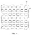
- FIGS. 4 and 5are plan views that illustrate patterns that may be used in accordance with embodiments of the present invention. It should be noted that the patterns are provided for illustrative purposes only, and that the pattern may be of any shape, size, and pattern that is particularly well-suited for a particular application.
- the patterned first mask 106(see FIG. 1 b ) is patterned in a grid shape.
- the LED structurese.g., LED structures 114 and 206 of FIGS. 1 f and 2 c, respectively
- FIG. 5illustrates another embodiment in which the LED structures 114 and 206 are arranged in parallel lines.
- the substratemay be, for example, a p-type substrate (desirable with backside electrical contacts) or an undoped substrate (desirable with a front-side electrical contacts).
- embodiments of the present inventionallow the capability for integrating silicon-based semiconductor devices with LED structures while reducing costs by, for example, using a bulk silicon substrate.
- the use of the silicon substratefurther allows the use of selective epitaxial growth for the LED device and reduces residual stress in the LED device.
- the use of recesses in the substratealso allows the surface area of LED structure to be increased, thereby increasing the emission area and light efficiency.
- Embodiments using a non-conformal or planar contact and active layerssuch as the embodiment discussed above with reference to FIG. 3 , allows a cubic structure of the group III-N layer, which exhibits a higher external quantum efficiency.
Landscapes
- Led Devices (AREA)
- Engineering & Computer Science (AREA)
- Microelectronics & Electronic Packaging (AREA)
Abstract
Description
- This invention relates generally to light-emitting diodes and, more particularly, to light-emitting diodes formed in recesses of a substrate.
- Light emitting diodes (LEDs) are manufactured by forming active regions on a substrate and by depositing various conductive and semiconductive layers on the substrate. The radiative recombination of electron-hole pairs can be used for the generation of electromagnetic radiation (e.g., light) by the electric current in a p-n junction. In a forward-biased p-n junction fabricated from a direct band gap material, such as GaAs or GaN, the recombination of the electron-hole pairs injected into the depletion region causes the emission of electromagnetic radiation. The electromagnetic radiation may be in the visible range or may be in a non-visible range. Different colors of LEDs may be created by using materials with different band gaps. Further, an LED with electromagnetic radiation emitting in a non-visible range may direct the non-visible light towards a phosphor lens or a like material type. When the non-visible light is absorbed by the phosphor, the phosphor emits a visible light.
- LEDs are typically manufactured on a sapphire substrate (Al2O3) for group III-N compound LED structures because the crystal orientation of the sapphire substrate allows the group III-N compounds to be epitaxially grown on the sapphire substrate. Sapphire substrates, however, are expensive as compared to silicon substrates. Also, sapphire substrates are typically characterized by thermal accumulation due to the low thermal conductivity of sapphire.
- Furthermore, LEDs are typically formed on a planar substrate, thereby resulting in a planar LED structure. A planar LED structure limits the amount of light-emitting material that may be placed on a given size of substrate. As a result, the light emitting efficiency of an LED of a given size is restricted.
- Accordingly, there is a need for a structure and a method to form LED devices more cost effectively while increasing the light emitting efficiency of an LED of a given size.
- These and other problems are generally reduced, solved or circumvented, and technical advantages are generally achieved, by embodiments of the present invention, which provides light-emitting diodes (LEDs) formed in recesses of a substrate.
- In an embodiment of the present invention, a method of forming an LED device is provided. The method includes forming recesses in a substrate and forming LED structures within the recesses. The LED structures may have a bottom contact layer that covers the sidewalls of the recesses. The LED structure includes the bottom contact layer, an active layer (e.g., a multiple quantum well), and a top contact layer. Optionally, a buffer layer may be used to facilitate the growth of the bottom contact layer on the substrate. Furthermore, the LED structure may be formed over a top surface of the substrate adjacent to the recesses.
- In another embodiment of the present invention, an LED device is provided. The LED device includes LED structures in recesses of a substrate such that the LED structures cover the sidewalls of the recesses. The LED structure may be formed as conformal layers along sidewalls of the recesses, and optionally over a top surface of the substrate adjacent to the recesses.
- In yet another embodiment of the present invention, another LED device is provided. The LED structure includes a bottom contact layer that has a non-conformal, and preferably a planar, surface as compared to the topology of the recess. The active layer and the top contact layer may be formed as conformal layers over the bottom contact layer.
- For a more complete understanding of the present invention, and the advantages thereof, reference is now made to the following descriptions taken in conjunction with the accompanying drawings, in which:
FIGS. 1 a-1fare cross-section views of a first method of forming LED structures in accordance with an embodiment of the present invention;FIGS. 2 a-2care cross-section views of a second method of forming LED structures in accordance with an embodiment of the present invention;FIG. 3 is a cross-section view of a third method of forming LED structures in accordance with an embodiment of the present invention; andFIGS. 4 and 5 are plan views of examples of patterns that may be used in accordance with embodiments of the present invention.- The making and using of the presently preferred embodiments are discussed in detail below. It should be appreciated, however, that the present invention provides many applicable inventive concepts that can be embodied in a wide variety of specific contexts. The specific embodiments discussed herein are merely illustrative of specific ways to make and use the invention, and do not limit the scope of the invention.
- A novel method for forming light-emitting diodes (LEDs) and the resulting structures are provided. The intermediate stages of manufacturing preferred embodiments of the present invention are illustrated. It should be understood that steps necessary to illustrate the inventive aspects of the invention are shown, but other processes may be performed. Throughout the various views and illustrative embodiments of the present invention, like reference numbers are used to designate like elements.
FIGS. 1 a-1fillustrate cross-section views during various steps of a first method embodiment of the present invention. The process begins inFIG. 1 a,wherein asubstrate 102 having afirst mask 104 formed thereon is shown. Thesubstrate 102 is preferably a bulk semiconductor substrate doped with a dopant of a first conductivity type, preferably having a (100) or (111) surface orientation. Thefirst mask 104 is preferably formed over thesubstrate 102 to protect areas of thesubstrate 102 from a subsequent etching process to form concave structures as discussed below.- It should be noted that while embodiments of the present invention are described in the context of using a bulk silicon substrate, other substrates may be used. For example, silicon-on-insulator (SOI) substrates, sapphire substrates, SiC substrates, and the like may also be used. Embodiments of the present invention, however, may be particularly suited to silicon substrates due to the low cost in addition to reducing the residual stress in the LED structure formed thereon. Silicon substrates may also improve the extraction efficiency and allow a selective group III-N epitaxial growth process to be used.
- The
first mask 104 is preferably a hard mask comprising one or more dielectric layers. In an embodiment, thefirst mask 104 comprises a silicon dioxide layer formed by, for example, thermal oxidation or by chemical vapor deposition (CVD) techniques using tetra-ethyl-ortho-silicate (TEOS) and oxygen as a precursor, or a silicon nitride layer formed using CVD techniques using silane and ammonia as precursor gases. Alternatively, thefirst mask 104 may be formed of other dielectric materials. For example, silicon oxynitride, or the like may also be used. A multi-layer hard mask, such as layers of silicon dioxide and silicon nitride, may also be used. Furthermore, other materials, such as a metal, a metal nitride, a metal oxide, or the like may be used. For example, thefirst mask 104 may be formed of tungsten. - As illustrated in
FIG. 1 b,thefirst mask 104 is subsequently patterned to form a patternedfirst mask 106 in accordance with an embodiment of the present invention. In an embodiment, thefirst mask 104 is patterned using photolithography techniques known in the art. Generally, photolithography techniques involve depositing a photoresist material and irradiating the photoresist material in accordance with a pattern. Thereafter, the photoresist material is developed to remove a portion of the photoresist material. The remaining photoresist material protects the underlying material during subsequent processing steps, such as etching. In this case, the photoresist material is utilized to create a patterned mask to define openings105 (which will become concave recesses in thesubstrate 102 as discussed below). FIG. 1 cillustrates the result of an etching step to formconcave recesses 108 in accordance with an embodiment of the present invention. During this etching process, the patternedfirst mask 106 protects theunderlying substrate 102 from the etch process. As a result, the unprotected portions of thesubstrate 102 are removed, thereby forming theconcave recesses 108. In an embodiment, the etching process is performed at least in part by a wet dip in dilute potassium hydroxide (KOH). Theconcave recesses 108 are preferably about 0.1 μm to about 100 μm wide and about 0.1 μm to about 10 μm deep. Other etching processes, including dry etch processes (e.g., inductively-coupled plasma (ICP) etching, reactive ion etching (RIE), and the like) and/or wet etch processes (e.g., chemical etching, photo-enhance chemical etching, and the like) may be used. It should be noted that theconcave recesses 108 may be of any shape, such as a pyramid, tapered, cylindrical, semisphere, column, rectangular, or the like.- Next, a
separation layer 110 is formed in accordance with an embodiment of the present invention as illustrated inFIG. 1 d.Theseparation layer 110 preferably includes a dielectric material blanket deposited over thesubstrate 102. A metal nitride or other material having a high resistivity, such as AlN that has a resistivity greater than about 1014ohm-cm, may also be used for theseparation layer 110. It should be noted that the materials selected for thefirst mask 104 and theseparation layer 110 are preferably selected such that there is a good etch selectivity between the materials for the different layers for subsequent processing. For example, in an embodiment in which thefirst mask 104 is formed of silicon dioxide, theseparation layer 110 may be a silicon nitride. In this embodiment, theseparation layer 110 may be etched using thermal phosphoric acid at about 120° C., which has a selective etch rate between silicon nitride and silicon dioxide of greater than about100. Theseparation layer 110 is preferably about 5 nm to about 3000 nm in thickness. - The
separation layer 110 is patterned as illustrated inFIG. 1 esuch that theseparation layer 110 is removed except for a portion along the bottom surfaces of theconcave recesses 108, thereby formingseparation regions 112. Theseparation layer 110 may be patterned using photolithography techniques as described above. In this case, a photoresist material may be deposited, exposed, and developed such that the photoresist material remains over theseparation layer 110 along the bottom of theconcave recesses 108. An etch process, such as an anisotropic dry etch process, may be used to remove theunprotected separation layer 110. The remaining portions of theseparation layer 110 form theseparation regions 112 as illustrated inFIG. 1 e. - Thereafter,
LED structures 114 may be formed as illustrated inFIG. 1 fin accordance with an embodiment of the present invention. TheLED structures 114 are formed along the sidewalls of theconcave recesses 108, preferably being separated along the bottom of theconcave recesses 108 by theseparation regions 112. In this manner, theseparation regions 112 act to reduce the residual stress during an epitaxial growth process of theLED structures 114. While theLED structures 114 may extend over theseparation regions 112, it is expected that the residual stress in theLED structures 114 will be diminished. - The
LED structures 114 may comprise any LED structure suitable for a particular application. Generally, theLED structures 114 include afirst contact layer 120 formed over sidewalls of theconcave recesses 108 in thesubstrate 102. Preferably, thefirst contact layer 120 is formed of a group III-N compound doped with a dopant of the first conductivity type (e.g., n-GaN) and may be disposed by, for example, a selective epitaxial growth process such as a molecular-beam epitaxy (MBE), metal organic chemical vapor deposition (MOCVD), Hydride Vapor Phase Epitaxy (HVPE), liquid phase epitaxy (LPE), or the like. The group III-N material may include, for example, GaN, InN, AlN, InxGa(1-x)N, AlxGa(1-x)N, AlxInyGa(1-x-y)N, or the like. Active layer 122 is disposed on thefirst contact layer 120. Theactive layer 122 may comprise multiple quantum wells (MQW) and acts as an active layer for emitting light. MQW structures inactive layer 122, may be layers of InGaN and GaN, for example. MQWs inactive layer 122 may be disposed in an epitaxial reactor.- A
second contact layer 124 is disposed on theactive layer 110. Thesecond contact layer 124 is preferably formed of a group III-N compound doped with a dopant of the second conductivity type (e.g., p-GaN) and may be formed by a process similar to thefirst contact layer 120. - Thereafter, processes may be performed to complete the LED device. For example, electrical contacts (front-side and/or backside contacts) may be formed to the first and second contact layers120 and124, passivation layers may be formed, and the LED device may be diced and packaged.
- It should be noted that the above description describes a method of forming concave recesses in a substrate, in which LED devices may be formed. Other layers, such as a distributed Bragg reflector or a buffer layer, may be desirable. Depending upon the type of substrate and the connections to the first and second contact layers120 and124, a buffer layer may also be desirable between the
first contact layer 120 and thesubstrate 102. For example, with some types of substrates, such as SiC substrates, a buffer layer, such as AlN or AlGaN, may be desirable to aid in the selective epitaxial growth of a group III-N compound on the SiC substrate. A distributed Bragg reflector generally comprises multiple layers having different refractive indices that cause light emitted from the LED structures to be reflected, thereby increasing the light emitted from the top of the LED device. A reflective buffer layer may also be used with or in place of the distributed Bragg reflector. - The structure of the
LED structures 114 may also vary depending on the type of materials used and the intended application. It is expected that many types of LED structures may be used with embodiments of the present invention, which provides concave recesses in a substrate in which LED structures may be formed. - Advantageously, one of ordinary skill in the art will realize that due to the non-planar surface of the
LED structures 114, the total area ofactive layer 122 is advantageously increased as compared to a planar MQW occupying the same chip area. As a result, the light emitting efficiency is increased. - It should also be noted that the above description assumes a backside contact for the
first contact layer 120, which typically uses adoped substrate 102. In situations in which a front-side contact is utilized to provide an electrical contact to thefirst contact layer 120, anundoped substrate 102 may be used. FIGS. 2 a-2cillustrate cross-section views during various steps of a second method embodiment of the present invention. The process illustrated inFIGS. 2 a-2cassumes processes, materials, and structures similar to those discussed above with reference toFIGS. 1 a-1c,wherein like reference numerals refer to like elements.- Referring now to
FIG. 2 a,which illustrates an intermediate process step subsequent toFIG. 1 c,the patterned first mask106 (seeFIG. 1 c) is removed and aseparation layer 202 is formed in accordance with an embodiment of the present invention. The patternedfirst mask 106 may be removed, for example, by a wet dip in a dilute hydrofluoric acid. - Thereafter, the
separation layer 202 is formed as a conformal layer over the surface of thesubstrate 102. Theseparation layer 202 is preferably a dielectric layer, such as silicon dioxide that may be formed in a manner similar to theseparation layer 110 discussed above with reference toFIG. 1 d. FIG. 2 billustrates the patterning of theseparation layer 202 to form theseparation regions 204. Theseparation layer 202 is patterned to formseparation regions 204 along the bottom of theconcave recesses 108. Theseparation regions 204 may be formed using photolithography techniques and an etch process, such as an anisotropic dry etch process, as discussed above with reference toFIG. 1 e.- Thereafter, as illustrated in
FIG. 2 c,theLED structures 206 may be formed in the same manner as theLED structures 114, except that theLED structures 206 overlay a top surface of thesubstrate 102 between adjacentconcave recesses 108. Because the patterned first mask106 (seeFIG. 1 c) has been removed, thereby exposing the underlying substrate, theLED structures 206, which are formed by selective epitaxial growth, will be formed on the top exposed surface of thesubstrate 102 between theconcave recesses 108 as well as on the exposed sidewalls of theconcave recesses 108. In this manner, an even greater amount of surface area of theLED structures 206 is created. As a result the light emitted efficiency is increased as compared to a planar surface or the embodiment described above with reference toFIG. 1 f. FIG. 3 illustrates cross-section views during various steps of a third method embodiment of the present invention. The process illustrated inFIG. 3 assumes processes, materials, and structures similar to those discussed above with reference toFIGS. 1 a-1e,wherein like reference numerals refer to like elements.- Referring now to
FIG. 3 , which illustrates a process step subsequent toFIG. 1 e,aplanar LED structure 310 is formed within theconcave recesses 108, substantially filling the recesses. In this embodiment, theLED structure 310 is preferably formed using processes that result in afirst contact layer 312 having a non-conformal surface relative to theunderlying substrate 102. In a preferred embodiment, the top surface of the first contact layer is planar, and even more preferably, the top surface of the first contact layer is co-planar with the top surface of thesubstrate 102. For example, in an embodiment in which an n-GaN/MQW/p-GaN LED structure is utilized, the n-GaN layer for thefirst contact layer 312 may be formed by, for example, a metal organic vapor phase epitaxy process by placing the substrate in reaction chamber of a MOVPD apparatus heated to about 1,000° C., wherein hydrogen, ammonia, and trimethyl gallium (TMGa) are supplied in the reaction chamber. In order to form n-type doped GaN, silane (SiH4) is also introduced into the reaction chamber. A pressure in the reaction chamber of about 40 torr may be used. Anactive layer 314 and a second contact layer316 (e.g., a p-GaN layer) may be formed using processes similar to those discussed above with reference to theactive layer 122 and thesecond contact layer 124, respectively, wherein bis-cyclopentadienylmagnesium (CP2Mg) is provided in the reaction chamber instead of silane to form p-GaN. - In this embodiment, it should be noted that the patterned
first mask 106 may optionally be removed. Furthermore, if the patterned first mask remains and comprises a metal or other conductive material, then it is preferred that thefirst contact layer 312 extend above the patternedfirst mask 106 to prevent a short condition between thefirst contact layer 312 and thesecond contact layer 316. - One of ordinary skill in the art will appreciate that while this embodiment has a first contact layer and an active layer with less surface area than the embodiments discussed above with reference to
FIGS. 1 a-1fand2a-2c,the use of a recessed substrate may result in an epitaxial GaN layer having a cubic structure with a non-polar characteristic. This arrangement may allow a higher external quantum efficiency than may be achieved with a planar layer of GaN formed along a surface of a substrate. - It should also be noted that because the
separation regions 112 are completely covered with thefirst contact layer 312 in this embodiment, theseparation regions 112 may be formed with a dielectric material, metal, or a metal nitride. FIGS. 4 and 5 are plan views that illustrate patterns that may be used in accordance with embodiments of the present invention. It should be noted that the patterns are provided for illustrative purposes only, and that the pattern may be of any shape, size, and pattern that is particularly well-suited for a particular application. Referring first toFIG. 4 , the patterned first mask106 (seeFIG. 1 b) is patterned in a grid shape. As a result, the LED structures (e.g.,LED structures FIGS. 1 fand2c,respectively) will be formed in a matrix or grid of recesses.FIG. 5 illustrates another embodiment in which theLED structures - In the foregoing specification, the invention has been described with reference to specific embodiments. However, various modifications and changes can be made by one skilled in the art without departing from the scope of the present invention. Accordingly, the specification and figures are to be regarded in an illustrative rather than a restrictive sense, and all such modifications are intended to be included within the scope of the present invention.
- For example, while the present invention has been illustrated with reference to an n-type substrate and an LED structure having top-to-bottom layers comprising n-GaN, active layer, and p-GaN, an LED structure having top-to-bottom layers comprising p-GaN, active layer, and n-GaN may be used. Additionally, other types of materials besides GaN may be used. In this embodiment, the substrate may be, for example, a p-type substrate (desirable with backside electrical contacts) or an undoped substrate (desirable with a front-side electrical contacts).
- One of ordinary skill in the art will appreciate that embodiments of the present invention allow the capability for integrating silicon-based semiconductor devices with LED structures while reducing costs by, for example, using a bulk silicon substrate. The use of the silicon substrate further allows the use of selective epitaxial growth for the LED device and reduces residual stress in the LED device. The use of recesses in the substrate also allows the surface area of LED structure to be increased, thereby increasing the emission area and light efficiency. Embodiments using a non-conformal or planar contact and active layers, such as the embodiment discussed above with reference to
FIG. 3 , allows a cubic structure of the group III-N layer, which exhibits a higher external quantum efficiency. - Although particular embodiments of the invention have been described in detail, it is understood that the invention is not limited correspondingly in scope, but includes all changes, modifications, and equivalents coming within the spirit and terms of the claims appended hereto. For example, differing types of materials and differing thicknesses may be used, and the like. Accordingly, it is understood that this invention may be extended to other structures and materials, and thus, the specification and figures are to be regarded in an illustrative rather than a restrictive sense.
Claims (20)
Priority Applications (5)
| Application Number | Priority Date | Filing Date | Title |
|---|---|---|---|
| US12/247,895US8134163B2 (en) | 2008-08-11 | 2008-10-08 | Light-emitting diodes on concave texture substrate |
| TW098115303ATWI484657B (en) | 2008-08-11 | 2009-05-08 | Light-emitting diode |
| CN2009101389552ACN101651181B (en) | 2008-08-11 | 2009-05-21 | led |
| US13/358,327US8629465B2 (en) | 2008-08-11 | 2012-01-25 | Light-emitting diodes on concave texture substrate |
| US14/091,843US9373755B2 (en) | 2008-08-11 | 2013-11-27 | Light-emitting diodes on concave texture substrate |
Applications Claiming Priority (2)
| Application Number | Priority Date | Filing Date | Title |
|---|---|---|---|
| US8789708P | 2008-08-11 | 2008-08-11 | |
| US12/247,895US8134163B2 (en) | 2008-08-11 | 2008-10-08 | Light-emitting diodes on concave texture substrate |
Related Child Applications (1)
| Application Number | Title | Priority Date | Filing Date |
|---|---|---|---|
| US13/358,327DivisionUS8629465B2 (en) | 2008-08-11 | 2012-01-25 | Light-emitting diodes on concave texture substrate |
Publications (2)
| Publication Number | Publication Date |
|---|---|
| US20100032700A1true US20100032700A1 (en) | 2010-02-11 |
| US8134163B2 US8134163B2 (en) | 2012-03-13 |
Family
ID=41652064
Family Applications (3)
| Application Number | Title | Priority Date | Filing Date |
|---|---|---|---|
| US12/247,895Active2029-06-09US8134163B2 (en) | 2008-08-11 | 2008-10-08 | Light-emitting diodes on concave texture substrate |
| US13/358,327ActiveUS8629465B2 (en) | 2008-08-11 | 2012-01-25 | Light-emitting diodes on concave texture substrate |
| US14/091,843Active2028-10-24US9373755B2 (en) | 2008-08-11 | 2013-11-27 | Light-emitting diodes on concave texture substrate |
Family Applications After (2)
| Application Number | Title | Priority Date | Filing Date |
|---|---|---|---|
| US13/358,327ActiveUS8629465B2 (en) | 2008-08-11 | 2012-01-25 | Light-emitting diodes on concave texture substrate |
| US14/091,843Active2028-10-24US9373755B2 (en) | 2008-08-11 | 2013-11-27 | Light-emitting diodes on concave texture substrate |
Country Status (3)
| Country | Link |
|---|---|
| US (3) | US8134163B2 (en) |
| CN (1) | CN101651181B (en) |
| TW (1) | TWI484657B (en) |
Cited By (4)
| Publication number | Priority date | Publication date | Assignee | Title |
|---|---|---|---|---|
| US20110220930A1 (en)* | 2010-03-09 | 2011-09-15 | Taiwan Semiconductor Manufacturing Company, Ltd. | Light-Emitting Devices with Textured Active Layer |
| GB2527045A (en)* | 2014-06-09 | 2015-12-16 | Seren Photonics Ltd | Fabrication of semi-polar crystal structures |
| US20220209061A1 (en)* | 2020-12-30 | 2022-06-30 | Applied Materials, Inc. | Methods for forming light emitting diodes |
| US11715753B2 (en)* | 2020-12-30 | 2023-08-01 | Applied Materials, Inc. | Methods for integration of light emitting diodes and image sensors |
Families Citing this family (22)
| Publication number | Priority date | Publication date | Assignee | Title |
|---|---|---|---|---|
| US8134163B2 (en) | 2008-08-11 | 2012-03-13 | Taiwan Semiconductor Manfacturing Co., Ltd. | Light-emitting diodes on concave texture substrate |
| US8859305B2 (en)* | 2010-02-10 | 2014-10-14 | Macron Technology, Inc. | Light emitting diodes and associated methods of manufacturing |
| US8390010B2 (en) | 2010-03-25 | 2013-03-05 | Micron Technology, Inc. | Solid state lighting devices with cellular arrays and associated methods of manufacturing |
| CN102347416A (en)* | 2010-08-02 | 2012-02-08 | 亚威朗光电(中国)有限公司 | Light emitting diode |
| TWI456753B (en)* | 2010-12-09 | 2014-10-11 | Ind Tech Res Inst | Nitride semiconductor template and fabricating method thereof |
| US8803185B2 (en)* | 2012-02-21 | 2014-08-12 | Peiching Ling | Light emitting diode package and method of fabricating the same |
| TWI469389B (en)* | 2012-06-19 | 2015-01-11 | Lextar Electronics Corp | Vertical solid state light emitting device process |
| EP2943985B1 (en)* | 2013-01-08 | 2021-07-07 | Lumileds LLC | Shaped led for enhanced light extraction efficiency |
| US9970126B2 (en) | 2013-02-26 | 2018-05-15 | Massachusetts Institute Of Technology | Production of free-standing crystalline material layers |
| US9892944B2 (en) | 2016-06-23 | 2018-02-13 | Sharp Kabushiki Kaisha | Diodes offering asymmetric stability during fluidic assembly |
| US9917226B1 (en) | 2016-09-15 | 2018-03-13 | Sharp Kabushiki Kaisha | Substrate features for enhanced fluidic assembly of electronic devices |
| US10249599B2 (en) | 2016-06-29 | 2019-04-02 | eLux, Inc. | Laminated printed color conversion phosphor sheets |
| US9985190B2 (en) | 2016-05-18 | 2018-05-29 | eLux Inc. | Formation and structure of post enhanced diodes for orientation control |
| US9755110B1 (en) | 2016-07-27 | 2017-09-05 | Sharp Laboratories Of America, Inc. | Substrate with topological features for steering fluidic assembly LED disks |
| US9722145B2 (en) | 2015-06-24 | 2017-08-01 | Sharp Laboratories Of America, Inc. | Light emitting device and fluidic manufacture thereof |
| US9627437B1 (en) | 2016-06-30 | 2017-04-18 | Sharp Laboratories Of America, Inc. | Patterned phosphors in through hole via (THV) glass |
| US10243097B2 (en) | 2016-09-09 | 2019-03-26 | eLux Inc. | Fluidic assembly using tunable suspension flow |
| US9837390B1 (en) | 2016-11-07 | 2017-12-05 | Corning Incorporated | Systems and methods for creating fluidic assembly structures on a substrate |
| US10062674B1 (en)* | 2017-04-28 | 2018-08-28 | Corning Incorporated | Systems and methods for display formation using photo-machinable material substrate layers |
| US10389090B2 (en)* | 2017-11-21 | 2019-08-20 | International Business Machines Corporation | Lateral growth of edge-emitting lasers |
| US20240006552A1 (en)* | 2020-11-18 | 2024-01-04 | Enkris Semiconductor, Inc. | Light-emitting device and manufacturing method therefor |
| KR102863094B1 (en) | 2020-12-02 | 2025-09-25 | 삼성디스플레이 주식회사 | Display device and manufacturing method for light emitting element |
Citations (8)
| Publication number | Priority date | Publication date | Assignee | Title |
|---|---|---|---|---|
| US5930279A (en)* | 1996-04-23 | 1999-07-27 | Compagnie Industrielle Des Lasers Cilas | Diode laser device arranged in the form of semiconductor arrays |
| US6531328B1 (en)* | 2001-10-11 | 2003-03-11 | Solidlite Corporation | Packaging of light-emitting diode |
| US6635901B2 (en)* | 2000-12-15 | 2003-10-21 | Nobuhiko Sawaki | Semiconductor device including an InGaAIN layer |
| US6844572B2 (en)* | 2002-03-19 | 2005-01-18 | Sharp Kabushiki Kaisha | Light emitting semiconductor device and method of fabricating the same |
| US20050145862A1 (en)* | 2003-12-31 | 2005-07-07 | Lg Electronics Inc. | Light emitting device and manufacturing method thereof |
| US20070145382A1 (en)* | 2005-12-28 | 2007-06-28 | Samsung Electro-Mechanics Co., Ltd. | Semiconductor light emitting diode and method for manufacturing the same |
| US20080308835A1 (en)* | 2007-06-12 | 2008-12-18 | Pan Shaoher X | Silicon based solid state lighting |
| US20090032799A1 (en)* | 2007-06-12 | 2009-02-05 | Siphoton, Inc | Light emitting device |
Family Cites Families (7)
| Publication number | Priority date | Publication date | Assignee | Title |
|---|---|---|---|---|
| JPH10223368A (en)* | 1997-01-31 | 1998-08-21 | Hokuriku Electric Ind Co Ltd | Organic el element and its manufacture |
| KR100277940B1 (en)* | 1998-07-14 | 2001-02-01 | 구자홍 | GAN semiconductor laser diode and manufacturing method thereof |
| JP3416083B2 (en)* | 1999-08-31 | 2003-06-16 | 株式会社日立製作所 | Semiconductor device |
| JP4651161B2 (en)* | 2000-07-03 | 2011-03-16 | 宣彦 澤木 | Semiconductor device and manufacturing method thereof |
| US20020153529A1 (en)* | 2001-04-24 | 2002-10-24 | Jin-Shown Shie | LED array with optical isolation structure and method of manufacturing the same |
| MY151572A (en)* | 2005-06-02 | 2014-06-13 | Univ Illinois | Printable semiconductor structures and related methods of making and assembling |
| US8134163B2 (en) | 2008-08-11 | 2012-03-13 | Taiwan Semiconductor Manfacturing Co., Ltd. | Light-emitting diodes on concave texture substrate |
- 2008
- 2008-10-08USUS12/247,895patent/US8134163B2/enactiveActive
- 2009
- 2009-05-08TWTW098115303Apatent/TWI484657B/enactive
- 2009-05-21CNCN2009101389552Apatent/CN101651181B/enactiveActive
- 2012
- 2012-01-25USUS13/358,327patent/US8629465B2/enactiveActive
- 2013
- 2013-11-27USUS14/091,843patent/US9373755B2/enactiveActive
Patent Citations (8)
| Publication number | Priority date | Publication date | Assignee | Title |
|---|---|---|---|---|
| US5930279A (en)* | 1996-04-23 | 1999-07-27 | Compagnie Industrielle Des Lasers Cilas | Diode laser device arranged in the form of semiconductor arrays |
| US6635901B2 (en)* | 2000-12-15 | 2003-10-21 | Nobuhiko Sawaki | Semiconductor device including an InGaAIN layer |
| US6531328B1 (en)* | 2001-10-11 | 2003-03-11 | Solidlite Corporation | Packaging of light-emitting diode |
| US6844572B2 (en)* | 2002-03-19 | 2005-01-18 | Sharp Kabushiki Kaisha | Light emitting semiconductor device and method of fabricating the same |
| US20050145862A1 (en)* | 2003-12-31 | 2005-07-07 | Lg Electronics Inc. | Light emitting device and manufacturing method thereof |
| US20070145382A1 (en)* | 2005-12-28 | 2007-06-28 | Samsung Electro-Mechanics Co., Ltd. | Semiconductor light emitting diode and method for manufacturing the same |
| US20080308835A1 (en)* | 2007-06-12 | 2008-12-18 | Pan Shaoher X | Silicon based solid state lighting |
| US20090032799A1 (en)* | 2007-06-12 | 2009-02-05 | Siphoton, Inc | Light emitting device |
Cited By (12)
| Publication number | Priority date | Publication date | Assignee | Title |
|---|---|---|---|---|
| US20110220930A1 (en)* | 2010-03-09 | 2011-09-15 | Taiwan Semiconductor Manufacturing Company, Ltd. | Light-Emitting Devices with Textured Active Layer |
| US8299479B2 (en)* | 2010-03-09 | 2012-10-30 | Tsmc Solid State Lighting Ltd. | Light-emitting devices with textured active layer |
| US20130045556A1 (en)* | 2010-03-09 | 2013-02-21 | Tsmc Solid State Lighting Ltd. | Light-Emitting Devices with Textured Active Layer |
| US8673666B2 (en)* | 2010-03-09 | 2014-03-18 | Tsmc Solid State Lighting Ltd. | Light-emitting devices with textured active layer |
| GB2527045A (en)* | 2014-06-09 | 2015-12-16 | Seren Photonics Ltd | Fabrication of semi-polar crystal structures |
| WO2015189582A1 (en)* | 2014-06-09 | 2015-12-17 | Seren Photonics Limited | Fabrication of semi-polar crystal structures |
| JP2017523599A (en)* | 2014-06-09 | 2017-08-17 | セレン フォトニクス リミテッド | Production of semipolar crystal structure |
| GB2527045B (en)* | 2014-06-09 | 2018-12-19 | Seren Photonics Ltd | Fabrication of semi-polar crystal structures |
| US10290497B2 (en) | 2014-06-09 | 2019-05-14 | Seren Photonics Limited | Fabrication of semi-polar crystal structures |
| US20220209061A1 (en)* | 2020-12-30 | 2022-06-30 | Applied Materials, Inc. | Methods for forming light emitting diodes |
| US11715753B2 (en)* | 2020-12-30 | 2023-08-01 | Applied Materials, Inc. | Methods for integration of light emitting diodes and image sensors |
| US11811000B2 (en)* | 2020-12-30 | 2023-11-07 | Applied Materials, Inc. | Methods for forming light emitting diodes |
Also Published As
| Publication number | Publication date |
|---|---|
| TW201007987A (en) | 2010-02-16 |
| US20120119236A1 (en) | 2012-05-17 |
| TWI484657B (en) | 2015-05-11 |
| CN101651181A (en) | 2010-02-17 |
| US8629465B2 (en) | 2014-01-14 |
| US8134163B2 (en) | 2012-03-13 |
| CN101651181B (en) | 2011-06-15 |
| US9373755B2 (en) | 2016-06-21 |
| US20140087505A1 (en) | 2014-03-27 |
Similar Documents
| Publication | Publication Date | Title |
|---|---|---|
| US8134163B2 (en) | Light-emitting diodes on concave texture substrate | |
| US10062821B2 (en) | Light-emitting device | |
| US8659033B2 (en) | Light-emitting diode with textured substrate | |
| US9117943B2 (en) | Semiconductor package with through silicon vias | |
| US8742441B2 (en) | Light-emitting diode with embedded elements | |
| US8486730B2 (en) | Method of separating light-emitting diode from a growth substrate | |
| KR102496367B1 (en) | Optoelectronic devices with light emitting diodes | |
| KR20110030542A (en) | Optoelectronic device manufacturing method and photoelectric device | |
| KR101351484B1 (en) | Light emitting device having nitride-based semiconductor omnidirectional reflector | |
| KR20250050979A (en) | LED Arrays | |
| KR20130006976A (en) | Light emitting device, method for fabricating the same and substrate for light emitting device | |
| US20100051965A1 (en) | Carbon-Containing Semiconductor Substrate | |
| KR102249624B1 (en) | Light emitting structure and Light emitting device having the same | |
| KR20120005662A (en) | Light emitting element | |
| KR101701041B1 (en) | Light emitting diode formed on silicon polyhedron and method for fabricating the same | |
| WO2025149575A1 (en) | Light emitting device with at least one sacrificial quantum well | |
| TWI424589B (en) | Light-emitting diode device and method of forming same | |
| KR101650722B1 (en) | Nitride semiconductor light emitting device | |
| KR20130006972A (en) | The light emitting device and the mathod for manufacturing the same | |
| KR20130006977A (en) | Light emitting device and method for fabricating the same |
Legal Events
| Date | Code | Title | Description |
|---|---|---|---|
| AS | Assignment | Owner name:TAIWAN SEMICONDUCTOR MANUFACTURING COMPANY, LTD.,T Free format text:ASSIGNMENT OF ASSIGNORS INTEREST;ASSIGNORS:YU, CHEN-HUA;LIN, HUNG-TA;CHIOU, WEN-CHIH;AND OTHERS;REEL/FRAME:021766/0509 Effective date:20080818 Owner name:TAIWAN SEMICONDUCTOR MANUFACTURING COMPANY, LTD., Free format text:ASSIGNMENT OF ASSIGNORS INTEREST;ASSIGNORS:YU, CHEN-HUA;LIN, HUNG-TA;CHIOU, WEN-CHIH;AND OTHERS;REEL/FRAME:021766/0509 Effective date:20080818 | |
| STCF | Information on status: patent grant | Free format text:PATENTED CASE | |
| FPAY | Fee payment | Year of fee payment:4 | |
| AS | Assignment | Owner name:CHIP STAR LTD., TAIWAN Free format text:ASSIGNMENT OF ASSIGNORS INTEREST;ASSIGNOR:TAIWAN SEMICONDUCTOR MANUFACTURING COMPANY, LTD.;REEL/FRAME:038460/0374 Effective date:20150624 | |
| AS | Assignment | Owner name:EPISTAR CORPORATION, TAIWAN Free format text:MERGER;ASSIGNOR:CHIP STAR LTD.;REEL/FRAME:038475/0854 Effective date:20150715 | |
| MAFP | Maintenance fee payment | Free format text:PAYMENT OF MAINTENANCE FEE, 8TH YEAR, LARGE ENTITY (ORIGINAL EVENT CODE: M1552); ENTITY STATUS OF PATENT OWNER: LARGE ENTITY Year of fee payment:8 | |
| MAFP | Maintenance fee payment | Free format text:PAYMENT OF MAINTENANCE FEE, 12TH YEAR, LARGE ENTITY (ORIGINAL EVENT CODE: M1553); ENTITY STATUS OF PATENT OWNER: LARGE ENTITY Year of fee payment:12 |