US20100019359A1 - Semiconductor Device and Method of Forming Shielding Along a Profile Disposed in Peripheral Region Around the Device - Google Patents
Semiconductor Device and Method of Forming Shielding Along a Profile Disposed in Peripheral Region Around the DeviceDownload PDFInfo
- Publication number
- US20100019359A1 US20100019359A1US12/572,568US57256809AUS2010019359A1US 20100019359 A1US20100019359 A1US 20100019359A1US 57256809 AUS57256809 AUS 57256809AUS 2010019359 A1US2010019359 A1US 2010019359A1
- Authority
- US
- United States
- Prior art keywords
- semiconductor die
- shielding layer
- conductive
- layer
- semiconductor
- Prior art date
- Legal status (The legal status is an assumption and is not a legal conclusion. Google has not performed a legal analysis and makes no representation as to the accuracy of the status listed.)
- Granted
Links
Images


Classifications
- H—ELECTRICITY
- H01—ELECTRIC ELEMENTS
- H01L—SEMICONDUCTOR DEVICES NOT COVERED BY CLASS H10
- H01L25/00—Assemblies consisting of a plurality of semiconductor or other solid state devices
- H01L25/03—Assemblies consisting of a plurality of semiconductor or other solid state devices all the devices being of a type provided for in a single subclass of subclasses H10B, H10D, H10F, H10H, H10K or H10N, e.g. assemblies of rectifier diodes
- H01L25/10—Assemblies consisting of a plurality of semiconductor or other solid state devices all the devices being of a type provided for in a single subclass of subclasses H10B, H10D, H10F, H10H, H10K or H10N, e.g. assemblies of rectifier diodes the devices having separate containers
- H01L25/105—Assemblies consisting of a plurality of semiconductor or other solid state devices all the devices being of a type provided for in a single subclass of subclasses H10B, H10D, H10F, H10H, H10K or H10N, e.g. assemblies of rectifier diodes the devices having separate containers the devices being integrated devices of class H10
- H—ELECTRICITY
- H01—ELECTRIC ELEMENTS
- H01L—SEMICONDUCTOR DEVICES NOT COVERED BY CLASS H10
- H01L21/00—Processes or apparatus adapted for the manufacture or treatment of semiconductor or solid state devices or of parts thereof
- H01L21/02—Manufacture or treatment of semiconductor devices or of parts thereof
- H01L21/04—Manufacture or treatment of semiconductor devices or of parts thereof the devices having potential barriers, e.g. a PN junction, depletion layer or carrier concentration layer
- H01L21/50—Assembly of semiconductor devices using processes or apparatus not provided for in a single one of the groups H01L21/18 - H01L21/326 or H10D48/04 - H10D48/07 e.g. sealing of a cap to a base of a container
- H01L21/56—Encapsulations, e.g. encapsulation layers, coatings
- H01L21/568—Temporary substrate used as encapsulation process aid
- H—ELECTRICITY
- H01—ELECTRIC ELEMENTS
- H01L—SEMICONDUCTOR DEVICES NOT COVERED BY CLASS H10
- H01L21/00—Processes or apparatus adapted for the manufacture or treatment of semiconductor or solid state devices or of parts thereof
- H01L21/67—Apparatus specially adapted for handling semiconductor or electric solid state devices during manufacture or treatment thereof; Apparatus specially adapted for handling wafers during manufacture or treatment of semiconductor or electric solid state devices or components ; Apparatus not specifically provided for elsewhere
- H01L21/683—Apparatus specially adapted for handling semiconductor or electric solid state devices during manufacture or treatment thereof; Apparatus specially adapted for handling wafers during manufacture or treatment of semiconductor or electric solid state devices or components ; Apparatus not specifically provided for elsewhere for supporting or gripping
- H01L21/6835—Apparatus specially adapted for handling semiconductor or electric solid state devices during manufacture or treatment thereof; Apparatus specially adapted for handling wafers during manufacture or treatment of semiconductor or electric solid state devices or components ; Apparatus not specifically provided for elsewhere for supporting or gripping using temporarily an auxiliary support
- H—ELECTRICITY
- H01—ELECTRIC ELEMENTS
- H01L—SEMICONDUCTOR DEVICES NOT COVERED BY CLASS H10
- H01L23/00—Details of semiconductor or other solid state devices
- H01L23/28—Encapsulations, e.g. encapsulating layers, coatings, e.g. for protection
- H01L23/29—Encapsulations, e.g. encapsulating layers, coatings, e.g. for protection characterised by the material, e.g. carbon
- H—ELECTRICITY
- H01—ELECTRIC ELEMENTS
- H01L—SEMICONDUCTOR DEVICES NOT COVERED BY CLASS H10
- H01L23/00—Details of semiconductor or other solid state devices
- H01L23/28—Encapsulations, e.g. encapsulating layers, coatings, e.g. for protection
- H01L23/31—Encapsulations, e.g. encapsulating layers, coatings, e.g. for protection characterised by the arrangement or shape
- H01L23/3107—Encapsulations, e.g. encapsulating layers, coatings, e.g. for protection characterised by the arrangement or shape the device being completely enclosed
- H01L23/3114—Encapsulations, e.g. encapsulating layers, coatings, e.g. for protection characterised by the arrangement or shape the device being completely enclosed the device being a chip scale package, e.g. CSP
- H—ELECTRICITY
- H01—ELECTRIC ELEMENTS
- H01L—SEMICONDUCTOR DEVICES NOT COVERED BY CLASS H10
- H01L23/00—Details of semiconductor or other solid state devices
- H01L23/552—Protection against radiation, e.g. light or electromagnetic waves
- H—ELECTRICITY
- H01—ELECTRIC ELEMENTS
- H01L—SEMICONDUCTOR DEVICES NOT COVERED BY CLASS H10
- H01L24/00—Arrangements for connecting or disconnecting semiconductor or solid-state bodies; Methods or apparatus related thereto
- H01L24/01—Means for bonding being attached to, or being formed on, the surface to be connected, e.g. chip-to-package, die-attach, "first-level" interconnects; Manufacturing methods related thereto
- H01L24/18—High density interconnect [HDI] connectors; Manufacturing methods related thereto
- H01L24/19—Manufacturing methods of high density interconnect preforms
- H—ELECTRICITY
- H01—ELECTRIC ELEMENTS
- H01L—SEMICONDUCTOR DEVICES NOT COVERED BY CLASS H10
- H01L24/00—Arrangements for connecting or disconnecting semiconductor or solid-state bodies; Methods or apparatus related thereto
- H01L24/01—Means for bonding being attached to, or being formed on, the surface to be connected, e.g. chip-to-package, die-attach, "first-level" interconnects; Manufacturing methods related thereto
- H01L24/18—High density interconnect [HDI] connectors; Manufacturing methods related thereto
- H01L24/20—Structure, shape, material or disposition of high density interconnect preforms
- H—ELECTRICITY
- H01—ELECTRIC ELEMENTS
- H01L—SEMICONDUCTOR DEVICES NOT COVERED BY CLASS H10
- H01L24/00—Arrangements for connecting or disconnecting semiconductor or solid-state bodies; Methods or apparatus related thereto
- H01L24/80—Methods for connecting semiconductor or other solid state bodies using means for bonding being attached to, or being formed on, the surface to be connected
- H01L24/82—Methods for connecting semiconductor or other solid state bodies using means for bonding being attached to, or being formed on, the surface to be connected by forming build-up interconnects at chip-level, e.g. for high density interconnects [HDI]
- H—ELECTRICITY
- H01—ELECTRIC ELEMENTS
- H01L—SEMICONDUCTOR DEVICES NOT COVERED BY CLASS H10
- H01L24/00—Arrangements for connecting or disconnecting semiconductor or solid-state bodies; Methods or apparatus related thereto
- H01L24/93—Batch processes
- H01L24/95—Batch processes at chip-level, i.e. with connecting carried out on a plurality of singulated devices, i.e. on diced chips
- H01L24/96—Batch processes at chip-level, i.e. with connecting carried out on a plurality of singulated devices, i.e. on diced chips the devices being encapsulated in a common layer, e.g. neo-wafer or pseudo-wafer, said common layer being separable into individual assemblies after connecting
- H—ELECTRICITY
- H01—ELECTRIC ELEMENTS
- H01L—SEMICONDUCTOR DEVICES NOT COVERED BY CLASS H10
- H01L2221/00—Processes or apparatus adapted for the manufacture or treatment of semiconductor or solid state devices or of parts thereof covered by H01L21/00
- H01L2221/67—Apparatus for handling semiconductor or electric solid state devices during manufacture or treatment thereof; Apparatus for handling wafers during manufacture or treatment of semiconductor or electric solid state devices or components; Apparatus not specifically provided for elsewhere
- H01L2221/683—Apparatus for handling semiconductor or electric solid state devices during manufacture or treatment thereof; Apparatus for handling wafers during manufacture or treatment of semiconductor or electric solid state devices or components; Apparatus not specifically provided for elsewhere for supporting or gripping
- H01L2221/68304—Apparatus for handling semiconductor or electric solid state devices during manufacture or treatment thereof; Apparatus for handling wafers during manufacture or treatment of semiconductor or electric solid state devices or components; Apparatus not specifically provided for elsewhere for supporting or gripping using temporarily an auxiliary support
- H01L2221/68345—Apparatus for handling semiconductor or electric solid state devices during manufacture or treatment thereof; Apparatus for handling wafers during manufacture or treatment of semiconductor or electric solid state devices or components; Apparatus not specifically provided for elsewhere for supporting or gripping using temporarily an auxiliary support used as a support during the manufacture of self supporting substrates
- H—ELECTRICITY
- H01—ELECTRIC ELEMENTS
- H01L—SEMICONDUCTOR DEVICES NOT COVERED BY CLASS H10
- H01L2224/00—Indexing scheme for arrangements for connecting or disconnecting semiconductor or solid-state bodies and methods related thereto as covered by H01L24/00
- H01L2224/01—Means for bonding being attached to, or being formed on, the surface to be connected, e.g. chip-to-package, die-attach, "first-level" interconnects; Manufacturing methods related thereto
- H01L2224/02—Bonding areas; Manufacturing methods related thereto
- H01L2224/04—Structure, shape, material or disposition of the bonding areas prior to the connecting process
- H01L2224/0401—Bonding areas specifically adapted for bump connectors, e.g. under bump metallisation [UBM]
- H—ELECTRICITY
- H01—ELECTRIC ELEMENTS
- H01L—SEMICONDUCTOR DEVICES NOT COVERED BY CLASS H10
- H01L2224/00—Indexing scheme for arrangements for connecting or disconnecting semiconductor or solid-state bodies and methods related thereto as covered by H01L24/00
- H01L2224/01—Means for bonding being attached to, or being formed on, the surface to be connected, e.g. chip-to-package, die-attach, "first-level" interconnects; Manufacturing methods related thereto
- H01L2224/02—Bonding areas; Manufacturing methods related thereto
- H01L2224/04—Structure, shape, material or disposition of the bonding areas prior to the connecting process
- H01L2224/04042—Bonding areas specifically adapted for wire connectors, e.g. wirebond pads
- H—ELECTRICITY
- H01—ELECTRIC ELEMENTS
- H01L—SEMICONDUCTOR DEVICES NOT COVERED BY CLASS H10
- H01L2224/00—Indexing scheme for arrangements for connecting or disconnecting semiconductor or solid-state bodies and methods related thereto as covered by H01L24/00
- H01L2224/01—Means for bonding being attached to, or being formed on, the surface to be connected, e.g. chip-to-package, die-attach, "first-level" interconnects; Manufacturing methods related thereto
- H01L2224/02—Bonding areas; Manufacturing methods related thereto
- H01L2224/04—Structure, shape, material or disposition of the bonding areas prior to the connecting process
- H01L2224/04105—Bonding areas formed on an encapsulation of the semiconductor or solid-state body, e.g. bonding areas on chip-scale packages
- H—ELECTRICITY
- H01—ELECTRIC ELEMENTS
- H01L—SEMICONDUCTOR DEVICES NOT COVERED BY CLASS H10
- H01L2224/00—Indexing scheme for arrangements for connecting or disconnecting semiconductor or solid-state bodies and methods related thereto as covered by H01L24/00
- H01L2224/01—Means for bonding being attached to, or being formed on, the surface to be connected, e.g. chip-to-package, die-attach, "first-level" interconnects; Manufacturing methods related thereto
- H01L2224/02—Bonding areas; Manufacturing methods related thereto
- H01L2224/04—Structure, shape, material or disposition of the bonding areas prior to the connecting process
- H01L2224/05—Structure, shape, material or disposition of the bonding areas prior to the connecting process of an individual bonding area
- H01L2224/0554—External layer
- H01L2224/05599—Material
- H01L2224/056—Material with a principal constituent of the material being a metal or a metalloid, e.g. boron [B], silicon [Si], germanium [Ge], arsenic [As], antimony [Sb], tellurium [Te] and polonium [Po], and alloys thereof
- H01L2224/05617—Material with a principal constituent of the material being a metal or a metalloid, e.g. boron [B], silicon [Si], germanium [Ge], arsenic [As], antimony [Sb], tellurium [Te] and polonium [Po], and alloys thereof the principal constituent melting at a temperature of greater than or equal to 400°C and less than 950°C
- H01L2224/05624—Aluminium [Al] as principal constituent
- H—ELECTRICITY
- H01—ELECTRIC ELEMENTS
- H01L—SEMICONDUCTOR DEVICES NOT COVERED BY CLASS H10
- H01L2224/00—Indexing scheme for arrangements for connecting or disconnecting semiconductor or solid-state bodies and methods related thereto as covered by H01L24/00
- H01L2224/01—Means for bonding being attached to, or being formed on, the surface to be connected, e.g. chip-to-package, die-attach, "first-level" interconnects; Manufacturing methods related thereto
- H01L2224/02—Bonding areas; Manufacturing methods related thereto
- H01L2224/04—Structure, shape, material or disposition of the bonding areas prior to the connecting process
- H01L2224/05—Structure, shape, material or disposition of the bonding areas prior to the connecting process of an individual bonding area
- H01L2224/0554—External layer
- H01L2224/05599—Material
- H01L2224/056—Material with a principal constituent of the material being a metal or a metalloid, e.g. boron [B], silicon [Si], germanium [Ge], arsenic [As], antimony [Sb], tellurium [Te] and polonium [Po], and alloys thereof
- H01L2224/05638—Material with a principal constituent of the material being a metal or a metalloid, e.g. boron [B], silicon [Si], germanium [Ge], arsenic [As], antimony [Sb], tellurium [Te] and polonium [Po], and alloys thereof the principal constituent melting at a temperature of greater than or equal to 950°C and less than 1550°C
- H01L2224/05639—Silver [Ag] as principal constituent
- H—ELECTRICITY
- H01—ELECTRIC ELEMENTS
- H01L—SEMICONDUCTOR DEVICES NOT COVERED BY CLASS H10
- H01L2224/00—Indexing scheme for arrangements for connecting or disconnecting semiconductor or solid-state bodies and methods related thereto as covered by H01L24/00
- H01L2224/01—Means for bonding being attached to, or being formed on, the surface to be connected, e.g. chip-to-package, die-attach, "first-level" interconnects; Manufacturing methods related thereto
- H01L2224/02—Bonding areas; Manufacturing methods related thereto
- H01L2224/04—Structure, shape, material or disposition of the bonding areas prior to the connecting process
- H01L2224/05—Structure, shape, material or disposition of the bonding areas prior to the connecting process of an individual bonding area
- H01L2224/0554—External layer
- H01L2224/05599—Material
- H01L2224/056—Material with a principal constituent of the material being a metal or a metalloid, e.g. boron [B], silicon [Si], germanium [Ge], arsenic [As], antimony [Sb], tellurium [Te] and polonium [Po], and alloys thereof
- H01L2224/05638—Material with a principal constituent of the material being a metal or a metalloid, e.g. boron [B], silicon [Si], germanium [Ge], arsenic [As], antimony [Sb], tellurium [Te] and polonium [Po], and alloys thereof the principal constituent melting at a temperature of greater than or equal to 950°C and less than 1550°C
- H01L2224/05644—Gold [Au] as principal constituent
- H—ELECTRICITY
- H01—ELECTRIC ELEMENTS
- H01L—SEMICONDUCTOR DEVICES NOT COVERED BY CLASS H10
- H01L2224/00—Indexing scheme for arrangements for connecting or disconnecting semiconductor or solid-state bodies and methods related thereto as covered by H01L24/00
- H01L2224/01—Means for bonding being attached to, or being formed on, the surface to be connected, e.g. chip-to-package, die-attach, "first-level" interconnects; Manufacturing methods related thereto
- H01L2224/02—Bonding areas; Manufacturing methods related thereto
- H01L2224/04—Structure, shape, material or disposition of the bonding areas prior to the connecting process
- H01L2224/05—Structure, shape, material or disposition of the bonding areas prior to the connecting process of an individual bonding area
- H01L2224/0554—External layer
- H01L2224/05599—Material
- H01L2224/056—Material with a principal constituent of the material being a metal or a metalloid, e.g. boron [B], silicon [Si], germanium [Ge], arsenic [As], antimony [Sb], tellurium [Te] and polonium [Po], and alloys thereof
- H01L2224/05638—Material with a principal constituent of the material being a metal or a metalloid, e.g. boron [B], silicon [Si], germanium [Ge], arsenic [As], antimony [Sb], tellurium [Te] and polonium [Po], and alloys thereof the principal constituent melting at a temperature of greater than or equal to 950°C and less than 1550°C
- H01L2224/05647—Copper [Cu] as principal constituent
- H—ELECTRICITY
- H01—ELECTRIC ELEMENTS
- H01L—SEMICONDUCTOR DEVICES NOT COVERED BY CLASS H10
- H01L2224/00—Indexing scheme for arrangements for connecting or disconnecting semiconductor or solid-state bodies and methods related thereto as covered by H01L24/00
- H01L2224/01—Means for bonding being attached to, or being formed on, the surface to be connected, e.g. chip-to-package, die-attach, "first-level" interconnects; Manufacturing methods related thereto
- H01L2224/02—Bonding areas; Manufacturing methods related thereto
- H01L2224/04—Structure, shape, material or disposition of the bonding areas prior to the connecting process
- H01L2224/05—Structure, shape, material or disposition of the bonding areas prior to the connecting process of an individual bonding area
- H01L2224/0554—External layer
- H01L2224/05599—Material
- H01L2224/056—Material with a principal constituent of the material being a metal or a metalloid, e.g. boron [B], silicon [Si], germanium [Ge], arsenic [As], antimony [Sb], tellurium [Te] and polonium [Po], and alloys thereof
- H01L2224/05638—Material with a principal constituent of the material being a metal or a metalloid, e.g. boron [B], silicon [Si], germanium [Ge], arsenic [As], antimony [Sb], tellurium [Te] and polonium [Po], and alloys thereof the principal constituent melting at a temperature of greater than or equal to 950°C and less than 1550°C
- H01L2224/05655—Nickel [Ni] as principal constituent
- H—ELECTRICITY
- H01—ELECTRIC ELEMENTS
- H01L—SEMICONDUCTOR DEVICES NOT COVERED BY CLASS H10
- H01L2224/00—Indexing scheme for arrangements for connecting or disconnecting semiconductor or solid-state bodies and methods related thereto as covered by H01L24/00
- H01L2224/01—Means for bonding being attached to, or being formed on, the surface to be connected, e.g. chip-to-package, die-attach, "first-level" interconnects; Manufacturing methods related thereto
- H01L2224/10—Bump connectors; Manufacturing methods related thereto
- H01L2224/12—Structure, shape, material or disposition of the bump connectors prior to the connecting process
- H01L2224/12105—Bump connectors formed on an encapsulation of the semiconductor or solid-state body, e.g. bumps on chip-scale packages
- H—ELECTRICITY
- H01—ELECTRIC ELEMENTS
- H01L—SEMICONDUCTOR DEVICES NOT COVERED BY CLASS H10
- H01L2224/00—Indexing scheme for arrangements for connecting or disconnecting semiconductor or solid-state bodies and methods related thereto as covered by H01L24/00
- H01L2224/01—Means for bonding being attached to, or being formed on, the surface to be connected, e.g. chip-to-package, die-attach, "first-level" interconnects; Manufacturing methods related thereto
- H01L2224/42—Wire connectors; Manufacturing methods related thereto
- H01L2224/47—Structure, shape, material or disposition of the wire connectors after the connecting process
- H01L2224/48—Structure, shape, material or disposition of the wire connectors after the connecting process of an individual wire connector
- H01L2224/4805—Shape
- H01L2224/4809—Loop shape
- H01L2224/48091—Arched
- H—ELECTRICITY
- H01—ELECTRIC ELEMENTS
- H01L—SEMICONDUCTOR DEVICES NOT COVERED BY CLASS H10
- H01L2224/00—Indexing scheme for arrangements for connecting or disconnecting semiconductor or solid-state bodies and methods related thereto as covered by H01L24/00
- H01L2224/01—Means for bonding being attached to, or being formed on, the surface to be connected, e.g. chip-to-package, die-attach, "first-level" interconnects; Manufacturing methods related thereto
- H01L2224/42—Wire connectors; Manufacturing methods related thereto
- H01L2224/47—Structure, shape, material or disposition of the wire connectors after the connecting process
- H01L2224/48—Structure, shape, material or disposition of the wire connectors after the connecting process of an individual wire connector
- H01L2224/484—Connecting portions
- H01L2224/4847—Connecting portions the connecting portion on the bonding area of the semiconductor or solid-state body being a wedge bond
- H01L2224/48471—Connecting portions the connecting portion on the bonding area of the semiconductor or solid-state body being a wedge bond the other connecting portion not on the bonding area being a ball bond, i.e. wedge-to-ball, reverse stitch
- H—ELECTRICITY
- H01—ELECTRIC ELEMENTS
- H01L—SEMICONDUCTOR DEVICES NOT COVERED BY CLASS H10
- H01L2224/00—Indexing scheme for arrangements for connecting or disconnecting semiconductor or solid-state bodies and methods related thereto as covered by H01L24/00
- H01L2224/73—Means for bonding being of different types provided for in two or more of groups H01L2224/10, H01L2224/18, H01L2224/26, H01L2224/34, H01L2224/42, H01L2224/50, H01L2224/63, H01L2224/71
- H01L2224/732—Location after the connecting process
- H01L2224/73251—Location after the connecting process on different surfaces
- H01L2224/73265—Layer and wire connectors
- H—ELECTRICITY
- H01—ELECTRIC ELEMENTS
- H01L—SEMICONDUCTOR DEVICES NOT COVERED BY CLASS H10
- H01L2224/00—Indexing scheme for arrangements for connecting or disconnecting semiconductor or solid-state bodies and methods related thereto as covered by H01L24/00
- H01L2224/80—Methods for connecting semiconductor or other solid state bodies using means for bonding being attached to, or being formed on, the surface to be connected
- H01L2224/85—Methods for connecting semiconductor or other solid state bodies using means for bonding being attached to, or being formed on, the surface to be connected using a wire connector
- H01L2224/8538—Bonding interfaces outside the semiconductor or solid-state body
- H01L2224/85385—Shape, e.g. interlocking features
- H—ELECTRICITY
- H01—ELECTRIC ELEMENTS
- H01L—SEMICONDUCTOR DEVICES NOT COVERED BY CLASS H10
- H01L2225/00—Details relating to assemblies covered by the group H01L25/00 but not provided for in its subgroups
- H01L2225/03—All the devices being of a type provided for in the same main group of the same subclass of class H10, e.g. assemblies of rectifier diodes
- H01L2225/04—All the devices being of a type provided for in the same main group of the same subclass of class H10, e.g. assemblies of rectifier diodes the devices not having separate containers
- H01L2225/065—All the devices being of a type provided for in the same main group of the same subclass of class H10
- H01L2225/06503—Stacked arrangements of devices
- H01L2225/06527—Special adaptation of electrical connections, e.g. rewiring, engineering changes, pressure contacts, layout
- H—ELECTRICITY
- H01—ELECTRIC ELEMENTS
- H01L—SEMICONDUCTOR DEVICES NOT COVERED BY CLASS H10
- H01L2225/00—Details relating to assemblies covered by the group H01L25/00 but not provided for in its subgroups
- H01L2225/03—All the devices being of a type provided for in the same main group of the same subclass of class H10, e.g. assemblies of rectifier diodes
- H01L2225/10—All the devices being of a type provided for in the same main group of the same subclass of class H10, e.g. assemblies of rectifier diodes the devices having separate containers
- H01L2225/1005—All the devices being of a type provided for in the same main group of the same subclass of class H10, e.g. assemblies of rectifier diodes the devices having separate containers the devices being integrated devices of class H10
- H01L2225/1011—All the devices being of a type provided for in the same main group of the same subclass of class H10, e.g. assemblies of rectifier diodes the devices having separate containers the devices being integrated devices of class H10 the containers being in a stacked arrangement
- H01L2225/1017—All the devices being of a type provided for in the same main group of the same subclass of class H10, e.g. assemblies of rectifier diodes the devices having separate containers the devices being integrated devices of class H10 the containers being in a stacked arrangement the lowermost container comprising a device support
- H01L2225/1035—All the devices being of a type provided for in the same main group of the same subclass of class H10, e.g. assemblies of rectifier diodes the devices having separate containers the devices being integrated devices of class H10 the containers being in a stacked arrangement the lowermost container comprising a device support the device being entirely enclosed by the support, e.g. high-density interconnect [HDI]
- H—ELECTRICITY
- H01—ELECTRIC ELEMENTS
- H01L—SEMICONDUCTOR DEVICES NOT COVERED BY CLASS H10
- H01L2225/00—Details relating to assemblies covered by the group H01L25/00 but not provided for in its subgroups
- H01L2225/03—All the devices being of a type provided for in the same main group of the same subclass of class H10, e.g. assemblies of rectifier diodes
- H01L2225/10—All the devices being of a type provided for in the same main group of the same subclass of class H10, e.g. assemblies of rectifier diodes the devices having separate containers
- H01L2225/1005—All the devices being of a type provided for in the same main group of the same subclass of class H10, e.g. assemblies of rectifier diodes the devices having separate containers the devices being integrated devices of class H10
- H01L2225/1011—All the devices being of a type provided for in the same main group of the same subclass of class H10, e.g. assemblies of rectifier diodes the devices having separate containers the devices being integrated devices of class H10 the containers being in a stacked arrangement
- H01L2225/1047—Details of electrical connections between containers
- H01L2225/1058—Bump or bump-like electrical connections, e.g. balls, pillars, posts
- H—ELECTRICITY
- H01—ELECTRIC ELEMENTS
- H01L—SEMICONDUCTOR DEVICES NOT COVERED BY CLASS H10
- H01L24/00—Arrangements for connecting or disconnecting semiconductor or solid-state bodies; Methods or apparatus related thereto
- H01L24/01—Means for bonding being attached to, or being formed on, the surface to be connected, e.g. chip-to-package, die-attach, "first-level" interconnects; Manufacturing methods related thereto
- H01L24/42—Wire connectors; Manufacturing methods related thereto
- H01L24/47—Structure, shape, material or disposition of the wire connectors after the connecting process
- H01L24/48—Structure, shape, material or disposition of the wire connectors after the connecting process of an individual wire connector
- H—ELECTRICITY
- H01—ELECTRIC ELEMENTS
- H01L—SEMICONDUCTOR DEVICES NOT COVERED BY CLASS H10
- H01L2924/00—Indexing scheme for arrangements or methods for connecting or disconnecting semiconductor or solid-state bodies as covered by H01L24/00
- H01L2924/0001—Technical content checked by a classifier
- H01L2924/00014—Technical content checked by a classifier the subject-matter covered by the group, the symbol of which is combined with the symbol of this group, being disclosed without further technical details
- H—ELECTRICITY
- H01—ELECTRIC ELEMENTS
- H01L—SEMICONDUCTOR DEVICES NOT COVERED BY CLASS H10
- H01L2924/00—Indexing scheme for arrangements or methods for connecting or disconnecting semiconductor or solid-state bodies as covered by H01L24/00
- H01L2924/01—Chemical elements
- H01L2924/01006—Carbon [C]
- H—ELECTRICITY
- H01—ELECTRIC ELEMENTS
- H01L—SEMICONDUCTOR DEVICES NOT COVERED BY CLASS H10
- H01L2924/00—Indexing scheme for arrangements or methods for connecting or disconnecting semiconductor or solid-state bodies as covered by H01L24/00
- H01L2924/01—Chemical elements
- H01L2924/01013—Aluminum [Al]
- H—ELECTRICITY
- H01—ELECTRIC ELEMENTS
- H01L—SEMICONDUCTOR DEVICES NOT COVERED BY CLASS H10
- H01L2924/00—Indexing scheme for arrangements or methods for connecting or disconnecting semiconductor or solid-state bodies as covered by H01L24/00
- H01L2924/01—Chemical elements
- H01L2924/01023—Vanadium [V]
- H—ELECTRICITY
- H01—ELECTRIC ELEMENTS
- H01L—SEMICONDUCTOR DEVICES NOT COVERED BY CLASS H10
- H01L2924/00—Indexing scheme for arrangements or methods for connecting or disconnecting semiconductor or solid-state bodies as covered by H01L24/00
- H01L2924/01—Chemical elements
- H01L2924/01029—Copper [Cu]
- H—ELECTRICITY
- H01—ELECTRIC ELEMENTS
- H01L—SEMICONDUCTOR DEVICES NOT COVERED BY CLASS H10
- H01L2924/00—Indexing scheme for arrangements or methods for connecting or disconnecting semiconductor or solid-state bodies as covered by H01L24/00
- H01L2924/01—Chemical elements
- H01L2924/0103—Zinc [Zn]
- H—ELECTRICITY
- H01—ELECTRIC ELEMENTS
- H01L—SEMICONDUCTOR DEVICES NOT COVERED BY CLASS H10
- H01L2924/00—Indexing scheme for arrangements or methods for connecting or disconnecting semiconductor or solid-state bodies as covered by H01L24/00
- H01L2924/01—Chemical elements
- H01L2924/01033—Arsenic [As]
- H—ELECTRICITY
- H01—ELECTRIC ELEMENTS
- H01L—SEMICONDUCTOR DEVICES NOT COVERED BY CLASS H10
- H01L2924/00—Indexing scheme for arrangements or methods for connecting or disconnecting semiconductor or solid-state bodies as covered by H01L24/00
- H01L2924/01—Chemical elements
- H01L2924/0104—Zirconium [Zr]
- H—ELECTRICITY
- H01—ELECTRIC ELEMENTS
- H01L—SEMICONDUCTOR DEVICES NOT COVERED BY CLASS H10
- H01L2924/00—Indexing scheme for arrangements or methods for connecting or disconnecting semiconductor or solid-state bodies as covered by H01L24/00
- H01L2924/01—Chemical elements
- H01L2924/01047—Silver [Ag]
- H—ELECTRICITY
- H01—ELECTRIC ELEMENTS
- H01L—SEMICONDUCTOR DEVICES NOT COVERED BY CLASS H10
- H01L2924/00—Indexing scheme for arrangements or methods for connecting or disconnecting semiconductor or solid-state bodies as covered by H01L24/00
- H01L2924/01—Chemical elements
- H01L2924/01073—Tantalum [Ta]
- H—ELECTRICITY
- H01—ELECTRIC ELEMENTS
- H01L—SEMICONDUCTOR DEVICES NOT COVERED BY CLASS H10
- H01L2924/00—Indexing scheme for arrangements or methods for connecting or disconnecting semiconductor or solid-state bodies as covered by H01L24/00
- H01L2924/01—Chemical elements
- H01L2924/01078—Platinum [Pt]
- H—ELECTRICITY
- H01—ELECTRIC ELEMENTS
- H01L—SEMICONDUCTOR DEVICES NOT COVERED BY CLASS H10
- H01L2924/00—Indexing scheme for arrangements or methods for connecting or disconnecting semiconductor or solid-state bodies as covered by H01L24/00
- H01L2924/01—Chemical elements
- H01L2924/01079—Gold [Au]
- H—ELECTRICITY
- H01—ELECTRIC ELEMENTS
- H01L—SEMICONDUCTOR DEVICES NOT COVERED BY CLASS H10
- H01L2924/00—Indexing scheme for arrangements or methods for connecting or disconnecting semiconductor or solid-state bodies as covered by H01L24/00
- H01L2924/01—Chemical elements
- H01L2924/01082—Lead [Pb]
- H—ELECTRICITY
- H01—ELECTRIC ELEMENTS
- H01L—SEMICONDUCTOR DEVICES NOT COVERED BY CLASS H10
- H01L2924/00—Indexing scheme for arrangements or methods for connecting or disconnecting semiconductor or solid-state bodies as covered by H01L24/00
- H01L2924/013—Alloys
- H01L2924/0132—Binary Alloys
- H01L2924/01322—Eutectic Alloys, i.e. obtained by a liquid transforming into two solid phases
- H—ELECTRICITY
- H01—ELECTRIC ELEMENTS
- H01L—SEMICONDUCTOR DEVICES NOT COVERED BY CLASS H10
- H01L2924/00—Indexing scheme for arrangements or methods for connecting or disconnecting semiconductor or solid-state bodies as covered by H01L24/00
- H01L2924/10—Details of semiconductor or other solid state devices to be connected
- H01L2924/11—Device type
- H01L2924/14—Integrated circuits
- H01L2924/143—Digital devices
- H01L2924/1433—Application-specific integrated circuit [ASIC]
- H—ELECTRICITY
- H01—ELECTRIC ELEMENTS
- H01L—SEMICONDUCTOR DEVICES NOT COVERED BY CLASS H10
- H01L2924/00—Indexing scheme for arrangements or methods for connecting or disconnecting semiconductor or solid-state bodies as covered by H01L24/00
- H01L2924/15—Details of package parts other than the semiconductor or other solid state devices to be connected
- H01L2924/151—Die mounting substrate
- H01L2924/153—Connection portion
- H01L2924/1531—Connection portion the connection portion being formed only on the surface of the substrate opposite to the die mounting surface
- H01L2924/15311—Connection portion the connection portion being formed only on the surface of the substrate opposite to the die mounting surface being a ball array, e.g. BGA
- H—ELECTRICITY
- H01—ELECTRIC ELEMENTS
- H01L—SEMICONDUCTOR DEVICES NOT COVERED BY CLASS H10
- H01L2924/00—Indexing scheme for arrangements or methods for connecting or disconnecting semiconductor or solid-state bodies as covered by H01L24/00
- H01L2924/15—Details of package parts other than the semiconductor or other solid state devices to be connected
- H01L2924/181—Encapsulation
- H01L2924/1815—Shape
- H01L2924/1816—Exposing the passive side of the semiconductor or solid-state body
- H01L2924/18162—Exposing the passive side of the semiconductor or solid-state body of a chip with build-up interconnect
- H—ELECTRICITY
- H01—ELECTRIC ELEMENTS
- H01L—SEMICONDUCTOR DEVICES NOT COVERED BY CLASS H10
- H01L2924/00—Indexing scheme for arrangements or methods for connecting or disconnecting semiconductor or solid-state bodies as covered by H01L24/00
- H01L2924/19—Details of hybrid assemblies other than the semiconductor or other solid state devices to be connected
- H01L2924/1901—Structure
- H01L2924/1904—Component type
- H01L2924/19041—Component type being a capacitor
- H—ELECTRICITY
- H01—ELECTRIC ELEMENTS
- H01L—SEMICONDUCTOR DEVICES NOT COVERED BY CLASS H10
- H01L2924/00—Indexing scheme for arrangements or methods for connecting or disconnecting semiconductor or solid-state bodies as covered by H01L24/00
- H01L2924/19—Details of hybrid assemblies other than the semiconductor or other solid state devices to be connected
- H01L2924/1901—Structure
- H01L2924/1904—Component type
- H01L2924/19042—Component type being an inductor
- H—ELECTRICITY
- H01—ELECTRIC ELEMENTS
- H01L—SEMICONDUCTOR DEVICES NOT COVERED BY CLASS H10
- H01L2924/00—Indexing scheme for arrangements or methods for connecting or disconnecting semiconductor or solid-state bodies as covered by H01L24/00
- H01L2924/19—Details of hybrid assemblies other than the semiconductor or other solid state devices to be connected
- H01L2924/1901—Structure
- H01L2924/1904—Component type
- H01L2924/19043—Component type being a resistor
- H—ELECTRICITY
- H01—ELECTRIC ELEMENTS
- H01L—SEMICONDUCTOR DEVICES NOT COVERED BY CLASS H10
- H01L2924/00—Indexing scheme for arrangements or methods for connecting or disconnecting semiconductor or solid-state bodies as covered by H01L24/00
- H01L2924/19—Details of hybrid assemblies other than the semiconductor or other solid state devices to be connected
- H01L2924/191—Disposition
- H01L2924/19101—Disposition of discrete passive components
- H01L2924/19107—Disposition of discrete passive components off-chip wires
- H—ELECTRICITY
- H01—ELECTRIC ELEMENTS
- H01L—SEMICONDUCTOR DEVICES NOT COVERED BY CLASS H10
- H01L2924/00—Indexing scheme for arrangements or methods for connecting or disconnecting semiconductor or solid-state bodies as covered by H01L24/00
- H01L2924/30—Technical effects
- H01L2924/301—Electrical effects
- H01L2924/30105—Capacitance
- H—ELECTRICITY
- H01—ELECTRIC ELEMENTS
- H01L—SEMICONDUCTOR DEVICES NOT COVERED BY CLASS H10
- H01L2924/00—Indexing scheme for arrangements or methods for connecting or disconnecting semiconductor or solid-state bodies as covered by H01L24/00
- H01L2924/30—Technical effects
- H01L2924/301—Electrical effects
- H01L2924/3011—Impedance
- H—ELECTRICITY
- H01—ELECTRIC ELEMENTS
- H01L—SEMICONDUCTOR DEVICES NOT COVERED BY CLASS H10
- H01L2924/00—Indexing scheme for arrangements or methods for connecting or disconnecting semiconductor or solid-state bodies as covered by H01L24/00
- H01L2924/30—Technical effects
- H01L2924/301—Electrical effects
- H01L2924/3025—Electromagnetic shielding
Definitions
- the present inventionrelates in general to semiconductor devices and, more particularly, to a semiconductor device and method of forming a shielding layer along a profile disposed in a peripheral region around the device.
- Semiconductor devicesare found in many products in the fields of entertainment, communications, networks, computers, and household markets. Semiconductor devices are also found in military, aviation, automotive, industrial controllers, and office equipment. The semiconductor devices perform a variety of electrical functions necessary for each of these applications.
- Front-end manufacturinggenerally refers to formation of the semiconductor devices on the wafer.
- the finished waferhas an active side containing the transistors and other active and passive components.
- Back-end manufacturingrefers to cutting or singulating the finished wafer into the individual die and then packaging the die for structural support and environmental isolation.
- Flip chip packages or wafer level chip scale packagesare ideally suited for ICs demanding high speed, high density, and greater pin count.
- Flip chip style packaginginvolves mounting the active side of the die face down toward a chip carrier substrate or printed circuit board (PCB).
- PCBprinted circuit board
- the electrical and mechanical interconnect between the active devices on the die and conduction tracks on the carrier substrateis achieved through a solder bump structure comprising a large number of conductive solder bumps or balls.
- the solder bumpsare formed by a reflow process applied to solder material deposited on contact pads, which are disposed on the semiconductor substrate.
- the solder bumpsare then soldered to the carrier substrate.
- the flip chip semiconductor packageprovides a short electrical conduction path from the active devices on the die to the carrier substrate in order to reduce signal propagation, lower capacitance, and achieve overall better circuit performance.
- the electrical interconnection between stacked semiconductor diehas been done by using through hole vias which traverse from a front side to the backside of the die.
- the through hole viasare formed by drilling through the active area of the die or through saw streets on the wafer prior to any dicing operation.
- the through hole viasare filled with conductive material. The process of drilling through hole vias in the active area of the die or in saw streets on the wafer can cause damage to the wafer and/or die.
- IPDsintegrated passive devices
- RFradio frequency
- IPDsinclude resistors, capacitors, and inductors.
- a typical RF systemrequires multiple IPDs in one or more semiconductor packages to perform the necessary electrical functions.
- high frequency electrical devicesgenerate undesired electromagnetic interference (EMI) and radio frequency interference (RFI), or other inter-device interference, such as capacitive, inductive, or conductive coupling, also known as cross-talk, which can interfere with the operation of adjacent circuit elements.
- EMIelectromagnetic interference
- RFIDradio frequency interference
- cross-talkinter-device interference
- the present inventionis a semiconductor device comprising a semiconductor die having a peripheral region around the semiconductor die.
- a first insulating materialis deposited in the peripheral region.
- a conductive viais formed through the first insulating material in the peripheral region.
- a conductive layeris formed over the first insulating layer and semiconductor die. The conductive layer is electrically connected to the conductive via and a contact pad of the semiconductor die.
- a second insulating layeris deposited over the first insulating layer, conductive layer, and semiconductor die. The first and second insulating layers have a profile formed in the peripheral region around the semiconductor die.
- An openingis formed in the second insulating layer to expose the conductive layer.
- a shielding layeris formed over the first and second insulating layers to isolate the semiconductor die from inter-device interference.
- the shielding layerconforms to the profile in the peripheral region around the semiconductor die and to the opening to electrically connect the shielding layer to the conductive via.
- the present inventionis a semiconductor device comprising a semiconductor die having a peripheral region around the semiconductor die.
- a first insulating materialis deposited in the peripheral region.
- a conductive viais formed through the first insulating material in the peripheral region.
- a second insulating layeris deposited over the first insulating layer and semiconductor die.
- the first and second insulating layershave a profile formed in the peripheral region around the semiconductor die.
- a shielding layeris formed over the first and second insulating layers to isolate the semiconductor die from inter-device interference. The shielding layer conforms to the profile in the peripheral region around the semiconductor die and is electrically connected to the conductive via.
- the present inventionis a semiconductor device comprising a semiconductor die having a peripheral region.
- a first insulating materialis deposited in the peripheral region.
- a conductive viais formed through the first insulating material.
- a second insulating layeris deposited over the first insulating layer and semiconductor die.
- the first and second insulating layershave a profile formed in the peripheral region around the semiconductor die.
- a shielding layeris formed over the first and second insulating layers to isolate the semiconductor die from inter-device interference. The shielding layer conforms to the profile in the peripheral region around the semiconductor die.
- the present inventionis a semiconductor device comprising a semiconductor die having a peripheral region.
- a first insulating materialis formed in the peripheral region.
- a conductive viais formed through the first insulating material in the peripheral region around the semiconductor die.
- a second insulating layeris formed over the first insulating layer and semiconductor die.
- a shielding layeris formed over the first and second insulating layers to isolate the semiconductor die from inter-device interference.
- FIG. 1illustrates a PCB with different types of packages mounted to its surface
- FIGS. 2 a - 2 dillustrate further detail of the semiconductor packages mounted to the PCB
- FIGS. 3 a - 3 hillustrate a process of forming a shielding layer formed along a V-shaped profile in peripheral region around the die
- FIG. 4illustrates the semiconductor device with a shielding layer formed along V-shaped profile and having a backside interconnect structure
- FIG. 5illustrates the semiconductor device with a shielding layer formed along V-shaped profile and having an interconnect through conductive vias
- FIG. 6illustrates the semiconductor device with a shielding layer formed along V-shaped profile and having an interconnect through conductive vias and backside RDL;
- FIG. 7illustrates the semiconductor device with a shielding layer formed along V-shaped profile and having an opening over conductive vias
- FIG. 8illustrates vertically stacked semiconductor die each with a shielding layer formed along V-shaped profile
- FIG. 9illustrates vertically stacked semiconductor die each with a shielding layer formed along V-shaped profile and having separate connection to external ground point;
- FIG. 10illustrates vertically stacked semiconductor die each with a shielding layer formed along V-shaped profile and having common connection to external ground point.
- Front-end manufacturinggenerally refers to formation of the semiconductor devices on the wafer.
- the finished waferhas an active side containing the transistors and other active and passive components.
- Back-end manufacturingrefers to cutting or singulating the finished wafer into the individual die and then packaging the die for structural support and/or environmental isolation.
- a semiconductor wafergenerally includes an active surface having semiconductor devices disposed thereon, and a backside surface formed with bulk semiconductor material, e.g., silicon.
- the active side surfacecontains a plurality of semiconductor die.
- the active surfaceis formed by a variety of semiconductor processes, including layering, patterning, doping, and heat treatment.
- semiconductor materialsare grown or deposited on the substrate by techniques involving thermal oxidation, nitridation, chemical vapor deposition, evaporation, and sputtering.
- Photolithographyinvolves the masking of areas of the surface and etching away undesired material to form specific structures.
- the doping processinjects concentrations of dopant material by thermal diffusion or ion implantation.
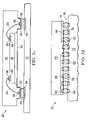
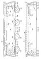
- FIG. 1illustrates electronic device 10 having a chip carrier substrate or printed circuit board (PCB) 12 with a plurality of semiconductor packages or semiconductor die mounted on its surface.
- Electronic device 10may have one type of semiconductor package, or multiple types of semiconductor packages, depending on the application. The different types of semiconductor packages are shown in FIG. 1 for purposes of illustration.
- Electronic device 10may be a stand-alone system that uses the semiconductor packages to perform an electrical function.
- electronic device 10may be a subcomponent of a larger system.
- electronic device 10may be a graphics card, network interface card, or other signal processing card that can be inserted into a computer.
- the semiconductor packagecan include microprocessors, memories, application specific integrated circuits (ASICs), logic circuits, analog circuits, radio frequency (RF) circuits, discrete devices, or other semiconductor die or electrical components.
- ASICsapplication specific integrated circuits
- RFradio frequency
- PCB 12provides a general substrate for structural support and electrical interconnect of the semiconductor packages and other electronic components mounted on the PCB.
- Conductive signal traces 14are formed on a surface or within layers of PCB 12 using evaporation, electrolytic plating, electroless plating, screen printing, or other suitable metal deposition process. Signal traces 14 provide for electrical communication between each of the semiconductor packages, mounted components, and any connected external system components. Traces 14 also provide power and ground connections to each of the semiconductor packages.
- semiconductor packagesincluding a dual in-line package (DIP) 16 , wire-bonded die 18 , bump chip carrier (BCC) 20 , and flip chip package 22 .
- DIPdual in-line package
- BCCbump chip carrier
- flip chip package 22any combination of semiconductor packages or other electronic components can be connected to PCB 12 .
- electronic device 10includes a single attached semiconductor package, while other embodiments call for multiple interconnected packages.
- manufacturerscan incorporate pre-made components into electronic devices and systems. Because the semiconductor packages include sophisticated functionality and represent known good units (KGUs), electronic devices can be manufactured using cheaper components and shorten the manufacturing process. The resulting devices are less likely to fail and less expensive to manufacture resulting in lower costs for consumers.
- KGUsknown good units
- FIG. 2 aillustrates further detail of DIP 16 mounted on PCB 12 .
- DIP 16includes semiconductor die 24 having contact pads 26 .
- Semiconductor die 24includes an active area containing analog or digital circuits implemented as active devices, passive devices, conductive layers, and dielectric layers formed within semiconductor die 24 and are electrically interconnected according to the electrical design of the die.
- the circuitmay include one or more transistors, diodes, inductors, capacitors, resistors, and other circuit elements formed within the active area of die 24 .
- Contact pads 26are made with a conductive material such as aluminum (Al), copper (Cu), tin (Sn), nickel (Ni), gold (Au), or silver (Ag), and are electrically connected to the circuit elements formed within die 24 .
- Contact pads 26are formed by a physical vapor deposition (PVD), chemical vapor deposition (CVD), electrolytic plating, or electroless plating process.
- PVDphysical vapor deposition
- CVDchemical vapor deposition
- electrolytic platingelectroless plating process.
- semiconductor die 24is mounted to a die attach area of lower portion 28 of the package body using a gold-silicon eutectic layer or adhesive material, such as thermal epoxy.
- the package bodyincludes an insulative packaging material such as plastic or ceramic.
- Conductor leads 30are connected to lower portion 28 of the body and bond wires 32 are formed between leads 30 and contact pads 26 of die 24 .
- An encapsulant 34is deposited over the package for environmental protection by preventing moisture and particles from entering the package and contaminating die 24 , contact pads 26 , or bond wires 32 .
- DIP 16is connected to PCB 12 by inserting leads 30 into holes formed through PCB 12 .
- Solder material 36is flowed around leads 30 and into the holes to physically and electrically connect DIP 16 to PCB 12 .
- Solder material 36can be metal or electrically conductive material, e.g., Sn, lead (Pb), Au, Ag, Cu, zinc (Zn), bismuthinite (Bi), and alloys thereof, with an optional flux material.
- the solder materialcan be eutectic Sn/Pb, high lead, or lead free.
- a wire-bonded die 18 having contact pads 38is mounted to PCB 12 using adhesive material 40 .
- Contact pads 42are formed on the surface of PCB 12 and electrically connect to one or more traces 14 formed on or within the layers of PCB 12 .
- Bond wires 44are formed between contact pads 38 of die 18 and contact pads 42 of PCB 12 .
- FIG. 2 cillustrates further detail of BCC 20 with an incorporated semiconductor die, integrated circuit (IC), or combination thereof.
- Semiconductor die 46 having contact pads 48is mounted over a carrier using an underfill or epoxy-resin adhesive material 50 .
- Semiconductor die 46includes an active area containing analog or digital circuits implemented as active devices, passive devices, conductive layers, and dielectric layers formed within semiconductor die 46 and are electrically interconnected according to the electrical design of the die.
- the circuitmay include one or more transistors, diodes, inductors, capacitors, resistors, and other circuit elements formed within the active area of die 46 .
- Contact pads 48are connected to the electrical devices and circuitry formed within the active area of die 46 .
- Bond wires 54 and bond pads 56 and 58electrically connect contact pads 48 of die 46 to contact pads 52 of BCC 20 .
- Mold compound or encapsulant 60is deposited over die 46 , bond wires 54 and contact pads 52 to provide physical support and electrical insulation for the device.
- Contact pads 64are formed on PCB 12 and electrically connect to one or more conductive signal traces 14 .
- Solder materialis deposited between contact pads 52 of BCC 20 and contact pads 64 of PCB 12 . The solder material is ref lowed to form bumps 66 which form a mechanical and electrical connection between BCC 20 and PCB 12 .
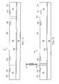
- flip chip style semiconductor device 22has a semiconductor die 72 with active area 70 mounted face down toward PCB 12 .
- Active area 70containing analog or digital circuits implemented as active devices, passive devices, conductive layers, and dielectric layers formed within semiconductor die 72 , is electrically interconnected according to the electrical design of the die.
- the circuitmay include one or more transistors, diodes, inductors, capacitors, resistors, and other circuit elements formed within active area 70 of die 72 .
- the electrical and mechanical interconnectis achieved through solder bump structure 76 comprising a large number of individual conductive solder bumps or balls 78 .
- the solder bumpsare formed on bump pads or interconnect sites 80 , which are disposed on active area 70 .
- the bump pads 80connect to the active circuits by conduction tracks in active area 70 .
- the solder bumps 78are electrically and mechanically connected to contact pads or interconnect sites 82 on PCB 12 by a solder reflow process.
- the interconnect sites 82are electrically connected to one or more conductive signal traces 14 on PCB 12 .
- the flip chip semiconductor deviceprovides a short electrical conduction path from the active devices on die 72 to conduction tracks on PCB 12 in order to reduce signal propagation distance, lower capacitance, and achieve overall better circuit performance.
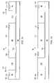
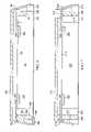
- FIGS. 3 a - 3 hillustrate a process of forming conductive vias in a peripheral region around a semiconductor die in a wafer level chip scale package (WLCSP).
- WLCSPwafer level chip scale package
- the backside of semiconductor die 94is mounted to expansion table 98 with its active surface 106 and contact pads 108 oriented face up.
- the backside of semiconductor die 96is mounted to expansion table 98 with its active surface 110 and contact pads 112 oriented face up.
- Contact pads 104 , 108 , and 112electrically connect to active and passive devices and signal traces in active areas 102 , 106 , and 110 of semiconductor die 92 , 94 , and 96 , respectively.
- Semiconductor die 92 - 96may contain baseband circuits that are susceptible to electromagnetic interference (EMI), radio frequency interference (RFI), or other inter-device interference.
- semiconductor die 92 - 96contain integrated passive devices (IPD) that generate EMI, RFI, and inter-device interference.
- IPDintegrated passive devices
- the IPDs contained within semiconductor die 92 - 96provide the electrical characteristics needed for high frequency applications, such as resonators, high-pass filters, low-pass filters, band-pass filters, symmetric Hi-Q resonant transformers, and tuning capacitors.
- the IPDscan be used as front-end wireless RF components, which can be positioned between the antenna and transceiver.
- the IPD inductorcan be a hi-Q balun, transformer, or coil, operating up to 100 Gigahertz.
- multiple balunsare formed on a same substrate, allowing multi-band operation.
- two or more balunsare used in a quad-band for mobile phones or other global system for mobile (GSM) communications, each balun dedicated for a frequency band of operation of the quad-band device.
- the output signal in the transmitter section of the radio frequency integrated circuit (RFIC)may interfere with the local oscillator (LO).
- the inductorcan be used in the tank resonators of the LO in the RF transceiver.
- the LOincludes a voltage-controlled oscillator (VCO) that is synchronized to an external crystal reference through a phase-locked loop (PLL).
- VCOvoltage-controlled oscillator
- PLLphase-locked loop
- the VCOcan be implemented as a cross-coupled amplifier circuit with a tuned resonant inductor-capacitor (LC) load.
- the inductoris made with one or two spiral inductor coils on the RFIC.
- External signalscan couple into the VCO by magnetic induction directly into the tank resonator. If the external source is a periodic or quasi-periodic signal, it will introduce a spurious tone.
- the RF signalis multiplied by the LO signal to transpose the band of interest down to low frequency for further signal processing.
- a saw blade or laser tool 114cuts through saw street 116 between semiconductor die 92 and 94 , and through saw street 116 between semiconductor die 94 and 96 , in a dicing operation.
- Expansion table 98moves in two-dimension lateral directions, as shown by arrows 118 in FIG. 3 c , to expand the width of saw streets 116 , i.e., form a gap to create a greater physical separation between the die.
- Expansion table 98moves substantially the same distance in the x-axis and y-axis to provide equal separation around a peripheral region of each die.
- the post-expansion width of saw street or gap 116ranges from 5 micrometers ( ⁇ m) to 200 ⁇ m.
- the expanded dimensiondepends on the design embodiment, i.e., half-via, full-via, single row via, or double/multiple row via.
- the expanded saw street or gap 116define a peripheral region around the semiconductor die.
- the semiconductor waferis diced to separate the semiconductor die.
- the individual semiconductor dieare then transferred and affixed to a temporary chip carrier with an adhesive layer, e.g., thermal epoxy.
- the semiconductor dieare placed on the chip carrier so as to have a predetermined separation gap.
- the separation gaphas sufficient width to form conductive vias within the gap, as described below.
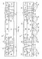
- an organic insulating material 120is deposited in gap 116 using spin coating, needle dispensing, or other suitable application process.
- Organic material 120can be benzocyclobutene (BCB), polyimide (PI), or acrylic resin.
- BCBbenzocyclobutene
- PIpolyimide
- acrylic resinacrylic resin
- other non-conductive materialssuch as a polymer molding compound, liquid epoxy molding, compression molding, soft laminating film, or other material having dielectric or electrical insulating properties can be deposited in gap 116 .
- the non-conductive materialscan also be deposited using a transfer molding or injection molding process.
- a portion of organic material 120is removed by laser drilling or etching to create openings that extend down to expansion table 98 .
- the openingscan be vertical or tapered.
- An electrically conductive materialis deposited into the openings to form conductive though hole vias (THV) 122 and 123 using a PVD, CVD, evaporation, electrolytic plating, electroless plating, screen printing, or other suitable metal deposition process.
- the conductive materialcan be made with metals such as Al, Cu, Sn, Ni, Au, Ag, or other suitable electrically conductive material.
- An electrically conductive layer 124is patterned and deposited on active surfaces 102 , 106 , and 110 of semiconductor die 92 , 94 , and 96 , respectively, as well as organic material 120 .
- Conductive layer 124can be deposited by using a PVD, CVD, evaporation, electrolytic plating, electroless plating, screen printing, or other suitable metal deposition process.
- Conductive layer 124can be made with Al, Cu, Sn, Ni, Au, Ag, or other suitable electrically conductive material.
- Conductive layer 124is a redistribution layer (RDL) that electrically connects contact pads 104 , 108 , and 112 to THVs 122 and 123 as shown.
- RDLredistribution layer
- An insulating material 126is formed over the active surfaces of semiconductor die 92 - 96 and conductive layer 124 for structural support and physical isolation.
- the insulating layer 126can be made with nitride (SiN), silicon dioxide (SiO2), silicon oxynitride (SiON), tantalum pentoxide (Ta2O5), zircon (ZrO2), aluminum oxide (Al2O3), polyimide (PI), benzocyclobutene (BCB), polybenzoxazole (PBO), or other suitable insulating material.
- the deposition of insulating layer 126may involve PVD, CVD, printing, sintering, or thermal oxidation.
- a tapered or V-shaped profile 128is formed in insulating layer 126 and organic material 120 using an etching process.
- Profile 128extends down to expansion table 98 .
- profile 128can be truncated V-shape, vertical, flat, or curved in shape.
- Another portion of insulating layer 126is removed using an etching process to form opening 130 and expose conductive layer 124 over conductive THV 123 .
- an electrically conductive shielding layer 132 with an optional seed layeris conformally deposited over insulating layer 126 and organic material 120 .
- Shielding layer 132extends into profile 128 and opening 130 and electrically connects to conductive layer 124 and conductive THV 123 .
- Shielding layer 132can be Cu, Al, stainless steel, nickel silver, low-carbon steel, silicon-iron steel, foil, epoxy, conductive resin, and other metals and composites capable of blocking EMI, RFI, and other externally generated interference.
- the seed layercan be made with Cu, Ni, nickel vanadium (NiV), Au, or Al.
- the seed layer and shielding layer 132are patterned and conformally deposited using an electrolytic plating, electroless plating, sputtering, PVD, CVD, or other suitable metal deposition process.
- shielding layer 132can be applied by lamination, spraying, or painting.
- Shielding layer 132substantially covers all areas of insulating layer 126 relative to the top of semiconductor die 92 - 96 to provide isolation from EMI, RFI, or other inter-device interference.
- the interferencecan be generated internally or originating from external semiconductor devices containing IPDs or RF circuits.
- the shielding layeralso isolates the sides of semiconductor die 92 - 96 from EMI, RFI, or other inter-device interference.
- Organic material 120 and insulating layer 126must be sufficiently thick to maintain structural integrity of conductive THVs 122 and 123 and conductive layer 124 after depositing shielding layer 132 .
- a thick insulating layer 126also reduces crosstalk and other interference between shielding layer 132 and conductive layer 124 .
- semiconductor wafer 90is removed from expansion table 98 .
- An interconnect structureis formed on a backside of semiconductor die 92 - 96 , opposite active surfaces 102 , 106 , and 110 .
- the interconnect structureincludes an electrically conductive layer which is patterned and deposited to form RDL 134 .
- Conductive layer 134can be deposited by using a PVD, CVD, evaporation, electrolytic plating, electroless plating, screen printing, or other suitable metal deposition process.
- Conductive layer 134can be made with Al, Cu, Sn, Ni, Au, Ag, or other suitable electrically conductive material.
- RDL 134electrically connects to conductive THVs 122 and 123 .
- An insulating layer 136is formed over RDL 134 and the backside of semiconductor die 92 - 96 for structural support and physical isolation.
- the insulating layer 136can be made with Si3N4, SiO2, SiON, Ta2O5, zirconium oxide (ZrO2), or other suitable dielectric material.
- the deposition of insulating layer 136may involve PVD, CVD, printing, sintering, or thermal oxidation. A portion of insulating layer 136 is removed by an etching process to expose RDL 134 . Contact pads 137 are then formed on RDL 134 .
- solder materialis deposited over contact pads 137 using an evaporation, electrolytic plating, electroless plating, ball drop, or screen printing process.
- the solder materialcan be metal or electrically conductive material, e.g., Sn, Pb, Ni, Au, Ag, Cu, Bi, and alloys thereof.
- the solder materialcan be eutectic Sn/Pb, high lead, or lead free.
- the solder materialis ref lowed by heating the solder material above its melting point to form solder bumps 138 and 140 . In some applications, solder bumps 138 and 140 are ref lowed a second time to improve electrical contact to contact pads 137 .
- Solder bumps 140are electrically connected to an external low-impedance ground point to aid in the shielding feature of layer 132 .
- bond wires or solder pastecan be used for the external interconnect including the ground connection.
- Semiconductor die 92 - 96are singulated through a center portion of gap 116 , i.e., through a center portion of profile 128 .
- the gap region 116is cut by a cutting tool such as a saw blade or laser. The cutting tool completely severs the gap region to separate the die.
- FIG. 4shows a final configuration for semiconductor die 94 .
- Contact pads 108electrically connect through conductive layer 124 to conductive THVs 122 and 123 which are formed in organic material 120 .
- Shielding layer 132is formed over insulating layer 126 .
- Shielding layer 132also conforms to V-shaped profile 128 .
- Shielding layer 132electrically connects to an external ground point through conductive layer 124 , conductive THVs 123 , RDL 134 , contact pads 137 , and solder bump 140 .
- Shielding layer 132substantially covers all areas of insulating layer 126 relative to the top of semiconductor die 92 - 96 to provide isolation from EMI, RFI, or other inter-device interference.
- the shielding layeralso isolates the sides of semiconductor die 94 from EMI, RFI, or other inter-device interference.
- Other electrical signalsare routed to and from semiconductor die 94 through contact pads 108 , conductive layer 124 , conductive THV 122 , RDL 134 , contact pads 137 , and solder bumps 138 .
- semiconductor die 150includes contact pads 152 which are electrically connected through conductive layer 154 to conductive THVs 156 and 158 which are formed in organic material 160 .
- Conductive THVs 156 and 158protrude into insulating material 164 .
- Shielding layer 162is formed over insulating layer 164 .
- Shielding layer 162also conforms to V-shaped profile 166 .
- Shielding layer 162electrically connects to an external ground point through conductive THV 156 . In this embodiment, the external interconnectivity is achieved directly through protruding conductive THVs 156 and 158 .
- Shielding layer 162substantially covers all areas of insulating layer 164 relative to the top of semiconductor die 150 to provide isolation from EMI, RFI, or other inter-device interference.
- profile 166being cut into organic material 160 and shielding layer 162 extending into the profile, the shielding layer also isolates the sides of semiconductor die 150 from EMI, RFI, or other inter-device interference.
- Other electrical signalsare routed to and from semiconductor die 150 through contact pads 152 , conductive layer 154 , and conductive THV 158 .
- FIG. 6shows semiconductor die 180 with contact pads 182 electrically connected through conductive layer 184 to conductive THVs 186 and 188 which are formed in organic material 190 .
- Shielding layer 192is formed over insulating layer 194 .
- Shielding layer 192also conforms to V-shaped profile 186 .
- a backside RDL 198electrically connects to an external ground point.
- shielding layer 182electrically connects to the external ground point through RDL 198 .
- Shielding layer 192substantially covers all areas of insulating layer 194 relative to the top of semiconductor die 180 to provide isolation from EMI, RFI, or other inter-device interference.
- the shielding layerBy virtue of profile 196 being cut into organic material 190 and shielding layer 192 extending into the profile, the shielding layer also isolates the sides of semiconductor die 180 from EMI, RFI, or other inter-device interference. Other electrical signals are routed to and from semiconductor die 180 through contact pads 182 , conductive layer 184 , and conductive THV 188 .
- semiconductor die 200includes contact pads 202 electrically connected through conductive layer 204 to conductive THVs 206 and 208 which are formed in organic material 210 .
- Shielding layer 212is formed over insulating layer 214 .
- Shielding layer 212also conforms to V-shaped profile 216 .
- a portion of shielding layer 212 and insulating layer 214is removed by an etching process to form opening 218 and expose conductive layer 204 over conductive THV 208 . Opening 218 can be circular, rectangular, oval, or other irregular shapes.
- Shielding layer 212electrically connects to an external ground point through conductive layer 204 and conductive THV 206 .
- Shielding layer 212substantially covers all areas of insulating layer 214 relative to the top of semiconductor die 200 to provide isolation from EMI, RFI, or other inter-device interference.
- profile 216being cut into organic material 210 and shielding layer 212 extending into the profile, the shielding layer also isolates the sides of semiconductor die 200 from EMI, RFI, or other inter-device interference.
- Other electrical signalsare routed to and from semiconductor die 200 through contact pads 202 , conductive layer 204 , and conductive THV 208 . Opening 218 provides interconnect access to conductive layer 204 for stacking semiconductor die.
- the aforedescribed semiconductor die covered by the shielding layercan be readily integrated into package-in-package (PiP) applications, as shown in FIG. 8 .
- Semiconductor die 220includes contact pads 222 electrically connected through conductive layer 224 to conductive THVs 226 and 228 which are formed in the organic material occupying the peripheral region around semiconductor die 220 .
- Shielding layer 230is formed over insulating layer 232 .
- Shielding layer 230also conforms to the V-shaped profile which is also formed in the organic material occupying the peripheral region around semiconductor die 220 .
- Shielding layer 230substantially covers all areas of insulating layer 232 relative to the top of semiconductor die 220 to provide isolation from EMI, RFI, or other inter-device interference.
- the shielding layeralso isolates the sides of semiconductor die 220 from EMI, RFI, or other inter-device interference.
- Semiconductor die 240includes contact pads 242 electrically connected through conductive layer 244 to conductive THVs 246 and 248 which are formed in the organic material occupying the peripheral region around semiconductor die 240 .
- Shielding layer 250is formed over insulating layer 252 .
- Shielding layer 250also conforms to the V-shaped profile which is formed in the organic material occupying the peripheral region around semiconductor die 240 .
- Shielding layer 250substantially covers all areas of insulating layer 252 relative to the top of semiconductor die 240 to provide isolation from EMI, RFI, or other inter-device interference.
- the shielding layeralso isolates the sides of semiconductor die 240 from EMI, RFI, or other inter-device interference.
- Semiconductor die 220 and 240are vertically stacked and electrically connected by solder bumps 254 and 256 and interconnect structure and RDL 258 and 259 . Alternately, semiconductor die 220 and 240 can be electrically interconnected with solder paste. Semiconductor die 220 and 240 can be the same size or different size.
- the stacked semiconductor dieare mounted to a top side of substrate 260 with an adhesive layer 261 , such as thermal epoxy, polymer composite, or inorganic bonding compounds.
- Substrate 260can be laminate, embedded die substrate, ceramics, or leadframe.
- Substrate 260has an interconnect structure 262 including signal traces, conductive layers, and dielectric layers. Contact pads 266 are formed on a backside of substrate 260 with electrical connection to interconnect structure 262 . Solder bumps 268 and 270 are formed on contact pads 266 .
- Shielding layer 230electrically connects to shielding layer 250 through conductive layer 224 , conductive THV 226 , solder bump 254 , RDL 259 , conductive THV 246 , and conductive layer 244 .
- Shielding layer 250electrically connects to an external ground point through interconnect structure 262 , contact pads 266 and solder bumps 268 .
- shielding layers 230 and 250are both connected to the external ground point through a common conductive path, i.e., interconnect structure 262 , contact pads 266 and solder bump 268 .
- Other electrical signalsare routed to and from semiconductor die 220 and 240 through contact pads 222 and 242 , conductive layers 224 and 244 , conductive THVs 228 and 248 , solder bumps 256 , and RDL 258 .
- the electrical signalsare also routed to substrate 260 through bond wires 272 connected to RDLs 258 . Bond wires 272 electrically connect to interconnect structure 262 , contact pads 266 , and solder bumps 270 for external interconnectivity of the electrical signals.
- FIG. 9shows another PiP embodiment where each shielding layer has a separate electrical connection to the external ground point.
- Semiconductor die 280includes contact pads 282 electrically connected through conductive layer 284 to conductive THVs 286 and 288 which are formed in the organic material occupying the peripheral region around semiconductor die 280 .
- Shielding layer 290is formed over insulating layer 292 .
- Shielding layer 290also conforms to the V-shaped profile which is also formed in the organic material occupying the peripheral region around semiconductor die 280 .
- Shielding layer 290substantially covers all areas of insulating layer 292 relative to the top of semiconductor die 280 to provide isolation from EMI, RFI, or other inter-device interference.
- the shielding layeralso isolates the sides of semiconductor die 280 from EMI, RFI, or other inter-device interference.
- Semiconductor die 300includes contact pads 302 electrically connected through conductive layer 304 to conductive THVs 306 and 308 which are formed in the organic material occupying the peripheral region around semiconductor die 300 .
- Shielding layer 310is formed over insulating layer 312 .
- Shielding layer 310also conforms to the V-shaped profile which is formed in the organic material occupying the peripheral region around semiconductor die 300 .
- Shielding layer 310substantially covers all areas of insulating layer 312 relative to the top of semiconductor die 300 to provide isolation from EMI, RFI, or other inter-device interference.
- the shielding layeralso isolates the sides of semiconductor die 300 from EMI, RFI, or other inter-device interference.
- Semiconductor die 280 and 300are vertically stacked and bonded with an adhesive layer 314 , such as thermal epoxy, polymer composite, or inorganic bonding compounds. A portion of shielding layer 310 and insulating layer 312 is removed to form an opening like 218 in FIG. 7 .
- Solder bump 316is formed in the opening to electrically connect conductive THVs 288 and 308 and route electrical signals between semiconductor die 280 and 300 .
- Solder bump 316is electrically isolated from shielding layers 290 and 310 .
- An interconnect structureis formed on the backside of semiconductor die 300 , including RDLs 320 , insulating layer 322 , contact pads 324 , and solder bumps 326 and 328 .
- the stacked semiconductor dieare mounted to a top side of substrate 330 with solder bumps 326 and 328 contacting interconnect structure 332 .
- Substrate 330can be laminate, embedded die substrate, ceramics, or leadframe.
- the interconnect structure 332includes signal traces, conductive layers, and dielectric layers.
- Contact pads 336are formed on a backside of substrate 330 with electrical connection to interconnect structure 332 .
- Solder bumps 338 , 340 , and 342are formed on contact pads 336 .
- Shielding layer 290electrically connects to an external ground point through bond wire 334 , interconnect structure 332 , contact pads 336 , and solder bumps 340 .
- Shielding layer 310electrically connects to an external ground point through conductive layer 304 , conductive THV 306 , RDL 320 , contact pad 324 , solder bump 326 , interconnect structure 332 , contact pads 336 , and solder bumps 328 . Accordingly, shielding layers 290 and 310 are connected to external ground points through separate conductive paths.
- Other electrical signalsare routed to and from semiconductor die 280 and 300 through contact pads 282 and 302 , conductive layers 284 and 304 , conductive THVs 288 and 308 , and solder bump 316 .
- the electrical signalsare further routed through RDL 320 , contact pad 324 , solder bumps 328 , interconnect structure 332 , contact pad 336 , and solder bumps 342 for external interconnectivity.
- a molding compound or encapsulant 344is deposited over semiconductor device 280 and 300 , bond wires 334 , and substrate 330 .
- Molding compound 344can be made with epoxy acrylate or other polymer material and applied by transfer molding, liquid encapsulant molding, or other molding process. Molding compound 344 is non-conductive and environmentally protects the semiconductor device from external elements and contaminants.
- FIG. 10shows another PiP embodiment where the shielding layers have a common electrical connection to the external ground point.
- Semiconductor die 350includes contact pads 352 electrically connected through conductive layer 354 to conductive THVs 356 and 358 which are formed in the organic material occupying the peripheral region around semiconductor die 350 .
- Shielding layer 360is formed over insulating layer 362 .
- Shielding layer 360also conforms to the V-shaped profile which is also formed in the organic material occupying the peripheral region around semiconductor die 350 .
- Shielding layer 360substantially covers all areas of insulating layer 362 relative to the top of semiconductor die 350 to provide isolation from EMI, RFI, or other inter-device interference.
- the shielding layeralso isolates the sides of semiconductor die 350 from EMI, RFI, or other inter-device interference.
- Semiconductor die 370include contact pads 372 electrically connected through conductive layer 374 to conductive THVs 376 and 378 which are formed in the organic material occupying the peripheral region around semiconductor die 370 .
- Shielding layer 380is formed over insulating layer 382 .
- Shielding layer 380also conforms to the V-shaped profile which is formed in the organic material occupying the peripheral region around semiconductor die 370 .
- Shielding layer 380substantially covers all areas of insulating layer 382 relative to the top of semiconductor die 370 to provide isolation from EMI, RFI, or other inter-device interference.
- the shielding layeralso isolates the sides of semiconductor die 370 from EMI, RFI, or other inter-device interference.
- Semiconductor die 350 and 370are vertically stacked and electrically connected with solder bumps 384 and 386 .
- a portion of shielding layer 380 and insulating layer 382is removed to form an opening like 218 in FIG. 7 .
- Solder bump 386is electrically isolated from shielding layers 360 and 380 .
- Solder bump 386is formed in the opening to electrically connect conductive THVs 358 and 378 and route electrical signals between semiconductor die 350 and 370 .
- An interconnect structureis formed on the backside of semiconductor die 370 , including RDLs 390 , insulating layer 392 , contact pads 394 , and solder bumps 396 and 398 .
- the stacked semiconductor dieare mounted to a top side of substrate 400 with solder bumps 396 and 398 contacting interconnect structure 402 .
- Substrate 400can be laminate, embedded die substrate, ceramics, or leadframe.
- the interconnect structure 402includes signal traces, conductive layers, and dielectric layers.
- Contact pads 404are formed on a backside of substrate 400 with electrical connection to interconnect structure 402 .
- Solder bumps 406 and 408are formed on contact pads 404 .
- Shielding layer 360electrically connects shielding layer 380 through conductive layer 354 , conductive THV 356 , and solder bump 384 .
- Shielding layer 380electrically connects to an external ground point through conductive layer 374 , conductive THV 376 , RDL 390 , contact pad 394 , solder bump 398 , interconnect structure 402 , contact pads 404 , and solder bumps 406 .
- shielding layers 360 and 380are both connected to the external ground point through a common conductive path, i.e., RDL 390 , contact pad 394 , solder bump 398 , interconnect structure 402 , contact pads 404 , and solder bumps 406 .
- Other electrical signalsare routed to and from semiconductor die 350 and 370 through contact pads 352 and 372 , conductive layers 354 and 374 , conductive THVs 358 and 378 , and solder bump 386 .
- the electrical signalsare further routed through RDL 390 , contact pad 394 , solder bumps 396 , interconnect structure 402 , contact pad 404 , and solder bumps 408 for external interconnectivity.
- a molding compound or encapsulant 410is deposited over semiconductor device 350 and 370 and substrate 400 .
- Molding compound 410can be made with epoxy acrylate or other polymer material and applied by transfer molding, liquid encapsulant molding, or other molding process. Molding compound 410 is non-conductive and environmentally protects the semiconductor device from external elements and contaminants.
Landscapes
- Engineering & Computer Science (AREA)
- Microelectronics & Electronic Packaging (AREA)
- Power Engineering (AREA)
- Computer Hardware Design (AREA)
- Physics & Mathematics (AREA)
- General Physics & Mathematics (AREA)
- Condensed Matter Physics & Semiconductors (AREA)
- Manufacturing & Machinery (AREA)
- Health & Medical Sciences (AREA)
- Electromagnetism (AREA)
- Toxicology (AREA)
- Semiconductor Integrated Circuits (AREA)
- Internal Circuitry In Semiconductor Integrated Circuit Devices (AREA)
Abstract
Description
- The present application is a division of U.S. patent application Ser. No. 12/140,092, filed Jun. 16, 2008, and claims priority to the foregoing parent application pursuant to 35 U.S.C. § 120.
- The present invention relates in general to semiconductor devices and, more particularly, to a semiconductor device and method of forming a shielding layer along a profile disposed in a peripheral region around the device.
- Semiconductor devices are found in many products in the fields of entertainment, communications, networks, computers, and household markets. Semiconductor devices are also found in military, aviation, automotive, industrial controllers, and office equipment. The semiconductor devices perform a variety of electrical functions necessary for each of these applications.
- The manufacture of semiconductor devices involves formation of a wafer having a plurality of die. Each semiconductor die contains hundreds or thousands of transistors and other active and passive devices performing a variety of electrical functions. For a given wafer, each die from the wafer typically performs the same electrical function. Front-end manufacturing generally refers to formation of the semiconductor devices on the wafer. The finished wafer has an active side containing the transistors and other active and passive components. Back-end manufacturing refers to cutting or singulating the finished wafer into the individual die and then packaging the die for structural support and environmental isolation.
- One goal of semiconductor manufacturing is to produce a package suitable for faster, reliable, smaller, and higher-density integrated circuits (IC) at lower cost. Flip chip packages or wafer level chip scale packages (WLCSP) are ideally suited for ICs demanding high speed, high density, and greater pin count. Flip chip style packaging involves mounting the active side of the die face down toward a chip carrier substrate or printed circuit board (PCB). The electrical and mechanical interconnect between the active devices on the die and conduction tracks on the carrier substrate is achieved through a solder bump structure comprising a large number of conductive solder bumps or balls. The solder bumps are formed by a reflow process applied to solder material deposited on contact pads, which are disposed on the semiconductor substrate. The solder bumps are then soldered to the carrier substrate. The flip chip semiconductor package provides a short electrical conduction path from the active devices on the die to the carrier substrate in order to reduce signal propagation, lower capacitance, and achieve overall better circuit performance.
- In many applications, it is desirable to vertically stack semiconductor die for greater device integration and minimize interconnect routing. The electrical interconnection between stacked semiconductor die has been done by using through hole vias which traverse from a front side to the backside of the die. The through hole vias are formed by drilling through the active area of the die or through saw streets on the wafer prior to any dicing operation. The through hole vias are filled with conductive material. The process of drilling through hole vias in the active area of the die or in saw streets on the wafer can cause damage to the wafer and/or die.
- In high frequency applications, such as radio frequency (RF) wireless communications, integrated passive devices (IPDs) are often contained within the semiconductor device. Examples of IPDs include resistors, capacitors, and inductors. A typical RF system requires multiple IPDs in one or more semiconductor packages to perform the necessary electrical functions. However, high frequency electrical devices generate undesired electromagnetic interference (EMI) and radio frequency interference (RFI), or other inter-device interference, such as capacitive, inductive, or conductive coupling, also known as cross-talk, which can interfere with the operation of adjacent circuit elements.
- A need exists for a stackable semiconductor device with a shielding layer and conductive via formed in a peripheral region around the device. Accordingly, in one embodiment, the present invention is a semiconductor device comprising a semiconductor die having a peripheral region around the semiconductor die. A first insulating material is deposited in the peripheral region. A conductive via is formed through the first insulating material in the peripheral region. A conductive layer is formed over the first insulating layer and semiconductor die. The conductive layer is electrically connected to the conductive via and a contact pad of the semiconductor die. A second insulating layer is deposited over the first insulating layer, conductive layer, and semiconductor die. The first and second insulating layers have a profile formed in the peripheral region around the semiconductor die. An opening is formed in the second insulating layer to expose the conductive layer. A shielding layer is formed over the first and second insulating layers to isolate the semiconductor die from inter-device interference. The shielding layer conforms to the profile in the peripheral region around the semiconductor die and to the opening to electrically connect the shielding layer to the conductive via.
- In another embodiment, the present invention is a semiconductor device comprising a semiconductor die having a peripheral region around the semiconductor die. A first insulating material is deposited in the peripheral region. A conductive via is formed through the first insulating material in the peripheral region. A second insulating layer is deposited over the first insulating layer and semiconductor die. The first and second insulating layers have a profile formed in the peripheral region around the semiconductor die. A shielding layer is formed over the first and second insulating layers to isolate the semiconductor die from inter-device interference. The shielding layer conforms to the profile in the peripheral region around the semiconductor die and is electrically connected to the conductive via.
- In another embodiment, the present invention is a semiconductor device comprising a semiconductor die having a peripheral region. A first insulating material is deposited in the peripheral region. A conductive via is formed through the first insulating material. A second insulating layer is deposited over the first insulating layer and semiconductor die. The first and second insulating layers have a profile formed in the peripheral region around the semiconductor die. A shielding layer is formed over the first and second insulating layers to isolate the semiconductor die from inter-device interference. The shielding layer conforms to the profile in the peripheral region around the semiconductor die.
- In another embodiment, the present invention is a semiconductor device comprising a semiconductor die having a peripheral region. A first insulating material is formed in the peripheral region. A conductive via is formed through the first insulating material in the peripheral region around the semiconductor die. A second insulating layer is formed over the first insulating layer and semiconductor die. A shielding layer is formed over the first and second insulating layers to isolate the semiconductor die from inter-device interference.
FIG. 1 illustrates a PCB with different types of packages mounted to its surface;FIGS. 2 a-2dillustrate further detail of the semiconductor packages mounted to the PCB;FIGS. 3 a-3hillustrate a process of forming a shielding layer formed along a V-shaped profile in peripheral region around the die;FIG. 4 illustrates the semiconductor device with a shielding layer formed along V-shaped profile and having a backside interconnect structure;FIG. 5 illustrates the semiconductor device with a shielding layer formed along V-shaped profile and having an interconnect through conductive vias;FIG. 6 illustrates the semiconductor device with a shielding layer formed along V-shaped profile and having an interconnect through conductive vias and backside RDL;FIG. 7 illustrates the semiconductor device with a shielding layer formed along V-shaped profile and having an opening over conductive vias;FIG. 8 illustrates vertically stacked semiconductor die each with a shielding layer formed along V-shaped profile;FIG. 9 illustrates vertically stacked semiconductor die each with a shielding layer formed along V-shaped profile and having separate connection to external ground point; andFIG. 10 illustrates vertically stacked semiconductor die each with a shielding layer formed along V-shaped profile and having common connection to external ground point.- The present invention is described in one or more embodiments in the following description with reference to the Figures, in which like numerals represent the same or similar elements. While the invention is described in terms of the best mode for achieving the invention's objectives, it will be appreciated by those skilled in the art that it is intended to cover alternatives, modifications, and equivalents as may be included within the spirit and scope of the invention as defined by the appended claims and their equivalents as supported by the following disclosure and drawings.
- The manufacture of semiconductor devices involves formation of a wafer having a plurality of die. Each die contains hundreds or thousands of transistors and other active and passive devices performing one or more electrical functions. For a given wafer, each die from the wafer typically performs the same electrical function. Front-end manufacturing generally refers to formation of the semiconductor devices on the wafer. The finished wafer has an active side containing the transistors and other active and passive components. Back-end manufacturing refers to cutting or singulating the finished wafer into the individual die and then packaging the die for structural support and/or environmental isolation.
- A semiconductor wafer generally includes an active surface having semiconductor devices disposed thereon, and a backside surface formed with bulk semiconductor material, e.g., silicon. The active side surface contains a plurality of semiconductor die. The active surface is formed by a variety of semiconductor processes, including layering, patterning, doping, and heat treatment. In the layering process, semiconductor materials are grown or deposited on the substrate by techniques involving thermal oxidation, nitridation, chemical vapor deposition, evaporation, and sputtering. Photolithography involves the masking of areas of the surface and etching away undesired material to form specific structures. The doping process injects concentrations of dopant material by thermal diffusion or ion implantation.
FIG. 1 illustrateselectronic device 10 having a chip carrier substrate or printed circuit board (PCB)12 with a plurality of semiconductor packages or semiconductor die mounted on its surface.Electronic device 10 may have one type of semiconductor package, or multiple types of semiconductor packages, depending on the application. The different types of semiconductor packages are shown inFIG. 1 for purposes of illustration.Electronic device 10 may be a stand-alone system that uses the semiconductor packages to perform an electrical function. Alternatively,electronic device 10 may be a subcomponent of a larger system. For example,electronic device 10 may be a graphics card, network interface card, or other signal processing card that can be inserted into a computer. The semiconductor package can include microprocessors, memories, application specific integrated circuits (ASICs), logic circuits, analog circuits, radio frequency (RF) circuits, discrete devices, or other semiconductor die or electrical components.- In
FIG. 1 ,PCB 12 provides a general substrate for structural support and electrical interconnect of the semiconductor packages and other electronic components mounted on the PCB. Conductive signal traces14 are formed on a surface or within layers ofPCB 12 using evaporation, electrolytic plating, electroless plating, screen printing, or other suitable metal deposition process. Signal traces14 provide for electrical communication between each of the semiconductor packages, mounted components, and any connected external system components.Traces 14 also provide power and ground connections to each of the semiconductor packages. - For the purpose of illustration, several types of semiconductor packages, including a dual in-line package (DIP)16, wire-bonded
die 18, bump chip carrier (BCC)20, andflip chip package 22, are shown mounted onPCB 12. Depending upon the system requirements, any combination of semiconductor packages or other electronic components can be connected toPCB 12. In some embodiments,electronic device 10 includes a single attached semiconductor package, while other embodiments call for multiple interconnected packages. By combining one or more semiconductor packages over a single substrate, manufacturers can incorporate pre-made components into electronic devices and systems. Because the semiconductor packages include sophisticated functionality and represent known good units (KGUs), electronic devices can be manufactured using cheaper components and shorten the manufacturing process. The resulting devices are less likely to fail and less expensive to manufacture resulting in lower costs for consumers. FIG. 2 aillustrates further detail ofDIP 16 mounted onPCB 12.DIP 16 includes semiconductor die24 havingcontact pads 26. Semiconductor die24 includes an active area containing analog or digital circuits implemented as active devices, passive devices, conductive layers, and dielectric layers formed within semiconductor die24 and are electrically interconnected according to the electrical design of the die. For example, the circuit may include one or more transistors, diodes, inductors, capacitors, resistors, and other circuit elements formed within the active area ofdie 24. Contactpads 26 are made with a conductive material such as aluminum (Al), copper (Cu), tin (Sn), nickel (Ni), gold (Au), or silver (Ag), and are electrically connected to the circuit elements formed withindie 24. Contactpads 26 are formed by a physical vapor deposition (PVD), chemical vapor deposition (CVD), electrolytic plating, or electroless plating process. During assembly ofDIP 16, semiconductor die24 is mounted to a die attach area oflower portion 28 of the package body using a gold-silicon eutectic layer or adhesive material, such as thermal epoxy. The package body includes an insulative packaging material such as plastic or ceramic. Conductor leads30 are connected tolower portion 28 of the body andbond wires 32 are formed betweenleads 30 andcontact pads 26 ofdie 24. Anencapsulant 34 is deposited over the package for environmental protection by preventing moisture and particles from entering the package and contaminatingdie 24,contact pads 26, orbond wires 32.DIP 16 is connected toPCB 12 by insertingleads 30 into holes formed throughPCB 12.Solder material 36 is flowed around leads30 and into the holes to physically and electrically connectDIP 16 toPCB 12.Solder material 36 can be metal or electrically conductive material, e.g., Sn, lead (Pb), Au, Ag, Cu, zinc (Zn), bismuthinite (Bi), and alloys thereof, with an optional flux material. For example, the solder material can be eutectic Sn/Pb, high lead, or lead free.- Referring to
FIG. 2 b, a wire-bondeddie 18 havingcontact pads 38 is mounted toPCB 12 usingadhesive material 40. Contactpads 42 are formed on the surface ofPCB 12 and electrically connect to one ormore traces 14 formed on or within the layers ofPCB 12.Bond wires 44 are formed betweencontact pads 38 ofdie 18 andcontact pads 42 ofPCB 12. FIG. 2 cillustrates further detail ofBCC 20 with an incorporated semiconductor die, integrated circuit (IC), or combination thereof. Semiconductor die46 havingcontact pads 48 is mounted over a carrier using an underfill or epoxy-resin adhesive material 50. Semiconductor die46 includes an active area containing analog or digital circuits implemented as active devices, passive devices, conductive layers, and dielectric layers formed within semiconductor die46 and are electrically interconnected according to the electrical design of the die. For example, the circuit may include one or more transistors, diodes, inductors, capacitors, resistors, and other circuit elements formed within the active area ofdie 46. Contactpads 48 are connected to the electrical devices and circuitry formed within the active area ofdie 46.Bond wires 54 andbond pads contact pads 48 ofdie 46 to contactpads 52 ofBCC 20. Mold compound orencapsulant 60 is deposited overdie 46,bond wires 54 andcontact pads 52 to provide physical support and electrical insulation for the device. Contactpads 64 are formed onPCB 12 and electrically connect to one or more conductive signal traces14. Solder material is deposited betweencontact pads 52 ofBCC 20 andcontact pads 64 ofPCB 12. The solder material is ref lowed to formbumps 66 which form a mechanical and electrical connection betweenBCC 20 andPCB 12.- In
FIG. 2 d, flip chipstyle semiconductor device 22 has asemiconductor die 72 withactive area 70 mounted face down towardPCB 12.Active area 70 containing analog or digital circuits implemented as active devices, passive devices, conductive layers, and dielectric layers formed within semiconductor die72, is electrically interconnected according to the electrical design of the die. For example, the circuit may include one or more transistors, diodes, inductors, capacitors, resistors, and other circuit elements formed withinactive area 70 ofdie 72. The electrical and mechanical interconnect is achieved throughsolder bump structure 76 comprising a large number of individual conductive solder bumps orballs 78. The solder bumps are formed on bump pads orinterconnect sites 80, which are disposed onactive area 70. Thebump pads 80 connect to the active circuits by conduction tracks inactive area 70. The solder bumps78 are electrically and mechanically connected to contact pads orinterconnect sites 82 onPCB 12 by a solder reflow process. Theinterconnect sites 82 are electrically connected to one or more conductive signal traces14 onPCB 12. The flip chip semiconductor device provides a short electrical conduction path from the active devices on die72 to conduction tracks onPCB 12 in order to reduce signal propagation distance, lower capacitance, and achieve overall better circuit performance. FIGS. 3 a-3hillustrate a process of forming conductive vias in a peripheral region around a semiconductor die in a wafer level chip scale package (WLCSP). To start the process, a plurality of semiconductor die is formed on asemiconductor wafer 90 using conventional integrated circuit processes, as described above. The first semiconductor wafer, containing semiconductor die92,94, and96, is mounted to expansion table98 with ultraviolet (UV)tape 100, as shown inFIG. 3 a. The backside of semiconductor die92 is affixed to expansion table98 with itsactive surface 102 andcontact pads 104 oriented face up. Likewise, the backside of semiconductor die94 is mounted to expansion table98 with itsactive surface 106 andcontact pads 108 oriented face up. The backside of semiconductor die96 is mounted to expansion table98 with itsactive surface 110 andcontact pads 112 oriented face up. Contactpads active areas - Semiconductor die92-96 may contain baseband circuits that are susceptible to electromagnetic interference (EMI), radio frequency interference (RFI), or other inter-device interference. In other embodiments, semiconductor die92-96 contain integrated passive devices (IPD) that generate EMI, RFI, and inter-device interference. For example, the IPDs contained within semiconductor die92-96 provide the electrical characteristics needed for high frequency applications, such as resonators, high-pass filters, low-pass filters, band-pass filters, symmetric Hi-Q resonant transformers, and tuning capacitors. The IPDs can be used as front-end wireless RF components, which can be positioned between the antenna and transceiver. The IPD inductor can be a hi-Q balun, transformer, or coil, operating up to 100 Gigahertz. In some applications, multiple baluns are formed on a same substrate, allowing multi-band operation. For example, two or more baluns are used in a quad-band for mobile phones or other global system for mobile (GSM) communications, each balun dedicated for a frequency band of operation of the quad-band device. In such systems, the output signal in the transmitter section of the radio frequency integrated circuit (RFIC) may interfere with the local oscillator (LO). The inductor can be used in the tank resonators of the LO in the RF transceiver. The LO includes a voltage-controlled oscillator (VCO) that is synchronized to an external crystal reference through a phase-locked loop (PLL). The VCO can be implemented as a cross-coupled amplifier circuit with a tuned resonant inductor-capacitor (LC) load. The inductor is made with one or two spiral inductor coils on the RFIC. External signals can couple into the VCO by magnetic induction directly into the tank resonator. If the external source is a periodic or quasi-periodic signal, it will introduce a spurious tone. In subsequent mixing, the RF signal is multiplied by the LO signal to transpose the band of interest down to low frequency for further signal processing. The presence of the spurious tone in the LO often causes out-of-band signals to be mixed into the base-band frequency range, which degrades the receiver sensitivity, adding both noise and crosstalk to the received signal. Therefore, each of these passive circuit elements has the potential to adversely influence the electrical function of adjacent devices.
- In
FIG. 3 b, a saw blade orlaser tool 114 cuts throughsaw street 116 between semiconductor die92 and94, and throughsaw street 116 between semiconductor die94 and96, in a dicing operation. Expansion table98 moves in two-dimension lateral directions, as shown byarrows 118 inFIG. 3 c, to expand the width ofsaw streets 116, i.e., form a gap to create a greater physical separation between the die. Expansion table98 moves substantially the same distance in the x-axis and y-axis to provide equal separation around a peripheral region of each die. The post-expansion width of saw street orgap 116 ranges from 5 micrometers (μm) to 200 μm. The expanded dimension depends on the design embodiment, i.e., half-via, full-via, single row via, or double/multiple row via. The expanded saw street orgap 116 define a peripheral region around the semiconductor die. - In an alternate embodiment, the semiconductor wafer is diced to separate the semiconductor die. The individual semiconductor die are then transferred and affixed to a temporary chip carrier with an adhesive layer, e.g., thermal epoxy. The semiconductor die are placed on the chip carrier so as to have a predetermined separation gap. In general, the separation gap has sufficient width to form conductive vias within the gap, as described below.
- In
FIG. 3 d, an organic insulatingmaterial 120 is deposited ingap 116 using spin coating, needle dispensing, or other suitable application process.Organic material 120 can be benzocyclobutene (BCB), polyimide (PI), or acrylic resin. Alternatively, other non-conductive materials such as a polymer molding compound, liquid epoxy molding, compression molding, soft laminating film, or other material having dielectric or electrical insulating properties can be deposited ingap 116. The non-conductive materials can also be deposited using a transfer molding or injection molding process. - In
FIG. 3 e, a portion oforganic material 120 is removed by laser drilling or etching to create openings that extend down to expansion table98. The openings can be vertical or tapered. An electrically conductive material is deposited into the openings to form conductive though hole vias (THV)122 and123 using a PVD, CVD, evaporation, electrolytic plating, electroless plating, screen printing, or other suitable metal deposition process. The conductive material can be made with metals such as Al, Cu, Sn, Ni, Au, Ag, or other suitable electrically conductive material. - An electrically
conductive layer 124 is patterned and deposited onactive surfaces organic material 120.Conductive layer 124 can be deposited by using a PVD, CVD, evaporation, electrolytic plating, electroless plating, screen printing, or other suitable metal deposition process.Conductive layer 124 can be made with Al, Cu, Sn, Ni, Au, Ag, or other suitable electrically conductive material.Conductive layer 124 is a redistribution layer (RDL) that electrically connectscontact pads THVs - An insulating
material 126 is formed over the active surfaces of semiconductor die92-96 andconductive layer 124 for structural support and physical isolation. The insulatinglayer 126 can be made with nitride (SiN), silicon dioxide (SiO2), silicon oxynitride (SiON), tantalum pentoxide (Ta2O5), zircon (ZrO2), aluminum oxide (Al2O3), polyimide (PI), benzocyclobutene (BCB), polybenzoxazole (PBO), or other suitable insulating material. The deposition of insulatinglayer 126 may involve PVD, CVD, printing, sintering, or thermal oxidation. - In
FIG. 3 f, a tapered or V-shapedprofile 128 is formed in insulatinglayer 126 andorganic material 120 using an etching process.Profile 128 extends down to expansion table98. Alternatively,profile 128 can be truncated V-shape, vertical, flat, or curved in shape. Another portion of insulatinglayer 126 is removed using an etching process to form opening130 and exposeconductive layer 124 overconductive THV 123. - In
FIG. 3 g, an electricallyconductive shielding layer 132 with an optional seed layer is conformally deposited overinsulating layer 126 andorganic material 120.Shielding layer 132 extends intoprofile 128 andopening 130 and electrically connects toconductive layer 124 andconductive THV 123.Shielding layer 132 can be Cu, Al, stainless steel, nickel silver, low-carbon steel, silicon-iron steel, foil, epoxy, conductive resin, and other metals and composites capable of blocking EMI, RFI, and other externally generated interference. The seed layer can be made with Cu, Ni, nickel vanadium (NiV), Au, or Al. The seed layer andshielding layer 132 are patterned and conformally deposited using an electrolytic plating, electroless plating, sputtering, PVD, CVD, or other suitable metal deposition process. For non-metal materials, shieldinglayer 132 can be applied by lamination, spraying, or painting. Shielding layer 132 substantially covers all areas of insulatinglayer 126 relative to the top of semiconductor die92-96 to provide isolation from EMI, RFI, or other inter-device interference. The interference can be generated internally or originating from external semiconductor devices containing IPDs or RF circuits. By virtue ofprofile 128 being cut intoorganic material 120 andshielding layer 132 extending into the profile, the shielding layer also isolates the sides of semiconductor die92-96 from EMI, RFI, or other inter-device interference.Organic material 120 and insulatinglayer 126 must be sufficiently thick to maintain structural integrity ofconductive THVs conductive layer 124 after depositingshielding layer 132. A thick insulatinglayer 126 also reduces crosstalk and other interference betweenshielding layer 132 andconductive layer 124.- In
FIG. 3 h,semiconductor wafer 90 is removed from expansion table98. An interconnect structure is formed on a backside of semiconductor die92-96, oppositeactive surfaces RDL 134.Conductive layer 134 can be deposited by using a PVD, CVD, evaporation, electrolytic plating, electroless plating, screen printing, or other suitable metal deposition process.Conductive layer 134 can be made with Al, Cu, Sn, Ni, Au, Ag, or other suitable electrically conductive material.RDL 134 electrically connects toconductive THVs - An insulating
layer 136 is formed overRDL 134 and the backside of semiconductor die92-96 for structural support and physical isolation. The insulatinglayer 136 can be made with Si3N4, SiO2, SiON, Ta2O5, zirconium oxide (ZrO2), or other suitable dielectric material. The deposition of insulatinglayer 136 may involve PVD, CVD, printing, sintering, or thermal oxidation. A portion of insulatinglayer 136 is removed by an etching process to exposeRDL 134. Contactpads 137 are then formed onRDL 134. - An electrically conductive solder material is deposited over
contact pads 137 using an evaporation, electrolytic plating, electroless plating, ball drop, or screen printing process. The solder material can be metal or electrically conductive material, e.g., Sn, Pb, Ni, Au, Ag, Cu, Bi, and alloys thereof. For example, the solder material can be eutectic Sn/Pb, high lead, or lead free. The solder material is ref lowed by heating the solder material above its melting point to form solder bumps138 and140. In some applications, solder bumps138 and140 are ref lowed a second time to improve electrical contact to contactpads 137. Solder bumps140 are electrically connected to an external low-impedance ground point to aid in the shielding feature oflayer 132. As an alternative interconnect structure, bond wires or solder paste can be used for the external interconnect including the ground connection. - Semiconductor die92-96 are singulated through a center portion of
gap 116, i.e., through a center portion ofprofile 128. Thegap region 116 is cut by a cutting tool such as a saw blade or laser. The cutting tool completely severs the gap region to separate the die. FIG. 4 shows a final configuration for semiconductor die94. Contactpads 108 electrically connect throughconductive layer 124 toconductive THVs organic material 120.Shielding layer 132 is formed overinsulating layer 126.Shielding layer 132 also conforms to V-shapedprofile 128.Shielding layer 132 electrically connects to an external ground point throughconductive layer 124,conductive THVs 123,RDL 134,contact pads 137, andsolder bump 140.Shielding layer 132 substantially covers all areas of insulatinglayer 126 relative to the top of semiconductor die92-96 to provide isolation from EMI, RFI, or other inter-device interference. By virtue ofprofile 128 being cut intoorganic material 120 andshielding layer 132 extending into the profile, the shielding layer also isolates the sides of semiconductor die94 from EMI, RFI, or other inter-device interference. Other electrical signals are routed to and from semiconductor die94 throughcontact pads 108,conductive layer 124,conductive THV 122,RDL 134,contact pads 137, and solder bumps138.- In an alternate embodiment of the shielded semiconductor device as shown in
FIG. 5 , semiconductor die150 includescontact pads 152 which are electrically connected throughconductive layer 154 toconductive THVs organic material 160.Conductive THVs material 164.Shielding layer 162 is formed overinsulating layer 164.Shielding layer 162 also conforms to V-shapedprofile 166.Shielding layer 162 electrically connects to an external ground point throughconductive THV 156. In this embodiment, the external interconnectivity is achieved directly through protrudingconductive THVs Shielding layer 162 substantially covers all areas of insulatinglayer 164 relative to the top of semiconductor die150 to provide isolation from EMI, RFI, or other inter-device interference. By virtue ofprofile 166 being cut intoorganic material 160 andshielding layer 162 extending into the profile, the shielding layer also isolates the sides of semiconductor die150 from EMI, RFI, or other inter-device interference. Other electrical signals are routed to and from semiconductor die150 throughcontact pads 152,conductive layer 154, andconductive THV 158. FIG. 6 shows semiconductor die180 withcontact pads 182 electrically connected throughconductive layer 184 toconductive THVs organic material 190.Shielding layer 192 is formed overinsulating layer 194.Shielding layer 192 also conforms to V-shapedprofile 186. Abackside RDL 198 electrically connects to an external ground point. Thus, shieldinglayer 182 electrically connects to the external ground point throughRDL 198.Shielding layer 192 substantially covers all areas of insulatinglayer 194 relative to the top of semiconductor die180 to provide isolation from EMI, RFI, or other inter-device interference. By virtue ofprofile 196 being cut intoorganic material 190 andshielding layer 192 extending into the profile, the shielding layer also isolates the sides of semiconductor die180 from EMI, RFI, or other inter-device interference. Other electrical signals are routed to and from semiconductor die180 throughcontact pads 182,conductive layer 184, andconductive THV 188.- In
FIG. 7 , semiconductor die200 includescontact pads 202 electrically connected throughconductive layer 204 toconductive THVs organic material 210.Shielding layer 212 is formed overinsulating layer 214.Shielding layer 212 also conforms to V-shapedprofile 216. A portion ofshielding layer 212 and insulatinglayer 214 is removed by an etching process to form opening218 and exposeconductive layer 204 overconductive THV 208. Opening218 can be circular, rectangular, oval, or other irregular shapes.Shielding layer 212 electrically connects to an external ground point throughconductive layer 204 andconductive THV 206.Shielding layer 212 substantially covers all areas of insulatinglayer 214 relative to the top of semiconductor die200 to provide isolation from EMI, RFI, or other inter-device interference. By virtue ofprofile 216 being cut intoorganic material 210 andshielding layer 212 extending into the profile, the shielding layer also isolates the sides of semiconductor die200 from EMI, RFI, or other inter-device interference. Other electrical signals are routed to and from semiconductor die200 throughcontact pads 202,conductive layer 204, andconductive THV 208.Opening 218 provides interconnect access toconductive layer 204 for stacking semiconductor die. - The aforedescribed semiconductor die covered by the shielding layer can be readily integrated into package-in-package (PiP) applications, as shown in
FIG. 8 . Semiconductor die220 includescontact pads 222 electrically connected throughconductive layer 224 toconductive THVs Shielding layer 230 is formed overinsulating layer 232.Shielding layer 230 also conforms to the V-shaped profile which is also formed in the organic material occupying the peripheral region around semiconductor die220.Shielding layer 230 substantially covers all areas of insulatinglayer 232 relative to the top of semiconductor die220 to provide isolation from EMI, RFI, or other inter-device interference. By virtue of the V-shaped profile being cut into the organic material andshielding layer 230 extending into the profile, the shielding layer also isolates the sides of semiconductor die220 from EMI, RFI, or other inter-device interference. - Semiconductor die240 includes
contact pads 242 electrically connected throughconductive layer 244 toconductive THVs Shielding layer 250 is formed overinsulating layer 252.Shielding layer 250 also conforms to the V-shaped profile which is formed in the organic material occupying the peripheral region around semiconductor die240.Shielding layer 250 substantially covers all areas of insulatinglayer 252 relative to the top of semiconductor die240 to provide isolation from EMI, RFI, or other inter-device interference. By virtue of the V-shaped profile being cut into the organic material andshielding layer 250 extending into the profile, the shielding layer also isolates the sides of semiconductor die240 from EMI, RFI, or other inter-device interference. - Semiconductor die220 and240 are vertically stacked and electrically connected by
solder bumps RDL substrate 260 with anadhesive layer 261, such as thermal epoxy, polymer composite, or inorganic bonding compounds.Substrate 260 can be laminate, embedded die substrate, ceramics, or leadframe.Substrate 260 has aninterconnect structure 262 including signal traces, conductive layers, and dielectric layers. Contactpads 266 are formed on a backside ofsubstrate 260 with electrical connection to interconnectstructure 262. Solder bumps268 and270 are formed oncontact pads 266. Shielding layer 230 electrically connects to shieldinglayer 250 throughconductive layer 224,conductive THV 226,solder bump 254,RDL 259,conductive THV 246, andconductive layer 244.Shielding layer 250 electrically connects to an external ground point throughinterconnect structure 262,contact pads 266 and solder bumps268. Thus, shieldinglayers interconnect structure 262,contact pads 266 andsolder bump 268. Other electrical signals are routed to and from semiconductor die220 and240 throughcontact pads conductive layers conductive THVs RDL 258. The electrical signals are also routed tosubstrate 260 throughbond wires 272 connected toRDLs 258.Bond wires 272 electrically connect to interconnectstructure 262,contact pads 266, andsolder bumps 270 for external interconnectivity of the electrical signals.FIG. 9 shows another PiP embodiment where each shielding layer has a separate electrical connection to the external ground point. Semiconductor die280 includescontact pads 282 electrically connected throughconductive layer 284 toconductive THVs Shielding layer 290 is formed overinsulating layer 292.Shielding layer 290 also conforms to the V-shaped profile which is also formed in the organic material occupying the peripheral region around semiconductor die280.Shielding layer 290 substantially covers all areas of insulatinglayer 292 relative to the top of semiconductor die280 to provide isolation from EMI, RFI, or other inter-device interference. By virtue of the V-shaped profile being cut into the organic material andshielding layer 290 extending into the profile, the shielding layer also isolates the sides of semiconductor die280 from EMI, RFI, or other inter-device interference.- Semiconductor die300 includes
contact pads 302 electrically connected throughconductive layer 304 toconductive THVs Shielding layer 310 is formed overinsulating layer 312.Shielding layer 310 also conforms to the V-shaped profile which is formed in the organic material occupying the peripheral region around semiconductor die300.Shielding layer 310 substantially covers all areas of insulatinglayer 312 relative to the top of semiconductor die300 to provide isolation from EMI, RFI, or other inter-device interference. By virtue of the V-shaped profile being cut into the organic material andshielding layer 310 extending into the profile, the shielding layer also isolates the sides of semiconductor die300 from EMI, RFI, or other inter-device interference. - Semiconductor die280 and300 are vertically stacked and bonded with an
adhesive layer 314, such as thermal epoxy, polymer composite, or inorganic bonding compounds. A portion ofshielding layer 310 and insulatinglayer 312 is removed to form an opening like218 inFIG. 7 .Solder bump 316 is formed in the opening to electrically connectconductive THVs Solder bump 316 is electrically isolated from shieldinglayers RDLs 320, insulatinglayer 322,contact pads 324, andsolder bumps - The stacked semiconductor die are mounted to a top side of
substrate 330 withsolder bumps interconnect structure 332.Substrate 330 can be laminate, embedded die substrate, ceramics, or leadframe. Theinterconnect structure 332 includes signal traces, conductive layers, and dielectric layers. Contactpads 336 are formed on a backside ofsubstrate 330 with electrical connection to interconnectstructure 332. Solder bumps338,340, and342 are formed oncontact pads 336. Shielding layer 290 electrically connects to an external ground point throughbond wire 334,interconnect structure 332,contact pads 336, and solder bumps340.Shielding layer 310 electrically connects to an external ground point throughconductive layer 304,conductive THV 306,RDL 320,contact pad 324,solder bump 326,interconnect structure 332,contact pads 336, and solder bumps328. Accordingly, shieldinglayers contact pads conductive layers conductive THVs solder bump 316. The electrical signals are further routed throughRDL 320,contact pad 324, solder bumps328,interconnect structure 332,contact pad 336, andsolder bumps 342 for external interconnectivity.- A molding compound or
encapsulant 344 is deposited oversemiconductor device bond wires 334, andsubstrate 330.Molding compound 344 can be made with epoxy acrylate or other polymer material and applied by transfer molding, liquid encapsulant molding, or other molding process.Molding compound 344 is non-conductive and environmentally protects the semiconductor device from external elements and contaminants. FIG. 10 shows another PiP embodiment where the shielding layers have a common electrical connection to the external ground point. Semiconductor die350 includescontact pads 352 electrically connected throughconductive layer 354 toconductive THVs Shielding layer 360 is formed overinsulating layer 362.Shielding layer 360 also conforms to the V-shaped profile which is also formed in the organic material occupying the peripheral region around semiconductor die350.Shielding layer 360 substantially covers all areas of insulatinglayer 362 relative to the top of semiconductor die350 to provide isolation from EMI, RFI, or other inter-device interference. By virtue of the V-shaped profile being cut into the organic material andshielding layer 360 extending into the profile, the shielding layer also isolates the sides of semiconductor die350 from EMI, RFI, or other inter-device interference.- Semiconductor die370 include
contact pads 372 electrically connected throughconductive layer 374 toconductive THVs Shielding layer 380 is formed overinsulating layer 382.Shielding layer 380 also conforms to the V-shaped profile which is formed in the organic material occupying the peripheral region around semiconductor die370.Shielding layer 380 substantially covers all areas of insulatinglayer 382 relative to the top of semiconductor die370 to provide isolation from EMI, RFI, or other inter-device interference. By virtue of the V-shaped profile being cut into the organic material andshielding layer 380 extending into the profile, the shielding layer also isolates the sides of semiconductor die370 from EMI, RFI, or other inter-device interference. - Semiconductor die350 and370 are vertically stacked and electrically connected with
solder bumps shielding layer 380 and insulatinglayer 382 is removed to form an opening like218 inFIG. 7 .Solder bump 386 is electrically isolated from shieldinglayers Solder bump 386 is formed in the opening to electrically connectconductive THVs RDLs 390, insulatinglayer 392,contact pads 394, andsolder bumps - The stacked semiconductor die are mounted to a top side of
substrate 400 withsolder bumps interconnect structure 402.Substrate 400 can be laminate, embedded die substrate, ceramics, or leadframe. Theinterconnect structure 402 includes signal traces, conductive layers, and dielectric layers. Contactpads 404 are formed on a backside ofsubstrate 400 with electrical connection to interconnectstructure 402. Solder bumps406 and408 are formed oncontact pads 404. Shielding layer 360 electrically connects shieldinglayer 380 throughconductive layer 354,conductive THV 356, andsolder bump 384.Shielding layer 380 electrically connects to an external ground point throughconductive layer 374,conductive THV 376,RDL 390,contact pad 394,solder bump 398,interconnect structure 402,contact pads 404, and solder bumps406. Thus, shieldinglayers RDL 390,contact pad 394,solder bump 398,interconnect structure 402,contact pads 404, and solder bumps406. Other electrical signals are routed to and from semiconductor die350 and370 throughcontact pads conductive layers conductive THVs solder bump 386. The electrical signals are further routed throughRDL 390,contact pad 394, solder bumps396,interconnect structure 402,contact pad 404, andsolder bumps 408 for external interconnectivity.- A molding compound or
encapsulant 410 is deposited oversemiconductor device substrate 400.Molding compound 410 can be made with epoxy acrylate or other polymer material and applied by transfer molding, liquid encapsulant molding, or other molding process.Molding compound 410 is non-conductive and environmentally protects the semiconductor device from external elements and contaminants. - While one or more embodiments of the present invention have been illustrated in detail, the skilled artisan will appreciate that modifications and adaptations to those embodiments may be made without departing from the scope of the present invention as set forth in the following claims.
Claims (25)
Priority Applications (1)
| Application Number | Priority Date | Filing Date | Title |
|---|---|---|---|
| US12/572,568US7880275B2 (en) | 2008-06-16 | 2009-10-02 | Semiconductor device and method of forming shielding along a profile disposed in peripheral region around the device |
Applications Claiming Priority (2)
| Application Number | Priority Date | Filing Date | Title |
|---|---|---|---|
| US12/140,092US7618846B1 (en) | 2008-06-16 | 2008-06-16 | Semiconductor device and method of forming shielding along a profile disposed in peripheral region around the device |
| US12/572,568US7880275B2 (en) | 2008-06-16 | 2009-10-02 | Semiconductor device and method of forming shielding along a profile disposed in peripheral region around the device |
Related Parent Applications (1)
| Application Number | Title | Priority Date | Filing Date |
|---|---|---|---|
| US12/140,092DivisionUS7618846B1 (en) | 2008-06-16 | 2008-06-16 | Semiconductor device and method of forming shielding along a profile disposed in peripheral region around the device |
Publications (2)
| Publication Number | Publication Date |
|---|---|
| US20100019359A1true US20100019359A1 (en) | 2010-01-28 |
| US7880275B2 US7880275B2 (en) | 2011-02-01 |
Family
ID=41279619
Family Applications (2)
| Application Number | Title | Priority Date | Filing Date |
|---|---|---|---|
| US12/140,092ActiveUS7618846B1 (en) | 2008-06-16 | 2008-06-16 | Semiconductor device and method of forming shielding along a profile disposed in peripheral region around the device |
| US12/572,568ActiveUS7880275B2 (en) | 2008-06-16 | 2009-10-02 | Semiconductor device and method of forming shielding along a profile disposed in peripheral region around the device |
Family Applications Before (1)
| Application Number | Title | Priority Date | Filing Date |
|---|---|---|---|
| US12/140,092ActiveUS7618846B1 (en) | 2008-06-16 | 2008-06-16 | Semiconductor device and method of forming shielding along a profile disposed in peripheral region around the device |
Country Status (1)
| Country | Link |
|---|---|
| US (2) | US7618846B1 (en) |
Cited By (31)
| Publication number | Priority date | Publication date | Assignee | Title |
|---|---|---|---|---|
| US20090102066A1 (en)* | 2007-10-22 | 2009-04-23 | Advanced Semiconductor Engineering, Inc. | Chip package structure and method of manufacturing the same |
| US20100214066A1 (en)* | 2009-02-23 | 2010-08-26 | Meng-Hsiang Lai | Chip and Transmitter for Wireless Communication System |
| US20110193213A1 (en)* | 2010-02-05 | 2011-08-11 | Hynix Semiconductor Inc. | Stacked semiconductor package |
| US20110298114A1 (en)* | 2010-06-07 | 2011-12-08 | David Alan Pruitt | Stacked interposer leadframes |
| US20120074559A1 (en)* | 2010-09-24 | 2012-03-29 | International Business Machines Corporation | Integrated circuit package using through substrate vias to ground lid |
| US20120126431A1 (en)* | 2010-11-24 | 2012-05-24 | Samsung Electronics Co., Ltd. | Semiconductor package |
| US20120211875A1 (en)* | 2009-02-25 | 2012-08-23 | Elpida Memory, Inc | Semiconductor device with stacked semiconductor chips |
| US20130032952A1 (en)* | 2011-08-01 | 2013-02-07 | Stats Chippac, Ltd. | Semiconductor Device and Method of Forming POP With Stacked Semiconductor Die and Bumps Formed Directly on the Lower Die |
| US20130223041A1 (en)* | 2012-02-23 | 2013-08-29 | Apple Inc. | Low profile, space efficient circuit shields |
| US20130320533A1 (en)* | 2011-03-22 | 2013-12-05 | Nantong Fujitsu Microelectronics Co.Ltd. | 3d system-level packaging methods and structures |
| US20140159253A1 (en)* | 2012-12-10 | 2014-06-12 | Chipmos Technologies Inc. | Chip structure and multi-chip stack package |
| US8884424B2 (en) | 2010-01-13 | 2014-11-11 | Advanced Semiconductor Engineering, Inc. | Semiconductor package with single sided substrate design and manufacturing methods thereof |
| US20140361441A1 (en)* | 2013-06-11 | 2014-12-11 | SK Hynix Inc. | Stack packages and methods of manufacturing the same |
| US20150001690A1 (en)* | 2013-06-28 | 2015-01-01 | Samsung Electro-Mechanics Co., Ltd. | Semiconductor package |
| TWI483364B (en)* | 2012-08-31 | 2015-05-01 | Chipmos Technologies Inc | Wafer level chip scale package |
| US20150303172A1 (en)* | 2014-04-22 | 2015-10-22 | Broadcom Corporation | Reconstitution techniques for semiconductor packages |
| US20150340248A1 (en)* | 2010-11-26 | 2015-11-26 | Siliconware Precision Industries Co., Ltd. | Fabrication method of package having esd and emi preventing functions |
| US20160035664A1 (en)* | 2014-08-01 | 2016-02-04 | Qualcomm Incorporated | Semiconductor package on package structure and method of forming the same |
| US9312169B2 (en) | 2013-08-09 | 2016-04-12 | Commissariat A L'energie Atomique Et Aux Energies Alternatives | Interconnection of several levels of a stack of supports for electronic components |
| US9349611B2 (en) | 2010-03-22 | 2016-05-24 | Advanced Semiconductor Engineering, Inc. | Stackable semiconductor package and manufacturing method thereof |
| US9386734B2 (en) | 2010-08-05 | 2016-07-05 | Epcos Ag | Method for producing a plurality of electronic devices |
| US9406658B2 (en) | 2010-12-17 | 2016-08-02 | Advanced Semiconductor Engineering, Inc. | Embedded component device and manufacturing methods thereof |
| TWI585871B (en)* | 2010-03-25 | 2017-06-01 | 星科金朋有限公司 | Integrated circuit packaging system with stacking option and method of manufacture thereof |
| US20170168611A1 (en)* | 2015-12-15 | 2017-06-15 | Jaejune Jang | Capacitive sensors |
| JP2018107408A (en)* | 2016-12-28 | 2018-07-05 | 株式会社ディスコ | Manufacturing method of semiconductor package |
| US10741499B2 (en) | 2011-03-22 | 2020-08-11 | Tongfu Microelectronics Co., Ltd. | System-level packaging structures |
| US20210134729A1 (en)* | 2019-10-31 | 2021-05-06 | Texas Instruments Incorporated | Frame design in embedded die package |
| US20210151407A1 (en)* | 2019-11-15 | 2021-05-20 | Advanced Semiconductor Engineering, Inc. | Package structure and method for manufacturing the same |
| US11148384B2 (en)* | 2015-12-28 | 2021-10-19 | Cedal Equipment Co., Ltd. | Thermo induction press for welding printed circuits and method carried out thereof |
| US11320728B2 (en) | 2013-05-23 | 2022-05-03 | Texas Instruments Incorporated | Spatial light modulator image display projector apparatus with solid state illumination light sources |
| EP3394889B1 (en)* | 2015-12-22 | 2023-09-06 | Intel Corporation | Microelectronic devices designed with high frequency communication devices including compound semiconductor devices integrated on an inter die fabric on package |
Families Citing this family (46)
| Publication number | Priority date | Publication date | Assignee | Title |
|---|---|---|---|---|
| KR100891529B1 (en)* | 2007-07-27 | 2009-04-03 | 주식회사 하이닉스반도체 | Semiconductor package, manufacturing method thereof |
| US8063474B2 (en) | 2008-02-06 | 2011-11-22 | Fairchild Semiconductor Corporation | Embedded die package on package (POP) with pre-molded leadframe |
| US20100020518A1 (en)* | 2008-07-28 | 2010-01-28 | Anadigics, Inc. | RF shielding arrangement for semiconductor packages |
| US7776655B2 (en)* | 2008-12-10 | 2010-08-17 | Stats Chippac, Ltd. | Semiconductor device and method of forming conductive pillars in recessed region of peripheral area around the device for electrical interconnection to other devices |
| US20100244223A1 (en)* | 2009-03-25 | 2010-09-30 | Cho Namju | Integrated circuit packaging system with an integral-interposer-structure and method of manufacture thereof |
| US8710634B2 (en)* | 2009-03-25 | 2014-04-29 | Stats Chippac Ltd. | Integrated circuit packaging system with an integral-interposer-structure and method of manufacture thereof |
| US8518749B2 (en)* | 2009-06-22 | 2013-08-27 | Stats Chippac, Ltd. | Semiconductor device and method of forming prefabricated heat spreader frame with embedded semiconductor die |
| US9691734B1 (en) | 2009-12-07 | 2017-06-27 | Amkor Technology, Inc. | Method of forming a plurality of electronic component packages |
| US8304286B2 (en)* | 2009-12-11 | 2012-11-06 | Stats Chippac Ltd. | Integrated circuit packaging system with shielded package and method of manufacture thereof |
| US8288844B2 (en)* | 2009-12-17 | 2012-10-16 | Stats Chippac Ltd. | Integrated circuit packaging system with package stacking and method of manufacture thereof |
| US8822281B2 (en)* | 2010-02-23 | 2014-09-02 | Stats Chippac, Ltd. | Semiconductor device and method of forming TMV and TSV in WLCSP using same carrier |
| US8569869B2 (en)* | 2010-03-23 | 2013-10-29 | Stats Chippac Ltd. | Integrated circuit packaging system with encapsulation and method of manufacture thereof |
| US8183130B2 (en)* | 2010-06-15 | 2012-05-22 | Stats Chippac, Ltd. | Semiconductor device and method of forming shielding layer around back surface and sides of semiconductor wafer containing IPD structure |
| US20120012991A1 (en)* | 2010-07-16 | 2012-01-19 | Qualcomm Incorporated | Integrated shielding for a package-on-package system |
| US8895440B2 (en)* | 2010-08-06 | 2014-11-25 | Stats Chippac, Ltd. | Semiconductor die and method of forming Fo-WLCSP vertical interconnect using TSV and TMV |
| TWI426587B (en)* | 2010-08-12 | 2014-02-11 | 矽品精密工業股份有限公司 | Chip scale package and fabrication method thereof |
| US8343808B2 (en) | 2010-11-22 | 2013-01-01 | Bridge Semiconductor Corporation | Method of making stackable semiconductor assembly with bump/base/flange heat spreader and build-up circuitry |
| US20120126399A1 (en) | 2010-11-22 | 2012-05-24 | Bridge Semiconductor Corporation | Thermally enhanced semiconductor assembly with bump/base/flange heat spreader and build-up circuitry |
| US8841171B2 (en) | 2010-11-22 | 2014-09-23 | Bridge Semiconductor Corporation | Method of making stackable semiconductor assembly with bump/flange heat spreader and dual build-up circuitry |
| US8686537B2 (en) | 2011-03-03 | 2014-04-01 | Skyworks Solutions, Inc. | Apparatus and methods for reducing impact of high RF loss plating |
| CN103503133B (en)* | 2011-03-03 | 2016-09-28 | 天工方案公司 | Apparatus and method for reducing the effects of high RF loss plating associated with wire bond pads |
| US8889995B2 (en) | 2011-03-03 | 2014-11-18 | Skyworks Solutions, Inc. | Wire bond pad system and method |
| US20120286416A1 (en)* | 2011-05-11 | 2012-11-15 | Tessera Research Llc | Semiconductor chip package assembly and method for making same |
| EP2741426B1 (en)* | 2011-08-01 | 2017-12-20 | Murata Manufacturing Co., Ltd. | High-frequency module |
| US9679869B2 (en) | 2011-09-02 | 2017-06-13 | Skyworks Solutions, Inc. | Transmission line for high performance radio frequency applications |
| US8629567B2 (en) | 2011-12-15 | 2014-01-14 | Stats Chippac Ltd. | Integrated circuit packaging system with contacts and method of manufacture thereof |
| US9219029B2 (en)* | 2011-12-15 | 2015-12-22 | Stats Chippac Ltd. | Integrated circuit packaging system with terminals and method of manufacture thereof |
| US8623711B2 (en)* | 2011-12-15 | 2014-01-07 | Stats Chippac Ltd. | Integrated circuit packaging system with package-on-package and method of manufacture thereof |
| CN103597742A (en) | 2012-06-14 | 2014-02-19 | 西凯渥资讯处理科技公司 | Power amplifier module including related systems, devices and methods |
| US8916422B2 (en)* | 2013-03-15 | 2014-12-23 | United Test And Assembly Center Ltd. | Semiconductor packages and methods of packaging semiconductor devices |
| US9859193B2 (en)* | 2014-06-24 | 2018-01-02 | Ibis Innotech Inc. | Package structure |
| EP2991459B1 (en) | 2014-08-25 | 2018-02-14 | Home Control Singapore Pte. Ltd. | Device having a single-sided printed circuit board |
| KR102210332B1 (en)* | 2014-09-05 | 2021-02-01 | 삼성전자주식회사 | Semiconductor package |
| KR102295522B1 (en)* | 2014-10-20 | 2021-08-30 | 삼성전자 주식회사 | Semiconductor package |
| KR101672619B1 (en)* | 2015-01-29 | 2016-11-03 | 앰코 테크놀로지 코리아 주식회사 | Semiconductor package and methods for manufacturing the semiconductor package |
| TWI621229B (en)* | 2015-04-27 | 2018-04-11 | 精材科技股份有限公司 | Chip package and manufacturing method thereof |
| US10043761B2 (en)* | 2015-10-19 | 2018-08-07 | Taiwan Semiconductor Manufacturing Company Ltd. | Semiconductor device and manufacturing method thereof |
| CN205542769U (en) | 2015-11-30 | 2016-08-31 | 奥特斯(中国)有限公司 | Electronic device and electronic apparatus |
| US10672731B2 (en)* | 2015-12-23 | 2020-06-02 | Intel IP Corporation | Wafer level package structure with internal conductive layer |
| US10050013B2 (en) | 2015-12-29 | 2018-08-14 | Taiwan Semiconductor Manufacturing Company, Ltd. | Packaged semiconductor devices and packaging methods |
| US10103135B2 (en) | 2016-09-23 | 2018-10-16 | Qualcomm Incorporated | Backside ground plane for integrated circuit |
| CN109300794B (en)* | 2017-07-25 | 2021-02-02 | 中芯国际集成电路制造(上海)有限公司 | Package structure and method for forming the same |
| US10741508B2 (en)* | 2018-04-30 | 2020-08-11 | Taiwan Semiconductor Manufacturing Co., Ltd. | Semiconductor device having antenna and manufacturing method thereof |
| US10573602B2 (en)* | 2018-06-22 | 2020-02-25 | Nanya Technology Corporation | Semiconductor device and method of forming the same |
| US11037883B2 (en)* | 2018-11-16 | 2021-06-15 | Analog Devices International Unlimited Company | Regulator circuit package techniques |
| KR102715432B1 (en)* | 2019-04-05 | 2024-10-10 | 삼성전자주식회사 | Electronic device compemsating loss of inter frequency signal between antenna module and inter frequency integrated circuit |
Citations (4)
| Publication number | Priority date | Publication date | Assignee | Title |
|---|---|---|---|---|
| US6838748B2 (en)* | 2002-05-22 | 2005-01-04 | Sharp Kabushiki Kaisha | Semiconductor element with electromagnetic shielding layer on back/side face(s) thereof |
| US6900079B2 (en)* | 2000-06-02 | 2005-05-31 | Micron Technology, Inc. | Method for fabricating a chip scale package using wafer level processing |
| US20070267725A1 (en)* | 2006-05-16 | 2007-11-22 | Samsung Electro-Mechanics Co., Ltd. | Semiconductor chip, method of manufacturing the semiconductor chip and semiconductor chip package |
| US7656018B2 (en)* | 2005-06-01 | 2010-02-02 | Infineon Technologies Ag | Package for an electronic component and method for its production |
- 2008
- 2008-06-16USUS12/140,092patent/US7618846B1/enactiveActive
- 2009
- 2009-10-02USUS12/572,568patent/US7880275B2/enactiveActive
Patent Citations (4)
| Publication number | Priority date | Publication date | Assignee | Title |
|---|---|---|---|---|
| US6900079B2 (en)* | 2000-06-02 | 2005-05-31 | Micron Technology, Inc. | Method for fabricating a chip scale package using wafer level processing |
| US6838748B2 (en)* | 2002-05-22 | 2005-01-04 | Sharp Kabushiki Kaisha | Semiconductor element with electromagnetic shielding layer on back/side face(s) thereof |
| US7656018B2 (en)* | 2005-06-01 | 2010-02-02 | Infineon Technologies Ag | Package for an electronic component and method for its production |
| US20070267725A1 (en)* | 2006-05-16 | 2007-11-22 | Samsung Electro-Mechanics Co., Ltd. | Semiconductor chip, method of manufacturing the semiconductor chip and semiconductor chip package |
Cited By (52)
| Publication number | Priority date | Publication date | Assignee | Title |
|---|---|---|---|---|
| US8035213B2 (en) | 2007-10-22 | 2011-10-11 | Advanced Semiconductor Engineering, Inc. | Chip package structure and method of manufacturing the same |
| US20090102066A1 (en)* | 2007-10-22 | 2009-04-23 | Advanced Semiconductor Engineering, Inc. | Chip package structure and method of manufacturing the same |
| US20100214066A1 (en)* | 2009-02-23 | 2010-08-26 | Meng-Hsiang Lai | Chip and Transmitter for Wireless Communication System |
| US20120211875A1 (en)* | 2009-02-25 | 2012-08-23 | Elpida Memory, Inc | Semiconductor device with stacked semiconductor chips |
| US9087710B2 (en)* | 2009-02-25 | 2015-07-21 | Ps4 Luxco S.A.R.L. | Semiconductor device with stacked semiconductor chips |
| US9196597B2 (en) | 2010-01-13 | 2015-11-24 | Advanced Semiconductor Engineering, Inc. | Semiconductor package with single sided substrate design and manufacturing methods thereof |
| US8884424B2 (en) | 2010-01-13 | 2014-11-11 | Advanced Semiconductor Engineering, Inc. | Semiconductor package with single sided substrate design and manufacturing methods thereof |
| US8791558B2 (en)* | 2010-02-05 | 2014-07-29 | SK Hynix Inc. | Stacked semiconductor package |
| US20110193213A1 (en)* | 2010-02-05 | 2011-08-11 | Hynix Semiconductor Inc. | Stacked semiconductor package |
| US9349611B2 (en) | 2010-03-22 | 2016-05-24 | Advanced Semiconductor Engineering, Inc. | Stackable semiconductor package and manufacturing method thereof |
| TWI585871B (en)* | 2010-03-25 | 2017-06-01 | 星科金朋有限公司 | Integrated circuit packaging system with stacking option and method of manufacture thereof |
| US8921159B2 (en) | 2010-06-07 | 2014-12-30 | Linear Technology Corporation | Stacked interposer leadframes |
| US8492884B2 (en)* | 2010-06-07 | 2013-07-23 | Linear Technology Corporation | Stacked interposer leadframes |
| US20110298114A1 (en)* | 2010-06-07 | 2011-12-08 | David Alan Pruitt | Stacked interposer leadframes |
| US9386734B2 (en) | 2010-08-05 | 2016-07-05 | Epcos Ag | Method for producing a plurality of electronic devices |
| US20120074559A1 (en)* | 2010-09-24 | 2012-03-29 | International Business Machines Corporation | Integrated circuit package using through substrate vias to ground lid |
| US20120126431A1 (en)* | 2010-11-24 | 2012-05-24 | Samsung Electronics Co., Ltd. | Semiconductor package |
| US10062582B2 (en)* | 2010-11-26 | 2018-08-28 | Siliconware Precision Industries Co., Ltd. | Fabrication method of package having ESD and EMI preventing functions |
| US20150340248A1 (en)* | 2010-11-26 | 2015-11-26 | Siliconware Precision Industries Co., Ltd. | Fabrication method of package having esd and emi preventing functions |
| US9406658B2 (en) | 2010-12-17 | 2016-08-02 | Advanced Semiconductor Engineering, Inc. | Embedded component device and manufacturing methods thereof |
| US10515883B2 (en)* | 2011-03-22 | 2019-12-24 | Tongfu Microelectronics Co., Ltd. | 3D system-level packaging methods and structures |
| US20170133305A1 (en)* | 2011-03-22 | 2017-05-11 | Tongfu Microelectronics Co., Ltd. | 3d system-level packaging methods and structures |
| US9595490B2 (en)* | 2011-03-22 | 2017-03-14 | Nantong Fujitsu Microelectronics Co., Ltd. | 3D system-level packaging methods and structures |
| US10741499B2 (en) | 2011-03-22 | 2020-08-11 | Tongfu Microelectronics Co., Ltd. | System-level packaging structures |
| US20130320533A1 (en)* | 2011-03-22 | 2013-12-05 | Nantong Fujitsu Microelectronics Co.Ltd. | 3d system-level packaging methods and structures |
| US20130032952A1 (en)* | 2011-08-01 | 2013-02-07 | Stats Chippac, Ltd. | Semiconductor Device and Method of Forming POP With Stacked Semiconductor Die and Bumps Formed Directly on the Lower Die |
| US9324659B2 (en)* | 2011-08-01 | 2016-04-26 | Stats Chippac, Ltd. | Semiconductor device and method of forming POP with stacked semiconductor die and bumps formed directly on the lower die |
| US9030841B2 (en)* | 2012-02-23 | 2015-05-12 | Apple Inc. | Low profile, space efficient circuit shields |
| US20130223041A1 (en)* | 2012-02-23 | 2013-08-29 | Apple Inc. | Low profile, space efficient circuit shields |
| TWI483364B (en)* | 2012-08-31 | 2015-05-01 | Chipmos Technologies Inc | Wafer level chip scale package |
| US20140159253A1 (en)* | 2012-12-10 | 2014-06-12 | Chipmos Technologies Inc. | Chip structure and multi-chip stack package |
| TWI491008B (en)* | 2012-12-10 | 2015-07-01 | Chipmos Technologies Inc | Chip structure and multi-chip stack package |
| US9018772B2 (en)* | 2012-12-10 | 2015-04-28 | Chipmos Technologies Inc. | Chip structure and multi-chip stack package |
| CN103872004A (en)* | 2012-12-10 | 2014-06-18 | 南茂科技股份有限公司 | Chip structure and multi-chip stack package |
| US11320728B2 (en) | 2013-05-23 | 2022-05-03 | Texas Instruments Incorporated | Spatial light modulator image display projector apparatus with solid state illumination light sources |
| US9196607B2 (en)* | 2013-06-11 | 2015-11-24 | SK Hynix Inc. | Stack packages and methods of manufacturing the same |
| US20140361441A1 (en)* | 2013-06-11 | 2014-12-11 | SK Hynix Inc. | Stack packages and methods of manufacturing the same |
| US9287220B2 (en)* | 2013-06-28 | 2016-03-15 | Samsung Electro-Mechanics Co., Ltd. | Semiconductor package |
| US20150001690A1 (en)* | 2013-06-28 | 2015-01-01 | Samsung Electro-Mechanics Co., Ltd. | Semiconductor package |
| US9312169B2 (en) | 2013-08-09 | 2016-04-12 | Commissariat A L'energie Atomique Et Aux Energies Alternatives | Interconnection of several levels of a stack of supports for electronic components |
| US20150303172A1 (en)* | 2014-04-22 | 2015-10-22 | Broadcom Corporation | Reconstitution techniques for semiconductor packages |
| US10049977B2 (en)* | 2014-08-01 | 2018-08-14 | Qualcomm Incorporated | Semiconductor package on package structure and method of forming the same |
| US20160035664A1 (en)* | 2014-08-01 | 2016-02-04 | Qualcomm Incorporated | Semiconductor package on package structure and method of forming the same |
| CN107070443A (en)* | 2015-12-15 | 2017-08-18 | 三星电子株式会社 | Capacitance type sensor |
| US20170168611A1 (en)* | 2015-12-15 | 2017-06-15 | Jaejune Jang | Capacitive sensors |
| EP3394889B1 (en)* | 2015-12-22 | 2023-09-06 | Intel Corporation | Microelectronic devices designed with high frequency communication devices including compound semiconductor devices integrated on an inter die fabric on package |
| US11148384B2 (en)* | 2015-12-28 | 2021-10-19 | Cedal Equipment Co., Ltd. | Thermo induction press for welding printed circuits and method carried out thereof |
| JP2018107408A (en)* | 2016-12-28 | 2018-07-05 | 株式会社ディスコ | Manufacturing method of semiconductor package |
| US20210134729A1 (en)* | 2019-10-31 | 2021-05-06 | Texas Instruments Incorporated | Frame design in embedded die package |
| US12154861B2 (en)* | 2019-10-31 | 2024-11-26 | Texas Instruments Incorporated | Frame design in embedded die package |
| US20210151407A1 (en)* | 2019-11-15 | 2021-05-20 | Advanced Semiconductor Engineering, Inc. | Package structure and method for manufacturing the same |
| US11894340B2 (en)* | 2019-11-15 | 2024-02-06 | Advanced Semiconductor Engineering, Inc. | Package structure and method for manufacturing the same |
Also Published As
| Publication number | Publication date |
|---|---|
| US7880275B2 (en) | 2011-02-01 |
| US7618846B1 (en) | 2009-11-17 |
Similar Documents
| Publication | Publication Date | Title |
|---|---|---|
| US7880275B2 (en) | Semiconductor device and method of forming shielding along a profile disposed in peripheral region around the device | |
| US7851893B2 (en) | Semiconductor device and method of connecting a shielding layer to ground through conductive vias | |
| US9123663B2 (en) | Semiconductor device and method of forming shielding layer grounded through metal pillars formed in peripheral region of the semiconductor | |
| US8110441B2 (en) | Method of electrically connecting a shielding layer to ground through a conductive via disposed in peripheral region around semiconductor die | |
| US8648448B2 (en) | Semiconductor device and method of shielding semiconductor die from inter-device interference | |
| US7648911B2 (en) | Semiconductor device and method of forming embedded passive circuit elements interconnected to through hole vias | |
| US10388612B2 (en) | Semiconductor device and method of forming electromagnetic (EM) shielding for LC circuits | |
| US9236352B2 (en) | Semiconductor die and method of forming noise absorbing regions between THVs in peripheral region of the die | |
| US9543258B2 (en) | Semiconductor device and method of forming holes in substrate to interconnect top shield and ground shield | |
| US8076757B2 (en) | Semiconductor device having electrical devices mounted to IPD structure and method of shielding electromagnetic interference | |
| US9401347B2 (en) | Semiconductor device and method of forming a shielding layer over a semiconductor die disposed in a cavity of an interconnect structure and grounded through the die TSV | |
| US8080882B2 (en) | Semiconductor device and method of forming stepped-down RDL and recessed THV in peripheral region of the device | |
| US9343429B2 (en) | Semiconductor device and method of forming double-sided through vias in saw streets | |
| US9257356B2 (en) | Semiconductor device and method of forming an IPD beneath a semiconductor die with direct connection to external devices |
Legal Events
| Date | Code | Title | Description |
|---|---|---|---|
| STCF | Information on status: patent grant | Free format text:PATENTED CASE | |
| FPAY | Fee payment | Year of fee payment:4 | |
| AS | Assignment | Owner name:CITICORP INTERNATIONAL LIMITED, AS COMMON SECURITY AGENT, HONG KONG Free format text:SECURITY INTEREST;ASSIGNORS:STATS CHIPPAC, INC.;STATS CHIPPAC LTD.;REEL/FRAME:036288/0748 Effective date:20150806 Owner name:CITICORP INTERNATIONAL LIMITED, AS COMMON SECURITY Free format text:SECURITY INTEREST;ASSIGNORS:STATS CHIPPAC, INC.;STATS CHIPPAC LTD.;REEL/FRAME:036288/0748 Effective date:20150806 | |
| AS | Assignment | Owner name:STATS CHIPPAC PTE. LTE., SINGAPORE Free format text:CHANGE OF NAME;ASSIGNOR:STATS CHIPPAC LTD.;REEL/FRAME:038378/0292 Effective date:20160329 Owner name:STATS CHIPPAC PTE. LTE., SLOVENIA Free format text:CHANGE OF NAME;ASSIGNOR:STATS CHIPPAC LTD.;REEL/FRAME:038378/0352 Effective date:20160329 | |
| MAFP | Maintenance fee payment | Free format text:PAYMENT OF MAINTENANCE FEE, 8TH YEAR, LARGE ENTITY (ORIGINAL EVENT CODE: M1552) Year of fee payment:8 | |
| AS | Assignment | Owner name:STATS CHIPPAC, INC., CALIFORNIA Free format text:RELEASE BY SECURED PARTY;ASSIGNOR:CITICORP INTERNATIONAL LIMITED, AS COMMON SECURITY AGENT;REEL/FRAME:052924/0007 Effective date:20190503 Owner name:STATS CHIPPAC PTE. LTD. FORMERLY KNOWN AS STATS CHIPPAC LTD., SINGAPORE Free format text:RELEASE BY SECURED PARTY;ASSIGNOR:CITICORP INTERNATIONAL LIMITED, AS COMMON SECURITY AGENT;REEL/FRAME:052924/0007 Effective date:20190503 | |
| MAFP | Maintenance fee payment | Free format text:PAYMENT OF MAINTENANCE FEE, 12TH YEAR, LARGE ENTITY (ORIGINAL EVENT CODE: M1553); ENTITY STATUS OF PATENT OWNER: LARGE ENTITY Year of fee payment:12 | |
| AS | Assignment | Owner name:STATS CHIPPAC PTE.LTE., SINGAPORE Free format text:CORRECT ERROR IN ASSIGNMENT NAME FROM STATS CHIPPAC PTE. LTE. TO STATS CHIPPAC PTE. LTD. (REEL: 038378 FRAME: 0292);ASSIGNOR:STATS CHIPPAC LTD.;REEL/FRAME:064783/0896 Effective date:20160329 | |
| AS | Assignment | Owner name:STATS CHIPPAC PTE. LTD., SINGAPORE Free format text:CORRECTIVE ASSIGNMENT TO CORRECT THE ASSIGNEE'S NAME ON COVERSHEET FROM STATS CHIPPAC PTE. LTE. TO STATS CHIPPAC PTE. LTD. PREVIOUSLY RECORDED ON REEL 038378 FRAME 0292. ASSIGNOR(S) HEREBY CONFIRMS THE CHANGE OF NAME;ASSIGNOR:STATS CHIPPAC LTD.;REEL/FRAME:064962/0123 Effective date:20160329 | |
| AS | Assignment | Owner name:STATS CHIPPAC PTE. LTD., SINGAPORE Free format text:CORRECTIVE ASSIGNMENT TO CORRECT THE ASSIGNEE'S NAME ON COVER SHEET FROM STATS CHIPPAC PTE. LTE. TO STATS CHIPPAC PTE. LTD. PREVIOUSLY RECORDED ON REEL 064783 FRAME 0896. ASSIGNOR(S) HEREBY CONFIRMS THE CORRECTIVE CHANGE OF NAME;ASSIGNOR:STATS CHIPPAC LTD.;REEL/FRAME:065015/0917 Effective date:20160329 |