US20100019358A1 - Semiconductor device and method of manufacturing - Google Patents
Semiconductor device and method of manufacturingDownload PDFInfo
- Publication number
- US20100019358A1 US20100019358A1US12/178,303US17830308AUS2010019358A1US 20100019358 A1US20100019358 A1US 20100019358A1US 17830308 AUS17830308 AUS 17830308AUS 2010019358 A1US2010019358 A1US 2010019358A1
- Authority
- US
- United States
- Prior art keywords
- diffusion barrier
- box
- gate structure
- design
- dielectric
- Prior art date
- Legal status (The legal status is an assumption and is not a legal conclusion. Google has not performed a legal analysis and makes no representation as to the accuracy of the status listed.)
- Granted
Links
Images


Classifications
- H—ELECTRICITY
- H10—SEMICONDUCTOR DEVICES; ELECTRIC SOLID-STATE DEVICES NOT OTHERWISE PROVIDED FOR
- H10D—INORGANIC ELECTRIC SEMICONDUCTOR DEVICES
- H10D30/00—Field-effect transistors [FET]
- H10D30/01—Manufacture or treatment
- H10D30/021—Manufacture or treatment of FETs having insulated gates [IGFET]
- H10D30/024—Manufacture or treatment of FETs having insulated gates [IGFET] of fin field-effect transistors [FinFET]
- H—ELECTRICITY
- H10—SEMICONDUCTOR DEVICES; ELECTRIC SOLID-STATE DEVICES NOT OTHERWISE PROVIDED FOR
- H10D—INORGANIC ELECTRIC SEMICONDUCTOR DEVICES
- H10D30/00—Field-effect transistors [FET]
- H10D30/60—Insulated-gate field-effect transistors [IGFET]
- H10D30/62—Fin field-effect transistors [FinFET]
Definitions
- the present inventionrelates to a semiconductor device and a method of manufacturing and, more particularly, to a semiconductor device having an oxygen diffusion barrier layer between a high-k dielectric and a buried oxide layer (BOX).
- BOXburied oxide layer
- multi-gated non-planar CMOS technologyincludes metal-oxide semiconductor transistors having a buried oxide layer (BOX) layer formed on a substrate, e.g., a buried oxide layer in a semiconductor-on-insulator substrate.
- a gate stacktypically of metal and/or polysilicon, is formed on the BOX layer to form the transistor, itself.
- the gate stackcan also include a nitride cap.
- a high-k dielectric materialis blanket deposited on the BOX and the transistor, prior to the deposition of the gate conductor and further processes to complete the transistor.
- the BOX layeris susceptible to oxygen diffusion which can negatively affect the performance of the device. That is, outdiffusing oxygen into the high-k dielectric can have many deleterious affects on the performance of the device. For example, the outdiffusion of oxygen into the high-k dielectric can cause growth of extra oxide at the interface of the high-k dielectric and the semiconductor substrate. This, in turn, can result in an increase in equivalent oxide thickness (EOT) and Vt variation. More specifically, the outdiffusion of oxygen can change the work function of the device and hence cause Vt shift. Also, it is known that oxygen can lower the k-value of the high-k material. This, in turn, can negatively affect the device performance.
- EOTequivalent oxide thickness
- Vt variationequivalent oxide thickness
- oxygencan lower the k-value of the high-k material. This, in turn, can negatively affect the device performance.
- a methodcomprises depositing a diffusion barrier layer on a BOX layer and gate structure and etching a portion of the diffusion barrier layer from sidewalls of the gate structure. The method further comprises depositing a high-k dielectric on the diffusion barrier layer and the gate structure.
- a structurecomprises a BOX provided on a substrate and a gate structure formed on the BOX.
- a diffusion barrier filmis deposited on the BOX and a high-k material is formed on the diffusion barrier film. The diffusion barrier film contacts sidewalls of the gate structure.
- a design structureis embodied in a machine readable medium for designing, manufacturing, or testing an integrated circuit.
- the design structurecomprises: gate structure formed on a BOX; a nitride diffusion barrier film deposited on the BOX; and a high-k dielectric material formed on the nitride diffusion barrier film and contacting sidewalls of the gate structure.
- FIGS. 1-4show intermediate structures and respective processing steps in accordance with aspects of the invention
- FIG. 5shows a final structure and respective processing steps according to the aspects of the invention
- FIG. 6shows a cross sectional view of a finFET of FIG. 5 according to the aspects of the invention.
- FIG. 7is a flow diagram of a design process used in semiconductor design, manufacture, and/or test.
- the present inventionrelates to a semiconductor device and a method of manufacturing and, more particularly, to a semiconductor device having an oxygen diffusion barrier layer.
- the present inventionprevents outdiffusion of oxygen from an underlying BOX layer to increase device performance.
- the present inventionprovides a nitride barrier layer between a BOX and a high-k dielectric to prevent oxygen from diffusing into the high-k material which, in turn, can decrease the k value of the dielectric, increase an equivalent oxide thickness (EOT) of the device, and change the work function of the device by shifting Vt, e.g., increasing Vt.
- EOTequivalent oxide thickness
- FIGS. 1-4show intermediate structures and respective processing steps in accordance with the invention.
- FIG. 1shows a BOX (buried oxide layer) 12 formed over an underlying substrate 10 using conventional deposition, bonding, and/or separation by implantation of oxygen (SIMOX) processes known to those of skill in the art.
- the BOX 12may be a buried oxide layer in a semiconductor-on-insulator (SOI) substrate or an oxide in a trench isolation.
- SOIsemiconductor-on-insulator
- the BOX 12may be about 100 ⁇ to 3000 ⁇ in thickness; although this range of thickness should not be considered a limiting factor as other dimensions are also contemplated by the present invention.
- the substrate 10can be a bulk semiconductor (e.g., silicon) or a portion of a semiconductor substrate which has a thickness of about 700 microns to 750 microns, as one example. It should be understood by those of skill in the art that the substrate can also vary in thickness depending on particular design applications.
- a gate structure 14is formed abutting the BOX 12 in a conventional manner.
- the gate structure 14is designed for use as a finFET.
- the gate structure 14includes a semiconductor body 14 a and a nitride cap 14 b , formed through a conventional lithography and etching process such that further explanation is not required herein for a person of ordinary skill in the art to practice the invention.
- the gate structure 14can be formed using spacer image transfer techniques.
- the semiconductor body 14 acan comprise any semiconductor material, including but not limited to silicon, germanium, silicon germanium, silicon carbide, III-V compound semiconductors (e.g., GaAs), II-VI compound semiconductors.
- a portion or entire portion of the semiconductor body 14 amay be amorphous, polycrystalline, or monocrystalline.
- the semiconductor body 14 amay be doped, undoped or contain doped regions and undoped regions therein.
- the semiconductor body 14 amay contain regions with strain and regions without strain therein, or contain regions of tensile strain and compressive strain.
- the body 14 ais made of a silicon layer on an SOI (semiconductor-on-insulator) substrate, and can range in thickness from about 100 ⁇ to 1000 ⁇ and preferably 200 ⁇ to 400 ⁇ ; although other dimensions are contemplated by the invention.
- the nitride cap 14 bcan range in thickness from about 100 ⁇ to 500 ⁇ , and preferably from about 200 ⁇ to 300 ⁇ .
- a nitride deposition processis performed to deposit a nitride film 16 on the structure of FIG. 1 .
- an anisotropic nitride depositionusing, for example, high density plasma (HDP) techniques is used to form the nitride film 16 .
- HDPhigh density plasma
- the nitride film 16 on the planar surfaceis thicker than that of the sidewall (e.g., vertical or substantially vertical) surfaces, e.g., t 2 >t 1 .
- t 1can range from about 20 ⁇ to 50 ⁇ , with t 2 about two to three times greater than t 1 .
- the nitride film 16is a diffusion barrier film which is designed to block oxygen diffusion from the BOX 12 into a high-k gate dielectric which will be formed later.
- a thermal oxidation processis performed to form an oxide liner 13 on the sidewall of the SOI body 14 a before HDP nitride deposition.
- the oxide liner 13when present, prevents damage on the SOI body 14 a during the subsequent processes.
- the oxide liner 13prevents plasma damage on the surface of the SOI body 14 a during the deposition of HDP nitride film 16 .
- the oxide liner 13is omitted in subsequent figures for simplicity.
- FIG. 3shows an etch back process in accordance with the invention.
- the nitride sidewall on the gate structure 14is removed using a conventional etching process, for example, a wet etch process with an etch solution containing hydrofluoric/ethylene glycol (HF/EG) or hot phosphoric acid (H3PO4).
- a wet etch processwith an etch solution containing hydrofluoric/ethylene glycol (HF/EG) or hot phosphoric acid (H3PO4).
- dry etchsuch as plasma downstream etch (CDE) can be used to etch the nitride film 16 . This etching process also removes a portion of the nitride film 16 on the planar surface.
- CDEplasma downstream etch
- the oxide liner 13if present and not removed during the etch back process, can be removed from the sidewall of the semiconductor body 14 a at this stage by a conventional etching process, for example, a wet etch process with a solution containing hydrofluoric acid (HF).
- a conventional etching processfor example, a wet etch process with a solution containing hydrofluoric acid (HF).
- t 1is about 30 ⁇ and t 2 is about 80 ⁇ .
- a 40 ⁇ timed nitride etchis used to remove the 30 ⁇ nitride film on the sidewalls of the gate structure 14 . This process leaves about a 40 ⁇ thick nitride film on the planar surfaces (e.g., on the BOX 12 and cap 14 b ).
- the 40 ⁇ nitride film 16is sufficient to block oxygen diffusion from the BOX 12 into a high-k gate dielectric.
- a high-k dielectric 18is deposited on the structure of FIG. 4 .
- the high-k dielectric 18is deposited over the nitride film 16 , which prevents oxygen out-diffusing from the BOX 12 .
- the high-k dielectriccan be deposited using a conventional chemical vapor deposition (CVD) process, an atomic layer deposition (ALD) process, molecular layer deposition (MLD), rapid thermal chemical vapor deposition (RTCVD), in-situ radical assisted deposition, ultrahigh vacuum chemical vapor deposition (UHVCVD), metallorganic chemical vapor deposition (MOCVD), physical vapor deposition, electron beam deposition, laser assisted deposition, and/or chemical solution deposition.
- CVDchemical vapor deposition
- ALDatomic layer deposition
- MLDmolecular layer deposition
- RTCVDrapid thermal chemical vapor deposition
- UHVCVDultrahigh vacuum chemical vapor deposition
- MOCVDmetalorganic chemical vapor deposition
- Examples of the high-k dielectric 18include but are not limited to metal oxides such as hafnium oxide, hafnium silicon oxide, hafnium silicon oxynitride, lanthanum oxide, lanthanum aluminum oxide, zirconium oxide, zirconium silicon oxide, zirconium silicon oxynitride, tantalum oxide, titanium oxide, barium strontium titanium oxide, barium titanium oxide, strontium titanium oxide, yttrium oxide, aluminum oxide, lead scandium tantalum oxide, and lead zinc niobate, an any combination of these materials.
- metal oxidessuch as hafnium oxide, hafnium silicon oxide, hafnium silicon oxynitride, lanthanum oxide, lanthanum aluminum oxide, zirconium oxide, zirconium silicon oxide, zirconium silicon oxynitride, tantalum oxide, titanium oxide, barium strontium titanium oxide, barium titanium oxide, strontium titanium oxide, yttrium oxide, aluminum oxide, lead scan
- the high-k dielectric 18can be deposited in the range of about 15 ⁇ to 100 ⁇ and typically in the range of about 15 ⁇ to 30 ⁇ ; although, other dimensions are also contemplated by the invention.
- an interfacial layersuch as silicon oxide, silicon nitride, or silicon oxynitride can be formed on the exposed surface of the SOI body 14 a before deposition of the high-k dielectric 18 .
- the interfacial layercan be formed by thermal oxidation, thermal nitridation, plasma oxidation, plasma nitridation, chemical oxidation, or any combination of those methods.
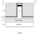
- FIG. 5shows the formation of a gate conductor 20 .
- the gate conductor 20is deposited on the structure of FIG. 4 .
- the gate conductor 20can be a metal (e.g., tungsten, titanium, tantalum, ruthenium, zirconium, cobalt, copper, aluminum, lead, platinum, tin, silver, gold), a conducting metallic compound material (e.g., tantalum nitride, titanium nitride, tungsten silicide, tungsten nitride, titanium nitride, tantalum nitride, ruthenium oxide, cobalt silicide, nickel silicide), conductive carbon, polycrystalline or amorphous silicon, germanium, silicon germanium, or any suitable combination of these materials known to those of skill in the art.
- a metale.g., tungsten, titanium, tantalum, ruthenium, zirconium, cobalt, copper, aluminum, lead, platinum, tin, silver
- the conductive materialmay further comprise dopants that are incorporated during or after deposition.
- the gate conductor 20can be deposited, for example, by atomic layer deposition (ALD), molecular layer deposition (MLD), chemical vapor deposition (CVD), physical vapor deposition, sputtering, plating, evaporation, ion beam deposition, electron beam deposition, laser assisted deposition, and chemical solution deposition, or any suitable combination of those methods.
- ALDatomic layer deposition
- MLDmolecular layer deposition
- CVDchemical vapor deposition
- physical vapor depositionsputtering
- platingevaporation, ion beam deposition
- electron beam depositionelectron beam deposition
- laser assisted depositionlaser assisted deposition
- chemical solution depositionchemical solution deposition
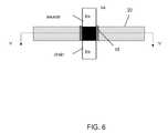
- FIG. 6shows a cross sectional view of the finFET of FIG. 5 , along X-X. Specifically, FIG. 6 shows the source and drain of the finFET, in addition to the structures described herein.
- the resulting integrated circuit chips of each aspect of the inventioncan be distributed by the fabricator in raw wafer form (that is, as a single wafer that has multiple unpackaged chips), as a bare die, or in a packaged form.
- the chipis mounted in a single chip package (e.g., a plastic carrier, with leads that are affixed to a motherboard or other higher level carrier) or in a multichip package (e.g., a ceramic carrier that has either or both surface interconnections or buried interconnections).
- the chipis then integrated with other chips, discrete circuit elements, and/or other signal processing devices as part of either (a) an intermediate product, such as a motherboard, or (b) an end product.
- the end productcan be any product that includes integrated circuit chips, ranging from toys and other low-end applications to advanced computer products having a display, a keyboard or other input device, and a central processor.
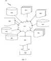
- FIG. 7shows a block diagram of an exemplary design flow 900 used for example, in semiconductor IC logic design, simulation, test, layout, and manufacture.
- Design flow 900includes processes and mechanisms for processing design structures or devices to generate logically or otherwise functionally equivalent representations of the design structures and/or devices described above and shown in FIGS. 5 and 6 .
- the design structures processed and/or generated by design flow 900may be encoded on machine-readable transmission or storage media to include data and/or instructions that when executed or otherwise processed on a data processing system generate a logically, structurally, mechanically, or otherwise functionally equivalent representation of hardware components, circuits, devices, or systems.
- Design flow 900may vary depending on the type of representation being designed.
- a design flow 900 for building an application specific ICmay differ from a design flow 900 for designing a standard component or from a design flow 900 for instantiating the design into a programmable array, for example a programmable gate array (PGA) or a field programmable gate array (FPGA) offered by Altera® Inc. or Xilinx® Inc.
- PGAprogrammable gate array
- FPGAfield programmable gate array
- FIG. 7illustrates multiple such design structures including an input design structure 920 that is preferably processed by a design process 910 .
- Design structure 920may be a logical simulation design structure generated and processed by design process 910 to produce a logically equivalent functional representation of a hardware device.
- Design structure 920may also or alternatively comprise data and/or program instructions that when processed by design process 910 , generate a functional representation of the physical structure of a hardware device. Whether representing functional and/or structural design features, design structure 920 may be generated using electronic computer-aided design (ECAD) such as implemented by a core developer/designer.
- ECADelectronic computer-aided design
- design structure 920When encoded on a machine-readable data transmission, gate array, or storage medium, design structure 920 may be accessed and processed by one or more hardware and/or software modules within design process 910 to simulate or otherwise functionally represent an electronic component, circuit, electronic or logic module, apparatus, device, or system such as those shown in FIGS. 5 and 6 .
- design structure 920may comprise files or other data structures including human and/or machine-readable source code, compiled structures, and computer-executable code structures that when processed by a design or simulation data processing system, functionally simulate or otherwise represent circuits or other levels of hardware logic design.
- Such data structuresmay include hardware-description language (HDL) design entities or other data structures conforming to and/or compatible with lower-level HDL design languages such as Verilog and VHDL, and/or higher level design languages such as C or C++.
- HDLhardware-description language
- Design process 910preferably employs and incorporates hardware and/or software modules for synthesizing, translating, or otherwise processing a design/simulation functional equivalent of the components, circuits, devices, or logic structures shown in FIGS. 5 and 6 to generate a netlist 980 which may contain design structures such as design structure 920 .
- Netlist 980may comprise, for example, compiled or otherwise processed data structures representing a list of wires, discrete components, logic gates, control circuits, I/O devices, models, etc. that describes the connections to other elements and circuits in an integrated circuit design.
- Netlist 980may be synthesized using an iterative process in which netlist 980 is resynthesized one or more times depending on design specifications and parameters for the device.
- netlist 980may be recorded on a machine-readable data storage medium or programmed into a programmable gate array.
- the mediummay be a non-volatile storage medium such as a magnetic or optical disk drive, a programmable gate array, a compact flash, or other flash memory. Additionally, or in the alternative, the medium may be a system or cache memory, buffer space, or electrically or optically conductive devices and materials on which data packets may be transmitted and intermediately stored via the Internet, or other networking suitable means.
- Design process 910may include hardware and software modules for processing a variety of input data structure types including netlist 980 .
- data structure typesmay reside, for example, within library elements 930 and include a set of commonly used elements, circuits, and devices, including models, layouts, and symbolic representations, for a given manufacturing technology (e.g., different technology nodes, 32 nm, 45 nm, 90 nm, etc.).
- the data structure typesmay further include design specifications 940 , characterization data 950 , verification data 960 , design rules 970 , and test data files 985 which may include input test patterns, output test results, and other testing information.
- Design process 910may further include, for example, standard mechanical design processes such as stress analysis, thermal analysis, mechanical event simulation, process simulation for operations such as casting, molding, and die press forming, etc.
- standard mechanical design processessuch as stress analysis, thermal analysis, mechanical event simulation, process simulation for operations such as casting, molding, and die press forming, etc.
- One of ordinary skill in the art of mechanical designcan appreciate the extent of possible mechanical design tools and applications used in design process 910 without deviating from the scope and spirit of the invention.
- Design process 910may also include modules for performing standard circuit design processes such as timing analysis, verification, design rule checking, place and route operations, etc.
- Design process 910employs and incorporates logic and physical design tools such as HDL compilers and simulation model build tools to process design structure 920 together with some or all of the depicted supporting data structures along with any additional mechanical design or data (if applicable), to generate a second design structure 990 .
- Design structure 990resides on a storage medium or programmable gate array in a data format used for the exchange of data of mechanical devices and structures (e.g. information stored in a IGES, DXF, Parasolid XT, JT, DRG, or any other suitable format for storing or rendering such mechanical design structures).
- design structure 990preferably comprises one or more files, data structures, or other computer-encoded data or instructions that reside on transmission or data storage media and that when processed by an ECAD system generate a logically or otherwise functionally equivalent form of one or more of the embodiments of the invention shown in FIGS. 5 and 6 .
- design structure 990may comprise a compiled, executable HDL simulation model that functionally simulates the devices shown in FIGS. 5 and 6 .
- Design structure 990may also employ a data format used for the exchange of layout data of integrated circuits and/or symbolic data format (e.g. information stored in a GDSII (GDS2), GL1, OASIS, map files, or any other suitable format for storing such design data structures).
- Design structure 990may comprise information such as, for example, symbolic data, map files, test data files, design content files, manufacturing data, layout parameters, wires, levels of metal, vias, shapes, data for routing through the manufacturing line, and any other data required by a manufacturer or other designer/developer to produce a device or structure as described above and shown in FIGS. 5 and 6 .
- Design structure 990may then proceed to a stage 995 where, for example, design structure 990 : proceeds to tape-out, is released to manufacturing, is released to a mask house, is sent to another design house, is sent back to the customer, etc.
Landscapes
- Thin Film Transistor (AREA)
Abstract
Description
- The present invention relates to a semiconductor device and a method of manufacturing and, more particularly, to a semiconductor device having an oxygen diffusion barrier layer between a high-k dielectric and a buried oxide layer (BOX).
- Generally, multi-gated non-planar CMOS technology includes metal-oxide semiconductor transistors having a buried oxide layer (BOX) layer formed on a substrate, e.g., a buried oxide layer in a semiconductor-on-insulator substrate. A gate stack, typically of metal and/or polysilicon, is formed on the BOX layer to form the transistor, itself. The gate stack can also include a nitride cap. A high-k dielectric material is blanket deposited on the BOX and the transistor, prior to the deposition of the gate conductor and further processes to complete the transistor.
- The BOX layer, however, is susceptible to oxygen diffusion which can negatively affect the performance of the device. That is, outdiffusing oxygen into the high-k dielectric can have many deleterious affects on the performance of the device. For example, the outdiffusion of oxygen into the high-k dielectric can cause growth of extra oxide at the interface of the high-k dielectric and the semiconductor substrate. This, in turn, can result in an increase in equivalent oxide thickness (EOT) and Vt variation. More specifically, the outdiffusion of oxygen can change the work function of the device and hence cause Vt shift. Also, it is known that oxygen can lower the k-value of the high-k material. This, in turn, can negatively affect the device performance.
- Accordingly, there exists a need in the art to overcome the deficiencies and limitations described hereinabove.
- In a first aspect of the invention, a method comprises depositing a diffusion barrier layer on a BOX layer and gate structure and etching a portion of the diffusion barrier layer from sidewalls of the gate structure. The method further comprises depositing a high-k dielectric on the diffusion barrier layer and the gate structure.
- In another aspect of the invention, a structure comprises a BOX provided on a substrate and a gate structure formed on the BOX. A diffusion barrier film is deposited on the BOX and a high-k material is formed on the diffusion barrier film. The diffusion barrier film contacts sidewalls of the gate structure.
- In a further aspect of the invention, a design structure is embodied in a machine readable medium for designing, manufacturing, or testing an integrated circuit. The design structure comprises: gate structure formed on a BOX; a nitride diffusion barrier film deposited on the BOX; and a high-k dielectric material formed on the nitride diffusion barrier film and contacting sidewalls of the gate structure.
- The present invention is described in the detailed description which follows, in reference to the noted plurality of drawings by way of non-limiting examples of exemplary embodiments of the present invention.
FIGS. 1-4 show intermediate structures and respective processing steps in accordance with aspects of the invention;FIG. 5 shows a final structure and respective processing steps according to the aspects of the invention;FIG. 6 shows a cross sectional view of a finFET ofFIG. 5 according to the aspects of the invention; andFIG. 7 is a flow diagram of a design process used in semiconductor design, manufacture, and/or test.- The present invention relates to a semiconductor device and a method of manufacturing and, more particularly, to a semiconductor device having an oxygen diffusion barrier layer. Advantageously, the present invention prevents outdiffusion of oxygen from an underlying BOX layer to increase device performance. More specifically, the present invention provides a nitride barrier layer between a BOX and a high-k dielectric to prevent oxygen from diffusing into the high-k material which, in turn, can decrease the k value of the dielectric, increase an equivalent oxide thickness (EOT) of the device, and change the work function of the device by shifting Vt, e.g., increasing Vt. The devices manufactured using the processes of the present invention will benefit from such advantages.
FIGS. 1-4 show intermediate structures and respective processing steps in accordance with the invention. In particular,FIG. 1 shows a BOX (buried oxide layer)12 formed over an underlying substrate10 using conventional deposition, bonding, and/or separation by implantation of oxygen (SIMOX) processes known to those of skill in the art. TheBOX 12 may be a buried oxide layer in a semiconductor-on-insulator (SOI) substrate or an oxide in a trench isolation. In embodiments, theBOX 12 may be about 100 Å to 3000 Å in thickness; although this range of thickness should not be considered a limiting factor as other dimensions are also contemplated by the present invention. The substrate10 can be a bulk semiconductor (e.g., silicon) or a portion of a semiconductor substrate which has a thickness of about 700 microns to 750 microns, as one example. It should be understood by those of skill in the art that the substrate can also vary in thickness depending on particular design applications.- Still referring to
FIG. 1 , agate structure 14 is formed abutting theBOX 12 in a conventional manner. In one embodiment, thegate structure 14 is designed for use as a finFET. Thegate structure 14 includes asemiconductor body 14aand anitride cap 14b, formed through a conventional lithography and etching process such that further explanation is not required herein for a person of ordinary skill in the art to practice the invention. In alternate embodiments, thegate structure 14 can be formed using spacer image transfer techniques. Thesemiconductor body 14acan comprise any semiconductor material, including but not limited to silicon, germanium, silicon germanium, silicon carbide, III-V compound semiconductors (e.g., GaAs), II-VI compound semiconductors. A portion or entire portion of thesemiconductor body 14amay be amorphous, polycrystalline, or monocrystalline. Thesemiconductor body 14amay be doped, undoped or contain doped regions and undoped regions therein. Thesemiconductor body 14amay contain regions with strain and regions without strain therein, or contain regions of tensile strain and compressive strain. In one embodiment, thebody 14ais made of a silicon layer on an SOI (semiconductor-on-insulator) substrate, and can range in thickness from about 100 Å to 1000 Å and preferably 200 Å to 400 Å; although other dimensions are contemplated by the invention. Thenitride cap 14bcan range in thickness from about 100 Å to 500 Å, and preferably from about 200 Å to 300 Å. - In
FIG. 2 , a nitride deposition process is performed to deposit anitride film 16 on the structure ofFIG. 1 . More specifically, in embodiments, an anisotropic nitride deposition using, for example, high density plasma (HDP) techniques is used to form thenitride film 16. In embodiments, using an anisotropic nitride deposition, thenitride film 16 on the planar surface is thicker than that of the sidewall (e.g., vertical or substantially vertical) surfaces, e.g., t2>t1. In embodiments, t1 can range from about 20 Å to 50 Å, with t2 about two to three times greater than t1. In one non-limiting example, t1 is about 30 Å and t2 is about 80 Å. In embodiments, thenitride film 16 is a diffusion barrier film which is designed to block oxygen diffusion from theBOX 12 into a high-k gate dielectric which will be formed later. Optionally, a thermal oxidation process is performed to form anoxide liner 13 on the sidewall of theSOI body 14abefore HDP nitride deposition. Theoxide liner 13, when present, prevents damage on theSOI body 14aduring the subsequent processes. For example, theoxide liner 13 prevents plasma damage on the surface of theSOI body 14aduring the deposition ofHDP nitride film 16. Theoxide liner 13 is omitted in subsequent figures for simplicity. FIG. 3 shows an etch back process in accordance with the invention. In this implementation, the nitride sidewall on thegate structure 14 is removed using a conventional etching process, for example, a wet etch process with an etch solution containing hydrofluoric/ethylene glycol (HF/EG) or hot phosphoric acid (H3PO4). Alternatively, dry etch such as plasma downstream etch (CDE) can be used to etch thenitride film 16. This etching process also removes a portion of thenitride film 16 on the planar surface. Theoxide liner 13, if present and not removed during the etch back process, can be removed from the sidewall of thesemiconductor body 14aat this stage by a conventional etching process, for example, a wet etch process with a solution containing hydrofluoric acid (HF).- In a specific, non-limiting example, t1 is about 30 Å and t2 is about 80 Å. In this example, a 40 Å timed nitride etch is used to remove the 30 Å nitride film on the sidewalls of the
gate structure 14. This process leaves about a 40 Å thick nitride film on the planar surfaces (e.g., on theBOX 12 andcap 14b). In embodiments, the 40Å nitride film 16 is sufficient to block oxygen diffusion from theBOX 12 into a high-k gate dielectric. - In
FIG. 4 , a high-k dielectric 18 is deposited on the structure ofFIG. 4 . In embodiments, the high-k dielectric 18 is deposited over thenitride film 16, which prevents oxygen out-diffusing from theBOX 12. In embodiments, the high-k dielectric can be deposited using a conventional chemical vapor deposition (CVD) process, an atomic layer deposition (ALD) process, molecular layer deposition (MLD), rapid thermal chemical vapor deposition (RTCVD), in-situ radical assisted deposition, ultrahigh vacuum chemical vapor deposition (UHVCVD), metallorganic chemical vapor deposition (MOCVD), physical vapor deposition, electron beam deposition, laser assisted deposition, and/or chemical solution deposition. Examples of the high-k dielectric 18 include but are not limited to metal oxides such as hafnium oxide, hafnium silicon oxide, hafnium silicon oxynitride, lanthanum oxide, lanthanum aluminum oxide, zirconium oxide, zirconium silicon oxide, zirconium silicon oxynitride, tantalum oxide, titanium oxide, barium strontium titanium oxide, barium titanium oxide, strontium titanium oxide, yttrium oxide, aluminum oxide, lead scandium tantalum oxide, and lead zinc niobate, an any combination of these materials. The high-k dielectric 18 can be deposited in the range of about 15 Å to 100 Å and typically in the range of about 15 Å to 30 Å; although, other dimensions are also contemplated by the invention. Optionally, an interfacial layer (not shown) such as silicon oxide, silicon nitride, or silicon oxynitride can be formed on the exposed surface of theSOI body 14abefore deposition of the high-k dielectric 18. The interfacial layer can be formed by thermal oxidation, thermal nitridation, plasma oxidation, plasma nitridation, chemical oxidation, or any combination of those methods. FIG. 5 shows the formation of agate conductor 20. In embodiments, thegate conductor 20 is deposited on the structure ofFIG. 4 . Thegate conductor 20 can be a metal (e.g., tungsten, titanium, tantalum, ruthenium, zirconium, cobalt, copper, aluminum, lead, platinum, tin, silver, gold), a conducting metallic compound material (e.g., tantalum nitride, titanium nitride, tungsten silicide, tungsten nitride, titanium nitride, tantalum nitride, ruthenium oxide, cobalt silicide, nickel silicide), conductive carbon, polycrystalline or amorphous silicon, germanium, silicon germanium, or any suitable combination of these materials known to those of skill in the art. The conductive material may further comprise dopants that are incorporated during or after deposition. Thegate conductor 20 can be deposited, for example, by atomic layer deposition (ALD), molecular layer deposition (MLD), chemical vapor deposition (CVD), physical vapor deposition, sputtering, plating, evaporation, ion beam deposition, electron beam deposition, laser assisted deposition, and chemical solution deposition, or any suitable combination of those methods. In embodiments, after deposition, thegate conductor 20 is planarized using conventional processes, for example, chemically mechanical polishing (CMP). Conventional processes are performed after the deposition of thegate conductor 20 to complete finFET formation, which do not require further explanation to those of skill in the art.FIG. 6 shows a cross sectional view of the finFET ofFIG. 5 , along X-X. Specifically,FIG. 6 shows the source and drain of the finFET, in addition to the structures described herein.- The resulting integrated circuit chips of each aspect of the invention can be distributed by the fabricator in raw wafer form (that is, as a single wafer that has multiple unpackaged chips), as a bare die, or in a packaged form. In the latter case, the chip is mounted in a single chip package (e.g., a plastic carrier, with leads that are affixed to a motherboard or other higher level carrier) or in a multichip package (e.g., a ceramic carrier that has either or both surface interconnections or buried interconnections). In any case the chip is then integrated with other chips, discrete circuit elements, and/or other signal processing devices as part of either (a) an intermediate product, such as a motherboard, or (b) an end product. The end product can be any product that includes integrated circuit chips, ranging from toys and other low-end applications to advanced computer products having a display, a keyboard or other input device, and a central processor.
FIG. 7 shows a block diagram of anexemplary design flow 900 used for example, in semiconductor IC logic design, simulation, test, layout, and manufacture.Design flow 900 includes processes and mechanisms for processing design structures or devices to generate logically or otherwise functionally equivalent representations of the design structures and/or devices described above and shown inFIGS. 5 and 6 . The design structures processed and/or generated bydesign flow 900 may be encoded on machine-readable transmission or storage media to include data and/or instructions that when executed or otherwise processed on a data processing system generate a logically, structurally, mechanically, or otherwise functionally equivalent representation of hardware components, circuits, devices, or systems.Design flow 900 may vary depending on the type of representation being designed. For example, adesign flow 900 for building an application specific IC (ASIC) may differ from adesign flow 900 for designing a standard component or from adesign flow 900 for instantiating the design into a programmable array, for example a programmable gate array (PGA) or a field programmable gate array (FPGA) offered by Altera® Inc. or Xilinx® Inc.FIG. 7 illustrates multiple such design structures including aninput design structure 920 that is preferably processed by adesign process 910.Design structure 920 may be a logical simulation design structure generated and processed bydesign process 910 to produce a logically equivalent functional representation of a hardware device.Design structure 920 may also or alternatively comprise data and/or program instructions that when processed bydesign process 910, generate a functional representation of the physical structure of a hardware device. Whether representing functional and/or structural design features,design structure 920 may be generated using electronic computer-aided design (ECAD) such as implemented by a core developer/designer. When encoded on a machine-readable data transmission, gate array, or storage medium,design structure 920 may be accessed and processed by one or more hardware and/or software modules withindesign process 910 to simulate or otherwise functionally represent an electronic component, circuit, electronic or logic module, apparatus, device, or system such as those shown inFIGS. 5 and 6 . As such,design structure 920 may comprise files or other data structures including human and/or machine-readable source code, compiled structures, and computer-executable code structures that when processed by a design or simulation data processing system, functionally simulate or otherwise represent circuits or other levels of hardware logic design. Such data structures may include hardware-description language (HDL) design entities or other data structures conforming to and/or compatible with lower-level HDL design languages such as Verilog and VHDL, and/or higher level design languages such as C or C++.Design process 910 preferably employs and incorporates hardware and/or software modules for synthesizing, translating, or otherwise processing a design/simulation functional equivalent of the components, circuits, devices, or logic structures shown inFIGS. 5 and 6 to generate anetlist 980 which may contain design structures such asdesign structure 920.Netlist 980 may comprise, for example, compiled or otherwise processed data structures representing a list of wires, discrete components, logic gates, control circuits, I/O devices, models, etc. that describes the connections to other elements and circuits in an integrated circuit design.Netlist 980 may be synthesized using an iterative process in which netlist980 is resynthesized one or more times depending on design specifications and parameters for the device. As with other design structure types described herein,netlist 980 may be recorded on a machine-readable data storage medium or programmed into a programmable gate array. The medium may be a non-volatile storage medium such as a magnetic or optical disk drive, a programmable gate array, a compact flash, or other flash memory. Additionally, or in the alternative, the medium may be a system or cache memory, buffer space, or electrically or optically conductive devices and materials on which data packets may be transmitted and intermediately stored via the Internet, or other networking suitable means.Design process 910 may include hardware and software modules for processing a variety of input data structuretypes including netlist 980. Such data structure types may reside, for example, withinlibrary elements 930 and include a set of commonly used elements, circuits, and devices, including models, layouts, and symbolic representations, for a given manufacturing technology (e.g., different technology nodes, 32 nm, 45 nm, 90 nm, etc.). The data structure types may further includedesign specifications 940,characterization data 950,verification data 960,design rules 970, and test data files985 which may include input test patterns, output test results, and other testing information.Design process 910 may further include, for example, standard mechanical design processes such as stress analysis, thermal analysis, mechanical event simulation, process simulation for operations such as casting, molding, and die press forming, etc. One of ordinary skill in the art of mechanical design can appreciate the extent of possible mechanical design tools and applications used indesign process 910 without deviating from the scope and spirit of the invention.Design process 910 may also include modules for performing standard circuit design processes such as timing analysis, verification, design rule checking, place and route operations, etc.Design process 910 employs and incorporates logic and physical design tools such as HDL compilers and simulation model build tools to processdesign structure 920 together with some or all of the depicted supporting data structures along with any additional mechanical design or data (if applicable), to generate asecond design structure 990.Design structure 990 resides on a storage medium or programmable gate array in a data format used for the exchange of data of mechanical devices and structures (e.g. information stored in a IGES, DXF, Parasolid XT, JT, DRG, or any other suitable format for storing or rendering such mechanical design structures). Similar to designstructure 920,design structure 990 preferably comprises one or more files, data structures, or other computer-encoded data or instructions that reside on transmission or data storage media and that when processed by an ECAD system generate a logically or otherwise functionally equivalent form of one or more of the embodiments of the invention shown inFIGS. 5 and 6 . In one embodiment,design structure 990 may comprise a compiled, executable HDL simulation model that functionally simulates the devices shown inFIGS. 5 and 6 .Design structure 990 may also employ a data format used for the exchange of layout data of integrated circuits and/or symbolic data format (e.g. information stored in a GDSII (GDS2), GL1, OASIS, map files, or any other suitable format for storing such design data structures).Design structure 990 may comprise information such as, for example, symbolic data, map files, test data files, design content files, manufacturing data, layout parameters, wires, levels of metal, vias, shapes, data for routing through the manufacturing line, and any other data required by a manufacturer or other designer/developer to produce a device or structure as described above and shown inFIGS. 5 and 6 .Design structure 990 may then proceed to astage 995 where, for example, design structure990: proceeds to tape-out, is released to manufacturing, is released to a mask house, is sent to another design house, is sent back to the customer, etc.- The terminology used herein is for the purpose of describing particular embodiments only and is not intended to be limiting of the invention. As used herein, the singular forms “a”, “an” and “the” are intended to include the plural forms as well, unless the context clearly indicates otherwise. It will be further understood that the terms “comprises” and/or “comprising,” when used in this specification, specify the presence of stated features, integers, steps, operations, elements, and/or components, but do not preclude the presence or addition of one or more other features, integers, steps, operations, elements, components, and/or groups thereof.
- The corresponding structures, materials, acts, and equivalents of all means or step plus function elements, if any, in the claims below are intended to include any structure, material, or act for performing the function in combination with other claimed elements as specifically claimed. The description of the present invention has been presented for purposes of illustration and description, but is not intended to be exhaustive or limited to the invention in the form disclosed. Many modifications and variations will be apparent to those of ordinary skill in the art without departing from the scope and spirit of the invention. The embodiments were chosen and described in order to best explain the principles of the invention and the practical application, and to enable others of ordinary skill in the art to understand the invention for various embodiments with various modifications as are suited to the particular use contemplated.
Claims (20)
Priority Applications (1)
| Application Number | Priority Date | Filing Date | Title |
|---|---|---|---|
| US12/178,303US7833891B2 (en) | 2008-07-23 | 2008-07-23 | Semiconductor device manufacturing method using oxygen diffusion barrier layer between buried oxide layer and high K dielectric layer |
Applications Claiming Priority (1)
| Application Number | Priority Date | Filing Date | Title |
|---|---|---|---|
| US12/178,303US7833891B2 (en) | 2008-07-23 | 2008-07-23 | Semiconductor device manufacturing method using oxygen diffusion barrier layer between buried oxide layer and high K dielectric layer |
Publications (2)
| Publication Number | Publication Date |
|---|---|
| US20100019358A1true US20100019358A1 (en) | 2010-01-28 |
| US7833891B2 US7833891B2 (en) | 2010-11-16 |
Family
ID=41567888
Family Applications (1)
| Application Number | Title | Priority Date | Filing Date |
|---|---|---|---|
| US12/178,303Expired - Fee RelatedUS7833891B2 (en) | 2008-07-23 | 2008-07-23 | Semiconductor device manufacturing method using oxygen diffusion barrier layer between buried oxide layer and high K dielectric layer |
Country Status (1)
| Country | Link |
|---|---|
| US (1) | US7833891B2 (en) |
Cited By (6)
| Publication number | Priority date | Publication date | Assignee | Title |
|---|---|---|---|---|
| US20120280235A1 (en)* | 2011-05-03 | 2012-11-08 | Boe Technology Group Co., Ltd. | Thin film fet device and method for forming the same |
| US8492247B2 (en) | 2010-08-17 | 2013-07-23 | International Business Machines Corporation | Programmable FETs using Vt-shift effect and methods of manufacture |
| US20180350969A1 (en)* | 2017-05-30 | 2018-12-06 | Taiwan Semiconductor Manufacturing Co., Ltd. | Semiconductor device structure and method of forming the same |
| CN115036312A (en)* | 2021-03-04 | 2022-09-09 | 华邦电子股份有限公司 | Semiconductor memory structure and method of forming the same |
| US20220352175A1 (en)* | 2021-04-28 | 2022-11-03 | Changxin Memory Technologies, Inc. | Method of manufacturing semiconductor structure |
| US20220367475A1 (en)* | 2021-05-14 | 2022-11-17 | Winbond Electronics Corp. | Semiconductor memory structure and method for manufacturing the same |
Families Citing this family (2)
| Publication number | Priority date | Publication date | Assignee | Title |
|---|---|---|---|---|
| JP4963021B2 (en)* | 2005-09-06 | 2012-06-27 | 独立行政法人産業技術総合研究所 | Semiconductor structure |
| FR2972564B1 (en)* | 2011-03-08 | 2016-11-04 | S O I Tec Silicon On Insulator Tech | METHOD FOR PROCESSING A SEMICONDUCTOR TYPE STRUCTURE ON INSULATION |
Citations (28)
| Publication number | Priority date | Publication date | Assignee | Title |
|---|---|---|---|---|
| US5436186A (en)* | 1994-04-22 | 1995-07-25 | United Microelectronics Corporation | Process for fabricating a stacked capacitor |
| US5457065A (en)* | 1994-12-14 | 1995-10-10 | United Microelectronics Corporation | method of manufacturing a new DRAM capacitor structure having increased capacitance |
| US5460999A (en)* | 1994-06-06 | 1995-10-24 | United Microelectronics Corporation | Method for making fin-shaped stack capacitors on DRAM chips |
| US20010041250A1 (en)* | 2000-03-07 | 2001-11-15 | Werkhoven Christian J. | Graded thin films |
| US6403434B1 (en)* | 2001-02-09 | 2002-06-11 | Advanced Micro Devices, Inc. | Process for manufacturing MOS transistors having elevated source and drain regions and a high-k gate dielectric |
| US20020115252A1 (en)* | 2000-10-10 | 2002-08-22 | Haukka Suvi P. | Dielectric interface films and methods therefor |
| US6495437B1 (en)* | 2001-02-09 | 2002-12-17 | Advanced Micro Devices, Inc. | Low temperature process to locally form high-k gate dielectrics |
| US6524920B1 (en)* | 2001-02-09 | 2003-02-25 | Advanced Micro Devices, Inc. | Low temperature process for a transistor with elevated source and drain |
| US6551885B1 (en)* | 2001-02-09 | 2003-04-22 | Advanced Micro Devices, Inc. | Low temperature process for a thin film transistor |
| US6756277B1 (en)* | 2001-02-09 | 2004-06-29 | Advanced Micro Devices, Inc. | Replacement gate process for transistors having elevated source and drain regions |
| US6787424B1 (en)* | 2001-02-09 | 2004-09-07 | Advanced Micro Devices, Inc. | Fully depleted SOI transistor with elevated source and drain |
| US20050142738A1 (en)* | 2003-12-30 | 2005-06-30 | Lee Byeong R. | Method of fabricating a fin field effect transistor |
| US20060043421A1 (en)* | 2004-09-01 | 2006-03-02 | International Business Machines Corporation | Multi-gate device with high k dielectric for channel top surface |
| US7061360B2 (en)* | 2001-06-15 | 2006-06-13 | E2V Technologies (Uk) Limited | Transformer/rectifier arrangement |
| US7071122B2 (en)* | 2003-12-10 | 2006-07-04 | International Business Machines Corporation | Field effect transistor with etched-back gate dielectric |
| US7105390B2 (en)* | 2003-12-30 | 2006-09-12 | Intel Corporation | Nonplanar transistors with metal gate electrodes |
| US7176483B2 (en)* | 2002-08-12 | 2007-02-13 | Acorn Technologies, Inc. | Method for depinning the Fermi level of a semiconductor at an electrical junction and devices incorporating such junctions |
| US7193279B2 (en)* | 2005-01-18 | 2007-03-20 | Intel Corporation | Non-planar MOS structure with a strained channel region |
| US7241674B2 (en)* | 2004-05-13 | 2007-07-10 | Taiwan Semiconductor Manufacturing Co., Ltd. | Method of forming silicided gate structure |
| US7241653B2 (en)* | 2003-06-27 | 2007-07-10 | Intel Corporation | Nonplanar device with stress incorporation layer and method of fabrication |
| US7268058B2 (en)* | 2004-01-16 | 2007-09-11 | Intel Corporation | Tri-gate transistors and methods to fabricate same |
| US7279375B2 (en)* | 2005-06-30 | 2007-10-09 | Intel Corporation | Block contact architectures for nanoscale channel transistors |
| US7304336B2 (en)* | 2003-02-13 | 2007-12-04 | Massachusetts Institute Of Technology | FinFET structure and method to make the same |
| US7326656B2 (en)* | 2004-09-30 | 2008-02-05 | Intel Corporation | Method of forming a metal oxide dielectric |
| US7326634B2 (en)* | 2004-03-31 | 2008-02-05 | Intel Corporation | Bulk non-planar transistor having strained enhanced mobility and methods of fabrication |
| US7348284B2 (en)* | 2004-08-10 | 2008-03-25 | Intel Corporation | Non-planar pMOS structure with a strained channel region and an integrated strained CMOS flow |
| US7358121B2 (en)* | 2002-08-23 | 2008-04-15 | Intel Corporation | Tri-gate devices and methods of fabrication |
| US20090039426A1 (en)* | 2007-08-10 | 2009-02-12 | International Business Machines Corporation | Extremely-thin silicon-on-insulator transistor with raised source/drain |
- 2008
- 2008-07-23USUS12/178,303patent/US7833891B2/ennot_activeExpired - Fee Related
Patent Citations (36)
| Publication number | Priority date | Publication date | Assignee | Title |
|---|---|---|---|---|
| US5436186A (en)* | 1994-04-22 | 1995-07-25 | United Microelectronics Corporation | Process for fabricating a stacked capacitor |
| US5716884A (en)* | 1994-04-22 | 1998-02-10 | United Microelectronics Corporation | Process for fabricating a stacked capacitor |
| US5460999A (en)* | 1994-06-06 | 1995-10-24 | United Microelectronics Corporation | Method for making fin-shaped stack capacitors on DRAM chips |
| US5457065A (en)* | 1994-12-14 | 1995-10-10 | United Microelectronics Corporation | method of manufacturing a new DRAM capacitor structure having increased capacitance |
| US6703708B2 (en)* | 2000-03-07 | 2004-03-09 | Asm International N.V. | Graded thin films |
| US6534395B2 (en)* | 2000-03-07 | 2003-03-18 | Asm Microchemistry Oy | Method of forming graded thin films using alternating pulses of vapor phase reactants |
| US6933225B2 (en)* | 2000-03-07 | 2005-08-23 | Asm International N.V. | Graded thin films |
| US20010041250A1 (en)* | 2000-03-07 | 2001-11-15 | Werkhoven Christian J. | Graded thin films |
| US20020115252A1 (en)* | 2000-10-10 | 2002-08-22 | Haukka Suvi P. | Dielectric interface films and methods therefor |
| US6660660B2 (en)* | 2000-10-10 | 2003-12-09 | Asm International, Nv. | Methods for making a dielectric stack in an integrated circuit |
| US6403434B1 (en)* | 2001-02-09 | 2002-06-11 | Advanced Micro Devices, Inc. | Process for manufacturing MOS transistors having elevated source and drain regions and a high-k gate dielectric |
| US6495437B1 (en)* | 2001-02-09 | 2002-12-17 | Advanced Micro Devices, Inc. | Low temperature process to locally form high-k gate dielectrics |
| US6524920B1 (en)* | 2001-02-09 | 2003-02-25 | Advanced Micro Devices, Inc. | Low temperature process for a transistor with elevated source and drain |
| US6551885B1 (en)* | 2001-02-09 | 2003-04-22 | Advanced Micro Devices, Inc. | Low temperature process for a thin film transistor |
| US6756277B1 (en)* | 2001-02-09 | 2004-06-29 | Advanced Micro Devices, Inc. | Replacement gate process for transistors having elevated source and drain regions |
| US6787424B1 (en)* | 2001-02-09 | 2004-09-07 | Advanced Micro Devices, Inc. | Fully depleted SOI transistor with elevated source and drain |
| US7061360B2 (en)* | 2001-06-15 | 2006-06-13 | E2V Technologies (Uk) Limited | Transformer/rectifier arrangement |
| US7176483B2 (en)* | 2002-08-12 | 2007-02-13 | Acorn Technologies, Inc. | Method for depinning the Fermi level of a semiconductor at an electrical junction and devices incorporating such junctions |
| US7358121B2 (en)* | 2002-08-23 | 2008-04-15 | Intel Corporation | Tri-gate devices and methods of fabrication |
| US7304336B2 (en)* | 2003-02-13 | 2007-12-04 | Massachusetts Institute Of Technology | FinFET structure and method to make the same |
| US7241653B2 (en)* | 2003-06-27 | 2007-07-10 | Intel Corporation | Nonplanar device with stress incorporation layer and method of fabrication |
| US7071122B2 (en)* | 2003-12-10 | 2006-07-04 | International Business Machines Corporation | Field effect transistor with etched-back gate dielectric |
| US20050142738A1 (en)* | 2003-12-30 | 2005-06-30 | Lee Byeong R. | Method of fabricating a fin field effect transistor |
| US7105390B2 (en)* | 2003-12-30 | 2006-09-12 | Intel Corporation | Nonplanar transistors with metal gate electrodes |
| US7329913B2 (en)* | 2003-12-30 | 2008-02-12 | Intel Corporation | Nonplanar transistors with metal gate electrodes |
| US7268058B2 (en)* | 2004-01-16 | 2007-09-11 | Intel Corporation | Tri-gate transistors and methods to fabricate same |
| US7326634B2 (en)* | 2004-03-31 | 2008-02-05 | Intel Corporation | Bulk non-planar transistor having strained enhanced mobility and methods of fabrication |
| US7241674B2 (en)* | 2004-05-13 | 2007-07-10 | Taiwan Semiconductor Manufacturing Co., Ltd. | Method of forming silicided gate structure |
| US7348284B2 (en)* | 2004-08-10 | 2008-03-25 | Intel Corporation | Non-planar pMOS structure with a strained channel region and an integrated strained CMOS flow |
| US20060043421A1 (en)* | 2004-09-01 | 2006-03-02 | International Business Machines Corporation | Multi-gate device with high k dielectric for channel top surface |
| US20080070366A1 (en)* | 2004-09-01 | 2008-03-20 | International Business Machines Corporation | Multi-gate device with high k dielectric for channel top surface |
| US7326656B2 (en)* | 2004-09-30 | 2008-02-05 | Intel Corporation | Method of forming a metal oxide dielectric |
| US7361958B2 (en)* | 2004-09-30 | 2008-04-22 | Intel Corporation | Nonplanar transistors with metal gate electrodes |
| US7193279B2 (en)* | 2005-01-18 | 2007-03-20 | Intel Corporation | Non-planar MOS structure with a strained channel region |
| US7279375B2 (en)* | 2005-06-30 | 2007-10-09 | Intel Corporation | Block contact architectures for nanoscale channel transistors |
| US20090039426A1 (en)* | 2007-08-10 | 2009-02-12 | International Business Machines Corporation | Extremely-thin silicon-on-insulator transistor with raised source/drain |
Cited By (16)
| Publication number | Priority date | Publication date | Assignee | Title |
|---|---|---|---|---|
| US8492247B2 (en) | 2010-08-17 | 2013-07-23 | International Business Machines Corporation | Programmable FETs using Vt-shift effect and methods of manufacture |
| CN103503150A (en)* | 2010-08-17 | 2014-01-08 | 国际商业机器公司 | Programmable FET using Vt shift effect and its manufacturing method |
| WO2012024037A3 (en)* | 2010-08-17 | 2014-03-20 | International Business Machines Corporation | PROGRAMMABLE FETs USING Vt-SHIFT EFFECT AND METHODS OF MANUFACTURE |
| US8766378B2 (en) | 2010-08-17 | 2014-07-01 | International Business Machines Corporation | Programmable FETs using Vt-shift effect and methods of manufacture |
| CN103503150B (en)* | 2010-08-17 | 2016-08-03 | 国际商业机器公司 | Programmable FET using Vt shift effect and its manufacturing method |
| US20120280235A1 (en)* | 2011-05-03 | 2012-11-08 | Boe Technology Group Co., Ltd. | Thin film fet device and method for forming the same |
| US10985277B2 (en)* | 2017-05-30 | 2021-04-20 | Taiwan Semiconductor Manufacturing Co., Ltd. | Method for forming semiconductor device structure |
| US10636910B2 (en)* | 2017-05-30 | 2020-04-28 | Taiwan Semiconductor Manufacturing Co., Ltd. | Semiconductor device structure and method of forming the same |
| US20180350969A1 (en)* | 2017-05-30 | 2018-12-06 | Taiwan Semiconductor Manufacturing Co., Ltd. | Semiconductor device structure and method of forming the same |
| US20210234036A1 (en)* | 2017-05-30 | 2021-07-29 | Taiwan Semiconductor Manufacturing Co., Ltd. | Semiconductor device structure |
| US11688809B2 (en)* | 2017-05-30 | 2023-06-27 | Taiwan Semiconductor Manufacturing Co., Ltd. | Semiconductor device structure |
| US12057507B2 (en) | 2017-05-30 | 2024-08-06 | Taiwan Semiconductor Manufacturing Co., Ltd. | Method for manufacturing semiconductor device structure |
| CN115036312A (en)* | 2021-03-04 | 2022-09-09 | 华邦电子股份有限公司 | Semiconductor memory structure and method of forming the same |
| US20220352175A1 (en)* | 2021-04-28 | 2022-11-03 | Changxin Memory Technologies, Inc. | Method of manufacturing semiconductor structure |
| US20220367475A1 (en)* | 2021-05-14 | 2022-11-17 | Winbond Electronics Corp. | Semiconductor memory structure and method for manufacturing the same |
| US11700724B2 (en)* | 2021-05-14 | 2023-07-11 | Winbond Electronics Corp. | Semiconductor memory structure and method for manufacturing the same |
Also Published As
| Publication number | Publication date |
|---|---|
| US7833891B2 (en) | 2010-11-16 |
Similar Documents
| Publication | Publication Date | Title |
|---|---|---|
| US9583628B2 (en) | Semiconductor device with a low-K spacer and method of forming the same | |
| US8420476B2 (en) | Integrated circuit with finFETs and MIM fin capacitor | |
| US7833891B2 (en) | Semiconductor device manufacturing method using oxygen diffusion barrier layer between buried oxide layer and high K dielectric layer | |
| US10580686B2 (en) | Semiconductor structure with integrated passive structures | |
| US8937345B2 (en) | Integrated circuits comprising an active transistor electrically connected to a trench capacitor by an overlying contact | |
| US10361207B2 (en) | Semiconductor structures with deep trench capacitor and methods of manufacture | |
| US8003463B2 (en) | Structure, design structure and method of manufacturing dual metal gate Vt roll-up structure | |
| US9171844B2 (en) | Gate structures and methods of manufacture | |
| US8941190B2 (en) | Semiconductor structures and methods of manufacture | |
| US9214561B2 (en) | Thin body switch transistor | |
| US9153669B2 (en) | Low capacitance finFET gate structure |
Legal Events
| Date | Code | Title | Description |
|---|---|---|---|
| AS | Assignment | Owner name:INTERNATIONAL BUSINESS MACHINES CORPORATION, NEW Y Free format text:ASSIGNMENT OF ASSIGNORS INTEREST;ASSIGNORS:CHENG, KANGGUO;DORIS, BRUCE B.;REEL/FRAME:021357/0365 Effective date:20080711 | |
| REMI | Maintenance fee reminder mailed | ||
| FPAY | Fee payment | Year of fee payment:4 | |
| SULP | Surcharge for late payment | ||
| AS | Assignment | Owner name:GLOBALFOUNDRIES U.S. 2 LLC, NEW YORK Free format text:ASSIGNMENT OF ASSIGNORS INTEREST;ASSIGNOR:INTERNATIONAL BUSINESS MACHINES CORPORATION;REEL/FRAME:036550/0001 Effective date:20150629 | |
| AS | Assignment | Owner name:GLOBALFOUNDRIES INC., CAYMAN ISLANDS Free format text:ASSIGNMENT OF ASSIGNORS INTEREST;ASSIGNORS:GLOBALFOUNDRIES U.S. 2 LLC;GLOBALFOUNDRIES U.S. INC.;REEL/FRAME:036779/0001 Effective date:20150910 | |
| FEPP | Fee payment procedure | Free format text:MAINTENANCE FEE REMINDER MAILED (ORIGINAL EVENT CODE: REM.) | |
| AS | Assignment | Owner name:WILMINGTON TRUST, NATIONAL ASSOCIATION, DELAWARE Free format text:SECURITY AGREEMENT;ASSIGNOR:GLOBALFOUNDRIES INC.;REEL/FRAME:049490/0001 Effective date:20181127 | |
| LAPS | Lapse for failure to pay maintenance fees | Free format text:PATENT EXPIRED FOR FAILURE TO PAY MAINTENANCE FEES (ORIGINAL EVENT CODE: EXP.); ENTITY STATUS OF PATENT OWNER: LARGE ENTITY | |
| STCH | Information on status: patent discontinuation | Free format text:PATENT EXPIRED DUE TO NONPAYMENT OF MAINTENANCE FEES UNDER 37 CFR 1.362 | |
| FP | Lapsed due to failure to pay maintenance fee | Effective date:20181116 | |
| AS | Assignment | Owner name:GLOBALFOUNDRIES INC., CAYMAN ISLANDS Free format text:RELEASE BY SECURED PARTY;ASSIGNOR:WILMINGTON TRUST, NATIONAL ASSOCIATION;REEL/FRAME:054636/0001 Effective date:20201117 | |
| AS | Assignment | Owner name:GLOBALFOUNDRIES U.S. INC., NEW YORK Free format text:RELEASE BY SECURED PARTY;ASSIGNOR:WILMINGTON TRUST, NATIONAL ASSOCIATION;REEL/FRAME:056987/0001 Effective date:20201117 |