US20090324971A1 - Method and apparatus for atomic layer deposition using an atmospheric pressure glow discharge plasma - Google Patents
Method and apparatus for atomic layer deposition using an atmospheric pressure glow discharge plasmaDownload PDFInfo
- Publication number
- US20090324971A1 US20090324971A1US12/304,614US30461407AUS2009324971A1US 20090324971 A1US20090324971 A1US 20090324971A1US 30461407 AUS30461407 AUS 30461407AUS 2009324971 A1US2009324971 A1US 2009324971A1
- Authority
- US
- United States
- Prior art keywords
- substrate
- inert gas
- gas mixture
- precursor
- plasma
- Prior art date
- Legal status (The legal status is an assumption and is not a legal conclusion. Google has not performed a legal analysis and makes no representation as to the accuracy of the status listed.)
- Abandoned
Links
- 238000000034methodMethods0.000titleclaimsabstractdescription89
- 238000000231atomic layer depositionMethods0.000titleclaimsabstractdescription52
- 239000000758substrateSubstances0.000claimsabstractdescription157
- 239000000203mixtureSubstances0.000claimsabstractdescription135
- 239000002243precursorSubstances0.000claimsabstractdescription135
- 239000000463materialSubstances0.000claimsabstractdescription70
- 239000003795chemical substances by applicationSubstances0.000claimsabstractdescription64
- 239000002356single layerSubstances0.000claimsabstractdescription20
- 239000007789gasSubstances0.000claimsdescription131
- 239000011261inert gasSubstances0.000claimsdescription93
- 239000010410layerSubstances0.000claimsdescription52
- 238000000151depositionMethods0.000claimsdescription19
- IJGRMHOSHXDMSA-UHFFFAOYSA-NAtomic nitrogenChemical compoundN#NIJGRMHOSHXDMSA-UHFFFAOYSA-N0.000claimsdescription16
- QVGXLLKOCUKJST-UHFFFAOYSA-Natomic oxygenChemical compound[O]QVGXLLKOCUKJST-UHFFFAOYSA-N0.000claimsdescription15
- 230000008021depositionEffects0.000claimsdescription15
- 239000001301oxygenSubstances0.000claimsdescription15
- 229910052760oxygenInorganic materials0.000claimsdescription15
- 239000007795chemical reaction productSubstances0.000claimsdescription14
- 238000002347injectionMethods0.000claimsdescription13
- 239000007924injectionSubstances0.000claimsdescription13
- 229910052757nitrogenInorganic materials0.000claimsdescription12
- 230000006641stabilisationEffects0.000claimsdescription7
- 238000011105stabilizationMethods0.000claimsdescription7
- 230000003750conditioning effectEffects0.000claimsdescription5
- 229910052756noble gasInorganic materials0.000claimsdescription4
- 150000002835noble gasesChemical class0.000claimsdescription3
- 230000000087stabilizing effectEffects0.000claimsdescription2
- 229920002994synthetic fiberPolymers0.000claimsdescription2
- XKRFYHLGVUSROY-UHFFFAOYSA-NArgonChemical compound[Ar]XKRFYHLGVUSROY-UHFFFAOYSA-N0.000description32
- 238000006243chemical reactionMethods0.000description28
- 230000008569processEffects0.000description24
- JLTRXTDYQLMHGR-UHFFFAOYSA-NtrimethylaluminiumChemical compoundC[Al](C)CJLTRXTDYQLMHGR-UHFFFAOYSA-N0.000description19
- 229910052786argonInorganic materials0.000description17
- 238000005229chemical vapour depositionMethods0.000description11
- 239000010408filmSubstances0.000description11
- 238000002156mixingMethods0.000description9
- 238000010926purgeMethods0.000description9
- 125000002887hydroxy groupChemical group[H]O*0.000description7
- 229920000642polymerPolymers0.000description7
- XLYOFNOQVPJJNP-UHFFFAOYSA-NwaterSubstancesOXLYOFNOQVPJJNP-UHFFFAOYSA-N0.000description7
- 238000005240physical vapour depositionMethods0.000description6
- 238000006557surface reactionMethods0.000description6
- 239000007983Tris bufferSubstances0.000description5
- 229910052782aluminiumInorganic materials0.000description5
- 239000012159carrier gasSubstances0.000description5
- 150000001875compoundsChemical class0.000description5
- 238000009832plasma treatmentMethods0.000description5
- 239000010409thin filmSubstances0.000description5
- LENZDBCJOHFCAS-UHFFFAOYSA-NtrisChemical compoundOCC(N)(CO)COLENZDBCJOHFCAS-UHFFFAOYSA-N0.000description5
- VYPSYNLAJGMNEJ-UHFFFAOYSA-NSilicium dioxideChemical compoundO=[Si]=OVYPSYNLAJGMNEJ-UHFFFAOYSA-N0.000description4
- XAGFODPZIPBFFR-UHFFFAOYSA-NaluminiumChemical compound[Al]XAGFODPZIPBFFR-UHFFFAOYSA-N0.000description4
- 238000005137deposition processMethods0.000description4
- 238000011010flushing procedureMethods0.000description4
- 239000011888foilSubstances0.000description4
- 230000007246mechanismEffects0.000description4
- 239000004033plasticSubstances0.000description4
- 229920003023plasticPolymers0.000description4
- 239000000126substanceSubstances0.000description4
- CURLTUGMZLYLDI-UHFFFAOYSA-NCarbon dioxideChemical compoundO=C=OCURLTUGMZLYLDI-UHFFFAOYSA-N0.000description3
- MYMOFIZGZYHOMD-UHFFFAOYSA-NDioxygenChemical compoundO=OMYMOFIZGZYHOMD-UHFFFAOYSA-N0.000description3
- MWUXSHHQAYIFBG-UHFFFAOYSA-NNitric oxideChemical compoundO=[N]MWUXSHHQAYIFBG-UHFFFAOYSA-N0.000description3
- 229910008051Si-OHInorganic materials0.000description3
- 229910006358Si—OHInorganic materials0.000description3
- 238000007792additionMethods0.000description3
- 230000004888barrier functionEffects0.000description3
- 239000000919ceramicSubstances0.000description3
- 229910001882dioxygenInorganic materials0.000description3
- 239000011521glassSubstances0.000description3
- XEEYBQQBJWHFJM-UHFFFAOYSA-NironSubstances[Fe]XEEYBQQBJWHFJM-UHFFFAOYSA-N0.000description3
- 239000003446ligandSubstances0.000description3
- 230000002035prolonged effectEffects0.000description3
- 239000000376reactantSubstances0.000description3
- 229910052715tantalumInorganic materials0.000description3
- GUVRBAGPIYLISA-UHFFFAOYSA-Ntantalum atomChemical compound[Ta]GUVRBAGPIYLISA-UHFFFAOYSA-N0.000description3
- 235000012431wafersNutrition0.000description3
- 229910001868waterInorganic materials0.000description3
- 241000201246Cycloloma atriplicifoliumSpecies0.000description2
- ZOKXTWBITQBERF-UHFFFAOYSA-NMolybdenumChemical compound[Mo]ZOKXTWBITQBERF-UHFFFAOYSA-N0.000description2
- PXHVJJICTQNCMI-UHFFFAOYSA-NNickelChemical compound[Ni]PXHVJJICTQNCMI-UHFFFAOYSA-N0.000description2
- BOTDANWDWHJENH-UHFFFAOYSA-NTetraethyl orthosilicateChemical compoundCCO[Si](OCC)(OCC)OCCBOTDANWDWHJENH-UHFFFAOYSA-N0.000description2
- 125000004429atomChemical group0.000description2
- 230000008901benefitEffects0.000description2
- 230000005540biological transmissionEffects0.000description2
- 238000000576coating methodMethods0.000description2
- 229910052681coesiteInorganic materials0.000description2
- 238000010924continuous productionMethods0.000description2
- 229910052906cristobaliteInorganic materials0.000description2
- 238000010586diagramMethods0.000description2
- 238000009792diffusion processMethods0.000description2
- 238000010494dissociation reactionMethods0.000description2
- 208000018459dissociative diseaseDiseases0.000description2
- CJNBYAVZURUTKZ-UHFFFAOYSA-Nhafnium(IV) oxideInorganic materialsO=[Hf]=OCJNBYAVZURUTKZ-UHFFFAOYSA-N0.000description2
- 150000004820halidesChemical class0.000description2
- UQEAIHBTYFGYIE-UHFFFAOYSA-NhexamethyldisiloxaneChemical compoundC[Si](C)(C)O[Si](C)(C)CUQEAIHBTYFGYIE-UHFFFAOYSA-N0.000description2
- 238000009616inductively coupled plasmaMethods0.000description2
- 229910052742ironInorganic materials0.000description2
- 229910052750molybdenumInorganic materials0.000description2
- 239000011733molybdenumSubstances0.000description2
- BASFCYQUMIYNBI-UHFFFAOYSA-NplatinumChemical compound[Pt]BASFCYQUMIYNBI-UHFFFAOYSA-N0.000description2
- 229920000307polymer substratePolymers0.000description2
- 150000003254radicalsChemical class0.000description2
- 229920006395saturated elastomerPolymers0.000description2
- 229910052710siliconInorganic materials0.000description2
- 239000000377silicon dioxideSubstances0.000description2
- 235000012239silicon dioxideNutrition0.000description2
- 238000000391spectroscopic ellipsometryMethods0.000description2
- 229910052682stishoviteInorganic materials0.000description2
- -1sulpherChemical compound0.000description2
- PBCFLUZVCVVTBY-UHFFFAOYSA-Ntantalum pentoxideInorganic materialsO=[Ta](=O)O[Ta](=O)=OPBCFLUZVCVVTBY-UHFFFAOYSA-N0.000description2
- 239000010936titaniumSubstances0.000description2
- 229910052719titaniumInorganic materials0.000description2
- 229910052905tridymiteInorganic materials0.000description2
- WZJUBBHODHNQPW-UHFFFAOYSA-N2,4,6,8-tetramethyl-1,3,5,7,2$l^{3},4$l^{3},6$l^{3},8$l^{3}-tetraoxatetrasilocaneChemical compoundC[Si]1O[Si](C)O[Si](C)O[Si](C)O1WZJUBBHODHNQPW-UHFFFAOYSA-N0.000description1
- MGWGWNFMUOTEHG-UHFFFAOYSA-N4-(3,5-dimethylphenyl)-1,3-thiazol-2-amineChemical compoundCC1=CC(C)=CC(C=2N=C(N)SC=2)=C1MGWGWNFMUOTEHG-UHFFFAOYSA-N0.000description1
- QGZKDVFQNNGYKY-UHFFFAOYSA-NAmmoniaChemical compoundNQGZKDVFQNNGYKY-UHFFFAOYSA-N0.000description1
- ZOXJGFHDIHLPTG-UHFFFAOYSA-NBoronChemical compound[B]ZOXJGFHDIHLPTG-UHFFFAOYSA-N0.000description1
- NMGMAOIYXASREJ-UHFFFAOYSA-NC(C)C1(C=CC=C1)[Mn]C1(C=CC=C1)CCChemical compoundC(C)C1(C=CC=C1)[Mn]C1(C=CC=C1)CCNMGMAOIYXASREJ-UHFFFAOYSA-N0.000description1
- LIEOGMBLMOOSAY-UHFFFAOYSA-NCC1=C(C)C(C)([Mg]C2(C)C(C)=C(C)C(C)=C2C)C(C)=C1CChemical compoundCC1=C(C)C(C)([Mg]C2(C)C(C)=C(C)C(C)=C2C)C(C)=C1CLIEOGMBLMOOSAY-UHFFFAOYSA-N0.000description1
- YGBYJRVGNBVTCQ-UHFFFAOYSA-NC[Pt](C)C.[CH]1C=CC=C1Chemical compoundC[Pt](C)C.[CH]1C=CC=C1YGBYJRVGNBVTCQ-UHFFFAOYSA-N0.000description1
- VYZAMTAEIAYCRO-UHFFFAOYSA-NChromiumChemical compound[Cr]VYZAMTAEIAYCRO-UHFFFAOYSA-N0.000description1
- RYGMFSIKBFXOCR-UHFFFAOYSA-NCopperChemical compound[Cu]RYGMFSIKBFXOCR-UHFFFAOYSA-N0.000description1
- VMQMZMRVKUZKQL-UHFFFAOYSA-NCu+Chemical compound[Cu+]VMQMZMRVKUZKQL-UHFFFAOYSA-N0.000description1
- CWYNVVGOOAEACU-UHFFFAOYSA-NFe2+Chemical compound[Fe+2]CWYNVVGOOAEACU-UHFFFAOYSA-N0.000description1
- GYHNNYVSQQEPJS-UHFFFAOYSA-NGalliumChemical compound[Ga]GYHNNYVSQQEPJS-UHFFFAOYSA-N0.000description1
- UFHFLCQGNIYNRP-UHFFFAOYSA-NHydrogenChemical compound[H][H]UFHFLCQGNIYNRP-UHFFFAOYSA-N0.000description1
- FYYHWMGAXLPEAU-UHFFFAOYSA-NMagnesiumChemical compound[Mg]FYYHWMGAXLPEAU-UHFFFAOYSA-N0.000description1
- VEQPNABPJHWNSG-UHFFFAOYSA-NNickel(2+)Chemical compound[Ni+2]VEQPNABPJHWNSG-UHFFFAOYSA-N0.000description1
- GQPLMRYTRLFLPF-UHFFFAOYSA-NNitrous OxideChemical compound[O-][N+]#NGQPLMRYTRLFLPF-UHFFFAOYSA-N0.000description1
- CBENFWSGALASAD-UHFFFAOYSA-NOzoneChemical compound[O-][O+]=OCBENFWSGALASAD-UHFFFAOYSA-N0.000description1
- 239000004698PolyethyleneSubstances0.000description1
- KJTLSVCANCCWHF-UHFFFAOYSA-NRutheniumChemical compound[Ru]KJTLSVCANCCWHF-UHFFFAOYSA-N0.000description1
- 229910020175SiOHInorganic materials0.000description1
- BLRPTPMANUNPDV-UHFFFAOYSA-NSilaneChemical compound[SiH4]BLRPTPMANUNPDV-UHFFFAOYSA-N0.000description1
- XUIMIQQOPSSXEZ-UHFFFAOYSA-NSiliconChemical compound[Si]XUIMIQQOPSSXEZ-UHFFFAOYSA-N0.000description1
- BQCADISMDOOEFD-UHFFFAOYSA-NSilverChemical compound[Ag]BQCADISMDOOEFD-UHFFFAOYSA-N0.000description1
- ATJFFYVFTNAWJD-UHFFFAOYSA-NTinChemical compound[Sn]ATJFFYVFTNAWJD-UHFFFAOYSA-N0.000description1
- RTAQQCXQSZGOHL-UHFFFAOYSA-NTitaniumChemical compound[Ti]RTAQQCXQSZGOHL-UHFFFAOYSA-N0.000description1
- HCHKCACWOHOZIP-UHFFFAOYSA-NZincChemical compound[Zn]HCHKCACWOHOZIP-UHFFFAOYSA-N0.000description1
- QCWXUUIWCKQGHC-UHFFFAOYSA-NZirconiumChemical compound[Zr]QCWXUUIWCKQGHC-UHFFFAOYSA-N0.000description1
- USZGMDQWECZTIQ-UHFFFAOYSA-N[Mg](C1C=CC=C1)C1C=CC=C1Chemical compound[Mg](C1C=CC=C1)C1C=CC=C1USZGMDQWECZTIQ-UHFFFAOYSA-N0.000description1
- IHRNDXJDUYVDRB-UHFFFAOYSA-N[Ni].Cc1cccc1.Cc1cccc1Chemical compound[Ni].Cc1cccc1.Cc1cccc1IHRNDXJDUYVDRB-UHFFFAOYSA-N0.000description1
- 125000001931aliphatic groupChemical group0.000description1
- 229910052787antimonyInorganic materials0.000description1
- WATWJIUSRGPENY-UHFFFAOYSA-Nantimony atomChemical compound[Sb]WATWJIUSRGPENY-UHFFFAOYSA-N0.000description1
- 229910052785arsenicInorganic materials0.000description1
- RQNWIZPPADIBDY-UHFFFAOYSA-Narsenic atomChemical compound[As]RQNWIZPPADIBDY-UHFFFAOYSA-N0.000description1
- 125000003118aryl groupChemical group0.000description1
- 229910052788bariumInorganic materials0.000description1
- DSAJWYNOEDNPEQ-UHFFFAOYSA-Nbarium atomChemical compound[Ba]DSAJWYNOEDNPEQ-UHFFFAOYSA-N0.000description1
- FFBHFFJDDLITSX-UHFFFAOYSA-Nbenzyl N-[2-hydroxy-4-(3-oxomorpholin-4-yl)phenyl]carbamateChemical compoundOC1=C(NC(=O)OCC2=CC=CC=C2)C=CC(=C1)N1CCOCC1=OFFBHFFJDDLITSX-UHFFFAOYSA-N0.000description1
- 229910052790berylliumInorganic materials0.000description1
- ATBAMAFKBVZNFJ-UHFFFAOYSA-Nberyllium atomChemical compound[Be]ATBAMAFKBVZNFJ-UHFFFAOYSA-N0.000description1
- 230000015572biosynthetic processEffects0.000description1
- ALBMVGKOSBREQT-UHFFFAOYSA-Nbis(trimethylsilyl)azanide;yttrium(3+)Chemical compound[Y+3].C[Si](C)(C)[N-][Si](C)(C)C.C[Si](C)(C)[N-][Si](C)(C)C.C[Si](C)(C)[N-][Si](C)(C)CALBMVGKOSBREQT-UHFFFAOYSA-N0.000description1
- 229910052797bismuthInorganic materials0.000description1
- JCXGWMGPZLAOME-UHFFFAOYSA-Nbismuth atomChemical compound[Bi]JCXGWMGPZLAOME-UHFFFAOYSA-N0.000description1
- 229910052796boronInorganic materials0.000description1
- RUUJZWYITYFKCY-UHFFFAOYSA-Nbutan-2-yl-(n-butan-2-yl-c-methylcarbonimidoyl)azanide;copper(1+)Chemical compound[Cu+].[Cu+].CCC(C)[N-]C(C)=NC(C)CC.CCC(C)[N-]C(C)=NC(C)CCRUUJZWYITYFKCY-UHFFFAOYSA-N0.000description1
- 239000006227byproductSubstances0.000description1
- 229910052799carbonInorganic materials0.000description1
- 229910002092carbon dioxideInorganic materials0.000description1
- 239000001569carbon dioxideSubstances0.000description1
- FQNHWXHRAUXLFU-UHFFFAOYSA-Ncarbon monoxide;tungstenChemical group[W].[O+]#[C-].[O+]#[C-].[O+]#[C-].[O+]#[C-].[O+]#[C-].[O+]#[C-]FQNHWXHRAUXLFU-UHFFFAOYSA-N0.000description1
- 229910002090carbon oxideInorganic materials0.000description1
- 230000008859changeEffects0.000description1
- 229910052804chromiumInorganic materials0.000description1
- 239000011651chromiumSubstances0.000description1
- 229910017052cobaltInorganic materials0.000description1
- 239000010941cobaltSubstances0.000description1
- GUTLYIVDDKVIGB-UHFFFAOYSA-Ncobalt atomChemical compound[Co]GUTLYIVDDKVIGB-UHFFFAOYSA-N0.000description1
- 238000010276constructionMethods0.000description1
- 229910052802copperInorganic materials0.000description1
- 239000010949copperSubstances0.000description1
- 230000007547defectEffects0.000description1
- DXKNERXVNFFIOM-UHFFFAOYSA-Ndiethylazanide;di(propan-2-yl)azanide;titanium(4+)Chemical compoundCCN(CC)[Ti](N(CC)CC)(N(C(C)C)C(C)C)N(C(C)C)C(C)CDXKNERXVNFFIOM-UHFFFAOYSA-N0.000description1
- VBCSQFQVDXIOJL-UHFFFAOYSA-Ndiethylazanide;hafnium(4+)Chemical compound[Hf+4].CC[N-]CC.CC[N-]CC.CC[N-]CC.CC[N-]CCVBCSQFQVDXIOJL-UHFFFAOYSA-N0.000description1
- VJDVOZLYDLHLSM-UHFFFAOYSA-Ndiethylazanide;titanium(4+)Chemical compound[Ti+4].CC[N-]CC.CC[N-]CC.CC[N-]CC.CC[N-]CCVJDVOZLYDLHLSM-UHFFFAOYSA-N0.000description1
- GOVWJRDDHRBJRW-UHFFFAOYSA-Ndiethylazanide;zirconium(4+)Chemical compound[Zr+4].CC[N-]CC.CC[N-]CC.CC[N-]CC.CC[N-]CCGOVWJRDDHRBJRW-UHFFFAOYSA-N0.000description1
- HQWPLXHWEZZGKY-UHFFFAOYSA-NdiethylzincChemical compoundCC[Zn]CCHQWPLXHWEZZGKY-UHFFFAOYSA-N0.000description1
- VXGHASBVNMHGDI-UHFFFAOYSA-NdigermaneChemical compound[Ge][Ge]VXGHASBVNMHGDI-UHFFFAOYSA-N0.000description1
- JJQZDUKDJDQPMQ-UHFFFAOYSA-Ndimethoxy(dimethyl)silaneChemical compoundCO[Si](C)(C)OCJJQZDUKDJDQPMQ-UHFFFAOYSA-N0.000description1
- ZYLGGWPMIDHSEZ-UHFFFAOYSA-Ndimethylazanide;hafnium(4+)Chemical compound[Hf+4].C[N-]C.C[N-]C.C[N-]C.C[N-]CZYLGGWPMIDHSEZ-UHFFFAOYSA-N0.000description1
- DWCMDRNGBIZOQL-UHFFFAOYSA-Ndimethylazanide;zirconium(4+)Chemical compound[Zr+4].C[N-]C.C[N-]C.C[N-]C.C[N-]CDWCMDRNGBIZOQL-UHFFFAOYSA-N0.000description1
- PZPGRFITIJYNEJ-UHFFFAOYSA-NdisilaneChemical compound[SiH3][SiH3]PZPGRFITIJYNEJ-UHFFFAOYSA-N0.000description1
- 238000006073displacement reactionMethods0.000description1
- GCPCLEKQVMKXJM-UHFFFAOYSA-Nethoxy(diethyl)alumaneChemical compoundCCO[Al](CC)CCGCPCLEKQVMKXJM-UHFFFAOYSA-N0.000description1
- NPEOKFBCHNGLJD-UHFFFAOYSA-Nethyl(methyl)azanide;hafnium(4+)Chemical compound[Hf+4].CC[N-]C.CC[N-]C.CC[N-]C.CC[N-]CNPEOKFBCHNGLJD-UHFFFAOYSA-N0.000description1
- LNKYFCABELSPAN-UHFFFAOYSA-Nethyl(methyl)azanide;titanium(4+)Chemical compound[Ti+4].CC[N-]C.CC[N-]C.CC[N-]C.CC[N-]CLNKYFCABELSPAN-UHFFFAOYSA-N0.000description1
- SRLSISLWUNZOOB-UHFFFAOYSA-Nethyl(methyl)azanide;zirconium(4+)Chemical compound[Zr+4].CC[N-]C.CC[N-]C.CC[N-]C.CC[N-]CSRLSISLWUNZOOB-UHFFFAOYSA-N0.000description1
- JFDAACUVRQBXJO-UHFFFAOYSA-Nethylcyclopentane;magnesiumChemical compound[Mg].CC[C]1[CH][CH][CH][CH]1.CC[C]1[CH][CH][CH][CH]1JFDAACUVRQBXJO-UHFFFAOYSA-N0.000description1
- VLTZUJBHIUUHIK-UHFFFAOYSA-Nethylcyclopentane;rutheniumChemical compound[Ru].CC[C]1[CH][CH][CH][CH]1.CC[C]1[CH][CH][CH][CH]1VLTZUJBHIUUHIK-UHFFFAOYSA-N0.000description1
- 229910052733galliumInorganic materials0.000description1
- 229910052732germaniumInorganic materials0.000description1
- GNPVGFCGXDBREM-UHFFFAOYSA-Ngermanium atomChemical compound[Ge]GNPVGFCGXDBREM-UHFFFAOYSA-N0.000description1
- 230000009477glass transitionEffects0.000description1
- PCHJSUWPFVWCPO-UHFFFAOYSA-NgoldChemical compound[Au]PCHJSUWPFVWCPO-UHFFFAOYSA-N0.000description1
- 229910052737goldInorganic materials0.000description1
- 239000010931goldSubstances0.000description1
- 229910052735hafniumInorganic materials0.000description1
- VBJZVLUMGGDVMO-UHFFFAOYSA-Nhafnium atomChemical compound[Hf]VBJZVLUMGGDVMO-UHFFFAOYSA-N0.000description1
- PDPJQWYGJJBYLF-UHFFFAOYSA-Jhafnium tetrachlorideChemical compoundCl[Hf](Cl)(Cl)ClPDPJQWYGJJBYLF-UHFFFAOYSA-J0.000description1
- WZVIPWQGBBCHJP-UHFFFAOYSA-Nhafnium(4+);2-methylpropan-2-olateChemical compound[Hf+4].CC(C)(C)[O-].CC(C)(C)[O-].CC(C)(C)[O-].CC(C)(C)[O-]WZVIPWQGBBCHJP-UHFFFAOYSA-N0.000description1
- 238000010438heat treatmentMethods0.000description1
- BHEPBYXIRTUNPN-UHFFFAOYSA-Nhydridophosphorus(.) (triplet)Chemical compound[PH]BHEPBYXIRTUNPN-UHFFFAOYSA-N0.000description1
- 239000001257hydrogenSubstances0.000description1
- 229910052739hydrogenInorganic materials0.000description1
- RLYZRADFTORPLZ-UHFFFAOYSA-Nhydroxy-tri(propan-2-yloxy)silaneChemical compoundCC(C)O[Si](O)(OC(C)C)OC(C)CRLYZRADFTORPLZ-UHFFFAOYSA-N0.000description1
- ORJFXWYTRPGGRK-UHFFFAOYSA-Nhydroxy-tris(2-methylbutan-2-yloxy)silaneChemical compoundCCC(C)(C)O[Si](O)(OC(C)(C)CC)OC(C)(C)CCORJFXWYTRPGGRK-UHFFFAOYSA-N0.000description1
- 230000001939inductive effectEffects0.000description1
- 239000011133leadSubstances0.000description1
- 229910052749magnesiumInorganic materials0.000description1
- 239000011777magnesiumSubstances0.000description1
- WPBNNNQJVZRUHP-UHFFFAOYSA-Lmanganese(2+);methyl n-[[2-(methoxycarbonylcarbamothioylamino)phenyl]carbamothioyl]carbamate;n-[2-(sulfidocarbothioylamino)ethyl]carbamodithioateChemical compound[Mn+2].[S-]C(=S)NCCNC([S-])=S.COC(=O)NC(=S)NC1=CC=CC=C1NC(=S)NC(=O)OCWPBNNNQJVZRUHP-UHFFFAOYSA-L0.000description1
- 238000004519manufacturing processMethods0.000description1
- QSHDDOUJBYECFT-UHFFFAOYSA-NmercuryChemical compound[Hg]QSHDDOUJBYECFT-UHFFFAOYSA-N0.000description1
- 229910052753mercuryInorganic materials0.000description1
- 125000002496methyl groupChemical group[H]C([H])([H])*0.000description1
- UIUXUFNYAYAMOE-UHFFFAOYSA-NmethylsilaneChemical compound[SiH3]CUIUXUFNYAYAMOE-UHFFFAOYSA-N0.000description1
- 239000002052molecular layerSubstances0.000description1
- ZUSRFDBQZSPBDV-UHFFFAOYSA-Nn-[bis(dimethylamino)stibanyl]-n-methylmethanamineChemical compoundCN(C)[Sb](N(C)C)N(C)CZUSRFDBQZSPBDV-UHFFFAOYSA-N0.000description1
- 229910052759nickelInorganic materials0.000description1
- 229910052758niobiumInorganic materials0.000description1
- 239000010955niobiumSubstances0.000description1
- GUCVJGMIXFAOAE-UHFFFAOYSA-Nniobium atomChemical compound[Nb]GUCVJGMIXFAOAE-UHFFFAOYSA-N0.000description1
- ZTILUDNICMILKJ-UHFFFAOYSA-Nniobium(v) ethoxideChemical compoundCCO[Nb](OCC)(OCC)(OCC)OCCZTILUDNICMILKJ-UHFFFAOYSA-N0.000description1
- JCXJVPUVTGWSNB-UHFFFAOYSA-Nnitrogen dioxideInorganic materialsO=[N]=OJCXJVPUVTGWSNB-UHFFFAOYSA-N0.000description1
- 229910000069nitrogen hydrideInorganic materials0.000description1
- 229960001730nitrous oxideDrugs0.000description1
- HMMGMWAXVFQUOA-UHFFFAOYSA-NoctamethylcyclotetrasiloxaneChemical compoundC[Si]1(C)O[Si](C)(C)O[Si](C)(C)O[Si](C)(C)O1HMMGMWAXVFQUOA-UHFFFAOYSA-N0.000description1
- 239000013110organic ligandSubstances0.000description1
- 150000002902organometallic compoundsChemical class0.000description1
- 229910052762osmiumInorganic materials0.000description1
- SYQBFIAQOQZEGI-UHFFFAOYSA-Nosmium atomChemical compound[Os]SYQBFIAQOQZEGI-UHFFFAOYSA-N0.000description1
- 230000003647oxidationEffects0.000description1
- 238000007254oxidation reactionMethods0.000description1
- 125000004430oxygen atomChemical groupO*0.000description1
- 238000004806packaging method and processMethods0.000description1
- 229910052698phosphorusInorganic materials0.000description1
- 238000000623plasma-assisted chemical vapour depositionMethods0.000description1
- 229910052697platinumInorganic materials0.000description1
- 229920000573polyethylenePolymers0.000description1
- 239000000047productSubstances0.000description1
- 239000012713reactive precursorSubstances0.000description1
- 229910052707rutheniumInorganic materials0.000description1
- 239000004065semiconductorSubstances0.000description1
- 229910000077silaneInorganic materials0.000description1
- SCPYDCQAZCOKTP-UHFFFAOYSA-NsilanolChemical compound[SiH3]OSCPYDCQAZCOKTP-UHFFFAOYSA-N0.000description1
- 239000010703siliconSubstances0.000description1
- 229910052709silverInorganic materials0.000description1
- 239000004332silverSubstances0.000description1
- 229910052717sulfurInorganic materials0.000description1
- 239000002344surface layerSubstances0.000description1
- MNWRORMXBIWXCI-UHFFFAOYSA-Ntetrakis(dimethylamido)titaniumChemical compoundCN(C)[Ti](N(C)C)(N(C)C)N(C)CMNWRORMXBIWXCI-UHFFFAOYSA-N0.000description1
- ZRLCXMPFXYVHGS-UHFFFAOYSA-NtetramethylgermaneChemical compoundC[Ge](C)(C)CZRLCXMPFXYVHGS-UHFFFAOYSA-N0.000description1
- 229910052718tinInorganic materials0.000description1
- 239000011135tinSubstances0.000description1
- 230000007723transport mechanismEffects0.000description1
- WOZZOSDBXABUFO-UHFFFAOYSA-Ntri(butan-2-yloxy)alumaneChemical compound[Al+3].CCC(C)[O-].CCC(C)[O-].CCC(C)[O-]WOZZOSDBXABUFO-UHFFFAOYSA-N0.000description1
- WXRGABKACDFXMG-UHFFFAOYSA-NtrimethylboraneChemical compoundCB(C)CWXRGABKACDFXMG-UHFFFAOYSA-N0.000description1
- XCZXGTMEAKBVPV-UHFFFAOYSA-NtrimethylgalliumChemical compoundC[Ga](C)CXCZXGTMEAKBVPV-UHFFFAOYSA-N0.000description1
- WFKWXMTUELFFGS-UHFFFAOYSA-NtungstenChemical compound[W]WFKWXMTUELFFGS-UHFFFAOYSA-N0.000description1
- 229910052721tungstenInorganic materials0.000description1
- 239000010937tungstenSubstances0.000description1
- FZFRVZDLZISPFJ-UHFFFAOYSA-Ntungsten(6+)Chemical compound[W+6]FZFRVZDLZISPFJ-UHFFFAOYSA-N0.000description1
- 238000009827uniform distributionMethods0.000description1
- 229910052720vanadiumInorganic materials0.000description1
- GPPXJZIENCGNKB-UHFFFAOYSA-NvanadiumChemical compound[V]#[V]GPPXJZIENCGNKB-UHFFFAOYSA-N0.000description1
- 229910052727yttriumInorganic materials0.000description1
- VWQVUPCCIRVNHF-UHFFFAOYSA-Nyttrium atomChemical compound[Y]VWQVUPCCIRVNHF-UHFFFAOYSA-N0.000description1
- 229910052725zincInorganic materials0.000description1
- 239000011701zincSubstances0.000description1
- 229910052726zirconiumInorganic materials0.000description1
Images


Classifications
- C—CHEMISTRY; METALLURGY
- C23—COATING METALLIC MATERIAL; COATING MATERIAL WITH METALLIC MATERIAL; CHEMICAL SURFACE TREATMENT; DIFFUSION TREATMENT OF METALLIC MATERIAL; COATING BY VACUUM EVAPORATION, BY SPUTTERING, BY ION IMPLANTATION OR BY CHEMICAL VAPOUR DEPOSITION, IN GENERAL; INHIBITING CORROSION OF METALLIC MATERIAL OR INCRUSTATION IN GENERAL
- C23C—COATING METALLIC MATERIAL; COATING MATERIAL WITH METALLIC MATERIAL; SURFACE TREATMENT OF METALLIC MATERIAL BY DIFFUSION INTO THE SURFACE, BY CHEMICAL CONVERSION OR SUBSTITUTION; COATING BY VACUUM EVAPORATION, BY SPUTTERING, BY ION IMPLANTATION OR BY CHEMICAL VAPOUR DEPOSITION, IN GENERAL
- C23C16/00—Chemical coating by decomposition of gaseous compounds, without leaving reaction products of surface material in the coating, i.e. chemical vapour deposition [CVD] processes
- C23C16/44—Chemical coating by decomposition of gaseous compounds, without leaving reaction products of surface material in the coating, i.e. chemical vapour deposition [CVD] processes characterised by the method of coating
- C23C16/455—Chemical coating by decomposition of gaseous compounds, without leaving reaction products of surface material in the coating, i.e. chemical vapour deposition [CVD] processes characterised by the method of coating characterised by the method used for introducing gases into reaction chamber or for modifying gas flows in reaction chamber
- C23C16/45523—Pulsed gas flow or change of composition over time
- C23C16/45525—Atomic layer deposition [ALD]
- C23C16/45544—Atomic layer deposition [ALD] characterized by the apparatus
- C23C16/45548—Atomic layer deposition [ALD] characterized by the apparatus having arrangements for gas injection at different locations of the reactor for each ALD half-reaction
- C23C16/45551—Atomic layer deposition [ALD] characterized by the apparatus having arrangements for gas injection at different locations of the reactor for each ALD half-reaction for relative movement of the substrate and the gas injectors or half-reaction reactor compartments
- C—CHEMISTRY; METALLURGY
- C23—COATING METALLIC MATERIAL; COATING MATERIAL WITH METALLIC MATERIAL; CHEMICAL SURFACE TREATMENT; DIFFUSION TREATMENT OF METALLIC MATERIAL; COATING BY VACUUM EVAPORATION, BY SPUTTERING, BY ION IMPLANTATION OR BY CHEMICAL VAPOUR DEPOSITION, IN GENERAL; INHIBITING CORROSION OF METALLIC MATERIAL OR INCRUSTATION IN GENERAL
- C23C—COATING METALLIC MATERIAL; COATING MATERIAL WITH METALLIC MATERIAL; SURFACE TREATMENT OF METALLIC MATERIAL BY DIFFUSION INTO THE SURFACE, BY CHEMICAL CONVERSION OR SUBSTITUTION; COATING BY VACUUM EVAPORATION, BY SPUTTERING, BY ION IMPLANTATION OR BY CHEMICAL VAPOUR DEPOSITION, IN GENERAL
- C23C16/00—Chemical coating by decomposition of gaseous compounds, without leaving reaction products of surface material in the coating, i.e. chemical vapour deposition [CVD] processes
- C23C16/44—Chemical coating by decomposition of gaseous compounds, without leaving reaction products of surface material in the coating, i.e. chemical vapour deposition [CVD] processes characterised by the method of coating
- C23C16/455—Chemical coating by decomposition of gaseous compounds, without leaving reaction products of surface material in the coating, i.e. chemical vapour deposition [CVD] processes characterised by the method of coating characterised by the method used for introducing gases into reaction chamber or for modifying gas flows in reaction chamber
- C23C16/45523—Pulsed gas flow or change of composition over time
- C23C16/45525—Atomic layer deposition [ALD]
- C23C16/45527—Atomic layer deposition [ALD] characterized by the ALD cycle, e.g. different flows or temperatures during half-reactions, unusual pulsing sequence, use of precursor mixtures or auxiliary reactants or activations
- C23C16/45536—Use of plasma, radiation or electromagnetic fields
- C23C16/45542—Plasma being used non-continuously during the ALD reactions
- C—CHEMISTRY; METALLURGY
- C23—COATING METALLIC MATERIAL; COATING MATERIAL WITH METALLIC MATERIAL; CHEMICAL SURFACE TREATMENT; DIFFUSION TREATMENT OF METALLIC MATERIAL; COATING BY VACUUM EVAPORATION, BY SPUTTERING, BY ION IMPLANTATION OR BY CHEMICAL VAPOUR DEPOSITION, IN GENERAL; INHIBITING CORROSION OF METALLIC MATERIAL OR INCRUSTATION IN GENERAL
- C23C—COATING METALLIC MATERIAL; COATING MATERIAL WITH METALLIC MATERIAL; SURFACE TREATMENT OF METALLIC MATERIAL BY DIFFUSION INTO THE SURFACE, BY CHEMICAL CONVERSION OR SUBSTITUTION; COATING BY VACUUM EVAPORATION, BY SPUTTERING, BY ION IMPLANTATION OR BY CHEMICAL VAPOUR DEPOSITION, IN GENERAL
- C23C16/00—Chemical coating by decomposition of gaseous compounds, without leaving reaction products of surface material in the coating, i.e. chemical vapour deposition [CVD] processes
- C23C16/44—Chemical coating by decomposition of gaseous compounds, without leaving reaction products of surface material in the coating, i.e. chemical vapour deposition [CVD] processes characterised by the method of coating
- C23C16/455—Chemical coating by decomposition of gaseous compounds, without leaving reaction products of surface material in the coating, i.e. chemical vapour deposition [CVD] processes characterised by the method of coating characterised by the method used for introducing gases into reaction chamber or for modifying gas flows in reaction chamber
- C23C16/45595—Atmospheric CVD gas inlets with no enclosed reaction chamber
- C—CHEMISTRY; METALLURGY
- C23—COATING METALLIC MATERIAL; COATING MATERIAL WITH METALLIC MATERIAL; CHEMICAL SURFACE TREATMENT; DIFFUSION TREATMENT OF METALLIC MATERIAL; COATING BY VACUUM EVAPORATION, BY SPUTTERING, BY ION IMPLANTATION OR BY CHEMICAL VAPOUR DEPOSITION, IN GENERAL; INHIBITING CORROSION OF METALLIC MATERIAL OR INCRUSTATION IN GENERAL
- C23C—COATING METALLIC MATERIAL; COATING MATERIAL WITH METALLIC MATERIAL; SURFACE TREATMENT OF METALLIC MATERIAL BY DIFFUSION INTO THE SURFACE, BY CHEMICAL CONVERSION OR SUBSTITUTION; COATING BY VACUUM EVAPORATION, BY SPUTTERING, BY ION IMPLANTATION OR BY CHEMICAL VAPOUR DEPOSITION, IN GENERAL
- C23C16/00—Chemical coating by decomposition of gaseous compounds, without leaving reaction products of surface material in the coating, i.e. chemical vapour deposition [CVD] processes
- C23C16/44—Chemical coating by decomposition of gaseous compounds, without leaving reaction products of surface material in the coating, i.e. chemical vapour deposition [CVD] processes characterised by the method of coating
- C23C16/50—Chemical coating by decomposition of gaseous compounds, without leaving reaction products of surface material in the coating, i.e. chemical vapour deposition [CVD] processes characterised by the method of coating using electric discharges
- C23C16/515—Chemical coating by decomposition of gaseous compounds, without leaving reaction products of surface material in the coating, i.e. chemical vapour deposition [CVD] processes characterised by the method of coating using electric discharges using pulsed discharges
Definitions
- the present inventionrelates to a method for atomic layer deposition on the surface of a substrate.
- the present inventionrelates to an apparatus for atomic layer deposition on the surface of a substrate including an atmospheric plasma system.
- the apparatusis used for the deposition of a chemical substance or element.
- Atomic layer depositionis used in the art to provide layers of a material on the surface of a substrate.
- CVDchemical vapor deposition
- PVDphysical vapor deposition
- atomic layer depositionis based on saturated surface reactions.
- the intrinsic surface control mechanism of ALD processis based on the saturation of an individual, sequentially-performed surface reaction between the substrate reactive sites and precursor molecules. The saturation mechanism makes the film growth rate directly proportional to the number of reaction cycles instead of the reactant concentration or time of growth as in CVD and PVD.
- ALDis a self-limiting reaction process, i.e. the amount of deposited precursor molecules is determined only by the number of reactive surface sites on the substrate surface and is independent of the precursor exposure after saturation. In theory, the maximum growth rate is exactly one monolayer per cycle, however in most cases because of various reasons the growth rate is limited to 0.2-0.3 of a monolayer.
- the ALD cycleis composed of four steps. In general it is performed in one single treatment space. It starts as step 1 with providing the surface of a substrate with reactive sites. As a next step a precursor is allowed to react with the reactive sites and the excess material and reaction products are purged out of the treatment space and, ideally, a monolayer of precursor remains attached to the substrate surface via the reactive surface sites (step 2).
- a reactive agentis introduced into the treatment space and reacts with the attached precursor molecules to form a monolayer of the desired material having reactive sites again (step 3), after which unreacted material and by-product is purged out.
- the cycleis repeated to deposit additional monolayers (step 4). With each cycle basically one atomic layer can be deposited which allows a very accurate control of film thickness and film quality.
- the plasma as used in known ALD methodsmay be a low pressure RF plasma or an inductively coupled plasma (ICP), and may be used to deposit Al 2 O 3 , HfO 2 , Ta 2 O 5 and many other materials.
- ICPinductively coupled plasma
- US patent application US2004/0219784describes methods for forming atomic layers and thin films, using either thermal reaction steps, or plasma assisted reaction steps, in which radicals are formed remotely form the substrate and transported thereto. Again, these processes are performed at relatively high temperature (100-350° C.) and low pressure (almost vacuum, typically 0.3 to 30 Torr (40 to 4000 Pa)).
- US patent application US2003/0049375discloses a CVD process to deposit a thin film on a substrate using a plasma assisted CVD process. The formation of a plurality of atomic layers is claimed.
- the known ALD methods as described aboveare mainly performed under low pressure conditions, and usually require vacuum equipment. Furthermore, the ALD methods described using thermal reaction steps (at temperatures well above room temperature, e.g. even 300-900° C.), are not suitable for deposition of material on temperature sensitive substrates, such as polymer substrates.
- a method according to the preamble abovecomprising conditioning the surface for atomic layer deposition by providing reactive surface sites (step A), providing a precursor material to the surface for allowing reactive surface sites to react with precursor material molecules to give a surface covered by a monolayer of precursor molecules attached via the reactive sites to the surface of the substrate (step B); and subsequently exposing the surface covered with precursor molecules to an atmospheric pressure plasma generated in a gas mixture comprising a reactive agent capable to convert the attached precursor molecules to active precursor sites (step C).
- the steps of providing precursor material and of exposing the surface to an atmospheric pressure plasmamay be repeated consecutively in order to obtain multiple layers of material on the substrate surface.
- step Ci.e. the application of the atmospheric pressure plasma, no precursor molecules are present, as the plasma step is used to perform a surface dissociation reaction.
- This dissociation reactionmay be supported using a reactive molecule like oxygen, water, etc.
- a single atomic layer of reacted precursor, or two or more atomic layers of reacted precursorcan be attached to the surface, where each layer might comprise a different reacted precursor.
- precursor moleculesreact with reactive substrate surface sites.
- a purging step using an inert gas or inert gas mixturemay be used hereafter to remove the excess of precursor molecules and/or the molecules formed in this reaction.
- a reactive steptakes place in which the precursor molecules attached to the substrate surface via the reactive surface sites are converted to reactive precursor surface sites.
- the more or less volatile molecules formed at this stagemay be removed via a purging step using an inert gas or inert gas mixture.
- the substrateis a flexible substrate of polymeric material.
- the present treatment methodis particularly suited for such a substrate material, with regard to the operating environment (temperature, pressure) allows the use of such material without necessitating further measures.
- the present electrode structurealso allows a wider gap between electrodes than in prior art systems, allowing using a substrate with a thickness of up to 2 mm.
- the reactive agentis a reactive gas, such as oxygen, an oxygen comprising agent, a nitrogen comprising agent, etc.
- the precursor materialis e.g. tri-methyl-aluminum (TMA), which allows growing Al 2 O 3 layers on e.g. a Si substrate.
- TMAtri-methyl-aluminum
- the reactive agent mixturemay in a further embodiment comprise an inert gas selected from a noble gas, nitrogen or a mixture of these gases.
- Conditioning the surface of the substrate for atomic layer depositionmay in an embodiment of the present invention comprise providing the surface with reactive groups, such as OH-groups or NH 2 -groups, etc.
- the used atmospheric plasmacan be any atmospheric plasma known in the art.
- the atmospheric plasmais an atmospheric pressure glow discharge plasma.
- the atmospheric pressure glow discharge plasmais stabilized by stabilization means counteracting local instabilities in the plasma.
- Executing an ALD process at atmospheric pressurehas an additional advantage in that higher reaction rates are possible, which can lead to a higher productivity.
- parallel thin film layersfor example as thin as one molecular layer may be obtained, wherein the films have a comparable or better performance to films produced by prior art methods.
- the substratecannot withstand high temperatures, prior art ALD methods cannot be used. Using a plasma at atmospheric pressure, the ALD process may even be executed at room temperature, which allows a much larger area of applications, including the deposition of thin layers on synthetic materials such as plastics. This also allows applying the present method for processing of e.g. polymer foils.
- the substrates used in the deposition process of this inventionare not limited to these foils and can include wafers, ceramics, plastics and the like.
- the precursor materialis provided in a gas mixture with an inert gas (such as Ar, He, N 2 ) in a pulsed manner in a further embodiment, and the reactive agent is introduced in a gas mixture with an inert gas or inert gas mixture in a pulsed manner.
- This methodfurther comprises removing excess material and reaction products using an inert gas or inert gas mixture after each pulsed provision of precursor material and pulsed introduction of the reactive agent.
- the precursor materialis provided in a gas mixture with an inert gas or inert gas mixture in a pulsed manner
- the reactive agentis introduced in a gas mixture with an inert gas or inert gas mixture in a continuous manner
- the methodfurther comprises removing excess material and reaction products using an inert gas or inert gas mixture after the pulsed provision of precursor material, and during the application of the atmospheric pressure glow discharge plasma.
- the precursor materialis provided in a continuous manner in a first layer near the surface of the substrate only, and the reactive agent is introduced in a gas mixture with an inert gas or inert gas mixture in a continuous manner in a second layer above the first layer.
- the substrateis moving, either continuously or intermittently.
- step Bmay be done in a first treatment space and step C is done in another, second treatment space.
- a continuous or pulsed flow of a mixture of precursor material and an inert gas or inert gas mixtureis provided in the first treatment space and a continuous or pulsed flow of a mixture of a reactive agent and an inert gas or inert gas mixture is provided in the second treatment space.
- the precursor materialis provided in a concentration of between 10 and 5000 ppm. This concentration is sufficient to obtain a uniform layer of precursor molecules on the substrate surface in step B of the present method.
- the gas mixture of the reactive agent and inert gascomprises between 1 and 50% reactive agent. This is sufficient to have a good reaction result in step C of the present method.
- the inventionis furthermore directed to an apparatus which is capable of executing the method of this invention.
- An embodiment of the present inventionrelates to an apparatus for atomic layer deposition on a surface of a substrate in a treatment space, the apparatus comprising a gas supply device for providing various gas mixtures to the treatment space, the gas supply device being arranged to provide a gas mixture comprising a precursor material to the treatment space for allowing reactive surface sites of the substrate to react with precursor material molecules to give a surface covered by a monolayer of precursor molecules attached via the reactive sites to the surface of the substrate, and to provide a gas mixture comprising a reactive agent capable to convert the attached precursor molecules to active precursor sites, the apparatus further comprising a plasma generator for generating an atmospheric pressure plasma in the gas mixture comprising the reactive agent in the treatment space.
- the treatment spacemay be a controlled enclosure, e.g. a treatment chamber, or a controlled treatment location, e.g. as part of a substrate web.
- the apparatusis specifically designed to perform steps B and C of the present method in one single treatment space.
- the apparatusfurther comprising a first treatment space in which the substrate is positioned in operation, the gas supply device being further arranged to perform any one of the relevant method claims.
- the apparatusis designed with two different treatment spaces, one for step B and one for step C.
- the apparatusfurther comprises a first treatment space in which the substrate is subjected to the gas mixture comprising a precursor material, a second treatment space in which the substrate is subjected the gas mixture comprising the reactive agent and the atmospheric pressure plasma, and a transport device for moving the substrate between the first and second treatment spaces.
- the gas supply devicemay be arranged to apply the relevant method embodiments described above which utilize two treatment spaces, including flushing steps to remove excess of reactants and or formed reaction products.
- the apparatusis designed in such a way to have a multiple sequence of treatment spaces for step B and step C.
- a plurality of first and second treatment spacesare placed sequentially one behind the other in a circular or linear arrangement.
- the above apparatus embodimentsmay be designed in such a way, that the substrate may comprise a continuous moving web or an intermittently moving web.
- the gas supply deviceis provided with a valve device, the gas supply device being arranged to control the valve device for providing the various gas mixtures continuously or in a pulsed manner and for removing excess material and reaction products using an inert gas or inert gas mixture.
- the valve devicemay comprise one or more valves.
- the gas supply devicecomprises an injection channel having a injection valve positioned near the surface of the substrate, in which the gas supply device is arranged to control the valve device and the injection valve for providing the precursor material in a continuous manner in a first layer near the surface of the substrate only using the introduction channel, and for introducing the reactive agent in a gas mixture with an inert gas or inert gas mixture in a continuous manner in a second layer above the first layer.
- the plasma generatoris arranged to generate an atmospheric pressure glow discharge plasma.
- the plasma generatormay further comprise stabilization means for stabilizing the pulsed atmospheric glow discharge plasma to counteract local instabilities in the plasma.
- the inventionis directed to the use of the apparatus of this invention, e.g. for depositing a layer of material on a substrate.
- the substratemay be a synthetic substrate, e.g. on which an electronic circuit is to be provided, such as for the production of organic LEDs or organic TFTs.
- the substratemay be a flexible substrate, e.g. of a polymeric material.
- the thickness of the substratemay be up to 2 mm.
- the plasma deposition apparatusis used to produce flexible photo-voltaic cells on a flexible substrate.
- the present inventionrelates to substrates provided with atomic layers deposited using the apparatus and method of this invention.
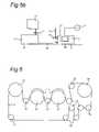
- FIG. 1shows a schematic view of various steps in a atomic layer deposition process for an exemplary embodiment in which an Al 2 O 3 layer is deposited on a substrate having SiOH groups as active surface sites;
- FIG. 2shows a time plot of gas flows in an embodiment of the present invention using a single treatment space
- FIG. 3shows a time plot of gas flows in a further embodiment of the present invention using a single treatment space
- FIG. 4shows a time plot of gas flows in an even further embodiment of the present invention using a single treatment space
- FIGS. 5 a and 5 bshow schematic views of an arrangement for processing a substrate according to the present invention
- FIG. 6shows a schematic view of an embodiment with a moving substrate using two treatment spaces
- FIG. 7shows an embodiment for an apparatus having a sequence of repeating treatment spaces
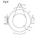
- FIG. 8shows an embodiment for continuous deposition process using two treatment spaces.
- an improved methodfor executing an atomic layer deposition (ALD) process with the aid of an atmospheric pressure plasma.
- ALD processesmay be used to deposit defect free coatings of atomic layers of a material such as Al 2 O 3 , HfO 2 , Ta 2 O 5 and many other materials.
- Prior art methodsneed a low pressure of typically between 50 mTorr and 10 Torr and/or high temperatures for proper operation.
- ALDatomic layer deposition
- CVDchemical vapor deposition
- PVDphysical vapor deposition
- ALDatomic layer deposition
- the intrinsic surface control mechanism of ALD processis based on the saturation of an individual, sequentially-performed surface reaction between the substrate and precursor molecules.
- the saturation mechanismmakes the film growth rate directly proportional to the number of reaction cycles instead of the reactant concentration or time of growth as in CVD and PVD.
- ALDis a self-limiting reaction process, i.e. the amount of precursor molecules attached to the surface is determined only by the number of reactive surface sites and is independent of the precursor exposure after saturation.
- the actual ALD cycleis composed of four steps, as shown in FIG. 1 for an exemplary atomic layer deposition of Al 2 O 3 on a fixed substrate 6 using tri-methyl-aluminum (TMA) as a precursor and water vapor as an reactive agent.
- TMAtri-methyl-aluminum
- Step AConditioning the surface 6 for atomic layer deposition by providing reactive surface sites, in this case hydroxyl groups on the Si substrate 6 surface, as shown indicated by (A) in FIG. 1 .
- Step BPrecursor dosing.
- precursor molecules (TMA)react with the reactive surface sites, as shown indicated by (B 1 ) in FIG. 1 .
- TMAprecursor molecules
- CH 4volatile other reaction products
- Step CA reactive agent (water vapor) is introduced near the substrate 6 surface and reacts with the monolayer of the precursor to form a monolayer of the desired material (Al 2 O 3 ), and more or less volatile reaction products (such as CH 4 ), as shown indicated by (C 1 ) in FIG. 1 .
- the surfaceremains populated with reactive sites in the form of hydroxyl groups attached to Al.
- the volatile reaction products and possibly unreacted agentsare purged out as indicated by (C 2 ) in FIG. 1 .
- the cycle of steps B and Cis repeated to deposit additional mono layers.
- one atomic layercan be deposited which allows a very accurate control of film thickness and film quality.
- the maximum growth rateis exactly one monolayer per cycle; however in most cases the growth rate is limited because of various reasons to 0.2-0.5 viz. 0.25-0.3 of a monolayer. One of these reasons may be the steric hindrance by the absorbed precursor molecules.
- an atmospheric pressure plasmais used in step C to accomplice the reactions.
- a reactive agentlike for example water vapor in the example shown in FIG. 1 , is inserted and the plasma is used to enhance removal of the ligands and replace these by other atoms or molecules.
- the ligandsare formed by the methyl groups and are replaced by oxygen atoms and hydroxyl groups. These hydroxyl groups are suitable for starting the process cycle again from step B.
- the ALD processcan be carried out as described in the prior art except that the standard low pressure inductively-coupled plasma (ICP) or RF plasma is substituted by an atmospheric pressure plasma step. As a result all the steps involved can now be carried out under atmospheric pressure.
- ICPinductively-coupled plasma
- RF plasmaRF plasma
- the present inventionmay be advantageously used when the substrate 6 is of a material which cannot withstand high temperature, such as polymer foil.
- the inventionis however not limited to polymer foils, as all kind of substrates 6 can be used bearing active sites on the surface.
- the substrates 6can be selected from for example ceramics, glasses, wafers, thermo-set and thermo-plast polymers and so on.
- the surface of the substrate to be usedis provided with reactive surface sites.
- Thiscan be done for example through a CVD step.
- the depositionshould be uniform and provide for a uniform distribution of the active sites over the substrate surface
- these active surface sitesare Si—OH groups.
- These Si—OH groupsare suitable for reaction with the precursor molecules.
- the surface of the substratecomprises active sites capable of reacting with a precursor molecule.
- such surface active sitewill comprise a hydroxyl group, while in another embodiment the active surface site might comprise a NH2- or NHR-group in which R can be a short chain aliphatic group or an aromatic group.
- These active groupsmight be linked to various atoms, like Si, Ti, Al, Fe and so on. Further active sites can be envisaged using P or S.
- step Bthe active surface sites of the substrate react with precursor molecules.
- precursor moleculesmay be selected from organometallic compounds and for example halides or substance comprising both halides and organic ligands.
- the elements of these precursorscan be selected from e.g.
- Precursor moleculescomprising more than one element can also be used. Examples for these molecules are:
- This step Bcan be done in a treatment space 5 (see e.g. description of FIG. 5 below), where the substrate 6 having the reactive site is positioned in a fixed position and not moving.
- the precursoris inserted in this treatment space 5 , after which the reaction occurs with the active surface sites.
- the precursoris added via an inert carrier gas.
- This inert carrier gascan be selected from the noble gasses and nitrogen. Also inert gas mixtures can be used as carrier gas.
- the concentration of the precursor in the carrier gascan be from 10 to 5000 ppm and should be sufficient to make the surface reaction complete. The reaction is in most cases instantaneous.
- the treatment space 5is purged or flushed with an inert gas or inert gas mixture, which may be the same gas or gas mixture used as a carrier gas for the precursor, but it may also be a different gas or gas mixture.
- This step Bis most preferably done at room temperature, but it can also be executed at elevated temperature, but should be in any case well below the temperature at which the substrate starts to deteriorate.
- the temperatureshould remain for example preferably below 80° C., but for example for wafers, glasses or ceramics, the temperature, if necessary, can be above 100° C.
- the substrate 6 provided with the precursor moleculescan be stored until the next step or can be subjected to the next step immediately.
- step C in the ALD processis done at elevated temperatures at sub atmospheric pressure.
- the precursor molecules attached to the substrate 6 via the active surface sitesare converted to a monolayer of the chemical compound which is formed from the precursor molecules after thermal reaction as such, a thermal reaction of the attached precursor with an reactive agent or a thermal reaction enhanced by a low pressure inductive coupled plasma or low pressure RF plasma.
- step Cis performed in general at elevated temperatures viz. over 100° C. and at low pressure to have a complete conversion of the precursor molecules to a monolayer of a chemical compound having active sites, suitable for another deposition step B.
- using the method of the prior artit is not possible to use a vast number of thermoplast polymers with relatively low glass temperature Tg as a substrate 6 due to the heating step.
- step Ccan be performed at moderate temperature at atmospheric pressure using an atmospheric plasma, where the plasma is generated in a gas mixture of a reactive agent and an inert gas or inert gas mixture.
- the inert gascan be selected from the noble gasses and nitrogen.
- the inert gas mixturescan be mixtures of noble gases or mixtures of noble gases and nitrogen.
- the concentration of the reactive agent in the gas or gas mixturecan be from 1% to 50%.
- the reactive agentbasically will react with ligands of the precursor molecule which in step B is attached via the active sites to the substrate 6 .
- This reactive agentcan be oxygen or oxygen comprising gases like ozone, water, carbon oxide or carbon dioxide.
- the reactive agentcan also comprise nitrogen comprising compounds such as NH3, nitrogen oxide, dinitrogen oxide, nitrogen dioxide and the like.
- the atmospheric pressure plasmais generated between two electrodes.
- the electrodeshave a surface area which is at least as big as the substrate surface covered with the precursor molecules
- the substrate 6can be fixed in the treatment space between the two electrodes.
- substrate 6is larger than the electrode area, the substrate 6 has to move through the electrode gap preferably at a linear speed.
- the atmospheric plasmacan be any kind of this plasma known in the art. Very good results are obtained using a pulsed atmospheric pressure glow discharge (APG) plasma. Until recently these plasma's suffered from a bad stability, but using the stabilization means as for example described in U.S. Pat. No. 6,774,569, EP-A-1383359, EP-A-1547123 and EP-A-1626613, very stable APG plasma's can be obtained. In general these plasma's are stabilized by stabilization means counteracting local instabilities in the plasma.
- APGatmospheric pressure glow discharge
- step Ca substrate is obtained with a monolayer of the chemical compound formed in step C.
- This monolayeron its turn again has active sites suitable for repeating steps B and C, by which several monolayers can be applied to the substrate one above the other; 10, 20, 50, 100 and even as much as 200 layers can be applied one above the other.
- mono-layers of different compositioncan be applied one above the other, by which very specific properties can be obtained.
- the stepsare performed in one single treatment space 5 (see e.g. the embodiment described with reference to FIG. 5 a below).
- the substrate 6is in a fixed position in the treatment space 5 .
- step Bthe deposition of precursor molecules
- step Ctreatment with atmospheric plasma
- the substrate 6can be in a fixed position but might also have a linear speed depending on the size of the substrate 6 compared to the size of the electrodes.
- the treatment spaceis flushed with the inert gas (mixture), after which an inert gas (mixture) comprising an active gas is introduced in the treatment space, the plasma is ignited and the substrate 6 , in case the substrate is larger in size than the electrode, is moved with a linear speed through the plasma space. After this the treatment space 5 is again flushed with an inert gas (mixture) and the steps B and C can be repeated until the wanted number of monolayers is obtained.
- the inert gasmixture
- the steps B and Ccan be repeated until the wanted number of monolayers is obtained.
- the precursor materialis provided in the gas (mixture) in a pulsed manner, and the reactive agent is introduced in a gas mixture with an inert gas or inert gas mixture also in a pulsed manner, the method further comprising removing excess material and reaction products using an inert gas or inert gas mixture after each pulsed provision of precursor material and pulsed introduction of the reactive agent.
- TMAis used as precursor
- argonas flushing gas
- oxygenreactive agent
- the precursor material(TMA in this example) is provided in a gas mixture with an inert gas in a pulsed manner and the reactive agent (oxygen) is supplied in a continuous manner in the inert gas mixture (with argon), meaning that the inert gas mixture which is inserted in the treatment space 5 comprises the reactive agent continuously, while the precursor is added discontinuously.
- the gas supply methodis somewhat simpler than in the first embodiment. In this method excess material and reaction products are purged from the treatment space using an inert gas or inert gas mixture including the reactive agent after each pulsed provision of precursor material and pulsed application of the discharge plasma.
- the precursor materialis provided in a continuous manner in an inert gas mixture in a first layer near the surface of the substrate only, and the reactive agent (oxygen) is introduced in a gas mixture with an inert gas (argon) or inert gas mixture in a continuous manner in a second layer above the first layer.
- laminar flowis a prerequisite.
- This embodimentis advantageously applied when precursor and reactive agent do not or not substantially react with each other.
- the atmospheric plasma treatmentis done in a pulsed manner, by which the method comprises a plasma off time, allowing the precursor to react with active surface sites and a plasma on time where the precursor molecules attached to the surface are converted to the required chemical substance.
- the compositions of the various gas mixturesdo not change during the process, control of the flow is important in order to provide a laminar flow.
- the embodiments described aboveare all applicable in case of the availability of one treatment space 5 .
- the methodcan also be applied when using at least two treatment spaces 1 , 2 in which a first treatment space 1 is used for the reaction of the precursor with the active surface sites, while the second treatment space 2 is used for the atmospheric plasma treatment (see embodiment of FIGS. 5B , and 6 described below).
- the control of the gas compositions and the gas flowsis easier and higher efficiencies can be obtained.
- the substrate 6is moved continuously through the treatment spaces 1 and 2 .
- a moving speed of 1 m/minis quite common, but higher speeds like 10 m/min can be used, while in specific cases a speed as high as 100 m/min can be used.
- the gas flow in this embodimentmay be continuous: in treatment space 1 an inert gas (mixture) including the precursor and in treatment space 2 an inert gas (mixture) including a reactive agent is inserted.
- a further advantage of this embodimentis that the temperature in the first treatment space 1 and the second treatment space 2 need not to be the same, however in case of polymeric substrates the temperature should preferably be below the glass transition temperature which might be below 100° C. for one polymeric substrate, but it might be also above 100° C. in both treatment spaces 1 , 2 .
- the substrate 6is not moving continuously, but intermittently, from one treatment space to the other, while during treatment the substrate 6 is not moving.
- treatment spaces 1 and 2 and the substrate 6 to be treatedform a loop, by which sequences of step B and step C can be repeated in principle endlessly.
- An implementation of this embodimentis shown schematically in FIG. 6 and FIG. 8 , which will be described in more detail below.
- first treatment spaces 1 and second treatment spaces 2are arranged after each other.
- various monolayers of the same or different compositioncan be applied over each other using a continuous process.
- the treatment spaces 1 , 2can be arranged in a linear manner, circular manner or any other arrangement suitable in a continuous process.
- a sub atmospheric pressure plasmamay be used at pressures as for example 1 Torr or, 10, 20 or 30 Torr.
- treatment spaces 1 and 2are decoupled, meaning that first in treatment space 1 a precursor molecule is attached to the active sites of a substrate 6 , that this modified substrate 6 is stored under conditions where this substrate 6 is stable, and that at another time the substrate 6 is treated in treatment space 2 , where it is subjected to the plasma treatment.
- the inventionis also directed to an apparatus arranged to perform the methods of the present invention.
- the apparatuscomprises a treatment space 5 and a plasma generator 10 for generating an atmospheric pressure plasma in the treatment space 5 in which the substrate 6 may be placed.
- the substrate 6may act as the dielectric of one of the electrodes of the plasma generator (as indicated by the grounding of substrate 6 in FIG. 5 a ).
- the atmospheric plasmamay be generated in the treatment space 5 between two electrodes.
- the apparatusfurther comprises gas supply means 15 .
- the various components used in this embodimentare injected in the space 5 , e.g. using a gas box or gas supply means 15 .
- the gas supply means 15may comprise various gas containers, being provided with mixing means, capable of homogeneously mixing the various gas components accurately providing at the same time various mixtures of different composition or providing various gas mixtures sequentially and capable of maintaining a stable gas flow over a prolonged period of time.
- the gas supply means 15could consist of a gas shower head with two, three or more outlets where the precursor, reactive, purging gas can be supplied to the process through pulsing. However, thorough mixing is crucial for the uniformity of the deposits.
- valves 17 , 18are used in case of the embodiments of FIGS. 2 and 3 described above, in which one or more gas streams are applied in a pulsed manner.
- the various gas mixturescan be prepared at the same time, meaning, that the sequence of gas additions is controlled by a (set of) valve(s) 17 .
- the valve 17is switched to the gas mixture comprising the precursor allowing a gas pulse comprising precursor, after this pulse this valve 17 (or another valve 17 ) is switched to an inert gas composition for purging, after which the valve 17 is switched to the gas composition including the reactive agent to execute step C.
- valve 17is switched to an inert gas composition for another purge step.
- the valves 17which are known as such to the person skilled in the art, and thus not discussed in further detail, are installed as close as possible to the treatment space 5 to prevent mixing and to reduce delay time in the gas flows. To limit gas mixing due to diffusion, rather high gas flows are required >1 m/s.
- the precursor injection for the embodiment as shown in FIG. 5 ashould be as near as possible to the substrate 6 surface to confine the precursor flows and limit the diffusion. In such a manner the ALD mode can be maintained.
- the precursor gasis injected in the space 5 using for example a separate injection channel 16 , as shown in FIG. 5 a , which is provided with its own valve 18 .
- the apparatusmay comprise moving means for moving the substrate 6 with a linear speed through the treatment space 5 , e.g. in the form of a transport mechanism.
- the apparatuscomprises a first treatment space 1 which is provided with gas supply means 15 for providing various gas mixtures to the treatment space 1 .
- the gas mixturescan comprise a precursor and an inert gas or inert gas mixture, or an inert gas or inert gas mixture.
- the gas supply means 15may comprise various gas containers, and the gas supply means 15 may comprise mixing means, capable of homogeneously mixing the various gas components accurately providing at the same time various mixtures of different composition or providing different gas mixtures sequentially and capable of maintaining a stable gas flow over a prolonged period of time.
- the sequence of gas additionscan be controlled by a (set of) valve(s) 17 .
- the valve 17is switched to the gas mixture comprising the precursor allowing a gas pulse comprising precursor material, after this pulse this valve 17 or another valve (not shown) is switched to an inert gas composition for purging.
- the apparatus in this embodimentcomprises a second treatment space 2 which is provided with a plasma generator 10 for generating an atmospheric pressure plasma and an injection channel 16 for providing various gas mixtures to the second treatment space 2 .
- the gas mixturecomprises a mixture of a reactive agent and an inert gas or inert gas mixture, or an inert gas or inert gas mixture.
- the injection channel 16may be connected to further gas supply means, which again may comprise various gas containers and mixing means capable of homogeneously mixing the various gas components accurately providing at the same time various mixtures of different composition or providing various gas mixtures sequentially and capable of maintaining a stable gas flow over a prolonged period of time.
- the sequence of gas additionscan be controlled by a(set of) valve(s) 18 .
- the valve 18is switched to the gas composition including the reactive agent to execute step C by igniting the atmospheric discharge plasma and as the final step the valve 18 is switched to an inert gas composition for the purging step.
- the apparatusfurther comprises transport means 20 to move the substrate 6 from the first treatment space 1 to the second treatment space 2 , e.g. in the form of a transport robot.
- FIGS. 5 a and 5 bhave the following common elements.
- An apparatus for atomic layer deposition on a surface of a substrate 6 in a treatment space 1 , 2 ; 5the apparatus comprising a gas supply device 15 , 16 for providing various gas mixtures to the treatment space 1 , 2 ; 5 , the gas supply device 15 , 16 being arranged to provide a gas mixture comprising a precursor material to the treatment space 1 , 2 ; 5 for allowing reactive surface sites to react with precursor material molecules to give a surface covered by a monolayer of precursor molecules attached via the reactive sites to the surface of the substrate 6 .
- a gas mixturecomprising a reactive agent capable to convert the attached precursor molecules to active precursor sites
- the apparatusfurther comprises a plasma generator 10 for generating an atmospheric pressure plasma in the gas mixture comprising the reactive agent.
- the gas supply device 15 , 16is provided with a valve device 17 , 18 , the gas supply device 15 , 16 being arranged to control the valve device 17 , 18 for providing the various gas mixtures continuously or in a pulsed manner and for removing excess material and reaction products using an inert gas or inert gas mixture.
- the gas supply device 15 , 16comprises an injection channel 16 having a injection valve 18 positioned near the surface of the substrate 6 , in which the gas supply device 15 , 16 is arranged to control the valve device 17 and the injection valve 18 for providing the precursor material in a continuous manner in a first layer near the surface of the substrate 6 only using the introduction channel 16 , and for introducing the reactive agent in a gas mixture with an inert gas or inert gas mixture in a continuous manner in a second layer above the first layer.
- the transport means 20are arranged to move the substrate 6 continuously with a linear speed or intermittently from the first treatment space 1 to second treatment space 2 (and vice versa for repeating the steps B and C of the present invention).
- FIG. 6A further apparatus embodiment in which the substrate 6 is provided in the form of an endless web substrate is shown schematically in FIG. 6 .
- the apparatuscomprises two main drive cylinders 31 , and 32 , which drive the substrate 6 via tensioning rollers 33 and treatment rollers 34 and 35 .
- the treatment roller 34drives the substrate 6 along the first treatment space 1 for performing step B of the present invention
- treatment roller 35drives the substrate 6 along the second treatment space 2 for performing step C of the present invention.
- the substrate 6is wrapped around a cylinder 51 which can be rotated as shown in FIG. 8 .
- the substrate 6passes treatment space 1 for performing step B of the present invention and upon further rotation it passes treatment space 2 for performing step C of the present invention.
- a continuous deposition of atomic layerscan be achieved.
- Driving the cylinder 52may be achieved using a motor 53 driving a drive shaft 52 connected to the cylinder 52 as shown in FIG. 8 . Flushing of the substrate 6 may be obtained at the stages where no treatment space 1 or 2 is present around the cylinder 52 , as indicated by reference numeral 50 in FIG. 8 .
- the apparatusis composed of a sequence of first and second treatment spaces 1 and 2 (or alternatively treatment spaces 47 ) as shown in the various embodiments shown schematically in FIGS. 7 a, b and c .
- a substrate 6 in the form of a web or the likeis transported from an unwinder roller 41 to a winder roller 42 .
- a number of tensioning rollers 46are positioned. This will allow moving the substrate 6 continuously with linear speed or intermittently in the sequence of first and second treatment spaces 1 and 2 .
- the various treatment spaces 1 , 2are equipped with a lock to keep the precursor and the reactive agent in a confined area.
- the apparatus of this embodimentis very suitable to deposit various layers on a flexible substrate in which the substrate 6 to be treated is unwound from the unwind roll 41 and the treated substrate 6 is wound on a wind roll 42 again.
- the substrate 6is first treated in a pretreatment space 45 , e.g. to execute the first pretreatment step A according to the present invention, as described above. Then, the substrate 6 moves along tensioning roller 46 to a first treatment sequence roller 43 . Along the outer perimeter of the first treatment sequence roller 43 , a sequence of first and second treatment spaces 1 , 2 are positioned, in the shown embodiment two pairs, which allow providing two atomic layers on the substrate 6 . The substrate 6 is then moved along further tensioning rollers 46 to a further treatment sequence roller 44 (or even a plurality of further treatment sequence rollers 44 ), which is also provided with a sequence of first and second treatment spaces 1 , 2 .
- FIG. 7 ban alternative arrangement is shown schematically.
- a large number of tensioning rollers 46are provided in between the unwind roller 41 and wind roller 42 .
- a pretreatment space 45is provided, in which step A of the present invention is applied to the substrate 6 .
- treatment spaces 47may be provided, at which both steps B and C are applied to the substrate 6 .
- the subsequent treatment spaces 47may be arranged to apply step B or step C in an alternating manner.
- FIG. 7 can even further alternative arrangement is shown schematically.
- a number of tensioning rollers 46are provided in between the unwind roller 41 and wind roller 42 .
- a first treatment space 1 or a second treatment space 2is provided to apply step B and step C of the present invention in an alternating manner.
- the used plasma for the apparatus embodimentsis preferably a continuous wave plasma.
- a more preferred plasmamay be a pulsed atmospheric discharge plasma or a pulsed atmospheric glow discharge plasma.
- Even more preferredis the use of a pulsed atmospheric glow discharge plasma characterized by an on time and an off time
- the on-timemay vary from very short, e.g. 20 ⁇ s, to short, e.g. 500 ⁇ s. this effectively results in a pulse train having a series of sine wave periods at the operating frequency, with a total duration of the on-time
- the circuitry used in the set-up for the atmospheric glow discharge plasmais preferably provided with stabilization means to counteract instabilities in the plasma.
- the plasma electrodecan have various lengths and widths and the distance between the electrodes may depend on the substrate used. Preferably the electrode gap is less than 3 mm allowing substrates as thick as 2 mm to be treated, more common is an electrode gap of 1 mm allowing for a substrate thickness as high as 0.5 mm.
- treatment space 2may be arranged in such a way, that it is also possible to use a sub atmospheric glow discharge plasma at for example pressures of 1 Torr or 10, 20, 30 Torr.
- the present inventionmay be applied advantageously in various ALD applications.
- the inventionis not limited to semiconductor applications, but may also extend to other applications, such as packaging, plastic electronics like organic LED's (OLED's) or organic thin film transistor (OTFT) applications.
- OLED'sorganic LED's
- OTFTorganic thin film transistor
- high quality photo-voltaic cellsmay be manufactured on flexible substrates.
- the method and apparatus of the present inventioncan be used in any application which requires the deposition of various monolayers on a substrate.
- VTRwater vapor transmission rate
- Step AThe polymer surface is made susceptible to the ALD reaction by a short CVD step in which a very thin film of SiO2 is deposited from TEOS (tetraethoxysilane) or HMDSO (hexamethyldisiloxane).
- TEOStetraethoxysilane
- HMDSOhexamethyldisiloxane
- Step BIn a first embodiment pulses of TMA precursor and oxygen gas are alternated while maintaining a purge step in between precursor and reactive agent to flush the electrode gap (above the surface of the substrate 6 ).
- the purge stepmay be performed using an inert gas, in this case Ar. This is shown schematically in the time plot of FIG. 2 , which shows the respective gas flows and APG plasma pulse for a single cycle time period. Due to atmospheric pressure TMA is reacting very quickly with the hydroxyl groups. Typical concentration of TMA is 200 mg/hr.
- Step CAfter flushing the gap to remove the precursor the oxygen is inserted in a concentration of 10% in argon. Subsequently the stabilized atmospheric glow discharge plasma is ignited either in a single pulse trains or in a short sequence of pulse trains to fully oxidize the surface of the substrate 6 . This is illustrated in the table below for an example with a cycle time of 1 second.
- the plasma conditions in this embodimentwere the use of a dielectric barrier discharge geometry, a frequency of 150 kHz, and a gap width between a DBD electrode and the substrate 6 of 1 mm.
- the total plasma treatment time usedis 100 ms.
- a continuous reactive (for instance 10% oxygen in argon) gas streamis used, during both step A and step B, while a pulsed TMA precursor treatment is used, as shown schematically in FIG. 3 .
- a pulsed TMA precursor treatmentis used, as shown schematically in FIG. 3 .
- Argon and Oxygenare introduced in a continuous manner.
- the plasma conditions in this embodimentare the same as described with the previous embodiment.
- the input of TMAis in a continuous manner, and only the APG plasma is applied in a pulsed manner to enhance the ALD process, as shown in the time plot of FIG. 4 .
- the TMA flowshould be limited to a region very nearby the surface 6 on which the Al 2 O 3 has to be deposited. This embodiment allows for obtaining a very short cycle time of only 0.3 sec, as shown in the following table.
- a precursor reaction stationor first treatment space 1
- a reactive agent stationor second treatment space 2
- this simple set upwas used for depositing the inorganic layer on a polymer substrate.
- a dancer roll systemcomprising the tensioning rollers 46 was used to maintain a good web alignment. By transporting the polymer sheet 20, 50 and 100 times through the ALD process line very uniform coatings were achieved.
- Typical line speedwas 1 m/min. Plasma was stabilized using displacement current control to maintain uniform discharge thus increasing the reaction rate on the surface.
- Layer thicknesswas characterized by in-line Spectroscopic Ellipsometry (SE) to determine layer growth as a function of the number of passes through the ALD process.
- SEin-line Spectroscopic Ellipsometry
- WVTRwater vapour transmission rate
- the layer thickness growthis linear with the number of passes which indicates that during each cycle one atomic layer is deposited. Furthermore it can be seen that the WVTR performance of the inorganic layer improves as a function of the layer thickness.
Landscapes
- Chemical & Material Sciences (AREA)
- Engineering & Computer Science (AREA)
- Metallurgy (AREA)
- General Chemical & Material Sciences (AREA)
- Chemical Kinetics & Catalysis (AREA)
- Materials Engineering (AREA)
- Mechanical Engineering (AREA)
- Organic Chemistry (AREA)
- Plasma & Fusion (AREA)
- Physics & Mathematics (AREA)
- Electromagnetism (AREA)
- Chemical Vapour Deposition (AREA)
- Formation Of Insulating Films (AREA)
Abstract
Description
- The present invention relates to a method for atomic layer deposition on the surface of a substrate. In a further aspect, the present invention relates to an apparatus for atomic layer deposition on the surface of a substrate including an atmospheric plasma system. In an even further aspect of this invention, the apparatus is used for the deposition of a chemical substance or element.
- Atomic layer deposition (ALD) is used in the art to provide layers of a material on the surface of a substrate. Different from chemical vapor deposition (CVD) and physical vapor deposition (PVD), atomic layer deposition (ALD) is based on saturated surface reactions. The intrinsic surface control mechanism of ALD process is based on the saturation of an individual, sequentially-performed surface reaction between the substrate reactive sites and precursor molecules. The saturation mechanism makes the film growth rate directly proportional to the number of reaction cycles instead of the reactant concentration or time of growth as in CVD and PVD.
- American patent publication US2005/0084610 discloses a chemical vapor deposition process for atomic layer deposition on the surface of a substrate. The deposition process is made more effective using a radical generator during the deposition process, e.g. a plasma generator, such as an atmospheric pressure glow discharge plasma. In the process disclosed, the precursor molecules are decomposed before reacting with the surface.
- ALD is a self-limiting reaction process, i.e. the amount of deposited precursor molecules is determined only by the number of reactive surface sites on the substrate surface and is independent of the precursor exposure after saturation. In theory, the maximum growth rate is exactly one monolayer per cycle, however in most cases because of various reasons the growth rate is limited to 0.2-0.3 of a monolayer. The ALD cycle is composed of four steps. In general it is performed in one single treatment space. It starts as
step 1 with providing the surface of a substrate with reactive sites. As a next step a precursor is allowed to react with the reactive sites and the excess material and reaction products are purged out of the treatment space and, ideally, a monolayer of precursor remains attached to the substrate surface via the reactive surface sites (step 2). A reactive agent is introduced into the treatment space and reacts with the attached precursor molecules to form a monolayer of the desired material having reactive sites again (step 3), after which unreacted material and by-product is purged out. Optionally the cycle is repeated to deposit additional monolayers (step 4). With each cycle basically one atomic layer can be deposited which allows a very accurate control of film thickness and film quality. - In the prior art, several methods have been developed to enhance the reaction step in this ALD process, e.g. thermal ALD and plasma assisted ALD. The plasma as used in known ALD methods may be a low pressure RF plasma or an inductively coupled plasma (ICP), and may be used to deposit Al2O3, HfO2, Ta2O5and many other materials.
- International patent publication WO01/15220 describes a process for deposition of barrier layers in integrated circuits, in which ALD is used. In the ALD steps, low pressure is used (of about 10 Torr (1330 Pa)) in combination with a thermal reaction step at a high temperature (up to 500° C.). Alternatively it is suggested to use a plasma to produce a reactive environment. All disclosed embodiments describe a very low pressure environment, requiring special measures in the apparatus used.
- US patent application US2004/0219784 describes methods for forming atomic layers and thin films, using either thermal reaction steps, or plasma assisted reaction steps, in which radicals are formed remotely form the substrate and transported thereto. Again, these processes are performed at relatively high temperature (100-350° C.) and low pressure (almost vacuum, typically 0.3 to 30 Torr (40 to 4000 Pa)).
- US patent application US2003/0049375 discloses a CVD process to deposit a thin film on a substrate using a plasma assisted CVD process. The formation of a plurality of atomic layers is claimed.
- The known ALD methods as described above are mainly performed under low pressure conditions, and usually require vacuum equipment. Furthermore, the ALD methods described using thermal reaction steps (at temperatures well above room temperature, e.g. even 300-900° C.), are not suitable for deposition of material on temperature sensitive substrates, such as polymer substrates.
- According to the present invention, it has been surprisingly found that plasma enhanced ALD using an atmospheric pressure plasma can also be used. Therefore, a method according to the preamble above is provided, comprising conditioning the surface for atomic layer deposition by providing reactive surface sites (step A), providing a precursor material to the surface for allowing reactive surface sites to react with precursor material molecules to give a surface covered by a monolayer of precursor molecules attached via the reactive sites to the surface of the substrate (step B); and subsequently exposing the surface covered with precursor molecules to an atmospheric pressure plasma generated in a gas mixture comprising a reactive agent capable to convert the attached precursor molecules to active precursor sites (step C). The steps of providing precursor material and of exposing the surface to an atmospheric pressure plasma may be repeated consecutively in order to obtain multiple layers of material on the substrate surface. It is noted that during step C, i.e. the application of the atmospheric pressure plasma, no precursor molecules are present, as the plasma step is used to perform a surface dissociation reaction. This dissociation reaction may be supported using a reactive molecule like oxygen, water, etc.
- Using this method a single atomic layer of reacted precursor, or two or more atomic layers of reacted precursor can be attached to the surface, where each layer might comprise a different reacted precursor.
- After providing the precursor material to the surface (step B of this method), precursor molecules react with reactive substrate surface sites.
- In a further embodiment a purging step using an inert gas or inert gas mixture may be used hereafter to remove the excess of precursor molecules and/or the molecules formed in this reaction.
- When the surface is exposed to the atmospheric plasma (step C of this method) a reactive step takes place in which the precursor molecules attached to the substrate surface via the reactive surface sites are converted to reactive precursor surface sites. In a further embodiment, the more or less volatile molecules formed at this stage may be removed via a purging step using an inert gas or inert gas mixture.
- Use of an atmospheric plasma obviates the need to work at very low pressure. All steps of the ALD process can now be executed at around atmospheric pressure. Hence no complex constructions are necessary to obtain a vacuum or near vacuum at the substrate surface during processing.
- In an embodiment, the substrate is a flexible substrate of polymeric material. The present treatment method is particularly suited for such a substrate material, with regard to the operating environment (temperature, pressure) allows the use of such material without necessitating further measures. The present electrode structure also allows a wider gap between electrodes than in prior art systems, allowing using a substrate with a thickness of up to 2 mm.
- In a further embodiment, the reactive agent is a reactive gas, such as oxygen, an oxygen comprising agent, a nitrogen comprising agent, etc. The precursor material is e.g. tri-methyl-aluminum (TMA), which allows growing Al2O3layers on e.g. a Si substrate. The reactive agent mixture may in a further embodiment comprise an inert gas selected from a noble gas, nitrogen or a mixture of these gases.
- Conditioning the surface of the substrate for atomic layer deposition may in an embodiment of the present invention comprise providing the surface with reactive groups, such as OH-groups or NH2-groups, etc.
- The used atmospheric plasma can be any atmospheric plasma known in the art.
- In a specific embodiment of this invention the atmospheric plasma is an atmospheric pressure glow discharge plasma. In a further embodiment, the atmospheric pressure glow discharge plasma is stabilized by stabilization means counteracting local instabilities in the plasma.
- Executing an ALD process at atmospheric pressure has an additional advantage in that higher reaction rates are possible, which can lead to a higher productivity. With the present method, parallel thin film layers for example as thin as one molecular layer may be obtained, wherein the films have a comparable or better performance to films produced by prior art methods.
- In cases, where the substrate cannot withstand high temperatures, prior art ALD methods cannot be used. Using a plasma at atmospheric pressure, the ALD process may even be executed at room temperature, which allows a much larger area of applications, including the deposition of thin layers on synthetic materials such as plastics. This also allows applying the present method for processing of e.g. polymer foils. The substrates used in the deposition process of this invention are not limited to these foils and can include wafers, ceramics, plastics and the like.
- In one embodiment of the present invention the substrate is in a fixed position and steps B and C are performed in the same treatment space
- The precursor material is provided in a gas mixture with an inert gas (such as Ar, He, N2) in a pulsed manner in a further embodiment, and the reactive agent is introduced in a gas mixture with an inert gas or inert gas mixture in a pulsed manner. This method further comprises removing excess material and reaction products using an inert gas or inert gas mixture after each pulsed provision of precursor material and pulsed introduction of the reactive agent.
- In an alternative embodiment, the precursor material is provided in a gas mixture with an inert gas or inert gas mixture in a pulsed manner, and the reactive agent is introduced in a gas mixture with an inert gas or inert gas mixture in a continuous manner, and the method further comprises removing excess material and reaction products using an inert gas or inert gas mixture after the pulsed provision of precursor material, and during the application of the atmospheric pressure glow discharge plasma.
- In a further alternative embodiment, the precursor material is provided in a continuous manner in a first layer near the surface of the substrate only, and the reactive agent is introduced in a gas mixture with an inert gas or inert gas mixture in a continuous manner in a second layer above the first layer.
- In another embodiment the substrate is moving, either continuously or intermittently. In this case step B may be done in a first treatment space and step C is done in another, second treatment space. In a further embodiment, a continuous or pulsed flow of a mixture of precursor material and an inert gas or inert gas mixture is provided in the first treatment space and a continuous or pulsed flow of a mixture of a reactive agent and an inert gas or inert gas mixture is provided in the second treatment space.
- According to a further embodiment, the precursor material is provided in a concentration of between 10 and 5000 ppm. This concentration is sufficient to obtain a uniform layer of precursor molecules on the substrate surface in step B of the present method.
- In an even further embodiment, the gas mixture of the reactive agent and inert gas comprises between 1 and 50% reactive agent. This is sufficient to have a good reaction result in step C of the present method.
- The invention is furthermore directed to an apparatus which is capable of executing the method of this invention.
- An embodiment of the present invention relates to an apparatus for atomic layer deposition on a surface of a substrate in a treatment space, the apparatus comprising a gas supply device for providing various gas mixtures to the treatment space, the gas supply device being arranged to provide a gas mixture comprising a precursor material to the treatment space for allowing reactive surface sites of the substrate to react with precursor material molecules to give a surface covered by a monolayer of precursor molecules attached via the reactive sites to the surface of the substrate, and to provide a gas mixture comprising a reactive agent capable to convert the attached precursor molecules to active precursor sites, the apparatus further comprising a plasma generator for generating an atmospheric pressure plasma in the gas mixture comprising the reactive agent in the treatment space. The treatment space may be a controlled enclosure, e.g. a treatment chamber, or a controlled treatment location, e.g. as part of a substrate web.
- In one embodiment, the apparatus is specifically designed to perform steps B and C of the present method in one single treatment space. For this, the apparatus further comprising a first treatment space in which the substrate is positioned in operation, the gas supply device being further arranged to perform any one of the relevant method claims.
- In another embodiment the apparatus is designed with two different treatment spaces, one for step B and one for step C. In this embodiment, the apparatus further comprises a first treatment space in which the substrate is subjected to the gas mixture comprising a precursor material, a second treatment space in which the substrate is subjected the gas mixture comprising the reactive agent and the atmospheric pressure plasma, and a transport device for moving the substrate between the first and second treatment spaces. The gas supply device may be arranged to apply the relevant method embodiments described above which utilize two treatment spaces, including flushing steps to remove excess of reactants and or formed reaction products.
- In still another embodiment the apparatus is designed in such a way to have a multiple sequence of treatment spaces for step B and step C. E.g., a plurality of first and second treatment spaces are placed sequentially one behind the other in a circular or linear arrangement.
- The above apparatus embodiments may be designed in such a way, that the substrate may comprise a continuous moving web or an intermittently moving web.
- In a further embodiment, the gas supply device is provided with a valve device, the gas supply device being arranged to control the valve device for providing the various gas mixtures continuously or in a pulsed manner and for removing excess material and reaction products using an inert gas or inert gas mixture. The valve device may comprise one or more valves.
- An even further embodiment is especially suited to ensure that the precursor material is kept near to the substrate surface. To this end, the gas supply device comprises an injection channel having a injection valve positioned near the surface of the substrate, in which the gas supply device is arranged to control the valve device and the injection valve for providing the precursor material in a continuous manner in a first layer near the surface of the substrate only using the introduction channel, and for introducing the reactive agent in a gas mixture with an inert gas or inert gas mixture in a continuous manner in a second layer above the first layer.
- In a further embodiment, the plasma generator is arranged to generate an atmospheric pressure glow discharge plasma. The plasma generator may further comprise stabilization means for stabilizing the pulsed atmospheric glow discharge plasma to counteract local instabilities in the plasma.
- Furthermore the invention is directed to the use of the apparatus of this invention, e.g. for depositing a layer of material on a substrate. The substrate may be a synthetic substrate, e.g. on which an electronic circuit is to be provided, such as for the production of organic LEDs or organic TFTs. The substrate may be a flexible substrate, e.g. of a polymeric material. The thickness of the substrate may be up to 2 mm. These types of substrates are specifically suited to be treated using the present invention embodiments, whereas treatment in prior art systems and methods was not practical or even impossible. Alternatively, the plasma deposition apparatus is used to produce flexible photo-voltaic cells on a flexible substrate. Also, the present invention relates to substrates provided with atomic layers deposited using the apparatus and method of this invention.
- The present invention will be discussed in more detail below, with reference to the attached drawings, in which
FIG. 1 shows a schematic view of various steps in a atomic layer deposition process for an exemplary embodiment in which an Al2O3layer is deposited on a substrate having SiOH groups as active surface sites;FIG. 2 shows a time plot of gas flows in an embodiment of the present invention using a single treatment space;FIG. 3 shows a time plot of gas flows in a further embodiment of the present invention using a single treatment space;FIG. 4 shows a time plot of gas flows in an even further embodiment of the present invention using a single treatment space;FIGS. 5 aand5b, show schematic views of an arrangement for processing a substrate according to the present invention;FIG. 6 shows a schematic view of an embodiment with a moving substrate using two treatment spaces;FIG. 7 shows an embodiment for an apparatus having a sequence of repeating treatment spaces; andFIG. 8 shows an embodiment for continuous deposition process using two treatment spaces.- According to the present invention, an improved method is provided for executing an atomic layer deposition (ALD) process with the aid of an atmospheric pressure plasma. ALD processes may be used to deposit defect free coatings of atomic layers of a material such as Al2O3, HfO2, Ta2O5and many other materials. Prior art methods need a low pressure of typically between 50 mTorr and 10 Torr and/or high temperatures for proper operation.
- Different from chemical vapor deposition (CVD) and physical vapor deposition (PVD), atomic layer deposition (ALD) is based on saturated surface reactions. The intrinsic surface control mechanism of ALD process is based on the saturation of an individual, sequentially-performed surface reaction between the substrate and precursor molecules. The saturation mechanism makes the film growth rate directly proportional to the number of reaction cycles instead of the reactant concentration or time of growth as in CVD and PVD.
- ALD is a self-limiting reaction process, i.e. the amount of precursor molecules attached to the surface is determined only by the number of reactive surface sites and is independent of the precursor exposure after saturation.
- The actual ALD cycle is composed of four steps, as shown in
FIG. 1 for an exemplary atomic layer deposition of Al2O3on a fixedsubstrate 6 using tri-methyl-aluminum (TMA) as a precursor and water vapor as an reactive agent. - Step A: Conditioning the
surface 6 for atomic layer deposition by providing reactive surface sites, in this case hydroxyl groups on theSi substrate 6 surface, as shown indicated by (A) inFIG. 1 . - Step B: Precursor dosing. During this step precursor molecules (TMA) react with the reactive surface sites, as shown indicated by (B1) in
FIG. 1 . This results in a precursor molecule attached via the reactive sites to thesubstrate 6 together with more or less volatile other reaction products, such as CH4. These volatile products, together with possible excess material are purged out of the treatment space and, ideally, a monolayer of precursor remains attached to thesubstrate 6 surface, as shown indicated by (B2) inFIG. 1 . - Step C: A reactive agent (water vapor) is introduced near the
substrate 6 surface and reacts with the monolayer of the precursor to form a monolayer of the desired material (Al2O3), and more or less volatile reaction products (such as CH4), as shown indicated by (C1) inFIG. 1 . The surface remains populated with reactive sites in the form of hydroxyl groups attached to Al. The volatile reaction products and possibly unreacted agents are purged out as indicated by (C2) inFIG. 1 . - Optionally the cycle of steps B and C is repeated to deposit additional mono layers. With each cycle one atomic layer can be deposited which allows a very accurate control of film thickness and film quality. In theory, the maximum growth rate is exactly one monolayer per cycle; however in most cases the growth rate is limited because of various reasons to 0.2-0.5 viz. 0.25-0.3 of a monolayer. One of these reasons may be the steric hindrance by the absorbed precursor molecules.
- According to the present invention, an atmospheric pressure plasma is used in step C to accomplice the reactions. During step C, a reactive agent like for example water vapor in the example shown in
FIG. 1 , is inserted and the plasma is used to enhance removal of the ligands and replace these by other atoms or molecules. In the exemplary case described above using TMA as precursor, the ligands are formed by the methyl groups and are replaced by oxygen atoms and hydroxyl groups. These hydroxyl groups are suitable for starting the process cycle again from step B. - The ALD process can be carried out as described in the prior art except that the standard low pressure inductively-coupled plasma (ICP) or RF plasma is substituted by an atmospheric pressure plasma step. As a result all the steps involved can now be carried out under atmospheric pressure.
- The present invention may be advantageously used when the
substrate 6 is of a material which cannot withstand high temperature, such as polymer foil. The invention is however not limited to polymer foils, as all kind ofsubstrates 6 can be used bearing active sites on the surface. Thesubstrates 6 can be selected from for example ceramics, glasses, wafers, thermo-set and thermo-plast polymers and so on. - In step A of the inventive method, the surface of the substrate to be used is provided with reactive surface sites. This can be done for example through a CVD step. During this CVD step the deposition should be uniform and provide for a uniform distribution of the active sites over the substrate surface In the example of
FIG. 1 these active surface sites are Si—OH groups. These Si—OH groups are suitable for reaction with the precursor molecules. This invention is however not limited to this specific embodiment. What is essential is that the surface of the substrate comprises active sites capable of reacting with a precursor molecule. In one embodiment such surface active site will comprise a hydroxyl group, while in another embodiment the active surface site might comprise a NH2- or NHR-group in which R can be a short chain aliphatic group or an aromatic group. These active groups might be linked to various atoms, like Si, Ti, Al, Fe and so on. Further active sites can be envisaged using P or S. - In step B, the active surface sites of the substrate react with precursor molecules. These precursor molecules may be selected from organometallic compounds and for example halides or substance comprising both halides and organic ligands. The elements of these precursors can be selected from e.g. cobalt, copper, chromium, iron, aluminum, arsenic, barium, beryllium, bismuth, boron, nickel, gallium, germanium, gold, hafnium, lead, magnesium, manganese, mercury, molybdenum, niobium, osmium, phosphorous, platinum, ruthenium, antimony, silicon, silver, sulpher, tantalum, tin, titanium, tungsten, vanadium, zinc, yttrium, zirconium and the like. Precursor molecules comprising more than one element can also be used. Examples for these molecules are:
- Bis(N,N′-Diisopropylacetamidinato)cobolt(II); (N,N′-Di-sec-butylacetamidinato)copper(I); (N,N′-Diisopropylacetamidinato)copper(I); Bis(N,N′-Di-tert-butylacetamidinato)iron(II); Bis(N,N′Diisopropylacetamidinato)nickel(II); Aluminum sec-butoxide; Diethylaluminum ethoxide; Trimethylaluminum Tris(diethylamido)aluminum; Tris(ethylmethylamido)aluminum; Diborane (10% in Hydrogen); Trimethylboron; Trimethylgallium; Tris(dimethylamido)aluminum; Digermane (10% in H2); Tetramethylgermanium; Hafnium(IV) chloride; Hafnium(IV) tert-butoxide; Tetrakis(diethylamido)hafnium(IV); Tetrakis(dimethylamido)hafnium(IV); Tetrakis(ethylmethylamido)hafnium(IV); Bis(cyclopentadienyl)magnesium(II); Bis(pentamethylcyclopentadienyl)magnesium(II); Bis(ethylcyclopentadienyl)manganese; Molybdenum hexacarbonyl; Niobium(V) ethoxide; Bis(methylcyclopentadienyl)nickel(II); Bis(ethylcyclopentadienyl)magnesium(II); Cyclopentadienyl(trimethyl)platinum(IV); Bis(ethylcyclopentadienyl) ruthenium(II); Tris(dimethylamido)antimony; 2,4,6,8-Tetramethylcyclotetrasiloxane; Dimethoxydimethylsilane; Disilane; Methylsilane; Octamethylcyclotetrasiloxane; Silane; Tris(isopropoxy)silanol; Tris(tert-butyoxy)silanol; Tris(tert-pentoxy)silanol; Pentakis(dimethylamido)tantalum(V); Tris(diethylamido)(tert-butylimido)tantalum(V); Bis(diethylamino)bis(diisopropylamino)titanium(IV); Tetrakis(diethylamido)titanium(IV); Tetrakis(dimethylamido)titanium(IV); Tetrakis(ethylmethylamido)titanium(IV); Bis(tert-butylimido)bis(dimethylamido) tungsten(VI); Tungsten hexacarbonyl; Tris(N,N-bis(trimethylsilyl)amide)yttrium(III); Diethylzinc; Tetrakis(diethylamido)zirconium(IV); Tetrakis(dimethylamido)zirconium(IV); Tetrakis(ethylmethylamido)zirconium(IV). Also mixtures of these compounds may be used.
- This step B can be done in a treatment space5 (see e.g. description of
FIG. 5 below), where thesubstrate 6 having the reactive site is positioned in a fixed position and not moving. The precursor is inserted in thistreatment space 5, after which the reaction occurs with the active surface sites. The precursor is added via an inert carrier gas. This inert carrier gas can be selected from the noble gasses and nitrogen. Also inert gas mixtures can be used as carrier gas. The concentration of the precursor in the carrier gas can be from 10 to 5000 ppm and should be sufficient to make the surface reaction complete. The reaction is in most cases instantaneous. After the reaction between the active surface sites and the precursor is completed, thetreatment space 5 is purged or flushed with an inert gas or inert gas mixture, which may be the same gas or gas mixture used as a carrier gas for the precursor, but it may also be a different gas or gas mixture. This step B is most preferably done at room temperature, but it can also be executed at elevated temperature, but should be in any case well below the temperature at which the substrate starts to deteriorate. For plastics like polyethylene the temperature should remain for example preferably below 80° C., but for example for wafers, glasses or ceramics, the temperature, if necessary, can be above 100° C. Thesubstrate 6 provided with the precursor molecules can be stored until the next step or can be subjected to the next step immediately. - In general step C in the ALD process is done at elevated temperatures at sub atmospheric pressure. In this step the precursor molecules attached to the
substrate 6 via the active surface sites are converted to a monolayer of the chemical compound which is formed from the precursor molecules after thermal reaction as such, a thermal reaction of the attached precursor with an reactive agent or a thermal reaction enhanced by a low pressure inductive coupled plasma or low pressure RF plasma. So in the prior art step C is performed in general at elevated temperatures viz. over 100° C. and at low pressure to have a complete conversion of the precursor molecules to a monolayer of a chemical compound having active sites, suitable for another deposition step B. As stated before, using the method of the prior art it is not possible to use a vast number of thermoplast polymers with relatively low glass temperature Tg as asubstrate 6 due to the heating step. - We now have surprisingly found, that step C can be performed at moderate temperature at atmospheric pressure using an atmospheric plasma, where the plasma is generated in a gas mixture of a reactive agent and an inert gas or inert gas mixture. The inert gas can be selected from the noble gasses and nitrogen. The inert gas mixtures can be mixtures of noble gases or mixtures of noble gases and nitrogen. The concentration of the reactive agent in the gas or gas mixture can be from 1% to 50%. The reactive agent basically will react with ligands of the precursor molecule which in step B is attached via the active sites to the
substrate 6. This reactive agent can be oxygen or oxygen comprising gases like ozone, water, carbon oxide or carbon dioxide. The reactive agent can also comprise nitrogen comprising compounds such as NH3, nitrogen oxide, dinitrogen oxide, nitrogen dioxide and the like. - In general the atmospheric pressure plasma is generated between two electrodes. In case the electrodes have a surface area which is at least as big as the substrate surface covered with the precursor molecules, the
substrate 6 can be fixed in the treatment space between the two electrodes. In case mentionedsubstrate 6 is larger than the electrode area, thesubstrate 6 has to move through the electrode gap preferably at a linear speed. - The atmospheric plasma can be any kind of this plasma known in the art. Very good results are obtained using a pulsed atmospheric pressure glow discharge (APG) plasma. Until recently these plasma's suffered from a bad stability, but using the stabilization means as for example described in U.S. Pat. No. 6,774,569, EP-A-1383359, EP-A-1547123 and EP-A-1626613, very stable APG plasma's can be obtained. In general these plasma's are stabilized by stabilization means counteracting local instabilities in the plasma.
- After step C a substrate is obtained with a monolayer of the chemical compound formed in step C. This monolayer on its turn again has active sites suitable for repeating steps B and C, by which several monolayers can be applied to the substrate one above the other; 10, 20, 50, 100 and even as much as 200 layers can be applied one above the other.
- By changing the precursor in a certain cycle, mono-layers of different composition can be applied one above the other, by which very specific properties can be obtained.
- There are various embodiments to execute the steps of this inventive ALD method.
- In one embodiment the steps are performed in one single treatment space5 (see e.g. the embodiment described with reference to
FIG. 5 abelow). In this embodiment thesubstrate 6 is in a fixed position in thetreatment space 5. During step B, the deposition of precursor molecules, thesubstrate 6 can be in a fixed position and during step C, treatment with atmospheric plasma, thesubstrate 6 can be in a fixed position but might also have a linear speed depending on the size of thesubstrate 6 compared to the size of the electrodes. - In order to have a satisfactory monolayer deposition method it is important to have a method to control the gas flows. In one embodiment after the gas mixture including the precursor is added to
treatment space 5 and reaction is complete, the treatment space is flushed with the inert gas (mixture), after which an inert gas (mixture) comprising an active gas is introduced in the treatment space, the plasma is ignited and thesubstrate 6, in case the substrate is larger in size than the electrode, is moved with a linear speed through the plasma space. After this thetreatment space 5 is again flushed with an inert gas (mixture) and the steps B and C can be repeated until the wanted number of monolayers is obtained. In this method the precursor material is provided in the gas (mixture) in a pulsed manner, and the reactive agent is introduced in a gas mixture with an inert gas or inert gas mixture also in a pulsed manner, the method further comprising removing excess material and reaction products using an inert gas or inert gas mixture after each pulsed provision of precursor material and pulsed introduction of the reactive agent. This is shown schematically inFIG. 2 in an embodiment, in which TMA is used as precursor, argon as flushing gas and oxygen as reactive agent. - In another embodiment (shown schematically in the timing diagram of
FIG. 3 ) the precursor material (TMA in this example) is provided in a gas mixture with an inert gas in a pulsed manner and the reactive agent (oxygen) is supplied in a continuous manner in the inert gas mixture (with argon), meaning that the inert gas mixture which is inserted in thetreatment space 5 comprises the reactive agent continuously, while the precursor is added discontinuously. This embodiment is possible in case precursor and reactive agent do not or not substantially react with each other in the gas phase. In this embodiment the gas supply method is somewhat simpler than in the first embodiment. In this method excess material and reaction products are purged from the treatment space using an inert gas or inert gas mixture including the reactive agent after each pulsed provision of precursor material and pulsed application of the discharge plasma. - In still another embodiment, as shown in the timing diagram of
FIG. 4 the precursor material (TMA) is provided in a continuous manner in an inert gas mixture in a first layer near the surface of the substrate only, and the reactive agent (oxygen) is introduced in a gas mixture with an inert gas (argon) or inert gas mixture in a continuous manner in a second layer above the first layer. In this embodiment laminar flow is a prerequisite. This embodiment is advantageously applied when precursor and reactive agent do not or not substantially react with each other. Still the atmospheric plasma treatment is done in a pulsed manner, by which the method comprises a plasma off time, allowing the precursor to react with active surface sites and a plasma on time where the precursor molecules attached to the surface are converted to the required chemical substance. Although in this embodiment the compositions of the various gas mixtures do not change during the process, control of the flow is important in order to provide a laminar flow. - The embodiments described above are all applicable in case of the availability of one
treatment space 5. The method can also be applied when using at least twotreatment spaces first treatment space 1 is used for the reaction of the precursor with the active surface sites, while thesecond treatment space 2 is used for the atmospheric plasma treatment (see embodiment ofFIGS. 5B , and6 described below). In this embodiment the control of the gas compositions and the gas flows is easier and higher efficiencies can be obtained. In this embodiment thesubstrate 6 is moved continuously through thetreatment spaces treatment space 1 an inert gas (mixture) including the precursor and intreatment space 2 an inert gas (mixture) including a reactive agent is inserted. A further advantage of this embodiment is that the temperature in thefirst treatment space 1 and thesecond treatment space 2 need not to be the same, however in case of polymeric substrates the temperature should preferably be below the glass transition temperature which might be below 100° C. for one polymeric substrate, but it might be also above 100° C. in bothtreatment spaces FIG. 5 bbelow) thesubstrate 6 is not moving continuously, but intermittently, from one treatment space to the other, while during treatment thesubstrate 6 is not moving. - In still another
embodiments treatment spaces substrate 6 to be treated form a loop, by which sequences of step B and step C can be repeated in principle endlessly. An implementation of this embodiment is shown schematically inFIG. 6 andFIG. 8 , which will be described in more detail below. - In still another embodiment a plurality of
first treatment spaces 1 andsecond treatment spaces 2 are arranged after each other. In this embodiment various monolayers of the same or different composition can be applied over each other using a continuous process. There are no strict requirements for the arrangement offirst treatment spaces 1 andsecond treatment spaces 2. Thetreatment spaces - In still another embodiment in treatment space2 a sub atmospheric pressure plasma may be used at pressures as for example 1 Torr or, 10, 20 or 30 Torr.
- In still another
embodiment treatment spaces substrate 6, that this modifiedsubstrate 6 is stored under conditions where thissubstrate 6 is stable, and that at another time thesubstrate 6 is treated intreatment space 2, where it is subjected to the plasma treatment. - The invention is also directed to an apparatus arranged to perform the methods of the present invention.
- In one embodiment, which is shown schematically in
FIG. 5 a, the apparatus comprises atreatment space 5 and aplasma generator 10 for generating an atmospheric pressure plasma in thetreatment space 5 in which thesubstrate 6 may be placed. For the plasma generation, thesubstrate 6 may act as the dielectric of one of the electrodes of the plasma generator (as indicated by the grounding ofsubstrate 6 inFIG. 5 a). As an alternative, the atmospheric plasma may be generated in thetreatment space 5 between two electrodes. The apparatus further comprises gas supply means15. The various components used in this embodiment (precursor, reactive agent, inert gas(mixture)) are injected in thespace 5, e.g. using a gas box or gas supply means15. The gas supply means15 may comprise various gas containers, being provided with mixing means, capable of homogeneously mixing the various gas components accurately providing at the same time various mixtures of different composition or providing various gas mixtures sequentially and capable of maintaining a stable gas flow over a prolonged period of time. The gas supply means15 could consist of a gas shower head with two, three or more outlets where the precursor, reactive, purging gas can be supplied to the process through pulsing. However, thorough mixing is crucial for the uniformity of the deposits. - In this set-up fast switching
valves FIGS. 2 and 3 described above, in which one or more gas streams are applied in a pulsed manner. So for example in the process shown inFIG. 2 the various gas mixtures can be prepared at the same time, meaning, that the sequence of gas additions is controlled by a (set of) valve(s)17. So when executing step B thevalve 17 is switched to the gas mixture comprising the precursor allowing a gas pulse comprising precursor, after this pulse this valve17 (or another valve17) is switched to an inert gas composition for purging, after which thevalve 17 is switched to the gas composition including the reactive agent to execute step C. As the final step thevalve 17 is switched to an inert gas composition for another purge step. Thevalves 17, which are known as such to the person skilled in the art, and thus not discussed in further detail, are installed as close as possible to thetreatment space 5 to prevent mixing and to reduce delay time in the gas flows. To limit gas mixing due to diffusion, rather high gas flows are required >1 m/s. Furthermore, as discussed above, the precursor injection for the embodiment as shown inFIG. 5 ashould be as near as possible to thesubstrate 6 surface to confine the precursor flows and limit the diffusion. In such a manner the ALD mode can be maintained. To accomplish this, the precursor gas is injected in thespace 5 using for example aseparate injection channel 16, as shown inFIG. 5 a, which is provided with itsown valve 18. - As an optional feature, the apparatus may comprise moving means for moving the
substrate 6 with a linear speed through thetreatment space 5, e.g. in the form of a transport mechanism. - In a further embodiment, which is shown schematically in
FIG. 5 b, the apparatus comprises afirst treatment space 1 which is provided with gas supply means15 for providing various gas mixtures to thetreatment space 1. The gas mixtures can comprise a precursor and an inert gas or inert gas mixture, or an inert gas or inert gas mixture. The gas supply means15 may comprise various gas containers, and the gas supply means15 may comprise mixing means, capable of homogeneously mixing the various gas components accurately providing at the same time various mixtures of different composition or providing different gas mixtures sequentially and capable of maintaining a stable gas flow over a prolonged period of time. The sequence of gas additions can be controlled by a (set of) valve(s)17. So when executing step B of this invention intreatment space 1, thevalve 17 is switched to the gas mixture comprising the precursor allowing a gas pulse comprising precursor material, after this pulse thisvalve 17 or another valve (not shown) is switched to an inert gas composition for purging. Furthermore, the apparatus in this embodiment comprises asecond treatment space 2 which is provided with aplasma generator 10 for generating an atmospheric pressure plasma and aninjection channel 16 for providing various gas mixtures to thesecond treatment space 2. The gas mixture comprises a mixture of a reactive agent and an inert gas or inert gas mixture, or an inert gas or inert gas mixture. Theinjection channel 16 may be connected to further gas supply means, which again may comprise various gas containers and mixing means capable of homogeneously mixing the various gas components accurately providing at the same time various mixtures of different composition or providing various gas mixtures sequentially and capable of maintaining a stable gas flow over a prolonged period of time. Also intreatment space 2, the sequence of gas additions can be controlled by a(set of) valve(s)18. After thesubstrate 6 has entered thesecond treatment space 2, thevalve 18 is switched to the gas composition including the reactive agent to execute step C by igniting the atmospheric discharge plasma and as the final step thevalve 18 is switched to an inert gas composition for the purging step. The apparatus further comprises transport means20 to move thesubstrate 6 from thefirst treatment space 1 to thesecond treatment space 2, e.g. in the form of a transport robot. - The above embodiments as shown in
FIGS. 5 aand5bhave the following common elements. An apparatus for atomic layer deposition on a surface of asubstrate 6 in atreatment space gas supply device treatment space gas supply device treatment space substrate 6. Subsequently, a gas mixture comprising a reactive agent capable to convert the attached precursor molecules to active precursor sites is provided, and the apparatus further comprises aplasma generator 10 for generating an atmospheric pressure plasma in the gas mixture comprising the reactive agent. Furthermore, thegas supply device valve device gas supply device valve device gas supply device injection channel 16 having ainjection valve 18 positioned near the surface of thesubstrate 6, in which thegas supply device valve device 17 and theinjection valve 18 for providing the precursor material in a continuous manner in a first layer near the surface of thesubstrate 6 only using theintroduction channel 16, and for introducing the reactive agent in a gas mixture with an inert gas or inert gas mixture in a continuous manner in a second layer above the first layer. - In a further alternative of this apparatus embodiment, the transport means20 are arranged to move the
substrate 6 continuously with a linear speed or intermittently from thefirst treatment space 1 to second treatment space2 (and vice versa for repeating the steps B and C of the present invention). - A further apparatus embodiment in which the
substrate 6 is provided in the form of an endless web substrate is shown schematically inFIG. 6 . The apparatus comprises twomain drive cylinders substrate 6 viatensioning rollers 33 andtreatment rollers treatment roller 34 drives thesubstrate 6 along thefirst treatment space 1 for performing step B of the present invention, andtreatment roller 35 drives thesubstrate 6 along thesecond treatment space 2 for performing step C of the present invention. - In a further apparatus embodiment the
substrate 6 is wrapped around acylinder 51 which can be rotated as shown inFIG. 8 . Upon rotating thecylinder 51 thesubstrate 6passes treatment space 1 for performing step B of the present invention and upon further rotation it passestreatment space 2 for performing step C of the present invention. In this embodiment a continuous deposition of atomic layers can be achieved. Driving thecylinder 52 may be achieved using amotor 53 driving adrive shaft 52 connected to thecylinder 52 as shown inFIG. 8 . Flushing of thesubstrate 6 may be obtained at the stages where notreatment space cylinder 52, as indicated byreference numeral 50 inFIG. 8 . - In still a further apparatus embodiment the apparatus is composed of a sequence of first and
second treatment spaces 1 and2 (or alternatively treatment spaces47) as shown in the various embodiments shown schematically inFIGS. 7 a, bandc. In these embodiments, asubstrate 6 in the form of a web or the like is transported from anunwinder roller 41 to awinder roller 42. In between theunwinder roller 41 andwinder roller 42, a number oftensioning rollers 46 are positioned. This will allow moving thesubstrate 6 continuously with linear speed or intermittently in the sequence of first andsecond treatment spaces various treatment spaces substrate 6 to be treated is unwound from the unwindroll 41 and the treatedsubstrate 6 is wound on awind roll 42 again. - In the embodiment alternative as shown in
FIG. 7 a, thesubstrate 6 is first treated in apretreatment space 45, e.g. to execute the first pretreatment step A according to the present invention, as described above. Then, thesubstrate 6 moves along tensioningroller 46 to a firsttreatment sequence roller 43. Along the outer perimeter of the firsttreatment sequence roller 43, a sequence of first andsecond treatment spaces substrate 6. Thesubstrate 6 is then moved along further tensioningrollers 46 to a further treatment sequence roller44 (or even a plurality of further treatment sequence rollers44), which is also provided with a sequence of first andsecond treatment spaces - In
FIG. 7 b, an alternative arrangement is shown schematically. In between the unwindroller 41 andwind roller 42, a large number oftensioning rollers 46 are provided. At the perimeter of thefirst tensioning roller 46, apretreatment space 45 is provided, in which step A of the present invention is applied to thesubstrate 6. At thefurther tensioning rollers 46,treatment spaces 47 may be provided, at which both steps B and C are applied to thesubstrate 6. As an alternative, thesubsequent treatment spaces 47 may be arranged to apply step B or step C in an alternating manner. - In
FIG. 7 c, an even further alternative arrangement is shown schematically. In between the unwindroller 41 andwind roller 42, a number oftensioning rollers 46 are provided. In between two tensioningrollers 46, either afirst treatment space 1 or asecond treatment space 2 is provided to apply step B and step C of the present invention in an alternating manner. - The used plasma for the apparatus embodiments is preferably a continuous wave plasma. A more preferred plasma may be a pulsed atmospheric discharge plasma or a pulsed atmospheric glow discharge plasma. Even more preferred is the use of a pulsed atmospheric glow discharge plasma characterized by an on time and an off time The on-time may vary from very short, e.g. 20 μs, to short, e.g. 500 μs. this effectively results in a pulse train having a series of sine wave periods at the operating frequency, with a total duration of the on-time
- The circuitry used in the set-up for the atmospheric glow discharge plasma is preferably provided with stabilization means to counteract instabilities in the plasma. The plasma is generated using a power supply4 (see
FIGS. 5 a,5b) providing a wide range of frequencies. For example it can provide a low frequency (f=10-450 kHz) electrical signal during the on-time. It can also provide a high frequency electrical signal for example f=450 kHz−30 MHz. Also other frequencies can be provided like from 450 kHz−1 MHz or from 1 to 20 MHz and the like The plasma electrode can have various lengths and widths and the distance between the electrodes may depend on the substrate used. Preferably the electrode gap is less than 3 mm allowing substrates as thick as 2 mm to be treated, more common is an electrode gap of 1 mm allowing for a substrate thickness as high as 0.5 mm. - In the embodiments having two
treatment spaces treatment space 2 may be arranged in such a way, that it is also possible to use a sub atmospheric glow discharge plasma at for example pressures of 1 Torr or 10, 20, 30 Torr. - The present invention may be applied advantageously in various ALD applications. The invention is not limited to semiconductor applications, but may also extend to other applications, such as packaging, plastic electronics like organic LED's (OLED's) or organic thin film transistor (OTFT) applications. E.g. also high quality photo-voltaic cells may be manufactured on flexible substrates. In fact the method and apparatus of the present invention can be used in any application which requires the deposition of various monolayers on a substrate.
- Due to the step wise deposition of material atmospheric pressure, the total deposition rate obtainable is much higher than at low pressure conditions. Very high quality barrier films (water vapor transmission rate (WVTR) of 10−5-10−6g/m2/day) may be obtained using the present invention with a film thickness of only 10-20 nm. Such a low thickness also implies an improved resistance against mechanical stress.
- Step A: The polymer surface is made susceptible to the ALD reaction by a short CVD step in which a very thin film of SiO2 is deposited from TEOS (tetraethoxysilane) or HMDSO (hexamethyldisiloxane). The thin SiO2 surface is terminated via Si—OH groups, thus forming a surface layer comparable to the
substrate 6 shown inFIG. 1 at reference (A). - Step B. In a first embodiment pulses of TMA precursor and oxygen gas are alternated while maintaining a purge step in between precursor and reactive agent to flush the electrode gap (above the surface of the substrate6). The purge step may be performed using an inert gas, in this case Ar. This is shown schematically in the time plot of
FIG. 2 , which shows the respective gas flows and APG plasma pulse for a single cycle time period. Due to atmospheric pressure TMA is reacting very quickly with the hydroxyl groups. Typical concentration of TMA is 200 mg/hr. - Step C: After flushing the gap to remove the precursor the oxygen is inserted in a concentration of 10% in argon. Subsequently the stabilized atmospheric glow discharge plasma is ignited either in a single pulse trains or in a short sequence of pulse trains to fully oxidize the surface of the
substrate 6. This is illustrated in the table below for an example with a cycle time of 1 second. treatment Gas composition time Plasma 1) Argon + TMA 10 slm + 200 mg/hr 0.5 Off 2) Argon 10 slm 0.2 Off 3) Argon + Oxygen 10 slm + 1 slm 0.1 On 4) Argon 10 slm 0.2 Off slm = standard liter per minute - The plasma conditions in this embodiment were the use of a dielectric barrier discharge geometry, a frequency of 150 kHz, and a gap width between a DBD electrode and the
substrate 6 of 1 mm. The total plasma treatment time used is 100 ms. - After this oxidation step the discharge volume is flushed with inert gas (see
FIG. 2 ) and the cycle is repeated. - In a further example, a continuous reactive (for
instance 10% oxygen in argon) gas stream is used, during both step A and step B, while a pulsed TMA precursor treatment is used, as shown schematically inFIG. 3 . During the entire cycle time of 0.8 sec, Argon and Oxygen are introduced in a continuous manner. The plasma conditions in this embodiment are the same as described with the previous embodiment. treatment Oxygen Gas composition time Plasma 1) Argon + TMA 1 slm 10 slm + 200 mg/hr 0.5 off 2) Argon 1 slm 10 slm 0.2 off 3) Argon 1 slm 10 slm 0.1 on - In this example, also the input of TMA is in a continuous manner, and only the APG plasma is applied in a pulsed manner to enhance the ALD process, as shown in the time plot of
FIG. 4 . To reduce chemical vapor reaction the TMA flow should be limited to a region very nearby thesurface 6 on which the Al2O3has to be deposited. This embodiment allows for obtaining a very short cycle time of only 0.3 sec, as shown in the following table. precursor Oxygen Gas + prec treatment time Plasma 1) Argon 200 mg/ hr 1 slm 10 slm 0.2 off 2) Argon 200 mg/ hr 1 slm 10 slm 0.1 on - The plasma conditions are again the same as in the previous two examples.
- In the continuous loop arrangement of
FIG. 6 , alternately a precursor reaction station (or first treatment space1) and a reactive agent station (or second treatment space2) are provided In this example this simple set up was used for depositing the inorganic layer on a polymer substrate. A dancer roll system comprising thetensioning rollers 46 was used to maintain a good web alignment. By transporting thepolymer sheet Station # Precursor Flow Process 1 TMA 200 mg/hr Precursor to surface reaction 2 Argon + Oxygen 90/10 APG plasma - Typical line speed was 1 m/min. Plasma was stabilized using displacement current control to maintain uniform discharge thus increasing the reaction rate on the surface.
- Layer thickness was characterized by in-line Spectroscopic Ellipsometry (SE) to determine layer growth as a function of the number of passes through the ALD process. In addition also water vapour transmission rate (WVTR) was determined for these three samples. Results are shown in the table below
Passes Layer thickness d [nm] WVTR [g/m2/day] @ 20° C. 60 % RH 20 1.4 +/− 0.1 0.05 50 3.5 +/− 0.1 0.015 100 7.0 +/− 0.1 0.004 The WVTR is measured by the Ca test, which is familiar to those known in the art. - As can be seen the layer thickness growth is linear with the number of passes which indicates that during each cycle one atomic layer is deposited. Furthermore it can be seen that the WVTR performance of the inorganic layer improves as a function of the layer thickness.
- By using an APG plasma ignited in a micro cavity very high deposition rate and excellent conformality of the deposited film can be achieved
Claims (35)
1-38. (canceled)
39. A method for atomic layer deposition on a surface of a substrate, comprising:
(a) conditioning the surface for atomic layer deposition by providing reactive surface sites;
(b) contacting a precursor material to the surface for allowing the reactive surface sites to react with molecules of the precursor material to obtain a surface covered by a monolayer of precursor molecules attached via the reactive sites to the surface of the substrate; and
(c) exposing the surface covered with precursor molecules to an atmospheric pressure plasma generated in a gas mixture comprising a reactive agent capable to convert the attached precursor molecules to active precursor sites.
40. The method according toclaim 39 , in which the substrate is a flexible substrate comprising a polymeric material.
41. The method according toclaim 40 , in which the substrate has a thickness of up to 2 mm.
42. The method according toclaim 39 , in which the reactive agent is a reactive gas.
43. The method according toclaim 42 in which the reactive gas is oxygen, an oxygen comprising agent, or a nitrogen comprising agent.
44. The method according toclaim 39 , in which the substrate comprises a synthetic material surface.
45. The method according toclaim 39 , in which the conditioning comprises providing the surface with reactive groups.
46. The method according toclaim 39 , in which the gas mixture further comprises an inert gas selected from the group consisting of noble gases, nitrogen, and mixtures thereof.
47. The method according toclaim 39 , in which steps (b) and (c) take place in a first treatment space.
48. The method according toclaim 47 , in which the precursor material is provided in a gas mixture with an inert gas in a pulsed manner, and the reactive agent is introduced in a gas mixture with an inert gas or inert gas mixture in a pulsed manner, the method further comprising removing excess material and reaction products using an inert gas or inert gas mixture after each pulsed provision of precursor material and pulsed introduction of the reactive agent.
49. The method according toclaim 47 , in which the precursor material is provided in a gas mixture with an inert gas or inert gas mixture in a pulsed manner, and the reactive agent is introduced in a gas mixture with an inert gas or inert gas mixture in a continuous manner, the method further comprising removing excess material and reaction products using an inert gas or inert gas mixture after the pulsed provision of precursor material, and during the application of the atmospheric pressure glow discharge plasma.
50. The method according toclaim 47 , in which the precursor material is provided in a continuous manner in a first layer near the surface of the substrate only, and the reactive agent is introduced in a gas mixture with an inert gas or inert gas mixture in a continuous manner in a second layer above the first layer.
51. The method according toclaim 39 , in which the substrate is in a fixed position.
52. The method according toclaim 39 , in which step (b) takes place in a first treatment space and step (c) takes place a second treatment space, wherein the first treatment space is different from the second treatment space.
53. The method according toclaim 52 , in which the substrate is continuously or intermittently moving.
54. The method according toclaim 53 , in which a continuous or pulsed flow of a mixture of precursor material and an inert gas or inert gas mixture is provided in the first treatment space, and a continuous or pulsed flow of a mixture of a reactive agent and an inert gas or inert gas mixture is provided in the second treatment space.
55. The method according toclaim 39 , in which the precursor material is provided in a concentration of between 10 and 5000 ppm.
56. The method according toclaim 39 , in which the gas mixture of the reactive agent and inert gas comprises between 1 and 50% reactive agent.
57. The method according toclaim 39 , in which the atmospheric pressure plasma is a pulsed atmospheric glow discharge plasma.
58. The method according toclaim 57 , in which the pulsed atmospheric glow discharge plasma is stabilized by stabilization means counteracting local instabilities in the plasma.
59. The method according toclaim 52 , in which the surface in the second treatment space is exposed to a sub atmospheric glow discharge plasma.
60. An apparatus for atomic layer deposition on a surface of a substrate in a treatment space, the apparatus comprising:
(a) a gas supply device for providing various gas mixtures to the treatment space, the gas supply device being arranged to provide
(i) a gas mixture comprising a precursor material to the treatment space for allowing reactive surface sites to react with precursor material molecules to give a surface covered by a monolayer of precursor molecules attached via the reactive sites to the surface of the substrate, and, subsequently,
(ii) a gas mixture comprising a reactive agent capable of converting the attached precursor molecules to active precursor sites, and
(b) a plasma generator for generating an atmospheric pressure plasma in the gas mixture comprising the reactive agent.
61. The apparatus according toclaim 60 , further comprising a first treatment space in which the substrate is positioned in operation.
62. The apparatus according toclaim 60 , further comprising:
(c) a first treatment space in which the substrate is subjected to the gas mixture comprising the precursor material,
(d) a second treatment space in which the substrate is subjected to the gas mixture comprising the reactive agent and the atmospheric pressure plasma, and
(e) a transport device for moving the substrate between the first and second treatment spaces.
63. The apparatus according toclaim 62 , in which a plurality of the first and second treatment spaces are placed sequentially in a circular or linear arrangement.
64. The apparatus according toclaim 60 , in which the substrate comprises a continuous moving web.
65. The apparatus according toclaim 60 , in which the substrate comprises an intermittently moving web.
66. The apparatus according toclaim 60 , in which the gas supply device is provided with a valve device, the gas supply device being arranged to control the valve device for providing the various gas mixtures continuously or in a pulsed manner and for removing excess material and reaction products using an inert gas or inert gas mixture.
67. The apparatus according toclaim 66 , in which the gas supply device comprises an injection channel having a injection valve positioned near the surface of the substrate, in which the gas supply device is arranged to control the valve device and the injection valve for providing the precursor material in a continuous manner in a first layer near the surface of the substrate only using the introduction channel, and for introducing the reactive agent in a gas mixture with an inert gas or inert gas mixture in a continuous manner in a second layer above the first layer.
68. The apparatus according to any one ofclaim 60 , in which the plasma generator is arranged to generate an atmospheric pressure glow discharge plasma.
69. The apparatus according toclaim 68 , in which the plasma generator further comprises a stabilization means for stabilizing the pulsed atmospheric pressure glow discharge plasma to counteract local instabilities in the plasma.
70. The apparatus according toclaim 60 in which the plasma generator is arranged to provide a sub atmospheric plasma.
71. The use of an apparatus according toclaim 60 for depositing a layer of material on a substrate.
72. A substrate comprising a deposition layer, which deposition layer is deposited using the method ofclaim 39 .
Applications Claiming Priority (3)
| Application Number | Priority Date | Filing Date | Title |
|---|---|---|---|
| EP06115603 | 2006-06-16 | ||
| EP06115603.0 | 2006-06-16 | ||
| PCT/NL2007/050270WO2007145513A1 (en) | 2006-06-16 | 2007-06-07 | Method and apparatus for atomic layer deposition using an atmospheric pressure glow discharge plasma |
Publications (1)
| Publication Number | Publication Date |
|---|---|
| US20090324971A1true US20090324971A1 (en) | 2009-12-31 |
Family
ID=37110222
Family Applications (1)
| Application Number | Title | Priority Date | Filing Date |
|---|---|---|---|
| US12/304,614AbandonedUS20090324971A1 (en) | 2006-06-16 | 2007-06-07 | Method and apparatus for atomic layer deposition using an atmospheric pressure glow discharge plasma |
Country Status (4)
| Country | Link |
|---|---|
| US (1) | US20090324971A1 (en) |
| EP (1) | EP2032738A1 (en) |
| JP (1) | JP5543203B2 (en) |
| WO (1) | WO2007145513A1 (en) |
Cited By (355)
| Publication number | Priority date | Publication date | Assignee | Title |
|---|---|---|---|---|
| US20080317974A1 (en)* | 2005-08-26 | 2008-12-25 | Fujifilm Manufacturing Europe B.V. | Method and Arrangement for Generating and Controlling a Discharge Plasma |
| US20090238997A1 (en)* | 2006-05-30 | 2009-09-24 | Fujifilm Manufacturing Europe B.V. | Method and apparatus for deposition using pulsed atmospheric pressure glow discharge |
| US20100147794A1 (en)* | 2007-02-13 | 2010-06-17 | Fujifilm Manufacturing Europe B.V. | Substrate plasma treatment using magnetic mask device |
| US20110042347A1 (en)* | 2008-02-01 | 2011-02-24 | Fujifilm Manufacturing Europe B.V. | Method and apparatus for plasma surface treatment of a moving substrate |
| US20110049491A1 (en)* | 2008-02-08 | 2011-03-03 | Fujifilm Manufacturing Europe B.V. | Method for manufacturing a multi-layer stack structure with improved wvtr barrier property |
| US20130236641A1 (en)* | 2010-06-08 | 2013-09-12 | President And Fellows Of Harvard College | Low-temperature synthesis of silica |
| US20130284203A1 (en)* | 2012-04-27 | 2013-10-31 | Progressive Surface, Inc. | Plasma spray apparatus integrating water cleaning |
| US20130330936A1 (en)* | 2011-02-07 | 2013-12-12 | Technische Universiteit Eindhoven | METHOD OF DEPOSITION OF Al2O3/SiO2 STACKS, FROM ALUMINIUM AND SILICON PRECURSORS |
| WO2013186427A1 (en)* | 2012-06-15 | 2013-12-19 | Picosun Oy | Coating a substrate web by atomic layer deposition |
| WO2013186426A1 (en)* | 2012-06-15 | 2013-12-19 | Picosun Oy | Coating a substrate web by atomic layer deposition |
| US20140242365A1 (en)* | 2011-10-06 | 2014-08-28 | Fujifilm Manufacturing Europe Bv | Method and Device for Manufacturing a Barrier Layer on a Flexible Substrate |
| WO2014200815A1 (en)* | 2013-06-14 | 2014-12-18 | Veeco Ald Inc. | Performing atomic layer deposition on large substrate using scanning reactors |
| EP2732071A4 (en)* | 2011-07-11 | 2015-03-18 | Lotus Applied Technology Llc | MIXED METAL OXIDE BARRIER FILMS AND ATOMIC LAYER DEPOSITION METHOD FOR MAKING MIXED METAL OXIDE BARRIER FILMS |
| WO2016089452A1 (en) | 2014-12-04 | 2016-06-09 | Progressive Surface, Inc. | Thermal spray method integrating selected removal of particulates |
| US9647186B2 (en) | 2008-01-30 | 2017-05-09 | Osram Oled Gmbh | Method for producing an electronic component and electronic component |
| US10279365B2 (en) | 2012-04-27 | 2019-05-07 | Progressive Surface, Inc. | Thermal spray method integrating selected removal of particulates |
| US10312129B2 (en) | 2015-09-29 | 2019-06-04 | Asm Ip Holding B.V. | Variable adjustment for precise matching of multiple chamber cavity housings |
| US10340135B2 (en) | 2016-11-28 | 2019-07-02 | Asm Ip Holding B.V. | Method of topologically restricted plasma-enhanced cyclic deposition of silicon or metal nitride |
| US10381219B1 (en) | 2018-10-25 | 2019-08-13 | Asm Ip Holding B.V. | Methods for forming a silicon nitride film |
| US10378106B2 (en) | 2008-11-14 | 2019-08-13 | Asm Ip Holding B.V. | Method of forming insulation film by modified PEALD |
| US10388513B1 (en) | 2018-07-03 | 2019-08-20 | Asm Ip Holding B.V. | Method for depositing silicon-free carbon-containing film as gap-fill layer by pulse plasma-assisted deposition |
| US10388509B2 (en) | 2016-06-28 | 2019-08-20 | Asm Ip Holding B.V. | Formation of epitaxial layers via dislocation filtering |
| US10395919B2 (en) | 2016-07-28 | 2019-08-27 | Asm Ip Holding B.V. | Method and apparatus for filling a gap |
| US10403504B2 (en) | 2017-10-05 | 2019-09-03 | Asm Ip Holding B.V. | Method for selectively depositing a metallic film on a substrate |
| US10410943B2 (en) | 2016-10-13 | 2019-09-10 | Asm Ip Holding B.V. | Method for passivating a surface of a semiconductor and related systems |
| US10438965B2 (en) | 2014-12-22 | 2019-10-08 | Asm Ip Holding B.V. | Semiconductor device and manufacturing method thereof |
| US10435790B2 (en) | 2016-11-01 | 2019-10-08 | Asm Ip Holding B.V. | Method of subatmospheric plasma-enhanced ALD using capacitively coupled electrodes with narrow gap |
| US10446393B2 (en) | 2017-05-08 | 2019-10-15 | Asm Ip Holding B.V. | Methods for forming silicon-containing epitaxial layers and related semiconductor device structures |
| US10458018B2 (en) | 2015-06-26 | 2019-10-29 | Asm Ip Holding B.V. | Structures including metal carbide material, devices including the structures, and methods of forming same |
| US10468262B2 (en) | 2017-02-15 | 2019-11-05 | Asm Ip Holding B.V. | Methods for forming a metallic film on a substrate by a cyclical deposition and related semiconductor device structures |
| US10468251B2 (en) | 2016-02-19 | 2019-11-05 | Asm Ip Holding B.V. | Method for forming spacers using silicon nitride film for spacer-defined multiple patterning |
| US10480072B2 (en) | 2009-04-06 | 2019-11-19 | Asm Ip Holding B.V. | Semiconductor processing reactor and components thereof |
| US10483099B1 (en) | 2018-07-26 | 2019-11-19 | Asm Ip Holding B.V. | Method for forming thermally stable organosilicon polymer film |
| US10504742B2 (en) | 2017-05-31 | 2019-12-10 | Asm Ip Holding B.V. | Method of atomic layer etching using hydrogen plasma |
| US10510536B2 (en) | 2018-03-29 | 2019-12-17 | Asm Ip Holding B.V. | Method of depositing a co-doped polysilicon film on a surface of a substrate within a reaction chamber |
| US10529542B2 (en) | 2015-03-11 | 2020-01-07 | Asm Ip Holdings B.V. | Cross-flow reactor and method |
| US10529563B2 (en) | 2017-03-29 | 2020-01-07 | Asm Ip Holdings B.V. | Method for forming doped metal oxide films on a substrate by cyclical deposition and related semiconductor device structures |
| US10535516B2 (en) | 2018-02-01 | 2020-01-14 | Asm Ip Holdings B.V. | Method for depositing a semiconductor structure on a surface of a substrate and related semiconductor structures |
| US10541333B2 (en) | 2017-07-19 | 2020-01-21 | Asm Ip Holding B.V. | Method for depositing a group IV semiconductor and related semiconductor device structures |
| US10541173B2 (en) | 2016-07-08 | 2020-01-21 | Asm Ip Holding B.V. | Selective deposition method to form air gaps |
| US10559458B1 (en) | 2018-11-26 | 2020-02-11 | Asm Ip Holding B.V. | Method of forming oxynitride film |
| US10561975B2 (en) | 2014-10-07 | 2020-02-18 | Asm Ip Holdings B.V. | Variable conductance gas distribution apparatus and method |
| US10566223B2 (en) | 2012-08-28 | 2020-02-18 | Asm Ip Holdings B.V. | Systems and methods for dynamic semiconductor process scheduling |
| US10590535B2 (en) | 2017-07-26 | 2020-03-17 | Asm Ip Holdings B.V. | Chemical treatment, deposition and/or infiltration apparatus and method for using the same |
| US10600673B2 (en) | 2015-07-07 | 2020-03-24 | Asm Ip Holding B.V. | Magnetic susceptor to baseplate seal |
| US10607895B2 (en) | 2017-09-18 | 2020-03-31 | Asm Ip Holdings B.V. | Method for forming a semiconductor device structure comprising a gate fill metal |
| US10605530B2 (en) | 2017-07-26 | 2020-03-31 | Asm Ip Holding B.V. | Assembly of a liner and a flange for a vertical furnace as well as the liner and the vertical furnace |
| US10604847B2 (en) | 2014-03-18 | 2020-03-31 | Asm Ip Holding B.V. | Gas distribution system, reactor including the system, and methods of using the same |
| USD880437S1 (en) | 2018-02-01 | 2020-04-07 | Asm Ip Holding B.V. | Gas supply plate for semiconductor manufacturing apparatus |
| US10612136B2 (en) | 2018-06-29 | 2020-04-07 | ASM IP Holding, B.V. | Temperature-controlled flange and reactor system including same |
| US10612137B2 (en) | 2016-07-08 | 2020-04-07 | Asm Ip Holdings B.V. | Organic reactants for atomic layer deposition |
| US10622375B2 (en) | 2016-11-07 | 2020-04-14 | Asm Ip Holding B.V. | Method of processing a substrate and a device manufactured by using the method |
| US10643826B2 (en) | 2016-10-26 | 2020-05-05 | Asm Ip Holdings B.V. | Methods for thermally calibrating reaction chambers |
| US10658205B2 (en) | 2017-09-28 | 2020-05-19 | Asm Ip Holdings B.V. | Chemical dispensing apparatus and methods for dispensing a chemical to a reaction chamber |
| US10658181B2 (en) | 2018-02-20 | 2020-05-19 | Asm Ip Holding B.V. | Method of spacer-defined direct patterning in semiconductor fabrication |
| US10655221B2 (en) | 2017-02-09 | 2020-05-19 | Asm Ip Holding B.V. | Method for depositing oxide film by thermal ALD and PEALD |
| US10665452B2 (en) | 2016-05-02 | 2020-05-26 | Asm Ip Holdings B.V. | Source/drain performance through conformal solid state doping |
| US10672636B2 (en) | 2017-08-09 | 2020-06-02 | Asm Ip Holding B.V. | Cassette holder assembly for a substrate cassette and holding member for use in such assembly |
| US10685834B2 (en) | 2017-07-05 | 2020-06-16 | Asm Ip Holdings B.V. | Methods for forming a silicon germanium tin layer and related semiconductor device structures |
| US10683571B2 (en) | 2014-02-25 | 2020-06-16 | Asm Ip Holding B.V. | Gas supply manifold and method of supplying gases to chamber using same |
| US10692741B2 (en) | 2017-08-08 | 2020-06-23 | Asm Ip Holdings B.V. | Radiation shield |
| US10707106B2 (en) | 2011-06-06 | 2020-07-07 | Asm Ip Holding B.V. | High-throughput semiconductor-processing apparatus equipped with multiple dual-chamber modules |
| US10714350B2 (en) | 2016-11-01 | 2020-07-14 | ASM IP Holdings, B.V. | Methods for forming a transition metal niobium nitride film on a substrate by atomic layer deposition and related semiconductor device structures |
| US10714335B2 (en) | 2017-04-25 | 2020-07-14 | Asm Ip Holding B.V. | Method of depositing thin film and method of manufacturing semiconductor device |
| US10714385B2 (en) | 2016-07-19 | 2020-07-14 | Asm Ip Holding B.V. | Selective deposition of tungsten |
| US10714315B2 (en) | 2012-10-12 | 2020-07-14 | Asm Ip Holdings B.V. | Semiconductor reaction chamber showerhead |
| US10720331B2 (en) | 2016-11-01 | 2020-07-21 | ASM IP Holdings, B.V. | Methods for forming a transition metal nitride film on a substrate by atomic layer deposition and related semiconductor device structures |
| US10720322B2 (en) | 2016-02-19 | 2020-07-21 | Asm Ip Holding B.V. | Method for forming silicon nitride film selectively on top surface |
| US10734497B2 (en) | 2017-07-18 | 2020-08-04 | Asm Ip Holding B.V. | Methods for forming a semiconductor device structure and related semiconductor device structures |
| US10734223B2 (en) | 2017-10-10 | 2020-08-04 | Asm Ip Holding B.V. | Method for depositing a metal chalcogenide on a substrate by cyclical deposition |
| US10731249B2 (en) | 2018-02-15 | 2020-08-04 | Asm Ip Holding B.V. | Method of forming a transition metal containing film on a substrate by a cyclical deposition process, a method for supplying a transition metal halide compound to a reaction chamber, and related vapor deposition apparatus |
| US10734244B2 (en) | 2017-11-16 | 2020-08-04 | Asm Ip Holding B.V. | Method of processing a substrate and a device manufactured by the same |
| US10741385B2 (en) | 2016-07-28 | 2020-08-11 | Asm Ip Holding B.V. | Method and apparatus for filling a gap |
| US10755922B2 (en) | 2018-07-03 | 2020-08-25 | Asm Ip Holding B.V. | Method for depositing silicon-free carbon-containing film as gap-fill layer by pulse plasma-assisted deposition |
| US10770286B2 (en) | 2017-05-08 | 2020-09-08 | Asm Ip Holdings B.V. | Methods for selectively forming a silicon nitride film on a substrate and related semiconductor device structures |
| US10770336B2 (en) | 2017-08-08 | 2020-09-08 | Asm Ip Holding B.V. | Substrate lift mechanism and reactor including same |
| US10767789B2 (en) | 2018-07-16 | 2020-09-08 | Asm Ip Holding B.V. | Diaphragm valves, valve components, and methods for forming valve components |
| US10784102B2 (en) | 2016-12-22 | 2020-09-22 | Asm Ip Holding B.V. | Method of forming a structure on a substrate |
| US10787741B2 (en) | 2014-08-21 | 2020-09-29 | Asm Ip Holding B.V. | Method and system for in situ formation of gas-phase compounds |
| US10797133B2 (en) | 2018-06-21 | 2020-10-06 | Asm Ip Holding B.V. | Method for depositing a phosphorus doped silicon arsenide film and related semiconductor device structures |
| US10804098B2 (en) | 2009-08-14 | 2020-10-13 | Asm Ip Holding B.V. | Systems and methods for thin-film deposition of metal oxides using excited nitrogen-oxygen species |
| US10811256B2 (en) | 2018-10-16 | 2020-10-20 | Asm Ip Holding B.V. | Method for etching a carbon-containing feature |
| USD900036S1 (en) | 2017-08-24 | 2020-10-27 | Asm Ip Holding B.V. | Heater electrical connector and adapter |
| US10818758B2 (en) | 2018-11-16 | 2020-10-27 | Asm Ip Holding B.V. | Methods for forming a metal silicate film on a substrate in a reaction chamber and related semiconductor device structures |
| US10829852B2 (en) | 2018-08-16 | 2020-11-10 | Asm Ip Holding B.V. | Gas distribution device for a wafer processing apparatus |
| US10832903B2 (en) | 2011-10-28 | 2020-11-10 | Asm Ip Holding B.V. | Process feed management for semiconductor substrate processing |
| US10844484B2 (en) | 2017-09-22 | 2020-11-24 | Asm Ip Holding B.V. | Apparatus for dispensing a vapor phase reactant to a reaction chamber and related methods |
| US10847366B2 (en) | 2018-11-16 | 2020-11-24 | Asm Ip Holding B.V. | Methods for depositing a transition metal chalcogenide film on a substrate by a cyclical deposition process |
| US10847371B2 (en) | 2018-03-27 | 2020-11-24 | Asm Ip Holding B.V. | Method of forming an electrode on a substrate and a semiconductor device structure including an electrode |
| US10847365B2 (en) | 2018-10-11 | 2020-11-24 | Asm Ip Holding B.V. | Method of forming conformal silicon carbide film by cyclic CVD |
| US10854498B2 (en) | 2011-07-15 | 2020-12-01 | Asm Ip Holding B.V. | Wafer-supporting device and method for producing same |
| US10851456B2 (en) | 2016-04-21 | 2020-12-01 | Asm Ip Holding B.V. | Deposition of metal borides |
| USD903477S1 (en) | 2018-01-24 | 2020-12-01 | Asm Ip Holdings B.V. | Metal clamp |
| US10858737B2 (en) | 2014-07-28 | 2020-12-08 | Asm Ip Holding B.V. | Showerhead assembly and components thereof |
| US10867786B2 (en) | 2018-03-30 | 2020-12-15 | Asm Ip Holding B.V. | Substrate processing method |
| US10867788B2 (en) | 2016-12-28 | 2020-12-15 | Asm Ip Holding B.V. | Method of forming a structure on a substrate |
| US10865475B2 (en) | 2016-04-21 | 2020-12-15 | Asm Ip Holding B.V. | Deposition of metal borides and silicides |
| US10872771B2 (en) | 2018-01-16 | 2020-12-22 | Asm Ip Holding B. V. | Method for depositing a material film on a substrate within a reaction chamber by a cyclical deposition process and related device structures |
| US10886123B2 (en) | 2017-06-02 | 2021-01-05 | Asm Ip Holding B.V. | Methods for forming low temperature semiconductor layers and related semiconductor device structures |
| US10883175B2 (en) | 2018-08-09 | 2021-01-05 | Asm Ip Holding B.V. | Vertical furnace for processing substrates and a liner for use therein |
| US10892156B2 (en) | 2017-05-08 | 2021-01-12 | Asm Ip Holding B.V. | Methods for forming a silicon nitride film on a substrate and related semiconductor device structures |
| US10896820B2 (en) | 2018-02-14 | 2021-01-19 | Asm Ip Holding B.V. | Method for depositing a ruthenium-containing film on a substrate by a cyclical deposition process |
| US10910262B2 (en) | 2017-11-16 | 2021-02-02 | Asm Ip Holding B.V. | Method of selectively depositing a capping layer structure on a semiconductor device structure |
| US10914004B2 (en) | 2018-06-29 | 2021-02-09 | Asm Ip Holding B.V. | Thin-film deposition method and manufacturing method of semiconductor device |
| US10923344B2 (en) | 2017-10-30 | 2021-02-16 | Asm Ip Holding B.V. | Methods for forming a semiconductor structure and related semiconductor structures |
| US10928731B2 (en) | 2017-09-21 | 2021-02-23 | Asm Ip Holding B.V. | Method of sequential infiltration synthesis treatment of infiltrateable material and structures and devices formed using same |
| US10934619B2 (en) | 2016-11-15 | 2021-03-02 | Asm Ip Holding B.V. | Gas supply unit and substrate processing apparatus including the gas supply unit |
| US10941490B2 (en) | 2014-10-07 | 2021-03-09 | Asm Ip Holding B.V. | Multiple temperature range susceptor, assembly, reactor and system including the susceptor, and methods of using the same |
| US10975470B2 (en) | 2018-02-23 | 2021-04-13 | Asm Ip Holding B.V. | Apparatus for detecting or monitoring for a chemical precursor in a high temperature environment |
| US11001925B2 (en) | 2016-12-19 | 2021-05-11 | Asm Ip Holding B.V. | Substrate processing apparatus |
| US11018002B2 (en) | 2017-07-19 | 2021-05-25 | Asm Ip Holding B.V. | Method for selectively depositing a Group IV semiconductor and related semiconductor device structures |
| US11015245B2 (en) | 2014-03-19 | 2021-05-25 | Asm Ip Holding B.V. | Gas-phase reactor and system having exhaust plenum and components thereof |
| US11018047B2 (en) | 2018-01-25 | 2021-05-25 | Asm Ip Holding B.V. | Hybrid lift pin |
| US11022879B2 (en) | 2017-11-24 | 2021-06-01 | Asm Ip Holding B.V. | Method of forming an enhanced unexposed photoresist layer |
| US11024523B2 (en) | 2018-09-11 | 2021-06-01 | Asm Ip Holding B.V. | Substrate processing apparatus and method |
| US11031242B2 (en) | 2018-11-07 | 2021-06-08 | Asm Ip Holding B.V. | Methods for depositing a boron doped silicon germanium film |
| USD922229S1 (en) | 2019-06-05 | 2021-06-15 | Asm Ip Holding B.V. | Device for controlling a temperature of a gas supply unit |
| US11049751B2 (en) | 2018-09-14 | 2021-06-29 | Asm Ip Holding B.V. | Cassette supply system to store and handle cassettes and processing apparatus equipped therewith |
| US11053591B2 (en) | 2018-08-06 | 2021-07-06 | Asm Ip Holding B.V. | Multi-port gas injection system and reactor system including same |
| US11056567B2 (en) | 2018-05-11 | 2021-07-06 | Asm Ip Holding B.V. | Method of forming a doped metal carbide film on a substrate and related semiconductor device structures |
| US11056344B2 (en) | 2017-08-30 | 2021-07-06 | Asm Ip Holding B.V. | Layer forming method |
| US11069510B2 (en) | 2017-08-30 | 2021-07-20 | Asm Ip Holding B.V. | Substrate processing apparatus |
| US11081345B2 (en) | 2018-02-06 | 2021-08-03 | Asm Ip Holding B.V. | Method of post-deposition treatment for silicon oxide film |
| US11087997B2 (en) | 2018-10-31 | 2021-08-10 | Asm Ip Holding B.V. | Substrate processing apparatus for processing substrates |
| US11088002B2 (en) | 2018-03-29 | 2021-08-10 | Asm Ip Holding B.V. | Substrate rack and a substrate processing system and method |
| US11101370B2 (en) | 2016-05-02 | 2021-08-24 | Asm Ip Holding B.V. | Method of forming a germanium oxynitride film |
| US11114283B2 (en) | 2018-03-16 | 2021-09-07 | Asm Ip Holding B.V. | Reactor, system including the reactor, and methods of manufacturing and using same |
| US11114294B2 (en) | 2019-03-08 | 2021-09-07 | Asm Ip Holding B.V. | Structure including SiOC layer and method of forming same |
| USD930782S1 (en) | 2019-08-22 | 2021-09-14 | Asm Ip Holding B.V. | Gas distributor |
| US11127589B2 (en) | 2019-02-01 | 2021-09-21 | Asm Ip Holding B.V. | Method of topology-selective film formation of silicon oxide |
| US11127617B2 (en) | 2017-11-27 | 2021-09-21 | Asm Ip Holding B.V. | Storage device for storing wafer cassettes for use with a batch furnace |
| USD931978S1 (en) | 2019-06-27 | 2021-09-28 | Asm Ip Holding B.V. | Showerhead vacuum transport |
| US11139308B2 (en) | 2015-12-29 | 2021-10-05 | Asm Ip Holding B.V. | Atomic layer deposition of III-V compounds to form V-NAND devices |
| US11139191B2 (en) | 2017-08-09 | 2021-10-05 | Asm Ip Holding B.V. | Storage apparatus for storing cassettes for substrates and processing apparatus equipped therewith |
| US11158513B2 (en) | 2018-12-13 | 2021-10-26 | Asm Ip Holding B.V. | Methods for forming a rhenium-containing film on a substrate by a cyclical deposition process and related semiconductor device structures |
| US11171025B2 (en) | 2019-01-22 | 2021-11-09 | Asm Ip Holding B.V. | Substrate processing device |
| USD935572S1 (en) | 2019-05-24 | 2021-11-09 | Asm Ip Holding B.V. | Gas channel plate |
| US11205585B2 (en) | 2016-07-28 | 2021-12-21 | Asm Ip Holding B.V. | Substrate processing apparatus and method of operating the same |
| US11217444B2 (en) | 2018-11-30 | 2022-01-04 | Asm Ip Holding B.V. | Method for forming an ultraviolet radiation responsive metal oxide-containing film |
| USD940837S1 (en) | 2019-08-22 | 2022-01-11 | Asm Ip Holding B.V. | Electrode |
| US11222772B2 (en) | 2016-12-14 | 2022-01-11 | Asm Ip Holding B.V. | Substrate processing apparatus |
| US11227782B2 (en) | 2019-07-31 | 2022-01-18 | Asm Ip Holding B.V. | Vertical batch furnace assembly |
| US11227789B2 (en) | 2019-02-20 | 2022-01-18 | Asm Ip Holding B.V. | Method and apparatus for filling a recess formed within a substrate surface |
| US11233133B2 (en) | 2015-10-21 | 2022-01-25 | Asm Ip Holding B.V. | NbMC layers |
| US11232963B2 (en) | 2018-10-03 | 2022-01-25 | Asm Ip Holding B.V. | Substrate processing apparatus and method |
| US11230766B2 (en) | 2018-03-29 | 2022-01-25 | Asm Ip Holding B.V. | Substrate processing apparatus and method |
| US11251040B2 (en) | 2019-02-20 | 2022-02-15 | Asm Ip Holding B.V. | Cyclical deposition method including treatment step and apparatus for same |
| US11251068B2 (en) | 2018-10-19 | 2022-02-15 | Asm Ip Holding B.V. | Substrate processing apparatus and substrate processing method |
| US11248292B2 (en)* | 2017-03-14 | 2022-02-15 | Eastman Kodak Company | Deposition system with moveable-position web guides |
| USD944946S1 (en) | 2019-06-14 | 2022-03-01 | Asm Ip Holding B.V. | Shower plate |
| US11270899B2 (en) | 2018-06-04 | 2022-03-08 | Asm Ip Holding B.V. | Wafer handling chamber with moisture reduction |
| US11274369B2 (en) | 2018-09-11 | 2022-03-15 | Asm Ip Holding B.V. | Thin film deposition method |
| US11282698B2 (en) | 2019-07-19 | 2022-03-22 | Asm Ip Holding B.V. | Method of forming topology-controlled amorphous carbon polymer film |
| US11286562B2 (en) | 2018-06-08 | 2022-03-29 | Asm Ip Holding B.V. | Gas-phase chemical reactor and method of using same |
| US11289326B2 (en) | 2019-05-07 | 2022-03-29 | Asm Ip Holding B.V. | Method for reforming amorphous carbon polymer film |
| US11286558B2 (en) | 2019-08-23 | 2022-03-29 | Asm Ip Holding B.V. | Methods for depositing a molybdenum nitride film on a surface of a substrate by a cyclical deposition process and related semiconductor device structures including a molybdenum nitride film |
| US11295980B2 (en) | 2017-08-30 | 2022-04-05 | Asm Ip Holding B.V. | Methods for depositing a molybdenum metal film over a dielectric surface of a substrate by a cyclical deposition process and related semiconductor device structures |
| USD947913S1 (en) | 2019-05-17 | 2022-04-05 | Asm Ip Holding B.V. | Susceptor shaft |
| USD948463S1 (en) | 2018-10-24 | 2022-04-12 | Asm Ip Holding B.V. | Susceptor for semiconductor substrate supporting apparatus |
| US11306395B2 (en) | 2017-06-28 | 2022-04-19 | Asm Ip Holding B.V. | Methods for depositing a transition metal nitride film on a substrate by atomic layer deposition and related deposition apparatus |
| USD949319S1 (en) | 2019-08-22 | 2022-04-19 | Asm Ip Holding B.V. | Exhaust duct |
| US11315794B2 (en) | 2019-10-21 | 2022-04-26 | Asm Ip Holding B.V. | Apparatus and methods for selectively etching films |
| US11339476B2 (en) | 2019-10-08 | 2022-05-24 | Asm Ip Holding B.V. | Substrate processing device having connection plates, substrate processing method |
| US11342216B2 (en) | 2019-02-20 | 2022-05-24 | Asm Ip Holding B.V. | Cyclical deposition method and apparatus for filling a recess formed within a substrate surface |
| US11345999B2 (en) | 2019-06-06 | 2022-05-31 | Asm Ip Holding B.V. | Method of using a gas-phase reactor system including analyzing exhausted gas |
| US11355338B2 (en) | 2019-05-10 | 2022-06-07 | Asm Ip Holding B.V. | Method of depositing material onto a surface and structure formed according to the method |
| US11361990B2 (en) | 2018-05-28 | 2022-06-14 | Asm Ip Holding B.V. | Substrate processing method and device manufactured by using the same |
| US11374112B2 (en) | 2017-07-19 | 2022-06-28 | Asm Ip Holding B.V. | Method for depositing a group IV semiconductor and related semiconductor device structures |
| US11378337B2 (en) | 2019-03-28 | 2022-07-05 | Asm Ip Holding B.V. | Door opener and substrate processing apparatus provided therewith |
| US11390946B2 (en) | 2019-01-17 | 2022-07-19 | Asm Ip Holding B.V. | Methods of forming a transition metal containing film on a substrate by a cyclical deposition process |
| US11390945B2 (en) | 2019-07-03 | 2022-07-19 | Asm Ip Holding B.V. | Temperature control assembly for substrate processing apparatus and method of using same |
| US11393690B2 (en) | 2018-01-19 | 2022-07-19 | Asm Ip Holding B.V. | Deposition method |
| US11390950B2 (en) | 2017-01-10 | 2022-07-19 | Asm Ip Holding B.V. | Reactor system and method to reduce residue buildup during a film deposition process |
| US11401605B2 (en) | 2019-11-26 | 2022-08-02 | Asm Ip Holding B.V. | Substrate processing apparatus |
| US11414760B2 (en) | 2018-10-08 | 2022-08-16 | Asm Ip Holding B.V. | Substrate support unit, thin film deposition apparatus including the same, and substrate processing apparatus including the same |
| US11424119B2 (en) | 2019-03-08 | 2022-08-23 | Asm Ip Holding B.V. | Method for selective deposition of silicon nitride layer and structure including selectively-deposited silicon nitride layer |
| US11430640B2 (en) | 2019-07-30 | 2022-08-30 | Asm Ip Holding B.V. | Substrate processing apparatus |
| US11430674B2 (en) | 2018-08-22 | 2022-08-30 | Asm Ip Holding B.V. | Sensor array, apparatus for dispensing a vapor phase reactant to a reaction chamber and related methods |
| US11437241B2 (en) | 2020-04-08 | 2022-09-06 | Asm Ip Holding B.V. | Apparatus and methods for selectively etching silicon oxide films |
| US11443926B2 (en) | 2019-07-30 | 2022-09-13 | Asm Ip Holding B.V. | Substrate processing apparatus |
| US11447864B2 (en) | 2019-04-19 | 2022-09-20 | Asm Ip Holding B.V. | Layer forming method and apparatus |
| US11447861B2 (en) | 2016-12-15 | 2022-09-20 | Asm Ip Holding B.V. | Sequential infiltration synthesis apparatus and a method of forming a patterned structure |
| US11453943B2 (en) | 2016-05-25 | 2022-09-27 | Asm Ip Holding B.V. | Method for forming carbon-containing silicon/metal oxide or nitride film by ALD using silicon precursor and hydrocarbon precursor |
| USD965044S1 (en) | 2019-08-19 | 2022-09-27 | Asm Ip Holding B.V. | Susceptor shaft |
| USD965524S1 (en) | 2019-08-19 | 2022-10-04 | Asm Ip Holding B.V. | Susceptor support |
| US11469098B2 (en) | 2018-05-08 | 2022-10-11 | Asm Ip Holding B.V. | Methods for depositing an oxide film on a substrate by a cyclical deposition process and related device structures |
| US11473195B2 (en) | 2018-03-01 | 2022-10-18 | Asm Ip Holding B.V. | Semiconductor processing apparatus and a method for processing a substrate |
| US11476109B2 (en) | 2019-06-11 | 2022-10-18 | Asm Ip Holding B.V. | Method of forming an electronic structure using reforming gas, system for performing the method, and structure formed using the method |
| US11482412B2 (en) | 2018-01-19 | 2022-10-25 | Asm Ip Holding B.V. | Method for depositing a gap-fill layer by plasma-assisted deposition |
| US11482533B2 (en) | 2019-02-20 | 2022-10-25 | Asm Ip Holding B.V. | Apparatus and methods for plug fill deposition in 3-D NAND applications |
| US11482418B2 (en) | 2018-02-20 | 2022-10-25 | Asm Ip Holding B.V. | Substrate processing method and apparatus |
| US11488854B2 (en) | 2020-03-11 | 2022-11-01 | Asm Ip Holding B.V. | Substrate handling device with adjustable joints |
| US11488819B2 (en) | 2018-12-04 | 2022-11-01 | Asm Ip Holding B.V. | Method of cleaning substrate processing apparatus |
| US11492703B2 (en) | 2018-06-27 | 2022-11-08 | Asm Ip Holding B.V. | Cyclic deposition methods for forming metal-containing material and films and structures including the metal-containing material |
| US11495459B2 (en) | 2019-09-04 | 2022-11-08 | Asm Ip Holding B.V. | Methods for selective deposition using a sacrificial capping layer |
| US11501968B2 (en) | 2019-11-15 | 2022-11-15 | Asm Ip Holding B.V. | Method for providing a semiconductor device with silicon filled gaps |
| US11499226B2 (en) | 2018-11-02 | 2022-11-15 | Asm Ip Holding B.V. | Substrate supporting unit and a substrate processing device including the same |
| US11499222B2 (en) | 2018-06-27 | 2022-11-15 | Asm Ip Holding B.V. | Cyclic deposition methods for forming metal-containing material and films and structures including the metal-containing material |
| US11515187B2 (en) | 2020-05-01 | 2022-11-29 | Asm Ip Holding B.V. | Fast FOUP swapping with a FOUP handler |
| US11515188B2 (en) | 2019-05-16 | 2022-11-29 | Asm Ip Holding B.V. | Wafer boat handling device, vertical batch furnace and method |
| US11521851B2 (en) | 2020-02-03 | 2022-12-06 | Asm Ip Holding B.V. | Method of forming structures including a vanadium or indium layer |
| US11527403B2 (en) | 2019-12-19 | 2022-12-13 | Asm Ip Holding B.V. | Methods for filling a gap feature on a substrate surface and related semiconductor structures |
| US11527400B2 (en) | 2019-08-23 | 2022-12-13 | Asm Ip Holding B.V. | Method for depositing silicon oxide film having improved quality by peald using bis(diethylamino)silane |
| US11530876B2 (en) | 2020-04-24 | 2022-12-20 | Asm Ip Holding B.V. | Vertical batch furnace assembly comprising a cooling gas supply |
| US11530483B2 (en) | 2018-06-21 | 2022-12-20 | Asm Ip Holding B.V. | Substrate processing system |
| US11532757B2 (en) | 2016-10-27 | 2022-12-20 | Asm Ip Holding B.V. | Deposition of charge trapping layers |
| US11551912B2 (en) | 2020-01-20 | 2023-01-10 | Asm Ip Holding B.V. | Method of forming thin film and method of modifying surface of thin film |
| US11551925B2 (en) | 2019-04-01 | 2023-01-10 | Asm Ip Holding B.V. | Method for manufacturing a semiconductor device |
| USD975665S1 (en) | 2019-05-17 | 2023-01-17 | Asm Ip Holding B.V. | Susceptor shaft |
| US11557474B2 (en) | 2019-07-29 | 2023-01-17 | Asm Ip Holding B.V. | Methods for selective deposition utilizing n-type dopants and/or alternative dopants to achieve high dopant incorporation |
| US11562901B2 (en) | 2019-09-25 | 2023-01-24 | Asm Ip Holding B.V. | Substrate processing method |
| US11572620B2 (en) | 2018-11-06 | 2023-02-07 | Asm Ip Holding B.V. | Methods for selectively depositing an amorphous silicon film on a substrate |
| US11581186B2 (en) | 2016-12-15 | 2023-02-14 | Asm Ip Holding B.V. | Sequential infiltration synthesis apparatus |
| US11587815B2 (en) | 2019-07-31 | 2023-02-21 | Asm Ip Holding B.V. | Vertical batch furnace assembly |
| US11587814B2 (en) | 2019-07-31 | 2023-02-21 | Asm Ip Holding B.V. | Vertical batch furnace assembly |
| US11594600B2 (en) | 2019-11-05 | 2023-02-28 | Asm Ip Holding B.V. | Structures with doped semiconductor layers and methods and systems for forming same |
| US11594450B2 (en) | 2019-08-22 | 2023-02-28 | Asm Ip Holding B.V. | Method for forming a structure with a hole |
| USD979506S1 (en) | 2019-08-22 | 2023-02-28 | Asm Ip Holding B.V. | Insulator |
| US11605528B2 (en) | 2019-07-09 | 2023-03-14 | Asm Ip Holding B.V. | Plasma device using coaxial waveguide, and substrate treatment method |
| USD980813S1 (en) | 2021-05-11 | 2023-03-14 | Asm Ip Holding B.V. | Gas flow control plate for substrate processing apparatus |
| USD980814S1 (en) | 2021-05-11 | 2023-03-14 | Asm Ip Holding B.V. | Gas distributor for substrate processing apparatus |
| US11610775B2 (en) | 2016-07-28 | 2023-03-21 | Asm Ip Holding B.V. | Method and apparatus for filling a gap |
| US11610774B2 (en) | 2019-10-02 | 2023-03-21 | Asm Ip Holding B.V. | Methods for forming a topographically selective silicon oxide film by a cyclical plasma-enhanced deposition process |
| USD981973S1 (en) | 2021-05-11 | 2023-03-28 | Asm Ip Holding B.V. | Reactor wall for substrate processing apparatus |
| US11615970B2 (en) | 2019-07-17 | 2023-03-28 | Asm Ip Holding B.V. | Radical assist ignition plasma system and method |
| US11626308B2 (en) | 2020-05-13 | 2023-04-11 | Asm Ip Holding B.V. | Laser alignment fixture for a reactor system |
| US11626316B2 (en) | 2019-11-20 | 2023-04-11 | Asm Ip Holding B.V. | Method of depositing carbon-containing material on a surface of a substrate, structure formed using the method, and system for forming the structure |
| US11629406B2 (en) | 2018-03-09 | 2023-04-18 | Asm Ip Holding B.V. | Semiconductor processing apparatus comprising one or more pyrometers for measuring a temperature of a substrate during transfer of the substrate |
| US11629407B2 (en) | 2019-02-22 | 2023-04-18 | Asm Ip Holding B.V. | Substrate processing apparatus and method for processing substrates |
| US11637014B2 (en) | 2019-10-17 | 2023-04-25 | Asm Ip Holding B.V. | Methods for selective deposition of doped semiconductor material |
| US11637011B2 (en) | 2019-10-16 | 2023-04-25 | Asm Ip Holding B.V. | Method of topology-selective film formation of silicon oxide |
| US11639548B2 (en) | 2019-08-21 | 2023-05-02 | Asm Ip Holding B.V. | Film-forming material mixed-gas forming device and film forming device |
| US11639811B2 (en) | 2017-11-27 | 2023-05-02 | Asm Ip Holding B.V. | Apparatus including a clean mini environment |
| US11646184B2 (en) | 2019-11-29 | 2023-05-09 | Asm Ip Holding B.V. | Substrate processing apparatus |
| US11646205B2 (en) | 2019-10-29 | 2023-05-09 | Asm Ip Holding B.V. | Methods of selectively forming n-type doped material on a surface, systems for selectively forming n-type doped material, and structures formed using same |
| US11644758B2 (en) | 2020-07-17 | 2023-05-09 | Asm Ip Holding B.V. | Structures and methods for use in photolithography |
| US11646204B2 (en) | 2020-06-24 | 2023-05-09 | Asm Ip Holding B.V. | Method for forming a layer provided with silicon |
| US11643724B2 (en) | 2019-07-18 | 2023-05-09 | Asm Ip Holding B.V. | Method of forming structures using a neutral beam |
| US11658035B2 (en) | 2020-06-30 | 2023-05-23 | Asm Ip Holding B.V. | Substrate processing method |
| US11658029B2 (en) | 2018-12-14 | 2023-05-23 | Asm Ip Holding B.V. | Method of forming a device structure using selective deposition of gallium nitride and system for same |
| US11664199B2 (en) | 2018-10-19 | 2023-05-30 | Asm Ip Holding B.V. | Substrate processing apparatus and substrate processing method |
| US11664267B2 (en) | 2019-07-10 | 2023-05-30 | Asm Ip Holding B.V. | Substrate support assembly and substrate processing device including the same |
| US11664245B2 (en) | 2019-07-16 | 2023-05-30 | Asm Ip Holding B.V. | Substrate processing device |
| US11674220B2 (en) | 2020-07-20 | 2023-06-13 | Asm Ip Holding B.V. | Method for depositing molybdenum layers using an underlayer |
| US11680839B2 (en) | 2019-08-05 | 2023-06-20 | Asm Ip Holding B.V. | Liquid level sensor for a chemical source vessel |
| US11688603B2 (en) | 2019-07-17 | 2023-06-27 | Asm Ip Holding B.V. | Methods of forming silicon germanium structures |
| USD990534S1 (en) | 2020-09-11 | 2023-06-27 | Asm Ip Holding B.V. | Weighted lift pin |
| US11685991B2 (en) | 2018-02-14 | 2023-06-27 | Asm Ip Holding B.V. | Method for depositing a ruthenium-containing film on a substrate by a cyclical deposition process |
| USD990441S1 (en) | 2021-09-07 | 2023-06-27 | Asm Ip Holding B.V. | Gas flow control plate |
| US11705333B2 (en) | 2020-05-21 | 2023-07-18 | Asm Ip Holding B.V. | Structures including multiple carbon layers and methods of forming and using same |
| US11718913B2 (en) | 2018-06-04 | 2023-08-08 | Asm Ip Holding B.V. | Gas distribution system and reactor system including same |
| US11725277B2 (en) | 2011-07-20 | 2023-08-15 | Asm Ip Holding B.V. | Pressure transmitter for a semiconductor processing environment |
| US11725280B2 (en) | 2020-08-26 | 2023-08-15 | Asm Ip Holding B.V. | Method for forming metal silicon oxide and metal silicon oxynitride layers |
| US11735422B2 (en) | 2019-10-10 | 2023-08-22 | Asm Ip Holding B.V. | Method of forming a photoresist underlayer and structure including same |
| US11742189B2 (en) | 2015-03-12 | 2023-08-29 | Asm Ip Holding B.V. | Multi-zone reactor, system including the reactor, and method of using the same |
| US11742198B2 (en) | 2019-03-08 | 2023-08-29 | Asm Ip Holding B.V. | Structure including SiOCN layer and method of forming same |
| US11767589B2 (en) | 2020-05-29 | 2023-09-26 | Asm Ip Holding B.V. | Substrate processing device |
| US11769682B2 (en) | 2017-08-09 | 2023-09-26 | Asm Ip Holding B.V. | Storage apparatus for storing cassettes for substrates and processing apparatus equipped therewith |
| US11776846B2 (en) | 2020-02-07 | 2023-10-03 | Asm Ip Holding B.V. | Methods for depositing gap filling fluids and related systems and devices |
| US11781221B2 (en) | 2019-05-07 | 2023-10-10 | Asm Ip Holding B.V. | Chemical source vessel with dip tube |
| US11781243B2 (en) | 2020-02-17 | 2023-10-10 | Asm Ip Holding B.V. | Method for depositing low temperature phosphorous-doped silicon |
| US11804364B2 (en) | 2020-05-19 | 2023-10-31 | Asm Ip Holding B.V. | Substrate processing apparatus |
| US11814747B2 (en) | 2019-04-24 | 2023-11-14 | Asm Ip Holding B.V. | Gas-phase reactor system-with a reaction chamber, a solid precursor source vessel, a gas distribution system, and a flange assembly |
| US11823866B2 (en) | 2020-04-02 | 2023-11-21 | Asm Ip Holding B.V. | Thin film forming method |
| US11821078B2 (en) | 2020-04-15 | 2023-11-21 | Asm Ip Holding B.V. | Method for forming precoat film and method for forming silicon-containing film |
| US11823876B2 (en) | 2019-09-05 | 2023-11-21 | Asm Ip Holding B.V. | Substrate processing apparatus |
| US11827981B2 (en) | 2020-10-14 | 2023-11-28 | Asm Ip Holding B.V. | Method of depositing material on stepped structure |
| US11830738B2 (en) | 2020-04-03 | 2023-11-28 | Asm Ip Holding B.V. | Method for forming barrier layer and method for manufacturing semiconductor device |
| US11830730B2 (en) | 2017-08-29 | 2023-11-28 | Asm Ip Holding B.V. | Layer forming method and apparatus |
| US11828707B2 (en) | 2020-02-04 | 2023-11-28 | Asm Ip Holding B.V. | Method and apparatus for transmittance measurements of large articles |
| US11840761B2 (en) | 2019-12-04 | 2023-12-12 | Asm Ip Holding B.V. | Substrate processing apparatus |
| US11873557B2 (en) | 2020-10-22 | 2024-01-16 | Asm Ip Holding B.V. | Method of depositing vanadium metal |
| US11876356B2 (en) | 2020-03-11 | 2024-01-16 | Asm Ip Holding B.V. | Lockout tagout assembly and system and method of using same |
| USD1012873S1 (en) | 2020-09-24 | 2024-01-30 | Asm Ip Holding B.V. | Electrode for semiconductor processing apparatus |
| US11887857B2 (en) | 2020-04-24 | 2024-01-30 | Asm Ip Holding B.V. | Methods and systems for depositing a layer comprising vanadium, nitrogen, and a further element |
| US11885023B2 (en) | 2018-10-01 | 2024-01-30 | Asm Ip Holding B.V. | Substrate retaining apparatus, system including the apparatus, and method of using same |
| US11885013B2 (en) | 2019-12-17 | 2024-01-30 | Asm Ip Holding B.V. | Method of forming vanadium nitride layer and structure including the vanadium nitride layer |
| US11885020B2 (en) | 2020-12-22 | 2024-01-30 | Asm Ip Holding B.V. | Transition metal deposition method |
| US11891696B2 (en) | 2020-11-30 | 2024-02-06 | Asm Ip Holding B.V. | Injector configured for arrangement within a reaction chamber of a substrate processing apparatus |
| US11901179B2 (en) | 2020-10-28 | 2024-02-13 | Asm Ip Holding B.V. | Method and device for depositing silicon onto substrates |
| US11898243B2 (en) | 2020-04-24 | 2024-02-13 | Asm Ip Holding B.V. | Method of forming vanadium nitride-containing layer |
| US11915929B2 (en) | 2019-11-26 | 2024-02-27 | Asm Ip Holding B.V. | Methods for selectively forming a target film on a substrate comprising a first dielectric surface and a second metallic surface |
| US11923181B2 (en) | 2019-11-29 | 2024-03-05 | Asm Ip Holding B.V. | Substrate processing apparatus for minimizing the effect of a filling gas during substrate processing |
| US11929251B2 (en) | 2019-12-02 | 2024-03-12 | Asm Ip Holding B.V. | Substrate processing apparatus having electrostatic chuck and substrate processing method |
| US11946137B2 (en) | 2020-12-16 | 2024-04-02 | Asm Ip Holding B.V. | Runout and wobble measurement fixtures |
| US11959168B2 (en) | 2020-04-29 | 2024-04-16 | Asm Ip Holding B.V. | Solid source precursor vessel |
| US11961741B2 (en) | 2020-03-12 | 2024-04-16 | Asm Ip Holding B.V. | Method for fabricating layer structure having target topological profile |
| US11967488B2 (en) | 2013-02-01 | 2024-04-23 | Asm Ip Holding B.V. | Method for treatment of deposition reactor |
| USD1023959S1 (en) | 2021-05-11 | 2024-04-23 | Asm Ip Holding B.V. | Electrode for substrate processing apparatus |
| US11976359B2 (en) | 2020-01-06 | 2024-05-07 | Asm Ip Holding B.V. | Gas supply assembly, components thereof, and reactor system including same |
| US11987881B2 (en) | 2020-05-22 | 2024-05-21 | Asm Ip Holding B.V. | Apparatus for depositing thin films using hydrogen peroxide |
| US11986868B2 (en) | 2020-02-28 | 2024-05-21 | Asm Ip Holding B.V. | System dedicated for parts cleaning |
| US11993847B2 (en) | 2020-01-08 | 2024-05-28 | Asm Ip Holding B.V. | Injector |
| US11996309B2 (en) | 2019-05-16 | 2024-05-28 | Asm Ip Holding B.V. | Wafer boat handling device, vertical batch furnace and method |
| US11996292B2 (en) | 2019-10-25 | 2024-05-28 | Asm Ip Holding B.V. | Methods for filling a gap feature on a substrate surface and related semiconductor structures |
| US11993843B2 (en) | 2017-08-31 | 2024-05-28 | Asm Ip Holding B.V. | Substrate processing apparatus |
| US11996289B2 (en) | 2020-04-16 | 2024-05-28 | Asm Ip Holding B.V. | Methods of forming structures including silicon germanium and silicon layers, devices formed using the methods, and systems for performing the methods |
| US12009241B2 (en) | 2019-10-14 | 2024-06-11 | Asm Ip Holding B.V. | Vertical batch furnace assembly with detector to detect cassette |
| US12006572B2 (en) | 2019-10-08 | 2024-06-11 | Asm Ip Holding B.V. | Reactor system including a gas distribution assembly for use with activated species and method of using same |
| US12009224B2 (en) | 2020-09-29 | 2024-06-11 | Asm Ip Holding B.V. | Apparatus and method for etching metal nitrides |
| US12020934B2 (en) | 2020-07-08 | 2024-06-25 | Asm Ip Holding B.V. | Substrate processing method |
| US12027365B2 (en) | 2020-11-24 | 2024-07-02 | Asm Ip Holding B.V. | Methods for filling a gap and related systems and devices |
| US12025484B2 (en) | 2018-05-08 | 2024-07-02 | Asm Ip Holding B.V. | Thin film forming method |
| US12033885B2 (en) | 2020-01-06 | 2024-07-09 | Asm Ip Holding B.V. | Channeled lift pin |
| US12040199B2 (en) | 2018-11-28 | 2024-07-16 | Asm Ip Holding B.V. | Substrate processing apparatus for processing substrates |
| US12040200B2 (en) | 2017-06-20 | 2024-07-16 | Asm Ip Holding B.V. | Semiconductor processing apparatus and methods for calibrating a semiconductor processing apparatus |
| US12040177B2 (en) | 2020-08-18 | 2024-07-16 | Asm Ip Holding B.V. | Methods for forming a laminate film by cyclical plasma-enhanced deposition processes |
| US12051567B2 (en) | 2020-10-07 | 2024-07-30 | Asm Ip Holding B.V. | Gas supply unit and substrate processing apparatus including gas supply unit |
| US12051602B2 (en) | 2020-05-04 | 2024-07-30 | Asm Ip Holding B.V. | Substrate processing system for processing substrates with an electronics module located behind a door in a front wall of the substrate processing system |
| US12057314B2 (en) | 2020-05-15 | 2024-08-06 | Asm Ip Holding B.V. | Methods for silicon germanium uniformity control using multiple precursors |
| US12074022B2 (en) | 2020-08-27 | 2024-08-27 | Asm Ip Holding B.V. | Method and system for forming patterned structures using multiple patterning process |
| US12087586B2 (en) | 2020-04-15 | 2024-09-10 | Asm Ip Holding B.V. | Method of forming chromium nitride layer and structure including the chromium nitride layer |
| US12107005B2 (en) | 2020-10-06 | 2024-10-01 | Asm Ip Holding B.V. | Deposition method and an apparatus for depositing a silicon-containing material |
| US12106944B2 (en) | 2020-06-02 | 2024-10-01 | Asm Ip Holding B.V. | Rotating substrate support |
| US12112940B2 (en) | 2019-07-19 | 2024-10-08 | Asm Ip Holding B.V. | Method of forming topology-controlled amorphous carbon polymer film |
| US12125700B2 (en) | 2020-01-16 | 2024-10-22 | Asm Ip Holding B.V. | Method of forming high aspect ratio features |
| US12129545B2 (en) | 2020-12-22 | 2024-10-29 | Asm Ip Holding B.V. | Precursor capsule, a vessel and a method |
| US12131885B2 (en) | 2020-12-22 | 2024-10-29 | Asm Ip Holding B.V. | Plasma treatment device having matching box |
| US12134821B2 (en) | 2013-04-30 | 2024-11-05 | Research & Business Foundation Sungkyunkwan University | Multilayer encapsulation thin-film |
| US12148609B2 (en) | 2020-09-16 | 2024-11-19 | Asm Ip Holding B.V. | Silicon oxide deposition method |
| US12154824B2 (en) | 2020-08-14 | 2024-11-26 | Asm Ip Holding B.V. | Substrate processing method |
| US12159788B2 (en) | 2020-12-14 | 2024-12-03 | Asm Ip Holding B.V. | Method of forming structures for threshold voltage control |
| US12169361B2 (en) | 2019-07-30 | 2024-12-17 | Asm Ip Holding B.V. | Substrate processing apparatus and method |
| US12173404B2 (en) | 2020-03-17 | 2024-12-24 | Asm Ip Holding B.V. | Method of depositing epitaxial material, structure formed using the method, and system for performing the method |
| US12195852B2 (en) | 2020-11-23 | 2025-01-14 | Asm Ip Holding B.V. | Substrate processing apparatus with an injector |
| US12209308B2 (en) | 2020-11-12 | 2025-01-28 | Asm Ip Holding B.V. | Reactor and related methods |
| US12211742B2 (en) | 2020-09-10 | 2025-01-28 | Asm Ip Holding B.V. | Methods for depositing gap filling fluid |
| USD1060598S1 (en) | 2021-12-03 | 2025-02-04 | Asm Ip Holding B.V. | Split showerhead cover |
| US12217946B2 (en) | 2020-10-15 | 2025-02-04 | Asm Ip Holding B.V. | Method of manufacturing semiconductor device, and substrate treatment apparatus using ether-CAT |
| US12218269B2 (en) | 2020-02-13 | 2025-02-04 | Asm Ip Holding B.V. | Substrate processing apparatus including light receiving device and calibration method of light receiving device |
| US12217954B2 (en) | 2020-08-25 | 2025-02-04 | Asm Ip Holding B.V. | Method of cleaning a surface |
| US12218000B2 (en) | 2020-09-25 | 2025-02-04 | Asm Ip Holding B.V. | Semiconductor processing method |
| US12221357B2 (en) | 2020-04-24 | 2025-02-11 | Asm Ip Holding B.V. | Methods and apparatus for stabilizing vanadium compounds |
| US12230531B2 (en) | 2018-04-09 | 2025-02-18 | Asm Ip Holding B.V. | Substrate supporting apparatus, substrate processing apparatus including the same, and substrate processing method |
| US12241158B2 (en) | 2020-07-20 | 2025-03-04 | Asm Ip Holding B.V. | Method for forming structures including transition metal layers |
| US12243742B2 (en) | 2020-04-21 | 2025-03-04 | Asm Ip Holding B.V. | Method for processing a substrate |
| US12240760B2 (en) | 2016-03-18 | 2025-03-04 | Asm Ip Holding B.V. | Aligned carbon nanotubes |
| US12243747B2 (en) | 2020-04-24 | 2025-03-04 | Asm Ip Holding B.V. | Methods of forming structures including vanadium boride and vanadium phosphide layers |
| US12243757B2 (en) | 2020-05-21 | 2025-03-04 | Asm Ip Holding B.V. | Flange and apparatus for processing substrates |
| US12247286B2 (en) | 2019-08-09 | 2025-03-11 | Asm Ip Holding B.V. | Heater assembly including cooling apparatus and method of using same |
| US12255053B2 (en) | 2020-12-10 | 2025-03-18 | Asm Ip Holding B.V. | Methods and systems for depositing a layer |
| US12252785B2 (en) | 2019-06-10 | 2025-03-18 | Asm Ip Holding B.V. | Method for cleaning quartz epitaxial chambers |
| US12266524B2 (en) | 2020-06-16 | 2025-04-01 | Asm Ip Holding B.V. | Method for depositing boron containing silicon germanium layers |
| US12272527B2 (en) | 2018-05-09 | 2025-04-08 | Asm Ip Holding B.V. | Apparatus for use with hydrogen radicals and method of using same |
| US12278129B2 (en) | 2020-03-04 | 2025-04-15 | Asm Ip Holding B.V. | Alignment fixture for a reactor system |
| US12276023B2 (en) | 2017-08-04 | 2025-04-15 | Asm Ip Holding B.V. | Showerhead assembly for distributing a gas within a reaction chamber |
| US12288710B2 (en) | 2020-12-18 | 2025-04-29 | Asm Ip Holding B.V. | Wafer processing apparatus with a rotatable table |
| US12322591B2 (en) | 2020-07-27 | 2025-06-03 | Asm Ip Holding B.V. | Thin film deposition process |
| US12378665B2 (en) | 2018-10-26 | 2025-08-05 | Asm Ip Holding B.V. | High temperature coatings for a preclean and etch apparatus and related methods |
| US12406846B2 (en) | 2020-05-26 | 2025-09-02 | Asm Ip Holding B.V. | Method for depositing boron and gallium containing silicon germanium layers |
| US12410515B2 (en) | 2020-01-29 | 2025-09-09 | Asm Ip Holding B.V. | Contaminant trap system for a reactor system |
| US12431354B2 (en) | 2020-07-01 | 2025-09-30 | Asm Ip Holding B.V. | Silicon nitride and silicon oxide deposition methods using fluorine inhibitor |
| US12431334B2 (en) | 2020-02-13 | 2025-09-30 | Asm Ip Holding B.V. | Gas distribution assembly |
| US12428726B2 (en) | 2019-10-08 | 2025-09-30 | Asm Ip Holding B.V. | Gas injection system and reactor system including same |
| US12444599B2 (en) | 2021-12-08 | 2025-10-14 | Asm Ip Holding B.V. | Method for forming an ultraviolet radiation responsive metal oxide-containing film |
Families Citing this family (35)
| Publication number | Priority date | Publication date | Assignee | Title |
|---|---|---|---|---|
| EP2188413B1 (en)* | 2007-09-07 | 2018-07-11 | Fujifilm Manufacturing Europe B.V. | Method for atomic layer deposition using an atmospheric pressure glow discharge plasma |
| US20110014424A1 (en)* | 2008-02-21 | 2011-01-20 | Fujifilm Manufacturing Europe B.V. | Plasma treatment apparatus and method for treatment of a substrate with atmospheric pressure glow discharge electrode configuration |
| US8236684B2 (en)* | 2008-06-27 | 2012-08-07 | Applied Materials, Inc. | Prevention and reduction of solvent and solution penetration into porous dielectrics using a thin barrier layer |
| FR2956869B1 (en)* | 2010-03-01 | 2014-05-16 | Alex Hr Roustaei | SYSTEM FOR PRODUCING HIGH CAPACITY FLEXIBLE FILM FOR PHOTOVOLTAIC AND OLED CELLS BY CYCLIC LAYER DEPOSITION |
| US8197915B2 (en)* | 2009-04-01 | 2012-06-12 | Asm Japan K.K. | Method of depositing silicon oxide film by plasma enhanced atomic layer deposition at low temperature |
| US8697486B2 (en)* | 2009-04-15 | 2014-04-15 | Micro Technology, Inc. | Methods of forming phase change materials and methods of forming phase change memory circuitry |
| GB0910040D0 (en)* | 2009-06-11 | 2009-07-22 | Fujifilm Mfg Europe Bv | Substrate structure |
| DE102009026249B4 (en)* | 2009-07-24 | 2012-11-15 | Q-Cells Se | Plasma assisted deposition process, semiconductor device and deposition device |
| JP5653018B2 (en)* | 2009-09-24 | 2015-01-14 | 東京エレクトロン株式会社 | Method for forming manganese oxide film |
| JP5621258B2 (en)* | 2009-12-28 | 2014-11-12 | ソニー株式会社 | Film forming apparatus and film forming method |
| US9611544B2 (en) | 2010-04-15 | 2017-04-04 | Novellus Systems, Inc. | Plasma activated conformal dielectric film deposition |
| US8637411B2 (en) | 2010-04-15 | 2014-01-28 | Novellus Systems, Inc. | Plasma activated conformal dielectric film deposition |
| US9892917B2 (en) | 2010-04-15 | 2018-02-13 | Lam Research Corporation | Plasma assisted atomic layer deposition of multi-layer films for patterning applications |
| US9373500B2 (en) | 2014-02-21 | 2016-06-21 | Lam Research Corporation | Plasma assisted atomic layer deposition titanium oxide for conformal encapsulation and gapfill applications |
| US9257274B2 (en) | 2010-04-15 | 2016-02-09 | Lam Research Corporation | Gapfill of variable aspect ratio features with a composite PEALD and PECVD method |
| US9997357B2 (en) | 2010-04-15 | 2018-06-12 | Lam Research Corporation | Capped ALD films for doping fin-shaped channel regions of 3-D IC transistors |
| US9685320B2 (en) | 2010-09-23 | 2017-06-20 | Lam Research Corporation | Methods for depositing silicon oxide |
| KR101975071B1 (en)* | 2011-09-23 | 2019-05-03 | 노벨러스 시스템즈, 인코포레이티드 | Plasma activated conformal dielectric film deposition |
| JP6202798B2 (en) | 2011-10-12 | 2017-09-27 | エーエスエム インターナショナル エヌ.ヴェー.Asm International N.V. | Atomic layer deposition of antimony oxide films. |
| JP6538300B2 (en) | 2012-11-08 | 2019-07-03 | ノベラス・システムズ・インコーポレーテッドNovellus Systems Incorporated | Method for depositing a film on a sensitive substrate |
| EP3013998A4 (en) | 2013-06-27 | 2017-03-01 | Picosun Oy | Forming a substrate web track in an atomic layer deposition reactor |
| WO2015093389A1 (en)* | 2013-12-18 | 2015-06-25 | 文彦 廣瀬 | Method and apparatus for forming oxide thin film |
| US20150364772A1 (en)* | 2014-05-30 | 2015-12-17 | GM Global Technology Operations LLC | Method to prepare alloys of platinum-group metals and early transition metals |
| EP2960358A1 (en) | 2014-06-25 | 2015-12-30 | Nederlandse Organisatie voor toegepast- natuurwetenschappelijk onderzoek TNO | Plasma source and surface treatment method |
| US9564312B2 (en) | 2014-11-24 | 2017-02-07 | Lam Research Corporation | Selective inhibition in atomic layer deposition of silicon-containing films |
| US10566187B2 (en) | 2015-03-20 | 2020-02-18 | Lam Research Corporation | Ultrathin atomic layer deposition film accuracy thickness control |
| WO2017183932A1 (en)* | 2016-04-21 | 2017-10-26 | 한양대학교 산학협력단 | Stabilized metal monatomic layer structure and method for producing same |
| KR101790927B1 (en) | 2016-04-21 | 2017-10-26 | 한양대학교 산학협력단 | Stabilized Metal Monolayer Structure and the Manufacturing Method Thereof |
| US9773643B1 (en) | 2016-06-30 | 2017-09-26 | Lam Research Corporation | Apparatus and method for deposition and etch in gap fill |
| US10062563B2 (en) | 2016-07-01 | 2018-08-28 | Lam Research Corporation | Selective atomic layer deposition with post-dose treatment |
| US10037884B2 (en) | 2016-08-31 | 2018-07-31 | Lam Research Corporation | Selective atomic layer deposition for gapfill using sacrificial underlayer |
| US10269559B2 (en) | 2017-09-13 | 2019-04-23 | Lam Research Corporation | Dielectric gapfill of high aspect ratio features utilizing a sacrificial etch cap layer |
| KR102726216B1 (en) | 2019-05-01 | 2024-11-04 | 램 리써치 코포레이션 | Modulated atomic layer deposition |
| JP2022534793A (en) | 2019-06-07 | 2022-08-03 | ラム リサーチ コーポレーション | In situ control of film properties during atomic layer deposition |
| WO2025169766A1 (en)* | 2024-02-09 | 2025-08-14 | 東京エレクトロン株式会社 | Film forming device, film forming method, and substrate processing method |
Citations (36)
| Publication number | Priority date | Publication date | Assignee | Title |
|---|---|---|---|---|
| US4478878A (en)* | 1981-09-01 | 1984-10-23 | Siemens Aktiengesellschaft | Method for the preparation of metal-free strips in the metal vapor deposition of an insulating tape |
| US4631199A (en)* | 1985-07-22 | 1986-12-23 | Hughes Aircraft Company | Photochemical vapor deposition process for depositing oxide layers |
| US4681780A (en)* | 1983-12-01 | 1987-07-21 | Polaroid Corporation | Continuously cleaned rotary coating mask |
| US5187457A (en)* | 1991-09-12 | 1993-02-16 | Eni Div. Of Astec America, Inc. | Harmonic and subharmonic filter |
| US5576076A (en)* | 1993-04-29 | 1996-11-19 | L'air Liquide, Societe Anonyme Pour L'etude Et L'exploitation Des Procedes Georges Claude | Process for creating a deposit of silicon oxide on a traveling solid substrate |
| US20010000206A1 (en)* | 1996-04-15 | 2001-04-12 | Kin Li | Surface modification using an atmospheric pressure glow discharge plasma source |
| US20010028924A1 (en)* | 1996-08-16 | 2001-10-11 | Arthur Sherman | Sequential chemical vapor deposition |
| US20020012756A1 (en)* | 2000-03-08 | 2002-01-31 | Christian Kuckertz | Method of surface treating or coating of materials |
| US6413645B1 (en)* | 2000-04-20 | 2002-07-02 | Battelle Memorial Institute | Ultrabarrier substrates |
| US6464779B1 (en)* | 2001-01-19 | 2002-10-15 | Novellus Systems, Inc. | Copper atomic layer chemical vapor desposition |
| US20020150839A1 (en)* | 2000-11-10 | 2002-10-17 | Kuang-Chung Peng | Apparatus for automatically cleaning mask |
| US20030015764A1 (en)* | 2001-06-21 | 2003-01-23 | Ivo Raaijmakers | Trench isolation for integrated circuit |
| US20030049375A1 (en)* | 2001-09-10 | 2003-03-13 | Tue Nguyen | Nanolayer thick film processing system and method |
| US6534421B2 (en)* | 1999-12-27 | 2003-03-18 | Seiko Epson Corporation | Method to fabricate thin insulating film |
| US20030148041A1 (en)* | 2001-12-13 | 2003-08-07 | Lars Bewig | Volume-optimized reactor for simultaneously coating eyeglasses on both sides |
| US20040142184A1 (en)* | 2002-08-07 | 2004-07-22 | Stephan Behle | Production of a composite material having a biodegradable plastic substrate and at least one coating |
| US20040146660A1 (en)* | 2001-06-06 | 2004-07-29 | Goodwin Andrew James | Surface treatment |
| US6774569B2 (en)* | 2002-07-11 | 2004-08-10 | Fuji Photo Film B.V. | Apparatus for producing and sustaining a glow discharge plasma under atmospheric conditions |
| US20040219784A1 (en)* | 2001-07-19 | 2004-11-04 | Sang-Bom Kang | Methods for forming atomic layers and thin films including tantalum nitride and devices including the same |
| US6835425B2 (en)* | 2000-12-12 | 2004-12-28 | Konica Corporation | Layer-forming method using plasma state reactive gas |
| US20050079418A1 (en)* | 2003-10-14 | 2005-04-14 | 3M Innovative Properties Company | In-line deposition processes for thin film battery fabrication |
| US20050084610A1 (en)* | 2002-08-13 | 2005-04-21 | Selitser Simon I. | Atmospheric pressure molecular layer CVD |
| US20050093458A1 (en)* | 1999-05-14 | 2005-05-05 | Steven E. Babayan | Method of processing a substrate |
| US7067405B2 (en)* | 1999-02-01 | 2006-06-27 | Sigma Laboratories Of Arizona, Inc. | Atmospheric glow discharge with concurrent coating deposition |
| US20060231908A1 (en)* | 2005-04-13 | 2006-10-19 | Xerox Corporation | Multilayer gate dielectric |
| US7298072B2 (en)* | 2001-07-06 | 2007-11-20 | Nova-Plasma Inc. | Transparent support for organic light emitting device |
| US20080317974A1 (en)* | 2005-08-26 | 2008-12-25 | Fujifilm Manufacturing Europe B.V. | Method and Arrangement for Generating and Controlling a Discharge Plasma |
| US7491429B2 (en)* | 2002-09-30 | 2009-02-17 | Fuji Photo Film B.V. | Method and arrangement for generating an atmospheric pressure glow discharge plasma (APG) |
| US20090238997A1 (en)* | 2006-05-30 | 2009-09-24 | Fujifilm Manufacturing Europe B.V. | Method and apparatus for deposition using pulsed atmospheric pressure glow discharge |
| US20090304949A1 (en)* | 2006-02-09 | 2009-12-10 | De Vries Hindrik Willem | Short pulse atmospheric pressure glow discharge method and apparatus |
| US7709159B2 (en)* | 2005-01-21 | 2010-05-04 | Seiko Epson Corporation | Mask, mask forming method, pattern forming method, and wiring pattern forming method |
| US20100147794A1 (en)* | 2007-02-13 | 2010-06-17 | Fujifilm Manufacturing Europe B.V. | Substrate plasma treatment using magnetic mask device |
| US20110014424A1 (en)* | 2008-02-21 | 2011-01-20 | Fujifilm Manufacturing Europe B.V. | Plasma treatment apparatus and method for treatment of a substrate with atmospheric pressure glow discharge electrode configuration |
| US20110042347A1 (en)* | 2008-02-01 | 2011-02-24 | Fujifilm Manufacturing Europe B.V. | Method and apparatus for plasma surface treatment of a moving substrate |
| US20110049491A1 (en)* | 2008-02-08 | 2011-03-03 | Fujifilm Manufacturing Europe B.V. | Method for manufacturing a multi-layer stack structure with improved wvtr barrier property |
| US20110089142A1 (en)* | 2008-06-06 | 2011-04-21 | Fujifilm Manufacturing Europe B.V. | Method and apparatus for plasma surface treatment of moving substrate |
Family Cites Families (7)
| Publication number | Priority date | Publication date | Assignee | Title |
|---|---|---|---|---|
| US6774018B2 (en)* | 1999-02-01 | 2004-08-10 | Sigma Laboratories Of Arizona, Inc. | Barrier coatings produced by atmospheric glow discharge |
| US6391785B1 (en) | 1999-08-24 | 2002-05-21 | Interuniversitair Microelektronica Centrum (Imec) | Method for bottomless deposition of barrier layers in integrated circuit metallization schemes |
| US6613695B2 (en)* | 2000-11-24 | 2003-09-02 | Asm America, Inc. | Surface preparation prior to deposition |
| TWI275661B (en)* | 2002-06-14 | 2007-03-11 | Sekisui Chemical Co Ltd | Oxide film forming method and oxide film forming apparatus |
| US7288204B2 (en) | 2002-07-19 | 2007-10-30 | Fuji Photo Film B.V. | Method and arrangement for treating a substrate with an atmospheric pressure glow plasma (APG) |
| US7399357B2 (en)* | 2003-05-08 | 2008-07-15 | Arthur Sherman | Atomic layer deposition using multilayers |
| DE602004003697T2 (en) | 2004-08-13 | 2007-10-04 | Fuji Film Manufacturing Europe B.V. | Method and apparatus for controlling a glow discharge plasma at atmospheric pressure |
- 2007
- 2007-06-07USUS12/304,614patent/US20090324971A1/ennot_activeAbandoned
- 2007-06-07EPEP07747493Apatent/EP2032738A1/ennot_activeCeased
- 2007-06-07JPJP2009515325Apatent/JP5543203B2/enactiveActive
- 2007-06-07WOPCT/NL2007/050270patent/WO2007145513A1/enactiveApplication Filing
Patent Citations (38)
| Publication number | Priority date | Publication date | Assignee | Title |
|---|---|---|---|---|
| US4478878A (en)* | 1981-09-01 | 1984-10-23 | Siemens Aktiengesellschaft | Method for the preparation of metal-free strips in the metal vapor deposition of an insulating tape |
| US4681780A (en)* | 1983-12-01 | 1987-07-21 | Polaroid Corporation | Continuously cleaned rotary coating mask |
| US4631199A (en)* | 1985-07-22 | 1986-12-23 | Hughes Aircraft Company | Photochemical vapor deposition process for depositing oxide layers |
| US5187457A (en)* | 1991-09-12 | 1993-02-16 | Eni Div. Of Astec America, Inc. | Harmonic and subharmonic filter |
| US5576076A (en)* | 1993-04-29 | 1996-11-19 | L'air Liquide, Societe Anonyme Pour L'etude Et L'exploitation Des Procedes Georges Claude | Process for creating a deposit of silicon oxide on a traveling solid substrate |
| US20010000206A1 (en)* | 1996-04-15 | 2001-04-12 | Kin Li | Surface modification using an atmospheric pressure glow discharge plasma source |
| US20010028924A1 (en)* | 1996-08-16 | 2001-10-11 | Arthur Sherman | Sequential chemical vapor deposition |
| US7067405B2 (en)* | 1999-02-01 | 2006-06-27 | Sigma Laboratories Of Arizona, Inc. | Atmospheric glow discharge with concurrent coating deposition |
| US20050093458A1 (en)* | 1999-05-14 | 2005-05-05 | Steven E. Babayan | Method of processing a substrate |
| US6534421B2 (en)* | 1999-12-27 | 2003-03-18 | Seiko Epson Corporation | Method to fabricate thin insulating film |
| US20020012756A1 (en)* | 2000-03-08 | 2002-01-31 | Christian Kuckertz | Method of surface treating or coating of materials |
| US6413645B1 (en)* | 2000-04-20 | 2002-07-02 | Battelle Memorial Institute | Ultrabarrier substrates |
| US20020150839A1 (en)* | 2000-11-10 | 2002-10-17 | Kuang-Chung Peng | Apparatus for automatically cleaning mask |
| US6835425B2 (en)* | 2000-12-12 | 2004-12-28 | Konica Corporation | Layer-forming method using plasma state reactive gas |
| US6464779B1 (en)* | 2001-01-19 | 2002-10-15 | Novellus Systems, Inc. | Copper atomic layer chemical vapor desposition |
| US20040146660A1 (en)* | 2001-06-06 | 2004-07-29 | Goodwin Andrew James | Surface treatment |
| US20030015764A1 (en)* | 2001-06-21 | 2003-01-23 | Ivo Raaijmakers | Trench isolation for integrated circuit |
| US7298072B2 (en)* | 2001-07-06 | 2007-11-20 | Nova-Plasma Inc. | Transparent support for organic light emitting device |
| US20040219784A1 (en)* | 2001-07-19 | 2004-11-04 | Sang-Bom Kang | Methods for forming atomic layers and thin films including tantalum nitride and devices including the same |
| US7098131B2 (en)* | 2001-07-19 | 2006-08-29 | Samsung Electronics Co., Ltd. | Methods for forming atomic layers and thin films including tantalum nitride and devices including the same |
| US6756318B2 (en)* | 2001-09-10 | 2004-06-29 | Tegal Corporation | Nanolayer thick film processing system and method |
| US20030049375A1 (en)* | 2001-09-10 | 2003-03-13 | Tue Nguyen | Nanolayer thick film processing system and method |
| US20030148041A1 (en)* | 2001-12-13 | 2003-08-07 | Lars Bewig | Volume-optimized reactor for simultaneously coating eyeglasses on both sides |
| US6774569B2 (en)* | 2002-07-11 | 2004-08-10 | Fuji Photo Film B.V. | Apparatus for producing and sustaining a glow discharge plasma under atmospheric conditions |
| US20040142184A1 (en)* | 2002-08-07 | 2004-07-22 | Stephan Behle | Production of a composite material having a biodegradable plastic substrate and at least one coating |
| US20050084610A1 (en)* | 2002-08-13 | 2005-04-21 | Selitser Simon I. | Atmospheric pressure molecular layer CVD |
| US7491429B2 (en)* | 2002-09-30 | 2009-02-17 | Fuji Photo Film B.V. | Method and arrangement for generating an atmospheric pressure glow discharge plasma (APG) |
| US20050079418A1 (en)* | 2003-10-14 | 2005-04-14 | 3M Innovative Properties Company | In-line deposition processes for thin film battery fabrication |
| US7709159B2 (en)* | 2005-01-21 | 2010-05-04 | Seiko Epson Corporation | Mask, mask forming method, pattern forming method, and wiring pattern forming method |
| US20060231908A1 (en)* | 2005-04-13 | 2006-10-19 | Xerox Corporation | Multilayer gate dielectric |
| US20080317974A1 (en)* | 2005-08-26 | 2008-12-25 | Fujifilm Manufacturing Europe B.V. | Method and Arrangement for Generating and Controlling a Discharge Plasma |
| US20090304949A1 (en)* | 2006-02-09 | 2009-12-10 | De Vries Hindrik Willem | Short pulse atmospheric pressure glow discharge method and apparatus |
| US20090238997A1 (en)* | 2006-05-30 | 2009-09-24 | Fujifilm Manufacturing Europe B.V. | Method and apparatus for deposition using pulsed atmospheric pressure glow discharge |
| US20100147794A1 (en)* | 2007-02-13 | 2010-06-17 | Fujifilm Manufacturing Europe B.V. | Substrate plasma treatment using magnetic mask device |
| US20110042347A1 (en)* | 2008-02-01 | 2011-02-24 | Fujifilm Manufacturing Europe B.V. | Method and apparatus for plasma surface treatment of a moving substrate |
| US20110049491A1 (en)* | 2008-02-08 | 2011-03-03 | Fujifilm Manufacturing Europe B.V. | Method for manufacturing a multi-layer stack structure with improved wvtr barrier property |
| US20110014424A1 (en)* | 2008-02-21 | 2011-01-20 | Fujifilm Manufacturing Europe B.V. | Plasma treatment apparatus and method for treatment of a substrate with atmospheric pressure glow discharge electrode configuration |
| US20110089142A1 (en)* | 2008-06-06 | 2011-04-21 | Fujifilm Manufacturing Europe B.V. | Method and apparatus for plasma surface treatment of moving substrate |
Non-Patent Citations (1)
| Title |
|---|
| Kanazawa, Nuclear Instruments and Methods in Physics Research Section B: Beam Interactions with Materials and Atoms, Vol 37-38, Feb, 1989, p842.* |
Cited By (455)
| Publication number | Priority date | Publication date | Assignee | Title |
|---|---|---|---|---|
| US20080317974A1 (en)* | 2005-08-26 | 2008-12-25 | Fujifilm Manufacturing Europe B.V. | Method and Arrangement for Generating and Controlling a Discharge Plasma |
| US20090238997A1 (en)* | 2006-05-30 | 2009-09-24 | Fujifilm Manufacturing Europe B.V. | Method and apparatus for deposition using pulsed atmospheric pressure glow discharge |
| US8323753B2 (en) | 2006-05-30 | 2012-12-04 | Fujifilm Manufacturing Europe B.V. | Method for deposition using pulsed atmospheric pressure glow discharge |
| US20100147794A1 (en)* | 2007-02-13 | 2010-06-17 | Fujifilm Manufacturing Europe B.V. | Substrate plasma treatment using magnetic mask device |
| US8338307B2 (en) | 2007-02-13 | 2012-12-25 | Fujifilm Manufacturing Europe B.V. | Substrate plasma treatment using magnetic mask device |
| US10297469B2 (en) | 2008-01-30 | 2019-05-21 | Osram Oled Gmbh | Method for producing an electronic component and electronic component |
| US10026625B2 (en) | 2008-01-30 | 2018-07-17 | Osram Oled Gmbh | Device comprising an encapsulation unit |
| US9647186B2 (en) | 2008-01-30 | 2017-05-09 | Osram Oled Gmbh | Method for producing an electronic component and electronic component |
| US8702999B2 (en) | 2008-02-01 | 2014-04-22 | Fujifilm Manufacturing Europe B.V. | Method and apparatus for plasma surface treatment of a moving substrate |
| US20110042347A1 (en)* | 2008-02-01 | 2011-02-24 | Fujifilm Manufacturing Europe B.V. | Method and apparatus for plasma surface treatment of a moving substrate |
| US8445897B2 (en) | 2008-02-08 | 2013-05-21 | Fujifilm Manufacturing Europe B.V. | Method for manufacturing a multi-layer stack structure with improved WVTR barrier property |
| US20110049491A1 (en)* | 2008-02-08 | 2011-03-03 | Fujifilm Manufacturing Europe B.V. | Method for manufacturing a multi-layer stack structure with improved wvtr barrier property |
| US10378106B2 (en) | 2008-11-14 | 2019-08-13 | Asm Ip Holding B.V. | Method of forming insulation film by modified PEALD |
| US10844486B2 (en) | 2009-04-06 | 2020-11-24 | Asm Ip Holding B.V. | Semiconductor processing reactor and components thereof |
| US10480072B2 (en) | 2009-04-06 | 2019-11-19 | Asm Ip Holding B.V. | Semiconductor processing reactor and components thereof |
| US10804098B2 (en) | 2009-08-14 | 2020-10-13 | Asm Ip Holding B.V. | Systems and methods for thin-film deposition of metal oxides using excited nitrogen-oxygen species |
| US20130236641A1 (en)* | 2010-06-08 | 2013-09-12 | President And Fellows Of Harvard College | Low-temperature synthesis of silica |
| US8993063B2 (en)* | 2010-06-08 | 2015-03-31 | President And Fellows Of Harvard College | Low-temperature synthesis of silica |
| US20130330936A1 (en)* | 2011-02-07 | 2013-12-12 | Technische Universiteit Eindhoven | METHOD OF DEPOSITION OF Al2O3/SiO2 STACKS, FROM ALUMINIUM AND SILICON PRECURSORS |
| US10707106B2 (en) | 2011-06-06 | 2020-07-07 | Asm Ip Holding B.V. | High-throughput semiconductor-processing apparatus equipped with multiple dual-chamber modules |
| EP2732071A4 (en)* | 2011-07-11 | 2015-03-18 | Lotus Applied Technology Llc | MIXED METAL OXIDE BARRIER FILMS AND ATOMIC LAYER DEPOSITION METHOD FOR MAKING MIXED METAL OXIDE BARRIER FILMS |
| US10854498B2 (en) | 2011-07-15 | 2020-12-01 | Asm Ip Holding B.V. | Wafer-supporting device and method for producing same |
| US11725277B2 (en) | 2011-07-20 | 2023-08-15 | Asm Ip Holding B.V. | Pressure transmitter for a semiconductor processing environment |
| US20140242365A1 (en)* | 2011-10-06 | 2014-08-28 | Fujifilm Manufacturing Europe Bv | Method and Device for Manufacturing a Barrier Layer on a Flexible Substrate |
| US10832903B2 (en) | 2011-10-28 | 2020-11-10 | Asm Ip Holding B.V. | Process feed management for semiconductor substrate processing |
| US20130284203A1 (en)* | 2012-04-27 | 2013-10-31 | Progressive Surface, Inc. | Plasma spray apparatus integrating water cleaning |
| US10279365B2 (en) | 2012-04-27 | 2019-05-07 | Progressive Surface, Inc. | Thermal spray method integrating selected removal of particulates |
| CN104379808A (en)* | 2012-06-15 | 2015-02-25 | 皮考逊公司 | Coating a substrate web by atomic layer deposition |
| WO2013186427A1 (en)* | 2012-06-15 | 2013-12-19 | Picosun Oy | Coating a substrate web by atomic layer deposition |
| WO2013186426A1 (en)* | 2012-06-15 | 2013-12-19 | Picosun Oy | Coating a substrate web by atomic layer deposition |
| US10566223B2 (en) | 2012-08-28 | 2020-02-18 | Asm Ip Holdings B.V. | Systems and methods for dynamic semiconductor process scheduling |
| US11501956B2 (en) | 2012-10-12 | 2022-11-15 | Asm Ip Holding B.V. | Semiconductor reaction chamber showerhead |
| US10714315B2 (en) | 2012-10-12 | 2020-07-14 | Asm Ip Holdings B.V. | Semiconductor reaction chamber showerhead |
| US11967488B2 (en) | 2013-02-01 | 2024-04-23 | Asm Ip Holding B.V. | Method for treatment of deposition reactor |
| US12134821B2 (en) | 2013-04-30 | 2024-11-05 | Research & Business Foundation Sungkyunkwan University | Multilayer encapsulation thin-film |
| WO2014200815A1 (en)* | 2013-06-14 | 2014-12-18 | Veeco Ald Inc. | Performing atomic layer deposition on large substrate using scanning reactors |
| US10683571B2 (en) | 2014-02-25 | 2020-06-16 | Asm Ip Holding B.V. | Gas supply manifold and method of supplying gases to chamber using same |
| US10604847B2 (en) | 2014-03-18 | 2020-03-31 | Asm Ip Holding B.V. | Gas distribution system, reactor including the system, and methods of using the same |
| US11015245B2 (en) | 2014-03-19 | 2021-05-25 | Asm Ip Holding B.V. | Gas-phase reactor and system having exhaust plenum and components thereof |
| US10858737B2 (en) | 2014-07-28 | 2020-12-08 | Asm Ip Holding B.V. | Showerhead assembly and components thereof |
| US10787741B2 (en) | 2014-08-21 | 2020-09-29 | Asm Ip Holding B.V. | Method and system for in situ formation of gas-phase compounds |
| US10941490B2 (en) | 2014-10-07 | 2021-03-09 | Asm Ip Holding B.V. | Multiple temperature range susceptor, assembly, reactor and system including the susceptor, and methods of using the same |
| US11795545B2 (en) | 2014-10-07 | 2023-10-24 | Asm Ip Holding B.V. | Multiple temperature range susceptor, assembly, reactor and system including the susceptor, and methods of using the same |
| US10561975B2 (en) | 2014-10-07 | 2020-02-18 | Asm Ip Holdings B.V. | Variable conductance gas distribution apparatus and method |
| WO2016089452A1 (en) | 2014-12-04 | 2016-06-09 | Progressive Surface, Inc. | Thermal spray method integrating selected removal of particulates |
| US10438965B2 (en) | 2014-12-22 | 2019-10-08 | Asm Ip Holding B.V. | Semiconductor device and manufacturing method thereof |
| US10529542B2 (en) | 2015-03-11 | 2020-01-07 | Asm Ip Holdings B.V. | Cross-flow reactor and method |
| US11742189B2 (en) | 2015-03-12 | 2023-08-29 | Asm Ip Holding B.V. | Multi-zone reactor, system including the reactor, and method of using the same |
| US11242598B2 (en) | 2015-06-26 | 2022-02-08 | Asm Ip Holding B.V. | Structures including metal carbide material, devices including the structures, and methods of forming same |
| US10458018B2 (en) | 2015-06-26 | 2019-10-29 | Asm Ip Holding B.V. | Structures including metal carbide material, devices including the structures, and methods of forming same |
| US10600673B2 (en) | 2015-07-07 | 2020-03-24 | Asm Ip Holding B.V. | Magnetic susceptor to baseplate seal |
| US10312129B2 (en) | 2015-09-29 | 2019-06-04 | Asm Ip Holding B.V. | Variable adjustment for precise matching of multiple chamber cavity housings |
| US11233133B2 (en) | 2015-10-21 | 2022-01-25 | Asm Ip Holding B.V. | NbMC layers |
| US11139308B2 (en) | 2015-12-29 | 2021-10-05 | Asm Ip Holding B.V. | Atomic layer deposition of III-V compounds to form V-NAND devices |
| US11956977B2 (en) | 2015-12-29 | 2024-04-09 | Asm Ip Holding B.V. | Atomic layer deposition of III-V compounds to form V-NAND devices |
| US11676812B2 (en) | 2016-02-19 | 2023-06-13 | Asm Ip Holding B.V. | Method for forming silicon nitride film selectively on top/bottom portions |
| US10468251B2 (en) | 2016-02-19 | 2019-11-05 | Asm Ip Holding B.V. | Method for forming spacers using silicon nitride film for spacer-defined multiple patterning |
| US10720322B2 (en) | 2016-02-19 | 2020-07-21 | Asm Ip Holding B.V. | Method for forming silicon nitride film selectively on top surface |
| US12240760B2 (en) | 2016-03-18 | 2025-03-04 | Asm Ip Holding B.V. | Aligned carbon nanotubes |
| US10851456B2 (en) | 2016-04-21 | 2020-12-01 | Asm Ip Holding B.V. | Deposition of metal borides |
| US10865475B2 (en) | 2016-04-21 | 2020-12-15 | Asm Ip Holding B.V. | Deposition of metal borides and silicides |
| US10665452B2 (en) | 2016-05-02 | 2020-05-26 | Asm Ip Holdings B.V. | Source/drain performance through conformal solid state doping |
| US11101370B2 (en) | 2016-05-02 | 2021-08-24 | Asm Ip Holding B.V. | Method of forming a germanium oxynitride film |
| US11453943B2 (en) | 2016-05-25 | 2022-09-27 | Asm Ip Holding B.V. | Method for forming carbon-containing silicon/metal oxide or nitride film by ALD using silicon precursor and hydrocarbon precursor |
| US10388509B2 (en) | 2016-06-28 | 2019-08-20 | Asm Ip Holding B.V. | Formation of epitaxial layers via dislocation filtering |
| US11649546B2 (en) | 2016-07-08 | 2023-05-16 | Asm Ip Holding B.V. | Organic reactants for atomic layer deposition |
| US11749562B2 (en) | 2016-07-08 | 2023-09-05 | Asm Ip Holding B.V. | Selective deposition method to form air gaps |
| US10541173B2 (en) | 2016-07-08 | 2020-01-21 | Asm Ip Holding B.V. | Selective deposition method to form air gaps |
| US11094582B2 (en) | 2016-07-08 | 2021-08-17 | Asm Ip Holding B.V. | Selective deposition method to form air gaps |
| US10612137B2 (en) | 2016-07-08 | 2020-04-07 | Asm Ip Holdings B.V. | Organic reactants for atomic layer deposition |
| US10714385B2 (en) | 2016-07-19 | 2020-07-14 | Asm Ip Holding B.V. | Selective deposition of tungsten |
| US10741385B2 (en) | 2016-07-28 | 2020-08-11 | Asm Ip Holding B.V. | Method and apparatus for filling a gap |
| US11205585B2 (en) | 2016-07-28 | 2021-12-21 | Asm Ip Holding B.V. | Substrate processing apparatus and method of operating the same |
| US11107676B2 (en) | 2016-07-28 | 2021-08-31 | Asm Ip Holding B.V. | Method and apparatus for filling a gap |
| US10395919B2 (en) | 2016-07-28 | 2019-08-27 | Asm Ip Holding B.V. | Method and apparatus for filling a gap |
| US11610775B2 (en) | 2016-07-28 | 2023-03-21 | Asm Ip Holding B.V. | Method and apparatus for filling a gap |
| US11694892B2 (en) | 2016-07-28 | 2023-07-04 | Asm Ip Holding B.V. | Method and apparatus for filling a gap |
| US10410943B2 (en) | 2016-10-13 | 2019-09-10 | Asm Ip Holding B.V. | Method for passivating a surface of a semiconductor and related systems |
| US10643826B2 (en) | 2016-10-26 | 2020-05-05 | Asm Ip Holdings B.V. | Methods for thermally calibrating reaction chambers |
| US10943771B2 (en) | 2016-10-26 | 2021-03-09 | Asm Ip Holding B.V. | Methods for thermally calibrating reaction chambers |
| US11532757B2 (en) | 2016-10-27 | 2022-12-20 | Asm Ip Holding B.V. | Deposition of charge trapping layers |
| US10714350B2 (en) | 2016-11-01 | 2020-07-14 | ASM IP Holdings, B.V. | Methods for forming a transition metal niobium nitride film on a substrate by atomic layer deposition and related semiconductor device structures |
| US11810788B2 (en) | 2016-11-01 | 2023-11-07 | Asm Ip Holding B.V. | Methods for forming a transition metal niobium nitride film on a substrate by atomic layer deposition and related semiconductor device structures |
| US10720331B2 (en) | 2016-11-01 | 2020-07-21 | ASM IP Holdings, B.V. | Methods for forming a transition metal nitride film on a substrate by atomic layer deposition and related semiconductor device structures |
| US10435790B2 (en) | 2016-11-01 | 2019-10-08 | Asm Ip Holding B.V. | Method of subatmospheric plasma-enhanced ALD using capacitively coupled electrodes with narrow gap |
| US10644025B2 (en) | 2016-11-07 | 2020-05-05 | Asm Ip Holding B.V. | Method of processing a substrate and a device manufactured by using the method |
| US10622375B2 (en) | 2016-11-07 | 2020-04-14 | Asm Ip Holding B.V. | Method of processing a substrate and a device manufactured by using the method |
| US11396702B2 (en) | 2016-11-15 | 2022-07-26 | Asm Ip Holding B.V. | Gas supply unit and substrate processing apparatus including the gas supply unit |
| US10934619B2 (en) | 2016-11-15 | 2021-03-02 | Asm Ip Holding B.V. | Gas supply unit and substrate processing apparatus including the gas supply unit |
| US10340135B2 (en) | 2016-11-28 | 2019-07-02 | Asm Ip Holding B.V. | Method of topologically restricted plasma-enhanced cyclic deposition of silicon or metal nitride |
| US11222772B2 (en) | 2016-12-14 | 2022-01-11 | Asm Ip Holding B.V. | Substrate processing apparatus |
| US12000042B2 (en) | 2016-12-15 | 2024-06-04 | Asm Ip Holding B.V. | Sequential infiltration synthesis apparatus and a method of forming a patterned structure |
| US11851755B2 (en) | 2016-12-15 | 2023-12-26 | Asm Ip Holding B.V. | Sequential infiltration synthesis apparatus and a method of forming a patterned structure |
| US11970766B2 (en) | 2016-12-15 | 2024-04-30 | Asm Ip Holding B.V. | Sequential infiltration synthesis apparatus |
| US11447861B2 (en) | 2016-12-15 | 2022-09-20 | Asm Ip Holding B.V. | Sequential infiltration synthesis apparatus and a method of forming a patterned structure |
| US11581186B2 (en) | 2016-12-15 | 2023-02-14 | Asm Ip Holding B.V. | Sequential infiltration synthesis apparatus |
| US11001925B2 (en) | 2016-12-19 | 2021-05-11 | Asm Ip Holding B.V. | Substrate processing apparatus |
| US11251035B2 (en) | 2016-12-22 | 2022-02-15 | Asm Ip Holding B.V. | Method of forming a structure on a substrate |
| US10784102B2 (en) | 2016-12-22 | 2020-09-22 | Asm Ip Holding B.V. | Method of forming a structure on a substrate |
| US10867788B2 (en) | 2016-12-28 | 2020-12-15 | Asm Ip Holding B.V. | Method of forming a structure on a substrate |
| US11390950B2 (en) | 2017-01-10 | 2022-07-19 | Asm Ip Holding B.V. | Reactor system and method to reduce residue buildup during a film deposition process |
| US12043899B2 (en) | 2017-01-10 | 2024-07-23 | Asm Ip Holding B.V. | Reactor system and method to reduce residue buildup during a film deposition process |
| US10655221B2 (en) | 2017-02-09 | 2020-05-19 | Asm Ip Holding B.V. | Method for depositing oxide film by thermal ALD and PEALD |
| US10468261B2 (en) | 2017-02-15 | 2019-11-05 | Asm Ip Holding B.V. | Methods for forming a metallic film on a substrate by cyclical deposition and related semiconductor device structures |
| US11410851B2 (en) | 2017-02-15 | 2022-08-09 | Asm Ip Holding B.V. | Methods for forming a metallic film on a substrate by cyclical deposition and related semiconductor device structures |
| US12106965B2 (en) | 2017-02-15 | 2024-10-01 | Asm Ip Holding B.V. | Methods for forming a metallic film on a substrate by cyclical deposition and related semiconductor device structures |
| US10468262B2 (en) | 2017-02-15 | 2019-11-05 | Asm Ip Holding B.V. | Methods for forming a metallic film on a substrate by a cyclical deposition and related semiconductor device structures |
| US11248292B2 (en)* | 2017-03-14 | 2022-02-15 | Eastman Kodak Company | Deposition system with moveable-position web guides |
| US11658030B2 (en) | 2017-03-29 | 2023-05-23 | Asm Ip Holding B.V. | Method for forming doped metal oxide films on a substrate by cyclical deposition and related semiconductor device structures |
| US10529563B2 (en) | 2017-03-29 | 2020-01-07 | Asm Ip Holdings B.V. | Method for forming doped metal oxide films on a substrate by cyclical deposition and related semiconductor device structures |
| US10714335B2 (en) | 2017-04-25 | 2020-07-14 | Asm Ip Holding B.V. | Method of depositing thin film and method of manufacturing semiconductor device |
| US10950432B2 (en) | 2017-04-25 | 2021-03-16 | Asm Ip Holding B.V. | Method of depositing thin film and method of manufacturing semiconductor device |
| US10770286B2 (en) | 2017-05-08 | 2020-09-08 | Asm Ip Holdings B.V. | Methods for selectively forming a silicon nitride film on a substrate and related semiconductor device structures |
| US10446393B2 (en) | 2017-05-08 | 2019-10-15 | Asm Ip Holding B.V. | Methods for forming silicon-containing epitaxial layers and related semiconductor device structures |
| US11848200B2 (en) | 2017-05-08 | 2023-12-19 | Asm Ip Holding B.V. | Methods for selectively forming a silicon nitride film on a substrate and related semiconductor device structures |
| US10892156B2 (en) | 2017-05-08 | 2021-01-12 | Asm Ip Holding B.V. | Methods for forming a silicon nitride film on a substrate and related semiconductor device structures |
| US10504742B2 (en) | 2017-05-31 | 2019-12-10 | Asm Ip Holding B.V. | Method of atomic layer etching using hydrogen plasma |
| US10886123B2 (en) | 2017-06-02 | 2021-01-05 | Asm Ip Holding B.V. | Methods for forming low temperature semiconductor layers and related semiconductor device structures |
| US12040200B2 (en) | 2017-06-20 | 2024-07-16 | Asm Ip Holding B.V. | Semiconductor processing apparatus and methods for calibrating a semiconductor processing apparatus |
| US11976361B2 (en) | 2017-06-28 | 2024-05-07 | Asm Ip Holding B.V. | Methods for depositing a transition metal nitride film on a substrate by atomic layer deposition and related deposition apparatus |
| US11306395B2 (en) | 2017-06-28 | 2022-04-19 | Asm Ip Holding B.V. | Methods for depositing a transition metal nitride film on a substrate by atomic layer deposition and related deposition apparatus |
| US10685834B2 (en) | 2017-07-05 | 2020-06-16 | Asm Ip Holdings B.V. | Methods for forming a silicon germanium tin layer and related semiconductor device structures |
| US11164955B2 (en) | 2017-07-18 | 2021-11-02 | Asm Ip Holding B.V. | Methods for forming a semiconductor device structure and related semiconductor device structures |
| US10734497B2 (en) | 2017-07-18 | 2020-08-04 | Asm Ip Holding B.V. | Methods for forming a semiconductor device structure and related semiconductor device structures |
| US11695054B2 (en) | 2017-07-18 | 2023-07-04 | Asm Ip Holding B.V. | Methods for forming a semiconductor device structure and related semiconductor device structures |
| US12363960B2 (en) | 2017-07-19 | 2025-07-15 | Asm Ip Holding B.V. | Method for depositing a Group IV semiconductor and related semiconductor device structures |
| US11004977B2 (en) | 2017-07-19 | 2021-05-11 | Asm Ip Holding B.V. | Method for depositing a group IV semiconductor and related semiconductor device structures |
| US10541333B2 (en) | 2017-07-19 | 2020-01-21 | Asm Ip Holding B.V. | Method for depositing a group IV semiconductor and related semiconductor device structures |
| US11018002B2 (en) | 2017-07-19 | 2021-05-25 | Asm Ip Holding B.V. | Method for selectively depositing a Group IV semiconductor and related semiconductor device structures |
| US11374112B2 (en) | 2017-07-19 | 2022-06-28 | Asm Ip Holding B.V. | Method for depositing a group IV semiconductor and related semiconductor device structures |
| US10590535B2 (en) | 2017-07-26 | 2020-03-17 | Asm Ip Holdings B.V. | Chemical treatment, deposition and/or infiltration apparatus and method for using the same |
| US11802338B2 (en) | 2017-07-26 | 2023-10-31 | Asm Ip Holding B.V. | Chemical treatment, deposition and/or infiltration apparatus and method for using the same |
| US10605530B2 (en) | 2017-07-26 | 2020-03-31 | Asm Ip Holding B.V. | Assembly of a liner and a flange for a vertical furnace as well as the liner and the vertical furnace |
| US12276023B2 (en) | 2017-08-04 | 2025-04-15 | Asm Ip Holding B.V. | Showerhead assembly for distributing a gas within a reaction chamber |
| US10692741B2 (en) | 2017-08-08 | 2020-06-23 | Asm Ip Holdings B.V. | Radiation shield |
| US11587821B2 (en) | 2017-08-08 | 2023-02-21 | Asm Ip Holding B.V. | Substrate lift mechanism and reactor including same |
| US11417545B2 (en) | 2017-08-08 | 2022-08-16 | Asm Ip Holding B.V. | Radiation shield |
| US10770336B2 (en) | 2017-08-08 | 2020-09-08 | Asm Ip Holding B.V. | Substrate lift mechanism and reactor including same |
| US11769682B2 (en) | 2017-08-09 | 2023-09-26 | Asm Ip Holding B.V. | Storage apparatus for storing cassettes for substrates and processing apparatus equipped therewith |
| US10672636B2 (en) | 2017-08-09 | 2020-06-02 | Asm Ip Holding B.V. | Cassette holder assembly for a substrate cassette and holding member for use in such assembly |
| US11139191B2 (en) | 2017-08-09 | 2021-10-05 | Asm Ip Holding B.V. | Storage apparatus for storing cassettes for substrates and processing apparatus equipped therewith |
| USD900036S1 (en) | 2017-08-24 | 2020-10-27 | Asm Ip Holding B.V. | Heater electrical connector and adapter |
| US11830730B2 (en) | 2017-08-29 | 2023-11-28 | Asm Ip Holding B.V. | Layer forming method and apparatus |
| US11056344B2 (en) | 2017-08-30 | 2021-07-06 | Asm Ip Holding B.V. | Layer forming method |
| US11069510B2 (en) | 2017-08-30 | 2021-07-20 | Asm Ip Holding B.V. | Substrate processing apparatus |
| US11295980B2 (en) | 2017-08-30 | 2022-04-05 | Asm Ip Holding B.V. | Methods for depositing a molybdenum metal film over a dielectric surface of a substrate by a cyclical deposition process and related semiconductor device structures |
| US11581220B2 (en) | 2017-08-30 | 2023-02-14 | Asm Ip Holding B.V. | Methods for depositing a molybdenum metal film over a dielectric surface of a substrate by a cyclical deposition process and related semiconductor device structures |
| US11993843B2 (en) | 2017-08-31 | 2024-05-28 | Asm Ip Holding B.V. | Substrate processing apparatus |
| US10607895B2 (en) | 2017-09-18 | 2020-03-31 | Asm Ip Holdings B.V. | Method for forming a semiconductor device structure comprising a gate fill metal |
| US10928731B2 (en) | 2017-09-21 | 2021-02-23 | Asm Ip Holding B.V. | Method of sequential infiltration synthesis treatment of infiltrateable material and structures and devices formed using same |
| US10844484B2 (en) | 2017-09-22 | 2020-11-24 | Asm Ip Holding B.V. | Apparatus for dispensing a vapor phase reactant to a reaction chamber and related methods |
| US11387120B2 (en) | 2017-09-28 | 2022-07-12 | Asm Ip Holding B.V. | Chemical dispensing apparatus and methods for dispensing a chemical to a reaction chamber |
| US10658205B2 (en) | 2017-09-28 | 2020-05-19 | Asm Ip Holdings B.V. | Chemical dispensing apparatus and methods for dispensing a chemical to a reaction chamber |
| US12033861B2 (en) | 2017-10-05 | 2024-07-09 | Asm Ip Holding B.V. | Method for selectively depositing a metallic film on a substrate |
| US10403504B2 (en) | 2017-10-05 | 2019-09-03 | Asm Ip Holding B.V. | Method for selectively depositing a metallic film on a substrate |
| US11094546B2 (en) | 2017-10-05 | 2021-08-17 | Asm Ip Holding B.V. | Method for selectively depositing a metallic film on a substrate |
| US10734223B2 (en) | 2017-10-10 | 2020-08-04 | Asm Ip Holding B.V. | Method for depositing a metal chalcogenide on a substrate by cyclical deposition |
| US10923344B2 (en) | 2017-10-30 | 2021-02-16 | Asm Ip Holding B.V. | Methods for forming a semiconductor structure and related semiconductor structures |
| US12040184B2 (en) | 2017-10-30 | 2024-07-16 | Asm Ip Holding B.V. | Methods for forming a semiconductor structure and related semiconductor structures |
| US10910262B2 (en) | 2017-11-16 | 2021-02-02 | Asm Ip Holding B.V. | Method of selectively depositing a capping layer structure on a semiconductor device structure |
| US10734244B2 (en) | 2017-11-16 | 2020-08-04 | Asm Ip Holding B.V. | Method of processing a substrate and a device manufactured by the same |
| US11022879B2 (en) | 2017-11-24 | 2021-06-01 | Asm Ip Holding B.V. | Method of forming an enhanced unexposed photoresist layer |
| US11127617B2 (en) | 2017-11-27 | 2021-09-21 | Asm Ip Holding B.V. | Storage device for storing wafer cassettes for use with a batch furnace |
| US11639811B2 (en) | 2017-11-27 | 2023-05-02 | Asm Ip Holding B.V. | Apparatus including a clean mini environment |
| US11682572B2 (en) | 2017-11-27 | 2023-06-20 | Asm Ip Holdings B.V. | Storage device for storing wafer cassettes for use with a batch furnace |
| US11501973B2 (en) | 2018-01-16 | 2022-11-15 | Asm Ip Holding B.V. | Method for depositing a material film on a substrate within a reaction chamber by a cyclical deposition process and related device structures |
| US10872771B2 (en) | 2018-01-16 | 2020-12-22 | Asm Ip Holding B. V. | Method for depositing a material film on a substrate within a reaction chamber by a cyclical deposition process and related device structures |
| US11393690B2 (en) | 2018-01-19 | 2022-07-19 | Asm Ip Holding B.V. | Deposition method |
| US12119228B2 (en) | 2018-01-19 | 2024-10-15 | Asm Ip Holding B.V. | Deposition method |
| US11482412B2 (en) | 2018-01-19 | 2022-10-25 | Asm Ip Holding B.V. | Method for depositing a gap-fill layer by plasma-assisted deposition |
| US11972944B2 (en) | 2018-01-19 | 2024-04-30 | Asm Ip Holding B.V. | Method for depositing a gap-fill layer by plasma-assisted deposition |
| USD903477S1 (en) | 2018-01-24 | 2020-12-01 | Asm Ip Holdings B.V. | Metal clamp |
| US11018047B2 (en) | 2018-01-25 | 2021-05-25 | Asm Ip Holding B.V. | Hybrid lift pin |
| USD880437S1 (en) | 2018-02-01 | 2020-04-07 | Asm Ip Holding B.V. | Gas supply plate for semiconductor manufacturing apparatus |
| USD913980S1 (en) | 2018-02-01 | 2021-03-23 | Asm Ip Holding B.V. | Gas supply plate for semiconductor manufacturing apparatus |
| US10535516B2 (en) | 2018-02-01 | 2020-01-14 | Asm Ip Holdings B.V. | Method for depositing a semiconductor structure on a surface of a substrate and related semiconductor structures |
| US11081345B2 (en) | 2018-02-06 | 2021-08-03 | Asm Ip Holding B.V. | Method of post-deposition treatment for silicon oxide film |
| US11735414B2 (en) | 2018-02-06 | 2023-08-22 | Asm Ip Holding B.V. | Method of post-deposition treatment for silicon oxide film |
| US11685991B2 (en) | 2018-02-14 | 2023-06-27 | Asm Ip Holding B.V. | Method for depositing a ruthenium-containing film on a substrate by a cyclical deposition process |
| US11387106B2 (en) | 2018-02-14 | 2022-07-12 | Asm Ip Holding B.V. | Method for depositing a ruthenium-containing film on a substrate by a cyclical deposition process |
| US10896820B2 (en) | 2018-02-14 | 2021-01-19 | Asm Ip Holding B.V. | Method for depositing a ruthenium-containing film on a substrate by a cyclical deposition process |
| US12173402B2 (en) | 2018-02-15 | 2024-12-24 | Asm Ip Holding B.V. | Method of forming a transition metal containing film on a substrate by a cyclical deposition process, a method for supplying a transition metal halide compound to a reaction chamber, and related vapor deposition apparatus |
| US10731249B2 (en) | 2018-02-15 | 2020-08-04 | Asm Ip Holding B.V. | Method of forming a transition metal containing film on a substrate by a cyclical deposition process, a method for supplying a transition metal halide compound to a reaction chamber, and related vapor deposition apparatus |
| US11482418B2 (en) | 2018-02-20 | 2022-10-25 | Asm Ip Holding B.V. | Substrate processing method and apparatus |
| US10658181B2 (en) | 2018-02-20 | 2020-05-19 | Asm Ip Holding B.V. | Method of spacer-defined direct patterning in semiconductor fabrication |
| US10975470B2 (en) | 2018-02-23 | 2021-04-13 | Asm Ip Holding B.V. | Apparatus for detecting or monitoring for a chemical precursor in a high temperature environment |
| US11939673B2 (en) | 2018-02-23 | 2024-03-26 | Asm Ip Holding B.V. | Apparatus for detecting or monitoring for a chemical precursor in a high temperature environment |
| US11473195B2 (en) | 2018-03-01 | 2022-10-18 | Asm Ip Holding B.V. | Semiconductor processing apparatus and a method for processing a substrate |
| US11629406B2 (en) | 2018-03-09 | 2023-04-18 | Asm Ip Holding B.V. | Semiconductor processing apparatus comprising one or more pyrometers for measuring a temperature of a substrate during transfer of the substrate |
| US11114283B2 (en) | 2018-03-16 | 2021-09-07 | Asm Ip Holding B.V. | Reactor, system including the reactor, and methods of manufacturing and using same |
| US12020938B2 (en) | 2018-03-27 | 2024-06-25 | Asm Ip Holding B.V. | Method of forming an electrode on a substrate and a semiconductor device structure including an electrode |
| US11398382B2 (en) | 2018-03-27 | 2022-07-26 | Asm Ip Holding B.V. | Method of forming an electrode on a substrate and a semiconductor device structure including an electrode |
| US10847371B2 (en) | 2018-03-27 | 2020-11-24 | Asm Ip Holding B.V. | Method of forming an electrode on a substrate and a semiconductor device structure including an electrode |
| US11088002B2 (en) | 2018-03-29 | 2021-08-10 | Asm Ip Holding B.V. | Substrate rack and a substrate processing system and method |
| US10510536B2 (en) | 2018-03-29 | 2019-12-17 | Asm Ip Holding B.V. | Method of depositing a co-doped polysilicon film on a surface of a substrate within a reaction chamber |
| US11230766B2 (en) | 2018-03-29 | 2022-01-25 | Asm Ip Holding B.V. | Substrate processing apparatus and method |
| US10867786B2 (en) | 2018-03-30 | 2020-12-15 | Asm Ip Holding B.V. | Substrate processing method |
| US12230531B2 (en) | 2018-04-09 | 2025-02-18 | Asm Ip Holding B.V. | Substrate supporting apparatus, substrate processing apparatus including the same, and substrate processing method |
| US12025484B2 (en) | 2018-05-08 | 2024-07-02 | Asm Ip Holding B.V. | Thin film forming method |
| US11469098B2 (en) | 2018-05-08 | 2022-10-11 | Asm Ip Holding B.V. | Methods for depositing an oxide film on a substrate by a cyclical deposition process and related device structures |
| US12272527B2 (en) | 2018-05-09 | 2025-04-08 | Asm Ip Holding B.V. | Apparatus for use with hydrogen radicals and method of using same |
| US11056567B2 (en) | 2018-05-11 | 2021-07-06 | Asm Ip Holding B.V. | Method of forming a doped metal carbide film on a substrate and related semiconductor device structures |
| US11908733B2 (en) | 2018-05-28 | 2024-02-20 | Asm Ip Holding B.V. | Substrate processing method and device manufactured by using the same |
| US11361990B2 (en) | 2018-05-28 | 2022-06-14 | Asm Ip Holding B.V. | Substrate processing method and device manufactured by using the same |
| US11270899B2 (en) | 2018-06-04 | 2022-03-08 | Asm Ip Holding B.V. | Wafer handling chamber with moisture reduction |
| US11837483B2 (en) | 2018-06-04 | 2023-12-05 | Asm Ip Holding B.V. | Wafer handling chamber with moisture reduction |
| US11718913B2 (en) | 2018-06-04 | 2023-08-08 | Asm Ip Holding B.V. | Gas distribution system and reactor system including same |
| US11286562B2 (en) | 2018-06-08 | 2022-03-29 | Asm Ip Holding B.V. | Gas-phase chemical reactor and method of using same |
| US10797133B2 (en) | 2018-06-21 | 2020-10-06 | Asm Ip Holding B.V. | Method for depositing a phosphorus doped silicon arsenide film and related semiconductor device structures |
| US11530483B2 (en) | 2018-06-21 | 2022-12-20 | Asm Ip Holding B.V. | Substrate processing system |
| US11296189B2 (en) | 2018-06-21 | 2022-04-05 | Asm Ip Holding B.V. | Method for depositing a phosphorus doped silicon arsenide film and related semiconductor device structures |
| US11499222B2 (en) | 2018-06-27 | 2022-11-15 | Asm Ip Holding B.V. | Cyclic deposition methods for forming metal-containing material and films and structures including the metal-containing material |
| US11952658B2 (en) | 2018-06-27 | 2024-04-09 | Asm Ip Holding B.V. | Cyclic deposition methods for forming metal-containing material and films and structures including the metal-containing material |
| US11492703B2 (en) | 2018-06-27 | 2022-11-08 | Asm Ip Holding B.V. | Cyclic deposition methods for forming metal-containing material and films and structures including the metal-containing material |
| US11814715B2 (en) | 2018-06-27 | 2023-11-14 | Asm Ip Holding B.V. | Cyclic deposition methods for forming metal-containing material and films and structures including the metal-containing material |
| US10914004B2 (en) | 2018-06-29 | 2021-02-09 | Asm Ip Holding B.V. | Thin-film deposition method and manufacturing method of semiconductor device |
| US11168395B2 (en) | 2018-06-29 | 2021-11-09 | Asm Ip Holding B.V. | Temperature-controlled flange and reactor system including same |
| US10612136B2 (en) | 2018-06-29 | 2020-04-07 | ASM IP Holding, B.V. | Temperature-controlled flange and reactor system including same |
| US10755922B2 (en) | 2018-07-03 | 2020-08-25 | Asm Ip Holding B.V. | Method for depositing silicon-free carbon-containing film as gap-fill layer by pulse plasma-assisted deposition |
| US10388513B1 (en) | 2018-07-03 | 2019-08-20 | Asm Ip Holding B.V. | Method for depositing silicon-free carbon-containing film as gap-fill layer by pulse plasma-assisted deposition |
| US10755923B2 (en) | 2018-07-03 | 2020-08-25 | Asm Ip Holding B.V. | Method for depositing silicon-free carbon-containing film as gap-fill layer by pulse plasma-assisted deposition |
| US11923190B2 (en) | 2018-07-03 | 2024-03-05 | Asm Ip Holding B.V. | Method for depositing silicon-free carbon-containing film as gap-fill layer by pulse plasma-assisted deposition |
| US11646197B2 (en) | 2018-07-03 | 2023-05-09 | Asm Ip Holding B.V. | Method for depositing silicon-free carbon-containing film as gap-fill layer by pulse plasma-assisted deposition |
| US10767789B2 (en) | 2018-07-16 | 2020-09-08 | Asm Ip Holding B.V. | Diaphragm valves, valve components, and methods for forming valve components |
| US10483099B1 (en) | 2018-07-26 | 2019-11-19 | Asm Ip Holding B.V. | Method for forming thermally stable organosilicon polymer film |
| US11053591B2 (en) | 2018-08-06 | 2021-07-06 | Asm Ip Holding B.V. | Multi-port gas injection system and reactor system including same |
| US10883175B2 (en) | 2018-08-09 | 2021-01-05 | Asm Ip Holding B.V. | Vertical furnace for processing substrates and a liner for use therein |
| US10829852B2 (en) | 2018-08-16 | 2020-11-10 | Asm Ip Holding B.V. | Gas distribution device for a wafer processing apparatus |
| US11430674B2 (en) | 2018-08-22 | 2022-08-30 | Asm Ip Holding B.V. | Sensor array, apparatus for dispensing a vapor phase reactant to a reaction chamber and related methods |
| US11804388B2 (en) | 2018-09-11 | 2023-10-31 | Asm Ip Holding B.V. | Substrate processing apparatus and method |
| US11024523B2 (en) | 2018-09-11 | 2021-06-01 | Asm Ip Holding B.V. | Substrate processing apparatus and method |
| US11274369B2 (en) | 2018-09-11 | 2022-03-15 | Asm Ip Holding B.V. | Thin film deposition method |
| US11049751B2 (en) | 2018-09-14 | 2021-06-29 | Asm Ip Holding B.V. | Cassette supply system to store and handle cassettes and processing apparatus equipped therewith |
| US11885023B2 (en) | 2018-10-01 | 2024-01-30 | Asm Ip Holding B.V. | Substrate retaining apparatus, system including the apparatus, and method of using same |
| US11232963B2 (en) | 2018-10-03 | 2022-01-25 | Asm Ip Holding B.V. | Substrate processing apparatus and method |
| US11414760B2 (en) | 2018-10-08 | 2022-08-16 | Asm Ip Holding B.V. | Substrate support unit, thin film deposition apparatus including the same, and substrate processing apparatus including the same |
| US10847365B2 (en) | 2018-10-11 | 2020-11-24 | Asm Ip Holding B.V. | Method of forming conformal silicon carbide film by cyclic CVD |
| US10811256B2 (en) | 2018-10-16 | 2020-10-20 | Asm Ip Holding B.V. | Method for etching a carbon-containing feature |
| US11664199B2 (en) | 2018-10-19 | 2023-05-30 | Asm Ip Holding B.V. | Substrate processing apparatus and substrate processing method |
| US11251068B2 (en) | 2018-10-19 | 2022-02-15 | Asm Ip Holding B.V. | Substrate processing apparatus and substrate processing method |
| USD948463S1 (en) | 2018-10-24 | 2022-04-12 | Asm Ip Holding B.V. | Susceptor for semiconductor substrate supporting apparatus |
| US10381219B1 (en) | 2018-10-25 | 2019-08-13 | Asm Ip Holding B.V. | Methods for forming a silicon nitride film |
| US12378665B2 (en) | 2018-10-26 | 2025-08-05 | Asm Ip Holding B.V. | High temperature coatings for a preclean and etch apparatus and related methods |
| US11735445B2 (en) | 2018-10-31 | 2023-08-22 | Asm Ip Holding B.V. | Substrate processing apparatus for processing substrates |
| US11087997B2 (en) | 2018-10-31 | 2021-08-10 | Asm Ip Holding B.V. | Substrate processing apparatus for processing substrates |
| US11866823B2 (en) | 2018-11-02 | 2024-01-09 | Asm Ip Holding B.V. | Substrate supporting unit and a substrate processing device including the same |
| US11499226B2 (en) | 2018-11-02 | 2022-11-15 | Asm Ip Holding B.V. | Substrate supporting unit and a substrate processing device including the same |
| US11572620B2 (en) | 2018-11-06 | 2023-02-07 | Asm Ip Holding B.V. | Methods for selectively depositing an amorphous silicon film on a substrate |
| US11031242B2 (en) | 2018-11-07 | 2021-06-08 | Asm Ip Holding B.V. | Methods for depositing a boron doped silicon germanium film |
| US11798999B2 (en) | 2018-11-16 | 2023-10-24 | Asm Ip Holding B.V. | Methods for forming a metal silicate film on a substrate in a reaction chamber and related semiconductor device structures |
| US11244825B2 (en) | 2018-11-16 | 2022-02-08 | Asm Ip Holding B.V. | Methods for depositing a transition metal chalcogenide film on a substrate by a cyclical deposition process |
| US11411088B2 (en) | 2018-11-16 | 2022-08-09 | Asm Ip Holding B.V. | Methods for forming a metal silicate film on a substrate in a reaction chamber and related semiconductor device structures |
| US10818758B2 (en) | 2018-11-16 | 2020-10-27 | Asm Ip Holding B.V. | Methods for forming a metal silicate film on a substrate in a reaction chamber and related semiconductor device structures |
| US10847366B2 (en) | 2018-11-16 | 2020-11-24 | Asm Ip Holding B.V. | Methods for depositing a transition metal chalcogenide film on a substrate by a cyclical deposition process |
| US10559458B1 (en) | 2018-11-26 | 2020-02-11 | Asm Ip Holding B.V. | Method of forming oxynitride film |
| US12040199B2 (en) | 2018-11-28 | 2024-07-16 | Asm Ip Holding B.V. | Substrate processing apparatus for processing substrates |
| US11217444B2 (en) | 2018-11-30 | 2022-01-04 | Asm Ip Holding B.V. | Method for forming an ultraviolet radiation responsive metal oxide-containing film |
| US11488819B2 (en) | 2018-12-04 | 2022-11-01 | Asm Ip Holding B.V. | Method of cleaning substrate processing apparatus |
| US11769670B2 (en) | 2018-12-13 | 2023-09-26 | Asm Ip Holding B.V. | Methods for forming a rhenium-containing film on a substrate by a cyclical deposition process and related semiconductor device structures |
| US11158513B2 (en) | 2018-12-13 | 2021-10-26 | Asm Ip Holding B.V. | Methods for forming a rhenium-containing film on a substrate by a cyclical deposition process and related semiconductor device structures |
| US11658029B2 (en) | 2018-12-14 | 2023-05-23 | Asm Ip Holding B.V. | Method of forming a device structure using selective deposition of gallium nitride and system for same |
| US11390946B2 (en) | 2019-01-17 | 2022-07-19 | Asm Ip Holding B.V. | Methods of forming a transition metal containing film on a substrate by a cyclical deposition process |
| US11959171B2 (en) | 2019-01-17 | 2024-04-16 | Asm Ip Holding B.V. | Methods of forming a transition metal containing film on a substrate by a cyclical deposition process |
| US11171025B2 (en) | 2019-01-22 | 2021-11-09 | Asm Ip Holding B.V. | Substrate processing device |
| US11127589B2 (en) | 2019-02-01 | 2021-09-21 | Asm Ip Holding B.V. | Method of topology-selective film formation of silicon oxide |
| US11615980B2 (en) | 2019-02-20 | 2023-03-28 | Asm Ip Holding B.V. | Method and apparatus for filling a recess formed within a substrate surface |
| US11798834B2 (en) | 2019-02-20 | 2023-10-24 | Asm Ip Holding B.V. | Cyclical deposition method and apparatus for filling a recess formed within a substrate surface |
| US12176243B2 (en) | 2019-02-20 | 2024-12-24 | Asm Ip Holding B.V. | Method and apparatus for filling a recess formed within a substrate surface |
| US11482533B2 (en) | 2019-02-20 | 2022-10-25 | Asm Ip Holding B.V. | Apparatus and methods for plug fill deposition in 3-D NAND applications |
| US11227789B2 (en) | 2019-02-20 | 2022-01-18 | Asm Ip Holding B.V. | Method and apparatus for filling a recess formed within a substrate surface |
| US11251040B2 (en) | 2019-02-20 | 2022-02-15 | Asm Ip Holding B.V. | Cyclical deposition method including treatment step and apparatus for same |
| US11342216B2 (en) | 2019-02-20 | 2022-05-24 | Asm Ip Holding B.V. | Cyclical deposition method and apparatus for filling a recess formed within a substrate surface |
| US11629407B2 (en) | 2019-02-22 | 2023-04-18 | Asm Ip Holding B.V. | Substrate processing apparatus and method for processing substrates |
| US12410522B2 (en) | 2019-02-22 | 2025-09-09 | Asm Ip Holding B.V. | Substrate processing apparatus and method for processing substrates |
| US11424119B2 (en) | 2019-03-08 | 2022-08-23 | Asm Ip Holding B.V. | Method for selective deposition of silicon nitride layer and structure including selectively-deposited silicon nitride layer |
| US11901175B2 (en) | 2019-03-08 | 2024-02-13 | Asm Ip Holding B.V. | Method for selective deposition of silicon nitride layer and structure including selectively-deposited silicon nitride layer |
| US11742198B2 (en) | 2019-03-08 | 2023-08-29 | Asm Ip Holding B.V. | Structure including SiOCN layer and method of forming same |
| US11114294B2 (en) | 2019-03-08 | 2021-09-07 | Asm Ip Holding B.V. | Structure including SiOC layer and method of forming same |
| US11378337B2 (en) | 2019-03-28 | 2022-07-05 | Asm Ip Holding B.V. | Door opener and substrate processing apparatus provided therewith |
| US11551925B2 (en) | 2019-04-01 | 2023-01-10 | Asm Ip Holding B.V. | Method for manufacturing a semiconductor device |
| US11447864B2 (en) | 2019-04-19 | 2022-09-20 | Asm Ip Holding B.V. | Layer forming method and apparatus |
| US11814747B2 (en) | 2019-04-24 | 2023-11-14 | Asm Ip Holding B.V. | Gas-phase reactor system-with a reaction chamber, a solid precursor source vessel, a gas distribution system, and a flange assembly |
| US11289326B2 (en) | 2019-05-07 | 2022-03-29 | Asm Ip Holding B.V. | Method for reforming amorphous carbon polymer film |
| US11781221B2 (en) | 2019-05-07 | 2023-10-10 | Asm Ip Holding B.V. | Chemical source vessel with dip tube |
| US11355338B2 (en) | 2019-05-10 | 2022-06-07 | Asm Ip Holding B.V. | Method of depositing material onto a surface and structure formed according to the method |
| US11515188B2 (en) | 2019-05-16 | 2022-11-29 | Asm Ip Holding B.V. | Wafer boat handling device, vertical batch furnace and method |
| US11996309B2 (en) | 2019-05-16 | 2024-05-28 | Asm Ip Holding B.V. | Wafer boat handling device, vertical batch furnace and method |
| USD975665S1 (en) | 2019-05-17 | 2023-01-17 | Asm Ip Holding B.V. | Susceptor shaft |
| USD947913S1 (en) | 2019-05-17 | 2022-04-05 | Asm Ip Holding B.V. | Susceptor shaft |
| USD935572S1 (en) | 2019-05-24 | 2021-11-09 | Asm Ip Holding B.V. | Gas channel plate |
| USD922229S1 (en) | 2019-06-05 | 2021-06-15 | Asm Ip Holding B.V. | Device for controlling a temperature of a gas supply unit |
| US12195855B2 (en) | 2019-06-06 | 2025-01-14 | Asm Ip Holding B.V. | Gas-phase reactor system including a gas detector |
| US11345999B2 (en) | 2019-06-06 | 2022-05-31 | Asm Ip Holding B.V. | Method of using a gas-phase reactor system including analyzing exhausted gas |
| US11453946B2 (en) | 2019-06-06 | 2022-09-27 | Asm Ip Holding B.V. | Gas-phase reactor system including a gas detector |
| US12252785B2 (en) | 2019-06-10 | 2025-03-18 | Asm Ip Holding B.V. | Method for cleaning quartz epitaxial chambers |
| US11908684B2 (en) | 2019-06-11 | 2024-02-20 | Asm Ip Holding B.V. | Method of forming an electronic structure using reforming gas, system for performing the method, and structure formed using the method |
| US11476109B2 (en) | 2019-06-11 | 2022-10-18 | Asm Ip Holding B.V. | Method of forming an electronic structure using reforming gas, system for performing the method, and structure formed using the method |
| USD944946S1 (en) | 2019-06-14 | 2022-03-01 | Asm Ip Holding B.V. | Shower plate |
| USD931978S1 (en) | 2019-06-27 | 2021-09-28 | Asm Ip Holding B.V. | Showerhead vacuum transport |
| US11390945B2 (en) | 2019-07-03 | 2022-07-19 | Asm Ip Holding B.V. | Temperature control assembly for substrate processing apparatus and method of using same |
| US11746414B2 (en) | 2019-07-03 | 2023-09-05 | Asm Ip Holding B.V. | Temperature control assembly for substrate processing apparatus and method of using same |
| US11605528B2 (en) | 2019-07-09 | 2023-03-14 | Asm Ip Holding B.V. | Plasma device using coaxial waveguide, and substrate treatment method |
| US12107000B2 (en) | 2019-07-10 | 2024-10-01 | Asm Ip Holding B.V. | Substrate support assembly and substrate processing device including the same |
| US11664267B2 (en) | 2019-07-10 | 2023-05-30 | Asm Ip Holding B.V. | Substrate support assembly and substrate processing device including the same |
| US11664245B2 (en) | 2019-07-16 | 2023-05-30 | Asm Ip Holding B.V. | Substrate processing device |
| US11996304B2 (en) | 2019-07-16 | 2024-05-28 | Asm Ip Holding B.V. | Substrate processing device |
| US11688603B2 (en) | 2019-07-17 | 2023-06-27 | Asm Ip Holding B.V. | Methods of forming silicon germanium structures |
| US11615970B2 (en) | 2019-07-17 | 2023-03-28 | Asm Ip Holding B.V. | Radical assist ignition plasma system and method |
| US12129548B2 (en) | 2019-07-18 | 2024-10-29 | Asm Ip Holding B.V. | Method of forming structures using a neutral beam |
| US11643724B2 (en) | 2019-07-18 | 2023-05-09 | Asm Ip Holding B.V. | Method of forming structures using a neutral beam |
| US11282698B2 (en) | 2019-07-19 | 2022-03-22 | Asm Ip Holding B.V. | Method of forming topology-controlled amorphous carbon polymer film |
| US12112940B2 (en) | 2019-07-19 | 2024-10-08 | Asm Ip Holding B.V. | Method of forming topology-controlled amorphous carbon polymer film |
| US11557474B2 (en) | 2019-07-29 | 2023-01-17 | Asm Ip Holding B.V. | Methods for selective deposition utilizing n-type dopants and/or alternative dopants to achieve high dopant incorporation |
| US11430640B2 (en) | 2019-07-30 | 2022-08-30 | Asm Ip Holding B.V. | Substrate processing apparatus |
| US12169361B2 (en) | 2019-07-30 | 2024-12-17 | Asm Ip Holding B.V. | Substrate processing apparatus and method |
| US11443926B2 (en) | 2019-07-30 | 2022-09-13 | Asm Ip Holding B.V. | Substrate processing apparatus |
| US11227782B2 (en) | 2019-07-31 | 2022-01-18 | Asm Ip Holding B.V. | Vertical batch furnace assembly |
| US11587814B2 (en) | 2019-07-31 | 2023-02-21 | Asm Ip Holding B.V. | Vertical batch furnace assembly |
| US11587815B2 (en) | 2019-07-31 | 2023-02-21 | Asm Ip Holding B.V. | Vertical batch furnace assembly |
| US11876008B2 (en) | 2019-07-31 | 2024-01-16 | Asm Ip Holding B.V. | Vertical batch furnace assembly |
| US11680839B2 (en) | 2019-08-05 | 2023-06-20 | Asm Ip Holding B.V. | Liquid level sensor for a chemical source vessel |
| US12247286B2 (en) | 2019-08-09 | 2025-03-11 | Asm Ip Holding B.V. | Heater assembly including cooling apparatus and method of using same |
| USD965044S1 (en) | 2019-08-19 | 2022-09-27 | Asm Ip Holding B.V. | Susceptor shaft |
| USD965524S1 (en) | 2019-08-19 | 2022-10-04 | Asm Ip Holding B.V. | Susceptor support |
| US11639548B2 (en) | 2019-08-21 | 2023-05-02 | Asm Ip Holding B.V. | Film-forming material mixed-gas forming device and film forming device |
| US11594450B2 (en) | 2019-08-22 | 2023-02-28 | Asm Ip Holding B.V. | Method for forming a structure with a hole |
| USD930782S1 (en) | 2019-08-22 | 2021-09-14 | Asm Ip Holding B.V. | Gas distributor |
| USD949319S1 (en) | 2019-08-22 | 2022-04-19 | Asm Ip Holding B.V. | Exhaust duct |
| US12040229B2 (en) | 2019-08-22 | 2024-07-16 | Asm Ip Holding B.V. | Method for forming a structure with a hole |
| USD940837S1 (en) | 2019-08-22 | 2022-01-11 | Asm Ip Holding B.V. | Electrode |
| USD979506S1 (en) | 2019-08-22 | 2023-02-28 | Asm Ip Holding B.V. | Insulator |
| US11827978B2 (en) | 2019-08-23 | 2023-11-28 | Asm Ip Holding B.V. | Methods for depositing a molybdenum nitride film on a surface of a substrate by a cyclical deposition process and related semiconductor device structures including a molybdenum nitride film |
| US11898242B2 (en) | 2019-08-23 | 2024-02-13 | Asm Ip Holding B.V. | Methods for forming a polycrystalline molybdenum film over a surface of a substrate and related structures including a polycrystalline molybdenum film |
| US11286558B2 (en) | 2019-08-23 | 2022-03-29 | Asm Ip Holding B.V. | Methods for depositing a molybdenum nitride film on a surface of a substrate by a cyclical deposition process and related semiconductor device structures including a molybdenum nitride film |
| US11527400B2 (en) | 2019-08-23 | 2022-12-13 | Asm Ip Holding B.V. | Method for depositing silicon oxide film having improved quality by peald using bis(diethylamino)silane |
| US12033849B2 (en) | 2019-08-23 | 2024-07-09 | Asm Ip Holding B.V. | Method for depositing silicon oxide film having improved quality by PEALD using bis(diethylamino)silane |
| US11495459B2 (en) | 2019-09-04 | 2022-11-08 | Asm Ip Holding B.V. | Methods for selective deposition using a sacrificial capping layer |
| US11823876B2 (en) | 2019-09-05 | 2023-11-21 | Asm Ip Holding B.V. | Substrate processing apparatus |
| US11562901B2 (en) | 2019-09-25 | 2023-01-24 | Asm Ip Holding B.V. | Substrate processing method |
| US12230497B2 (en) | 2019-10-02 | 2025-02-18 | Asm Ip Holding B.V. | Methods for forming a topographically selective silicon oxide film by a cyclical plasma-enhanced deposition process |
| US11610774B2 (en) | 2019-10-02 | 2023-03-21 | Asm Ip Holding B.V. | Methods for forming a topographically selective silicon oxide film by a cyclical plasma-enhanced deposition process |
| US12428726B2 (en) | 2019-10-08 | 2025-09-30 | Asm Ip Holding B.V. | Gas injection system and reactor system including same |
| US11339476B2 (en) | 2019-10-08 | 2022-05-24 | Asm Ip Holding B.V. | Substrate processing device having connection plates, substrate processing method |
| US12006572B2 (en) | 2019-10-08 | 2024-06-11 | Asm Ip Holding B.V. | Reactor system including a gas distribution assembly for use with activated species and method of using same |
| US11735422B2 (en) | 2019-10-10 | 2023-08-22 | Asm Ip Holding B.V. | Method of forming a photoresist underlayer and structure including same |
| US12009241B2 (en) | 2019-10-14 | 2024-06-11 | Asm Ip Holding B.V. | Vertical batch furnace assembly with detector to detect cassette |
| US11637011B2 (en) | 2019-10-16 | 2023-04-25 | Asm Ip Holding B.V. | Method of topology-selective film formation of silicon oxide |
| US11637014B2 (en) | 2019-10-17 | 2023-04-25 | Asm Ip Holding B.V. | Methods for selective deposition of doped semiconductor material |
| US11315794B2 (en) | 2019-10-21 | 2022-04-26 | Asm Ip Holding B.V. | Apparatus and methods for selectively etching films |
| US11996292B2 (en) | 2019-10-25 | 2024-05-28 | Asm Ip Holding B.V. | Methods for filling a gap feature on a substrate surface and related semiconductor structures |
| US11646205B2 (en) | 2019-10-29 | 2023-05-09 | Asm Ip Holding B.V. | Methods of selectively forming n-type doped material on a surface, systems for selectively forming n-type doped material, and structures formed using same |
| US11594600B2 (en) | 2019-11-05 | 2023-02-28 | Asm Ip Holding B.V. | Structures with doped semiconductor layers and methods and systems for forming same |
| US12266695B2 (en) | 2019-11-05 | 2025-04-01 | Asm Ip Holding B.V. | Structures with doped semiconductor layers and methods and systems for forming same |
| US11501968B2 (en) | 2019-11-15 | 2022-11-15 | Asm Ip Holding B.V. | Method for providing a semiconductor device with silicon filled gaps |
| US11626316B2 (en) | 2019-11-20 | 2023-04-11 | Asm Ip Holding B.V. | Method of depositing carbon-containing material on a surface of a substrate, structure formed using the method, and system for forming the structure |
| US11401605B2 (en) | 2019-11-26 | 2022-08-02 | Asm Ip Holding B.V. | Substrate processing apparatus |
| US11915929B2 (en) | 2019-11-26 | 2024-02-27 | Asm Ip Holding B.V. | Methods for selectively forming a target film on a substrate comprising a first dielectric surface and a second metallic surface |
| US11923181B2 (en) | 2019-11-29 | 2024-03-05 | Asm Ip Holding B.V. | Substrate processing apparatus for minimizing the effect of a filling gas during substrate processing |
| US11646184B2 (en) | 2019-11-29 | 2023-05-09 | Asm Ip Holding B.V. | Substrate processing apparatus |
| US11929251B2 (en) | 2019-12-02 | 2024-03-12 | Asm Ip Holding B.V. | Substrate processing apparatus having electrostatic chuck and substrate processing method |
| US11840761B2 (en) | 2019-12-04 | 2023-12-12 | Asm Ip Holding B.V. | Substrate processing apparatus |
| US11885013B2 (en) | 2019-12-17 | 2024-01-30 | Asm Ip Holding B.V. | Method of forming vanadium nitride layer and structure including the vanadium nitride layer |
| US11527403B2 (en) | 2019-12-19 | 2022-12-13 | Asm Ip Holding B.V. | Methods for filling a gap feature on a substrate surface and related semiconductor structures |
| US12119220B2 (en) | 2019-12-19 | 2024-10-15 | Asm Ip Holding B.V. | Methods for filling a gap feature on a substrate surface and related semiconductor structures |
| US12033885B2 (en) | 2020-01-06 | 2024-07-09 | Asm Ip Holding B.V. | Channeled lift pin |
| US11976359B2 (en) | 2020-01-06 | 2024-05-07 | Asm Ip Holding B.V. | Gas supply assembly, components thereof, and reactor system including same |
| US11993847B2 (en) | 2020-01-08 | 2024-05-28 | Asm Ip Holding B.V. | Injector |
| US12125700B2 (en) | 2020-01-16 | 2024-10-22 | Asm Ip Holding B.V. | Method of forming high aspect ratio features |
| US11551912B2 (en) | 2020-01-20 | 2023-01-10 | Asm Ip Holding B.V. | Method of forming thin film and method of modifying surface of thin film |
| US12410515B2 (en) | 2020-01-29 | 2025-09-09 | Asm Ip Holding B.V. | Contaminant trap system for a reactor system |
| US11521851B2 (en) | 2020-02-03 | 2022-12-06 | Asm Ip Holding B.V. | Method of forming structures including a vanadium or indium layer |
| US11828707B2 (en) | 2020-02-04 | 2023-11-28 | Asm Ip Holding B.V. | Method and apparatus for transmittance measurements of large articles |
| US11776846B2 (en) | 2020-02-07 | 2023-10-03 | Asm Ip Holding B.V. | Methods for depositing gap filling fluids and related systems and devices |
| US12431334B2 (en) | 2020-02-13 | 2025-09-30 | Asm Ip Holding B.V. | Gas distribution assembly |
| US12218269B2 (en) | 2020-02-13 | 2025-02-04 | Asm Ip Holding B.V. | Substrate processing apparatus including light receiving device and calibration method of light receiving device |
| US11781243B2 (en) | 2020-02-17 | 2023-10-10 | Asm Ip Holding B.V. | Method for depositing low temperature phosphorous-doped silicon |
| US11986868B2 (en) | 2020-02-28 | 2024-05-21 | Asm Ip Holding B.V. | System dedicated for parts cleaning |
| US12278129B2 (en) | 2020-03-04 | 2025-04-15 | Asm Ip Holding B.V. | Alignment fixture for a reactor system |
| US11488854B2 (en) | 2020-03-11 | 2022-11-01 | Asm Ip Holding B.V. | Substrate handling device with adjustable joints |
| US11876356B2 (en) | 2020-03-11 | 2024-01-16 | Asm Ip Holding B.V. | Lockout tagout assembly and system and method of using same |
| US11837494B2 (en) | 2020-03-11 | 2023-12-05 | Asm Ip Holding B.V. | Substrate handling device with adjustable joints |
| US11961741B2 (en) | 2020-03-12 | 2024-04-16 | Asm Ip Holding B.V. | Method for fabricating layer structure having target topological profile |
| US12173404B2 (en) | 2020-03-17 | 2024-12-24 | Asm Ip Holding B.V. | Method of depositing epitaxial material, structure formed using the method, and system for performing the method |
| US11823866B2 (en) | 2020-04-02 | 2023-11-21 | Asm Ip Holding B.V. | Thin film forming method |
| US11830738B2 (en) | 2020-04-03 | 2023-11-28 | Asm Ip Holding B.V. | Method for forming barrier layer and method for manufacturing semiconductor device |
| US11437241B2 (en) | 2020-04-08 | 2022-09-06 | Asm Ip Holding B.V. | Apparatus and methods for selectively etching silicon oxide films |
| US11821078B2 (en) | 2020-04-15 | 2023-11-21 | Asm Ip Holding B.V. | Method for forming precoat film and method for forming silicon-containing film |
| US12087586B2 (en) | 2020-04-15 | 2024-09-10 | Asm Ip Holding B.V. | Method of forming chromium nitride layer and structure including the chromium nitride layer |
| US11996289B2 (en) | 2020-04-16 | 2024-05-28 | Asm Ip Holding B.V. | Methods of forming structures including silicon germanium and silicon layers, devices formed using the methods, and systems for performing the methods |
| US12243742B2 (en) | 2020-04-21 | 2025-03-04 | Asm Ip Holding B.V. | Method for processing a substrate |
| US11530876B2 (en) | 2020-04-24 | 2022-12-20 | Asm Ip Holding B.V. | Vertical batch furnace assembly comprising a cooling gas supply |
| US12243747B2 (en) | 2020-04-24 | 2025-03-04 | Asm Ip Holding B.V. | Methods of forming structures including vanadium boride and vanadium phosphide layers |
| US12130084B2 (en) | 2020-04-24 | 2024-10-29 | Asm Ip Holding B.V. | Vertical batch furnace assembly comprising a cooling gas supply |
| US12221357B2 (en) | 2020-04-24 | 2025-02-11 | Asm Ip Holding B.V. | Methods and apparatus for stabilizing vanadium compounds |
| US11887857B2 (en) | 2020-04-24 | 2024-01-30 | Asm Ip Holding B.V. | Methods and systems for depositing a layer comprising vanadium, nitrogen, and a further element |
| US11898243B2 (en) | 2020-04-24 | 2024-02-13 | Asm Ip Holding B.V. | Method of forming vanadium nitride-containing layer |
| US11959168B2 (en) | 2020-04-29 | 2024-04-16 | Asm Ip Holding B.V. | Solid source precursor vessel |
| US11798830B2 (en) | 2020-05-01 | 2023-10-24 | Asm Ip Holding B.V. | Fast FOUP swapping with a FOUP handler |
| US11515187B2 (en) | 2020-05-01 | 2022-11-29 | Asm Ip Holding B.V. | Fast FOUP swapping with a FOUP handler |
| US12051602B2 (en) | 2020-05-04 | 2024-07-30 | Asm Ip Holding B.V. | Substrate processing system for processing substrates with an electronics module located behind a door in a front wall of the substrate processing system |
| US11626308B2 (en) | 2020-05-13 | 2023-04-11 | Asm Ip Holding B.V. | Laser alignment fixture for a reactor system |
| US12057314B2 (en) | 2020-05-15 | 2024-08-06 | Asm Ip Holding B.V. | Methods for silicon germanium uniformity control using multiple precursors |
| US11804364B2 (en) | 2020-05-19 | 2023-10-31 | Asm Ip Holding B.V. | Substrate processing apparatus |
| US12243757B2 (en) | 2020-05-21 | 2025-03-04 | Asm Ip Holding B.V. | Flange and apparatus for processing substrates |
| US11705333B2 (en) | 2020-05-21 | 2023-07-18 | Asm Ip Holding B.V. | Structures including multiple carbon layers and methods of forming and using same |
| US11987881B2 (en) | 2020-05-22 | 2024-05-21 | Asm Ip Holding B.V. | Apparatus for depositing thin films using hydrogen peroxide |
| US12406846B2 (en) | 2020-05-26 | 2025-09-02 | Asm Ip Holding B.V. | Method for depositing boron and gallium containing silicon germanium layers |
| US11767589B2 (en) | 2020-05-29 | 2023-09-26 | Asm Ip Holding B.V. | Substrate processing device |
| US12106944B2 (en) | 2020-06-02 | 2024-10-01 | Asm Ip Holding B.V. | Rotating substrate support |
| US12266524B2 (en) | 2020-06-16 | 2025-04-01 | Asm Ip Holding B.V. | Method for depositing boron containing silicon germanium layers |
| US11646204B2 (en) | 2020-06-24 | 2023-05-09 | Asm Ip Holding B.V. | Method for forming a layer provided with silicon |
| US11658035B2 (en) | 2020-06-30 | 2023-05-23 | Asm Ip Holding B.V. | Substrate processing method |
| US12431354B2 (en) | 2020-07-01 | 2025-09-30 | Asm Ip Holding B.V. | Silicon nitride and silicon oxide deposition methods using fluorine inhibitor |
| US12020934B2 (en) | 2020-07-08 | 2024-06-25 | Asm Ip Holding B.V. | Substrate processing method |
| US11644758B2 (en) | 2020-07-17 | 2023-05-09 | Asm Ip Holding B.V. | Structures and methods for use in photolithography |
| US12055863B2 (en) | 2020-07-17 | 2024-08-06 | Asm Ip Holding B.V. | Structures and methods for use in photolithography |
| US12241158B2 (en) | 2020-07-20 | 2025-03-04 | Asm Ip Holding B.V. | Method for forming structures including transition metal layers |
| US11674220B2 (en) | 2020-07-20 | 2023-06-13 | Asm Ip Holding B.V. | Method for depositing molybdenum layers using an underlayer |
| US12322591B2 (en) | 2020-07-27 | 2025-06-03 | Asm Ip Holding B.V. | Thin film deposition process |
| US12154824B2 (en) | 2020-08-14 | 2024-11-26 | Asm Ip Holding B.V. | Substrate processing method |
| US12040177B2 (en) | 2020-08-18 | 2024-07-16 | Asm Ip Holding B.V. | Methods for forming a laminate film by cyclical plasma-enhanced deposition processes |
| US12217954B2 (en) | 2020-08-25 | 2025-02-04 | Asm Ip Holding B.V. | Method of cleaning a surface |
| US11725280B2 (en) | 2020-08-26 | 2023-08-15 | Asm Ip Holding B.V. | Method for forming metal silicon oxide and metal silicon oxynitride layers |
| US12074022B2 (en) | 2020-08-27 | 2024-08-27 | Asm Ip Holding B.V. | Method and system for forming patterned structures using multiple patterning process |
| US12211742B2 (en) | 2020-09-10 | 2025-01-28 | Asm Ip Holding B.V. | Methods for depositing gap filling fluid |
| USD990534S1 (en) | 2020-09-11 | 2023-06-27 | Asm Ip Holding B.V. | Weighted lift pin |
| US12148609B2 (en) | 2020-09-16 | 2024-11-19 | Asm Ip Holding B.V. | Silicon oxide deposition method |
| USD1012873S1 (en) | 2020-09-24 | 2024-01-30 | Asm Ip Holding B.V. | Electrode for semiconductor processing apparatus |
| US12218000B2 (en) | 2020-09-25 | 2025-02-04 | Asm Ip Holding B.V. | Semiconductor processing method |
| US12009224B2 (en) | 2020-09-29 | 2024-06-11 | Asm Ip Holding B.V. | Apparatus and method for etching metal nitrides |
| US12107005B2 (en) | 2020-10-06 | 2024-10-01 | Asm Ip Holding B.V. | Deposition method and an apparatus for depositing a silicon-containing material |
| US12051567B2 (en) | 2020-10-07 | 2024-07-30 | Asm Ip Holding B.V. | Gas supply unit and substrate processing apparatus including gas supply unit |
| US11827981B2 (en) | 2020-10-14 | 2023-11-28 | Asm Ip Holding B.V. | Method of depositing material on stepped structure |
| US12217946B2 (en) | 2020-10-15 | 2025-02-04 | Asm Ip Holding B.V. | Method of manufacturing semiconductor device, and substrate treatment apparatus using ether-CAT |
| US11873557B2 (en) | 2020-10-22 | 2024-01-16 | Asm Ip Holding B.V. | Method of depositing vanadium metal |
| US11901179B2 (en) | 2020-10-28 | 2024-02-13 | Asm Ip Holding B.V. | Method and device for depositing silicon onto substrates |
| US12209308B2 (en) | 2020-11-12 | 2025-01-28 | Asm Ip Holding B.V. | Reactor and related methods |
| US12195852B2 (en) | 2020-11-23 | 2025-01-14 | Asm Ip Holding B.V. | Substrate processing apparatus with an injector |
| US12027365B2 (en) | 2020-11-24 | 2024-07-02 | Asm Ip Holding B.V. | Methods for filling a gap and related systems and devices |
| US11891696B2 (en) | 2020-11-30 | 2024-02-06 | Asm Ip Holding B.V. | Injector configured for arrangement within a reaction chamber of a substrate processing apparatus |
| US12255053B2 (en) | 2020-12-10 | 2025-03-18 | Asm Ip Holding B.V. | Methods and systems for depositing a layer |
| US12159788B2 (en) | 2020-12-14 | 2024-12-03 | Asm Ip Holding B.V. | Method of forming structures for threshold voltage control |
| US11946137B2 (en) | 2020-12-16 | 2024-04-02 | Asm Ip Holding B.V. | Runout and wobble measurement fixtures |
| US12288710B2 (en) | 2020-12-18 | 2025-04-29 | Asm Ip Holding B.V. | Wafer processing apparatus with a rotatable table |
| US12131885B2 (en) | 2020-12-22 | 2024-10-29 | Asm Ip Holding B.V. | Plasma treatment device having matching box |
| US12129545B2 (en) | 2020-12-22 | 2024-10-29 | Asm Ip Holding B.V. | Precursor capsule, a vessel and a method |
| US11885020B2 (en) | 2020-12-22 | 2024-01-30 | Asm Ip Holding B.V. | Transition metal deposition method |
| US12442082B2 (en) | 2021-05-04 | 2025-10-14 | Asm Ip Holding B.V. | Reactor system comprising a tuning circuit |
| USD980813S1 (en) | 2021-05-11 | 2023-03-14 | Asm Ip Holding B.V. | Gas flow control plate for substrate processing apparatus |
| USD980814S1 (en) | 2021-05-11 | 2023-03-14 | Asm Ip Holding B.V. | Gas distributor for substrate processing apparatus |
| USD1023959S1 (en) | 2021-05-11 | 2024-04-23 | Asm Ip Holding B.V. | Electrode for substrate processing apparatus |
| USD981973S1 (en) | 2021-05-11 | 2023-03-28 | Asm Ip Holding B.V. | Reactor wall for substrate processing apparatus |
| USD990441S1 (en) | 2021-09-07 | 2023-06-27 | Asm Ip Holding B.V. | Gas flow control plate |
| USD1060598S1 (en) | 2021-12-03 | 2025-02-04 | Asm Ip Holding B.V. | Split showerhead cover |
| US12444599B2 (en) | 2021-12-08 | 2025-10-14 | Asm Ip Holding B.V. | Method for forming an ultraviolet radiation responsive metal oxide-containing film |
Also Published As
| Publication number | Publication date |
|---|---|
| JP2009540128A (en) | 2009-11-19 |
| EP2032738A1 (en) | 2009-03-11 |
| JP5543203B2 (en) | 2014-07-09 |
| WO2007145513A1 (en) | 2007-12-21 |
Similar Documents
| Publication | Publication Date | Title |
|---|---|---|
| US20090324971A1 (en) | Method and apparatus for atomic layer deposition using an atmospheric pressure glow discharge plasma | |
| EP2188413B1 (en) | Method for atomic layer deposition using an atmospheric pressure glow discharge plasma | |
| KR100640550B1 (en) | Plasma ALD Thin Film Deposition Method | |
| US8784950B2 (en) | Method for forming aluminum oxide film using Al compound containing alkyl group and alkoxy or alkylamine group | |
| EP2193218B1 (en) | Process for selective area deposition of inorganic materials | |
| US9163310B2 (en) | Enhanced deposition of layer on substrate using radicals | |
| KR101672417B1 (en) | Plasma-enhanced atomic layer deposition of conductive material over dielectric layers | |
| US8877300B2 (en) | Atomic layer deposition using radicals of gas mixture | |
| US10179947B2 (en) | Method for forming conformal nitrided, oxidized, or carbonized dielectric film by atomic layer deposition | |
| US20130337172A1 (en) | Reactor in deposition device with multi-staged purging structure | |
| US20100037820A1 (en) | Vapor Deposition Reactor | |
| KR101099191B1 (en) | Vapor deposition reactor and method for forming thin film using the same | |
| US20100227476A1 (en) | Atomic layer deposition processes | |
| JP2017025412A (en) | Method for laminating nitride film of group xiii metal or semimetal | |
| WO2009042051A2 (en) | Process for depositing organic materials | |
| WO2013043501A1 (en) | Metal-aluminum alloy films from metal amidinate precursors and aluminum precursors | |
| EP2310551B1 (en) | Method of forming a tantalum-containing layer on a substrate | |
| US20120100308A1 (en) | Ternary metal alloys with tunable stoichiometries | |
| EP3114248B1 (en) | Atomic layer deposition of germanium or germanium oxide | |
| KR20150020528A (en) | Apparatus for cvd and ald with an elongate nozzle and methods of use | |
| EP1664374A2 (en) | Atomic layer deposition methods of forming silicon dioxide comprising layers | |
| US20230139917A1 (en) | Selective deposition using thermal and plasma-enhanced process | |
| Kessels et al. | Opportunities for plasma-assisted atomic layer deposition | |
| KR101076172B1 (en) | Vapor Deposition Reactor |
Legal Events
| Date | Code | Title | Description |
|---|---|---|---|
| AS | Assignment | Owner name:FUJIFILM MANUFACTURING EUROPE, NETHERLANDS Free format text:ASSIGNMENT OF ASSIGNORS INTEREST;ASSIGNORS:DE VRIES, HINDRIK WILLEM;VAN DE SANDEN, MAURITIUS CORNELIUS MARIA;CREATORE, MARIADRIANA;AND OTHERS;REEL/FRAME:022561/0437;SIGNING DATES FROM 20081112 TO 20081209 | |
| STCB | Information on status: application discontinuation | Free format text:ABANDONED -- FAILURE TO RESPOND TO AN OFFICE ACTION |