US20090321933A1 - Structure to Facilitate Plating Into High Aspect Ratio Vias - Google Patents
Structure to Facilitate Plating Into High Aspect Ratio ViasDownload PDFInfo
- Publication number
- US20090321933A1 US20090321933A1US12/163,172US16317208AUS2009321933A1US 20090321933 A1US20090321933 A1US 20090321933A1US 16317208 AUS16317208 AUS 16317208AUS 2009321933 A1US2009321933 A1US 2009321933A1
- Authority
- US
- United States
- Prior art keywords
- layer
- aspect ratio
- high aspect
- copper
- ratio via
- Prior art date
- Legal status (The legal status is an assumption and is not a legal conclusion. Google has not performed a legal analysis and makes no representation as to the accuracy of the status listed.)
- Granted
Links
- 238000007747platingMethods0.000titleclaimsdescription12
- 239000010949copperSubstances0.000claimsabstractdescription89
- 229910052802copperInorganic materials0.000claimsabstractdescription40
- RYGMFSIKBFXOCR-UHFFFAOYSA-NCopperChemical compound[Cu]RYGMFSIKBFXOCR-UHFFFAOYSA-N0.000claimsabstractdescription39
- 238000000034methodMethods0.000claimsabstractdescription32
- 230000004888barrier functionEffects0.000claimsabstractdescription27
- 238000009792diffusion processMethods0.000claimsabstractdescription27
- 229910052707rutheniumInorganic materials0.000claimsabstractdescription17
- KJTLSVCANCCWHF-UHFFFAOYSA-NRutheniumChemical compound[Ru]KJTLSVCANCCWHF-UHFFFAOYSA-N0.000claimsabstractdescription16
- 238000004519manufacturing processMethods0.000claimsabstractdescription11
- 238000009713electroplatingMethods0.000claimsdescription13
- 238000005229chemical vapour depositionMethods0.000claimsdescription12
- 238000000231atomic layer depositionMethods0.000claimsdescription8
- 238000000151depositionMethods0.000claimsdescription8
- 239000000758substrateSubstances0.000claimsdescription8
- 238000004544sputter depositionMethods0.000claimsdescription7
- VYPSYNLAJGMNEJ-UHFFFAOYSA-NSilicium dioxideChemical compoundO=[Si]=OVYPSYNLAJGMNEJ-UHFFFAOYSA-N0.000claimsdescription6
- MZLGASXMSKOWSE-UHFFFAOYSA-Ntantalum nitrideChemical compound[Ta]#NMZLGASXMSKOWSE-UHFFFAOYSA-N0.000claimsdescription6
- NQZFAUXPNWSLBI-UHFFFAOYSA-Ncarbon monoxide;rutheniumChemical group[Ru].[Ru].[Ru].[O+]#[C-].[O+]#[C-].[O+]#[C-].[O+]#[C-].[O+]#[C-].[O+]#[C-].[O+]#[C-].[O+]#[C-].[O+]#[C-].[O+]#[C-].[O+]#[C-].[O+]#[C-]NQZFAUXPNWSLBI-UHFFFAOYSA-N0.000claimsdescription5
- 239000000463materialSubstances0.000claimsdescription4
- 238000001020plasma etchingMethods0.000claimsdescription4
- 239000002243precursorSubstances0.000claimsdescription3
- 239000000377silicon dioxideSubstances0.000claimsdescription3
- 239000011248coating agentSubstances0.000claimsdescription2
- 238000000576coating methodMethods0.000claimsdescription2
- 238000005530etchingMethods0.000claimsdescription2
- 230000008020evaporationEffects0.000claimsdescription2
- 238000001704evaporationMethods0.000claimsdescription2
- 229910052739hydrogenInorganic materials0.000claimsdescription2
- 239000001257hydrogenSubstances0.000claimsdescription2
- 229920000620organic polymerPolymers0.000claimsdescription2
- 235000012239silicon dioxideNutrition0.000claimsdescription2
- 230000015572biosynthetic processEffects0.000abstractdescription4
- 238000005137deposition processMethods0.000description4
- 230000003647oxidationEffects0.000description4
- 238000007254oxidation reactionMethods0.000description4
- 238000005498polishingMethods0.000description4
- 238000010586diagramMethods0.000description3
- 238000005516engineering processMethods0.000description2
- 229910052751metalInorganic materials0.000description2
- 239000002184metalSubstances0.000description2
- 239000002002slurrySubstances0.000description2
- 239000011800void materialSubstances0.000description2
- UCKMPCXJQFINFW-UHFFFAOYSA-NSulphideChemical compound[S-2]UCKMPCXJQFINFW-UHFFFAOYSA-N0.000description1
- 230000007423decreaseEffects0.000description1
- 230000000593degrading effectEffects0.000description1
- 230000002939deleterious effectEffects0.000description1
- 230000008021depositionEffects0.000description1
- 239000003989dielectric materialSubstances0.000description1
- 238000004090dissolutionMethods0.000description1
- 238000012986modificationMethods0.000description1
- 230000004048modificationEffects0.000description1
- 150000004767nitridesChemical class0.000description1
- 229910000510noble metalInorganic materials0.000description1
- 239000004065semiconductorSubstances0.000description1
- 238000010561standard procedureMethods0.000description1
- 239000000126substanceSubstances0.000description1
Images


Classifications
- H—ELECTRICITY
- H01—ELECTRIC ELEMENTS
- H01L—SEMICONDUCTOR DEVICES NOT COVERED BY CLASS H10
- H01L21/00—Processes or apparatus adapted for the manufacture or treatment of semiconductor or solid state devices or of parts thereof
- H01L21/70—Manufacture or treatment of devices consisting of a plurality of solid state components formed in or on a common substrate or of parts thereof; Manufacture of integrated circuit devices or of parts thereof
- H01L21/71—Manufacture of specific parts of devices defined in group H01L21/70
- H01L21/768—Applying interconnections to be used for carrying current between separate components within a device comprising conductors and dielectrics
- H01L21/76838—Applying interconnections to be used for carrying current between separate components within a device comprising conductors and dielectrics characterised by the formation and the after-treatment of the conductors
- H01L21/76841—Barrier, adhesion or liner layers
- H01L21/76843—Barrier, adhesion or liner layers formed in openings in a dielectric
- H—ELECTRICITY
- H01—ELECTRIC ELEMENTS
- H01L—SEMICONDUCTOR DEVICES NOT COVERED BY CLASS H10
- H01L21/00—Processes or apparatus adapted for the manufacture or treatment of semiconductor or solid state devices or of parts thereof
- H01L21/70—Manufacture or treatment of devices consisting of a plurality of solid state components formed in or on a common substrate or of parts thereof; Manufacture of integrated circuit devices or of parts thereof
- H01L21/71—Manufacture of specific parts of devices defined in group H01L21/70
- H01L21/768—Applying interconnections to be used for carrying current between separate components within a device comprising conductors and dielectrics
- H01L21/76838—Applying interconnections to be used for carrying current between separate components within a device comprising conductors and dielectrics characterised by the formation and the after-treatment of the conductors
- H01L21/76841—Barrier, adhesion or liner layers
- H01L21/76871—Layers specifically deposited to enhance or enable the nucleation of further layers, i.e. seed layers
- H01L21/76873—Layers specifically deposited to enhance or enable the nucleation of further layers, i.e. seed layers for electroplating
- H—ELECTRICITY
- H01—ELECTRIC ELEMENTS
- H01L—SEMICONDUCTOR DEVICES NOT COVERED BY CLASS H10
- H01L23/00—Details of semiconductor or other solid state devices
- H01L23/52—Arrangements for conducting electric current within the device in operation from one component to another, i.e. interconnections, e.g. wires, lead frames
- H01L23/522—Arrangements for conducting electric current within the device in operation from one component to another, i.e. interconnections, e.g. wires, lead frames including external interconnections consisting of a multilayer structure of conductive and insulating layers inseparably formed on the semiconductor body
- H01L23/532—Arrangements for conducting electric current within the device in operation from one component to another, i.e. interconnections, e.g. wires, lead frames including external interconnections consisting of a multilayer structure of conductive and insulating layers inseparably formed on the semiconductor body characterised by the materials
- H01L23/53204—Conductive materials
- H01L23/53209—Conductive materials based on metals, e.g. alloys, metal silicides
- H01L23/53228—Conductive materials based on metals, e.g. alloys, metal silicides the principal metal being copper
- H01L23/53238—Additional layers associated with copper layers, e.g. adhesion, barrier, cladding layers
- H—ELECTRICITY
- H01—ELECTRIC ELEMENTS
- H01L—SEMICONDUCTOR DEVICES NOT COVERED BY CLASS H10
- H01L2221/00—Processes or apparatus adapted for the manufacture or treatment of semiconductor or solid state devices or of parts thereof covered by H01L21/00
- H01L2221/10—Applying interconnections to be used for carrying current between separate components within a device
- H01L2221/1068—Formation and after-treatment of conductors
- H01L2221/1073—Barrier, adhesion or liner layers
- H01L2221/1084—Layers specifically deposited to enhance or enable the nucleation of further layers, i.e. seed layers
- H01L2221/1089—Stacks of seed layers
- H—ELECTRICITY
- H01—ELECTRIC ELEMENTS
- H01L—SEMICONDUCTOR DEVICES NOT COVERED BY CLASS H10
- H01L2924/00—Indexing scheme for arrangements or methods for connecting or disconnecting semiconductor or solid-state bodies as covered by H01L24/00
- H01L2924/0001—Technical content checked by a classifier
- H01L2924/0002—Not covered by any one of groups H01L24/00, H01L24/00 and H01L2224/00
Definitions
- the present inventionrelates to semiconductor interconnect structures and more particularly, to improved high aspect ratio vias and techniques for the formation thereof.
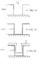
- FIGS. 1A-Cillustrate common problems associated with conventional via fabrication processes, when smaller feature sizes (e.g., 45 nanometer (nm) node or smaller technology) are involved.
- dielectric layer 120is deposited over substrate 100 , and via 101 is etched into dielectric layer 120 .
- via 101 /surface of dielectric 120are lined with diffusion barrier layer 130 .
- the diffusion barrier layercan be tantalum nitride (TaN), or any other suitable diffusion barrier material.
- Electroplatingis used to fill via 101 with copper (Cu). However, in order to perform the electroplating, it is first necessary to deposit a seed layer onto which the Cu can be subsequently plated. Namely, as shown in FIG. 1C , seed layer 140 is formed by sputter depositing Cu onto diffusion barrier layer 130 .
- a problem with this approachis that, as the via width shrinks to below about 80 nm and the aspect (depth/width) ratio becomes larger than about 5:1, the electroplating of the structure begins to fail.
- FIG. 1Cthere is a substantial non-uniformity of the Cu thickness in seed layer 140 .
- This non-uniformityis a consequence of the directional nature of the sputter deposition process coupled with the fact that a layer of Cu having a sufficient thickness so as to be continuous is required on the via bottom/sidewalls to ensure that there are no spots that cannot be plated.
- an excess amount of Cuis deposited on horizontal surfaces of the via. This excess Cu ends up overhanging the via opening.
- this overhangoccludes the via opening and causes the via opening to close off leaving an unfilled void within in the via, which is a catastrophic fault.
- a ruthenium (Ru) seed layeris deposited onto the diffusion barrier layer by chemical vapor deposition (CVD), i.e., from a ruthenium carbonyl (Ru 3 (CO) 12 ) precursor in the presence of excess CO.
- CVDchemical vapor deposition
- Ru 3 (CO) 12ruthenium carbonyl
- Ru seed layerhas significant drawbacks that arise from the relatively high resistivity of Ru compared to Cu and the chemical inertness of Ru.
- CMPchemical-mechanical polishing
- five nmis an approximate upper limit for the amount of Ru which can be polished away using a standard Cu polishing slurry.
- the bulk resistivity of Ruis more than four times higher than that of Cu. If only five nm of Ru are deposited, the resistivity of the resulting structure renders electroplating extremely difficult, as voltage drops across the wafer cause unacceptable non-uniformity in the Cu deposition.
- the present inventionprovides improved high aspect ratio vias and techniques for the formation thereof.
- a method of fabricating a copper plated high aspect ratio viacomprises the following steps.
- a high aspect ratio viais etched in a dielectric layer.
- a diffusion barrier layeris deposited into the high aspect ratio via and over one or more surfaces of the dielectric layer.
- a copper layeris deposited over the diffusion barrier layer.
- a ruthenium layeris deposited over the copper layer.
- the high aspect ratio viais filled with copper plated onto the ruthenium layer.
- a copper plated high aspect ratio via formed in a dielectric layercomprises a high aspect ratio via; a diffusion barrier layer lining the high aspect ratio via and one or more surfaces of the dielectric layer; a copper layer over the diffusion barrier layer; a ruthenium layer over the copper layer; and copper plated onto the ruthenium layer filling the high aspect ratio via to form the copper plated high aspect ratio via.
- FIGS. 1A-Care cross-sectional diagrams illustrating a conventional via fabrication process
- FIGS. 2A-Dare cross-sectional diagrams illustrating an exemplary via fabrication process according to an embodiment of the present invention.
- FIGS. 2A-Dare cross-sectional diagrams illustrating an exemplary via fabrication process.
- dielectric layer 220is deposited over substrate 200 .
- Dielectric layer 220can comprise any suitable dielectric material, including, but not limited to, one or more of silicon dioxide (SiO 2 ), silicon-carbon-oxygen-hydrogen materials (e.g., SICOH) and organic polymers, and can be deposited using any suitable deposition process, such as chemical vapor deposition (CVD), atomic layer deposition (ALD), evaporation, sputtering or solution based techniques, such as spin-on coating, to a thickness of from about 10 nanometers (nm) to about 1,000 nm.
- CVDchemical vapor deposition
- ALDatomic layer deposition
- evaporationevaporation
- sputteringevaporation
- solution based techniquessuch as spin-on coating
- Substrate 200generally represents any wiring or contact layer in a single or multilayer wiring array.
- High aspect ratio via 201is then etched into dielectric layer 220 , using any suitable etching process, such as reactive ion etching (RIE).
- RIEreactive ion etching
- high aspect ratio via 201is etched into dielectric layer 220 using RIE and has a depth d/width w aspect ratio of greater than or equal to about 5:1.
- diffusion barrier layer 230lines high aspect ratio via 201 /a top surface of dielectric layer 220 .
- Diffusion barrier layer 230can comprise any suitable diffusion barrier material, including, but not limited to, tantalum nitride (TaN), or other metal nitride, oxide, sulfide, boride or phosphide, and can be deposited in high aspect ratio via 201 /over a top surface of dielectric layer 220 using any suitable deposition process, such as CVD, ALD or sputtering, to a thickness of from about 0.5 nm to about 10 nm.
- TaNtantalum nitride
- ALDatomic layer
- Cu seed layer 240is deposited over diffusion barrier layer 230 .
- Cu seed layer 240can be deposited using any suitable deposition process, such as CVD, ALD or sputtering, to a thickness of from about one nm to about five nm.
- Cu seed layer 240is deposited primarily as a current carrying layer during electroplating, and thus (e.g., as compared the process presented in FIGS. 1A-C , described above) does not need to be of a thickness required for continuous coverage on the via sidewalls (i.e., Cu seed layer 240 only needs to be of a thickness required to serve as a current carrying layer during electroplating, see exemplary thicknesses provided immediately above). Therefore, overhang (described above) is not present (preventing occlusion and unfilled voids) which facilitates the extendibility of plating to smaller, higher aspect ratio structures.
- Ruthenium (Ru) seed layer 250is then deposited over Cu seed layer 240 .
- Ru seed layer 250can be deposited using any suitable deposition process, such as CVD or ALD.
- Ru seed layer 250is deposited using CVD, i.e., from a ruthenium carbonyl (Ru 3 (CO) 12 ) precursor in the presence of excess CO.
- Ru seed layer 250 formed by this highly conformal processis deposited only to a thickness that ensures a continuous coverage on the via sidewalls, and is therefore within limits set by standard chemical-mechanical polishing (CMP) (see description of FIG. 2D , below).
- CMPchemical-mechanical polishing
- Ru seed layer 250is deposited to a thickness of less than or equal to about five nm.
- Ru seed layer 250 over Cu seed layer 240is also referred to herein as a Ru-on-Cu bilayer.
- high aspect ratio via 201is filled with Cu 260 , for example, by electroplating Cu 260 onto Ru seed layer 250 , to form a Cu plated high aspect ratio via. If desired, CMP can then be used to plane plated Cu 260 /Ru seed layer 250 /Cu seed layer 240 /diffusion barrier layer 230 down to a top surface of dielectric layer 220 (not shown).
- One advantage of the present Ru-on-Cu bilayer seed layer configurationis that Cu plated onto Ru exhibits a superior morphology, for example, as compared to Cu plated on a Cu seed layer. Namely, in the lines, larger grains are observed, and in the via, both larger and oriented columnar grains are found. The larger grains improve conductivity, thus improving performance of the vias.
- both Ru-on-Cu and Cu-on-Ru seed layerswere produced on identical via structures, with one nm of Ru on three nm of Cu and with three nm of Cu on one nm of Ru, respectively.
- the Ru-on-Cu sampleplated successfully (i.e., uniform plating) while the Cu-on-Ru sample did not.
- the plating of the Cu-on-Ru sampleshowed the type of gross non-uniformity associated with insufficient conductivity of a substrate.
- the difference in the samplesmay be due to differing degrees of oxidation that the two seed layers incurred upon exposure to the atmosphere.
- Rua noble metal
- Cuis much less susceptible to oxidation than Cu.
- the Cuis protected from oxidation by the Ru layer thereover, while in the Cu-on-Ru structure the Cu is directly exposed to the atmosphere.
- the oxidation of the Cudecreases the conductivity of the Cu-on-Ru seed layer making plating more difficult. It is also possible that significant dissolution of Cu oxide may occur in a plating bath, with similar deleterious consequences for the substrate conductivity.
- Ru-on-Cu bilayer configurationis that, when diffusion barrier layer 230 comprises TaN (see above), a Cu/TaN interface results (i.e., between the Ru-on-Cu bilayer seed layer and the diffusion barrier layer).
- the Cu/TaN interfacehas been extensively tested and routinely employed in conventional systems.
Landscapes
- Engineering & Computer Science (AREA)
- Physics & Mathematics (AREA)
- Condensed Matter Physics & Semiconductors (AREA)
- General Physics & Mathematics (AREA)
- Computer Hardware Design (AREA)
- Microelectronics & Electronic Packaging (AREA)
- Power Engineering (AREA)
- Manufacturing & Machinery (AREA)
- Internal Circuitry In Semiconductor Integrated Circuit Devices (AREA)
- Drying Of Semiconductors (AREA)
- Other Surface Treatments For Metallic Materials (AREA)
- Electrodes Of Semiconductors (AREA)
Abstract
Description
- The present invention relates to semiconductor interconnect structures and more particularly, to improved high aspect ratio vias and techniques for the formation thereof.
- As the dimensions of multilayer wiring array features continue to shrink, the fabrication of vias is becoming increasingly more difficult. Namely, conventional via fabrication processes are unable to keep up with currently desirable scaled feature sizes.
FIGS. 1A-C , for example, illustrate common problems associated with conventional via fabrication processes, when smaller feature sizes (e.g., 45 nanometer (nm) node or smaller technology) are involved. As shown inFIG. 1A ,dielectric layer 120 is deposited oversubstrate 100, and via101 is etched intodielectric layer 120. As shown inFIG. 1B , via101/surface of dielectric120 are lined withdiffusion barrier layer 130. The diffusion barrier layer can be tantalum nitride (TaN), or any other suitable diffusion barrier material. Electroplating is used to fill via101 with copper (Cu). However, in order to perform the electroplating, it is first necessary to deposit a seed layer onto which the Cu can be subsequently plated. Namely, as shown inFIG. 1C ,seed layer 140 is formed by sputter depositing Cu ontodiffusion barrier layer 130. - A problem with this approach is that, as the via width shrinks to below about 80 nm and the aspect (depth/width) ratio becomes larger than about 5:1, the electroplating of the structure begins to fail. As shown in
FIG. 1C , there is a substantial non-uniformity of the Cu thickness inseed layer 140. This non-uniformity is a consequence of the directional nature of the sputter deposition process coupled with the fact that a layer of Cu having a sufficient thickness so as to be continuous is required on the via bottom/sidewalls to ensure that there are no spots that cannot be plated. As a result, an excess amount of Cu is deposited on horizontal surfaces of the via. This excess Cu ends up overhanging the via opening. As a result, when electroplating is attempted this overhang occludes the via opening and causes the via opening to close off leaving an unfilled void within in the via, which is a catastrophic fault. - In an attempt to prevent the above-described overhang occlusion problem, an alternative approach has been devised where instead of sputter depositing a Cu seed layer onto the diffusion barrier layer, a ruthenium (Ru) seed layer is deposited onto the diffusion barrier layer by chemical vapor deposition (CVD), i.e., from a ruthenium carbonyl (Ru3(CO)12) precursor in the presence of excess CO. A Ru seed layer produced in this manner can be conformally deposited and thus does not create a thick overhanging layer, which greatly reduces the problem of void formation in the subsequent Cu electroplating step.
- Use of a Ru seed layer, however, has significant drawbacks that arise from the relatively high resistivity of Ru compared to Cu and the chemical inertness of Ru. For example, following electroplating chemical-mechanical polishing (CMP) is typically used to plane the via metal down to the dielectric surface. As a practical matter, five nm is an approximate upper limit for the amount of Ru which can be polished away using a standard Cu polishing slurry. However, the bulk resistivity of Ru is more than four times higher than that of Cu. If only five nm of Ru are deposited, the resistivity of the resulting structure renders electroplating extremely difficult, as voltage drops across the wafer cause unacceptable non-uniformity in the Cu deposition. One could increase the conductivity of the substrate by depositing a thicker layer of Ru, and alleviate this problem, but then the subsequent CMP process would not be possible. One is left with a choice of problems, if the Ru is thick enough to make plating easy, subsequent CMP is not possible with the standard Cu polishing slurry. If the Ru layer is thinned to the point where CMP becomes possible, the substrate is too resistive for uniform plating using standard techniques. Furthermore, even if a method is developed to polish thicker layers of Ru, it would not be a desirable solution. The additional Ru added to facilitate the electroplating process would remain in the vias after CMP, which would reduce the volume available in the vias for Cu, and the resistance of the vias would be significantly increased, degrading performance.
- Thus, improved via fabrication processes are needed that can accommodate the most current scaled technology requirements and can consistently produce properly functioning, viable vias.
- The present invention provides improved high aspect ratio vias and techniques for the formation thereof. In one aspect of the invention, a method of fabricating a copper plated high aspect ratio via is provided. The method comprises the following steps. A high aspect ratio via is etched in a dielectric layer. A diffusion barrier layer is deposited into the high aspect ratio via and over one or more surfaces of the dielectric layer. A copper layer is deposited over the diffusion barrier layer. A ruthenium layer is deposited over the copper layer. The high aspect ratio via is filled with copper plated onto the ruthenium layer.
- In another aspect of the invention, a copper plated high aspect ratio via formed in a dielectric layer is provided. The copper plated high aspect ratio via comprises a high aspect ratio via; a diffusion barrier layer lining the high aspect ratio via and one or more surfaces of the dielectric layer; a copper layer over the diffusion barrier layer; a ruthenium layer over the copper layer; and copper plated onto the ruthenium layer filling the high aspect ratio via to form the copper plated high aspect ratio via.
- A more complete understanding of the present invention, as well as further features and advantages of the present invention, will be obtained by reference to the following detailed description and drawings.
FIGS. 1A-C are cross-sectional diagrams illustrating a conventional via fabrication process; andFIGS. 2A-D are cross-sectional diagrams illustrating an exemplary via fabrication process according to an embodiment of the present invention.FIGS. 2A-D are cross-sectional diagrams illustrating an exemplary via fabrication process. As shown inFIG. 2A ,dielectric layer 220 is deposited oversubstrate 200.Dielectric layer 220 can comprise any suitable dielectric material, including, but not limited to, one or more of silicon dioxide (SiO2), silicon-carbon-oxygen-hydrogen materials (e.g., SICOH) and organic polymers, and can be deposited using any suitable deposition process, such as chemical vapor deposition (CVD), atomic layer deposition (ALD), evaporation, sputtering or solution based techniques, such as spin-on coating, to a thickness of from about 10 nanometers (nm) to about 1,000 nm.Substrate 200 generally represents any wiring or contact layer in a single or multilayer wiring array. High aspect ratio via201 is then etched intodielectric layer 220, using any suitable etching process, such as reactive ion etching (RIE). According to one exemplary embodiment, high aspect ratio via201 is etched intodielectric layer 220 using RIE and has a depth d/width w aspect ratio of greater than or equal to about 5:1.- As shown in
FIG. 2B ,diffusion barrier layer 230 lines high aspect ratio via201/a top surface ofdielectric layer 220.Diffusion barrier layer 230 can comprise any suitable diffusion barrier material, including, but not limited to, tantalum nitride (TaN), or other metal nitride, oxide, sulfide, boride or phosphide, and can be deposited in high aspect ratio via201/over a top surface ofdielectric layer 220 using any suitable deposition process, such as CVD, ALD or sputtering, to a thickness of from about 0.5 nm to about 10 nm. - As shown in
FIG. 2C , copper (Cu)seed layer 240 is deposited overdiffusion barrier layer 230.Cu seed layer 240 can be deposited using any suitable deposition process, such as CVD, ALD or sputtering, to a thickness of from about one nm to about five nm.Cu seed layer 240 is deposited primarily as a current carrying layer during electroplating, and thus (e.g., as compared the process presented inFIGS. 1A-C , described above) does not need to be of a thickness required for continuous coverage on the via sidewalls (i.e.,Cu seed layer 240 only needs to be of a thickness required to serve as a current carrying layer during electroplating, see exemplary thicknesses provided immediately above). Therefore, overhang (described above) is not present (preventing occlusion and unfilled voids) which facilitates the extendibility of plating to smaller, higher aspect ratio structures. - Ruthenium (Ru) seed layer250 is then deposited over
Cu seed layer 240. Ru seed layer250 can be deposited using any suitable deposition process, such as CVD or ALD. According to an exemplary embodiment, Ru seed layer250 is deposited using CVD, i.e., from a ruthenium carbonyl (Ru3(CO)12) precursor in the presence of excess CO. Advantageously, Ru seed layer250 formed by this highly conformal process is deposited only to a thickness that ensures a continuous coverage on the via sidewalls, and is therefore within limits set by standard chemical-mechanical polishing (CMP) (see description ofFIG. 2D , below). According to an exemplary embodiment, Ru seed layer250 is deposited to a thickness of less than or equal to about five nm. Ru seed layer250 overCu seed layer 240 is also referred to herein as a Ru-on-Cu bilayer. - As shown in
FIG. 2D , high aspect ratio via201 is filled withCu 260, for example, by electroplatingCu 260 onto Ru seed layer250, to form a Cu plated high aspect ratio via. If desired, CMP can then be used to plane platedCu 260/Ru seed layer250/Cu seed layer 240/diffusion barrier layer 230 down to a top surface of dielectric layer220 (not shown). - One advantage of the present Ru-on-Cu bilayer seed layer configuration (for Cu electroplating, see above) is that Cu plated onto Ru exhibits a superior morphology, for example, as compared to Cu plated on a Cu seed layer. Namely, in the lines, larger grains are observed, and in the via, both larger and oriented columnar grains are found. The larger grains improve conductivity, thus improving performance of the vias.
- Prior via fabrication techniques also involving a bilayer seed layer employed a Cu-on-Ru configuration. This Cu-on-Ru configuration, however, has several notable disadvantages over the present Ru-on-Cu bilayer configuration. Namely, the Cu-on-Ru configuration does not provide the morphology advantages associated with Cu plating onto Ru, as described above. Further, with the present Ru-on-Cu bilayer configuration, the Cu component of the bilayer can be made thinner than in a Cu-on-Ru configuration, and still remain viable for plating.
- By way of example only, both Ru-on-Cu and Cu-on-Ru seed layers were produced on identical via structures, with one nm of Ru on three nm of Cu and with three nm of Cu on one nm of Ru, respectively. Using identical plating conditions it was found that the Ru-on-Cu sample plated successfully (i.e., uniform plating) while the Cu-on-Ru sample did not. The plating of the Cu-on-Ru sample showed the type of gross non-uniformity associated with insufficient conductivity of a substrate.
- The difference in the samples may be due to differing degrees of oxidation that the two seed layers incurred upon exposure to the atmosphere. Ru, a noble metal, is much less susceptible to oxidation than Cu. In the Ru-on-Cu structure the Cu is protected from oxidation by the Ru layer thereover, while in the Cu-on-Ru structure the Cu is directly exposed to the atmosphere. The oxidation of the Cu decreases the conductivity of the Cu-on-Ru seed layer making plating more difficult. It is also possible that significant dissolution of Cu oxide may occur in a plating bath, with similar deleterious consequences for the substrate conductivity.
- Another advantage of the Ru-on-Cu bilayer configuration is that, when
diffusion barrier layer 230 comprises TaN (see above), a Cu/TaN interface results (i.e., between the Ru-on-Cu bilayer seed layer and the diffusion barrier layer). The Cu/TaN interface has been extensively tested and routinely employed in conventional systems. - Although illustrative embodiments of the present invention have been described herein, it is to be understood that the invention is not limited to those precise embodiments, and that various other changes and modifications may be made by one skilled in the art without departing from the scope of the invention.
Claims (18)
Priority Applications (5)
| Application Number | Priority Date | Filing Date | Title |
|---|---|---|---|
| US12/163,172US7964497B2 (en) | 2008-06-27 | 2008-06-27 | Structure to facilitate plating into high aspect ratio vias |
| EP08166587AEP2139034A1 (en) | 2008-06-27 | 2008-10-14 | Structure to facilitate plating into high aspect ratio vias and method of its fabrication |
| JP2008268013AJP4536809B2 (en) | 2008-06-27 | 2008-10-16 | Copper plated high aspect ratio vias and methods of manufacturing the same |
| CN200910150840ACN101615591A (en) | 2008-06-27 | 2009-06-23 | Copper plated high aspect ratio through holes and manufacture method thereof |
| TW098121240ATW201017821A (en) | 2008-06-27 | 2009-06-24 | Structure to facilitate plating into high aspect ratio vias |
Applications Claiming Priority (1)
| Application Number | Priority Date | Filing Date | Title |
|---|---|---|---|
| US12/163,172US7964497B2 (en) | 2008-06-27 | 2008-06-27 | Structure to facilitate plating into high aspect ratio vias |
Publications (2)
| Publication Number | Publication Date |
|---|---|
| US20090321933A1true US20090321933A1 (en) | 2009-12-31 |
| US7964497B2 US7964497B2 (en) | 2011-06-21 |
Family
ID=40635481
Family Applications (1)
| Application Number | Title | Priority Date | Filing Date |
|---|---|---|---|
| US12/163,172Expired - Fee RelatedUS7964497B2 (en) | 2008-06-27 | 2008-06-27 | Structure to facilitate plating into high aspect ratio vias |
Country Status (5)
| Country | Link |
|---|---|
| US (1) | US7964497B2 (en) |
| EP (1) | EP2139034A1 (en) |
| JP (1) | JP4536809B2 (en) |
| CN (1) | CN101615591A (en) |
| TW (1) | TW201017821A (en) |
Cited By (2)
| Publication number | Priority date | Publication date | Assignee | Title |
|---|---|---|---|---|
| US8661664B2 (en) | 2010-07-19 | 2014-03-04 | International Business Machines Corporation | Techniques for forming narrow copper filled vias having improved conductivity |
| US9748173B1 (en)* | 2016-07-06 | 2017-08-29 | International Business Machines Corporation | Hybrid interconnects and method of forming the same |
Families Citing this family (3)
| Publication number | Priority date | Publication date | Assignee | Title |
|---|---|---|---|---|
| US10847463B2 (en)* | 2017-08-22 | 2020-11-24 | Applied Materials, Inc. | Seed layers for copper interconnects |
| US12322649B2 (en) | 2020-09-11 | 2025-06-03 | Taiwan Semiconductor Manufacturing Co., Ltd. | Interconnect structure of semiconductor device |
| US11527476B2 (en)* | 2020-09-11 | 2022-12-13 | Taiwan Semiconductor Manufacturing Co., Ltd. | Interconnect structure of semiconductor device |
Citations (17)
| Publication number | Priority date | Publication date | Assignee | Title |
|---|---|---|---|---|
| US6069073A (en)* | 1997-09-18 | 2000-05-30 | Electronics And Telecommunications Research Institute | Method for forming diffusion barrier layers |
| US20010033023A1 (en)* | 2000-03-28 | 2001-10-25 | Kabushiki Kaisha Toshiba | Semiconductor device and method of manufacturing the same |
| US6403491B1 (en)* | 2000-11-01 | 2002-06-11 | Applied Materials, Inc. | Etch method using a dielectric etch chamber with expanded process window |
| US20040135255A1 (en)* | 2003-01-09 | 2004-07-15 | Noriaki Matsunaga | Semiconductor device and its manufacturing method |
| US20040175921A1 (en)* | 2003-03-04 | 2004-09-09 | Infineon Technologies North America Corp. | Reduction of the shear stress in copper via's in organic interlayer dielectric material |
| US6790773B1 (en)* | 2002-08-28 | 2004-09-14 | Novellus Systems, Inc. | Process for forming barrier/seed structures for integrated circuits |
| US20050095846A1 (en)* | 2003-10-31 | 2005-05-05 | Basol Bulent M. | System and method for defect free conductor deposition on substrates |
| US20050181598A1 (en)* | 2003-01-15 | 2005-08-18 | Kailasam Sridhar K. | Methods of providing an adhesion layer for adhesion of barrier and/or seed layers to dielectric films |
| US6989599B1 (en)* | 1998-02-23 | 2006-01-24 | Hitachi, Ltd. | Semiconductor device with layered interconnect structure |
| US20060121733A1 (en)* | 2004-10-26 | 2006-06-08 | Kilpela Olli V | Selective formation of metal layers in an integrated circuit |
| US20060193372A1 (en)* | 2000-10-10 | 2006-08-31 | Fujitsu Limited | System and method for generating shaped ultrawide bandwidth wavelets |
| US20060199372A1 (en)* | 2005-03-01 | 2006-09-07 | Applied Materials, Inc. | Reduction of copper dewetting by transition metal deposition |
| US20070062817A1 (en)* | 2005-09-20 | 2007-03-22 | Alchimer | Method of coating a surface of a substrate with a metal by electroplating |
| US20070190780A1 (en)* | 2003-06-18 | 2007-08-16 | Applied Materials, Inc. | Atomic layer deposition of barrier materials |
| US20070205510A1 (en)* | 2006-03-03 | 2007-09-06 | Lavoie Adrien R | Noble metal barrier layers |
| US20070238288A1 (en)* | 2006-03-29 | 2007-10-11 | Tokyo Electron Limited | Method for integrating a conformal ruthenium layer into copper metallization of high aspect ratio features |
| US20070273042A1 (en)* | 2006-03-30 | 2007-11-29 | Kuhn Kelin J | Copper-filled trench contact for transistor performance improvement |
Family Cites Families (5)
| Publication number | Priority date | Publication date | Assignee | Title |
|---|---|---|---|---|
| JP2002075994A (en) | 2000-08-24 | 2002-03-15 | Matsushita Electric Ind Co Ltd | Semiconductor device and manufacturing method thereof |
| US7279421B2 (en) | 2004-11-23 | 2007-10-09 | Tokyo Electron Limited | Method and deposition system for increasing deposition rates of metal layers from metal-carbonyl precursors |
| US8435351B2 (en) | 2004-11-29 | 2013-05-07 | Tokyo Electron Limited | Method and system for measuring a flow rate in a solid precursor delivery system |
| US7396766B2 (en) | 2005-03-31 | 2008-07-08 | Tokyo Electron Limited | Low-temperature chemical vapor deposition of low-resistivity ruthenium layers |
| JP2008041700A (en) | 2006-08-01 | 2008-02-21 | Tokyo Electron Ltd | Method and apparatus of forming film, and recording medium |
- 2008
- 2008-06-27USUS12/163,172patent/US7964497B2/ennot_activeExpired - Fee Related
- 2008-10-14EPEP08166587Apatent/EP2139034A1/ennot_activeWithdrawn
- 2008-10-16JPJP2008268013Apatent/JP4536809B2/ennot_activeExpired - Fee Related
- 2009
- 2009-06-23CNCN200910150840Apatent/CN101615591A/enactivePending
- 2009-06-24TWTW098121240Apatent/TW201017821A/enunknown
Patent Citations (18)
| Publication number | Priority date | Publication date | Assignee | Title |
|---|---|---|---|---|
| US6069073A (en)* | 1997-09-18 | 2000-05-30 | Electronics And Telecommunications Research Institute | Method for forming diffusion barrier layers |
| US7253103B2 (en)* | 1998-02-23 | 2007-08-07 | Hitachi, Ltd. | Method for producing semiconductor devices that includes forming a copper film in contact with a ruthenium film |
| US6989599B1 (en)* | 1998-02-23 | 2006-01-24 | Hitachi, Ltd. | Semiconductor device with layered interconnect structure |
| US20010033023A1 (en)* | 2000-03-28 | 2001-10-25 | Kabushiki Kaisha Toshiba | Semiconductor device and method of manufacturing the same |
| US20060193372A1 (en)* | 2000-10-10 | 2006-08-31 | Fujitsu Limited | System and method for generating shaped ultrawide bandwidth wavelets |
| US6403491B1 (en)* | 2000-11-01 | 2002-06-11 | Applied Materials, Inc. | Etch method using a dielectric etch chamber with expanded process window |
| US6790773B1 (en)* | 2002-08-28 | 2004-09-14 | Novellus Systems, Inc. | Process for forming barrier/seed structures for integrated circuits |
| US20040135255A1 (en)* | 2003-01-09 | 2004-07-15 | Noriaki Matsunaga | Semiconductor device and its manufacturing method |
| US20050181598A1 (en)* | 2003-01-15 | 2005-08-18 | Kailasam Sridhar K. | Methods of providing an adhesion layer for adhesion of barrier and/or seed layers to dielectric films |
| US20040175921A1 (en)* | 2003-03-04 | 2004-09-09 | Infineon Technologies North America Corp. | Reduction of the shear stress in copper via's in organic interlayer dielectric material |
| US20070190780A1 (en)* | 2003-06-18 | 2007-08-16 | Applied Materials, Inc. | Atomic layer deposition of barrier materials |
| US20050095846A1 (en)* | 2003-10-31 | 2005-05-05 | Basol Bulent M. | System and method for defect free conductor deposition on substrates |
| US20060121733A1 (en)* | 2004-10-26 | 2006-06-08 | Kilpela Olli V | Selective formation of metal layers in an integrated circuit |
| US20060199372A1 (en)* | 2005-03-01 | 2006-09-07 | Applied Materials, Inc. | Reduction of copper dewetting by transition metal deposition |
| US20070062817A1 (en)* | 2005-09-20 | 2007-03-22 | Alchimer | Method of coating a surface of a substrate with a metal by electroplating |
| US20070205510A1 (en)* | 2006-03-03 | 2007-09-06 | Lavoie Adrien R | Noble metal barrier layers |
| US20070238288A1 (en)* | 2006-03-29 | 2007-10-11 | Tokyo Electron Limited | Method for integrating a conformal ruthenium layer into copper metallization of high aspect ratio features |
| US20070273042A1 (en)* | 2006-03-30 | 2007-11-29 | Kuhn Kelin J | Copper-filled trench contact for transistor performance improvement |
Cited By (4)
| Publication number | Priority date | Publication date | Assignee | Title |
|---|---|---|---|---|
| US8661664B2 (en) | 2010-07-19 | 2014-03-04 | International Business Machines Corporation | Techniques for forming narrow copper filled vias having improved conductivity |
| US9392690B2 (en) | 2010-07-19 | 2016-07-12 | Globalfoundries Inc. | Method and structure to improve the conductivity of narrow copper filled vias |
| US9748173B1 (en)* | 2016-07-06 | 2017-08-29 | International Business Machines Corporation | Hybrid interconnects and method of forming the same |
| US10446491B2 (en) | 2016-07-06 | 2019-10-15 | International Business Machines Corporation | Hybrid interconnects and method of forming the same |
Also Published As
| Publication number | Publication date |
|---|---|
| CN101615591A (en) | 2009-12-30 |
| TW201017821A (en) | 2010-05-01 |
| JP4536809B2 (en) | 2010-09-01 |
| US7964497B2 (en) | 2011-06-21 |
| EP2139034A1 (en) | 2009-12-30 |
| JP2010010642A (en) | 2010-01-14 |
Similar Documents
| Publication | Publication Date | Title |
|---|---|---|
| US10256186B2 (en) | Interconnect structure having subtractive etch feature and damascene feature | |
| KR0128264B1 (en) | Method of forming semiconductor devices, liners and metal wires and vias | |
| US7915162B2 (en) | Method of forming damascene filament wires | |
| US7521358B2 (en) | Process integration scheme to lower overall dielectric constant in BEoL interconnect structures | |
| JP4049978B2 (en) | Metal wiring formation method using plating | |
| US20100314765A1 (en) | Interconnection structure of semiconductor integrated circuit and method for making the same | |
| TWI753993B (en) | Interconnect structure and method of forming the same | |
| US20200035906A1 (en) | Mtj bottom metal via in a memory cell and method for producing the same | |
| KR100790452B1 (en) | Multi-layer metallization method of semiconductor device using damascene process | |
| US7964497B2 (en) | Structure to facilitate plating into high aspect ratio vias | |
| KR20250091322A (en) | Ruthenium liner and cap for back-end-of-line applications | |
| TW202510205A (en) | Methods for making semiconductor devices that include metal cap layers | |
| US10825720B2 (en) | Single trench damascene interconnect using TiN HMO | |
| US12266607B2 (en) | Bottom barrier free interconnects without voids | |
| CN113380763A (en) | Copper interconnection structure and preparation method thereof | |
| US20040256733A1 (en) | Method for manufacturing a semiconductor device and a semiconductor device | |
| JP2022548081A (en) | Trapezoidal interconnect with tight BEOL pitch | |
| CN1617323A (en) | Method for forming metal wire in semiconductor device | |
| WO2012041033A1 (en) | Method for forming metal interconnection structure, through hole between metallization layers and interconnect metallization lines | |
| TWI621234B (en) | Method of forming interconnect structure | |
| KR20070052452A (en) | Method for manufacturing metal wiring of semiconductor device | |
| CN110890317A (en) | Semiconductor device and method for manufacturing the same | |
| JP2004014816A (en) | Semiconductor manufacturing method and semiconductor device |
Legal Events
| Date | Code | Title | Description |
|---|---|---|---|
| AS | Assignment | Owner name:INTERNATIONAL BUSINESS MACHINES CORPORATION, NEW Y Free format text:ASSIGNMENT OF ASSIGNORS INTEREST;ASSIGNORS:MCFEELY, FENTON R.;YANG, CHIH-CHAO;REEL/FRAME:021671/0223;SIGNING DATES FROM 20080624 TO 20080625 Owner name:INTERNATIONAL BUSINESS MACHINES CORPORATION, NEW Y Free format text:ASSIGNMENT OF ASSIGNORS INTEREST;ASSIGNORS:MCFEELY, FENTON R.;YANG, CHIH-CHAO;SIGNING DATES FROM 20080624 TO 20080625;REEL/FRAME:021671/0223 | |
| STCF | Information on status: patent grant | Free format text:PATENTED CASE | |
| REMI | Maintenance fee reminder mailed | ||
| FPAY | Fee payment | Year of fee payment:4 | |
| SULP | Surcharge for late payment | ||
| AS | Assignment | Owner name:GLOBALFOUNDRIES U.S. 2 LLC, NEW YORK Free format text:ASSIGNMENT OF ASSIGNORS INTEREST;ASSIGNOR:INTERNATIONAL BUSINESS MACHINES CORPORATION;REEL/FRAME:036550/0001 Effective date:20150629 | |
| AS | Assignment | Owner name:GLOBALFOUNDRIES INC., CAYMAN ISLANDS Free format text:ASSIGNMENT OF ASSIGNORS INTEREST;ASSIGNORS:GLOBALFOUNDRIES U.S. 2 LLC;GLOBALFOUNDRIES U.S. INC.;REEL/FRAME:036779/0001 Effective date:20150910 | |
| AS | Assignment | Owner name:WILMINGTON TRUST, NATIONAL ASSOCIATION, DELAWARE Free format text:SECURITY AGREEMENT;ASSIGNOR:GLOBALFOUNDRIES INC.;REEL/FRAME:049490/0001 Effective date:20181127 | |
| MAFP | Maintenance fee payment | Free format text:PAYMENT OF MAINTENANCE FEE, 8TH YEAR, LARGE ENTITY (ORIGINAL EVENT CODE: M1552); ENTITY STATUS OF PATENT OWNER: LARGE ENTITY Year of fee payment:8 | |
| AS | Assignment | Owner name:GLOBALFOUNDRIES INC., CAYMAN ISLANDS Free format text:RELEASE BY SECURED PARTY;ASSIGNOR:WILMINGTON TRUST, NATIONAL ASSOCIATION;REEL/FRAME:054479/0842 Effective date:20200410 Owner name:TAIWAN SEMICONDUCTOR MANUFACTURING CO., LTD., TAIWAN Free format text:ASSIGNMENT OF ASSIGNORS INTEREST;ASSIGNOR:GLOBALFOUNDRIES INC.;REEL/FRAME:054482/0862 Effective date:20200515 | |
| AS | Assignment | Owner name:GLOBALFOUNDRIES INC., CAYMAN ISLANDS Free format text:RELEASE BY SECURED PARTY;ASSIGNOR:WILMINGTON TRUST, NATIONAL ASSOCIATION;REEL/FRAME:054636/0001 Effective date:20201117 | |
| FEPP | Fee payment procedure | Free format text:MAINTENANCE FEE REMINDER MAILED (ORIGINAL EVENT CODE: REM.); ENTITY STATUS OF PATENT OWNER: LARGE ENTITY | |
| LAPS | Lapse for failure to pay maintenance fees | Free format text:PATENT EXPIRED FOR FAILURE TO PAY MAINTENANCE FEES (ORIGINAL EVENT CODE: EXP.); ENTITY STATUS OF PATENT OWNER: LARGE ENTITY | |
| STCH | Information on status: patent discontinuation | Free format text:PATENT EXPIRED DUE TO NONPAYMENT OF MAINTENANCE FEES UNDER 37 CFR 1.362 | |
| FP | Lapsed due to failure to pay maintenance fee | Effective date:20230621 |