US20090321853A1 - HIGH-k/METAL GATE MOSFET WITH REDUCED PARASITIC CAPACITANCE - Google Patents
HIGH-k/METAL GATE MOSFET WITH REDUCED PARASITIC CAPACITANCEDownload PDFInfo
- Publication number
- US20090321853A1 US20090321853A1US12/554,292US55429209AUS2009321853A1US 20090321853 A1US20090321853 A1US 20090321853A1US 55429209 AUS55429209 AUS 55429209AUS 2009321853 A1US2009321853 A1US 2009321853A1
- Authority
- US
- United States
- Prior art keywords
- gate
- metal
- dielectric
- gate dielectric
- conductor
- Prior art date
- Legal status (The legal status is an assumption and is not a legal conclusion. Google has not performed a legal analysis and makes no representation as to the accuracy of the status listed.)
- Granted
Links
- 229910052751metalInorganic materials0.000titleclaimsabstractdescription131
- 239000002184metalSubstances0.000titleclaimsabstractdescription131
- 230000003071parasitic effectEffects0.000titleabstractdescription10
- 239000004020conductorSubstances0.000claimsabstractdescription106
- 239000004065semiconductorSubstances0.000claimsabstractdescription92
- 125000006850spacer groupChemical group0.000claimsabstractdescription81
- 239000000758substrateSubstances0.000claimsabstractdescription45
- 229910044991metal oxideInorganic materials0.000claimsabstractdescription11
- 150000004706metal oxidesChemical class0.000claimsabstractdescription11
- 230000005669field effectEffects0.000claimsabstractdescription9
- 239000003989dielectric materialSubstances0.000claimsdescription42
- 150000004767nitridesChemical class0.000claimsdescription9
- GWEVSGVZZGPLCZ-UHFFFAOYSA-NTitan oxideChemical compoundO=[Ti]=OGWEVSGVZZGPLCZ-UHFFFAOYSA-N0.000claimsdescription8
- MCMNRKCIXSYSNV-UHFFFAOYSA-NZirconium dioxideChemical compoundO=[Zr]=OMCMNRKCIXSYSNV-UHFFFAOYSA-N0.000claimsdescription8
- 229910021332silicideInorganic materials0.000claimsdescription7
- 239000011800void materialSubstances0.000claimsdescription7
- FVBUAEGBCNSCDD-UHFFFAOYSA-Nsilicide(4-)Chemical compound[Si-4]FVBUAEGBCNSCDD-UHFFFAOYSA-N0.000claimsdescription6
- MRELNEQAGSRDBK-UHFFFAOYSA-Nlanthanum oxideInorganic materials[O-2].[O-2].[O-2].[La+3].[La+3]MRELNEQAGSRDBK-UHFFFAOYSA-N0.000claimsdescription5
- KTUFCUMIWABKDW-UHFFFAOYSA-Noxo(oxolanthaniooxy)lanthanumChemical compoundO=[La]O[La]=OKTUFCUMIWABKDW-UHFFFAOYSA-N0.000claimsdescription5
- 229910045601alloyInorganic materials0.000claimsdescription4
- 239000000956alloySubstances0.000claimsdescription4
- PNEYBMLMFCGWSK-UHFFFAOYSA-Naluminium oxideInorganic materials[O-2].[O-2].[O-2].[Al+3].[Al+3]PNEYBMLMFCGWSK-UHFFFAOYSA-N0.000claimsdescription4
- 229910052593corundumInorganic materials0.000claimsdescription4
- CJNBYAVZURUTKZ-UHFFFAOYSA-Nhafnium(IV) oxideInorganic materialsO=[Hf]=OCJNBYAVZURUTKZ-UHFFFAOYSA-N0.000claimsdescription4
- PBCFLUZVCVVTBY-UHFFFAOYSA-Ntantalum pentoxideInorganic materialsO=[Ta](=O)O[Ta](=O)=OPBCFLUZVCVVTBY-UHFFFAOYSA-N0.000claimsdescription4
- 229910001845yogo sapphireInorganic materials0.000claimsdescription4
- BPQQTUXANYXVAA-UHFFFAOYSA-NOrthosilicateChemical compound[O-][Si]([O-])([O-])[O-]BPQQTUXANYXVAA-UHFFFAOYSA-N0.000claims3
- 238000000034methodMethods0.000description44
- 230000008569processEffects0.000description38
- 239000000463materialSubstances0.000description21
- 238000005229chemical vapour depositionMethods0.000description18
- 238000005530etchingMethods0.000description15
- 238000002955isolationMethods0.000description10
- 238000004518low pressure chemical vapour depositionMethods0.000description9
- 238000000623plasma-assisted chemical vapour depositionMethods0.000description9
- VYPSYNLAJGMNEJ-UHFFFAOYSA-NSilicium dioxideChemical compoundO=[Si]=OVYPSYNLAJGMNEJ-UHFFFAOYSA-N0.000description8
- 238000000231atomic layer depositionMethods0.000description8
- 238000000151depositionMethods0.000description8
- 230000008021depositionEffects0.000description8
- 238000005137deposition processMethods0.000description8
- 239000000126substanceSubstances0.000description8
- IJGRMHOSHXDMSA-UHFFFAOYSA-NAtomic nitrogenChemical compoundN#NIJGRMHOSHXDMSA-UHFFFAOYSA-N0.000description7
- 229910052581Si3N4Inorganic materials0.000description7
- 229910052710siliconInorganic materials0.000description7
- HQVNEWCFYHHQES-UHFFFAOYSA-Nsilicon nitrideChemical compoundN12[Si]34N5[Si]62N3[Si]51N64HQVNEWCFYHHQES-UHFFFAOYSA-N0.000description7
- 238000009792diffusion processMethods0.000description6
- 238000011049fillingMethods0.000description6
- 229910052760oxygenInorganic materials0.000description6
- XUIMIQQOPSSXEZ-UHFFFAOYSA-NSiliconChemical compound[Si]XUIMIQQOPSSXEZ-UHFFFAOYSA-N0.000description5
- 238000000224chemical solution depositionMethods0.000description5
- 230000003647oxidationEffects0.000description5
- 238000007254oxidation reactionMethods0.000description5
- 239000010703siliconSubstances0.000description5
- 230000015572biosynthetic processEffects0.000description4
- 238000001704evaporationMethods0.000description4
- 230000008020evaporationEffects0.000description4
- -1for exampleSubstances0.000description4
- 238000004519manufacturing processMethods0.000description4
- 229910052757nitrogenInorganic materials0.000description4
- 239000001301oxygenSubstances0.000description4
- 238000005240physical vapour depositionMethods0.000description4
- 238000001289rapid thermal chemical vapour depositionMethods0.000description4
- 229910052814silicon oxideInorganic materials0.000description4
- LYCAIKOWRPUZTN-UHFFFAOYSA-NEthylene glycolChemical compoundOCCOLYCAIKOWRPUZTN-UHFFFAOYSA-N0.000description3
- 229910000577Silicon-germaniumInorganic materials0.000description3
- QVGXLLKOCUKJST-UHFFFAOYSA-Natomic oxygenChemical compound[O]QVGXLLKOCUKJST-UHFFFAOYSA-N0.000description3
- 239000011248coating agentSubstances0.000description3
- 238000000576coating methodMethods0.000description3
- 238000001312dry etchingMethods0.000description3
- 230000000694effectsEffects0.000description3
- 238000001459lithographyMethods0.000description3
- 229920002120photoresistant polymerPolymers0.000description3
- 238000005498polishingMethods0.000description3
- 238000001039wet etchingMethods0.000description3
- QGZKDVFQNNGYKY-UHFFFAOYSA-NAmmoniaChemical compoundNQGZKDVFQNNGYKY-UHFFFAOYSA-N0.000description2
- RTZKZFJDLAIYFH-UHFFFAOYSA-NDiethyl etherChemical compoundCCOCCRTZKZFJDLAIYFH-UHFFFAOYSA-N0.000description2
- NBIIXXVUZAFLBC-UHFFFAOYSA-NPhosphoric acidChemical compoundOP(O)(O)=ONBIIXXVUZAFLBC-UHFFFAOYSA-N0.000description2
- 230000004913activationEffects0.000description2
- 229910052799carbonInorganic materials0.000description2
- 238000006243chemical reactionMethods0.000description2
- 238000000313electron-beam-induced depositionMethods0.000description2
- 238000000227grindingMethods0.000description2
- 229910052739hydrogenInorganic materials0.000description2
- 239000012212insulatorSubstances0.000description2
- 238000007737ion beam depositionMethods0.000description2
- 238000005468ion implantationMethods0.000description2
- 238000001451molecular beam epitaxyMethods0.000description2
- 238000001020plasma etchingMethods0.000description2
- 229920000412polyarylenePolymers0.000description2
- 229910021420polycrystalline siliconInorganic materials0.000description2
- 229920005591polysiliconPolymers0.000description2
- 235000012239silicon dioxideNutrition0.000description2
- 239000000377silicon dioxideSubstances0.000description2
- 238000005728strengtheningMethods0.000description2
- 238000000038ultrahigh vacuum chemical vapour depositionMethods0.000description2
- 229910018182Al—CuInorganic materials0.000description1
- 229910015844BCl3Inorganic materials0.000description1
- KRHYYFGTRYWZRS-UHFFFAOYSA-NFluoraneChemical compoundFKRHYYFGTRYWZRS-UHFFFAOYSA-N0.000description1
- 229910001218Gallium arsenideInorganic materials0.000description1
- 229910000673Indium arsenideInorganic materials0.000description1
- 229910018503SF6Inorganic materials0.000description1
- 229910003811SiGeCInorganic materials0.000description1
- NINIDFKCEFEMDL-UHFFFAOYSA-NSulfurChemical compound[S]NINIDFKCEFEMDL-UHFFFAOYSA-N0.000description1
- ATJFFYVFTNAWJD-UHFFFAOYSA-NTinChemical compound[Sn]ATJFFYVFTNAWJD-UHFFFAOYSA-N0.000description1
- LEVVHYCKPQWKOP-UHFFFAOYSA-N[Si].[Ge]Chemical compound[Si].[Ge]LEVVHYCKPQWKOP-UHFFFAOYSA-N0.000description1
- 229910052782aluminiumInorganic materials0.000description1
- 229910000147aluminium phosphateInorganic materials0.000description1
- 229910021529ammoniaInorganic materials0.000description1
- 125000003118aryl groupChemical group0.000description1
- 238000004380ashingMethods0.000description1
- 230000004888barrier functionEffects0.000description1
- 230000008901benefitEffects0.000description1
- 125000002915carbonyl groupChemical group[*:2]C([*:1])=O0.000description1
- 230000000295complement effectEffects0.000description1
- 150000001875compoundsChemical class0.000description1
- 229910052802copperInorganic materials0.000description1
- 230000003247decreasing effectEffects0.000description1
- 238000000280densificationMethods0.000description1
- 239000002019doping agentSubstances0.000description1
- 229910052733galliumInorganic materials0.000description1
- 229910052732germaniumInorganic materials0.000description1
- 229910052737goldInorganic materials0.000description1
- 229910052736halogenInorganic materials0.000description1
- RPQDHPTXJYYUPQ-UHFFFAOYSA-Nindium arsenideChemical compound[In]#[As]RPQDHPTXJYYUPQ-UHFFFAOYSA-N0.000description1
- 230000005527interface trapEffects0.000description1
- 238000010884ion-beam techniqueMethods0.000description1
- 229910052741iridiumInorganic materials0.000description1
- 125000005647linker groupChemical group0.000description1
- 150000002739metalsChemical class0.000description1
- 229910003455mixed metal oxideInorganic materials0.000description1
- 239000000203mixtureSubstances0.000description1
- 229910003465moissaniteInorganic materials0.000description1
- 238000000059patterningMethods0.000description1
- 238000007747platingMethods0.000description1
- 229910052697platinumInorganic materials0.000description1
- 230000005855radiationEffects0.000description1
- 229910052761rare earth metalInorganic materials0.000description1
- 150000002910rare earth metalsChemical class0.000description1
- 230000009467reductionEffects0.000description1
- 238000010405reoxidation reactionMethods0.000description1
- 229910052702rheniumInorganic materials0.000description1
- 229910052703rhodiumInorganic materials0.000description1
- 229910052707rutheniumInorganic materials0.000description1
- 239000005368silicate glassSubstances0.000description1
- 150000004760silicatesChemical class0.000description1
- 229910010271silicon carbideInorganic materials0.000description1
- 229910052709silverInorganic materials0.000description1
- 238000004544sputter depositionMethods0.000description1
- 230000000087stabilizing effectEffects0.000description1
- 150000003457sulfonesChemical class0.000description1
- 150000003462sulfoxidesChemical class0.000description1
- 229910052717sulfurInorganic materials0.000description1
- 239000011593sulfurSubstances0.000description1
- OBTWBSRJZRCYQV-UHFFFAOYSA-Nsulfuryl difluorideChemical compoundFS(F)(=O)=OOBTWBSRJZRCYQV-UHFFFAOYSA-N0.000description1
- 229920001187thermosetting polymerPolymers0.000description1
- FAQYAMRNWDIXMY-UHFFFAOYSA-NtrichloroboraneChemical compoundClB(Cl)ClFAQYAMRNWDIXMY-UHFFFAOYSA-N0.000description1
- 229910052721tungstenInorganic materials0.000description1
Images


Classifications
- H—ELECTRICITY
- H10—SEMICONDUCTOR DEVICES; ELECTRIC SOLID-STATE DEVICES NOT OTHERWISE PROVIDED FOR
- H10D—INORGANIC ELECTRIC SEMICONDUCTOR DEVICES
- H10D64/00—Electrodes of devices having potential barriers
- H10D64/60—Electrodes characterised by their materials
- H10D64/66—Electrodes having a conductor capacitively coupled to a semiconductor by an insulator, e.g. MIS electrodes
- H10D64/675—Gate sidewall spacers
- H10D64/679—Gate sidewall spacers comprising air gaps
- H—ELECTRICITY
- H10—SEMICONDUCTOR DEVICES; ELECTRIC SOLID-STATE DEVICES NOT OTHERWISE PROVIDED FOR
- H10D—INORGANIC ELECTRIC SEMICONDUCTOR DEVICES
- H10D30/00—Field-effect transistors [FET]
- H10D30/60—Insulated-gate field-effect transistors [IGFET]
- H10D30/601—Insulated-gate field-effect transistors [IGFET] having lightly-doped drain or source extensions, e.g. LDD IGFETs or DDD IGFETs
- H10D30/608—Insulated-gate field-effect transistors [IGFET] having lightly-doped drain or source extensions, e.g. LDD IGFETs or DDD IGFETs having non-planar bodies, e.g. having recessed gate electrodes
- H—ELECTRICITY
- H10—SEMICONDUCTOR DEVICES; ELECTRIC SOLID-STATE DEVICES NOT OTHERWISE PROVIDED FOR
- H10D—INORGANIC ELECTRIC SEMICONDUCTOR DEVICES
- H10D30/00—Field-effect transistors [FET]
- H10D30/01—Manufacture or treatment
- H10D30/021—Manufacture or treatment of FETs having insulated gates [IGFET]
- H10D30/0223—Manufacture or treatment of FETs having insulated gates [IGFET] having source and drain regions or source and drain extensions self-aligned to sides of the gate
- H10D30/0225—Manufacture or treatment of FETs having insulated gates [IGFET] having source and drain regions or source and drain extensions self-aligned to sides of the gate using an initial gate mask complementary to the prospective gate location, e.g. using dummy source and drain electrodes
- H—ELECTRICITY
- H10—SEMICONDUCTOR DEVICES; ELECTRIC SOLID-STATE DEVICES NOT OTHERWISE PROVIDED FOR
- H10D—INORGANIC ELECTRIC SEMICONDUCTOR DEVICES
- H10D30/00—Field-effect transistors [FET]
- H10D30/01—Manufacture or treatment
- H10D30/021—Manufacture or treatment of FETs having insulated gates [IGFET]
- H10D30/024—Manufacture or treatment of FETs having insulated gates [IGFET] of fin field-effect transistors [FinFET]
- H—ELECTRICITY
- H10—SEMICONDUCTOR DEVICES; ELECTRIC SOLID-STATE DEVICES NOT OTHERWISE PROVIDED FOR
- H10D—INORGANIC ELECTRIC SEMICONDUCTOR DEVICES
- H10D30/00—Field-effect transistors [FET]
- H10D30/01—Manufacture or treatment
- H10D30/021—Manufacture or treatment of FETs having insulated gates [IGFET]
- H10D30/027—Manufacture or treatment of FETs having insulated gates [IGFET] of lateral single-gate IGFETs
- H10D30/0275—Manufacture or treatment of FETs having insulated gates [IGFET] of lateral single-gate IGFETs forming single crystalline semiconductor source or drain regions resulting in recessed gates, e.g. forming raised source or drain regions
- H—ELECTRICITY
- H10—SEMICONDUCTOR DEVICES; ELECTRIC SOLID-STATE DEVICES NOT OTHERWISE PROVIDED FOR
- H10D—INORGANIC ELECTRIC SEMICONDUCTOR DEVICES
- H10D30/00—Field-effect transistors [FET]
- H10D30/60—Insulated-gate field-effect transistors [IGFET]
- H10D30/62—Fin field-effect transistors [FinFET]
- H—ELECTRICITY
- H10—SEMICONDUCTOR DEVICES; ELECTRIC SOLID-STATE DEVICES NOT OTHERWISE PROVIDED FOR
- H10D—INORGANIC ELECTRIC SEMICONDUCTOR DEVICES
- H10D30/00—Field-effect transistors [FET]
- H10D30/60—Insulated-gate field-effect transistors [IGFET]
- H10D30/791—Arrangements for exerting mechanical stress on the crystal lattice of the channel regions
- H10D30/797—Arrangements for exerting mechanical stress on the crystal lattice of the channel regions being in source or drain regions, e.g. SiGe source or drain
- H—ELECTRICITY
- H10—SEMICONDUCTOR DEVICES; ELECTRIC SOLID-STATE DEVICES NOT OTHERWISE PROVIDED FOR
- H10D—INORGANIC ELECTRIC SEMICONDUCTOR DEVICES
- H10D62/00—Semiconductor bodies, or regions thereof, of devices having potential barriers
- H10D62/01—Manufacture or treatment
- H10D62/021—Forming source or drain recesses by etching e.g. recessing by etching and then refilling
- H—ELECTRICITY
- H10—SEMICONDUCTOR DEVICES; ELECTRIC SOLID-STATE DEVICES NOT OTHERWISE PROVIDED FOR
- H10D—INORGANIC ELECTRIC SEMICONDUCTOR DEVICES
- H10D62/00—Semiconductor bodies, or regions thereof, of devices having potential barriers
- H10D62/40—Crystalline structures
- H10D62/405—Orientations of crystalline planes
- H—ELECTRICITY
- H10—SEMICONDUCTOR DEVICES; ELECTRIC SOLID-STATE DEVICES NOT OTHERWISE PROVIDED FOR
- H10D—INORGANIC ELECTRIC SEMICONDUCTOR DEVICES
- H10D62/00—Semiconductor bodies, or regions thereof, of devices having potential barriers
- H10D62/80—Semiconductor bodies, or regions thereof, of devices having potential barriers characterised by the materials
- H10D62/82—Heterojunctions
- H10D62/822—Heterojunctions comprising only Group IV materials heterojunctions, e.g. Si/Ge heterojunctions
- H—ELECTRICITY
- H10—SEMICONDUCTOR DEVICES; ELECTRIC SOLID-STATE DEVICES NOT OTHERWISE PROVIDED FOR
- H10D—INORGANIC ELECTRIC SEMICONDUCTOR DEVICES
- H10D64/00—Electrodes of devices having potential barriers
- H10D64/01—Manufacture or treatment
- H10D64/015—Manufacture or treatment removing at least parts of gate spacers, e.g. disposable spacers
- H—ELECTRICITY
- H10—SEMICONDUCTOR DEVICES; ELECTRIC SOLID-STATE DEVICES NOT OTHERWISE PROVIDED FOR
- H10D—INORGANIC ELECTRIC SEMICONDUCTOR DEVICES
- H10D64/00—Electrodes of devices having potential barriers
- H10D64/01—Manufacture or treatment
- H10D64/017—Manufacture or treatment using dummy gates in processes wherein at least parts of the final gates are self-aligned to the dummy gates, i.e. replacement gate processes
- H—ELECTRICITY
- H10—SEMICONDUCTOR DEVICES; ELECTRIC SOLID-STATE DEVICES NOT OTHERWISE PROVIDED FOR
- H10D—INORGANIC ELECTRIC SEMICONDUCTOR DEVICES
- H10D64/00—Electrodes of devices having potential barriers
- H10D64/20—Electrodes characterised by their shapes, relative sizes or dispositions
- H10D64/27—Electrodes not carrying the current to be rectified, amplified, oscillated or switched, e.g. gates
- H10D64/311—Gate electrodes for field-effect devices
- H10D64/411—Gate electrodes for field-effect devices for FETs
- H10D64/511—Gate electrodes for field-effect devices for FETs for IGFETs
- H10D64/514—Gate electrodes for field-effect devices for FETs for IGFETs characterised by the insulating layers
- H10D64/516—Gate electrodes for field-effect devices for FETs for IGFETs characterised by the insulating layers the thicknesses being non-uniform
- H—ELECTRICITY
- H10—SEMICONDUCTOR DEVICES; ELECTRIC SOLID-STATE DEVICES NOT OTHERWISE PROVIDED FOR
- H10D—INORGANIC ELECTRIC SEMICONDUCTOR DEVICES
- H10D64/00—Electrodes of devices having potential barriers
- H10D64/60—Electrodes characterised by their materials
- H10D64/66—Electrodes having a conductor capacitively coupled to a semiconductor by an insulator, e.g. MIS electrodes
- H10D64/671—Electrodes having a conductor capacitively coupled to a semiconductor by an insulator, e.g. MIS electrodes the conductor having lateral variation in doping or structure
- H—ELECTRICITY
- H10—SEMICONDUCTOR DEVICES; ELECTRIC SOLID-STATE DEVICES NOT OTHERWISE PROVIDED FOR
- H10D—INORGANIC ELECTRIC SEMICONDUCTOR DEVICES
- H10D64/00—Electrodes of devices having potential barriers
- H10D64/60—Electrodes characterised by their materials
- H10D64/66—Electrodes having a conductor capacitively coupled to a semiconductor by an insulator, e.g. MIS electrodes
- H10D64/68—Electrodes having a conductor capacitively coupled to a semiconductor by an insulator, e.g. MIS electrodes characterised by the insulator, e.g. by the gate insulator
- H10D64/691—Electrodes having a conductor capacitively coupled to a semiconductor by an insulator, e.g. MIS electrodes characterised by the insulator, e.g. by the gate insulator comprising metallic compounds, e.g. metal oxides or metal silicates
- H—ELECTRICITY
- H01—ELECTRIC ELEMENTS
- H01L—SEMICONDUCTOR DEVICES NOT COVERED BY CLASS H10
- H01L21/00—Processes or apparatus adapted for the manufacture or treatment of semiconductor or solid state devices or of parts thereof
- H01L21/02—Manufacture or treatment of semiconductor devices or of parts thereof
- H01L21/04—Manufacture or treatment of semiconductor devices or of parts thereof the devices having potential barriers, e.g. a PN junction, depletion layer or carrier concentration layer
- H01L21/18—Manufacture or treatment of semiconductor devices or of parts thereof the devices having potential barriers, e.g. a PN junction, depletion layer or carrier concentration layer the devices having semiconductor bodies comprising elements of Group IV of the Periodic Table or AIIIBV compounds with or without impurities, e.g. doping materials
- H01L21/28—Manufacture of electrodes on semiconductor bodies using processes or apparatus not provided for in groups H01L21/20 - H01L21/268
- H01L21/28008—Making conductor-insulator-semiconductor electrodes
- H01L21/28017—Making conductor-insulator-semiconductor electrodes the insulator being formed after the semiconductor body, the semiconductor being silicon
- H01L21/28158—Making the insulator
- H01L21/28167—Making the insulator on single crystalline silicon, e.g. using a liquid, i.e. chemical oxidation
- H01L21/28194—Making the insulator on single crystalline silicon, e.g. using a liquid, i.e. chemical oxidation by deposition, e.g. evaporation, ALD, CVD, sputtering, laser deposition
- H—ELECTRICITY
- H01—ELECTRIC ELEMENTS
- H01L—SEMICONDUCTOR DEVICES NOT COVERED BY CLASS H10
- H01L2924/00—Indexing scheme for arrangements or methods for connecting or disconnecting semiconductor or solid-state bodies as covered by H01L24/00
- H01L2924/10—Details of semiconductor or other solid state devices to be connected
- H01L2924/11—Device type
- H01L2924/13—Discrete devices, e.g. 3 terminal devices
- H01L2924/1304—Transistor
- H01L2924/1306—Field-effect transistor [FET]
- H01L2924/13091—Metal-Oxide-Semiconductor Field-Effect Transistor [MOSFET]
- Y—GENERAL TAGGING OF NEW TECHNOLOGICAL DEVELOPMENTS; GENERAL TAGGING OF CROSS-SECTIONAL TECHNOLOGIES SPANNING OVER SEVERAL SECTIONS OF THE IPC; TECHNICAL SUBJECTS COVERED BY FORMER USPC CROSS-REFERENCE ART COLLECTIONS [XRACs] AND DIGESTS
- Y10—TECHNICAL SUBJECTS COVERED BY FORMER USPC
- Y10S—TECHNICAL SUBJECTS COVERED BY FORMER USPC CROSS-REFERENCE ART COLLECTIONS [XRACs] AND DIGESTS
- Y10S438/00—Semiconductor device manufacturing: process
- Y10S438/926—Dummy metallization
Definitions
- the present inventionrelates to a semiconductor structure and a method of fabricating the same. More particularly, the present invention relates to a metal oxide semiconductor field effect transistor (MOSFET) including a high dielectric constant (k) gate dielectric and a metal-containing gate conductor that has reduced parasitic capacitance. The present invention also provides a method of fabricating such a MOSFET.
- MOSFETmetal oxide semiconductor field effect transistor
- CMOScomplementary metal oxide semiconductor
- a replacement gate methodis a replacement gate method.
- a MOSFETcan be fabricated using a sacrificial gate electrode.
- the sacrificial gate electrodeis formed first and thereafter the sacrificial gate electrode is replaced by a gate stack including a high-k gate dielectric and a metal gate. Since the gate stack including the high-k gate dielectric and the metal gate is formed after high temperature processing steps such as a source/drain activation anneal, the replacement gate process has the advantage of minimal damage on the high-k gate dielectric and the metal gate.
- a wide range of metalscan be selected for the gate conductor.
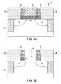
- FIG. 1is a pictorial representation of a prior art MOSFET including a gate stack comprising a high-k gate dielectric and a metal gate which is fabricated using a conventional gate replacement process as mentioned above.
- FIG. 1shows a prior art MOSFET structure that includes a semiconductor substrate 1000 that has source/drain diffusion regions 1004 located therein.
- the semiconductor substrate 1000also contains trench isolation regions 1006 that are filled with a trench dielectric material.
- a high-k gate dielectric 1008which is formed in the shape of a “U”, and a metal gate 1010 located within the U-shaped high-k gate dielectric 1008 .
- a dielectric spacer 1012is located on outer vertical sidewalls of the U-shaped high-k gate dielectric 1008 .
- the structure shown in FIG. 1also includes an interlevel dielectric material 1020 that has contact vias 1022 located therein which extend to the upper surface of the source/drain diffusion regions 1004 .
- the interlevel dielectric material 1020is laterally separated from the gate stack by the dielectric spacer 1012 .
- the presence of the metal gate 1010 on the vertical sidewalls of the U-shaped high-k gate dielectric 1008results in an undesired high contact-to-gate conductor parasitic capacitance.
- high-k gate dielectricAnother problem associated with a high-k gate dielectric is that the high-k gate dielectric at the gate corners (represented by the dotted circle shown in FIG. 1 ) may not be ideal due to variations in thickness and/or chemical component.
- a conventional gate reoxidation processcannot be used to strengthen the high-k gate dielectric at the gate corners because the high-k gate dielectric is sealed by the metal gate and the dielectric spacer.
- the non-ideal high-k gate dielectric at the gate cornersresults in high leakage and poor reliability.
- the present inventionprovides a high-k gate dielectric/metal gate MOSFET that has a reduced contact-to-gate conductor parasitic capacitance as compared to a high-k gate dielectric/metal gate MOSFET fabricated using a conventional gate replacement process.
- a reduction in the contact-to-gate conductor parasitic capacitance of about 10% or greateris achieved as compared with that of a prior art high-k gate dielectric/metal conductor MOSFET made using a conventional gate replacement process.
- the present inventionalso provides a high-k gate dielectric/metal gate MOSFET in which an improved high-k gate dielectric is present at the gate corners.
- the present inventionfurther provides, in some embodiments, a high-k gate dielectric/metal gate MOSFET that includes a low-k dielectric spacer located on vertical sidewalls of the metal gate.
- the low-k dielectric spacer employedhas a dielectric constant of less than 4, preferably less than 3.5. The presence of the low-k dielectric spacer aids in further lowering the contact-to-gate conductor parasitic capacitance.
- the present inventioneven further provides a high-k gate dielectric/metal gate MOSFET in which a channel region located beneath the high-k gate dielectric/metal gate stack has a length of about 2 ⁇ m or less.
- the present inventionprovides a semiconductor structure that comprises:
- MOSFETmetal oxide semiconductor field effect transistor
- a gate spacerlaterally abutting said metal-containing gate conductor and located upon an upper surface of both the gate dielectric and the high-k gate dielectric that is present at the gate corners.
- the inventive structurefurther comprises an interlevel dielectric material which contains conductively filled contact vias that extend to the surface of the semiconductor substrate which includes source/drain diffusion regions of the at least one MOSFET.
- the inventive structuremay further include a spacer liner present between the gate spacer and the interlevel dielectric material, the metal-containing gate conductor, and the upper surface of both the gate dielectric and the high-k gate dielectric that is present at the gate corners.
- the gate spaceris a low-k dielectric material (dielectric constant of less than 4).
- the gate spacerincludes a void present in the interior thereof which lowers the effective dielectric constant of the gate spacer.
- the high-k gate dielectric present at the gate cornersis strengthened by introducing oxygen and/or nitrogen into the material which is present at the gate corners.
- the present inventionalso provides a semiconductor structure that comprises:
- MOSFETmetal oxide semiconductor field effect transistor
- a gate spacerlaterally abutting said metal-containing gate conductor and located upon an upper surface of both the gate dielectric and the high-k gate dielectric that is present at the gate corners.
- the present inventionprovides a semiconductor structure that comprises:
- MOSFETmetal oxide semiconductor field effect transistor
- a low-k gate spacerthat includes voids in the interior thereof laterally abutting said metal-containing gate conductor and located upon an upper surface of both the gate dielectric and the high-k gate dielectric that is present at the gate corners.
- the present inventionalso provides a method of fabricating such a semiconductor structure.
- the method of the present inventionincludes:
- a structureincluding a sacrificial gate conductor and a gate dielectric located on a semiconductor substrate, said structure further including an interlevel dielectric located on said semiconductor substrate and separated from said sacrificial gate by a sacrificial spacer;
- a gate spacerin an area that previously included the sacrificial spacer and a portion of the U-shaped high-k gate dielectric.
- FIG. 1is a pictorial representation (through a cross sectional view) illustrating a prior art high-k gate dielectric/metal conductor MOSFET that was fabricated utilizing a conventional gate replacement process.
- FIGS. 2A , 2 B and 2 Care pictorial representations (through cross sectional views) illustrating high-k gate dielectric/metal-containing conductor MOSFETs in accordance with three embodiments of the present invention.
- FIGS. 3A-3Hare pictorial representations (through cross sectional views) illustrating the basic processing steps that can be used in fabricating the structures shown in FIGS. 2A-2C .
- the present inventionwhich provides a high-k gate dielectric/metal-containing MOSFET having at least reduced contact-to-gate conductor parasitic capacitance and a method of fabricating the same, will now be described in greater detail by referring to the following description and drawings that accompany the present application. It is noted that the drawings of the present application are provided for illustrative purposes only and, as such, the drawings are not drawn to scale.
- the present inventionis not limited to the same. Instead, a plurality of high-k gate dielectric/metal-containing conductor MOSFETs can be formed utilizing the method of the present invention.
- the plurality of high-k gate dielectric/metal-containing conductor MOSFETs that can be formedmay all have the same conductivity (i.e., nMOSFETs or pMOSFETs).
- the plurality of high-k gate dielectric/metal-containing conductor MOSFETscan include a first set of MOSFETs having a first conductivity (nMOSFETs or pMOSFETs) and a second set of MOSFETs having a second conductivity that differs from the first conductivity type MOSFET.
- the present inventionprovides a high-k gate dielectric/metal gate MOSFET that has a reduced contact-to-gate conductor parasitic capacitance as compared to a high-k gate dielectric/metal gate MOSFET fabricated using a conventional gate replacement process.
- FIGS. 2A-2Cshows various structural embodiments of the present invention.
- a first embodiment of the present inventionis shown.
- the structure shown in FIG. 2Aincludes at least one metal oxide semiconductor field effect transistor (MOSFET) 100 located on a surface of a semiconductor substrate 12 .
- the least one MOSFET 100includes a gate stack including, from bottom to top, a high-k gate dielectric 28 and a metal-containing gate conductor 30 .
- the metal-containing gate conductor 30has gate corners 31 located at a base segment of the metal-containing gate conductor.
- the base segment of the metal-containing gateis defined herein as the region of the gate conductor wherein the vertical sidewalls come into contact with the bottom wall of the gate conductor Moreover, the metal containing gate conductor 30 has vertical sidewalls 102 A and 10213 devoid of the high-k gate dielectric 28 except at the gate corners 31 ; the term “vertical sidewalls” is used to denote sidewalls that are perpendicular to a common bottom wall or they may have some tapering associated therewith. Also shown in FIG. 2A , is a gate dielectric 18 that laterally abuts the high-k gate dielectric 28 present at the gate corners 31 and a gate spacer 36 that laterally abuts the metal-containing gate conductor 30 . The gate spacer 36 is located upon an upper surface of both the gate dielectric 18 and the high-k gate dielectric 28 that is present at the gate corners 31 .
- the inventive structurefurther comprises an interlevel dielectric material 24 which contains conductively filled contact vias 40 that extend to the surface of the semiconductor substrate 12 which includes source/drain diffusion regions 14 of the at least one MOSFET 100 .
- a spacer liner 34is present between the gate spacer 36 and the interlevel dielectric material 24 , the metal-containing gate conductor 30 , and the upper surface of both the gate dielectric 18 and the high-k gate dielectric 28 that is present at the gate corners 31 .
- FIG. 2Ba second structural embodiment of the present invention is shown which comprises the same basic elements as that shown in FIG. 2A except that the high-k gate dielectric present at the gate corners has improved bonding as compared to the high-k gate dielectric that is located directly beneath the metal-containing gate conductor.
- reference numeral 28 ′denotes the high-k gate dielectric present at the gate corners 31 that has improved bonding
- reference numeral 28denotes the high-k gate dielectric directly beneath the metal-containing gate conductor 30 .
- FIG. 2Cillustrates a third structural embodiment of the present invention. Specifically, the structure shown in FIG. 2C comprises the same elements in FIG. 2B except that the gate spacer 36 includes a void 38 in the interior thereof. The presence of the void 38 lowers the effect dielectric constant of the gate spacer 36 .
- FIGS. 3A-3Hillustrate the basic processing steps that can be used in fabricating the inventive structures shown in FIGS. 2A-2C .
- the processing steps of the present inventioninclude first forming a conventional MOSFET with a dummy (i.e., sacrificial) gate, a gate dielectric, a sacrificial spacer and an interlevel dielectric.
- the sacrificial gate and the gate dielectric not protected by the sacrificial spacerare then removed to form an opening that exposes a surface of a semiconductor substrate.
- a U-shaped high-k gate dielectric and then a metal-containing gate conductorare formed inside the opening.
- the sacrificial spaceris then removed to expose a portion of the high-k gate dielectric that laterally abuts sidewalls of the metal-containing gate conductor.
- the exposed portion of the high-k gate dielectric that laterally abuts the sidewalls of the metal-containing gate conductoris then removed from the gate sidewalls and thereafter a spacer is formed.
- FIG. 3Aillustrates an initial semiconductor structure 10 that can be employed in the present invention.
- the initial semiconductor structure 10includes a semiconductor substrate 12 that has been processed to include at least one isolation region 16 and source/drain regions 14 .
- a silicide layer(not shown) may be present at the surface of the source/drain regions to lower the resistance.
- the semiconductor substrate 12further includes a gate dielectric 18 located on a surface of substrate 12 .
- the gate dielectric 18has a central portion that has a sacrificial gate 20 located thereon and outer edge portions that abut the central portion that each has a sacrificial spacer 22 located thereon.
- the vertical dotted linesare provided in FIG. 3A to shows the mythical boundaries between the central portion of the gate dielectric and the outer portions of the gate dielectric.
- the structure shown in FIG. 3Aalso includes an interlevel dielectric material 24 located on portions of the semiconductor substrate 12 not including the gate dielectric 18 , sacrificial gate 20 and sacrificial spacer 22 .
- the interlevel dielectric 24has an upper surface that is coplanar to an upper surface of the sacrificial gate 20 .
- the semiconductor substrate 12 shown in FIG. 3Aincludes any material that exhibits semiconductor properties. Examples of materials that exhibit semiconductor properties include, but are not limited to Si, SiGe, SiC, SiGeC, Ge, Ga, GaAs, InAs, InP and all other III/V or II/VI compound semiconductors.
- the semiconductor substrate 12may also comprise an organic semiconductor or a layered semiconductor such as, for example, Si/SiGe, a silicon-on-insulator or a SiGe-on-insulator.
- the semiconductor substrate 12comprises a Si-containing semiconductor material, i.e., a semiconductor material that includes silicon.
- the semiconductor substrate 12 employed in the present inventionmay also comprise a hybrid oriented (HOT) semiconductor substrate in which the HOT substrate has surface regions of different crystallographic orientation.
- HAThybrid oriented
- the semiconductor substrate 12may be doped, undoped or contain doped regions and undoped regions therein.
- the semiconductor substrate 12may be strained, unstrained, contain regions of strain and unstrain therein, or contain regions of tensile strain and compressive strain.
- Each isolation region 16 shown in FIG. 3Amay include a trench dielectric material such as an oxide and, optionally, a liner such as silicon nitride or silicon oxynitride may be present on the sidewalls of the trench.
- the trench isolation region 16is formed in the semiconductor substrate 12 prior to forming the other elements shown in FIG. 3A utilizing a conventional trench isolation process that includes first etching at least one trench in the semiconductor substrate 12 , optionally filling the at least one trench with a trench liner and thereafter filling the trench with a trench dielectric material.
- a conventional planarization processsuch as, for example, chemical mechanical polishing and/or grinding, is used to provide a planar structure.
- a densification processcan be performed after filling the trench with the trench dielectric material.
- trench isolation regionsis typically performed in the presence of a pad layer (not shown) that is removed from the structure after forming the at least one trench isolation region 16 in the semiconductor substrate 12 .
- the pad layermay comprise silicon nitride and optionally an underlying silicon oxide. Any conventional stripping process that selectively removes the pad layer can be used to remove the pad layer from the structure.
- each isolation region 16can be formed by other well known methods such as LOCOS (Local Oxidation Of Silicon).
- a blanket layer of gate dielectric 18is formed atop the entire surface of the semiconductor substrate 12 including atop the trench isolation regions 16 .
- the blanket layer of gate dielectric 18can be formed by a conventional deposition process including, for example, chemical vapor deposition (CVD), low pressure chemical vapor deposition (LPCVD), plasma enhanced chemical vapor deposition (PECVD), evaporation, chemical solution deposition, and atomic layer deposition (ALD).
- CVDchemical vapor deposition
- LPCVDlow pressure chemical vapor deposition
- PECVDplasma enhanced chemical vapor deposition
- ALDatomic layer deposition
- the blanket layer of gate dielectric 18has a thickness that is thicker that that of the high-k gate dielectric to be subsequently formed. Typically, the thickness of the gate dielectric 18 is from about 2 to about 20 nm, with a thickness from about 3 to about 10 nm being even more typical.
- the gate dielectric 18is typically an oxide of a semiconductor material, with an oxide of silicon being more typical.
- a blanket layer of sacrificial gate material(e.g., polysilicon or silicon germanium) is formed utilizing a conventional deposition process including, for example, CVD, LPCVD, PECVD, evaporation, chemical solution deposition and physical vapor deposition (PVD).
- the blanket layer of sacrificial gate material(which forms the sacrificial gate 20 ) has a thickness from about 20 to about 200 nm after deposition, with a thickness from about 50 to about 100 nm being even more typical.
- a patterning process that includes lithography and etchingis then used to pattern the blanket layer of sacrificial gate material into the sacrificial gate 20 shown in FIG. 3A .
- the lithographic stepincludes applying a photoresist to the surface of the blanket layer of sacrificial gate material, exposing the photoresist to a desired pattern of radiation and then developing the exposed resist.
- the etching stepincludes dry etching or wet etching. Preferably, a dry etching process such as reactive ion etching, ion beam etching and plasma etching is employed. The etching process stops on a surface of the gate dielectric 18 . After etching, the exposed and developed photoresist is removed from the structure utilizing a conventional resist stripping process such as, for example, ashing.
- each source/drain region 14may further comprise a source/drain extension region which is partially overlapped with the sacrificial gate 20 .
- Forming source/drain and source/drain extensionmay include utilizing conventional ion implantation process, spacer formation, and dopant activation anneal that are well known in the art.
- Sacrificial spacer 22is then formed on vertical sidewalls of the sacrificial gate 20 and atop a surface of the blanket layer of gate dielectric 18 by deposition and etching.
- the sacrificial spacer 22is comprised of a nitride-containing material such as silicon nitride or silicon oxynitride.
- the sacrificial spacer 22can be formed before or after the formation of the source and drain regions. If source/drain extension is formed, the sacrificial spacer 22 can be formed before or after the formation of the source/drain extension.
- the blanket layer of gate dielectric 18is etched utilizing the sacrificial spacer 22 and the sacrificial gate 20 as an etching mask.
- a blanket layer of the interlevel dielectric material 24is formed covering all exposed surfaces of the structure.
- the interlevel dielectric material 24is formed utilizing any conventional deposition process including, for example, chemical vapor deposition (CVD), low pressure chemical vapor deposition (LPCVD), plasma enhanced chemical vapor deposition (PECVD), sub-atmospheric chemical vapor deposition (SACVD), evaporation, chemical solution deposition, and spin-on-coating.
- the interlevel dielectric material 24includes any conventional dielectric material such as, for example, silicon dioxide, a silicate glass, a silsesquioxane, an organosilicate that includes atoms of Si, C, O and H, and a thermosetting polyarylene ether.
- polyaryleneis used to denote aryl moieties that are linked together by bonds, fused rings, or inert linking groups such as, for example, oxygen, sulfur, sulfone, sulfoxide, carbonyl and the like.
- a planarization processsuch as, for example, chemical mechanical polishing and/or grinding is then used to form a coplanar structure such as is shown in FIG. 3A .
- the initial structure shown in FIG. 3 Ais formed by first processing the substrate 12 to include the isolation regions 16 .
- the interlevel dielectric material 24is formed and lithography and etching are used to define at least one opening in the dielectric material that exposes a surface of the semiconductor substrate 12 .
- the source/drain regions 14can be formed at this point and thereafter the gate dielectric 18 is formed into the bottom of the opening.
- the sacrificial spacer 22is formed on the exposed sidewalls of the patterned interlevel dielectric material 24 and then the sacrificial gate 20 is formed.
- a planarization processis then typically used to provide the coplanar structure shown in FIG. 3A .
- This embodiment of the present inventionis typically employed to form a device channel whose length is about 2 ⁇ m or less.
- the sacrificial gate 20 and the sacrificial gate dielectric 18 that is located directly beneath the sacrificial gate 20is removed from the structure.
- the removal of the sacrificial gate 20 and the gate dielectric 18 beneath the sacrificial gate 20provides an opening 26 which exposes a surface of the semiconductor substrate 12 .
- the resultant structure that is formed after this step of the present invention has been performedis shown, for example, in FIG. 3B .
- various suitable processescan be used to remove those materials.
- a wet etching process with an etchant containing ammonia-based chemistry or a dry etching process such as a plasma etch with an etchant containing sulfuric fluoridecan be used to remove the sacrificial gate 20 comprising polysilicon.
- a wet etching process with an etchant of hydrofluoride acidcan be used to remove the gate dielectric 18 comprising silicon oxide.
- a U-shaped high-k gate dielectric 28is formed within the opening 26 and thereafter a metal-containing conductor 30 is formed on the exposed surfaces of the U-shaped high-k gate dielectric 28 providing the structure shown, for example, in FIG. 3C .
- the U-shaped high-k gate dielectric 28comprises any dielectric material whose dielectric constant is greater than 4.0, typically greater than 7.0. Examples of such high-k gate dielectric materials include but are not limited to TiO 2 , Al 2 O 3 , ZrO 2 , HfO 2 , Ta 2 O 5 , La 2 O 3 , mixed metal oxides such a perovskite-type oxides, and combinations and multilayers thereof.
- Silicates and nitrides of the aforementioned metal oxidescan also be used as the high-k gate dielectric material.
- a first interfacial layer(not shown) can be formed at the interface between the U-shaped high-k gate dielectric 28 and the substrate 12 to improve device characteristics such as reducing interface traps.
- the first interfacial layerif present, may comprise silicon oxide, silicon nitride, or oxynitride and can be formed by thermal oxidation, chemical oxidation, thermal nitridation, and chemical nitridation.
- a second interfacial layer(not shown) can be deposited at the top or within the U-shape high-k dielectric 28 before forming the metal-containing gate conductor 30 .
- the second interfacial layerhelps optimize device characteristics by adjusting the work function, and/or stabilizing the flatband voltage and threshold voltage.
- the second interfacial layerif present, may comprise a rare earth-containing layer comprising La 2 O 3 , LaN, or any other suitable materials.
- the U-shaped high-k gate dielectric 28can be formed by a conventional deposition process, including but not limited to, atomic layer deposition (ALD), chemical vapor deposition (CVD), low-pressure chemical vapor deposition (LPCVD), plasma enhanced chemical vapor deposition (PECVD), rapid thermal chemical vapor deposition (RTCVD), limited reaction processing CVD (LRPCVD), ultrahigh vacuum chemical vapor deposition (UHVCVD), metalorganic chemical vapor deposition (MOCVD), molecular beam epitaxy (MBE), physical vapor deposition, ion beam deposition, electron beam deposition, and laser assisted deposition.
- ALDatomic layer deposition
- CVDchemical vapor deposition
- LPCVDlow-pressure chemical vapor deposition
- PECVDplasma enhanced chemical vapor deposition
- RTCVDrapid thermal chemical vapor deposition
- LPCVDlimited reaction processing CVD
- UHVCVDultrahigh vacuum chemical vapor deposition
- MOCVDmetalorganic chemical vapor deposition
- the U-shaped high-k gate dielectric 28has a thickness that is less than that of the remaining outer portions of the gate dielectric 18 .
- the U-shaped high-k gate dielectric 28has a thickness from about 1 to about 20 nm, with a thickness from about 2 to about 10 nm being even more typical.
- the metal-containing gate conductor 30is formed utilizing a conventional deposition process such as, for example, atomic layer deposition (ALD), chemical vapor deposition (CVD), metalorganic chemical vapor deposition (MOCVD), molecular beam epitaxy (MBE), physical vapor deposition, sputtering, plating, evaporation, ion beam deposition, electron beam deposition, laser assisted deposition, and chemical solution deposition.
- ALDatomic layer deposition
- CVDchemical vapor deposition
- MOCVDmetalorganic chemical vapor deposition
- MBEmolecular beam epitaxy
- the metal-containing gate conductor 30includes a conductive metal such as, but not limited to Al, W, Cu, Pt, Ag, Au, Ru, Ir, Rh and Re, alloys of a conductive metal, e.g., Al—Cu, silicides of a conductive metal, e.g., W silicide, and Pt silicide, nitrides of a conductive metal, e.g., AIN, and combinations and multilayers thereof.
- a conventional planarization processsuch as chemical mechanical polishing (CMP) can be used to remove any metal-containing gate conductor 30 that is deposited at the top of the interlevel dielectric 24 and the sacrificial spacer 22 .
- a conventional etch processsuch as a wet etch or dry etch can be used to remove any U-shaped high-k gate dielectric 28 that is deposited at the top of the interlevel dielectric 24 and the sacrificial spacer 22 .
- the sacrificial spacer 22is removed from the structure exposing the remaining outer portions of the gate dielectric 18 , outer sidewalls of the U-shaped high-k gate dielectric 28 , and sidewalls of the interlevel dielectric material 24 .
- the sacrificial spacer 22is removed utilizing an etching process that selectively removes the material of the sacrificial spacer 22 as compared with the interlevel dielectric material 24 and the remaining gate dielectric 18 .
- etching processincludes a wet etch process with an etch etchant containing phosphoric acid or a mix of hydrofluoric and ethylene glycol (HF/EG) to remove the sacrificial spacer 22 which is formed of silicon nitride.
- etch etchantcontaining phosphoric acid or a mix of hydrofluoric and ethylene glycol (HF/EG)
- HF/EGhydrofluoric and ethylene glycol
- the sacrificial spacer 22when it comprises silicon nitride, can be removed by a dry etch process such as a chemical downstream etch (CDE).
- CDEchemical downstream etch
- FIG. 3Eshows the structure that is formed after removing the U-shaped high-k gate dielectric 28 from substantially all of the vertical sidewalls of the metal-containing gate conductor 30 .
- the presence of the thicker gate dielectric 18ensures that a substantially complete removal of the high-k gate material from the metal-containing gate sidewalls is obtained without undercutting the high-k gate dielectric material that is located beneath the metal-containing gate conductor 30 . Removing substantially all of the high-k gate dielectric material from the vertical sidewalls of the metal-containing gate conductor 30 reduces the contact-to-gate conductor capacitance.
- the U-shaped high-k gate dielectric 28however remains on the vertical sidewalls of the metal-containing gate conductor 30 covering the gate corners at the base segment of the metal-containing gate conductor 30 .
- the gate cornersare labeled by reference numeral 31 in FIG. 3E .
- the high-k gate material that remains at the gate corners 31has a height that is less than the height of the remaining gate dielectric 18 .
- the removal of the U-shaped high-k gate dielectric 28 from substantially all of the vertical sidewalls of the metal-containing gate conductor 30is performed utilizing an etching process that selectively removes the high gate dielectric material relative to that of the other materials that are exposed to the etching process.
- An example of such an etching processincludes a boron-halogen plasma which comprises a boron-halogen compound (e.g., BCl 3 ) and nitrogen.
- the high-k gate dielectric 28can be removed from the vertical sidewalls of the metal-containing gate conductor 30 simultaneously when removing the sacrificial spacer 22 .
- a portion of the remaining U-shaped high-k gate dielectric 28 that is not protected by the metal-containing gate conductor 30 which is located abutting the gate corners 31may be strengthen to reduce the leakage and reliability concerns that may exist at the gate corners 31 .
- increased leakage current and decreased reliability at the gate cornersmay exist due to stress and/or film deposition.
- the strengthened region of the remaining U-shaped high-k gate dielectric 28is labeled as 28 ′ in FIG. 3F .
- the strengtheningis achieved in the present invention by utilizing a low energy (on the order of about 20 KeV or less) oxygen ion and/or nitrogen ion implantation process.
- the dose of oxygen and/or nitrogen ions usedis typically within a range from about 1E12 to about 1E15 atoms/cm 2 , within a dose range from about 1E13 to about 1E14 atoms/cm 2 being more typical.
- a low temperature oxidation, nitridation or oxynitridation process(temperature on the order of about 950° C. or less) can be used to cause the above mentioned strengthen of the high-k gate material that is present at the gate corners 31 .
- the net effect of performing one of the above-mentioned techniquesis to improve the chemical bonding in the high-k gate dielectric material
- the high-k gate dielectric 28 located directly beneath the gate conductorhas a height h 3 that is less than the height h 2 of the remaining high-k gate dielectric at the gate corners and that the height h 2 of the remaining high-k gate dielectric at the gate corners is substantially the same or less than the height h 1 of the remaining gate dielectric 18 .
- the gate dielectrichas a first height
- the high-k gate dielectric that is present at the gate cornershas a second height
- the high-k gate dielectric located directly beneath said metal-containing gate conductorhas a third height, wherein said first height is substantially the same, or greater than, the second height, and said second height is greater than the third height.
- the remaining drawingsshow the presence of the strengthened high-k gate dielectric regions 28 ′ at the gate corners 31 . Although this is illustrated in the remaining drawings, the processing that follows can be used when the optional strengthening step has been omitted.
- FIG. 3Gshows the resultant structure that is formed after forming optional spacer liner 34 and gate spacer 36 within the space that was created when the sacrificial spacer 22 was removed and after substantially all of the high-k gate material located on the vertical sidewalls of the metal-containing gate conductor 20 was removed.
- the optional spacer liner 34comprises a first dielectric material which is different from the second dielectric material used in forming the gate spacer 36 .
- the spacer liner 34is comprised of silicon nitride and the gate spacer 36 is comprised of silicon dioxide.
- the gate spacer 36is a low-k (dielectric constant of less than 4.0) dielectric material such as, for example, an organosilicate that includes atoms of at least Si, C, O and H, and the spacer liner 34 comprises silicon oxide.
- the optional spacer liner 34has a thickness after deposition that is from about 1 to about 10 nm, with about 2 to 5 nm being more typical.
- the optional spacer liner 34can be formed by a deposition process such as, for example, atomic layer deposition (ALD), chemical vapor deposition (CVD), low-pressure chemical vapor deposition (LPCVD), plasma enhanced chemical vapor deposition (PECVD), sub-atmospheric chemical vapor deposition (SACVD), rapid thermal chemical vapor deposition (RTCVD), high temperature oxide deposition (HTO), low temperature oxide deposition (LTO), limited reaction processing CVD (LRPCVD), spin-on-coating, chemical solution deposition, or any other suitable process.
- ALDatomic layer deposition
- CVDchemical vapor deposition
- LPCVDlow-pressure chemical vapor deposition
- PECVDplasma enhanced chemical vapor deposition
- SACVDsub-atmospheric chemical vapor deposition
- RTCVDrapid thermal chemical vapor de
- the gate spacer 36is formed by any suitable deposition process such as CVD and spin-on-coating. It is pointed out herein that a bottom surface of the gate spacer 36 is located atop, or directly on, both the remaining gate dielectric 18 and the high-k gate dielectric that is present at the gate corners 31 . In a conventional prior art structure, the gate spacer is located directly on a surface of the semiconductor substrate.
- a void 38(see FIG. 2C ) can be present in an interior portion of the gate spacer 36 .
- the presence of the voidhas the effect of further reducing the effective dielectric constant of the gate spacer 36 that is employed in the present invention.
- FIG. 3Hillustrates the structure after conductively filled contact vias 40 are formed in the interlevel dielectric material 24 which extend to the surface of the semiconductor substrate 12 that includes the source/drain diffusion regions 14 .
- the conductively filled contact vias 40are formed by lithography, etching and filling the contact via thus formed with a conductive material.
- a diffusion barriersuch as TiN or TaN can be formed on the exposed sidewalls of the contact via prior to filling the via with the conductive material.
- the conductive material used in filling the contact openingsincludes any conductive material including one of the conductive materials used in forming the metal-containing gate conductor 30 .
- the conductively filled contacts vias 40can be formed into the interlevel dielectric material 24 prior to removing the high-k gate dielectric 28 and the sacrificial spacer 22 from the vertical sidewall of the metal-containing gate conductor 30 .
Landscapes
- Insulated Gate Type Field-Effect Transistor (AREA)
Abstract
Description
- This application is a divisional of U.S. patent application Ser. No. 11/769,150, filed Jun. 27, 2007 the entire content and disclosure of which is incorporated herein by reference.
- The present invention relates to a semiconductor structure and a method of fabricating the same. More particularly, the present invention relates to a metal oxide semiconductor field effect transistor (MOSFET) including a high dielectric constant (k) gate dielectric and a metal-containing gate conductor that has reduced parasitic capacitance. The present invention also provides a method of fabricating such a MOSFET.
- In the semiconductor industry, a gate stack including a high-k gate dielectric (a gate dielectric having a dielectric constant of greater than 4.0, typically greater than 7.0) and a metal gate is one of the most promising options for continuing complementary metal oxide semiconductor (CMOS) scaling.
- One of the process schemes for fabricating a high-k/metal gate MOSFET is a replacement gate method. In a replacement gate process, a MOSFET can be fabricated using a sacrificial gate electrode. In such a process, the sacrificial gate electrode is formed first and thereafter the sacrificial gate electrode is replaced by a gate stack including a high-k gate dielectric and a metal gate. Since the gate stack including the high-k gate dielectric and the metal gate is formed after high temperature processing steps such as a source/drain activation anneal, the replacement gate process has the advantage of minimal damage on the high-k gate dielectric and the metal gate. Moreover, a wide range of metals can be selected for the gate conductor.
- One severe drawback of a conventional gate replacement process results in the high-k gate dielectric being present not only beneath the metal gate, but also on vertical sidewalls of the metal gate.
FIG. 1 is a pictorial representation of a prior art MOSFET including a gate stack comprising a high-k gate dielectric and a metal gate which is fabricated using a conventional gate replacement process as mentioned above. In particular,FIG. 1 shows a prior art MOSFET structure that includes asemiconductor substrate 1000 that has source/drain diffusion regions 1004 located therein. Thesemiconductor substrate 1000 also containstrench isolation regions 1006 that are filled with a trench dielectric material. Atop thesemiconductor substrate 1000, there is shown a high-k gate dielectric1008, which is formed in the shape of a “U”, and ametal gate 1010 located within the U-shaped high-k gate dielectric1008. Adielectric spacer 1012 is located on outer vertical sidewalls of the U-shaped high-k gate dielectric1008. The structure shown inFIG. 1 also includes an interleveldielectric material 1020 that hascontact vias 1022 located therein which extend to the upper surface of the source/drain diffusion regions 1004. The interleveldielectric material 1020 is laterally separated from the gate stack by thedielectric spacer 1012.- The presence of the
metal gate 1010 on the vertical sidewalls of the U-shaped high-k gate dielectric1008 results in an undesired high contact-to-gate conductor parasitic capacitance. - Another problem associated with a high-k gate dielectric is that the high-k gate dielectric at the gate corners (represented by the dotted circle shown in
FIG. 1 ) may not be ideal due to variations in thickness and/or chemical component. A conventional gate reoxidation process cannot be used to strengthen the high-k gate dielectric at the gate corners because the high-k gate dielectric is sealed by the metal gate and the dielectric spacer. The non-ideal high-k gate dielectric at the gate corners results in high leakage and poor reliability. - In view of the above, there is a need for a new and improved high-k/metal gate MOSFET with reduced contact-to-gate conductor parasitic capacitance and, optionally, an improved high-k gate dielectric at the gate corners.
- The present invention provides a high-k gate dielectric/metal gate MOSFET that has a reduced contact-to-gate conductor parasitic capacitance as compared to a high-k gate dielectric/metal gate MOSFET fabricated using a conventional gate replacement process. In the present invention, a reduction in the contact-to-gate conductor parasitic capacitance of about 10% or greater is achieved as compared with that of a prior art high-k gate dielectric/metal conductor MOSFET made using a conventional gate replacement process.
- The present invention also provides a high-k gate dielectric/metal gate MOSFET in which an improved high-k gate dielectric is present at the gate corners.
- The present invention further provides, in some embodiments, a high-k gate dielectric/metal gate MOSFET that includes a low-k dielectric spacer located on vertical sidewalls of the metal gate. The low-k dielectric spacer employed has a dielectric constant of less than 4, preferably less than 3.5. The presence of the low-k dielectric spacer aids in further lowering the contact-to-gate conductor parasitic capacitance.
- The present invention even further provides a high-k gate dielectric/metal gate MOSFET in which a channel region located beneath the high-k gate dielectric/metal gate stack has a length of about 2 μm or less.
- In general terms, the present invention provides a semiconductor structure that comprises:
- at least one metal oxide semiconductor field effect transistor (MOSFET) located on a surface of a semiconductor substrate, said at least one MOSFET comprising a gate stack including, from bottom to top, a high-k gate dielectric and a metal-containing gate conductor, said metal-containing gate conductor having gate corners located at a base segment of the metal-containing gate conductor, wherein said metal-containing gate conductor has vertical sidewalls devoid of said high-k gate dielectric except at said gate corners;
- a gate dielectric laterally abutting said high-k gate dielectric present at said gate corners; and
- a gate spacer laterally abutting said metal-containing gate conductor and located upon an upper surface of both the gate dielectric and the high-k gate dielectric that is present at the gate corners.
- The inventive structure further comprises an interlevel dielectric material which contains conductively filled contact vias that extend to the surface of the semiconductor substrate which includes source/drain diffusion regions of the at least one MOSFET.
- In some embodiments of the present invention, the inventive structure may further include a spacer liner present between the gate spacer and the interlevel dielectric material, the metal-containing gate conductor, and the upper surface of both the gate dielectric and the high-k gate dielectric that is present at the gate corners.
- In yet another embodiment of the present invention, the gate spacer is a low-k dielectric material (dielectric constant of less than 4). In a further embodiment, the gate spacer includes a void present in the interior thereof which lowers the effective dielectric constant of the gate spacer.
- In an even further embodiment of the present invention, the high-k gate dielectric present at the gate corners is strengthened by introducing oxygen and/or nitrogen into the material which is present at the gate corners.
- In addition to the general semiconductor structure mentioned above, the present invention also provides a semiconductor structure that comprises:
- at least one metal oxide semiconductor field effect transistor (MOSFET) located on a surface of a semiconductor substrate, said at least one MOSFET comprising a gate stack including, from bottom to top, a high-k gate dielectric and a metal-containing gate conductor, said metal-containing gate conductor having gate corners located at a base segment of the metal-containing gate conductor, wherein said metal-containing gate conductor has vertical sidewalls devoid of said high-k gate dielectric except at said gate corners, said high-k gate dielectric at said gate corners has increased bonding as compared to said high-k gate dielectric that is located directly beneath said metal-containing gate conductor;
- a gate dielectric laterally abutting said high-k gate dielectric present at said gate corners; and
- a gate spacer laterally abutting said metal-containing gate conductor and located upon an upper surface of both the gate dielectric and the high-k gate dielectric that is present at the gate corners.
- In another embodiment, the present invention provides a semiconductor structure that comprises:
- at least one metal oxide semiconductor field effect transistor (MOSFET) located on a surface of a semiconductor substrate, said at least one MOSFET comprising a gate stack including, from bottom to top, a high-k gate dielectric and a metal-containing gate conductor, said metal-containing gate conductor having gate corners located at a base segment of the metal-containing gate conductor, wherein said metal containing gate conductor has vertical sidewalls devoid of said high-k gate dielectric except at said gate corners;
- a gate dielectric laterally abutting said high-k gate dielectric present at said gate corners; and
- a low-k gate spacer that includes voids in the interior thereof laterally abutting said metal-containing gate conductor and located upon an upper surface of both the gate dielectric and the high-k gate dielectric that is present at the gate corners.
- In addition to the semiconductor structure described above, the present invention also provides a method of fabricating such a semiconductor structure. In general terms, the method of the present invention includes:
- providing a structure including a sacrificial gate conductor and a gate dielectric located on a semiconductor substrate, said structure further including an interlevel dielectric located on said semiconductor substrate and separated from said sacrificial gate by a sacrificial spacer;
- removing the sacrificial gate and a portion of the gate dielectric that is not protected by the sacrificial spacer to form an opening that exposes a surface of the semiconductor substrate;
- forming a U-shaped high-k gate dielectric and a metal-containing gate conductor inside the opening;
- removing the sacrificial spacer to expose a portion of the U-shaped high-k gate dielectric that laterally abuts sidewalls of the metal-containing gate conductor;
- removing substantially all of the exposed portion of the high-k gate dielectric that laterally abuts the sidewalls of the metal-containing gate conductor from the gate sidewalls; and
- forming a gate spacer in an area that previously included the sacrificial spacer and a portion of the U-shaped high-k gate dielectric.
FIG. 1 is a pictorial representation (through a cross sectional view) illustrating a prior art high-k gate dielectric/metal conductor MOSFET that was fabricated utilizing a conventional gate replacement process.FIGS. 2A ,2B and2C are pictorial representations (through cross sectional views) illustrating high-k gate dielectric/metal-containing conductor MOSFETs in accordance with three embodiments of the present invention.FIGS. 3A-3H are pictorial representations (through cross sectional views) illustrating the basic processing steps that can be used in fabricating the structures shown inFIGS. 2A-2C .- The present invention which provides a high-k gate dielectric/metal-containing MOSFET having at least reduced contact-to-gate conductor parasitic capacitance and a method of fabricating the same, will now be described in greater detail by referring to the following description and drawings that accompany the present application. It is noted that the drawings of the present application are provided for illustrative purposes only and, as such, the drawings are not drawn to scale.
- In the following description, numerous specific details are set forth, such as particular structures, components, materials, dimensions, processing steps and techniques, in order to provide a thorough understanding of the present invention. However, it will be appreciated by one of ordinary skill in the art that the invention may be practiced without these specific details. In other instances, well-known structures or processing steps have not been described in detail in order to avoid obscuring the invention.
- It will be understood that when an element as a layer, region or substrate is referred to as being “on” or “over” another element, it can be directly on the other element or intervening elements may also be present. In contrast, when an element is referred to as being “directly on” or “directly over” another element, there are no intervening elements present. It will also be understood that when an element is referred to as being “beneath” or “under” another element, it can be directly beneath or under the other element, or intervening elements may be present. In contrast, when an element is referred to as being “directly beneath” or “directly under” another element, there are no intervening elements present.
- Also, it is observed that although the following description and drawings show the presence of a single high-k gate dielectric/metal-containing conductor MOSFET, the present invention is not limited to the same. Instead, a plurality of high-k gate dielectric/metal-containing conductor MOSFETs can be formed utilizing the method of the present invention. The plurality of high-k gate dielectric/metal-containing conductor MOSFETs that can be formed may all have the same conductivity (i.e., nMOSFETs or pMOSFETs). Alternatively, the plurality of high-k gate dielectric/metal-containing conductor MOSFETs can include a first set of MOSFETs having a first conductivity (nMOSFETs or pMOSFETs) and a second set of MOSFETs having a second conductivity that differs from the first conductivity type MOSFET.
- As stated above, the present invention provides a high-k gate dielectric/metal gate MOSFET that has a reduced contact-to-gate conductor parasitic capacitance as compared to a high-k gate dielectric/metal gate MOSFET fabricated using a conventional gate replacement process.
FIGS. 2A-2C shows various structural embodiments of the present invention. InFIG. 2A , a first embodiment of the present invention is shown. The structure shown inFIG. 2A includes at least one metal oxide semiconductor field effect transistor (MOSFET)100 located on a surface of asemiconductor substrate 12. The least oneMOSFET 100 includes a gate stack including, from bottom to top, a high-k gate dielectric 28 and a metal-containinggate conductor 30. The metal-containinggate conductor 30 hasgate corners 31 located at a base segment of the metal-containing gate conductor. The base segment of the metal-containing gate is defined herein as the region of the gate conductor wherein the vertical sidewalls come into contact with the bottom wall of the gate conductor Moreover, the metal containinggate conductor 30 hasvertical sidewalls 102A and10213 devoid of the high-k gate dielectric 28 except at thegate corners 31; the term “vertical sidewalls” is used to denote sidewalls that are perpendicular to a common bottom wall or they may have some tapering associated therewith. Also shown inFIG. 2A , is agate dielectric 18 that laterally abuts the high-k gate dielectric 28 present at thegate corners 31 and agate spacer 36 that laterally abuts the metal-containinggate conductor 30. Thegate spacer 36 is located upon an upper surface of both thegate dielectric 18 and the high-k gate dielectric 28 that is present at thegate corners 31.- The inventive structure further comprises an interlevel
dielectric material 24 which contains conductively filled contact vias40 that extend to the surface of thesemiconductor substrate 12 which includes source/drain diffusion regions 14 of the at least oneMOSFET 100. - In some embodiments of the present invention, a
spacer liner 34 is present between thegate spacer 36 and the interleveldielectric material 24, the metal-containinggate conductor 30, and the upper surface of both thegate dielectric 18 and the high-k gate dielectric 28 that is present at thegate corners 31. - With respect to
FIG. 2B , a second structural embodiment of the present invention is shown which comprises the same basic elements as that shown inFIG. 2A except that the high-k gate dielectric present at the gate corners has improved bonding as compared to the high-k gate dielectric that is located directly beneath the metal-containing gate conductor. InFIG. 2B ,reference numeral 28′ denotes the high-k gate dielectric present at thegate corners 31 that has improved bonding, whilereference numeral 28 denotes the high-k gate dielectric directly beneath the metal-containinggate conductor 30. FIG. 2C illustrates a third structural embodiment of the present invention. Specifically, the structure shown inFIG. 2C comprises the same elements inFIG. 2B except that thegate spacer 36 includes a void38 in the interior thereof. The presence of the void38 lowers the effect dielectric constant of thegate spacer 36.- Reference is now made to
FIGS. 3A-3H which illustrate the basic processing steps that can be used in fabricating the inventive structures shown inFIGS. 2A-2C . The processing steps of the present invention include first forming a conventional MOSFET with a dummy (i.e., sacrificial) gate, a gate dielectric, a sacrificial spacer and an interlevel dielectric. The sacrificial gate and the gate dielectric not protected by the sacrificial spacer are then removed to form an opening that exposes a surface of a semiconductor substrate. A U-shaped high-k gate dielectric and then a metal-containing gate conductor are formed inside the opening. The sacrificial spacer is then removed to expose a portion of the high-k gate dielectric that laterally abuts sidewalls of the metal-containing gate conductor. The exposed portion of the high-k gate dielectric that laterally abuts the sidewalls of the metal-containing gate conductor is then removed from the gate sidewalls and thereafter a spacer is formed. - Reference is first made to
FIG. 3A which illustrates aninitial semiconductor structure 10 that can be employed in the present invention. As is illustrated, theinitial semiconductor structure 10 includes asemiconductor substrate 12 that has been processed to include at least oneisolation region 16 and source/drain regions 14. A silicide layer (not shown) may be present at the surface of the source/drain regions to lower the resistance. Thesemiconductor substrate 12 further includes agate dielectric 18 located on a surface ofsubstrate 12. Thegate dielectric 18 has a central portion that has asacrificial gate 20 located thereon and outer edge portions that abut the central portion that each has asacrificial spacer 22 located thereon. The vertical dotted lines are provided inFIG. 3A to shows the mythical boundaries between the central portion of the gate dielectric and the outer portions of the gate dielectric. - The structure shown in
FIG. 3A also includes an interleveldielectric material 24 located on portions of thesemiconductor substrate 12 not including thegate dielectric 18,sacrificial gate 20 andsacrificial spacer 22. As is shown, theinterlevel dielectric 24 has an upper surface that is coplanar to an upper surface of thesacrificial gate 20. - The
semiconductor substrate 12 shown inFIG. 3A includes any material that exhibits semiconductor properties. Examples of materials that exhibit semiconductor properties include, but are not limited to Si, SiGe, SiC, SiGeC, Ge, Ga, GaAs, InAs, InP and all other III/V or II/VI compound semiconductors. Thesemiconductor substrate 12 may also comprise an organic semiconductor or a layered semiconductor such as, for example, Si/SiGe, a silicon-on-insulator or a SiGe-on-insulator. In some embodiments of the present invention, it is preferred that thesemiconductor substrate 12 comprises a Si-containing semiconductor material, i.e., a semiconductor material that includes silicon. In addition to the aforementioned types of semiconductor substrates, thesemiconductor substrate 12 employed in the present invention may also comprise a hybrid oriented (HOT) semiconductor substrate in which the HOT substrate has surface regions of different crystallographic orientation. - The
semiconductor substrate 12 may be doped, undoped or contain doped regions and undoped regions therein. Thesemiconductor substrate 12 may be strained, unstrained, contain regions of strain and unstrain therein, or contain regions of tensile strain and compressive strain. - Each
isolation region 16 shown inFIG. 3A may include a trench dielectric material such as an oxide and, optionally, a liner such as silicon nitride or silicon oxynitride may be present on the sidewalls of the trench. Thetrench isolation region 16 is formed in thesemiconductor substrate 12 prior to forming the other elements shown inFIG. 3A utilizing a conventional trench isolation process that includes first etching at least one trench in thesemiconductor substrate 12, optionally filling the at least one trench with a trench liner and thereafter filling the trench with a trench dielectric material. After trench fill, a conventional planarization process such as, for example, chemical mechanical polishing and/or grinding, is used to provide a planar structure. In some embodiments, a densification process can be performed after filling the trench with the trench dielectric material. - It is noted that the formation of trench isolation regions is typically performed in the presence of a pad layer (not shown) that is removed from the structure after forming the at least one
trench isolation region 16 in thesemiconductor substrate 12. The pad layer may comprise silicon nitride and optionally an underlying silicon oxide. Any conventional stripping process that selectively removes the pad layer can be used to remove the pad layer from the structure. - Alternatively, each
isolation region 16 can be formed by other well known methods such as LOCOS (Local Oxidation Of Silicon). - At this point of the present invention one of two different processing sequences can be used to fabricate the structure shown in
FIG. 3A . In a first processing sequence in which a conventional CMOS processing flow is used, a blanket layer ofgate dielectric 18 is formed atop the entire surface of thesemiconductor substrate 12 including atop thetrench isolation regions 16. The blanket layer of gate dielectric18 can be formed by a conventional deposition process including, for example, chemical vapor deposition (CVD), low pressure chemical vapor deposition (LPCVD), plasma enhanced chemical vapor deposition (PECVD), evaporation, chemical solution deposition, and atomic layer deposition (ALD). Alternatively, thermal oxidation, nitridation or oxynitridation can be used to form the blanket layer ofgate dielectric 18. The blanket layer ofgate dielectric 18 has a thickness that is thicker that that of the high-k gate dielectric to be subsequently formed. Typically, the thickness of thegate dielectric 18 is from about 2 to about 20 nm, with a thickness from about 3 to about 10 nm being even more typical. Thegate dielectric 18 is typically an oxide of a semiconductor material, with an oxide of silicon being more typical. - After forming the blanket layer of
gate dielectric 18, a blanket layer of sacrificial gate material (e.g., polysilicon or silicon germanium) is formed utilizing a conventional deposition process including, for example, CVD, LPCVD, PECVD, evaporation, chemical solution deposition and physical vapor deposition (PVD). The blanket layer of sacrificial gate material (which forms the sacrificial gate20) has a thickness from about 20 to about 200 nm after deposition, with a thickness from about 50 to about 100 nm being even more typical. - A patterning process that includes lithography and etching is then used to pattern the blanket layer of sacrificial gate material into the
sacrificial gate 20 shown inFIG. 3A . The lithographic step includes applying a photoresist to the surface of the blanket layer of sacrificial gate material, exposing the photoresist to a desired pattern of radiation and then developing the exposed resist. The etching step includes dry etching or wet etching. Preferably, a dry etching process such as reactive ion etching, ion beam etching and plasma etching is employed. The etching process stops on a surface of thegate dielectric 18. After etching, the exposed and developed photoresist is removed from the structure utilizing a conventional resist stripping process such as, for example, ashing. - At this point, the source/
drain regions 14 are formed into thesemiconductor substrate 12. Each source/drain region 14 may further comprise a source/drain extension region which is partially overlapped with thesacrificial gate 20. Forming source/drain and source/drain extension may include utilizing conventional ion implantation process, spacer formation, and dopant activation anneal that are well known in the art. Sacrificial spacer 22 is then formed on vertical sidewalls of thesacrificial gate 20 and atop a surface of the blanket layer ofgate dielectric 18 by deposition and etching. Thesacrificial spacer 22 is comprised of a nitride-containing material such as silicon nitride or silicon oxynitride. Thesacrificial spacer 22 can be formed before or after the formation of the source and drain regions. If source/drain extension is formed, thesacrificial spacer 22 can be formed before or after the formation of the source/drain extension.- Next, the blanket layer of
gate dielectric 18 is etched utilizing thesacrificial spacer 22 and thesacrificial gate 20 as an etching mask. - A blanket layer of the interlevel
dielectric material 24 is formed covering all exposed surfaces of the structure. The interleveldielectric material 24 is formed utilizing any conventional deposition process including, for example, chemical vapor deposition (CVD), low pressure chemical vapor deposition (LPCVD), plasma enhanced chemical vapor deposition (PECVD), sub-atmospheric chemical vapor deposition (SACVD), evaporation, chemical solution deposition, and spin-on-coating. The interleveldielectric material 24 includes any conventional dielectric material such as, for example, silicon dioxide, a silicate glass, a silsesquioxane, an organosilicate that includes atoms of Si, C, O and H, and a thermosetting polyarylene ether. The term “polyarylene” is used to denote aryl moieties that are linked together by bonds, fused rings, or inert linking groups such as, for example, oxygen, sulfur, sulfone, sulfoxide, carbonyl and the like. - A planarization process such as, for example, chemical mechanical polishing and/or grinding is then used to form a coplanar structure such as is shown in
FIG. 3A . - In another processing sequence, the initial structure shown in
FIG. 3 A is formed by first processing thesubstrate 12 to include theisolation regions 16. Next, the interleveldielectric material 24 is formed and lithography and etching are used to define at least one opening in the dielectric material that exposes a surface of thesemiconductor substrate 12. The source/drain regions 14 can be formed at this point and thereafter thegate dielectric 18 is formed into the bottom of the opening. Next, thesacrificial spacer 22 is formed on the exposed sidewalls of the patterned interleveldielectric material 24 and then thesacrificial gate 20 is formed. A planarization process is then typically used to provide the coplanar structure shown inFIG. 3A . This embodiment of the present invention is typically employed to form a device channel whose length is about 2 μm or less. - After providing the
initial structure 10 shown inFIG. 3A , thesacrificial gate 20 and the sacrificial gate dielectric18 that is located directly beneath thesacrificial gate 20 is removed from the structure. The removal of thesacrificial gate 20 and thegate dielectric 18 beneath thesacrificial gate 20 provides anopening 26 which exposes a surface of thesemiconductor substrate 12. The resultant structure that is formed after this step of the present invention has been performed is shown, for example, inFIG. 3B . Depending on the materials of thesacrificial gate 20 and thegate dielectric 18, various suitable processes can be used to remove those materials. For example, a wet etching process with an etchant containing ammonia-based chemistry or a dry etching process such as a plasma etch with an etchant containing sulfuric fluoride can be used to remove thesacrificial gate 20 comprising polysilicon. A wet etching process with an etchant of hydrofluoride acid can be used to remove thegate dielectric 18 comprising silicon oxide. - Next, a U-shaped high-
k gate dielectric 28 is formed within theopening 26 and thereafter a metal-containingconductor 30 is formed on the exposed surfaces of the U-shaped high-k gate dielectric 28 providing the structure shown, for example, inFIG. 3C . The U-shaped high-k gate dielectric 28 comprises any dielectric material whose dielectric constant is greater than 4.0, typically greater than 7.0. Examples of such high-k gate dielectric materials include but are not limited to TiO2, Al2O3, ZrO2, HfO2, Ta2O5, La2O3, mixed metal oxides such a perovskite-type oxides, and combinations and multilayers thereof. Silicates and nitrides of the aforementioned metal oxides can also be used as the high-k gate dielectric material. Optionally, a first interfacial layer (not shown) can be formed at the interface between the U-shaped high-k gate dielectric 28 and thesubstrate 12 to improve device characteristics such as reducing interface traps. The first interfacial layer, if present, may comprise silicon oxide, silicon nitride, or oxynitride and can be formed by thermal oxidation, chemical oxidation, thermal nitridation, and chemical nitridation. Furthermore, a second interfacial layer (not shown) can be deposited at the top or within the U-shape high-k dielectric 28 before forming the metal-containinggate conductor 30. The second interfacial layer, if present, helps optimize device characteristics by adjusting the work function, and/or stabilizing the flatband voltage and threshold voltage. The second interfacial layer, if present, may comprise a rare earth-containing layer comprising La2O3, LaN, or any other suitable materials. The U-shaped high-k gate dielectric 28 can be formed by a conventional deposition process, including but not limited to, atomic layer deposition (ALD), chemical vapor deposition (CVD), low-pressure chemical vapor deposition (LPCVD), plasma enhanced chemical vapor deposition (PECVD), rapid thermal chemical vapor deposition (RTCVD), limited reaction processing CVD (LRPCVD), ultrahigh vacuum chemical vapor deposition (UHVCVD), metalorganic chemical vapor deposition (MOCVD), molecular beam epitaxy (MBE), physical vapor deposition, ion beam deposition, electron beam deposition, and laser assisted deposition. - The U-shaped high-
k gate dielectric 28 has a thickness that is less than that of the remaining outer portions of thegate dielectric 18. Typically, the U-shaped high-k gate dielectric 28 has a thickness from about 1 to about 20 nm, with a thickness from about 2 to about 10 nm being even more typical. - The metal-containing
gate conductor 30 is formed utilizing a conventional deposition process such as, for example, atomic layer deposition (ALD), chemical vapor deposition (CVD), metalorganic chemical vapor deposition (MOCVD), molecular beam epitaxy (MBE), physical vapor deposition, sputtering, plating, evaporation, ion beam deposition, electron beam deposition, laser assisted deposition, and chemical solution deposition. The metal-containinggate conductor 30 includes a conductive metal such as, but not limited to Al, W, Cu, Pt, Ag, Au, Ru, Ir, Rh and Re, alloys of a conductive metal, e.g., Al—Cu, silicides of a conductive metal, e.g., W silicide, and Pt silicide, nitrides of a conductive metal, e.g., AIN, and combinations and multilayers thereof. A conventional planarization process such as chemical mechanical polishing (CMP) can be used to remove any metal-containinggate conductor 30 that is deposited at the top of theinterlevel dielectric 24 and thesacrificial spacer 22. A conventional etch process such as a wet etch or dry etch can be used to remove any U-shaped high-k gate dielectric 28 that is deposited at the top of theinterlevel dielectric 24 and thesacrificial spacer 22. - Next, and as shown in
FIG. 3D , thesacrificial spacer 22 is removed from the structure exposing the remaining outer portions of thegate dielectric 18, outer sidewalls of the U-shaped high-k gate dielectric 28, and sidewalls of the interleveldielectric material 24. Thesacrificial spacer 22 is removed utilizing an etching process that selectively removes the material of thesacrificial spacer 22 as compared with the interleveldielectric material 24 and the remaininggate dielectric 18. An example of such an etching process that can be used includes a wet etch process with an etch etchant containing phosphoric acid or a mix of hydrofluoric and ethylene glycol (HF/EG) to remove thesacrificial spacer 22 which is formed of silicon nitride. Alternatively, thesacrificial spacer 22, when it comprises silicon nitride, can be removed by a dry etch process such as a chemical downstream etch (CDE). FIG. 3E shows the structure that is formed after removing the U-shaped high-k gate dielectric28 from substantially all of the vertical sidewalls of the metal-containinggate conductor 30. The presence of thethicker gate dielectric 18 ensures that a substantially complete removal of the high-k gate material from the metal-containing gate sidewalls is obtained without undercutting the high-k gate dielectric material that is located beneath the metal-containinggate conductor 30. Removing substantially all of the high-k gate dielectric material from the vertical sidewalls of the metal-containinggate conductor 30 reduces the contact-to-gate conductor capacitance.- It is noted that some portion of the U-shaped high-
k gate dielectric 28 however remains on the vertical sidewalls of the metal-containinggate conductor 30 covering the gate corners at the base segment of the metal-containinggate conductor 30. The gate corners are labeled byreference numeral 31 inFIG. 3E . In the present invention, the high-k gate material that remains at thegate corners 31 has a height that is less than the height of the remaininggate dielectric 18. - The removal of the U-shaped high-k gate dielectric28 from substantially all of the vertical sidewalls of the metal-containing
gate conductor 30 is performed utilizing an etching process that selectively removes the high gate dielectric material relative to that of the other materials that are exposed to the etching process. An example of such an etching process includes a boron-halogen plasma which comprises a boron-halogen compound (e.g., BCl3) and nitrogen. Alternatively, the high-k gate dielectric 28 can be removed from the vertical sidewalls of the metal-containinggate conductor 30 simultaneously when removing thesacrificial spacer 22. - In some embodiments of the present invention, a portion of the remaining U-shaped high-
k gate dielectric 28 that is not protected by the metal-containinggate conductor 30 which is located abutting thegate corners 31 may be strengthen to reduce the leakage and reliability concerns that may exist at thegate corners 31. When using a high-k gate dielectric material, increased leakage current and decreased reliability at the gate corners may exist due to stress and/or film deposition. The strengthened region of the remaining U-shaped high-k gate dielectric 28 is labeled as28′ inFIG. 3F . - The strengthening is achieved in the present invention by utilizing a low energy (on the order of about 20 KeV or less) oxygen ion and/or nitrogen ion implantation process. The dose of oxygen and/or nitrogen ions used is typically within a range from about 1E12 to about 1E15 atoms/cm2, within a dose range from about 1E13 to about 1E14 atoms/cm2being more typical. Alternatively, a low temperature oxidation, nitridation or oxynitridation process (temperature on the order of about 950° C. or less) can be used to cause the above mentioned strengthen of the high-k gate material that is present at the
gate corners 31. The net effect of performing one of the above-mentioned techniques is to improve the chemical bonding in the high-k gate dielectric material - It is mentioned here that in the present invention the high-
k gate dielectric 28 located directly beneath the gate conductor has a height h3that is less than the height h2of the remaining high-k gate dielectric at the gate corners and that the height h2of the remaining high-k gate dielectric at the gate corners is substantially the same or less than the height h1of the remaininggate dielectric 18. In other terms, the gate dielectric has a first height, the high-k gate dielectric that is present at the gate corners has a second height, and the high-k gate dielectric located directly beneath said metal-containing gate conductor has a third height, wherein said first height is substantially the same, or greater than, the second height, and said second height is greater than the third height. - The remaining drawings show the presence of the strengthened high-k gate
dielectric regions 28′ at thegate corners 31. Although this is illustrated in the remaining drawings, the processing that follows can be used when the optional strengthening step has been omitted. FIG. 3G shows the resultant structure that is formed after formingoptional spacer liner 34 andgate spacer 36 within the space that was created when thesacrificial spacer 22 was removed and after substantially all of the high-k gate material located on the vertical sidewalls of the metal-containinggate conductor 20 was removed. Theoptional spacer liner 34 comprises a first dielectric material which is different from the second dielectric material used in forming thegate spacer 36. Typically, thespacer liner 34 is comprised of silicon nitride and thegate spacer 36 is comprised of silicon dioxide. In some embodiments, thegate spacer 36 is a low-k (dielectric constant of less than 4.0) dielectric material such as, for example, an organosilicate that includes atoms of at least Si, C, O and H, and thespacer liner 34 comprises silicon oxide.- The
optional spacer liner 34 has a thickness after deposition that is from about 1 to about 10 nm, with about 2 to 5 nm being more typical. Theoptional spacer liner 34 can be formed by a deposition process such as, for example, atomic layer deposition (ALD), chemical vapor deposition (CVD), low-pressure chemical vapor deposition (LPCVD), plasma enhanced chemical vapor deposition (PECVD), sub-atmospheric chemical vapor deposition (SACVD), rapid thermal chemical vapor deposition (RTCVD), high temperature oxide deposition (HTO), low temperature oxide deposition (LTO), limited reaction processing CVD (LRPCVD), spin-on-coating, chemical solution deposition, or any other suitable process. Thegate spacer 36 is formed by any suitable deposition process such as CVD and spin-on-coating. It is pointed out herein that a bottom surface of thegate spacer 36 is located atop, or directly on, both the remaininggate dielectric 18 and the high-k gate dielectric that is present at thegate corners 31. In a conventional prior art structure, the gate spacer is located directly on a surface of the semiconductor substrate. - In some embodiments of the present invention which is dependant on the geometry of the space in which the
gate spacer 36 is to be formed and the deposition process used, a void38 (seeFIG. 2C ) can be present in an interior portion of thegate spacer 36. The presence of the void has the effect of further reducing the effective dielectric constant of thegate spacer 36 that is employed in the present invention. FIG. 3H illustrates the structure after conductively filledcontact vias 40 are formed in the interleveldielectric material 24 which extend to the surface of thesemiconductor substrate 12 that includes the source/drain diffusion regions 14. The conductively filledcontact vias 40 are formed by lithography, etching and filling the contact via thus formed with a conductive material. Optionally, a diffusion barrier such as TiN or TaN can be formed on the exposed sidewalls of the contact via prior to filling the via with the conductive material. The conductive material used in filling the contact openings includes any conductive material including one of the conductive materials used in forming the metal-containinggate conductor 30.- In some embodiments of the present invention, the conductively filled contacts vias40 can be formed into the interlevel
dielectric material 24 prior to removing the high-k gate dielectric 28 and thesacrificial spacer 22 from the vertical sidewall of the metal-containinggate conductor 30. - While the present invention has been particularly shown and described with respect to preferred embodiments thereof, it will be understood by those skilled in the art that the foregoing and other changes in forms and details may be made without departing from the spirit and scope of the present invention. It is therefore intended that the present invention not be limited to the exact forms and details described and illustrated, but fall within the scope of the appended claims.
Claims (24)
1. A semiconductor structure comprising
at least one metal oxide semiconductor field effect transistor (MOSFET) located on a surface of a semiconductor substrate, said at least one MOSFET comprising a gate stack including, from bottom to top, a high-k gate dielectric and a metal-containing gate conductor, said metal-containing gate conductor having gate corners located at a base segment of the metal-containing gate conductor, wherein said metal-containing gate conductor has vertical sidewalls devoid of said high-k gate dielectric except at said gate corners;
a gate dielectric laterally abutting said high-k gate dielectric present at said gate corners; and
a gate spacer laterally abutting said metal-containing gate conductor and located upon an upper surface of both the gate dielectric and the high-k gate dielectric that is present at the gate corners.
2. The semiconductor structure of claim I further comprising an interlevel dielectric material having conductively filled contact vias that extend to the surface of the semiconductor substrate which includes source and drain regions of the at least one MOSFET.
3. The semiconductor structure ofclaim 2 further comprising a spacer liner present between the gate spacer and the interlevel dielectric material, the metal-containing gate conductor and the upper surface of both the gate dielectric and the high-k gate dielectric that is present at the gate corners.
4. The semiconductor structure ofclaim 1 wherein said gate spacer is a low-k dielectric material that has a dielectric constant of less than 4.
5. The semiconductor structure ofclaim 1 wherein said gate spacer includes a void present in an interior thereof which lowers the effective dielectric constant of the gate spacer.
6. The semiconductor structure ofclaim 1 wherein said gate dielectric has a first height, said high-k gate dielectric that is present at the gate corners has a second height, and said high-k gate dielectric located directly beneath said metal-containing gate conductor has a third height, wherein said first height is substantially the same as, or greater than, the second height, and said second height is greater than the third height.
7. The semiconductor structure ofclaim 1 wherein said high-k gate dielectric at said gate corners has increased bonding as compared to said high-k gate dielectric that is located directly beneath said metal-containing gate conductor.
8. The semiconductor structure ofclaim 1 wherein said high-k gate dielectric comprises one of TiO2, Al2O3, ZrO2, HfO2, Ta2O5, La2O3, a perovskite-type oxide, and a silicate or nitride thereof.
9. The semiconductor structure ofclaim 1 wherein said metal-containing gate conductor is one of a conductive metal, an alloy of a conductive metal, a silicide of a conductive metal and a nitride of a conductive metal.
10. A semiconductor structure comprising
at least one metal oxide semiconductor field effect transistor (MOSFET) located on a surface of a semiconductor substrate, said at least one MOSFET comprising a gate stack including, from bottom to top, a high-k gate dielectric and a metal-containing gate conductor, said metal-containing gate conductor having gate corners located at a base segment of the metal-containing gate conductor, wherein said metal-containing gate conductor has vertical sidewalls devoid of said high-k gate dielectric except at said gate corners, said high-k gate dielectric at said gate corners has increased bonding as compared to said high-k gate dielectric that is located directly beneath said metal-containing gate conductor;
a gate dielectric laterally abutting said high-k gate dielectric present at said gate corners; and
a gate spacer laterally abutting said metal-containing gate conductor and located upon an upper surface of both the gate dielectric and the high-k gate dielectric that is present at the gate corners.
11. The semiconductor structure ofclaim 10 further comprising an interlevel dielectric material having conductively filled contact vias that extend to the surface of the semiconductor substrate which includes source and drain regions of the at least one MOSFET.
12. The semiconductor structure ofclaim 11 further comprising a spacer liner present between the gate spacer and the interlevel dielectric material, the metal-containing gate conductor and the upper surface of both the gate dielectric and the high-k gate dielectric that is present at the gate corners.
13. The semiconductor structure ofclaim 10 wherein said gate spacer is a low-k dielectric material that has a dielectric constant of less than 4.
14. The semiconductor structure ofclaim 10 wherein said gate spacer includes a void present in an interior thereof which lowers the effective dielectric constant of the gate spacer.
15. The semiconductor structure ofclaim 10 wherein said gate dielectric has a first height, said high-k gate dielectric that is present at the gate corners has a second height, and said high-k gate dielectric located directly beneath said metal-containing gate conductor has a third height, wherein said first height is substantially the same, as or greater than, the second height, and said second height is greater than the third height.
16. The semiconductor structure ofclaim 10 wherein said high-k gate dielectric comprises one of TiO2, Al2O3, ZrO2, HfO2, Ta2O5, La2O3, a perovskite-type oxide, and a silicate or nitride thereof.
17. The semiconductor structure ofclaim 10 wherein said metal-containing gate conductor is one of a conductive metal, an alloy of a conductive metal, a silicide of a conductive metal and a nitride of a conductive metal.
18. A semiconductor structure comprising:
at least one metal oxide semiconductor field effect transistor (MOSFET) located on a surface of a semiconductor substrate, said at least one MOSFET comprising a gate stack including, from bottom to top, a high-k gate dielectric and a metal-containing gate conductor, said metal-containing gate conductor having gate corners located at a base segment of the metal-containing gate conductor, wherein said metal-containing gate conductor has vertical sidewalls devoid of said high-k gate dielectric except at said gate corners;
a gate dielectric laterally abutting said high-k gate dielectric present at said gate corners; and
a low-k gate spacer that includes voids in the interior thereof laterally abutting said metal-containing gate conductor and located upon an upper surface of both the gate dielectric and the high-k gate dielectric that is present at the gate corners.
19. The semiconductor structure ofclaim 18 further comprising an interlevel dielectric material having conductively filled contact vias that extend to the surface of the semiconductor substrate which includes source and drain regions of the at least one MOSFET.
20. The semiconductor structure ofclaim 19 further comprising a spacer liner present between the gate spacer and the interlevel dielectric material, the metal-containing gate conductor and the upper surface of both the gate dielectric and the high-k gate dielectric that is present at the gate corners.
21. The semiconductor structure ofclaim 18 wherein said gate dielectric has a first height, said high-k gate dielectric that is present at the gate corners has a second height, and said high-k gate dielectric located directly beneath said metal-containing gate conductor has a third height, wherein said first height is substantially the same as, or greater than, the second height, and said second height is greater than the third height.
22. The semiconductor structure ofclaim 18 wherein said high-k gate dielectric comprises one of TiO2, Al2O3, ZrO2, HfO2, Ta2O5, La2O3, a perovskite-type oxide, and a silicate or nitride thereof.
23. The semiconductor structure ofclaim 18 wherein said metal-containing gate conductor is one of a conductive metal, an alloy of a conductive metal, a silicide of a conductive metal and a nitride of a conductive metal.
24. The semiconductor structure ofclaim 18 wherein said high-k gate dielectric at said gate corners has increased bonding as compared to said high-k gate dielectric that is located directly beneath said metal-containing gate conductor.
Priority Applications (1)
| Application Number | Priority Date | Filing Date | Title |
|---|---|---|---|
| US12/554,292US7812411B2 (en) | 2007-06-27 | 2009-09-04 | High-k/metal gate MOSFET with reduced parasitic capacitance |
Applications Claiming Priority (2)
| Application Number | Priority Date | Filing Date | Title |
|---|---|---|---|
| US11/769,150US7585716B2 (en) | 2007-06-27 | 2007-06-27 | High-k/metal gate MOSFET with reduced parasitic capacitance |
| US12/554,292US7812411B2 (en) | 2007-06-27 | 2009-09-04 | High-k/metal gate MOSFET with reduced parasitic capacitance |
Related Parent Applications (1)
| Application Number | Title | Priority Date | Filing Date |
|---|---|---|---|
| US11/769,150DivisionUS7585716B2 (en) | 2007-06-27 | 2007-06-27 | High-k/metal gate MOSFET with reduced parasitic capacitance |
Publications (2)
| Publication Number | Publication Date |
|---|---|
| US20090321853A1true US20090321853A1 (en) | 2009-12-31 |
| US7812411B2 US7812411B2 (en) | 2010-10-12 |
Family
ID=40159351
Family Applications (2)
| Application Number | Title | Priority Date | Filing Date |
|---|---|---|---|
| US11/769,150Expired - Fee RelatedUS7585716B2 (en) | 2007-06-27 | 2007-06-27 | High-k/metal gate MOSFET with reduced parasitic capacitance |
| US12/554,292ActiveUS7812411B2 (en) | 2007-06-27 | 2009-09-04 | High-k/metal gate MOSFET with reduced parasitic capacitance |
Family Applications Before (1)
| Application Number | Title | Priority Date | Filing Date |
|---|---|---|---|
| US11/769,150Expired - Fee RelatedUS7585716B2 (en) | 2007-06-27 | 2007-06-27 | High-k/metal gate MOSFET with reduced parasitic capacitance |
Country Status (6)
| Country | Link |
|---|---|
| US (2) | US7585716B2 (en) |
| EP (1) | EP2160757B1 (en) |
| KR (1) | KR20100108190A (en) |
| CN (1) | CN101681841B (en) |
| TW (1) | TW200924196A (en) |
| WO (1) | WO2009002670A1 (en) |
Cited By (217)
| Publication number | Priority date | Publication date | Assignee | Title |
|---|---|---|---|---|
| US20110215321A1 (en)* | 2010-03-08 | 2011-09-08 | International Business Machines Corporation | Polysilicon resistor and e-fuse for integration with metal gate and high-k dielectric |
| US20120193719A1 (en)* | 2010-10-13 | 2012-08-02 | Zvi Or-Bach | Semiconductor device and structure |
| US20120217589A1 (en)* | 2010-12-03 | 2012-08-30 | Haizhou Yin | Semiconductor structure and method for manufacturing the same |
| US8427200B2 (en) | 2009-04-14 | 2013-04-23 | Monolithic 3D Inc. | 3D semiconductor device |
| US8440542B2 (en) | 2010-10-11 | 2013-05-14 | Monolithic 3D Inc. | Semiconductor device and structure |
| US8450804B2 (en) | 2011-03-06 | 2013-05-28 | Monolithic 3D Inc. | Semiconductor device and structure for heat removal |
| US8461035B1 (en) | 2010-09-30 | 2013-06-11 | Monolithic 3D Inc. | Method for fabrication of a semiconductor device and structure |
| US20130168747A1 (en)* | 2011-12-31 | 2013-07-04 | Semiconductor Manufacturing International Corporation | Semiconductor Device and Method for Manufacturing A Semiconductor Device |
| US8492886B2 (en) | 2010-02-16 | 2013-07-23 | Monolithic 3D Inc | 3D integrated circuit with logic |
| US8536023B2 (en) | 2010-11-22 | 2013-09-17 | Monolithic 3D Inc. | Method of manufacturing a semiconductor device and structure |
| US8541819B1 (en) | 2010-12-09 | 2013-09-24 | Monolithic 3D Inc. | Semiconductor device and structure |
| US8557632B1 (en) | 2012-04-09 | 2013-10-15 | Monolithic 3D Inc. | Method for fabrication of a semiconductor device and structure |
| US8574929B1 (en) | 2012-11-16 | 2013-11-05 | Monolithic 3D Inc. | Method to form a 3D semiconductor device and structure |
| US8581349B1 (en) | 2011-05-02 | 2013-11-12 | Monolithic 3D Inc. | 3D memory semiconductor device and structure |
| US8642416B2 (en) | 2010-07-30 | 2014-02-04 | Monolithic 3D Inc. | Method of forming three dimensional integrated circuit devices using layer transfer technique |
| US8664042B2 (en) | 2009-10-12 | 2014-03-04 | Monolithic 3D Inc. | Method for fabrication of configurable systems |
| US8669778B1 (en) | 2009-04-14 | 2014-03-11 | Monolithic 3D Inc. | Method for design and manufacturing of a 3D semiconductor device |
| US8674470B1 (en) | 2012-12-22 | 2014-03-18 | Monolithic 3D Inc. | Semiconductor device and structure |
| US8686428B1 (en) | 2012-11-16 | 2014-04-01 | Monolithic 3D Inc. | Semiconductor device and structure |
| US8687399B2 (en) | 2011-10-02 | 2014-04-01 | Monolithic 3D Inc. | Semiconductor device and structure |
| US8709880B2 (en) | 2010-07-30 | 2014-04-29 | Monolithic 3D Inc | Method for fabrication of a semiconductor device and structure |
| US8742476B1 (en) | 2012-11-27 | 2014-06-03 | Monolithic 3D Inc. | Semiconductor device and structure |
| US8753913B2 (en) | 2010-10-13 | 2014-06-17 | Monolithic 3D Inc. | Method for fabricating novel semiconductor and optoelectronic devices |
| US8754533B2 (en) | 2009-04-14 | 2014-06-17 | Monolithic 3D Inc. | Monolithic three-dimensional semiconductor device and structure |
| US8803206B1 (en) | 2012-12-29 | 2014-08-12 | Monolithic 3D Inc. | 3D semiconductor device and structure |
| US8902663B1 (en) | 2013-03-11 | 2014-12-02 | Monolithic 3D Inc. | Method of maintaining a memory state |
| US8901613B2 (en) | 2011-03-06 | 2014-12-02 | Monolithic 3D Inc. | Semiconductor device and structure for heat removal |
| US8907442B2 (en) | 2009-10-12 | 2014-12-09 | Monolthic 3D Inc. | System comprising a semiconductor device and structure |
| US8956959B2 (en) | 2010-10-11 | 2015-02-17 | Monolithic 3D Inc. | Method of manufacturing a semiconductor device with two monocrystalline layers |
| US8975670B2 (en) | 2011-03-06 | 2015-03-10 | Monolithic 3D Inc. | Semiconductor device and structure for heat removal |
| US8987079B2 (en) | 2009-04-14 | 2015-03-24 | Monolithic 3D Inc. | Method for developing a custom device |
| US8994404B1 (en) | 2013-03-12 | 2015-03-31 | Monolithic 3D Inc. | Semiconductor device and structure |
| US9000557B2 (en) | 2012-03-17 | 2015-04-07 | Zvi Or-Bach | Semiconductor device and structure |
| US9029173B2 (en) | 2011-10-18 | 2015-05-12 | Monolithic 3D Inc. | Method for fabrication of a semiconductor device and structure |
| US9099424B1 (en) | 2012-08-10 | 2015-08-04 | Monolithic 3D Inc. | Semiconductor system, device and structure with heat removal |
| US9117749B1 (en) | 2013-03-15 | 2015-08-25 | Monolithic 3D Inc. | Semiconductor device and structure |
| US9136153B2 (en) | 2010-11-18 | 2015-09-15 | Monolithic 3D Inc. | 3D semiconductor device and structure with back-bias |
| US9197804B1 (en) | 2011-10-14 | 2015-11-24 | Monolithic 3D Inc. | Semiconductor and optoelectronic devices |
| US9219005B2 (en) | 2011-06-28 | 2015-12-22 | Monolithic 3D Inc. | Semiconductor system and device |
| US9509313B2 (en) | 2009-04-14 | 2016-11-29 | Monolithic 3D Inc. | 3D semiconductor device |
| US9577642B2 (en) | 2009-04-14 | 2017-02-21 | Monolithic 3D Inc. | Method to form a 3D semiconductor device |
| US9711407B2 (en) | 2009-04-14 | 2017-07-18 | Monolithic 3D Inc. | Method of manufacturing a three dimensional integrated circuit by transfer of a mono-crystalline layer |
| US9721897B1 (en)* | 2016-09-27 | 2017-08-01 | International Business Machines Corporation | Transistor with air spacer and self-aligned contact |
| US9871034B1 (en) | 2012-12-29 | 2018-01-16 | Monolithic 3D Inc. | Semiconductor device and structure |
| US20180076199A1 (en)* | 2016-09-12 | 2018-03-15 | Samsung Electronics Co., Ltd. | Complimentary metal-oxide-semiconductor circuit having transistors with different threshold voltages and method of manufacturing the same |
| US9953925B2 (en) | 2011-06-28 | 2018-04-24 | Monolithic 3D Inc. | Semiconductor system and device |
| US10043781B2 (en) | 2009-10-12 | 2018-08-07 | Monolithic 3D Inc. | 3D semiconductor device and structure |
| US10115663B2 (en) | 2012-12-29 | 2018-10-30 | Monolithic 3D Inc. | 3D semiconductor device and structure |
| US10127344B2 (en) | 2013-04-15 | 2018-11-13 | Monolithic 3D Inc. | Automation for monolithic 3D devices |
| US10157909B2 (en) | 2009-10-12 | 2018-12-18 | Monolithic 3D Inc. | 3D semiconductor device and structure |
| US10204999B2 (en)* | 2015-07-17 | 2019-02-12 | Intel Corporation | Transistor with airgap spacer |
| US10217667B2 (en) | 2011-06-28 | 2019-02-26 | Monolithic 3D Inc. | 3D semiconductor device, fabrication method and system |
| US10224279B2 (en) | 2013-03-15 | 2019-03-05 | Monolithic 3D Inc. | Semiconductor device and structure |
| US10290682B2 (en) | 2010-10-11 | 2019-05-14 | Monolithic 3D Inc. | 3D IC semiconductor device and structure with stacked memory |
| US10297586B2 (en) | 2015-03-09 | 2019-05-21 | Monolithic 3D Inc. | Methods for processing a 3D semiconductor device |
| US10325651B2 (en) | 2013-03-11 | 2019-06-18 | Monolithic 3D Inc. | 3D semiconductor device with stacked memory |
| US10347768B2 (en)* | 2012-07-20 | 2019-07-09 | Semiconductor Energy Laboratory Co., Ltd. | Semiconductor device having insulating film including low-density region |
| US10354995B2 (en) | 2009-10-12 | 2019-07-16 | Monolithic 3D Inc. | Semiconductor memory device and structure |
| US10366970B2 (en) | 2009-10-12 | 2019-07-30 | Monolithic 3D Inc. | 3D semiconductor device and structure |
| US10381328B2 (en) | 2015-04-19 | 2019-08-13 | Monolithic 3D Inc. | Semiconductor device and structure |
| US10388863B2 (en) | 2009-10-12 | 2019-08-20 | Monolithic 3D Inc. | 3D memory device and structure |
| US10388568B2 (en) | 2011-06-28 | 2019-08-20 | Monolithic 3D Inc. | 3D semiconductor device and system |
| US10418369B2 (en) | 2015-10-24 | 2019-09-17 | Monolithic 3D Inc. | Multi-level semiconductor memory device and structure |
| US10497713B2 (en) | 2010-11-18 | 2019-12-03 | Monolithic 3D Inc. | 3D semiconductor memory device and structure |
| US10515981B2 (en) | 2015-09-21 | 2019-12-24 | Monolithic 3D Inc. | Multilevel semiconductor device and structure with memory |
| US10522225B1 (en) | 2015-10-02 | 2019-12-31 | Monolithic 3D Inc. | Semiconductor device with non-volatile memory |
| US10600657B2 (en) | 2012-12-29 | 2020-03-24 | Monolithic 3D Inc | 3D semiconductor device and structure |
| US10600888B2 (en) | 2012-04-09 | 2020-03-24 | Monolithic 3D Inc. | 3D semiconductor device |
| US20200135889A1 (en)* | 2018-10-31 | 2020-04-30 | Taiwan Semiconductor Manufacturing Company, Ltd. | Gate spacer structure and method of forming same |
| US10651054B2 (en) | 2012-12-29 | 2020-05-12 | Monolithic 3D Inc. | 3D semiconductor device and structure |
| US10679977B2 (en) | 2010-10-13 | 2020-06-09 | Monolithic 3D Inc. | 3D microdisplay device and structure |
| US10825779B2 (en) | 2015-04-19 | 2020-11-03 | Monolithic 3D Inc. | 3D semiconductor device and structure |
| US10833108B2 (en) | 2010-10-13 | 2020-11-10 | Monolithic 3D Inc. | 3D microdisplay device and structure |
| US10840239B2 (en) | 2014-08-26 | 2020-11-17 | Monolithic 3D Inc. | 3D semiconductor device and structure |
| US10847540B2 (en) | 2015-10-24 | 2020-11-24 | Monolithic 3D Inc. | 3D semiconductor memory device and structure |
| US10892169B2 (en) | 2012-12-29 | 2021-01-12 | Monolithic 3D Inc. | 3D semiconductor device and structure |
| US10892016B1 (en) | 2019-04-08 | 2021-01-12 | Monolithic 3D Inc. | 3D memory semiconductor devices and structures |
| US10896931B1 (en) | 2010-10-11 | 2021-01-19 | Monolithic 3D Inc. | 3D semiconductor device and structure |
| US10903089B1 (en) | 2012-12-29 | 2021-01-26 | Monolithic 3D Inc. | 3D semiconductor device and structure |
| US10910364B2 (en) | 2009-10-12 | 2021-02-02 | Monolitaic 3D Inc. | 3D semiconductor device |
| US10943934B2 (en) | 2010-10-13 | 2021-03-09 | Monolithic 3D Inc. | Multilevel semiconductor device and structure |
| US10978501B1 (en) | 2010-10-13 | 2021-04-13 | Monolithic 3D Inc. | Multilevel semiconductor device and structure with waveguides |
| US10998374B1 (en) | 2010-10-13 | 2021-05-04 | Monolithic 3D Inc. | Multilevel semiconductor device and structure |
| US11004694B1 (en) | 2012-12-29 | 2021-05-11 | Monolithic 3D Inc. | 3D semiconductor device and structure |
| US11004719B1 (en) | 2010-11-18 | 2021-05-11 | Monolithic 3D Inc. | Methods for producing a 3D semiconductor memory device and structure |
| US11011507B1 (en) | 2015-04-19 | 2021-05-18 | Monolithic 3D Inc. | 3D semiconductor device and structure |
| US11018191B1 (en) | 2010-10-11 | 2021-05-25 | Monolithic 3D Inc. | 3D semiconductor device and structure |
| US11018133B2 (en) | 2009-10-12 | 2021-05-25 | Monolithic 3D Inc. | 3D integrated circuit |
| US11018116B2 (en) | 2012-12-22 | 2021-05-25 | Monolithic 3D Inc. | Method to form a 3D semiconductor device and structure |
| US11018042B1 (en) | 2010-11-18 | 2021-05-25 | Monolithic 3D Inc. | 3D semiconductor memory device and structure |
| US11018156B2 (en) | 2019-04-08 | 2021-05-25 | Monolithic 3D Inc. | 3D memory semiconductor devices and structures |
| US11024673B1 (en) | 2010-10-11 | 2021-06-01 | Monolithic 3D Inc. | 3D semiconductor device and structure |
| US11030371B2 (en) | 2013-04-15 | 2021-06-08 | Monolithic 3D Inc. | Automation for monolithic 3D devices |
| US11031275B2 (en) | 2010-11-18 | 2021-06-08 | Monolithic 3D Inc. | 3D semiconductor device and structure with memory |
| US11031394B1 (en) | 2014-01-28 | 2021-06-08 | Monolithic 3D Inc. | 3D semiconductor device and structure |
| US11043523B1 (en) | 2010-10-13 | 2021-06-22 | Monolithic 3D Inc. | Multilevel semiconductor device and structure with image sensors |
| US11056468B1 (en) | 2015-04-19 | 2021-07-06 | Monolithic 3D Inc. | 3D semiconductor device and structure |
| US11063024B1 (en) | 2012-12-22 | 2021-07-13 | Monlithic 3D Inc. | Method to form a 3D semiconductor device and structure |
| US11063071B1 (en) | 2010-10-13 | 2021-07-13 | Monolithic 3D Inc. | Multilevel semiconductor device and structure with waveguides |
| US11088050B2 (en) | 2012-04-09 | 2021-08-10 | Monolithic 3D Inc. | 3D semiconductor device with isolation layers |
| US11087995B1 (en) | 2012-12-29 | 2021-08-10 | Monolithic 3D Inc. | 3D semiconductor device and structure |
| US11088130B2 (en) | 2014-01-28 | 2021-08-10 | Monolithic 3D Inc. | 3D semiconductor device and structure |
| US11094576B1 (en) | 2010-11-18 | 2021-08-17 | Monolithic 3D Inc. | Methods for producing a 3D semiconductor memory device and structure |
| US11107721B2 (en) | 2010-11-18 | 2021-08-31 | Monolithic 3D Inc. | 3D semiconductor device and structure with NAND logic |
| US11107808B1 (en) | 2014-01-28 | 2021-08-31 | Monolithic 3D Inc. | 3D semiconductor device and structure |
| US11114427B2 (en) | 2015-11-07 | 2021-09-07 | Monolithic 3D Inc. | 3D semiconductor processor and memory device and structure |
| US11114464B2 (en) | 2015-10-24 | 2021-09-07 | Monolithic 3D Inc. | 3D semiconductor device and structure |
| US11121021B2 (en) | 2010-11-18 | 2021-09-14 | Monolithic 3D Inc. | 3D semiconductor device and structure |
| US11133344B2 (en) | 2010-10-13 | 2021-09-28 | Monolithic 3D Inc. | Multilevel semiconductor device and structure with image sensors |
| US11158674B2 (en) | 2010-10-11 | 2021-10-26 | Monolithic 3D Inc. | Method to produce a 3D semiconductor device and structure |
| US11158652B1 (en) | 2019-04-08 | 2021-10-26 | Monolithic 3D Inc. | 3D memory semiconductor devices and structures |
| US11163112B2 (en) | 2010-10-13 | 2021-11-02 | Monolithic 3D Inc. | Multilevel semiconductor device and structure with electromagnetic modulators |
| US11164898B2 (en) | 2010-10-13 | 2021-11-02 | Monolithic 3D Inc. | Multilevel semiconductor device and structure |
| US11164811B2 (en) | 2012-04-09 | 2021-11-02 | Monolithic 3D Inc. | 3D semiconductor device with isolation layers and oxide-to-oxide bonding |
| US11164770B1 (en) | 2010-11-18 | 2021-11-02 | Monolithic 3D Inc. | Method for producing a 3D semiconductor memory device and structure |
| US11177140B2 (en) | 2012-12-29 | 2021-11-16 | Monolithic 3D Inc. | 3D semiconductor device and structure |
| US11211279B2 (en) | 2010-11-18 | 2021-12-28 | Monolithic 3D Inc. | Method for processing a 3D integrated circuit and structure |
| US11217565B2 (en) | 2012-12-22 | 2022-01-04 | Monolithic 3D Inc. | Method to form a 3D semiconductor device and structure |
| US11227897B2 (en) | 2010-10-11 | 2022-01-18 | Monolithic 3D Inc. | Method for producing a 3D semiconductor memory device and structure |
| US11251149B2 (en) | 2016-10-10 | 2022-02-15 | Monolithic 3D Inc. | 3D memory device and structure |
| US11257867B1 (en) | 2010-10-11 | 2022-02-22 | Monolithic 3D Inc. | 3D semiconductor device and structure with oxide bonds |
| US11270055B1 (en) | 2013-04-15 | 2022-03-08 | Monolithic 3D Inc. | Automation for monolithic 3D devices |
| US11296106B2 (en) | 2019-04-08 | 2022-04-05 | Monolithic 3D Inc. | 3D memory semiconductor devices and structures |
| US11296115B1 (en) | 2015-10-24 | 2022-04-05 | Monolithic 3D Inc. | 3D semiconductor device and structure |
| US11309292B2 (en) | 2012-12-22 | 2022-04-19 | Monolithic 3D Inc. | 3D semiconductor device and structure with metal layers |
| US11315980B1 (en) | 2010-10-11 | 2022-04-26 | Monolithic 3D Inc. | 3D semiconductor device and structure with transistors |
| US11327227B2 (en) | 2010-10-13 | 2022-05-10 | Monolithic 3D Inc. | Multilevel semiconductor device and structure with electromagnetic modulators |
| US11329059B1 (en) | 2016-10-10 | 2022-05-10 | Monolithic 3D Inc. | 3D memory devices and structures with thinned single crystal substrates |
| US11341309B1 (en) | 2013-04-15 | 2022-05-24 | Monolithic 3D Inc. | Automation for monolithic 3D devices |
| US11355381B2 (en) | 2010-11-18 | 2022-06-07 | Monolithic 3D Inc. | 3D semiconductor memory device and structure |
| US11355380B2 (en) | 2010-11-18 | 2022-06-07 | Monolithic 3D Inc. | Methods for producing 3D semiconductor memory device and structure utilizing alignment marks |
| US11374118B2 (en) | 2009-10-12 | 2022-06-28 | Monolithic 3D Inc. | Method to form a 3D integrated circuit |
| US11398569B2 (en) | 2013-03-12 | 2022-07-26 | Monolithic 3D Inc. | 3D semiconductor device and structure |
| US11404466B2 (en) | 2010-10-13 | 2022-08-02 | Monolithic 3D Inc. | Multilevel semiconductor device and structure with image sensors |
| US11410912B2 (en) | 2012-04-09 | 2022-08-09 | Monolithic 3D Inc. | 3D semiconductor device with vias and isolation layers |
| US11430668B2 (en) | 2012-12-29 | 2022-08-30 | Monolithic 3D Inc. | 3D semiconductor device and structure with bonding |
| US11430667B2 (en) | 2012-12-29 | 2022-08-30 | Monolithic 3D Inc. | 3D semiconductor device and structure with bonding |
| US11437368B2 (en) | 2010-10-13 | 2022-09-06 | Monolithic 3D Inc. | Multilevel semiconductor device and structure with oxide bonding |
| US11443971B2 (en) | 2010-11-18 | 2022-09-13 | Monolithic 3D Inc. | 3D semiconductor device and structure with memory |
| US11469271B2 (en) | 2010-10-11 | 2022-10-11 | Monolithic 3D Inc. | Method to produce 3D semiconductor devices and structures with memory |
| US11476181B1 (en) | 2012-04-09 | 2022-10-18 | Monolithic 3D Inc. | 3D semiconductor device and structure with metal layers |
| US11482439B2 (en) | 2010-11-18 | 2022-10-25 | Monolithic 3D Inc. | Methods for producing a 3D semiconductor memory device comprising charge trap junction-less transistors |
| US11482440B2 (en) | 2010-12-16 | 2022-10-25 | Monolithic 3D Inc. | 3D semiconductor device and structure with a built-in test circuit for repairing faulty circuits |
| US11482438B2 (en) | 2010-11-18 | 2022-10-25 | Monolithic 3D Inc. | Methods for producing a 3D semiconductor memory device and structure |
| US11487928B2 (en) | 2013-04-15 | 2022-11-01 | Monolithic 3D Inc. | Automation for monolithic 3D devices |
| US11495484B2 (en) | 2010-11-18 | 2022-11-08 | Monolithic 3D Inc. | 3D semiconductor devices and structures with at least two single-crystal layers |
| US11508605B2 (en) | 2010-11-18 | 2022-11-22 | Monolithic 3D Inc. | 3D semiconductor memory device and structure |
| US11521888B2 (en) | 2010-11-18 | 2022-12-06 | Monolithic 3D Inc. | 3D semiconductor device and structure with high-k metal gate transistors |
| US11569117B2 (en) | 2010-11-18 | 2023-01-31 | Monolithic 3D Inc. | 3D semiconductor device and structure with single-crystal layers |
| US11574109B1 (en) | 2013-04-15 | 2023-02-07 | Monolithic 3D Inc | Automation methods for 3D integrated circuits and devices |
| US11594473B2 (en) | 2012-04-09 | 2023-02-28 | Monolithic 3D Inc. | 3D semiconductor device and structure with metal layers and a connective path |
| US11600667B1 (en) | 2010-10-11 | 2023-03-07 | Monolithic 3D Inc. | Method to produce 3D semiconductor devices and structures with memory |
| US11605663B2 (en) | 2010-10-13 | 2023-03-14 | Monolithic 3D Inc. | Multilevel semiconductor device and structure with image sensors and wafer bonding |
| US11610802B2 (en) | 2010-11-18 | 2023-03-21 | Monolithic 3D Inc. | Method for producing a 3D semiconductor device and structure with single crystal transistors and metal gate electrodes |
| US11615977B2 (en) | 2010-11-18 | 2023-03-28 | Monolithic 3D Inc. | 3D semiconductor memory device and structure |
| US11616004B1 (en) | 2012-04-09 | 2023-03-28 | Monolithic 3D Inc. | 3D semiconductor device and structure with metal layers and a connective path |
| US11694944B1 (en) | 2012-04-09 | 2023-07-04 | Monolithic 3D Inc. | 3D semiconductor device and structure with metal layers and a connective path |
| US11694922B2 (en) | 2010-10-13 | 2023-07-04 | Monolithic 3D Inc. | Multilevel semiconductor device and structure with oxide bonding |
| US11711928B2 (en) | 2016-10-10 | 2023-07-25 | Monolithic 3D Inc. | 3D memory devices and structures with control circuits |
| US11720736B2 (en) | 2013-04-15 | 2023-08-08 | Monolithic 3D Inc. | Automation methods for 3D integrated circuits and devices |
| US11735462B2 (en) | 2010-11-18 | 2023-08-22 | Monolithic 3D Inc. | 3D semiconductor device and structure with single-crystal layers |
| US11735501B1 (en) | 2012-04-09 | 2023-08-22 | Monolithic 3D Inc. | 3D semiconductor device and structure with metal layers and a connective path |
| US11763864B2 (en) | 2019-04-08 | 2023-09-19 | Monolithic 3D Inc. | 3D memory semiconductor devices and structures with bit-line pillars |
| US11784169B2 (en) | 2012-12-22 | 2023-10-10 | Monolithic 3D Inc. | 3D semiconductor device and structure with metal layers |
| US11784082B2 (en) | 2010-11-18 | 2023-10-10 | Monolithic 3D Inc. | 3D semiconductor device and structure with bonding |
| US11804396B2 (en) | 2010-11-18 | 2023-10-31 | Monolithic 3D Inc. | Methods for producing a 3D semiconductor device and structure with memory cells and multiple metal layers |
| US11812620B2 (en) | 2016-10-10 | 2023-11-07 | Monolithic 3D Inc. | 3D DRAM memory devices and structures with control circuits |
| US11855100B2 (en) | 2010-10-13 | 2023-12-26 | Monolithic 3D Inc. | Multilevel semiconductor device and structure with oxide bonding |
| US11855114B2 (en) | 2010-10-13 | 2023-12-26 | Monolithic 3D Inc. | Multilevel semiconductor device and structure with image sensors and wafer bonding |
| US11854857B1 (en) | 2010-11-18 | 2023-12-26 | Monolithic 3D Inc. | Methods for producing a 3D semiconductor device and structure with memory cells and multiple metal layers |
| US11862503B2 (en) | 2010-11-18 | 2024-01-02 | Monolithic 3D Inc. | Method for producing a 3D semiconductor device and structure with memory cells and multiple metal layers |
| US11869965B2 (en) | 2013-03-11 | 2024-01-09 | Monolithic 3D Inc. | 3D semiconductor device and structure with metal layers and memory cells |
| US11869915B2 (en) | 2010-10-13 | 2024-01-09 | Monolithic 3D Inc. | Multilevel semiconductor device and structure with image sensors and wafer bonding |
| US11869591B2 (en) | 2016-10-10 | 2024-01-09 | Monolithic 3D Inc. | 3D memory devices and structures with control circuits |
| US11881443B2 (en) | 2012-04-09 | 2024-01-23 | Monolithic 3D Inc. | 3D semiconductor device and structure with metal layers and a connective path |
| US11901210B2 (en) | 2010-11-18 | 2024-02-13 | Monolithic 3D Inc. | 3D semiconductor device and structure with memory |
| US11916045B2 (en) | 2012-12-22 | 2024-02-27 | Monolithic 3D Inc. | 3D semiconductor device and structure with metal layers |
| US11923230B1 (en) | 2010-11-18 | 2024-03-05 | Monolithic 3D Inc. | 3D semiconductor device and structure with bonding |
| US11923374B2 (en) | 2013-03-12 | 2024-03-05 | Monolithic 3D Inc. | 3D semiconductor device and structure with metal layers |
| US11929372B2 (en) | 2010-10-13 | 2024-03-12 | Monolithic 3D Inc. | Multilevel semiconductor device and structure with image sensors and wafer bonding |
| US11930648B1 (en) | 2016-10-10 | 2024-03-12 | Monolithic 3D Inc. | 3D memory devices and structures with metal layers |
| US11937422B2 (en) | 2015-11-07 | 2024-03-19 | Monolithic 3D Inc. | Semiconductor memory device and structure |
| US11935949B1 (en) | 2013-03-11 | 2024-03-19 | Monolithic 3D Inc. | 3D semiconductor device and structure with metal layers and memory cells |
| US11956952B2 (en) | 2015-08-23 | 2024-04-09 | Monolithic 3D Inc. | Semiconductor memory device and structure |
| US11961827B1 (en) | 2012-12-22 | 2024-04-16 | Monolithic 3D Inc. | 3D semiconductor device and structure with metal layers |
| US11967583B2 (en) | 2012-12-22 | 2024-04-23 | Monolithic 3D Inc. | 3D semiconductor device and structure with metal layers |
| US11978731B2 (en) | 2015-09-21 | 2024-05-07 | Monolithic 3D Inc. | Method to produce a multi-level semiconductor memory device and structure |
| US11984438B2 (en) | 2010-10-13 | 2024-05-14 | Monolithic 3D Inc. | Multilevel semiconductor device and structure with oxide bonding |
| US11984445B2 (en) | 2009-10-12 | 2024-05-14 | Monolithic 3D Inc. | 3D semiconductor devices and structures with metal layers |
| US11991884B1 (en) | 2015-10-24 | 2024-05-21 | Monolithic 3D Inc. | 3D semiconductor device and structure with logic and memory |
| US12016181B2 (en) | 2015-10-24 | 2024-06-18 | Monolithic 3D Inc. | 3D semiconductor device and structure with logic and memory |
| US12027518B1 (en) | 2009-10-12 | 2024-07-02 | Monolithic 3D Inc. | 3D semiconductor devices and structures with metal layers |
| US12033884B2 (en) | 2010-11-18 | 2024-07-09 | Monolithic 3D Inc. | Methods for producing a 3D semiconductor device and structure with memory cells and multiple metal layers |
| US12035531B2 (en) | 2015-10-24 | 2024-07-09 | Monolithic 3D Inc. | 3D semiconductor device and structure with logic and memory |
| US12051674B2 (en) | 2012-12-22 | 2024-07-30 | Monolithic 3D Inc. | 3D semiconductor device and structure with metal layers |
| US12068187B2 (en) | 2010-11-18 | 2024-08-20 | Monolithic 3D Inc. | 3D semiconductor device and structure with bonding and DRAM memory cells |
| US12080743B2 (en) | 2010-10-13 | 2024-09-03 | Monolithic 3D Inc. | Multilevel semiconductor device and structure with image sensors and wafer bonding |
| US12094965B2 (en) | 2013-03-11 | 2024-09-17 | Monolithic 3D Inc. | 3D semiconductor device and structure with metal layers and memory cells |
| US12094829B2 (en) | 2014-01-28 | 2024-09-17 | Monolithic 3D Inc. | 3D semiconductor device and structure |
| US12094892B2 (en) | 2010-10-13 | 2024-09-17 | Monolithic 3D Inc. | 3D micro display device and structure |
| US12100646B2 (en) | 2013-03-12 | 2024-09-24 | Monolithic 3D Inc. | 3D semiconductor device and structure with metal layers |
| US12100611B2 (en) | 2010-11-18 | 2024-09-24 | Monolithic 3D Inc. | Methods for producing a 3D semiconductor device and structure with memory cells and multiple metal layers |
| US12100658B2 (en) | 2015-09-21 | 2024-09-24 | Monolithic 3D Inc. | Method to produce a 3D multilayer semiconductor device and structure |
| US12120880B1 (en) | 2015-10-24 | 2024-10-15 | Monolithic 3D Inc. | 3D semiconductor device and structure with logic and memory |
| US12125737B1 (en) | 2010-11-18 | 2024-10-22 | Monolithic 3D Inc. | 3D semiconductor device and structure with metal layers and memory cells |
| US12136562B2 (en) | 2010-11-18 | 2024-11-05 | Monolithic 3D Inc. | 3D semiconductor device and structure with single-crystal layers |
| US12144190B2 (en) | 2010-11-18 | 2024-11-12 | Monolithic 3D Inc. | 3D semiconductor device and structure with bonding and memory cells preliminary class |
| US12154817B1 (en) | 2010-11-18 | 2024-11-26 | Monolithic 3D Inc. | Methods for producing a 3D semiconductor memory device and structure |
| US12178055B2 (en) | 2015-09-21 | 2024-12-24 | Monolithic 3D Inc. | 3D semiconductor memory devices and structures |
| US12219769B2 (en) | 2015-10-24 | 2025-02-04 | Monolithic 3D Inc. | 3D semiconductor device and structure with logic and memory |
| US12225704B2 (en) | 2016-10-10 | 2025-02-11 | Monolithic 3D Inc. | 3D memory devices and structures with memory arrays and metal layers |
| US12243765B2 (en) | 2010-11-18 | 2025-03-04 | Monolithic 3D Inc. | 3D semiconductor device and structure with metal layers and memory cells |
| US12249538B2 (en) | 2012-12-29 | 2025-03-11 | Monolithic 3D Inc. | 3D semiconductor device and structure including power distribution grids |
| US12250830B2 (en) | 2015-09-21 | 2025-03-11 | Monolithic 3D Inc. | 3D semiconductor memory devices and structures |
| US12272586B2 (en) | 2010-11-18 | 2025-04-08 | Monolithic 3D Inc. | 3D semiconductor memory device and structure with memory and metal layers |
| US12360310B2 (en) | 2010-10-13 | 2025-07-15 | Monolithic 3D Inc. | Multilevel semiconductor device and structure with oxide bonding |
| US12362219B2 (en) | 2010-11-18 | 2025-07-15 | Monolithic 3D Inc. | 3D semiconductor memory device and structure |
Families Citing this family (193)
| Publication number | Priority date | Publication date | Assignee | Title |
|---|---|---|---|---|
| JP4548521B2 (en)* | 2008-07-09 | 2010-09-22 | ソニー株式会社 | Semiconductor device manufacturing method and semiconductor device |
| US7838373B2 (en)* | 2008-07-30 | 2010-11-23 | Intel Corporation | Replacement spacers for MOSFET fringe capacitance reduction and processes of making same |
| US8039381B2 (en)* | 2008-09-12 | 2011-10-18 | Taiwan Semiconductor Manufacturing Company, Ltd. | Photoresist etch back method for gate last process |
| JP5487625B2 (en)* | 2009-01-22 | 2014-05-07 | ソニー株式会社 | Semiconductor device |
| US9324576B2 (en) | 2010-05-27 | 2016-04-26 | Applied Materials, Inc. | Selective etch for silicon films |
| CN102315125A (en)* | 2010-07-01 | 2012-01-11 | 中国科学院微电子研究所 | Semiconductor device and forming method thereof |
| CN102347357B (en)* | 2010-07-30 | 2013-11-06 | 中国科学院微电子研究所 | MOSFET structure and manufacturing method thereof |
| CN102386217B (en)* | 2010-09-01 | 2014-02-05 | 中芯国际集成电路制造(上海)有限公司 | Grid stack structure and manufacturing method thereof |
| CN102479812B (en)* | 2010-11-22 | 2014-05-21 | 中国科学院微电子研究所 | Semiconductor device and method for manufacturing the same |
| CN102479746B (en)* | 2010-11-29 | 2013-11-20 | 中芯国际集成电路制造(上海)有限公司 | Method for reducing parasitic capacitance between metal gate electrode and contact hole |
| DE102010063780A1 (en)* | 2010-12-21 | 2012-06-21 | Globalfoundries Dresden Module One Limited Liability Company & Co. Kg | Semiconductor device having a contact structure with a lower parasitic capacitance |
| US10283321B2 (en) | 2011-01-18 | 2019-05-07 | Applied Materials, Inc. | Semiconductor processing system and methods using capacitively coupled plasma |
| CN102646589B (en)* | 2011-02-17 | 2015-01-07 | 中芯国际集成电路制造(上海)有限公司 | Manufacturing method of MOSFET (metal-oxide-semiconductor field effect transistor) |
| US9064815B2 (en) | 2011-03-14 | 2015-06-23 | Applied Materials, Inc. | Methods for etch of metal and metal-oxide films |
| US8999856B2 (en) | 2011-03-14 | 2015-04-07 | Applied Materials, Inc. | Methods for etch of sin films |
| US8519487B2 (en)* | 2011-03-21 | 2013-08-27 | United Microelectronics Corp. | Semiconductor device |
| US8349674B2 (en)* | 2011-03-28 | 2013-01-08 | International Business Machines Corporation | Forming borderless contact for transistors in a replacement metal gate process |
| CN102737996B (en)* | 2011-04-02 | 2016-03-02 | 中国科学院微电子研究所 | Method for manufacturing transistor and semiconductor device |
| US8809962B2 (en)* | 2011-08-26 | 2014-08-19 | Globalfoundries Inc. | Transistor with reduced parasitic capacitance |
| CN102306660A (en)* | 2011-09-08 | 2012-01-04 | 上海华力微电子有限公司 | MOS (metal oxide semiconductor) device structure and manufacturing method thereof |
| US8357978B1 (en)* | 2011-09-12 | 2013-01-22 | Globalfoundries Inc. | Methods of forming semiconductor devices with replacement gate structures |
| US9337303B2 (en) | 2011-09-24 | 2016-05-10 | Taiwan Semiconductor Manufacturing Company, Ltd. | Metal gate stack having TiAICN as work function layer and/or blocking/wetting layer |
| US20130075831A1 (en)* | 2011-09-24 | 2013-03-28 | Taiwan Semiconductor Manufacturing Company, Ltd. | Metal gate stack having tialn blocking/wetting layer |
| US9337192B2 (en) | 2011-09-24 | 2016-05-10 | Taiwan Semiconductor Manufacturing Company, Ltd. | Metal gate stack having TaAlCN layer |
| US8808563B2 (en) | 2011-10-07 | 2014-08-19 | Applied Materials, Inc. | Selective etch of silicon by way of metastable hydrogen termination |
| CN103187294B (en)* | 2011-12-31 | 2016-06-22 | 中芯国际集成电路制造(北京)有限公司 | Semiconductor device and manufacture method thereof |
| US9034701B2 (en) | 2012-01-20 | 2015-05-19 | International Business Machines Corporation | Semiconductor device with a low-k spacer and method of forming the same |
| US9059321B2 (en) | 2012-05-14 | 2015-06-16 | International Business Machines Corporation | Buried channel field-effect transistors |
| US9267739B2 (en) | 2012-07-18 | 2016-02-23 | Applied Materials, Inc. | Pedestal with multi-zone temperature control and multiple purge capabilities |
| KR101967614B1 (en)* | 2012-07-20 | 2019-04-10 | 삼성전자 주식회사 | Method for fabricating semiconductor device |
| US9373517B2 (en) | 2012-08-02 | 2016-06-21 | Applied Materials, Inc. | Semiconductor processing with DC assisted RF power for improved control |
| US8524592B1 (en)* | 2012-08-13 | 2013-09-03 | Globalfoundries Inc. | Methods of forming semiconductor devices with self-aligned contacts and low-k spacers and the resulting devices |
| CN103594365B (en) | 2012-08-14 | 2016-06-29 | 中芯国际集成电路制造(上海)有限公司 | The forming method of PMOS transistor |
| KR101921465B1 (en) | 2012-08-22 | 2018-11-26 | 삼성전자 주식회사 | Semiconductor device and method for fabricating the same |
| US9034770B2 (en) | 2012-09-17 | 2015-05-19 | Applied Materials, Inc. | Differential silicon oxide etch |
| US9023734B2 (en) | 2012-09-18 | 2015-05-05 | Applied Materials, Inc. | Radical-component oxide etch |
| US9390937B2 (en) | 2012-09-20 | 2016-07-12 | Applied Materials, Inc. | Silicon-carbon-nitride selective etch |
| US9132436B2 (en) | 2012-09-21 | 2015-09-15 | Applied Materials, Inc. | Chemical control features in wafer process equipment |
| US9064948B2 (en) | 2012-10-22 | 2015-06-23 | Globalfoundries Inc. | Methods of forming a semiconductor device with low-k spacers and the resulting device |
| US8772101B2 (en)* | 2012-11-08 | 2014-07-08 | Globalfoundries Inc. | Methods of forming replacement gate structures on semiconductor devices and the resulting device |
| US9190486B2 (en) | 2012-11-20 | 2015-11-17 | Globalfoundries Inc. | Integrated circuits and methods for fabricating integrated circuits with reduced parasitic capacitance |
| US8969212B2 (en) | 2012-11-20 | 2015-03-03 | Applied Materials, Inc. | Dry-etch selectivity |
| CN103839813B (en)* | 2012-11-21 | 2017-05-17 | 中芯国际集成电路制造(上海)有限公司 | MOS transistor and method for forming same |
| US8980763B2 (en) | 2012-11-30 | 2015-03-17 | Applied Materials, Inc. | Dry-etch for selective tungsten removal |
| US9111877B2 (en) | 2012-12-18 | 2015-08-18 | Applied Materials, Inc. | Non-local plasma oxide etch |
| US8921234B2 (en) | 2012-12-21 | 2014-12-30 | Applied Materials, Inc. | Selective titanium nitride etching |
| US20140209984A1 (en)* | 2013-01-31 | 2014-07-31 | Taiwan Semiconductor Manufacturing Company, Ltd | Semiconductor Device With Multi Level Interconnects And Method Of Forming The Same |
| US10256079B2 (en) | 2013-02-08 | 2019-04-09 | Applied Materials, Inc. | Semiconductor processing systems having multiple plasma configurations |
| US9362130B2 (en) | 2013-03-01 | 2016-06-07 | Applied Materials, Inc. | Enhanced etching processes using remote plasma sources |
| US9040422B2 (en) | 2013-03-05 | 2015-05-26 | Applied Materials, Inc. | Selective titanium nitride removal |
| US20140271097A1 (en) | 2013-03-15 | 2014-09-18 | Applied Materials, Inc. | Processing systems and methods for halide scavenging |
| US8969149B2 (en) | 2013-05-14 | 2015-03-03 | International Business Machines Corporation | Stacked semiconductor nanowires with tunnel spacers |
| US9493879B2 (en) | 2013-07-12 | 2016-11-15 | Applied Materials, Inc. | Selective sputtering for pattern transfer |
| US20150024584A1 (en)* | 2013-07-17 | 2015-01-22 | Global Foundries, Inc. | Methods for forming integrated circuits with reduced replacement metal gate height variability |
| US9773648B2 (en) | 2013-08-30 | 2017-09-26 | Applied Materials, Inc. | Dual discharge modes operation for remote plasma |
| FR3011386B1 (en) | 2013-09-30 | 2018-04-20 | Commissariat A L'energie Atomique Et Aux Energies Alternatives | TRANSISTOR MOS WITH AIR SPACERS |
| US9576809B2 (en) | 2013-11-04 | 2017-02-21 | Applied Materials, Inc. | Etch suppression with germanium |
| US9520303B2 (en) | 2013-11-12 | 2016-12-13 | Applied Materials, Inc. | Aluminum selective etch |
| US9245762B2 (en) | 2013-12-02 | 2016-01-26 | Applied Materials, Inc. | Procedure for etch rate consistency |
| US9287095B2 (en) | 2013-12-17 | 2016-03-15 | Applied Materials, Inc. | Semiconductor system assemblies and methods of operation |
| US9287134B2 (en) | 2014-01-17 | 2016-03-15 | Applied Materials, Inc. | Titanium oxide etch |
| US9129987B2 (en)* | 2014-01-24 | 2015-09-08 | Global Foundries, Inc. | Replacement low-K spacer |
| US9396989B2 (en) | 2014-01-27 | 2016-07-19 | Applied Materials, Inc. | Air gaps between copper lines |
| US9293568B2 (en) | 2014-01-27 | 2016-03-22 | Applied Materials, Inc. | Method of fin patterning |
| US20150214331A1 (en)* | 2014-01-30 | 2015-07-30 | Globalfoundries Inc. | Replacement metal gate including dielectric gate material |
| US9385028B2 (en) | 2014-02-03 | 2016-07-05 | Applied Materials, Inc. | Air gap process |
| KR102200928B1 (en) | 2014-02-18 | 2021-01-11 | 삼성전자주식회사 | Transistor having ultra low parasitic capacitance component and method for manufacturing the same |
| US9543407B2 (en) | 2014-02-27 | 2017-01-10 | International Business Machines Corporation | Low-K spacer for RMG finFET formation |
| US9499898B2 (en) | 2014-03-03 | 2016-11-22 | Applied Materials, Inc. | Layered thin film heater and method of fabrication |
| US9257289B2 (en) | 2014-03-05 | 2016-02-09 | International Business Machines Corporation | Lowering parasitic capacitance of replacement metal gate processes |
| US9299575B2 (en) | 2014-03-17 | 2016-03-29 | Applied Materials, Inc. | Gas-phase tungsten etch |
| US9299537B2 (en) | 2014-03-20 | 2016-03-29 | Applied Materials, Inc. | Radial waveguide systems and methods for post-match control of microwaves |
| US9903020B2 (en) | 2014-03-31 | 2018-02-27 | Applied Materials, Inc. | Generation of compact alumina passivation layers on aluminum plasma equipment components |
| US9269590B2 (en) | 2014-04-07 | 2016-02-23 | Applied Materials, Inc. | Spacer formation |
| US10050118B2 (en)* | 2014-05-05 | 2018-08-14 | Globalfoundries Inc. | Semiconductor device configured for avoiding electrical shorting |
| US9309598B2 (en) | 2014-05-28 | 2016-04-12 | Applied Materials, Inc. | Oxide and metal removal |
| US9406523B2 (en) | 2014-06-19 | 2016-08-02 | Applied Materials, Inc. | Highly selective doped oxide removal method |
| US9378969B2 (en) | 2014-06-19 | 2016-06-28 | Applied Materials, Inc. | Low temperature gas-phase carbon removal |
| US9472628B2 (en) | 2014-07-14 | 2016-10-18 | International Business Machines Corporation | Heterogeneous source drain region and extension region |
| US9425058B2 (en) | 2014-07-24 | 2016-08-23 | Applied Materials, Inc. | Simplified litho-etch-litho-etch process |
| US9378978B2 (en) | 2014-07-31 | 2016-06-28 | Applied Materials, Inc. | Integrated oxide recess and floating gate fin trimming |
| US9496167B2 (en) | 2014-07-31 | 2016-11-15 | Applied Materials, Inc. | Integrated bit-line airgap formation and gate stack post clean |
| US9659753B2 (en) | 2014-08-07 | 2017-05-23 | Applied Materials, Inc. | Grooved insulator to reduce leakage current |
| US10084060B2 (en)* | 2014-08-15 | 2018-09-25 | Taiwan Semiconductor Manufacturing Company Ltd. | Semiconductor structure and manufacturing method of the same |
| US9553102B2 (en) | 2014-08-19 | 2017-01-24 | Applied Materials, Inc. | Tungsten separation |
| US9355856B2 (en) | 2014-09-12 | 2016-05-31 | Applied Materials, Inc. | V trench dry etch |
| US9368364B2 (en) | 2014-09-24 | 2016-06-14 | Applied Materials, Inc. | Silicon etch process with tunable selectivity to SiO2 and other materials |
| US9355862B2 (en) | 2014-09-24 | 2016-05-31 | Applied Materials, Inc. | Fluorine-based hardmask removal |
| US9613822B2 (en) | 2014-09-25 | 2017-04-04 | Applied Materials, Inc. | Oxide etch selectivity enhancement |
| US9966240B2 (en) | 2014-10-14 | 2018-05-08 | Applied Materials, Inc. | Systems and methods for internal surface conditioning assessment in plasma processing equipment |
| US9355922B2 (en) | 2014-10-14 | 2016-05-31 | Applied Materials, Inc. | Systems and methods for internal surface conditioning in plasma processing equipment |
| US11637002B2 (en) | 2014-11-26 | 2023-04-25 | Applied Materials, Inc. | Methods and systems to enhance process uniformity |
| US9299583B1 (en) | 2014-12-05 | 2016-03-29 | Applied Materials, Inc. | Aluminum oxide selective etch |
| US10224210B2 (en) | 2014-12-09 | 2019-03-05 | Applied Materials, Inc. | Plasma processing system with direct outlet toroidal plasma source |
| US10573496B2 (en) | 2014-12-09 | 2020-02-25 | Applied Materials, Inc. | Direct outlet toroidal plasma source |
| US9502258B2 (en) | 2014-12-23 | 2016-11-22 | Applied Materials, Inc. | Anisotropic gap etch |
| US9343272B1 (en) | 2015-01-08 | 2016-05-17 | Applied Materials, Inc. | Self-aligned process |
| US11257693B2 (en) | 2015-01-09 | 2022-02-22 | Applied Materials, Inc. | Methods and systems to improve pedestal temperature control |
| US9373522B1 (en) | 2015-01-22 | 2016-06-21 | Applied Mateials, Inc. | Titanium nitride removal |
| US9449846B2 (en) | 2015-01-28 | 2016-09-20 | Applied Materials, Inc. | Vertical gate separation |
| US20160225652A1 (en) | 2015-02-03 | 2016-08-04 | Applied Materials, Inc. | Low temperature chuck for plasma processing systems |
| US9728437B2 (en) | 2015-02-03 | 2017-08-08 | Applied Materials, Inc. | High temperature chuck for plasma processing systems |
| US9443738B2 (en)* | 2015-02-06 | 2016-09-13 | Globalfoundries Inc. | Integrated circuits with middle of line capacitance reduction in self-aligned contact process flow and fabrication methods |
| US9881805B2 (en) | 2015-03-02 | 2018-01-30 | Applied Materials, Inc. | Silicon selective removal |
| US9559184B2 (en)* | 2015-06-15 | 2017-01-31 | Taiwan Semiconductor Manufacturing Company, Ltd. | Devices including gate spacer with gap or void and methods of forming the same |
| KR20160148795A (en)* | 2015-06-16 | 2016-12-27 | 삼성전자주식회사 | Semiconductor device and method for manufacturing the same |
| US9741593B2 (en) | 2015-08-06 | 2017-08-22 | Applied Materials, Inc. | Thermal management systems and methods for wafer processing systems |
| US9691645B2 (en) | 2015-08-06 | 2017-06-27 | Applied Materials, Inc. | Bolted wafer chuck thermal management systems and methods for wafer processing systems |
| US9349605B1 (en) | 2015-08-07 | 2016-05-24 | Applied Materials, Inc. | Oxide etch selectivity systems and methods |
| US10504700B2 (en) | 2015-08-27 | 2019-12-10 | Applied Materials, Inc. | Plasma etching systems and methods with secondary plasma injection |
| US9722038B2 (en)* | 2015-09-11 | 2017-08-01 | International Business Machines Corporation | Metal cap protection layer for gate and contact metallization |
| CN106531776B (en)* | 2015-09-11 | 2021-06-29 | 联华电子股份有限公司 | Semiconductor structure |
| US9911824B2 (en) | 2015-09-18 | 2018-03-06 | Taiwan Semiconductor Manufacturing Co., Ltd. | Semiconductor structure with multi spacer |
| US10141417B2 (en)* | 2015-10-20 | 2018-11-27 | Taiwan Semiconductor Manufacturing Company, Ltd. | Gate structure, semiconductor device and the method of forming semiconductor device |
| US9853110B2 (en)* | 2015-10-30 | 2017-12-26 | Globalfoundries Inc. | Method of forming a gate contact structure for a semiconductor device |
| US9660050B1 (en) | 2015-11-25 | 2017-05-23 | International Business Machines Corporation | Replacement low-k spacer |
| FR3049110B1 (en) | 2016-03-21 | 2018-06-15 | Commissariat A L'energie Atomique Et Aux Energies Alternatives | PROCESS FOR PRODUCING A FIELD EFFECT TRANSISTOR WITH REDUCED PARASITE CAPACITY |
| US10522371B2 (en) | 2016-05-19 | 2019-12-31 | Applied Materials, Inc. | Systems and methods for improved semiconductor etching and component protection |
| US10504754B2 (en) | 2016-05-19 | 2019-12-10 | Applied Materials, Inc. | Systems and methods for improved semiconductor etching and component protection |
| US9865484B1 (en) | 2016-06-29 | 2018-01-09 | Applied Materials, Inc. | Selective etch using material modification and RF pulsing |
| US9741850B1 (en)* | 2016-08-12 | 2017-08-22 | United Microelectronics Corp. | Semiconductor device and method for forming the same |
| US10629473B2 (en) | 2016-09-09 | 2020-04-21 | Applied Materials, Inc. | Footing removal for nitride spacer |
| US10062575B2 (en) | 2016-09-09 | 2018-08-28 | Applied Materials, Inc. | Poly directional etch by oxidation |
| US9934942B1 (en) | 2016-10-04 | 2018-04-03 | Applied Materials, Inc. | Chamber with flow-through source |
| US10062585B2 (en) | 2016-10-04 | 2018-08-28 | Applied Materials, Inc. | Oxygen compatible plasma source |
| US10546729B2 (en) | 2016-10-04 | 2020-01-28 | Applied Materials, Inc. | Dual-channel showerhead with improved profile |
| US9721789B1 (en) | 2016-10-04 | 2017-08-01 | Applied Materials, Inc. | Saving ion-damaged spacers |
| US10062579B2 (en) | 2016-10-07 | 2018-08-28 | Applied Materials, Inc. | Selective SiN lateral recess |
| US9947549B1 (en) | 2016-10-10 | 2018-04-17 | Applied Materials, Inc. | Cobalt-containing material removal |
| US9768034B1 (en) | 2016-11-11 | 2017-09-19 | Applied Materials, Inc. | Removal methods for high aspect ratio structures |
| US10163696B2 (en) | 2016-11-11 | 2018-12-25 | Applied Materials, Inc. | Selective cobalt removal for bottom up gapfill |
| US10026621B2 (en) | 2016-11-14 | 2018-07-17 | Applied Materials, Inc. | SiN spacer profile patterning |
| US10242908B2 (en) | 2016-11-14 | 2019-03-26 | Applied Materials, Inc. | Airgap formation with damage-free copper |
| US10256143B2 (en)* | 2016-12-14 | 2019-04-09 | Taiwan Semiconductor Manufacturing Co., Ltd. | Replacement contacts |
| US10566206B2 (en) | 2016-12-27 | 2020-02-18 | Applied Materials, Inc. | Systems and methods for anisotropic material breakthrough |
| US9825143B1 (en)* | 2017-01-09 | 2017-11-21 | International Business Machines Corporation | Single spacer tunnel on stack nanowire |
| US10431429B2 (en) | 2017-02-03 | 2019-10-01 | Applied Materials, Inc. | Systems and methods for radial and azimuthal control of plasma uniformity |
| US10403507B2 (en) | 2017-02-03 | 2019-09-03 | Applied Materials, Inc. | Shaped etch profile with oxidation |
| US10043684B1 (en) | 2017-02-06 | 2018-08-07 | Applied Materials, Inc. | Self-limiting atomic thermal etching systems and methods |
| US10319739B2 (en) | 2017-02-08 | 2019-06-11 | Applied Materials, Inc. | Accommodating imperfectly aligned memory holes |
| US10943834B2 (en) | 2017-03-13 | 2021-03-09 | Applied Materials, Inc. | Replacement contact process |
| US10096692B1 (en) | 2017-04-05 | 2018-10-09 | International Business Machines Corporation | Vertical field effect transistor with reduced parasitic capacitance |
| US10319649B2 (en) | 2017-04-11 | 2019-06-11 | Applied Materials, Inc. | Optical emission spectroscopy (OES) for remote plasma monitoring |
| US10332874B2 (en) | 2017-05-03 | 2019-06-25 | International Business Machines Corporation | Indirect readout FET |
| CN108807514B (en)* | 2017-05-05 | 2021-06-08 | 中芯国际集成电路制造(北京)有限公司 | Semiconductor device and method of forming the same |
| JP7176860B6 (en) | 2017-05-17 | 2022-12-16 | アプライド マテリアルズ インコーポレイテッド | Semiconductor processing chamber to improve precursor flow |
| US11276590B2 (en) | 2017-05-17 | 2022-03-15 | Applied Materials, Inc. | Multi-zone semiconductor substrate supports |
| US11276559B2 (en) | 2017-05-17 | 2022-03-15 | Applied Materials, Inc. | Semiconductor processing chamber for multiple precursor flow |
| US10049891B1 (en) | 2017-05-31 | 2018-08-14 | Applied Materials, Inc. | Selective in situ cobalt residue removal |
| US10497579B2 (en) | 2017-05-31 | 2019-12-03 | Applied Materials, Inc. | Water-free etching methods |
| US10920320B2 (en) | 2017-06-16 | 2021-02-16 | Applied Materials, Inc. | Plasma health determination in semiconductor substrate processing reactors |
| US10541246B2 (en) | 2017-06-26 | 2020-01-21 | Applied Materials, Inc. | 3D flash memory cells which discourage cross-cell electrical tunneling |
| US10727080B2 (en) | 2017-07-07 | 2020-07-28 | Applied Materials, Inc. | Tantalum-containing material removal |
| US10541184B2 (en) | 2017-07-11 | 2020-01-21 | Applied Materials, Inc. | Optical emission spectroscopic techniques for monitoring etching |
| US10354889B2 (en) | 2017-07-17 | 2019-07-16 | Applied Materials, Inc. | Non-halogen etching of silicon-containing materials |
| US10043674B1 (en) | 2017-08-04 | 2018-08-07 | Applied Materials, Inc. | Germanium etching systems and methods |
| US10170336B1 (en) | 2017-08-04 | 2019-01-01 | Applied Materials, Inc. | Methods for anisotropic control of selective silicon removal |
| US10297458B2 (en) | 2017-08-07 | 2019-05-21 | Applied Materials, Inc. | Process window widening using coated parts in plasma etch processes |
| US10483372B2 (en)* | 2017-09-29 | 2019-11-19 | Taiwan Semiconductor Manufacturing Co., Ltd. | Spacer structure with high plasma resistance for semiconductor devices |
| US10283324B1 (en) | 2017-10-24 | 2019-05-07 | Applied Materials, Inc. | Oxygen treatment for nitride etching |
| US10128086B1 (en) | 2017-10-24 | 2018-11-13 | Applied Materials, Inc. | Silicon pretreatment for nitride removal |
| DE102018106268B4 (en)* | 2017-11-22 | 2024-07-18 | Taiwan Semiconductor Manufacturing Co., Ltd. | GATE SPACER STRUCTURES FOR SEMICONDUCTOR DEVICES AND METHODS THEREFOR |
| US10256112B1 (en) | 2017-12-08 | 2019-04-09 | Applied Materials, Inc. | Selective tungsten removal |
| US10903054B2 (en) | 2017-12-19 | 2021-01-26 | Applied Materials, Inc. | Multi-zone gas distribution systems and methods |
| US11328909B2 (en) | 2017-12-22 | 2022-05-10 | Applied Materials, Inc. | Chamber conditioning and removal processes |
| US10854426B2 (en) | 2018-01-08 | 2020-12-01 | Applied Materials, Inc. | Metal recess for semiconductor structures |
| US10679870B2 (en) | 2018-02-15 | 2020-06-09 | Applied Materials, Inc. | Semiconductor processing chamber multistage mixing apparatus |
| US10964512B2 (en) | 2018-02-15 | 2021-03-30 | Applied Materials, Inc. | Semiconductor processing chamber multistage mixing apparatus and methods |
| TWI766433B (en) | 2018-02-28 | 2022-06-01 | 美商應用材料股份有限公司 | Systems and methods to form airgaps |
| US10593560B2 (en) | 2018-03-01 | 2020-03-17 | Applied Materials, Inc. | Magnetic induction plasma source for semiconductor processes and equipment |
| US10319600B1 (en) | 2018-03-12 | 2019-06-11 | Applied Materials, Inc. | Thermal silicon etch |
| US10497573B2 (en) | 2018-03-13 | 2019-12-03 | Applied Materials, Inc. | Selective atomic layer etching of semiconductor materials |
| US10573527B2 (en) | 2018-04-06 | 2020-02-25 | Applied Materials, Inc. | Gas-phase selective etching systems and methods |
| US10490406B2 (en) | 2018-04-10 | 2019-11-26 | Appled Materials, Inc. | Systems and methods for material breakthrough |
| US10699879B2 (en) | 2018-04-17 | 2020-06-30 | Applied Materials, Inc. | Two piece electrode assembly with gap for plasma control |
| US10886137B2 (en) | 2018-04-30 | 2021-01-05 | Applied Materials, Inc. | Selective nitride removal |
| US10872778B2 (en) | 2018-07-06 | 2020-12-22 | Applied Materials, Inc. | Systems and methods utilizing solid-phase etchants |
| US10755941B2 (en) | 2018-07-06 | 2020-08-25 | Applied Materials, Inc. | Self-limiting selective etching systems and methods |
| US10672642B2 (en) | 2018-07-24 | 2020-06-02 | Applied Materials, Inc. | Systems and methods for pedestal configuration |
| US11049755B2 (en) | 2018-09-14 | 2021-06-29 | Applied Materials, Inc. | Semiconductor substrate supports with embedded RF shield |
| US10892198B2 (en) | 2018-09-14 | 2021-01-12 | Applied Materials, Inc. | Systems and methods for improved performance in semiconductor processing |
| US11062887B2 (en) | 2018-09-17 | 2021-07-13 | Applied Materials, Inc. | High temperature RF heater pedestals |
| US11417534B2 (en) | 2018-09-21 | 2022-08-16 | Applied Materials, Inc. | Selective material removal |
| US11682560B2 (en) | 2018-10-11 | 2023-06-20 | Applied Materials, Inc. | Systems and methods for hafnium-containing film removal |
| US11121002B2 (en) | 2018-10-24 | 2021-09-14 | Applied Materials, Inc. | Systems and methods for etching metals and metal derivatives |
| US11437242B2 (en) | 2018-11-27 | 2022-09-06 | Applied Materials, Inc. | Selective removal of silicon-containing materials |
| US11158719B2 (en)* | 2018-11-30 | 2021-10-26 | Taiwan Semiconductor Manufacturing Co., Ltd. | Method of manufacturing semiconductor devices and semiconductor devices |
| US11721527B2 (en) | 2019-01-07 | 2023-08-08 | Applied Materials, Inc. | Processing chamber mixing systems |
| US10920319B2 (en) | 2019-01-11 | 2021-02-16 | Applied Materials, Inc. | Ceramic showerheads with conductive electrodes |
| US10770562B1 (en) | 2019-03-01 | 2020-09-08 | International Business Machines Corporation | Interlayer dielectric replacement techniques with protection for source/drain contacts |
| CN112002644A (en)* | 2020-08-28 | 2020-11-27 | 上海华力微电子有限公司 | Semiconductor device and method for manufacturing the same |
| US11876117B2 (en) | 2021-10-18 | 2024-01-16 | International Business Machines Corporation | Field effect transistor with reduced parasitic capacitance and resistance |
| US20240072157A1 (en)* | 2022-08-24 | 2024-02-29 | Taiwan Semiconductor Manufacturing Company Ltd. | Semiconductor structure and forming method thereof |
Citations (23)
| Publication number | Priority date | Publication date | Assignee | Title |
|---|---|---|---|---|
| US5985726A (en)* | 1998-11-06 | 1999-11-16 | Advanced Micro Devices, Inc. | Damascene process for forming ultra-shallow source/drain extensions and pocket in ULSI MOSFET |
| US6194748B1 (en)* | 1999-05-03 | 2001-02-27 | Advanced Micro Devices, Inc. | MOSFET with suppressed gate-edge fringing field effect |
| US6210999B1 (en)* | 1998-12-04 | 2001-04-03 | Advanced Micro Devices, Inc. | Method and test structure for low-temperature integration of high dielectric constant gate dielectrics into self-aligned semiconductor devices |
| US6403426B1 (en)* | 1999-03-17 | 2002-06-11 | Koninklijke Philips Electronics N.V. | Method of manufacturing a semiconductor device |
| US6440808B1 (en)* | 2000-09-28 | 2002-08-27 | International Business Machines Corporation | Damascene-gate process for the fabrication of MOSFET devices with minimum poly-gate depletion, silicided source and drain junctions, and low sheet resistance gate-poly |
| US6476454B2 (en)* | 2000-03-27 | 2002-11-05 | Kabushiki Kaisha Toshiba | Semiconductor device and method of manufacturing the same |
| US20020163036A1 (en)* | 2001-05-01 | 2002-11-07 | Mitsubishi Denki Kabushiki Kaisha | Semiconductor Device |
| US6495890B1 (en)* | 1999-09-29 | 2002-12-17 | Kabushiki Kaisha Toshiba | Field-effect transistor with multidielectric constant gate insulation layer |
| US6509612B2 (en)* | 2001-05-04 | 2003-01-21 | International Business Machines Corporation | High dielectric constant materials as gate dielectrics (insulators) |
| US20030092276A1 (en)* | 2001-11-13 | 2003-05-15 | Chartered Semiconductors Manufactured Limited | Method for etching a silicided poly using fluorine-based reactive ion etching and sodium hydroxide based solution immersion |
| US6566215B1 (en)* | 2002-06-06 | 2003-05-20 | Chartered Semiconductor Manufacturing Ltd. | Method of fabricating short channel MOS transistors with source/drain extensions |
| US6664592B2 (en)* | 1997-06-30 | 2003-12-16 | Kabushiki Kaisha Toshiba | Semiconductor device with groove type channel structure |
| US6696333B1 (en)* | 1999-11-30 | 2004-02-24 | Intel Corporation | Method of making integrated circuit with MOSFETs having bi-layer metal gate electrodes |
| US6713357B1 (en)* | 2001-12-20 | 2004-03-30 | Advanced Micro Devices, Inc. | Method to reduce parasitic capacitance of MOS transistors |
| US6787827B2 (en)* | 1997-06-30 | 2004-09-07 | Kabushiki Kaisha Toshiba | Semiconductor device and method for manufacturing the same |
| US6864145B2 (en)* | 2003-06-30 | 2005-03-08 | Intel Corporation | Method of fabricating a robust gate dielectric using a replacement gate flow |
| US6890807B2 (en)* | 2003-05-06 | 2005-05-10 | Intel Corporation | Method for making a semiconductor device having a metal gate electrode |
| US6972225B2 (en)* | 2002-12-20 | 2005-12-06 | Intel Corporation | integrating n-type and P-type metal gate transistors |
| US6974764B2 (en)* | 2003-11-06 | 2005-12-13 | Intel Corporation | Method for making a semiconductor device having a metal gate electrode |
| US20060091432A1 (en)* | 2004-11-02 | 2006-05-04 | International Business Machines Corporation | Damascene gate field effect transistor with an internal spacer structure |
| US20060157797A1 (en)* | 2005-01-06 | 2006-07-20 | Yasushi Tateshita | Insulated gate field-effect transistor and a method of manufacturing the same |
| US7081393B2 (en)* | 2004-05-20 | 2006-07-25 | International Business Machines Corporation | Reduced dielectric constant spacer materials integration for high speed logic gates |
| US7119023B2 (en)* | 2003-10-16 | 2006-10-10 | Taiwan Semiconductor Manufacturing Company, Ltd. | Process integration of SOI FETs with active layer spacer |
Family Cites Families (1)
| Publication number | Priority date | Publication date | Assignee | Title |
|---|---|---|---|---|
| DE102004044667A1 (en) | 2004-09-15 | 2006-03-16 | Infineon Technologies Ag | Semiconductor component and associated production method |
- 2007
- 2007-06-27USUS11/769,150patent/US7585716B2/ennot_activeExpired - Fee Related
- 2008
- 2008-06-04KRKR1020097026123Apatent/KR20100108190A/ennot_activeAbandoned
- 2008-06-04WOPCT/US2008/065744patent/WO2009002670A1/enactiveApplication Filing
- 2008-06-04EPEP08780748.3Apatent/EP2160757B1/enactiveActive
- 2008-06-04CNCN2008800160376Apatent/CN101681841B/enactiveActive
- 2008-06-23TWTW097123385Apatent/TW200924196A/enunknown
- 2009
- 2009-09-04USUS12/554,292patent/US7812411B2/enactiveActive
Patent Citations (25)
| Publication number | Priority date | Publication date | Assignee | Title |
|---|---|---|---|---|
| US6664592B2 (en)* | 1997-06-30 | 2003-12-16 | Kabushiki Kaisha Toshiba | Semiconductor device with groove type channel structure |
| US6787827B2 (en)* | 1997-06-30 | 2004-09-07 | Kabushiki Kaisha Toshiba | Semiconductor device and method for manufacturing the same |
| US5985726A (en)* | 1998-11-06 | 1999-11-16 | Advanced Micro Devices, Inc. | Damascene process for forming ultra-shallow source/drain extensions and pocket in ULSI MOSFET |
| US6210999B1 (en)* | 1998-12-04 | 2001-04-03 | Advanced Micro Devices, Inc. | Method and test structure for low-temperature integration of high dielectric constant gate dielectrics into self-aligned semiconductor devices |
| US6403426B1 (en)* | 1999-03-17 | 2002-06-11 | Koninklijke Philips Electronics N.V. | Method of manufacturing a semiconductor device |
| US6194748B1 (en)* | 1999-05-03 | 2001-02-27 | Advanced Micro Devices, Inc. | MOSFET with suppressed gate-edge fringing field effect |
| US6495890B1 (en)* | 1999-09-29 | 2002-12-17 | Kabushiki Kaisha Toshiba | Field-effect transistor with multidielectric constant gate insulation layer |
| US6879009B2 (en)* | 1999-11-30 | 2005-04-12 | Intel Corporation | Integrated circuit with MOSFETS having bi-layer metal gate electrodes |
| US6696333B1 (en)* | 1999-11-30 | 2004-02-24 | Intel Corporation | Method of making integrated circuit with MOSFETs having bi-layer metal gate electrodes |
| US6476454B2 (en)* | 2000-03-27 | 2002-11-05 | Kabushiki Kaisha Toshiba | Semiconductor device and method of manufacturing the same |
| US6440808B1 (en)* | 2000-09-28 | 2002-08-27 | International Business Machines Corporation | Damascene-gate process for the fabrication of MOSFET devices with minimum poly-gate depletion, silicided source and drain junctions, and low sheet resistance gate-poly |
| US20020163036A1 (en)* | 2001-05-01 | 2002-11-07 | Mitsubishi Denki Kabushiki Kaisha | Semiconductor Device |
| US6509612B2 (en)* | 2001-05-04 | 2003-01-21 | International Business Machines Corporation | High dielectric constant materials as gate dielectrics (insulators) |
| US20030092276A1 (en)* | 2001-11-13 | 2003-05-15 | Chartered Semiconductors Manufactured Limited | Method for etching a silicided poly using fluorine-based reactive ion etching and sodium hydroxide based solution immersion |
| US6713357B1 (en)* | 2001-12-20 | 2004-03-30 | Advanced Micro Devices, Inc. | Method to reduce parasitic capacitance of MOS transistors |
| US6566215B1 (en)* | 2002-06-06 | 2003-05-20 | Chartered Semiconductor Manufacturing Ltd. | Method of fabricating short channel MOS transistors with source/drain extensions |
| US6972225B2 (en)* | 2002-12-20 | 2005-12-06 | Intel Corporation | integrating n-type and P-type metal gate transistors |
| US6890807B2 (en)* | 2003-05-06 | 2005-05-10 | Intel Corporation | Method for making a semiconductor device having a metal gate electrode |
| US6864145B2 (en)* | 2003-06-30 | 2005-03-08 | Intel Corporation | Method of fabricating a robust gate dielectric using a replacement gate flow |
| US7078750B2 (en)* | 2003-06-30 | 2006-07-18 | Intel Corporation | Method of fabricating a robust gate dielectric using a replacement gate flow |
| US7119023B2 (en)* | 2003-10-16 | 2006-10-10 | Taiwan Semiconductor Manufacturing Company, Ltd. | Process integration of SOI FETs with active layer spacer |
| US6974764B2 (en)* | 2003-11-06 | 2005-12-13 | Intel Corporation | Method for making a semiconductor device having a metal gate electrode |
| US7081393B2 (en)* | 2004-05-20 | 2006-07-25 | International Business Machines Corporation | Reduced dielectric constant spacer materials integration for high speed logic gates |
| US20060091432A1 (en)* | 2004-11-02 | 2006-05-04 | International Business Machines Corporation | Damascene gate field effect transistor with an internal spacer structure |
| US20060157797A1 (en)* | 2005-01-06 | 2006-07-20 | Yasushi Tateshita | Insulated gate field-effect transistor and a method of manufacturing the same |
Cited By (264)
| Publication number | Priority date | Publication date | Assignee | Title |
|---|---|---|---|---|
| US8669778B1 (en) | 2009-04-14 | 2014-03-11 | Monolithic 3D Inc. | Method for design and manufacturing of a 3D semiconductor device |
| US9412645B1 (en) | 2009-04-14 | 2016-08-09 | Monolithic 3D Inc. | Semiconductor devices and structures |
| US9509313B2 (en) | 2009-04-14 | 2016-11-29 | Monolithic 3D Inc. | 3D semiconductor device |
| US8427200B2 (en) | 2009-04-14 | 2013-04-23 | Monolithic 3D Inc. | 3D semiconductor device |
| US8754533B2 (en) | 2009-04-14 | 2014-06-17 | Monolithic 3D Inc. | Monolithic three-dimensional semiconductor device and structure |
| US8987079B2 (en) | 2009-04-14 | 2015-03-24 | Monolithic 3D Inc. | Method for developing a custom device |
| US9577642B2 (en) | 2009-04-14 | 2017-02-21 | Monolithic 3D Inc. | Method to form a 3D semiconductor device |
| US9711407B2 (en) | 2009-04-14 | 2017-07-18 | Monolithic 3D Inc. | Method of manufacturing a three dimensional integrated circuit by transfer of a mono-crystalline layer |
| US9406670B1 (en) | 2009-10-12 | 2016-08-02 | Monolithic 3D Inc. | System comprising a semiconductor device and structure |
| US10043781B2 (en) | 2009-10-12 | 2018-08-07 | Monolithic 3D Inc. | 3D semiconductor device and structure |
| US11374118B2 (en) | 2009-10-12 | 2022-06-28 | Monolithic 3D Inc. | Method to form a 3D integrated circuit |
| US10366970B2 (en) | 2009-10-12 | 2019-07-30 | Monolithic 3D Inc. | 3D semiconductor device and structure |
| US11984445B2 (en) | 2009-10-12 | 2024-05-14 | Monolithic 3D Inc. | 3D semiconductor devices and structures with metal layers |
| US10354995B2 (en) | 2009-10-12 | 2019-07-16 | Monolithic 3D Inc. | Semiconductor memory device and structure |
| US11018133B2 (en) | 2009-10-12 | 2021-05-25 | Monolithic 3D Inc. | 3D integrated circuit |
| US8907442B2 (en) | 2009-10-12 | 2014-12-09 | Monolthic 3D Inc. | System comprising a semiconductor device and structure |
| US12027518B1 (en) | 2009-10-12 | 2024-07-02 | Monolithic 3D Inc. | 3D semiconductor devices and structures with metal layers |
| US8664042B2 (en) | 2009-10-12 | 2014-03-04 | Monolithic 3D Inc. | Method for fabrication of configurable systems |
| US10388863B2 (en) | 2009-10-12 | 2019-08-20 | Monolithic 3D Inc. | 3D memory device and structure |
| US10910364B2 (en) | 2009-10-12 | 2021-02-02 | Monolitaic 3D Inc. | 3D semiconductor device |
| US10157909B2 (en) | 2009-10-12 | 2018-12-18 | Monolithic 3D Inc. | 3D semiconductor device and structure |
| US9564432B2 (en) | 2010-02-16 | 2017-02-07 | Monolithic 3D Inc. | 3D semiconductor device and structure |
| US8846463B1 (en) | 2010-02-16 | 2014-09-30 | Monolithic 3D Inc. | Method to construct a 3D semiconductor device |
| US8492886B2 (en) | 2010-02-16 | 2013-07-23 | Monolithic 3D Inc | 3D integrated circuit with logic |
| US20110215321A1 (en)* | 2010-03-08 | 2011-09-08 | International Business Machines Corporation | Polysilicon resistor and e-fuse for integration with metal gate and high-k dielectric |
| US8481397B2 (en) | 2010-03-08 | 2013-07-09 | International Business Machines Corporation | Polysilicon resistor and E-fuse for integration with metal gate and high-k dielectric |
| US8642416B2 (en) | 2010-07-30 | 2014-02-04 | Monolithic 3D Inc. | Method of forming three dimensional integrated circuit devices using layer transfer technique |
| US8709880B2 (en) | 2010-07-30 | 2014-04-29 | Monolithic 3D Inc | Method for fabrication of a semiconductor device and structure |
| US8912052B2 (en) | 2010-07-30 | 2014-12-16 | Monolithic 3D Inc. | Semiconductor device and structure |
| US8461035B1 (en) | 2010-09-30 | 2013-06-11 | Monolithic 3D Inc. | Method for fabrication of a semiconductor device and structure |
| US8703597B1 (en) | 2010-09-30 | 2014-04-22 | Monolithic 3D Inc. | Method for fabrication of a semiconductor device and structure |
| US9419031B1 (en) | 2010-10-07 | 2016-08-16 | Monolithic 3D Inc. | Semiconductor and optoelectronic devices |
| US10896931B1 (en) | 2010-10-11 | 2021-01-19 | Monolithic 3D Inc. | 3D semiconductor device and structure |
| US11024673B1 (en) | 2010-10-11 | 2021-06-01 | Monolithic 3D Inc. | 3D semiconductor device and structure |
| US11600667B1 (en) | 2010-10-11 | 2023-03-07 | Monolithic 3D Inc. | Method to produce 3D semiconductor devices and structures with memory |
| US10290682B2 (en) | 2010-10-11 | 2019-05-14 | Monolithic 3D Inc. | 3D IC semiconductor device and structure with stacked memory |
| US11469271B2 (en) | 2010-10-11 | 2022-10-11 | Monolithic 3D Inc. | Method to produce 3D semiconductor devices and structures with memory |
| US11315980B1 (en) | 2010-10-11 | 2022-04-26 | Monolithic 3D Inc. | 3D semiconductor device and structure with transistors |
| US8956959B2 (en) | 2010-10-11 | 2015-02-17 | Monolithic 3D Inc. | Method of manufacturing a semiconductor device with two monocrystalline layers |
| US9818800B2 (en) | 2010-10-11 | 2017-11-14 | Monolithic 3D Inc. | Self aligned semiconductor device and structure |
| US11257867B1 (en) | 2010-10-11 | 2022-02-22 | Monolithic 3D Inc. | 3D semiconductor device and structure with oxide bonds |
| US8440542B2 (en) | 2010-10-11 | 2013-05-14 | Monolithic 3D Inc. | Semiconductor device and structure |
| US11158674B2 (en) | 2010-10-11 | 2021-10-26 | Monolithic 3D Inc. | Method to produce a 3D semiconductor device and structure |
| US11018191B1 (en) | 2010-10-11 | 2021-05-25 | Monolithic 3D Inc. | 3D semiconductor device and structure |
| US11227897B2 (en) | 2010-10-11 | 2022-01-18 | Monolithic 3D Inc. | Method for producing a 3D semiconductor memory device and structure |
| US10998374B1 (en) | 2010-10-13 | 2021-05-04 | Monolithic 3D Inc. | Multilevel semiconductor device and structure |
| US11929372B2 (en) | 2010-10-13 | 2024-03-12 | Monolithic 3D Inc. | Multilevel semiconductor device and structure with image sensors and wafer bonding |
| US11404466B2 (en) | 2010-10-13 | 2022-08-02 | Monolithic 3D Inc. | Multilevel semiconductor device and structure with image sensors |
| US11437368B2 (en) | 2010-10-13 | 2022-09-06 | Monolithic 3D Inc. | Multilevel semiconductor device and structure with oxide bonding |
| US11063071B1 (en) | 2010-10-13 | 2021-07-13 | Monolithic 3D Inc. | Multilevel semiconductor device and structure with waveguides |
| US10978501B1 (en) | 2010-10-13 | 2021-04-13 | Monolithic 3D Inc. | Multilevel semiconductor device and structure with waveguides |
| US10943934B2 (en) | 2010-10-13 | 2021-03-09 | Monolithic 3D Inc. | Multilevel semiconductor device and structure |
| US11374042B1 (en) | 2010-10-13 | 2022-06-28 | Monolithic 3D Inc. | 3D micro display semiconductor device and structure |
| US11164898B2 (en) | 2010-10-13 | 2021-11-02 | Monolithic 3D Inc. | Multilevel semiconductor device and structure |
| US11605663B2 (en) | 2010-10-13 | 2023-03-14 | Monolithic 3D Inc. | Multilevel semiconductor device and structure with image sensors and wafer bonding |
| US10833108B2 (en) | 2010-10-13 | 2020-11-10 | Monolithic 3D Inc. | 3D microdisplay device and structure |
| US10679977B2 (en) | 2010-10-13 | 2020-06-09 | Monolithic 3D Inc. | 3D microdisplay device and structure |
| US11694922B2 (en) | 2010-10-13 | 2023-07-04 | Monolithic 3D Inc. | Multilevel semiconductor device and structure with oxide bonding |
| US12094892B2 (en) | 2010-10-13 | 2024-09-17 | Monolithic 3D Inc. | 3D micro display device and structure |
| US11327227B2 (en) | 2010-10-13 | 2022-05-10 | Monolithic 3D Inc. | Multilevel semiconductor device and structure with electromagnetic modulators |
| US11163112B2 (en) | 2010-10-13 | 2021-11-02 | Monolithic 3D Inc. | Multilevel semiconductor device and structure with electromagnetic modulators |
| US8476145B2 (en)* | 2010-10-13 | 2013-07-02 | Monolithic 3D Inc. | Method of fabricating a semiconductor device and structure |
| US11855100B2 (en) | 2010-10-13 | 2023-12-26 | Monolithic 3D Inc. | Multilevel semiconductor device and structure with oxide bonding |
| US12080743B2 (en) | 2010-10-13 | 2024-09-03 | Monolithic 3D Inc. | Multilevel semiconductor device and structure with image sensors and wafer bonding |
| US11855114B2 (en) | 2010-10-13 | 2023-12-26 | Monolithic 3D Inc. | Multilevel semiconductor device and structure with image sensors and wafer bonding |
| US8753913B2 (en) | 2010-10-13 | 2014-06-17 | Monolithic 3D Inc. | Method for fabricating novel semiconductor and optoelectronic devices |
| US11869915B2 (en) | 2010-10-13 | 2024-01-09 | Monolithic 3D Inc. | Multilevel semiconductor device and structure with image sensors and wafer bonding |
| US11043523B1 (en) | 2010-10-13 | 2021-06-22 | Monolithic 3D Inc. | Multilevel semiconductor device and structure with image sensors |
| US11133344B2 (en) | 2010-10-13 | 2021-09-28 | Monolithic 3D Inc. | Multilevel semiconductor device and structure with image sensors |
| US20120193719A1 (en)* | 2010-10-13 | 2012-08-02 | Zvi Or-Bach | Semiconductor device and structure |
| US12360310B2 (en) | 2010-10-13 | 2025-07-15 | Monolithic 3D Inc. | Multilevel semiconductor device and structure with oxide bonding |
| US11984438B2 (en) | 2010-10-13 | 2024-05-14 | Monolithic 3D Inc. | Multilevel semiconductor device and structure with oxide bonding |
| US8823122B2 (en) | 2010-10-13 | 2014-09-02 | Monolithic 3D Inc. | Semiconductor and optoelectronic devices |
| US12272586B2 (en) | 2010-11-18 | 2025-04-08 | Monolithic 3D Inc. | 3D semiconductor memory device and structure with memory and metal layers |
| US11610802B2 (en) | 2010-11-18 | 2023-03-21 | Monolithic 3D Inc. | Method for producing a 3D semiconductor device and structure with single crystal transistors and metal gate electrodes |
| US9136153B2 (en) | 2010-11-18 | 2015-09-15 | Monolithic 3D Inc. | 3D semiconductor device and structure with back-bias |
| US11923230B1 (en) | 2010-11-18 | 2024-03-05 | Monolithic 3D Inc. | 3D semiconductor device and structure with bonding |
| US11031275B2 (en) | 2010-11-18 | 2021-06-08 | Monolithic 3D Inc. | 3D semiconductor device and structure with memory |
| US11901210B2 (en) | 2010-11-18 | 2024-02-13 | Monolithic 3D Inc. | 3D semiconductor device and structure with memory |
| US11443971B2 (en) | 2010-11-18 | 2022-09-13 | Monolithic 3D Inc. | 3D semiconductor device and structure with memory |
| US11121021B2 (en) | 2010-11-18 | 2021-09-14 | Monolithic 3D Inc. | 3D semiconductor device and structure |
| US12033884B2 (en) | 2010-11-18 | 2024-07-09 | Monolithic 3D Inc. | Methods for producing a 3D semiconductor device and structure with memory cells and multiple metal layers |
| US12068187B2 (en) | 2010-11-18 | 2024-08-20 | Monolithic 3D Inc. | 3D semiconductor device and structure with bonding and DRAM memory cells |
| US11018042B1 (en) | 2010-11-18 | 2021-05-25 | Monolithic 3D Inc. | 3D semiconductor memory device and structure |
| US11862503B2 (en) | 2010-11-18 | 2024-01-02 | Monolithic 3D Inc. | Method for producing a 3D semiconductor device and structure with memory cells and multiple metal layers |
| US11482439B2 (en) | 2010-11-18 | 2022-10-25 | Monolithic 3D Inc. | Methods for producing a 3D semiconductor memory device comprising charge trap junction-less transistors |
| US11004719B1 (en) | 2010-11-18 | 2021-05-11 | Monolithic 3D Inc. | Methods for producing a 3D semiconductor memory device and structure |
| US11854857B1 (en) | 2010-11-18 | 2023-12-26 | Monolithic 3D Inc. | Methods for producing a 3D semiconductor device and structure with memory cells and multiple metal layers |
| US11482438B2 (en) | 2010-11-18 | 2022-10-25 | Monolithic 3D Inc. | Methods for producing a 3D semiconductor memory device and structure |
| US12243765B2 (en) | 2010-11-18 | 2025-03-04 | Monolithic 3D Inc. | 3D semiconductor device and structure with metal layers and memory cells |
| US10497713B2 (en) | 2010-11-18 | 2019-12-03 | Monolithic 3D Inc. | 3D semiconductor memory device and structure |
| US11804396B2 (en) | 2010-11-18 | 2023-10-31 | Monolithic 3D Inc. | Methods for producing a 3D semiconductor device and structure with memory cells and multiple metal layers |
| US11784082B2 (en) | 2010-11-18 | 2023-10-10 | Monolithic 3D Inc. | 3D semiconductor device and structure with bonding |
| US11495484B2 (en) | 2010-11-18 | 2022-11-08 | Monolithic 3D Inc. | 3D semiconductor devices and structures with at least two single-crystal layers |
| US11211279B2 (en) | 2010-11-18 | 2021-12-28 | Monolithic 3D Inc. | Method for processing a 3D integrated circuit and structure |
| US11735462B2 (en) | 2010-11-18 | 2023-08-22 | Monolithic 3D Inc. | 3D semiconductor device and structure with single-crystal layers |
| US12100611B2 (en) | 2010-11-18 | 2024-09-24 | Monolithic 3D Inc. | Methods for producing a 3D semiconductor device and structure with memory cells and multiple metal layers |
| US12154817B1 (en) | 2010-11-18 | 2024-11-26 | Monolithic 3D Inc. | Methods for producing a 3D semiconductor memory device and structure |
| US11355381B2 (en) | 2010-11-18 | 2022-06-07 | Monolithic 3D Inc. | 3D semiconductor memory device and structure |
| US12125737B1 (en) | 2010-11-18 | 2024-10-22 | Monolithic 3D Inc. | 3D semiconductor device and structure with metal layers and memory cells |
| US11355380B2 (en) | 2010-11-18 | 2022-06-07 | Monolithic 3D Inc. | Methods for producing 3D semiconductor memory device and structure utilizing alignment marks |
| US11615977B2 (en) | 2010-11-18 | 2023-03-28 | Monolithic 3D Inc. | 3D semiconductor memory device and structure |
| US12144190B2 (en) | 2010-11-18 | 2024-11-12 | Monolithic 3D Inc. | 3D semiconductor device and structure with bonding and memory cells preliminary class |
| US11508605B2 (en) | 2010-11-18 | 2022-11-22 | Monolithic 3D Inc. | 3D semiconductor memory device and structure |
| US11164770B1 (en) | 2010-11-18 | 2021-11-02 | Monolithic 3D Inc. | Method for producing a 3D semiconductor memory device and structure |
| US12362219B2 (en) | 2010-11-18 | 2025-07-15 | Monolithic 3D Inc. | 3D semiconductor memory device and structure |
| US11107721B2 (en) | 2010-11-18 | 2021-08-31 | Monolithic 3D Inc. | 3D semiconductor device and structure with NAND logic |
| US11569117B2 (en) | 2010-11-18 | 2023-01-31 | Monolithic 3D Inc. | 3D semiconductor device and structure with single-crystal layers |
| US11521888B2 (en) | 2010-11-18 | 2022-12-06 | Monolithic 3D Inc. | 3D semiconductor device and structure with high-k metal gate transistors |
| US11094576B1 (en) | 2010-11-18 | 2021-08-17 | Monolithic 3D Inc. | Methods for producing a 3D semiconductor memory device and structure |
| US12136562B2 (en) | 2010-11-18 | 2024-11-05 | Monolithic 3D Inc. | 3D semiconductor device and structure with single-crystal layers |
| US8536023B2 (en) | 2010-11-22 | 2013-09-17 | Monolithic 3D Inc. | Method of manufacturing a semiconductor device and structure |
| US20120217589A1 (en)* | 2010-12-03 | 2012-08-30 | Haizhou Yin | Semiconductor structure and method for manufacturing the same |
| US8822334B2 (en)* | 2010-12-03 | 2014-09-02 | The Institute of Microelectronics, Chinese Academy of Science | Semiconductor structure and method for manufacturing the same |
| US8541819B1 (en) | 2010-12-09 | 2013-09-24 | Monolithic 3D Inc. | Semiconductor device and structure |
| US11482440B2 (en) | 2010-12-16 | 2022-10-25 | Monolithic 3D Inc. | 3D semiconductor device and structure with a built-in test circuit for repairing faulty circuits |
| US8975670B2 (en) | 2011-03-06 | 2015-03-10 | Monolithic 3D Inc. | Semiconductor device and structure for heat removal |
| US8901613B2 (en) | 2011-03-06 | 2014-12-02 | Monolithic 3D Inc. | Semiconductor device and structure for heat removal |
| US8450804B2 (en) | 2011-03-06 | 2013-05-28 | Monolithic 3D Inc. | Semiconductor device and structure for heat removal |
| US8581349B1 (en) | 2011-05-02 | 2013-11-12 | Monolithic 3D Inc. | 3D memory semiconductor device and structure |
| US10217667B2 (en) | 2011-06-28 | 2019-02-26 | Monolithic 3D Inc. | 3D semiconductor device, fabrication method and system |
| US9219005B2 (en) | 2011-06-28 | 2015-12-22 | Monolithic 3D Inc. | Semiconductor system and device |
| US10388568B2 (en) | 2011-06-28 | 2019-08-20 | Monolithic 3D Inc. | 3D semiconductor device and system |
| US9953925B2 (en) | 2011-06-28 | 2018-04-24 | Monolithic 3D Inc. | Semiconductor system and device |
| US8687399B2 (en) | 2011-10-02 | 2014-04-01 | Monolithic 3D Inc. | Semiconductor device and structure |
| US9030858B2 (en) | 2011-10-02 | 2015-05-12 | Monolithic 3D Inc. | Semiconductor device and structure |
| US9197804B1 (en) | 2011-10-14 | 2015-11-24 | Monolithic 3D Inc. | Semiconductor and optoelectronic devices |
| US9029173B2 (en) | 2011-10-18 | 2015-05-12 | Monolithic 3D Inc. | Method for fabrication of a semiconductor device and structure |
| US8728926B2 (en)* | 2011-12-31 | 2014-05-20 | Semiconductor Manufacturing International (Shanghai) Corporation | Semiconductor device and method for manufacturing a semiconductor device |
| US20130168747A1 (en)* | 2011-12-31 | 2013-07-04 | Semiconductor Manufacturing International Corporation | Semiconductor Device and Method for Manufacturing A Semiconductor Device |
| US9000557B2 (en) | 2012-03-17 | 2015-04-07 | Zvi Or-Bach | Semiconductor device and structure |
| US11694944B1 (en) | 2012-04-09 | 2023-07-04 | Monolithic 3D Inc. | 3D semiconductor device and structure with metal layers and a connective path |
| US11881443B2 (en) | 2012-04-09 | 2024-01-23 | Monolithic 3D Inc. | 3D semiconductor device and structure with metal layers and a connective path |
| US8557632B1 (en) | 2012-04-09 | 2013-10-15 | Monolithic 3D Inc. | Method for fabrication of a semiconductor device and structure |
| US11476181B1 (en) | 2012-04-09 | 2022-10-18 | Monolithic 3D Inc. | 3D semiconductor device and structure with metal layers |
| US11088050B2 (en) | 2012-04-09 | 2021-08-10 | Monolithic 3D Inc. | 3D semiconductor device with isolation layers |
| US9305867B1 (en) | 2012-04-09 | 2016-04-05 | Monolithic 3D Inc. | Semiconductor devices and structures |
| US11410912B2 (en) | 2012-04-09 | 2022-08-09 | Monolithic 3D Inc. | 3D semiconductor device with vias and isolation layers |
| US11164811B2 (en) | 2012-04-09 | 2021-11-02 | Monolithic 3D Inc. | 3D semiconductor device with isolation layers and oxide-to-oxide bonding |
| US11594473B2 (en) | 2012-04-09 | 2023-02-28 | Monolithic 3D Inc. | 3D semiconductor device and structure with metal layers and a connective path |
| US8836073B1 (en) | 2012-04-09 | 2014-09-16 | Monolithic 3D Inc. | Semiconductor device and structure |
| US11616004B1 (en) | 2012-04-09 | 2023-03-28 | Monolithic 3D Inc. | 3D semiconductor device and structure with metal layers and a connective path |
| US10600888B2 (en) | 2012-04-09 | 2020-03-24 | Monolithic 3D Inc. | 3D semiconductor device |
| US11735501B1 (en) | 2012-04-09 | 2023-08-22 | Monolithic 3D Inc. | 3D semiconductor device and structure with metal layers and a connective path |
| US11515426B2 (en) | 2012-07-20 | 2022-11-29 | Semiconductor Energy Laboratory Co., Ltd. | Semiconductor device comprising a void region insulating film |
| US10347768B2 (en)* | 2012-07-20 | 2019-07-09 | Semiconductor Energy Laboratory Co., Ltd. | Semiconductor device having insulating film including low-density region |
| US11935959B2 (en) | 2012-07-20 | 2024-03-19 | Semiconductor Energy Laboratory Co., Ltd. | Semiconductor device comprising oxide semiconductor film comprising nanocrystal |
| US10693010B2 (en)* | 2012-07-20 | 2020-06-23 | Semiconductor Energy Laboratory Co., Ltd. | Semiconductor device and method for manufacturing semiconductor device |
| US12230715B2 (en) | 2012-07-20 | 2025-02-18 | Semiconductor Energy Laboratory Co., Ltd. | Semiconductor device and method for manufacturing semiconductor device |
| US9099424B1 (en) | 2012-08-10 | 2015-08-04 | Monolithic 3D Inc. | Semiconductor system, device and structure with heat removal |
| US8686428B1 (en) | 2012-11-16 | 2014-04-01 | Monolithic 3D Inc. | Semiconductor device and structure |
| US8574929B1 (en) | 2012-11-16 | 2013-11-05 | Monolithic 3D Inc. | Method to form a 3D semiconductor device and structure |
| US8742476B1 (en) | 2012-11-27 | 2014-06-03 | Monolithic 3D Inc. | Semiconductor device and structure |
| US11063024B1 (en) | 2012-12-22 | 2021-07-13 | Monlithic 3D Inc. | Method to form a 3D semiconductor device and structure |
| US8921970B1 (en) | 2012-12-22 | 2014-12-30 | Monolithic 3D Inc | Semiconductor device and structure |
| US11217565B2 (en) | 2012-12-22 | 2022-01-04 | Monolithic 3D Inc. | Method to form a 3D semiconductor device and structure |
| US8674470B1 (en) | 2012-12-22 | 2014-03-18 | Monolithic 3D Inc. | Semiconductor device and structure |
| US11961827B1 (en) | 2012-12-22 | 2024-04-16 | Monolithic 3D Inc. | 3D semiconductor device and structure with metal layers |
| US11916045B2 (en) | 2012-12-22 | 2024-02-27 | Monolithic 3D Inc. | 3D semiconductor device and structure with metal layers |
| US11967583B2 (en) | 2012-12-22 | 2024-04-23 | Monolithic 3D Inc. | 3D semiconductor device and structure with metal layers |
| US12278216B2 (en) | 2012-12-22 | 2025-04-15 | Monolithic 3D Inc. | 3D semiconductor device and structure with metal layers |
| US11784169B2 (en) | 2012-12-22 | 2023-10-10 | Monolithic 3D Inc. | 3D semiconductor device and structure with metal layers |
| US11309292B2 (en) | 2012-12-22 | 2022-04-19 | Monolithic 3D Inc. | 3D semiconductor device and structure with metal layers |
| US12051674B2 (en) | 2012-12-22 | 2024-07-30 | Monolithic 3D Inc. | 3D semiconductor device and structure with metal layers |
| US9252134B2 (en) | 2012-12-22 | 2016-02-02 | Monolithic 3D Inc. | Semiconductor device and structure |
| US11018116B2 (en) | 2012-12-22 | 2021-05-25 | Monolithic 3D Inc. | Method to form a 3D semiconductor device and structure |
| US9911627B1 (en) | 2012-12-29 | 2018-03-06 | Monolithic 3D Inc. | Method of processing a semiconductor device |
| US10903089B1 (en) | 2012-12-29 | 2021-01-26 | Monolithic 3D Inc. | 3D semiconductor device and structure |
| US8803206B1 (en) | 2012-12-29 | 2014-08-12 | Monolithic 3D Inc. | 3D semiconductor device and structure |
| US10651054B2 (en) | 2012-12-29 | 2020-05-12 | Monolithic 3D Inc. | 3D semiconductor device and structure |
| US11087995B1 (en) | 2012-12-29 | 2021-08-10 | Monolithic 3D Inc. | 3D semiconductor device and structure |
| US9460978B1 (en) | 2012-12-29 | 2016-10-04 | Monolithic 3D Inc. | Semiconductor device and structure |
| US9871034B1 (en) | 2012-12-29 | 2018-01-16 | Monolithic 3D Inc. | Semiconductor device and structure |
| US9460991B1 (en) | 2012-12-29 | 2016-10-04 | Monolithic 3D Inc. | Semiconductor device and structure |
| US11430668B2 (en) | 2012-12-29 | 2022-08-30 | Monolithic 3D Inc. | 3D semiconductor device and structure with bonding |
| US11430667B2 (en) | 2012-12-29 | 2022-08-30 | Monolithic 3D Inc. | 3D semiconductor device and structure with bonding |
| US10600657B2 (en) | 2012-12-29 | 2020-03-24 | Monolithic 3D Inc | 3D semiconductor device and structure |
| US10892169B2 (en) | 2012-12-29 | 2021-01-12 | Monolithic 3D Inc. | 3D semiconductor device and structure |
| US9385058B1 (en) | 2012-12-29 | 2016-07-05 | Monolithic 3D Inc. | Semiconductor device and structure |
| US12249538B2 (en) | 2012-12-29 | 2025-03-11 | Monolithic 3D Inc. | 3D semiconductor device and structure including power distribution grids |
| US10115663B2 (en) | 2012-12-29 | 2018-10-30 | Monolithic 3D Inc. | 3D semiconductor device and structure |
| US11177140B2 (en) | 2012-12-29 | 2021-11-16 | Monolithic 3D Inc. | 3D semiconductor device and structure |
| US11004694B1 (en) | 2012-12-29 | 2021-05-11 | Monolithic 3D Inc. | 3D semiconductor device and structure |
| US11869965B2 (en) | 2013-03-11 | 2024-01-09 | Monolithic 3D Inc. | 3D semiconductor device and structure with metal layers and memory cells |
| US11121246B2 (en) | 2013-03-11 | 2021-09-14 | Monolithic 3D Inc. | 3D semiconductor device and structure with memory |
| US8902663B1 (en) | 2013-03-11 | 2014-12-02 | Monolithic 3D Inc. | Method of maintaining a memory state |
| US10964807B2 (en) | 2013-03-11 | 2021-03-30 | Monolithic 3D Inc. | 3D semiconductor device with memory |
| US11515413B2 (en) | 2013-03-11 | 2022-11-29 | Monolithic 3D Inc. | 3D semiconductor device and structure with memory |
| US9496271B2 (en) | 2013-03-11 | 2016-11-15 | Monolithic 3D Inc. | 3DIC system with a two stable state memory and back-bias region |
| US11004967B1 (en) | 2013-03-11 | 2021-05-11 | Monolithic 3D Inc. | 3D semiconductor device and structure with memory |
| US10325651B2 (en) | 2013-03-11 | 2019-06-18 | Monolithic 3D Inc. | 3D semiconductor device with stacked memory |
| US11935949B1 (en) | 2013-03-11 | 2024-03-19 | Monolithic 3D Inc. | 3D semiconductor device and structure with metal layers and memory cells |
| US12094965B2 (en) | 2013-03-11 | 2024-09-17 | Monolithic 3D Inc. | 3D semiconductor device and structure with metal layers and memory cells |
| US10355121B2 (en) | 2013-03-11 | 2019-07-16 | Monolithic 3D Inc. | 3D semiconductor device with stacked memory |
| US8994404B1 (en) | 2013-03-12 | 2015-03-31 | Monolithic 3D Inc. | Semiconductor device and structure |
| US12100646B2 (en) | 2013-03-12 | 2024-09-24 | Monolithic 3D Inc. | 3D semiconductor device and structure with metal layers |
| US11398569B2 (en) | 2013-03-12 | 2022-07-26 | Monolithic 3D Inc. | 3D semiconductor device and structure |
| US11923374B2 (en) | 2013-03-12 | 2024-03-05 | Monolithic 3D Inc. | 3D semiconductor device and structure with metal layers |
| US9117749B1 (en) | 2013-03-15 | 2015-08-25 | Monolithic 3D Inc. | Semiconductor device and structure |
| US10224279B2 (en) | 2013-03-15 | 2019-03-05 | Monolithic 3D Inc. | Semiconductor device and structure |
| US11487928B2 (en) | 2013-04-15 | 2022-11-01 | Monolithic 3D Inc. | Automation for monolithic 3D devices |
| US11270055B1 (en) | 2013-04-15 | 2022-03-08 | Monolithic 3D Inc. | Automation for monolithic 3D devices |
| US11720736B2 (en) | 2013-04-15 | 2023-08-08 | Monolithic 3D Inc. | Automation methods for 3D integrated circuits and devices |
| US11030371B2 (en) | 2013-04-15 | 2021-06-08 | Monolithic 3D Inc. | Automation for monolithic 3D devices |
| US11574109B1 (en) | 2013-04-15 | 2023-02-07 | Monolithic 3D Inc | Automation methods for 3D integrated circuits and devices |
| US10127344B2 (en) | 2013-04-15 | 2018-11-13 | Monolithic 3D Inc. | Automation for monolithic 3D devices |
| US11341309B1 (en) | 2013-04-15 | 2022-05-24 | Monolithic 3D Inc. | Automation for monolithic 3D devices |
| US11031394B1 (en) | 2014-01-28 | 2021-06-08 | Monolithic 3D Inc. | 3D semiconductor device and structure |
| US11107808B1 (en) | 2014-01-28 | 2021-08-31 | Monolithic 3D Inc. | 3D semiconductor device and structure |
| US12094829B2 (en) | 2014-01-28 | 2024-09-17 | Monolithic 3D Inc. | 3D semiconductor device and structure |
| US11088130B2 (en) | 2014-01-28 | 2021-08-10 | Monolithic 3D Inc. | 3D semiconductor device and structure |
| US10840239B2 (en) | 2014-08-26 | 2020-11-17 | Monolithic 3D Inc. | 3D semiconductor device and structure |
| US10297586B2 (en) | 2015-03-09 | 2019-05-21 | Monolithic 3D Inc. | Methods for processing a 3D semiconductor device |
| US10825779B2 (en) | 2015-04-19 | 2020-11-03 | Monolithic 3D Inc. | 3D semiconductor device and structure |
| US11011507B1 (en) | 2015-04-19 | 2021-05-18 | Monolithic 3D Inc. | 3D semiconductor device and structure |
| US10381328B2 (en) | 2015-04-19 | 2019-08-13 | Monolithic 3D Inc. | Semiconductor device and structure |
| US11056468B1 (en) | 2015-04-19 | 2021-07-06 | Monolithic 3D Inc. | 3D semiconductor device and structure |
| US20190123164A1 (en)* | 2015-07-17 | 2019-04-25 | Intel Corporation | Transistor with airgap spacer |
| US11114538B2 (en)* | 2015-07-17 | 2021-09-07 | Intel Corporation | Transistor with an airgap spacer adjacent to a transistor gate |
| US10204999B2 (en)* | 2015-07-17 | 2019-02-12 | Intel Corporation | Transistor with airgap spacer |
| US11956952B2 (en) | 2015-08-23 | 2024-04-09 | Monolithic 3D Inc. | Semiconductor memory device and structure |
| US12100658B2 (en) | 2015-09-21 | 2024-09-24 | Monolithic 3D Inc. | Method to produce a 3D multilayer semiconductor device and structure |
| US12178055B2 (en) | 2015-09-21 | 2024-12-24 | Monolithic 3D Inc. | 3D semiconductor memory devices and structures |
| US10515981B2 (en) | 2015-09-21 | 2019-12-24 | Monolithic 3D Inc. | Multilevel semiconductor device and structure with memory |
| US11978731B2 (en) | 2015-09-21 | 2024-05-07 | Monolithic 3D Inc. | Method to produce a multi-level semiconductor memory device and structure |
| US12250830B2 (en) | 2015-09-21 | 2025-03-11 | Monolithic 3D Inc. | 3D semiconductor memory devices and structures |
| US10522225B1 (en) | 2015-10-02 | 2019-12-31 | Monolithic 3D Inc. | Semiconductor device with non-volatile memory |
| US11296115B1 (en) | 2015-10-24 | 2022-04-05 | Monolithic 3D Inc. | 3D semiconductor device and structure |
| US11114464B2 (en) | 2015-10-24 | 2021-09-07 | Monolithic 3D Inc. | 3D semiconductor device and structure |
| US10847540B2 (en) | 2015-10-24 | 2020-11-24 | Monolithic 3D Inc. | 3D semiconductor memory device and structure |
| US12120880B1 (en) | 2015-10-24 | 2024-10-15 | Monolithic 3D Inc. | 3D semiconductor device and structure with logic and memory |
| US10418369B2 (en) | 2015-10-24 | 2019-09-17 | Monolithic 3D Inc. | Multi-level semiconductor memory device and structure |
| US11991884B1 (en) | 2015-10-24 | 2024-05-21 | Monolithic 3D Inc. | 3D semiconductor device and structure with logic and memory |
| US12016181B2 (en) | 2015-10-24 | 2024-06-18 | Monolithic 3D Inc. | 3D semiconductor device and structure with logic and memory |
| US12219769B2 (en) | 2015-10-24 | 2025-02-04 | Monolithic 3D Inc. | 3D semiconductor device and structure with logic and memory |
| US12035531B2 (en) | 2015-10-24 | 2024-07-09 | Monolithic 3D Inc. | 3D semiconductor device and structure with logic and memory |
| US11114427B2 (en) | 2015-11-07 | 2021-09-07 | Monolithic 3D Inc. | 3D semiconductor processor and memory device and structure |
| US11937422B2 (en) | 2015-11-07 | 2024-03-19 | Monolithic 3D Inc. | Semiconductor memory device and structure |
| US20180076199A1 (en)* | 2016-09-12 | 2018-03-15 | Samsung Electronics Co., Ltd. | Complimentary metal-oxide-semiconductor circuit having transistors with different threshold voltages and method of manufacturing the same |
| US10727297B2 (en)* | 2016-09-12 | 2020-07-28 | Samsung Electronics Co., Ltd. | Complimentary metal-oxide-semiconductor circuit having transistors with different threshold voltages and method of manufacturing the same |
| US10411106B2 (en)* | 2016-09-27 | 2019-09-10 | International Business Machines Corporation | Transistor with air spacer and self-aligned contact |
| US9721897B1 (en)* | 2016-09-27 | 2017-08-01 | International Business Machines Corporation | Transistor with air spacer and self-aligned contact |
| US10396172B2 (en)* | 2016-09-27 | 2019-08-27 | International Business Machines Corporation | Transistor with air spacer and self-aligned contact |
| US11812620B2 (en) | 2016-10-10 | 2023-11-07 | Monolithic 3D Inc. | 3D DRAM memory devices and structures with control circuits |
| US12225704B2 (en) | 2016-10-10 | 2025-02-11 | Monolithic 3D Inc. | 3D memory devices and structures with memory arrays and metal layers |
| US11251149B2 (en) | 2016-10-10 | 2022-02-15 | Monolithic 3D Inc. | 3D memory device and structure |
| US11930648B1 (en) | 2016-10-10 | 2024-03-12 | Monolithic 3D Inc. | 3D memory devices and structures with metal layers |
| US11711928B2 (en) | 2016-10-10 | 2023-07-25 | Monolithic 3D Inc. | 3D memory devices and structures with control circuits |
| US11869591B2 (en) | 2016-10-10 | 2024-01-09 | Monolithic 3D Inc. | 3D memory devices and structures with control circuits |
| US11329059B1 (en) | 2016-10-10 | 2022-05-10 | Monolithic 3D Inc. | 3D memory devices and structures with thinned single crystal substrates |
| US10868142B2 (en)* | 2018-10-31 | 2020-12-15 | Taiwan Semiconductor Manufacturing Company, Ltd. | Gate spacer structure and method of forming same |
| US11705505B2 (en) | 2018-10-31 | 2023-07-18 | Taiwan Semiconductor Manufacturing Company, Ltd. | Gate spacer structure and method of forming same |
| TWI728530B (en)* | 2018-10-31 | 2021-05-21 | 台灣積體電路製造股份有限公司 | Semiconductor device and method of forming the same |
| KR20200050323A (en)* | 2018-10-31 | 2020-05-11 | 타이완 세미콘덕터 매뉴팩쳐링 컴퍼니 리미티드 | Gate spacer structure and method of forming same |
| US12062709B2 (en) | 2018-10-31 | 2024-08-13 | Taiwan Semiconductor Manufacturing Company, Ltd. | Gate spacer structure and method of forming same |
| US11508831B2 (en) | 2018-10-31 | 2022-11-22 | Taiwan Semiconductor Manufacturing Company, Ltd. | Gate spacer structure and method of forming same |
| KR102266204B1 (en)* | 2018-10-31 | 2021-06-21 | 타이완 세미콘덕터 매뉴팩쳐링 컴퍼니 리미티드 | Gate spacer structure and method of forming same |
| US20200135889A1 (en)* | 2018-10-31 | 2020-04-30 | Taiwan Semiconductor Manufacturing Company, Ltd. | Gate spacer structure and method of forming same |
| CN111129144A (en)* | 2018-10-31 | 2020-05-08 | 台湾积体电路制造股份有限公司 | Gate spacer structure and method of forming the same |
| US11763864B2 (en) | 2019-04-08 | 2023-09-19 | Monolithic 3D Inc. | 3D memory semiconductor devices and structures with bit-line pillars |
| US10892016B1 (en) | 2019-04-08 | 2021-01-12 | Monolithic 3D Inc. | 3D memory semiconductor devices and structures |
| US11296106B2 (en) | 2019-04-08 | 2022-04-05 | Monolithic 3D Inc. | 3D memory semiconductor devices and structures |
| US11018156B2 (en) | 2019-04-08 | 2021-05-25 | Monolithic 3D Inc. | 3D memory semiconductor devices and structures |
| US11158652B1 (en) | 2019-04-08 | 2021-10-26 | Monolithic 3D Inc. | 3D memory semiconductor devices and structures |
Also Published As
| Publication number | Publication date |
|---|---|
| US7585716B2 (en) | 2009-09-08 |
| EP2160757A1 (en) | 2010-03-10 |
| WO2009002670A1 (en) | 2008-12-31 |
| KR20100108190A (en) | 2010-10-06 |
| TW200924196A (en) | 2009-06-01 |
| EP2160757B1 (en) | 2013-10-16 |
| CN101681841A (en) | 2010-03-24 |
| EP2160757A4 (en) | 2010-08-04 |
| US20090001480A1 (en) | 2009-01-01 |
| US7812411B2 (en) | 2010-10-12 |
| CN101681841B (en) | 2011-09-07 |
Similar Documents
| Publication | Publication Date | Title |
|---|---|---|
| US7812411B2 (en) | High-k/metal gate MOSFET with reduced parasitic capacitance | |
| US11569362B2 (en) | Semiconductor device and a method for fabricating the same | |
| US10872893B2 (en) | Dual nitride stressor for semiconductor device and method of manufacturing | |
| USRE45944E1 (en) | Structure for a multiple-gate FET device and a method for its fabrication | |
| US10658485B2 (en) | Semiconductor device and manufacturing method thereof | |
| TW201730987A (en) | Semiconductor device and method of manufacturing same | |
| US10276574B2 (en) | Semiconductor device and manufacturing method thereof | |
| US10868133B2 (en) | Semiconductor device structure and method for forming the same | |
| US20240379806A1 (en) | Semiconductor devices having silicide layer | |
| US12154962B2 (en) | Semiconductor device and manufacturing method thereof | |
| US11404418B2 (en) | Semiconductor device and manufacturing method thereof | |
| KR102424638B1 (en) | Method of manufacturing semiconductor devices and semiconductor device | |
| US12080597B2 (en) | Semiconductor devices and methods of manufacture | |
| CN104425231B (en) | A kind of preparation method of semiconductor devices |
Legal Events
| Date | Code | Title | Description |
|---|---|---|---|
| STCF | Information on status: patent grant | Free format text:PATENTED CASE | |
| REMI | Maintenance fee reminder mailed | ||
| FPAY | Fee payment | Year of fee payment:4 | |
| SULP | Surcharge for late payment | ||
| MAFP | Maintenance fee payment | Free format text:PAYMENT OF MAINTENANCE FEE, 8TH YEAR, LARGE ENTITY (ORIGINAL EVENT CODE: M1552) Year of fee payment:8 | |
| AS | Assignment | Owner name:TESSERA, INC., CALIFORNIA Free format text:ASSIGNMENT OF ASSIGNORS INTEREST;ASSIGNOR:INTERNATIONAL BUSINESS MACHINES CORPORATION;REEL/FRAME:051493/0546 Effective date:20191227 | |
| AS | Assignment | Owner name:BANK OF AMERICA, N.A., NORTH CAROLINA Free format text:SECURITY INTEREST;ASSIGNORS:ROVI SOLUTIONS CORPORATION;ROVI TECHNOLOGIES CORPORATION;ROVI GUIDES, INC.;AND OTHERS;REEL/FRAME:053468/0001 Effective date:20200601 | |
| MAFP | Maintenance fee payment | Free format text:PAYMENT OF MAINTENANCE FEE, 12TH YEAR, LARGE ENTITY (ORIGINAL EVENT CODE: M1553); ENTITY STATUS OF PATENT OWNER: LARGE ENTITY Year of fee payment:12 |