US20090315579A1 - High density integrated circuit apparatus, test probe and methods of use thereof - Google Patents
High density integrated circuit apparatus, test probe and methods of use thereofDownload PDFInfo
- Publication number
- US20090315579A1 US20090315579A1US12/548,528US54852809AUS2009315579A1US 20090315579 A1US20090315579 A1US 20090315579A1US 54852809 AUS54852809 AUS 54852809AUS 2009315579 A1US2009315579 A1US 2009315579A1
- Authority
- US
- United States
- Prior art keywords
- space transformer
- probe assembly
- electrical conductors
- disposed
- elongated resilient
- Prior art date
- Legal status (The legal status is an assumption and is not a legal conclusion. Google has not performed a legal analysis and makes no representation as to the accuracy of the status listed.)
- Abandoned
Links
- 239000000523sampleSubstances0.000titleabstractdescription65
- 238000012360testing methodMethods0.000titleabstractdescription37
- 238000000034methodMethods0.000titledescription25
- 239000004020conductorSubstances0.000claimsabstractdescription53
- 239000000463materialSubstances0.000claimsdescription13
- 239000002131composite materialSubstances0.000claimsdescription8
- 229910052782aluminiumInorganic materials0.000claimsdescription6
- XAGFODPZIPBFFR-UHFFFAOYSA-NaluminiumChemical compound[Al]XAGFODPZIPBFFR-UHFFFAOYSA-N0.000claimsdescription6
- 239000011248coating agentSubstances0.000claimsdescription3
- 238000000576coating methodMethods0.000claimsdescription3
- 239000003989dielectric materialSubstances0.000claims1
- 230000013011matingEffects0.000claims1
- 239000000758substrateSubstances0.000abstractdescription71
- 229920001971elastomerPolymers0.000abstractdescription14
- 239000013536elastomeric materialSubstances0.000abstractdescription14
- 239000000806elastomerSubstances0.000abstractdescription13
- 238000004806packaging method and processMethods0.000abstractdescription7
- 239000007788liquidSubstances0.000abstractdescription3
- 239000000919ceramicSubstances0.000abstractdescription2
- 229910000679solderInorganic materials0.000description14
- 230000008569processEffects0.000description13
- 229910052751metalInorganic materials0.000description10
- 239000002184metalSubstances0.000description9
- 230000009466transformationEffects0.000description8
- 239000010931goldSubstances0.000description6
- 229920000642polymerPolymers0.000description6
- 239000010410layerSubstances0.000description5
- 238000013461designMethods0.000description4
- 229910052737goldInorganic materials0.000description4
- 238000004519manufacturing processMethods0.000description4
- PXHVJJICTQNCMI-UHFFFAOYSA-NnickelSubstances[Ni]PXHVJJICTQNCMI-UHFFFAOYSA-N0.000description4
- 229920005989resinPolymers0.000description4
- 239000011347resinSubstances0.000description4
- RYGMFSIKBFXOCR-UHFFFAOYSA-NCopperChemical compound[Cu]RYGMFSIKBFXOCR-UHFFFAOYSA-N0.000description3
- KDLHZDBZIXYQEI-UHFFFAOYSA-NPalladiumChemical compound[Pd]KDLHZDBZIXYQEI-UHFFFAOYSA-N0.000description3
- 229910052802copperInorganic materials0.000description3
- 239000010949copperSubstances0.000description3
- PCHJSUWPFVWCPO-UHFFFAOYSA-NgoldChemical compound[Au]PCHJSUWPFVWCPO-UHFFFAOYSA-N0.000description3
- NYMPGSQKHIOWIO-UHFFFAOYSA-Nhydroxy(diphenyl)siliconChemical classC=1C=CC=CC=1[Si](O)C1=CC=CC=C1NYMPGSQKHIOWIO-UHFFFAOYSA-N0.000description3
- BASFCYQUMIYNBI-UHFFFAOYSA-NplatinumSubstances[Pt]BASFCYQUMIYNBI-UHFFFAOYSA-N0.000description3
- 239000004065semiconductorSubstances0.000description3
- 239000004642PolyimideSubstances0.000description2
- 230000015572biosynthetic processEffects0.000description2
- 238000005266castingMethods0.000description2
- 239000003054catalystSubstances0.000description2
- 238000010586diagramMethods0.000description2
- KPUWHANPEXNPJT-UHFFFAOYSA-NdisiloxaneChemical class[SiH3]O[SiH3]KPUWHANPEXNPJT-UHFFFAOYSA-N0.000description2
- 230000008020evaporationEffects0.000description2
- 238000001704evaporationMethods0.000description2
- -1for exampleSubstances0.000description2
- 238000010348incorporationMethods0.000description2
- 229910052759nickelInorganic materials0.000description2
- 238000010943off-gassingMethods0.000description2
- 229910052763palladiumInorganic materials0.000description2
- 229920001721polyimidePolymers0.000description2
- 239000002861polymer materialSubstances0.000description2
- 238000004544sputter depositionMethods0.000description2
- 239000010409thin filmSubstances0.000description2
- WFKWXMTUELFFGS-UHFFFAOYSA-NtungstenChemical compound[W]WFKWXMTUELFFGS-UHFFFAOYSA-N0.000description2
- 229910052721tungstenInorganic materials0.000description2
- 239000010937tungstenSubstances0.000description2
- 241001279686Allium molySpecies0.000description1
- 229910001020Au alloyInorganic materials0.000description1
- 229910000881Cu alloyInorganic materials0.000description1
- XUIMIQQOPSSXEZ-UHFFFAOYSA-NSiliconChemical compound[Si]XUIMIQQOPSSXEZ-UHFFFAOYSA-N0.000description1
- 238000013459approachMethods0.000description1
- 239000006227byproductSubstances0.000description1
- 229910052804chromiumInorganic materials0.000description1
- 230000006835compressionEffects0.000description1
- 238000007906compressionMethods0.000description1
- 238000005520cutting processMethods0.000description1
- 239000004205dimethyl polysiloxaneSubstances0.000description1
- 238000004821distillationMethods0.000description1
- 238000007772electroless platingMethods0.000description1
- 238000009713electroplatingMethods0.000description1
- 238000002474experimental methodMethods0.000description1
- 239000010408filmSubstances0.000description1
- 239000003353gold alloySubstances0.000description1
- 238000006459hydrosilylation reactionMethods0.000description1
- 238000002347injectionMethods0.000description1
- 239000007924injectionSubstances0.000description1
- 238000003780insertionMethods0.000description1
- 230000037431insertionEffects0.000description1
- 230000007246mechanismEffects0.000description1
- 230000008018meltingEffects0.000description1
- 238000002844meltingMethods0.000description1
- 239000007769metal materialSubstances0.000description1
- 238000004377microelectronicMethods0.000description1
- 238000012986modificationMethods0.000description1
- 230000004048modificationEffects0.000description1
- 239000003921oilSubstances0.000description1
- 239000011368organic materialSubstances0.000description1
- 238000002161passivationMethods0.000description1
- 238000007747platingMethods0.000description1
- 229910052697platinumInorganic materials0.000description1
- 229920000435poly(dimethylsiloxane)Polymers0.000description1
- 229920006254polymer filmPolymers0.000description1
- 229920000307polymer substratePolymers0.000description1
- 238000006116polymerization reactionMethods0.000description1
- 238000012545processingMethods0.000description1
- 238000003672processing methodMethods0.000description1
- 239000005060rubberSubstances0.000description1
- 229910052710siliconInorganic materials0.000description1
- 239000010703siliconSubstances0.000description1
- 239000002344surface layerSubstances0.000description1
- 238000003786synthesis reactionMethods0.000description1
- 230000001052transient effectEffects0.000description1
Images


Classifications
- G—PHYSICS
- G01—MEASURING; TESTING
- G01R—MEASURING ELECTRIC VARIABLES; MEASURING MAGNETIC VARIABLES
- G01R1/00—Details of instruments or arrangements of the types included in groups G01R5/00 - G01R13/00 and G01R31/00
- G01R1/02—General constructional details
- G01R1/06—Measuring leads; Measuring probes
- G01R1/067—Measuring probes
- G01R1/073—Multiple probes
- G01R1/07307—Multiple probes with individual probe elements, e.g. needles, cantilever beams or bump contacts, fixed in relation to each other, e.g. bed of nails fixture or probe card
- G01R1/0735—Multiple probes with individual probe elements, e.g. needles, cantilever beams or bump contacts, fixed in relation to each other, e.g. bed of nails fixture or probe card arranged on a flexible frame or film
- G—PHYSICS
- G01—MEASURING; TESTING
- G01R—MEASURING ELECTRIC VARIABLES; MEASURING MAGNETIC VARIABLES
- G01R1/00—Details of instruments or arrangements of the types included in groups G01R5/00 - G01R13/00 and G01R31/00
- G01R1/02—General constructional details
- G01R1/06—Measuring leads; Measuring probes
- G01R1/067—Measuring probes
- G01R1/073—Multiple probes
- G01R1/07307—Multiple probes with individual probe elements, e.g. needles, cantilever beams or bump contacts, fixed in relation to each other, e.g. bed of nails fixture or probe card
- G01R1/07364—Multiple probes with individual probe elements, e.g. needles, cantilever beams or bump contacts, fixed in relation to each other, e.g. bed of nails fixture or probe card with provisions for altering position, number or connection of probe tips; Adapting to differences in pitch
- G01R1/07378—Multiple probes with individual probe elements, e.g. needles, cantilever beams or bump contacts, fixed in relation to each other, e.g. bed of nails fixture or probe card with provisions for altering position, number or connection of probe tips; Adapting to differences in pitch using an intermediate adapter, e.g. space transformers
- G—PHYSICS
- G01—MEASURING; TESTING
- G01R—MEASURING ELECTRIC VARIABLES; MEASURING MAGNETIC VARIABLES
- G01R3/00—Apparatus or processes specially adapted for the manufacture or maintenance of measuring instruments, e.g. of probe tips
- G—PHYSICS
- G01—MEASURING; TESTING
- G01R—MEASURING ELECTRIC VARIABLES; MEASURING MAGNETIC VARIABLES
- G01R1/00—Details of instruments or arrangements of the types included in groups G01R5/00 - G01R13/00 and G01R31/00
- G01R1/02—General constructional details
- G01R1/06—Measuring leads; Measuring probes
- G01R1/067—Measuring probes
- G01R1/06711—Probe needles; Cantilever beams; "Bump" contacts; Replaceable probe pins
- G01R1/06733—Geometry aspects
- G01R1/06744—Microprobes, i.e. having dimensions as IC details
- G—PHYSICS
- G01—MEASURING; TESTING
- G01R—MEASURING ELECTRIC VARIABLES; MEASURING MAGNETIC VARIABLES
- G01R1/00—Details of instruments or arrangements of the types included in groups G01R5/00 - G01R13/00 and G01R31/00
- G01R1/02—General constructional details
- G01R1/06—Measuring leads; Measuring probes
- G01R1/067—Measuring probes
- G01R1/06711—Probe needles; Cantilever beams; "Bump" contacts; Replaceable probe pins
- G01R1/06733—Geometry aspects
- G01R1/0675—Needle-like
Definitions
- This inventionrelates to an apparatus and test probe for integrated circuit devices and methods of use thereof.
- Testingis an expensive part of the fabrication process of contemporary computing systems. The functionality of every I/O for contemporary integrated circuit must be tested since a failure to achieve the design specification at a single I/O can render an integrated circuit unusable for a specific application. The testing is commonly done both at room temperature and at elevated temperatures to test functionality and at elevated temperatures with forced voltages and currents to bum the chips in and to test the reliability of the integrated circuit to screen out early failures.
- Contemporary probes for integrated circuitsare expensive to fabricate and are easily damaged.
- Contemporary test probesare typically fabricated on a support substrate from groups of elongated metal conductors which fan inwardly towards a central location where each conductor has an end which corresponds to a contact location on the integrated circuit chip to be tested.
- the metal conductorsgenerally cantilever over an aperture in the support substrate.
- the wiresare generally fragile and easily damage and are easily displaceable from the predetermined positions corresponding to the design positions of the contact locations on the integrated circuit being tested.
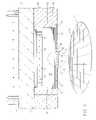
- FIG. 1shows a side cross-sectional view of a prior art probe assembly 2 for probing integrated circuit chip 4 which is disposed on surface 6 of support member 8 for integrated circuit chip 4 .
- Probe assembly 2consists of a dielectric substrate 10 having a central aperture 12 therethrough. On surface 14 of substrate 10 there are disposed a plurality of electrically conducting beams which extend towards edge 18 of aperture 12 .
- Conductors 16have ends 20 which bend downwardly in a direction generally perpendicular to the plane of surface 14 of substrate 10 . Tips 22 of downwardly projecting electrically conducting ends 20 are disposed in electrical contact with contact locations 24 on surface 25 of integrated circuit chip 4 .
- Coaxial cables 26bring electrical signals, power and ground through electrical connectors 28 at periphery 30 of substrate 10 . Structure 2 of FIG.
- Conductors 16were generally made of a high strength metal such as tungsten to resist damage from use. Tungsten has an undesirably high resistivity.
- a broad aspect of the present inventionis a test probe having a plurality of electrically conducting elongated members embedded in a material. One end of each conductor is arranged for alignment with contact locations on a workpiece to be tested.
- the other end of the elongated conductorsare electrically connected to contact locations on the surface of a fan-out substrate.
- the fan-out substrateprovides space transformation of the closely spaced electrical contacts on the first side of the fan-out substrate. Contact locations having a larger spacing are on a second side of the fan out substrate.
- pinsare electrically connected to the contact locations on the second surface of the fan out substrate.
- the plurality of pins on the second surface of the fan-out substrateare inserted into a socket on a second fan-out substrate.
- the first and second space transformation substratesprovide fan out from the fine pitch of the integrated circuit I/O to a larger pitch of electrical contacts for providing signal, power and ground to the workpiece to be tested.
- the pin and socket assemblyis replaced by an interposer containing a plurality of elongated electrical connectors embedded in a layer of material which is squeezed between contact locations on the first fan-out substrate and contact locations on the second fan-out substrate.
- the test probeis part of a test apparatus and test tool.
- Another broad aspect of the present inventionis a method of fabricating the probe tip of the probe according to the present invention wherein a plurality of elongated conductors are bonded to contact locations on a substrate surface and project away therefrom.
- the elongated conductorsare wire bonded to contact locations on the substrate surface.
- the wiresproject preferably at a nonorthogonal angle from the contact locations.
- the wiresare bonded to the contact locations on the substrate are embedded in a elastomeric material to form a probe tip for the structure of the present invention.
- the elongated conductorsare embedded in an elastomeric material.
- FIG. 1is a schematic cross-section of a conventional test probe for an integrated circuit device.
- FIG. 2is a schematic diagram of one embodiment of the probe structure of the present invention.
- FIG. 3is a schematic diagram of another embodiment of the probe structure of the present invention.
- FIG. 4is an enlarged view of an elastomeric connector electrically interconnecting two space transformation substrates of the structure of FIG. 2 .
- FIG. 5is an enlarged view of the probe tip within dashed circle 100 of FIG. 2 or 3 .
- FIG. 6shows the probe tip of the structure of FIG. 5 probing an integrated circuit device.
- FIGS. 7-13show the process for making the structure of FIG. 5 .
- FIG. 14shows a probe tip structure within a fan-out substrate.
- FIG. 15shows the elongated conductors of the probe tip fixed by solder protuberances to contact locations on a space transformation substrate.
- FIG. 16shows the elongated conductors of the probe tip fixed by laser weld protuberances to contact locations on a space transformation substrate.
- FIG. 17shows both interposer 76 and probe tip 40 rigidly bonded to a space transformer 60 .
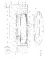
- FIGS. 2 and 3show two embodiments of the test assembly according to the present invention. Numerals common between FIGS. 2 and 3 represent the same thing.
- Probe head 40is formed from a plurality of elongated electrically conducting members 42 embedded in a material 44 which is preferably an elastomeric material 44 .
- the elongated conducting members 42have ends 46 for probing contact locations on integrated circuit devices 48 of wafer 50 .
- the workpieceis an integrated circuit such as a semiconductor chip or a semiconductor wafer having a plurality of chips.
- the workpiececan be any other electronic device.
- the opposite ends 52 of elongated electrical conductors 42are in electrical contact with space transformer (or fan-out substrate) 54 .
- space transformer 54is a multilevel metal/ceramic substrate, a multilevel metal/polymer substrate or a printed circuit board which are typically used as packaging substrates for integrated circuit chips.
- Space transformer 54has, in the preferred embodiment, a surface layer 56 comprising a plurality of thin dielectric films, preferably polymer films such as polyimide, and a plurality of layers of electrical conductors, for example, copper conductors.
- a process for fabricating multilayer structure 56 for disposing it on surface 58 of substrate 60 to form a space transformer 54is described in U.S. patent application Ser. No.
- Pins 64are standard pins used on integrated circuit chip packaging substrates. Pins 64 are inserted into socket 66 or plated through-holes in the substrate 68 which is disposed on surface 70 of second space transformer 68 .
- Socket 66is a type of pin grid array (PGA) socket such as commonly disposed on a printed circuit board of an electronic computer for receiving pins from a packaging substrate.
- Second space transformer 68can be any second level integrated circuit packaging substrate, for example, a standard printed circuit board. Socket 66 is disposed on surface 70 of substrate 68 . On opposite surface 70 of substrate 68 there are disposed a plurality of electrical connectors to which coaxial cables 72 are electrically connected.
- socket 68can be a zero insertion force (ZIF) connector or the socket 68 can be replaced by through-holes in the substrate 68 wherein the through-holes have electrically conductive material surrounding the sidewalls such as a plated through-hole.
- ZIFzero insertion force
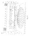
- elastomeric connector 76In the embodiment of FIG. 3 , the pin 64 and socket 66 combination of the embodiment of FIG. 2 is replaced by an interposer, such as, elastomeric connector 76 .
- interposersuch as, elastomeric connector 76 .
- the structure of elastomeric connector 76 and the process for fabricating elastomeric connector 76is described in copending U.S. patent application Ser. No. 07/963,364 to B. Beaman et al., filed Oct. 19, 1992, entitled “THREE DIMENSIONAL HIGH PERFORMANCE INTERCONNECTION MEANS”, which is assigned to the assignee of the present invention, the teaching of which is incorporated herein by reference and of which the present application is a continuation-in-part thereof, the priority date of the filing thereof being claimed herein.
- the elastomeric connectedcan be opted to have one end permanently bonded to the substrate, thus forming a FRU (field replacement unit) together with the probe/sub
- FIG. 4shows a cross-sectional view of structure of the elastomeric connector 76 of FIG. 3 .
- Connector 76is fabricated of preferably elastomeric material 78 having opposing, substantially parallel and planar surfaces 80 and 82 .
- Through elastomeric material 78extending from surface 81 to 83 there are a plurality of elongated electrical conductors 85 .
- Elongated electrical conductors 84are preferably at a nonorthogonal angle to surfaces 81 and 83 .
- Elongated conductors 85are preferably wires which have protuberances 86 at surface 81 of elastomeric material layer 78 and flattened protuberances 88 at surface 83 of elastomeric material layer 78 .
- Flattened protuberances 88preferably have a projection on the flattened surface as shown for the structure of FIG. 14 .
- Protuberance 86is preferably spherical and flattened protuberance 88 is preferably a flattened sphere.
- Connector 76is squeezed between surface 62 of substrate 54 and surface 73 of substrate 68 to provide electrical connection between end 88 of wires 85 and contact location 75 on surface 73 of substrate 68 and between end 88 or wires 85 and contact location 64 on surface 62 of substrate 54 .
- connector 76can be rigidly attached to substrate 54 by solder bonding ends 88 of wires 85 to pads 64 on substrate 54 or by wire bonding ends 86 of wires 85 to pads 64 on substrate 54 in the same manner that wires 42 are bonded to pads 106 as described herein below with respect to FIG. 5 .
- Wires 85can be encased in an elastomeric material in the same manner as wires 42 of FIG. 5 .
- Space transformer 54is held in place with respect to second space transformer 68 by clamping arrangement 80 which is comprised of member 82 which is perpendicularly disposed with respect to surface 70 of second space transformer 68 and member 84 which is preferably parallely disposed with respect to surface 86 of first space transformer 54 .
- Member 84presses against surface 87 of space transformer 54 to hold space transformer 54 in place with respect surface 70 of space transformer 64 .
- Member 82 of clamping arrangement 80can be held in place with respect to surface 70 by a screw which is inserted through member 84 at location 90 extending through the center of member 82 and screw into surface 70 .
- second space transformer 68 and first space transformer with probe head 40is held in place with respect wafer 50 by assembly holder 94 which is part of an integrated circuit test tool or apparatus.
- Assembly holder 94which is part of an integrated circuit test tool or apparatus.
- Members 82 , 84 and 90can be made from materials such as aluminum.
- FIG. 5is a enlarged view of the region of FIGS. 2 or 3 closed in dashed circle 100 which shows the attachment of probe head 40 to substrate 60 of space transformer 54 .
- elongated conductors 42are preferably wires which are at a non-orthogonal angle with respect to surface 87 of substrate 60 .
- At end 102 of wire 42there is preferably a flattened protuberance 104 which is bonded (by wire bonding, solder bonding or any other known bonding technique) to electrically conducting pad 106 on surface 87 of substrate 60 .
- Elastomeric material 44is substantially flush against surface 87 .
- elongated electrically conducting members 42have an end 110 . In the vicinity of end 110 , there is optimally a cavity 112 surrounding end 110 . The cavity is at surface 108 in the elastomeric material 44 .
- FIG. 6shows the structure of FIG. 5 used to probe integrated circuit chip 114 which has a plurality of contact locations 116 shown as spheres such as a C4 solder balls.
- the ends 110 of conductors 42are pressed in contact with contact locations 116 for the purpose of electrically probing integrated circuit 114 .
- Cavity 112provides an opening in elastomeric material 44 to permit ends 110 to be pressed towards and into solder mounds 116 .
- Cavity 112provides a means for solder mounds 116 to self align to ends 110 and provides a means containing solder mounds which may melt, seep or be less viscous when the probe is operated at an elevated temperature. When the probe is used to test or burn-in workpieces have flat pads as contact locations the cavities 112 can remain or be eliminated.
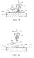
- FIGS. 7-13show the process for fabricating the structure of FIG. 5 .
- Substrate 60 with contact locations 106 thereonis disposed in a wire bound tool.
- the top surface 122 of pad 106is coated by a method such as evaporation, sputtering or plating with soft gold or Ni/Au to provide a suitable surface for thermosonic ball bonding.
- Other bonding techniquescan be used such as thermal compression bonding, ultrasonic bonding, laser bonding and the like.
- a commonly used automatic wire bonderis modified to ball bond gold, gold alloy, copper, copper alloy, aluminum, Pt, nickel or palladium wires 120 to the pad 106 on surface 122 as shown in FIG. 7 .
- the wirepreferably has a diameter of 0.001 to 0.005 inches.
- Structure 124 of FIG. 7is the ball bonding head which has a wire 126 being fed from a reservoir of wire as in a conventional wire bonding apparatus.
- FIG. 7shows the ball bond head 124 in contact at location 426 with surface 122 of pad 106 .
- FIG. 8shows the ball bonding head 124 withdrawn in the direction indicated by arrow 128 from the pad 106 and the wire 126 drawn out to leave disposed on the pad 106 surface 122 wire 130 .
- the bond head 124is stationary and the substrate 60 is advanced as indicated by arrow 132 .
- the bond wireis positioned at an angle preferably between 5 to 60° from vertical and then mechanically notched (or nicked) by knife edge 134 as shown in FIG. 9 .
- the knife edge 134is actuated, the wire 126 is clamped and the bond head 124 is raised. The wire is pulled up and breaks at the notch or nick.
- each wireis ball bonded to adjacent contact locations which can be spaced less than 5 mils apart.
- the wireis held tight and knife edge 134 notches the wire leaving upstanding or flying leads 120 bonded to contact locations 106 in a dense array.
- FIG. 10shows the wire 126 notched (or nicked) to leave wire 120 disposed on surface 122 of pad 106 .
- the wire bond head 124is retracted upwardly as indicated by arrow 136 .
- the wire bond head 124has a mechanism to grip and release wire 126 so that wire 126 can be tensioned against the shear blade to sever the wire.
- a casting mold 140 as shown in FIG. 11is disposed on surface 142 of substrate 60 .
- the moldis a tubular member of any cross-sectional shape, such as circular and polygonal.
- the moldis preferably made of metal or organic materials.
- the length of the moldis preferably the height 144 os the wirse 120 .
- a controlled volume of liquid elastomer 146is disposed into the casting 140 mold and allowed to settle out (flow between the wires until the surface is level) before curing as shown in FIG. 13 .
- the moldis removed to provide the structure shown in FIG. 5 except for cavities 112 .
- the cured elastomeris represented by reference numeral 44 .
- a mold enclosing the wires 120can be used so that the liquid elastomer can be injection molded to encase the wires 120 .
- the top surface of the composite polymer/wire blockan be mechanically planarized to provide a uniform wire height and smooth polymer surface.
- a moly mask with holes located over the ends of the wire contactsis used to selectively ablate (or reactive ion etch) a cup shaped recess in the top surface of the polymer around each of the wires.
- the probe contactscan be reworked by repeating the last two process steps.
- a high compliance, high thermal stability siloxane elastomer materialis preferable for this application.
- the compliance of the cured elastomeris selected for the probe application. Where solder mounds are probed a more rigid elastomeric is used so that the probe tips are pushed into the solder mounds where a gold coated aluminum pad is being probed a more compliant elastomeric material is used to permit the wires to flex under pressure so that good electrical contact is made therewith.
- the high temperature siloxane materialis cast or injected and cured similar to other elastomeric materials. To minimize the shrinkage, the elastomer is preferably cured at lower temperature (T ⁇ 60°) followed by complete cure at higher temperatures (T ⁇ 80°).
- the use of polydimethylsiloxane based rubbersbest satisfy both the material and processing requirements.
- the thermal stability of such elastomersis limited at temperatures below 200° C. and significant outgassing is observed above 100° C.
- the thermal stabilitycan be significantly enhanced by the incorporation of 25 wt % or more diphenylsiloxane.
- enhancement in the thermal stabilityhas been demonstrated by increasing the molecular weight of the resins (oligomers) or minimizing the cross-link junction. The outgassing of the elastomers can be minimized at temperatures below 300° C.
- the high density test probeprovides a means for testing high density and high performance integrated circuits in wafer form or as discrete chips.
- the probe contactscan be designed for high performance functional testing or high temperature burn-in applications.
- the probe contactscan also be reworked several times by resurfacing the rigid polymer material that encases the wires exposing the ends of the contacts.
- the high density probe contacts described in this disclosureare designed to be used for testing semiconductor devices in either wafer form or as discrete chips.
- the high density probeuses metal wires that are bonded to a rigid substrate.
- the wiresare imbedded in a rigid polymer that has a cup shaped recess around each to the wire ends.
- the cup shaped recess 112 shown in FIG. 5provides a positive self-aligning function for chips with solder ball contacts.
- a plurality of probe heads 40can be mounted onto a space transformation substrate 60 so that a plurality of chips can be probed an burned-in simultaneously.
- An alternate embodiment of this inventionwould include straight wires instead of angled wires.
- Another alternate embodimentcould use a suspended alignment mask for aligning the chip to the wire contacts instead of the cup shaped recesses in the top surface of the rigid polymer.
- the suspended alignment maskis made by ablating holes in a thin sheet of polyimide using an excimer laser and a metal mask with the correct hole pattern.
- Another alternate embodiment of this designwould include a interposer probe assembly that could be made separately from the test substrate as described in U.S. patent application, Ser. No. 07/963,364, incorporated by reference herein above.
- This designcould be fabricated by using a copper substrate that would be etched away after the probe assembly is completed and the polymer is cured. This approach could be further modified by using an adhesion de-promoter on the wirse to allow them to slide freely (along the axis of the wires) in the polymer material.
- FIG. 14shows an alternate embodiment of probe tip 40 of FIGS. 2 and 3 .
- probe tip 40is fabricated to be originally fixed to the surface of a first level space transformer 54 .
- Each wire 120is wire bonded directly to a pad 106 on substrate 60 so that the probe assembly 40 is rigidly fixed to the substrate 60 .
- the probe head assembly 40can be fabricated via a discrete stand alone element. This can be fabricated following the process of U.S. patent application Ser. No. 07/963,348, filed Oct. 19, 1992, which has been incorporated herein by reference above. Following this fabrication process as described herein above, wires 42 of FIG. 14 are wire bonded to a surface.
- wire 42is wire bonded to a sacrificial substrate as described in the application incorporated herein.
- the sacrificial substrateis removed to leave the structure of FIG. 14 .
- the sacrificial substrate to which the wires are bondedhave an array of pits which result in a protrusion 150 which can have any predetermined shape such as a hemisphere or a pyramid.
- Protrusion 150provides a raised contact for providing good electrical connection to a contact location against which is pressed.
- probe tip assembly 40can be pressed towards surface 58 of substrate 60 so that ends 104 of FIG. 14 can be pressed against contact locations such as 106 of FIG. 5 on substrate 60 .
- Protuberances 104are aligned to pads 100 on surface 58 of FIG. 5 in a manner similar to how the conductor ends 86 and 88 of the connector in FIG. 4 are aligned to pads 75 and 64 respectively.
- wire 126is ball bonded to pad 106 on substrate 60 .
- An alternative processis to start with a substrate 160 as shown in FIG. 15 having contact locations 162 having an electrically conductive material 164 disposed on surface 166 of contact location 162 .
- Electrically conductive material 164can be solder.
- a bond lead such as 124 of FIG. 7can be used to dispose end 168 of wire 170 against solder mound 164 which can be heated to melting. End 168 of wire 170 is pressed into the molten solder mound to form wire 172 embedded into a solidified solder mound 174 .
- Using this processa structure similar to that of FIG. 5 can be fabricated.
- FIG. 16shows another alternative embodiment of a method to fabricate the structure of FIG. 5 .
- End 180 elongated electrical conductor 182is held against top surface 163 of pad 162 on substrate 160 .
- a beam of light 184 from laser 186is directed at end 180 of elongated conductor 182 at the location of contact with surface 163 of pad 162 .
- the end 180is laser welded to surface 163 to form protuberance 186 .
- the present inventionis directed to high density test probe for testing high density and high performance integrated circuits in wafer form or as discrete chips.
- the probe contactsare designed for high performance functional testing and for high temperature burn in applications.
- the probeis formed from an elastomeric probe tip having a highly dense array of elongated electrical conductors embedded in an elastomeric material which is in electrical contact with a space transformer.
Landscapes
- Physics & Mathematics (AREA)
- General Physics & Mathematics (AREA)
- Engineering & Computer Science (AREA)
- Power Engineering (AREA)
- Measuring Leads Or Probes (AREA)
- Testing Or Measuring Of Semiconductors Or The Like (AREA)
Abstract
Description
- This invention relates to an apparatus and test probe for integrated circuit devices and methods of use thereof.
- In the microelectronics industry, before integrated circuit (IC) chips are packaged in an electronic component, such as a computer, they are tested. Testing is essential to determine whether the integrated circuit's electrical characteristics conform to the specifications to which they were designed to ensure that electronic component performs the function for which is was designed.
- Testing is an expensive part of the fabrication process of contemporary computing systems. The functionality of every I/O for contemporary integrated circuit must be tested since a failure to achieve the design specification at a single I/O can render an integrated circuit unusable for a specific application. The testing is commonly done both at room temperature and at elevated temperatures to test functionality and at elevated temperatures with forced voltages and currents to bum the chips in and to test the reliability of the integrated circuit to screen out early failures.
- Contemporary probes for integrated circuits are expensive to fabricate and are easily damaged. Contemporary test probes are typically fabricated on a support substrate from groups of elongated metal conductors which fan inwardly towards a central location where each conductor has an end which corresponds to a contact location on the integrated circuit chip to be tested. The metal conductors generally cantilever over an aperture in the support substrate. The wires are generally fragile and easily damage and are easily displaceable from the predetermined positions corresponding to the design positions of the contact locations on the integrated circuit being tested. These probes last only a certain number of testing operations, after which they must be replaced by an expensive replacement or reworked to recondition the probes.
FIG. 1 shows a side cross-sectional view of a priorart probe assembly 2 for probing integrated circuit chip4 which is disposed onsurface 6 ofsupport member 8 for integrated circuit chip4.Probe assembly 2 consists of adielectric substrate 10 having acentral aperture 12 therethrough. Onsurface 14 ofsubstrate 10 there are disposed a plurality of electrically conducting beams which extend towardsedge 18 ofaperture 12.Conductors 16 haveends 20 which bend downwardly in a direction generally perpendicular to the plane ofsurface 14 ofsubstrate 10.Tips 22 of downwardly projecting electrically conductingends 20 are disposed in electrical contact withcontact locations 24 onsurface 25 of integrated circuit chip4.Coaxial cables 26 bring electrical signals, power and ground throughelectrical connectors 28 atperiphery 30 ofsubstrate 10.Structure 2 ofFIG. 1 has the disadvantage of being expensive to fabricate and of having fragileinner ends 20 ofelectrical conductors 16. Ends20 are easily damaged through use in probing electronic devices. Since theprobe 2 is expensive to fabricate, replacement adds a substantial cost to the testing of integrated circuit devices.Conductors 16 were generally made of a high strength metal such as tungsten to resist damage from use. Tungsten has an undesirably high resistivity.- It is an object of the present invention to provide an improved high density test probe, test apparatus and method of use thereof.
- It is another object of the present invention to provide an improved test probe for testing and burning-in integrated circuits.
- It is another object of the present invention to provide an improved test probe and apparatus for testing integrated circuits in wafer form and as discrete integrated circuit chips.
- It is an additional object of the present invention to provide probes having contacts which can be designed for high performance functional testing and for high temperature burn in applications.
- It is yet another object of the present invention to provide probes having contacts which can be reworked several times by resurfacing some of the materials used to fabricate the probe of the present invention.
- It is a further object of the present invention to provide an improved test probe having a probe tip member containing a plurality of elongated conductors each ball bonded to electrical contact locations on space transformation substrate.
- A broad aspect of the present invention is a test probe having a plurality of electrically conducting elongated members embedded in a material. One end of each conductor is arranged for alignment with contact locations on a workpiece to be tested.
- In a more particular aspect of the present invention, the other end of the elongated conductors are electrically connected to contact locations on the surface of a fan-out substrate. The fan-out substrate provides space transformation of the closely spaced electrical contacts on the first side of the fan-out substrate. Contact locations having a larger spacing are on a second side of the fan out substrate.
- In yet another more particular aspect of the present invention, pins are electrically connected to the contact locations on the second surface of the fan out substrate.
- In another more particular aspect of the present invention, the plurality of pins on the second surface of the fan-out substrate are inserted into a socket on a second fan-out substrate. The first and second space transformation substrates provide fan out from the fine pitch of the integrated circuit I/O to a larger pitch of electrical contacts for providing signal, power and ground to the workpiece to be tested.
- In another more particular aspect of the present invention, the pin and socket assembly is replaced by an interposer containing a plurality of elongated electrical connectors embedded in a layer of material which is squeezed between contact locations on the first fan-out substrate and contact locations on the second fan-out substrate.
- In another more particular aspect of the present invention, the test probe is part of a test apparatus and test tool.
- Another broad aspect of the present invention is a method of fabricating the probe tip of the probe according to the present invention wherein a plurality of elongated conductors are bonded to contact locations on a substrate surface and project away therefrom.
- In a more particular aspect of the method according to the present invention, the elongated conductors are wire bonded to contact locations on the substrate surface. The wires project preferably at a nonorthogonal angle from the contact locations.
- In another more particular aspect of the method of the present invention, the wires are bonded to the contact locations on the substrate are embedded in a elastomeric material to form a probe tip for the structure of the present invention.
- In another more particular aspect of the present invention, the elongated conductors are embedded in an elastomeric material.
FIG. 1 is a schematic cross-section of a conventional test probe for an integrated circuit device.FIG. 2 is a schematic diagram of one embodiment of the probe structure of the present invention.FIG. 3 is a schematic diagram of another embodiment of the probe structure of the present invention.FIG. 4 is an enlarged view of an elastomeric connector electrically interconnecting two space transformation substrates of the structure ofFIG. 2 .FIG. 5 is an enlarged view of the probe tip withindashed circle 100 ofFIG. 2 or3.FIG. 6 shows the probe tip of the structure ofFIG. 5 probing an integrated circuit device.FIGS. 7-13 show the process for making the structure ofFIG. 5 .FIG. 14 shows a probe tip structure within a fan-out substrate.FIG. 15 shows the elongated conductors of the probe tip fixed by solder protuberances to contact locations on a space transformation substrate.FIG. 16 shows the elongated conductors of the probe tip fixed by laser weld protuberances to contact locations on a space transformation substrate.FIG. 17 shows bothinterposer 76 andprobe tip 40 rigidly bonded to aspace transformer 60.- Turning now to the Figures,
FIGS. 2 and 3 show two embodiments of the test assembly according to the present invention. Numerals common betweenFIGS. 2 and 3 represent the same thing.Probe head 40 is formed from a plurality of elongated electrically conductingmembers 42 embedded in amaterial 44 which is preferably anelastomeric material 44. The elongated conductingmembers 42 haveends 46 for probing contact locations on integratedcircuit devices 48 ofwafer 50. In the preferred embodiment, the workpiece is an integrated circuit such as a semiconductor chip or a semiconductor wafer having a plurality of chips. The workpiece can be any other electronic device. The opposite ends52 of elongatedelectrical conductors 42 are in electrical contact with space transformer (or fan-out substrate)54. In the preferred embodiment,space transformer 54 is a multilevel metal/ceramic substrate, a multilevel metal/polymer substrate or a printed circuit board which are typically used as packaging substrates for integrated circuit chips.Space transformer 54 has, in the preferred embodiment, asurface layer 56 comprising a plurality of thin dielectric films, preferably polymer films such as polyimide, and a plurality of layers of electrical conductors, for example, copper conductors. A process for fabricatingmultilayer structure 56 for disposing it onsurface 58 ofsubstrate 60 to form aspace transformer 54 is described in U.S. patent application Ser. No. 07/695,368, filed on May 3, 1991, entitled “MULTI-LAYER THIN FILM STRUCTURE AND PARALLEL PROCESSING METHOD FOR FABRICATING SAME” which is assigned to the assignee of the present invention, the teaching of which is incorporated herein by reference. Details of the fabrication ofprobe head 40 and of the assembly ofprobe head - As shown in
FIG. 2 , onsurface 62 ofsubstrate 60, there are, a plurality ofpins 64.Surface 62 is opposite the surface57 on whichprobe head 40 is disposed. Pins 64 are standard pins used on integrated circuit chip packaging substrates.Pins 64 are inserted intosocket 66 or plated through-holes in thesubstrate 68 which is disposed onsurface 70 ofsecond space transformer 68.Socket 66 is a type of pin grid array (PGA) socket such as commonly disposed on a printed circuit board of an electronic computer for receiving pins from a packaging substrate.Second space transformer 68 can be any second level integrated circuit packaging substrate, for example, a standard printed circuit board.Socket 66 is disposed onsurface 70 ofsubstrate 68. Onopposite surface 70 ofsubstrate 68 there are disposed a plurality of electrical connectors to whichcoaxial cables 72 are electrically connected. Alternatively,socket 68 can be a zero insertion force (ZIF) connector or thesocket 68 can be replaced by through-holes in thesubstrate 68 wherein the through-holes have electrically conductive material surrounding the sidewalls such as a plated through-hole.- In the embodiment of
FIG. 3 , thepin 64 andsocket 66 combination of the embodiment ofFIG. 2 is replaced by an interposer, such as,elastomeric connector 76. The structure ofelastomeric connector 76 and the process for fabricatingelastomeric connector 76 is described in copending U.S. patent application Ser. No. 07/963,364 to B. Beaman et al., filed Oct. 19, 1992, entitled “THREE DIMENSIONAL HIGH PERFORMANCE INTERCONNECTION MEANS”, which is assigned to the assignee of the present invention, the teaching of which is incorporated herein by reference and of which the present application is a continuation-in-part thereof, the priority date of the filing thereof being claimed herein. The elastomeric connected can be opted to have one end permanently bonded to the substrate, thus forming a FRU (field replacement unit) together with the probe/substrate/connector assembly. FIG. 4 shows a cross-sectional view of structure of theelastomeric connector 76 ofFIG. 3 .Connector 76 is fabricated of preferablyelastomeric material 78 having opposing, substantially parallel andplanar surfaces elastomeric material 78, extending fromsurface 81 to83 there are a plurality of elongatedelectrical conductors 85. Elongatedelectrical conductors 84 are preferably at a nonorthogonal angle tosurfaces Elongated conductors 85 are preferably wires which haveprotuberances 86 atsurface 81 ofelastomeric material layer 78 and flattenedprotuberances 88 atsurface 83 ofelastomeric material layer 78. Flattenedprotuberances 88 preferably have a projection on the flattened surface as shown for the structure ofFIG. 14 .Protuberance 86 is preferably spherical and flattenedprotuberance 88 is preferably a flattened sphere.Connector 76 is squeezed betweensurface 62 ofsubstrate 54 andsurface 73 ofsubstrate 68 to provide electrical connection betweenend 88 ofwires 85 andcontact location 75 onsurface 73 ofsubstrate 68 and betweenend 88 orwires 85 andcontact location 64 onsurface 62 ofsubstrate 54.- Alternatively, as shown in
FIG. 17 ,connector 76 can be rigidly attached tosubstrate 54 by solder bonding ends88 ofwires 85 topads 64 onsubstrate 54 or by wire bonding ends86 ofwires 85 topads 64 onsubstrate 54 in the same manner thatwires 42 are bonded topads 106 as described herein below with respect toFIG. 5 .Wires 85 can be encased in an elastomeric material in the same manner aswires 42 ofFIG. 5 . Space transformer 54 is held in place with respect tosecond space transformer 68 by clampingarrangement 80 which is comprised ofmember 82 which is perpendicularly disposed with respect to surface70 ofsecond space transformer 68 andmember 84 which is preferably parallely disposed with respect to surface86 offirst space transformer 54.Member 84 presses againstsurface 87 ofspace transformer 54 to holdspace transformer 54 in place withrespect surface 70 ofspace transformer 64.Member 82 of clampingarrangement 80 can be held in place with respect to surface70 by a screw which is inserted throughmember 84 atlocation 90 extending through the center ofmember 82 and screw intosurface 70.- The entire assembly of
second space transformer 68 and first space transformer withprobe head 40 is held in place withrespect wafer 50 byassembly holder 94 which is part of an integrated circuit test tool or apparatus.Members FIG. 5 is a enlarged view of the region ofFIGS. 2 or3 closed in dashedcircle 100 which shows the attachment ofprobe head 40 tosubstrate 60 ofspace transformer 54. In the preferred embodiment,elongated conductors 42 are preferably wires which are at a non-orthogonal angle with respect to surface87 ofsubstrate 60. Atend 102 ofwire 42 there is preferably a flattenedprotuberance 104 which is bonded (by wire bonding, solder bonding or any other known bonding technique) to electrically conductingpad 106 onsurface 87 ofsubstrate 60.Elastomeric material 44 is substantially flush againstsurface 87. At substantially oppositely disposedplanar surface 108 elongated electrically conductingmembers 42 have anend 110. In the vicinity ofend 110, there is optimally acavity 112surrounding end 110. The cavity is atsurface 108 in theelastomeric material 44.FIG. 6 shows the structure ofFIG. 5 used to probe integratedcircuit chip 114 which has a plurality of contact locations116 shown as spheres such as a C4 solder balls. The ends110 ofconductors 42 are pressed in contact with contact locations116 for the purpose of electrically probingintegrated circuit 114.Cavity 112 provides an opening inelastomeric material 44 to permit ends110 to be pressed towards and into solder mounds116.Cavity 112 provides a means for solder mounds116 to self align toends 110 and provides a means containing solder mounds which may melt, seep or be less viscous when the probe is operated at an elevated temperature. When the probe is used to test or burn-in workpieces have flat pads as contact locations thecavities 112 can remain or be eliminated.FIGS. 7-13 show the process for fabricating the structure ofFIG. 5 .Substrate 60 withcontact locations 106 thereon is disposed in a wire bound tool. Thetop surface 122 ofpad 106 is coated by a method such as evaporation, sputtering or plating with soft gold or Ni/Au to provide a suitable surface for thermosonic ball bonding. Other bonding techniques can be used such as thermal compression bonding, ultrasonic bonding, laser bonding and the like. A commonly used automatic wire bonder is modified to ball bond gold, gold alloy, copper, copper alloy, aluminum, Pt, nickel orpalladium wires 120 to thepad 106 onsurface 122 as shown inFIG. 7 . The wire preferably has a diameter of 0.001 to 0.005 inches. If a metal other than Au is used, a thin passivation metal such as Au, Cr, Co, Ni or Pd can be coated over the wire by means of electroplating, or electroless plating, sputtering, e-beam evaporation or any other coating techniques known in the industry.Structure 124 ofFIG. 7 is the ball bonding head which has awire 126 being fed from a reservoir of wire as in a conventional wire bonding apparatus.FIG. 7 shows theball bond head 124 in contact at location426 withsurface 122 ofpad 106.FIG. 8 shows theball bonding head 124 withdrawn in the direction indicated byarrow 128 from thepad 106 and thewire 126 drawn out to leave disposed on thepad 106surface 122wire 130. In the preferred embodiment, thebond head 124 is stationary and thesubstrate 60 is advanced as indicated byarrow 132. The bond wire is positioned at an angle preferably between 5 to 60° from vertical and then mechanically notched (or nicked) byknife edge 134 as shown inFIG. 9 . Theknife edge 134 is actuated, thewire 126 is clamped and thebond head 124 is raised. The wire is pulled up and breaks at the notch or nick.- Cutting the
wire 130 while it is suspended is not done in conventional wire bonding. In conventional wire bonding, such as that used to fabricate the electrical connector of U.S. Pat. No. 4,998,885, where, as shown inFIG. 8 thereof, one end a wire is ball bonded using a wire bonded to a contact location on a substrate bent over a loop post and the other of the wire is wedge bonded to an adjacent contact location on the substrate. The loop is severed by a laser as shown inFIG. 6 and the ends melted to form balls. This process results in adjacent contact locations having different types of bonds, one a ball bond the other a wedge bond. The spacing of the adjacent pads cannot be less than about about 20 mils because of the need to bond the wire. This spacing is unacceptable to fabricate a high density probe tip since dense integrated circuits have pad spacing less than this amount. In contradistinction, according to the present invention, each wire is ball bonded to adjacent contact locations which can be spaced less than 5 mils apart. The wire is held tight andknife edge 134 notches the wire leaving upstanding or flying leads120 bonded to contactlocations 106 in a dense array. - When the
wire 130 is severed there is left on thesurface 122 ofpad 106 an angled flyinglead 120 which is bonded to surface122 at one end and the other end projects outwardly away from the surface. A ball can be formed on the end of thewire 130 which is not bonded to surface122 using a laser or electrical discharge to melt the end of the wire. Techniques for this are described in copending U.S. patent application Ser. No. 07/963,346, filed Oct. 19, 1992, which is incorporated herein by reference above. FIG. 10 shows thewire 126 notched (or nicked) to leavewire 120 disposed onsurface 122 ofpad 106. Thewire bond head 124 is retracted upwardly as indicated byarrow 136. Thewire bond head 124 has a mechanism to grip andrelease wire 126 so thatwire 126 can be tensioned against the shear blade to sever the wire.- After the wire bonding process is completed, a casting
mold 140 as shown inFIG. 11 is disposed onsurface 142 ofsubstrate 60. The mold is a tubular member of any cross-sectional shape, such as circular and polygonal. The mold is preferably made of metal or organic materials. The length of the mold is preferably theheight 144 os thewirse 120. A controlled volume ofliquid elastomer 146 is disposed into the casting140 mold and allowed to settle out (flow between the wires until the surface is level) before curing as shown inFIG. 13 . Once the elastomer has cured, the mold is removed to provide the structure shown inFIG. 5 except forcavities 112. The cured elastomer is represented byreference numeral 44. A mold enclosing thewires 120 can be used so that the liquid elastomer can be injection molded to encase thewires 120. - The top surface of the composite polymer/wire block an be mechanically planarized to provide a uniform wire height and smooth polymer surface. A moly mask with holes located over the ends of the wire contacts is used to selectively ablate (or reactive ion etch) a cup shaped recess in the top surface of the polymer around each of the wires. The probe contacts can be reworked by repeating the last two process steps.
- A high compliance, high thermal stability siloxane elastomer material is preferable for this application. The compliance of the cured elastomer is selected for the probe application. Where solder mounds are probed a more rigid elastomeric is used so that the probe tips are pushed into the solder mounds where a gold coated aluminum pad is being probed a more compliant elastomeric material is used to permit the wires to flex under pressure so that good electrical contact is made therewith. The high temperature siloxane material is cast or injected and cured similar to other elastomeric materials. To minimize the shrinkage, the elastomer is preferably cured at lower temperature (T≦60°) followed by complete cure at higher temperatures (T≧80°).
- Among the many commercially available elastomers, such as ECCOSIL and SYLGARD, the use of polydimethylsiloxane based rubbers best satisfy both the material and processing requirements. However, the thermal stability of such elastomers is limited at temperatures below 200° C. and significant outgassing is observed above 100° C. We have found that the thermal stability can be significantly enhanced by the incorporation of 25 wt % or more diphenylsiloxane. Further, enhancement in the thermal stability has been demonstrated by increasing the molecular weight of the resins (oligomers) or minimizing the cross-link junction. The outgassing of the elastomers can be minimized at temperatures below 300° C. by first using a thermally transient catalyst in the resin synthesis and secondly subjecting the resin to a thin film distillation to remove low molecular weight side-products. For our experiments, we have found that 25 wt % diphenylsiloxane is optimal, balancing the desired thermal stability with the increased viscosity associated with diphenylsiloxane incorporation. The optimum number average molecular weight of the resin for maximum thermal stability was found to be between 18,000 and 35,000 g/mol. Higher molecular weights were difficult to cure and too viscous, once filled, to process. Network formation was achieved by a standard hydrosilylation polymerization using a hindered platinum catalyst in a reactive silicon oil carrier.
- In
FIG. 10 whenbond head 124 bonds thewire 126 to thesurface 122 ofpad 106 there is formed a flattened spherical end shown as104 inFIG. 6 . - The high density test probe provides a means for testing high density and high performance integrated circuits in wafer form or as discrete chips. The probe contacts can be designed for high performance functional testing or high temperature burn-in applications. The probe contacts can also be reworked several times by resurfacing the rigid polymer material that encases the wires exposing the ends of the contacts.
- The high density probe contacts described in this disclosure are designed to be used for testing semiconductor devices in either wafer form or as discrete chips. The high density probe uses metal wires that are bonded to a rigid substrate. The wires are imbedded in a rigid polymer that has a cup shaped recess around each to the wire ends. The cup shaped
recess 112 shown inFIG. 5 provides a positive self-aligning function for chips with solder ball contacts. A plurality of probe heads40 can be mounted onto aspace transformation substrate 60 so that a plurality of chips can be probed an burned-in simultaneously. - An alternate embodiment of this invention would include straight wires instead of angled wires. Another alternate embodiment could use a suspended alignment mask for aligning the chip to the wire contacts instead of the cup shaped recesses in the top surface of the rigid polymer. The suspended alignment mask is made by ablating holes in a thin sheet of polyimide using an excimer laser and a metal mask with the correct hole pattern. Another alternate embodiment of this design would include a interposer probe assembly that could be made separately from the test substrate as described in U.S. patent application, Ser. No. 07/963,364, incorporated by reference herein above. This design could be fabricated by using a copper substrate that would be etched away after the probe assembly is completed and the polymer is cured. This approach could be further modified by using an adhesion de-promoter on the wirse to allow them to slide freely (along the axis of the wires) in the polymer material.
FIG. 14 shows an alternate embodiment ofprobe tip 40 ofFIGS. 2 and 3 . As described herein above,probe tip 40 is fabricated to be originally fixed to the surface of a firstlevel space transformer 54. Eachwire 120 is wire bonded directly to apad 106 onsubstrate 60 so that theprobe assembly 40 is rigidly fixed to thesubstrate 60. The embodiment ofFIG. 14 , theprobe head assembly 40 can be fabricated via a discrete stand alone element. This can be fabricated following the process of U.S. patent application Ser. No. 07/963,348, filed Oct. 19, 1992, which has been incorporated herein by reference above. Following this fabrication process as described herein above,wires 42 ofFIG. 14 are wire bonded to a surface. Rather than being wire bonded directly to a pad on a space transformation substrate,wire 42 is wire bonded to a sacrificial substrate as described in the application incorporated herein. The sacrificial substrate is removed to leave the structure ofFIG. 14 . At ends102 ofwires 44 there is a flattenedball 104 caused by the wire bond operation. In a preferred embodiment the sacrificial substrate to which the wires are bonded have an array of pits which result in aprotrusion 150 which can have any predetermined shape such as a hemisphere or a pyramid.Protrusion 150 provides a raised contact for providing good electrical connection to a contact location against which is pressed. Theclamp assembly 80 ofFIGS. 2 and 3 can be modified so thatprobe tip assembly 40 can be pressed towardssurface 58 ofsubstrate 60 so that ends104 ofFIG. 14 can be pressed against contact locations such as106 ofFIG. 5 onsubstrate 60.Protuberances 104 are aligned topads 100 onsurface 58 ofFIG. 5 in a manner similar to how the conductor ends86 and88 of the connector inFIG. 4 are aligned topads - As shown in the process of
FIGS. 7 to 9 ,wire 126 is ball bonded to pad106 onsubstrate 60. An alternative process is to start with asubstrate 160 as shown inFIG. 15 havingcontact locations 162 having an electricallyconductive material 164 disposed onsurface 166 ofcontact location 162. Electricallyconductive material 164 can be solder. A bond lead such as124 ofFIG. 7 can be used to disposeend 168 ofwire 170 againstsolder mound 164 which can be heated to melting.End 168 ofwire 170 is pressed into the molten solder mound to formwire 172 embedded into a solidifiedsolder mound 174. Using this process a structure similar to that ofFIG. 5 can be fabricated. FIG. 16 shows another alternative embodiment of a method to fabricate the structure ofFIG. 5 .- Numerals common between
FIGS. 15 and 16 represent the same thing.End 180 elongatedelectrical conductor 182 is held againsttop surface 163 ofpad 162 onsubstrate 160. A beam of light184 fromlaser 186 is directed atend 180 ofelongated conductor 182 at the location of contact withsurface 163 ofpad 162. Theend 180 is laser welded to surface163 to formprotuberance 186. - In summary, the present invention is directed to high density test probe for testing high density and high performance integrated circuits in wafer form or as discrete chips. The probe contacts are designed for high performance functional testing and for high temperature burn in applications. The probe is formed from an elastomeric probe tip having a highly dense array of elongated electrical conductors embedded in an elastomeric material which is in electrical contact with a space transformer.
- While the present invention has been described with respect to preferred embodiments, numerous modifications, changes and improvements will occur to those skilled in the art without departing from the spirit and scope of the invention.
Claims (30)
1-201. (canceled)
202. A Probe Assembly, comprising:
a second space transformer having a first surface, a second surface and a first plurality of contact locations on the first surface thereof,
an interconnection structure having a first surface, a second surface, a second plurality of elongated resilient electrical conductors extending from the second surface thereof and a first plurality of elongated resilient electrical conductors extending from the first surface thereof, and
a first space transformer having a first surface, a second surface, a plurality of contact locations disposed on the second surface thereof, and a third plurality of elongated resilient electrical conductors extending from the first surface thereof, wherein:
the second plurality of elongated resilient electrical conductors effect a pressure connection with the contact locations of the second space transformer; and
the first plurality of elongated resilient electrical conductors effect a pressure connection with the contact locations of the first space transformer.
203. A Probe Assembly, according toclaim 202 , wherein:
the third plurality of elongated resilient electrical conductors are electrically interconnected to contact locations on the first surface of the first space transformer.
204. A Probe Assembly, according toclaim 202 , wherein:
the first plurality of elongated resilient electrical conductors are composite electrical interconnection elements.
205. A Probe Assembly, according toclaim 202 , wherein:
the second plurality of elongated resilient electrical conductors are composite electrical interconnection elements.
206. A Probe Assembly, according toclaim 202 , wherein:
the third plurality of elongated resilient electrical conductors are composite electrical interconnection elements.
207. A Probe Assembly, according toclaim 202 , wherein:
one or more of the first plurality of elongated resilient electrical conductors are a composite structure comprising an elongated element and a coating.
208. A Probe Assembly, according toclaim 202 , wherein:
one or more of the second plurality of elongated resilient electrical conductors are a composite structure comprising an elongated element and a coating.
209. A structure, according toclaim 202 , further comprising:
a clamp for holding the first space transformer in place with respect to said second space transformer,
the clamp comprises a sheet of material supported by a member perpendicularly disposed with respect to the second space transformer;
means for affixing the sheet to the member; and
means for urging the first space transformer towards the first surface of the second space transformer.
210. A Probe Assembly, according toclaim 209 , wherein said clamps comprises a sheet made of aluminum.
211. A Probe Assembly, according toclaim 209 , wherein the means for urging the first space transformer comprises:
the sheet of material; and
a screw holding the sheet in place with respect to the member and the second space transformer with the first space transformer captured therebetween.
212. A Probe Assembly, according toclaim 211 , wherein:
said sheet comprises aluminum.
213. A Probe Assembly, according toclaim 211 , further comprising:
a member perpendicularly disposed with respect to the second space transformer for supporting the sheet of material.
214. A Probe Assembly, according toclaim 209 , wherein the clamp comprises means for affixing a sheet of material supported by a member perpendicularly disposed with respect to the second space transformer, the sheet is held in place to the member by a screw forming the clamp to hold the first space transformer in place with respect to the second space transformer.
215. A Probe Assembly, according toclaim 214 , wherein:
the sheet and the member are made of aluminum.
216. A Probe Assembly, according to202, further comprising:
means for aligning of the first space transformer relative to the second space transformer.
217. A Probe Assembly, according toclaim 216 , wherein the means for aligning the first space transformer comprises:
a plurality of pins disposed on the first space transformer.
218. A Probe Assembly, according toclaim 216 , wherein the means for aligning the first space transformer comprises:
a plurality of projections for mating with grooves on the interconnection structure.
219. A Probe Assembly, according toclaim 202 , wherein:
the contact locations are disposed at a first pitch on the second surface of the second space transformer;
the third plurality of elongated resilient electrical conductors are disposed at a second pitch on the first surface of the second space transformer.
220. A Probe Assembly, according toclaim 202 , wherein:
the first plurality of elongated resilient electrical conductors are disposed at a first pitch on the first surface of the interconnection structure;
the second plurality of elongated resilient electrical conductors are disposed at a second pitch on the second surface of the interconnection structure.
221. A Probe Assembly, according toclaim 202 , wherein:
the contact locations are disposed at a first pitch on the second surface of the first space transformer;
the third plurality of elongated resilient electrical conductors are disposed at a second pitch on the first surface of the first space transformer;
the first plurality of elongated resilient electrical conductors are disposed at the first pitch on the first surface of the interconnection structure;
the second plurality of elongated resilient electrical conductors are disposed at the first pitch on the second surface of the interconnection structure.
222. A Probe Assembly, according toclaim 202 , wherein at least some of the elongated resilient electrical conductors comprise:
a composite interconnection element having an end; and
a tip structure disposed at the end of the composite interconnection element.
223. A structure, according toclaim 202 , wherein:
the third plurality of elongated resilient electrical conductors are electrically interconnected to contact locations on the first surface of the first space transformer.
224-243. (canceled)
244. A Probe Assembly, according toclaim 219 , wherein the first pitch is greater than the second pitch.
245. A Probe Assembly, according toclaim 220 , wherein the first pitch is substantially the same as the second pitch.
246. A Probe Assembly, according toclaim 221 , wherein the first pitch is greater than the second pitch.
247-314. (canceled)
315. A Probe Assembly, according toclaim 202 , wherein:
the interconnection structure comprises a dielectric material comprising a plurality of elongated electrical conductors embedded therein:
a plurality of first ends of which comprise the first plurality of elongated resilient electrical conductors and a plurality of second ends of which comprise the second plurality of elongated resilient electrical conductors.
316-597. (canceled)
Priority Applications (1)
| Application Number | Priority Date | Filing Date | Title |
|---|---|---|---|
| US12/548,528US20090315579A1 (en) | 1992-10-19 | 2009-08-27 | High density integrated circuit apparatus, test probe and methods of use thereof |
Applications Claiming Priority (6)
| Application Number | Priority Date | Filing Date | Title |
|---|---|---|---|
| US07/963,346US5371654A (en) | 1992-10-19 | 1992-10-19 | Three dimensional high performance interconnection package |
| US08/754,869US5821763A (en) | 1992-10-19 | 1996-11-22 | Test probe for high density integrated circuits, methods of fabrication thereof and methods of use thereof |
| US08/872,519US6334247B1 (en) | 1992-10-19 | 1997-06-11 | High density integrated circuit apparatus, test probe and methods of use thereof |
| US09/921,867US20070271781A9 (en) | 1992-10-19 | 2001-08-03 | High density integrated circuit apparatus, test probe and methods of use thereof |
| US10/408,200US20050062492A1 (en) | 2001-08-03 | 2003-04-04 | High density integrated circuit apparatus, test probe and methods of use thereof |
| US12/548,528US20090315579A1 (en) | 1992-10-19 | 2009-08-27 | High density integrated circuit apparatus, test probe and methods of use thereof |
Related Parent Applications (1)
| Application Number | Title | Priority Date | Filing Date |
|---|---|---|---|
| US10/408,200DivisionUS20050062492A1 (en) | 1992-10-19 | 2003-04-04 | High density integrated circuit apparatus, test probe and methods of use thereof |
Publications (1)
| Publication Number | Publication Date |
|---|---|
| US20090315579A1true US20090315579A1 (en) | 2009-12-24 |
Family
ID=34314301
Family Applications (44)
| Application Number | Title | Priority Date | Filing Date |
|---|---|---|---|
| US10/408,200AbandonedUS20050062492A1 (en) | 1992-10-19 | 2003-04-04 | High density integrated circuit apparatus, test probe and methods of use thereof |
| US11/929,899AbandonedUS20080106282A1 (en) | 1992-10-19 | 2007-10-30 | High density integrated circuit apparatus, test probe and methods of use thereof |
| US11/929,944AbandonedUS20080123310A1 (en) | 1992-10-19 | 2007-10-30 | High density integrated circuit apparatus, test probe and methods of use thereof |
| US11/929,924AbandonedUS20080116916A1 (en) | 1992-10-19 | 2007-10-30 | High density integrated circuit apparatus, test probe and methods of use thereof |
| US11/929,711AbandonedUS20080116912A1 (en) | 1992-10-19 | 2007-10-30 | High density integrated circuit apparatus, test probe and methods of use thereof |
| US11/929,982AbandonedUS20080106284A1 (en) | 1992-10-19 | 2007-10-30 | High density integrated circuit apparatus, test probe and methods of use thereof |
| US11/929,754AbandonedUS20080106281A1 (en) | 1992-10-19 | 2007-10-30 | High density integrated circuit apparatus, test probe and methods of use thereof |
| US11/929,676AbandonedUS20080111568A1 (en) | 1992-10-19 | 2007-10-30 | High density integrated circuit apparatus, test probe and methods of use thereof |
| US11/929,783AbandonedUS20080100318A1 (en) | 1992-10-19 | 2007-10-30 | High density integrated circuit apparatus, test probe and methods of use thereof |
| US11/930,010AbandonedUS20080048691A1 (en) | 1992-10-19 | 2007-10-30 | High density integrated circuit apparatus, test probe and methods of use thereof |
| US11/929,821AbandonedUS20080116915A1 (en) | 1992-10-19 | 2007-10-30 | High density integrated circuit apparatus, test probe and methods of use thereof |
| US11/930,019AbandonedUS20080106285A1 (en) | 1992-10-19 | 2007-10-30 | High density integrated circuit apparatus, test probe and methods of use thereof |
| US11/929,934AbandonedUS20080112144A1 (en) | 1992-10-19 | 2007-10-30 | High density integrated circuit apparatus, test probe and methods of use thereof |
| US11/929,873AbandonedUS20080048690A1 (en) | 1992-10-19 | 2007-10-30 | High density integrated circuit apparatus, test probe and methods of use thereof |
| US11/930,016AbandonedUS20080112149A1 (en) | 1992-10-19 | 2007-10-30 | High density integrated circuit apparatus, test probe and methods of use thereof |
| US11/929,662AbandonedUS20080100317A1 (en) | 1992-10-19 | 2007-10-30 | High density integrated circuit apparatus, test probe and methods of use thereof |
| US11/929,911AbandonedUS20080111570A1 (en) | 1992-10-19 | 2007-10-30 | High density integrated circuit apparatus, test probe and methods of use thereof |
| US11/929,839AbandonedUS20080129320A1 (en) | 1992-10-19 | 2007-10-30 | High density integrated circuit apparatus, test probe and methods of use thereof |
| US11/929,956AbandonedUS20080112145A1 (en) | 1992-10-19 | 2007-10-30 | High density integrated circuit apparatus, test probe and methods of use thereof |
| US11/929,968AbandonedUS20080112147A1 (en) | 1992-10-19 | 2007-10-30 | High density integrated circuit apparatus, test probe and methods of use thereof |
| US11/930,045AbandonedUS20080106872A1 (en) | 1992-10-19 | 2007-10-30 | High density integrated circuit apparatus, test probe and methods of use thereof |
| US11/929,768AbandonedUS20080116913A1 (en) | 1992-10-19 | 2007-10-30 | High density integrated circuit apparatus, test probe and methods of use thereof |
| US11/930,026AbandonedUS20080047741A1 (en) | 1992-10-19 | 2007-10-30 | High density integrated circuit apparatus, test probe and methods of use thereof |
| US11/929,634AbandonedUS20080100316A1 (en) | 1992-10-19 | 2007-10-30 | High density integrated circuit apparatus, test probe and methods of use thereof |
| US11/929,697AbandonedUS20080111569A1 (en) | 1992-10-19 | 2007-10-30 | High density integrated circuit apparatus, test probe and methods of use thereof |
| US11/929,991AbandonedUS20080117612A1 (en) | 1992-10-19 | 2007-10-30 | High density integrated circuit apparatus, test probe and methods of use thereof |
| US11/929,736AbandonedUS20080100324A1 (en) | 1992-10-19 | 2007-10-30 | High density integrated circuit apparatus, test probe and methods of use thereof |
| US11/929,999AbandonedUS20080112148A1 (en) | 1992-10-19 | 2007-10-30 | High density integrated circuit apparatus, test probe and methods of use thereof |
| US11/929,806AbandonedUS20080116914A1 (en) | 1992-10-19 | 2007-10-30 | High density integrated circuit apparatus, test probe and methods of use thereof |
| US11/929,883AbandonedUS20080048697A1 (en) | 1992-10-19 | 2007-10-30 | High density integrated circuit apparatus, test probe and methods of use thereof |
| US11/929,962AbandonedUS20080112146A1 (en) | 1992-10-19 | 2007-10-30 | High density integrated circuit apparatus, test probe and methods of use thereof |
| US11/929,976AbandonedUS20080106283A1 (en) | 1992-10-19 | 2007-10-30 | High density integrated circuit apparatus, test probe and methods of use thereof |
| US11/930,039AbandonedUS20080132094A1 (en) | 1992-10-19 | 2007-10-30 | High density integrated circuit apparatus, test probe and methods of use thereof |
| US11/929,853AbandonedUS20080117611A1 (en) | 1992-10-19 | 2007-10-30 | High density integrated circuit apparatus, test probe and methods of use thereof |
| US11/930,033AbandonedUS20080129319A1 (en) | 1992-10-19 | 2007-10-30 | High density integrated circuit apparatus, test probe and methods of use thereof |
| US11/930,005AbandonedUS20080117613A1 (en) | 1992-10-19 | 2008-02-01 | High density integrated circuit apparatus, test probe and methods of use thereof |
| US12/548,575AbandonedUS20100045324A1 (en) | 1992-10-19 | 2009-08-27 | High density integrated circuit apparatus, test probe and methods of use thereof |
| US12/548,576AbandonedUS20100045318A1 (en) | 1992-10-19 | 2009-08-27 | High density integrated circuit apparatus, test probe and methods of use thereof |
| US12/548,561AbandonedUS20100045317A1 (en) | 1992-10-19 | 2009-08-27 | High density integrated circuit apparatus, test probe and methods of use thereof |
| US12/548,580AbandonedUS20100045321A1 (en) | 1992-10-19 | 2009-08-27 | High density integrated circuit apparatus, test probe and methods of use thereof |
| US12/548,567AbandonedUS20100045320A1 (en) | 1992-10-19 | 2009-08-27 | High density integrated circuit apparatus, test probe and methods of use thereof |
| US12/548,556AbandonedUS20100045266A1 (en) | 1992-10-19 | 2009-08-27 | High density integrated circuit apparatus, test probe and methods of use thereof |
| US12/548,528AbandonedUS20090315579A1 (en) | 1992-10-19 | 2009-08-27 | High density integrated circuit apparatus, test probe and methods of use thereof |
| US12/548,537AbandonedUS20100052715A1 (en) | 1992-10-19 | 2009-08-27 | High density integrated circuit apparatus, test probe and methods of use thereof |
Family Applications Before (42)
| Application Number | Title | Priority Date | Filing Date |
|---|---|---|---|
| US10/408,200AbandonedUS20050062492A1 (en) | 1992-10-19 | 2003-04-04 | High density integrated circuit apparatus, test probe and methods of use thereof |
| US11/929,899AbandonedUS20080106282A1 (en) | 1992-10-19 | 2007-10-30 | High density integrated circuit apparatus, test probe and methods of use thereof |
| US11/929,944AbandonedUS20080123310A1 (en) | 1992-10-19 | 2007-10-30 | High density integrated circuit apparatus, test probe and methods of use thereof |
| US11/929,924AbandonedUS20080116916A1 (en) | 1992-10-19 | 2007-10-30 | High density integrated circuit apparatus, test probe and methods of use thereof |
| US11/929,711AbandonedUS20080116912A1 (en) | 1992-10-19 | 2007-10-30 | High density integrated circuit apparatus, test probe and methods of use thereof |
| US11/929,982AbandonedUS20080106284A1 (en) | 1992-10-19 | 2007-10-30 | High density integrated circuit apparatus, test probe and methods of use thereof |
| US11/929,754AbandonedUS20080106281A1 (en) | 1992-10-19 | 2007-10-30 | High density integrated circuit apparatus, test probe and methods of use thereof |
| US11/929,676AbandonedUS20080111568A1 (en) | 1992-10-19 | 2007-10-30 | High density integrated circuit apparatus, test probe and methods of use thereof |
| US11/929,783AbandonedUS20080100318A1 (en) | 1992-10-19 | 2007-10-30 | High density integrated circuit apparatus, test probe and methods of use thereof |
| US11/930,010AbandonedUS20080048691A1 (en) | 1992-10-19 | 2007-10-30 | High density integrated circuit apparatus, test probe and methods of use thereof |
| US11/929,821AbandonedUS20080116915A1 (en) | 1992-10-19 | 2007-10-30 | High density integrated circuit apparatus, test probe and methods of use thereof |
| US11/930,019AbandonedUS20080106285A1 (en) | 1992-10-19 | 2007-10-30 | High density integrated circuit apparatus, test probe and methods of use thereof |
| US11/929,934AbandonedUS20080112144A1 (en) | 1992-10-19 | 2007-10-30 | High density integrated circuit apparatus, test probe and methods of use thereof |
| US11/929,873AbandonedUS20080048690A1 (en) | 1992-10-19 | 2007-10-30 | High density integrated circuit apparatus, test probe and methods of use thereof |
| US11/930,016AbandonedUS20080112149A1 (en) | 1992-10-19 | 2007-10-30 | High density integrated circuit apparatus, test probe and methods of use thereof |
| US11/929,662AbandonedUS20080100317A1 (en) | 1992-10-19 | 2007-10-30 | High density integrated circuit apparatus, test probe and methods of use thereof |
| US11/929,911AbandonedUS20080111570A1 (en) | 1992-10-19 | 2007-10-30 | High density integrated circuit apparatus, test probe and methods of use thereof |
| US11/929,839AbandonedUS20080129320A1 (en) | 1992-10-19 | 2007-10-30 | High density integrated circuit apparatus, test probe and methods of use thereof |
| US11/929,956AbandonedUS20080112145A1 (en) | 1992-10-19 | 2007-10-30 | High density integrated circuit apparatus, test probe and methods of use thereof |
| US11/929,968AbandonedUS20080112147A1 (en) | 1992-10-19 | 2007-10-30 | High density integrated circuit apparatus, test probe and methods of use thereof |
| US11/930,045AbandonedUS20080106872A1 (en) | 1992-10-19 | 2007-10-30 | High density integrated circuit apparatus, test probe and methods of use thereof |
| US11/929,768AbandonedUS20080116913A1 (en) | 1992-10-19 | 2007-10-30 | High density integrated circuit apparatus, test probe and methods of use thereof |
| US11/930,026AbandonedUS20080047741A1 (en) | 1992-10-19 | 2007-10-30 | High density integrated circuit apparatus, test probe and methods of use thereof |
| US11/929,634AbandonedUS20080100316A1 (en) | 1992-10-19 | 2007-10-30 | High density integrated circuit apparatus, test probe and methods of use thereof |
| US11/929,697AbandonedUS20080111569A1 (en) | 1992-10-19 | 2007-10-30 | High density integrated circuit apparatus, test probe and methods of use thereof |
| US11/929,991AbandonedUS20080117612A1 (en) | 1992-10-19 | 2007-10-30 | High density integrated circuit apparatus, test probe and methods of use thereof |
| US11/929,736AbandonedUS20080100324A1 (en) | 1992-10-19 | 2007-10-30 | High density integrated circuit apparatus, test probe and methods of use thereof |
| US11/929,999AbandonedUS20080112148A1 (en) | 1992-10-19 | 2007-10-30 | High density integrated circuit apparatus, test probe and methods of use thereof |
| US11/929,806AbandonedUS20080116914A1 (en) | 1992-10-19 | 2007-10-30 | High density integrated circuit apparatus, test probe and methods of use thereof |
| US11/929,883AbandonedUS20080048697A1 (en) | 1992-10-19 | 2007-10-30 | High density integrated circuit apparatus, test probe and methods of use thereof |
| US11/929,962AbandonedUS20080112146A1 (en) | 1992-10-19 | 2007-10-30 | High density integrated circuit apparatus, test probe and methods of use thereof |
| US11/929,976AbandonedUS20080106283A1 (en) | 1992-10-19 | 2007-10-30 | High density integrated circuit apparatus, test probe and methods of use thereof |
| US11/930,039AbandonedUS20080132094A1 (en) | 1992-10-19 | 2007-10-30 | High density integrated circuit apparatus, test probe and methods of use thereof |
| US11/929,853AbandonedUS20080117611A1 (en) | 1992-10-19 | 2007-10-30 | High density integrated circuit apparatus, test probe and methods of use thereof |
| US11/930,033AbandonedUS20080129319A1 (en) | 1992-10-19 | 2007-10-30 | High density integrated circuit apparatus, test probe and methods of use thereof |
| US11/930,005AbandonedUS20080117613A1 (en) | 1992-10-19 | 2008-02-01 | High density integrated circuit apparatus, test probe and methods of use thereof |
| US12/548,575AbandonedUS20100045324A1 (en) | 1992-10-19 | 2009-08-27 | High density integrated circuit apparatus, test probe and methods of use thereof |
| US12/548,576AbandonedUS20100045318A1 (en) | 1992-10-19 | 2009-08-27 | High density integrated circuit apparatus, test probe and methods of use thereof |
| US12/548,561AbandonedUS20100045317A1 (en) | 1992-10-19 | 2009-08-27 | High density integrated circuit apparatus, test probe and methods of use thereof |
| US12/548,580AbandonedUS20100045321A1 (en) | 1992-10-19 | 2009-08-27 | High density integrated circuit apparatus, test probe and methods of use thereof |
| US12/548,567AbandonedUS20100045320A1 (en) | 1992-10-19 | 2009-08-27 | High density integrated circuit apparatus, test probe and methods of use thereof |
| US12/548,556AbandonedUS20100045266A1 (en) | 1992-10-19 | 2009-08-27 | High density integrated circuit apparatus, test probe and methods of use thereof |
Family Applications After (1)
| Application Number | Title | Priority Date | Filing Date |
|---|---|---|---|
| US12/548,537AbandonedUS20100052715A1 (en) | 1992-10-19 | 2009-08-27 | High density integrated circuit apparatus, test probe and methods of use thereof |
Country Status (1)
| Country | Link |
|---|---|
| US (44) | US20050062492A1 (en) |
Cited By (50)
| Publication number | Priority date | Publication date | Assignee | Title |
|---|---|---|---|---|
| US20100045266A1 (en)* | 1992-10-19 | 2010-02-25 | International Business Machines Corporation | High density integrated circuit apparatus, test probe and methods of use thereof |
| US8372741B1 (en)* | 2012-02-24 | 2013-02-12 | Invensas Corporation | Method for package-on-package assembly with wire bonds to encapsulation surface |
| US8482111B2 (en) | 2010-07-19 | 2013-07-09 | Tessera, Inc. | Stackable molded microelectronic packages |
| US8525314B2 (en) | 2004-11-03 | 2013-09-03 | Tessera, Inc. | Stacked packaging improvements |
| US8618659B2 (en) | 2011-05-03 | 2013-12-31 | Tessera, Inc. | Package-on-package assembly with wire bonds to encapsulation surface |
| US8623706B2 (en) | 2010-11-15 | 2014-01-07 | Tessera, Inc. | Microelectronic package with terminals on dielectric mass |
| US8728865B2 (en) | 2005-12-23 | 2014-05-20 | Tessera, Inc. | Microelectronic packages and methods therefor |
| US8836136B2 (en) | 2011-10-17 | 2014-09-16 | Invensas Corporation | Package-on-package assembly with wire bond vias |
| US8835228B2 (en) | 2012-05-22 | 2014-09-16 | Invensas Corporation | Substrate-less stackable package with wire-bond interconnect |
| US8878353B2 (en) | 2012-12-20 | 2014-11-04 | Invensas Corporation | Structure for microelectronic packaging with bond elements to encapsulation surface |
| US8883563B1 (en) | 2013-07-15 | 2014-11-11 | Invensas Corporation | Fabrication of microelectronic assemblies having stack terminals coupled by connectors extending through encapsulation |
| US8975738B2 (en) | 2012-11-12 | 2015-03-10 | Invensas Corporation | Structure for microelectronic packaging with terminals on dielectric mass |
| US9023691B2 (en) | 2013-07-15 | 2015-05-05 | Invensas Corporation | Microelectronic assemblies with stack terminals coupled by connectors extending through encapsulation |
| US9034696B2 (en) | 2013-07-15 | 2015-05-19 | Invensas Corporation | Microelectronic assemblies having reinforcing collars on connectors extending through encapsulation |
| US9082753B2 (en) | 2013-11-12 | 2015-07-14 | Invensas Corporation | Severing bond wire by kinking and twisting |
| US9087815B2 (en) | 2013-11-12 | 2015-07-21 | Invensas Corporation | Off substrate kinking of bond wire |
| US9214454B2 (en) | 2014-03-31 | 2015-12-15 | Invensas Corporation | Batch process fabrication of package-on-package microelectronic assemblies |
| US9224717B2 (en) | 2011-05-03 | 2015-12-29 | Tessera, Inc. | Package-on-package assembly with wire bonds to encapsulation surface |
| US9324681B2 (en) | 2010-12-13 | 2016-04-26 | Tessera, Inc. | Pin attachment |
| US9349706B2 (en) | 2012-02-24 | 2016-05-24 | Invensas Corporation | Method for package-on-package assembly with wire bonds to encapsulation surface |
| US9391008B2 (en) | 2012-07-31 | 2016-07-12 | Invensas Corporation | Reconstituted wafer-level package DRAM |
| US9412714B2 (en) | 2014-05-30 | 2016-08-09 | Invensas Corporation | Wire bond support structure and microelectronic package including wire bonds therefrom |
| US9502390B2 (en) | 2012-08-03 | 2016-11-22 | Invensas Corporation | BVA interposer |
| US9530749B2 (en) | 2015-04-28 | 2016-12-27 | Invensas Corporation | Coupling of side surface contacts to a circuit platform |
| US9553076B2 (en) | 2010-07-19 | 2017-01-24 | Tessera, Inc. | Stackable molded microelectronic packages with area array unit connectors |
| US9583411B2 (en) | 2014-01-17 | 2017-02-28 | Invensas Corporation | Fine pitch BVA using reconstituted wafer with area array accessible for testing |
| US9601454B2 (en) | 2013-02-01 | 2017-03-21 | Invensas Corporation | Method of forming a component having wire bonds and a stiffening layer |
| US9646917B2 (en) | 2014-05-29 | 2017-05-09 | Invensas Corporation | Low CTE component with wire bond interconnects |
| US9659848B1 (en) | 2015-11-18 | 2017-05-23 | Invensas Corporation | Stiffened wires for offset BVA |
| US9685365B2 (en) | 2013-08-08 | 2017-06-20 | Invensas Corporation | Method of forming a wire bond having a free end |
| US9728527B2 (en) | 2013-11-22 | 2017-08-08 | Invensas Corporation | Multiple bond via arrays of different wire heights on a same substrate |
| US9735084B2 (en) | 2014-12-11 | 2017-08-15 | Invensas Corporation | Bond via array for thermal conductivity |
| US9761554B2 (en) | 2015-05-07 | 2017-09-12 | Invensas Corporation | Ball bonding metal wire bond wires to metal pads |
| US9812402B2 (en) | 2015-10-12 | 2017-11-07 | Invensas Corporation | Wire bond wires for interference shielding |
| US9842745B2 (en) | 2012-02-17 | 2017-12-12 | Invensas Corporation | Heat spreading substrate with embedded interconnects |
| US9852969B2 (en) | 2013-11-22 | 2017-12-26 | Invensas Corporation | Die stacks with one or more bond via arrays of wire bond wires and with one or more arrays of bump interconnects |
| US9888579B2 (en) | 2015-03-05 | 2018-02-06 | Invensas Corporation | Pressing of wire bond wire tips to provide bent-over tips |
| US9911718B2 (en) | 2015-11-17 | 2018-03-06 | Invensas Corporation | ‘RDL-First’ packaged microelectronic device for a package-on-package device |
| US9935075B2 (en) | 2016-07-29 | 2018-04-03 | Invensas Corporation | Wire bonding method and apparatus for electromagnetic interference shielding |
| US9984992B2 (en) | 2015-12-30 | 2018-05-29 | Invensas Corporation | Embedded wire bond wires for vertical integration with separate surface mount and wire bond mounting surfaces |
| US10008477B2 (en) | 2013-09-16 | 2018-06-26 | Invensas Corporation | Microelectronic element with bond elements to encapsulation surface |
| US10008469B2 (en) | 2015-04-30 | 2018-06-26 | Invensas Corporation | Wafer-level packaging using wire bond wires in place of a redistribution layer |
| US10026717B2 (en) | 2013-11-22 | 2018-07-17 | Invensas Corporation | Multiple bond via arrays of different wire heights on a same substrate |
| US10120020B2 (en) | 2016-06-16 | 2018-11-06 | Formfactor Beaverton, Inc. | Probe head assemblies and probe systems for testing integrated circuit devices |
| US10181457B2 (en) | 2015-10-26 | 2019-01-15 | Invensas Corporation | Microelectronic package for wafer-level chip scale packaging with fan-out |
| US10299368B2 (en) | 2016-12-21 | 2019-05-21 | Invensas Corporation | Surface integrated waveguides and circuit structures therefor |
| US10332854B2 (en) | 2015-10-23 | 2019-06-25 | Invensas Corporation | Anchoring structure of fine pitch bva |
| US10381326B2 (en) | 2014-05-28 | 2019-08-13 | Invensas Corporation | Structure and method for integrated circuits packaging with increased density |
| US10460958B2 (en) | 2013-08-07 | 2019-10-29 | Invensas Corporation | Method of manufacturing embedded packaging with preformed vias |
| US10490528B2 (en) | 2015-10-12 | 2019-11-26 | Invensas Corporation | Embedded wire bond wires |
Families Citing this family (32)
| Publication number | Priority date | Publication date | Assignee | Title |
|---|---|---|---|---|
| US20030048108A1 (en)* | 1993-04-30 | 2003-03-13 | Beaman Brian Samuel | Structural design and processes to control probe position accuracy in a wafer test probe assembly |
| US7074047B2 (en) | 2003-11-05 | 2006-07-11 | Tensolite Company | Zero insertion force high frequency connector |
| US7503768B2 (en) | 2003-11-05 | 2009-03-17 | Tensolite Company | High frequency connector assembly |
| KR100806736B1 (en)* | 2007-05-11 | 2008-02-27 | 주식회사 에이엠에스티 | Probe card and its manufacturing method |
| US8648616B2 (en)* | 2009-12-22 | 2014-02-11 | Ltx-Credence Corporation | Loaded printed circuit board test fixture and method for manufacturing the same |
| JP5798435B2 (en)* | 2011-03-07 | 2015-10-21 | 日本特殊陶業株式会社 | Wiring board for electronic component inspection apparatus and manufacturing method thereof |
| JP5777997B2 (en) | 2011-03-07 | 2015-09-16 | 日本特殊陶業株式会社 | Wiring board for electronic component inspection apparatus and manufacturing method thereof |
| FR2976029B1 (en)* | 2011-05-30 | 2016-03-11 | Snecma | HALL EFFECTOR |
| US20120319710A1 (en)* | 2011-06-15 | 2012-12-20 | Probelogic, Inc. | Method and apparatus for implementing probes for electronic circuit testing |
| US9891273B2 (en)* | 2011-06-29 | 2018-02-13 | Taiwan Semiconductor Manufacturing Company, Ltd. | Test structures and testing methods for semiconductor devices |
| US9459285B2 (en) | 2013-07-10 | 2016-10-04 | Globalfoundries Inc. | Test probe coated with conductive elastomer for testing of backdrilled plated through holes in printed circuit board assembly |
| CN104422846A (en)* | 2013-09-02 | 2015-03-18 | 北大方正集团有限公司 | Circuit board testing device and method |
| US9772391B2 (en)* | 2014-01-24 | 2017-09-26 | Tektronix, Inc. | Method for probe equalization |
| JP6271463B2 (en)* | 2015-03-11 | 2018-01-31 | 東芝メモリ株式会社 | Semiconductor device |
| KR102133484B1 (en)* | 2015-03-31 | 2020-07-14 | 테크노프로브 에스.피.에이. | Corresponding test head with vertical contact probe and vertical contact probe, especially for high frequency applications |
| US9831155B2 (en)* | 2016-03-11 | 2017-11-28 | Nanya Technology Corporation | Chip package having tilted through silicon via |
| CN105810592B (en)* | 2016-05-09 | 2019-05-07 | 中芯长电半导体(江阴)有限公司 | A kind of copper needle construction and preparation method thereof for stacked package |
| US20170330677A1 (en)* | 2016-05-11 | 2017-11-16 | Cascade Microtech, Inc. | Space transformers, planarization layers for space transformers, methods of fabricating space transformers, and methods of planarizing space transformers |
| WO2018118075A1 (en)* | 2016-12-23 | 2018-06-28 | Intel Corporation | Fine pitch probe card methods and systems |
| US11268983B2 (en) | 2017-06-30 | 2022-03-08 | Intel Corporation | Chevron interconnect for very fine pitch probing |
| US10775414B2 (en) | 2017-09-29 | 2020-09-15 | Intel Corporation | Low-profile gimbal platform for high-resolution in situ co-planarity adjustment |
| US11061068B2 (en) | 2017-12-05 | 2021-07-13 | Intel Corporation | Multi-member test probe structure |
| KR101969821B1 (en)* | 2017-12-08 | 2019-04-18 | 순천향대학교 산학협력단 | Device and method for producing microcontact pin assembly |
| US11204555B2 (en) | 2017-12-28 | 2021-12-21 | Intel Corporation | Method and apparatus to develop lithographically defined high aspect ratio interconnects |
| US11073538B2 (en) | 2018-01-03 | 2021-07-27 | Intel Corporation | Electrical testing apparatus with lateral movement of a probe support substrate |
| US10866264B2 (en) | 2018-01-05 | 2020-12-15 | Intel Corporation | Interconnect structure with varying modulus of elasticity |
| US10488438B2 (en) | 2018-01-05 | 2019-11-26 | Intel Corporation | High density and fine pitch interconnect structures in an electric test apparatus |
| WO2020055450A1 (en)* | 2018-09-10 | 2020-03-19 | Google Llc | Qubit control electronics |
| US11543454B2 (en) | 2018-09-25 | 2023-01-03 | Intel Corporation | Double-beam test probe |
| US10935573B2 (en) | 2018-09-28 | 2021-03-02 | Intel Corporation | Slip-plane MEMS probe for high-density and fine pitch interconnects |
| US20200116755A1 (en)* | 2018-10-15 | 2020-04-16 | AIS Technology, Inc. | Test interface system and method of manufacture thereof |
| KR102271387B1 (en)* | 2020-01-23 | 2021-06-30 | 조인셋 주식회사 | Resilient Gasket |
Citations (93)
| Publication number | Priority date | Publication date | Assignee | Title |
|---|---|---|---|---|
| US2449646A (en)* | 1945-11-23 | 1948-09-21 | Zenith Radio Corp | Vacuum tube lock |
| US2968742A (en)* | 1958-07-25 | 1961-01-17 | Standard Coil Prod Co Inc | High efficiency triode vacuum tube |
| US3077511A (en)* | 1960-03-11 | 1963-02-12 | Int Resistance Co | Printed circuit unit |
| US3487541A (en)* | 1966-06-23 | 1970-01-06 | Int Standard Electric Corp | Printed circuits |
| US3532944A (en)* | 1966-11-04 | 1970-10-06 | Rca Corp | Semiconductor devices having soldered joints |
| US3541222A (en)* | 1969-01-13 | 1970-11-17 | Bunker Ramo | Connector screen for interconnecting adjacent surfaces of laminar circuits and method of making |
| US3561107A (en)* | 1964-12-02 | 1971-02-09 | Corning Glass Works | Semiconductor process for joining a transistor chip to a printed circuit |
| US3577633A (en)* | 1966-12-02 | 1971-05-04 | Hitachi Ltd | Method of making a semiconductor device |
| US3623127A (en)* | 1969-11-03 | 1971-11-23 | Ashley C Glenn | Electrical printed circuit switching device |
| US3778887A (en)* | 1970-12-23 | 1973-12-18 | Hitachi Ltd | Electronic devices and method for manufacturing the same |
| US3795037A (en)* | 1970-05-05 | 1974-03-05 | Int Computers Ltd | Electrical connector devices |
| US3806801A (en)* | 1972-12-26 | 1974-04-23 | Ibm | Probe contactor having buckling beam probes |
| US3825353A (en)* | 1972-06-06 | 1974-07-23 | Microsystems Int Ltd | Mounting leads and method of fabrication |
| US3832632A (en)* | 1971-11-22 | 1974-08-27 | F Ardezzone | Multi-point probe head assembly |
| US3842189A (en)* | 1973-01-08 | 1974-10-15 | Rca Corp | Contact array and method of making the same |
| US3862790A (en)* | 1971-07-22 | 1975-01-28 | Plessey Handel Investment Ag | Electrical interconnectors and connector assemblies |
| US3911361A (en)* | 1974-06-28 | 1975-10-07 | Ibm | Coaxial array space transformer |
| US3952404A (en)* | 1973-07-30 | 1976-04-27 | Sharp Kabushiki Kaisha | Beam lead formation method |
| US3954317A (en)* | 1974-02-27 | 1976-05-04 | Amp Incorporated | Elastomeric connector and its method of manufacture |
| US3963986A (en)* | 1975-02-10 | 1976-06-15 | International Business Machines Corporation | Programmable interface contactor structure |
| US3967366A (en)* | 1973-03-29 | 1976-07-06 | Licentia Patent-Verwaltungs-G.M.B.H. | Method of contacting contact points of a semiconductor body |
| US4003621A (en)* | 1975-06-16 | 1977-01-18 | Technical Wire Products, Inc. | Electrical connector employing conductive rectilinear elements |
| US4008300A (en)* | 1974-10-15 | 1977-02-15 | A & P Products Incorporated | Multi-conductor element and method of making same |
| US4027935A (en)* | 1976-06-21 | 1977-06-07 | International Business Machines Corporation | Contact for an electrical contactor assembly |
| US4038599A (en)* | 1974-12-30 | 1977-07-26 | International Business Machines Corporation | High density wafer contacting and test system |
| US4067104A (en)* | 1977-02-24 | 1978-01-10 | Rockwell International Corporation | Method of fabricating an array of flexible metallic interconnects for coupling microelectronics components |
| US4085502A (en)* | 1977-04-12 | 1978-04-25 | Advanced Circuit Technology, Inc. | Jumper cable |
| US4118092A (en)* | 1976-06-14 | 1978-10-03 | Shin-Etsu Polymer Co., Ltd. | Interconnectors |
| US4142288A (en)* | 1976-02-28 | 1979-03-06 | Licentia Patent-Verwaltungs-G.M.B.H. | Method for contacting contact areas located on semiconductor bodies |
| US4183033A (en)* | 1978-03-13 | 1980-01-08 | National Research Development Corporation | Field effect transistors |
| US4196444A (en)* | 1976-12-03 | 1980-04-01 | Texas Instruments Deutschland Gmbh | Encapsulated power semiconductor device with single piece heat sink mounting plate |
| US4203203A (en)* | 1977-09-24 | 1980-05-20 | Amp Incorporated | Electrical connector and method of manufacture |
| US4218701A (en)* | 1978-07-24 | 1980-08-19 | Citizen Watch Co., Ltd. | Package for an integrated circuit having a container with support bars |
| US4221047A (en)* | 1979-03-23 | 1980-09-09 | International Business Machines Corporation | Multilayered glass-ceramic substrate for mounting of semiconductor device |
| US4249787A (en)* | 1978-04-04 | 1981-02-10 | S.E.P.M. Societe D'exploitation Des Procedes Marechal | Novel end-pressure connection device |
| US4295700A (en)* | 1978-10-12 | 1981-10-20 | Shin-Etsu Polymer Co., Ltd. | Interconnectors |
| US4355199A (en)* | 1975-10-10 | 1982-10-19 | Luc Penelope Jane Vesey | Conductive connections |
| US4354718A (en)* | 1980-08-18 | 1982-10-19 | Amp Incorporated | Dual-in-line package carrier and socket assembly |
| US4400234A (en)* | 1975-11-13 | 1983-08-23 | Tektronix, Inc. | Method of manufacturing electrical connector |
| US4408814A (en)* | 1980-08-22 | 1983-10-11 | Shin-Etsu Polymer Co., Ltd. | Electric connector of press-contact holding type |
| US4445735A (en)* | 1980-12-05 | 1984-05-01 | Compagnie Internationale Pour L'informatique Cii-Honeywell Bull (Societe Anonyme) | Electrical connection device for high density contacts |
| US4465972A (en)* | 1982-04-05 | 1984-08-14 | Allied Corporation | Connection arrangement for printed circuit board testing apparatus |
| US4509099A (en)* | 1980-02-19 | 1985-04-02 | Sharp Kabushiki Kaisha | Electronic component with plurality of terminals thereon |
| US4520562A (en)* | 1979-11-20 | 1985-06-04 | Shin-Etsu Polymer Co., Ltd. | Method for manufacturing an elastic composite body with metal wires embedded therein |
| US4548451A (en)* | 1984-04-27 | 1985-10-22 | International Business Machines Corporation | Pinless connector interposer and method for making the same |
| US4553192A (en)* | 1983-08-25 | 1985-11-12 | International Business Machines Corporation | High density planar interconnected integrated circuit package |
| US4555523A (en)* | 1984-06-04 | 1985-11-26 | E. R. Squibb & Sons, Inc. | 7-Oxabicycloheptane substituted thio prostaglandin analogs and their use in the treatment of thrombolytic disease |
| US4563640A (en)* | 1981-06-03 | 1986-01-07 | Yoshiei Hasegawa | Fixed probe board |
| US4567432A (en)* | 1983-06-09 | 1986-01-28 | Texas Instruments Incorporated | Apparatus for testing integrated circuits |
| US4567433A (en)* | 1980-05-27 | 1986-01-28 | Nihon Denshi Zairo Kabushiki Kaisha | Complex probe card for testing a semiconductor wafer |
| US4575166A (en)* | 1984-05-01 | 1986-03-11 | International Business Machines Corp. | Circuitry on mylar and dual durometer rubber multiple connector |
| US4577918A (en)* | 1984-05-01 | 1986-03-25 | International Business Machines Corporation | Copper and dual durometer rubber multiple connector |
| US4585727A (en)* | 1984-07-27 | 1986-04-29 | Probe-Tronics, Inc. | Fixed point method and apparatus for probing semiconductor devices |
| US4616406A (en)* | 1984-09-27 | 1986-10-14 | Advanced Micro Devices, Inc. | Process of making a semiconductor device having parallel leads directly connected perpendicular to integrated circuit layers therein |
| US4622514A (en)* | 1984-06-15 | 1986-11-11 | Ibm | Multiple mode buckling beam probe assembly |
| US4637130A (en)* | 1981-03-05 | 1987-01-20 | Matsushita Electronics Corporation | Method for manufacturing a plastic encapsulated semiconductor device and a lead frame therefor |
| US4663742A (en)* | 1984-10-30 | 1987-05-05 | International Business Machines Corporation | Directory memory system having simultaneous write, compare and bypass capabilites |
| US4712721A (en)* | 1986-03-17 | 1987-12-15 | Raychem Corp. | Solder delivery systems |
| US4738625A (en)* | 1986-09-29 | 1988-04-19 | Bell Telephone Laboratories, Inc. | Electrical connectors for circuit panels |
| US4751199A (en)* | 1983-12-06 | 1988-06-14 | Fairchild Semiconductor Corporation | Process of forming a compliant lead frame for array-type semiconductor packages |
| US4757256A (en)* | 1985-05-10 | 1988-07-12 | Micro-Probe, Inc. | High density probe card |
| US4764122A (en)* | 1986-02-14 | 1988-08-16 | U.S. Philips Corporation | Data bus connector |
| US4763407A (en)* | 1983-01-28 | 1988-08-16 | Tokyo Shibaura Denki Kabushiki Kaisha | Method of manufacturing a semiconductor device |
| US4764848A (en)* | 1986-11-24 | 1988-08-16 | International Business Machines Corporation | Surface mounted array strain relief device |
| US4768252A (en)* | 1987-03-23 | 1988-09-06 | Ross Anthony J | Fitted sheet |
| US4778950A (en)* | 1985-07-22 | 1988-10-18 | Digital Equipment Corporation | Anisotropic elastomeric interconnecting system |
| US4783624A (en)* | 1986-04-14 | 1988-11-08 | Interconnect Devices, Inc. | Contact probe devices and method |
| US4793814A (en)* | 1986-07-21 | 1988-12-27 | Rogers Corporation | Electrical circuit board interconnect |
| US4811296A (en)* | 1987-05-15 | 1989-03-07 | Analog Devices, Inc. | Multi-port register file with flow-through of data |
| US4816754A (en)* | 1986-04-29 | 1989-03-28 | International Business Machines Corporation | Contactor and probe assembly for electrical test apparatus |
| US4820376A (en)* | 1987-11-05 | 1989-04-11 | American Telephone And Telegraph Company At&T Bell Laboratories | Fabrication of CPI layers |
| US4820170A (en)* | 1984-12-20 | 1989-04-11 | Amp Incorporated | Layered elastomeric connector and process for its manufacture |
| US4832609A (en)* | 1987-11-27 | 1989-05-23 | Eastman Kodak Company | Solderless circuit connection for bowed circuit board |
| US4871316A (en)* | 1988-10-17 | 1989-10-03 | Microelectronics And Computer Technology Corporation | Printed wire connector |
| US4875614A (en)* | 1988-10-31 | 1989-10-24 | International Business Machines Corporation | Alignment device |
| US4937653A (en)* | 1988-07-21 | 1990-06-26 | American Telephone And Telegraph Company | Semiconductor integrated circuit chip-to-chip interconnection scheme |
| US4948379A (en)* | 1989-03-17 | 1990-08-14 | E. I. Du Pont De Nemours And Company | Separable, surface-mating electrical connector and assembly |
| US4955523A (en)* | 1986-12-17 | 1990-09-11 | Raychem Corporation | Interconnection of electronic components |
| US4991290A (en)* | 1988-07-21 | 1991-02-12 | Microelectronics And Computer Technology | Flexible electrical interconnect and method of making |
| US4998885A (en)* | 1989-10-27 | 1991-03-12 | International Business Machines Corporation | Elastomeric area array interposer |
| US5008776A (en)* | 1990-06-06 | 1991-04-16 | Sgs-Thomson Microelectronics, Inc. | Zero power IC module |
| US5019673A (en)* | 1990-08-22 | 1991-05-28 | Motorola, Inc. | Flip-chip package for integrated circuits |
| US5037312A (en)* | 1990-11-15 | 1991-08-06 | Amp Incorporated | Conductive gel area array connector |
| US5049084A (en)* | 1989-12-05 | 1991-09-17 | Rogers Corporation | Electrical circuit board interconnect |
| US5054192A (en)* | 1987-05-21 | 1991-10-08 | Cray Computer Corporation | Lead bonding of chips to circuit boards and circuit boards to circuit boards |
| US5061192A (en)* | 1990-12-17 | 1991-10-29 | International Business Machines Corporation | High density connector |
| US5067007A (en)* | 1988-06-13 | 1991-11-19 | Hitachi, Ltd. | Semiconductor device having leads for mounting to a surface of a printed circuit board |
| US5070297A (en)* | 1990-06-04 | 1991-12-03 | Texas Instruments Incorporated | Full wafer integrated circuit testing device |
| US5086337A (en)* | 1987-01-19 | 1992-02-04 | Hitachi, Ltd. | Connecting structure of electronic part and electronic device using the structure |
| US5089877A (en)* | 1990-06-06 | 1992-02-18 | Sgs-Thomson Microelectronics, Inc. | Zero power ic module |
| US5175496A (en)* | 1990-08-31 | 1992-12-29 | Cray Research, Inc. | Dual contact beam assembly for an IC test fixture |
| US5476211A (en)* | 1993-11-16 | 1995-12-19 | Form Factor, Inc. | Method of manufacturing electrical contacts, using a sacrificial member |
| US20100045317A1 (en)* | 1992-10-19 | 2010-02-25 | International Business Machines Corporation | High density integrated circuit apparatus, test probe and methods of use thereof |
Family Cites Families (46)
| Publication number | Priority date | Publication date | Assignee | Title |
|---|---|---|---|---|
| US3445770A (en)* | 1965-12-27 | 1969-05-20 | Philco Ford Corp | Microelectronic test probe with defect marker access |
| US3516803A (en)* | 1966-10-06 | 1970-06-23 | Texas Instruments Inc | Method for the purification of trichlorosilane |
| US3835381A (en)* | 1969-02-14 | 1974-09-10 | Tieco Inc | Probe card including a multiplicity of probe contacts and methods of making |
| US4423376A (en)* | 1981-03-20 | 1983-12-27 | International Business Machines Corporation | Contact probe assembly having rotatable contacting probe elements |
| US4705205A (en)* | 1983-06-30 | 1987-11-10 | Raychem Corporation | Chip carrier mounting device |
| EP0169574B1 (en)* | 1984-07-27 | 1990-04-25 | Kabushiki Kaisha Toshiba | Apparatus for manufacturing semiconductor device |
| US4566164A (en)* | 1985-02-08 | 1986-01-28 | Amp Incorporated | Apparatus for connecting electrical connectors to flat multi-conductor cable |
| US5829128A (en)* | 1993-11-16 | 1998-11-03 | Formfactor, Inc. | Method of mounting resilient contact structures to semiconductor devices |
| US5917707A (en)* | 1993-11-16 | 1999-06-29 | Formfactor, Inc. | Flexible contact structure with an electrically conductive shell |
| US4678252A (en)* | 1986-05-27 | 1987-07-07 | Rockwell International Corporation | Electrical connector for circuit boards |
| DE3838413A1 (en)* | 1988-11-12 | 1990-05-17 | Mania Gmbh | ADAPTER FOR ELECTRONIC TEST DEVICES FOR PCBS AND THE LIKE |
| JP3087294B2 (en)* | 1989-09-29 | 2000-09-11 | ジェイエスアール株式会社 | Method for producing anisotropic conductive sheet |
| US5399982A (en)* | 1989-11-13 | 1995-03-21 | Mania Gmbh & Co. | Printed circuit board testing device with foil adapter |
| US5099309A (en)* | 1990-04-30 | 1992-03-24 | International Business Machines Corporation | Three-dimensional memory card structure with internal direct chip attachment |
| US5449953A (en)* | 1990-09-14 | 1995-09-12 | Westinghouse Electric Corporation | Monolithic microwave integrated circuit on high resistivity silicon |
| US5148103A (en)* | 1990-10-31 | 1992-09-15 | Hughes Aircraft Company | Apparatus for testing integrated circuits |
| US5132613A (en)* | 1990-11-30 | 1992-07-21 | International Business Machines Corporation | Low inductance side mount decoupling test structure |
| US5097100A (en)* | 1991-01-25 | 1992-03-17 | Sundstrand Data Control, Inc. | Noble metal plated wire and terminal assembly, and method of making the same |
| US5106308A (en)* | 1991-03-04 | 1992-04-21 | Allied-Signal Inc. | Planar contact grid array connector |
| US5173055A (en)* | 1991-08-08 | 1992-12-22 | Amp Incorporated | Area array connector |
| US5574382A (en)* | 1991-09-17 | 1996-11-12 | Japan Synthetic Rubber Co., Ltd. | Inspection electrode unit for printed wiring board |
| WO1993007657A1 (en)* | 1991-09-30 | 1993-04-15 | Ceridian Corporation | Plated compliant lead |
| US5210939A (en)* | 1992-04-17 | 1993-05-18 | Intel Corporation | Lead grid array integrated circuit |
| US5371654A (en)* | 1992-10-19 | 1994-12-06 | International Business Machines Corporation | Three dimensional high performance interconnection package |
| US5807393A (en)* | 1992-12-22 | 1998-09-15 | Ethicon Endo-Surgery, Inc. | Surgical tissue treating device with locking mechanism |
| US5688270A (en)* | 1993-07-22 | 1997-11-18 | Ethicon Endo-Surgery,Inc. | Electrosurgical hemostatic device with recessed and/or offset electrodes |
| US5709680A (en)* | 1993-07-22 | 1998-01-20 | Ethicon Endo-Surgery, Inc. | Electrosurgical hemostatic device |
| US5693051A (en)* | 1993-07-22 | 1997-12-02 | Ethicon Endo-Surgery, Inc. | Electrosurgical hemostatic device with adaptive electrodes |
| US5806181A (en)* | 1993-11-16 | 1998-09-15 | Formfactor, Inc. | Contact carriers (tiles) for populating larger substrates with spring contacts |
| US6442831B1 (en)* | 1993-11-16 | 2002-09-03 | Formfactor, Inc. | Method for shaping spring elements |
| US5974662A (en)* | 1993-11-16 | 1999-11-02 | Formfactor, Inc. | Method of planarizing tips of probe elements of a probe card assembly |
| US5597107A (en)* | 1994-02-03 | 1997-01-28 | Ethicon Endo-Surgery, Inc. | Surgical stapler instrument |
| US5534784A (en)* | 1994-05-02 | 1996-07-09 | Motorola, Inc. | Method for probing a semiconductor wafer |
| US5495667A (en)* | 1994-11-07 | 1996-03-05 | Micron Technology, Inc. | Method for forming contact pins for semiconductor dice and interconnects |
| US5624452A (en)* | 1995-04-07 | 1997-04-29 | Ethicon Endo-Surgery, Inc. | Hemostatic surgical cutting or stapling instrument |
| US5762255A (en)* | 1996-02-20 | 1998-06-09 | Richard-Allan Medical Industries, Inc. | Surgical instrument with improvement safety lockout mechanisms |
| US5908432A (en)* | 1998-03-27 | 1999-06-01 | Pan; Huai C. | Scalpel with retractable blade |
| US6215320B1 (en)* | 1998-10-23 | 2001-04-10 | Teradyne, Inc. | High density printed circuit board |
| US7131970B2 (en)* | 2003-11-19 | 2006-11-07 | Sherwood Services Ag | Open vessel sealing instrument with cutting mechanism |
| US7811283B2 (en)* | 2003-11-19 | 2010-10-12 | Covidien Ag | Open vessel sealing instrument with hourglass cutting mechanism and over-ratchet safety |
| US7500975B2 (en)* | 2003-11-19 | 2009-03-10 | Covidien Ag | Spring loaded reciprocating tissue cutting mechanism in a forceps-style electrosurgical instrument |
| US7252667B2 (en)* | 2003-11-19 | 2007-08-07 | Sherwood Services Ag | Open vessel sealing instrument with cutting mechanism and distal lockout |
| US7722607B2 (en)* | 2005-09-30 | 2010-05-25 | Covidien Ag | In-line vessel sealer and divider |
| US7789878B2 (en)* | 2005-09-30 | 2010-09-07 | Covidien Ag | In-line vessel sealer and divider |
| US8298232B2 (en)* | 2006-01-24 | 2012-10-30 | Tyco Healthcare Group Lp | Endoscopic vessel sealer and divider for large tissue structures |
| US8332350B2 (en)* | 2009-04-08 | 2012-12-11 | Titus Inc. | Method and system for automated security access policy for a document management system |
- 2003
- 2003-04-04USUS10/408,200patent/US20050062492A1/ennot_activeAbandoned
- 2007
- 2007-10-30USUS11/929,899patent/US20080106282A1/ennot_activeAbandoned
- 2007-10-30USUS11/929,944patent/US20080123310A1/ennot_activeAbandoned
- 2007-10-30USUS11/929,924patent/US20080116916A1/ennot_activeAbandoned
- 2007-10-30USUS11/929,711patent/US20080116912A1/ennot_activeAbandoned
- 2007-10-30USUS11/929,982patent/US20080106284A1/ennot_activeAbandoned
- 2007-10-30USUS11/929,754patent/US20080106281A1/ennot_activeAbandoned
- 2007-10-30USUS11/929,676patent/US20080111568A1/ennot_activeAbandoned
- 2007-10-30USUS11/929,783patent/US20080100318A1/ennot_activeAbandoned
- 2007-10-30USUS11/930,010patent/US20080048691A1/ennot_activeAbandoned
- 2007-10-30USUS11/929,821patent/US20080116915A1/ennot_activeAbandoned
- 2007-10-30USUS11/930,019patent/US20080106285A1/ennot_activeAbandoned
- 2007-10-30USUS11/929,934patent/US20080112144A1/ennot_activeAbandoned
- 2007-10-30USUS11/929,873patent/US20080048690A1/ennot_activeAbandoned
- 2007-10-30USUS11/930,016patent/US20080112149A1/ennot_activeAbandoned
- 2007-10-30USUS11/929,662patent/US20080100317A1/ennot_activeAbandoned
- 2007-10-30USUS11/929,911patent/US20080111570A1/ennot_activeAbandoned
- 2007-10-30USUS11/929,839patent/US20080129320A1/ennot_activeAbandoned
- 2007-10-30USUS11/929,956patent/US20080112145A1/ennot_activeAbandoned
- 2007-10-30USUS11/929,968patent/US20080112147A1/ennot_activeAbandoned
- 2007-10-30USUS11/930,045patent/US20080106872A1/ennot_activeAbandoned
- 2007-10-30USUS11/929,768patent/US20080116913A1/ennot_activeAbandoned
- 2007-10-30USUS11/930,026patent/US20080047741A1/ennot_activeAbandoned
- 2007-10-30USUS11/929,634patent/US20080100316A1/ennot_activeAbandoned
- 2007-10-30USUS11/929,697patent/US20080111569A1/ennot_activeAbandoned
- 2007-10-30USUS11/929,991patent/US20080117612A1/ennot_activeAbandoned
- 2007-10-30USUS11/929,736patent/US20080100324A1/ennot_activeAbandoned
- 2007-10-30USUS11/929,999patent/US20080112148A1/ennot_activeAbandoned
- 2007-10-30USUS11/929,806patent/US20080116914A1/ennot_activeAbandoned
- 2007-10-30USUS11/929,883patent/US20080048697A1/ennot_activeAbandoned
- 2007-10-30USUS11/929,962patent/US20080112146A1/ennot_activeAbandoned
- 2007-10-30USUS11/929,976patent/US20080106283A1/ennot_activeAbandoned
- 2007-10-30USUS11/930,039patent/US20080132094A1/ennot_activeAbandoned
- 2007-10-30USUS11/929,853patent/US20080117611A1/ennot_activeAbandoned
- 2007-10-30USUS11/930,033patent/US20080129319A1/ennot_activeAbandoned
- 2008
- 2008-02-01USUS11/930,005patent/US20080117613A1/ennot_activeAbandoned
- 2009
- 2009-08-27USUS12/548,575patent/US20100045324A1/ennot_activeAbandoned
- 2009-08-27USUS12/548,576patent/US20100045318A1/ennot_activeAbandoned
- 2009-08-27USUS12/548,561patent/US20100045317A1/ennot_activeAbandoned
- 2009-08-27USUS12/548,580patent/US20100045321A1/ennot_activeAbandoned
- 2009-08-27USUS12/548,567patent/US20100045320A1/ennot_activeAbandoned
- 2009-08-27USUS12/548,556patent/US20100045266A1/ennot_activeAbandoned
- 2009-08-27USUS12/548,528patent/US20090315579A1/ennot_activeAbandoned
- 2009-08-27USUS12/548,537patent/US20100052715A1/ennot_activeAbandoned
Patent Citations (99)
| Publication number | Priority date | Publication date | Assignee | Title |
|---|---|---|---|---|
| US2449646A (en)* | 1945-11-23 | 1948-09-21 | Zenith Radio Corp | Vacuum tube lock |
| US2968742A (en)* | 1958-07-25 | 1961-01-17 | Standard Coil Prod Co Inc | High efficiency triode vacuum tube |
| US3077511A (en)* | 1960-03-11 | 1963-02-12 | Int Resistance Co | Printed circuit unit |
| US3561107A (en)* | 1964-12-02 | 1971-02-09 | Corning Glass Works | Semiconductor process for joining a transistor chip to a printed circuit |
| US3487541A (en)* | 1966-06-23 | 1970-01-06 | Int Standard Electric Corp | Printed circuits |
| US3532944A (en)* | 1966-11-04 | 1970-10-06 | Rca Corp | Semiconductor devices having soldered joints |
| US3577633A (en)* | 1966-12-02 | 1971-05-04 | Hitachi Ltd | Method of making a semiconductor device |
| US3541222A (en)* | 1969-01-13 | 1970-11-17 | Bunker Ramo | Connector screen for interconnecting adjacent surfaces of laminar circuits and method of making |
| US3623127A (en)* | 1969-11-03 | 1971-11-23 | Ashley C Glenn | Electrical printed circuit switching device |
| US3795037A (en)* | 1970-05-05 | 1974-03-05 | Int Computers Ltd | Electrical connector devices |
| US3778887A (en)* | 1970-12-23 | 1973-12-18 | Hitachi Ltd | Electronic devices and method for manufacturing the same |
| US3862790A (en)* | 1971-07-22 | 1975-01-28 | Plessey Handel Investment Ag | Electrical interconnectors and connector assemblies |
| US3832632A (en)* | 1971-11-22 | 1974-08-27 | F Ardezzone | Multi-point probe head assembly |
| US3825353A (en)* | 1972-06-06 | 1974-07-23 | Microsystems Int Ltd | Mounting leads and method of fabrication |
| US3806801A (en)* | 1972-12-26 | 1974-04-23 | Ibm | Probe contactor having buckling beam probes |
| US3842189A (en)* | 1973-01-08 | 1974-10-15 | Rca Corp | Contact array and method of making the same |
| US3967366A (en)* | 1973-03-29 | 1976-07-06 | Licentia Patent-Verwaltungs-G.M.B.H. | Method of contacting contact points of a semiconductor body |
| US3952404A (en)* | 1973-07-30 | 1976-04-27 | Sharp Kabushiki Kaisha | Beam lead formation method |
| US3954317A (en)* | 1974-02-27 | 1976-05-04 | Amp Incorporated | Elastomeric connector and its method of manufacture |
| US3911361A (en)* | 1974-06-28 | 1975-10-07 | Ibm | Coaxial array space transformer |
| US4008300A (en)* | 1974-10-15 | 1977-02-15 | A & P Products Incorporated | Multi-conductor element and method of making same |
| US4038599A (en)* | 1974-12-30 | 1977-07-26 | International Business Machines Corporation | High density wafer contacting and test system |
| US3963986A (en)* | 1975-02-10 | 1976-06-15 | International Business Machines Corporation | Programmable interface contactor structure |
| US4003621A (en)* | 1975-06-16 | 1977-01-18 | Technical Wire Products, Inc. | Electrical connector employing conductive rectilinear elements |
| US4355199A (en)* | 1975-10-10 | 1982-10-19 | Luc Penelope Jane Vesey | Conductive connections |
| US4400234A (en)* | 1975-11-13 | 1983-08-23 | Tektronix, Inc. | Method of manufacturing electrical connector |
| US4142288A (en)* | 1976-02-28 | 1979-03-06 | Licentia Patent-Verwaltungs-G.M.B.H. | Method for contacting contact areas located on semiconductor bodies |
| US4118092A (en)* | 1976-06-14 | 1978-10-03 | Shin-Etsu Polymer Co., Ltd. | Interconnectors |
| US4027935A (en)* | 1976-06-21 | 1977-06-07 | International Business Machines Corporation | Contact for an electrical contactor assembly |
| US4196444A (en)* | 1976-12-03 | 1980-04-01 | Texas Instruments Deutschland Gmbh | Encapsulated power semiconductor device with single piece heat sink mounting plate |
| US4067104A (en)* | 1977-02-24 | 1978-01-10 | Rockwell International Corporation | Method of fabricating an array of flexible metallic interconnects for coupling microelectronics components |
| US4085502A (en)* | 1977-04-12 | 1978-04-25 | Advanced Circuit Technology, Inc. | Jumper cable |
| US4203203A (en)* | 1977-09-24 | 1980-05-20 | Amp Incorporated | Electrical connector and method of manufacture |
| US4183033A (en)* | 1978-03-13 | 1980-01-08 | National Research Development Corporation | Field effect transistors |
| US4249787A (en)* | 1978-04-04 | 1981-02-10 | S.E.P.M. Societe D'exploitation Des Procedes Marechal | Novel end-pressure connection device |
| US4218701A (en)* | 1978-07-24 | 1980-08-19 | Citizen Watch Co., Ltd. | Package for an integrated circuit having a container with support bars |
| US4402562A (en)* | 1978-10-12 | 1983-09-06 | Shin-Etsu Polymer Co., Ltd. | Interconnectors |
| US4295700A (en)* | 1978-10-12 | 1981-10-20 | Shin-Etsu Polymer Co., Ltd. | Interconnectors |
| US4221047A (en)* | 1979-03-23 | 1980-09-09 | International Business Machines Corporation | Multilayered glass-ceramic substrate for mounting of semiconductor device |
| US4520562A (en)* | 1979-11-20 | 1985-06-04 | Shin-Etsu Polymer Co., Ltd. | Method for manufacturing an elastic composite body with metal wires embedded therein |
| US4509099A (en)* | 1980-02-19 | 1985-04-02 | Sharp Kabushiki Kaisha | Electronic component with plurality of terminals thereon |
| US4567433A (en)* | 1980-05-27 | 1986-01-28 | Nihon Denshi Zairo Kabushiki Kaisha | Complex probe card for testing a semiconductor wafer |
| US4354718A (en)* | 1980-08-18 | 1982-10-19 | Amp Incorporated | Dual-in-line package carrier and socket assembly |
| US4408814A (en)* | 1980-08-22 | 1983-10-11 | Shin-Etsu Polymer Co., Ltd. | Electric connector of press-contact holding type |
| US4445735A (en)* | 1980-12-05 | 1984-05-01 | Compagnie Internationale Pour L'informatique Cii-Honeywell Bull (Societe Anonyme) | Electrical connection device for high density contacts |
| US4637130A (en)* | 1981-03-05 | 1987-01-20 | Matsushita Electronics Corporation | Method for manufacturing a plastic encapsulated semiconductor device and a lead frame therefor |
| US4563640A (en)* | 1981-06-03 | 1986-01-07 | Yoshiei Hasegawa | Fixed probe board |
| US4465972A (en)* | 1982-04-05 | 1984-08-14 | Allied Corporation | Connection arrangement for printed circuit board testing apparatus |
| US4763407A (en)* | 1983-01-28 | 1988-08-16 | Tokyo Shibaura Denki Kabushiki Kaisha | Method of manufacturing a semiconductor device |
| US4567432A (en)* | 1983-06-09 | 1986-01-28 | Texas Instruments Incorporated | Apparatus for testing integrated circuits |
| US4553192A (en)* | 1983-08-25 | 1985-11-12 | International Business Machines Corporation | High density planar interconnected integrated circuit package |
| US4751199A (en)* | 1983-12-06 | 1988-06-14 | Fairchild Semiconductor Corporation | Process of forming a compliant lead frame for array-type semiconductor packages |
| US4548451A (en)* | 1984-04-27 | 1985-10-22 | International Business Machines Corporation | Pinless connector interposer and method for making the same |
| US4575166A (en)* | 1984-05-01 | 1986-03-11 | International Business Machines Corp. | Circuitry on mylar and dual durometer rubber multiple connector |
| US4577918A (en)* | 1984-05-01 | 1986-03-25 | International Business Machines Corporation | Copper and dual durometer rubber multiple connector |
| US4555523A (en)* | 1984-06-04 | 1985-11-26 | E. R. Squibb & Sons, Inc. | 7-Oxabicycloheptane substituted thio prostaglandin analogs and their use in the treatment of thrombolytic disease |
| US4622514A (en)* | 1984-06-15 | 1986-11-11 | Ibm | Multiple mode buckling beam probe assembly |
| US4585727A (en)* | 1984-07-27 | 1986-04-29 | Probe-Tronics, Inc. | Fixed point method and apparatus for probing semiconductor devices |
| US4616406A (en)* | 1984-09-27 | 1986-10-14 | Advanced Micro Devices, Inc. | Process of making a semiconductor device having parallel leads directly connected perpendicular to integrated circuit layers therein |
| US4663742A (en)* | 1984-10-30 | 1987-05-05 | International Business Machines Corporation | Directory memory system having simultaneous write, compare and bypass capabilites |
| US4820170A (en)* | 1984-12-20 | 1989-04-11 | Amp Incorporated | Layered elastomeric connector and process for its manufacture |
| US4757256A (en)* | 1985-05-10 | 1988-07-12 | Micro-Probe, Inc. | High density probe card |
| US4778950A (en)* | 1985-07-22 | 1988-10-18 | Digital Equipment Corporation | Anisotropic elastomeric interconnecting system |
| US4764122A (en)* | 1986-02-14 | 1988-08-16 | U.S. Philips Corporation | Data bus connector |
| US4712721A (en)* | 1986-03-17 | 1987-12-15 | Raychem Corp. | Solder delivery systems |
| US4783624A (en)* | 1986-04-14 | 1988-11-08 | Interconnect Devices, Inc. | Contact probe devices and method |
| US4816754A (en)* | 1986-04-29 | 1989-03-28 | International Business Machines Corporation | Contactor and probe assembly for electrical test apparatus |
| US4793814A (en)* | 1986-07-21 | 1988-12-27 | Rogers Corporation | Electrical circuit board interconnect |
| US4738625A (en)* | 1986-09-29 | 1988-04-19 | Bell Telephone Laboratories, Inc. | Electrical connectors for circuit panels |
| US4764848A (en)* | 1986-11-24 | 1988-08-16 | International Business Machines Corporation | Surface mounted array strain relief device |
| US4955523A (en)* | 1986-12-17 | 1990-09-11 | Raychem Corporation | Interconnection of electronic components |
| US5086337A (en)* | 1987-01-19 | 1992-02-04 | Hitachi, Ltd. | Connecting structure of electronic part and electronic device using the structure |
| US4768252A (en)* | 1987-03-23 | 1988-09-06 | Ross Anthony J | Fitted sheet |
| US4811296A (en)* | 1987-05-15 | 1989-03-07 | Analog Devices, Inc. | Multi-port register file with flow-through of data |
| US5054192A (en)* | 1987-05-21 | 1991-10-08 | Cray Computer Corporation | Lead bonding of chips to circuit boards and circuit boards to circuit boards |
| US4820376A (en)* | 1987-11-05 | 1989-04-11 | American Telephone And Telegraph Company At&T Bell Laboratories | Fabrication of CPI layers |
| US4832609A (en)* | 1987-11-27 | 1989-05-23 | Eastman Kodak Company | Solderless circuit connection for bowed circuit board |
| US5067007A (en)* | 1988-06-13 | 1991-11-19 | Hitachi, Ltd. | Semiconductor device having leads for mounting to a surface of a printed circuit board |
| US4937653A (en)* | 1988-07-21 | 1990-06-26 | American Telephone And Telegraph Company | Semiconductor integrated circuit chip-to-chip interconnection scheme |
| US4991290A (en)* | 1988-07-21 | 1991-02-12 | Microelectronics And Computer Technology | Flexible electrical interconnect and method of making |
| US4871316A (en)* | 1988-10-17 | 1989-10-03 | Microelectronics And Computer Technology Corporation | Printed wire connector |
| US4875614A (en)* | 1988-10-31 | 1989-10-24 | International Business Machines Corporation | Alignment device |
| US4948379A (en)* | 1989-03-17 | 1990-08-14 | E. I. Du Pont De Nemours And Company | Separable, surface-mating electrical connector and assembly |
| US4998885A (en)* | 1989-10-27 | 1991-03-12 | International Business Machines Corporation | Elastomeric area array interposer |
| US5049084A (en)* | 1989-12-05 | 1991-09-17 | Rogers Corporation | Electrical circuit board interconnect |
| US5070297A (en)* | 1990-06-04 | 1991-12-03 | Texas Instruments Incorporated | Full wafer integrated circuit testing device |
| US5089877A (en)* | 1990-06-06 | 1992-02-18 | Sgs-Thomson Microelectronics, Inc. | Zero power ic module |
| US5008776A (en)* | 1990-06-06 | 1991-04-16 | Sgs-Thomson Microelectronics, Inc. | Zero power IC module |
| US5019673A (en)* | 1990-08-22 | 1991-05-28 | Motorola, Inc. | Flip-chip package for integrated circuits |
| US5175496A (en)* | 1990-08-31 | 1992-12-29 | Cray Research, Inc. | Dual contact beam assembly for an IC test fixture |
| US5037312A (en)* | 1990-11-15 | 1991-08-06 | Amp Incorporated | Conductive gel area array connector |
| US5061192A (en)* | 1990-12-17 | 1991-10-29 | International Business Machines Corporation | High density connector |
| US20100045317A1 (en)* | 1992-10-19 | 2010-02-25 | International Business Machines Corporation | High density integrated circuit apparatus, test probe and methods of use thereof |
| US20100045266A1 (en)* | 1992-10-19 | 2010-02-25 | International Business Machines Corporation | High density integrated circuit apparatus, test probe and methods of use thereof |
| US20100045320A1 (en)* | 1992-10-19 | 2010-02-25 | International Business Machines Corporation | High density integrated circuit apparatus, test probe and methods of use thereof |
| US20100045324A1 (en)* | 1992-10-19 | 2010-02-25 | International Business Machines Corporation | High density integrated circuit apparatus, test probe and methods of use thereof |
| US20100045318A1 (en)* | 1992-10-19 | 2010-02-25 | International Business Machines Corporation | High density integrated circuit apparatus, test probe and methods of use thereof |
| US20100052715A1 (en)* | 1992-10-19 | 2010-03-04 | International Business Machines Corporation | High density integrated circuit apparatus, test probe and methods of use thereof |
| US5476211A (en)* | 1993-11-16 | 1995-12-19 | Form Factor, Inc. | Method of manufacturing electrical contacts, using a sacrificial member |
Cited By (105)
| Publication number | Priority date | Publication date | Assignee | Title |
|---|---|---|---|---|
| US20100045266A1 (en)* | 1992-10-19 | 2010-02-25 | International Business Machines Corporation | High density integrated circuit apparatus, test probe and methods of use thereof |
| US8927337B2 (en) | 2004-11-03 | 2015-01-06 | Tessera, Inc. | Stacked packaging improvements |
| US9570416B2 (en) | 2004-11-03 | 2017-02-14 | Tessera, Inc. | Stacked packaging improvements |
| US9153562B2 (en) | 2004-11-03 | 2015-10-06 | Tessera, Inc. | Stacked packaging improvements |
| US8525314B2 (en) | 2004-11-03 | 2013-09-03 | Tessera, Inc. | Stacked packaging improvements |
| US8531020B2 (en) | 2004-11-03 | 2013-09-10 | Tessera, Inc. | Stacked packaging improvements |
| US9218988B2 (en) | 2005-12-23 | 2015-12-22 | Tessera, Inc. | Microelectronic packages and methods therefor |
| US8728865B2 (en) | 2005-12-23 | 2014-05-20 | Tessera, Inc. | Microelectronic packages and methods therefor |
| US9984901B2 (en) | 2005-12-23 | 2018-05-29 | Tessera, Inc. | Method for making a microelectronic assembly having conductive elements |
| US8482111B2 (en) | 2010-07-19 | 2013-07-09 | Tessera, Inc. | Stackable molded microelectronic packages |
| US9570382B2 (en) | 2010-07-19 | 2017-02-14 | Tessera, Inc. | Stackable molded microelectronic packages |
| US9553076B2 (en) | 2010-07-19 | 2017-01-24 | Tessera, Inc. | Stackable molded microelectronic packages with area array unit connectors |
| US10128216B2 (en) | 2010-07-19 | 2018-11-13 | Tessera, Inc. | Stackable molded microelectronic packages |
| US9123664B2 (en) | 2010-07-19 | 2015-09-01 | Tessera, Inc. | Stackable molded microelectronic packages |
| US8907466B2 (en) | 2010-07-19 | 2014-12-09 | Tessera, Inc. | Stackable molded microelectronic packages |
| US8623706B2 (en) | 2010-11-15 | 2014-01-07 | Tessera, Inc. | Microelectronic package with terminals on dielectric mass |
| US8957527B2 (en) | 2010-11-15 | 2015-02-17 | Tessera, Inc. | Microelectronic package with terminals on dielectric mass |
| US8659164B2 (en) | 2010-11-15 | 2014-02-25 | Tessera, Inc. | Microelectronic package with terminals on dielectric mass |
| US8637991B2 (en) | 2010-11-15 | 2014-01-28 | Tessera, Inc. | Microelectronic package with terminals on dielectric mass |
| US9324681B2 (en) | 2010-12-13 | 2016-04-26 | Tessera, Inc. | Pin attachment |
| US10062661B2 (en) | 2011-05-03 | 2018-08-28 | Tessera, Inc. | Package-on-package assembly with wire bonds to encapsulation surface |
| US11424211B2 (en) | 2011-05-03 | 2022-08-23 | Tessera Llc | Package-on-package assembly with wire bonds to encapsulation surface |
| US8618659B2 (en) | 2011-05-03 | 2013-12-31 | Tessera, Inc. | Package-on-package assembly with wire bonds to encapsulation surface |
| US10593643B2 (en) | 2011-05-03 | 2020-03-17 | Tessera, Inc. | Package-on-package assembly with wire bonds to encapsulation surface |
| US9691731B2 (en) | 2011-05-03 | 2017-06-27 | Tessera, Inc. | Package-on-package assembly with wire bonds to encapsulation surface |
| US9093435B2 (en) | 2011-05-03 | 2015-07-28 | Tessera, Inc. | Package-on-package assembly with wire bonds to encapsulation surface |
| US9224717B2 (en) | 2011-05-03 | 2015-12-29 | Tessera, Inc. | Package-on-package assembly with wire bonds to encapsulation surface |
| US8836136B2 (en) | 2011-10-17 | 2014-09-16 | Invensas Corporation | Package-on-package assembly with wire bond vias |
| US11189595B2 (en) | 2011-10-17 | 2021-11-30 | Invensas Corporation | Package-on-package assembly with wire bond vias |
| US11735563B2 (en) | 2011-10-17 | 2023-08-22 | Invensas Llc | Package-on-package assembly with wire bond vias |
| US9105483B2 (en) | 2011-10-17 | 2015-08-11 | Invensas Corporation | Package-on-package assembly with wire bond vias |
| US9252122B2 (en) | 2011-10-17 | 2016-02-02 | Invensas Corporation | Package-on-package assembly with wire bond vias |
| US9041227B2 (en) | 2011-10-17 | 2015-05-26 | Invensas Corporation | Package-on-package assembly with wire bond vias |
| US9761558B2 (en) | 2011-10-17 | 2017-09-12 | Invensas Corporation | Package-on-package assembly with wire bond vias |
| US10756049B2 (en) | 2011-10-17 | 2020-08-25 | Invensas Corporation | Package-on-package assembly with wire bond vias |
| US9842745B2 (en) | 2012-02-17 | 2017-12-12 | Invensas Corporation | Heat spreading substrate with embedded interconnects |
| US9349706B2 (en) | 2012-02-24 | 2016-05-24 | Invensas Corporation | Method for package-on-package assembly with wire bonds to encapsulation surface |
| US9691679B2 (en) | 2012-02-24 | 2017-06-27 | Invensas Corporation | Method for package-on-package assembly with wire bonds to encapsulation surface |
| US8772152B2 (en) | 2012-02-24 | 2014-07-08 | Invensas Corporation | Method for package-on-package assembly with wire bonds to encapsulation surface |
| US8372741B1 (en)* | 2012-02-24 | 2013-02-12 | Invensas Corporation | Method for package-on-package assembly with wire bonds to encapsulation surface |
| US10170412B2 (en) | 2012-05-22 | 2019-01-01 | Invensas Corporation | Substrate-less stackable package with wire-bond interconnect |
| US8835228B2 (en) | 2012-05-22 | 2014-09-16 | Invensas Corporation | Substrate-less stackable package with wire-bond interconnect |
| US10510659B2 (en) | 2012-05-22 | 2019-12-17 | Invensas Corporation | Substrate-less stackable package with wire-bond interconnect |
| US9953914B2 (en) | 2012-05-22 | 2018-04-24 | Invensas Corporation | Substrate-less stackable package with wire-bond interconnect |
| US9917073B2 (en) | 2012-07-31 | 2018-03-13 | Invensas Corporation | Reconstituted wafer-level package dram with conductive interconnects formed in encapsulant at periphery of the package |
| US9391008B2 (en) | 2012-07-31 | 2016-07-12 | Invensas Corporation | Reconstituted wafer-level package DRAM |
| US9502390B2 (en) | 2012-08-03 | 2016-11-22 | Invensas Corporation | BVA interposer |
| US10297582B2 (en) | 2012-08-03 | 2019-05-21 | Invensas Corporation | BVA interposer |
| US8975738B2 (en) | 2012-11-12 | 2015-03-10 | Invensas Corporation | Structure for microelectronic packaging with terminals on dielectric mass |
| US9095074B2 (en) | 2012-12-20 | 2015-07-28 | Invensas Corporation | Structure for microelectronic packaging with bond elements to encapsulation surface |
| US8878353B2 (en) | 2012-12-20 | 2014-11-04 | Invensas Corporation | Structure for microelectronic packaging with bond elements to encapsulation surface |
| US9615456B2 (en) | 2012-12-20 | 2017-04-04 | Invensas Corporation | Microelectronic assembly for microelectronic packaging with bond elements to encapsulation surface |
| US9601454B2 (en) | 2013-02-01 | 2017-03-21 | Invensas Corporation | Method of forming a component having wire bonds and a stiffening layer |
| US9633979B2 (en) | 2013-07-15 | 2017-04-25 | Invensas Corporation | Microelectronic assemblies having stack terminals coupled by connectors extending through encapsulation |
| US9034696B2 (en) | 2013-07-15 | 2015-05-19 | Invensas Corporation | Microelectronic assemblies having reinforcing collars on connectors extending through encapsulation |
| US9023691B2 (en) | 2013-07-15 | 2015-05-05 | Invensas Corporation | Microelectronic assemblies with stack terminals coupled by connectors extending through encapsulation |
| US8883563B1 (en) | 2013-07-15 | 2014-11-11 | Invensas Corporation | Fabrication of microelectronic assemblies having stack terminals coupled by connectors extending through encapsulation |
| US10460958B2 (en) | 2013-08-07 | 2019-10-29 | Invensas Corporation | Method of manufacturing embedded packaging with preformed vias |
| US9685365B2 (en) | 2013-08-08 | 2017-06-20 | Invensas Corporation | Method of forming a wire bond having a free end |
| US10008477B2 (en) | 2013-09-16 | 2018-06-26 | Invensas Corporation | Microelectronic element with bond elements to encapsulation surface |
| US9082753B2 (en) | 2013-11-12 | 2015-07-14 | Invensas Corporation | Severing bond wire by kinking and twisting |
| US9087815B2 (en) | 2013-11-12 | 2015-07-21 | Invensas Corporation | Off substrate kinking of bond wire |
| US9893033B2 (en) | 2013-11-12 | 2018-02-13 | Invensas Corporation | Off substrate kinking of bond wire |
| US10629567B2 (en) | 2013-11-22 | 2020-04-21 | Invensas Corporation | Multiple plated via arrays of different wire heights on same substrate |
| US9728527B2 (en) | 2013-11-22 | 2017-08-08 | Invensas Corporation | Multiple bond via arrays of different wire heights on a same substrate |
| USRE49987E1 (en) | 2013-11-22 | 2024-05-28 | Invensas Llc | Multiple plated via arrays of different wire heights on a same substrate |
| US9852969B2 (en) | 2013-11-22 | 2017-12-26 | Invensas Corporation | Die stacks with one or more bond via arrays of wire bond wires and with one or more arrays of bump interconnects |
| US10026717B2 (en) | 2013-11-22 | 2018-07-17 | Invensas Corporation | Multiple bond via arrays of different wire heights on a same substrate |
| US10290613B2 (en) | 2013-11-22 | 2019-05-14 | Invensas Corporation | Multiple bond via arrays of different wire heights on a same substrate |
| US9583411B2 (en) | 2014-01-17 | 2017-02-28 | Invensas Corporation | Fine pitch BVA using reconstituted wafer with area array accessible for testing |
| US11404338B2 (en) | 2014-01-17 | 2022-08-02 | Invensas Corporation | Fine pitch bva using reconstituted wafer with area array accessible for testing |
| US10529636B2 (en) | 2014-01-17 | 2020-01-07 | Invensas Corporation | Fine pitch BVA using reconstituted wafer with area array accessible for testing |
| US11990382B2 (en) | 2014-01-17 | 2024-05-21 | Adeia Semiconductor Technologies Llc | Fine pitch BVA using reconstituted wafer with area array accessible for testing |
| US9837330B2 (en) | 2014-01-17 | 2017-12-05 | Invensas Corporation | Fine pitch BVA using reconstituted wafer with area array accessible for testing |
| US9356006B2 (en) | 2014-03-31 | 2016-05-31 | Invensas Corporation | Batch process fabrication of package-on-package microelectronic assemblies |
| US9214454B2 (en) | 2014-03-31 | 2015-12-15 | Invensas Corporation | Batch process fabrication of package-on-package microelectronic assemblies |
| US9812433B2 (en) | 2014-03-31 | 2017-11-07 | Invensas Corporation | Batch process fabrication of package-on-package microelectronic assemblies |
| US10381326B2 (en) | 2014-05-28 | 2019-08-13 | Invensas Corporation | Structure and method for integrated circuits packaging with increased density |
| US10032647B2 (en) | 2014-05-29 | 2018-07-24 | Invensas Corporation | Low CTE component with wire bond interconnects |
| US10475726B2 (en) | 2014-05-29 | 2019-11-12 | Invensas Corporation | Low CTE component with wire bond interconnects |
| US9646917B2 (en) | 2014-05-29 | 2017-05-09 | Invensas Corporation | Low CTE component with wire bond interconnects |
| US9412714B2 (en) | 2014-05-30 | 2016-08-09 | Invensas Corporation | Wire bond support structure and microelectronic package including wire bonds therefrom |
| US9947641B2 (en) | 2014-05-30 | 2018-04-17 | Invensas Corporation | Wire bond support structure and microelectronic package including wire bonds therefrom |
| US9735084B2 (en) | 2014-12-11 | 2017-08-15 | Invensas Corporation | Bond via array for thermal conductivity |
| US10806036B2 (en) | 2015-03-05 | 2020-10-13 | Invensas Corporation | Pressing of wire bond wire tips to provide bent-over tips |
| US9888579B2 (en) | 2015-03-05 | 2018-02-06 | Invensas Corporation | Pressing of wire bond wire tips to provide bent-over tips |
| US9530749B2 (en) | 2015-04-28 | 2016-12-27 | Invensas Corporation | Coupling of side surface contacts to a circuit platform |
| US10008469B2 (en) | 2015-04-30 | 2018-06-26 | Invensas Corporation | Wafer-level packaging using wire bond wires in place of a redistribution layer |
| US9761554B2 (en) | 2015-05-07 | 2017-09-12 | Invensas Corporation | Ball bonding metal wire bond wires to metal pads |
| US11462483B2 (en) | 2015-10-12 | 2022-10-04 | Invensas Llc | Wire bond wires for interference shielding |
| US10490528B2 (en) | 2015-10-12 | 2019-11-26 | Invensas Corporation | Embedded wire bond wires |
| US9812402B2 (en) | 2015-10-12 | 2017-11-07 | Invensas Corporation | Wire bond wires for interference shielding |
| US10559537B2 (en) | 2015-10-12 | 2020-02-11 | Invensas Corporation | Wire bond wires for interference shielding |
| US10115678B2 (en) | 2015-10-12 | 2018-10-30 | Invensas Corporation | Wire bond wires for interference shielding |
| US10332854B2 (en) | 2015-10-23 | 2019-06-25 | Invensas Corporation | Anchoring structure of fine pitch bva |
| US10181457B2 (en) | 2015-10-26 | 2019-01-15 | Invensas Corporation | Microelectronic package for wafer-level chip scale packaging with fan-out |
| US9911718B2 (en) | 2015-11-17 | 2018-03-06 | Invensas Corporation | ‘RDL-First’ packaged microelectronic device for a package-on-package device |
| US10043779B2 (en) | 2015-11-17 | 2018-08-07 | Invensas Corporation | Packaged microelectronic device for a package-on-package device |
| US9659848B1 (en) | 2015-11-18 | 2017-05-23 | Invensas Corporation | Stiffened wires for offset BVA |
| US9984992B2 (en) | 2015-12-30 | 2018-05-29 | Invensas Corporation | Embedded wire bond wires for vertical integration with separate surface mount and wire bond mounting surfaces |
| US10325877B2 (en) | 2015-12-30 | 2019-06-18 | Invensas Corporation | Embedded wire bond wires for vertical integration with separate surface mount and wire bond mounting surfaces |
| US10120020B2 (en) | 2016-06-16 | 2018-11-06 | Formfactor Beaverton, Inc. | Probe head assemblies and probe systems for testing integrated circuit devices |
| US10658302B2 (en) | 2016-07-29 | 2020-05-19 | Invensas Corporation | Wire bonding method and apparatus for electromagnetic interference shielding |
| US9935075B2 (en) | 2016-07-29 | 2018-04-03 | Invensas Corporation | Wire bonding method and apparatus for electromagnetic interference shielding |
| US10299368B2 (en) | 2016-12-21 | 2019-05-21 | Invensas Corporation | Surface integrated waveguides and circuit structures therefor |
Also Published As
Similar Documents
| Publication | Publication Date | Title |
|---|---|---|
| US5635846A (en) | Test probe having elongated conductor embedded in an elostomeric material which is mounted on a space transformer | |
| US20090315579A1 (en) | High density integrated circuit apparatus, test probe and methods of use thereof |
Legal Events
| Date | Code | Title | Description |
|---|---|---|---|
| STCB | Information on status: application discontinuation | Free format text:ABANDONED -- FAILURE TO RESPOND TO AN OFFICE ACTION | |
| AS | Assignment | Owner name:GLOBALFOUNDRIES U.S. 2 LLC, NEW YORK Free format text:ASSIGNMENT OF ASSIGNORS INTEREST;ASSIGNOR:INTERNATIONAL BUSINESS MACHINES CORPORATION;REEL/FRAME:036550/0001 Effective date:20150629 | |
| AS | Assignment | Owner name:GLOBALFOUNDRIES INC., CAYMAN ISLANDS Free format text:ASSIGNMENT OF ASSIGNORS INTEREST;ASSIGNORS:GLOBALFOUNDRIES U.S. 2 LLC;GLOBALFOUNDRIES U.S. INC.;REEL/FRAME:036779/0001 Effective date:20150910 |