US20090311440A1 - Photo-curing process for metallic inks - Google Patents
Photo-curing process for metallic inksDownload PDFInfo
- Publication number
- US20090311440A1 US20090311440A1US12/466,323US46632309AUS2009311440A1US 20090311440 A1US20090311440 A1US 20090311440A1US 46632309 AUS46632309 AUS 46632309AUS 2009311440 A1US2009311440 A1US 2009311440A1
- Authority
- US
- United States
- Prior art keywords
- copper
- drying
- samples
- photo
- film
- Prior art date
- Legal status (The legal status is an assumption and is not a legal conclusion. Google has not performed a legal analysis and makes no representation as to the accuracy of the status listed.)
- Granted
Links
- 238000000034methodMethods0.000titleclaimsabstractdescription53
- 230000008569processEffects0.000titleabstractdescription36
- 238000000016photochemical curingMethods0.000titleabstractdescription28
- 239000000976inkSubstances0.000titledescription61
- 238000001035dryingMethods0.000claimsabstractdescription51
- 238000000151depositionMethods0.000claimsdescription4
- 239000011370conductive nanoparticleSubstances0.000claims1
- 229910052751metalInorganic materials0.000abstractdescription26
- 239000002184metalSubstances0.000abstractdescription26
- 239000000758substrateSubstances0.000abstractdescription18
- 239000002904solventSubstances0.000abstractdescription11
- XLYOFNOQVPJJNP-UHFFFAOYSA-NwaterSubstancesOXLYOFNOQVPJJNP-UHFFFAOYSA-N0.000abstractdescription7
- 238000001029thermal curingMethods0.000abstractdescription5
- ILBBNQMSDGAAPF-UHFFFAOYSA-N1-(6-hydroxy-6-methylcyclohexa-2,4-dien-1-yl)propan-1-oneChemical compoundCCC(=O)C1C=CC=CC1(C)OILBBNQMSDGAAPF-UHFFFAOYSA-N0.000abstractdescription4
- 239000010949copperSubstances0.000description86
- RYGMFSIKBFXOCR-UHFFFAOYSA-NCopperChemical compound[Cu]RYGMFSIKBFXOCR-UHFFFAOYSA-N0.000description82
- 229910052802copperInorganic materials0.000description82
- 239000002105nanoparticleSubstances0.000description45
- 239000000523sampleSubstances0.000description45
- 239000002245particleSubstances0.000description44
- 239000007787solidSubstances0.000description26
- 238000002474experimental methodMethods0.000description25
- 239000007788liquidSubstances0.000description23
- 238000001723curingMethods0.000description21
- 238000001228spectrumMethods0.000description19
- 238000010521absorption reactionMethods0.000description16
- 230000000694effectsEffects0.000description15
- 238000002844meltingMethods0.000description15
- 230000008018meltingEffects0.000description15
- 238000007639printingMethods0.000description15
- QPLDLSVMHZLSFG-UHFFFAOYSA-NCopper oxideChemical compound[Cu]=OQPLDLSVMHZLSFG-UHFFFAOYSA-N0.000description12
- 238000000862absorption spectrumMethods0.000description12
- 230000015572biosynthetic processEffects0.000description12
- 239000000203mixtureSubstances0.000description12
- 230000007704transitionEffects0.000description11
- 238000009472formulationMethods0.000description9
- 229920003223poly(pyromellitimide-1,4-diphenyl ether)Polymers0.000description9
- GQPLMRYTRLFLPF-UHFFFAOYSA-NNitrous OxideChemical compound[O-][N+]#NGQPLMRYTRLFLPF-UHFFFAOYSA-N0.000description8
- 238000005054agglomerationMethods0.000description8
- 230000002776aggregationEffects0.000description8
- 125000004429atomChemical group0.000description8
- 238000004364calculation methodMethods0.000description8
- 230000001070adhesive effectEffects0.000description7
- BERDEBHAJNAUOM-UHFFFAOYSA-Ncopper(I) oxideInorganic materials[Cu]O[Cu]BERDEBHAJNAUOM-UHFFFAOYSA-N0.000description7
- 238000001291vacuum dryingMethods0.000description7
- 239000005751Copper oxideSubstances0.000description6
- 229910000431copper oxideInorganic materials0.000description6
- KRFJLUBVMFXRPN-UHFFFAOYSA-Ncuprous oxideChemical compound[O-2].[Cu+].[Cu+]KRFJLUBVMFXRPN-UHFFFAOYSA-N0.000description6
- 230000003287optical effectEffects0.000description6
- 230000005855radiationEffects0.000description6
- 230000002547anomalous effectEffects0.000description5
- 229910052793cadmiumInorganic materials0.000description5
- BDOSMKKIYDKNTQ-UHFFFAOYSA-Ncadmium atomChemical compound[Cd]BDOSMKKIYDKNTQ-UHFFFAOYSA-N0.000description5
- 230000008859changeEffects0.000description5
- 238000004581coalescenceMethods0.000description5
- 238000009826distributionMethods0.000description5
- 230000008020evaporationEffects0.000description5
- 238000001704evaporationMethods0.000description5
- 239000002923metal particleSubstances0.000description5
- 238000012360testing methodMethods0.000description5
- 230000009466transformationEffects0.000description5
- 239000000084colloidal systemSubstances0.000description4
- 230000007423decreaseEffects0.000description4
- 230000005284excitationEffects0.000description4
- 230000008014freezingEffects0.000description4
- 238000007710freezingMethods0.000description4
- 238000007603infrared dryingMethods0.000description4
- 230000003993interactionEffects0.000description4
- 238000004519manufacturing processMethods0.000description4
- 150000002739metalsChemical class0.000description4
- ATJFFYVFTNAWJD-UHFFFAOYSA-NTinChemical class[Sn]ATJFFYVFTNAWJD-UHFFFAOYSA-N0.000description3
- 239000000853adhesiveSubstances0.000description3
- 238000013019agitationMethods0.000description3
- 239000011248coating agentSubstances0.000description3
- 238000000576coating methodMethods0.000description3
- 239000006185dispersionSubstances0.000description3
- 230000005684electric fieldEffects0.000description3
- 239000003574free electronSubstances0.000description3
- 230000031700light absorptionEffects0.000description3
- 230000033001locomotionEffects0.000description3
- 239000000463materialSubstances0.000description3
- 238000010309melting processMethods0.000description3
- 229910044991metal oxideInorganic materials0.000description3
- 150000004706metal oxidesChemical class0.000description3
- 239000013528metallic particleSubstances0.000description3
- 239000000843powderSubstances0.000description3
- 238000002360preparation methodMethods0.000description3
- 230000009467reductionEffects0.000description3
- 238000006722reduction reactionMethods0.000description3
- 238000004088simulationMethods0.000description3
- 238000005245sinteringMethods0.000description3
- 238000000527sonicationMethods0.000description3
- 230000003595spectral effectEffects0.000description3
- 239000000126substanceSubstances0.000description3
- 238000002441X-ray diffractionMethods0.000description2
- 239000002390adhesive tapeSubstances0.000description2
- 230000032683agingEffects0.000description2
- 238000004458analytical methodMethods0.000description2
- 238000013459approachMethods0.000description2
- 239000013590bulk materialSubstances0.000description2
- 238000006243chemical reactionMethods0.000description2
- 239000004020conductorSubstances0.000description2
- 239000000470constituentSubstances0.000description2
- 238000001816coolingMethods0.000description2
- 239000013078crystalSubstances0.000description2
- 230000006378damageEffects0.000description2
- 230000008021depositionEffects0.000description2
- 239000002612dispersion mediumSubstances0.000description2
- 230000004927fusionEffects0.000description2
- 238000010438heat treatmentMethods0.000description2
- 238000007641inkjet printingMethods0.000description2
- 239000002609mediumSubstances0.000description2
- 238000000329molecular dynamics simulationMethods0.000description2
- 239000001272nitrous oxideSubstances0.000description2
- 230000010355oscillationEffects0.000description2
- 238000000643oven dryingMethods0.000description2
- 238000007540photo-reduction reactionMethods0.000description2
- 230000010287polarizationEffects0.000description2
- 238000005086pumpingMethods0.000description2
- 238000004904shorteningMethods0.000description2
- 229910052709silverInorganic materials0.000description2
- 239000004332silverSubstances0.000description2
- 238000007711solidificationMethods0.000description2
- 230000008023solidificationEffects0.000description2
- 229910052716thalliumInorganic materials0.000description2
- BKVIYDNLLOSFOA-UHFFFAOYSA-NthalliumChemical compound[Tl]BKVIYDNLLOSFOA-UHFFFAOYSA-N0.000description2
- 230000035899viabilityEffects0.000description2
- 229910052724xenonInorganic materials0.000description2
- FHNFHKCVQCLJFQ-UHFFFAOYSA-Nxenon atomChemical compound[Xe]FHNFHKCVQCLJFQ-UHFFFAOYSA-N0.000description2
- 238000012935AveragingMethods0.000description1
- 241001424392Lucia limbariaSpecies0.000description1
- 238000009835boilingMethods0.000description1
- 239000000919ceramicSubstances0.000description1
- 239000000356contaminantSubstances0.000description1
- 150000001879copperChemical class0.000description1
- 238000012937correctionMethods0.000description1
- 230000003247decreasing effectEffects0.000description1
- 230000001419dependent effectEffects0.000description1
- 238000013461designMethods0.000description1
- 238000005265energy consumptionMethods0.000description1
- 230000001747exhibiting effectEffects0.000description1
- 238000007499fusion processingMethods0.000description1
- 239000011521glassSubstances0.000description1
- PCHJSUWPFVWCPO-UHFFFAOYSA-NgoldChemical compound[Au]PCHJSUWPFVWCPO-UHFFFAOYSA-N0.000description1
- 229910052737goldInorganic materials0.000description1
- 239000010931goldSubstances0.000description1
- 230000006872improvementEffects0.000description1
- 230000001788irregularEffects0.000description1
- 238000002955isolationMethods0.000description1
- 229910001338liquidmetalInorganic materials0.000description1
- 239000007769metal materialSubstances0.000description1
- 230000003278mimic effectEffects0.000description1
- 238000012986modificationMethods0.000description1
- 230000004048modificationEffects0.000description1
- 125000004433nitrogen atomChemical groupN*0.000description1
- 238000010943off-gassingMethods0.000description1
- 230000037361pathwayEffects0.000description1
- 229910052697platinumInorganic materials0.000description1
- 230000002250progressing effectEffects0.000description1
- 238000006479redox reactionMethods0.000description1
- 229910052703rhodiumInorganic materials0.000description1
- 238000012216screeningMethods0.000description1
- 239000010420shell particleSubstances0.000description1
- 230000002269spontaneous effectEffects0.000description1
- 238000010561standard procedureMethods0.000description1
- 238000007655standard test methodMethods0.000description1
- 239000002344surface layerSubstances0.000description1
- 238000012546transferMethods0.000description1
- 238000000844transformationMethods0.000description1
- 230000001131transforming effectEffects0.000description1
- 230000000007visual effectEffects0.000description1
Images


Classifications
- H—ELECTRICITY
- H05—ELECTRIC TECHNIQUES NOT OTHERWISE PROVIDED FOR
- H05K—PRINTED CIRCUITS; CASINGS OR CONSTRUCTIONAL DETAILS OF ELECTRIC APPARATUS; MANUFACTURE OF ASSEMBLAGES OF ELECTRICAL COMPONENTS
- H05K3/00—Apparatus or processes for manufacturing printed circuits
- H05K3/10—Apparatus or processes for manufacturing printed circuits in which conductive material is applied to the insulating support in such a manner as to form the desired conductive pattern
- H05K3/12—Apparatus or processes for manufacturing printed circuits in which conductive material is applied to the insulating support in such a manner as to form the desired conductive pattern using thick film techniques, e.g. printing techniques to apply the conductive material or similar techniques for applying conductive paste or ink patterns
- H05K3/1283—After-treatment of the printed patterns, e.g. sintering or curing methods
- H—ELECTRICITY
- H05—ELECTRIC TECHNIQUES NOT OTHERWISE PROVIDED FOR
- H05K—PRINTED CIRCUITS; CASINGS OR CONSTRUCTIONAL DETAILS OF ELECTRIC APPARATUS; MANUFACTURE OF ASSEMBLAGES OF ELECTRICAL COMPONENTS
- H05K2201/00—Indexing scheme relating to printed circuits covered by H05K1/00
- H05K2201/02—Fillers; Particles; Fibers; Reinforcement materials
- H05K2201/0203—Fillers and particles
- H05K2201/0242—Shape of an individual particle
- H05K2201/0257—Nanoparticles
- H—ELECTRICITY
- H05—ELECTRIC TECHNIQUES NOT OTHERWISE PROVIDED FOR
- H05K—PRINTED CIRCUITS; CASINGS OR CONSTRUCTIONAL DETAILS OF ELECTRIC APPARATUS; MANUFACTURE OF ASSEMBLAGES OF ELECTRICAL COMPONENTS
- H05K2203/00—Indexing scheme relating to apparatus or processes for manufacturing printed circuits covered by H05K3/00
- H05K2203/10—Using electric, magnetic and electromagnetic fields; Using laser light
- H05K2203/107—Using laser light
- H—ELECTRICITY
- H05—ELECTRIC TECHNIQUES NOT OTHERWISE PROVIDED FOR
- H05K—PRINTED CIRCUITS; CASINGS OR CONSTRUCTIONAL DETAILS OF ELECTRIC APPARATUS; MANUFACTURE OF ASSEMBLAGES OF ELECTRICAL COMPONENTS
- H05K2203/00—Indexing scheme relating to apparatus or processes for manufacturing printed circuits covered by H05K3/00
- H05K2203/11—Treatments characterised by their effect, e.g. heating, cooling, roughening
- H05K2203/1131—Sintering, i.e. fusing of metal particles to achieve or improve electrical conductivity
Definitions
- the present inventionrelates in general to metallic inks for producing conductive paths for electronic circuitry.
- nanotechnology and scienceThe purpose of nanotechnology and science is to understand, control and manipulate objects of a few nanometers in size. These nano-objects are known to behave as an intermediate between single atoms and molecules and bulk matter. These properties are often peculiar and different from the properties of bulk material; in particular, these nano-objects can present properties that vary dramatically with size. This opens the possibility of controlling these properties by precisely controlling their formulation process.
- Nanoclustersare aggregates of atoms or molecules with an average diameter less than 100 nm and a number of constituent components ranging from 10 to 106. Nanoclusters do not have a fixed size, structure, or composition. As a result, they present a variety of morphologies. Nanoclusters may be homogeneous, which means composed of only one type of atom or molecule, or heterogeneous. The components within a nanocluster may be held together by very different kinds of forces, such as electro-static, Van der Waals, or covalent bonds, depending on the constituent. Small clusters of metal atoms, such as Cu (copper), are held together by forces more like those of covalent bonds, not like the forces exerted by the nearly free electrons of bulk metals.
- Nanoclustersusually do not have a crystal lattice structure like their bulk counterparts. These finite clusters can present multiple nanocrystalline structures such as multiple hedronic structures with multiple faces. Some nanoclusters may be a crystalline solid. It is important to understand whether crystalline or noncrystalline structures prevail for a given size and composition in order to describe some physical process involving the nanocluster.
- Nanoclustershave a very high surface area to volume ratio resulting in a high surface energy.
- the nanocluster's structure, including facets, edges and vertices,has a strong influence to this surface energy and thus dominates the nanoparticle's behavior.
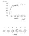
- FIG. 1illustrates qualitative behavior for the excess energy for crystalline, icosahedron and decahedron clusters
- FIG. 2illustrates a particle with a solid core and a surrounding liquid shell
- FIG. 3is a comparison of theoretical and experimental melting points for tin clusters
- FIG. 4illustrates growth simulation for copper nanoclusters
- FIG. 5illustrates graphs of absorption spectra calculated in the dipole approximation for prolate spheroidal Rh and Pt particles in water.
- the minor diameter of the particlesis 10 nm, and the aspect ratios are 1.0 ( - - - ), 2.0 ( - - - ), 3.0 ( - - - );
- FIG. 6illustrates polarization of a spherical metal particle by an electrical field vector of the incoming light
- FIG. 7illustrates absorption spectra of agglomerated (a) and isolated (b) particles of cadmium and thallium in water
- FIG. 8illustrates correlations between average particle size, powder color, ink color, and resistivity after photocuring
- FIG. 9illustrates absorption spectrum of an aged Cd solution before (O) and at various times after exposure to nitrous oxide
- FIG. 10illustrates evidence of reduction of copper oxide to metallic copper in a photo-curing process
- FIG. 11Aillustrates Sangyo copper nanoparticles ( ⁇ 50 nm) after pre-curing at 100° C. in air; Cu/Cu 2 O is 2.6:1 (28% Cu 2 O);
- FIG. 11Billustrates Sangyo nanoparticles after photo curing process (the intensity of the Cu 2 O peak is significantly reduced; Cu/Cu 20 is 13:1 (7% Cu 2 );
- FIG. 12Aillustrates American Elements copper nanoparticles pre-cured at 100° C. in air
- FIG. 12Cillustrates American Elements copper nanoparticles are photonic-cured at a voltage of 1400 V and reddish color is observed after photonic curing;
- FIG. 13illustrates a spectrum from a flash xenon lamp
- FIG. 14illustrates drying parameters in accordance with embodiments of the present invention
- FIG. 15illustrates that the electrical properties for samples 3-8 are very similar to that of sample 2;
- FIG. 16illustrates the percentage blowoff of the copper from the Kapton during a photosintering step
- FIG. 17illustrates drying parameters for each sample
- FIG. 18illustrates that the electrical properties for samples 5 and 7-10 are better than that of sample 2;
- FIG. 19illustrates the percentage blowoff of the copper from the Kapton during a photosintering step
- FIG. 20illustrates the drying parameters for each sample
- FIG. 21illustrates that samples 2-5 had increased resistivity when compared to that of sample 1;
- FIG. 22illustrates that samples 3 and 4 had low resistivity while having only 20% blowoff during photosintering
- FIG. 23illustrates electrical properties for the samples
- FIG. 24illustrates drying times
- FIG. 25illustrates percentage blowoff of copper from Kapton during a photosintering process
- FIGS. 26A and 26Billustrate a system and method for inkjetting and photo-curing of nanoparticle metal films.
- binding energy (E b ) of a cluster of size N with a given structurecan be written in the following form:
- volume contributionscorresponds to the volume contributions and the other represent surface contributions from facets, edges, and vertices (see, T. L. Hill, “Thermodynamics of Small Systems,” Parts I and II, 1964, Benjamin, Amsterdam). Volume and surface contributions are in competition. Clusters with low surface energy will have generally a quasi-spherical shape and close packed facets in order to optimize the surface to volume ratio.
- ⁇ ⁇ ( N )E b ⁇ ( N ) - N ⁇ ⁇ ⁇ coh N 2 / 3 ( 2 )
- ⁇ cohis the cohesive energy per particle in the bulk solid
- ⁇is the excess energy with respect to N atoms in a perfect bulk crystal.
- the size dependency of a nanocluster melting point for a given materialusually shows a monotonic decrease with decrease in size and may also show irregular variations.
- T m ⁇ ( N )T m ⁇ ( ⁇ ) ⁇ ⁇ 1 - C N 1 / 3 ⁇ ( 5 )
- Cis a constant and depends on the latent heat of melting per particle, the density of the particle, and interface tensions such as at the solid vapor interface and liquid vapor interface.
- This modelcan be refined by including the possibility of surface melting that may be the case in a photonic curing process. Id. In this case, the melting process is considered to start at the surface of a nanocluster as illustrated in FIG. 2 .
- FIG. 3shows a graph illustrating comparison of theoretical and experimental melting points of tin clusters (see, Lai, S. L., J. Y. Guo, V. Petrova, G. Ramanath, and L. H. Allen, 1996, Phys. Rev. Lett. 77, 99) showing clearly that this approach can theoretically predict the drop in the melting temperature of tin clusters versus size.
- the kinetic effectsmay strongly influence the formation of nanoclusters.
- An important considerationis the time scale of the copper nanocluster formation.
- the time scale of nanocluster formationmay range from a fraction of a millisecond to a few milliseconds.
- clustersmay not be able to reach the minimum free energy structure, thus remaining trapped in some meta-stable configuration that has a very long lifetime, especially when the clusters are further cooled down after their solidification, as is the case of the photo-curing process disclosed herein.
- this bathis more complicated, because it includes the substrate and the environment around the substrate.
- Another modelis referred to as a solid state growth model, and it is simulated by adding single atoms to a small initial seed at constant temperature. In photo-curing of copper nanoclusters, it may not be assumed that the temperature is constant, because there is an effect of freezing of liquid nano-droplets.
- a good modelis to mimic a thermal contact with the surroundings that is cooler. In such a way, one can take into account the most relevant parameters such as the rate of temperature change. Following this approach (see, Westergren, J., H. Gronbeck, A. Rosen, and S, Nordholm, 1998, J. Chem. Phys. 109, 9848), one can obtain that the change in the temperature is inversely proportional to the radius R of the nanocluster:
- FIG. 4illustrates the growth process of Cu 38 at a temperature of 400° K.
- the absorption coefficient in mol ⁇ 1 ⁇ L ⁇ cm ⁇ 1is calculated from the relation:
- the ratio R/ ⁇ Fis the mean time of the free movement of the electrons in the specific metal particle.
- FIG. 5shows, taking into account dipole approximation, a situation that explains well the absorption of metals below a wavelength of 400 nanometers.
- Creighton and Eadonsee, Creightoin, J. A., Eadon, D. G. J. Chem. Soc., Faraday Trans. 1991, 87, 3881
- FIG. 5shows, taking into account dipole approximation, a situation that explains well the absorption of metals below a wavelength of 400 nanometers.
- the electronic energy levels and the allowed optical transitions in the specific metalIn order to complete the entire picture of the absorption, one needs to take into account the electronic energy levels and the allowed optical transitions in the specific metal. First of all, one needs to treat the intraband transitions, which in some cases require the participation of a phonon.
- the movement of the electrons under the influence of the electric field vector of the incoming lightleads to a dipole excitation across the particle sphere.
- the positive polarization chargethen is acting as a restoring force which makes the electrons oscillate.
- the electron density within a surface layer of a few angstroms(which is about equal to the screening length) oscillates, while the interior of the particle remains constant.
- the excitation of the collective oscillations (plasmon absorption) and the intraband transitionsoccur at separated wavelength regimes.
- the plasmon resonancesoccur in the visible. However, these resonances are superimposed by intraband transitions.
- Copper nanoparticles( ⁇ 50 nm) from Sangyo and American Elements (80 nm) are formulated with B1-type ink (IPA, Hexylamie and copper nanoparticles). Both sets of copper nanoparticles contain copper oxides over 20%. Evidence shown in FIG. 10 indicates that photonic curing can photo-reduce copper oxides to metallic copper.
- FIG. 11( a )shows the Sangyo copper nanoparticles XRD after precuring at 100° C. in air; observed in FIG. 11( b ) are the changes to the XRD after the photonic curing process.
- the visual and XRD dataindicate that the reduction of copper oxide to metallic copper is occurring during photonic curing.
- the band gap of the metal oxideis greater than the enthalpy of formation of the metal oxide
- photo-reduction to metalcan be achieved by radiating the metal oxides having energy higher than the band gap.
- the band gaps for Cu 2 O and CuOare 1.9 eV (188 kJ/mol) and 2.6 eV (257 kJ/mol), respectively.
- the corresponding enthalpies of formation of Cu 2 O and CuOare 157 kJ/mol and 168 kJ/mol, respectively.
- the UV radiation from 100 nm to 400 nmreduces copper oxide to metallic copper.
- UV lamp containing decaying excimer complexesmay provide improved photonic curing lamps that can fuse and photo-reduce copper oxides at the same time.
- Excimer lampsoffer high intensity narrow band radiation at various UV and VUV wavelengths.
- Excimer lampscan be extremely efficient energy converters transforming electron kinetic energy into UV radiation. No self-absorption is observed in excimer systems. In most cases, excimer forming gas mixtures exhibit one dominant narrow emission band.
- Excimer systemscan be pumped at extremely high power densities before saturation effects start to limit the spontaneous emission. Thus, extremely bright UV and VUV sources can be built and used with embodiments of the present invention.
- a device 800is shown for simultaneous or near-simultaneous inkjetting and photo-curing of nanoparticle copper films (or any other suitable metal ink).
- the deviceincludes an inkjet dispenser 802 for dispensing copper ink 801 onto the surface of a substrate 804 .
- the device 800also includes a light source 806 for curing the ink films 803 deposited by the inkjet dispenser 802 .
- the light sourcecan be a laser source (pulsed or continuous), a pulsed lamp, or a focused beam.
- the dispenser 802is arranged to automatically pass over the substrate along a predetermined pathway.
- a thermal curing stepcan be introduced subsequent to dispensing the film and prior to the photo-curing step.
- the substrate and deposited filmcan be cured using an oven or by placing the substrate on the surface of a heater, such as a hot plate.
- the filmis pre-cured in air at 100° C. for 30 minutes before photo-curing.
- the thermal curingcan be performed by directing a laser onto the surface of the film.
- a laser beam or focused light from the light source 806is directed ( 816 ) onto the surface of the film in a process known as direct writing. The light serves to photo-cure the film such that it has low resistivity.
- the metal filmsare insulating after the printing/dispensing and drying steps. After the photo-curing process, however, the insulating film becomes a conductive film 809 (see FIG. 26A ).
- the dispenser 802is used to deposit a blanket film or a coarse outline of the pattern.
- printing techniquescan achieve feature sizes on the order of 25-50 microns or greater.
- the pattern/blanket filmcan be refined or reduced using a focused beam of light or laser, in which case the features are defined by the spot size of the laser or by the focus of the light beam.
- lightcan be focused to 1 micron or less.
- submicron featuresmay be possible.
- the feature sizemay be limited by the size of the nanoparticles used in the conductive film.
- Metal particlescan be formed to have features on the order of 1-5 nm.
- the formulated inkwas then sonicated and hand agitated to break up any agglomerations. It was used in a shelf life study for several weeks and then was stored on a shelf until this experiment. Prior to draw-down printing, the ink was hand agitated for approximately 30 seconds, sonicated for 16 minutes, and hand agitated for an additional 30 seconds.
- Printingwas accomplished using a draw-down printer on a Kapton substrate using a #10 wire-wrapped rod.
- the rodwas coated in ink and then drawn across the surface to provide an even coating.
- Several sampleswere printed in the same manner to accommodate the scope of the experiment. After printing, the samples were allowed to air dry on a shelf.
- FIG. 14shows the drying parameters for each sample. After heating and pumping the empty vacuum oven for outgassing and removing contaminants, the oven was then vented and the following procedure was used for each sample:
- Photosinteringis the previously described method used to cure the inks to a conductive copper film. This involves exposing the ink to a short pulse of highly concentrated UV light. All samples were photosintered using the same power and pulse widths for each shot. The power used was 1200 V and the pulse widths were 400, 500, 600, 700, and 800 microseconds.
- samples 3-8are very similar to that of sample 2, which was processed using a standard thermal procedure for this formulation.
- samples 9 and 10which were dried at 150° C. under vacuum significantly increased resistivity. Adhesion was excellent (10 on a scale of 1-10) for all samples in this experiment.
- FIG. 16shows the percentage blowoff of the copper from the Kapton during the photosintering step. These results show that resistivities in the micro-ohm-cm range with excellent adhesion are achieved in vacuum, and that comparable resistivities are obtained with vacuum drying for 5 minutes at 125° C. (sample #6) as compared to drying at 1 atmosphere pressure for 60 or 30 minutes at 100° C. Sample #6 has only 5% copper blowoff.
- the experimentwas performed using a commercially available infrared lamp to dry the samples at various distances to the lamp in open air. It was found that drying the sample at a short distance for any reasonable length of time as well as a medium distance for an extended length of time caused significant damage to the ink and in turn caused the ink to blow off during photosintering. Samples dried at medium to long distances for any length of time showed little change and, in some cases, slight improvement when compared with the sample dried in an airflow oven.
- this experimentcan also be expanded to include a greater variety of parameters (distance and time) to further enhance the viability of copper inks in a mass production setting.
- Solid copper nanoparticleswere added to the dispersion medium in an N 2 purged glove box, and the chunks were broken up in the media with a small spatula.
- the inkwas then sonicated and hand agitated to break up any agglomerations. It was used in a shelf-life study for several weeks and then was stored on a shelf. Just prior to draw-down printing, the ink was hand agitated for approximately 30 seconds, sonicated for 8 minutes, and hand agitated for an additional 30 seconds.
- Printingwas accomplished using a draw-down printer on a Kapton substrate using a #10 wire-wrapped rod. The rod was coated in ink and then drawn across the surface to provide an even coating. Several samples were printed in the same manner to accommodate the scope of the experiment. After printing, the samples were allowed to air dry on a shelf. One sample was left in this state before curing.
- FIG. 17shows the drying parameters for each sample.
- the sampleswere dried on an insulating ceramic platform to minimize heat transfer from the sample to the platform and vice-versa.
- FIG. 18the electrical properties for samples 5 and 7-10 are better than that of sample 2, which was processed using the standard bake for this formulation.
- samples 3 and 4which were dried at close range, infinite resistivity due to the film being completely blown off during the curing process.
- FIG. 19shows the percentage blowoff of the copper from the Kapton during the photosintering step.
- Sample #14had a low resistivity of 6.24 microohm-cm with a small blow off (30%) of the copper conductor (see FIGS. 18 and 19 ).
- the experimentwas performed for various periods of time, but at only one power level (100%). It was found that the drying time for the selected ink may not be reduced by microwave drying when compared to the baseline samples baked in an airflow oven. While the data collected from this experiment is believed to be sufficient in proving that drying times may be unaffected by microwave drying, this experiment may also be expanded to include different power levels and longer drying times to further enhance the data.
- Solid copper nanoparticleswere added to the dispersion medium in an N 2 purged glove box and chunks were broken up in the media with a small spatula.
- the inkwas then sonicated and hand agitated to break up any agglomerations. It was used in a shelf life study for several weeks and then was stored on a shelf until this experiment. Prior to draw-down printing, the ink was hand agitated for approximately 30 seconds, sonicated for 8 minutes and hand agitated for an additional 30 seconds.
- Printingwas accomplished using a draw-down printer on a Kapton substrate using a #10 wire-wrapped rod.
- the rodwas coated in ink and then drawn across the surface to provide an even coating.
- Several sampleswere printed in the same manner to accommodate the scope of the experiment. After printing, the samples were allowed to air dry on a shelf.
- FIG. 20shows the drying parameters for each sample. Each sample was placed in the center of the microwave on the rotating glass plate.
- FIG. 21shows that samples 2-5 had increased resistivity when compared to that of sample 1, which was processed using the standard bake for this formulation. Blowoff may be an issue with all samples ranging anywhere from 10% to 80% (see FIG. 22 ). Adhesion was marginal at best (3 to 8 on a 10 point scale) for all samples. This data indicates that microwave drying may not be a viable solution to shortening the drying time of copper nanoparticle inks.
- the inkwas a water-based copper ink.
- the data in FIG. 23shows the electrical properties for the samples in FIG. 24 .
- the post-sintering thickness for sample 1is in question, hence the unrealistically low resistivity.
- FIG. 25shows the percentage blowoff of the copper from the Kapton during the photosintering step.
- optical absorption of copper inksis a complicated system of many particles, which is determined by both properties of the individual structural units and the collective effects due to the interaction among particles.
- This spectrumoften contains both the plasmon band of the single particles and sometimes more maxima attributed to excitation with the electric field parallel (low energy mode) and normal (high energy mode) to the axes of a chain of agglomerated particles.
- approximation of the metallic particle to a spherical shapeis not accurate anymore, and one needs to look at a prolate spheroidal as the calculations were made in FIG. 5 .
- FIG. 5observed from FIG. 5 is that as the agglomerates become more ellipsoid-like, the spectrum is changing from Spectra (b) to Spectra (a), as discussed above.
Landscapes
- Engineering & Computer Science (AREA)
- Manufacturing & Machinery (AREA)
- Microelectronics & Electronic Packaging (AREA)
- Chemical & Material Sciences (AREA)
- Powder Metallurgy (AREA)
- Manufacture Of Metal Powder And Suspensions Thereof (AREA)
- Life Sciences & Earth Sciences (AREA)
- Materials Engineering (AREA)
- Wood Science & Technology (AREA)
- Organic Chemistry (AREA)
- Inks, Pencil-Leads, Or Crayons (AREA)
- Manufacturing Of Printed Wiring (AREA)
- Conductive Materials (AREA)
- Manufacturing Of Electric Cables (AREA)
Abstract
Description
- This application claims priority to U.S. Provisional Patent Application Ser. Nos. 61/053,574 and 61/169,618, which are hereby incorporated by reference herein.
- The present invention relates in general to metallic inks for producing conductive paths for electronic circuitry.
- The purpose of nanotechnology and science is to understand, control and manipulate objects of a few nanometers in size. These nano-objects are known to behave as an intermediate between single atoms and molecules and bulk matter. These properties are often peculiar and different from the properties of bulk material; in particular, these nano-objects can present properties that vary dramatically with size. This opens the possibility of controlling these properties by precisely controlling their formulation process.
- Nanoclusters are aggregates of atoms or molecules with an average diameter less than 100 nm and a number of constituent components ranging from 10 to 106. Nanoclusters do not have a fixed size, structure, or composition. As a result, they present a variety of morphologies. Nanoclusters may be homogeneous, which means composed of only one type of atom or molecule, or heterogeneous. The components within a nanocluster may be held together by very different kinds of forces, such as electro-static, Van der Waals, or covalent bonds, depending on the constituent. Small clusters of metal atoms, such as Cu (copper), are held together by forces more like those of covalent bonds, not like the forces exerted by the nearly free electrons of bulk metals. Clusters containing no more than a few hundred metal atoms, resulting in diameters around 3-5 nanometers, have strong, size-dependent properties due to quantum confinement. As the cluster becomes larger, with diameters up to 100 nanometers, they possess smooth variations of behavior approaching the bulk size limit.
- Nanoclusters usually do not have a crystal lattice structure like their bulk counterparts. These finite clusters can present multiple nanocrystalline structures such as multiple hedronic structures with multiple faces. Some nanoclusters may be a crystalline solid. It is important to understand whether crystalline or noncrystalline structures prevail for a given size and composition in order to describe some physical process involving the nanocluster.
- An interesting inquiry for consideration is what happens in a phase transition situation, like copper from liquid to solid, when there are nanoclusters. An answer to this question provides that thermodynamic and kinetic energy stabilities influence. Nanoclusters have a very high surface area to volume ratio resulting in a high surface energy. The nanocluster's structure, including facets, edges and vertices, has a strong influence to this surface energy and thus dominates the nanoparticle's behavior.
- In order to fully understand the physical behavior of these nanoclusters several steps are taken. First, nanoparticle structure is the starting point for understanding copper nanocluster behavior. In order to gain a very complicated understanding of the structure-property relationship, a deep study of the minimum energetic situations was performed and the results analyzed. These results are very complicated and convoluted and, until now, has not been done by anyone in the world for copper nanoclusters. Second, is to determine the effect of increased temperature. To answer this question, one must be an expert in the thermodynamics of finite systems. There are very few experts in the world. Third, one needs to understand, in particular for phase transition of copper nanoclusters, what is the time scale in the experimental setting vs. the time scale of morphology transitions. Basically, this is solved by the study of kinetic effects in the formation and destruction of nanoclusters.
FIG. 1 illustrates qualitative behavior for the excess energy for crystalline, icosahedron and decahedron clusters;FIG. 2 illustrates a particle with a solid core and a surrounding liquid shell;FIG. 3 is a comparison of theoretical and experimental melting points for tin clusters;FIG. 4 illustrates growth simulation for copper nanoclusters;FIG. 5 illustrates graphs of absorption spectra calculated in the dipole approximation for prolate spheroidal Rh and Pt particles in water. The minor diameter of the particles is 10 nm, and the aspect ratios are 1.0 ( - - - ), 2.0 ( - - - ), 3.0 ( - - - );FIG. 6 illustrates polarization of a spherical metal particle by an electrical field vector of the incoming light;FIG. 7 illustrates absorption spectra of agglomerated (a) and isolated (b) particles of cadmium and thallium in water;FIG. 8 illustrates correlations between average particle size, powder color, ink color, and resistivity after photocuring;FIG. 9 illustrates absorption spectrum of an aged Cd solution before (O) and at various times after exposure to nitrous oxide;FIG. 10 illustrates evidence of reduction of copper oxide to metallic copper in a photo-curing process;FIG. 11A illustrates Sangyo copper nanoparticles (˜50 nm) after pre-curing at 100° C. in air; Cu/Cu2O is 2.6:1 (28% Cu2O);FIG. 11B illustrates Sangyo nanoparticles after photo curing process (the intensity of the Cu2O peak is significantly reduced; Cu/Cu20is 13:1 (7% Cu2);FIG. 12A illustrates American Elements copper nanoparticles pre-cured at 100° C. in air;FIG. 12B illustrates American Elements copper nanoparticles are photonic-cured at a voltage of 1300 V and bluish color is observed after photonic curing;FIG. 12C illustrates American Elements copper nanoparticles are photonic-cured at a voltage of 1400 V and reddish color is observed after photonic curing;FIG. 13 illustrates a spectrum from a flash xenon lamp;FIG. 14 illustrates drying parameters in accordance with embodiments of the present invention;FIG. 15 illustrates that the electrical properties for samples 3-8 are very similar to that ofsample 2;FIG. 16 illustrates the percentage blowoff of the copper from the Kapton during a photosintering step;FIG. 17 illustrates drying parameters for each sample;FIG. 18 illustrates that the electrical properties forsamples 5 and 7-10 are better than that ofsample 2;FIG. 19 illustrates the percentage blowoff of the copper from the Kapton during a photosintering step;FIG. 20 illustrates the drying parameters for each sample;FIG. 21 illustrates that samples 2-5 had increased resistivity when compared to that ofsample 1;FIG. 22 illustrates thatsamples FIG. 23 illustrates electrical properties for the samples;FIG. 24 illustrates drying times;FIG. 25 illustrates percentage blowoff of copper from Kapton during a photosintering process; andFIGS. 26A and 26B illustrate a system and method for inkjetting and photo-curing of nanoparticle metal films.- In general, the binding energy (Eb) of a cluster of size N with a given structure can be written in the following form:
Eb=aN+bN2/3+cN1/3+d (1)- where the first term corresponds to the volume contributions and the other represent surface contributions from facets, edges, and vertices (see, T. L. Hill, “Thermodynamics of Small Systems,” Parts I and II, 1964, Benjamin, Amsterdam). Volume and surface contributions are in competition. Clusters with low surface energy will have generally a quasi-spherical shape and close packed facets in order to optimize the surface to volume ratio.
- From equation (1), one can define a useful parameter that reflects the stability of the cluster with the size N:
- whereby εcohis the cohesive energy per particle in the bulk solid, and Δ is the excess energy with respect to N atoms in a perfect bulk crystal. For clusters of crystalline structure, the parameter a in equation (1) is simply εcohso that:
lim Δ=Eb
N→∞ (3)- As illustrated in the graph in
FIG. 1 , in the case of nanocrystalline structures, α>εcoh, and Δ diverges as large sizes. - It is important to understand, empirically and theoretically, what are the different cluster shapes that a solid copper nanocluster can take in order to exactly emulate and calculate the phase transitions from solid to liquid and from liquid to solid in the fusion process that takes place utilizing photonic curing.
- The literature provides solutions for building up different shapes with the lowest energy possible (see, A. L. Mackay, 1962, Acta Crystallogr. 15, 916; Martin, T. P., 1996, Phys. Rep. 273, 199), such as icosahedra (twenty facets) and decahedra (ten facets).
- With respect to copper clusters specifically, some work was done (see, Alonso, J. A., 2000, Chem. Rev. (Washington, D.C.) 100, 637) to understand the energetic properties of small copper nanoclusters. For example, it was found that for N<10, there is evidence of possibilities for planar structures (flakes) for small N; as the N grows to around 1015, the icosahedra is favored over the cubical hedron. To understand the energetics of these clusters, very complicated calculations and studies based on density functional calculations (see, Jug, K., B. Zummerman, and A. M. Kostler, 2002, Int. J. Quantum Chem. 90. 594) or semi-empirical potential calculations (see, Darby, S., T. V. Mortimer-Jones, R. L. Johnson, and C. Roberts, 2002, J. Chem. Phys. 116, 1536; Doye, J. P., and D. J. Wales, 1998b, New J. Chem. 22, 733) must be performed. In any case, all these calculations compared with some few experimental results show for nanoclusters of copper a prevalence for icosahedra, intermediate sized decahedra, and large face cubic center (fcc) clusters.
- An important point is to understand the size dependence of the melting point. The size dependency of a nanocluster melting point for a given material usually shows a monotonic decrease with decrease in size and may also show irregular variations.
- Consider a cluster of size N and, for simplicity, of spherical shape, at a given pressure p. It is expected then that the melting temperature will be a function of the size Tm(N). Comparison of Tm(N) with Tm(∞) is then performed, which is the melting temperature of the bulk material. In the case of photo-curing of copper nanoclusters, it is important to study the solid-liquid transitions of these nanoclusters. In order to find a solution to Tm(N), one needs to equate the chemical potential of the solid and of the liquid and solve the equation:
μs(p,T)=μl(p,T) (4)- This equation means that the chemical potentials of a fully solid and of a fully liquid cluster are equal at melting. After a number of mathematical manipulations (see, Pawlow, P., 1909, Z. Phys. Chem., Stoechiom. Verwandtschaftsl. 65, 1), one obtains the following equation:
- where C is a constant and depends on the latent heat of melting per particle, the density of the particle, and interface tensions such as at the solid vapor interface and liquid vapor interface.
- This model can be refined by including the possibility of surface melting that may be the case in a photonic curing process. Id. In this case, the melting process is considered to start at the surface of a nanocluster as illustrated in
FIG. 2 . - The melting temperature is found by imposing the equilibrium condition on the solid core/liquid shell particle. This model is even further complicated and expanded (see, Kofman, R., P. Cheyssac, A. Aouaj, Y. Lereah, G. Deutscher, T. Ben-David, J. M. Pennison, and A. Bourret, 1994, Surf. Sci. 303, 231) for metallic particles, specifically. In this case, a new variable ξ is introduced that is characteristic to the length of the interaction among atoms and liquid metals in addition to taking into account the effective interaction between the solid liquid and liquid vapor interfaces. This effective interaction is repulsive and favors the formation of a liquid shell between the solid core and the vapor as illustrated in
FIG. 2 . The equation is much more complex, but it is interesting to see that the simple solution expressed in equation (5) is recovered in thelimit ξ→ 0. - It is believed that the solid core/liquid shell model is more accurate and fits the experiment much better. In fact, some researchers (Wang, L., Y. Zhang, X. Bian, and Y. Chen, 2003, Phys. Lett. A 310, 197) discovered that this solid core/liquid shell model fits very well for N=500 for copper. For example,
FIG. 3 shows a graph illustrating comparison of theoretical and experimental melting points of tin clusters (see, Lai, S. L., J. Y. Guo, V. Petrova, G. Ramanath, and L. H. Allen, 1996, Phys. Rev. Lett. 77, 99) showing clearly that this approach can theoretically predict the drop in the melting temperature of tin clusters versus size. - For the photonic curing process, consider both the melting process of the copper nanoclusters and the formation of the copper nanoclusters in a process of freezing the liquid copper nano-droplets. In particular, the kinetic effects may strongly influence the formation of nanoclusters. An important consideration is the time scale of the copper nanocluster formation. The time scale of nanocluster formation may range from a fraction of a millisecond to a few milliseconds. On this time scale, from the kinetics point of view, clusters may not be able to reach the minimum free energy structure, thus remaining trapped in some meta-stable configuration that has a very long lifetime, especially when the clusters are further cooled down after their solidification, as is the case of the photo-curing process disclosed herein.
- In order to build a model and study the formation process of solid clusters of copper in the herein described photo-curing process, solid clusters in contact with a thermal bath are studied. In an embodiment of the present invention, this bath is more complicated, because it includes the substrate and the environment around the substrate.
- There are two models for studying the formation of nanoclusters. One is referred to as a liquid state growth model, and is simulated by freezing a liquid droplet until it solidifies, usually at constant N and decreasing T. In the case of copper metal, it is not necessary to take care in this type of calculations of the evaporation of atoms effects, because there are very large differences between melting and boiling points; as a result, the evaporative cooling is negligible.
- Another model is referred to as a solid state growth model, and it is simulated by adding single atoms to a small initial seed at constant temperature. In photo-curing of copper nanoclusters, it may not be assumed that the temperature is constant, because there is an effect of freezing of liquid nano-droplets.
- A good model is to mimic a thermal contact with the surroundings that is cooler. In such a way, one can take into account the most relevant parameters such as the rate of temperature change. Following this approach (see, Westergren, J., H. Gronbeck, A. Rosen, and S, Nordholm, 1998, J. Chem. Phys. 109, 9848), one can obtain that the change in the temperature is inversely proportional to the radius R of the nanocluster:
- The growth of copper nanoclusters is dominated by polyicosahedral structures, as mentioned above. It is interesting to note that theoretically it was proven that there are some magic sizes, or values of N, that these polyicosahedral structures prefer, meaning they have the most stability. For example,
FIG. 4 illustrates the growth process of Cu38at a temperature of 400° K. - To understand the photo-curing process, one takes into account the anomalous heat capacity of nanoparticles (see, Likhachev, V. N, et al, Anomalous heat capacity of nanoparticles, Phys. Lett. A 357, 236). The question is why one should expect at all an anomalous heat capacity behavior of nanoclusters or nanoparticles. Under most circumstances, such a heat capacity is qualitatively similar to that of the bulk counterpart. The problem is, however, that in the formation of the nanoclusters or their melting, there is a region of coexistence of two or more phases. This issue can create some peculiar behavior of heat capacity. In the photo-curing process, there is a situation of phase changes of nanoclusters. The thermodynamics of such small systems is outside the range of the regular textbook of thermodynamics.
- Refer to the equilibrium for two phases for understanding. The equilibrium between two phases, whether in a bulk form or nanocluster form, can be described by an equilibrium constant:
Keq(T)=exp(−ΔAF/KT) (7)- whereby ΔF is the free energy difference between the solid and the liquid. However, it is known that:
ΔF=NΔμ (8)- And as a result, the equilibrium constant can be expressed as:
Keq(T)=exp(−NΔμ/KT) (9)- where N is the number of particles in the system, and Δμ is the mean difference in the chemical potentials of the two phases.
- Hence, even if Δμ/KT is very small (approximately 10−10), but N is of order of 1020, then the thermodynamically unfavored phase is so unfavored that it is simply unobservable. However, if N is of order of 10 or 1000, then as long as each phase persists long enough to establish conventional properties by which it is recognized as such, it can be quite easy to find ranges of temperatures and pressure in which two or more phases may coexist in thermodynamic equilibrium. Indeed, as discussed above, in the case of copper nanocluster melting or freezing, there may be situations where isomers may coexist, which as a result may induce the anomalous heat capacity behavior. This is taken into account, as well as other variables, when modeling the photonic curing as temperature induced phase transitions in copper nanoclusters. This type of modeling uses extensive molecular dynamics (MD) and jump-walking Monte Carlo (MC) simulations (see, Proykova, A., et al., “Temperature induced phase transformations of molecular nanoclusters,” Vacuum, 68 (2003), 87), which needs to treat solid-solid transformation, solid-liquid transformation, and cooling below the solidification point phenomena. This is very complex and uses several millions of configurations and averaging these simulations over different clusters with the same size. This type of calculation and modeling is out of the scope of the photonic curing experimentations.
- The complication of the modeling is even more extensive if one takes into account coalescence. The process is so complex that one must consider the coalescence between two solid clusters, a liquid and a solid cluster and two liquid clusters; while the coalescence of two liquid clusters takes place rapidly, the process of coalescence of two solid clusters takes much longer.
- In any case, researchers concluded that coalescence of two solid clusters is very complex, takes place on a very slow time scale and may involve either the formation of a single domain cluster or complicated structures presenting grains (see, Zhu, H., 1996, Philos. Mag. Lett. 73, 27). What exactly happens depends on size and structure of the initial clusters, so it may be a function in photo-curing of the initial size of copper nanoparticles that are used.
- The photo-curing process, involves a study and analyzation of the light absorption by small metal particles. The theory of light absorption by small particles is described by Mie's formulation (see, Mie, G., Ann. Phys. 1908, 25, 377). The absorption spectrum of particles in a given solvent can be calculated from the optical constants of the bulk metal, although the absorption of the particles is recognized to be often vastly different from that of the bulk metal itself. The simplest case is when the particles are spherical and their size is small compared to the wavelength of light. Furthermore, to simplify, assume that the particles are well separated in the solution. Following Mie's theory, at particle sizes between about 3 and 20 nanometers, there is no strong dependence of the absorption spectra on particle size. This is because at this very small particle size, the mean free path of the electrons of the bulk metals is much larger, and as a result, the most significant term in Mie's formula is due to the dipole term, which depends only on the total metal concentration in the solution, not the particle size. In this case, the absorption coefficient in mol−1·L·cm−1is calculated from the relation:
- where:
- λ is the wavelength of light in nm;
- M is the molecular weight;
- ρ is the density of the metal;
- n0is the refractive index of the solvent; and
- ε1, ε2are the real and the imaginary parts of the dielectric constant of the metal.
- An interesting situation is when the size of the particles becomes smaller than the mean free path of the electrons (for silver, 52 nanometers, and for copper, 39 nanometers). In this case, the absorption bands are broadened. The reason is that a size correction is necessary, and the formula equation (10) starts to be size-dependant (see Kreibig, U., J. Phys.
F 1974, 4, 999), because
ε2=ε2(bulk)+(ωp2/ω3)(νF/R) (11)- where:
- ω is the light frequency;
- ωpis the plasmon frequency of the specific metal;
- νFis the electron velocity at the Fermi level; and
- R is the particle radius.
- Basically, the ratio R/νFis the mean time of the free movement of the electrons in the specific metal particle.
- Extensive modeling and calculations using Mie's formulation were done by Creighton and Eadon (see, Creightoin, J. A., Eadon, D. G. J. Chem. Soc., Faraday Trans. 1991, 87, 3881) (see
FIG. 5 ).FIG. 5 shows, taking into account dipole approximation, a situation that explains well the absorption of metals below a wavelength of 400 nanometers. In order to complete the entire picture of the absorption, one needs to take into account the electronic energy levels and the allowed optical transitions in the specific metal. First of all, one needs to treat the intraband transitions, which in some cases require the participation of a phonon. If this is the case, these intraband transitions will not significantly contribute to the absorption of light. However, an intense absorption is observed in some metallic particles, which peaks at a lower photon energy that is produced by a collective excitation of the free electrons in the particles, as it is illustrated inFIG. 6 . - Referring to
FIG. 6 , the movement of the electrons under the influence of the electric field vector of the incoming light leads to a dipole excitation across the particle sphere. The positive polarization charge then is acting as a restoring force which makes the electrons oscillate. Thus, the electron density within a surface layer of a few angstroms (which is about equal to the screening length) oscillates, while the interior of the particle remains constant. It is important to note that in some cases (such as silver), the excitation of the collective oscillations (plasmon absorption) and the intraband transitions occur at separated wavelength regimes. In the case of copper (as well as gold), the plasmon resonances occur in the visible. However, these resonances are superimposed by intraband transitions. - The contribution of the plasmon oscillation to the absorption of a metal particle can be treated separately. For example, the Mie's equation for the absorption constant is then described as:
K=9πNVn03cλ2/σ[(λm2−λ2)2+λ2λm2/λa2] (12)- where
- K is the absorption constant in cm−1, K=αc ln 10, whereby c is the concentration of the metal in moles/liter;
- N is the particle concentration;
- V is the volume per particle;
- λm2=λc2(ε0+2n02) is the wavelength of maximum absorption;
- ε0is the high frequency dielectric constant of the metal;
- λcis the plasma wavelength, λc2=(2πc)2 m/4πNee2, and is a typical metal property;
- Neis the density of the free electrons;
- λais constant related to the bandwidth at half maximum absorption, λm2/λa=(ε0+2n02)c/2σ;
- σ is the DC conductivity, σ=Nee2{r}/mνF;
- M is the effective electron mass;
- {r} is mean free path of the electrons in the colloid;
- 1/{r}=(1/r+1/r∞); and
- r∞ is the mean free path in the bulk metal.
- The relations above indicate that the band position does not depend on the size of the particles. An increase in Neby adding electrons to the particles' surfaces should lead to a blue shift and a decrease in bandwidth, and consequently, to an increase in the absorption maximum.
- A good comparison between experiment and calculations of observed spectra has been previously possible for a limited number of cases. The main reason is that the metal often does not form isolated particles in colloidal solutions, but agglomerates of a few or even a large number of particles. The agglomeration can drastically change the absorption spectrum. Typical examples are shown in
FIG. 7 where absorption spectrums of cadmium and thallium colloids are graphed. - Spectra (a) in
FIG. 7 were obtained for solutions which contain agglomerated particles, while Spectra (b) were obtained for solutions prepared under conditions where agglomeration did not occur. Spectra (b) is in good agreement with Mie's formulation and also with the calculated spectrum inFIG. 5 . - In view of the description above and the results in
FIG. 7 , a colloidal metallic substance appears black if the spectrum is similar to the Spectra (a). On the other hand, if the particles are not agglomerated (i.e., good dispersion and good isolation between particles), observed is a more metallic-like color, indicated by Spectra (b). - As summarized in
FIG. 8 , there is a resulting correlation between average particle size, the powder color, the ink color and the resistivity after curing. Good inks are produced when the color of the powder and the inks are in the red-brown or brown range. When there are very black or very dark looking particles and inks, there is agglomeration. - As the solution is aging, there is a dynamic change of the absorption spectrum from Spectra (b) to Spectra (a) (see
FIG. 7 ). The reason is that at the initial stage there are well-dispersed and isolated copper nanoparticles, while due to the aging process, there will be larger and larger agglomerations. As a result, the color of the copper colloid changes from a metallic red-brownish color to a darker color, eventually transitioning to black. - A very interesting experiment is described (see, Henglein, A., J. Phys. Chem. 1993, 97, 5457-5471) in the spectrum of an aged cadmium (Cd) solution. The aged cadmium solution was exposed to nitrous oxide and then the spectrum was measured as a function of time. The cadmium particles slowly react with N2O according to the following equation:
Cd0+N2O+H2O→(Cd+++N2+2OH− (13)- As can be seen in
FIG. 9 , not only the intensity of the absorption decreases during this reaction, but also the shape of the spectrum, with the long wavelength peak rapidly disappearing. The effect is attributed to a phenomenon that occurs frequently in redox reactions of agglomerated colloids color; the agglomerates disintegrated to yield more or less isolated particles. This is attributed to charging of the particles: as the reaction with N2O is progressing, the particles become positively charged and repel each other. - Copper nanoparticles (˜50 nm) from Sangyo and American Elements (80 nm) are formulated with B1-type ink (IPA, Hexylamie and copper nanoparticles). Both sets of copper nanoparticles contain copper oxides over 20%. Evidence shown in
FIG. 10 indicates that photonic curing can photo-reduce copper oxides to metallic copper. - With a flash lamp, a threshold energy may exist for photo-reduction of copper oxides. Respective XRDs of the photo-cured inks were executed for both Sangyo and American Elements B1 type ink formulations.
FIG. 11( a) shows the Sangyo copper nanoparticles XRD after precuring at 100° C. in air; observed inFIG. 11( b) are the changes to the XRD after the photonic curing process. - In this case, Cu2O was completely transformed to copper (200). The same phenomena was observed with American Elements copper nanoparticles, but in this case dependency on the voltage of the photo-curing lamp was observed (see
FIG. 12 ).FIG. 12A illustrates American Elements copper nanoparticles pre-cured at 100° C. in air;FIG. 12B illustrates American Elements copper nanoparticles are photonic-cured at a voltage of 1300 V and bluish color is observed after photonic curing;FIG. 12C illustrates American Elements copper nanoparticles are photonic-cured at a voltage of 1400 V and reddish color is observed after photonic curing. - The visual and XRD data indicate that the reduction of copper oxide to metallic copper is occurring during photonic curing. Following the work of Fleisch (T. H. Fleisch, et al., J. App. Surf. Sci., 10, 50 (1982)), when the band gap of the metal oxide is greater than the enthalpy of formation of the metal oxide, photo-reduction to metal can be achieved by radiating the metal oxides having energy higher than the band gap. The band gaps for Cu2O and CuO are 1.9 eV (188 kJ/mol) and 2.6 eV (257 kJ/mol), respectively. The corresponding enthalpies of formation of Cu2O and CuO are 157 kJ/mol and 168 kJ/mol, respectively. Thus, the UV radiation from 100 nm to 400 nm reduces copper oxide to metallic copper.
- Based on the analysis of the optical absorption spectrum, the spectral distribution of the flash lamp is important. The spectral distribution illustrated in
FIG. 13 is typical of a xenon lamp whereby approximately 6% of the power used is emitted in the form of UV radiation below 380 nm. Most of the photonic energy actually ranges from visible to infrared wavelengths. It may be useful to have the UV lamp with a higher energy density in UV range as compared with the current flash lamp. - Another possible UV lamp containing decaying excimer complexes may provide improved photonic curing lamps that can fuse and photo-reduce copper oxides at the same time. Excimer lamps offer high intensity narrow band radiation at various UV and VUV wavelengths. Excimer lamps can be extremely efficient energy converters transforming electron kinetic energy into UV radiation. No self-absorption is observed in excimer systems. In most cases, excimer forming gas mixtures exhibit one dominant narrow emission band. Excimer systems can be pumped at extremely high power densities before saturation effects start to limit the spontaneous emission. Thus, extremely bright UV and VUV sources can be built and used with embodiments of the present invention.
- This analysis also explains results with the Optomec printer, and may direct even further to a better choice or laser mono-chromatic radiation for achieving the best curing results.
- As noted previously, in a process to photosinter metallic inks, they are pre-dried to remove excess vehicles and solvents. This can be carried out in air including with the aid of an oven, but this may require 30-60 minutes of drying time. In a manufacturing process, this time may be too long. The following alternative embodiment describes methods of reducing this drying time.
- Referring to
FIG. 26A , adevice 800 is shown for simultaneous or near-simultaneous inkjetting and photo-curing of nanoparticle copper films (or any other suitable metal ink). The device includes aninkjet dispenser 802 for dispensingcopper ink 801 onto the surface of asubstrate 804. Thedevice 800 also includes alight source 806 for curing theink films 803 deposited by theinkjet dispenser 802. The light source can be a laser source (pulsed or continuous), a pulsed lamp, or a focused beam. In some implementations, thedispenser 802 is arranged to automatically pass over the substrate along a predetermined pathway. Additionally, thedispenser 802 can be arranged to dispense the copper ink at multiple predetermined positions and times above thesubstrate 804. Thelight source 806 can be attached to theinkjet dispenser 802 or arranged to travel over thesubstrate 800 separately from thedispenser 802. Thelight source 806 can be arranged to photo-cure the inkjetted films immediately after they are deposited by thedispenser 802. Alternatively, thelight source 806 can be arranged to photo-cure the films at predetermined times following the deposition of the film. The motion of thelight source 806 and thedispenser 802 can be controlled by a computer system/controller arrangement 808. A user may program thecomputer 808 such that the controller automatically translates thedispenser 802 andlight source 806 over a predetermined path. In some implementations, thelight source 806 anddispenser 802 are fixed and the substrate is placed on a movable platform controlled by the computer/controller 808. - A flow chart of a photo-curing process is shown in
FIG. 26B . A solution of metal ink is mixed (810) and then printed or dispensed (812) onto thesubstrate 804 using thedispenser 802. The film deposition is tightly controlled so a well-defined pattern is formed. The film then is dried (814 ) to eliminate water or solvents. - In some cases, a thermal curing step can be introduced subsequent to dispensing the film and prior to the photo-curing step. The substrate and deposited film can be cured using an oven or by placing the substrate on the surface of a heater, such as a hot plate. For example, in some implementations, the film is pre-cured in air at 100° C. for 30 minutes before photo-curing. Alternatively, the thermal curing can be performed by directing a laser onto the surface of the film. Following the drying and/or thermal curing step, a laser beam or focused light from the
light source 806 is directed (816) onto the surface of the film in a process known as direct writing. The light serves to photo-cure the film such that it has low resistivity. Generally, the metal films are insulating after the printing/dispensing and drying steps. After the photo-curing process, however, the insulating film becomes a conductive film809 (seeFIG. 26A ). - In some implementations, the
dispenser 802 is used to deposit a blanket film or a coarse outline of the pattern. Typically, printing techniques can achieve feature sizes on the order of 25-50 microns or greater. If finer features are necessary, the pattern/blanket film can be refined or reduced using a focused beam of light or laser, in which case the features are defined by the spot size of the laser or by the focus of the light beam. Typically, light can be focused to 1 micron or less. Thus, submicron features may be possible. Ultimately, the feature size may be limited by the size of the nanoparticles used in the conductive film. Metal particles can be formed to have features on the order of 1-5 nm. - An experiment was performed to determine the effect of drying the copper nanoparticle inks in a vacuum environment as opposed to an airflow environment. The sample was prepared by sonication and hand agitation. The samples were then printed and dried. Then a vacuum oven was used to dry the inks at various temperatures. For comparison, baseline samples were also prepared in an airflow environment at atmosphere. All samples were photosintered, and the electrical and adhesive properties were measured. A result is that the drying time for the selected ink is significantly reduced if the drying takes place in a vacuum environment.
- Processes above describe copper ink samples dried in an airflow environment at atmospheric pressure for 30-60 minutes, depending upon the formulation of the ink. This drying is performed in order to remove by evaporation the solvents that remain in the ink after printing. Evaporation of the solvents aids in the photosintering process that follows. If the ink contains excessive amounts of solvent, the result is what is referred to as “blowoff,” a condition where the solvent evaporates rapidly, in fact almost instantly, causing the copper nanoparticles to be blasted off of the substrate and into the surrounding environment.
- By removing the solvents more rapidly, the process can be more cost effective for a high-throughput manufacturing system. Experiments were performed at various temperatures but at one vacuum level. It was found that the drying time for a selected ink is reduced when dried at 100° C. or 125° C. without significantly affecting the conductive or adhesive properties when compared to the baseline samples dried in an airflow environment. At 150° C., however, the conductive properties tend to diminish. While the data collected from this experiment proves that drying times are shortened through vacuum drying, this process may also be expanded to include lower temperatures and shorter drying times to further enhance the viability of copper inks in a mass production scenario.
- The formulated ink was then sonicated and hand agitated to break up any agglomerations. It was used in a shelf life study for several weeks and then was stored on a shelf until this experiment. Prior to draw-down printing, the ink was hand agitated for approximately 30 seconds, sonicated for 16 minutes, and hand agitated for an additional 30 seconds.
- Draw-Down Printing
- Printing was accomplished using a draw-down printer on a Kapton substrate using a #10 wire-wrapped rod. The rod was coated in ink and then drawn across the surface to provide an even coating. Several samples were printed in the same manner to accommodate the scope of the experiment. After printing, the samples were allowed to air dry on a shelf.
- Airflow Drying
- Two samples were dried in an airflow oven at 100° C., one for 30 minutes and one for 60 minutes. These samples were made to provide a baseline of a standard procedure for later comparison to the vacuum dried samples.
- Vacuum Drying
- The remaining samples were dried in a vacuum oven at various temperatures and for various lengths of time.
FIG. 14 shows the drying parameters for each sample. After heating and pumping the empty vacuum oven for outgassing and removing contaminants, the oven was then vented and the following procedure was used for each sample: - Check and record platform temperature by an infrared (IR) thermometer
- Place the sample in the center of the platform
- Begin vacuum pumping
- When pressure reaches approximately −25 inches Hg (93 seconds on average), start the timer
- When time has expired, record oven pressure (approximately −29.5 inches Hg for all samples)
- Immediately vent the oven
- When the oven is vented, check and record platform temperature with the IR thermometer
- Repeat for all samples
- Presintering Preparation
- Upon completion of the airflow and vacuum drying, all samples were then scored to provide an adhesion test pattern. The samples were also numbered and measured on a profilometer to provide thickness data before the photosintering step.
- Photosintering
- Photosintering is the previously described method used to cure the inks to a conductive copper film. This involves exposing the ink to a short pulse of highly concentrated UV light. All samples were photosintered using the same power and pulse widths for each shot. The power used was 1200 V and the pulse widths were 400, 500, 600, 700, and 800 microseconds.
- Properties Testing
- After photosintering was complete, the adhesive and electrical properties of each sample were characterized. First, sheet resistance of the film was measured using a 4-point probe method. Second, the film thickness was measured on the profilometer. Finally, the adhesion was tested using the ASTM Standard Test Method for Measuring Adhesion by Tape Test. After all data were collected, the resistivity was calculated using the sheet resistance and thickness data.
- Results
- Referring to
FIG. 15 , the electrical properties for samples 3-8 are very similar to that ofsample 2, which was processed using a standard thermal procedure for this formulation. However,samples FIG. 16 shows the percentage blowoff of the copper from the Kapton during the photosintering step. These results show that resistivities in the micro-ohm-cm range with excellent adhesion are achieved in vacuum, and that comparable resistivities are obtained with vacuum drying for 5 minutes at 125° C. (sample #6) as compared to drying at 1 atmosphere pressure for 60 or 30 minutes at 100°C. Sample # 6 has only 5% copper blowoff. - An experiment was performed to determine the effect of drying copper nanoparticle inks under an infrared lamp as opposed to an airflow oven environment (standard drying process). The sample was prepared by sonication and hand agitation. The samples were then printed and air dried. An infrared lamp was then used at various distances to further dry the inks. For comparison, one sample was cured with no drying process and another sample was dried in an airflow oven environment. All samples were photosintered, and electrical and adhesive properties were measured. The data collected in this experiment indicates that drying by infrared lamp reduces the drying time required when compared to airflow oven drying. Interestingly, the sample that was not subjected to any drying process showed similar electrical properties to the sample that was dried in an airflow oven.
- The experiment was performed using a commercially available infrared lamp to dry the samples at various distances to the lamp in open air. It was found that drying the sample at a short distance for any reasonable length of time as well as a medium distance for an extended length of time caused significant damage to the ink and in turn caused the ink to blow off during photosintering. Samples dried at medium to long distances for any length of time showed little change and, in some cases, slight improvement when compared with the sample dried in an airflow oven.
- While the data collected from this experiment is sufficient in showing that drying times are shortened through infrared drying, this experiment can also be expanded to include a greater variety of parameters (distance and time) to further enhance the viability of copper inks in a mass production setting.
- Materials Used in this Experiment:
- Infrared Lamp=Phillips 250W red heat lamp mounted in a clamp-on style reflector socket
- Airflow Oven=Despatch (model #LCCL-54)
- Draw-Down=Gardco Auto-Draw III (model #DP-1250)
- Solid copper nanoparticles were added to the dispersion medium in an N2purged glove box, and the chunks were broken up in the media with a small spatula. The ink was then sonicated and hand agitated to break up any agglomerations. It was used in a shelf-life study for several weeks and then was stored on a shelf. Just prior to draw-down printing, the ink was hand agitated for approximately 30 seconds, sonicated for 8 minutes, and hand agitated for an additional 30 seconds.
- Draw-Down Printing
- Printing was accomplished using a draw-down printer on a Kapton substrate using a #10 wire-wrapped rod. The rod was coated in ink and then drawn across the surface to provide an even coating. Several samples were printed in the same manner to accommodate the scope of the experiment. After printing, the samples were allowed to air dry on a shelf. One sample was left in this state before curing.
- Airflow Baking
- One sample was dried in an airflow oven at 100° C. for 30 minutes. This sample was made to provide a baseline of a standard recipe for later comparison to the infrared dried samples.
- Infrared Drying
- The remaining samples were dried under an infrared lamp at various distances to the lamp and for various lengths of time.
FIG. 17 shows the drying parameters for each sample. The samples were dried on an insulating ceramic platform to minimize heat transfer from the sample to the platform and vice-versa. - Pre-Sintering Preparation
- Upon completion of sample drying, all samples were scored to provide a means of measuring film thickness. The samples were then measured on a profilometer to provide thickness data before the photosintering step.
- Photosintering
- All samples were photosintered using the same power and pulse widths for each shot. The power used was 1200 V and the pulse widths were 500, 600, and 700 μsec. This an abbreviated version of the standard recipe used at the time of the experiment.
- Properties Testing
- After photosintering was complete, the adhesive and electrical properties of each sample were characterized. First, sheet resistance of the film was measured using a 4-point probe method. Second, the film thickness was measured on the profilometer. Finally, the adhesion was tested by applying and subsequently removing a strip of adhesive tape. After all data was collected, the resistivity was calculated using the sheet resistance and thickness results.
- Results
- Referring to
FIG. 18 , the electrical properties forsamples 5 and 7-10 are better than that ofsample 2, which was processed using the standard bake for this formulation. However,samples Sample 6, which was dried at 6 inches for 30 minutes, also possessed increased resistivity. Adhesion was acceptable for most samples in this experiment. Blowoff was an issue on virtually all samples ranging anywhere from 10% to 100% depending upon the drying parameters.Sample 1 was only dried in air with no applied heat. This sample, while exhibiting slightly more blowoff, had a comparable resistivity to the oven dried sample. Overall, this data indicates that while infrared drying reduces the drying time required as well as the resistivity, blowoff may be an issue.FIG. 19 shows the percentage blowoff of the copper from the Kapton during the photosintering step. - Conclusions
Sample # 14 had a low resistivity of 6.24 microohm-cm with a small blow off (30%) of the copper conductor (seeFIGS. 18 and 19 ).- Solvent Based Inks
- An experiment was performed to determine the effect of microwave drying of copper nanoparticle inks as opposed to airflow oven drying. The sample was prepared by sonication and hand agitation. The samples were then printed and dried. Then a microwave oven was used to dry the inks for various periods of time. For comparison, a baseline sample was also prepared in an airflow oven environment. Finally, all samples were photosintered and electrical and adhesive properties were measured. The data collected in this experiment indicates that microwave drying of copper nanoparticle inks provides no significant increase in ink performance.
- The experiment was performed for various periods of time, but at only one power level (100%). It was found that the drying time for the selected ink may not be reduced by microwave drying when compared to the baseline samples baked in an airflow oven. While the data collected from this experiment is believed to be sufficient in proving that drying times may be unaffected by microwave drying, this experiment may also be expanded to include different power levels and longer drying times to further enhance the data.
- Materials Used:
- Microwave Oven=General Electric Household Microwave Oven (model #JES737WM01)
- Airflow Oven=Despatch (model #LCCL-54)
- Draw-Down=Gardco Auto-Draw III (model #DP-1250)
- Ink Formulated:
- Solid copper nanoparticles were added to the dispersion medium in an N2purged glove box and chunks were broken up in the media with a small spatula. The ink was then sonicated and hand agitated to break up any agglomerations. It was used in a shelf life study for several weeks and then was stored on a shelf until this experiment. Prior to draw-down printing, the ink was hand agitated for approximately 30 seconds, sonicated for 8 minutes and hand agitated for an additional 30 seconds.
- Draw-Down Printing
- Printing was accomplished using a draw-down printer on a Kapton substrate using a #10 wire-wrapped rod. The rod was coated in ink and then drawn across the surface to provide an even coating. Several samples were printed in the same manner to accommodate the scope of the experiment. After printing, the samples were allowed to air dry on a shelf.
- One sample was baked in an airflow oven at 100° C. for 60 minutes. These samples were made to provide a baseline of the standard recipe for later comparison to the vacuum baked samples.
- Vacuum Baking
- The remaining samples were dried in a microwave oven for various periods of time.
FIG. 20 shows the drying parameters for each sample. Each sample was placed in the center of the microwave on the rotating glass plate. - Pre-Sintering Preparation
- Upon completion of the airflow and microwave drying, all samples were scored and measured on a profilometer to provide thickness data before the photosintering step.
- Properties Testing
- After photosintering was complete, the adhesive and electrical properties of each sample were characterized. First, sheet resistance of the film was measured using a 4-point probe method. Second, the film thickness was measured on the profilometer. Finally, the adhesion was tested by applying and subsequently removing a strip of adhesive tape. After all data was collected, the resistivity was calculated using the sheet resistance and thickness data.
- Results
- Referring to
FIG. 21 , shows that samples 2-5 had increased resistivity when compared to that ofsample 1, which was processed using the standard bake for this formulation. Blowoff may be an issue with all samples ranging anywhere from 10% to 80% (seeFIG. 22 ). Adhesion was marginal at best (3 to 8 on a 10 point scale) for all samples. This data indicates that microwave drying may not be a viable solution to shortening the drying time of copper nanoparticle inks. - Conclusions
Samples FIG. 22 ).- Water Based Inks
- The ink was a water-based copper ink. The data in
FIG. 23 shows the electrical properties for the samples inFIG. 24 . The post-sintering thickness forsample 1 is in question, hence the unrealistically low resistivity. FIG. 25 shows the percentage blowoff of the copper from the Kapton during the photosintering step.- Conclusions
- These results show that drying the coated samples from the water based inks using 30 seconds of microwave radiation may provide a low resistivity (see
FIG. 23 ) while keeping the blowoff to only 10% (sample 2) (seeFIG. 25 ). - These results show that resistivities in the micro-ohm-cm range with excellent adhesion are achieved in vacuum, and that comparable resistivities are obtained with vacuum drying for 5 minutes at 125° C. as compared to drying at 1 atmosphere pressure for 60 or 30 minutes at 100° C.
- A number of embodiments of the invention have been described. Nevertheless, it will be understood that various modifications may be made without departing from the spirit and scope of the invention. For example, other conductive metals may be used instead of, or in addition to, copper.
- In summary, optical absorption of copper inks is a complicated system of many particles, which is determined by both properties of the individual structural units and the collective effects due to the interaction among particles. This spectrum often contains both the plasmon band of the single particles and sometimes more maxima attributed to excitation with the electric field parallel (low energy mode) and normal (high energy mode) to the axes of a chain of agglomerated particles. In this case, approximation of the metallic particle to a spherical shape is not accurate anymore, and one needs to look at a prolate spheroidal as the calculations were made in
FIG. 5 . Indeed, observed fromFIG. 5 is that as the agglomerates become more ellipsoid-like, the spectrum is changing from Spectra (b) to Spectra (a), as discussed above. - (A) The color and the size distribution of the metallic copper nanoparticles in a dry form or in a solution;
- (B) The mean free path of electrons in bulk copper is 39 nanometers explains the empirical choice of particles around 50 nanometers whereby the size of the particles, if well-dispersed, is of the same magnitude as the electron mean free path;
- (C) The heat capacity behavior of nanoparticles as a function of size and why during the photo-curing process fusion and excellent electrical conductivity results are obtained;
- (D) The optical behavior of copper metallic nanoparticles and correlation of the color of the ink with good dispersion qualities and eventually better fusion in the photo-curing process;
- (E) The transformation of the copper oxide to copper during the curing process with direct relations to the ink quality and the resistivity after the photonic curing process;
- (F) An optimal lamp for photo-curing. Having a lot of energy in the visible and in the infrared ranges may not be useful. A good dispersion of isolated copper nanoparticles may require energies with a wavelength lower than 400 nanometers. This may simplify the availability of suitable lamps and lower their energy consumption.
- (G) Certain photo-curing processes require higher energy for achieving a complete transformation of copper oxide to copper, which provides parameters for an optimal design of the lamps by exploiting the most useful spectrum of the lamp in correlation with the specific copper metallic nanoparticle's manufacturer and the copper nanoparticle size distribution in the ink.
- (H) Since the rapid evaporation of volatile components from the ink leads to removal of the metal conductor from the substrate, it is advantageous that they are evaporated prior to the photo-curing step.
- (I) Conventional evaporation involves heating in air for 30 or 60 minutes, which can be shortened by using vacuum or microwave drying methods.
Claims (5)
Priority Applications (8)
| Application Number | Priority Date | Filing Date | Title |
|---|---|---|---|
| US12/466,323US9730333B2 (en) | 2008-05-15 | 2009-05-14 | Photo-curing process for metallic inks |
| PCT/US2009/044195WO2009140628A1 (en) | 2008-05-15 | 2009-05-15 | Photo-curing process for metallic inks |
| CN200980118341.6ACN102112562B (en) | 2008-05-15 | 2009-05-15 | Photocuring method for metallic inks |
| JP2011509765AJP5766601B2 (en) | 2008-05-15 | 2009-05-15 | Photocuring process for metal ink |
| KR1020107028235AKR101542522B1 (en) | 2008-05-15 | 2009-05-15 | Photo-curing process for metallic inks |
| EP09747709.5AEP2281020B8 (en) | 2008-05-15 | 2009-05-15 | Photo-curing process for metallic inks |
| TW098116219ATWI534018B (en) | 2008-05-15 | 2009-05-15 | Photo-curing process for metallic inks |
| JP2015014594AJP2015128068A (en) | 2008-05-15 | 2015-01-28 | Photosintering process for conductive ink |
Applications Claiming Priority (3)
| Application Number | Priority Date | Filing Date | Title |
|---|---|---|---|
| US5357408P | 2008-05-15 | 2008-05-15 | |
| US16961809P | 2009-04-15 | 2009-04-15 | |
| US12/466,323US9730333B2 (en) | 2008-05-15 | 2009-05-14 | Photo-curing process for metallic inks |
Publications (2)
| Publication Number | Publication Date |
|---|---|
| US20090311440A1true US20090311440A1 (en) | 2009-12-17 |
| US9730333B2 US9730333B2 (en) | 2017-08-08 |
Family
ID=41319081
Family Applications (1)
| Application Number | Title | Priority Date | Filing Date |
|---|---|---|---|
| US12/466,323Active2032-03-08US9730333B2 (en) | 2008-05-15 | 2009-05-14 | Photo-curing process for metallic inks |
Country Status (7)
| Country | Link |
|---|---|
| US (1) | US9730333B2 (en) |
| EP (1) | EP2281020B8 (en) |
| JP (2) | JP5766601B2 (en) |
| KR (1) | KR101542522B1 (en) |
| CN (1) | CN102112562B (en) |
| TW (1) | TWI534018B (en) |
| WO (1) | WO2009140628A1 (en) |
Cited By (12)
| Publication number | Priority date | Publication date | Assignee | Title |
|---|---|---|---|---|
| US20090161727A1 (en)* | 2007-12-19 | 2009-06-25 | Motorola, Inc. | Method and Apparatus for a Temperature Sensor for Measuring Peak Temperatures |
| US20090269505A1 (en)* | 2008-01-31 | 2009-10-29 | Industrial Technology Research Institute | Method for manufacturing a substrate with surface structure by employing photothermal effect |
| WO2012015772A1 (en)* | 2010-07-27 | 2012-02-02 | Husky Injection Molding Systems Ltd | Process including converting resistive powder to fused heater element using laser metal deposition apparatus |
| CN102398438A (en)* | 2010-09-15 | 2012-04-04 | 中国科学院化学研究所 | Laser or microwave treatment method for primary circuit prepared by jet printing metal conductive ink |
| US20130037311A1 (en)* | 2011-08-12 | 2013-02-14 | Applied Nanotech Holdings, Inc. | Functionalization of thermal management materials |
| WO2013158122A1 (en)* | 2012-04-20 | 2013-10-24 | Ncc Nano, Llc | Method for forming and stabilizing printed conductors on a flexible substrate |
| US8911823B2 (en) | 2010-05-03 | 2014-12-16 | Pen Inc. | Mechanical sintering of nanoparticle inks and powders |
| US20150024120A1 (en)* | 2011-11-24 | 2015-01-22 | Showa Denko K.K. | Conductive-pattern forming method and composition for forming conductive pattern by photo irradiation or microwave heating |
| US10443237B2 (en) | 2017-04-20 | 2019-10-15 | Samuel J. Lanahan | Truncated icosahedra assemblies |
| WO2019212218A1 (en)* | 2018-05-02 | 2019-11-07 | 한양대학교 산학협력단 | Photonic sintered nanoink, photonic sintering method, and conductive nanostructure |
| KR20190126693A (en)* | 2018-05-02 | 2019-11-12 | 한양대학교 산학협력단 | Nano Ink for Intense Pulsed Light, Intense pulsed light method and conductive nano structure |
| WO2024102937A1 (en)* | 2022-11-10 | 2024-05-16 | Mesoline Inc. | Selective modification of nanoparticle structures |
Families Citing this family (29)
| Publication number | Priority date | Publication date | Assignee | Title |
|---|---|---|---|---|
| US10231344B2 (en)* | 2007-05-18 | 2019-03-12 | Applied Nanotech Holdings, Inc. | Metallic ink |
| US9730333B2 (en)* | 2008-05-15 | 2017-08-08 | Applied Nanotech Holdings, Inc. | Photo-curing process for metallic inks |
| KR101232835B1 (en)* | 2011-09-01 | 2013-02-13 | 한국과학기술연구원 | Method for forming conductive thin layer |
| WO2013036519A1 (en) | 2011-09-06 | 2013-03-14 | Henkel Corporation | Conductive material and process |
| ITRM20110465A1 (en)* | 2011-09-08 | 2013-03-09 | Dyepower | PROCEDURE FOR MANUFACTURING THE CATALYTIC LAYER OF COUNTER-ELECTROCHEMICAL CELLS. |
| KR101357179B1 (en)* | 2011-10-31 | 2014-02-12 | 한국과학기술원 | Manufacturing method of nanowire, pattern forming method, and nanowire using the same |
| JP2013135089A (en)* | 2011-12-27 | 2013-07-08 | Ishihara Chem Co Ltd | Conductive film formation method, copper fine particle dispersion liquid and circuit board |
| WO2013121912A1 (en)* | 2012-02-15 | 2013-08-22 | コニカミノルタ株式会社 | Method for manufacturing transparent electrode, transparent electrode, and organic electronic element |
| CN103200783B (en)* | 2013-03-01 | 2015-11-25 | 溧阳市新力机械铸造有限公司 | The circuit welding resistance method of printed circuit board (PCB) |
| JP6441212B2 (en)* | 2013-03-29 | 2018-12-19 | 太陽ホールディングス株式会社 | Thermoplastic resin film substrate for photobaking, conductive circuit board using the same, and method for producing the same |
| WO2015158654A1 (en)* | 2014-04-15 | 2015-10-22 | Agfa Graphics Nv | Aqueous resin based inkjet inks |
| US10211443B2 (en) | 2014-09-10 | 2019-02-19 | Cellink Corporation | Battery interconnects |
| WO2017011150A1 (en)* | 2015-07-16 | 2017-01-19 | Dow Global Technologies Llc | Combined photo and chemical sintering of a nano-conductive particles deposition layer |
| CN107195384A (en)* | 2017-05-05 | 2017-09-22 | 佛山市顺德区华汇智信投资有限公司 | A kind of photo-curable automatic assembly line of UV curing conductives silver paste |
| CN117500192A (en) | 2017-07-13 | 2024-02-02 | 塞林克公司 | Interconnect circuit method and device |
| CN113228831A (en) | 2018-10-29 | 2021-08-06 | 塞林克公司 | Flexible hybrid interconnect circuit |
| CN109733084A (en)* | 2019-02-25 | 2019-05-10 | 深圳市天虹激光技术有限公司 | A kind of novel radium-shine nanometer bronze ink furnace drying method |
| KR102829659B1 (en)* | 2019-08-01 | 2025-07-04 | 유니버시티 오브 매사추세츠 | Printable Mixtures, Preparation, and Uses |
| US11490523B2 (en)* | 2019-09-20 | 2022-11-01 | Manaflex, Llc | Reel-to-reel laser ablation methods and devices in FPC fabrication |
| US12365152B2 (en) | 2020-05-04 | 2025-07-22 | The United States Of America As Represented By The Secretary Of The Army | Photonic annealing of electrically-conductive thermoplastics |
| CN111511121A (en)* | 2020-05-15 | 2020-08-07 | 深圳市百柔新材料技术有限公司 | Three-dimensional conductive circuit and preparation method thereof |
| US11492547B2 (en) | 2020-06-04 | 2022-11-08 | UbiQD, Inc. | Low-PH nanoparticles and ligands |
| CN116326219B (en) | 2020-10-02 | 2024-03-26 | 塞林克公司 | Form connections with flexible interconnect circuits |
| US11876312B2 (en) | 2020-10-02 | 2024-01-16 | Cellink Corporation | Methods and systems for terminal-free circuit connectors and flexible multilayered interconnect circuits |
| CN119447718A (en) | 2021-03-24 | 2025-02-14 | 塞林克公司 | Multilayer flexible battery interconnect and method of manufacturing the same |
| FR3122342B1 (en)* | 2021-04-30 | 2025-07-25 | Safran Aircraft Engines | METHOD FOR COMPACTING ANTI-CORROSION PAINT ON A TURBOMACHINE PART |
| WO2023164486A1 (en) | 2022-02-22 | 2023-08-31 | Cellink Corporation | Flexible interconnect circuits and methods of fabrication thereof |
| US11950377B1 (en) | 2022-04-15 | 2024-04-02 | Cellink Corporation | Flexible interconnect circuits for battery packs |
| US12362437B2 (en) | 2023-11-13 | 2025-07-15 | Cellink Corporation | Multilayered flexible interconnect circuits for battery assemblies and methods of fabricating and installing thereof |
Citations (100)
| Publication number | Priority date | Publication date | Assignee | Title |
|---|---|---|---|---|
| US3239597A (en)* | 1963-09-16 | 1966-03-08 | Honeywell Inc | Self-repair circuit apparatus |
| US3580731A (en)* | 1967-09-26 | 1971-05-25 | Gen Technologies Corp | Method of treating the surface of a filament |
| US3796598A (en)* | 1967-10-25 | 1974-03-12 | Hitachi Ltd | Method for growing lead conductors on planar transistors |
| US3950605A (en)* | 1969-12-05 | 1976-04-13 | Nitto Electric Industrial Co., Ltd. | Metal foil-plastic laminate and method of preparing the same |
| US4093466A (en)* | 1975-05-06 | 1978-06-06 | Amp Incorporated | Electroless tin and tin-lead alloy plating baths |
| US4194913A (en)* | 1975-05-06 | 1980-03-25 | Amp Incorporated | Electroless tin and tin-lead alloy plating baths |
| US4331518A (en)* | 1981-01-09 | 1982-05-25 | Vulcan Materials Company | Bismuth composition, method of electroplating a tin-bismuth alloy and electroplating bath therefor |
| US4591951A (en)* | 1984-07-24 | 1986-05-27 | Matsushita Electric Industrial Co., Ltd. | Mounting arrangement for electronic components |
| US4640746A (en)* | 1984-10-11 | 1987-02-03 | Learonal, Inc. | Bath and process for plating tin/lead alloys on composite substrates |
| US4681670A (en)* | 1985-09-11 | 1987-07-21 | Learonal, Inc. | Bath and process for plating tin-lead alloys |
| US4749626A (en)* | 1985-08-05 | 1988-06-07 | Olin Corporation | Whisker resistant tin coatings and baths and methods for making such coatings |
| US4756791A (en)* | 1986-08-25 | 1988-07-12 | Gte Laboratories Incorporated | Chemical vapor deposition process for producing metal carbide or nitride whiskers |
| US4922322A (en)* | 1989-02-09 | 1990-05-01 | National Semiconductor Corporation | Bump structure for reflow bonding of IC devices |
| US4935312A (en)* | 1987-06-25 | 1990-06-19 | Nippon Mining Co., Ltd. | Film carrier having tin and indium plated layers |
| US4997722A (en)* | 1989-07-10 | 1991-03-05 | Edward Adler | Composition and method for improving adherence of copper foil to resinous substrates |
| US4997516A (en)* | 1989-07-10 | 1991-03-05 | Edward Adler | Method for improving adherence of copper foil to resinous substrates |
| US5008997A (en)* | 1988-09-16 | 1991-04-23 | National Semiconductor | Gold/tin eutectic bonding for tape automated bonding process |
| US5130275A (en)* | 1990-07-02 | 1992-07-14 | Digital Equipment Corp. | Post fabrication processing of semiconductor chips |
| US5202179A (en)* | 1989-05-20 | 1993-04-13 | Keiji Kasahara | Electrostatic attracting sheet |
| US5320737A (en)* | 1989-08-10 | 1994-06-14 | Olin Corporation | Treatment to reduce solder plating whisker formation |
| US5322823A (en)* | 1990-09-18 | 1994-06-21 | Mitsubishi Materials Corp. | Ceramic composites and process for its production |
| US5384204A (en)* | 1990-07-27 | 1995-01-24 | Shinko Electric Industries Co. Ltd. | Tape automated bonding in semiconductor technique |
| US5393573A (en)* | 1991-07-16 | 1995-02-28 | Microelectronics And Computer Technology Corporation | Method of inhibiting tin whisker growth |
| US5492595A (en)* | 1994-04-11 | 1996-02-20 | Electrochemicals, Inc. | Method for treating an oxidized copper film |
| US5724727A (en)* | 1996-08-12 | 1998-03-10 | Motorola, Inc. | Method of forming electronic component |
| US5730851A (en)* | 1995-02-24 | 1998-03-24 | International Business Machines Corporation | Method of making electronic housings more reliable by preventing formation of metallic whiskers on the sheets used to fabricate them |
| US5750017A (en)* | 1996-08-21 | 1998-05-12 | Lucent Technologies Inc. | Tin electroplating process |
| US5861076A (en)* | 1991-07-19 | 1999-01-19 | Park Electrochemical Corporation | Method for making multi-layer circuit boards |
| US5879568A (en)* | 1996-06-18 | 1999-03-09 | Hitachi, Ltd. | Process for producing multilayer printed circuit board for wire bonding |
| US5889083A (en)* | 1996-09-06 | 1999-03-30 | Videojet Systems International, Inc. | Aqueous jet ink compositions |
| US5897519A (en)* | 1997-03-11 | 1999-04-27 | Tapeless Technologies, Inc | Intravenous securing device and secondary wound dressing |
| US6010771A (en)* | 1995-10-07 | 2000-01-04 | Bemis Company Inc. | Electrical circuit component formed of a conductive liquid printed directly onto a substrate |
| US6093503A (en)* | 1992-09-01 | 2000-07-25 | Nippondenso Co., Ltd. | Non-aqueous electrolyte lithium secondary cell |
| US6165386A (en)* | 1998-09-30 | 2000-12-26 | Toppan Forms Co., Ltd. | Photosetting conductive paste |
| US6200732B1 (en)* | 1996-04-15 | 2001-03-13 | Teijin Seikei Co., Ltd. | Photocurable resin composition |
| US6238847B1 (en)* | 1997-10-16 | 2001-05-29 | Dmc Degussa Metals Catalysts Cerdec Ag | Laser marking method and apparatus |
| US6248455B1 (en)* | 1998-12-22 | 2001-06-19 | International Business Machines Corporation | Alloy-plated sheet steel cured with a thin layer of insulating polymer material forming an electrically nonconductive breachable metal substrate |
| US6348125B1 (en)* | 2000-01-17 | 2002-02-19 | Micron Technology, Inc. | Removal of copper oxides from integrated interconnects |
| US6361823B1 (en)* | 1999-12-03 | 2002-03-26 | Atotech Deutschland Gmbh | Process for whisker-free aqueous electroless tin plating |
| US6426548B1 (en)* | 1998-03-18 | 2002-07-30 | Hitachi Cable Ltd. | Semiconductor device, lead-patterning substrate, and electronics device, and method for fabricating same |
| US20030025182A1 (en)* | 2001-06-22 | 2003-02-06 | Abys Joseph A. | Metal article coated with tin or tin alloy under tensile stress to inhibit whisker growth |
| US6530944B2 (en)* | 2000-02-08 | 2003-03-11 | Rice University | Optically-active nanoparticles for use in therapeutic and diagnostic methods |
| US6554914B1 (en)* | 2001-02-02 | 2003-04-29 | Novellus Systems, Inc. | Passivation of copper in dual damascene metalization |
| US6583500B1 (en)* | 2002-02-11 | 2003-06-24 | Texas Instruments Incorporated | Thin tin preplated semiconductor leadframes |
| US6679937B1 (en)* | 1997-02-24 | 2004-01-20 | Cabot Corporation | Copper powders methods for producing powders and devices fabricated from same |
| US6682584B2 (en)* | 2001-12-20 | 2004-01-27 | Cima Nanotech, Inc. | Process for manufacture of reacted metal nanoparticles |
| US20040026684A1 (en)* | 2002-04-02 | 2004-02-12 | Nanosys, Inc. | Nanowire heterostructures for encoding information |
| US20040026256A1 (en)* | 2002-08-08 | 2004-02-12 | Lindgren Joseph T. | Method and apparatus for protecting tooling in a lead-free bath |
| US6742459B2 (en)* | 2001-03-14 | 2004-06-01 | Coors Global Properties, Inc. | System and method for producing a disposable/recyclable pallet |
| US20040118696A1 (en)* | 2002-09-13 | 2004-06-24 | Shipley Company, L.L.C. | Tin plating method |
| US20040131934A1 (en)* | 2001-03-20 | 2004-07-08 | Francois Sugnaux | Mesoporous network electrode for electrochemical cell |
| US20050019543A1 (en)* | 2003-07-24 | 2005-01-27 | Materials Evolution And Development Usa, Inc. | Ceramic and metal compositions |
| US6860981B2 (en)* | 2002-04-30 | 2005-03-01 | Technic, Inc. | Minimizing whisker growth in tin electrodeposits |
| US20050078158A1 (en)* | 2001-11-01 | 2005-04-14 | Shlomo Magdassi | Ink-jet inks containing metal nanoparticles |
| US20050097987A1 (en)* | 1998-02-24 | 2005-05-12 | Cabot Corporation | Coated copper-containing powders, methods and apparatus for producing such powders, and copper-containing devices fabricated from same |
| US6899775B2 (en)* | 2002-01-23 | 2005-05-31 | Contra Vision Ltd. | Printing with differential adhesion |
| US20060011267A1 (en)* | 2004-05-28 | 2006-01-19 | Kay Lawrence C | Solder paste and process |
| US20060028301A1 (en)* | 2003-07-18 | 2006-02-09 | Takatsugu Kamata | Discrete inductor bank and LC filter |
| US20060054668A1 (en)* | 2004-09-14 | 2006-03-16 | Severin Erik J | Dual additive soldering |
| US20060057502A1 (en)* | 2004-07-23 | 2006-03-16 | Sumitomo Electric Industries, Ltd. | Method of forming a conductive wiring pattern by laser irradiation and a conductive wiring pattern |
| US20060062701A1 (en)* | 2002-07-18 | 2006-03-23 | Hiroyuki Nakamura | Method of manufacturing microwave reaction device and microwave reaction device |
| US7019391B2 (en)* | 2004-04-06 | 2006-03-28 | Bao Tran | NANO IC packaging |
| US20060068218A1 (en)* | 2004-09-28 | 2006-03-30 | Hooghan Kultaransingh N | Whisker-free lead frames |
| US20060073680A1 (en)* | 2004-08-20 | 2006-04-06 | Jung Han | Epitaxial growth of aligned algainn nanowires by metal-organic chemical vapor deposition |
| US20060091121A1 (en)* | 2004-10-06 | 2006-05-04 | James Zanolli | Method for reflowing a metal plating layer of a contact and contact formed thereby |
| US20060090819A1 (en)* | 2002-03-05 | 2006-05-04 | Shipley Company, L.L.C. | Tin plating method |
| US20060096867A1 (en)* | 2004-11-10 | 2006-05-11 | George Bokisa | Tin alloy electroplating system |
| US20060110424A1 (en)* | 2000-03-24 | 2006-05-25 | Lyles Mark B | Ceramic and metal compositions |
| US20060111467A1 (en)* | 2004-11-22 | 2006-05-25 | Reinhardt Erin M | Ink jet composition |
| US7062848B2 (en)* | 2003-09-18 | 2006-06-20 | Hewlett-Packard Development Company, L.P. | Printable compositions having anisometric nanostructures for use in printed electronics |
| US20060141268A1 (en)* | 2003-01-21 | 2006-06-29 | The Penn State Research Foundation | Nanoparticle coated nanostructured surfaces for detection, catalysis and device applications |
| US7160629B2 (en)* | 2001-05-24 | 2007-01-09 | Shipley Company, L.L.C. | Tin plating |
| US20070007144A1 (en)* | 2005-07-11 | 2007-01-11 | Schetty Robert A Iii | Tin electrodeposits having properties or characteristics that minimize tin whisker growth |
| US7179362B2 (en)* | 2000-09-20 | 2007-02-20 | Dr.-Ing. Max Schlotter Gmbh & Co.Kg | Electrolyte and method for depositing tin-copper alloy layers |
| US20070040191A1 (en)* | 2005-05-05 | 2007-02-22 | The Board Of Trustees Of The University Of Illinois | Nanowire structures and electrical devices |
| US20070051927A1 (en)* | 2003-10-20 | 2007-03-08 | Daisuke Itoh | Fine metal particles and fine metal oxide particles in dry powder form, and use thereof |
| US7195702B2 (en)* | 2003-06-06 | 2007-03-27 | Taskem, Inc. | Tin alloy electroplating system |
| US20070074316A1 (en)* | 2005-08-12 | 2007-03-29 | Cambrios Technologies Corporation | Nanowires-based transparent conductors |
| WO2007034922A1 (en)* | 2005-09-22 | 2007-03-29 | Nippon Shokubai Co., Ltd. | Metal nanoparticle, metal nanoparticle colloid, method for storing metal nanoparticle colloid, and metal coating film |
| US20070095879A1 (en)* | 2005-10-31 | 2007-05-03 | General Electric Company | Methods and apparatus for assembling a printed circuit board |
| US7215014B2 (en)* | 2004-07-29 | 2007-05-08 | Freescale Semiconductor, Inc. | Solderable metal finish for integrated circuit package leads and method for forming |
| US20070105395A1 (en)* | 2005-11-04 | 2007-05-10 | Edward Kinzel | Laser functionalization and patterning of thick-film inks |
| US20070117475A1 (en)* | 2005-11-23 | 2007-05-24 | Regents Of The University Of California | Prevention of Sn whisker growth for high reliability electronic devices |
| US20070145375A1 (en)* | 2005-12-28 | 2007-06-28 | Cho Hans S | Method of manufacturing nanowire, method of manufacturing a semiconductor apparatus including nanowire and semiconductor apparatus formed from the same |
| US20070148972A1 (en)* | 2005-12-26 | 2007-06-28 | Kenichi Hara | Method of repairing seed layer for damascene interconnects |
| US20070144305A1 (en)* | 2005-12-20 | 2007-06-28 | Jablonski Gregory A | Synthesis of Metallic Nanoparticle Dispersions |
| US20070281136A1 (en)* | 2006-05-31 | 2007-12-06 | Cabot Corporation | Ink jet printed reflective features and processes and inks for making them |
| US20080020304A1 (en)* | 2004-11-24 | 2008-01-24 | Schroder Kurt A | Electrical, Plating And Catalytic Uses Of Metal Nanomaterial Compositions |
| US20080083950A1 (en)* | 2006-10-10 | 2008-04-10 | Alfred I-Tsung Pan | Fused nanocrystal thin film semiconductor and method |
| US7357681B2 (en)* | 2004-07-30 | 2008-04-15 | Tyco Electronics Amp K.K. | Electrical connector |
| US20080143906A1 (en)* | 2006-10-12 | 2008-06-19 | Cambrios Technologies Corporation | Nanowire-based transparent conductors and applications thereof |
| US7391116B2 (en)* | 2003-10-14 | 2008-06-24 | Gbc Metals, Llc | Fretting and whisker resistant coating system and method |
| US7482540B2 (en)* | 2006-01-05 | 2009-01-27 | Sumitomo Electric Industries, Ltd. | Flat cable |
| US7507618B2 (en)* | 2005-06-27 | 2009-03-24 | 3M Innovative Properties Company | Method for making electronic devices using metal oxide nanoparticles |
| US20090142481A1 (en)* | 2007-11-30 | 2009-06-04 | Xerox Corporation | Air stable copper nanoparticle ink and applications therefor |
| US7547479B2 (en)* | 2004-06-25 | 2009-06-16 | Ormecon Gmbh | Tin-coated printed circuit boards with low tendency to whisker formation |
| US20100000762A1 (en)* | 2008-07-02 | 2010-01-07 | Applied Nanotech Holdings, Inc. | Metallic pastes and inks |
| US20100035375A1 (en)* | 2003-07-16 | 2010-02-11 | The Regents Of The University Of California | Maskless nanofabrication of electronic components |
| US7879131B2 (en)* | 2006-08-15 | 2011-02-01 | Applied Nanotech Holdings, Inc. | Metal encapsulation |
| US20110043965A1 (en)* | 2009-07-15 | 2011-02-24 | Applied Nanotech, Inc. | Applying Optical Energy to Nanoparticles to Produce a Specified Nanostructure |
Family Cites Families (140)
| Publication number | Priority date | Publication date | Assignee | Title |
|---|---|---|---|---|
| US4151008A (en) | 1974-11-15 | 1979-04-24 | Spire Corporation | Method involving pulsed light processing of semiconductor devices |
| USRE30434E (en) | 1978-12-21 | 1980-11-11 | Amp Incorporated | Electroless tin and tin-lead alloy plating baths |
| US4234631A (en) | 1979-07-20 | 1980-11-18 | Amp Incorporated | Method for immersion deposition of tin and tin-lead alloys |
| JPS62124084A (en) | 1985-11-20 | 1987-06-05 | Ushio Inc | How to remove burrs or whiskers |
| JPH081989B2 (en) | 1987-03-26 | 1996-01-10 | 三井東圧化学株式会社 | Multilayer printed circuit |
| US4959278A (en) | 1988-06-16 | 1990-09-25 | Nippon Mining Co., Ltd. | Tin whisker-free tin or tin alloy plated article and coating technique thereof |
| US5039576A (en) | 1989-05-22 | 1991-08-13 | Atochem North America, Inc. | Electrodeposited eutectic tin-bismuth alloy on a conductive substrate |
| US5160422A (en) | 1989-05-29 | 1992-11-03 | Shimizu Co., Ltd. | Bath for immersion plating tin-lead alloys |
| US5049718A (en) | 1989-09-08 | 1991-09-17 | Microelectronics And Computer Technology Corporation | Method of laser bonding for gold, gold coated and gold alloy coated electrical members |
| US5260849A (en) | 1990-03-06 | 1993-11-09 | Abisare Co., Ltd. | Electrostatic attracting sheet |
| JP2536685B2 (en) | 1990-10-22 | 1996-09-18 | 日本鋼管株式会社 | Fe-Ni alloy for lead frame material having excellent Ag plating property and method for producing the same |
| US5698087A (en) | 1992-03-11 | 1997-12-16 | Mcgean-Rohco, Inc. | Plating bath and method for electroplating tin and/or lead |
| US5439639A (en) | 1994-01-05 | 1995-08-08 | Sandia Corporation | Tin-silver-bismuth solders for electronics assembly |
| US5798286A (en) | 1995-09-22 | 1998-08-25 | Tessera, Inc. | Connecting multiple microelectronic elements with lead deformation |
| US5576074A (en) | 1995-08-23 | 1996-11-19 | Minnesota Mining And Manufacturing Company | Laser write process for making a conductive metal circuit |
| JPH106346A (en) | 1996-06-19 | 1998-01-13 | Takemoto Oil & Fat Co Ltd | Manufacturing method of plastic mold and plastic mold |
| JP2001503459A (en) | 1996-10-28 | 2001-03-13 | イーストマン ケミカル カンパニー | Organic solvent-based ink for invisible marking / identification |
| US6099713A (en) | 1996-11-25 | 2000-08-08 | C. Uyemura & Co., Ltd. | Tin-silver alloy electroplating bath and tin-silver alloy electroplating process |
| JP3630920B2 (en) | 1997-05-02 | 2005-03-23 | 株式会社アルバック | Metal paste firing method |
| AU729791B2 (en) | 1997-06-09 | 2001-02-08 | Kuraray Co., Ltd. | Polymerizable composition for dental use |
| US6139777A (en) | 1998-05-08 | 2000-10-31 | Matsushita Electric Industrial Co., Ltd. | Conductive paste for filling via-hole, double-sided and multilayer printed circuit boards using the same, and method for producing the same |
| JPH11319538A (en) | 1998-05-20 | 1999-11-24 | Nippon Paint Co Ltd | Production for colloid of noble metal or copper |
| US6277740B1 (en) | 1998-08-14 | 2001-08-21 | Avery N. Goldstein | Integrated circuit trenched features and method of producing same |
| US7294366B2 (en) | 1998-09-30 | 2007-11-13 | Optomec Design Company | Laser processing for heat-sensitive mesoscale deposition |
| US6306947B1 (en) | 1999-05-27 | 2001-10-23 | Nippon Polyurethane Industry Co., Ltd. | Printing ink and paint composed of an aqueous emulsion of self-emulsifiable urethane copolymer |
| US6245849B1 (en) | 1999-06-02 | 2001-06-12 | Sandia Corporation | Fabrication of ceramic microstructures from polymer compositions containing ceramic nanoparticles |
| US6638847B1 (en) | 2000-04-19 | 2003-10-28 | Advanced Interconnect Technology Ltd. | Method of forming lead-free bump interconnections |
| JP2001325831A (en) | 2000-05-12 | 2001-11-22 | Bando Chem Ind Ltd | Metal colloid liquid, conductive ink, conductive film and base film for forming conductive film |
| JP3475910B2 (en) | 2000-05-24 | 2003-12-10 | 株式会社村田製作所 | Electronic component, method of manufacturing electronic component, and circuit board |
| JP3350026B2 (en) | 2000-08-01 | 2002-11-25 | エフシーエム株式会社 | Electronic component material, method of connecting electronic component material, ball grid array type electronic component, and method of connecting ball grid array type electronic component |
| US6602653B1 (en) | 2000-08-25 | 2003-08-05 | Micron Technology, Inc. | Conductive material patterning methods |
| JP3417395B2 (en) | 2000-09-21 | 2003-06-16 | 松下電器産業株式会社 | Lead frame for semiconductor device, method of manufacturing the same, and semiconductor device using the same |
| US20030151030A1 (en) | 2000-11-22 | 2003-08-14 | Gurin Michael H. | Enhanced conductivity nanocomposites and method of use thereof |
| KR100803186B1 (en) | 2000-12-15 | 2008-02-14 | 디 아리조나 보드 오브 리전츠 | Pattern formation method of metal using nanoparticle-containing precursor |
| EP1223615A1 (en) | 2001-01-10 | 2002-07-17 | Eidgenössische Technische Hochschule Zürich | A method for producing a structure using nanoparticles |
| JP2004527905A (en) | 2001-03-14 | 2004-09-09 | ユニバーシティー オブ マサチューセッツ | Nano manufacturing |
| JP2003049293A (en) | 2001-03-16 | 2003-02-21 | Shipley Co Llc | Tin plating |
| US20020148386A1 (en) | 2001-04-17 | 2002-10-17 | Woosman Nicole M. | Ink compositions involving near-infrared absorber dyes and use in ink jet printing devices |
| CN1247297C (en) | 2001-04-30 | 2006-03-29 | 学校法人浦项工科大学校 | Colloid solution of metal nanoparticles, metal-polymer nanocompositions and method for preparation thereof |
| US6651521B2 (en) | 2001-05-01 | 2003-11-25 | Hewlett-Packard Development Company, L.P. | Method for sampling and testing data centers for metallic particulates |
| US20020192492A1 (en) | 2001-05-11 | 2002-12-19 | Abys Joseph Anthony | Metal article coated with near-surface doped tin or tin alloy |
| US20020185716A1 (en) | 2001-05-11 | 2002-12-12 | Abys Joseph Anthony | Metal article coated with multilayer finish inhibiting whisker growth |
| KR100438408B1 (en) | 2001-08-16 | 2004-07-02 | 한국과학기술원 | Method for Synthesis of Core-Shell type and Solid Solution type Metallic Alloy Nanoparticles via Transmetalation Reactions and Their Applications |
| US6951666B2 (en) | 2001-10-05 | 2005-10-04 | Cabot Corporation | Precursor compositions for the deposition of electrically conductive features |
| US20060001726A1 (en) | 2001-10-05 | 2006-01-05 | Cabot Corporation | Printable conductive features and processes for making same |
| US20060159838A1 (en) | 2005-01-14 | 2006-07-20 | Cabot Corporation | Controlling ink migration during the formation of printable electronic features |
| EP1323793A1 (en) | 2001-12-29 | 2003-07-02 | Samsung Electronics Co., Ltd. | Metallic nanoparticle cluster ink and method for forming metal pattern using the same |
| JP2003292836A (en) | 2002-04-01 | 2003-10-15 | Canon Inc | Ink and inkjet recording method |
| JP4042497B2 (en) | 2002-04-15 | 2008-02-06 | セイコーエプソン株式会社 | Method for forming conductive film pattern, wiring board, electronic device, electronic device, and non-contact card medium |
| EP1521811B1 (en) | 2002-06-13 | 2009-12-02 | Nanopowders Industries Ltd. | A method for the production of conductive and transparent nano-coatings and nano-powder coatings |
| AU2003237578A1 (en) | 2002-07-03 | 2004-01-23 | Nanopowders Industries Ltd. | Low sintering temperatures conductive nano-inks and a method for producing the same |
| US6664492B1 (en) | 2002-07-16 | 2003-12-16 | Hewlett-Packard Development Company | Method of eliminating electrically-conductive particles from an airstream |
| JP2004127676A (en) | 2002-10-01 | 2004-04-22 | Seiko Epson Corp | Wiring pattern ink, wiring pattern forming method, conductive film wiring, electro-optical device, and electronic equipment |
| KR101101698B1 (en) | 2002-10-21 | 2011-12-30 | 나노잉크, 인크. | Nanometer-level controlled structures, methods and apparatus for their fabrication, and their application to mask repair, reinforcement, and fabrication |
| GB0224871D0 (en) | 2002-10-25 | 2002-12-04 | Plastic Logic Ltd | Self-aligned doping of source-drain contacts |
| JP2004204308A (en) | 2002-12-25 | 2004-07-22 | Nec Semiconductors Kyushu Ltd | Lead-free tin alloy plating method |
| US6881250B2 (en) | 2003-01-15 | 2005-04-19 | Xerox Corporation | Tailored ink for piston driven electrostatic liquid drop modulator |
| US7183146B2 (en) | 2003-01-17 | 2007-02-27 | Semiconductor Energy Laboratory Co., Ltd. | Method of manufacturing semiconductor device |
| US6828660B2 (en) | 2003-01-17 | 2004-12-07 | Texas Instruments Incorporated | Semiconductor device with double nickel-plated leadframe |
| WO2004075211A1 (en) | 2003-02-20 | 2004-09-02 | The Regents Of The University Of California | Method of forming conductors at low temperatures using metallic nanocrystals and product |
| US7244513B2 (en) | 2003-02-21 | 2007-07-17 | Nano-Proprietary, Inc. | Stain-etched silicon powder |
| KR100485388B1 (en) | 2003-02-28 | 2005-04-27 | 삼성전자주식회사 | Method for forming trench and method for manufacturing semiconductor device using the same |
| JP2004273592A (en) | 2003-03-06 | 2004-09-30 | Seiko Epson Corp | Semiconductor device and manufacturing method thereof |
| US7061570B2 (en) | 2003-03-26 | 2006-06-13 | Semiconductor Energy Laboratory Co., Ltd. | Display device and manufacturing method thereof |
| US6773828B1 (en) | 2003-04-18 | 2004-08-10 | Ase Electronics (M) Sdn. Bhd. | Surface preparation to eliminate whisker growth caused by plating process interruptions |
| JP4603812B2 (en) | 2003-05-12 | 2010-12-22 | ローム・アンド・ハース・エレクトロニック・マテリアルズ,エル.エル.シー. | Improved tin plating method |
| US7531267B2 (en) | 2003-06-02 | 2009-05-12 | Kh Chemicals Co., Ltd. | Process for preparing carbon nanotube electrode comprising sulfur or metal nanoparticles as a binder |
| US7384862B2 (en) | 2003-06-30 | 2008-06-10 | Semiconductor Energy Laboratory Co., Ltd. | Method for fabricating semiconductor device and display device |
| CN1849853A (en) | 2003-09-12 | 2006-10-18 | 独立行政法人产业技术综合研究所 | Substrate and its preparation method |
| US6917098B1 (en) | 2003-12-29 | 2005-07-12 | Texas Instruments Incorporated | Three-level leadframe for no-lead packages |
| US7202154B2 (en) | 2004-01-05 | 2007-04-10 | International Business Machines Corporation | Suspension for filling via holes in silicon and method for making the same |
| JP4069867B2 (en) | 2004-01-05 | 2008-04-02 | セイコーエプソン株式会社 | Member joining method |
| US20050249969A1 (en) | 2004-05-04 | 2005-11-10 | Enthone Inc. | Preserving solderability and inhibiting whisker growth in tin surfaces of electronic components |
| US20050249968A1 (en) | 2004-05-04 | 2005-11-10 | Enthone Inc. | Whisker inhibition in tin surfaces of electronic components |
| US20070166453A1 (en) | 2004-02-19 | 2007-07-19 | Nanosolar, Inc. | High-throughput printing of chalcogen layer |
| US7605328B2 (en) | 2004-02-19 | 2009-10-20 | Nanosolar, Inc. | Photovoltaic thin-film cell produced from metallic blend using high-temperature printing |
| US20070163643A1 (en) | 2004-02-19 | 2007-07-19 | Nanosolar, Inc. | High-throughput printing of chalcogen layer and the use of an inter-metallic material |
| JP4449676B2 (en) | 2004-03-25 | 2010-04-14 | 住友金属鉱山株式会社 | Method for producing copper fine particles |
| US20050218398A1 (en) | 2004-04-06 | 2005-10-06 | Availableip.Com | NANO-electronics |
| US7129444B2 (en) | 2004-05-17 | 2006-10-31 | Exatec Llc | High performance defrosters for transparent panels |
| US20050274480A1 (en) | 2004-05-24 | 2005-12-15 | Barsoum Michel W | Reduction of spontaneous metal whisker formation |
| JP4535797B2 (en) | 2004-07-21 | 2010-09-01 | ハリマ化成株式会社 | Method for forming metal fine-particle sintered body type thin film conductor layer, metal wiring using the method, and method for forming metal thin film |
| US20080193667A1 (en) | 2004-08-23 | 2008-08-14 | Arkady Garbar | Ink Jet Printable Compositions |
| JP2008513565A (en) | 2004-09-14 | 2008-05-01 | シーマ ナノ テック イスラエル リミティド | Composition capable of inkjet printing |
| US7242573B2 (en) | 2004-10-19 | 2007-07-10 | E. I. Du Pont De Nemours And Company | Electroconductive paste composition |
| EP1820210A4 (en) | 2004-11-24 | 2014-03-05 | Nanosys Inc | CONTACT DOPING AND NANOFIL THIN FILM RECOVERY SYSTEMS AND PROCESSES |
| CN100577328C (en) | 2004-11-29 | 2010-01-06 | 大日本油墨化学工业株式会社 | Method for producing surface-treated silver-containing powder, and silver paste using surface-treated silver-containing powder |
| US7732349B2 (en) | 2004-11-30 | 2010-06-08 | Semiconductor Energy Laboratory Co., Ltd. | Manufacturing method of insulating film and semiconductor device |
| JP4749133B2 (en) | 2004-11-30 | 2011-08-17 | 株式会社半導体エネルギー研究所 | Method for manufacturing semiconductor device |
| JP2006169592A (en) | 2004-12-16 | 2006-06-29 | Sumitomo Electric Ind Ltd | Metal fine particle dispersion, wiring using the same, and method for forming the same |
| CN101128550B (en) | 2005-01-10 | 2013-01-02 | 耶路撒冷希伯来大学伊萨姆研发公司 | Aqueous-based dispersions of metal nanoparticles |
| US7772543B2 (en) | 2005-01-12 | 2010-08-10 | New York University | System and method for processing nanowires with holographic optical tweezers |
| WO2006076613A2 (en) | 2005-01-14 | 2006-07-20 | Cabot Corporation | Metal nanoparticle compositions |
| WO2006076603A2 (en) | 2005-01-14 | 2006-07-20 | Cabot Corporation | Printable electrical conductors |
| JP5094019B2 (en) | 2005-01-21 | 2012-12-12 | 株式会社半導体エネルギー研究所 | Method for manufacturing semiconductor device |
| US7579224B2 (en) | 2005-01-21 | 2009-08-25 | Semiconductor Energy Laboratory Co., Ltd. | Method for manufacturing a thin film semiconductor device |
| US20060183055A1 (en) | 2005-02-15 | 2006-08-17 | O'neill Mark L | Method for defining a feature on a substrate |
| EP1860163A4 (en) | 2005-03-11 | 2009-08-26 | Toyo Ink Mfg Co | ELECTRICALLY CONDUCTIVE INK, ELECTRICALLY CONDUCTIVE CIRCUIT, AND NON-CONTACT TYPE MEDIUM |
| JP4844805B2 (en) | 2005-05-20 | 2011-12-28 | 住友電気工業株式会社 | Method for forming metal coating |
| WO2007004033A2 (en) | 2005-07-01 | 2007-01-11 | National University Of Singapore | An electrically conductive composite |
| KR100967371B1 (en) | 2005-07-25 | 2010-07-05 | 스미토모 긴조쿠 고잔 가부시키가이샤 | Copper fine particle dispersion and its manufacturing method |
| JP2007042725A (en) | 2005-08-01 | 2007-02-15 | Konica Minolta Holdings Inc | Metal pattern forming method |
| JP4716819B2 (en) | 2005-08-22 | 2011-07-06 | 新光電気工業株式会社 | Manufacturing method of interposer |
| KR100703014B1 (en) | 2005-10-26 | 2007-04-06 | 삼성전자주식회사 | Silicon oxide etchant and method for manufacturing semiconductor device using same |
| CN100363437C (en) | 2006-01-06 | 2008-01-23 | 浙江大学 | Preparation method of silicon-titanium micro-rough structure hydrophilic film |
| WO2007082112A2 (en) | 2006-01-06 | 2007-07-19 | Faraday Technology, Inc. | Tin and tin alloy electroplating method with controlled internal stress and grain size of the resulting deposit |
| JP2007204632A (en) | 2006-02-02 | 2007-08-16 | Fujifilm Corp | Ink composition and recording method using the same |
| JP4868892B2 (en) | 2006-03-02 | 2012-02-01 | 富士通株式会社 | Plating method |
| US20070275262A1 (en) | 2006-05-23 | 2007-11-29 | Dechao Lin | Reducing formation of tin whiskers on a tin plating layer |
| JP2007321215A (en) | 2006-06-02 | 2007-12-13 | Nippon Shokubai Co Ltd | Dispersion of metallic nanoparticle and metallic coating film |
| US7745101B2 (en) | 2006-06-02 | 2010-06-29 | Eastman Kodak Company | Nanoparticle patterning process |
| US20070295530A1 (en) | 2006-06-07 | 2007-12-27 | Honeywell International, Inc. | Coatings and methods for inhibiting tin whisker growth |
| US20070287022A1 (en) | 2006-06-07 | 2007-12-13 | Honeywell International, Inc. | Intumescent paint coatings for inhibiting tin whisker growth and methods of making and using the same |
| KR101386215B1 (en) | 2006-06-07 | 2014-04-17 | 삼성디스플레이 주식회사 | Compositions of conducting polymers and the organic opto-electronic device employing the same |
| US7604871B2 (en) | 2006-06-07 | 2009-10-20 | Honeywell International Inc. | Electrical components including abrasive powder coatings for inhibiting tin whisker growth |
| US20070287023A1 (en) | 2006-06-07 | 2007-12-13 | Honeywell International, Inc. | Multi-phase coatings for inhibiting tin whisker growth and methods of making and using the same |
| US20070284700A1 (en) | 2006-06-07 | 2007-12-13 | Honeywell International, Inc. | Coatings and methods for inhibiting tin whisker growth |
| KR100777662B1 (en) | 2006-06-14 | 2007-11-29 | 삼성전기주식회사 | Conductive Ink Composition for Inkjet |
| JP5062721B2 (en) | 2006-06-27 | 2012-10-31 | 国立大学法人京都大学 | Manufacturing method of nano-sized wire |
| US7262603B1 (en) | 2006-06-28 | 2007-08-28 | Lenovo (Singapore) Pte. Ltd | System and method for sensing the formation of tin whiskers |
| US7812726B2 (en) | 2006-08-07 | 2010-10-12 | Pliant Corporation | Tamper event detection films, systems and methods |
| JP4250651B2 (en) | 2006-09-28 | 2009-04-08 | 株式会社東芝 | Particle arranging method and light emitting device manufacturing method |
| KR101082146B1 (en) | 2006-09-29 | 2011-11-09 | 주식회사 엘지화학 | Ink for inkjet printing and method for preparing metal nano particle used therein |
| US7786024B2 (en) | 2006-11-29 | 2010-08-31 | Nanosys, Inc. | Selective processing of semiconductor nanowires by polarized visible radiation |
| US8088193B2 (en) | 2006-12-16 | 2012-01-03 | Taofang Zeng | Method for making nanoparticles |
| KR100853193B1 (en) | 2007-01-08 | 2008-08-21 | 삼성전자주식회사 | Semiconductor device and method of forming the same |
| US20080278181A1 (en) | 2007-03-07 | 2008-11-13 | Research Foundation Of State University Of New York | Oxidation-resistant, ligand-capped copper nanoparticles and methods for fabricating them |
| KR20080088712A (en) | 2007-03-30 | 2008-10-06 | 삼성전자주식회사 | Conductive ink composition and method of forming conductive pattern using same |
| KR101398821B1 (en) | 2007-03-30 | 2014-05-30 | 삼성디스플레이 주식회사 | Method of manufacturing metal nano-particle, conductive ink composition having the metal nano-particle and method of forming conductive pattern using the same |
| US10231344B2 (en) | 2007-05-18 | 2019-03-12 | Applied Nanotech Holdings, Inc. | Metallic ink |
| US8143431B2 (en) | 2007-06-05 | 2012-03-27 | Air Products And Chemicals, Inc. | Low temperature thermal conductive inks |
| JP2009097082A (en) | 2007-09-26 | 2009-05-07 | Fujifilm Corp | Metal nanoparticles and method for producing the same, aqueous dispersion, method for producing printed wiring and electrode, and printed wiring board and device |
| EP2045028A1 (en) | 2007-09-26 | 2009-04-08 | Fujifilm Corporation | Metal nanoparticles, method for producing the same, aqueous dispersion, method for manufacturing printed wiring or electrode, and printed wiring board or device |
| US8506849B2 (en) | 2008-03-05 | 2013-08-13 | Applied Nanotech Holdings, Inc. | Additives and modifiers for solvent- and water-based metallic conductive inks |
| US20090286383A1 (en) | 2008-05-15 | 2009-11-19 | Applied Nanotech Holdings, Inc. | Treatment of whiskers |
| US9730333B2 (en)* | 2008-05-15 | 2017-08-08 | Applied Nanotech Holdings, Inc. | Photo-curing process for metallic inks |
| US8647979B2 (en) | 2009-03-27 | 2014-02-11 | Applied Nanotech Holdings, Inc. | Buffer layer to enhance photo and/or laser sintering |
| US8911823B2 (en) | 2010-05-03 | 2014-12-16 | Pen Inc. | Mechanical sintering of nanoparticle inks and powders |
| US20140314966A1 (en) | 2011-10-05 | 2014-10-23 | Applied Nanotech Holdings, Inc. | Sintering Metallic Inks on Low Melting Point Substrates |
| US20140302255A1 (en) | 2013-04-05 | 2014-10-09 | The Johns Hopkins University | Scalable processing of nanocomposites using photon-based methods |
- 2009
- 2009-05-14USUS12/466,323patent/US9730333B2/enactiveActive
- 2009-05-15WOPCT/US2009/044195patent/WO2009140628A1/enactiveApplication Filing
- 2009-05-15EPEP09747709.5Apatent/EP2281020B8/ennot_activeNot-in-force
- 2009-05-15CNCN200980118341.6Apatent/CN102112562B/ennot_activeExpired - Fee Related
- 2009-05-15JPJP2011509765Apatent/JP5766601B2/ennot_activeExpired - Fee Related
- 2009-05-15TWTW098116219Apatent/TWI534018B/ennot_activeIP Right Cessation
- 2009-05-15KRKR1020107028235Apatent/KR101542522B1/ennot_activeExpired - Fee Related
- 2015
- 2015-01-28JPJP2015014594Apatent/JP2015128068A/enactivePending
Patent Citations (104)
| Publication number | Priority date | Publication date | Assignee | Title |
|---|---|---|---|---|
| US3239597A (en)* | 1963-09-16 | 1966-03-08 | Honeywell Inc | Self-repair circuit apparatus |
| US3580731A (en)* | 1967-09-26 | 1971-05-25 | Gen Technologies Corp | Method of treating the surface of a filament |
| US3796598A (en)* | 1967-10-25 | 1974-03-12 | Hitachi Ltd | Method for growing lead conductors on planar transistors |
| US3950605A (en)* | 1969-12-05 | 1976-04-13 | Nitto Electric Industrial Co., Ltd. | Metal foil-plastic laminate and method of preparing the same |
| US4093466A (en)* | 1975-05-06 | 1978-06-06 | Amp Incorporated | Electroless tin and tin-lead alloy plating baths |
| US4194913A (en)* | 1975-05-06 | 1980-03-25 | Amp Incorporated | Electroless tin and tin-lead alloy plating baths |
| US4331518A (en)* | 1981-01-09 | 1982-05-25 | Vulcan Materials Company | Bismuth composition, method of electroplating a tin-bismuth alloy and electroplating bath therefor |
| US4591951A (en)* | 1984-07-24 | 1986-05-27 | Matsushita Electric Industrial Co., Ltd. | Mounting arrangement for electronic components |
| US4640746A (en)* | 1984-10-11 | 1987-02-03 | Learonal, Inc. | Bath and process for plating tin/lead alloys on composite substrates |
| US4749626A (en)* | 1985-08-05 | 1988-06-07 | Olin Corporation | Whisker resistant tin coatings and baths and methods for making such coatings |
| US4681670A (en)* | 1985-09-11 | 1987-07-21 | Learonal, Inc. | Bath and process for plating tin-lead alloys |
| US4756791A (en)* | 1986-08-25 | 1988-07-12 | Gte Laboratories Incorporated | Chemical vapor deposition process for producing metal carbide or nitride whiskers |
| US4935312A (en)* | 1987-06-25 | 1990-06-19 | Nippon Mining Co., Ltd. | Film carrier having tin and indium plated layers |
| US5008997A (en)* | 1988-09-16 | 1991-04-23 | National Semiconductor | Gold/tin eutectic bonding for tape automated bonding process |
| US4922322A (en)* | 1989-02-09 | 1990-05-01 | National Semiconductor Corporation | Bump structure for reflow bonding of IC devices |
| US5202179A (en)* | 1989-05-20 | 1993-04-13 | Keiji Kasahara | Electrostatic attracting sheet |
| US4997722A (en)* | 1989-07-10 | 1991-03-05 | Edward Adler | Composition and method for improving adherence of copper foil to resinous substrates |
| US4997516A (en)* | 1989-07-10 | 1991-03-05 | Edward Adler | Method for improving adherence of copper foil to resinous substrates |
| US5320737A (en)* | 1989-08-10 | 1994-06-14 | Olin Corporation | Treatment to reduce solder plating whisker formation |
| US5130275A (en)* | 1990-07-02 | 1992-07-14 | Digital Equipment Corp. | Post fabrication processing of semiconductor chips |
| US5277756A (en)* | 1990-07-02 | 1994-01-11 | Digital Equipment Corporation | Post fabrication processing of semiconductor chips |
| US5384204A (en)* | 1990-07-27 | 1995-01-24 | Shinko Electric Industries Co. Ltd. | Tape automated bonding in semiconductor technique |
| US5322823A (en)* | 1990-09-18 | 1994-06-21 | Mitsubishi Materials Corp. | Ceramic composites and process for its production |
| US5393573A (en)* | 1991-07-16 | 1995-02-28 | Microelectronics And Computer Technology Corporation | Method of inhibiting tin whisker growth |
| US5861076A (en)* | 1991-07-19 | 1999-01-19 | Park Electrochemical Corporation | Method for making multi-layer circuit boards |
| US6093503A (en)* | 1992-09-01 | 2000-07-25 | Nippondenso Co., Ltd. | Non-aqueous electrolyte lithium secondary cell |
| US5492595A (en)* | 1994-04-11 | 1996-02-20 | Electrochemicals, Inc. | Method for treating an oxidized copper film |
| US5730851A (en)* | 1995-02-24 | 1998-03-24 | International Business Machines Corporation | Method of making electronic housings more reliable by preventing formation of metallic whiskers on the sheets used to fabricate them |
| US6010771A (en)* | 1995-10-07 | 2000-01-04 | Bemis Company Inc. | Electrical circuit component formed of a conductive liquid printed directly onto a substrate |
| US6200732B1 (en)* | 1996-04-15 | 2001-03-13 | Teijin Seikei Co., Ltd. | Photocurable resin composition |
| US5879568A (en)* | 1996-06-18 | 1999-03-09 | Hitachi, Ltd. | Process for producing multilayer printed circuit board for wire bonding |
| US5724727A (en)* | 1996-08-12 | 1998-03-10 | Motorola, Inc. | Method of forming electronic component |
| US5750017A (en)* | 1996-08-21 | 1998-05-12 | Lucent Technologies Inc. | Tin electroplating process |
| US5889083A (en)* | 1996-09-06 | 1999-03-30 | Videojet Systems International, Inc. | Aqueous jet ink compositions |
| US6679937B1 (en)* | 1997-02-24 | 2004-01-20 | Cabot Corporation | Copper powders methods for producing powders and devices fabricated from same |
| US7316725B2 (en)* | 1997-02-24 | 2008-01-08 | Cabot Corporation | Copper powders methods for producing powders and devices fabricated from same |
| US5897519A (en)* | 1997-03-11 | 1999-04-27 | Tapeless Technologies, Inc | Intravenous securing device and secondary wound dressing |
| US6238847B1 (en)* | 1997-10-16 | 2001-05-29 | Dmc Degussa Metals Catalysts Cerdec Ag | Laser marking method and apparatus |
| US20050097987A1 (en)* | 1998-02-24 | 2005-05-12 | Cabot Corporation | Coated copper-containing powders, methods and apparatus for producing such powders, and copper-containing devices fabricated from same |
| US6426548B1 (en)* | 1998-03-18 | 2002-07-30 | Hitachi Cable Ltd. | Semiconductor device, lead-patterning substrate, and electronics device, and method for fabricating same |
| US6165386A (en)* | 1998-09-30 | 2000-12-26 | Toppan Forms Co., Ltd. | Photosetting conductive paste |
| US6248455B1 (en)* | 1998-12-22 | 2001-06-19 | International Business Machines Corporation | Alloy-plated sheet steel cured with a thin layer of insulating polymer material forming an electrically nonconductive breachable metal substrate |
| US6361823B1 (en)* | 1999-12-03 | 2002-03-26 | Atotech Deutschland Gmbh | Process for whisker-free aqueous electroless tin plating |
| US6720499B2 (en)* | 1999-12-03 | 2004-04-13 | Atotech Deutschland Gmbh | Tin whisker-free printed circuit board |
| US6348125B1 (en)* | 2000-01-17 | 2002-02-19 | Micron Technology, Inc. | Removal of copper oxides from integrated interconnects |
| US6530944B2 (en)* | 2000-02-08 | 2003-03-11 | Rice University | Optically-active nanoparticles for use in therapeutic and diagnostic methods |
| US20060110424A1 (en)* | 2000-03-24 | 2006-05-25 | Lyles Mark B | Ceramic and metal compositions |
| US7179362B2 (en)* | 2000-09-20 | 2007-02-20 | Dr.-Ing. Max Schlotter Gmbh & Co.Kg | Electrolyte and method for depositing tin-copper alloy layers |
| US6554914B1 (en)* | 2001-02-02 | 2003-04-29 | Novellus Systems, Inc. | Passivation of copper in dual damascene metalization |
| US6742459B2 (en)* | 2001-03-14 | 2004-06-01 | Coors Global Properties, Inc. | System and method for producing a disposable/recyclable pallet |
| US20040131934A1 (en)* | 2001-03-20 | 2004-07-08 | Francois Sugnaux | Mesoporous network electrode for electrochemical cell |
| US7160629B2 (en)* | 2001-05-24 | 2007-01-09 | Shipley Company, L.L.C. | Tin plating |
| US20030025182A1 (en)* | 2001-06-22 | 2003-02-06 | Abys Joseph A. | Metal article coated with tin or tin alloy under tensile stress to inhibit whisker growth |
| US20050078158A1 (en)* | 2001-11-01 | 2005-04-14 | Shlomo Magdassi | Ink-jet inks containing metal nanoparticles |
| US6682584B2 (en)* | 2001-12-20 | 2004-01-27 | Cima Nanotech, Inc. | Process for manufacture of reacted metal nanoparticles |
| US6899775B2 (en)* | 2002-01-23 | 2005-05-31 | Contra Vision Ltd. | Printing with differential adhesion |
| US6583500B1 (en)* | 2002-02-11 | 2003-06-24 | Texas Instruments Incorporated | Thin tin preplated semiconductor leadframes |
| US20060090819A1 (en)* | 2002-03-05 | 2006-05-04 | Shipley Company, L.L.C. | Tin plating method |
| US20040026684A1 (en)* | 2002-04-02 | 2004-02-12 | Nanosys, Inc. | Nanowire heterostructures for encoding information |
| US6860981B2 (en)* | 2002-04-30 | 2005-03-01 | Technic, Inc. | Minimizing whisker growth in tin electrodeposits |
| US20060062701A1 (en)* | 2002-07-18 | 2006-03-23 | Hiroyuki Nakamura | Method of manufacturing microwave reaction device and microwave reaction device |
| US20040026256A1 (en)* | 2002-08-08 | 2004-02-12 | Lindgren Joseph T. | Method and apparatus for protecting tooling in a lead-free bath |
| US20040118696A1 (en)* | 2002-09-13 | 2004-06-24 | Shipley Company, L.L.C. | Tin plating method |
| US20060141268A1 (en)* | 2003-01-21 | 2006-06-29 | The Penn State Research Foundation | Nanoparticle coated nanostructured surfaces for detection, catalysis and device applications |
| US7195702B2 (en)* | 2003-06-06 | 2007-03-27 | Taskem, Inc. | Tin alloy electroplating system |
| US20100035375A1 (en)* | 2003-07-16 | 2010-02-11 | The Regents Of The University Of California | Maskless nanofabrication of electronic components |
| US20060028301A1 (en)* | 2003-07-18 | 2006-02-09 | Takatsugu Kamata | Discrete inductor bank and LC filter |
| US20050019543A1 (en)* | 2003-07-24 | 2005-01-27 | Materials Evolution And Development Usa, Inc. | Ceramic and metal compositions |
| US7062848B2 (en)* | 2003-09-18 | 2006-06-20 | Hewlett-Packard Development Company, L.P. | Printable compositions having anisometric nanostructures for use in printed electronics |
| US7391116B2 (en)* | 2003-10-14 | 2008-06-24 | Gbc Metals, Llc | Fretting and whisker resistant coating system and method |
| US20070051927A1 (en)* | 2003-10-20 | 2007-03-08 | Daisuke Itoh | Fine metal particles and fine metal oxide particles in dry powder form, and use thereof |
| US7019391B2 (en)* | 2004-04-06 | 2006-03-28 | Bao Tran | NANO IC packaging |
| US20060011267A1 (en)* | 2004-05-28 | 2006-01-19 | Kay Lawrence C | Solder paste and process |
| US7547479B2 (en)* | 2004-06-25 | 2009-06-16 | Ormecon Gmbh | Tin-coated printed circuit boards with low tendency to whisker formation |
| US20060057502A1 (en)* | 2004-07-23 | 2006-03-16 | Sumitomo Electric Industries, Ltd. | Method of forming a conductive wiring pattern by laser irradiation and a conductive wiring pattern |
| US7215014B2 (en)* | 2004-07-29 | 2007-05-08 | Freescale Semiconductor, Inc. | Solderable metal finish for integrated circuit package leads and method for forming |
| US7357681B2 (en)* | 2004-07-30 | 2008-04-15 | Tyco Electronics Amp K.K. | Electrical connector |
| US20060073680A1 (en)* | 2004-08-20 | 2006-04-06 | Jung Han | Epitaxial growth of aligned algainn nanowires by metal-organic chemical vapor deposition |
| US20060054668A1 (en)* | 2004-09-14 | 2006-03-16 | Severin Erik J | Dual additive soldering |
| US20060068218A1 (en)* | 2004-09-28 | 2006-03-30 | Hooghan Kultaransingh N | Whisker-free lead frames |
| US20060091121A1 (en)* | 2004-10-06 | 2006-05-04 | James Zanolli | Method for reflowing a metal plating layer of a contact and contact formed thereby |
| US20060096867A1 (en)* | 2004-11-10 | 2006-05-11 | George Bokisa | Tin alloy electroplating system |
| US20060111467A1 (en)* | 2004-11-22 | 2006-05-25 | Reinhardt Erin M | Ink jet composition |
| US20080020304A1 (en)* | 2004-11-24 | 2008-01-24 | Schroder Kurt A | Electrical, Plating And Catalytic Uses Of Metal Nanomaterial Compositions |
| US20070040191A1 (en)* | 2005-05-05 | 2007-02-22 | The Board Of Trustees Of The University Of Illinois | Nanowire structures and electrical devices |
| US7507618B2 (en)* | 2005-06-27 | 2009-03-24 | 3M Innovative Properties Company | Method for making electronic devices using metal oxide nanoparticles |
| US20070007144A1 (en)* | 2005-07-11 | 2007-01-11 | Schetty Robert A Iii | Tin electrodeposits having properties or characteristics that minimize tin whisker growth |
| US20070074316A1 (en)* | 2005-08-12 | 2007-03-29 | Cambrios Technologies Corporation | Nanowires-based transparent conductors |
| US20090029148A1 (en)* | 2005-09-22 | 2009-01-29 | Nippon Shokubai Co., Ltd. | Metal Nanoparticle, Metal Nanoparticle Colloid, Method for Storing Metal Nanoparticle Colloid, and Metal Coating Film |
| WO2007034922A1 (en)* | 2005-09-22 | 2007-03-29 | Nippon Shokubai Co., Ltd. | Metal nanoparticle, metal nanoparticle colloid, method for storing metal nanoparticle colloid, and metal coating film |
| US20070095879A1 (en)* | 2005-10-31 | 2007-05-03 | General Electric Company | Methods and apparatus for assembling a printed circuit board |
| US20070105395A1 (en)* | 2005-11-04 | 2007-05-10 | Edward Kinzel | Laser functionalization and patterning of thick-film inks |
| US20070117475A1 (en)* | 2005-11-23 | 2007-05-24 | Regents Of The University Of California | Prevention of Sn whisker growth for high reliability electronic devices |
| US20070144305A1 (en)* | 2005-12-20 | 2007-06-28 | Jablonski Gregory A | Synthesis of Metallic Nanoparticle Dispersions |
| US20070148972A1 (en)* | 2005-12-26 | 2007-06-28 | Kenichi Hara | Method of repairing seed layer for damascene interconnects |
| US20070145375A1 (en)* | 2005-12-28 | 2007-06-28 | Cho Hans S | Method of manufacturing nanowire, method of manufacturing a semiconductor apparatus including nanowire and semiconductor apparatus formed from the same |
| US7482540B2 (en)* | 2006-01-05 | 2009-01-27 | Sumitomo Electric Industries, Ltd. | Flat cable |
| US20070281136A1 (en)* | 2006-05-31 | 2007-12-06 | Cabot Corporation | Ink jet printed reflective features and processes and inks for making them |
| US7879131B2 (en)* | 2006-08-15 | 2011-02-01 | Applied Nanotech Holdings, Inc. | Metal encapsulation |
| US20080083950A1 (en)* | 2006-10-10 | 2008-04-10 | Alfred I-Tsung Pan | Fused nanocrystal thin film semiconductor and method |
| US20080143906A1 (en)* | 2006-10-12 | 2008-06-19 | Cambrios Technologies Corporation | Nanowire-based transparent conductors and applications thereof |
| US20090142481A1 (en)* | 2007-11-30 | 2009-06-04 | Xerox Corporation | Air stable copper nanoparticle ink and applications therefor |
| US20100000762A1 (en)* | 2008-07-02 | 2010-01-07 | Applied Nanotech Holdings, Inc. | Metallic pastes and inks |
| US20110043965A1 (en)* | 2009-07-15 | 2011-02-24 | Applied Nanotech, Inc. | Applying Optical Energy to Nanoparticles to Produce a Specified Nanostructure |
Non-Patent Citations (1)
| Title |
|---|
| Kogelschatz, Excimer Lamps: History, Discharge Physics, and industrial Applications, Proc. SPIE, Volume 5483, year 2004, page 272-286.* |
Cited By (16)
| Publication number | Priority date | Publication date | Assignee | Title |
|---|---|---|---|---|
| US7780345B2 (en)* | 2007-12-19 | 2010-08-24 | Motorola, Inc. | Method and apparatus for a temperature sensor for measuring peak temperatures |
| US20090161727A1 (en)* | 2007-12-19 | 2009-06-25 | Motorola, Inc. | Method and Apparatus for a Temperature Sensor for Measuring Peak Temperatures |
| US20090269505A1 (en)* | 2008-01-31 | 2009-10-29 | Industrial Technology Research Institute | Method for manufacturing a substrate with surface structure by employing photothermal effect |
| US8911823B2 (en) | 2010-05-03 | 2014-12-16 | Pen Inc. | Mechanical sintering of nanoparticle inks and powders |
| WO2012015772A1 (en)* | 2010-07-27 | 2012-02-02 | Husky Injection Molding Systems Ltd | Process including converting resistive powder to fused heater element using laser metal deposition apparatus |
| CN102398438A (en)* | 2010-09-15 | 2012-04-04 | 中国科学院化学研究所 | Laser or microwave treatment method for primary circuit prepared by jet printing metal conductive ink |
| WO2013025473A3 (en)* | 2011-08-12 | 2014-05-15 | Applied Nanotech Holdings, Inc. | Functionalization of thermal management materials |
| US20130037311A1 (en)* | 2011-08-12 | 2013-02-14 | Applied Nanotech Holdings, Inc. | Functionalization of thermal management materials |
| US20150024120A1 (en)* | 2011-11-24 | 2015-01-22 | Showa Denko K.K. | Conductive-pattern forming method and composition for forming conductive pattern by photo irradiation or microwave heating |
| US9318243B2 (en)* | 2011-11-24 | 2016-04-19 | Showa Denko K.K. | Conductive-pattern forming method and composition for forming conductive pattern by photo irradiation or microwave heating |
| WO2013158122A1 (en)* | 2012-04-20 | 2013-10-24 | Ncc Nano, Llc | Method for forming and stabilizing printed conductors on a flexible substrate |
| US10443237B2 (en) | 2017-04-20 | 2019-10-15 | Samuel J. Lanahan | Truncated icosahedra assemblies |
| WO2019212218A1 (en)* | 2018-05-02 | 2019-11-07 | 한양대학교 산학협력단 | Photonic sintered nanoink, photonic sintering method, and conductive nanostructure |
| KR20190126693A (en)* | 2018-05-02 | 2019-11-12 | 한양대학교 산학협력단 | Nano Ink for Intense Pulsed Light, Intense pulsed light method and conductive nano structure |
| KR102088100B1 (en) | 2018-05-02 | 2020-03-11 | 한양대학교 산학협력단 | Nano Ink for Intense Pulsed Light, Intense pulsed light method and conductive nano structure |
| WO2024102937A1 (en)* | 2022-11-10 | 2024-05-16 | Mesoline Inc. | Selective modification of nanoparticle structures |
Also Published As
| Publication number | Publication date |
|---|---|
| JP2011521055A (en) | 2011-07-21 |
| EP2281020A4 (en) | 2014-04-09 |
| JP2015128068A (en) | 2015-07-09 |
| JP5766601B2 (en) | 2015-08-19 |
| EP2281020B1 (en) | 2016-09-28 |
| CN102112562A (en) | 2011-06-29 |
| KR20110014210A (en) | 2011-02-10 |
| CN102112562B (en) | 2014-02-12 |
| KR101542522B1 (en) | 2015-08-06 |
| TW201010865A (en) | 2010-03-16 |
| EP2281020A1 (en) | 2011-02-09 |
| US9730333B2 (en) | 2017-08-08 |
| TWI534018B (en) | 2016-05-21 |
| EP2281020B8 (en) | 2016-11-30 |
| WO2009140628A1 (en) | 2009-11-19 |
Similar Documents
| Publication | Publication Date | Title |
|---|---|---|
| US9730333B2 (en) | Photo-curing process for metallic inks | |
| Patel et al. | Synthesis of nanosized silver colloids by microwave dielectric heating | |
| Tilaki et al. | Stability, size and optical properties of silver nanoparticles prepared by laser ablation in different carrier media | |
| CN108137310B (en) | Method for producing structured surfaces | |
| Suresh | Studies on the dielectric properties of CdS nanoparticles | |
| Peng et al. | Laser sintering of silver nanoparticle thin films: microstructure and optical properties | |
| Vons et al. | Silicon nanoparticles produced by spark discharge | |
| Biswas et al. | Polymer–metal optical nanocomposites with tunable particle plasmon resonance prepared by vapor phase co-deposition | |
| US20070180954A1 (en) | Copper nano-particles, method of preparing the same, and method of forming copper coating film using the same | |
| Karthikeyan | Spectroscopic studies on Ag–polyvinyl alcohol nanocomposite films | |
| Singh et al. | Construction of conductive multilayer films of biogenic triangular gold nanoparticles andtheir application in chemical vapour sensing | |
| Inwati et al. | UV-irradiation effects on tuning LSPR of Cu/Ag nanoclusters in ion exchanged glass matrix and its thermodynamic behaviour | |
| Wu et al. | Surface-enhanced Raman scattering from AgNP–graphene–AgNP sandwiched nanostructures | |
| US20180245205A1 (en) | Nanoporous metal-based film supported on aerogel substrate and methods for the preparation thereof | |
| Li et al. | Electrospray deposition of quantum dot-doped Ge23Sb7S70 chalcogenide glass films | |
| Kityk et al. | Drastic increase in the second-order optical susceptibilities for monodisperseIn2O3 nanocrystals incorporated into PMMA matrices | |
| Yang et al. | Rapid laser pulse synthesis of supported metal nanoclusters with kinetically tunable size and surface density for electrocatalytic hydrogen evolution | |
| Vishnoi et al. | Investigation of sequential thermal annealing effect on Cu-C70 nanocomposite thin film | |
| Akhavan | Chemical durability of metallic copper nanoparticles in silica thin films synthesized by sol–gel | |
| Biswas et al. | Tailored polymer–metal fractal nanocomposites: an approach to highly active surfaceenhanced Raman scattering substrates | |
| JPH05254883A (en) | Production of superfine particle-dispersed material | |
| KR101711551B1 (en) | manufacturing method of metal-oxide nano particle patterned and metal-oxide nano particle patterned thereby | |
| Devaraj et al. | Effect of size distribution on optical absorption during intense pulsed light sintering of metal nanoparticles | |
| Zhang et al. | Highly conductive films sintered by Au–Ag nanoparticles ink at low temperature | |
| JP2004207143A (en) | Method for forming metal film |
Legal Events
| Date | Code | Title | Description |
|---|---|---|---|
| AS | Assignment | Owner name:APPLIED NANOTECH HOLDINGS, INC., TEXAS Free format text:ASSIGNMENT OF ASSIGNORS INTEREST;ASSIGNORS:LI, YUNJUN;ROUNDHILL, DAVID MAX;YANG, MOHSHI;AND OTHERS;SIGNING DATES FROM 20090713 TO 20090715;REEL/FRAME:023151/0256 | |
| AS | Assignment | Owner name:ISHIHARA CHEMICAL CO., LTD., JAPAN Free format text:50% INTEREST;ASSIGNOR:APPLIED NANOTECH HOLDINGS, INC.;REEL/FRAME:023867/0656 Effective date:20091111 | |
| AS | Assignment | Owner name:ISHIHARA CHEMICAL COMPANY, LTD, JAPAN Free format text:EXCLUSIVITY AGREEMENT;ASSIGNORS:APPLIED NANOTECH HOLDINGS, INC.;APPLIED NANOTECH, INC.;REEL/FRAME:031477/0086 Effective date:20090702 | |
| STCF | Information on status: patent grant | Free format text:PATENTED CASE | |
| MAFP | Maintenance fee payment | Free format text:PAYMENT OF MAINTENANCE FEE, 4TH YEAR, LARGE ENTITY (ORIGINAL EVENT CODE: M1551); ENTITY STATUS OF PATENT OWNER: LARGE ENTITY Year of fee payment:4 | |
| AS | Assignment | Owner name:PEN INC., FLORIDA Free format text:MERGER AND CHANGE OF NAME;ASSIGNORS:APPLIED NANOTECH HOLDINGS INC.;PEN INC.;REEL/FRAME:060007/0591 Effective date:20140827 | |
| AS | Assignment | Owner name:NANO MAGIC INC., MICHIGAN Free format text:CHANGE OF NAME;ASSIGNOR:PEN INC.;REEL/FRAME:060177/0348 Effective date:20200302 Owner name:NANO MAGIC HOLDINGS INC., MICHIGAN Free format text:CHANGE OF NAME;ASSIGNOR:NANO MAGIC INC.;REEL/FRAME:060177/0559 Effective date:20210302 | |
| AS | Assignment | Owner name:APPLIED NANOTECH, INC., TEXAS Free format text:ASSIGNMENT OF ASSIGNORS INTEREST;ASSIGNOR:NANO MAGIC HOLDINGS INC.;REEL/FRAME:060098/0228 Effective date:20220531 | |
| MAFP | Maintenance fee payment | Free format text:PAYMENT OF MAINTENANCE FEE, 8TH YEAR, LARGE ENTITY (ORIGINAL EVENT CODE: M1552); ENTITY STATUS OF PATENT OWNER: LARGE ENTITY Year of fee payment:8 |