US20090309152A1 - Integrated Circuits Having a Contact Region and Methods for Manufacturing the Same - Google Patents
Integrated Circuits Having a Contact Region and Methods for Manufacturing the SameDownload PDFInfo
- Publication number
- US20090309152A1 US20090309152A1US12/137,388US13738808AUS2009309152A1US 20090309152 A1US20090309152 A1US 20090309152A1US 13738808 AUS13738808 AUS 13738808AUS 2009309152 A1US2009309152 A1US 2009309152A1
- Authority
- US
- United States
- Prior art keywords
- memory cell
- contact
- region
- integrated circuit
- layer
- Prior art date
- Legal status (The legal status is an assumption and is not a legal conclusion. Google has not performed a legal analysis and makes no representation as to the accuracy of the status listed.)
- Granted
Links
Images


Classifications
- H—ELECTRICITY
- H10—SEMICONDUCTOR DEVICES; ELECTRIC SOLID-STATE DEVICES NOT OTHERWISE PROVIDED FOR
- H10B—ELECTRONIC MEMORY DEVICES
- H10B43/00—EEPROM devices comprising charge-trapping gate insulators
- H10B43/10—EEPROM devices comprising charge-trapping gate insulators characterised by the top-view layout
- H—ELECTRICITY
- H10—SEMICONDUCTOR DEVICES; ELECTRIC SOLID-STATE DEVICES NOT OTHERWISE PROVIDED FOR
- H10B—ELECTRONIC MEMORY DEVICES
- H10B43/00—EEPROM devices comprising charge-trapping gate insulators
- H10B43/20—EEPROM devices comprising charge-trapping gate insulators characterised by three-dimensional arrangements, e.g. with cells on different height levels
- H10B43/23—EEPROM devices comprising charge-trapping gate insulators characterised by three-dimensional arrangements, e.g. with cells on different height levels with source and drain on different levels, e.g. with sloping channels
- H10B43/27—EEPROM devices comprising charge-trapping gate insulators characterised by three-dimensional arrangements, e.g. with cells on different height levels with source and drain on different levels, e.g. with sloping channels the channels comprising vertical portions, e.g. U-shaped channels
- H—ELECTRICITY
- H10—SEMICONDUCTOR DEVICES; ELECTRIC SOLID-STATE DEVICES NOT OTHERWISE PROVIDED FOR
- H10B—ELECTRONIC MEMORY DEVICES
- H10B43/00—EEPROM devices comprising charge-trapping gate insulators
- H10B43/30—EEPROM devices comprising charge-trapping gate insulators characterised by the memory core region
- H—ELECTRICITY
- H10—SEMICONDUCTOR DEVICES; ELECTRIC SOLID-STATE DEVICES NOT OTHERWISE PROVIDED FOR
- H10D—INORGANIC ELECTRIC SEMICONDUCTOR DEVICES
- H10D30/00—Field-effect transistors [FET]
- H10D30/60—Insulated-gate field-effect transistors [IGFET]
- H10D30/69—IGFETs having charge trapping gate insulators, e.g. MNOS transistors
- H10D30/693—Vertical IGFETs having charge trapping gate insulators
- H—ELECTRICITY
- H10—SEMICONDUCTOR DEVICES; ELECTRIC SOLID-STATE DEVICES NOT OTHERWISE PROVIDED FOR
- H10D—INORGANIC ELECTRIC SEMICONDUCTOR DEVICES
- H10D64/00—Electrodes of devices having potential barriers
- H10D64/01—Manufacture or treatment
- H10D64/031—Manufacture or treatment of data-storage electrodes
- H10D64/035—Manufacture or treatment of data-storage electrodes comprising conductor-insulator-conductor-insulator-semiconductor structures
- H—ELECTRICITY
- H10—SEMICONDUCTOR DEVICES; ELECTRIC SOLID-STATE DEVICES NOT OTHERWISE PROVIDED FOR
- H10D—INORGANIC ELECTRIC SEMICONDUCTOR DEVICES
- H10D64/00—Electrodes of devices having potential barriers
- H10D64/01—Manufacture or treatment
- H10D64/031—Manufacture or treatment of data-storage electrodes
- H10D64/037—Manufacture or treatment of data-storage electrodes comprising charge-trapping insulators
- H—ELECTRICITY
- H10—SEMICONDUCTOR DEVICES; ELECTRIC SOLID-STATE DEVICES NOT OTHERWISE PROVIDED FOR
- H10D—INORGANIC ELECTRIC SEMICONDUCTOR DEVICES
- H10D84/00—Integrated devices formed in or on semiconductor substrates that comprise only semiconducting layers, e.g. on Si wafers or on GaAs-on-Si wafers
- H10D84/01—Manufacture or treatment
- H10D84/02—Manufacture or treatment characterised by using material-based technologies
- H10D84/03—Manufacture or treatment characterised by using material-based technologies using Group IV technology, e.g. silicon technology or silicon-carbide [SiC] technology
- H10D84/038—Manufacture or treatment characterised by using material-based technologies using Group IV technology, e.g. silicon technology or silicon-carbide [SiC] technology using silicon technology, e.g. SiGe
- H—ELECTRICITY
- H10—SEMICONDUCTOR DEVICES; ELECTRIC SOLID-STATE DEVICES NOT OTHERWISE PROVIDED FOR
- H10D—INORGANIC ELECTRIC SEMICONDUCTOR DEVICES
- H10D88/00—Three-dimensional [3D] integrated devices
- H10D88/01—Manufacture or treatment
Definitions
- Embodimentsrelate generally to integrated circuits having a contact region and to methods for manufacturing the same.
- the market pressure to increase the memory cell densityis continuously growing. This results in a higher demand in contacting the memory cells in a memory cell arrangement, for example, in case of a three-dimensional integration of memory cells in an integrated circuit.
- the memory cell arrangementmay include a substrate, a fin structure disposed above the substrate, and a memory cell contacting region.
- the fin structuremay include a memory cell region having a plurality of memory cell structures being disposed above one another, wherein each memory cell structure may have an active region of a respective memory cell.
- the memory cell contacting regionmay be configured to electrically contact each of the memory cell structures, wherein the memory cell contacting region may include a plurality of contact regions, which are at least partially displaced with respect to each other in a direction parallel to the main processing surface of the substrate.
- FIG. 1shows a computer system having a memory cell arrangement in accordance with an embodiment
- FIG. 2shows a memory in accordance with an embodiment
- FIG. 3shows a portion of a memory cell field of FIG. 2 in a top view in accordance with an embodiment
- FIG. 4shows an equivalent circuit diagram of a portion of a memory cell field of FIG. 2 corresponding to the top view of FIG. 3 in accordance with an embodiment
- FIG. 5shows a portion of a fin structure in a cross sectional view in accordance with an embodiment
- FIG. 6shows a portion of a memory cell field in a cross sectional view in accordance with an embodiment
- FIG. 7shows a schematic top view of a portion of a switch matrix region in accordance with an embodiment at a first state of manufacturing
- FIG. 8shows a cross sectional view of a portion of a switch matrix region of FIG. 7 in accordance with an embodiment at a first time of manufacturing
- FIG. 9shows a cross sectional view of a portion of a switch matrix region of FIG. 7 in accordance with an embodiment at a second time of manufacturing
- FIG. 10shows a cross sectional view of a portion of a switch matrix region of FIG. 7 in accordance with an embodiment at a third time of manufacturing
- FIG. 11shows another cross sectional view of a portion of a switch matrix region of FIG. 7 in accordance with an embodiment at the third time of manufacturing
- FIG. 12shows yet another cross sectional view of a portion of a switch matrix region of FIG. 7 in accordance with an embodiment at the third time of manufacturing
- FIG. 13shows yet another cross sectional view of a portion of a switch matrix region of FIG. 7 in accordance with an embodiment at the third time of manufacturing
- FIG. 14shows a schematic top view of a portion of a switch matrix region in accordance with an embodiment after the manufacturing of word lines
- FIG. 15shows a cross sectional view of a portion of a switch matrix region of FIG. 14 in accordance with an embodiment after the manufacturing of word lines;
- FIG. 16shows another cross sectional view of a portion of a switch matrix region of FIG. 14 in accordance with an embodiment after the manufacturing of word lines;
- FIG. 17shows another cross sectional view of a portion of a switch matrix region of FIG. 14 in accordance with an embodiment after the manufacturing of bit lines;
- FIG. 18shows yet another cross sectional view of a portion of a switch matrix region of FIG. 14 in accordance with an embodiment after the manufacturing of bit lines;
- FIG. 19shows a cross sectional view of a portion of a switch matrix region in accordance with another embodiment after the manufacturing of bit lines
- FIG. 20shows a cross sectional view of a portion of a switch matrix region in accordance with yet another embodiment at a first time of the manufacturing
- FIG. 21shows a cross sectional view of a portion of a switch matrix region in accordance with yet another embodiment at a second time of the manufacturing
- FIG. 22shows a cross sectional view of a portion of a switch matrix region in accordance with yet another embodiment at a third time of the manufacturing
- FIG. 23shows a cross sectional view of a portion of a switch matrix region in accordance with yet another embodiment at a fourth time of the manufacturing
- FIG. 24shows a cross sectional view of a portion of a switch matrix region in accordance with yet another embodiment at a fifth time of the manufacturing
- FIG. 25shows a cross sectional view of a portion of a switch matrix region in accordance with yet another embodiment at a sixth time of the manufacturing
- FIG. 26shows a cross sectional view of a portion of a switch matrix region in accordance with yet another embodiment at a seventh time of the manufacturing
- FIG. 27shows a cross sectional view of a portion of a switch matrix region in accordance with yet another embodiment at an eighth time of the manufacturing
- FIG. 28shows a cross sectional view of a portion of a switch matrix region in accordance with yet another embodiment at a first time of the manufacturing
- FIG. 29shows a cross sectional view of a portion of a switch matrix region in accordance with yet another embodiment at a second time of the manufacturing
- FIG. 30shows a cross sectional view of a portion of a switch matrix region in accordance with yet another embodiment at a third time of the manufacturing
- FIG. 31shows a cross sectional view of a portion of a switch matrix region in accordance with yet another embodiment at a fourth time of the manufacturing
- FIG. 32shows a cross sectional view of a portion of a switch matrix region in accordance with yet another embodiment at a fifth time of the manufacturing
- FIG. 33shows a cross sectional view of a portion of a source line region in accordance with an embodiment
- FIG. 34shows a cross sectional view of a portion of a source line region in accordance with another embodiment
- FIG. 35shows a cross sectional view of a portion of a source line region in accordance with yet another embodiment at a first time of the manufacturing
- FIG. 36shows a cross sectional view of a portion of a source line region in accordance with yet another embodiment at a second time of the manufacturing
- FIG. 37shows a cross sectional view of a portion of a source line region in accordance with yet another embodiment at a third time of the manufacturing
- FIG. 38shows a method for manufacturing an integrated circuit having a memory cell arrangement in accordance with an embodiment
- FIG. 39shows a method for manufacturing an integrated circuit having a memory cell arrangement in accordance with another embodiment.
- FIGS. 40A and 40Bshow a memory module ( FIG. 40A ) and a stackable memory module ( FIG. 40B ) in accordance with an embodiment.
- connected and coupledare intended to include both direct and indirect connection and coupling, respectively. Furthermore, in an embodiment, the terms connected and coupled are intended to include a resistive connection or resistive coupling.
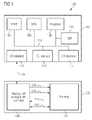
- FIG. 1shows a computer system 100 having a computer arrangement 102 and a memory cell arrangement 120 in accordance with an embodiment.
- the computer arrangement 102may be configured as or may include any device having a processor, e.g., having a programmable processor such as, e.g., a microprocessor (e.g., a CISC (complex instruction set computer) microprocessor or a RISC (reduced instruction set computer) microprocessor).
- a microprocessore.g., a CISC (complex instruction set computer) microprocessor or a RISC (reduced instruction set computer) microprocessor.
- the computer arrangement 102may be configured as or may include a personal computer, a workstation, a laptop, a notebook, a personal digital assistant (PDA), a radio telephone (e.g., a wireless radio telephone or a mobile radio telephone), a camera (e.g., an analog camera or a digital camera), or another device having a processor (such as, e.g., a household appliance (such as, e.g., a washing machine, a dishwashing machine, etc.)).
- PDApersonal digital assistant
- radio telephonee.g., a wireless radio telephone or a mobile radio telephone
- a camerae.g., an analog camera or a digital camera
- a processorsuch as, e.g., a household appliance (such as, e.g., a washing machine, a dishwashing machine, etc.)).
- the computer arrangement 102may include one or a plurality of computer arrangement-internal random access memories (RAM) 104 , e.g., one or a plurality of computer arrangement-internal dynamic random access memories (DRAM), in which, for example, data to be processed may be stored.
- the computer arrangement 102may include one or a plurality of computer arrangement-internal read only memories (ROM) 106 , in which, for example, the program code may be stored, which should be executed by a processor 108 (e.g., a processor as described above), which may also be provided in the computer arrangement 102 .
- ROMread only memories
- one or a plurality of input/output interfaces 110 , 112 , 114(in FIG. 1 , there are shown three input/output interfaces, in alternative embodiments, e.g., one, two, four, or even more than four input/output interfaces may be provided) configured to connect one or a plurality of computer arrangement-external devices (such as, e.g., additional memory, one or a plurality of communication devices, one or a plurality of additional processors) to the computer arrangement 102 , may be provided in the computer arrangement 102 .
- computer arrangement-external devicessuch as, e.g., additional memory, one or a plurality of communication devices, one or a plurality of additional processors
- the input/output interfaces 110 , 112 , 114may be implemented as analog interfaces and/or as digital interfaces.
- the input/output interfaces 110 , 112 , 114may be implemented as serial interfaces and/or as parallel interfaces.
- the input/output interfaces 110 , 112 , 114may be implemented as one or a plurality of circuits, which implements or implement a respective communication protocol stack in its functionality in accordance with the communication protocol which is respectively used for data transmission.
- Each of the input/output interfaces 110 , 112 , 114may be configured in accordance with any communication protocol.
- each of the input/output interfaces 110 , 112 , 114may be implemented in accordance with one of the following communication protocols:
- the first input/output interface 110is a USB interface (in alternative embodiments, the first input/output interface 110 may be configured in accordance with any other communication protocol such as, e.g., in accordance with a communication protocol which has been described above).
- the computer arrangement 102optionally may include an additional digital signal processor (DSP) 116 , which may be provided, e.g., for digital signal processing.
- DSPdigital signal processor
- the computer arrangement 102may include additional communication modules (not shown) such as, e.g., one or a plurality of transmitters, one or a plurality of receivers, one or a plurality of antennas, and so on.
- the computer arrangement 102may also include additional components (not shown), which are desired or required in the respective application.
- circuits or components provided in the computer arrangement 102may be coupled with each other by means of one or a plurality of computer arrangement-internal connections 118 (for example, by means of one or a plurality of computer busses) configured to transmit data and/or control signals between the respectively coupled circuits or components.
- the computer system 100may include the memory cell arrangement 120 .
- the memory cell arrangement 120may in an embodiment be configured as an integrated circuit.
- the memory cell arrangement 120may further be provided in a memory module having a plurality of integrated circuits, wherein at least one integrated circuit of the plurality of integrated circuits includes a memory cell arrangement 120 , as will be described in more detail below.
- the memory modulemay be a stackable memory module, wherein some of the integrated circuit may be stacked one above the other.
- the memory cell arrangement 120is configured as a memory card.
- the memory cell arrangement 120may include a memory cell arrangement controller 122 (for example, implemented by means of hard wired logic and/or by means of one or a plurality of programmable processors, e.g., by means of one or a plurality of programmable processors such as, e.g., one or a plurality of programmable microprocessors (e.g., CISC (complex instruction set computer) microprocessor(s) or RISC (reduced instruction set computer) microprocessor(s)).
- CISCcomplex instruction set computer
- RISCreduced instruction set computer
- the memory cell arrangement 120may further include a memory 124 having a plurality of memory cells.
- the memory 124will be described in more detail below.
- the memory cell arrangement controller 122may be coupled with the memory 124 by means of various connections. Each of the connections may include one or a plurality of lines and may thus have a bus width of one or a plurality of bits.
- an address bus 126may be provided, by means of which one or a plurality of addresses of one or a plurality of memory cells may be provided by the memory cell arrangement controller 122 to the memory 124 , on which an operation (e.g., an erase operation, a write operation, a read operation, an erase verify operation, or a write verify operation, etc.) should be carried out.
- a data write connection 128may be provided, by means of which the information to be written into the respectively addressed memory cell may be supplied by the memory cell arrangement controller 122 to the memory 124 .
- a data read connection 130may be provided, by means of which the information stored in the respectively addressed memory cell may be read out of the memory 124 and may be supplied from the memory 124 to the memory cell arrangement controller 122 and via the memory cell arrangement controller 122 to the computer arrangement 102 , or, alternatively, directly to the computer arrangement 102 (in which case the first input/output interface 110 would directly be connected to the memory 124 ).
- a bidirectional control/state connection 132may be used for providing control signals from the memory cell arrangement controller 122 to the memory 124 or for supplying state signals representing the state of the memory 124 from the memory 124 to the memory cell arrangement controller 122 .
- the memory cell arrangement controller 122may be coupled to the first input/output interface 110 by means of a communication connection 134 (e.g., by means of a USB communication connection).
- a communication connection 134e.g., by means of a USB communication connection.
- the memory 124may include one chip or a plurality of chips. Furthermore, the memory cell arrangement controller 122 may be implemented on the same chip (or die) as the components of the memory 124 or on a separate chip (or die).
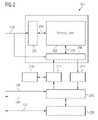
- FIG. 2shows the memory 124 of FIG. 1 in accordance with an embodiment in more detail.
- the memory 124may include a memory cell field (e.g., a memory cell array) 202 having a plurality of memory cells.
- the memory cellsmay be arranged in the memory cell field 202 in the form of a matrix in rows and columns, or, alternatively, for example, in zig zag form. In other embodiments, the memory cells may be arranged within the memory cell field 202 in any other manner or architecture.
- each memory cellmay, for example, be coupled with a first control line (e.g., a word line) and with at least one second control line (e.g., at least one bit line).
- a first control linee.g., a word line
- at least one second control linee.g., at least one bit line
- a row decoder circuit 204configured to select at least one row control line (e.g., a word line) of a plurality of row control lines 206 in the memory cell field 202 may be provided as well as a column decoder circuit 208 configured to select at least one column control line (e.g., a bit line) of a plurality of column control lines 210 in the memory cell field 202 .
- the memory cellsare non-volatile memory cells.
- a “non-volatile memory cell”may be understood as a memory cell storing data even if it is not active.
- a memory cellmay be understood as being not active, e.g., if current access to the content of the memory cell is inactive.
- a memory cellmay be understood as being not active, e.g., if the power supply is inactive.
- the stored datamay be refreshed on a regular timely basis, but not, as with a “volatile memory cell” every few picoseconds or nanoseconds or milliseconds, but rather in a range of hours, days, weeks or months. Alternatively, the data may not need to be refreshed at all in some designs.
- the non-volatile memory cellsmay be, e.g., charge storing random access memory cells (e.g., floating gate memory cells or charge trapping memory cells).
- non-volatile memory cellsmay be used.
- the memory cellsmay be electrically erasable read only memory cells (EEPROM).
- EEPROMelectrically erasable read only memory cells
- each charge trapping memory cellincludes a charge trapping layer structure for trapping electrical charge carriers.
- the charge trapping layer structuremay include one or a plurality of two separate charge trapping regions.
- the charge trapping layer structureincludes a dielectric layer stack including at least one dielectric layer or at least two dielectric layers being formed above one another, wherein charge carriers can be trapped in at least one dielectric layer.
- the charge trapping layer structureincludes a charge trapping layer, which may include or consist of one or more materials being selected from a group of materials that consists of: aluminum oxide (Al 2 O 3 ), yttrium oxide (Y 2 O 3 ), silicon nitride (Si 3 N 4 ), hafnium oxide (HfO 2 ), lanthanum oxide (LaO 2 ), zirconium oxide (ZrO 2 ), amorphous silicon (a-Si), tantalum oxide (Ta 2 O 5 ), titanium oxide (TiO 2 ), and/or an aluminate.
- An example for an aluminateis an alloy of the components aluminum, zirconium and oxygen (AlZrO).
- the charge trapping layer structureincludes a dielectric layer stack including three dielectric layers being formed above one another, e.g., a first oxide layer (e.g., silicon oxide), a nitride layer as charge trapping layer (e.g., silicon nitride) on the first oxide layer, and a second oxide layer (e.g., silicon oxide or aluminum oxide) on the nitride layer.
- a first oxide layere.g., silicon oxide
- a nitride layer as charge trapping layere.g., silicon nitride
- second oxide layere.g., silicon oxide or aluminum oxide
- the charge trapping layer structureincludes two, four or even more dielectric layers being formed above one another.
- the charge trapping layer structuremay include a so-called TANOS layer stack, which may include a substrate, an oxide layer (e.g., silicon oxide) on the substrate (the oxide layer, e.g., having a layer thickness in the range from about 3 nm to about 6 nm), a nitride layer (e.g., silicon nitride) on the oxide layer (the nitride layer, e.g., having a layer thickness in the range from about 3 nm to about 10 nm), a high-k dielectric layer (e.g., having a dielectric constant higher than 3.9) on the nitride layer (the high-k dielectric layer including, e.g., aluminum oxide, and the high-k dielectric layer, e.g., having a layer thickness in the range from about 5 nm to about 15 nm), and a metal gate layer (e.g., made of tantalum nitride (TaN) or another
- the memory cellsmay be multi-bit memory cells.
- multi-bit memory cellis intended to, e.g., include memory cells which are configured to store a plurality of bits by spatially separated electric charge storage regions or current conductivity regions, thereby representing a plurality of logic states.
- the memory cellsmay be multi-level memory cells.
- multi-level memory cellis intended to, e.g., include memory cells which are configured to store a plurality of bits by showing distinguishable voltage or current levels dependent on the amount of electric charge stored in the memory cell or the amount of electric current flowing through the memory cell, thereby representing a plurality of logic states.
- address signalsare supplied to the row decoder circuit 204 and the column decoder circuit 208 by means of the address bus 126 , which is coupled to the row decoder circuit 204 and to the column decoder circuit 208 .
- the address signalsuniquely identify at least one memory cell to be selected for an access operation (e.g., for one of the above described operations).
- the row decoder circuit 204selects at least one row and thus at least one row control line 206 in accordance with the supplied address signal.
- the column decoder circuit 208selects at least one column and thus at least one column control line 210 in accordance with the supplied address signal.
- the electrical voltages that are provided in accordance with the selected operatione.g., for reading, programming (e.g., writing) or erasing of one memory cell or of a plurality of memory cells, are applied to the selected at least one row control line 206 and to the at least one column control line 210 .
- each memory cellis configured in the form of a field effect transistor (e.g., in the case of a charge storing memory cell)
- the respective gate terminalis coupled to the row control line 206 and a first source/drain terminal is coupled to a first column control line 210 .
- a second source/drain terminalmay be coupled to a second column control line 210 .
- a first source/drain terminal of an adjacent memory cellwhich may then, e.g., also be coupled to the same row control line 206 (this is the case, e.g., in a NAND arrangement of the memory cells in the memory cell field 202 ).
- a single row control line 206 and a single column control line 210are selected at the same time and are appropriately driven for reading or programming of the thus selected memory cell.
- itmay be provided to respectively select a single row control line 206 and a plurality of column control lines 210 at the same time for reading or for programming, thereby allowing to read or program a plurality of memory cells at the same time.
- the memory 124includes at least one write buffer memory 212 and at least one read buffer memory 214 .
- the at least one write buffer memory 212 and the at least one read buffer memory 214are coupled with the column decoder circuit 208 .
- reference memory cells 216may be provided for reading the memory cells.
- the data to be programmedmay be received by a data register 218 , which is coupled with the data write connection 128 , by means of the data write connection 128 , and may be buffered in the at least one write buffer memory 212 during the write operation.
- the data read from the addressed memory cell(represented, e.g., by means of an electrical current, which flows through the addressed memory cell and the corresponding column control line 210 , which may be compared with a current threshold value in order to determine the content of the memory cell, wherein the current threshold value may e.g. be dependent from the reference memory cells 216 ) are, e.g., buffered in the read buffer memory 214 during the read operation.
- the result of the comparison und therewith the logic state of the memory cell(wherein the logic state of the memory cell represents the memory content of the memory cell) may then be stored in the data register 218 and may be provided via the data read connection 130 , with which the data register 218 may be coupled.
- the access operationsmay be controlled by a memory-internal controller 220 , which in turn may be controlled by the memory cell arrangement controller 122 by means of the bidirectional control/state connection 132 .
- the data register 218may directly be connected to the memory cell arrangement controller 122 by means of the bidirectional control/state connection 132 and thus directly controlled thereby.
- the memory-internal controller 220may be omitted.
- the memory cells of the memory cell fieldmay be grouped into memory blocks or memory sectors, which may be commonly erased in an erase operation. In an embodiment, there are so many memory cells included in a memory block or memory sector such that the same amount of data may be stored therein as compared with a conventional hard disk memory sector (e.g., 512 byte), although a memory block or memory sector may alternatively also store another amount of data.
- a conventional hard disk memory sectore.g., 512 byte
- peripheral circuitssuch as, e.g., charge pump circuits, etc.
- charge pump circuitsetc.
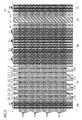
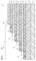
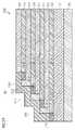
- FIG. 3a layout of the portion 300 of the memory cell field 202 in accordance with an embodiment with a plurality of stacked non-volatile memory cells, is shown in a top view. It should be appreciated that FIG. 3 merely serves as an illustration of fabricating stacked non-volatile memory cells. The individual components shown in FIG. 3 are not true to scale.
- the stacked non-volatile memory cellsare arranged on vertical fins 302 .
- Thirty-two fins 302are shown in FIG. 3 .
- the thirty-two fins 302are arranged substantially parallel to each other on a substrate.
- Selection lines 304(also referred to as word lines 304 ) are arranged in a direction within a plane that is perpendicular to a plane that is, e.g., defined by the longitudinal direction and the height direction of the fins 302 and are serving as lines for selecting a certain memory cell within the large number of thousands or millions or even billions or more of provided memory cells.
- the selection lines 304are arranged in a memory cell region 306 .
- word lines 304are shown on top of the thirty-two fins 302 in a first portion of the memory cell region 306 and additional 44 word lines 304 (10 of them are shown in FIG. 3 ) are provided on the right hand side next to a source line region 308 (which will be described in more detail below) in a second portion of the memory cell region 306 and further additional 44 word lines 304 (10 of them are shown in FIG. 3 ) are provided on the left hand side next to a switch matrix region 310 (which also will be described in more detail below) in a third portion of the memory cell region 306 .
- any number of word lines 304may be provided, e.g., 16 word lines 304 , 32 word lines 304 , 64 word lines 304 , 128 word lines 304 , etc.
- the memory cell field 202may include a plurality of periodically repeatedly occurring portions of the fins 302 , wherein each periodically repeatedly occurring portion may include a memory cell region 306 , a source line region 308 , and a switch matrix region 310 .
- the switch matrix region 310may include a plurality of contact plugs 312 , which will be described in more detail below. At least two bit line contact plugs 312 provide an electrical contact to each of the portion of the fins 302 .
- the bit line contact plugs 312 and the word lines 304can be connected to a readout circuit (not shown), thus enabling individual memory cells to be selected and read out by means of an external circuit, e.g., the readout circuit.
- the readout circuitmay be implemented on the same die as the memory cells.
- a plurality of (e.g., eigth) switch selection lines 314 , 316 , 318 , 320 , 322 , 324 , 326 , 328wherein the shown four first switch selection lines 314 , 316 , 318 , 320 , may be provided to individually address and select a respective memory cell string within a respective fin 302 in the first portion of the memory cell region 306 and the shown four second switch selection lines 322 , 324 , 326 , 328 , may be provided to individually address and select a respective memory cell string within a respective fin 302 in the third portion of the memory cell region 306 .
- first switch selection lines 314 , 316 , 318 , 320may be provided to individually address and select a respective memory cell string within a respective fin 302 in the first portion of the memory cell region 306
- the shown four second switch selection lines 322 , 324 , 326 , 328may be provided to individually address and select a respective memory cell string
- the switch selection lines 314 , 316 , 318 , 320 , 322 , 324 , 326 , 328are arranged in a switch matrix in the switch matrix region 310 and may be used to select a certain memory cell along the fins 302 , as will be described in more detail below.
- a first additional switch selection line(not shown in FIG. 3 ) may be provided between a first selection line 314 of the fin 302 and a first word line 304 of a respective memory cell region 306 including the memory cells.
- the first additional switch selection linemay also be referred to as a string selection line.
- the switch matrixmay include the string selection line.
- a second additional switch selection line 330may be provided (as part of the source line region 308 ) next to the word lines 304 opposite to the first additional switch selection line.
- the second additional switch selection line 330may also be referred to as ground selection line 330 .
- a source line 332may be provided next to the second additional switch selection line 330 in the source line region 308 .
- Next to the source line 332there may be provided another second additional switch selection line 334 adjacent to a first word line 304 of the second portion of the memory cell region 306 .
- the source line 332may be located between two second additional switch selection lines 330 , 334 .
- further word lines 304may be provided next to the other second additional switch selection line 334 , optionally followed by another first additional switch selection line (not shown in FIG. 3 ). In an embodiment, this described structure may be repeatedly provided along the fins 302 .
- the switch selection lines 314 , 316 , 318 , 320 , 322 , 324 , 326 , 328may have associated selection transistors, generally speaking associated selection gates, whose function will be described in more detail below.
- the additional switch selection lines 330 , 334serve as a switch between the memory cells and the transistors of the switch matrix.
- the additional switch selection lines 330 , 334may also have associated selection transistors, generally speaking, associated selection gates.
- the gate lengths of the selection gatesfor example, in the case the first additional switch selection lines are provided, the switch selection lines 314 , 316 , 318 , 320 , 322 , 324 , 326 , 328 , can be designed having significantly smaller gate lengths, since voltages of about V CC may be applied and the isolation of the floating node during programming inhibition may be done by the selection gate of the respective additional switch selection line 330 , 334 .
- the second additional switch selection lines 330 , 334may be separated from each other.
- the second additional switch selection lines 330 , 334can be electrically coupled with one another, in other words, the second additional switch selection lines 330 , 334 , can be short-circuited.
- the additional switch selection lines 330 , 334represent a gate length that is greater than the gate length of the switch selection lines 314 , 316 , 318 , 320 , 322 , 324 , 326 , 328 , in order to reduce the leakage current to ensure high boost voltage in the NAND string during program inhibit.
- the additional switch selection lines 330 , 334may have a gate length in the range of about 150 nm to about 250 nm, e.g., in the range of about 175 nm to about 225 nm, e.g. of about 200 nm.
- the switch selection lines 314 , 316 , 318 , 320 , 322 , 324 , 326 , 328may have a gate length in the range of about 50 nm to about 130 nm, e.g., in the range of about 75 nm to about 120 nm, e.g., of about 100 nm.
- the source line 332may have a width in a range of about 100 nm to about 300 nm.
- the additional switch selection lines 330 , 334may respectively include a charge trapping layer, whereas in an alternative embodiment, the additional switch selection lines 330 , 334 , have no charge trapping layers.
- the switch selection lines 314 , 316 , 318 , 320 , 322 , 324 , 326 , 328may respectively include a charge trapping layer, whereas in an alternative embodiment, the switch selection lines 314 , 316 , 318 , 320 , 322 , 324 , 326 , 328 , have no charge trapping layers.
- the programming of a memory cell of the memory cell field 202can be carried out as follows:
- the bit line of the memory cell to be programmedmay be provided with, e.g., 0 V
- the word line of the memory cell to be programmedmay be provided with, e.g., +25 V.
- the directly adjacent bit lines of the bit line of the memory cell to be programmedmay be provided with, e.g., 3.3 V.
- the additional switch selection lines 330 , 334may be provided with, e.g., 3.3 V.
- the other word lines 304 corresponding to the memory cells not to be programmedmay be provided with a pass voltage of, e.g., 10 V.
- an additional switch matrix formed by additional switch selection linesmay be arranged between the source line 332 and the second additional switch selection line (e.g., in a similar manner as described above, four switch selection lines) and the source line 332 and the other second additional switch selection line (e.g., in a similar manner as described above, four switch selection lines), respectively.
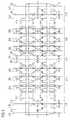
- FIG. 4shows an equivalent circuit diagram of a portion of a memory cell field of FIG. 2 corresponding to the top view of FIG. 3 in accordance with an embodiment.
- the equivalent circuit diagramshows the memory cells 402 of the memory cell region 306 , wherein, e.g., the gate terminals of transistors forming the memory cells 402 are coupled with the word lines 304 .
- switch selection gatese.g., implemented as transistors, e.g. implemented as field effect transistors, e.g., implemented as fin field effect transistors
- 404 , 406 , 408 , 410 , 412 , 414 , 416 , 418are provided in the switch matrix region 310 to form the switch matrix.
- the gate terminal of a respective transistor of the transistors forming the switch selection gates 404 , 406 , 408 , 410 , 412 , 414 , 416 , 418may be coupled with a respective one of the switch selection lines 314 , 316 , 318 , 320 , 322 , 324 , 326 , 328 .
- each switch selection gate 404 , 406 , 408 , 410 , 412 , 414 , 416 , 418is configured to select a respective one of a plurality of memory cell strings 420 , 422 , 424 , 426 , 428 , 430 , 432 , 434 , in other words a respective one of a plurality of memory cells 402 being serially source-to-drain coupled with each other.
- each memory cell string 420 , 422 , 424 , 426 , 428 , 430 , 432 , 434is connected between a respective switch selection gate 404 , 406 , 408 , 410 , 412 , 414 , 416 , 418 , and a gate (e.g., implemented as a transistor, e.g., implemented as a field effect transistor, e.g., implemented as a fin field effect transistor) 436 , e.g., the gate terminal of which may be connected to the second additional switch selection line 330 or the other second additional switch selection line 334 , for example.
- a gatee.g., implemented as a transistor, e.g., implemented as a field effect transistor, e.g., implemented as a fin field effect transistor
- normally-on structures 438e.g. normally-on transistors may be provided in the switch matrix region 310 , as shown in FIG. 4 . All elements shown in FIG. 4 may be implemented in one respective fin structure 302 .
- each fin structure 302may include a plurality of memory cell strings 420 , 422 , 424 , 426 , 428 , 430 , 432 , 434 , for example, which may be formed in a stacked manner above one another, as will be described in more detail below.
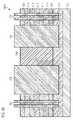
- FIG. 5shows a portion 500 of the memory cell field 202 in a cross sectional view in accordance with an embodiment.
- the cross sectional viewis chosen in a direction perpendicular to the semiconductor surface of the substrate (e.g., the wafer) and along a word line 304 .
- the portion 500 of the memory cell field 202may be arranged on a semiconductor substrate 502 .
- the semiconductor substrate 502may be part of one or more semiconductor wafers, e.g., of one or more semiconductor wafers including semiconductor material, an insulating layer and another semiconductor layer on top of the insulating layer.
- the one or more semiconductor layersmay be formed by one or more silicon on insulator (SOI) semiconductor wafers.
- SOI semiconductor wafersmay be coupled together by means of one or more wafer bonding processes.
- each fin structure 504may include a part of the semiconductor substrate 502 , a first insulating layer 506 arranged on or above the upper surface of the semiconductor substrate 502 , a first semiconductor layer 508 arranged on or above the upper surface of the first insulating layer 506 , a second insulating layer 510 arranged on or above the upper surface of the first semiconductor layer 508 , a second semiconductor layer 512 arranged on or above the upper surface of the second insulating layer 510 , a third insulating layer 514 arranged on or above the upper surface of the second semiconductor layer 512 , a third semiconductor layer 516 arranged on or above the upper surface of the third insulating layer 514 , a fourth insulating layer 518 arranged on or above the upper surface of the third semiconductor layer 516 , and a fourth semiconductor layer 520 arranged on or above the upper surface of the fourth insulating layer 518 .
- two, three, or even more than four semiconductor layersre
- each fin structure 504thus may include four semiconductor fins formed by the respective semiconductor layers 508 , 512 , 516 , 520 , the semiconductor fins being electrically isolated from each other by means of the respective insulating layers 506 , 510 , 514 , 518 .
- a portion of the upper surface of the substrate 502 between the fin structures 504may be exposed during the manufacturing process, in which the fin structures 504 are formed, as will be described in more detail below.
- a patterned charge storage layer structure 522may be provided.
- the charge storage layer structure 522may cover the insulating layers 506 , 510 , 514 , 518 , the semiconductor layers 508 , 512 , 516 , 520 , as well as the exposed surface portions of the surface of the substrate 502 between the fin structures 504 .
- the charge storage layer structure 522may be a floating gate structure including an insulating layer, e.g., a tunnel oxide layer (e.g., having a thickness in the range from about 5 nm to about 10 nm, e.g., having a thickness of about 5 nm), the insulating layer covering the insulating layers 506 , 510 , 514 , 518 , the semiconductor layers 508 , 512 , 516 , 520 , as well as the exposed surface portions of the surface of the substrate 502 between the fin structures 504 .
- the floating gate structureincludes a floating gate layer, e.g., made of polysilicon, being provided on the insulating layer.
- the floating gate layermay include metallically conductive portions forming the floating gates of the respective memory cells, and isolating portions to isolate respectively adjacent floating gates of adjacent memory cells.
- the floating gate structuremay include another insulating layer, e.g., a gate oxide layer (e.g., having a thickness in the range of 5 nm to 15 nm), being provided on the floating gate layer.
- the other insulating layermay include a plurality of dielectric layers, e.g. an ONO layer stack (e.g., having an oxide layer (e.g., silicon oxide) e.g., having a layer thickness of about 5 nm on the floating gate layer, a nitride layer (e.g.
- the other insulating layermay include a high-k material (e.g., aluminum oxide) e.g., having a layer thickness in the range from about 5 nm to about 15 nm).
- a high-k materiale.g., aluminum oxide
- the fin of the uppermost layermay have an additional buffer oxide layer on top of the fin but below the charge storage layer.
- the memory cells of the top most layerhas only two sidewalls as active area while the conduction via the top layer is suppressed to a large degree. This may ensure more homogeneity of the electrical behavior of the top most active layer compared to the layers below.
- the charge storage layer structure 522may be a nanocrystalline type layer structure having nanocrystals embedded in a dielectric, the nanocrystals being configured to store electrical charges.
- the charge storage layer structure 522may be a charge trapping layer structure.
- the charge trapping layer structuremay include a dielectric layer stack including one or a plurality of at least two dielectric layers being formed above one another, wherein charge carriers can be trapped in at least one of the at least two dielectric layers.
- the charge trapping layer structureincludes a charge trapping layer, which may include or consist of one or more materials being selected from a group of materials that consists of: aluminum oxide (Al 2 O 3 ), yttrium oxide (Y 2 O 3 ), silicon nitride (Si 3 N 4 ), hafnium oxide (HfO 2 ), lanthanum oxide (LaO 2 ), zirconium oxide (ZrO 2 ), amorphous silicon (a-Si), tantalum oxide (Ta 2 O 5 ), titanium oxide (TiO 2 ), and/or an aluminate.
- An example for an aluminateis an alloy of the components aluminum, zirconium and oxygen (AlZrO).
- the charge trapping layer structuremay include a dielectric layer stack including three dielectric layers being formed above one another, namely a first oxide layer (e.g., silicon oxide), a nitride layer as charge trapping layer (e.g., silicon nitride) on the first oxide layer, and a second oxide layer (e.g., silicon oxide or aluminum oxide) on the nitride layer.
- a first oxide layere.g., silicon oxide
- a nitride layer as charge trapping layere.g., silicon nitride
- second oxide layere.g., silicon oxide or aluminum oxide
- the ONO layer stackmay be conformally deposited on the sidewalls of the fins and optionally in addition on the upper surface of the fins, in other words, on the vertical sidewalls of the insulating layers 506 , 510 , 514 , 518 and the semiconductor layers 508 , 512 , 516 , 520 , e.g., parallel to a plane that is defined by the longitudinal direction and the height direction of the fins.
- the charge trapping layer structuremay include a so-called TANOS layer stack, which may include a substrate, an oxide layer (e.g. silicon oxide) on the substrate (the oxide layer e.g.
- a nitride layere.g., silicon nitride
- the oxide layerthe nitride layer, e.g., having a layer thickness in the range from about 3 nm to about 10 nm
- a high-k dielectric layere.g., having a dielectric constant higher than 3.9
- the high-k dielectric layerincluding, e.g., aluminum oxide, and the high-k dielectric layer, e.g., having a layer thickness in the range from about 5 nm to about 15 nm
- a metal gate layere.g., made of tanatlum nitride (TaN) or another metal having a high work function
- the charge trapping layer structure 522may include two, four or even more dielectric layers being formed above one another.
- a control gate layer 524may be provided, e.g., made of polysilicon or a metal such as copper or aluminum.
- the control gate layer 524may be conformally deposited on the patterned charge storage layer structure 522 .
- each fin structure 504may extend from a top surface of the control gate layer 524 through the charge storage layer structure 522 , the plurality of semiconductor layers 508 , 512 , 516 , 520 , and through the plurality of insulating layers 506 , 510 , 514 , 518 , at least into the bottommost insulating layer, i.e., the first insulating layer 506 , or even into the semiconductor substrate 502 , so that a bottom surface 526 may be formed at a predetermined fin depth.
- an additional dielectric layermay be disposed on the bottom surface 526 , e.g., in case that the structure of the semiconductor substrate 502 is also used as a respective NAND string of memory cells. In an embodiment, however, the patterned charge storage layer structure 522 is disposed directly on the bottom surface 526 .
- the patterned charge storage layer structure 522may be arranged in a direction substantially perpendicular to the orientation of the fins.
- the control gate layer 524 and, after patterning, the word lines formed by the patterned control gate layer 524are arranged on the charge storage layer structure 522 .
- the word lines 304may have sidewalls (not shown in FIG. 5 ) that are optionally covered by a spacer oxide layer, which protects the active regions of the transistors to be formed during the implantation of doping atoms for optionally forming source/drain regions (not shown for reasons of clarity).
- the source/drain regionsmay be formed in the semiconductor layers 508 , 512 , 516 , 520 , in the fins outside the word lines 304 and the optional spacer oxide layer.
- each fin structure 504may include four strings of serially connected memory cells being formed by fin field effect transistors (FinFET).
- the FinFETsare electrically isolated from the semiconductor substrate 502 e.g. by means of one or more of the insulating layers 506 , 510 , 514 , 518 .
- the FinFETsare attached to the bottommost layer of the charge storage layer structure 522 , e.g., to the tunnel oxide layer (e.g., in the case of a floating gate structure) or to the first oxide layer (e.g., in the case of a charge trapping gate structure).
- the tunnel oxide layere.g., in the case of a floating gate structure
- the first oxide layere.g., in the case of a charge trapping gate structure
- an arbitrary number of finsmay be formed one above the other (in the height direction), each fin being isolated from the adjacent one of the fins by means of a respective insulating layer, thereby forming an arbitrary number of memory cell strings, wherein the memory cells of a respective memory cell string may be connected with each other in accordance with a NAND type connection scheme. If a channel is formed allowing a current flow through a respective FinFET, the current flows through the fin in a direction which is perpendicular to the paper plane of FIG. 5 .
- the charge storage layer structure 522may provide non-volatile storage properties.
- the memory cell fieldmay include a further memory cell string, the memory cells of which may be connected with each other in accordance with a NAND type connection scheme.
- the further memory cell stringmay be formed by the semiconductor structure formed below the first insulating layer 506 , i.e., by the fin-shaped portion of the semiconductor substrate 502 .
- theremay be, e.g., five memory cells formed one above the other with the fin-shaped portion of the bulk material, i.e., with the fin-shaped portion of the semiconductor substrate 502 , providing the further NAND memory cell string.
- a method for manufacturing a memory cell arrangement in accordance with an embodimentwill be described in the following.
- the following processesalso further illustrate possible materials for the individual components and respective geometrical characteristics.
- a method for forming a non-volatile stacked memory cell as shown in FIG. 5is illustrated.
- a wafer arrangement 600 including a plurality of wafersis shown.
- a plurality of silicon on insulator wafer(SOI wafer) is provided, e.g., four SOI wafers 602 , 604 , 606 , 608 .
- the SOI wafers 602 , 604 , 606 , 608 of the wafer arrangement 600may be single crystalline SOI wafers or polycrystalline wafers.
- the wafer arrangement 600may be manufactured, e.g., by wafer bonding processes of the four SOI wafers 602 , 604 , 606 , 608 .
- any other suitable processcan be used to manufacture the stack of multiple SOI wafers 602 , 604 , 606 , 608 .
- any numbere.g., up to 10 wafers (e.g. SOI wafers) may be stacked above one another.
- a bottommost first SOI wafer 602has a carrier, e.g., semiconductor carrier, e.g., a semiconductor substrate, e.g., the semiconductor substrate 502 (e.g., made of silicon), the first insulating layer 506 arranged on or above the upper surface of the semiconductor substrate 502 , and the first semiconductor layer 508 arranged on or above the upper surface of the first insulating layer 506 .
- a second SOI wafer 604may be disposed on or above the upper surface of the first semiconductor layer 508 .
- the second SOI wafer 604may include the second insulating layer 510 arranged on or above the upper surface of the first semiconductor layer 508 and the second semiconductor layer 512 arranged on or above the upper surface of the second insulating layer 510 .
- a third SOI wafer 606may be disposed on or above the upper surface of the second semiconductor layer 512 .
- the third SOI wafer 606may include the third insulating layer 514 arranged on or above the upper surface of the second semiconductor layer 512 and the third semiconductor layer 516 arranged on or above the upper surface of the third insulating layer 514 .
- a fourth SOI wafer 608may be disposed on or above the upper surface of the third semiconductor layer 516 .
- the fourth SOI wafer 608may include the fourth insulating layer 518 arranged on or above the upper surface of the third semiconductor layer 516 and the fourth semiconductor layer 520 arranged on or above the upper surface of the fourth insulating layer 518 .
- the semiconductor layers 508 , 512 , 516 , 520may be made of silicon (e.g., p-doped silicon) and the insulating layers 506 , 510 , 514 , 518 , may be made of an oxide such, as e.g., silicon dioxide.
- the semiconductor layers 508 , 512 , 516 , 520 , and the insulating layers 506 , 510 , 514 , 518may have a respective thickness in the range of about 20 nm to about 1 ⁇ m.
- the periphery area of the memory cell arrangement to be manufacturede.g., of the NAND memory cell arrangement to be manufactured, according to a CMOS process in accordance with an embodiment, high-voltage devices such as charge pumps, may be provided.
- the parasitic capacitance of such a deviceshould be small. Therefore, an SOI wafer stack is not used as the substrate for the CMOS in the periphery area. In an embodiment, the SOI stack may be removed in the CMOS periphery area.
- a thin silicon dioxide layermay be formed on the remaining semiconductor substrate 502 in the periphery area as well as on the top surface of the wafer arrangement 600 , in other words on the upper surface of the fourth semiconductor layer 520 and on the sidewalls of the step between the upper surface of the fourth semiconductor layer 520 and the exposed semiconductor substrate 502 in the periphery area.
- the silicon dioxide layermay have a thickness in the range of about 50 nm to about 500 nm.
- the silicon dioxide layermay be anisotropically etched from the top surface of the semiconductor substrate 502 in the CMOS periphery area.
- the array and a three dimensional (3D) switch matrixwhich will be described in more detail below, as well as the side of the SOI stack part is covered by the silicon dioxide.
- epitaxial silicon(Epi-Si) may be selectively deposited in the CMOS periphery area.
- the thickness of the Epi-Simay be given by the height of the SOI stack so that the entire wafer arrangement 600 may have the same thickness all over the NAND memory area and the CMOS periphery area.
- the shallow trench isolation (STI) in the CMOS periphery areamay be formed in a conventional way.
- a thermal silicon oxide layermay then be formed on the upper surface of the structure that results in the processes described above.
- the thermal silicon oxide layerhas several functions. It acts as a scattering oxide for the implant processes that follow and as a pad oxide for the silicon nitride hardmask.
- the well doping(which may be adjusted using ion implantation, for example) for the three dimensional structure may be special compared to a standard NAND process flow for FinFETs.
- the CMOS well implantsmay correspond to the standard CMOS well implants.
- all four semiconductor layers 508 , 512 , 516 , 520are implanted with doping atoms such as boron (B).
- the switch matrix region 310which also may have a three dimensional structure (in one embodiment, the switch matrix region 310 is provided in the fins 504 ), will be described in more detail below.
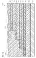
- FIG. 7shows a schematic top view 700 of a portion of the switch matrix region 310 in accordance with an embodiment at a first state of manufacturing showing the fins 302 .
- FIG. 7shows a plurality of cross sections, the corresponding cross sectional views of which will be described in more detail below.
- FIG. 8shows a cross sectional view 800 of a portion of the switch matrix region 310 of FIG. 7 taken along cross section A of FIG. 7 in accordance with an embodiment at a first time of manufacturing.
- a staircase structure 804may be formed (e.g., etched) into the SOI wafers, in other words, into the wafer arrangement 600 of FIG. 6 .
- the formation of the staircase structure 804may be realized, e.g., by means of a process sequence of lithographic processes and etching processes (e.g., anisotropic etching processes such as e.g. reactive ion etching processes (RIE)).
- RIEreactive ion etching processes
- the formation of the staircase structure 804may be realized, e.g., by means of a process sequence of lithographic, etching, spacer formation, and etching processes. The processes will be described in more detail below.
- an insulating layer 802(which may be used as an auxiliary mask layer such as, e.g., as a hard mask layer), e.g., made of silicon dioxide, silicon nitride or carbon, may be deposited on the upper surface of the fourth semiconductor layer 520 .
- a first partial staircase structure 806may be formed by etching the layer stack of the wafer arrangement 600 in the switch matrix region 310 , e.g., in an area of the second switch selection line 316 down to the third semiconductor layer 516 , thereby exposing the upper surface 808 thereof as well as sidewall portions of the fourth insulating layer 518 and the fourth semiconductor layer 520 .
- a first step of the staircase structure 804may be formed which may include the exposed upper surface 808 of the third semiconductor layer 516 as the main portion of the first step and the sidewall portions of the fourth insulating layer 518 and the fourth semiconductor layer 520 as the sidewall portion of the first step.
- a second partial staircase structure 810may be formed by further etching the layer stack of the wafer arrangement 600 in the switch matrix region 310 , e.g. in an area of the third switch selection line 318 down to the second semiconductor layer 512 , thereby exposing the upper surface 812 thereof as well as sidewall portions of the third insulating layer 514 and the third semiconductor layer 516 .
- a second step of the staircase structure 804may be formed which may include the exposed upper surface 812 of the second semiconductor layer 512 as the main portion of the second step and the sidewall portions of the third insulating layer 514 and the third semiconductor layer 516 as the sidewall portion of the second step.
- a third partial staircase structure 814may be formed by further etching the layer stack of the wafer arrangement 600 in the switch matrix region 310 , e.g. in an area of the fourth switch selection line 320 down to the first semiconductor layer 508 , thereby exposing the upper surface 816 thereof as well as sidewall portions of the second insulating layer 510 and the second semiconductor layer 512 .
- a third step of the staircase structure 804may be formed which may include the exposed upper surface 816 of the first semiconductor layer 508 as the main portion of the third step and the sidewall portions of the second insulating layer 510 and the second semiconductor layer 512 as the sidewall portion of the second step.
- FIG. 9shows a cross sectional view 900 of a portion of the switch matrix region 310 of FIG. 7 taken along cross section A of FIG. 7 in accordance with an embodiment at a second time of manufacturing.
- an ion implantation processmay be carried out using a lithographic mask (e.g., a photo resist mask) which may be opened in a staircase structure area 902 , wherein the ion implantation process may include an implantation of, e.g., n-type doping atoms (also referred to as donator atoms, e.g. phosphorous) using a sequence of threshold voltage implantation processes.
- the implantation energymay be selected such that the portions not covered by the lithographic mask of all semiconductor layers 508 , 512 , 516 , 520 may be doped with the n-type doping atoms.
- the implantation energy of each single implant stepmay be selected according to the position of the semiconductor layers 508 , 512 , 516 , 520 to be in the range from about 10 keV to about 1000 keV. Furthermore, the concentration of the doping atoms in the implanted regions may be selected to be in the range from about 10 17 cm ⁇ 3 to about 5*10 17 cm ⁇ 3 . In this way, doped regions 904 , 906 , 908 , 910 , may be formed in the semiconductor layers 508 , 512 , 516 , 520 , in the staircase structure area 902 .
- phosphorous atomsmay be used as doping atoms to form the doped regions 904 , 906 , 908 , 910 .
- arsenic atoms or antimon atomsmay be used as doping atoms to form the doped regions 904 , 906 , 908 , 910 .
- the implantation energies used in accordance with the described embodimentsare merely to be understood as examples and serve for illustration purposes. The implantation energies used in accordance with the described embodiments may be dependent on the respectively used materials and the layer thicknesses of the respectively provided layers.
- a shallow ion implantationmay be carried out to provide a counterdoping of portions of the doped regions 904 , 906 , 908 , 910 .
- the implantation energy in the shallow ion implantationmay be set such that the doping atoms may be implanted in the respective uppermost semiconductor layer 508 , 512 , 516 , 520 , which is immediately beneath the uppermost and exposed insulating layer.
- only one of the semiconductor layers 508 , 512 , 516 , 520is respectively doped with doping atoms, and the portions of the semiconductor layer 508 , 512 , 516 , 520 , which are arranged below a further insulating layer or another semiconductor layer 508 , 512 , 516 , 520 , are not doped.
- the respective uppermost semiconductor layer 508 , 512 , 516 , 520is locally counterdoped in this implantation process, thereby forming counterdoped regions 912 , 914 , 916 , 918 .
- the counterdoped regions 912 , 914 , 916 , 918may be laterally displaced with respect to each other and may be arranged in different layers, in other words, also vertically displaced.
- the shallow ion implantationmay be implemented as a p-type threshold voltage implantation.
- the counterdoped regions 912 , 914 , 916 , 918may be doped in such a manner that normally-off transistors may be formed using the counterdoped regions 912 , 914 , 916 , 918 , as the active areas and thus as the channel regions.
- the implantation energy for the counter-implantationmay be selected to be in the range from about 1 keV to about 10 keV.
- the concentration of the doping atoms in the counterdoped regions 912 , 914 , 916 , 918may be selected to be in the range from about 2*10 17 cm ⁇ 3 to about 10 18 cm ⁇ 3 .
- the counterdoped regions 912 , 914 , 916 , 918may be formed in the semiconductor layers 508 , 512 , 516 , 520 , within and thus in the result next to the doped regions 904 , 906 , 908 , 910 .
- boron atomsmay be used as doping atoms to form the counterdoped regions 912 , 914 , 916 , 918 .
- the implantation energy used for the counter-implantationmay be selected to be smaller than the implantation energy used for the formation of the doped regions 904 , 906 , 908 , 910 .
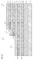
- FIG. 10shows a cross sectional view 1000 of a portion of the switch matrix region 310 of FIG. 7 taken along cross section A of FIG. 7 in accordance with an embodiment at a third time of manufacturing.
- the space above the staircase structure 804may be “filled” with insulating material 1002 .
- Thismay be carried out by depositing insulating material (e.g., an oxide material such as, e.g., silicon oxide) on the surface of the previously formed staircase structure 804 .
- the upper surface of the insulating materialmay be planarized, e.g. by means of a polishing process, e.g., a chemical mechanical polishing (CMP) process.
- CMPchemical mechanical polishing
- an auxiliary mask layer 1004such as, e.g., a hard mask layer 1004 (e.g., made of a nitride (e.g., silicon nitride) or a carbide (e.g., silicon carbide) may be deposited.
- the auxiliary mask layer 1004may be provided as a mask for a following gate contact etching process, as will be described in more detail below.
- FIG. 11shows a cross sectional view 1100 of a portion of the switch matrix region 310 of FIG. 7 taken along cross section B of FIG. 7 in accordance with an embodiment at the third time of manufacturing.
- the fin structures 504 and therewith in the fins 504 active area stringsmay be formed which may run perpendicular to the staircase structure 804 (in FIG. 11 , the active area strings run perpendicular to the paper plane).
- an anisotropic etching processsuch as, e.g., a reactive ion etching (RIE) process
- RIEreactive ion etching
- FIG. 12shows a cross sectional view 1200 of a portion of the switch matrix region 310 of FIG. 7 taken along cross section D of FIG. 7 in accordance with an embodiment at the third time of manufacturing.
- the structuremay include only the semiconductor substrate 502 and the first insulating layer 506 arranged on or above the upper surface of the semiconductor substrate 502 .
- FIG. 13shows a cross sectional view 1300 of a portion of the switch matrix region 310 of FIG. 7 taken along cross section C of FIG. 7 in accordance with an embodiment at the third time of manufacturing.
- the bottommost counterdoped region 918is covered by the insulating material 1002 . It should be noted that the other counterdoped region 912 , 914 , 916 , are positioned behind the bottommost counterdoped region 918 seen in a direction perpendicular to the paper plane of FIG. 13 .
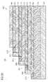
- FIG. 14shows a schematic top view 1400 of a portion of the switch matrix region 310 in accordance with an embodiment after the manufacturing of word lines 304 .
- FIG. 15shows a cross sectional view 1500 of a portion of the switch matrix region 301 of FIG. 13 taken along cross section E of FIG. 13 in accordance with an embodiment after the manufacturing of word lines 304 .
- FIG. 16shows a cross sectional view 1600 of a portion of the switch matrix region 310 of FIG. 13 taken along cross section F of FIG. 13 in accordance with an embodiment after the manufacturing of word lines 304 .
- a layer stack which will form a charge storage layer structure of the memory cells to be formed in the memory cell region 306is deposited.
- a charge trapping layer stack as described abovemay be deposited on the formed fin structures.
- a first oxide layer 1602e.g. made of silicon oxide
- a charge trapping layer 1604e.g. a nitride layer 1604 (e.g., made of silicon nitride) may be (e.g., conformally) deposited on the first oxide layer 1602 .
- a second oxide layer 1606e.g.
- electrically conductive material 1608(which will form the gate contacts and the word lines 304 ) such as, e.g., polysilicon (doped or undoped) may be deposited on the second oxide layer 1606 and thus between and above the fin structures 504 and therewith illustratively being arranged next to the sidewalls of the semiconductor layers 508 , 512 , 516 , 520 and the insulating layers 510 , 514 518 , 802 .
- the electrically conductive material 1608serves as the gates for the memory cells (in the memory cell region 306 ) as well as for the switch transistors formed in the switch matrix region 310 . Then, using a lithographic process and an etching process, for example, the charge storage layer stack and the electrically conductive material 1608 are patterned such that they form the charge storage structure and the gates (and the word lines 304 and the switch selection lines 314 , 316 , 318 , 320 , 322 , 324 , 326 , 328 ).
- FIG. 17shows another cross sectional view 1700 of a portion of a switch matrix region of FIG. 14 in accordance with an embodiment after the manufacturing of bit lines.
- FIG. 17shows another cross sectional view 1700 of a portion of a switch matrix region of FIG. 14 in accordance with an embodiment after the manufacturing of bit lines.
- middle-of-line (MOL) processesmay be carried out to the resulting structure as shown in FIGS. 15 and 16 .
- a dielectric material 1702(e.g., a so-called poly-metal-dielectric (PMD) layer) may be deposited (e.g., by means of a chemical vapor deposition (CVD) process or a physical vapor deposition (PVD) process) on the auxiliary mask layer 1004 and the remaining exposed portions of the structure as shown in FIGS. 15 and 16 .
- a dielectric material 1702e.g., a so-called poly-metal-dielectric (PMD) layer
- CVDchemical vapor deposition
- PVDphysical vapor deposition
- an oxidesuch as, e.g., silicon oxide may be used for the dielectric material 1702 , although any other suitable dielectric material may be used in an alternative example.
- contact holes 1704may be formed (e.g., etched, e.g., by means of an anisotropic etching such as, e.g., by means of RIE etching) in the area above the counterdoped regions 912 , 914 , 916 , 918 , and between the switch selection lines 314 , 316 , 318 , 320 , 322 , 324 , 326 , 328 , thereby exposing respective upper surface portions of the counterdoped regions 912 , 914 , 916 , 918 .
- anisotropic etchingsuch as, e.g., by means of RIE etching
- an n + -implantation processmay be carried out through the contact holes 1704 using n-type doping atoms (e.g., phosphorous atoms, arsenic atoms, or antimon atoms may be used) to form n + -doped regions 1706 within the exposed counterdoped regions 912 , 914 , 916 , 918 which may serve as bit line contact plugs for the bit line connections.
- n-type doping atomse.g., phosphorous atoms, arsenic atoms, or antimon atoms may be used
- the contact holes 1704may be filled with electrically conductive material 1708 such as, e.g., tungsten (W) or tungsten silicide (WSi) or any other suitable material.
- a metal layermay be deposited (e.g., using a CVD or PVD) and then patterned such that bit lines 1710 , which may be respectively electrically coupled to the electrically conductive material 1708 filled into the contact holes 1704 .
- bit lines 1710may be respectively electrically coupled to the electrically conductive material 1708 filled into the contact holes 1704 .
- BEOLback-end-of-line
- FIG. 18shows yet another cross sectional view 1800 of a portion of a switch matrix region of FIG. 14 in accordance with an embodiment after the manufacturing of bit lines.
- FIG. 18shows both sides of the switch matrix region 310 together with additional counterdoped regions 1802 , 1804 , 1806 which are formed in a similar manner as the counterdoped regions 912 , 914 , 916 , 918 .
- the switch matrix region 310 in accordance with an embodimentis completed.
- the metallization of the memory cell arrangementmay be provided such that the bit lines are provided in the so called metallization plane 0 (i.e., in the first metallization plane above the word lines), and the bit lines run, e.g., perpendicular to the main direction of the word lines.
- supply linesmay be provided in the so called metallization plane 1 (i.e., in the second metallization plane above the word lines, sometimes referred to as Metal 1) for contacting and reducing the RC delay of the well contacts (not shown), the source line 116 and the select gates.
- one or more additional metallization planesmay be provided above the mentioned metallization planes.
- an arbitrary number of metallization planesmay be provided and the above mentioned lines may be provided in different metallization planes than described above.
- bit linesmay be arranged in the metallization plane 1 (i.e., in the second metallization plane above the word lines) and may be connected with the contact plugs, wherein the metallization plane 0 (i.e., the first metallization plane above the word lines, sometimes referred to as Metal 0) may provide the well contacts and the supply lines for the select gates and a low ohmic source line further decreasing the ohmic resistance of the source line.
- the metallization plane 0i.e., the first metallization plane above the word lines, sometimes referred to as Metal 0
- FIG. 19shows a cross sectional view 1900 of a portion of the switch matrix region 310 in accordance with another embodiment after the manufacturing of bit lines.
- This embodimentis similar to the embodiments described above and is manufactured in a similar manner. Therefore, in order to avoid unnecessary repetition, only the differences of this embodiment compared with the embodiments described above will be explained in the following.
- a wider switch selection line 1902(wider than the select switch selection lines 314 , 316 , 318 , 320 , 322 , 324 , 326 , 328 ) may additionally be provided for decoding as a commonly shared select gate.
- smaller select gatesand thus also narrower switch selection lines 1904 , 1906 , 1908 , 1910 compared with the width of the switch selection lines 314 , 316 , 318 , 320 , 322 , 324 , 326 , 328 may be provided) for decoding.
- Thismay save chip area for the memory cell field 202 .
- a low resistancemay be provided (and thus higher read currents) due to shorter memory cell strings.
- FIG. 20shows a cross sectional view 2000 of a portion of the switch matrix region 310 in accordance with yet another embodiment at a first time of the manufacturing.
- This embodimentis similar to the embodiments described above and is manufactured in a similar manner. Therefore, in order to avoid unnecessary repetition, only the differences of this embodiment compared with the embodiments described above will be explained in the following.
- This embodimentmainly differs in the way of manufacturing the staircase structure 804 , as will be described in more detail below.
- the steps of the staircase structure in accordance with this embodimentis manufactured differently after a doping of all semiconductor layers 508 , 512 , 516 , 520 , in the staircase structure area 902 .
- the dopingmay be carried out using an ion implantation process.
- the ion implantation processmay include an implantation of, e.g., n-type doping atoms (also referred to as donator atoms, e.g., phosphorous) using a sequence of threshold voltage implantation processes.
- the implantation energymay be selected such that the portions not covered by the lithographic mask of all semiconductor layers 508 , 512 , 516 , 520 may be doped with the n-type doping atoms.
- the implantation energymay be selected to be in the range from about 10 keV to about 1000 keV.
- the concentration of the doping atoms in the implanted regionsmay be selected to be in the range from about 10 17 cm ⁇ 3 to about 5*10 17 cm ⁇ 3 .
- doped regions 2002 , 2004 , 2006 , 2008may be formed in the semiconductor layers 508 , 512 , 516 , 520 , in the staircase structure area 902 .
- phosphorous atomsmay be used as doping atoms to form the doped regions 2002 , 2004 , 2006 , 2008 .
- arsenic atoms or antimon atomsmay be used as doping atoms to form the doped regions 2002 , 2004 , 2006 , 2008 .
- FIG. 21shows a cross sectional view 2100 of a portion of a switch matrix region 310 in accordance with yet another embodiment at a second time of the manufacturing.
- a first step 2102may be formed, e.g. using a lithographic process and an etching process (e.g., an anisotropic etching process such as e.g. a RIE process), wherein the etching process may be stopped on the upper surface of the fourth insulating layer 518 , which is thereby exposed.
- a shallow ion implantationmay be carried out to provide a counterdoping of portions of the doped regions 2006 , 2008 .
- the implantation energy in the shallow ion implantationmay be set such that the doping atoms may be implanted in the respective uppermost semiconductor layer 516 , 520 , which is immediately beneath the uppermost and exposed insulating layers.
- the respective uppermost semiconductor layer 516 , 520is locally counterdoped in this implantation process, thereby forming counterdoped regions 2104 , 2106 .
- the counterdoped regions 2104 , 2106may be laterally displaced with respect to each other and may be arranged in different layers, e.g.
- the shallow ion implantationmay be implemented as a p-type threshold voltage implantation.
- the counterdoped regions 2104 , 2106may be doped in such a manner that normally-off transistors may be formed using the counterdoped regions 2104 , 2106 , as the active areas and thus as the channel regions of the respective transistors to be formed.
- the implantation energy for the counter-implantationmay be selected to be in the range from about 1 keV to about 10 keV.
- the concentration of the doping atoms in the counterdoped regions 2104 , 2106may be selected to be in the range from about 2*1017 cm ⁇ 3 to about 10 18 cm ⁇ 3 .
- the counterdoped regions 2104 , 2106may be formed in the semiconductor layers 516 , 520 , within and thus in the result possibly next to the doped regions 2006 , 2008 .
- boron atomsmay be used as doping atoms to form the counterdoped regions 2104 , 2106 .
- a tilted ion implantation processmay be provided, e.g., using an implantation angle in the range between approximately 45° to approximately 60°, to form a first highly doped (e.g., n + -doped) connection region 2108 in the counterdoped region 2106 .
- the ion implantationmay be an n-type implantation (e.g. using n-type doping atoms such phosphorous atoms, arsenic atoms or antimon atoms).
- the concentration of the doping atoms in the first highly doped connection region 2108may be selected to be in the range from about 10 20 cm ⁇ 3 to about 10 21 cm 3 .
- FIG. 22shows a cross sectional view 2200 of a portion of the switch matrix region 310 in accordance with yet another embodiment at a third time of the manufacturing.
- a second step 2202may be formed, e.g., using a lithographic process and an etching process (e.g., an anisotropic etching process such as, e.g., a RIE process), wherein the etching process may be stopped on the upper surface of the third insulating layer 514 , which is thereby exposed.
- a shallow ion implantationmay be carried out to provide a counterdoping of portions of the doped region 2004 .
- the implantation energy in the shallow ion implantationmay be set such that the doping atoms may be implanted in the respective uppermost semiconductor layer 514 (the already doped counterdoped regions 2104 , 2106 may be covered by an appropriately set implantation mask; it is to be noted that in an implementation, the same mask may be used for the etching process in 2202 and the implanting process portion of process 2004 ), which is immediately beneath the uppermost and in this case only exposed insulating layer, e.g., the third insulating layer 514 .
- a portion of one semiconductor layer 512is doped with doping atoms, and the portions of the semiconductor layer 508 , 512 , 516 , 520 , which are arranged below a further insulating layer or another semiconductor layer 508 , 512 , 516 , 520 , (or is covered by an implantation mask) are not doped.
- the respective uppermost exposed semiconductor layer 512is locally counterdoped in this implantation process, thereby forming a further counterdoped region 2204 .
- the further counterdoped region 2204may be laterally displaced with respect to the previously formed counterdoped regions 2104 , 2106 , and may be arranged in a different layer, in other words, also vertically displaced.
- the shallow ion implantationmay be implemented as a p-type threshold voltage implantation.
- the further counterdoped region 2204may be doped in such a manner that a normally-off transistor may be formed using the further counterdoped region 2204 as the active areas and thus as the channel regions of the respective transistor to be formed.
- the implantation energy for the counter-implantationmay be selected to be in the range from about 1 keV to about 10 keV.
- the concentration of the doping atoms in the further counterdoped region 2204may be selected to be in the range from about 2*10 17 cm ⁇ 3 to about 10 18 cm ⁇ 3 .
- the further counterdoped region 2204may be formed in the second semiconductor layer 512 within and thus in the result possibly next to the doped region 2004 .
- boron atomsmay be used as doping atoms to form the further counterdoped region 2204 .
- a tilted ion implantation processmay be provided, e.g., using an implantation angle in the range between approximately 45° to approximately 60°, to form a second highly doped (e.g., n + -doped) connection region 2206 in the counterdoped region 2104 .
- the ion implantationmay be an n-type implantation (e.g., using n-type doping atoms such phosphorous atoms, arsenic atoms or antimon atoms).
- the concentration of the doping atoms in the second highly doped connection region 2206may be selected to be in the range from about 10 20 cm ⁇ 3 to about 10 21 cm ⁇ 3 .
- FIG. 23shows a cross sectional view 2300 of a portion of the switch matrix region 310 in accordance with yet another embodiment at a fourth time of the manufacturing.
- a third step 2302may be formed, e.g., using a lithographic process and an etching process (e.g., an anisotropic etching process such as, e.g., a RIE process), wherein the etching process may be stopped on the upper surface of the second insulating layer 510 , which is thereby exposed.
- a shallow ion implantationmay be carried out to provide a counterdoping of portions of the doped region 2002 .
- the implantation energy in the shallow ion implantationmay be set such that the doping atoms may be implanted in the respective uppermost semiconductor layer 510 (the already doped counterdoped regions 2104 , 2106 , and 2204 may be covered by an appropriately set implantation mask; it is to be noted that in an implementation, the same mask may be used for the etching process in 2302 and the implanting process portion of process 2002 ), which is immediately beneath the uppermost and in this case only exposed insulating layer, e.g., the second insulating layer 510 .
- a portion of one semiconductor layer 508is doped with doping atoms, and the portions of the semiconductor layers 508 , 512 , 516 , 520 , which are arranged below a further insulating layer or another semiconductor layer 508 , 512 , 516 , 520 , (or is covered by an implantation mask) are not doped.
- the respective uppermost exposed semiconductor layer 508is locally counterdoped in this implantation process, thereby forming a further counterdoped region 2304 .
- the further counterdoped region 2304may be laterally displaced with respect to the previously formed counterdoped regions 2104 , 2106 , 2204 , and may be arranged in a different layer, in other words, also vertically displaced.
- the shallow ion implantationmay be implemented as a p-type threshold voltage implantation.
- the further counterdoped region 2304may be doped in such a manner that a normally-off transistor may be formed using the further counterdoped region 2304 as the active areas and thus as the channel regions of the respective transistor to be formed.
- the implantation energy for the counter-implantationmay be selected to be in the range from about 1 keV to about 10 keV.
- the concentration of the doping atoms in the further counterdoped region 2304may be selected to be in the range from about 2*10 17 cm ⁇ 3 to about 10 18 cm ⁇ 3 .
- the further counterdoped region 2304may be formed in the first semiconductor layer 508 within and thus in the result possibly next to the doped region 2002 .
- boron atomsmay be used as doping atoms to form the further counterdoped region 2304 .
- a tilted ion implantation processmay be provided, e.g., using an implantation angle in the range between approximately 45° to approximately 60°, to form a third highly doped (e.g., n + -doped) connection region 2306 in the counterdoped region 2204 .
- the ion implantationmay be an n-type implantation (e.g., using n-type doping atoms such phosphorous atoms, arsenic atoms or antimon atoms).
- the concentration of the doping atoms in the third highly doped connection region 2306may be selected to be in the range from about 10 20 cm ⁇ 3 to about 10 21 cm 3 .
- FIG. 24shows a cross sectional view 2400 of a portion of the switch matrix region 310 in accordance with yet another embodiment at a fifth time of the manufacturing.
- a fourth step 2402may be formed, e.g., using a lithographic process and an etching process (e.g. an anisotropic etching process such as, e.g., a RIE process), wherein the etching process may be stopped on the upper surface of the first insulating layer 506 , which is thereby exposed.
- a non-tilted or a tilted ion implantation processmay be provided, e.g., using an implantation angle in the range between approximately 0° to approximately 60°, to form a fourth highly doped (e.g., n + -doped) connection region 2404 in the counterdoped region 2304 .
- the ion implantationmay be an n-type implantation (e.g., using n-type doping atoms such phosphorous atoms, arsenic atoms or antimon atoms).
- concentration of the doping atoms in the fourth highly doped connection region 2404may be selected to be in the range from about 10 20 cm ⁇ 3 to about 10 21 cm ⁇ 3 .
- FIG. 25shows a cross sectional view 2500 of a portion of the switch matrix region 310 in accordance with yet another embodiment at a sixth time of the manufacturing.
- a (doped or undoped) polysilicon layer 2502(in an alternative example, a layer made of any other suitable electrically conductive material may be provided instead of the polysilicon layer 2502 , e.g., a metal layer) may be deposited (e.g., using a CVD process) on the structure shown in FIG. 24 .
- the polysilicon layer 2502may be n-doped using phosphorous atoms, for example.
- the polysilicon layer 2502may be conformally deposited on the structure shown in FIG.
- connection regions 2108 , 2206 , 2306 , 2404 , etc.and/or the counterdoped regions 2104 , 2106 , 2204 , 2304 , etc. (in case no highly doped contact regions are provided).
- FIG. 26shows a cross sectional view 2600 of a portion of the switch matrix region 310 in accordance with yet another embodiment at a seventh time of the manufacturing.
- an insulating layer 2602(e.g., an oxide layer 2602 , e.g., a silicon oxide layer 2602 ) may be deposited to fill the space of the staircase structure area 902 at least up to the upper surface of the insulating layer 802 , followed by a planarization process such as e.g. a CMP process down to the upper surface of the insulating layer 802 .
- a planarization processsuch as e.g. a CMP process down to the upper surface of the insulating layer 802 .
- the charge storing layer stackmay be deposited and the gate contacts may be formed.
- the polysilicon layer 2502may be patterned.
- FIG. 27shows a cross sectional view 2700 of a portion of the switch matrix region 310 in accordance with yet another embodiment at an eighth time of the manufacturing.
- a contact hole(in an alternative example, a plurality of contact holes) may be formed in the insulating layer 2602 to expose a portion of the polysilicon layer 2502 (in an example, at any step of the staircase structure, e.g., in the uppermost step of the staircase structure).
- the contact holemay be filled with electrically conductive material 2702 (e.g., tungsten (W) or tungsten silicide (WSi)).
- electrically conductive material 2702e.g., tungsten (W) or tungsten silicide (WSi)
- a metal layermay be deposited (e.g., using a CVD process or a PVD process) and then patterned such that bit lines 2704 , which may respectively be electrically coupled to the electrically conductive material 2702 filled in the contact hole.
- an arbitrary number of metal layersmay be provided in the back-end-of-line (BEOL) processing to connect the respective components in the memory cell arrangement.
- BEOLback-end-of-line
- only one contact holeis needed due to implementation of the n + -polysilicon bridge, implemented e.g. by the polysilicon layer 2502 .
- the landed contacte.g., using the contact hole
- FIG. 28shows a cross sectional view 2800 of a portion of the switch matrix region 310 in accordance with yet another embodiment at a first time of the manufacturing.
- this embodimentmay be understood as a combination of the embodiment shown in FIG. 19 and the embodiment shown in FIGS. 20 to 27 .
- the respective steps 2102 , 2202 , 2302 , 2402may be formed in the staircase structure area 902 by a repeated process which may include (in each repetition) an anisotropic etching (e.g., a RIE etching) (e.g., thereby exposing the upper surface of the respective doped region 2002 , 2004 , 2006 , 2008 ) of one respective step, a further anisotropic etching (e.g.
- an anisotropic etchinge.g., a RIE etching
- a further anisotropic etchinge.g.
- spacers 2802 , 2804 , 2806e.g., made of an insulating material such as e.g. an oxide (e.g., silicon oxide), and counterdoping of the exposed region of the respective doped region 2002 , 2004 , 2006 , 2008 to form the respective counterdoped regions 2104 , 2106 , 2204 , 2304 .
- FIG. 29shows a cross sectional view 2900 of a portion of the switch matrix region 310 in accordance with yet another embodiment at a second time of the manufacturing.
- a (doped or undoped) polysilicon layer 2502(in an alternative example, a layer made of any other suitable electrically conductive material may be provided instead of the polysilicon layer 2502 , e.g., a metal layer) may be deposited (e.g., using a CVD process) on the structure shown in FIG. 28 .
- the polysilicon layer 2502may be n + -doped using phosphorous atoms, for example.
- the polysilicon layer 2502may be conformally deposited on the structure shown in FIG.
- connection regions 2108 , 2206 , 2306 , 2404 , etc.(not shown) and/or the counterdoped regions 2104 , 2106 , 2204 , 2304 , etc. (in case no highly doped contact regions are provided).
- FIG. 30shows a cross sectional view 3000 of a portion of the switch matrix region 310 in accordance with yet another embodiment at a third time of the manufacturing.
- FIG. 31shows a cross sectional view 3100 of a portion of a switch matrix region 310 in accordance with yet another embodiment at a fourth time of the manufacturing.
- an insulating layer 2602(e.g., an oxide layer 2602 , e.g., a silicon oxide layer 2602 ) may be deposited to fill the space of the staircase structure area 902 at least up to the upper surface of the insulating layer 802 , followed by a planarization process such as e.g. a CMP process down to the upper surface of the insulating layer 802 .
- the charge storing layer stackmay be deposited and the gate contacts may be formed.
- the polysilicon layer 2502may be patterned. In the embodiment shown in FIG.
- a wider switch selection line 1902(wider than the select switch selection lines 314 , 316 , 318 , 320 , 322 , 324 , 326 , 328 ) may additionally be provided for decoding as a commonly shared select gate.
- smaller select gatesand thus also narrower switch selection lines 1904 , 1906 , 1908 , 1910 compared with the width of the switch selection lines 314 , 316 , 318 , 320 , 322 , 324 , 326 , 328 may be provided) for decoding. This may save chip area for the memory cell field 202 .
- a low resistancemay be provided (and thus higher read currents) due to shorter memory cell strings.
- FIG. 32shows a cross sectional view 3200 of a portion of the switch matrix region 310 in accordance with yet another embodiment at a fifth time of the manufacturing.
- a contact hole(in an alternative example, a plurality of contact holes) may be formed in the insulating layer 2602 to expose a portion of the polysilicon layer 2502 (in an example, at any step of the staircase structure, e.g., in the uppermost step of the staircase structure).
- the contact holemay be filled with electrically conductive material 2702 (e.g., tungsten (W) or tungsten silicide (WSi)).
- electrically conductive material 2702e.g., tungsten (W) or tungsten silicide (WSi)
- a metal layermay be deposited (e.g., using a CVD or PVD) and then patterned such that bit lines 2704 , which may respectively electrically coupled to the electrically conductive material 2702 filled into the contact hole.
- an arbitrary number of metal layersmay be provided in the back-end-of-line (BEOL) processing to connect the respective components in the memory cell arrangement.
- BEOLback-end-of-line
- only one contact holeis needed due to implementation of the n + -polysilicon bridge, e.g., implemented by the polysilicon layer 2502 .
- the landed contact(using the contact hole) could be placed on several positions within the staircase structure area 902 .
- a first staircasemay be formed first (one step for each memory layer, e.g., one step for each layer of memory cell strings) and a combination of n-implants and p-implants may be provided to create the select gate switch matrix.
- the staircasemay allow a deep n-implant and a shallow p-implant with a very good depth control.
- the deep n-implantsmay be provided for the normally-on transistors to be formed, which may be arranged below the normally-off select transistors to be formed with the shallow p-implants.
- the source line region 308may be provided, e.g., for a well contact and a source line contact.
- FIG. 33shows a cross sectional view 3300 of a portion of the source line region 308 in accordance with an embodiment.
- a staircase structuremay be formed, e.g. at the same time (but of course with a different mask pattern) as the bit line staircase structure 804 is formed, e.g., as described above.
- each stepmay include a stack of two inversely doped regions, e.g., an n + -doped region 3302 (which may serve as a respective source/drain contact for a programming operation and/or a read operation) and a p + -doped region 3304 (which may serve as a body contact for an erase operation) on top of each other, wherein the n + -doped region 3302 may respectively be provided on top of the p + -doped region 3304 , or, in an alternative example, the p + -doped region 3304 may respectively be provided on top of the n + -doped region 3302 .
- a steep staircase structureis provided in order to provide electrical connection
- the source line staircase structuremay be formed at the beginning of the manufacturing process and, as discussed above, combined with the formation of the bit line staircase structure and intermediate buried with oxide.
- the formation of the source line staircase structuremay be self-aligned.
- line-like source line etch processesmay be used to remove the buried oxide later in the process.
- the formed large contact regionmay be filled with electrically conductive material 3306 such as, e.g., titanium nitride/tungsten (TiN/W), followed by a planarization process (e.g., using CMP).
- the whole source line staircase structurecould in an alternative example also be etched after the gate contact or MOL formation (as e.g. described with reference to FIG. 17 ), followed by line-like contact as a staircase. Then the implants could be provided, followed by the contact fill and a planarization (e.g., using CMP).
- FIG. 34shows a cross sectional view 3400 of a portion of the source line region 308 in accordance with another embodiment.
- salicided sidewall contacts 3402are provided to the specific stacked memory cells (e.g. to the respective memory cell strings).
- the source line region 310may include a V-shaped source line construction.
- the salicided sidewall contacts 3402may provide a schottky like contact without additional implants being required in order to avoid diode formation and to enable body contact (e.g., ⁇ 20 V during an erase operation) and string contact (e.g., 0 V during a programming operation and/or a read operation).
- the common source linemay be etched after the gate contact formation or the MOL formation, as described above.
- a line-like, tapered source line contactmay be provided, which may then be salicided (e.g., forming titanium salicide (TiSi) or cobalt salicide (CoSi)), wherein the salicidation may be followed by a contact fill (e.g., using tungsten (W) or tungsten silicide (WSi) and a planarization process (e.g., using CMP).
- FIG. 35shows a cross sectional view 3500 of a portion of the source line region 308 in accordance with yet another embodiment at a first time of the manufacturing.
- the contact filling material 3502is not a metal but an electrically conductive material having a higher temperature stability such as, e.g., polysilicon 3502 .
- the source line staircase structuremay be formed at the beginning of the manufacturing process before the formation of the bit line staircase structure and the gate contacts and the MOL processes, etc. This is possible since the polysilicon 3502 of the source line contact is not destroyed during the high temperature processes used in the formation of the memory cells, for example. After the formation of the source line contact, shallow trench isolations (STI) may be formed in this embodiment.
- STIshallow trench isolations
- FIG. 36shows a cross sectional view 3600 of a portion of the source line region 308 in accordance with yet another embodiment at a second time of the manufacturing.
- the charge storing layer stack(e.g., the charge trapping layer stack) may be deposited, followed by the formation of the gate contacts.
- FIG. 37shows a cross sectional view 3700 of a portion of the source line region 308 in accordance with yet another embodiment at a third time of the manufacturing.
- a further insulating layer 802(which may be used as an auxiliary mask layer such as, e.g., as a hard mask layer), e.g., made of silicon dioxide, may be deposited on the upper surface of the fourth semiconductor layer 520 .
- a contact hole(which may have a line-like structure) may be formed (e.g. etched, e.g.
- the contact holemay be filled with electrically conductive material such as, e.g., tungsten (W) or tungsten silicide (WSi), thereby forming the source line contact of the source line 332 on top of the polysilicon 3502 .
- electrically conductive materialsuch as, e.g., tungsten (W) or tungsten silicide (WSi), thereby forming the source line contact of the source line 332 on top of the polysilicon 3502 .
- This embodimentprovides a good connection, since the select gates 330 , 334 are provided over a large area of the polysilicon 3502 filling. This may provide a homogeneous on-current in the respective layers (e.g., in the memory cell strings).
- a staircaseis proposed that allows an area optimized n + /p + -contact to the p-body of the memory cell strings, for example.
- the n + /p + -contacts placed on top of each other and which may be provided for each step of the staircase structuremay be well defined due to the shallow implants provided in various embodiments.
- Another embodimentproposes a simple solution with a source line contact realized by an ohmic salicided contact (see, e.g., FIG. 34 ).
- an accurate control of doping profiles and a reliable operation of the select gates in a switch matrix region 310 for the select gatesis not required.
- the various described embodimentsare suitable even with a large number of layers being stacked above one another, e.g., in a fin structure.
- an integrated circuit having a memory cell arrangementmay include a fin structure extending in a first direction.
- the fin structuremay include a first memory cell structure having a plurality of first active regions of a first plurality of memory cells coupled with each other in serial connection in the first direction, and a second memory cell structure having a plurality of second active regions of a second plurality of memory cells coupled with each other in serial connection in the first direction, wherein the second memory cell structure is disposed above the first memory cell structure.
- the memory cell arrangementmay further include a memory cell contact structure configured to electrically couple the first memory cell structure and the second memory cell structure.
- the memory cell contact structuremay have a staircase structure, a first step of which is configured to electrically contact the first memory cell structure, and a second step of which is configured to electrically contact the second memory cell structure.
- the integrated circuitmay further include a plurality of charge storage layer structures disposed adjacent at least one sidewall of the fin structure covering at least a portion of the first active regions and at least a portion of the second active regions.
- the charge storage layer structuremay include a floating gate layer structure.
- the charge storage layer structuremay include a nanocrystalline type layer structure having nanocrystals embedded in a dielectric, the nanocrystals being configured to store electrical charges.
- the charge storage layer structuremay include a charge trapping layer structure, e.g., a nitride based charge trapping layer structure.
- the integrated circuitmay further include a switch arrangement including switches configured to individually select the memory cells.
- the switchesmay be formed by transistors.
- the switch arrangementmay include normally-off select transistors and normally-on select transistors
- the fin structuremay further include a first insulating layer disposed between the first memory cell structure and the second memory cell structure.
- the fin structuremay further include a second insulating layer disposed above the second active regions, and a third memory cell structure having a plurality of third active regions of a third plurality of memory cells coupled with each other in serial connection in the first direction.
- the third memory cell structuremay be disposed above the second memory cell structure.
- the fin structuremay further include source/drain regions adjacent the first active regions and the second active regions, respectively.
- the fin structuremay be made of a semiconductor material, e.g., silicon.
- the fin structuremay further include a plurality of control gate layers disposed next to the charge storage layer structures.
- the memory cell contact structuremay include a plurality of contact holes, wherein each contact hole is coupled with a respective step of the staircase structure.
- the integrated circuitmay further include a bit line coupled with the memory cell contact structure.
- the memory cell contact structuremay be part of the fin structure.
- the first step and the second stepmay each include a first doped region doped with doping atoms of a first conductivity type.
- the memory cell contact structuremay further include second doped regions doped with doping atoms of a second conductivity type, wherein the second conductivity type may be different from the first conductivity type, wherein the second doped regions are disposed next to first doped regions in the first direction.
- an integrated circuit having a memory cell arrangementmay include a fin structure.
- the fin structuremay include a first memory cell structure having at least one first active region of at least one first memory cell, a second memory cell structure having at least one second active region of at least one second memory cell, wherein the second memory cell structure is disposed above the first memory cell structure, and a memory cell contact structure configured to electrically couple the first memory cell structure and the second memory cell structure, wherein the memory cell contact structure has a staircase structure, a first step of which is configured to electrically contact the first memory cell structure, and a second step of which is configured to electrically contact the second memory cell structure.
- the integrated circuitmay further include a plurality of charge storage layer structures disposed adjacent at least one sidewall of the fin structure covering at least a portion of the first active regions and at least a portion of the second active regions.
- the charge storage layer structuremay include a floating gate layer structure.
- the charge storage layer structuremay include a nanocrystalline type layer structure having nanocrystals embedded in a dielectric, the nanocrystals being configured to store electrical charges.
- the charge storage layer structuremay include a charge trapping layer structure.
- the integrated circuitmay further include a switch arrangement having switches configured to individually select the memory cells.
- the switchesmay be formed by transistors.
- the switch arrangementmay include normally-off select transistors and normally-on select transistors.
- the fin structuremay further include a first insulating layer disposed between the first memory cell structure and the second memory cell structure.
- the fin structuremay further include a second insulating layer disposed above the second active regions, and a third memory cell structure having a plurality of third active regions of a third plurality of memory cells coupled with each other in serial connection in the first direction, wherein the third memory cell structure may be disposed above the second memory cell structure.
- the fin structuremay further include source/drain regions adjacent the first active regions and the second active regions, respectively.
- the fin structuremay be made of a semiconductor material, e.g., silicon.
- the fin structuremay further include a plurality of control gate layers disposed next to the charge storage layer structures.
- the memory cell contact structuremay include a plurality of contact holes, wherein each contact hole may be coupled with a respective step of the staircase structure.
- the integrated circuitmay further include a bit line coupled with the memory cell contact structure.
- the memory cell contact structuremay be part of the fin structure.
- the first step and the second stepeach may include a first doped region doped with doping atoms of a first conductivity type.
- the memory cell contact structuremay further include second doped regions doped with doping atoms of a second conductivity type, wherein the second conductivity type may be different from the first conductivity type.
- the second doped regionsmay be disposed next to first doped regions in the first direction.
- an integrated circuit having a memory cell arrangementmay include a substrate, a fin structure disposed above the substrate, and a memory cell contacting region.
- the fin structuremay include a memory cell region having a plurality of memory cell structures being disposed above one another, wherein each memory cell structure may include an active region of a respective memory cell.
- the memory cell contacting regionmay be configured to electrically contact each of the memory cell structures, wherein the memory cell contacting region may include a plurality of contact regions, which are at least partially displaced with respect to each other in a direction parallel to the main processing surface of the substrate.
- the memory cell contacting regionmay further include contact holes being arranged substantially perpendicular to the main processing surface of the substrate, wherein each contact hole may be configured to contact a respective one of the contact regions.
- the integrated circuitmay further include a plurality of charge storage layer structures disposed adjacent at least one sidewall of the fin structure covering at least a portion of the active regions.
- the charge storage layer structuremay include a floating gate layer structure.
- the charge storage layer structuremay include a nanocrystalline type layer structure having nanocrystals embedded in a dielectric, the nanocrystals being configured to store electrical charges.
- the charge storage layer structuremay include a charge trapping layer structure.
- the integrated circuitmay further include a switch arrangement having switches configured to individually select the memory cells.
- the switchesmay be formed by transistors.
- the switch arrangementmay include normally-off select transistors and normally-on select transistors.
- the fin structuremay further include an insulating layer disposed between two memory cell structures.
- the fin structuremay further include source/drain regions adjacent the active regions.
- the fin structuremay be made of a semiconductor material, e.g., silicon.
- the fin structuremay further include a plurality of control gate layers disposed next to the charge storage layer structures.
- a bit linemay be provided which may be coupled with the memory cell contact structure.
- the memory cell contact structuremay be part of the fin structure.
- each contact regionmay include a first doped region doped with doping atoms of a first conductivity type.
- the memory cell contact structuremay further include second doped regions doped with doping atoms of a second conductivity type, wherein the second conductivity type may be different from the first conductivity type.
- the second doped regionsmay be disposed next to the contact regions in the direction parallel to the main processing surface of the substrate.
- the contact regionsmay be displaced with respect to each other in a direction perpendicular to the main processing surface of the substrate.
- a method 3800 for manufacturing an integrated circuit having a memory cell arrangementis provided as shown in FIG. 38 .
- the method 3800may include, in 3802 , forming a fin structure.
- a memory cell regionmay be formed in the fin structure.
- the memory cell regionmay include a plurality of memory cell structures being disposed above one another.
- Each memory cell structuremay include an active region of a respective memory cell.
- a memory cell contacting regionmay be formed which is configured to electrically contact each of the memory cell structures, such that the memory cell contacting region includes a plurality of contact regions, which are at least partially displaced with respect to each other in a direction parallel to the main processing surface of the substrate.
- a method 3900 for manufacturing an integrated circuit having a memory cell arrangementis provided as shown in FIG. 39 .
- the method 3900may include, in 3902 , forming a fin structure such that the fin structure includes a first memory cell structure having at least one first active region of at least one first memory cell in the fin structure, and a second memory cell structure having at least one second active region of at least one second memory cell, wherein the second memory cell structure is disposed above the first memory cell structure.
- a memory cell contact structuremay be formed which may be configured to electrically couple the first memory cell structure and the second memory cell structure, such that the memory cell contact structure has a staircase structure, a first step of which is configured to electrically contact the first memory cell structure, and a second step of which is configured to electrically contact the second memory cell structure.
- memory devicessuch as those described herein may be used in modules.
- a memory module 4000is shown, on which one or more memory devices 4004 are arranged on a substrate 4002 .
- the memory device 4004may include numerous memory cells, each of which uses a memory element in accordance with an embodiment.
- the memory module 4000may also include one or more electronic devices 4006 , which may include memory, processing circuitry, control circuitry, addressing circuitry, bus interconnection circuitry, or other circuitry or electronic devices that may be combined on a module with a memory device, such as the memory device 4004 .
- the memory module 4000may include multiple electrical connections 4008 , which may be used to connect the memory module 4000 to other electronic components, including other modules.
- these modulesmay be stackable, to form a stack 4050 .
- a stackable memory module 4052may contain one or more memory devices 4056 , arranged on a stackable substrate 4054 .
- the memory device 4056contains memory cells that employ memory elements in accordance with an embodiment.
- the stackable memory module 4052may also include one or more electronic devices 4058 , which may include memory, processing circuitry, control circuitry, addressing circuitry, bus interconnection circuitry, or other circuitry or electronic devices that may be combined on a module with a memory device, such as the memory device 4056 .
- Electrical connections 4060are used to connect the stackable memory module 4052 with other modules in the stack 4050 , or with other electronic devices.
- Other modules in the stack 4050may include additional stackable memory modules, similar to the stackable memory module 4052 described above, or other types of stackable modules, such as stackable processing modules, control modules, communication modules, or other modules containing electronic components.
Landscapes
- Non-Volatile Memory (AREA)
- Semiconductor Memories (AREA)
Abstract
Description
- Embodiments relate generally to integrated circuits having a contact region and to methods for manufacturing the same.
- The market pressure to increase the memory cell density is continuously growing. This results in a higher demand in contacting the memory cells in a memory cell arrangement, for example, in case of a three-dimensional integration of memory cells in an integrated circuit.
- An embodiment provides an integrated circuit having a memory cell arrangement. The memory cell arrangement may include a substrate, a fin structure disposed above the substrate, and a memory cell contacting region. The fin structure may include a memory cell region having a plurality of memory cell structures being disposed above one another, wherein each memory cell structure may have an active region of a respective memory cell. Furthermore, the memory cell contacting region may be configured to electrically contact each of the memory cell structures, wherein the memory cell contacting region may include a plurality of contact regions, which are at least partially displaced with respect to each other in a direction parallel to the main processing surface of the substrate.
- In the drawings, like reference characters generally refer to the same parts throughout the different views. The drawings are not necessarily to scale, emphasis instead generally being placed upon illustrating the principles of the invention. In the following description, various embodiments of the invention are described with reference to the following drawings, in which:
FIG. 1 shows a computer system having a memory cell arrangement in accordance with an embodiment;FIG. 2 shows a memory in accordance with an embodiment;FIG. 3 shows a portion of a memory cell field ofFIG. 2 in a top view in accordance with an embodiment;FIG. 4 shows an equivalent circuit diagram of a portion of a memory cell field ofFIG. 2 corresponding to the top view ofFIG. 3 in accordance with an embodiment;FIG. 5 shows a portion of a fin structure in a cross sectional view in accordance with an embodiment;FIG. 6 shows a portion of a memory cell field in a cross sectional view in accordance with an embodiment;FIG. 7 shows a schematic top view of a portion of a switch matrix region in accordance with an embodiment at a first state of manufacturing;FIG. 8 shows a cross sectional view of a portion of a switch matrix region ofFIG. 7 in accordance with an embodiment at a first time of manufacturing;FIG. 9 shows a cross sectional view of a portion of a switch matrix region ofFIG. 7 in accordance with an embodiment at a second time of manufacturing;FIG. 10 shows a cross sectional view of a portion of a switch matrix region ofFIG. 7 in accordance with an embodiment at a third time of manufacturing;FIG. 11 shows another cross sectional view of a portion of a switch matrix region ofFIG. 7 in accordance with an embodiment at the third time of manufacturing;FIG. 12 shows yet another cross sectional view of a portion of a switch matrix region ofFIG. 7 in accordance with an embodiment at the third time of manufacturing;FIG. 13 shows yet another cross sectional view of a portion of a switch matrix region ofFIG. 7 in accordance with an embodiment at the third time of manufacturing;FIG. 14 shows a schematic top view of a portion of a switch matrix region in accordance with an embodiment after the manufacturing of word lines;FIG. 15 shows a cross sectional view of a portion of a switch matrix region ofFIG. 14 in accordance with an embodiment after the manufacturing of word lines;FIG. 16 shows another cross sectional view of a portion of a switch matrix region ofFIG. 14 in accordance with an embodiment after the manufacturing of word lines;FIG. 17 shows another cross sectional view of a portion of a switch matrix region ofFIG. 14 in accordance with an embodiment after the manufacturing of bit lines;FIG. 18 shows yet another cross sectional view of a portion of a switch matrix region ofFIG. 14 in accordance with an embodiment after the manufacturing of bit lines;FIG. 19 shows a cross sectional view of a portion of a switch matrix region in accordance with another embodiment after the manufacturing of bit lines;FIG. 20 shows a cross sectional view of a portion of a switch matrix region in accordance with yet another embodiment at a first time of the manufacturing;FIG. 21 shows a cross sectional view of a portion of a switch matrix region in accordance with yet another embodiment at a second time of the manufacturing;FIG. 22 shows a cross sectional view of a portion of a switch matrix region in accordance with yet another embodiment at a third time of the manufacturing;FIG. 23 shows a cross sectional view of a portion of a switch matrix region in accordance with yet another embodiment at a fourth time of the manufacturing;FIG. 24 shows a cross sectional view of a portion of a switch matrix region in accordance with yet another embodiment at a fifth time of the manufacturing;FIG. 25 shows a cross sectional view of a portion of a switch matrix region in accordance with yet another embodiment at a sixth time of the manufacturing;FIG. 26 shows a cross sectional view of a portion of a switch matrix region in accordance with yet another embodiment at a seventh time of the manufacturing;FIG. 27 shows a cross sectional view of a portion of a switch matrix region in accordance with yet another embodiment at an eighth time of the manufacturing;FIG. 28 shows a cross sectional view of a portion of a switch matrix region in accordance with yet another embodiment at a first time of the manufacturing;FIG. 29 shows a cross sectional view of a portion of a switch matrix region in accordance with yet another embodiment at a second time of the manufacturing;FIG. 30 shows a cross sectional view of a portion of a switch matrix region in accordance with yet another embodiment at a third time of the manufacturing;FIG. 31 shows a cross sectional view of a portion of a switch matrix region in accordance with yet another embodiment at a fourth time of the manufacturing;FIG. 32 shows a cross sectional view of a portion of a switch matrix region in accordance with yet another embodiment at a fifth time of the manufacturing;FIG. 33 shows a cross sectional view of a portion of a source line region in accordance with an embodiment;FIG. 34 shows a cross sectional view of a portion of a source line region in accordance with another embodiment;FIG. 35 shows a cross sectional view of a portion of a source line region in accordance with yet another embodiment at a first time of the manufacturing;FIG. 36 shows a cross sectional view of a portion of a source line region in accordance with yet another embodiment at a second time of the manufacturing;FIG. 37 shows a cross sectional view of a portion of a source line region in accordance with yet another embodiment at a third time of the manufacturing;FIG. 38 shows a method for manufacturing an integrated circuit having a memory cell arrangement in accordance with an embodiment;FIG. 39 shows a method for manufacturing an integrated circuit having a memory cell arrangement in accordance with another embodiment; andFIGS. 40A and 40B show a memory module (FIG. 40A ) and a stackable memory module (FIG. 40B ) in accordance with an embodiment.- As used herein the terms connected and coupled are intended to include both direct and indirect connection and coupling, respectively. Furthermore, in an embodiment, the terms connected and coupled are intended to include a resistive connection or resistive coupling.
FIG. 1 shows acomputer system 100 having acomputer arrangement 102 and amemory cell arrangement 120 in accordance with an embodiment.- In various embodiments, the
computer arrangement 102 may be configured as or may include any device having a processor, e.g., having a programmable processor such as, e.g., a microprocessor (e.g., a CISC (complex instruction set computer) microprocessor or a RISC (reduced instruction set computer) microprocessor). In various embodiments, thecomputer arrangement 102 may be configured as or may include a personal computer, a workstation, a laptop, a notebook, a personal digital assistant (PDA), a radio telephone (e.g., a wireless radio telephone or a mobile radio telephone), a camera (e.g., an analog camera or a digital camera), or another device having a processor (such as, e.g., a household appliance (such as, e.g., a washing machine, a dishwashing machine, etc.)). - In an embodiment, the
computer arrangement 102 may include one or a plurality of computer arrangement-internal random access memories (RAM)104, e.g., one or a plurality of computer arrangement-internal dynamic random access memories (DRAM), in which, for example, data to be processed may be stored. Furthermore, thecomputer arrangement 102 may include one or a plurality of computer arrangement-internal read only memories (ROM)106, in which, for example, the program code may be stored, which should be executed by a processor108 (e.g., a processor as described above), which may also be provided in thecomputer arrangement 102. - Furthermore, in an embodiment, one or a plurality of input/
output interfaces FIG. 1 , there are shown three input/output interfaces, in alternative embodiments, e.g., one, two, four, or even more than four input/output interfaces may be provided) configured to connect one or a plurality of computer arrangement-external devices (such as, e.g., additional memory, one or a plurality of communication devices, one or a plurality of additional processors) to thecomputer arrangement 102, may be provided in thecomputer arrangement 102. - The input/
output interfaces output interfaces output interfaces output interfaces output interfaces - an ad hoc communication protocol such as, e.g., Firewire or Bluetooth;
- a communication protocol for a serial data transmission such as, e.g., RS-232, Universal Serial Bus (USB) (e.g., USB 1.0, USB 1.1, USB 2.0, USB 3.0);
- any other communication protocol such as, e.g., Infrared Data Association (IrDA).
- In an embodiment, the first input/
output interface 110 is a USB interface (in alternative embodiments, the first input/output interface 110 may be configured in accordance with any other communication protocol such as, e.g., in accordance with a communication protocol which has been described above). - In an embodiment, the
computer arrangement 102 optionally may include an additional digital signal processor (DSP)116, which may be provided, e.g., for digital signal processing. Furthermore, thecomputer arrangement 102 may include additional communication modules (not shown) such as, e.g., one or a plurality of transmitters, one or a plurality of receivers, one or a plurality of antennas, and so on. - The
computer arrangement 102 may also include additional components (not shown), which are desired or required in the respective application. - In an embodiment, some or all of the circuits or components provided in the
computer arrangement 102 may be coupled with each other by means of one or a plurality of computer arrangement-internal connections118 (for example, by means of one or a plurality of computer busses) configured to transmit data and/or control signals between the respectively coupled circuits or components. - Furthermore, as has been described above, the
computer system 100, in accordance with an embodiment, may include thememory cell arrangement 120. - The
memory cell arrangement 120 may in an embodiment be configured as an integrated circuit. Thememory cell arrangement 120 may further be provided in a memory module having a plurality of integrated circuits, wherein at least one integrated circuit of the plurality of integrated circuits includes amemory cell arrangement 120, as will be described in more detail below. The memory module may be a stackable memory module, wherein some of the integrated circuit may be stacked one above the other. In an embodiment, thememory cell arrangement 120 is configured as a memory card. - In an embodiment, the
memory cell arrangement 120 may include a memory cell arrangement controller122 (for example, implemented by means of hard wired logic and/or by means of one or a plurality of programmable processors, e.g., by means of one or a plurality of programmable processors such as, e.g., one or a plurality of programmable microprocessors (e.g., CISC (complex instruction set computer) microprocessor(s) or RISC (reduced instruction set computer) microprocessor(s)). - The
memory cell arrangement 120 may further include amemory 124 having a plurality of memory cells. Thememory 124 will be described in more detail below. - In an embodiment, the memory
cell arrangement controller 122 may be coupled with thememory 124 by means of various connections. Each of the connections may include one or a plurality of lines and may thus have a bus width of one or a plurality of bits. Thus, by way of example, anaddress bus 126 may be provided, by means of which one or a plurality of addresses of one or a plurality of memory cells may be provided by the memorycell arrangement controller 122 to thememory 124, on which an operation (e.g., an erase operation, a write operation, a read operation, an erase verify operation, or a write verify operation, etc.) should be carried out. Furthermore, adata write connection 128 may be provided, by means of which the information to be written into the respectively addressed memory cell may be supplied by the memorycell arrangement controller 122 to thememory 124. Furthermore, a data readconnection 130 may be provided, by means of which the information stored in the respectively addressed memory cell may be read out of thememory 124 and may be supplied from thememory 124 to the memorycell arrangement controller 122 and via the memorycell arrangement controller 122 to thecomputer arrangement 102, or, alternatively, directly to the computer arrangement102 (in which case the first input/output interface 110 would directly be connected to the memory124). A bidirectional control/state connection 132 may be used for providing control signals from the memorycell arrangement controller 122 to thememory 124 or for supplying state signals representing the state of thememory 124 from thememory 124 to the memorycell arrangement controller 122. - In an embodiment, the memory
cell arrangement controller 122 may be coupled to the first input/output interface 110 by means of a communication connection134 (e.g., by means of a USB communication connection). - In an embodiment, the
memory 124 may include one chip or a plurality of chips. Furthermore, the memorycell arrangement controller 122 may be implemented on the same chip (or die) as the components of thememory 124 or on a separate chip (or die). FIG. 2 shows thememory 124 ofFIG. 1 in accordance with an embodiment in more detail.- In an embodiment, the
memory 124 may include a memory cell field (e.g., a memory cell array)202 having a plurality of memory cells. The memory cells may be arranged in thememory cell field 202 in the form of a matrix in rows and columns, or, alternatively, for example, in zig zag form. In other embodiments, the memory cells may be arranged within thememory cell field 202 in any other manner or architecture. - In general, each memory cell may, for example, be coupled with a first control line (e.g., a word line) and with at least one second control line (e.g., at least one bit line).
- In an embodiment, in which the memory cells are arranged in the
memory cell field 202 in the form of a matrix in rows and columns, arow decoder circuit 204 configured to select at least one row control line (e.g., a word line) of a plurality ofrow control lines 206 in thememory cell field 202 may be provided as well as acolumn decoder circuit 208 configured to select at least one column control line (e.g., a bit line) of a plurality ofcolumn control lines 210 in thememory cell field 202. - In an embodiment, the memory cells are non-volatile memory cells.
- A “non-volatile memory cell” may be understood as a memory cell storing data even if it is not active. In an embodiment, a memory cell may be understood as being not active, e.g., if current access to the content of the memory cell is inactive. In another embodiment, a memory cell may be understood as being not active, e.g., if the power supply is inactive. Furthermore, the stored data may be refreshed on a regular timely basis, but not, as with a “volatile memory cell” every few picoseconds or nanoseconds or milliseconds, but rather in a range of hours, days, weeks or months. Alternatively, the data may not need to be refreshed at all in some designs.
- The non-volatile memory cells may be, e.g., charge storing random access memory cells (e.g., floating gate memory cells or charge trapping memory cells).
- In alternative embodiments, also other types of non-volatile memory cells may be used.
- Furthermore, the memory cells may be electrically erasable read only memory cells (EEPROM).
- In an embodiment, each charge trapping memory cell includes a charge trapping layer structure for trapping electrical charge carriers. The charge trapping layer structure may include one or a plurality of two separate charge trapping regions. In an embodiment, the charge trapping layer structure includes a dielectric layer stack including at least one dielectric layer or at least two dielectric layers being formed above one another, wherein charge carriers can be trapped in at least one dielectric layer. By way of example, the charge trapping layer structure includes a charge trapping layer, which may include or consist of one or more materials being selected from a group of materials that consists of: aluminum oxide (Al2O3), yttrium oxide (Y2O3), silicon nitride (Si3N4), hafnium oxide (HfO2), lanthanum oxide (LaO2), zirconium oxide (ZrO2), amorphous silicon (a-Si), tantalum oxide (Ta2O5), titanium oxide (TiO2), and/or an aluminate. An example for an aluminate is an alloy of the components aluminum, zirconium and oxygen (AlZrO). In one embodiment, the charge trapping layer structure includes a dielectric layer stack including three dielectric layers being formed above one another, e.g., a first oxide layer (e.g., silicon oxide), a nitride layer as charge trapping layer (e.g., silicon nitride) on the first oxide layer, and a second oxide layer (e.g., silicon oxide or aluminum oxide) on the nitride layer. This type of dielectric layer stack is also referred to as ONO layer stack. In an alternative embodiment, the charge trapping layer structure includes two, four or even more dielectric layers being formed above one another. In another embodiment, the charge trapping layer structure may include a so-called TANOS layer stack, which may include a substrate, an oxide layer (e.g., silicon oxide) on the substrate (the oxide layer, e.g., having a layer thickness in the range from about 3 nm to about 6 nm), a nitride layer (e.g., silicon nitride) on the oxide layer (the nitride layer, e.g., having a layer thickness in the range from about 3 nm to about 10 nm), a high-k dielectric layer (e.g., having a dielectric constant higher than 3.9) on the nitride layer (the high-k dielectric layer including, e.g., aluminum oxide, and the high-k dielectric layer, e.g., having a layer thickness in the range from about 5 nm to about 15 nm), and a metal gate layer (e.g., made of tantalum nitride (TaN) or another metal having a high work function) on the high-k dielectric layer (the metal gate layer, e.g., having a layer thickness in the range from about 20 nm to about 300 nm).
- In an embodiment, the memory cells may be multi-bit memory cells. As used herein the term “multi-bit” memory cell is intended to, e.g., include memory cells which are configured to store a plurality of bits by spatially separated electric charge storage regions or current conductivity regions, thereby representing a plurality of logic states.
- In another embodiment, the memory cells may be multi-level memory cells. As used herein the term “multi-level” memory cell is intended to, e.g., include memory cells which are configured to store a plurality of bits by showing distinguishable voltage or current levels dependent on the amount of electric charge stored in the memory cell or the amount of electric current flowing through the memory cell, thereby representing a plurality of logic states.
- In an embodiment, address signals are supplied to the
row decoder circuit 204 and thecolumn decoder circuit 208 by means of theaddress bus 126, which is coupled to therow decoder circuit 204 and to thecolumn decoder circuit 208. The address signals uniquely identify at least one memory cell to be selected for an access operation (e.g., for one of the above described operations). Therow decoder circuit 204 selects at least one row and thus at least onerow control line 206 in accordance with the supplied address signal. Furthermore, thecolumn decoder circuit 208 selects at least one column and thus at least onecolumn control line 210 in accordance with the supplied address signal. - The electrical voltages that are provided in accordance with the selected operation, e.g., for reading, programming (e.g., writing) or erasing of one memory cell or of a plurality of memory cells, are applied to the selected at least one
row control line 206 and to the at least onecolumn control line 210. - In the case that each memory cell is configured in the form of a field effect transistor (e.g., in the case of a charge storing memory cell), in an embodiment, the respective gate terminal is coupled to the
row control line 206 and a first source/drain terminal is coupled to a firstcolumn control line 210. A second source/drain terminal may be coupled to a secondcolumn control line 210. Alternatively, with a first source/drain terminal of an adjacent memory cell, which may then, e.g., also be coupled to the same row control line206 (this is the case, e.g., in a NAND arrangement of the memory cells in the memory cell field202). - In an embodiment, by way of example, for reading or for programming, a single
row control line 206 and a singlecolumn control line 210 are selected at the same time and are appropriately driven for reading or programming of the thus selected memory cell. In an alternative embodiment, it may be provided to respectively select a singlerow control line 206 and a plurality ofcolumn control lines 210 at the same time for reading or for programming, thereby allowing to read or program a plurality of memory cells at the same time. - Furthermore, in an embodiment, the
memory 124 includes at least onewrite buffer memory 212 and at least oneread buffer memory 214. The at least onewrite buffer memory 212 and the at least oneread buffer memory 214 are coupled with thecolumn decoder circuit 208. Depending on the type of memory cell,reference memory cells 216 may be provided for reading the memory cells. - In order to program (e.g., write) a memory cell, the data to be programmed may be received by a
data register 218, which is coupled with the data writeconnection 128, by means of the data writeconnection 128, and may be buffered in the at least onewrite buffer memory 212 during the write operation. - In order to read a memory cell, the data read from the addressed memory cell (represented, e.g., by means of an electrical current, which flows through the addressed memory cell and the corresponding
column control line 210, which may be compared with a current threshold value in order to determine the content of the memory cell, wherein the current threshold value may e.g. be dependent from the reference memory cells216) are, e.g., buffered in the readbuffer memory 214 during the read operation. The result of the comparison und therewith the logic state of the memory cell (wherein the logic state of the memory cell represents the memory content of the memory cell) may then be stored in the data register218 and may be provided via the data readconnection 130, with which the data register218 may be coupled. - The access operations (e.g. write operations, read operations, or erase operations) may be controlled by a memory-
internal controller 220, which in turn may be controlled by the memorycell arrangement controller 122 by means of the bidirectional control/state connection 132. In an alternative embodiment, the data register218 may directly be connected to the memorycell arrangement controller 122 by means of the bidirectional control/state connection 132 and thus directly controlled thereby. In this example, the memory-internal controller 220 may be omitted. - In an embodiment, the memory cells of the memory cell field may be grouped into memory blocks or memory sectors, which may be commonly erased in an erase operation. In an embodiment, there are so many memory cells included in a memory block or memory sector such that the same amount of data may be stored therein as compared with a conventional hard disk memory sector (e.g., 512 byte), although a memory block or memory sector may alternatively also store another amount of data.
- Furthermore, other common memory components (e.g., peripheral circuits such as, e.g., charge pump circuits, etc.) may be provided in the
memory 124, but they are neither shown inFIG. 1 nor inFIG. 2 for reasons of clarity. - As shown in
FIG. 3 , a layout of theportion 300 of thememory cell field 202 in accordance with an embodiment with a plurality of stacked non-volatile memory cells, is shown in a top view. It should be appreciated thatFIG. 3 merely serves as an illustration of fabricating stacked non-volatile memory cells. The individual components shown inFIG. 3 are not true to scale. - The stacked non-volatile memory cells are arranged on
vertical fins 302. Thirty-twofins 302 are shown inFIG. 3 . The thirty-twofins 302 are arranged substantially parallel to each other on a substrate. Selection lines304 (also referred to as word lines304) are arranged in a direction within a plane that is perpendicular to a plane that is, e.g., defined by the longitudinal direction and the height direction of thefins 302 and are serving as lines for selecting a certain memory cell within the large number of thousands or millions or even billions or more of provided memory cells. The selection lines304 are arranged in amemory cell region 306. Fourty-fourword lines 304 are shown on top of the thirty-twofins 302 in a first portion of thememory cell region 306 and additional 44 word lines304 (10 of them are shown inFIG. 3 ) are provided on the right hand side next to a source line region308 (which will be described in more detail below) in a second portion of thememory cell region 306 and further additional 44 word lines304 (10 of them are shown inFIG. 3 ) are provided on the left hand side next to a switch matrix region310 (which also will be described in more detail below) in a third portion of thememory cell region 306. In accordance with an embodiment, any number ofword lines 304 may be provided, e.g., 16word lines word lines 304, 64word lines word lines 304, etc. - The
memory cell field 202 may include a plurality of periodically repeatedly occurring portions of thefins 302, wherein each periodically repeatedly occurring portion may include amemory cell region 306, asource line region 308, and aswitch matrix region 310. - In an example, the
switch matrix region 310 may include a plurality of contact plugs312, which will be described in more detail below. At least two bit line contact plugs312 provide an electrical contact to each of the portion of thefins 302. The bit line contact plugs312 and the word lines304 can be connected to a readout circuit (not shown), thus enabling individual memory cells to be selected and read out by means of an external circuit, e.g., the readout circuit. In an embodiment, the readout circuit may be implemented on the same die as the memory cells. - Between the two respective bit line contact plugs312 for addressing a respective memory cell string within each
fin 302, there are provided a plurality of (e.g., eigth)switch selection lines switch selection lines respective fin 302 in the first portion of thememory cell region 306 and the shown four secondswitch selection lines respective fin 302 in the third portion of thememory cell region 306. - The
switch selection lines switch matrix region 310 and may be used to select a certain memory cell along thefins 302, as will be described in more detail below. - As will be described in more detail below, in an alternative embodiment, a first additional switch selection line (not shown in
FIG. 3 ) may be provided between afirst selection line 314 of thefin 302 and afirst word line 304 of a respectivememory cell region 306 including the memory cells. The first additional switch selection line may also be referred to as a string selection line. In an embodiment, the switch matrix may include the string selection line. Furthermore, in an embodiment, a second additionalswitch selection line 330 may be provided (as part of the source line region308) next to the word lines304 opposite to the first additional switch selection line. The second additionalswitch selection line 330 may also be referred to asground selection line 330. Moreover, asource line 332 may be provided next to the second additionalswitch selection line 330 in thesource line region 308. Next to thesource line 332, there may be provided another second additionalswitch selection line 334 adjacent to afirst word line 304 of the second portion of thememory cell region 306. In other words, thesource line 332 may be located between two second additionalswitch selection lines further word lines 304 may be provided next to the other second additionalswitch selection line 334, optionally followed by another first additional switch selection line (not shown inFIG. 3 ). In an embodiment, this described structure may be repeatedly provided along thefins 302. Theswitch selection lines switch selection lines switch selection lines switch selection lines switch selection lines switch selection line switch selection lines switch selection lines switch selection lines switch selection lines switch selection lines switch selection lines switch selection lines source line 332 may have a width in a range of about 100 nm to about 300 nm. - In an embodiment, the additional
switch selection lines switch selection lines switch selection lines switch selection lines - By way of example, the programming of a memory cell of the
memory cell field 202 can be carried out as follows: - The bit line of the memory cell to be programmed may be provided with, e.g., 0 V, the word line of the memory cell to be programmed may be provided with, e.g., +25 V. Furthermore, the directly adjacent bit lines of the bit line of the memory cell to be programmed may be provided with, e.g., 3.3 V. The additional
switch selection lines other word lines 304 corresponding to the memory cells not to be programmed may be provided with a pass voltage of, e.g., 10 V. - In an alternative embodiment, an additional switch matrix formed by additional switch selection lines (not shown) may be arranged between the
source line 332 and the second additional switch selection line (e.g., in a similar manner as described above, four switch selection lines) and thesource line 332 and the other second additional switch selection line (e.g., in a similar manner as described above, four switch selection lines), respectively. FIG. 4 shows an equivalent circuit diagram of a portion of a memory cell field ofFIG. 2 corresponding to the top view ofFIG. 3 in accordance with an embodiment.- The equivalent circuit diagram shows the
memory cells 402 of thememory cell region 306, wherein, e.g., the gate terminals of transistors forming thememory cells 402 are coupled with the word lines304. Furthermore, switch selection gates (e.g., implemented as transistors, e.g. implemented as field effect transistors, e.g., implemented as fin field effect transistors)404,406,408,410,412,414,416,418, are provided in theswitch matrix region 310 to form the switch matrix. In an example, e.g., the gate terminal of a respective transistor of the transistors forming theswitch selection gates switch selection lines switch selection gate memory cells 402 being serially source-to-drain coupled with each other. In an example, eachmemory cell string switch selection gate switch selection line 330 or the other second additionalswitch selection line 334, for example. Furthermore, as will also be described in more detail below, normally-onstructures 438, e.g. normally-on transistors may be provided in theswitch matrix region 310, as shown inFIG. 4 . All elements shown inFIG. 4 may be implemented in onerespective fin structure 302. Thus, eachfin structure 302 may include a plurality of memory cell strings420,422,424,426,428,430,432,434, for example, which may be formed in a stacked manner above one another, as will be described in more detail below. FIG. 5 shows aportion 500 of thememory cell field 202 in a cross sectional view in accordance with an embodiment. The cross sectional view is chosen in a direction perpendicular to the semiconductor surface of the substrate (e.g., the wafer) and along aword line 304.- As shown in
FIG. 5 , theportion 500 of thememory cell field 202 may be arranged on asemiconductor substrate 502. Thesemiconductor substrate 502 may be part of one or more semiconductor wafers, e.g., of one or more semiconductor wafers including semiconductor material, an insulating layer and another semiconductor layer on top of the insulating layer. As will be discussed in more detail below, the one or more semiconductor layers may be formed by one or more silicon on insulator (SOI) semiconductor wafers. In the case of a plurality of SOI semiconductor wafers, the SOI semiconductor wafers may be coupled together by means of one or more wafer bonding processes. - In an embodiment, each
fin structure 504 may include a part of thesemiconductor substrate 502, a first insulatinglayer 506 arranged on or above the upper surface of thesemiconductor substrate 502, afirst semiconductor layer 508 arranged on or above the upper surface of the first insulatinglayer 506, a second insulatinglayer 510 arranged on or above the upper surface of thefirst semiconductor layer 508, asecond semiconductor layer 512 arranged on or above the upper surface of the second insulatinglayer 510, a thirdinsulating layer 514 arranged on or above the upper surface of thesecond semiconductor layer 512, athird semiconductor layer 516 arranged on or above the upper surface of the third insulatinglayer 514, a fourth insulatinglayer 518 arranged on or above the upper surface of thethird semiconductor layer 516, and afourth semiconductor layer 520 arranged on or above the upper surface of the fourth insulatinglayer 518. It is to be noted, that in an alternative embodiment, two, three, or even more than four semiconductor layers (respectively insulated from each other by means of a respective insulating layer) may be provided to form respective memory cell strings, as will be described in more detail below. - Illustratively, each
fin structure 504 thus may include four semiconductor fins formed by therespective semiconductor layers layers substrate 502 between thefin structures 504 may be exposed during the manufacturing process, in which thefin structures 504 are formed, as will be described in more detail below. - Furthermore, a patterned charge
storage layer structure 522 may be provided. The chargestorage layer structure 522 may cover the insulatinglayers substrate 502 between thefin structures 504. - In an embodiment, the charge
storage layer structure 522 may be a floating gate structure including an insulating layer, e.g., a tunnel oxide layer (e.g., having a thickness in the range from about 5 nm to about 10 nm, e.g., having a thickness of about 5 nm), the insulating layer covering the insulatinglayers substrate 502 between thefin structures 504. Further, the floating gate structure includes a floating gate layer, e.g., made of polysilicon, being provided on the insulating layer. In an embodiment, the floating gate layer may include metallically conductive portions forming the floating gates of the respective memory cells, and isolating portions to isolate respectively adjacent floating gates of adjacent memory cells. Furthermore, the floating gate structure may include another insulating layer, e.g., a gate oxide layer (e.g., having a thickness in the range of 5 nm to 15 nm), being provided on the floating gate layer. In an embodiment, the other insulating layer may include a plurality of dielectric layers, e.g. an ONO layer stack (e.g., having an oxide layer (e.g., silicon oxide) e.g., having a layer thickness of about 5 nm on the floating gate layer, a nitride layer (e.g. silicon nitride) e.g., having a layer thickness of about 5 nm on the oxide layer, and another oxide layer (e.g., silicon oxide) e.g., having a layer thickness of about 5 nm on the nitride layer). In an alternative embodiment, the other insulating layer may include a high-k material (e.g., aluminum oxide) e.g., having a layer thickness in the range from about 5 nm to about 15 nm). - In an alternative embodiment, the fin of the uppermost layer may have an additional buffer oxide layer on top of the fin but below the charge storage layer. In this way also the memory cells of the top most layer has only two sidewalls as active area while the conduction via the top layer is suppressed to a large degree. This may ensure more homogeneity of the electrical behavior of the top most active layer compared to the layers below.
- In another embodiment, the charge
storage layer structure 522 may be a nanocrystalline type layer structure having nanocrystals embedded in a dielectric, the nanocrystals being configured to store electrical charges. - In yet another embodiment, the charge
storage layer structure 522 may be a charge trapping layer structure. The charge trapping layer structure may include a dielectric layer stack including one or a plurality of at least two dielectric layers being formed above one another, wherein charge carriers can be trapped in at least one of the at least two dielectric layers. By way of example, the charge trapping layer structure includes a charge trapping layer, which may include or consist of one or more materials being selected from a group of materials that consists of: aluminum oxide (Al2O3), yttrium oxide (Y2O3), silicon nitride (Si3N4), hafnium oxide (HfO2), lanthanum oxide (LaO2), zirconium oxide (ZrO2), amorphous silicon (a-Si), tantalum oxide (Ta2O5), titanium oxide (TiO2), and/or an aluminate. An example for an aluminate is an alloy of the components aluminum, zirconium and oxygen (AlZrO). In an embodiment, the charge trapping layer structure may include a dielectric layer stack including three dielectric layers being formed above one another, namely a first oxide layer (e.g., silicon oxide), a nitride layer as charge trapping layer (e.g., silicon nitride) on the first oxide layer, and a second oxide layer (e.g., silicon oxide or aluminum oxide) on the nitride layer. This type of dielectric layer stack is also referred to as ONO layer stack. The ONO layer stack may be conformally deposited on the sidewalls of the fins and optionally in addition on the upper surface of the fins, in other words, on the vertical sidewalls of the insulatinglayers - In an alternative embodiment, the charge
trapping layer structure 522 may include two, four or even more dielectric layers being formed above one another. - On the patterned charge
storage layer structure 522, acontrol gate layer 524 may be provided, e.g., made of polysilicon or a metal such as copper or aluminum. Thecontrol gate layer 524 may be conformally deposited on the patterned chargestorage layer structure 522. - In an embodiment, each
fin structure 504 may extend from a top surface of thecontrol gate layer 524 through the chargestorage layer structure 522, the plurality ofsemiconductor layers layers layer 506, or even into thesemiconductor substrate 502, so that abottom surface 526 may be formed at a predetermined fin depth. As an option, an additional dielectric layer (not shown) may be disposed on thebottom surface 526, e.g., in case that the structure of thesemiconductor substrate 502 is also used as a respective NAND string of memory cells. In an embodiment, however, the patterned chargestorage layer structure 522 is disposed directly on thebottom surface 526. - In an embodiment, the patterned charge
storage layer structure 522 may be arranged in a direction substantially perpendicular to the orientation of the fins. Thecontrol gate layer 524 and, after patterning, the word lines formed by the patternedcontrol gate layer 524 are arranged on the chargestorage layer structure 522. The word lines304 may have sidewalls (not shown inFIG. 5 ) that are optionally covered by a spacer oxide layer, which protects the active regions of the transistors to be formed during the implantation of doping atoms for optionally forming source/drain regions (not shown for reasons of clarity). The source/drain regions may be formed in the semiconductor layers508,512,516,520, in the fins outside the word lines304 and the optional spacer oxide layer. - As shown in
FIG. 5 , eachfin structure 504 may include four strings of serially connected memory cells being formed by fin field effect transistors (FinFET). The FinFETs are electrically isolated from thesemiconductor substrate 502 e.g. by means of one or more of the insulatinglayers - The FinFETs are attached to the bottommost layer of the charge
storage layer structure 522, e.g., to the tunnel oxide layer (e.g., in the case of a floating gate structure) or to the first oxide layer (e.g., in the case of a charge trapping gate structure). - Thus, there may be four memory cells (with vertical sidewalls included in fins forming an active region) formed one above the other, one respective memory cell being included in a respective memory cell string, the memory cells of which may be connected with each other in accordance with a NAND type connection scheme in the first direction. In general, an arbitrary number of fins may be formed one above the other (in the height direction), each fin being isolated from the adjacent one of the fins by means of a respective insulating layer, thereby forming an arbitrary number of memory cell strings, wherein the memory cells of a respective memory cell string may be connected with each other in accordance with a NAND type connection scheme. If a channel is formed allowing a current flow through a respective FinFET, the current flows through the fin in a direction which is perpendicular to the paper plane of
FIG. 5 . - The charge
storage layer structure 522 may provide non-volatile storage properties. - In an embodiment, the memory cell field may include a further memory cell string, the memory cells of which may be connected with each other in accordance with a NAND type connection scheme. The further memory cell string may be formed by the semiconductor structure formed below the first insulating
layer 506, i.e., by the fin-shaped portion of thesemiconductor substrate 502. Thus, there may be, e.g., five memory cells formed one above the other with the fin-shaped portion of the bulk material, i.e., with the fin-shaped portion of thesemiconductor substrate 502, providing the further NAND memory cell string. - A method for manufacturing a memory cell arrangement in accordance with an embodiment will be described in the following. The following processes also further illustrate possible materials for the individual components and respective geometrical characteristics.
- Referring now to
FIG. 6 , a method for forming a non-volatile stacked memory cell as shown inFIG. 5 is illustrated. InFIG. 6 , awafer arrangement 600 including a plurality of wafers is shown. In an embodiment, a plurality of silicon on insulator wafer (SOI wafer) is provided, e.g., fourSOI wafers SOI wafers wafer arrangement 600 may be single crystalline SOI wafers or polycrystalline wafers. Thewafer arrangement 600 may be manufactured, e.g., by wafer bonding processes of the fourSOI wafers multiple SOI wafers - A bottommost
first SOI wafer 602 has a carrier, e.g., semiconductor carrier, e.g., a semiconductor substrate, e.g., the semiconductor substrate502 (e.g., made of silicon), the first insulatinglayer 506 arranged on or above the upper surface of thesemiconductor substrate 502, and thefirst semiconductor layer 508 arranged on or above the upper surface of the first insulatinglayer 506. Asecond SOI wafer 604 may be disposed on or above the upper surface of thefirst semiconductor layer 508. Thesecond SOI wafer 604 may include the second insulatinglayer 510 arranged on or above the upper surface of thefirst semiconductor layer 508 and thesecond semiconductor layer 512 arranged on or above the upper surface of the second insulatinglayer 510. A third SOI wafer606 may be disposed on or above the upper surface of thesecond semiconductor layer 512. The third SOI wafer606 may include the third insulatinglayer 514 arranged on or above the upper surface of thesecond semiconductor layer 512 and thethird semiconductor layer 516 arranged on or above the upper surface of the third insulatinglayer 514. A fourth SOI wafer608 may be disposed on or above the upper surface of thethird semiconductor layer 516. The fourth SOI wafer608 may include the fourth insulatinglayer 518 arranged on or above the upper surface of thethird semiconductor layer 516 and thefourth semiconductor layer 520 arranged on or above the upper surface of the fourth insulatinglayer 518. In an embodiment, the semiconductor layers508,512,516,520, may be made of silicon (e.g., p-doped silicon) and the insulatinglayers layers - In the periphery area of the memory cell arrangement to be manufactured, e.g., of the NAND memory cell arrangement to be manufactured, according to a CMOS process in accordance with an embodiment, high-voltage devices such as charge pumps, may be provided. The parasitic capacitance of such a device should be small. Therefore, an SOI wafer stack is not used as the substrate for the CMOS in the periphery area. In an embodiment, the SOI stack may be removed in the CMOS periphery area. Then, a thin silicon dioxide layer may formed on the remaining
semiconductor substrate 502 in the periphery area as well as on the top surface of thewafer arrangement 600, in other words on the upper surface of thefourth semiconductor layer 520 and on the sidewalls of the step between the upper surface of thefourth semiconductor layer 520 and the exposedsemiconductor substrate 502 in the periphery area. The silicon dioxide layer may have a thickness in the range of about 50 nm to about 500 nm. Then, the silicon dioxide layer may be anisotropically etched from the top surface of thesemiconductor substrate 502 in the CMOS periphery area. Thus, the array and a three dimensional (3D) switch matrix, which will be described in more detail below, as well as the side of the SOI stack part is covered by the silicon dioxide. Then, epitaxial silicon (Epi-Si) may be selectively deposited in the CMOS periphery area. The thickness of the Epi-Si may be given by the height of the SOI stack so that theentire wafer arrangement 600 may have the same thickness all over the NAND memory area and the CMOS periphery area. The shallow trench isolation (STI) in the CMOS periphery area may be formed in a conventional way. - A thermal silicon oxide layer may then be formed on the upper surface of the structure that results in the processes described above. The thermal silicon oxide layer has several functions. It acts as a scattering oxide for the implant processes that follow and as a pad oxide for the silicon nitride hardmask. As will now be described in detail, the well doping (which may be adjusted using ion implantation, for example) for the three dimensional structure may be special compared to a standard NAND process flow for FinFETs.
- In the CMOS periphery area, the CMOS well implants may correspond to the standard CMOS well implants.
- In the
memory cell region 306, in other words, in the memory cell array except for the area in which the switch matrix is to be manufactured, all foursemiconductor layers - The manufacturing of the
switch matrix region 310, which also may have a three dimensional structure (in one embodiment, theswitch matrix region 310 is provided in the fins504), will be described in more detail below. FIG. 7 shows a schematictop view 700 of a portion of theswitch matrix region 310 in accordance with an embodiment at a first state of manufacturing showing thefins 302. As shown inFIG. 7 , a plurality of cross sections are illustrated, the corresponding cross sectional views of which will be described in more detail below.FIG. 8 shows a crosssectional view 800 of a portion of theswitch matrix region 310 ofFIG. 7 taken along cross section A ofFIG. 7 in accordance with an embodiment at a first time of manufacturing. As shown inFIG. 8 , starting with thewafer arrangement 600 ofFIG. 6 , astaircase structure 804 may be formed (e.g., etched) into the SOI wafers, in other words, into thewafer arrangement 600 ofFIG. 6 . The formation of thestaircase structure 804 may be realized, e.g., by means of a process sequence of lithographic processes and etching processes (e.g., anisotropic etching processes such as e.g. reactive ion etching processes (RIE)). In an alternative embodiment, the formation of thestaircase structure 804 may be realized, e.g., by means of a process sequence of lithographic, etching, spacer formation, and etching processes. The processes will be described in more detail below.- As shown in
FIG. 8 , before forming thestaircase structure 804, an insulating layer802 (which may be used as an auxiliary mask layer such as, e.g., as a hard mask layer), e.g., made of silicon dioxide, silicon nitride or carbon, may be deposited on the upper surface of thefourth semiconductor layer 520. - Then, using a corresponding first lithographic mask and an anisotropic etching process, a first
partial staircase structure 806 may be formed by etching the layer stack of thewafer arrangement 600 in theswitch matrix region 310, e.g., in an area of the secondswitch selection line 316 down to thethird semiconductor layer 516, thereby exposing theupper surface 808 thereof as well as sidewall portions of the fourth insulatinglayer 518 and thefourth semiconductor layer 520. Illustratively, a first step of thestaircase structure 804 may be formed which may include the exposedupper surface 808 of thethird semiconductor layer 516 as the main portion of the first step and the sidewall portions of the fourth insulatinglayer 518 and thefourth semiconductor layer 520 as the sidewall portion of the first step. - Next, using a corresponding second lithographic mask and an anisotropic etching process, a second
partial staircase structure 810 may be formed by further etching the layer stack of thewafer arrangement 600 in theswitch matrix region 310, e.g. in an area of the thirdswitch selection line 318 down to thesecond semiconductor layer 512, thereby exposing theupper surface 812 thereof as well as sidewall portions of the third insulatinglayer 514 and thethird semiconductor layer 516. Illustratively, a second step of thestaircase structure 804 may be formed which may include the exposedupper surface 812 of thesecond semiconductor layer 512 as the main portion of the second step and the sidewall portions of the third insulatinglayer 514 and thethird semiconductor layer 516 as the sidewall portion of the second step. - Then, using a corresponding third lithographic mask and an anisotropic etching process, a third
partial staircase structure 814 may be formed by further etching the layer stack of thewafer arrangement 600 in theswitch matrix region 310, e.g. in an area of the fourthswitch selection line 320 down to thefirst semiconductor layer 508, thereby exposing theupper surface 816 thereof as well as sidewall portions of the second insulatinglayer 510 and thesecond semiconductor layer 512. Illustratively, a third step of thestaircase structure 804 may be formed which may include the exposedupper surface 816 of thefirst semiconductor layer 508 as the main portion of the third step and the sidewall portions of the second insulatinglayer 510 and thesecond semiconductor layer 512 as the sidewall portion of the second step. FIG. 9 shows a crosssectional view 900 of a portion of theswitch matrix region 310 ofFIG. 7 taken along cross section A ofFIG. 7 in accordance with an embodiment at a second time of manufacturing.- Then, an ion implantation process may be carried out using a lithographic mask (e.g., a photo resist mask) which may be opened in a
staircase structure area 902, wherein the ion implantation process may include an implantation of, e.g., n-type doping atoms (also referred to as donator atoms, e.g. phosphorous) using a sequence of threshold voltage implantation processes. The implantation energy may be selected such that the portions not covered by the lithographic mask of allsemiconductor layers doped regions staircase structure area 902. In an example, phosphorous atoms may be used as doping atoms to form the dopedregions regions - Then, in an embodiment, a shallow ion implantation may be carried out to provide a counterdoping of portions of the doped
regions uppermost semiconductor layer semiconductor layer semiconductor layer uppermost semiconductor layer counterdoped regions counterdoped regions counterdoped regions counterdoped regions counterdoped regions counterdoped regions regions counterdoped regions regions FIG. 10 shows a crosssectional view 1000 of a portion of theswitch matrix region 310 ofFIG. 7 taken along cross section A ofFIG. 7 in accordance with an embodiment at a third time of manufacturing.- Then, the space above the
staircase structure 804 may be “filled” with insulatingmaterial 1002. This may be carried out by depositing insulating material (e.g., an oxide material such as, e.g., silicon oxide) on the surface of the previously formedstaircase structure 804. In a following process, the upper surface of the insulating material may be planarized, e.g. by means of a polishing process, e.g., a chemical mechanical polishing (CMP) process. Next, anauxiliary mask layer 1004 such as, e.g., a hard mask layer1004 (e.g., made of a nitride (e.g., silicon nitride) or a carbide (e.g., silicon carbide) may be deposited. Theauxiliary mask layer 1004 may be provided as a mask for a following gate contact etching process, as will be described in more detail below. FIG. 11 shows a crosssectional view 1100 of a portion of theswitch matrix region 310 ofFIG. 7 taken along cross section B ofFIG. 7 in accordance with an embodiment at the third time of manufacturing.- As shown in
FIG. 11 , by providing an etching process, e.g., an anisotropic etching process such as, e.g., a reactive ion etching (RIE) process using the appropriately patterned (e.g., using a suitable lithographic process)auxiliary mask layer 1004, thefin structures 504 and therewith in thefins 504 active area strings (which are formed by the remaining portions of thesemiconductor layer FIG. 11 , the active area strings run perpendicular to the paper plane). FIG. 12 shows a crosssectional view 1200 of a portion of theswitch matrix region 310 ofFIG. 7 taken along cross section D ofFIG. 7 in accordance with an embodiment at the third time of manufacturing.- As shown in
FIG. 12 , in the space between thefin structures 504, the structure may include only thesemiconductor substrate 502 and the first insulatinglayer 506 arranged on or above the upper surface of thesemiconductor substrate 502. FIG. 13 shows a crosssectional view 1300 of a portion of theswitch matrix region 310 ofFIG. 7 taken along cross section C ofFIG. 7 in accordance with an embodiment at the third time of manufacturing.- As shown in
FIG. 13 , the bottommostcounterdoped region 918 is covered by the insulatingmaterial 1002. It should be noted that the othercounterdoped region counterdoped region 918 seen in a direction perpendicular to the paper plane ofFIG. 13 . FIG. 14 shows a schematictop view 1400 of a portion of theswitch matrix region 310 in accordance with an embodiment after the manufacturing of word lines304. Furthermore,FIG. 15 shows a crosssectional view 1500 of a portion of the switch matrix region301 ofFIG. 13 taken along cross section E ofFIG. 13 in accordance with an embodiment after the manufacturing of word lines304.FIG. 16 shows a crosssectional view 1600 of a portion of theswitch matrix region 310 ofFIG. 13 taken along cross section F ofFIG. 13 in accordance with an embodiment after the manufacturing of word lines304.- Then, a layer stack which will form a charge storage layer structure of the memory cells to be formed in the
memory cell region 306 is deposited. In an example, a charge trapping layer stack as described above may be deposited on the formed fin structures. In an example, a first oxide layer1602 (e.g. made of silicon oxide) may be (e.g., conformally) deposited on the structure shown inFIG. 13 . Then, acharge trapping layer 1604, e.g. a nitride layer1604 (e.g., made of silicon nitride) may be (e.g., conformally) deposited on thefirst oxide layer 1602. Furthermore, a second oxide layer1606 (e.g. made of silicon oxide or aluminum oxide) may be (e.g., conformally) deposited on thecharge trapping layer 1604. Next, electrically conductive material1608 (which will form the gate contacts and the word lines304) such as, e.g., polysilicon (doped or undoped) may be deposited on thesecond oxide layer 1606 and thus between and above thefin structures 504 and therewith illustratively being arranged next to the sidewalls of the semiconductor layers508,512,516,520 and the insulatinglayers conductive material 1608 serves as the gates for the memory cells (in the memory cell region306) as well as for the switch transistors formed in theswitch matrix region 310. Then, using a lithographic process and an etching process, for example, the charge storage layer stack and the electricallyconductive material 1608 are patterned such that they form the charge storage structure and the gates (and the word lines304 and theswitch selection lines FIG. 17 shows another crosssectional view 1700 of a portion of a switch matrix region ofFIG. 14 in accordance with an embodiment after the manufacturing of bit lines. As shown inFIG. 17 , after the formation of the word lines304 and theswitch selection lines FIGS. 15 and 16 . By way of example, a dielectric material1702 (e.g., a so-called poly-metal-dielectric (PMD) layer) may be deposited (e.g., by means of a chemical vapor deposition (CVD) process or a physical vapor deposition (PVD) process) on theauxiliary mask layer 1004 and the remaining exposed portions of the structure as shown inFIGS. 15 and 16 . In an example, an oxide such as, e.g., silicon oxide may be used for thedielectric material 1702, although any other suitable dielectric material may be used in an alternative example. Then, contactholes 1704 may be formed (e.g., etched, e.g., by means of an anisotropic etching such as, e.g., by means of RIE etching) in the area above thecounterdoped regions switch selection lines counterdoped regions regions 1706 within the exposedcounterdoped regions conductive material 1708 such as, e.g., tungsten (W) or tungsten silicide (WSi) or any other suitable material. Furthermore, a metal layer may be deposited (e.g., using a CVD or PVD) and then patterned such thatbit lines 1710, which may be respectively electrically coupled to the electricallyconductive material 1708 filled into the contact holes1704. It should be mentioned that in an alternative example, an arbitrary number of metal layers may be provided in the back-end-of-line (BEOL) processing to connect the respective components in the memory cell arrangement.FIG. 18 shows yet another crosssectional view 1800 of a portion of a switch matrix region ofFIG. 14 in accordance with an embodiment after the manufacturing of bit lines.FIG. 18 shows both sides of theswitch matrix region 310 together with additionalcounterdoped regions counterdoped regions switch matrix region 310 in accordance with an embodiment is completed.- In an embodiment, the metallization of the memory cell arrangement may be provided such that the bit lines are provided in the so called metallization plane 0 (i.e., in the first metallization plane above the word lines), and the bit lines run, e.g., perpendicular to the main direction of the word lines. Furthermore, supply lines may be provided in the so called metallization plane 1 (i.e., in the second metallization plane above the word lines, sometimes referred to as Metal 1) for contacting and reducing the RC delay of the well contacts (not shown), the
source line 116 and the select gates. In an embodiment, one or more additional metallization planes may be provided above the mentioned metallization planes. Furthermore, it should be mentioned that in alternative embodiments, an arbitrary number of metallization planes may be provided and the above mentioned lines may be provided in different metallization planes than described above. - In another embodiment, the bit lines may be arranged in the metallization plane 1 (i.e., in the second metallization plane above the word lines) and may be connected with the contact plugs, wherein the metallization plane 0 (i.e., the first metallization plane above the word lines, sometimes referred to as Metal 0) may provide the well contacts and the supply lines for the select gates and a low ohmic source line further decreasing the ohmic resistance of the source line.
FIG. 19 shows a crosssectional view 1900 of a portion of theswitch matrix region 310 in accordance with another embodiment after the manufacturing of bit lines. This embodiment is similar to the embodiments described above and is manufactured in a similar manner. Therefore, in order to avoid unnecessary repetition, only the differences of this embodiment compared with the embodiments described above will be explained in the following.- In the embodiment shown in
FIG. 19 , a wider switch selection line1902 (wider than the selectswitch selection lines switch selection lines switch selection lines memory cell field 202. Furthermore, in this embodiment, a low resistance may be provided (and thus higher read currents) due to shorter memory cell strings. FIG. 20 shows a crosssectional view 2000 of a portion of theswitch matrix region 310 in accordance with yet another embodiment at a first time of the manufacturing. This embodiment is similar to the embodiments described above and is manufactured in a similar manner. Therefore, in order to avoid unnecessary repetition, only the differences of this embodiment compared with the embodiments described above will be explained in the following. This embodiment mainly differs in the way of manufacturing thestaircase structure 804, as will be described in more detail below.- One difference of this embodiment compared with the embodiments shown in
FIGS. 8 and 9 , for example, may be seen in that the steps of the staircase structure in accordance with this embodiment is manufactured differently after a doping of allsemiconductor layers staircase structure area 902. In this embodiment, the doping may be carried out using an ion implantation process. The ion implantation process may include an implantation of, e.g., n-type doping atoms (also referred to as donator atoms, e.g., phosphorous) using a sequence of threshold voltage implantation processes. The implantation energy may be selected such that the portions not covered by the lithographic mask of allsemiconductor layers doped regions staircase structure area 902. In an example, phosphorous atoms may be used as doping atoms to form the dopedregions regions FIG. 21 shows a crosssectional view 2100 of a portion of aswitch matrix region 310 in accordance with yet another embodiment at a second time of the manufacturing.- Then, a
first step 2102 may be formed, e.g. using a lithographic process and an etching process (e.g., an anisotropic etching process such as e.g. a RIE process), wherein the etching process may be stopped on the upper surface of the fourth insulatinglayer 518, which is thereby exposed. Next, in an example, a shallow ion implantation may be carried out to provide a counterdoping of portions of the dopedregions uppermost semiconductor layer semiconductor layer semiconductor layer uppermost semiconductor layer counterdoped regions counterdoped regions counterdoped regions counterdoped regions counterdoped regions counterdoped regions regions counterdoped regions connection region 2108 in thecounterdoped region 2106. The ion implantation may be an n-type implantation (e.g. using n-type doping atoms such phosphorous atoms, arsenic atoms or antimon atoms). Furthermore, the concentration of the doping atoms in the first highly dopedconnection region 2108 may be selected to be in the range from about 1020cm−3to about 1021cm3. FIG. 22 shows a crosssectional view 2200 of a portion of theswitch matrix region 310 in accordance with yet another embodiment at a third time of the manufacturing.- Then, a
second step 2202 may be formed, e.g., using a lithographic process and an etching process (e.g., an anisotropic etching process such as, e.g., a RIE process), wherein the etching process may be stopped on the upper surface of the third insulatinglayer 514, which is thereby exposed. Next, in an example, a shallow ion implantation may be carried out to provide a counterdoping of portions of the dopedregion 2004. The implantation energy in the shallow ion implantation may be set such that the doping atoms may be implanted in the respective uppermost semiconductor layer514 (the already dopedcounterdoped regions layer 514. Thus, illustratively, in lateral direction, only a portion of onesemiconductor layer 512 is doped with doping atoms, and the portions of thesemiconductor layer semiconductor layer semiconductor layer 512 is locally counterdoped in this implantation process, thereby forming a furthercounterdoped region 2204. In an example, thefurther counterdoped region 2204 may be laterally displaced with respect to the previously formedcounterdoped regions further counterdoped region 2204 may be doped in such a manner that a normally-off transistor may be formed using thefurther counterdoped region 2204 as the active areas and thus as the channel regions of the respective transistor to be formed. In an example, the implantation energy for the counter-implantation may be selected to be in the range from about 1 keV to about 10 keV. Furthermore, the concentration of the doping atoms in thefurther counterdoped region 2204 may be selected to be in the range from about 2*1017cm−3to about 1018cm−3. In this way, thefurther counterdoped region 2204 may be formed in thesecond semiconductor layer 512 within and thus in the result possibly next to the dopedregion 2004. In an example, boron atoms may be used as doping atoms to form thefurther counterdoped region 2204. Then, in an example, a tilted ion implantation process may be provided, e.g., using an implantation angle in the range between approximately 45° to approximately 60°, to form a second highly doped (e.g., n+-doped)connection region 2206 in thecounterdoped region 2104. The ion implantation may be an n-type implantation (e.g., using n-type doping atoms such phosphorous atoms, arsenic atoms or antimon atoms). Furthermore, the concentration of the doping atoms in the second highly dopedconnection region 2206 may be selected to be in the range from about 1020cm−3to about 1021cm−3. FIG. 23 shows a crosssectional view 2300 of a portion of theswitch matrix region 310 in accordance with yet another embodiment at a fourth time of the manufacturing.- Then, a
third step 2302 may be formed, e.g., using a lithographic process and an etching process (e.g., an anisotropic etching process such as, e.g., a RIE process), wherein the etching process may be stopped on the upper surface of the second insulatinglayer 510, which is thereby exposed. Next, in an example, a shallow ion implantation may be carried out to provide a counterdoping of portions of the dopedregion 2002. The implantation energy in the shallow ion implantation may be set such that the doping atoms may be implanted in the respective uppermost semiconductor layer510 (the already dopedcounterdoped regions layer 510. Thus, illustratively, in lateral direction, only a portion of onesemiconductor layer 508 is doped with doping atoms, and the portions of the semiconductor layers508,512,516,520, which are arranged below a further insulating layer or anothersemiconductor layer semiconductor layer 508 is locally counterdoped in this implantation process, thereby forming a furthercounterdoped region 2304. In an example, thefurther counterdoped region 2304 may be laterally displaced with respect to the previously formedcounterdoped regions further counterdoped region 2304 may be doped in such a manner that a normally-off transistor may be formed using thefurther counterdoped region 2304 as the active areas and thus as the channel regions of the respective transistor to be formed. In an example, the implantation energy for the counter-implantation may be selected to be in the range from about 1 keV to about 10 keV. Furthermore, the concentration of the doping atoms in thefurther counterdoped region 2304 may be selected to be in the range from about 2*1017cm−3to about 1018cm−3. In this way, thefurther counterdoped region 2304 may be formed in thefirst semiconductor layer 508 within and thus in the result possibly next to the dopedregion 2002. In an example, boron atoms may be used as doping atoms to form thefurther counterdoped region 2304. Then, in an example, a tilted ion implantation process may be provided, e.g., using an implantation angle in the range between approximately 45° to approximately 60°, to form a third highly doped (e.g., n+-doped)connection region 2306 in thecounterdoped region 2204. The ion implantation may be an n-type implantation (e.g., using n-type doping atoms such phosphorous atoms, arsenic atoms or antimon atoms). Furthermore, the concentration of the doping atoms in the third highly dopedconnection region 2306 may be selected to be in the range from about 1020cm−3to about 1021cm3. FIG. 24 shows a crosssectional view 2400 of a portion of theswitch matrix region 310 in accordance with yet another embodiment at a fifth time of the manufacturing.- Then, a
fourth step 2402 may be formed, e.g., using a lithographic process and an etching process (e.g. an anisotropic etching process such as, e.g., a RIE process), wherein the etching process may be stopped on the upper surface of the first insulatinglayer 506, which is thereby exposed. Then, in an example, a non-tilted or a tilted ion implantation process may be provided, e.g., using an implantation angle in the range between approximately 0° to approximately 60°, to form a fourth highly doped (e.g., n+-doped)connection region 2404 in thecounterdoped region 2304. The ion implantation may be an n-type implantation (e.g., using n-type doping atoms such phosphorous atoms, arsenic atoms or antimon atoms). Furthermore, the concentration of the doping atoms in the fourth highly dopedconnection region 2404 may be selected to be in the range from about 1020cm−3to about 1021cm−3. FIG. 25 shows a crosssectional view 2500 of a portion of theswitch matrix region 310 in accordance with yet another embodiment at a sixth time of the manufacturing.- Then, as shown in
FIG. 25 , a (doped or undoped) polysilicon layer2502 (in an alternative example, a layer made of any other suitable electrically conductive material may be provided instead of thepolysilicon layer 2502, e.g., a metal layer) may be deposited (e.g., using a CVD process) on the structure shown inFIG. 24 . In an example, thepolysilicon layer 2502 may be n-doped using phosphorous atoms, for example. As shown inFIG. 25 , thepolysilicon layer 2502 may be conformally deposited on the structure shown inFIG. 24 , thereby covering and electrically contacting theconnection regions counterdoped regions FIG. 26 shows a crosssectional view 2600 of a portion of theswitch matrix region 310 in accordance with yet another embodiment at a seventh time of the manufacturing.- Then, an insulating layer2602 (e.g., an
oxide layer 2602, e.g., a silicon oxide layer2602) may be deposited to fill the space of thestaircase structure area 902 at least up to the upper surface of the insulatinglayer 802, followed by a planarization process such as e.g. a CMP process down to the upper surface of the insulatinglayer 802. Then, in a similar manner as described above, the charge storing layer stack may be deposited and the gate contacts may be formed. Then, thepolysilicon layer 2502 may be patterned. FIG. 27 shows a crosssectional view 2700 of a portion of theswitch matrix region 310 in accordance with yet another embodiment at an eighth time of the manufacturing.- Then, a contact hole (in an alternative example, a plurality of contact holes) may be formed in the insulating
layer 2602 to expose a portion of the polysilicon layer2502 (in an example, at any step of the staircase structure, e.g., in the uppermost step of the staircase structure). The contact hole may be filled with electrically conductive material2702 (e.g., tungsten (W) or tungsten silicide (WSi)). In an example, then, a metal layer may be deposited (e.g., using a CVD process or a PVD process) and then patterned such thatbit lines 2704, which may respectively be electrically coupled to the electricallyconductive material 2702 filled in the contact hole. It should be mentioned that in an alternative example, an arbitrary number of metal layers may be provided in the back-end-of-line (BEOL) processing to connect the respective components in the memory cell arrangement. In accordance with this embodiment, only one contact hole is needed due to implementation of the n+-polysilicon bridge, implemented e.g. by thepolysilicon layer 2502. As discussed above, the landed contact (e.g., using the contact hole) could be placed on several positions within thestaircase structure area 902. FIG. 28 shows a crosssectional view 2800 of a portion of theswitch matrix region 310 in accordance with yet another embodiment at a first time of the manufacturing.- Illustratively, this embodiment may be understood as a combination of the embodiment shown in
FIG. 19 and the embodiment shown inFIGS. 20 to 27 . Starting from a structure similar to that shown inFIG. 20 , therespective steps staircase structure area 902 by a repeated process which may include (in each repetition) an anisotropic etching (e.g., a RIE etching) (e.g., thereby exposing the upper surface of the respectivedoped region region spacers doped region counterdoped regions FIG. 29 shows a crosssectional view 2900 of a portion of theswitch matrix region 310 in accordance with yet another embodiment at a second time of the manufacturing.- Then, as shown in
FIG. 29 , a (doped or undoped) polysilicon layer2502 (in an alternative example, a layer made of any other suitable electrically conductive material may be provided instead of thepolysilicon layer 2502, e.g., a metal layer) may be deposited (e.g., using a CVD process) on the structure shown inFIG. 28 . In an example, thepolysilicon layer 2502 may be n+-doped using phosphorous atoms, for example. As shown inFIG. 29 , thepolysilicon layer 2502 may be conformally deposited on the structure shown inFIG. 28 , thereby covering and electrically contacting theconnection regions counterdoped regions FIG. 30 shows a crosssectional view 3000 of a portion of theswitch matrix region 310 in accordance with yet another embodiment at a third time of the manufacturing.FIG. 31 shows a crosssectional view 3100 of a portion of aswitch matrix region 310 in accordance with yet another embodiment at a fourth time of the manufacturing.- Then, an insulating layer2602 (e.g., an
oxide layer 2602, e.g., a silicon oxide layer2602) may be deposited to fill the space of thestaircase structure area 902 at least up to the upper surface of the insulatinglayer 802, followed by a planarization process such as e.g. a CMP process down to the upper surface of the insulatinglayer 802. Then, in a similar manner as described above and as shown inFIG. 31 , the charge storing layer stack may be deposited and the gate contacts may be formed. Then, thepolysilicon layer 2502 may be patterned. In the embodiment shown inFIG. 31 , a wider switch selection line1902 (wider than the selectswitch selection lines switch selection lines switch selection lines memory cell field 202. Furthermore, in this embodiment, a low resistance may be provided (and thus higher read currents) due to shorter memory cell strings. FIG. 32 shows a crosssectional view 3200 of a portion of theswitch matrix region 310 in accordance with yet another embodiment at a fifth time of the manufacturing.- Then, a contact hole (in an alternative example, a plurality of contact holes) may be formed in the insulating
layer 2602 to expose a portion of the polysilicon layer2502 (in an example, at any step of the staircase structure, e.g., in the uppermost step of the staircase structure). The contact hole may be filled with electrically conductive material2702 (e.g., tungsten (W) or tungsten silicide (WSi)). In an example, then, a metal layer may be deposited (e.g., using a CVD or PVD) and then patterned such thatbit lines 2704, which may respectively electrically coupled to the electricallyconductive material 2702 filled into the contact hole. It should be mentioned that in an alternative example, an arbitrary number of metal layers may be provided in the back-end-of-line (BEOL) processing to connect the respective components in the memory cell arrangement. In accordance with this embodiment, only one contact hole is needed due to implementation of the n+-polysilicon bridge, e.g., implemented by thepolysilicon layer 2502. As discussed above, the landed contact (using the contact hole) could be placed on several positions within thestaircase structure area 902. - With respect to the
switch matrix region 310, in various embodiments, a first staircase may be formed first (one step for each memory layer, e.g., one step for each layer of memory cell strings) and a combination of n-implants and p-implants may be provided to create the select gate switch matrix. The staircase may allow a deep n-implant and a shallow p-implant with a very good depth control. The deep n-implants may be provided for the normally-on transistors to be formed, which may be arranged below the normally-off select transistors to be formed with the shallow p-implants. - In the following, various embodiment of the
source line region 308 will be described in more detail. Thesource line region 308 may be provided, e.g., for a well contact and a source line contact. FIG. 33 shows a crosssectional view 3300 of a portion of thesource line region 308 in accordance with an embodiment.- In this embodiment, also in the
source line region 308, a staircase structure may be formed, e.g. at the same time (but of course with a different mask pattern) as the bitline staircase structure 804 is formed, e.g., as described above. In the source line staircase structure, each step may include a stack of two inversely doped regions, e.g., an n+-doped region3302 (which may serve as a respective source/drain contact for a programming operation and/or a read operation) and a p+-doped region3304 (which may serve as a body contact for an erase operation) on top of each other, wherein the n+-dopedregion 3302 may respectively be provided on top of the p+-dopedregion 3304, or, in an alternative example, the p+-dopedregion 3304 may respectively be provided on top of the n+-dopedregion 3302. In this embodiment a steep staircase structure is provided in order to provide electrical connection down to the lower transistors (in other words to provide electrical connection down to the lowest semiconductor layer, e.g., to the first semiconductor layer508). - In an example, the source line staircase structure may be formed at the beginning of the manufacturing process and, as discussed above, combined with the formation of the bit line staircase structure and intermediate buried with oxide. In an example, the formation of the source line staircase structure may be self-aligned. Furthermore, line-like source line etch processes may be used to remove the buried oxide later in the process. Then, the formed large contact region may be filled with electrically
conductive material 3306 such as, e.g., titanium nitride/tungsten (TiN/W), followed by a planarization process (e.g., using CMP). - It should be noted that the whole source line staircase structure could in an alternative example also be etched after the gate contact or MOL formation (as e.g. described with reference to
FIG. 17 ), followed by line-like contact as a staircase. Then the implants could be provided, followed by the contact fill and a planarization (e.g., using CMP). FIG. 34 shows a crosssectional view 3400 of a portion of thesource line region 308 in accordance with another embodiment.- In this embodiment, instead of the n+-doped
regions 3302 and the p+-dopedregions 3304 ofFIG. 33 ,salicided sidewall contacts 3402 are provided to the specific stacked memory cells (e.g. to the respective memory cell strings). In an example, thesource line region 310 may include a V-shaped source line construction. Thesalicided sidewall contacts 3402 may provide a schottky like contact without additional implants being required in order to avoid diode formation and to enable body contact (e.g., −20 V during an erase operation) and string contact (e.g., 0 V during a programming operation and/or a read operation). In an example, the common source line may be etched after the gate contact formation or the MOL formation, as described above. In an example, a line-like, tapered source line contact may be provided, which may then be salicided (e.g., forming titanium salicide (TiSi) or cobalt salicide (CoSi)), wherein the salicidation may be followed by a contact fill (e.g., using tungsten (W) or tungsten silicide (WSi) and a planarization process (e.g., using CMP). FIG. 35 shows a crosssectional view 3500 of a portion of thesource line region 308 in accordance with yet another embodiment at a first time of the manufacturing.- This embodiment is similar to the embodiment shown in
FIG. 33 with the difference, that thecontact filling material 3502 is not a metal but an electrically conductive material having a higher temperature stability such as, e.g.,polysilicon 3502. In this embodiment, the source line staircase structure may be formed at the beginning of the manufacturing process before the formation of the bit line staircase structure and the gate contacts and the MOL processes, etc. This is possible since thepolysilicon 3502 of the source line contact is not destroyed during the high temperature processes used in the formation of the memory cells, for example. After the formation of the source line contact, shallow trench isolations (STI) may be formed in this embodiment. FIG. 36 shows a crosssectional view 3600 of a portion of thesource line region 308 in accordance with yet another embodiment at a second time of the manufacturing.- After having deposited the
polysilicon 3502, in this example, the charge storing layer stack (e.g., the charge trapping layer stack) may be deposited, followed by the formation of the gate contacts. FIG. 37 shows a crosssectional view 3700 of a portion of thesource line region 308 in accordance with yet another embodiment at a third time of the manufacturing.- Then, a further insulating layer802 (which may be used as an auxiliary mask layer such as, e.g., as a hard mask layer), e.g., made of silicon dioxide, may be deposited on the upper surface of the
fourth semiconductor layer 520. Next, a contact hole (which may have a line-like structure) may be formed (e.g. etched, e.g. using an anisotropic etching process such as, e.g., a RIE process), thereby exposing a portion of the upper surface of thepolysilicon 3502, and the contact hole may be filled with electrically conductive material such as, e.g., tungsten (W) or tungsten silicide (WSi), thereby forming the source line contact of thesource line 332 on top of thepolysilicon 3502. - This embodiment provides a good connection, since the
select gates polysilicon 3502 filling. This may provide a homogeneous on-current in the respective layers (e.g., in the memory cell strings). - In various embodiments referring to the
source line region 308, a staircase is proposed that allows an area optimized n+/p+-contact to the p-body of the memory cell strings, for example. The n+/p+-contacts placed on top of each other and which may be provided for each step of the staircase structure may be well defined due to the shallow implants provided in various embodiments. Another embodiment proposes a simple solution with a source line contact realized by an ohmic salicided contact (see, e.g.,FIG. 34 ). - In various embodiments, an accurate control of doping profiles and a reliable operation of the select gates in a
switch matrix region 310 for the select gates is not required. Thus, the various described embodiments are suitable even with a large number of layers being stacked above one another, e.g., in a fin structure. - Some features of various embodiments will be listed below:
- In various embodiments, a staircase like structure may be provided for a bit line select matrix.
- In various embodiments, a staircase structure may be made using a sequence of lithographic and etching processes or using a single lithographic process followed by a spacer and etch scheme.
- In various embodiments, a combination of normally-on transistors and normally-off transistors may be provided.
- In various embodiments, a method applicable to a stacked NAND memory cell field (e.g., a memory cell array), e.g., having two or more levels, is provided.
- In various embodiments, a staircase like structure may be provided for a source line of a stacked memory field (e.g., a memory cell array).
- In various embodiments, optionally, an additional select gate may be provided as a high voltage switch and shrunk select gates for the switch transistors, for example (thereby achieving area gain in case of many memory cell levels.
- In various embodiments, optionally, a source line with a salicided contact to silicon bodies, for example, may be provided (with or without n+/p+-implants).
- In various embodiments, optionally, non-SOI wafers and stacking of alternating oxide/silicon wafers by means of deposition may be provided.
- In various embodiments, optionally, periphery in bulk silicon may be provided together with a removal of all SOI layers first in the periphery region.
- In various embodiments, optionally, periphery circuitry may be provided in the top SOI (thus, additional memory levels may be buried, which may be used for conventional processing in the periphery, like contacts etc.
- In an embodiment, an integrated circuit having a memory cell arrangement is provided. The memory cell arrangement may include a fin structure extending in a first direction. The fin structure may include a first memory cell structure having a plurality of first active regions of a first plurality of memory cells coupled with each other in serial connection in the first direction, and a second memory cell structure having a plurality of second active regions of a second plurality of memory cells coupled with each other in serial connection in the first direction, wherein the second memory cell structure is disposed above the first memory cell structure. The memory cell arrangement may further include a memory cell contact structure configured to electrically couple the first memory cell structure and the second memory cell structure. The memory cell contact structure may have a staircase structure, a first step of which is configured to electrically contact the first memory cell structure, and a second step of which is configured to electrically contact the second memory cell structure.
- In an example of this embodiment, the integrated circuit may further include a plurality of charge storage layer structures disposed adjacent at least one sidewall of the fin structure covering at least a portion of the first active regions and at least a portion of the second active regions. The charge storage layer structure may include a floating gate layer structure. Alternatively, the charge storage layer structure may include a nanocrystalline type layer structure having nanocrystals embedded in a dielectric, the nanocrystals being configured to store electrical charges. Further alternatively, the charge storage layer structure may include a charge trapping layer structure, e.g., a nitride based charge trapping layer structure.
- In another example of this embodiment, the integrated circuit may further include a switch arrangement including switches configured to individually select the memory cells. The switches may be formed by transistors. Furthermore, the switch arrangement may include normally-off select transistors and normally-on select transistors
- In another example of this embodiment, the fin structure may further include a first insulating layer disposed between the first memory cell structure and the second memory cell structure.
- In yet another example of this embodiment, the fin structure may further include a second insulating layer disposed above the second active regions, and a third memory cell structure having a plurality of third active regions of a third plurality of memory cells coupled with each other in serial connection in the first direction. The third memory cell structure may be disposed above the second memory cell structure.
- In yet another example of this embodiment, the fin structure may further include source/drain regions adjacent the first active regions and the second active regions, respectively.
- In yet another example of this embodiment, the fin structure may be made of a semiconductor material, e.g., silicon.
- In yet another example of this embodiment, the fin structure may further include a plurality of control gate layers disposed next to the charge storage layer structures.
- In an example of this embodiment, the memory cell contact structure may include a plurality of contact holes, wherein each contact hole is coupled with a respective step of the staircase structure.
- In another example of this embodiment, the integrated circuit may further include a bit line coupled with the memory cell contact structure.
- In another example of this embodiment, the memory cell contact structure may be part of the fin structure.
- In another example of this embodiment, the first step and the second step may each include a first doped region doped with doping atoms of a first conductivity type. The memory cell contact structure may further include second doped regions doped with doping atoms of a second conductivity type, wherein the second conductivity type may be different from the first conductivity type, wherein the second doped regions are disposed next to first doped regions in the first direction.
- In another embodiment, an integrated circuit having a memory cell arrangement is provided. The memory cell arrangement may include a fin structure. The fin structure may include a first memory cell structure having at least one first active region of at least one first memory cell, a second memory cell structure having at least one second active region of at least one second memory cell, wherein the second memory cell structure is disposed above the first memory cell structure, and a memory cell contact structure configured to electrically couple the first memory cell structure and the second memory cell structure, wherein the memory cell contact structure has a staircase structure, a first step of which is configured to electrically contact the first memory cell structure, and a second step of which is configured to electrically contact the second memory cell structure.
- In an example of this embodiment, the integrated circuit may further include a plurality of charge storage layer structures disposed adjacent at least one sidewall of the fin structure covering at least a portion of the first active regions and at least a portion of the second active regions. The charge storage layer structure may include a floating gate layer structure. Alternatively, the charge storage layer structure may include a nanocrystalline type layer structure having nanocrystals embedded in a dielectric, the nanocrystals being configured to store electrical charges. In another alternative, the charge storage layer structure may include a charge trapping layer structure.
- In an example of this embodiment, the integrated circuit may further include a switch arrangement having switches configured to individually select the memory cells. The switches may be formed by transistors. Furthermore, the switch arrangement may include normally-off select transistors and normally-on select transistors.
- In an example of this embodiment, the fin structure may further include a first insulating layer disposed between the first memory cell structure and the second memory cell structure.
- In another example of this embodiment, the fin structure may further include a second insulating layer disposed above the second active regions, and a third memory cell structure having a plurality of third active regions of a third plurality of memory cells coupled with each other in serial connection in the first direction, wherein the third memory cell structure may be disposed above the second memory cell structure.
- In another example of this embodiment, the fin structure may further include source/drain regions adjacent the first active regions and the second active regions, respectively.
- In another example of this embodiment, the fin structure may be made of a semiconductor material, e.g., silicon.
- In another example of this embodiment, the fin structure may further include a plurality of control gate layers disposed next to the charge storage layer structures.
- In another example of this embodiment, the memory cell contact structure may include a plurality of contact holes, wherein each contact hole may be coupled with a respective step of the staircase structure.
- In yet another example of this embodiment, the integrated circuit may further include a bit line coupled with the memory cell contact structure.
- In yet another example of this embodiment, the memory cell contact structure may be part of the fin structure.
- In yet another example of this embodiment, the first step and the second step each may include a first doped region doped with doping atoms of a first conductivity type. Furthermore, the memory cell contact structure may further include second doped regions doped with doping atoms of a second conductivity type, wherein the second conductivity type may be different from the first conductivity type. The second doped regions may be disposed next to first doped regions in the first direction.
- In another embodiment, an integrated circuit having a memory cell arrangement is provided. The memory cell arrangement may include a substrate, a fin structure disposed above the substrate, and a memory cell contacting region. The fin structure may include a memory cell region having a plurality of memory cell structures being disposed above one another, wherein each memory cell structure may include an active region of a respective memory cell. The memory cell contacting region may be configured to electrically contact each of the memory cell structures, wherein the memory cell contacting region may include a plurality of contact regions, which are at least partially displaced with respect to each other in a direction parallel to the main processing surface of the substrate.
- In an example of this embodiment, the memory cell contacting region may further include contact holes being arranged substantially perpendicular to the main processing surface of the substrate, wherein each contact hole may be configured to contact a respective one of the contact regions.
- In an example of this embodiment, the integrated circuit may further include a plurality of charge storage layer structures disposed adjacent at least one sidewall of the fin structure covering at least a portion of the active regions. The charge storage layer structure may include a floating gate layer structure. Alternatively, the charge storage layer structure may include a nanocrystalline type layer structure having nanocrystals embedded in a dielectric, the nanocrystals being configured to store electrical charges. In another alternative, the charge storage layer structure may include a charge trapping layer structure.
- In an example of this embodiment, the integrated circuit may further include a switch arrangement having switches configured to individually select the memory cells. The switches may be formed by transistors. Furthermore, the switch arrangement may include normally-off select transistors and normally-on select transistors.
- In an example of this embodiment, the fin structure may further include an insulating layer disposed between two memory cell structures.
- In another example of this embodiment, the fin structure may further include source/drain regions adjacent the active regions.
- In yet another example of this embodiment, the fin structure may be made of a semiconductor material, e.g., silicon.
- In another example of this embodiment, the fin structure may further include a plurality of control gate layers disposed next to the charge storage layer structures.
- In yet another example of this embodiment, a bit line may be provided which may be coupled with the memory cell contact structure.
- In yet another example of this embodiment, the memory cell contact structure may be part of the fin structure.
- In yet another example of this embodiment, each contact region may include a first doped region doped with doping atoms of a first conductivity type. The memory cell contact structure may further include second doped regions doped with doping atoms of a second conductivity type, wherein the second conductivity type may be different from the first conductivity type. The second doped regions may be disposed next to the contact regions in the direction parallel to the main processing surface of the substrate.
- In yet another example of this embodiment, the contact regions may be displaced with respect to each other in a direction perpendicular to the main processing surface of the substrate.
- In another embodiment, a
method 3800 for manufacturing an integrated circuit having a memory cell arrangement is provided as shown inFIG. 38 . Themethod 3800 may include, in3802, forming a fin structure. Then, in3804, a memory cell region may be formed in the fin structure. The memory cell region may include a plurality of memory cell structures being disposed above one another. Each memory cell structure may include an active region of a respective memory cell. In3806, a memory cell contacting region may be formed which is configured to electrically contact each of the memory cell structures, such that the memory cell contacting region includes a plurality of contact regions, which are at least partially displaced with respect to each other in a direction parallel to the main processing surface of the substrate. - In another embodiment, a
method 3900 for manufacturing an integrated circuit having a memory cell arrangement is provided as shown inFIG. 39 . Themethod 3900 may include, in3902, forming a fin structure such that the fin structure includes a first memory cell structure having at least one first active region of at least one first memory cell in the fin structure, and a second memory cell structure having at least one second active region of at least one second memory cell, wherein the second memory cell structure is disposed above the first memory cell structure. Then, in3904, a memory cell contact structure may be formed which may be configured to electrically couple the first memory cell structure and the second memory cell structure, such that the memory cell contact structure has a staircase structure, a first step of which is configured to electrically contact the first memory cell structure, and a second step of which is configured to electrically contact the second memory cell structure. - As shown in
FIGS. 40A and 40B , in some embodiments, memory devices such as those described herein may be used in modules. - In
FIG. 40A , amemory module 4000 is shown, on which one ormore memory devices 4004 are arranged on asubstrate 4002. Thememory device 4004 may include numerous memory cells, each of which uses a memory element in accordance with an embodiment. Thememory module 4000 may also include one or moreelectronic devices 4006, which may include memory, processing circuitry, control circuitry, addressing circuitry, bus interconnection circuitry, or other circuitry or electronic devices that may be combined on a module with a memory device, such as thememory device 4004. Additionally, thememory module 4000 may include multipleelectrical connections 4008, which may be used to connect thememory module 4000 to other electronic components, including other modules. - As shown in
FIG. 40B , in some embodiments, these modules may be stackable, to form astack 4050. For example, astackable memory module 4052 may contain one ormore memory devices 4056, arranged on astackable substrate 4054. Thememory device 4056 contains memory cells that employ memory elements in accordance with an embodiment. Thestackable memory module 4052 may also include one or moreelectronic devices 4058, which may include memory, processing circuitry, control circuitry, addressing circuitry, bus interconnection circuitry, or other circuitry or electronic devices that may be combined on a module with a memory device, such as thememory device 4056.Electrical connections 4060 are used to connect thestackable memory module 4052 with other modules in thestack 4050, or with other electronic devices. Other modules in thestack 4050 may include additional stackable memory modules, similar to thestackable memory module 4052 described above, or other types of stackable modules, such as stackable processing modules, control modules, communication modules, or other modules containing electronic components. - While the invention has been particularly shown and described with reference to specific embodiments, it should be understood by those skilled in the art that various changes in form and detail may be made therein without departing from the spirit and scope of the invention as defined by the appended claims. The scope of the invention is thus indicated by the appended claims and all changes which come within the meaning and range of equivalency of the claims are therefore intended to be embraced.
Claims (25)
Priority Applications (1)
| Application Number | Priority Date | Filing Date | Title |
|---|---|---|---|
| US12/137,388US7915667B2 (en) | 2008-06-11 | 2008-06-11 | Integrated circuits having a contact region and methods for manufacturing the same |
Applications Claiming Priority (1)
| Application Number | Priority Date | Filing Date | Title |
|---|---|---|---|
| US12/137,388US7915667B2 (en) | 2008-06-11 | 2008-06-11 | Integrated circuits having a contact region and methods for manufacturing the same |
Publications (2)
| Publication Number | Publication Date |
|---|---|
| US20090309152A1true US20090309152A1 (en) | 2009-12-17 |
| US7915667B2 US7915667B2 (en) | 2011-03-29 |
Family
ID=41413938
Family Applications (1)
| Application Number | Title | Priority Date | Filing Date |
|---|---|---|---|
| US12/137,388Active2029-05-09US7915667B2 (en) | 2008-06-11 | 2008-06-11 | Integrated circuits having a contact region and methods for manufacturing the same |
Country Status (1)
| Country | Link |
|---|---|
| US (1) | US7915667B2 (en) |
Cited By (235)
| Publication number | Priority date | Publication date | Assignee | Title |
|---|---|---|---|---|
| US20120088367A1 (en)* | 2010-10-11 | 2012-04-12 | MonolithlC 3D Inc. | Semiconductor device and structure |
| US20120139030A1 (en)* | 2009-06-12 | 2012-06-07 | Kiwamu Sakuma | Nonvolatile semiconductor memory |
| US20120273747A1 (en)* | 2011-04-28 | 2012-11-01 | Saitoh Masumi | Semiconductor device and method of manufacturing the same |
| US8362800B2 (en) | 2010-10-13 | 2013-01-29 | Monolithic 3D Inc. | 3D semiconductor device including field repairable logics |
| US8362482B2 (en) | 2009-04-14 | 2013-01-29 | Monolithic 3D Inc. | Semiconductor device and structure |
| US8373230B1 (en) | 2010-10-13 | 2013-02-12 | Monolithic 3D Inc. | Method for fabrication of a semiconductor device and structure |
| US8373439B2 (en) | 2009-04-14 | 2013-02-12 | Monolithic 3D Inc. | 3D semiconductor device |
| US8379458B1 (en) | 2010-10-13 | 2013-02-19 | Monolithic 3D Inc. | Semiconductor device and structure |
| US8378715B2 (en) | 2009-04-14 | 2013-02-19 | Monolithic 3D Inc. | Method to construct systems |
| US8378494B2 (en) | 2009-04-14 | 2013-02-19 | Monolithic 3D Inc. | Method for fabrication of a semiconductor device and structure |
| US8384426B2 (en) | 2009-04-14 | 2013-02-26 | Monolithic 3D Inc. | Semiconductor device and structure |
| US8395191B2 (en) | 2009-10-12 | 2013-03-12 | Monolithic 3D Inc. | Semiconductor device and structure |
| US8405420B2 (en) | 2009-04-14 | 2013-03-26 | Monolithic 3D Inc. | System comprising a semiconductor device and structure |
| US8427200B2 (en) | 2009-04-14 | 2013-04-23 | Monolithic 3D Inc. | 3D semiconductor device |
| US8450804B2 (en) | 2011-03-06 | 2013-05-28 | Monolithic 3D Inc. | Semiconductor device and structure for heat removal |
| US20130134372A1 (en)* | 2011-11-29 | 2013-05-30 | Kiwamu Sakuma | Semiconductor device and method of manufacturing the same |
| US8461035B1 (en) | 2010-09-30 | 2013-06-11 | Monolithic 3D Inc. | Method for fabrication of a semiconductor device and structure |
| US8476145B2 (en) | 2010-10-13 | 2013-07-02 | Monolithic 3D Inc. | Method of fabricating a semiconductor device and structure |
| US20130181274A1 (en)* | 2012-01-12 | 2013-07-18 | Kabushiki Kaisha Toshiba | Semiconductor device and method for manufacturing the same |
| US8492886B2 (en) | 2010-02-16 | 2013-07-23 | Monolithic 3D Inc | 3D integrated circuit with logic |
| JP2013161920A (en)* | 2012-02-03 | 2013-08-19 | Toshiba Corp | Nonvolatile semiconductor storage device and manufacturing method of the same |
| US8536023B2 (en) | 2010-11-22 | 2013-09-17 | Monolithic 3D Inc. | Method of manufacturing a semiconductor device and structure |
| US8541819B1 (en) | 2010-12-09 | 2013-09-24 | Monolithic 3D Inc. | Semiconductor device and structure |
| US8557632B1 (en) | 2012-04-09 | 2013-10-15 | Monolithic 3D Inc. | Method for fabrication of a semiconductor device and structure |
| US8574929B1 (en) | 2012-11-16 | 2013-11-05 | Monolithic 3D Inc. | Method to form a 3D semiconductor device and structure |
| US8581349B1 (en) | 2011-05-02 | 2013-11-12 | Monolithic 3D Inc. | 3D memory semiconductor device and structure |
| US8642416B2 (en) | 2010-07-30 | 2014-02-04 | Monolithic 3D Inc. | Method of forming three dimensional integrated circuit devices using layer transfer technique |
| US20140053979A1 (en)* | 2011-01-19 | 2014-02-27 | Macronix International Co., Ltd. | Reduced number of masks for ic device with stacked contact levels |
| US8664042B2 (en) | 2009-10-12 | 2014-03-04 | Monolithic 3D Inc. | Method for fabrication of configurable systems |
| US8669778B1 (en) | 2009-04-14 | 2014-03-11 | Monolithic 3D Inc. | Method for design and manufacturing of a 3D semiconductor device |
| US8674470B1 (en) | 2012-12-22 | 2014-03-18 | Monolithic 3D Inc. | Semiconductor device and structure |
| US8686428B1 (en) | 2012-11-16 | 2014-04-01 | Monolithic 3D Inc. | Semiconductor device and structure |
| US8687399B2 (en) | 2011-10-02 | 2014-04-01 | Monolithic 3D Inc. | Semiconductor device and structure |
| US8709880B2 (en) | 2010-07-30 | 2014-04-29 | Monolithic 3D Inc | Method for fabrication of a semiconductor device and structure |
| US8742476B1 (en) | 2012-11-27 | 2014-06-03 | Monolithic 3D Inc. | Semiconductor device and structure |
| US8754533B2 (en) | 2009-04-14 | 2014-06-17 | Monolithic 3D Inc. | Monolithic three-dimensional semiconductor device and structure |
| US8753913B2 (en) | 2010-10-13 | 2014-06-17 | Monolithic 3D Inc. | Method for fabricating novel semiconductor and optoelectronic devices |
| US8803206B1 (en) | 2012-12-29 | 2014-08-12 | Monolithic 3D Inc. | 3D semiconductor device and structure |
| US20140256093A1 (en)* | 2013-03-11 | 2014-09-11 | Semiconductor Manufacturing Company, Ltd. | FinFET Device Structure and Methods of Making Same |
| US8902663B1 (en) | 2013-03-11 | 2014-12-02 | Monolithic 3D Inc. | Method of maintaining a memory state |
| US8901613B2 (en) | 2011-03-06 | 2014-12-02 | Monolithic 3D Inc. | Semiconductor device and structure for heat removal |
| US8945996B2 (en) | 2011-04-12 | 2015-02-03 | Micron Technology, Inc. | Methods of forming circuitry components and methods of forming an array of memory cells |
| US8956959B2 (en) | 2010-10-11 | 2015-02-17 | Monolithic 3D Inc. | Method of manufacturing a semiconductor device with two monocrystalline layers |
| US20150060985A1 (en)* | 2013-09-02 | 2015-03-05 | Kabushiki Kaisha Toshiba | Nonvolatile semiconductor memory device and method for manufacturing the same |
| US8975670B2 (en) | 2011-03-06 | 2015-03-10 | Monolithic 3D Inc. | Semiconductor device and structure for heat removal |
| US8994404B1 (en) | 2013-03-12 | 2015-03-31 | Monolithic 3D Inc. | Semiconductor device and structure |
| US9000557B2 (en) | 2012-03-17 | 2015-04-07 | Zvi Or-Bach | Semiconductor device and structure |
| US9029173B2 (en) | 2011-10-18 | 2015-05-12 | Monolithic 3D Inc. | Method for fabrication of a semiconductor device and structure |
| US9099424B1 (en) | 2012-08-10 | 2015-08-04 | Monolithic 3D Inc. | Semiconductor system, device and structure with heat removal |
| US9099526B2 (en) | 2010-02-16 | 2015-08-04 | Monolithic 3D Inc. | Integrated circuit device and structure |
| US20150228648A1 (en)* | 2014-02-07 | 2015-08-13 | Globalfoundries Inc. | Finfet with multilayer fins for multi-value logic (mvl) applications and method of forming |
| US9117749B1 (en) | 2013-03-15 | 2015-08-25 | Monolithic 3D Inc. | Semiconductor device and structure |
| US9136153B2 (en) | 2010-11-18 | 2015-09-15 | Monolithic 3D Inc. | 3D semiconductor device and structure with back-bias |
| US20150311199A1 (en)* | 2014-04-29 | 2015-10-29 | Globalfoundries Inc. | Multiple fin finfet with low-resistance gate structure |
| US9197804B1 (en) | 2011-10-14 | 2015-11-24 | Monolithic 3D Inc. | Semiconductor and optoelectronic devices |
| US9219005B2 (en) | 2011-06-28 | 2015-12-22 | Monolithic 3D Inc. | Semiconductor system and device |
| US9509313B2 (en) | 2009-04-14 | 2016-11-29 | Monolithic 3D Inc. | 3D semiconductor device |
| US9577642B2 (en) | 2009-04-14 | 2017-02-21 | Monolithic 3D Inc. | Method to form a 3D semiconductor device |
| US9711407B2 (en) | 2009-04-14 | 2017-07-18 | Monolithic 3D Inc. | Method of manufacturing a three dimensional integrated circuit by transfer of a mono-crystalline layer |
| CN107546229A (en)* | 2016-06-27 | 2018-01-05 | 爱思开海力士有限公司 | Semiconductor device and manufacturing method thereof |
| US9871034B1 (en) | 2012-12-29 | 2018-01-16 | Monolithic 3D Inc. | Semiconductor device and structure |
| KR20180032194A (en)* | 2016-09-21 | 2018-03-29 | 마이크론 테크놀로지, 인크 | Methods of forming a semiconductor device structure including a stair step structure, and related semiconductor devices |
| US9953925B2 (en) | 2011-06-28 | 2018-04-24 | Monolithic 3D Inc. | Semiconductor system and device |
| US10043781B2 (en) | 2009-10-12 | 2018-08-07 | Monolithic 3D Inc. | 3D semiconductor device and structure |
| US10115663B2 (en) | 2012-12-29 | 2018-10-30 | Monolithic 3D Inc. | 3D semiconductor device and structure |
| US10127344B2 (en) | 2013-04-15 | 2018-11-13 | Monolithic 3D Inc. | Automation for monolithic 3D devices |
| US10157909B2 (en) | 2009-10-12 | 2018-12-18 | Monolithic 3D Inc. | 3D semiconductor device and structure |
| US10217667B2 (en) | 2011-06-28 | 2019-02-26 | Monolithic 3D Inc. | 3D semiconductor device, fabrication method and system |
| US10224279B2 (en) | 2013-03-15 | 2019-03-05 | Monolithic 3D Inc. | Semiconductor device and structure |
| US10290682B2 (en) | 2010-10-11 | 2019-05-14 | Monolithic 3D Inc. | 3D IC semiconductor device and structure with stacked memory |
| US10297586B2 (en) | 2015-03-09 | 2019-05-21 | Monolithic 3D Inc. | Methods for processing a 3D semiconductor device |
| US10325651B2 (en) | 2013-03-11 | 2019-06-18 | Monolithic 3D Inc. | 3D semiconductor device with stacked memory |
| US10354995B2 (en) | 2009-10-12 | 2019-07-16 | Monolithic 3D Inc. | Semiconductor memory device and structure |
| US10366970B2 (en) | 2009-10-12 | 2019-07-30 | Monolithic 3D Inc. | 3D semiconductor device and structure |
| US10381328B2 (en) | 2015-04-19 | 2019-08-13 | Monolithic 3D Inc. | Semiconductor device and structure |
| US10388568B2 (en) | 2011-06-28 | 2019-08-20 | Monolithic 3D Inc. | 3D semiconductor device and system |
| US10388863B2 (en) | 2009-10-12 | 2019-08-20 | Monolithic 3D Inc. | 3D memory device and structure |
| US10418369B2 (en) | 2015-10-24 | 2019-09-17 | Monolithic 3D Inc. | Multi-level semiconductor memory device and structure |
| US10497713B2 (en) | 2010-11-18 | 2019-12-03 | Monolithic 3D Inc. | 3D semiconductor memory device and structure |
| US10515981B2 (en) | 2015-09-21 | 2019-12-24 | Monolithic 3D Inc. | Multilevel semiconductor device and structure with memory |
| US10522225B1 (en) | 2015-10-02 | 2019-12-31 | Monolithic 3D Inc. | Semiconductor device with non-volatile memory |
| US10600888B2 (en) | 2012-04-09 | 2020-03-24 | Monolithic 3D Inc. | 3D semiconductor device |
| US10600657B2 (en) | 2012-12-29 | 2020-03-24 | Monolithic 3D Inc | 3D semiconductor device and structure |
| US20200098779A1 (en)* | 2018-09-20 | 2020-03-26 | Sunrise Memory Corporation | Staircase Structures for Electrically Connecting Multiple Horizontal Conductive Layers of a 3-Dimensional Memory Device |
| US10651054B2 (en) | 2012-12-29 | 2020-05-12 | Monolithic 3D Inc. | 3D semiconductor device and structure |
| US10679977B2 (en) | 2010-10-13 | 2020-06-09 | Monolithic 3D Inc. | 3D microdisplay device and structure |
| US10825779B2 (en) | 2015-04-19 | 2020-11-03 | Monolithic 3D Inc. | 3D semiconductor device and structure |
| US10833108B2 (en) | 2010-10-13 | 2020-11-10 | Monolithic 3D Inc. | 3D microdisplay device and structure |
| US10840239B2 (en) | 2014-08-26 | 2020-11-17 | Monolithic 3D Inc. | 3D semiconductor device and structure |
| US10847540B2 (en) | 2015-10-24 | 2020-11-24 | Monolithic 3D Inc. | 3D semiconductor memory device and structure |
| US10892169B2 (en) | 2012-12-29 | 2021-01-12 | Monolithic 3D Inc. | 3D semiconductor device and structure |
| US10892016B1 (en) | 2019-04-08 | 2021-01-12 | Monolithic 3D Inc. | 3D memory semiconductor devices and structures |
| US10896931B1 (en) | 2010-10-11 | 2021-01-19 | Monolithic 3D Inc. | 3D semiconductor device and structure |
| US10903089B1 (en) | 2012-12-29 | 2021-01-26 | Monolithic 3D Inc. | 3D semiconductor device and structure |
| US10910364B2 (en) | 2009-10-12 | 2021-02-02 | Monolitaic 3D Inc. | 3D semiconductor device |
| US10943934B2 (en) | 2010-10-13 | 2021-03-09 | Monolithic 3D Inc. | Multilevel semiconductor device and structure |
| US10971517B2 (en)* | 2019-01-18 | 2021-04-06 | Yangtze Memory Technologies Co., Ltd. | Source contact structure of three-dimensional memory devices and fabrication methods thereof |
| US10978501B1 (en) | 2010-10-13 | 2021-04-13 | Monolithic 3D Inc. | Multilevel semiconductor device and structure with waveguides |
| US10998374B1 (en) | 2010-10-13 | 2021-05-04 | Monolithic 3D Inc. | Multilevel semiconductor device and structure |
| US11004719B1 (en) | 2010-11-18 | 2021-05-11 | Monolithic 3D Inc. | Methods for producing a 3D semiconductor memory device and structure |
| US11004694B1 (en) | 2012-12-29 | 2021-05-11 | Monolithic 3D Inc. | 3D semiconductor device and structure |
| US11011507B1 (en) | 2015-04-19 | 2021-05-18 | Monolithic 3D Inc. | 3D semiconductor device and structure |
| US11018116B2 (en) | 2012-12-22 | 2021-05-25 | Monolithic 3D Inc. | Method to form a 3D semiconductor device and structure |
| US11018042B1 (en) | 2010-11-18 | 2021-05-25 | Monolithic 3D Inc. | 3D semiconductor memory device and structure |
| US11018133B2 (en) | 2009-10-12 | 2021-05-25 | Monolithic 3D Inc. | 3D integrated circuit |
| US11018156B2 (en) | 2019-04-08 | 2021-05-25 | Monolithic 3D Inc. | 3D memory semiconductor devices and structures |
| US11018191B1 (en) | 2010-10-11 | 2021-05-25 | Monolithic 3D Inc. | 3D semiconductor device and structure |
| US11024673B1 (en) | 2010-10-11 | 2021-06-01 | Monolithic 3D Inc. | 3D semiconductor device and structure |
| US11031394B1 (en) | 2014-01-28 | 2021-06-08 | Monolithic 3D Inc. | 3D semiconductor device and structure |
| US11031275B2 (en) | 2010-11-18 | 2021-06-08 | Monolithic 3D Inc. | 3D semiconductor device and structure with memory |
| US11030371B2 (en) | 2013-04-15 | 2021-06-08 | Monolithic 3D Inc. | Automation for monolithic 3D devices |
| US11043523B1 (en) | 2010-10-13 | 2021-06-22 | Monolithic 3D Inc. | Multilevel semiconductor device and structure with image sensors |
| US11056468B1 (en) | 2015-04-19 | 2021-07-06 | Monolithic 3D Inc. | 3D semiconductor device and structure |
| US11063071B1 (en) | 2010-10-13 | 2021-07-13 | Monolithic 3D Inc. | Multilevel semiconductor device and structure with waveguides |
| US11063024B1 (en) | 2012-12-22 | 2021-07-13 | Monlithic 3D Inc. | Method to form a 3D semiconductor device and structure |
| US11088050B2 (en) | 2012-04-09 | 2021-08-10 | Monolithic 3D Inc. | 3D semiconductor device with isolation layers |
| US11088130B2 (en) | 2014-01-28 | 2021-08-10 | Monolithic 3D Inc. | 3D semiconductor device and structure |
| US11087995B1 (en) | 2012-12-29 | 2021-08-10 | Monolithic 3D Inc. | 3D semiconductor device and structure |
| US11094576B1 (en) | 2010-11-18 | 2021-08-17 | Monolithic 3D Inc. | Methods for producing a 3D semiconductor memory device and structure |
| US11107721B2 (en) | 2010-11-18 | 2021-08-31 | Monolithic 3D Inc. | 3D semiconductor device and structure with NAND logic |
| US11107808B1 (en) | 2014-01-28 | 2021-08-31 | Monolithic 3D Inc. | 3D semiconductor device and structure |
| US11114427B2 (en) | 2015-11-07 | 2021-09-07 | Monolithic 3D Inc. | 3D semiconductor processor and memory device and structure |
| US11114464B2 (en) | 2015-10-24 | 2021-09-07 | Monolithic 3D Inc. | 3D semiconductor device and structure |
| US11121021B2 (en) | 2010-11-18 | 2021-09-14 | Monolithic 3D Inc. | 3D semiconductor device and structure |
| US11133344B2 (en) | 2010-10-13 | 2021-09-28 | Monolithic 3D Inc. | Multilevel semiconductor device and structure with image sensors |
| US11158652B1 (en) | 2019-04-08 | 2021-10-26 | Monolithic 3D Inc. | 3D memory semiconductor devices and structures |
| US11158674B2 (en) | 2010-10-11 | 2021-10-26 | Monolithic 3D Inc. | Method to produce a 3D semiconductor device and structure |
| US11164770B1 (en) | 2010-11-18 | 2021-11-02 | Monolithic 3D Inc. | Method for producing a 3D semiconductor memory device and structure |
| US11164811B2 (en) | 2012-04-09 | 2021-11-02 | Monolithic 3D Inc. | 3D semiconductor device with isolation layers and oxide-to-oxide bonding |
| US11164898B2 (en) | 2010-10-13 | 2021-11-02 | Monolithic 3D Inc. | Multilevel semiconductor device and structure |
| US11163112B2 (en) | 2010-10-13 | 2021-11-02 | Monolithic 3D Inc. | Multilevel semiconductor device and structure with electromagnetic modulators |
| US11177140B2 (en) | 2012-12-29 | 2021-11-16 | Monolithic 3D Inc. | 3D semiconductor device and structure |
| US11211279B2 (en) | 2010-11-18 | 2021-12-28 | Monolithic 3D Inc. | Method for processing a 3D integrated circuit and structure |
| US11217565B2 (en) | 2012-12-22 | 2022-01-04 | Monolithic 3D Inc. | Method to form a 3D semiconductor device and structure |
| US11227897B2 (en) | 2010-10-11 | 2022-01-18 | Monolithic 3D Inc. | Method for producing a 3D semiconductor memory device and structure |
| US11251149B2 (en) | 2016-10-10 | 2022-02-15 | Monolithic 3D Inc. | 3D memory device and structure |
| US11257867B1 (en) | 2010-10-11 | 2022-02-22 | Monolithic 3D Inc. | 3D semiconductor device and structure with oxide bonds |
| US20220059567A1 (en)* | 2008-12-03 | 2022-02-24 | Samsung Electronics Co., Ltd. | Nonvolatile memory device and method for fabricating the same |
| US11270055B1 (en) | 2013-04-15 | 2022-03-08 | Monolithic 3D Inc. | Automation for monolithic 3D devices |
| US11296115B1 (en) | 2015-10-24 | 2022-04-05 | Monolithic 3D Inc. | 3D semiconductor device and structure |
| US11296106B2 (en) | 2019-04-08 | 2022-04-05 | Monolithic 3D Inc. | 3D memory semiconductor devices and structures |
| US11309292B2 (en) | 2012-12-22 | 2022-04-19 | Monolithic 3D Inc. | 3D semiconductor device and structure with metal layers |
| US11315980B1 (en) | 2010-10-11 | 2022-04-26 | Monolithic 3D Inc. | 3D semiconductor device and structure with transistors |
| US11327227B2 (en) | 2010-10-13 | 2022-05-10 | Monolithic 3D Inc. | Multilevel semiconductor device and structure with electromagnetic modulators |
| US11329059B1 (en) | 2016-10-10 | 2022-05-10 | Monolithic 3D Inc. | 3D memory devices and structures with thinned single crystal substrates |
| US11341309B1 (en) | 2013-04-15 | 2022-05-24 | Monolithic 3D Inc. | Automation for monolithic 3D devices |
| US11355380B2 (en) | 2010-11-18 | 2022-06-07 | Monolithic 3D Inc. | Methods for producing 3D semiconductor memory device and structure utilizing alignment marks |
| US11355381B2 (en) | 2010-11-18 | 2022-06-07 | Monolithic 3D Inc. | 3D semiconductor memory device and structure |
| US11374118B2 (en) | 2009-10-12 | 2022-06-28 | Monolithic 3D Inc. | Method to form a 3D integrated circuit |
| US11398569B2 (en) | 2013-03-12 | 2022-07-26 | Monolithic 3D Inc. | 3D semiconductor device and structure |
| US11404466B2 (en) | 2010-10-13 | 2022-08-02 | Monolithic 3D Inc. | Multilevel semiconductor device and structure with image sensors |
| US11410912B2 (en) | 2012-04-09 | 2022-08-09 | Monolithic 3D Inc. | 3D semiconductor device with vias and isolation layers |
| US11430667B2 (en) | 2012-12-29 | 2022-08-30 | Monolithic 3D Inc. | 3D semiconductor device and structure with bonding |
| US11430668B2 (en) | 2012-12-29 | 2022-08-30 | Monolithic 3D Inc. | 3D semiconductor device and structure with bonding |
| US11437368B2 (en) | 2010-10-13 | 2022-09-06 | Monolithic 3D Inc. | Multilevel semiconductor device and structure with oxide bonding |
| US11443971B2 (en) | 2010-11-18 | 2022-09-13 | Monolithic 3D Inc. | 3D semiconductor device and structure with memory |
| US11469271B2 (en) | 2010-10-11 | 2022-10-11 | Monolithic 3D Inc. | Method to produce 3D semiconductor devices and structures with memory |
| US11476181B1 (en) | 2012-04-09 | 2022-10-18 | Monolithic 3D Inc. | 3D semiconductor device and structure with metal layers |
| US11482440B2 (en) | 2010-12-16 | 2022-10-25 | Monolithic 3D Inc. | 3D semiconductor device and structure with a built-in test circuit for repairing faulty circuits |
| US11482439B2 (en) | 2010-11-18 | 2022-10-25 | Monolithic 3D Inc. | Methods for producing a 3D semiconductor memory device comprising charge trap junction-less transistors |
| US11482438B2 (en) | 2010-11-18 | 2022-10-25 | Monolithic 3D Inc. | Methods for producing a 3D semiconductor memory device and structure |
| US11487928B2 (en) | 2013-04-15 | 2022-11-01 | Monolithic 3D Inc. | Automation for monolithic 3D devices |
| US11495484B2 (en) | 2010-11-18 | 2022-11-08 | Monolithic 3D Inc. | 3D semiconductor devices and structures with at least two single-crystal layers |
| US11508605B2 (en) | 2010-11-18 | 2022-11-22 | Monolithic 3D Inc. | 3D semiconductor memory device and structure |
| US11521888B2 (en) | 2010-11-18 | 2022-12-06 | Monolithic 3D Inc. | 3D semiconductor device and structure with high-k metal gate transistors |
| US11569117B2 (en) | 2010-11-18 | 2023-01-31 | Monolithic 3D Inc. | 3D semiconductor device and structure with single-crystal layers |
| US11574109B1 (en) | 2013-04-15 | 2023-02-07 | Monolithic 3D Inc | Automation methods for 3D integrated circuits and devices |
| US11594473B2 (en) | 2012-04-09 | 2023-02-28 | Monolithic 3D Inc. | 3D semiconductor device and structure with metal layers and a connective path |
| US11600667B1 (en) | 2010-10-11 | 2023-03-07 | Monolithic 3D Inc. | Method to produce 3D semiconductor devices and structures with memory |
| US11605663B2 (en) | 2010-10-13 | 2023-03-14 | Monolithic 3D Inc. | Multilevel semiconductor device and structure with image sensors and wafer bonding |
| US11610802B2 (en) | 2010-11-18 | 2023-03-21 | Monolithic 3D Inc. | Method for producing a 3D semiconductor device and structure with single crystal transistors and metal gate electrodes |
| US11615977B2 (en) | 2010-11-18 | 2023-03-28 | Monolithic 3D Inc. | 3D semiconductor memory device and structure |
| US11616004B1 (en) | 2012-04-09 | 2023-03-28 | Monolithic 3D Inc. | 3D semiconductor device and structure with metal layers and a connective path |
| US11694922B2 (en) | 2010-10-13 | 2023-07-04 | Monolithic 3D Inc. | Multilevel semiconductor device and structure with oxide bonding |
| US11694944B1 (en) | 2012-04-09 | 2023-07-04 | Monolithic 3D Inc. | 3D semiconductor device and structure with metal layers and a connective path |
| US11711928B2 (en) | 2016-10-10 | 2023-07-25 | Monolithic 3D Inc. | 3D memory devices and structures with control circuits |
| US11720736B2 (en) | 2013-04-15 | 2023-08-08 | Monolithic 3D Inc. | Automation methods for 3D integrated circuits and devices |
| US11735501B1 (en) | 2012-04-09 | 2023-08-22 | Monolithic 3D Inc. | 3D semiconductor device and structure with metal layers and a connective path |
| US11735462B2 (en) | 2010-11-18 | 2023-08-22 | Monolithic 3D Inc. | 3D semiconductor device and structure with single-crystal layers |
| US11763864B2 (en) | 2019-04-08 | 2023-09-19 | Monolithic 3D Inc. | 3D memory semiconductor devices and structures with bit-line pillars |
| US11784082B2 (en) | 2010-11-18 | 2023-10-10 | Monolithic 3D Inc. | 3D semiconductor device and structure with bonding |
| US11784169B2 (en) | 2012-12-22 | 2023-10-10 | Monolithic 3D Inc. | 3D semiconductor device and structure with metal layers |
| US11804396B2 (en) | 2010-11-18 | 2023-10-31 | Monolithic 3D Inc. | Methods for producing a 3D semiconductor device and structure with memory cells and multiple metal layers |
| US11812620B2 (en) | 2016-10-10 | 2023-11-07 | Monolithic 3D Inc. | 3D DRAM memory devices and structures with control circuits |
| US11855100B2 (en) | 2010-10-13 | 2023-12-26 | Monolithic 3D Inc. | Multilevel semiconductor device and structure with oxide bonding |
| US11854857B1 (en) | 2010-11-18 | 2023-12-26 | Monolithic 3D Inc. | Methods for producing a 3D semiconductor device and structure with memory cells and multiple metal layers |
| US11855114B2 (en) | 2010-10-13 | 2023-12-26 | Monolithic 3D Inc. | Multilevel semiconductor device and structure with image sensors and wafer bonding |
| US11862503B2 (en) | 2010-11-18 | 2024-01-02 | Monolithic 3D Inc. | Method for producing a 3D semiconductor device and structure with memory cells and multiple metal layers |
| US11869965B2 (en) | 2013-03-11 | 2024-01-09 | Monolithic 3D Inc. | 3D semiconductor device and structure with metal layers and memory cells |
| US11869915B2 (en) | 2010-10-13 | 2024-01-09 | Monolithic 3D Inc. | Multilevel semiconductor device and structure with image sensors and wafer bonding |
| US11869591B2 (en) | 2016-10-10 | 2024-01-09 | Monolithic 3D Inc. | 3D memory devices and structures with control circuits |
| US11881443B2 (en) | 2012-04-09 | 2024-01-23 | Monolithic 3D Inc. | 3D semiconductor device and structure with metal layers and a connective path |
| US11901210B2 (en) | 2010-11-18 | 2024-02-13 | Monolithic 3D Inc. | 3D semiconductor device and structure with memory |
| US11916045B2 (en) | 2012-12-22 | 2024-02-27 | Monolithic 3D Inc. | 3D semiconductor device and structure with metal layers |
| US11923374B2 (en) | 2013-03-12 | 2024-03-05 | Monolithic 3D Inc. | 3D semiconductor device and structure with metal layers |
| US11923230B1 (en) | 2010-11-18 | 2024-03-05 | Monolithic 3D Inc. | 3D semiconductor device and structure with bonding |
| US11930648B1 (en) | 2016-10-10 | 2024-03-12 | Monolithic 3D Inc. | 3D memory devices and structures with metal layers |
| US11929372B2 (en) | 2010-10-13 | 2024-03-12 | Monolithic 3D Inc. | Multilevel semiconductor device and structure with image sensors and wafer bonding |
| US11937422B2 (en) | 2015-11-07 | 2024-03-19 | Monolithic 3D Inc. | Semiconductor memory device and structure |
| US11935949B1 (en) | 2013-03-11 | 2024-03-19 | Monolithic 3D Inc. | 3D semiconductor device and structure with metal layers and memory cells |
| US11956952B2 (en) | 2015-08-23 | 2024-04-09 | Monolithic 3D Inc. | Semiconductor memory device and structure |
| US11961827B1 (en) | 2012-12-22 | 2024-04-16 | Monolithic 3D Inc. | 3D semiconductor device and structure with metal layers |
| US11967583B2 (en) | 2012-12-22 | 2024-04-23 | Monolithic 3D Inc. | 3D semiconductor device and structure with metal layers |
| US11978731B2 (en) | 2015-09-21 | 2024-05-07 | Monolithic 3D Inc. | Method to produce a multi-level semiconductor memory device and structure |
| US11984445B2 (en) | 2009-10-12 | 2024-05-14 | Monolithic 3D Inc. | 3D semiconductor devices and structures with metal layers |
| US11984438B2 (en) | 2010-10-13 | 2024-05-14 | Monolithic 3D Inc. | Multilevel semiconductor device and structure with oxide bonding |
| US11991884B1 (en) | 2015-10-24 | 2024-05-21 | Monolithic 3D Inc. | 3D semiconductor device and structure with logic and memory |
| US12016181B2 (en) | 2015-10-24 | 2024-06-18 | Monolithic 3D Inc. | 3D semiconductor device and structure with logic and memory |
| US12027518B1 (en) | 2009-10-12 | 2024-07-02 | Monolithic 3D Inc. | 3D semiconductor devices and structures with metal layers |
| US12033884B2 (en) | 2010-11-18 | 2024-07-09 | Monolithic 3D Inc. | Methods for producing a 3D semiconductor device and structure with memory cells and multiple metal layers |
| US12035531B2 (en) | 2015-10-24 | 2024-07-09 | Monolithic 3D Inc. | 3D semiconductor device and structure with logic and memory |
| US12051674B2 (en) | 2012-12-22 | 2024-07-30 | Monolithic 3D Inc. | 3D semiconductor device and structure with metal layers |
| US12068187B2 (en) | 2010-11-18 | 2024-08-20 | Monolithic 3D Inc. | 3D semiconductor device and structure with bonding and DRAM memory cells |
| US12073082B2 (en) | 2020-02-07 | 2024-08-27 | Sunrise Memory Corporation | High capacity memory circuit with low effective latency |
| US12080743B2 (en) | 2010-10-13 | 2024-09-03 | Monolithic 3D Inc. | Multilevel semiconductor device and structure with image sensors and wafer bonding |
| US12094892B2 (en) | 2010-10-13 | 2024-09-17 | Monolithic 3D Inc. | 3D micro display device and structure |
| US12094965B2 (en) | 2013-03-11 | 2024-09-17 | Monolithic 3D Inc. | 3D semiconductor device and structure with metal layers and memory cells |
| US12094829B2 (en) | 2014-01-28 | 2024-09-17 | Monolithic 3D Inc. | 3D semiconductor device and structure |
| US12100658B2 (en) | 2015-09-21 | 2024-09-24 | Monolithic 3D Inc. | Method to produce a 3D multilayer semiconductor device and structure |
| US12100646B2 (en) | 2013-03-12 | 2024-09-24 | Monolithic 3D Inc. | 3D semiconductor device and structure with metal layers |
| US12100611B2 (en) | 2010-11-18 | 2024-09-24 | Monolithic 3D Inc. | Methods for producing a 3D semiconductor device and structure with memory cells and multiple metal layers |
| US12120880B1 (en) | 2015-10-24 | 2024-10-15 | Monolithic 3D Inc. | 3D semiconductor device and structure with logic and memory |
| US12125737B1 (en) | 2010-11-18 | 2024-10-22 | Monolithic 3D Inc. | 3D semiconductor device and structure with metal layers and memory cells |
| US12136562B2 (en) | 2010-11-18 | 2024-11-05 | Monolithic 3D Inc. | 3D semiconductor device and structure with single-crystal layers |
| US12144190B2 (en) | 2010-11-18 | 2024-11-12 | Monolithic 3D Inc. | 3D semiconductor device and structure with bonding and memory cells preliminary class |
| US12154817B1 (en) | 2010-11-18 | 2024-11-26 | Monolithic 3D Inc. | Methods for producing a 3D semiconductor memory device and structure |
| US12178055B2 (en) | 2015-09-21 | 2024-12-24 | Monolithic 3D Inc. | 3D semiconductor memory devices and structures |
| US12219769B2 (en) | 2015-10-24 | 2025-02-04 | Monolithic 3D Inc. | 3D semiconductor device and structure with logic and memory |
| US12225704B2 (en) | 2016-10-10 | 2025-02-11 | Monolithic 3D Inc. | 3D memory devices and structures with memory arrays and metal layers |
| US12243765B2 (en) | 2010-11-18 | 2025-03-04 | Monolithic 3D Inc. | 3D semiconductor device and structure with metal layers and memory cells |
| US12250830B2 (en) | 2015-09-21 | 2025-03-11 | Monolithic 3D Inc. | 3D semiconductor memory devices and structures |
| US12249538B2 (en) | 2012-12-29 | 2025-03-11 | Monolithic 3D Inc. | 3D semiconductor device and structure including power distribution grids |
| US12272586B2 (en) | 2010-11-18 | 2025-04-08 | Monolithic 3D Inc. | 3D semiconductor memory device and structure with memory and metal layers |
| US12362219B2 (en) | 2010-11-18 | 2025-07-15 | Monolithic 3D Inc. | 3D semiconductor memory device and structure |
| US12360310B2 (en) | 2010-10-13 | 2025-07-15 | Monolithic 3D Inc. | Multilevel semiconductor device and structure with oxide bonding |
Families Citing this family (363)
| Publication number | Priority date | Publication date | Assignee | Title |
|---|---|---|---|---|
| US10378106B2 (en) | 2008-11-14 | 2019-08-13 | Asm Ip Holding B.V. | Method of forming insulation film by modified PEALD |
| US9394608B2 (en) | 2009-04-06 | 2016-07-19 | Asm America, Inc. | Semiconductor processing reactor and components thereof |
| US8802201B2 (en) | 2009-08-14 | 2014-08-12 | Asm America, Inc. | Systems and methods for thin-film deposition of metal oxides using excited nitrogen-oxygen species |
| JP4987918B2 (en)* | 2009-08-27 | 2012-08-01 | 株式会社東芝 | Nonvolatile semiconductor memory device and method of manufacturing nonvolatile semiconductor memory device |
| US8383512B2 (en) | 2011-01-19 | 2013-02-26 | Macronix International Co., Ltd. | Method for making multilayer connection structure |
| JP2012234980A (en)* | 2011-05-02 | 2012-11-29 | Toshiba Corp | Nonvolatile semiconductor storage device and manufacturing method of the same |
| JP2012244180A (en) | 2011-05-24 | 2012-12-10 | Macronix Internatl Co Ltd | Multi-layer structure and manufacturing method for the same |
| US9312155B2 (en) | 2011-06-06 | 2016-04-12 | Asm Japan K.K. | High-throughput semiconductor-processing apparatus equipped with multiple dual-chamber modules |
| US10364496B2 (en) | 2011-06-27 | 2019-07-30 | Asm Ip Holding B.V. | Dual section module having shared and unshared mass flow controllers |
| US10854498B2 (en) | 2011-07-15 | 2020-12-01 | Asm Ip Holding B.V. | Wafer-supporting device and method for producing same |
| US20130023129A1 (en) | 2011-07-20 | 2013-01-24 | Asm America, Inc. | Pressure transmitter for a semiconductor processing environment |
| US8709883B2 (en) | 2011-08-19 | 2014-04-29 | Freescale Semiconductor, Inc. | Implant for performance enhancement of selected transistors in an integrated circuit |
| US9017481B1 (en) | 2011-10-28 | 2015-04-28 | Asm America, Inc. | Process feed management for semiconductor substrate processing |
| US9659799B2 (en) | 2012-08-28 | 2017-05-23 | Asm Ip Holding B.V. | Systems and methods for dynamic semiconductor process scheduling |
| US10714315B2 (en) | 2012-10-12 | 2020-07-14 | Asm Ip Holdings B.V. | Semiconductor reaction chamber showerhead |
| US20160376700A1 (en) | 2013-02-01 | 2016-12-29 | Asm Ip Holding B.V. | System for treatment of deposition reactor |
| US9484191B2 (en) | 2013-03-08 | 2016-11-01 | Asm Ip Holding B.V. | Pulsed remote plasma method and system |
| US9589770B2 (en) | 2013-03-08 | 2017-03-07 | Asm Ip Holding B.V. | Method and systems for in-situ formation of intermediate reactive species |
| US9240412B2 (en) | 2013-09-27 | 2016-01-19 | Asm Ip Holding B.V. | Semiconductor structure and device and methods of forming same using selective epitaxial process |
| US10683571B2 (en) | 2014-02-25 | 2020-06-16 | Asm Ip Holding B.V. | Gas supply manifold and method of supplying gases to chamber using same |
| US10167557B2 (en) | 2014-03-18 | 2019-01-01 | Asm Ip Holding B.V. | Gas distribution system, reactor including the system, and methods of using the same |
| US11015245B2 (en) | 2014-03-19 | 2021-05-25 | Asm Ip Holding B.V. | Gas-phase reactor and system having exhaust plenum and components thereof |
| US10858737B2 (en) | 2014-07-28 | 2020-12-08 | Asm Ip Holding B.V. | Showerhead assembly and components thereof |
| US9890456B2 (en) | 2014-08-21 | 2018-02-13 | Asm Ip Holding B.V. | Method and system for in situ formation of gas-phase compounds |
| US9657845B2 (en) | 2014-10-07 | 2017-05-23 | Asm Ip Holding B.V. | Variable conductance gas distribution apparatus and method |
| US10941490B2 (en) | 2014-10-07 | 2021-03-09 | Asm Ip Holding B.V. | Multiple temperature range susceptor, assembly, reactor and system including the susceptor, and methods of using the same |
| KR102282138B1 (en) | 2014-12-09 | 2021-07-27 | 삼성전자주식회사 | Semiconductor device |
| KR102310511B1 (en)* | 2014-12-19 | 2021-10-08 | 삼성전자주식회사 | Semiconductor device and method of forming the same |
| KR102263121B1 (en) | 2014-12-22 | 2021-06-09 | 에이에스엠 아이피 홀딩 비.브이. | Semiconductor device and manufacuring method thereof |
| US10529542B2 (en) | 2015-03-11 | 2020-01-07 | Asm Ip Holdings B.V. | Cross-flow reactor and method |
| US10276355B2 (en) | 2015-03-12 | 2019-04-30 | Asm Ip Holding B.V. | Multi-zone reactor, system including the reactor, and method of using the same |
| US9478259B1 (en)* | 2015-05-05 | 2016-10-25 | Macronix International Co., Ltd. | 3D voltage switching transistors for 3D vertical gate memory array |
| US10458018B2 (en) | 2015-06-26 | 2019-10-29 | Asm Ip Holding B.V. | Structures including metal carbide material, devices including the structures, and methods of forming same |
| US10600673B2 (en) | 2015-07-07 | 2020-03-24 | Asm Ip Holding B.V. | Magnetic susceptor to baseplate seal |
| US9960072B2 (en) | 2015-09-29 | 2018-05-01 | Asm Ip Holding B.V. | Variable adjustment for precise matching of multiple chamber cavity housings |
| US10211308B2 (en) | 2015-10-21 | 2019-02-19 | Asm Ip Holding B.V. | NbMC layers |
| US10322384B2 (en) | 2015-11-09 | 2019-06-18 | Asm Ip Holding B.V. | Counter flow mixer for process chamber |
| US11139308B2 (en) | 2015-12-29 | 2021-10-05 | Asm Ip Holding B.V. | Atomic layer deposition of III-V compounds to form V-NAND devices |
| US10529554B2 (en) | 2016-02-19 | 2020-01-07 | Asm Ip Holding B.V. | Method for forming silicon nitride film selectively on sidewalls or flat surfaces of trenches |
| US10468251B2 (en) | 2016-02-19 | 2019-11-05 | Asm Ip Holding B.V. | Method for forming spacers using silicon nitride film for spacer-defined multiple patterning |
| US10501866B2 (en) | 2016-03-09 | 2019-12-10 | Asm Ip Holding B.V. | Gas distribution apparatus for improved film uniformity in an epitaxial system |
| US10343920B2 (en) | 2016-03-18 | 2019-07-09 | Asm Ip Holding B.V. | Aligned carbon nanotubes |
| US9892913B2 (en) | 2016-03-24 | 2018-02-13 | Asm Ip Holding B.V. | Radial and thickness control via biased multi-port injection settings |
| US10190213B2 (en) | 2016-04-21 | 2019-01-29 | Asm Ip Holding B.V. | Deposition of metal borides |
| US10865475B2 (en) | 2016-04-21 | 2020-12-15 | Asm Ip Holding B.V. | Deposition of metal borides and silicides |
| US10367080B2 (en) | 2016-05-02 | 2019-07-30 | Asm Ip Holding B.V. | Method of forming a germanium oxynitride film |
| US10032628B2 (en) | 2016-05-02 | 2018-07-24 | Asm Ip Holding B.V. | Source/drain performance through conformal solid state doping |
| KR102592471B1 (en) | 2016-05-17 | 2023-10-20 | 에이에스엠 아이피 홀딩 비.브이. | Method of forming metal interconnection and method of fabricating semiconductor device using the same |
| US11453943B2 (en) | 2016-05-25 | 2022-09-27 | Asm Ip Holding B.V. | Method for forming carbon-containing silicon/metal oxide or nitride film by ALD using silicon precursor and hydrocarbon precursor |
| US10388509B2 (en) | 2016-06-28 | 2019-08-20 | Asm Ip Holding B.V. | Formation of epitaxial layers via dislocation filtering |
| US10612137B2 (en) | 2016-07-08 | 2020-04-07 | Asm Ip Holdings B.V. | Organic reactants for atomic layer deposition |
| US9859151B1 (en) | 2016-07-08 | 2018-01-02 | Asm Ip Holding B.V. | Selective film deposition method to form air gaps |
| US10714385B2 (en) | 2016-07-19 | 2020-07-14 | Asm Ip Holding B.V. | Selective deposition of tungsten |
| KR102354490B1 (en) | 2016-07-27 | 2022-01-21 | 에이에스엠 아이피 홀딩 비.브이. | Method of processing a substrate |
| KR102532607B1 (en) | 2016-07-28 | 2023-05-15 | 에이에스엠 아이피 홀딩 비.브이. | Substrate processing apparatus and method of operating the same |
| US9812320B1 (en) | 2016-07-28 | 2017-11-07 | Asm Ip Holding B.V. | Method and apparatus for filling a gap |
| US10395919B2 (en) | 2016-07-28 | 2019-08-27 | Asm Ip Holding B.V. | Method and apparatus for filling a gap |
| US9887082B1 (en) | 2016-07-28 | 2018-02-06 | Asm Ip Holding B.V. | Method and apparatus for filling a gap |
| KR102613349B1 (en) | 2016-08-25 | 2023-12-14 | 에이에스엠 아이피 홀딩 비.브이. | Exhaust apparatus and substrate processing apparatus and thin film fabricating method using the same |
| US10090316B2 (en)* | 2016-09-01 | 2018-10-02 | Asm Ip Holding B.V. | 3D stacked multilayer semiconductor memory using doped select transistor channel |
| US10410943B2 (en) | 2016-10-13 | 2019-09-10 | Asm Ip Holding B.V. | Method for passivating a surface of a semiconductor and related systems |
| US10643826B2 (en) | 2016-10-26 | 2020-05-05 | Asm Ip Holdings B.V. | Methods for thermally calibrating reaction chambers |
| US11532757B2 (en) | 2016-10-27 | 2022-12-20 | Asm Ip Holding B.V. | Deposition of charge trapping layers |
| US10714350B2 (en) | 2016-11-01 | 2020-07-14 | ASM IP Holdings, B.V. | Methods for forming a transition metal niobium nitride film on a substrate by atomic layer deposition and related semiconductor device structures |
| US10229833B2 (en) | 2016-11-01 | 2019-03-12 | Asm Ip Holding B.V. | Methods for forming a transition metal nitride film on a substrate by atomic layer deposition and related semiconductor device structures |
| US10643904B2 (en) | 2016-11-01 | 2020-05-05 | Asm Ip Holdings B.V. | Methods for forming a semiconductor device and related semiconductor device structures |
| US10435790B2 (en) | 2016-11-01 | 2019-10-08 | Asm Ip Holding B.V. | Method of subatmospheric plasma-enhanced ALD using capacitively coupled electrodes with narrow gap |
| US10134757B2 (en) | 2016-11-07 | 2018-11-20 | Asm Ip Holding B.V. | Method of processing a substrate and a device manufactured by using the method |
| KR102546317B1 (en) | 2016-11-15 | 2023-06-21 | 에이에스엠 아이피 홀딩 비.브이. | Gas supply unit and substrate processing apparatus including the same |
| US10340135B2 (en) | 2016-11-28 | 2019-07-02 | Asm Ip Holding B.V. | Method of topologically restricted plasma-enhanced cyclic deposition of silicon or metal nitride |
| KR102762543B1 (en) | 2016-12-14 | 2025-02-05 | 에이에스엠 아이피 홀딩 비.브이. | Substrate processing apparatus |
| US11447861B2 (en) | 2016-12-15 | 2022-09-20 | Asm Ip Holding B.V. | Sequential infiltration synthesis apparatus and a method of forming a patterned structure |
| US11581186B2 (en) | 2016-12-15 | 2023-02-14 | Asm Ip Holding B.V. | Sequential infiltration synthesis apparatus |
| KR102700194B1 (en) | 2016-12-19 | 2024-08-28 | 에이에스엠 아이피 홀딩 비.브이. | Substrate processing apparatus |
| US10269558B2 (en) | 2016-12-22 | 2019-04-23 | Asm Ip Holding B.V. | Method of forming a structure on a substrate |
| US10867788B2 (en) | 2016-12-28 | 2020-12-15 | Asm Ip Holding B.V. | Method of forming a structure on a substrate |
| US11390950B2 (en) | 2017-01-10 | 2022-07-19 | Asm Ip Holding B.V. | Reactor system and method to reduce residue buildup during a film deposition process |
| US10655221B2 (en) | 2017-02-09 | 2020-05-19 | Asm Ip Holding B.V. | Method for depositing oxide film by thermal ALD and PEALD |
| US10468261B2 (en) | 2017-02-15 | 2019-11-05 | Asm Ip Holding B.V. | Methods for forming a metallic film on a substrate by cyclical deposition and related semiconductor device structures |
| US10529563B2 (en) | 2017-03-29 | 2020-01-07 | Asm Ip Holdings B.V. | Method for forming doped metal oxide films on a substrate by cyclical deposition and related semiconductor device structures |
| US10283353B2 (en) | 2017-03-29 | 2019-05-07 | Asm Ip Holding B.V. | Method of reforming insulating film deposited on substrate with recess pattern |
| KR102457289B1 (en) | 2017-04-25 | 2022-10-21 | 에이에스엠 아이피 홀딩 비.브이. | Method for depositing a thin film and manufacturing a semiconductor device |
| US10892156B2 (en) | 2017-05-08 | 2021-01-12 | Asm Ip Holding B.V. | Methods for forming a silicon nitride film on a substrate and related semiconductor device structures |
| US10446393B2 (en) | 2017-05-08 | 2019-10-15 | Asm Ip Holding B.V. | Methods for forming silicon-containing epitaxial layers and related semiconductor device structures |
| US10770286B2 (en) | 2017-05-08 | 2020-09-08 | Asm Ip Holdings B.V. | Methods for selectively forming a silicon nitride film on a substrate and related semiconductor device structures |
| KR20180126914A (en)* | 2017-05-19 | 2018-11-28 | 에스케이하이닉스 주식회사 | Semiconductor memory device having capacitor |
| US10504742B2 (en) | 2017-05-31 | 2019-12-10 | Asm Ip Holding B.V. | Method of atomic layer etching using hydrogen plasma |
| US10886123B2 (en) | 2017-06-02 | 2021-01-05 | Asm Ip Holding B.V. | Methods for forming low temperature semiconductor layers and related semiconductor device structures |
| US12040200B2 (en) | 2017-06-20 | 2024-07-16 | Asm Ip Holding B.V. | Semiconductor processing apparatus and methods for calibrating a semiconductor processing apparatus |
| US11306395B2 (en) | 2017-06-28 | 2022-04-19 | Asm Ip Holding B.V. | Methods for depositing a transition metal nitride film on a substrate by atomic layer deposition and related deposition apparatus |
| US10685834B2 (en) | 2017-07-05 | 2020-06-16 | Asm Ip Holdings B.V. | Methods for forming a silicon germanium tin layer and related semiconductor device structures |
| KR20190009245A (en) | 2017-07-18 | 2019-01-28 | 에이에스엠 아이피 홀딩 비.브이. | Methods for forming a semiconductor device structure and related semiconductor device structures |
| US10541333B2 (en) | 2017-07-19 | 2020-01-21 | Asm Ip Holding B.V. | Method for depositing a group IV semiconductor and related semiconductor device structures |
| US11374112B2 (en) | 2017-07-19 | 2022-06-28 | Asm Ip Holding B.V. | Method for depositing a group IV semiconductor and related semiconductor device structures |
| US11018002B2 (en) | 2017-07-19 | 2021-05-25 | Asm Ip Holding B.V. | Method for selectively depositing a Group IV semiconductor and related semiconductor device structures |
| US10312055B2 (en) | 2017-07-26 | 2019-06-04 | Asm Ip Holding B.V. | Method of depositing film by PEALD using negative bias |
| US10605530B2 (en) | 2017-07-26 | 2020-03-31 | Asm Ip Holding B.V. | Assembly of a liner and a flange for a vertical furnace as well as the liner and the vertical furnace |
| US10590535B2 (en) | 2017-07-26 | 2020-03-17 | Asm Ip Holdings B.V. | Chemical treatment, deposition and/or infiltration apparatus and method for using the same |
| TWI815813B (en) | 2017-08-04 | 2023-09-21 | 荷蘭商Asm智慧財產控股公司 | Showerhead assembly for distributing a gas within a reaction chamber |
| US10770336B2 (en) | 2017-08-08 | 2020-09-08 | Asm Ip Holding B.V. | Substrate lift mechanism and reactor including same |
| US10692741B2 (en) | 2017-08-08 | 2020-06-23 | Asm Ip Holdings B.V. | Radiation shield |
| US11769682B2 (en) | 2017-08-09 | 2023-09-26 | Asm Ip Holding B.V. | Storage apparatus for storing cassettes for substrates and processing apparatus equipped therewith |
| US11139191B2 (en) | 2017-08-09 | 2021-10-05 | Asm Ip Holding B.V. | Storage apparatus for storing cassettes for substrates and processing apparatus equipped therewith |
| US10249524B2 (en) | 2017-08-09 | 2019-04-02 | Asm Ip Holding B.V. | Cassette holder assembly for a substrate cassette and holding member for use in such assembly |
| KR102442933B1 (en)* | 2017-08-21 | 2022-09-15 | 삼성전자주식회사 | Three-dimensional semiconductor device |
| USD900036S1 (en) | 2017-08-24 | 2020-10-27 | Asm Ip Holding B.V. | Heater electrical connector and adapter |
| US11830730B2 (en) | 2017-08-29 | 2023-11-28 | Asm Ip Holding B.V. | Layer forming method and apparatus |
| KR102491945B1 (en) | 2017-08-30 | 2023-01-26 | 에이에스엠 아이피 홀딩 비.브이. | Substrate processing apparatus |
| US11056344B2 (en) | 2017-08-30 | 2021-07-06 | Asm Ip Holding B.V. | Layer forming method |
| US11295980B2 (en) | 2017-08-30 | 2022-04-05 | Asm Ip Holding B.V. | Methods for depositing a molybdenum metal film over a dielectric surface of a substrate by a cyclical deposition process and related semiconductor device structures |
| KR102401446B1 (en) | 2017-08-31 | 2022-05-24 | 에이에스엠 아이피 홀딩 비.브이. | Substrate processing apparatus |
| US10607895B2 (en) | 2017-09-18 | 2020-03-31 | Asm Ip Holdings B.V. | Method for forming a semiconductor device structure comprising a gate fill metal |
| KR102630301B1 (en) | 2017-09-21 | 2024-01-29 | 에이에스엠 아이피 홀딩 비.브이. | Method of sequential infiltration synthesis treatment of infiltrateable material and structures and devices formed using same |
| US10844484B2 (en) | 2017-09-22 | 2020-11-24 | Asm Ip Holding B.V. | Apparatus for dispensing a vapor phase reactant to a reaction chamber and related methods |
| US10658205B2 (en) | 2017-09-28 | 2020-05-19 | Asm Ip Holdings B.V. | Chemical dispensing apparatus and methods for dispensing a chemical to a reaction chamber |
| US10403504B2 (en) | 2017-10-05 | 2019-09-03 | Asm Ip Holding B.V. | Method for selectively depositing a metallic film on a substrate |
| US10319588B2 (en) | 2017-10-10 | 2019-06-11 | Asm Ip Holding B.V. | Method for depositing a metal chalcogenide on a substrate by cyclical deposition |
| US10923344B2 (en) | 2017-10-30 | 2021-02-16 | Asm Ip Holding B.V. | Methods for forming a semiconductor structure and related semiconductor structures |
| US10910262B2 (en) | 2017-11-16 | 2021-02-02 | Asm Ip Holding B.V. | Method of selectively depositing a capping layer structure on a semiconductor device structure |
| KR102443047B1 (en) | 2017-11-16 | 2022-09-14 | 에이에스엠 아이피 홀딩 비.브이. | Method of processing a substrate and a device manufactured by the same |
| US11022879B2 (en) | 2017-11-24 | 2021-06-01 | Asm Ip Holding B.V. | Method of forming an enhanced unexposed photoresist layer |
| CN111344522B (en) | 2017-11-27 | 2022-04-12 | 阿斯莫Ip控股公司 | Including clean mini-environment device |
| WO2019103613A1 (en) | 2017-11-27 | 2019-05-31 | Asm Ip Holding B.V. | A storage device for storing wafer cassettes for use with a batch furnace |
| US10290508B1 (en) | 2017-12-05 | 2019-05-14 | Asm Ip Holding B.V. | Method for forming vertical spacers for spacer-defined patterning |
| US10872771B2 (en) | 2018-01-16 | 2020-12-22 | Asm Ip Holding B. V. | Method for depositing a material film on a substrate within a reaction chamber by a cyclical deposition process and related device structures |
| TWI799494B (en) | 2018-01-19 | 2023-04-21 | 荷蘭商Asm 智慧財產控股公司 | Deposition method |
| KR102695659B1 (en) | 2018-01-19 | 2024-08-14 | 에이에스엠 아이피 홀딩 비.브이. | Method for depositing a gap filling layer by plasma assisted deposition |
| USD903477S1 (en) | 2018-01-24 | 2020-12-01 | Asm Ip Holdings B.V. | Metal clamp |
| US11018047B2 (en) | 2018-01-25 | 2021-05-25 | Asm Ip Holding B.V. | Hybrid lift pin |
| US10535516B2 (en) | 2018-02-01 | 2020-01-14 | Asm Ip Holdings B.V. | Method for depositing a semiconductor structure on a surface of a substrate and related semiconductor structures |
| USD880437S1 (en) | 2018-02-01 | 2020-04-07 | Asm Ip Holding B.V. | Gas supply plate for semiconductor manufacturing apparatus |
| US11081345B2 (en) | 2018-02-06 | 2021-08-03 | Asm Ip Holding B.V. | Method of post-deposition treatment for silicon oxide film |
| US10896820B2 (en) | 2018-02-14 | 2021-01-19 | Asm Ip Holding B.V. | Method for depositing a ruthenium-containing film on a substrate by a cyclical deposition process |
| WO2019158960A1 (en) | 2018-02-14 | 2019-08-22 | Asm Ip Holding B.V. | A method for depositing a ruthenium-containing film on a substrate by a cyclical deposition process |
| US10731249B2 (en) | 2018-02-15 | 2020-08-04 | Asm Ip Holding B.V. | Method of forming a transition metal containing film on a substrate by a cyclical deposition process, a method for supplying a transition metal halide compound to a reaction chamber, and related vapor deposition apparatus |
| KR102636427B1 (en) | 2018-02-20 | 2024-02-13 | 에이에스엠 아이피 홀딩 비.브이. | Substrate processing method and apparatus |
| US10658181B2 (en) | 2018-02-20 | 2020-05-19 | Asm Ip Holding B.V. | Method of spacer-defined direct patterning in semiconductor fabrication |
| US10975470B2 (en) | 2018-02-23 | 2021-04-13 | Asm Ip Holding B.V. | Apparatus for detecting or monitoring for a chemical precursor in a high temperature environment |
| US11473195B2 (en) | 2018-03-01 | 2022-10-18 | Asm Ip Holding B.V. | Semiconductor processing apparatus and a method for processing a substrate |
| US11629406B2 (en) | 2018-03-09 | 2023-04-18 | Asm Ip Holding B.V. | Semiconductor processing apparatus comprising one or more pyrometers for measuring a temperature of a substrate during transfer of the substrate |
| US11114283B2 (en) | 2018-03-16 | 2021-09-07 | Asm Ip Holding B.V. | Reactor, system including the reactor, and methods of manufacturing and using same |
| KR102646467B1 (en) | 2018-03-27 | 2024-03-11 | 에이에스엠 아이피 홀딩 비.브이. | Method of forming an electrode on a substrate and a semiconductor device structure including an electrode |
| US11088002B2 (en) | 2018-03-29 | 2021-08-10 | Asm Ip Holding B.V. | Substrate rack and a substrate processing system and method |
| US10510536B2 (en) | 2018-03-29 | 2019-12-17 | Asm Ip Holding B.V. | Method of depositing a co-doped polysilicon film on a surface of a substrate within a reaction chamber |
| US11230766B2 (en) | 2018-03-29 | 2022-01-25 | Asm Ip Holding B.V. | Substrate processing apparatus and method |
| KR102501472B1 (en) | 2018-03-30 | 2023-02-20 | 에이에스엠 아이피 홀딩 비.브이. | Substrate processing method |
| KR102600229B1 (en) | 2018-04-09 | 2023-11-10 | 에이에스엠 아이피 홀딩 비.브이. | Substrate supporting device, substrate processing apparatus including the same and substrate processing method |
| US12025484B2 (en) | 2018-05-08 | 2024-07-02 | Asm Ip Holding B.V. | Thin film forming method |
| TWI811348B (en) | 2018-05-08 | 2023-08-11 | 荷蘭商Asm 智慧財產控股公司 | Methods for depositing an oxide film on a substrate by a cyclical deposition process and related device structures |
| US12272527B2 (en) | 2018-05-09 | 2025-04-08 | Asm Ip Holding B.V. | Apparatus for use with hydrogen radicals and method of using same |
| KR20190129718A (en) | 2018-05-11 | 2019-11-20 | 에이에스엠 아이피 홀딩 비.브이. | Methods for forming a doped metal carbide film on a substrate and related semiconductor device structures |
| KR102596988B1 (en) | 2018-05-28 | 2023-10-31 | 에이에스엠 아이피 홀딩 비.브이. | Method of processing a substrate and a device manufactured by the same |
| TWI840362B (en) | 2018-06-04 | 2024-05-01 | 荷蘭商Asm Ip私人控股有限公司 | Wafer handling chamber with moisture reduction |
| US11718913B2 (en) | 2018-06-04 | 2023-08-08 | Asm Ip Holding B.V. | Gas distribution system and reactor system including same |
| US11286562B2 (en) | 2018-06-08 | 2022-03-29 | Asm Ip Holding B.V. | Gas-phase chemical reactor and method of using same |
| US10797133B2 (en) | 2018-06-21 | 2020-10-06 | Asm Ip Holding B.V. | Method for depositing a phosphorus doped silicon arsenide film and related semiconductor device structures |
| KR102568797B1 (en) | 2018-06-21 | 2023-08-21 | 에이에스엠 아이피 홀딩 비.브이. | Substrate processing system |
| KR102854019B1 (en) | 2018-06-27 | 2025-09-02 | 에이에스엠 아이피 홀딩 비.브이. | Periodic deposition method for forming a metal-containing material and films and structures comprising the metal-containing material |
| TWI873894B (en) | 2018-06-27 | 2025-02-21 | 荷蘭商Asm Ip私人控股有限公司 | Cyclic deposition methods for forming metal-containing material and films and structures including the metal-containing material |
| KR102686758B1 (en) | 2018-06-29 | 2024-07-18 | 에이에스엠 아이피 홀딩 비.브이. | Method for depositing a thin film and manufacturing a semiconductor device |
| US10612136B2 (en) | 2018-06-29 | 2020-04-07 | ASM IP Holding, B.V. | Temperature-controlled flange and reactor system including same |
| US10388513B1 (en) | 2018-07-03 | 2019-08-20 | Asm Ip Holding B.V. | Method for depositing silicon-free carbon-containing film as gap-fill layer by pulse plasma-assisted deposition |
| US10755922B2 (en) | 2018-07-03 | 2020-08-25 | Asm Ip Holding B.V. | Method for depositing silicon-free carbon-containing film as gap-fill layer by pulse plasma-assisted deposition |
| US10767789B2 (en) | 2018-07-16 | 2020-09-08 | Asm Ip Holding B.V. | Diaphragm valves, valve components, and methods for forming valve components |
| US10483099B1 (en) | 2018-07-26 | 2019-11-19 | Asm Ip Holding B.V. | Method for forming thermally stable organosilicon polymer film |
| US11053591B2 (en) | 2018-08-06 | 2021-07-06 | Asm Ip Holding B.V. | Multi-port gas injection system and reactor system including same |
| US10883175B2 (en) | 2018-08-09 | 2021-01-05 | Asm Ip Holding B.V. | Vertical furnace for processing substrates and a liner for use therein |
| US10829852B2 (en) | 2018-08-16 | 2020-11-10 | Asm Ip Holding B.V. | Gas distribution device for a wafer processing apparatus |
| KR102721968B1 (en)* | 2018-08-16 | 2024-10-29 | 삼성전자주식회사 | Semiconductor device including stack region |
| US11430674B2 (en) | 2018-08-22 | 2022-08-30 | Asm Ip Holding B.V. | Sensor array, apparatus for dispensing a vapor phase reactant to a reaction chamber and related methods |
| US11024523B2 (en) | 2018-09-11 | 2021-06-01 | Asm Ip Holding B.V. | Substrate processing apparatus and method |
| KR102707956B1 (en) | 2018-09-11 | 2024-09-19 | 에이에스엠 아이피 홀딩 비.브이. | Method for deposition of a thin film |
| US11049751B2 (en) | 2018-09-14 | 2021-06-29 | Asm Ip Holding B.V. | Cassette supply system to store and handle cassettes and processing apparatus equipped therewith |
| CN110970344B (en) | 2018-10-01 | 2024-10-25 | Asmip控股有限公司 | Substrate holding apparatus, system comprising the same and method of using the same |
| US11232963B2 (en) | 2018-10-03 | 2022-01-25 | Asm Ip Holding B.V. | Substrate processing apparatus and method |
| KR102592699B1 (en) | 2018-10-08 | 2023-10-23 | 에이에스엠 아이피 홀딩 비.브이. | Substrate support unit and apparatuses for depositing thin film and processing the substrate including the same |
| US10847365B2 (en) | 2018-10-11 | 2020-11-24 | Asm Ip Holding B.V. | Method of forming conformal silicon carbide film by cyclic CVD |
| US10811256B2 (en) | 2018-10-16 | 2020-10-20 | Asm Ip Holding B.V. | Method for etching a carbon-containing feature |
| KR102546322B1 (en) | 2018-10-19 | 2023-06-21 | 에이에스엠 아이피 홀딩 비.브이. | Substrate processing apparatus and substrate processing method |
| KR102605121B1 (en) | 2018-10-19 | 2023-11-23 | 에이에스엠 아이피 홀딩 비.브이. | Substrate processing apparatus and substrate processing method |
| USD948463S1 (en) | 2018-10-24 | 2022-04-12 | Asm Ip Holding B.V. | Susceptor for semiconductor substrate supporting apparatus |
| US10381219B1 (en) | 2018-10-25 | 2019-08-13 | Asm Ip Holding B.V. | Methods for forming a silicon nitride film |
| US12378665B2 (en) | 2018-10-26 | 2025-08-05 | Asm Ip Holding B.V. | High temperature coatings for a preclean and etch apparatus and related methods |
| US11087997B2 (en) | 2018-10-31 | 2021-08-10 | Asm Ip Holding B.V. | Substrate processing apparatus for processing substrates |
| KR102748291B1 (en) | 2018-11-02 | 2024-12-31 | 에이에스엠 아이피 홀딩 비.브이. | Substrate support unit and substrate processing apparatus including the same |
| US11572620B2 (en) | 2018-11-06 | 2023-02-07 | Asm Ip Holding B.V. | Methods for selectively depositing an amorphous silicon film on a substrate |
| US11031242B2 (en) | 2018-11-07 | 2021-06-08 | Asm Ip Holding B.V. | Methods for depositing a boron doped silicon germanium film |
| US10847366B2 (en) | 2018-11-16 | 2020-11-24 | Asm Ip Holding B.V. | Methods for depositing a transition metal chalcogenide film on a substrate by a cyclical deposition process |
| US10818758B2 (en) | 2018-11-16 | 2020-10-27 | Asm Ip Holding B.V. | Methods for forming a metal silicate film on a substrate in a reaction chamber and related semiconductor device structures |
| US10559458B1 (en) | 2018-11-26 | 2020-02-11 | Asm Ip Holding B.V. | Method of forming oxynitride film |
| US12040199B2 (en) | 2018-11-28 | 2024-07-16 | Asm Ip Holding B.V. | Substrate processing apparatus for processing substrates |
| US11217444B2 (en) | 2018-11-30 | 2022-01-04 | Asm Ip Holding B.V. | Method for forming an ultraviolet radiation responsive metal oxide-containing film |
| KR102636428B1 (en) | 2018-12-04 | 2024-02-13 | 에이에스엠 아이피 홀딩 비.브이. | A method for cleaning a substrate processing apparatus |
| US11158513B2 (en) | 2018-12-13 | 2021-10-26 | Asm Ip Holding B.V. | Methods for forming a rhenium-containing film on a substrate by a cyclical deposition process and related semiconductor device structures |
| TWI874340B (en) | 2018-12-14 | 2025-03-01 | 荷蘭商Asm Ip私人控股有限公司 | Method of forming device structure, structure formed by the method and system for performing the method |
| TWI866480B (en) | 2019-01-17 | 2024-12-11 | 荷蘭商Asm Ip 私人控股有限公司 | Methods of forming a transition metal containing film on a substrate by a cyclical deposition process |
| KR102727227B1 (en) | 2019-01-22 | 2024-11-07 | 에이에스엠 아이피 홀딩 비.브이. | Semiconductor processing device |
| CN111524788B (en) | 2019-02-01 | 2023-11-24 | Asm Ip私人控股有限公司 | Method for forming topologically selective films of silicon oxide |
| TWI845607B (en) | 2019-02-20 | 2024-06-21 | 荷蘭商Asm Ip私人控股有限公司 | Cyclical deposition method and apparatus for filling a recess formed within a substrate surface |
| TWI873122B (en) | 2019-02-20 | 2025-02-21 | 荷蘭商Asm Ip私人控股有限公司 | Method of filling a recess formed within a surface of a substrate, semiconductor structure formed according to the method, and semiconductor processing apparatus |
| TWI838458B (en) | 2019-02-20 | 2024-04-11 | 荷蘭商Asm Ip私人控股有限公司 | Apparatus and methods for plug fill deposition in 3-d nand applications |
| KR102626263B1 (en) | 2019-02-20 | 2024-01-16 | 에이에스엠 아이피 홀딩 비.브이. | Cyclical deposition method including treatment step and apparatus for same |
| TWI842826B (en) | 2019-02-22 | 2024-05-21 | 荷蘭商Asm Ip私人控股有限公司 | Substrate processing apparatus and method for processing substrate |
| KR102782593B1 (en) | 2019-03-08 | 2025-03-14 | 에이에스엠 아이피 홀딩 비.브이. | Structure Including SiOC Layer and Method of Forming Same |
| KR102858005B1 (en) | 2019-03-08 | 2025-09-09 | 에이에스엠 아이피 홀딩 비.브이. | Method for Selective Deposition of Silicon Nitride Layer and Structure Including Selectively-Deposited Silicon Nitride Layer |
| US11742198B2 (en) | 2019-03-08 | 2023-08-29 | Asm Ip Holding B.V. | Structure including SiOCN layer and method of forming same |
| JP2020167398A (en) | 2019-03-28 | 2020-10-08 | エーエスエム・アイピー・ホールディング・ベー・フェー | Door openers and substrate processing equipment provided with door openers |
| KR102809999B1 (en) | 2019-04-01 | 2025-05-19 | 에이에스엠 아이피 홀딩 비.브이. | Method of manufacturing semiconductor device |
| KR20200123380A (en) | 2019-04-19 | 2020-10-29 | 에이에스엠 아이피 홀딩 비.브이. | Layer forming method and apparatus |
| KR20200125453A (en) | 2019-04-24 | 2020-11-04 | 에이에스엠 아이피 홀딩 비.브이. | Gas-phase reactor system and method of using same |
| US11289326B2 (en) | 2019-05-07 | 2022-03-29 | Asm Ip Holding B.V. | Method for reforming amorphous carbon polymer film |
| KR20200130121A (en) | 2019-05-07 | 2020-11-18 | 에이에스엠 아이피 홀딩 비.브이. | Chemical source vessel with dip tube |
| KR20200130652A (en) | 2019-05-10 | 2020-11-19 | 에이에스엠 아이피 홀딩 비.브이. | Method of depositing material onto a surface and structure formed according to the method |
| JP7612342B2 (en) | 2019-05-16 | 2025-01-14 | エーエスエム・アイピー・ホールディング・ベー・フェー | Wafer boat handling apparatus, vertical batch furnace and method |
| JP7598201B2 (en) | 2019-05-16 | 2024-12-11 | エーエスエム・アイピー・ホールディング・ベー・フェー | Wafer boat handling apparatus, vertical batch furnace and method |
| USD947913S1 (en) | 2019-05-17 | 2022-04-05 | Asm Ip Holding B.V. | Susceptor shaft |
| USD975665S1 (en) | 2019-05-17 | 2023-01-17 | Asm Ip Holding B.V. | Susceptor shaft |
| USD935572S1 (en) | 2019-05-24 | 2021-11-09 | Asm Ip Holding B.V. | Gas channel plate |
| USD922229S1 (en) | 2019-06-05 | 2021-06-15 | Asm Ip Holding B.V. | Device for controlling a temperature of a gas supply unit |
| KR20200141002A (en) | 2019-06-06 | 2020-12-17 | 에이에스엠 아이피 홀딩 비.브이. | Method of using a gas-phase reactor system including analyzing exhausted gas |
| KR20200141931A (en) | 2019-06-10 | 2020-12-21 | 에이에스엠 아이피 홀딩 비.브이. | Method for cleaning quartz epitaxial chambers |
| KR20200143254A (en) | 2019-06-11 | 2020-12-23 | 에이에스엠 아이피 홀딩 비.브이. | Method of forming an electronic structure using an reforming gas, system for performing the method, and structure formed using the method |
| USD944946S1 (en) | 2019-06-14 | 2022-03-01 | Asm Ip Holding B.V. | Shower plate |
| USD931978S1 (en) | 2019-06-27 | 2021-09-28 | Asm Ip Holding B.V. | Showerhead vacuum transport |
| KR20210005515A (en) | 2019-07-03 | 2021-01-14 | 에이에스엠 아이피 홀딩 비.브이. | Temperature control assembly for substrate processing apparatus and method of using same |
| JP7499079B2 (en) | 2019-07-09 | 2024-06-13 | エーエスエム・アイピー・ホールディング・ベー・フェー | Plasma device using coaxial waveguide and substrate processing method |
| CN112216646A (en) | 2019-07-10 | 2021-01-12 | Asm Ip私人控股有限公司 | Substrate supporting assembly and substrate processing device comprising same |
| KR20210010307A (en) | 2019-07-16 | 2021-01-27 | 에이에스엠 아이피 홀딩 비.브이. | Substrate processing apparatus |
| KR102860110B1 (en) | 2019-07-17 | 2025-09-16 | 에이에스엠 아이피 홀딩 비.브이. | Methods of forming silicon germanium structures |
| KR20210010816A (en) | 2019-07-17 | 2021-01-28 | 에이에스엠 아이피 홀딩 비.브이. | Radical assist ignition plasma system and method |
| US11643724B2 (en) | 2019-07-18 | 2023-05-09 | Asm Ip Holding B.V. | Method of forming structures using a neutral beam |
| KR20210010817A (en) | 2019-07-19 | 2021-01-28 | 에이에스엠 아이피 홀딩 비.브이. | Method of Forming Topology-Controlled Amorphous Carbon Polymer Film |
| TWI839544B (en) | 2019-07-19 | 2024-04-21 | 荷蘭商Asm Ip私人控股有限公司 | Method of forming topology-controlled amorphous carbon polymer film |
| TWI851767B (en) | 2019-07-29 | 2024-08-11 | 荷蘭商Asm Ip私人控股有限公司 | Methods for selective deposition utilizing n-type dopants and/or alternative dopants to achieve high dopant incorporation |
| US12169361B2 (en) | 2019-07-30 | 2024-12-17 | Asm Ip Holding B.V. | Substrate processing apparatus and method |
| CN112309900A (en) | 2019-07-30 | 2021-02-02 | Asm Ip私人控股有限公司 | Substrate processing apparatus |
| CN112309899A (en) | 2019-07-30 | 2021-02-02 | Asm Ip私人控股有限公司 | Substrate processing apparatus |
| US11587815B2 (en) | 2019-07-31 | 2023-02-21 | Asm Ip Holding B.V. | Vertical batch furnace assembly |
| US11227782B2 (en) | 2019-07-31 | 2022-01-18 | Asm Ip Holding B.V. | Vertical batch furnace assembly |
| US11587814B2 (en) | 2019-07-31 | 2023-02-21 | Asm Ip Holding B.V. | Vertical batch furnace assembly |
| CN112323048B (en) | 2019-08-05 | 2024-02-09 | Asm Ip私人控股有限公司 | Liquid level sensor for chemical source container |
| CN112342526A (en) | 2019-08-09 | 2021-02-09 | Asm Ip私人控股有限公司 | Heater assembly including cooling device and method of using same |
| USD965044S1 (en) | 2019-08-19 | 2022-09-27 | Asm Ip Holding B.V. | Susceptor shaft |
| USD965524S1 (en) | 2019-08-19 | 2022-10-04 | Asm Ip Holding B.V. | Susceptor support |
| JP2021031769A (en) | 2019-08-21 | 2021-03-01 | エーエスエム アイピー ホールディング ビー.ブイ. | Production apparatus of mixed gas of film deposition raw material and film deposition apparatus |
| USD940837S1 (en) | 2019-08-22 | 2022-01-11 | Asm Ip Holding B.V. | Electrode |
| KR20210024423A (en) | 2019-08-22 | 2021-03-05 | 에이에스엠 아이피 홀딩 비.브이. | Method for forming a structure with a hole |
| USD930782S1 (en) | 2019-08-22 | 2021-09-14 | Asm Ip Holding B.V. | Gas distributor |
| USD949319S1 (en) | 2019-08-22 | 2022-04-19 | Asm Ip Holding B.V. | Exhaust duct |
| USD979506S1 (en) | 2019-08-22 | 2023-02-28 | Asm Ip Holding B.V. | Insulator |
| KR20210024420A (en) | 2019-08-23 | 2021-03-05 | 에이에스엠 아이피 홀딩 비.브이. | Method for depositing silicon oxide film having improved quality by peald using bis(diethylamino)silane |
| US11286558B2 (en) | 2019-08-23 | 2022-03-29 | Asm Ip Holding B.V. | Methods for depositing a molybdenum nitride film on a surface of a substrate by a cyclical deposition process and related semiconductor device structures including a molybdenum nitride film |
| KR102806450B1 (en) | 2019-09-04 | 2025-05-12 | 에이에스엠 아이피 홀딩 비.브이. | Methods for selective deposition using a sacrificial capping layer |
| KR102733104B1 (en) | 2019-09-05 | 2024-11-22 | 에이에스엠 아이피 홀딩 비.브이. | Substrate processing apparatus |
| US11562901B2 (en) | 2019-09-25 | 2023-01-24 | Asm Ip Holding B.V. | Substrate processing method |
| CN112593212B (en) | 2019-10-02 | 2023-12-22 | Asm Ip私人控股有限公司 | Method for forming topologically selective silicon oxide film by cyclic plasma enhanced deposition process |
| KR20210042810A (en) | 2019-10-08 | 2021-04-20 | 에이에스엠 아이피 홀딩 비.브이. | Reactor system including a gas distribution assembly for use with activated species and method of using same |
| TWI846953B (en) | 2019-10-08 | 2024-07-01 | 荷蘭商Asm Ip私人控股有限公司 | Substrate processing device |
| TW202128273A (en) | 2019-10-08 | 2021-08-01 | 荷蘭商Asm Ip私人控股有限公司 | Gas injection system, reactor system, and method of depositing material on surface of substratewithin reaction chamber |
| TWI846966B (en) | 2019-10-10 | 2024-07-01 | 荷蘭商Asm Ip私人控股有限公司 | Method of forming a photoresist underlayer and structure including same |
| US12009241B2 (en) | 2019-10-14 | 2024-06-11 | Asm Ip Holding B.V. | Vertical batch furnace assembly with detector to detect cassette |
| TWI834919B (en) | 2019-10-16 | 2024-03-11 | 荷蘭商Asm Ip私人控股有限公司 | Method of topology-selective film formation of silicon oxide |
| US11637014B2 (en) | 2019-10-17 | 2023-04-25 | Asm Ip Holding B.V. | Methods for selective deposition of doped semiconductor material |
| KR102845724B1 (en) | 2019-10-21 | 2025-08-13 | 에이에스엠 아이피 홀딩 비.브이. | Apparatus and methods for selectively etching films |
| KR20210050453A (en) | 2019-10-25 | 2021-05-07 | 에이에스엠 아이피 홀딩 비.브이. | Methods for filling a gap feature on a substrate surface and related semiconductor structures |
| US11646205B2 (en) | 2019-10-29 | 2023-05-09 | Asm Ip Holding B.V. | Methods of selectively forming n-type doped material on a surface, systems for selectively forming n-type doped material, and structures formed using same |
| KR20210054983A (en) | 2019-11-05 | 2021-05-14 | 에이에스엠 아이피 홀딩 비.브이. | Structures with doped semiconductor layers and methods and systems for forming same |
| US11501968B2 (en) | 2019-11-15 | 2022-11-15 | Asm Ip Holding B.V. | Method for providing a semiconductor device with silicon filled gaps |
| KR102861314B1 (en) | 2019-11-20 | 2025-09-17 | 에이에스엠 아이피 홀딩 비.브이. | Method of depositing carbon-containing material on a surface of a substrate, structure formed using the method, and system for forming the structure |
| US11450529B2 (en) | 2019-11-26 | 2022-09-20 | Asm Ip Holding B.V. | Methods for selectively forming a target film on a substrate comprising a first dielectric surface and a second metallic surface |
| CN112951697B (en) | 2019-11-26 | 2025-07-29 | Asmip私人控股有限公司 | Substrate processing apparatus |
| CN120432376A (en) | 2019-11-29 | 2025-08-05 | Asm Ip私人控股有限公司 | Substrate processing apparatus |
| CN112885692B (en) | 2019-11-29 | 2025-08-15 | Asmip私人控股有限公司 | Substrate processing apparatus |
| JP7527928B2 (en) | 2019-12-02 | 2024-08-05 | エーエスエム・アイピー・ホールディング・ベー・フェー | Substrate processing apparatus and substrate processing method |
| KR20210070898A (en) | 2019-12-04 | 2021-06-15 | 에이에스엠 아이피 홀딩 비.브이. | Substrate processing apparatus |
| KR20210078405A (en) | 2019-12-17 | 2021-06-28 | 에이에스엠 아이피 홀딩 비.브이. | Method of forming vanadium nitride layer and structure including the vanadium nitride layer |
| KR20210080214A (en) | 2019-12-19 | 2021-06-30 | 에이에스엠 아이피 홀딩 비.브이. | Methods for filling a gap feature on a substrate and related semiconductor structures |
| JP7636892B2 (en) | 2020-01-06 | 2025-02-27 | エーエスエム・アイピー・ホールディング・ベー・フェー | Channeled Lift Pins |
| JP7730637B2 (en) | 2020-01-06 | 2025-08-28 | エーエスエム・アイピー・ホールディング・ベー・フェー | Gas delivery assembly, components thereof, and reactor system including same |
| US11993847B2 (en) | 2020-01-08 | 2024-05-28 | Asm Ip Holding B.V. | Injector |
| KR20210093163A (en) | 2020-01-16 | 2021-07-27 | 에이에스엠 아이피 홀딩 비.브이. | Method of forming high aspect ratio features |
| KR102675856B1 (en) | 2020-01-20 | 2024-06-17 | 에이에스엠 아이피 홀딩 비.브이. | Method of forming thin film and method of modifying surface of thin film |
| TWI889744B (en) | 2020-01-29 | 2025-07-11 | 荷蘭商Asm Ip私人控股有限公司 | Contaminant trap system, and baffle plate stack |
| TW202513845A (en) | 2020-02-03 | 2025-04-01 | 荷蘭商Asm Ip私人控股有限公司 | Semiconductor structures and methods for forming the same |
| KR20210100010A (en) | 2020-02-04 | 2021-08-13 | 에이에스엠 아이피 홀딩 비.브이. | Method and apparatus for transmittance measurements of large articles |
| US11776846B2 (en) | 2020-02-07 | 2023-10-03 | Asm Ip Holding B.V. | Methods for depositing gap filling fluids and related systems and devices |
| KR20210103956A (en) | 2020-02-13 | 2021-08-24 | 에이에스엠 아이피 홀딩 비.브이. | Substrate processing apparatus including light receiving device and calibration method of light receiving device |
| TW202146691A (en) | 2020-02-13 | 2021-12-16 | 荷蘭商Asm Ip私人控股有限公司 | Gas distribution assembly, shower plate assembly, and method of adjusting conductance of gas to reaction chamber |
| TWI855223B (en) | 2020-02-17 | 2024-09-11 | 荷蘭商Asm Ip私人控股有限公司 | Method for growing phosphorous-doped silicon layer |
| CN113410160A (en) | 2020-02-28 | 2021-09-17 | Asm Ip私人控股有限公司 | System specially used for cleaning parts |
| KR20210113043A (en) | 2020-03-04 | 2021-09-15 | 에이에스엠 아이피 홀딩 비.브이. | Alignment fixture for a reactor system |
| KR20210116240A (en) | 2020-03-11 | 2021-09-27 | 에이에스엠 아이피 홀딩 비.브이. | Substrate handling device with adjustable joints |
| US11876356B2 (en) | 2020-03-11 | 2024-01-16 | Asm Ip Holding B.V. | Lockout tagout assembly and system and method of using same |
| KR102775390B1 (en) | 2020-03-12 | 2025-02-28 | 에이에스엠 아이피 홀딩 비.브이. | Method for Fabricating Layer Structure Having Target Topological Profile |
| US12173404B2 (en) | 2020-03-17 | 2024-12-24 | Asm Ip Holding B.V. | Method of depositing epitaxial material, structure formed using the method, and system for performing the method |
| KR102755229B1 (en) | 2020-04-02 | 2025-01-14 | 에이에스엠 아이피 홀딩 비.브이. | Thin film forming method |
| TWI887376B (en) | 2020-04-03 | 2025-06-21 | 荷蘭商Asm Ip私人控股有限公司 | Method for manufacturing semiconductor device |
| TWI888525B (en) | 2020-04-08 | 2025-07-01 | 荷蘭商Asm Ip私人控股有限公司 | Apparatus and methods for selectively etching silcon oxide films |
| US11821078B2 (en) | 2020-04-15 | 2023-11-21 | Asm Ip Holding B.V. | Method for forming precoat film and method for forming silicon-containing film |
| KR20210128343A (en) | 2020-04-15 | 2021-10-26 | 에이에스엠 아이피 홀딩 비.브이. | Method of forming chromium nitride layer and structure including the chromium nitride layer |
| US11996289B2 (en) | 2020-04-16 | 2024-05-28 | Asm Ip Holding B.V. | Methods of forming structures including silicon germanium and silicon layers, devices formed using the methods, and systems for performing the methods |
| KR20210130646A (en) | 2020-04-21 | 2021-11-01 | 에이에스엠 아이피 홀딩 비.브이. | Method for processing a substrate |
| KR102866804B1 (en) | 2020-04-24 | 2025-09-30 | 에이에스엠 아이피 홀딩 비.브이. | Vertical batch furnace assembly comprising a cooling gas supply |
| CN113555279A (en) | 2020-04-24 | 2021-10-26 | Asm Ip私人控股有限公司 | Methods of forming vanadium nitride-containing layers and structures comprising the same |
| TW202208671A (en) | 2020-04-24 | 2022-03-01 | 荷蘭商Asm Ip私人控股有限公司 | Methods of forming structures including vanadium boride and vanadium phosphide layers |
| KR20210132600A (en) | 2020-04-24 | 2021-11-04 | 에이에스엠 아이피 홀딩 비.브이. | Methods and systems for depositing a layer comprising vanadium, nitrogen, and a further element |
| KR20210132612A (en) | 2020-04-24 | 2021-11-04 | 에이에스엠 아이피 홀딩 비.브이. | Methods and apparatus for stabilizing vanadium compounds |
| KR102783898B1 (en) | 2020-04-29 | 2025-03-18 | 에이에스엠 아이피 홀딩 비.브이. | Solid source precursor vessel |
| KR20210134869A (en) | 2020-05-01 | 2021-11-11 | 에이에스엠 아이피 홀딩 비.브이. | Fast FOUP swapping with a FOUP handler |
| JP7726664B2 (en) | 2020-05-04 | 2025-08-20 | エーエスエム・アイピー・ホールディング・ベー・フェー | Substrate processing system for processing a substrate |
| KR102788543B1 (en) | 2020-05-13 | 2025-03-27 | 에이에스엠 아이피 홀딩 비.브이. | Laser alignment fixture for a reactor system |
| TW202146699A (en) | 2020-05-15 | 2021-12-16 | 荷蘭商Asm Ip私人控股有限公司 | Method of forming a silicon germanium layer, semiconductor structure, semiconductor device, method of forming a deposition layer, and deposition system |
| KR20210143653A (en) | 2020-05-19 | 2021-11-29 | 에이에스엠 아이피 홀딩 비.브이. | Substrate processing apparatus |
| KR20210145079A (en) | 2020-05-21 | 2021-12-01 | 에이에스엠 아이피 홀딩 비.브이. | Flange and apparatus for processing substrates |
| KR102795476B1 (en) | 2020-05-21 | 2025-04-11 | 에이에스엠 아이피 홀딩 비.브이. | Structures including multiple carbon layers and methods of forming and using same |
| TWI873343B (en) | 2020-05-22 | 2025-02-21 | 荷蘭商Asm Ip私人控股有限公司 | Reaction system for forming thin film on substrate |
| KR20210146802A (en) | 2020-05-26 | 2021-12-06 | 에이에스엠 아이피 홀딩 비.브이. | Method for depositing boron and gallium containing silicon germanium layers |
| TWI876048B (en) | 2020-05-29 | 2025-03-11 | 荷蘭商Asm Ip私人控股有限公司 | Substrate processing device |
| TW202212620A (en) | 2020-06-02 | 2022-04-01 | 荷蘭商Asm Ip私人控股有限公司 | Apparatus for processing substrate, method of forming film, and method of controlling apparatus for processing substrate |
| TW202208659A (en) | 2020-06-16 | 2022-03-01 | 荷蘭商Asm Ip私人控股有限公司 | Method for depositing boron containing silicon germanium layers |
| TW202218133A (en) | 2020-06-24 | 2022-05-01 | 荷蘭商Asm Ip私人控股有限公司 | Method for forming a layer provided with silicon |
| TWI873359B (en) | 2020-06-30 | 2025-02-21 | 荷蘭商Asm Ip私人控股有限公司 | Substrate processing method |
| US12431354B2 (en) | 2020-07-01 | 2025-09-30 | Asm Ip Holding B.V. | Silicon nitride and silicon oxide deposition methods using fluorine inhibitor |
| TW202202649A (en) | 2020-07-08 | 2022-01-16 | 荷蘭商Asm Ip私人控股有限公司 | Substrate processing method |
| KR20220010438A (en) | 2020-07-17 | 2022-01-25 | 에이에스엠 아이피 홀딩 비.브이. | Structures and methods for use in photolithography |
| TWI878570B (en) | 2020-07-20 | 2025-04-01 | 荷蘭商Asm Ip私人控股有限公司 | Method and system for depositing molybdenum layers |
| KR20220011092A (en) | 2020-07-20 | 2022-01-27 | 에이에스엠 아이피 홀딩 비.브이. | Method and system for forming structures including transition metal layers |
| US12322591B2 (en) | 2020-07-27 | 2025-06-03 | Asm Ip Holding B.V. | Thin film deposition process |
| KR20220021863A (en) | 2020-08-14 | 2022-02-22 | 에이에스엠 아이피 홀딩 비.브이. | Method for processing a substrate |
| US12040177B2 (en) | 2020-08-18 | 2024-07-16 | Asm Ip Holding B.V. | Methods for forming a laminate film by cyclical plasma-enhanced deposition processes |
| TW202228863A (en) | 2020-08-25 | 2022-08-01 | 荷蘭商Asm Ip私人控股有限公司 | Method for cleaning a substrate, method for selectively depositing, and reaction system |
| US11725280B2 (en) | 2020-08-26 | 2023-08-15 | Asm Ip Holding B.V. | Method for forming metal silicon oxide and metal silicon oxynitride layers |
| TW202229601A (en) | 2020-08-27 | 2022-08-01 | 荷蘭商Asm Ip私人控股有限公司 | Method of forming patterned structures, method of manipulating mechanical property, device structure, and substrate processing system |
| TW202217045A (en) | 2020-09-10 | 2022-05-01 | 荷蘭商Asm Ip私人控股有限公司 | Methods for depositing gap filing fluids and related systems and devices |
| USD990534S1 (en) | 2020-09-11 | 2023-06-27 | Asm Ip Holding B.V. | Weighted lift pin |
| KR20220036866A (en) | 2020-09-16 | 2022-03-23 | 에이에스엠 아이피 홀딩 비.브이. | Silicon oxide deposition method |
| USD1012873S1 (en) | 2020-09-24 | 2024-01-30 | Asm Ip Holding B.V. | Electrode for semiconductor processing apparatus |
| TWI889903B (en) | 2020-09-25 | 2025-07-11 | 荷蘭商Asm Ip私人控股有限公司 | Semiconductor processing method |
| US12009224B2 (en) | 2020-09-29 | 2024-06-11 | Asm Ip Holding B.V. | Apparatus and method for etching metal nitrides |
| KR20220045900A (en) | 2020-10-06 | 2022-04-13 | 에이에스엠 아이피 홀딩 비.브이. | Deposition method and an apparatus for depositing a silicon-containing material |
| CN114293174A (en) | 2020-10-07 | 2022-04-08 | Asm Ip私人控股有限公司 | Gas supply unit and substrate processing apparatus including the same |
| TW202229613A (en) | 2020-10-14 | 2022-08-01 | 荷蘭商Asm Ip私人控股有限公司 | Method of depositing material on stepped structure |
| TW202232565A (en) | 2020-10-15 | 2022-08-16 | 荷蘭商Asm Ip私人控股有限公司 | Method of manufacturing semiconductor device, and substrate treatment apparatus using ether-cat |
| TW202217037A (en) | 2020-10-22 | 2022-05-01 | 荷蘭商Asm Ip私人控股有限公司 | Method of depositing vanadium metal, structure, device and a deposition assembly |
| TW202223136A (en) | 2020-10-28 | 2022-06-16 | 荷蘭商Asm Ip私人控股有限公司 | Method for forming layer on substrate, and semiconductor processing system |
| TW202229620A (en) | 2020-11-12 | 2022-08-01 | 特文特大學 | Deposition system, method for controlling reaction condition, method for depositing |
| TW202229795A (en) | 2020-11-23 | 2022-08-01 | 荷蘭商Asm Ip私人控股有限公司 | A substrate processing apparatus with an injector |
| TW202235649A (en) | 2020-11-24 | 2022-09-16 | 荷蘭商Asm Ip私人控股有限公司 | Methods for filling a gap and related systems and devices |
| TW202235675A (en) | 2020-11-30 | 2022-09-16 | 荷蘭商Asm Ip私人控股有限公司 | Injector, and substrate processing apparatus |
| US12255053B2 (en) | 2020-12-10 | 2025-03-18 | Asm Ip Holding B.V. | Methods and systems for depositing a layer |
| TW202233884A (en) | 2020-12-14 | 2022-09-01 | 荷蘭商Asm Ip私人控股有限公司 | Method of forming structures for threshold voltage control |
| US11946137B2 (en) | 2020-12-16 | 2024-04-02 | Asm Ip Holding B.V. | Runout and wobble measurement fixtures |
| TW202232639A (en) | 2020-12-18 | 2022-08-16 | 荷蘭商Asm Ip私人控股有限公司 | Wafer processing apparatus with a rotatable table |
| TW202231903A (en) | 2020-12-22 | 2022-08-16 | 荷蘭商Asm Ip私人控股有限公司 | Transition metal deposition method, transition metal layer, and deposition assembly for depositing transition metal on substrate |
| TW202226899A (en) | 2020-12-22 | 2022-07-01 | 荷蘭商Asm Ip私人控股有限公司 | Plasma treatment device having matching box |
| TW202242184A (en) | 2020-12-22 | 2022-11-01 | 荷蘭商Asm Ip私人控股有限公司 | Precursor capsule, precursor vessel, vapor deposition assembly, and method of loading solid precursor into precursor vessel |
| USD980813S1 (en) | 2021-05-11 | 2023-03-14 | Asm Ip Holding B.V. | Gas flow control plate for substrate processing apparatus |
| USD981973S1 (en) | 2021-05-11 | 2023-03-28 | Asm Ip Holding B.V. | Reactor wall for substrate processing apparatus |
| USD1023959S1 (en) | 2021-05-11 | 2024-04-23 | Asm Ip Holding B.V. | Electrode for substrate processing apparatus |
| USD980814S1 (en) | 2021-05-11 | 2023-03-14 | Asm Ip Holding B.V. | Gas distributor for substrate processing apparatus |
| USD990441S1 (en) | 2021-09-07 | 2023-06-27 | Asm Ip Holding B.V. | Gas flow control plate |
| USD1060598S1 (en) | 2021-12-03 | 2025-02-04 | Asm Ip Holding B.V. | Split showerhead cover |
| US12200925B2 (en) | 2022-04-19 | 2025-01-14 | Macronix International Co., Ltd. | Capacitors in memory devices |
Citations (18)
| Publication number | Priority date | Publication date | Assignee | Title |
|---|---|---|---|---|
| US6362056B1 (en)* | 2000-02-23 | 2002-03-26 | International Business Machines Corporation | Method of making alternative to dual gate oxide for MOSFETs |
| US20040206996A1 (en)* | 2000-08-14 | 2004-10-21 | Matrix Semiconductor, Inc. | Dense arrays and charge storage devices |
| US20050133916A1 (en)* | 2003-12-17 | 2005-06-23 | Stats Chippac, Inc | Multiple chip package module having inverted package stacked over die |
| US20060102952A1 (en)* | 2003-01-10 | 2006-05-18 | Chang-Hyun Lee | Non-volatile memory devices with charge storage insulators and methods of fabricating such devices |
| US20070018201A1 (en)* | 2005-07-22 | 2007-01-25 | Michael Specht | Non-volatile memory cells and methods for fabricating non-volatile memory cells |
| US20070252201A1 (en)* | 2006-03-27 | 2007-11-01 | Masaru Kito | Nonvolatile semiconductor memory device and manufacturing method thereof |
| US20080067583A1 (en)* | 2006-09-15 | 2008-03-20 | Masaru Kidoh | Nonvolatile semiconductor memory device and manufacturing method thereof |
| US20080073635A1 (en)* | 2006-09-21 | 2008-03-27 | Masahiro Kiyotoshi | Semiconductor Memory and Method of Manufacturing the Same |
| US20080149913A1 (en)* | 2006-12-26 | 2008-06-26 | Hiroyasu Tanaka | Semiconductor memory device and method of manufacturing the same |
| US20080173932A1 (en)* | 2007-01-10 | 2008-07-24 | Kabushiki Kaisha Toshiba | Nonvolatile semiconductor memory and method for manufacturing the same |
| US20080180994A1 (en)* | 2007-01-05 | 2008-07-31 | Kabushiki Kaisha Toshibia | Memory system, semiconductor memory device and method of driving same |
| US20080259687A1 (en)* | 2007-04-19 | 2008-10-23 | Michael Specht | Integrated Circuits and Methods of Manufacturing Thereof |
| US20080315291A1 (en)* | 2007-06-20 | 2008-12-25 | Kabushiki Kaisha Toshiba | Nonvolatile semiconductor memory device and method of manufacturing the same |
| US20090230449A1 (en)* | 2008-03-17 | 2009-09-17 | Kabushiki Kaisha Toshiba | Semiconductor storage device |
| US20090267135A1 (en)* | 2008-04-28 | 2009-10-29 | Kabushiki Kaisha Toshiba | Non-volatile semiconductor storage device and method of manufacturing the same |
| US20100059811A1 (en)* | 2008-09-10 | 2010-03-11 | Kabushiki Kaisha Toshiba | Nonvolatile semiconductor memory device and method for manufacturing same |
| US20100109071A1 (en)* | 2008-11-04 | 2010-05-06 | Kabushiki Kaisha Toshiba | Semiconductor memory device |
| US20100155818A1 (en)* | 2008-12-24 | 2010-06-24 | Heung-Jae Cho | Vertical channel type nonvolatile memory device and method for fabricating the same |
- 2008
- 2008-06-11USUS12/137,388patent/US7915667B2/enactiveActive
Patent Citations (19)
| Publication number | Priority date | Publication date | Assignee | Title |
|---|---|---|---|---|
| US6362056B1 (en)* | 2000-02-23 | 2002-03-26 | International Business Machines Corporation | Method of making alternative to dual gate oxide for MOSFETs |
| US20040206996A1 (en)* | 2000-08-14 | 2004-10-21 | Matrix Semiconductor, Inc. | Dense arrays and charge storage devices |
| US20060102952A1 (en)* | 2003-01-10 | 2006-05-18 | Chang-Hyun Lee | Non-volatile memory devices with charge storage insulators and methods of fabricating such devices |
| US20050133916A1 (en)* | 2003-12-17 | 2005-06-23 | Stats Chippac, Inc | Multiple chip package module having inverted package stacked over die |
| US20070018201A1 (en)* | 2005-07-22 | 2007-01-25 | Michael Specht | Non-volatile memory cells and methods for fabricating non-volatile memory cells |
| US20070252201A1 (en)* | 2006-03-27 | 2007-11-01 | Masaru Kito | Nonvolatile semiconductor memory device and manufacturing method thereof |
| US20080067583A1 (en)* | 2006-09-15 | 2008-03-20 | Masaru Kidoh | Nonvolatile semiconductor memory device and manufacturing method thereof |
| US20080073635A1 (en)* | 2006-09-21 | 2008-03-27 | Masahiro Kiyotoshi | Semiconductor Memory and Method of Manufacturing the Same |
| US20080149913A1 (en)* | 2006-12-26 | 2008-06-26 | Hiroyasu Tanaka | Semiconductor memory device and method of manufacturing the same |
| US20080180994A1 (en)* | 2007-01-05 | 2008-07-31 | Kabushiki Kaisha Toshibia | Memory system, semiconductor memory device and method of driving same |
| US20080173932A1 (en)* | 2007-01-10 | 2008-07-24 | Kabushiki Kaisha Toshiba | Nonvolatile semiconductor memory and method for manufacturing the same |
| US20080259687A1 (en)* | 2007-04-19 | 2008-10-23 | Michael Specht | Integrated Circuits and Methods of Manufacturing Thereof |
| US7714377B2 (en)* | 2007-04-19 | 2010-05-11 | Qimonda Ag | Integrated circuits and methods of manufacturing thereof |
| US20080315291A1 (en)* | 2007-06-20 | 2008-12-25 | Kabushiki Kaisha Toshiba | Nonvolatile semiconductor memory device and method of manufacturing the same |
| US20090230449A1 (en)* | 2008-03-17 | 2009-09-17 | Kabushiki Kaisha Toshiba | Semiconductor storage device |
| US20090267135A1 (en)* | 2008-04-28 | 2009-10-29 | Kabushiki Kaisha Toshiba | Non-volatile semiconductor storage device and method of manufacturing the same |
| US20100059811A1 (en)* | 2008-09-10 | 2010-03-11 | Kabushiki Kaisha Toshiba | Nonvolatile semiconductor memory device and method for manufacturing same |
| US20100109071A1 (en)* | 2008-11-04 | 2010-05-06 | Kabushiki Kaisha Toshiba | Semiconductor memory device |
| US20100155818A1 (en)* | 2008-12-24 | 2010-06-24 | Heung-Jae Cho | Vertical channel type nonvolatile memory device and method for fabricating the same |
Cited By (294)
| Publication number | Priority date | Publication date | Assignee | Title |
|---|---|---|---|---|
| US11871571B2 (en)* | 2008-12-03 | 2024-01-09 | Samsung Electronics Co., Ltd. | Nonvolatile memory device and method for fabricating the same |
| US20220059567A1 (en)* | 2008-12-03 | 2022-02-24 | Samsung Electronics Co., Ltd. | Nonvolatile memory device and method for fabricating the same |
| US12336177B2 (en) | 2008-12-03 | 2025-06-17 | Samsung Electronics Co., Ltd. | Nonvolatile memory device and method for fabricating the same |
| US8987079B2 (en) | 2009-04-14 | 2015-03-24 | Monolithic 3D Inc. | Method for developing a custom device |
| US8378494B2 (en) | 2009-04-14 | 2013-02-19 | Monolithic 3D Inc. | Method for fabrication of a semiconductor device and structure |
| US8362482B2 (en) | 2009-04-14 | 2013-01-29 | Monolithic 3D Inc. | Semiconductor device and structure |
| US9711407B2 (en) | 2009-04-14 | 2017-07-18 | Monolithic 3D Inc. | Method of manufacturing a three dimensional integrated circuit by transfer of a mono-crystalline layer |
| US8373439B2 (en) | 2009-04-14 | 2013-02-12 | Monolithic 3D Inc. | 3D semiconductor device |
| US8754533B2 (en) | 2009-04-14 | 2014-06-17 | Monolithic 3D Inc. | Monolithic three-dimensional semiconductor device and structure |
| US8378715B2 (en) | 2009-04-14 | 2013-02-19 | Monolithic 3D Inc. | Method to construct systems |
| US9509313B2 (en) | 2009-04-14 | 2016-11-29 | Monolithic 3D Inc. | 3D semiconductor device |
| US8384426B2 (en) | 2009-04-14 | 2013-02-26 | Monolithic 3D Inc. | Semiconductor device and structure |
| US9577642B2 (en) | 2009-04-14 | 2017-02-21 | Monolithic 3D Inc. | Method to form a 3D semiconductor device |
| US8405420B2 (en) | 2009-04-14 | 2013-03-26 | Monolithic 3D Inc. | System comprising a semiconductor device and structure |
| US8427200B2 (en) | 2009-04-14 | 2013-04-23 | Monolithic 3D Inc. | 3D semiconductor device |
| US9412645B1 (en) | 2009-04-14 | 2016-08-09 | Monolithic 3D Inc. | Semiconductor devices and structures |
| US8669778B1 (en) | 2009-04-14 | 2014-03-11 | Monolithic 3D Inc. | Method for design and manufacturing of a 3D semiconductor device |
| US8779502B2 (en)* | 2009-06-12 | 2014-07-15 | Kabushiki Kaisha Toshiba | Nonvolatile semiconductor memory |
| US20120139030A1 (en)* | 2009-06-12 | 2012-06-07 | Kiwamu Sakuma | Nonvolatile semiconductor memory |
| US11984445B2 (en) | 2009-10-12 | 2024-05-14 | Monolithic 3D Inc. | 3D semiconductor devices and structures with metal layers |
| US10354995B2 (en) | 2009-10-12 | 2019-07-16 | Monolithic 3D Inc. | Semiconductor memory device and structure |
| US10910364B2 (en) | 2009-10-12 | 2021-02-02 | Monolitaic 3D Inc. | 3D semiconductor device |
| US10043781B2 (en) | 2009-10-12 | 2018-08-07 | Monolithic 3D Inc. | 3D semiconductor device and structure |
| US10388863B2 (en) | 2009-10-12 | 2019-08-20 | Monolithic 3D Inc. | 3D memory device and structure |
| US11018133B2 (en) | 2009-10-12 | 2021-05-25 | Monolithic 3D Inc. | 3D integrated circuit |
| US10157909B2 (en) | 2009-10-12 | 2018-12-18 | Monolithic 3D Inc. | 3D semiconductor device and structure |
| US8395191B2 (en) | 2009-10-12 | 2013-03-12 | Monolithic 3D Inc. | Semiconductor device and structure |
| US10366970B2 (en) | 2009-10-12 | 2019-07-30 | Monolithic 3D Inc. | 3D semiconductor device and structure |
| US12027518B1 (en) | 2009-10-12 | 2024-07-02 | Monolithic 3D Inc. | 3D semiconductor devices and structures with metal layers |
| US11374118B2 (en) | 2009-10-12 | 2022-06-28 | Monolithic 3D Inc. | Method to form a 3D integrated circuit |
| US8907442B2 (en) | 2009-10-12 | 2014-12-09 | Monolthic 3D Inc. | System comprising a semiconductor device and structure |
| US8664042B2 (en) | 2009-10-12 | 2014-03-04 | Monolithic 3D Inc. | Method for fabrication of configurable systems |
| US9406670B1 (en) | 2009-10-12 | 2016-08-02 | Monolithic 3D Inc. | System comprising a semiconductor device and structure |
| US9099526B2 (en) | 2010-02-16 | 2015-08-04 | Monolithic 3D Inc. | Integrated circuit device and structure |
| US9564432B2 (en) | 2010-02-16 | 2017-02-07 | Monolithic 3D Inc. | 3D semiconductor device and structure |
| US8492886B2 (en) | 2010-02-16 | 2013-07-23 | Monolithic 3D Inc | 3D integrated circuit with logic |
| US8846463B1 (en) | 2010-02-16 | 2014-09-30 | Monolithic 3D Inc. | Method to construct a 3D semiconductor device |
| US8912052B2 (en) | 2010-07-30 | 2014-12-16 | Monolithic 3D Inc. | Semiconductor device and structure |
| US8709880B2 (en) | 2010-07-30 | 2014-04-29 | Monolithic 3D Inc | Method for fabrication of a semiconductor device and structure |
| US8642416B2 (en) | 2010-07-30 | 2014-02-04 | Monolithic 3D Inc. | Method of forming three dimensional integrated circuit devices using layer transfer technique |
| US8703597B1 (en) | 2010-09-30 | 2014-04-22 | Monolithic 3D Inc. | Method for fabrication of a semiconductor device and structure |
| US8461035B1 (en) | 2010-09-30 | 2013-06-11 | Monolithic 3D Inc. | Method for fabrication of a semiconductor device and structure |
| US9419031B1 (en) | 2010-10-07 | 2016-08-16 | Monolithic 3D Inc. | Semiconductor and optoelectronic devices |
| US11018191B1 (en) | 2010-10-11 | 2021-05-25 | Monolithic 3D Inc. | 3D semiconductor device and structure |
| US11469271B2 (en) | 2010-10-11 | 2022-10-11 | Monolithic 3D Inc. | Method to produce 3D semiconductor devices and structures with memory |
| US8440542B2 (en)* | 2010-10-11 | 2013-05-14 | Monolithic 3D Inc. | Semiconductor device and structure |
| US10896931B1 (en) | 2010-10-11 | 2021-01-19 | Monolithic 3D Inc. | 3D semiconductor device and structure |
| US9818800B2 (en) | 2010-10-11 | 2017-11-14 | Monolithic 3D Inc. | Self aligned semiconductor device and structure |
| US20120088367A1 (en)* | 2010-10-11 | 2012-04-12 | MonolithlC 3D Inc. | Semiconductor device and structure |
| US11158674B2 (en) | 2010-10-11 | 2021-10-26 | Monolithic 3D Inc. | Method to produce a 3D semiconductor device and structure |
| US11024673B1 (en) | 2010-10-11 | 2021-06-01 | Monolithic 3D Inc. | 3D semiconductor device and structure |
| US10290682B2 (en) | 2010-10-11 | 2019-05-14 | Monolithic 3D Inc. | 3D IC semiconductor device and structure with stacked memory |
| US11315980B1 (en) | 2010-10-11 | 2022-04-26 | Monolithic 3D Inc. | 3D semiconductor device and structure with transistors |
| US11227897B2 (en) | 2010-10-11 | 2022-01-18 | Monolithic 3D Inc. | Method for producing a 3D semiconductor memory device and structure |
| US11600667B1 (en) | 2010-10-11 | 2023-03-07 | Monolithic 3D Inc. | Method to produce 3D semiconductor devices and structures with memory |
| US11257867B1 (en) | 2010-10-11 | 2022-02-22 | Monolithic 3D Inc. | 3D semiconductor device and structure with oxide bonds |
| US8956959B2 (en) | 2010-10-11 | 2015-02-17 | Monolithic 3D Inc. | Method of manufacturing a semiconductor device with two monocrystalline layers |
| US11437368B2 (en) | 2010-10-13 | 2022-09-06 | Monolithic 3D Inc. | Multilevel semiconductor device and structure with oxide bonding |
| US10833108B2 (en) | 2010-10-13 | 2020-11-10 | Monolithic 3D Inc. | 3D microdisplay device and structure |
| US10998374B1 (en) | 2010-10-13 | 2021-05-04 | Monolithic 3D Inc. | Multilevel semiconductor device and structure |
| US12080743B2 (en) | 2010-10-13 | 2024-09-03 | Monolithic 3D Inc. | Multilevel semiconductor device and structure with image sensors and wafer bonding |
| US10679977B2 (en) | 2010-10-13 | 2020-06-09 | Monolithic 3D Inc. | 3D microdisplay device and structure |
| US8753913B2 (en) | 2010-10-13 | 2014-06-17 | Monolithic 3D Inc. | Method for fabricating novel semiconductor and optoelectronic devices |
| US11605663B2 (en) | 2010-10-13 | 2023-03-14 | Monolithic 3D Inc. | Multilevel semiconductor device and structure with image sensors and wafer bonding |
| US12360310B2 (en) | 2010-10-13 | 2025-07-15 | Monolithic 3D Inc. | Multilevel semiconductor device and structure with oxide bonding |
| US10978501B1 (en) | 2010-10-13 | 2021-04-13 | Monolithic 3D Inc. | Multilevel semiconductor device and structure with waveguides |
| US11163112B2 (en) | 2010-10-13 | 2021-11-02 | Monolithic 3D Inc. | Multilevel semiconductor device and structure with electromagnetic modulators |
| US11694922B2 (en) | 2010-10-13 | 2023-07-04 | Monolithic 3D Inc. | Multilevel semiconductor device and structure with oxide bonding |
| US11164898B2 (en) | 2010-10-13 | 2021-11-02 | Monolithic 3D Inc. | Multilevel semiconductor device and structure |
| US11404466B2 (en) | 2010-10-13 | 2022-08-02 | Monolithic 3D Inc. | Multilevel semiconductor device and structure with image sensors |
| US11984438B2 (en) | 2010-10-13 | 2024-05-14 | Monolithic 3D Inc. | Multilevel semiconductor device and structure with oxide bonding |
| US8476145B2 (en) | 2010-10-13 | 2013-07-02 | Monolithic 3D Inc. | Method of fabricating a semiconductor device and structure |
| US12094892B2 (en) | 2010-10-13 | 2024-09-17 | Monolithic 3D Inc. | 3D micro display device and structure |
| US11374042B1 (en) | 2010-10-13 | 2022-06-28 | Monolithic 3D Inc. | 3D micro display semiconductor device and structure |
| US10943934B2 (en) | 2010-10-13 | 2021-03-09 | Monolithic 3D Inc. | Multilevel semiconductor device and structure |
| US11855100B2 (en) | 2010-10-13 | 2023-12-26 | Monolithic 3D Inc. | Multilevel semiconductor device and structure with oxide bonding |
| US11929372B2 (en) | 2010-10-13 | 2024-03-12 | Monolithic 3D Inc. | Multilevel semiconductor device and structure with image sensors and wafer bonding |
| US11855114B2 (en) | 2010-10-13 | 2023-12-26 | Monolithic 3D Inc. | Multilevel semiconductor device and structure with image sensors and wafer bonding |
| US11327227B2 (en) | 2010-10-13 | 2022-05-10 | Monolithic 3D Inc. | Multilevel semiconductor device and structure with electromagnetic modulators |
| US11043523B1 (en) | 2010-10-13 | 2021-06-22 | Monolithic 3D Inc. | Multilevel semiconductor device and structure with image sensors |
| US8823122B2 (en) | 2010-10-13 | 2014-09-02 | Monolithic 3D Inc. | Semiconductor and optoelectronic devices |
| US8379458B1 (en) | 2010-10-13 | 2013-02-19 | Monolithic 3D Inc. | Semiconductor device and structure |
| US8373230B1 (en) | 2010-10-13 | 2013-02-12 | Monolithic 3D Inc. | Method for fabrication of a semiconductor device and structure |
| US8362800B2 (en) | 2010-10-13 | 2013-01-29 | Monolithic 3D Inc. | 3D semiconductor device including field repairable logics |
| US11869915B2 (en) | 2010-10-13 | 2024-01-09 | Monolithic 3D Inc. | Multilevel semiconductor device and structure with image sensors and wafer bonding |
| US11133344B2 (en) | 2010-10-13 | 2021-09-28 | Monolithic 3D Inc. | Multilevel semiconductor device and structure with image sensors |
| US11063071B1 (en) | 2010-10-13 | 2021-07-13 | Monolithic 3D Inc. | Multilevel semiconductor device and structure with waveguides |
| US12272586B2 (en) | 2010-11-18 | 2025-04-08 | Monolithic 3D Inc. | 3D semiconductor memory device and structure with memory and metal layers |
| US11211279B2 (en) | 2010-11-18 | 2021-12-28 | Monolithic 3D Inc. | Method for processing a 3D integrated circuit and structure |
| US11901210B2 (en) | 2010-11-18 | 2024-02-13 | Monolithic 3D Inc. | 3D semiconductor device and structure with memory |
| US11923230B1 (en) | 2010-11-18 | 2024-03-05 | Monolithic 3D Inc. | 3D semiconductor device and structure with bonding |
| US11862503B2 (en) | 2010-11-18 | 2024-01-02 | Monolithic 3D Inc. | Method for producing a 3D semiconductor device and structure with memory cells and multiple metal layers |
| US11107721B2 (en) | 2010-11-18 | 2021-08-31 | Monolithic 3D Inc. | 3D semiconductor device and structure with NAND logic |
| US11854857B1 (en) | 2010-11-18 | 2023-12-26 | Monolithic 3D Inc. | Methods for producing a 3D semiconductor device and structure with memory cells and multiple metal layers |
| US11121021B2 (en) | 2010-11-18 | 2021-09-14 | Monolithic 3D Inc. | 3D semiconductor device and structure |
| US11031275B2 (en) | 2010-11-18 | 2021-06-08 | Monolithic 3D Inc. | 3D semiconductor device and structure with memory |
| US11164770B1 (en) | 2010-11-18 | 2021-11-02 | Monolithic 3D Inc. | Method for producing a 3D semiconductor memory device and structure |
| US12125737B1 (en) | 2010-11-18 | 2024-10-22 | Monolithic 3D Inc. | 3D semiconductor device and structure with metal layers and memory cells |
| US11804396B2 (en) | 2010-11-18 | 2023-10-31 | Monolithic 3D Inc. | Methods for producing a 3D semiconductor device and structure with memory cells and multiple metal layers |
| US11784082B2 (en) | 2010-11-18 | 2023-10-10 | Monolithic 3D Inc. | 3D semiconductor device and structure with bonding |
| US11018042B1 (en) | 2010-11-18 | 2021-05-25 | Monolithic 3D Inc. | 3D semiconductor memory device and structure |
| US12100611B2 (en) | 2010-11-18 | 2024-09-24 | Monolithic 3D Inc. | Methods for producing a 3D semiconductor device and structure with memory cells and multiple metal layers |
| US11735462B2 (en) | 2010-11-18 | 2023-08-22 | Monolithic 3D Inc. | 3D semiconductor device and structure with single-crystal layers |
| US9136153B2 (en) | 2010-11-18 | 2015-09-15 | Monolithic 3D Inc. | 3D semiconductor device and structure with back-bias |
| US12033884B2 (en) | 2010-11-18 | 2024-07-09 | Monolithic 3D Inc. | Methods for producing a 3D semiconductor device and structure with memory cells and multiple metal layers |
| US11615977B2 (en) | 2010-11-18 | 2023-03-28 | Monolithic 3D Inc. | 3D semiconductor memory device and structure |
| US11610802B2 (en) | 2010-11-18 | 2023-03-21 | Monolithic 3D Inc. | Method for producing a 3D semiconductor device and structure with single crystal transistors and metal gate electrodes |
| US12068187B2 (en) | 2010-11-18 | 2024-08-20 | Monolithic 3D Inc. | 3D semiconductor device and structure with bonding and DRAM memory cells |
| US12136562B2 (en) | 2010-11-18 | 2024-11-05 | Monolithic 3D Inc. | 3D semiconductor device and structure with single-crystal layers |
| US11004719B1 (en) | 2010-11-18 | 2021-05-11 | Monolithic 3D Inc. | Methods for producing a 3D semiconductor memory device and structure |
| US12362219B2 (en) | 2010-11-18 | 2025-07-15 | Monolithic 3D Inc. | 3D semiconductor memory device and structure |
| US11094576B1 (en) | 2010-11-18 | 2021-08-17 | Monolithic 3D Inc. | Methods for producing a 3D semiconductor memory device and structure |
| US11569117B2 (en) | 2010-11-18 | 2023-01-31 | Monolithic 3D Inc. | 3D semiconductor device and structure with single-crystal layers |
| US12243765B2 (en) | 2010-11-18 | 2025-03-04 | Monolithic 3D Inc. | 3D semiconductor device and structure with metal layers and memory cells |
| US11521888B2 (en) | 2010-11-18 | 2022-12-06 | Monolithic 3D Inc. | 3D semiconductor device and structure with high-k metal gate transistors |
| US11355380B2 (en) | 2010-11-18 | 2022-06-07 | Monolithic 3D Inc. | Methods for producing 3D semiconductor memory device and structure utilizing alignment marks |
| US10497713B2 (en) | 2010-11-18 | 2019-12-03 | Monolithic 3D Inc. | 3D semiconductor memory device and structure |
| US11508605B2 (en) | 2010-11-18 | 2022-11-22 | Monolithic 3D Inc. | 3D semiconductor memory device and structure |
| US11495484B2 (en) | 2010-11-18 | 2022-11-08 | Monolithic 3D Inc. | 3D semiconductor devices and structures with at least two single-crystal layers |
| US11482438B2 (en) | 2010-11-18 | 2022-10-25 | Monolithic 3D Inc. | Methods for producing a 3D semiconductor memory device and structure |
| US11482439B2 (en) | 2010-11-18 | 2022-10-25 | Monolithic 3D Inc. | Methods for producing a 3D semiconductor memory device comprising charge trap junction-less transistors |
| US11443971B2 (en) | 2010-11-18 | 2022-09-13 | Monolithic 3D Inc. | 3D semiconductor device and structure with memory |
| US12154817B1 (en) | 2010-11-18 | 2024-11-26 | Monolithic 3D Inc. | Methods for producing a 3D semiconductor memory device and structure |
| US11355381B2 (en) | 2010-11-18 | 2022-06-07 | Monolithic 3D Inc. | 3D semiconductor memory device and structure |
| US12144190B2 (en) | 2010-11-18 | 2024-11-12 | Monolithic 3D Inc. | 3D semiconductor device and structure with bonding and memory cells preliminary class |
| US8536023B2 (en) | 2010-11-22 | 2013-09-17 | Monolithic 3D Inc. | Method of manufacturing a semiconductor device and structure |
| US8541819B1 (en) | 2010-12-09 | 2013-09-24 | Monolithic 3D Inc. | Semiconductor device and structure |
| US11482440B2 (en) | 2010-12-16 | 2022-10-25 | Monolithic 3D Inc. | 3D semiconductor device and structure with a built-in test circuit for repairing faulty circuits |
| US20140053979A1 (en)* | 2011-01-19 | 2014-02-27 | Macronix International Co., Ltd. | Reduced number of masks for ic device with stacked contact levels |
| US8975670B2 (en) | 2011-03-06 | 2015-03-10 | Monolithic 3D Inc. | Semiconductor device and structure for heat removal |
| US8901613B2 (en) | 2011-03-06 | 2014-12-02 | Monolithic 3D Inc. | Semiconductor device and structure for heat removal |
| US8450804B2 (en) | 2011-03-06 | 2013-05-28 | Monolithic 3D Inc. | Semiconductor device and structure for heat removal |
| US9929175B2 (en) | 2011-04-12 | 2018-03-27 | Micron Technology, Inc. | Stack of horizontally extending and vertically overlapping features, methods of forming circuitry components, and methods of forming an array of memory cells |
| US10658285B2 (en) | 2011-04-12 | 2020-05-19 | Micron Technology, Inc. | Stack of horizontally extending and vertically overlapping features, methods of forming circuitry components, and methods of forming an array of memory cells |
| US10475737B2 (en) | 2011-04-12 | 2019-11-12 | Micron Technology, Inc. | Stack of horizontally extending and vertically overlapping features, methods of forming circuitry components, and methods of forming an array of memory cells |
| US11923289B2 (en) | 2011-04-12 | 2024-03-05 | Micron Technology, Inc. | Stack of horizontally extending and vertically overlapping features, methods of forming circuitry components, and methods of forming an array of memory cells |
| US11393748B2 (en) | 2011-04-12 | 2022-07-19 | Micron Technology, Inc. | Stack of horizontally extending and vertically overlapping features, methods of forming circuitry components, and methods of forming an array of memory cells |
| US9318430B2 (en) | 2011-04-12 | 2016-04-19 | Micron Technology, Inc. | Stack of horizontally extending and vertically overlapping features, methods of forming circuitry components, and methods of forming an array of memory cells |
| US9564471B2 (en) | 2011-04-12 | 2017-02-07 | Micron Technology, Inc. | Stack of horizontally extending and vertically overlapping features, methods of forming circuitry components, and methods of forming an array of memory cells |
| US8945996B2 (en) | 2011-04-12 | 2015-02-03 | Micron Technology, Inc. | Methods of forming circuitry components and methods of forming an array of memory cells |
| US12406919B2 (en) | 2011-04-12 | 2025-09-02 | Micron Technology, Inc. | Stack of horizontally extending and vertically overlapping features, methods of forming circuitry components, and methods of forming an array of memory cells |
| US8710485B2 (en)* | 2011-04-28 | 2014-04-29 | Kabushiki Kaisha Toshiba | Semiconductor device and method of manufacturing the same |
| US20120273747A1 (en)* | 2011-04-28 | 2012-11-01 | Saitoh Masumi | Semiconductor device and method of manufacturing the same |
| JP2012234885A (en)* | 2011-04-28 | 2012-11-29 | Toshiba Corp | Semiconductor device and manufacturing method of the same |
| US8581349B1 (en) | 2011-05-02 | 2013-11-12 | Monolithic 3D Inc. | 3D memory semiconductor device and structure |
| US10388568B2 (en) | 2011-06-28 | 2019-08-20 | Monolithic 3D Inc. | 3D semiconductor device and system |
| US9953925B2 (en) | 2011-06-28 | 2018-04-24 | Monolithic 3D Inc. | Semiconductor system and device |
| US10217667B2 (en) | 2011-06-28 | 2019-02-26 | Monolithic 3D Inc. | 3D semiconductor device, fabrication method and system |
| US9219005B2 (en) | 2011-06-28 | 2015-12-22 | Monolithic 3D Inc. | Semiconductor system and device |
| US9030858B2 (en) | 2011-10-02 | 2015-05-12 | Monolithic 3D Inc. | Semiconductor device and structure |
| US8687399B2 (en) | 2011-10-02 | 2014-04-01 | Monolithic 3D Inc. | Semiconductor device and structure |
| US9197804B1 (en) | 2011-10-14 | 2015-11-24 | Monolithic 3D Inc. | Semiconductor and optoelectronic devices |
| US9029173B2 (en) | 2011-10-18 | 2015-05-12 | Monolithic 3D Inc. | Method for fabrication of a semiconductor device and structure |
| JP2013115260A (en)* | 2011-11-29 | 2013-06-10 | Toshiba Corp | Semiconductor device and manufacturing method of the same |
| US20130134372A1 (en)* | 2011-11-29 | 2013-05-30 | Kiwamu Sakuma | Semiconductor device and method of manufacturing the same |
| US8710580B2 (en)* | 2011-11-29 | 2014-04-29 | Kabushiki Kaisha Toshiba | Semiconductor device and method of manufacturing the same |
| US20130181274A1 (en)* | 2012-01-12 | 2013-07-18 | Kabushiki Kaisha Toshiba | Semiconductor device and method for manufacturing the same |
| US8994087B2 (en)* | 2012-01-12 | 2015-03-31 | Kabushiki Kaisha Toshiba | Semiconductor device and method for manufacturing the same |
| JP2013161920A (en)* | 2012-02-03 | 2013-08-19 | Toshiba Corp | Nonvolatile semiconductor storage device and manufacturing method of the same |
| US9000557B2 (en) | 2012-03-17 | 2015-04-07 | Zvi Or-Bach | Semiconductor device and structure |
| US9305867B1 (en) | 2012-04-09 | 2016-04-05 | Monolithic 3D Inc. | Semiconductor devices and structures |
| US11594473B2 (en) | 2012-04-09 | 2023-02-28 | Monolithic 3D Inc. | 3D semiconductor device and structure with metal layers and a connective path |
| US8557632B1 (en) | 2012-04-09 | 2013-10-15 | Monolithic 3D Inc. | Method for fabrication of a semiconductor device and structure |
| US11088050B2 (en) | 2012-04-09 | 2021-08-10 | Monolithic 3D Inc. | 3D semiconductor device with isolation layers |
| US11410912B2 (en) | 2012-04-09 | 2022-08-09 | Monolithic 3D Inc. | 3D semiconductor device with vias and isolation layers |
| US11735501B1 (en) | 2012-04-09 | 2023-08-22 | Monolithic 3D Inc. | 3D semiconductor device and structure with metal layers and a connective path |
| US11476181B1 (en) | 2012-04-09 | 2022-10-18 | Monolithic 3D Inc. | 3D semiconductor device and structure with metal layers |
| US11694944B1 (en) | 2012-04-09 | 2023-07-04 | Monolithic 3D Inc. | 3D semiconductor device and structure with metal layers and a connective path |
| US11616004B1 (en) | 2012-04-09 | 2023-03-28 | Monolithic 3D Inc. | 3D semiconductor device and structure with metal layers and a connective path |
| US8836073B1 (en) | 2012-04-09 | 2014-09-16 | Monolithic 3D Inc. | Semiconductor device and structure |
| US11164811B2 (en) | 2012-04-09 | 2021-11-02 | Monolithic 3D Inc. | 3D semiconductor device with isolation layers and oxide-to-oxide bonding |
| US11881443B2 (en) | 2012-04-09 | 2024-01-23 | Monolithic 3D Inc. | 3D semiconductor device and structure with metal layers and a connective path |
| US10600888B2 (en) | 2012-04-09 | 2020-03-24 | Monolithic 3D Inc. | 3D semiconductor device |
| US9099424B1 (en) | 2012-08-10 | 2015-08-04 | Monolithic 3D Inc. | Semiconductor system, device and structure with heat removal |
| US8686428B1 (en) | 2012-11-16 | 2014-04-01 | Monolithic 3D Inc. | Semiconductor device and structure |
| US8574929B1 (en) | 2012-11-16 | 2013-11-05 | Monolithic 3D Inc. | Method to form a 3D semiconductor device and structure |
| US8742476B1 (en) | 2012-11-27 | 2014-06-03 | Monolithic 3D Inc. | Semiconductor device and structure |
| US11967583B2 (en) | 2012-12-22 | 2024-04-23 | Monolithic 3D Inc. | 3D semiconductor device and structure with metal layers |
| US9252134B2 (en) | 2012-12-22 | 2016-02-02 | Monolithic 3D Inc. | Semiconductor device and structure |
| US8674470B1 (en) | 2012-12-22 | 2014-03-18 | Monolithic 3D Inc. | Semiconductor device and structure |
| US11063024B1 (en) | 2012-12-22 | 2021-07-13 | Monlithic 3D Inc. | Method to form a 3D semiconductor device and structure |
| US11784169B2 (en) | 2012-12-22 | 2023-10-10 | Monolithic 3D Inc. | 3D semiconductor device and structure with metal layers |
| US8921970B1 (en) | 2012-12-22 | 2014-12-30 | Monolithic 3D Inc | Semiconductor device and structure |
| US11916045B2 (en) | 2012-12-22 | 2024-02-27 | Monolithic 3D Inc. | 3D semiconductor device and structure with metal layers |
| US11018116B2 (en) | 2012-12-22 | 2021-05-25 | Monolithic 3D Inc. | Method to form a 3D semiconductor device and structure |
| US12278216B2 (en) | 2012-12-22 | 2025-04-15 | Monolithic 3D Inc. | 3D semiconductor device and structure with metal layers |
| US11961827B1 (en) | 2012-12-22 | 2024-04-16 | Monolithic 3D Inc. | 3D semiconductor device and structure with metal layers |
| US11217565B2 (en) | 2012-12-22 | 2022-01-04 | Monolithic 3D Inc. | Method to form a 3D semiconductor device and structure |
| US12051674B2 (en) | 2012-12-22 | 2024-07-30 | Monolithic 3D Inc. | 3D semiconductor device and structure with metal layers |
| US11309292B2 (en) | 2012-12-22 | 2022-04-19 | Monolithic 3D Inc. | 3D semiconductor device and structure with metal layers |
| US12249538B2 (en) | 2012-12-29 | 2025-03-11 | Monolithic 3D Inc. | 3D semiconductor device and structure including power distribution grids |
| US8803206B1 (en) | 2012-12-29 | 2014-08-12 | Monolithic 3D Inc. | 3D semiconductor device and structure |
| US9460978B1 (en) | 2012-12-29 | 2016-10-04 | Monolithic 3D Inc. | Semiconductor device and structure |
| US11087995B1 (en) | 2012-12-29 | 2021-08-10 | Monolithic 3D Inc. | 3D semiconductor device and structure |
| US10903089B1 (en) | 2012-12-29 | 2021-01-26 | Monolithic 3D Inc. | 3D semiconductor device and structure |
| US9911627B1 (en) | 2012-12-29 | 2018-03-06 | Monolithic 3D Inc. | Method of processing a semiconductor device |
| US10892169B2 (en) | 2012-12-29 | 2021-01-12 | Monolithic 3D Inc. | 3D semiconductor device and structure |
| US9460991B1 (en) | 2012-12-29 | 2016-10-04 | Monolithic 3D Inc. | Semiconductor device and structure |
| US9871034B1 (en) | 2012-12-29 | 2018-01-16 | Monolithic 3D Inc. | Semiconductor device and structure |
| US9385058B1 (en) | 2012-12-29 | 2016-07-05 | Monolithic 3D Inc. | Semiconductor device and structure |
| US11177140B2 (en) | 2012-12-29 | 2021-11-16 | Monolithic 3D Inc. | 3D semiconductor device and structure |
| US10115663B2 (en) | 2012-12-29 | 2018-10-30 | Monolithic 3D Inc. | 3D semiconductor device and structure |
| US11430667B2 (en) | 2012-12-29 | 2022-08-30 | Monolithic 3D Inc. | 3D semiconductor device and structure with bonding |
| US11430668B2 (en) | 2012-12-29 | 2022-08-30 | Monolithic 3D Inc. | 3D semiconductor device and structure with bonding |
| US10600657B2 (en) | 2012-12-29 | 2020-03-24 | Monolithic 3D Inc | 3D semiconductor device and structure |
| US11004694B1 (en) | 2012-12-29 | 2021-05-11 | Monolithic 3D Inc. | 3D semiconductor device and structure |
| US10651054B2 (en) | 2012-12-29 | 2020-05-12 | Monolithic 3D Inc. | 3D semiconductor device and structure |
| US10964807B2 (en) | 2013-03-11 | 2021-03-30 | Monolithic 3D Inc. | 3D semiconductor device with memory |
| US8900937B2 (en)* | 2013-03-11 | 2014-12-02 | Taiwan Semiconductor Manufacturing Company, Ltd. | FinFET device structure and methods of making same |
| US8902663B1 (en) | 2013-03-11 | 2014-12-02 | Monolithic 3D Inc. | Method of maintaining a memory state |
| US11121246B2 (en) | 2013-03-11 | 2021-09-14 | Monolithic 3D Inc. | 3D semiconductor device and structure with memory |
| US9379220B2 (en) | 2013-03-11 | 2016-06-28 | Taiwan Semiconductor Manufacturing Company, Ltd. | FinFET device structure and methods of making same |
| US11935949B1 (en) | 2013-03-11 | 2024-03-19 | Monolithic 3D Inc. | 3D semiconductor device and structure with metal layers and memory cells |
| US9496271B2 (en) | 2013-03-11 | 2016-11-15 | Monolithic 3D Inc. | 3DIC system with a two stable state memory and back-bias region |
| US11515413B2 (en) | 2013-03-11 | 2022-11-29 | Monolithic 3D Inc. | 3D semiconductor device and structure with memory |
| US11869965B2 (en) | 2013-03-11 | 2024-01-09 | Monolithic 3D Inc. | 3D semiconductor device and structure with metal layers and memory cells |
| US11004967B1 (en) | 2013-03-11 | 2021-05-11 | Monolithic 3D Inc. | 3D semiconductor device and structure with memory |
| US10325651B2 (en) | 2013-03-11 | 2019-06-18 | Monolithic 3D Inc. | 3D semiconductor device with stacked memory |
| US12094965B2 (en) | 2013-03-11 | 2024-09-17 | Monolithic 3D Inc. | 3D semiconductor device and structure with metal layers and memory cells |
| US10355121B2 (en) | 2013-03-11 | 2019-07-16 | Monolithic 3D Inc. | 3D semiconductor device with stacked memory |
| US20140256093A1 (en)* | 2013-03-11 | 2014-09-11 | Semiconductor Manufacturing Company, Ltd. | FinFET Device Structure and Methods of Making Same |
| US12100646B2 (en) | 2013-03-12 | 2024-09-24 | Monolithic 3D Inc. | 3D semiconductor device and structure with metal layers |
| US8994404B1 (en) | 2013-03-12 | 2015-03-31 | Monolithic 3D Inc. | Semiconductor device and structure |
| US11398569B2 (en) | 2013-03-12 | 2022-07-26 | Monolithic 3D Inc. | 3D semiconductor device and structure |
| US11923374B2 (en) | 2013-03-12 | 2024-03-05 | Monolithic 3D Inc. | 3D semiconductor device and structure with metal layers |
| US9117749B1 (en) | 2013-03-15 | 2015-08-25 | Monolithic 3D Inc. | Semiconductor device and structure |
| US10224279B2 (en) | 2013-03-15 | 2019-03-05 | Monolithic 3D Inc. | Semiconductor device and structure |
| US11720736B2 (en) | 2013-04-15 | 2023-08-08 | Monolithic 3D Inc. | Automation methods for 3D integrated circuits and devices |
| US10127344B2 (en) | 2013-04-15 | 2018-11-13 | Monolithic 3D Inc. | Automation for monolithic 3D devices |
| US11487928B2 (en) | 2013-04-15 | 2022-11-01 | Monolithic 3D Inc. | Automation for monolithic 3D devices |
| US11030371B2 (en) | 2013-04-15 | 2021-06-08 | Monolithic 3D Inc. | Automation for monolithic 3D devices |
| US11574109B1 (en) | 2013-04-15 | 2023-02-07 | Monolithic 3D Inc | Automation methods for 3D integrated circuits and devices |
| US11341309B1 (en) | 2013-04-15 | 2022-05-24 | Monolithic 3D Inc. | Automation for monolithic 3D devices |
| US11270055B1 (en) | 2013-04-15 | 2022-03-08 | Monolithic 3D Inc. | Automation for monolithic 3D devices |
| US20150060985A1 (en)* | 2013-09-02 | 2015-03-05 | Kabushiki Kaisha Toshiba | Nonvolatile semiconductor memory device and method for manufacturing the same |
| US11031394B1 (en) | 2014-01-28 | 2021-06-08 | Monolithic 3D Inc. | 3D semiconductor device and structure |
| US12094829B2 (en) | 2014-01-28 | 2024-09-17 | Monolithic 3D Inc. | 3D semiconductor device and structure |
| US11088130B2 (en) | 2014-01-28 | 2021-08-10 | Monolithic 3D Inc. | 3D semiconductor device and structure |
| US11107808B1 (en) | 2014-01-28 | 2021-08-31 | Monolithic 3D Inc. | 3D semiconductor device and structure |
| US10756213B2 (en) | 2014-02-07 | 2020-08-25 | Globalfoundries Inc. | FinFET with multilayer fins for multi-value logic (MVL) applications |
| US10388790B2 (en) | 2014-02-07 | 2019-08-20 | Globalfoundries Inc. | FinFET with multilayer fins for multi-value logic (MVL) applications and method of forming |
| US20150228648A1 (en)* | 2014-02-07 | 2015-08-13 | Globalfoundries Inc. | Finfet with multilayer fins for multi-value logic (mvl) applications and method of forming |
| US9362277B2 (en)* | 2014-02-07 | 2016-06-07 | Globalfounries Inc. | FinFET with multilayer fins for multi-value logic (MVL) applications and method of forming |
| US11264463B2 (en) | 2014-04-29 | 2022-03-01 | Globalfoundries Inc. | Multiple fin finFET with low-resistance gate structure |
| US10700170B2 (en)* | 2014-04-29 | 2020-06-30 | Globalfoundries Inc. | Multiple fin finFET with low-resistance gate structure |
| US20150311199A1 (en)* | 2014-04-29 | 2015-10-29 | Globalfoundries Inc. | Multiple fin finfet with low-resistance gate structure |
| US10840239B2 (en) | 2014-08-26 | 2020-11-17 | Monolithic 3D Inc. | 3D semiconductor device and structure |
| US10297586B2 (en) | 2015-03-09 | 2019-05-21 | Monolithic 3D Inc. | Methods for processing a 3D semiconductor device |
| US10381328B2 (en) | 2015-04-19 | 2019-08-13 | Monolithic 3D Inc. | Semiconductor device and structure |
| US10825779B2 (en) | 2015-04-19 | 2020-11-03 | Monolithic 3D Inc. | 3D semiconductor device and structure |
| US11011507B1 (en) | 2015-04-19 | 2021-05-18 | Monolithic 3D Inc. | 3D semiconductor device and structure |
| US11056468B1 (en) | 2015-04-19 | 2021-07-06 | Monolithic 3D Inc. | 3D semiconductor device and structure |
| US11956952B2 (en) | 2015-08-23 | 2024-04-09 | Monolithic 3D Inc. | Semiconductor memory device and structure |
| US12178055B2 (en) | 2015-09-21 | 2024-12-24 | Monolithic 3D Inc. | 3D semiconductor memory devices and structures |
| US12100658B2 (en) | 2015-09-21 | 2024-09-24 | Monolithic 3D Inc. | Method to produce a 3D multilayer semiconductor device and structure |
| US11978731B2 (en) | 2015-09-21 | 2024-05-07 | Monolithic 3D Inc. | Method to produce a multi-level semiconductor memory device and structure |
| US10515981B2 (en) | 2015-09-21 | 2019-12-24 | Monolithic 3D Inc. | Multilevel semiconductor device and structure with memory |
| US12250830B2 (en) | 2015-09-21 | 2025-03-11 | Monolithic 3D Inc. | 3D semiconductor memory devices and structures |
| US10522225B1 (en) | 2015-10-02 | 2019-12-31 | Monolithic 3D Inc. | Semiconductor device with non-volatile memory |
| US12016181B2 (en) | 2015-10-24 | 2024-06-18 | Monolithic 3D Inc. | 3D semiconductor device and structure with logic and memory |
| US11991884B1 (en) | 2015-10-24 | 2024-05-21 | Monolithic 3D Inc. | 3D semiconductor device and structure with logic and memory |
| US12035531B2 (en) | 2015-10-24 | 2024-07-09 | Monolithic 3D Inc. | 3D semiconductor device and structure with logic and memory |
| US11114464B2 (en) | 2015-10-24 | 2021-09-07 | Monolithic 3D Inc. | 3D semiconductor device and structure |
| US11296115B1 (en) | 2015-10-24 | 2022-04-05 | Monolithic 3D Inc. | 3D semiconductor device and structure |
| US10418369B2 (en) | 2015-10-24 | 2019-09-17 | Monolithic 3D Inc. | Multi-level semiconductor memory device and structure |
| US12219769B2 (en) | 2015-10-24 | 2025-02-04 | Monolithic 3D Inc. | 3D semiconductor device and structure with logic and memory |
| US12120880B1 (en) | 2015-10-24 | 2024-10-15 | Monolithic 3D Inc. | 3D semiconductor device and structure with logic and memory |
| US10847540B2 (en) | 2015-10-24 | 2020-11-24 | Monolithic 3D Inc. | 3D semiconductor memory device and structure |
| US11937422B2 (en) | 2015-11-07 | 2024-03-19 | Monolithic 3D Inc. | Semiconductor memory device and structure |
| US11114427B2 (en) | 2015-11-07 | 2021-09-07 | Monolithic 3D Inc. | 3D semiconductor processor and memory device and structure |
| US12120871B2 (en) | 2016-06-27 | 2024-10-15 | SK Hynix Inc. | Semiconductor device and method of manufacturing the same |
| CN107546229A (en)* | 2016-06-27 | 2018-01-05 | 爱思开海力士有限公司 | Semiconductor device and manufacturing method thereof |
| US10930666B2 (en)* | 2016-06-27 | 2021-02-23 | SK Hynix Inc. | Semiconductor device and method of manufacturing the same |
| KR102012085B1 (en) | 2016-09-21 | 2019-08-19 | 마이크론 테크놀로지, 인크 | Methods of forming a semiconductor device structure including a stair step structure, and related semiconductor devices |
| KR20180032194A (en)* | 2016-09-21 | 2018-03-29 | 마이크론 테크놀로지, 인크 | Methods of forming a semiconductor device structure including a stair step structure, and related semiconductor devices |
| US11711928B2 (en) | 2016-10-10 | 2023-07-25 | Monolithic 3D Inc. | 3D memory devices and structures with control circuits |
| US11812620B2 (en) | 2016-10-10 | 2023-11-07 | Monolithic 3D Inc. | 3D DRAM memory devices and structures with control circuits |
| US11869591B2 (en) | 2016-10-10 | 2024-01-09 | Monolithic 3D Inc. | 3D memory devices and structures with control circuits |
| US11329059B1 (en) | 2016-10-10 | 2022-05-10 | Monolithic 3D Inc. | 3D memory devices and structures with thinned single crystal substrates |
| US12225704B2 (en) | 2016-10-10 | 2025-02-11 | Monolithic 3D Inc. | 3D memory devices and structures with memory arrays and metal layers |
| US11930648B1 (en) | 2016-10-10 | 2024-03-12 | Monolithic 3D Inc. | 3D memory devices and structures with metal layers |
| US11251149B2 (en) | 2016-10-10 | 2022-02-15 | Monolithic 3D Inc. | 3D memory device and structure |
| JP2022501820A (en)* | 2018-09-20 | 2022-01-06 | サンライズ メモリー コーポレイション | Stepped structure for electrically connecting multiple horizontal conductor layers of a 3D memory device |
| US20200098779A1 (en)* | 2018-09-20 | 2020-03-26 | Sunrise Memory Corporation | Staircase Structures for Electrically Connecting Multiple Horizontal Conductive Layers of a 3-Dimensional Memory Device |
| US12096630B2 (en)* | 2018-09-20 | 2024-09-17 | Sunrise Memory Corporation | Staircase structures for electrically connecting multiple horizontal conductive layers of a 3-dimensional memory device |
| JP7671242B2 (en) | 2018-09-20 | 2025-05-01 | サンライズ メモリー コーポレイション | STAIR-LIKE STRUCTURE FOR ELECTRICALLY CONNECTING MULTIPLE HORIZONTAL CONDUCTIVE LAYERS OF A THREE-DIMENSIONAL MEMORY DEVICE - Patent application |
| JP2022510650A (en)* | 2019-01-18 | 2022-01-27 | 長江存儲科技有限責任公司 | How to make the source contact structure of the 3D memory device and the source contact structure of the 3D memory device |
| US10971517B2 (en)* | 2019-01-18 | 2021-04-06 | Yangtze Memory Technologies Co., Ltd. | Source contact structure of three-dimensional memory devices and fabrication methods thereof |
| US11018156B2 (en) | 2019-04-08 | 2021-05-25 | Monolithic 3D Inc. | 3D memory semiconductor devices and structures |
| US11158652B1 (en) | 2019-04-08 | 2021-10-26 | Monolithic 3D Inc. | 3D memory semiconductor devices and structures |
| US11296106B2 (en) | 2019-04-08 | 2022-04-05 | Monolithic 3D Inc. | 3D memory semiconductor devices and structures |
| US10892016B1 (en) | 2019-04-08 | 2021-01-12 | Monolithic 3D Inc. | 3D memory semiconductor devices and structures |
| US11763864B2 (en) | 2019-04-08 | 2023-09-19 | Monolithic 3D Inc. | 3D memory semiconductor devices and structures with bit-line pillars |
| US12073082B2 (en) | 2020-02-07 | 2024-08-27 | Sunrise Memory Corporation | High capacity memory circuit with low effective latency |
Also Published As
| Publication number | Publication date |
|---|---|
| US7915667B2 (en) | 2011-03-29 |
Similar Documents
| Publication | Publication Date | Title |
|---|---|---|
| US7915667B2 (en) | Integrated circuits having a contact region and methods for manufacturing the same | |
| US7714377B2 (en) | Integrated circuits and methods of manufacturing thereof | |
| US10522545B2 (en) | Integrated circuit device and method of manufacturing the same | |
| US8389357B2 (en) | Method of fabricating a memory device having a memory array including a plurality of memory cell transistors arranged in rows and columns | |
| US9698149B2 (en) | Non-volatile memory with flat cell structures and air gap isolation | |
| US9123714B2 (en) | Metal layer air gap formation | |
| US9379120B2 (en) | Metal control gate structures and air gap isolation in non-volatile memory | |
| US6759707B2 (en) | 2F2 memory device system | |
| CN108022930B (en) | Method of forming a semiconductor device structure and semiconductor device structure | |
| US20070045709A1 (en) | Vertical flash memory | |
| US20190348429A1 (en) | Semiconductor device and a manufacturing method thereof | |
| US10685695B2 (en) | Semiconductor device | |
| US20030122181A1 (en) | Contactless nor-type memory array and its fabrication Methods | |
| US20120139027A1 (en) | Vertical structure non-volatile memory devices including impurity providing layer | |
| US20080285344A1 (en) | Integrated Circuits; Methods for Manufacturing an Integrated Circuit; Memory Modules; Computing Systems | |
| CN114072910A (en) | Integrated assembly and method of forming an integrated assembly | |
| US20140159114A1 (en) | Vertical nanowire based hetero-structure split gate memory | |
| US11195842B2 (en) | Vertical non-volatile memory structure with additional bitline in wordline stack | |
| US11672121B2 (en) | Semiconductor memory device including separated epitaxial layers | |
| CN114930535A (en) | Memory device and method of forming a memory device | |
| US20150060979A1 (en) | Vertical memory devices and methods of manufacturing the same | |
| CN101330046A (en) | Integrated circuit having a fin structure | |
| US20080020529A1 (en) | Non-volatile memory and fabrication thereof | |
| CN114284285B (en) | NOR type semiconductor memory device and manufacturing method thereof | |
| US11600628B2 (en) | Floating gate memory cell and memory array structure |
Legal Events
| Date | Code | Title | Description |
|---|---|---|---|
| AS | Assignment | Owner name:QIMONDA AG, GERMANY Free format text:ASSIGNMENT OF ASSIGNORS INTEREST;ASSIGNORS:KNOEFLER, ROMAN;SPECHT, MICHAEL;HOFMANN, FRANZ;AND OTHERS;SIGNING DATES FROM 20080626 TO 20080702;REEL/FRAME:021231/0606 Owner name:QIMONDA FLASH GMBH, GERMANY Free format text:ASSIGNMENT OF ASSIGNORS INTEREST;ASSIGNORS:KNOEFLER, ROMAN;SPECHT, MICHAEL;HOFMANN, FRANZ;AND OTHERS;SIGNING DATES FROM 20080626 TO 20080702;REEL/FRAME:021231/0606 | |
| AS | Assignment | Owner name:QIMONDA AG, GERMANY Free format text:ASSIGNMENT OF ASSIGNORS INTEREST;ASSIGNOR:QIMONDA FLASH GMBH;REEL/FRAME:024634/0293 Effective date:20080808 | |
| STCF | Information on status: patent grant | Free format text:PATENTED CASE | |
| FPAY | Fee payment | Year of fee payment:4 | |
| AS | Assignment | Owner name:INFINEON TECHNOLOGIES AG, GERMANY Free format text:ASSIGNMENT OF ASSIGNORS INTEREST;ASSIGNOR:QIMONDA AG;REEL/FRAME:035623/0001 Effective date:20141009 | |
| AS | Assignment | Owner name:SAMSUNG ELECTRONICS CO., LTD., KOREA, REPUBLIC OF Free format text:ASSIGNMENT OF ASSIGNORS INTEREST;ASSIGNOR:INFINEON TECHNOLOGIES AG;REEL/FRAME:036776/0905 Effective date:20150720 | |
| MAFP | Maintenance fee payment | Free format text:PAYMENT OF MAINTENANCE FEE, 8TH YEAR, LARGE ENTITY (ORIGINAL EVENT CODE: M1552); ENTITY STATUS OF PATENT OWNER: LARGE ENTITY Year of fee payment:8 | |
| MAFP | Maintenance fee payment | Free format text:PAYMENT OF MAINTENANCE FEE, 12TH YEAR, LARGE ENTITY (ORIGINAL EVENT CODE: M1553); ENTITY STATUS OF PATENT OWNER: LARGE ENTITY Year of fee payment:12 |