US20090308837A1 - Method using block copolymers for making a master mold with high bit-aspect-ratio for nanoimprinting patterned magnetic recording disks - Google Patents
Method using block copolymers for making a master mold with high bit-aspect-ratio for nanoimprinting patterned magnetic recording disksDownload PDFInfo
- Publication number
- US20090308837A1 US20090308837A1US12/141,062US14106208AUS2009308837A1US 20090308837 A1US20090308837 A1US 20090308837A1US 14106208 AUS14106208 AUS 14106208AUS 2009308837 A1US2009308837 A1US 2009308837A1
- Authority
- US
- United States
- Prior art keywords
- substrate
- radial
- stripes
- pillars
- radial lines
- Prior art date
- Legal status (The legal status is an assumption and is not a legal conclusion. Google has not performed a legal analysis and makes no representation as to the accuracy of the status listed.)
- Granted
Links
- 238000000034methodMethods0.000titleclaimsabstractdescription98
- 229920001400block copolymerPolymers0.000titleclaimsabstractdescription68
- 230000005291magnetic effectEffects0.000titleclaimsabstractdescription35
- 239000000758substrateSubstances0.000claimsabstractdescription114
- 239000000463materialSubstances0.000claimsabstractdescription95
- 238000005530etchingMethods0.000claimsabstractdescription22
- 229920000642polymerPolymers0.000claimsdescription26
- 229920001577copolymerPolymers0.000claimsdescription25
- 229920003229poly(methyl methacrylate)Polymers0.000claimsdescription25
- 239000004926polymethyl methacrylateSubstances0.000claimsdescription25
- 239000004793PolystyreneSubstances0.000claimsdescription24
- OKTJSMMVPCPJKN-UHFFFAOYSA-NCarbonChemical compound[C]OKTJSMMVPCPJKN-UHFFFAOYSA-N0.000claimsdescription17
- 229910052799carbonInorganic materials0.000claimsdescription17
- 230000007935neutral effectEffects0.000claimsdescription11
- 229920000359diblock copolymerPolymers0.000claimsdescription7
- -1poly(methyl methacrylate)Polymers0.000claimsdescription5
- 229910052732germaniumInorganic materials0.000claimsdescription4
- GNPVGFCGXDBREM-UHFFFAOYSA-Ngermanium atomChemical compound[Ge]GNPVGFCGXDBREM-UHFFFAOYSA-N0.000claimsdescription3
- 238000000151depositionMethods0.000claims7
- 238000001338self-assemblyMethods0.000abstractdescription17
- 238000000609electron-beam lithographyMethods0.000abstractdescription12
- 238000001459lithographyMethods0.000abstractdescription11
- 230000003287optical effectEffects0.000abstractdescription3
- 238000000206photolithographyMethods0.000abstractdescription3
- VYPSYNLAJGMNEJ-UHFFFAOYSA-NSilicium dioxideChemical compoundO=[Si]=OVYPSYNLAJGMNEJ-UHFFFAOYSA-N0.000description27
- 230000008569processEffects0.000description27
- 229910052681coesiteInorganic materials0.000description13
- 229910052906cristobaliteInorganic materials0.000description13
- 239000000377silicon dioxideSubstances0.000description13
- 229910052682stishoviteInorganic materials0.000description13
- 229910052905tridymiteInorganic materials0.000description13
- KFZMGEQAYNKOFK-UHFFFAOYSA-NIsopropanolChemical compoundCC(C)OKFZMGEQAYNKOFK-UHFFFAOYSA-N0.000description12
- QTBSBXVTEAMEQO-UHFFFAOYSA-NAcetic acidChemical compoundCC(O)=OQTBSBXVTEAMEQO-UHFFFAOYSA-N0.000description9
- 230000000737periodic effectEffects0.000description7
- 239000000126substanceSubstances0.000description7
- 239000002904solventSubstances0.000description6
- 238000013459approachMethods0.000description5
- VGGSQFUCUMXWEO-UHFFFAOYSA-NEtheneChemical compoundC=CVGGSQFUCUMXWEO-UHFFFAOYSA-N0.000description4
- 239000005977EthyleneSubstances0.000description4
- YCKRFDGAMUMZLT-UHFFFAOYSA-NFluorine atomChemical compound[F]YCKRFDGAMUMZLT-UHFFFAOYSA-N0.000description4
- 229910052731fluorineInorganic materials0.000description4
- 239000011737fluorineSubstances0.000description4
- 229960004592isopropanolDrugs0.000description4
- 230000005415magnetizationEffects0.000description4
- 238000005191phase separationMethods0.000description4
- 238000004528spin coatingMethods0.000description4
- 239000000725suspensionSubstances0.000description4
- SECXISVLQFMRJM-UHFFFAOYSA-NN-MethylpyrrolidoneChemical compoundCN1CCCC1=OSECXISVLQFMRJM-UHFFFAOYSA-N0.000description3
- YXFVVABEGXRONW-UHFFFAOYSA-NTolueneChemical compoundCC1=CC=CC=C1YXFVVABEGXRONW-UHFFFAOYSA-N0.000description3
- QVGXLLKOCUKJST-UHFFFAOYSA-Natomic oxygenChemical compound[O]QVGXLLKOCUKJST-UHFFFAOYSA-N0.000description3
- 230000007547defectEffects0.000description3
- 239000011159matrix materialSubstances0.000description3
- 229910052760oxygenInorganic materials0.000description3
- 239000001301oxygenSubstances0.000description3
- 238000009736wettingMethods0.000description3
- ARXJGSRGQADJSQ-UHFFFAOYSA-N1-methoxypropan-2-olChemical compoundCOCC(C)OARXJGSRGQADJSQ-UHFFFAOYSA-N0.000description2
- CSCPPACGZOOCGX-UHFFFAOYSA-NAcetoneChemical compoundCC(C)=OCSCPPACGZOOCGX-UHFFFAOYSA-N0.000description2
- KRHYYFGTRYWZRS-UHFFFAOYSA-NFluoraneChemical compoundFKRHYYFGTRYWZRS-UHFFFAOYSA-N0.000description2
- 229910052581Si3N4Inorganic materials0.000description2
- 230000008901benefitEffects0.000description2
- 239000011248coating agentSubstances0.000description2
- 238000000576coating methodMethods0.000description2
- 238000002408directed self-assemblyMethods0.000description2
- 238000010894electron beam technologyMethods0.000description2
- 238000002955isolationMethods0.000description2
- 239000000696magnetic materialSubstances0.000description2
- 238000004519manufacturing processMethods0.000description2
- 239000002105nanoparticleSubstances0.000description2
- 231100000572poisoningToxicity0.000description2
- 230000000607poisoning effectEffects0.000description2
- 229920006254polymer filmPolymers0.000description2
- 238000006116polymerization reactionMethods0.000description2
- LLHKCFNBLRBOGN-UHFFFAOYSA-Npropylene glycol methyl ether acetateChemical compoundCOCC(C)OC(C)=OLLHKCFNBLRBOGN-UHFFFAOYSA-N0.000description2
- 229910052710siliconInorganic materials0.000description2
- 238000001039wet etchingMethods0.000description2
- 241000446313LamellaSpecies0.000description1
- 229920000390Poly(styrene-block-methyl methacrylate)Polymers0.000description1
- XUIMIQQOPSSXEZ-UHFFFAOYSA-NSiliconChemical compound[Si]XUIMIQQOPSSXEZ-UHFFFAOYSA-N0.000description1
- 230000002411adverseEffects0.000description1
- 229910052782aluminiumInorganic materials0.000description1
- 229910003481amorphous carbonInorganic materials0.000description1
- 229910021417amorphous siliconInorganic materials0.000description1
- 238000000137annealingMethods0.000description1
- 238000003491arrayMethods0.000description1
- 229910052804chromiumInorganic materials0.000description1
- 239000000470constituentSubstances0.000description1
- 238000013500data storageMethods0.000description1
- 238000001514detection methodMethods0.000description1
- 238000011161developmentMethods0.000description1
- 238000003618dip coatingMethods0.000description1
- 238000001312dry etchingMethods0.000description1
- 238000005516engineering processMethods0.000description1
- 125000000524functional groupChemical group0.000description1
- 125000002887hydroxy groupChemical group[H]O*0.000description1
- 230000001939inductive effectEffects0.000description1
- 230000003993interactionEffects0.000description1
- 230000001404mediated effectEffects0.000description1
- 239000000203mixtureSubstances0.000description1
- 230000004048modificationEffects0.000description1
- 238000012986modificationMethods0.000description1
- 238000000059patterningMethods0.000description1
- 238000001020plasma etchingMethods0.000description1
- 229920002223polystyrenePolymers0.000description1
- 239000010453quartzSubstances0.000description1
- 229920005604random copolymerPolymers0.000description1
- 238000012552reviewMethods0.000description1
- 238000005204segregationMethods0.000description1
- 239000010703siliconSubstances0.000description1
- 239000007787solidSubstances0.000description1
- 238000005507sprayingMethods0.000description1
- 238000003860storageMethods0.000description1
- 230000000699topical effectEffects0.000description1
- 230000007704transitionEffects0.000description1
- 235000012431wafersNutrition0.000description1
Images


Classifications
- G—PHYSICS
- G11—INFORMATION STORAGE
- G11B—INFORMATION STORAGE BASED ON RELATIVE MOVEMENT BETWEEN RECORD CARRIER AND TRANSDUCER
- G11B5/00—Recording by magnetisation or demagnetisation of a record carrier; Reproducing by magnetic means; Record carriers therefor
- G11B5/84—Processes or apparatus specially adapted for manufacturing record carriers
- G11B5/855—Coating only part of a support with a magnetic layer
Definitions
- This inventionrelates generally to patterned-media magnetic recording disks, wherein each data bit is stored in a magnetically isolated data island on the disk, and more particularly to a method for making a master mold to be used for nanoimprinting the patterned-media disks.
- Magnetic recording hard disk drives with patterned magnetic recording mediahave been proposed to increase data density.
- the magnetic recording layer on the diskis patterned into small isolated data islands arranged in concentric data tracks.
- the magnetic moment of spaces between the islandsmust be destroyed or substantially reduced to render these spaces essentially nonmagnetic.
- the data islandsare elevated regions or pillars that extend above “trenches” and magnetic material covers both the pillars and the trenches, with the magnetic material in the trenches being rendered nonmagnetic, typically by “poisoning” with a material like silicon (Si).
- Patterned-media disksmay be longitudinal magnetic recording disks, wherein the magnetization directions are parallel to or in the plane of the recording layer, or perpendicular magnetic recording disks, wherein the magnetization directions are perpendicular to or out-of-the-plane of the recording layer.
- One proposed method for fabricating patterned-media disksis by nanoimprinting with a template or mold, sometimes also called a “stamper”, that has a topographic surface pattern.
- a template or moldsometimes also called a “stamper”
- the magnetic recording disk substrate with a polymer film on its surfaceis pressed against the mold.
- the polymer filmreceives the reverse image of the mold pattern and then becomes a mask for subsequent etching of the disk substrate to form the pillars on the disk.
- the magnetic layer and other layers needed for the magnetic recording diskare then deposited onto the etched disk substrate and the tops of the pillars to form the patterned-media disk.
- the moldmay be a master mold for directly imprinting the disks.
- bit-aspect-ratioIn patterned media, there are two opposing requirements relating to the bit-aspect-ratio (BAR) of the pattern or array of discrete data islands arranged in concentric tracks.
- the BARis the ratio of track spacing or pitch in the radial or cross-track direction to the island spacing or pitch in the circumferential or along-the-track direction, which is the same as the ratio of linear island density in bits per inch (BPI) in the along-the-track direction to the track density in tracks per inch (TPI) in the cross-track direction.
- BPIlinear island density in bits per inch
- TPItrack density in tracks per inch
- the BARis also equal to the ratio of the radial dimension of the bit cell to the circumferential dimension of the bit cell, where the data island is located within the bit cell.
- the bit cellincludes not only the magnetic data island but also one-half of the nonmagnetic space between the data island and its immediately adjacent data islands.
- the data islandshave an island aspect ratio (IAR) or radial length to circumferential that is generally close to the BAR.
- IARisland aspect ratio
- the first requirementis that to minimize the resolution requirement for fabricating the islands, it is preferable that the array of islands have a low BAR (about 1).
- the second requirementis that to allow for a wider write head pole, which is necessary for achieving a high write field to allow the use of high coercivity media for thermal stability, it is preferable that the array of islands have a higher BAR (about 2 or greater).
- the transition from disk drives with conventional continuous media to disk drives with patterned mediais simplified if the BAR is high because in conventional disk drives the BAR is between about 5 to 10.
- Other benefits of higher BARinclude lower track density, which simplifies the head-positioning servo requirements, and a higher data rate.
- the making of the master template or moldis a difficult and challenging process.
- the use of electron beam (e-beam) lithography using a Gaussian beam rotary-stage e-beam writeris viewed as a possible method to make a master mold capable of nanoimprinting patterned-media disks with a BAR of about 1 with a track pitch (island-to-island spacing in the radial or cross-track direction) of about 35 nm, and an island pitch (island-to-island spacing in the circumferential or along-the-track direction) of about 35 nm.
- the data islandshave a radial length and circumferential width each of about 20 nm for an IAR of 1, then these dimensions generally limit the areal bit density of patterned-media disks to about 500 Gbit/in 2 .
- a track pitch of 50 nm and an island pitch of about 12.5 nmwill be required, which would result in a BAR of 4.
- a master mold capable of nanoimprinting patterned-media disks with an island pitch of 12.5 nmis not achievable with the resolution of e-beam lithography.
- the inventionis a method for making a master mold to be used for nanoimprinting patterned-media magnetic recording disks with a BAR greater than 1, preferably about 2 or greater.
- the methoduses conventional optical or e-beam lithography to form a pattern of generally radial stripes on a substrate, with the stripes being grouped into annular zones or bands.
- a block copolymer materialis deposited on the pattern, resulting in guided self-assembly of the block copolymer into its components to multiply the generally radial stripes into generally radial lines of alternating block copolymer components.
- the radial lines of one of the componentsare removed and the radial lines of the remaining component are used as an etch mask to etch the substrate.
- the master moldAfter etching and resist removal, the master mold has pillars arranged in circular rings, with the rings grouped into annular bands. The spacing of the concentric rings is selected so that following the etching process the master mold has an array of pillars with the desired BAR, which is greater than 1, preferably about 2 or greater.
- the master moldmay be used to directly nanoimprint the disks, but more likely is used to make replica molds which are then used to directly nanoimprint the disks.
- the block copolymermay be a diblock copolymer of A and B components having the structure (A-b-B), such as polystyrene-block-polymethylmethacrylate (PS-b-PMMA).
- A-b-Bpolystyrene-block-polymethylmethacrylate
- PS-b-PMMApolystyrene-block-polymethylmethacrylate
- the ratio of the molecular weight of the A component to the molecular weight of the B componentis selected so that the radial lines of the A component are formed either as cylinders in a matrix of the B component or as alternating lamellae separated by alternating lamellae of the B component.
- the two or more immiscible polymeric block componentsmicrophase separate into two or more different microdomains on a nanometer scale and thereby form ordered patterns of isolated nano-sized structural units having a periodicity or bulk period (L 0 ) of the repeating A-B domain units.
- the block copolymeris selected to have L 0 in the range of between about 8 nm and 25 nm, which corresponds to the circumferential spacing of the A-component radial lines to be used as the etch mask.
- the generally radial stripes used to guide the self-assembly of the block copolymer into its A and B componentshave a circumferential spacing of approximately nL 0 , where n is an integer greater than or equal to 2.
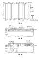
- FIG. 1is a top view of a disk drive with a patterned-media type of magnetic recording disk as described in the prior art.
- FIG. 2is a top view of an enlarged portion of a patterned-media type of magnetic recording disk showing the detailed arrangement of the data islands in one of the bands on the surface of the disk substrate.
- FIG. 3is a side sectional view of one type of a patterned-media disk showing the data islands as elevated, spaced-apart pillars that extend above the disk substrate surface with trenches between the pillars.
- FIG. 4is a schematic view of a patterned-media disk showing a pattern of radial lines in three annular bands, with each radial line meant to represent data islands from all the concentric tracks in the band.
- FIGS. 5A , 5 B and 5 Care views of a small portion of one annular band of the master mold at successive stages of the method of making the master mold according to the present invention.
- FIGS. 6A-6Care side sectional views, at various stages of one embodiment of the method for making the master mold, taken through a plane generally perpendicular to the radial direction.
- FIG. 6Dis a top view of one stage of one embodiment of the method for making the master mold.
- FIGS. 6E-6Gare side sectional views, at various stages of one embodiment of the method for making the master mold, taken through a plane generally perpendicular to the radial direction.
- FIG. 6His a top view of one stage of one embodiment of the method for making the master mold.
- FIG. 6Iis a side sectional view of one stage of one embodiment of the method for making the master mold, taken through a plane generally perpendicular to the radial direction.
- FIGS. 6J-6Lare top views at various stages of one embodiment of the method for making the master mold.
- FIGS. 6M-6Qare side sectional views, at various stages of an alternative embodiment of the method shown in FIGS. 6C-6D , taken through a plane generally perpendicular to the radial direction.
- FIG. 7Ais a side sectional view at one stage of a variation of the method depicted in FIGS. 6A-6L , taken through a plane generally perpendicular to the radial direction.
- FIGS. 7B-7Eare top views at various stages of a variation of the method depicted in FIGS. 6A-6L .
- FIGS. 8A-8Care side sectional views at various stages of another embodiment of the method for making the master mold, taken through a plane generally perpendicular to the radial direction.
- FIG. 1is a top view of a disk drive 100 with a patterned magnetic recording disk 10 as described in the prior art.
- the drive 100has a housing or base 112 that supports an actuator 130 and a drive motor for rotating the magnetic recording disk 10 about its center 13 .
- the actuator 130may be a voice coil motor (VCM) rotary actuator that has a rigid arm 134 and rotates about pivot 132 as shown by arrow 124 .
- a head-suspension assemblyincludes a suspension 121 that has one end attached to the end of actuator arm 134 and a head carrier 122 , such as an air-bearing slider, attached to the other end of suspension 121 .
- the suspension 121permits the head carrier 122 to be maintained very close to the surface of disk 10 .
- a magnetoresistive read head (not shown) and an inductive write head (not shown)are typically formed as an integrated read/write head patterned on the trailing surface of the head carrier 122 , as is well known in the art.
- the patterned magnetic recording disk 10includes a disk substrate 11 and discrete data islands 30 of magnetizable material on the substrate 11 .
- the data islands 30function as discrete magnetic bits for the storage of data and are arranged in radially-spaced circular tracks 118 , with the tracks 118 being grouped into annular bands 119 a , 119 b , 119 c .
- the grouping of the data tracks into annular bandspermits banded recording, wherein the angular spacing of the data islands, and thus the data rate, is different in each band.
- FIG. 1only a few islands 30 and representative tracks 118 are shown in the inner band 119 a and the outer band 119 c .
- the movement of actuator 130allows the read/write head on the trailing end of head carrier 122 to access different data tracks 118 on disk 10 .
- Rotation of the actuator 130 about pivot 132 to cause the read/write head on the trailing end of head carrier 122 to move from near the disk inside diameter (ID) to near the disk outside diameter (OD)will result in the read/write head making an arcuate path across the disk 10 .
- FIG. 2is a top view of an enlarged portion of disk 10 showing the detailed arrangement of the data islands 30 in one of the bands on the surface of disk substrate 11 according to the prior art.
- the islands 30are shown as being circularly shaped and thus have a BAR of 1.
- the islands 30contain magnetizable recording material and are arranged in tracks spaced-apart in the radial or cross-track direction, as shown by tracks 118 a - 118 e .
- the tracksare typically spaced apart by a nearly fixed track pitch or spacing TS.
- the islands 30are roughly equally spaced apart by a nearly fixed along-the-track island pitch or spacing IS, as shown by typical islands 30 a , 30 b , where IS is the spacing between the centers of two adjacent islands in a track.
- the islands 30are also arranged into generally radial lines, as shown by radial lines 129 a , 129 b and 129 c that extend from disk center 13 ( FIG. 1 ). Because FIG. 2 shows only a very small portion of the disk substrate 11 with only a few of the data islands, the pattern of islands 30 appears to be two sets of perpendicular lines.
- tracks 118 a - 118 eare concentric rings centered about the center 13 of disk 10 and the lines 129 a , 129 b , 129 c are not parallel lines, but radial lines extending from the center 13 of disk 10 .
- the angular spacing between adjacent islands as measured from the center 13 of the disk for adjacent islands in lines 129 a and 129 b in a radially inner trackis the same as the angular spacing for adjacent islands in lines 129 a and 129 b in a radially outer track (like track 118 a ).
- the generally radial linesmay be perfectly straight radial lines but are preferably arcs or arcuate-shaped radial lines that replicate the arcuate path of the read/write head on the rotary actuator.
- Such arcuate-shaped radial linesprovide a constant phase position of the data islands as the head sweeps across the data tracks. There is a very small radial offset between the read head and the write head, so that the synchronization field used for writing on a track is actually read from a different track. If the islands between the two tracks are in phase, which is the case if the radial lines are arcuate-shaped, then writing is greatly simplified.
- Patterned-media disks like that shown in FIG. 2may be longitudinal magnetic recording disks, wherein the magnetization directions in the magnetizable recording material are parallel to or in the plane of the recording layer in the islands, or perpendicular magnetic recording disks, wherein the magnetization directions are perpendicular to or out-of-the-plane of the recording layer in the islands.
- the magnetic moment of the regions between the islandsmust be destroyed or substantially reduced to render these spaces essentially nonmagnetic.
- Patterned mediamay be fabricated by any of several known techniques.
- the data islandsare elevated, spaced-apart pillars that extend above the disk substrate surface to define troughs or trenches on the substrate surface between the pillars.
- This type of patterned mediais shown in the sectional view in FIG. 3 .
- the substrate 11 with a pre-etched pattern of pillars 31 and trenches or regions between the pillarscan be produced with relatively low-cost, high volume nanoimprinting process using a master template or mold.
- the magnetic recording layer materialis then deposited over the entire surface of the pre-etched substrate to cover both the ends of the pillars 31 and the trenches between the pillars 31 , resulting in the data islands 30 of magnetic recording layer material and trenches 32 of magnetic recording layer material.
- the trenches 32 of recording layer materialmay be spaced far enough from the read/write head to not adversely affect reading or writing to the recording layer material in islands 30 , or the trenches may be rendered nonmagnetic by “poisoning” with a material like Si.
- This type of patterned mediais described by Moritz et al., “Patterned Media Made From Pre-Etched Wafers: A Promising Route Toward Ultrahigh-Density Magnetic Recording”, IEEE Transactions on Magnetics , Vol. 38, No. 4, July 2002, pp. 1731-1736.
- FIG. 4is a schematic view of patterned-media disk 10 showing a pattern of radial lines in three annular bands 119 a - 119 c .
- Each radial lineis meant to represent data islands from all the concentric tracks in the band.
- the circumferential density of the radial linesis similar in all three bands, with the angular spacing of the lines being adjusted in the bands to have smaller angular spacing in the direction from the disk inside diameter (ID) to outside diameter (OD), so that the circumferential density of the radial lines, and thus the “linear” or along-the-track density of data islands, stays relatively constant over all the bands on the disk.
- IDdisk inside diameter
- ODoutside diameter
- a typical diskis divided into about 20 annular bands, which allows the linear density to remain constant to within a few percent across all bands.
- the radial linesare subdivided (not shown) into very short radial segments or lengths arranged in concentric rings, with each ring being a data track and each radial segment or length being a discrete data island.
- Each annular bandlike band 119 c , has a band ID and a band OD.
- the generally radial linesare more typically generally arcuate lines that replicate the path of the read/write head mounted on the end of the rotary actuator.
- the making of the master template or mold to achieve an ultrahigh density patterned-media diskis a difficult and challenging process.
- the use of electron beam (e-beam) lithography using a Gaussian beam rotary-stage e-beam writeris viewed as a possible method to make the master mold.
- e-beamelectron beam
- a track pitch of about 50 nm and an island pitch of about 12.5 nmwill be required, which would result in a BAR of 4.
- a master mold capable of nanoimprinting patterned-media disks with an island pitch of 12.5 nmis difficult to fabricate due to the limited resolution of e-beam lithography.
- the present inventionrelates to a method for making a master mold that is used in the nanoimprinting process to make patterned-media disks with an island pitch difficult to achieve with the resolution of e-beam lithography, thus enabling both higher areal bit density (1 Tbit/in 2 and higher) and a high BAR (greater than 1).
- the master moldmay be used to directly nanoimprint the disks, but more likely is used to make replica molds which are then used to directly nanoimprint the disks.
- the methoduses conventional or e-beam lithography to form a pattern of generally radial stripes on a substrate, with the stripes being grouped into annular zones or bands.
- a block copolymer materialis deposited on the pattern, resulting in guided self-assembly of the block copolymer into its components to multiply the generally radial stripes into generally radial lines.
- the radial linespreferably have a higher circumferential density than that of the radial stripes.
- Conventional lithographyis then used to form concentric rings over the generally radial lines.
- the master moldAfter etching and resist removal, the master mold has pillars arranged in circular rings, with the rings grouped into annular bands. The spacing of the concentric rings is selected so that following the etching process the master mold has an array of pillars with the desired BAR, which is greater than 1, preferably about 2 or greater.
- the subsequently nanoimprinted patterned-media diskscan have both a high BAR (greater than 1 and preferably about 2 or greater) and an ultra-high areal density.
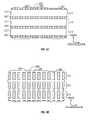
- FIGS. 5A-5Cshow a small portion of one annular band of the master mold with the radial or cross-track direction being vertical and the circumferential or along-the-track direction being horizontal.
- the first stepis to create a pattern of generally radial stripes 204 on substrate 200 at a density achievable by conventional e-beam or other lithography.
- FIG. 5Bthe circumferential density of radial stripes 204 is multiplied by two as a result of guided self-assembly of block copolymer material into its components, resulting in generally radial lines 212 representing one of the block copolymer components.
- the radial lines 212are used as an etch mask to etch radial lines in the substrate and a second conventional e-beam or other lithography step is performed to cut the radial lines of substrate material into circumferential segments 213 of pillars 228 .
- the pillars 228correspond to the data islands and the segments 213 correspond to the data tracks on the disks that will be nanoimprinted.
- the pillars 228have a circumferential pitch difficult to achieve with the resolution of e-beam lithography.
- the array of pillars 228has a BAR greater than 1, preferably about 2 or greater.
- a self-assembling block copolymertypically contains two or more different polymeric block components, for example components A and B, that are immiscible with one another. Under suitable conditions, the two or more immiscible polymeric block components separate into two or more different phases or microdomains on a nanometer scale and thereby form ordered patterns of isolated nano-sized structural units.
- suitable block copolymersthat can be used for forming the self-assembled periodic patterns include, but are not limited to: poly(styrene-block-methyl methacrylate) (PS-b-PMMA), poly(ethylene oxide-block-isoprene) (PEO-b-PI), poly(ethylene oxide-block-butadiene) (PEO-b-PBD), poly(ethylene oxide-block-styrene) (PEO-b-PS), poly(ethylene oxide-block-methylmethacrylate) (PEO-b-PMMA), poly(ethyleneoxide-block-ethylethylene) (PEO-b-PEE), poly(styrene-block-vinylpyridine) (PS-b-PVP), poly(styrene-block-isoprene) (PS-b-PI), poly(styrene-block-butadiene) (PS-b-PBD), poly(styrene-block-ferrocenyldimethylsilane)
- the specific self-assembled periodic patterns formed by the block copolymerare determined by the molecular volume ratio between the first and second polymeric block components A and B.
- the ratio of the molecular volume of the second polymeric block component B over the molecular volume of the first polymeric block component Ais less than about 80:20 but greater than about 60:40, the block copolymer will form an ordered array of cylinders composed of the first polymeric block component A in a matrix composed of the second polymeric block component B.
- the block copolymerwill form alternating lamellae composed of the first and second polymeric block components A and B.
- the un-removed componentis to be used as an etch mask for forming the generally radial lines, as shown in FIG. 5B , so ordered arrays of alternating lamellae and alternating cylinders are of interest.
- the periodicity or bulk period (L 0 ) of the repeating structural units in the periodic patternis determined by intrinsic polymeric properties such as the degree of polymerization N and the Flory-Huggins interaction parameter ⁇ .
- L 0scales with the degree of polymerization N, which in turn correlates with the molecular weight M. Therefore, by adjusting the total molecular weight of the block copolymer of the present invention, the bulk period (L 0 ) of the repeating structural units can be selected.
- the block copolymeris first dissolved in a suitable solvent system to form a block copolymer solution, which is then applied onto the substrate surface to form a thin block copolymer layer, followed by annealing of the thin block copolymer layer, which causes phase separation between the different polymeric block components contained in the block copolymer.
- the solvent system used for dissolving the block copolymer and forming the block copolymer solutionmay comprise any suitable solvent, including, but not limited to: toluene, propylene glycol monomethyl ether acetate (PGMEA), propylene glycol monomethyl ether (PGME), and acetone.
- the block copolymer solutioncan be applied to the substrate surface by any suitable techniques, including, but not limited to: spin casting, coating, spraying, ink coating, dip coating, etc.
- the block copolymer solutionis spin cast onto the substrate surface to form a thin block copolymer layer.
- the entire substrateis annealed to effectuate microphase segregation of the different block components contained by the block copolymer, thereby forming the periodic patterns with repeating structural units.
- the block copolymer films in the above-described techniquesself-assemble without any direction or guidance. This undirected self-assembly results in patterns with defects so it is not practical for applications that require long-range ordering, such as for making annular bands of radial lines on a master mold for nanoimprinting patterned-media disks.
- Lithographically patterned surfaceshave been proposed to guide or direct the self-assembly of block copolymer domains.
- One approachuses interferometric lithography to achieve ordering of the domains with registration of the underlying chemical contrast pattern on the substrate. Lamellar and cylindrical domains may be formed on a substrate by this technique, as described in U.S. Pat. No. 6,746,825.
- interferometric lithographycannot be used to make annular bands of radial lines.
- US 2006/0134556 A1describes techniques for creating a chemical contrast pattern to guide the self-assembly of block copolymers to form aperiodic patterns.
- the periodicity of the underlying chemical contrast patternmatches the bulk period L 0 of the block copolymer.
- L 0is about 40 nm
- the lithographically-patterned substrate used to guide the self-assemblyalso has a period of about 40 nm, which can be achieved by conventional or e-beam lithography.
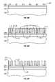
- FIGS. 6A-6LA first embodiment of the method of this invention for making the master mold will now be explained with respect to FIGS. 6A-6L .
- FIGS. 6A-6C , 6 E- 6 G and 6 Iare side sectional views, at various stages of the fabrication method, taken through a plane generally perpendicular to the radial direction, and FIGS. 6D , 6 H and 6 J- 6 L are top views at various stages of the method.
- the master mold substratecomprises a base 200 , which may be formed of Si or SiO 2 , a first substrate layer 202 , which is preferably about a 10 nm thick amorphous carbon layer, and second substrate layer 204 , which is preferably about a 5 nm thick layer of germanium (Ge).
- a base 200which may be formed of Si or SiO 2
- first substrate layer 202which is preferably about a 10 nm thick amorphous carbon layer
- second substrate layer 204which is preferably about a 5 nm thick layer of germanium (Ge).
- germaniumgermanium
- Other combinations of materialscan be used, as long as materials and etchants can be chosen to allow selective removal of the materials (without disturbing the others) as needed for the described processes that follow.
- materials for the first layer 202include Al, carbon, Cr, Si 3 N 4 , and variety of other materials that can withstand a reactive-ion-etch (RIE) process used to etch the quartz substrate.
- RIEreactive-i
- the choice of materials for layer 202is further broadened.
- one of the following materials(but different from the material of the first layer 202 ) may be used: Cr, Al, SiO 2 , Si, Ge, carbon, Si 3 N 4 , W, or a variety of other materials, as long as they can withstand the RIE used to etch the first layer.
- the Ge layer 204will have a native Ge-oxide film on its surface.
- a neutral layer 205 of a material that does not show a strong wetting affinity by one of the polymer blocks over the otheris deposited onto the Ge layer 204 .
- the neutral layercan be, but is not restricted to, a functionalized polymer brush, a cross-linkable polymer, a functionalized polymer “A” or “B” or a functionalized random copolymer “A-r-B” or a blend of “A” and “B”, where “A” and “B” are the constituent block materials of the block copolymer.
- the functional groupmay be, for example, a hydroxyl group.
- the neutral layer 205is a hydroxyl-terminated polystyrene brush of lower molecular weight than the block copolymer used.
- the brush materialis spin-coated on Ge layer 204 to a thickness of about 1-10 nm (below 6 nm is preferred).
- the purpose of the neutral layeris to tune the surface energy adequately to promote the desired domain orientation (perpendicular lamellae or parallel cylinders) and to provide the adequate wetting conditions for density multiplication.
- a resist layerhas been deposited on brush layer 205 and patterned into generally radial bars 210 of resist.
- the resist layeris patterned by e-beam and developed to form the pattern of radial bars 210 separated by radial spaces 211 that expose portions of brush layer 205 .
- the e-beam toolpatterns the resist layer so that the radial spaces 211 have a circumferential spacing that is approximately an integer multiple of L 0 (i.e., nL 0 ), the known bulk period for the selected block copolymer that will be subsequently deposited.
- nis 2.
- the circumferential width of each radial space 211is selected to be approximately 0.5 L 0 .
- the structureis etched, by a process of oxygen plasma reactive ion etching (O 2 RIE), to remove portions of brush layer 205 in the radial spaces 211 , which exposes portions of Ge layer as generally radial stripes 204 .
- O 2 RIEoxygen plasma reactive ion etching
- the chemical structure of the exposed portions of brush layer 205 in the radial spaces 211can be altered so that they have a preferred affinity for one of the copolymers.
- FIG. 6Dwhich is a top view, the resist 210 is removed, leaving on the substrate a pattern of generally radial bars 205 of polymer brush material separated by generally radial stripes 204 of Ge.
- the generally radial stripes 204have a circumferential width of 0.5 L 0 and a circumferential pitch of 2 L 0 .
- the structure in FIG. 6Dcorresponds generally to the step shown in FIG. 5A . Because FIG. 6D is only a very small portion of the master mold, the stripes 204 appear as parallel stripes. However, the stripes 204 are arranged generally radially, as depicted in FIG. 4 .
- the stripes 204may be perfectly straight radial stripes but are preferably arcs or arcuate-shaped radial stripes that replicate the arcuate path of the read/write head on the rotary actuator.
- a layer 220 of block copolymer materialis deposited over the radial bars 205 of brush material and the radial stripes 204 of Ge layer (or chemically altered brush) in the radial spaces 211 .
- the preferred block copolymer materialis the diblock copolymer polystyrene-block-polymethylmethacrylate (PS-b-PMMA) with L 0 between about 8 nm and 25 nm and is deposited by spin coating to a thickness of about 0.5 L 0 to 3 L 0 .
- the block copolymer layerhas been annealed, which results in phase separation between the different components contained in the block copolymer.
- the B componentPMMA
- the B componenthas an affinity for the oxide surface of the Ge stripes or for the polar groups of the chemically altered brush 204 and thus form as generally radial lines 215 on top of the radial Ge stripes 204 .
- the circumferential width of the Ge stripes 204is approximately 0.5 L 0
- the A component (PS)form in adjacent radial lines 212 on the radial bars 205 of polymer brush material.
- the B componentAs a result of the self-assembly of the A and B components this causes the B component to also form as generally radial lines 215 on the centers of each radial bar 205 of polymer brush material.
- the generally radial Ge stripes 204(or chemically altered brush) thus guide the self-assembly of the PS and PMMA components to form the alternating radial lines 212 , 215 in the structure as shown in FIG. 6F .
- the substrate pattern of radial stripes 204guides the alternating lines 212 , 215 to form as radial lines, which means that that L 0 cannot be constant over the entire radial length.
- a pattern of alternating radial lines 212 , 215can be accomplished without any significant defects if the variation from L 0 does not exceed approximately 10 percent.
- the circumferential spacing of the radial stripes 204 at the band IDshould not be less than about 0.9nL 0 and the circumferential spacing of the radial stripes 204 at the band OD should not be greater than about 1.1nL 0 .
- FIG. 6Gis a top view of FIG. 6G and shows the generally radial A-component lines 212 with a circumferential spacing L 0 .
- FIG. 6Hcorresponds generally to the step shown in FIG. 5B , where the circumferential density of radial lines 212 has been doubled from the circumferential density of radial stripes 204 in FIG. 5A .
- the Ge layer 204has been etched, using the PS radial lines 212 as an etch mask, by a fluorine-based reactive-ion-etch (RIE) process.
- RIEreactive-ion-etch
- the PS material in radial lines 212 and the underlying polymer brush layer 205has been removed by a dry etch process (O 2 RIE).
- the Ge lines 208have the same circumferential spacing L 0 as the radial lines 212 of PS material in FIG. 6H .
- FIG. 6Jwhich is a top view
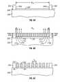
- the structure of FIG. 6Iis coated with a layer of e-beam resist 217 .
- the resist 217is exposed in a rotary-stage e-beam tool to expose narrow concentric boundary regions 207 that correspond to the boundaries between the tracks of the patterned-media disks to be nanoimprinted.
- the resist 217may be a positive e-beam resist like poly methyl methacrylate (PMMA) or ZEP520 from Zeon Chemicals, L.P.
- a fluorine-based RIEis used to etch the exposed Ge in the boundary regions 207 . Then the resist 217 is removed in a wet etch process, like hot N-methyl pyrrolidone (NMP), or a dry etch process, like oxygen RIE. This leaves Ge pillars 226 on carbon layer 202 .
- FIG. 6Lan oxygen RIE is used to etch the carbon layer 202 from the substrate 200 in the regions between the Ge pillars 226 , using the Ge pillars 226 as an etch mask.
- the Ge pillars 226are then removed by a fluorine RIE process, leaving carbon pillars 228 on substrate base 200 .
- the resulting structure in FIG. 6Mcorresponds generally to the step shown in FIG. 5C .
- the carbon pillars 228have a IAR of greater than 1, preferably about 2 or greater.
- FIG. 6Lwhich began as a substrate of base 200 with carbon layer 202 and Ge layer 204 , has now been etched so that a portion of the substrate remains as the topographic pattern in the form of carbon pillars 228 .
- the structure of FIG. 6Lcan function as the master mold with the carbon pillars 228 functioning as the topographic pattern for nanoimprinting the replica molds.
- the carbon pillars 228 in FIG. 6Lcan function as an etch mask for an additional etching step to etch the underlying substrate base 200 using a fluorine RIE process. After etching and removal of the carbon pillars 228 in this alternative approach, the result would be a master mold wherein the pillars are formed of the same material as the substrate base 200 .
- the pillars 228have a circumferential pitch of about 15 nm and a circumferential width of about 8 nm and a radial length of about 25 nm with a radial pitch of about 30 nm, resulting in a BAR of greater than about 2.
- the 15 nm pillar spacing or pitch in the circumferential directioncorresponds approximately to L 0 and is half of that used in the e-beam lithography step which defined the radial stripes 204 in FIG. 6D .
- This arraymay be used as a master mold for nanoimprinting patterned-media disks with a density of about 1.4 Gigabit/in 2 .
- FIGS. 6M-6QAn alternative to the steps shown in FIGS. 6C-6F will also generate the necessary pattern on the substrate. This is shown in FIGS. 6M-6Q .
- the structure in FIG. 6Bis used as the starting point.
- a material 250 with a wetting affinity for one of the two polymer blocks, such as SiO 2is deposited in the radial spaces 211 to a thickness of about 1 nm.
- the radial bars 210 of resistare removed, leaving on the substrate a pattern of generally radial stripes 250 of SiO 2 separated by generally radial spaces 205 of polymer brush material.
- the generally radial stripes 250have a circumferential width of 0.5 L 0 and a circumferential pitch of 2 L 0 . Because FIG. 6N is only a very small portion of the master mold, the stripes 250 appear as parallel stripes. However, the stripes 250 are arranged generally radially, as depicted in FIG. 4 . The stripes 250 may be perfectly straight radial stripes but are preferably arcs or arcuate-shaped radial stripes that replicate the arcuate path of the read/write head on the rotary actuator.
- a layer of block copolymer materialis deposited over the radial stripes 250 of SiO 2 and the radial spaces 205 of polymer brush material.
- the preferred block copolymer materialis the diblock copolymer polystyrene-block-polymethylmethacrylate (PS-b-PMMA) with L 0 between about 8 nm and 25 nm and is deposited by spin coating to a thickness of about 0.5 L 0 to 3 L 0 .
- the block copolymer layerhas been annealed, which results in phase separation between the different components contained in the block copolymer.
- the B component (PMMA)has an affinity for the oxide surface of the radial SiO 2 stripes 250 and thus form as generally radial lines 215 on top of the radial SiO 2 stripes 250 .
- the A component (PS)form in adjacent radial lines 212 in the radial spaces 205 of polymer brush material.
- thiscauses the B component to also form as generally radial lines 215 in the centers of each radial space 205 of polymer brush material.
- the generally radial SiO 2 stripes 250thus guide the self-assembly of the PS and PMMA components to form the alternating radial lines 212 , 215 in the structure as shown in FIG. 6O .
- the B component (PMMA)is selectively removed by a wet etch (acetic acid, iso-propyl alcohol (IPA) or other selective solvent) or dry etch process (O 2 RIE), leaving generally radial lines 212 of the A component (PS) and the generally radial SiO 2 stripes 250 .
- a wet etchacetic acid, iso-propyl alcohol (IPA) or other selective solvent
- O 2 RIEdry etch process
- the remaining exposed brush layer 205 in the spaces between radial lines 212is then removed by O 2 RIE, leaving generally radial lines 212 of the A component (PS) and the generally radial lines 204 of Ge. At this point the structure is identical to that shown in FIG. 6G and the process can continue as described above.
- FIGS. 7A-7EA variation of the embodiment of the methods shown in FIGS. 6A-6O is shown in FIGS. 7A-7E , wherein FIG. 7A is a side sectional view taken through a plane generally perpendicular to the radial direction, and FIGS. 7B-7E are top views at various stages of the method.
- the master mold substrateis base 200 which is a Si substrate with a native oxide layer.
- FIG. 7Acorresponds to the stage of the method shown by FIG. 6G .
- the B component (PMMA)has been dissolved by a wet etch or dry etch process, leaving generally radial lines 212 of the A component (PS).
- FIG. 7Bis a top view of FIG.
- FIG. 7Ashows the generally radial lines 212 with a circumferential spacing L 0 .
- FIG. 7Acorresponds generally to the step shown in FIG. 5B , where the circumferential density of radial lines 212 has been doubled from the circumferential density of radial stripes 204 in FIG. 5A .
- FIG. 7Cwhich is a top view
- the structure of FIGS. 7A-7Bis coated with a layer of e-beam resist 217 .
- the resist 217is exposed in a rotary-stage e-beam tool to expose narrow concentric boundary regions 207 that correspond to the boundaries between the tracks of the patterned-media disks to be nanoimprinted.
- the resist 217may be a positive e-beam resist like PMMA or ZEP520.
- the PS (block copolymer component A) in the exposed portions of radial lines 212 in the boundary regions 207is removed by a O 2 RIE process.
- the resist 217is removed in a wet etch process, like hot NMP. This leaves pillars 226 ′ of PS on substrate 200 .
- FIG. 7Ea dry etch process is used to etch the substrate 200 in the regions between the PS pillars 226 ′, using the PS pillars 226 ′ as an etch mask.
- the PS pillars 226 ′are then removed by a O 2 RIE process, leaving pillars 228 ′ of substrate material on substrate 200 .
- the resulting structure in FIG. 7Ecorresponds generally to the step shown in FIG. 5C .
- FIG. 7Ewhich began as a substrate of base 200 , has now been etched so that a portion of the substrate remains as the topographic pattern in the form of pillars 218 ′.
- the structure of FIG. 7Ecan function as the master mold with the pillars 218 ′ functioning as the topographic pattern for nanoimprinting the replica molds.
- FIGS. 8A-CAnother embodiment of the method for making the master mold is shown in FIGS. 8A-C .
- the structure shown in FIG. 8Awhich is a side sectional view taken through a plane generally perpendicular to the radial direction, is made by starting with a substrate 300 , which may be formed of Si or SiO 2 . Then a layer 305 of neutral polymer brush material is deposited over the entire surface of substrate 300 . A layer of resist is then deposited over brush layer 305 and patterned with conventional optical or e-beam lithography. After exposure and development a pattern of generally radial stripes are formed that expose the underlying brush layer 305 .
- the bottom of the trenchis formed of the neutral brush layer 305 and the walls 304 a of radial stripes 304 have a native oxide surface.
- a layer of block copolymer materialhas been deposited between the radial stripes 304 and onto neutral brush layer 305 .
- the preferred block copolymer materialis the diblock copolymer polystyrene-block-polymethylmethacrylate (PS-b-PMMA) with L 0 between about 8 nm and 25 nm and is deposited by spin coating to a thickness of about 0.5 L 0 to 3 L 0 .
- PS-b-PMMAdiblock copolymer polystyrene-block-polymethylmethacrylate
- the block copolymeris then annealed, which results in phase separation between the different components contained in the block copolymer.
- the B componentPMMA
- the B componentis formed on the walls 304 a of the radial stripes 304 as radial lines 215 a and because the circumferential width between the walls 304 a of radial stripes 304 is an integer multiple of L 0 (9 L 0 in the example of FIG. 8B ), the A and B components between radial B-component lines 215 a are forced to self-assemble in alternating radial lines 212 , 215 , each with a circumferential width of approximately 0.5 L 0 .
- the circumferential width of B-component radial lines 215 ais approximately 0.25 L 0 .
- the generally radial stripes 304which are spaced apart to define a trench with circumferential width of approximately nL 0 , thus guide the self-assembly of the PS and PMMA components to form the alternating radial lines 212 , 215 in the structure as shown in FIG. 8B .
- the pattern of radial stripes 304 on the substrate 300guides the alternating lines 212 , 215 to form as radial lines, which means that L 0 cannot be constant over the entire radial length of the band.
- the pattern of alternating radial lines 212 , 215can be accomplished without any significant defects if the variation from L 0 does not exceed approximately 10 percent.
- the circumferential width of the trench at the band IDshould not be less than about 0.9 nL 0 and the circumferential width of the trench at the band OD should not be greater than about 1.1nL 0 .
- FIG. 8Cthe B component (PMMA), which formed the radial lines 215 a and 215 in FIG. 8B , have been dissolved by a wet etch process (acetic acid, IPA or other selective solvent) or by a dry etch process (O 2 RIE), leaving generally radial lines 212 of the A component (PS).
- a wet etch processacetic acid, IPA or other selective solvent
- O 2 RIEdry etch process
- patterned-media disks nanoimprinted by the master mold made by the method shown in FIGS. 8A-8Cwill have missing bits at predictable regular intervals in each track as a result of the radials stripes 304 which are needed to define the circumferential trenches.
- a relatively constant bit spacingis desired for accurate write synchronization and readback detection because if the spacing between the bits is not constant, phase errors may occur. If the phase error due to the missing bits becomes more than a few percent of the bit spacing, the errors may be unacceptable.
- a modification to the method of FIGS. 8A-8Cwill avoid any phase errors due to the radial stripes 304 .
- the circumferential width of the radial stripes 304is selected to be 0.5 L 0 .
- Each wall surface 304 ais then coated with a PMMA brush of thickness about 0.25 L 0 , so that the spacing between the coated walls is 9 L 0 .
- the block copolymeris applied and the process is the same as above.
- the radial stripes 304substitute for one PS stripe while guiding the self-assembly of the block copolymer.
- the PMMA brush on the walls 304 acompensate for the missing material.
- the two block copolymer componentsare depicted as self-assembling into alternating lamellae, as shown, for example, by alternating radial lines 212 , 215 in FIG. 6F .
- the molecular weight ratio of the A to B componentsshould be between about 40:60 and 60:40, preferably close to 50:50.
- the A component (PS)to form as radially-aligned cylinders within a matrix of the B component (PMMA).
- the molecular weight ratio of component B over component Ashould be less than about 80:20 but greater than about 60:40, preferably close to 70:30.
- the master mold shown in FIGS. 6L and 7Eis a pillar-type master mold that can be used to make replica molds.
- the replica moldswill thus have hole patterns corresponding to the pillar pattern of the master mold.
- the master moldmay alternatively be a hole-type of master mold that can be used to directly nanoimprint the disks.
Landscapes
- Manufacturing Of Magnetic Record Carriers (AREA)
- Exposure Of Semiconductors, Excluding Electron Or Ion Beam Exposure (AREA)
Abstract
Description
- 1. Field of the Invention
- This invention relates generally to patterned-media magnetic recording disks, wherein each data bit is stored in a magnetically isolated data island on the disk, and more particularly to a method for making a master mold to be used for nanoimprinting the patterned-media disks.
- 2. Description of the Related Art
- Magnetic recording hard disk drives with patterned magnetic recording media have been proposed to increase data density. In patterned media, the magnetic recording layer on the disk is patterned into small isolated data islands arranged in concentric data tracks. To produce the required magnetic isolation of the patterned data islands, the magnetic moment of spaces between the islands must be destroyed or substantially reduced to render these spaces essentially nonmagnetic. In one type of patterned media, the data islands are elevated regions or pillars that extend above “trenches” and magnetic material covers both the pillars and the trenches, with the magnetic material in the trenches being rendered nonmagnetic, typically by “poisoning” with a material like silicon (Si). Patterned-media disks may be longitudinal magnetic recording disks, wherein the magnetization directions are parallel to or in the plane of the recording layer, or perpendicular magnetic recording disks, wherein the magnetization directions are perpendicular to or out-of-the-plane of the recording layer.
- One proposed method for fabricating patterned-media disks is by nanoimprinting with a template or mold, sometimes also called a “stamper”, that has a topographic surface pattern. In this method the magnetic recording disk substrate with a polymer film on its surface is pressed against the mold. The polymer film receives the reverse image of the mold pattern and then becomes a mask for subsequent etching of the disk substrate to form the pillars on the disk. The magnetic layer and other layers needed for the magnetic recording disk are then deposited onto the etched disk substrate and the tops of the pillars to form the patterned-media disk. The mold may be a master mold for directly imprinting the disks. However, the more likely approach is to fabricate a master mold with a pattern of pillars corresponding to the pattern of pillars desired for the disks and to use this master mold to fabricate replica molds. The replica molds will thus have a pattern of holes corresponding to the pattern of pillars on the master mold. The replica molds are then used to directly imprint the disks. Nanoimprinting of patterned media is described by Bandic et al., “Patterned magnetic media: impact of nanoscale patterning on hard disk drives”,Solid State Technology S7+ Suppl. S, SEP2006; and by Terris et al., “TOPICAL REVIEW: Nanofabricated and self-assembled magnetic structures as data storage media”,J. Phys. D: Appl. Phys.38 (2005) R199-R222.
- In patterned media, there are two opposing requirements relating to the bit-aspect-ratio (BAR) of the pattern or array of discrete data islands arranged in concentric tracks. The BAR is the ratio of track spacing or pitch in the radial or cross-track direction to the island spacing or pitch in the circumferential or along-the-track direction, which is the same as the ratio of linear island density in bits per inch (BPI) in the along-the-track direction to the track density in tracks per inch (TPI) in the cross-track direction. The BAR is also equal to the ratio of the radial dimension of the bit cell to the circumferential dimension of the bit cell, where the data island is located within the bit cell. The bit cell includes not only the magnetic data island but also one-half of the nonmagnetic space between the data island and its immediately adjacent data islands. The data islands have an island aspect ratio (IAR) or radial length to circumferential that is generally close to the BAR. The first requirement is that to minimize the resolution requirement for fabricating the islands, it is preferable that the array of islands have a low BAR (about 1). The second requirement is that to allow for a wider write head pole, which is necessary for achieving a high write field to allow the use of high coercivity media for thermal stability, it is preferable that the array of islands have a higher BAR (about 2 or greater). Also, the transition from disk drives with conventional continuous media to disk drives with patterned media is simplified if the BAR is high because in conventional disk drives the BAR is between about 5 to 10. Other benefits of higher BAR include lower track density, which simplifies the head-positioning servo requirements, and a higher data rate.
- The making of the master template or mold is a difficult and challenging process. The use of electron beam (e-beam) lithography using a Gaussian beam rotary-stage e-beam writer is viewed as a possible method to make a master mold capable of nanoimprinting patterned-media disks with a BAR of about 1 with a track pitch (island-to-island spacing in the radial or cross-track direction) of about 35 nm, and an island pitch (island-to-island spacing in the circumferential or along-the-track direction) of about 35 nm. If the data islands have a radial length and circumferential width each of about 20 nm for an IAR of 1, then these dimensions generally limit the areal bit density of patterned-media disks to about 500 Gbit/in2. To achieve patterned-media disks with both an ultra-high areal bit density (around 1 Terabits/in2) and a higher BAR, a track pitch of 50 nm and an island pitch of about 12.5 nm will be required, which would result in a BAR of 4. However, a master mold capable of nanoimprinting patterned-media disks with an island pitch of 12.5 nm is not achievable with the resolution of e-beam lithography.
- What is needed is a master mold and a method for making it that can result in patterned-media magnetic recording disks with both the required high areal bit density and higher BAR (about 2 or greater).
- The invention is a method for making a master mold to be used for nanoimprinting patterned-media magnetic recording disks with a BAR greater than 1, preferably about 2 or greater. The method uses conventional optical or e-beam lithography to form a pattern of generally radial stripes on a substrate, with the stripes being grouped into annular zones or bands. A block copolymer material is deposited on the pattern, resulting in guided self-assembly of the block copolymer into its components to multiply the generally radial stripes into generally radial lines of alternating block copolymer components. The radial lines of one of the components are removed and the radial lines of the remaining component are used as an etch mask to etch the substrate. Conventional lithography is used to form concentric rings over the generally radial lines. After etching and resist removal, the master mold has pillars arranged in circular rings, with the rings grouped into annular bands. The spacing of the concentric rings is selected so that following the etching process the master mold has an array of pillars with the desired BAR, which is greater than 1, preferably about 2 or greater. The master mold may be used to directly nanoimprint the disks, but more likely is used to make replica molds which are then used to directly nanoimprint the disks.
- The block copolymer may be a diblock copolymer of A and B components having the structure (A-b-B), such as polystyrene-block-polymethylmethacrylate (PS-b-PMMA). The ratio of the molecular weight of the A component to the molecular weight of the B component is selected so that the radial lines of the A component are formed either as cylinders in a matrix of the B component or as alternating lamellae separated by alternating lamellae of the B component. The two or more immiscible polymeric block components microphase separate into two or more different microdomains on a nanometer scale and thereby form ordered patterns of isolated nano-sized structural units having a periodicity or bulk period (L0) of the repeating A-B domain units. The block copolymer is selected to have L0in the range of between about 8 nm and 25 nm, which corresponds to the circumferential spacing of the A-component radial lines to be used as the etch mask. However, the generally radial stripes used to guide the self-assembly of the block copolymer into its A and B components have a circumferential spacing of approximately nL0, where n is an integer greater than or equal to 2.
- For a fuller understanding of the nature and advantages of the present invention, reference should be made to the following detailed description taken together with the accompanying figures.
FIG. 1 is a top view of a disk drive with a patterned-media type of magnetic recording disk as described in the prior art.FIG. 2 is a top view of an enlarged portion of a patterned-media type of magnetic recording disk showing the detailed arrangement of the data islands in one of the bands on the surface of the disk substrate.FIG. 3 is a side sectional view of one type of a patterned-media disk showing the data islands as elevated, spaced-apart pillars that extend above the disk substrate surface with trenches between the pillars.FIG. 4 is a schematic view of a patterned-media disk showing a pattern of radial lines in three annular bands, with each radial line meant to represent data islands from all the concentric tracks in the band.FIGS. 5A ,5B and5C are views of a small portion of one annular band of the master mold at successive stages of the method of making the master mold according to the present invention.FIGS. 6A-6C are side sectional views, at various stages of one embodiment of the method for making the master mold, taken through a plane generally perpendicular to the radial direction.FIG. 6D is a top view of one stage of one embodiment of the method for making the master mold.FIGS. 6E-6G are side sectional views, at various stages of one embodiment of the method for making the master mold, taken through a plane generally perpendicular to the radial direction.FIG. 6H is a top view of one stage of one embodiment of the method for making the master mold.FIG. 6I is a side sectional view of one stage of one embodiment of the method for making the master mold, taken through a plane generally perpendicular to the radial direction.FIGS. 6J-6L are top views at various stages of one embodiment of the method for making the master mold.FIGS. 6M-6Q are side sectional views, at various stages of an alternative embodiment of the method shown inFIGS. 6C-6D , taken through a plane generally perpendicular to the radial direction.FIG. 7A is a side sectional view at one stage of a variation of the method depicted inFIGS. 6A-6L , taken through a plane generally perpendicular to the radial direction.FIGS. 7B-7E are top views at various stages of a variation of the method depicted inFIGS. 6A-6L .FIGS. 8A-8C are side sectional views at various stages of another embodiment of the method for making the master mold, taken through a plane generally perpendicular to the radial direction.FIG. 1 is a top view of adisk drive 100 with a patternedmagnetic recording disk 10 as described in the prior art. Thedrive 100 has a housing orbase 112 that supports anactuator 130 and a drive motor for rotating themagnetic recording disk 10 about itscenter 13. Theactuator 130 may be a voice coil motor (VCM) rotary actuator that has arigid arm 134 and rotates aboutpivot 132 as shown byarrow 124. A head-suspension assembly includes asuspension 121 that has one end attached to the end ofactuator arm 134 and ahead carrier 122, such as an air-bearing slider, attached to the other end ofsuspension 121. Thesuspension 121 permits thehead carrier 122 to be maintained very close to the surface ofdisk 10. A magnetoresistive read head (not shown) and an inductive write head (not shown) are typically formed as an integrated read/write head patterned on the trailing surface of thehead carrier 122, as is well known in the art.- The patterned
magnetic recording disk 10 includes adisk substrate 11 anddiscrete data islands 30 of magnetizable material on thesubstrate 11. Thedata islands 30 function as discrete magnetic bits for the storage of data and are arranged in radially-spacedcircular tracks 118, with thetracks 118 being grouped intoannular bands FIG. 1 , only afew islands 30 andrepresentative tracks 118 are shown in theinner band 119aand theouter band 119c. As thedisk 10 rotates about itscenter 13 in the direction ofarrow 20, the movement ofactuator 130 allows the read/write head on the trailing end ofhead carrier 122 to accessdifferent data tracks 118 ondisk 10. Rotation of theactuator 130 aboutpivot 132 to cause the read/write head on the trailing end ofhead carrier 122 to move from near the disk inside diameter (ID) to near the disk outside diameter (OD) will result in the read/write head making an arcuate path across thedisk 10. FIG. 2 is a top view of an enlarged portion ofdisk 10 showing the detailed arrangement of thedata islands 30 in one of the bands on the surface ofdisk substrate 11 according to the prior art. Theislands 30 are shown as being circularly shaped and thus have a BAR of 1. Theislands 30 contain magnetizable recording material and are arranged in tracks spaced-apart in the radial or cross-track direction, as shown bytracks 118a-118e. The tracks are typically spaced apart by a nearly fixed track pitch or spacing TS. Within eachtrack 118a-118e, theislands 30 are roughly equally spaced apart by a nearly fixed along-the-track island pitch or spacing IS, as shown bytypical islands islands 30 are also arranged into generally radial lines, as shown byradial lines FIG. 1 ). BecauseFIG. 2 shows only a very small portion of thedisk substrate 11 with only a few of the data islands, the pattern ofislands 30 appears to be two sets of perpendicular lines. However,tracks 118a-118eare concentric rings centered about thecenter 13 ofdisk 10 and thelines center 13 ofdisk 10. Thus the angular spacing between adjacent islands as measured from thecenter 13 of the disk for adjacent islands inlines track 118e) is the same as the angular spacing for adjacent islands inlines track 118a).- The generally radial lines (like
lines - Patterned-media disks like that shown in
FIG. 2 may be longitudinal magnetic recording disks, wherein the magnetization directions in the magnetizable recording material are parallel to or in the plane of the recording layer in the islands, or perpendicular magnetic recording disks, wherein the magnetization directions are perpendicular to or out-of-the-plane of the recording layer in the islands. To produce the required magnetic isolation of the patterned data islands, the magnetic moment of the regions between the islands must be destroyed or substantially reduced to render these spaces essentially nonmagnetic. Patterned media may be fabricated by any of several known techniques. In one type of patterned media, the data islands are elevated, spaced-apart pillars that extend above the disk substrate surface to define troughs or trenches on the substrate surface between the pillars. This type of patterned media is shown in the sectional view inFIG. 3 . In this type of patterned media thesubstrate 11 with a pre-etched pattern ofpillars 31 and trenches or regions between the pillars can be produced with relatively low-cost, high volume nanoimprinting process using a master template or mold. The magnetic recording layer material is then deposited over the entire surface of the pre-etched substrate to cover both the ends of thepillars 31 and the trenches between thepillars 31, resulting in thedata islands 30 of magnetic recording layer material andtrenches 32 of magnetic recording layer material. Thetrenches 32 of recording layer material may be spaced far enough from the read/write head to not adversely affect reading or writing to the recording layer material inislands 30, or the trenches may be rendered nonmagnetic by “poisoning” with a material like Si. This type of patterned media is described by Moritz et al., “Patterned Media Made From Pre-Etched Wafers: A Promising Route Toward Ultrahigh-Density Magnetic Recording”,IEEE Transactions on Magnetics, Vol. 38, No. 4, July 2002, pp. 1731-1736. FIG. 4 is a schematic view of patterned-media disk 10 showing a pattern of radial lines in three annular bands119a-119c. Each radial line is meant to represent data islands from all the concentric tracks in the band. The circumferential density of the radial lines is similar in all three bands, with the angular spacing of the lines being adjusted in the bands to have smaller angular spacing in the direction from the disk inside diameter (ID) to outside diameter (OD), so that the circumferential density of the radial lines, and thus the “linear” or along-the-track density of data islands, stays relatively constant over all the bands on the disk. In actuality, a typical disk is divided into about 20 annular bands, which allows the linear density to remain constant to within a few percent across all bands. Within each band, the radial lines are subdivided (not shown) into very short radial segments or lengths arranged in concentric rings, with each ring being a data track and each radial segment or length being a discrete data island. Each annular band, likeband 119c, has a band ID and a band OD. Also, in actuality the generally radial lines are more typically generally arcuate lines that replicate the path of the read/write head mounted on the end of the rotary actuator.- The making of the master template or mold to achieve an ultrahigh density patterned-media disk is a difficult and challenging process. The use of electron beam (e-beam) lithography using a Gaussian beam rotary-stage e-beam writer is viewed as a possible method to make the master mold. However, to achieve patterned-media disks with both higher areal bit density (around 1 Tbit/in2) and a higher BAR, a track pitch of about 50 nm and an island pitch of about 12.5 nm will be required, which would result in a BAR of 4. A master mold capable of nanoimprinting patterned-media disks with an island pitch of 12.5 nm is difficult to fabricate due to the limited resolution of e-beam lithography.
- The present invention relates to a method for making a master mold that is used in the nanoimprinting process to make patterned-media disks with an island pitch difficult to achieve with the resolution of e-beam lithography, thus enabling both higher areal bit density (1 Tbit/in2and higher) and a high BAR (greater than 1). The master mold may be used to directly nanoimprint the disks, but more likely is used to make replica molds which are then used to directly nanoimprint the disks. The method uses conventional or e-beam lithography to form a pattern of generally radial stripes on a substrate, with the stripes being grouped into annular zones or bands. A block copolymer material is deposited on the pattern, resulting in guided self-assembly of the block copolymer into its components to multiply the generally radial stripes into generally radial lines. The radial lines preferably have a higher circumferential density than that of the radial stripes. Conventional lithography is then used to form concentric rings over the generally radial lines. After etching and resist removal, the master mold has pillars arranged in circular rings, with the rings grouped into annular bands. The spacing of the concentric rings is selected so that following the etching process the master mold has an array of pillars with the desired BAR, which is greater than 1, preferably about 2 or greater. Because the invention allows the circumferential density of the master mold pillars to be at least doubled from what could be achieved with just e-beam lithography, the subsequently nanoimprinted patterned-media disks can have both a high BAR (greater than 1 and preferably about 2 or greater) and an ultra-high areal density.
- A high-level representation of the method of the invention is shown in
FIGS. 5A-5C , which show a small portion of one annular band of the master mold with the radial or cross-track direction being vertical and the circumferential or along-the-track direction being horizontal. InFIG. 5A , the first step is to create a pattern of generallyradial stripes 204 onsubstrate 200 at a density achievable by conventional e-beam or other lithography. Next, inFIG. 5B , the circumferential density ofradial stripes 204 is multiplied by two as a result of guided self-assembly of block copolymer material into its components, resulting in generallyradial lines 212 representing one of the block copolymer components. Theradial lines 212 are used as an etch mask to etch radial lines in the substrate and a second conventional e-beam or other lithography step is performed to cut the radial lines of substrate material intocircumferential segments 213 ofpillars 228. Thepillars 228 correspond to the data islands and thesegments 213 correspond to the data tracks on the disks that will be nanoimprinted. Thepillars 228 have a circumferential pitch difficult to achieve with the resolution of e-beam lithography. The array ofpillars 228 has a BAR greater than 1, preferably about 2 or greater. - Self-assembling block copolymers have been proposed for creating periodic nanometer (nm) scale features. A self-assembling block copolymer typically contains two or more different polymeric block components, for example components A and B, that are immiscible with one another. Under suitable conditions, the two or more immiscible polymeric block components separate into two or more different phases or microdomains on a nanometer scale and thereby form ordered patterns of isolated nano-sized structural units. There are many types of block copolymers that can be used for forming the self-assembled periodic patterns. If one of the components A or B is selectively removable without having to remove the other, then an orderly arranged structural units of the un-removed component can be formed. There are numerous references describing self-assembling block copolymers, including U.S. Pat. No. 7,347,953 B2; Kim et al., “Rapid Directed Self-Assembly of Lamellar Microdomains from a Block Copolymer Containing Hybrid”,Proc. of SPIEVol. 6921, 692129, (2008); Kim et al., “Device-Oriented Directed Self-Assembly of Lamella Microdomains from a Block Copolymer Containing Hybrid”,Proc. of SPIEVol. 6921, 69212B, (2008); and Kim et al., “Self-Aligned, Self-Assembled Organosilicate Line Patterns of 20 nm Half-Pitch from Block Copolymer Mediated Self-Assembly”,Proc. of SPIEVol. 6519, 65191H, (2007).
- Specific examples of suitable block copolymers that can be used for forming the self-assembled periodic patterns include, but are not limited to: poly(styrene-block-methyl methacrylate) (PS-b-PMMA), poly(ethylene oxide-block-isoprene) (PEO-b-PI), poly(ethylene oxide-block-butadiene) (PEO-b-PBD), poly(ethylene oxide-block-styrene) (PEO-b-PS), poly(ethylene oxide-block-methylmethacrylate) (PEO-b-PMMA), poly(ethyleneoxide-block-ethylethylene) (PEO-b-PEE), poly(styrene-block-vinylpyridine) (PS-b-PVP), poly(styrene-block-isoprene) (PS-b-PI), poly(styrene-block-butadiene) (PS-b-PBD), poly(styrene-block-ferrocenyldimethylsilane) (PS-b-PFS), poly(butadiene-block-vinylpyridine) (PBD-b-PVP), poly(isoprene-block-methyl methacrylate) (PI-b-PMMA), and poly(styrene-block-dymethylsiloxane) (PS-b-PDMS).
- The specific self-assembled periodic patterns formed by the block copolymer are determined by the molecular volume ratio between the first and second polymeric block components A and B. When the ratio of the molecular volume of the second polymeric block component B over the molecular volume of the first polymeric block component A is less than about 80:20 but greater than about 60:40, the block copolymer will form an ordered array of cylinders composed of the first polymeric block component A in a matrix composed of the second polymeric block component B. When the ratio of the molecular volume of the first polymeric block component A over the molecular volume of the second polymeric block component B is less than about 60:40 but is greater than about 40:60, the block copolymer will form alternating lamellae composed of the first and second polymeric block components A and B. In the present invention, the un-removed component is to be used as an etch mask for forming the generally radial lines, as shown in
FIG. 5B , so ordered arrays of alternating lamellae and alternating cylinders are of interest. - The periodicity or bulk period (L0) of the repeating structural units in the periodic pattern is determined by intrinsic polymeric properties such as the degree of polymerization N and the Flory-Huggins interaction parameter χ. L0scales with the degree of polymerization N, which in turn correlates with the molecular weight M. Therefore, by adjusting the total molecular weight of the block copolymer of the present invention, the bulk period (L0) of the repeating structural units can be selected.
- To form the self-assembled periodic patterns, the block copolymer is first dissolved in a suitable solvent system to form a block copolymer solution, which is then applied onto the substrate surface to form a thin block copolymer layer, followed by annealing of the thin block copolymer layer, which causes phase separation between the different polymeric block components contained in the block copolymer. The solvent system used for dissolving the block copolymer and forming the block copolymer solution may comprise any suitable solvent, including, but not limited to: toluene, propylene glycol monomethyl ether acetate (PGMEA), propylene glycol monomethyl ether (PGME), and acetone. The block copolymer solution can be applied to the substrate surface by any suitable techniques, including, but not limited to: spin casting, coating, spraying, ink coating, dip coating, etc. Preferably, the block copolymer solution is spin cast onto the substrate surface to form a thin block copolymer layer. After application of the thin block copolymer layer onto the substrate surface, the entire substrate is annealed to effectuate microphase segregation of the different block components contained by the block copolymer, thereby forming the periodic patterns with repeating structural units.
- The block copolymer films in the above-described techniques self-assemble without any direction or guidance. This undirected self-assembly results in patterns with defects so it is not practical for applications that require long-range ordering, such as for making annular bands of radial lines on a master mold for nanoimprinting patterned-media disks.
- Lithographically patterned surfaces have been proposed to guide or direct the self-assembly of block copolymer domains. One approach uses interferometric lithography to achieve ordering of the domains with registration of the underlying chemical contrast pattern on the substrate. Lamellar and cylindrical domains may be formed on a substrate by this technique, as described in U.S. Pat. No. 6,746,825. However, interferometric lithography cannot be used to make annular bands of radial lines. US 2006/0134556 A1 describes techniques for creating a chemical contrast pattern to guide the self-assembly of block copolymers to form aperiodic patterns. Also, in both of these approaches to create chemical contrast patterns on the substrate to guide the self-assembly of block copolymers, the periodicity of the underlying chemical contrast pattern matches the bulk period L0of the block copolymer. For example, in US 2006/0134556 A1, L0is about 40 nm, so the lithographically-patterned substrate used to guide the self-assembly also has a period of about 40 nm, which can be achieved by conventional or e-beam lithography. However, it is difficult to use conventional or e-beam lithography to create a chemical contrast pattern for a block copolymer with L0between about 8 nm and 25 nm.
- A first embodiment of the method of this invention for making the master mold will now be explained with respect to
FIGS. 6A-6L .FIGS. 6A-6C ,6E-6G and6I are side sectional views, at various stages of the fabrication method, taken through a plane generally perpendicular to the radial direction, andFIGS. 6D ,6H and6J-6L are top views at various stages of the method. - In this first embodiment of the method, as shown in
FIG. 6A , the master mold substrate comprises abase 200, which may be formed of Si or SiO2, afirst substrate layer 202, which is preferably about a 10 nm thick amorphous carbon layer, andsecond substrate layer 204, which is preferably about a 5 nm thick layer of germanium (Ge). Other combinations of materials can be used, as long as materials and etchants can be chosen to allow selective removal of the materials (without disturbing the others) as needed for the described processes that follow. Examples of materials for thefirst layer 202 include Al, carbon, Cr, Si3N4, and variety of other materials that can withstand a reactive-ion-etch (RIE) process used to etch the quartz substrate. If a different substrate material is used, the choice of materials forlayer 202 is further broadened. For thesecond layer 204, one of the following materials (but different from the material of the first layer202) may be used: Cr, Al, SiO2, Si, Ge, carbon, Si3N4, W, or a variety of other materials, as long as they can withstand the RIE used to etch the first layer. - The
Ge layer 204 will have a native Ge-oxide film on its surface. Aneutral layer 205 of a material that does not show a strong wetting affinity by one of the polymer blocks over the other is deposited onto theGe layer 204. The neutral layer can be, but is not restricted to, a functionalized polymer brush, a cross-linkable polymer, a functionalized polymer “A” or “B” or a functionalized random copolymer “A-r-B” or a blend of “A” and “B”, where “A” and “B” are the constituent block materials of the block copolymer. The functional group may be, for example, a hydroxyl group. In the present example, theneutral layer 205 is a hydroxyl-terminated polystyrene brush of lower molecular weight than the block copolymer used. The brush material is spin-coated onGe layer 204 to a thickness of about 1-10 nm (below 6 nm is preferred). The purpose of the neutral layer is to tune the surface energy adequately to promote the desired domain orientation (perpendicular lamellae or parallel cylinders) and to provide the adequate wetting conditions for density multiplication. - In
FIG. 6B a resist layer has been deposited onbrush layer 205 and patterned into generallyradial bars 210 of resist. The resist layer is patterned by e-beam and developed to form the pattern ofradial bars 210 separated byradial spaces 211 that expose portions ofbrush layer 205. The e-beam tool patterns the resist layer so that theradial spaces 211 have a circumferential spacing that is approximately an integer multiple of L0(i.e., nL0), the known bulk period for the selected block copolymer that will be subsequently deposited. InFIG. 6B , n is 2. The circumferential width of eachradial space 211 is selected to be approximately 0.5 L0. - In
FIG. 6C , the structure is etched, by a process of oxygen plasma reactive ion etching (O2RIE), to remove portions ofbrush layer 205 in theradial spaces 211, which exposes portions of Ge layer as generallyradial stripes 204. Alternatively, the chemical structure of the exposed portions ofbrush layer 205 in theradial spaces 211 can be altered so that they have a preferred affinity for one of the copolymers. InFIG. 6D , which is a top view, the resist210 is removed, leaving on the substrate a pattern of generallyradial bars 205 of polymer brush material separated by generallyradial stripes 204 of Ge. In this pattern the generallyradial stripes 204 have a circumferential width of 0.5 L0and a circumferential pitch of 2 L0. The structure inFIG. 6D , with generallyradial stripes 204, corresponds generally to the step shown inFIG. 5A . BecauseFIG. 6D is only a very small portion of the master mold, thestripes 204 appear as parallel stripes. However, thestripes 204 are arranged generally radially, as depicted inFIG. 4 . Thestripes 204 may be perfectly straight radial stripes but are preferably arcs or arcuate-shaped radial stripes that replicate the arcuate path of the read/write head on the rotary actuator. - Next, in
FIG. 6E , alayer 220 of block copolymer material is deposited over theradial bars 205 of brush material and theradial stripes 204 of Ge layer (or chemically altered brush) in theradial spaces 211. The preferred block copolymer material is the diblock copolymer polystyrene-block-polymethylmethacrylate (PS-b-PMMA) with L0between about 8 nm and 25 nm and is deposited by spin coating to a thickness of about 0.5 L0to 3 L0. - In
FIG. 6F , the block copolymer layer has been annealed, which results in phase separation between the different components contained in the block copolymer. In this example, the B component (PMMA) has an affinity for the oxide surface of the Ge stripes or for the polar groups of the chemically alteredbrush 204 and thus form as generallyradial lines 215 on top of theradial Ge stripes 204. Because the circumferential width of theGe stripes 204 is approximately 0.5 L0, the A component (PS) form in adjacentradial lines 212 on theradial bars 205 of polymer brush material. As a result of the self-assembly of the A and B components this causes the B component to also form as generallyradial lines 215 on the centers of eachradial bar 205 of polymer brush material. The generally radial Ge stripes204 (or chemically altered brush) thus guide the self-assembly of the PS and PMMA components to form the alternatingradial lines FIG. 6F . Although the A and B components prefer to self-assemble in parallel lines with a period of L0, the substrate pattern ofradial stripes 204 guides the alternatinglines radial lines radial stripes 204 at the band ID should not be less than about 0.9nL0and the circumferential spacing of theradial stripes 204 at the band OD should not be greater than about 1.1nL0. - Next, in
FIG. 6G , the B component (PMMA) is selectively removed by a wet etch (acetic acid, IPA or other selective solvent) or a dry etch process (O2RIE), leaving generallyradial lines 212 of the A component (PS).FIG. 6H is a top view ofFIG. 6G and shows the generally radialA-component lines 212 with a circumferential spacing L0.FIG. 6H corresponds generally to the step shown inFIG. 5B , where the circumferential density ofradial lines 212 has been doubled from the circumferential density ofradial stripes 204 inFIG. 5A . - In
FIG. 6I , theGe layer 204 has been etched, using thePS radial lines 212 as an etch mask, by a fluorine-based reactive-ion-etch (RIE) process. The PS material inradial lines 212 and the underlyingpolymer brush layer 205 has been removed by a dry etch process (O2RIE). This leaves generally radiallylines 208 of Ge oncarbon layer 202. The Ge lines208 have the same circumferential spacing L0as theradial lines 212 of PS material inFIG. 6H . - Next, a second conventional e-beam or other lithography step is performed to cut the
radial lines 208 into segments that will correspond to the tracks on the patterned-media disks that will be nanoimprinted by the master mold. InFIG. 6J , which is a top view, the structure ofFIG. 6I is coated with a layer of e-beam resist217. Then the resist217 is exposed in a rotary-stage e-beam tool to expose narrowconcentric boundary regions 207 that correspond to the boundaries between the tracks of the patterned-media disks to be nanoimprinted. The resist217 may be a positive e-beam resist like poly methyl methacrylate (PMMA) or ZEP520 from Zeon Chemicals, L.P. After developing, this will leavecircumferential segments 213, which correspond to the tracks on the patterned-media disks to be nanoimprinted, covered with resist217, with theboundary regions 207 between tracks not covered with resist. By adjusting the exposure and developing conditions, the width of the uncovered boundary regions can be adjusted as desired. - In
FIG. 6K , a fluorine-based RIE is used to etch the exposed Ge in theboundary regions 207. Then the resist217 is removed in a wet etch process, like hot N-methyl pyrrolidone (NMP), or a dry etch process, like oxygen RIE. This leavesGe pillars 226 oncarbon layer 202. - Then, in
FIG. 6L , an oxygen RIE is used to etch thecarbon layer 202 from thesubstrate 200 in the regions between theGe pillars 226, using theGe pillars 226 as an etch mask. TheGe pillars 226 are then removed by a fluorine RIE process, leavingcarbon pillars 228 onsubstrate base 200. This leaves the structure as shown inFIG. 6L with thecarbon pillars 228 being arranged incircumferential segments 213 which correspond to the concentric tracks of the patterned-media disks to be nanoimprinted. The resulting structure inFIG. 6M corresponds generally to the step shown inFIG. 5C . Thecarbon pillars 228 have a IAR of greater than 1, preferably about 2 or greater. The structure ofFIG. 6L , which began as a substrate ofbase 200 withcarbon layer 202 andGe layer 204, has now been etched so that a portion of the substrate remains as the topographic pattern in the form ofcarbon pillars 228. The structure ofFIG. 6L can function as the master mold with thecarbon pillars 228 functioning as the topographic pattern for nanoimprinting the replica molds. As an alternative approach, thecarbon pillars 228 inFIG. 6L can function as an etch mask for an additional etching step to etch theunderlying substrate base 200 using a fluorine RIE process. After etching and removal of thecarbon pillars 228 in this alternative approach, the result would be a master mold wherein the pillars are formed of the same material as thesubstrate base 200. - In
FIG. 6L , thepillars 228 have a circumferential pitch of about 15 nm and a circumferential width of about 8 nm and a radial length of about 25 nm with a radial pitch of about 30 nm, resulting in a BAR of greater than about 2. The 15 nm pillar spacing or pitch in the circumferential direction corresponds approximately to L0and is half of that used in the e-beam lithography step which defined theradial stripes 204 inFIG. 6D . This array may be used as a master mold for nanoimprinting patterned-media disks with a density of about 1.4 Gigabit/in2. - An alternative to the steps shown in
FIGS. 6C-6F will also generate the necessary pattern on the substrate. This is shown inFIGS. 6M-6Q . The structure inFIG. 6B is used as the starting point. InFIG. 6M a material250 with a wetting affinity for one of the two polymer blocks, such as SiO2, is deposited in theradial spaces 211 to a thickness of about 1 nm. InFIG. 6N , theradial bars 210 of resist are removed, leaving on the substrate a pattern of generallyradial stripes 250 of SiO2separated by generallyradial spaces 205 of polymer brush material. In this pattern the generallyradial stripes 250 have a circumferential width of 0.5 L0and a circumferential pitch of 2 L0. BecauseFIG. 6N is only a very small portion of the master mold, thestripes 250 appear as parallel stripes. However, thestripes 250 are arranged generally radially, as depicted inFIG. 4 . Thestripes 250 may be perfectly straight radial stripes but are preferably arcs or arcuate-shaped radial stripes that replicate the arcuate path of the read/write head on the rotary actuator. Next, inFIG. 6O , a layer of block copolymer material is deposited over theradial stripes 250 of SiO2and theradial spaces 205 of polymer brush material. The preferred block copolymer material is the diblock copolymer polystyrene-block-polymethylmethacrylate (PS-b-PMMA) with L0between about 8 nm and 25 nm and is deposited by spin coating to a thickness of about 0.5 L0to 3 L0. InFIG. 6O , the block copolymer layer has been annealed, which results in phase separation between the different components contained in the block copolymer. In this example, the B component (PMMA) has an affinity for the oxide surface of the radial SiO2stripes250 and thus form as generallyradial lines 215 on top of the radial SiO2stripes250. Because the circumferential width of the radial SiO2stripes250 is approximately 0.5 L0, the A component (PS) form in adjacentradial lines 212 in theradial spaces 205 of polymer brush material. As a result of the self-assembly of the A and B components this causes the B component to also form as generallyradial lines 215 in the centers of eachradial space 205 of polymer brush material. The generally radial SiO2stripes250 thus guide the self-assembly of the PS and PMMA components to form the alternatingradial lines FIG. 6O . Next, inFIG. 6P , the B component (PMMA) is selectively removed by a wet etch (acetic acid, iso-propyl alcohol (IPA) or other selective solvent) or dry etch process (O2RIE), leaving generallyradial lines 212 of the A component (PS) and the generally radial SiO2stripes250. InFIG. 6Q the radial SiO2stripes250 have been removed by a selective wet or dry etching. For SiO2this would be hydrofluoric acid for the wet etching or a CHF4plasma for a dry etch. The remaining exposedbrush layer 205 in the spaces betweenradial lines 212 is then removed by O2RIE, leaving generallyradial lines 212 of the A component (PS) and the generallyradial lines 204 of Ge. At this point the structure is identical to that shown inFIG. 6G and the process can continue as described above. - A variation of the embodiment of the methods shown in
FIGS. 6A-6O is shown inFIGS. 7A-7E , whereinFIG. 7A is a side sectional view taken through a plane generally perpendicular to the radial direction, andFIGS. 7B-7E are top views at various stages of the method. In this variation, as shown inFIG. 7A , the master mold substrate is base200 which is a Si substrate with a native oxide layer.FIG. 7A corresponds to the stage of the method shown byFIG. 6G . The B component (PMMA) has been dissolved by a wet etch or dry etch process, leaving generallyradial lines 212 of the A component (PS).FIG. 7B is a top view ofFIG. 7A and shows the generallyradial lines 212 with a circumferential spacing L0.FIG. 7A corresponds generally to the step shown inFIG. 5B , where the circumferential density ofradial lines 212 has been doubled from the circumferential density ofradial stripes 204 inFIG. 5A . - Next, a second conventional e-beam or other lithography step is performed to cut the
radial lines 212 into segments that will correspond to the tracks on the patterned-media disks that will be nanoimprinted by the master mold. InFIG. 7C , which is a top view, the structure ofFIGS. 7A-7B is coated with a layer of e-beam resist217. Then the resist217 is exposed in a rotary-stage e-beam tool to expose narrowconcentric boundary regions 207 that correspond to the boundaries between the tracks of the patterned-media disks to be nanoimprinted. The resist217 may be a positive e-beam resist like PMMA or ZEP520. After developing, this will leavecircumferential segments 213, which correspond to the tracks on the patterned-media disks to be nanoimprinted, covered with resist217, with theboundary regions 207 between tracks not covered with resist. By adjusting the exposure and developing conditions, the width of the uncovered boundary regions can be adjusted as desired. - Next, in
FIG. 7D , the PS (block copolymer component A) in the exposed portions ofradial lines 212 in theboundary regions 207 is removed by a O2RIE process. Then the resist217 is removed in a wet etch process, like hot NMP. This leavespillars 226′ of PS onsubstrate 200. - Then, in
FIG. 7E , a dry etch process is used to etch thesubstrate 200 in the regions between thePS pillars 226′, using thePS pillars 226′ as an etch mask. ThePS pillars 226′ are then removed by a O2RIE process, leavingpillars 228′ of substrate material onsubstrate 200. This leaves the structure as shown inFIG. 7E with thepillars 228′ being arranged incircumferential segments 213 which correspond to the concentric tracks of the patterned-media disks to be nanoimprinted. The resulting structure inFIG. 7E corresponds generally to the step shown inFIG. 5C . The structure ofFIG. 7E , which began as a substrate ofbase 200, has now been etched so that a portion of the substrate remains as the topographic pattern in the form of pillars218′. The structure ofFIG. 7E can function as the master mold with the pillars218′ functioning as the topographic pattern for nanoimprinting the replica molds. - Another embodiment of the method for making the master mold is shown in
FIGS. 8A-C . The structure shown inFIG. 8A , which is a side sectional view taken through a plane generally perpendicular to the radial direction, is made by starting with asubstrate 300, which may be formed of Si or SiO2. Then alayer 305 of neutral polymer brush material is deposited over the entire surface ofsubstrate 300. A layer of resist is then deposited overbrush layer 305 and patterned with conventional optical or e-beam lithography. After exposure and development a pattern of generally radial stripes are formed that expose theunderlying brush layer 305. The brush material is removed from these regions by a O2RIE process and then a material like Ge or amorphous Si is deposited over the patterned resist into the regions of radial stripes. Then the resist is removed, leaving the structure shown inFIG. 8A with generallyradial stripes 304 that define a trench with a circumferential width nL0, where n is an integer greater than or equal to 2 (n=9 in the example ofFIG. 8A ). The bottom of the trench is formed of theneutral brush layer 305 and thewalls 304aofradial stripes 304 have a native oxide surface. - Next, in
FIG. 8B , a layer of block copolymer material has been deposited between theradial stripes 304 and ontoneutral brush layer 305. The preferred block copolymer material is the diblock copolymer polystyrene-block-polymethylmethacrylate (PS-b-PMMA) with L0between about 8 nm and 25 nm and is deposited by spin coating to a thickness of about 0.5 L0to 3 L0. The block copolymer is then annealed, which results in phase separation between the different components contained in the block copolymer. In this example, the B component (PMMA) has an affinity for the oxide surfaces of thewalls 304aofradial stripes 304. Because the B component is formed on thewalls 304aof theradial stripes 304 asradial lines 215aand because the circumferential width between thewalls 304aofradial stripes 304 is an integer multiple of L0(9 L0in the example ofFIG. 8B ), the A and B components between radial B-component lines 215aare forced to self-assemble in alternatingradial lines component radial lines 215a, however, is approximately 0.25 L0. The generallyradial stripes 304, which are spaced apart to define a trench with circumferential width of approximately nL0, thus guide the self-assembly of the PS and PMMA components to form the alternatingradial lines FIG. 8B . Although the A and B components prefer to self-assemble in parallel lines with a period of L0, the pattern ofradial stripes 304 on thesubstrate 300 guides the alternatinglines radial lines - Next, in
FIG. 8C , the B component (PMMA), which formed theradial lines FIG. 8B , have been dissolved by a wet etch process (acetic acid, IPA or other selective solvent) or by a dry etch process (O2RIE), leaving generallyradial lines 212 of the A component (PS). The structure ofFIG. 8C is thus at the stage corresponding to the stage shown inFIG. 7A of the first embodiment. Thus, following the stage ofFIG. 8C , the same steps as described above with respect toFIGS. 7B-7E are followed to arrive at a master mold substantially identical to the master mold shown inFIG. 7E . However, patterned-media disks nanoimprinted by the master mold made by the method shown inFIGS. 8A-8C will have missing bits at predictable regular intervals in each track as a result of theradials stripes 304 which are needed to define the circumferential trenches. In patterned-media disks, a relatively constant bit spacing is desired for accurate write synchronization and readback detection because if the spacing between the bits is not constant, phase errors may occur. If the phase error due to the missing bits becomes more than a few percent of the bit spacing, the errors may be unacceptable. A modification to the method ofFIGS. 8A-8C will avoid any phase errors due to theradial stripes 304. This can be achieved by placing thestripes 304 such that thewalls 304aare spaced apart by a width of (n+½)L0, for example 9.5 L0inFIG. 8A . The circumferential width of theradial stripes 304 is selected to be 0.5 L0. Eachwall surface 304ais then coated with a PMMA brush of thickness about 0.25 L0, so that the spacing between the coated walls is 9 L0. Then the block copolymer is applied and the process is the same as above. Theradial stripes 304 substitute for one PS stripe while guiding the self-assembly of the block copolymer. The PMMA brush on thewalls 304acompensate for the missing material. - In the embodiment of the method described with respect to
FIGS. 6A-6L (and the variation described with respect toFIGS. 7A-7E ) and in the embodiment of the method described with respect toFIGS. 8A-8C , the two block copolymer components are depicted as self-assembling into alternating lamellae, as shown, for example, by alternatingradial lines FIG. 6F . For the A and B components (PS and PMMA) to form as alternating lamellae the molecular weight ratio of the A to B components should be between about 40:60 and 60:40, preferably close to 50:50. However, it is also within the scope of the invention for the A component (PS) to form as radially-aligned cylinders within a matrix of the B component (PMMA). To achieve this type of structure, wherein the A component cylinders form theradial lines 212 within alternatingradial lines 215 of B component material, the molecular weight ratio of component B over component A should be less than about 80:20 but greater than about 60:40, preferably close to 70:30. - The master mold shown in
FIGS. 6L and 7E is a pillar-type master mold that can be used to make replica molds. The replica molds will thus have hole patterns corresponding to the pillar pattern of the master mold. When the replica mold is used to make the disks, the resulting disks will then have a pillar pattern, with the pillars corresponding to the data islands. However, the master mold may alternatively be a hole-type of master mold that can be used to directly nanoimprint the disks. - While the present invention has been particularly shown and described with reference to the preferred embodiments, it will be understood by those skilled in the art that various changes in form and detail may be made without departing from the spirit and scope of the invention. Accordingly, the disclosed invention is to be considered merely as illustrative and limited in scope only as specified in the appended claims.
Claims (28)
Priority Applications (5)
| Application Number | Priority Date | Filing Date | Title |
|---|---|---|---|
| US12/141,062US8119017B2 (en) | 2008-06-17 | 2008-06-17 | Method using block copolymers for making a master mold with high bit-aspect-ratio for nanoimprinting patterned magnetic recording disks |
| CN2009101458853ACN101609691B (en) | 2008-06-17 | 2009-06-17 | Method for making a master mold for nanoimprinting patterned magnetic recording disks |
| US12/539,818US7976715B2 (en) | 2008-06-17 | 2009-08-12 | Method using block copolymers for making a master mold with high bit-aspect-ratio for nanoimprinting patterned magnetic recording disks |
| US13/152,254US8822047B2 (en) | 2008-06-17 | 2011-06-02 | Patterned magnetic recording disk with high bit-aspect-ratio and master mold for nanoimprinting the disk |
| US13/351,385US8257598B2 (en) | 2008-06-17 | 2012-01-17 | Method using block copolymers for making a master mold with high bit-aspect-ratio for nanoimprinting patterned magnetic recording disks |
Applications Claiming Priority (1)
| Application Number | Priority Date | Filing Date | Title |
|---|---|---|---|
| US12/141,062US8119017B2 (en) | 2008-06-17 | 2008-06-17 | Method using block copolymers for making a master mold with high bit-aspect-ratio for nanoimprinting patterned magnetic recording disks |
Related Child Applications (2)
| Application Number | Title | Priority Date | Filing Date |
|---|---|---|---|
| US12/539,818Continuation-In-PartUS7976715B2 (en) | 2008-06-17 | 2009-08-12 | Method using block copolymers for making a master mold with high bit-aspect-ratio for nanoimprinting patterned magnetic recording disks |
| US13/351,385ContinuationUS8257598B2 (en) | 2008-06-17 | 2012-01-17 | Method using block copolymers for making a master mold with high bit-aspect-ratio for nanoimprinting patterned magnetic recording disks |
Publications (2)
| Publication Number | Publication Date |
|---|---|
| US20090308837A1true US20090308837A1 (en) | 2009-12-17 |
| US8119017B2 US8119017B2 (en) | 2012-02-21 |
Family
ID=41413803
Family Applications (2)
| Application Number | Title | Priority Date | Filing Date |
|---|---|---|---|
| US12/141,062Expired - Fee RelatedUS8119017B2 (en) | 2008-06-17 | 2008-06-17 | Method using block copolymers for making a master mold with high bit-aspect-ratio for nanoimprinting patterned magnetic recording disks |
| US13/351,385Expired - Fee RelatedUS8257598B2 (en) | 2008-06-17 | 2012-01-17 | Method using block copolymers for making a master mold with high bit-aspect-ratio for nanoimprinting patterned magnetic recording disks |
Family Applications After (1)
| Application Number | Title | Priority Date | Filing Date |
|---|---|---|---|
| US13/351,385Expired - Fee RelatedUS8257598B2 (en) | 2008-06-17 | 2012-01-17 | Method using block copolymers for making a master mold with high bit-aspect-ratio for nanoimprinting patterned magnetic recording disks |
Country Status (2)
| Country | Link |
|---|---|
| US (2) | US8119017B2 (en) |
| CN (1) | CN101609691B (en) |
Cited By (37)
| Publication number | Priority date | Publication date | Assignee | Title |
|---|---|---|---|---|
| US20090042146A1 (en)* | 2007-08-09 | 2009-02-12 | Kyoung Taek Kim | Method of forming fine patterns using a block copolymer |
| US20100018946A1 (en)* | 2008-07-25 | 2010-01-28 | Kabushiki Kaisha Toshiba | Method of manufacturing magnetic recording medium |
| US20100047625A1 (en)* | 2008-08-22 | 2010-02-25 | Kabushiki Kaisha Toshiba | Method of manufacturing magnetic recording medium and magnetic recording medium |
| US20100120251A1 (en)* | 2008-11-13 | 2010-05-13 | Molecular Imprints, Inc. | Large Area Patterning of Nano-Sized Shapes |
| US20100124638A1 (en)* | 2008-11-19 | 2010-05-20 | Seagate Technology Llc | Chemical Pinning to Direct Addressable Array Using Self-Assembling Materials |
| US20100214695A1 (en)* | 2009-02-20 | 2010-08-26 | Kabushiki Kaisha Toshiba | Method of manufacturing magnetic recording medium |
| US20100214694A1 (en)* | 2009-02-20 | 2010-08-26 | Kabushiki Kaisha Toshiba | Method of manufacturing magnetic recording medium |
| US20100215989A1 (en)* | 2009-02-20 | 2010-08-26 | Kabushiki Kaisha Toshiba | Method of manufacturing magnetic recording medium |
| US20110024950A1 (en)* | 2009-07-29 | 2011-02-03 | Ezekiel Kruglick | Self-assembled nano-lithographic imprint masks |
| US20110151236A1 (en)* | 2009-12-18 | 2011-06-23 | Bosworth Joan K | Supporting membranes on nanometer-scale self-assembled films |
| US7993536B2 (en) | 2008-12-12 | 2011-08-09 | Kabushiki Kaisha Toshiba | Method of manufacturing magnetic recording medium |
| US20120107583A1 (en)* | 2010-10-29 | 2012-05-03 | Shuaigang Xiao | Block copolymer self-assembly methods and patterns formed thereby |
| US20120135159A1 (en)* | 2010-11-30 | 2012-05-31 | Seagate Technology Llc | System and method for imprint-guided block copolymer nano-patterning |
| US8232211B1 (en)* | 2011-01-20 | 2012-07-31 | International Business Machines Corporation | Methods for self-aligned self-assembled patterning enhancement |
| US20130065083A1 (en)* | 2011-09-09 | 2013-03-14 | Kabushiki Kaisha Toshiba | Method for producing magnetic recording medium |
| US8427772B2 (en) | 2010-05-18 | 2013-04-23 | HGST Netherlands B.V. | Patterned-media magnetic recording disk drive with data island misplacement information in the servo sectors |
| US8593751B2 (en) | 2011-11-30 | 2013-11-26 | HGST Netherlands B.V. | Patterned magnetic recording disk for multi-track recording with compensation for head skew |
| US20140061154A1 (en)* | 2012-09-04 | 2014-03-06 | Samsung Electronics Co., Ltd. | Methods of forming a pattern |
| JP2014133310A (en)* | 2013-01-08 | 2014-07-24 | Dainippon Printing Co Ltd | Method for manufacturing imprint mold |
| US20140234466A1 (en)* | 2013-02-21 | 2014-08-21 | HGST Netherlands B.V. | Imprint mold and method for making using sidewall spacer line doubling |
| US8815105B2 (en) | 2011-02-28 | 2014-08-26 | HGST Netherlands B.V. | Method using block copolymers for making a master mold for nanoimprinting patterned magnetic recording disks with chevron servo patterns |
| US8828297B2 (en) | 2010-11-05 | 2014-09-09 | Molecular Imprints, Inc. | Patterning of non-convex shaped nanostructures |
| US20140287265A1 (en)* | 2013-03-22 | 2014-09-25 | Kabushiki Kaisha Toshiba | Magnetic recording medium and method of manufacturing the same |
| US20150024597A1 (en)* | 2013-07-16 | 2015-01-22 | HGST Netherlands B.V. | Method for sidewall spacer line doubling using polymer brush material as a sacrificial layer |
| US20150027980A1 (en)* | 2012-03-22 | 2015-01-29 | Koninklijke Philips N.V. | Manufacturing method of an apparatus for the processing of single molecules |
| US8980451B2 (en) | 2010-09-17 | 2015-03-17 | Kabushiki Kaisha Toshiba | Magnetic recording medium, method of manufacturing the same, and magnetic recording apparatus |
| CN104781908A (en)* | 2012-11-16 | 2015-07-15 | 株式会社日立高新技术 | Image processing apparatus, pattern generating method using directed self-assembly lithography technology, and computer program |
| US20150243525A1 (en)* | 2014-02-27 | 2015-08-27 | Samsung Electronics Co., Ltd. | Method of forming a fine pattern by using block copolymers |
| US20150294680A1 (en)* | 2014-04-11 | 2015-10-15 | Seagate Technolgoy Llc | Method of fabricating a bpm template using hierarchical bcp density patterns |
| CN104995715A (en)* | 2013-02-14 | 2015-10-21 | Asml荷兰有限公司 | Methods for providing spaced lithography features on a substrate by self-assembly of block copolymers |
| US9236260B2 (en) | 2011-12-16 | 2016-01-12 | HGST Netherlands B.V. | System, method and apparatus for seedless electroplated structure on a semiconductor substrate |
| US9269384B1 (en) | 2015-05-29 | 2016-02-23 | Seagate Technology Llc | Template misalignment and eccentricity error compensation for a patterned medium |
| US9275676B2 (en) | 2014-02-28 | 2016-03-01 | Seagate Technology Llc | Skew compensation in a patterned medium |
| US9458531B2 (en)* | 2014-11-04 | 2016-10-04 | HGST Netherlands B.V. | Method for directed self-assembly (DSA) of block copolymers using guiding line sidewalls |
| US9738765B2 (en) | 2015-02-19 | 2017-08-22 | International Business Machines Corporation | Hybrid topographical and chemical pre-patterns for directed self-assembly of block copolymers |
| US10259907B2 (en) | 2015-02-20 | 2019-04-16 | Az Electronic Materials (Luxembourg) S.À R.L. | Block copolymers with surface-active junction groups, compositions and processes thereof |
| US11415881B2 (en)* | 2016-12-16 | 2022-08-16 | Commissariat A L'energie Atomique Et Aux Energies Alternatives | Method for functionalising a substrate |
Families Citing this family (17)
| Publication number | Priority date | Publication date | Assignee | Title |
|---|---|---|---|---|
| US8119017B2 (en)* | 2008-06-17 | 2012-02-21 | Hitachi Global Storage Technologies Netherlands B.V. | Method using block copolymers for making a master mold with high bit-aspect-ratio for nanoimprinting patterned magnetic recording disks |
| CN102983065B (en)* | 2011-09-06 | 2015-12-16 | 中芯国际集成电路制造(北京)有限公司 | Pattern, mask pattern forming method and method, semi-conductor device manufacturing method |
| US8623223B2 (en)* | 2011-11-18 | 2014-01-07 | HGST Netherlands B.V. | Method using block copolymers for making a master disk with radial binary encoded nondata marks for nanoimprinting patterned magnetic recording disks |
| US9034197B2 (en)* | 2012-09-13 | 2015-05-19 | HGST Netherlands B.V. | Method for separately processing regions on a patterned medium |
| US8894869B2 (en)* | 2012-11-13 | 2014-11-25 | Taiwan Semiconductor Manufacturing Company, Ltd. | Lithography process using directed self assembly |
| US9405201B2 (en) | 2012-11-13 | 2016-08-02 | Taiwan Semiconductor Manufacturing Company, Ltd. | Lithography process using directed self assembly |
| US8969207B2 (en) | 2013-03-13 | 2015-03-03 | Globalfoundries Inc. | Methods of forming a masking layer for patterning underlying structures |
| US8906802B2 (en) | 2013-03-15 | 2014-12-09 | Globalfoundries Inc. | Methods of forming trench/via features in an underlying structure using a process that includes a masking layer formed by a directed self-assembly process |
| US9377683B2 (en) | 2013-03-22 | 2016-06-28 | HGST Netherlands B.V. | Imprint template with optically-detectable alignment marks and method for making using block copolymers |
| US8900467B1 (en) | 2013-05-25 | 2014-12-02 | HGST Netherlands B.V. | Method for making a chemical contrast pattern using block copolymers and sequential infiltration synthesis |
| US9054043B2 (en) | 2013-10-30 | 2015-06-09 | HGST Netherlands B.V. | Method for directed self-assembly (DSA) of block copolymers |
| US9230820B2 (en) | 2013-10-30 | 2016-01-05 | HGST Netherlands B.V. | Method for directed self-assembly (DSA) of a block copolymer (BCP) using a blend of a BCP with functional homopolymers |
| US9466324B2 (en) | 2013-10-31 | 2016-10-11 | Seagate Technology Llc | Bit patterned media template including alignment mark and method of using same |
| US9416447B2 (en) | 2014-02-07 | 2016-08-16 | HGST Netherlands B.V. | Method for line density multiplication using block copolymers and sequential infiltration synthesis |
| KR102302704B1 (en) | 2014-09-02 | 2021-09-15 | 삼성전자주식회사 | Patterns for forming a mask and methods of forming holes using the same and methods of manufacturing |
| US9966096B2 (en) | 2014-11-18 | 2018-05-08 | Western Digital Technologies, Inc. | Self-assembled nanoparticles with polymeric and/or oligomeric ligands |
| US9431219B1 (en) | 2015-05-05 | 2016-08-30 | HGST Netherlands B.V. | Method for making guiding lines with oxidized sidewalls for use in directed self-assembly (DSA) of block copolymers |
Citations (16)
| Publication number | Priority date | Publication date | Assignee | Title |
|---|---|---|---|---|
| US5766718A (en)* | 1990-04-18 | 1998-06-16 | Hitachi, Ltd. | Longitudinal magnetic recording medium and apparatus |
| US5772905A (en)* | 1995-11-15 | 1998-06-30 | Regents Of The University Of Minnesota | Nanoimprint lithography |
| US6042998A (en)* | 1993-09-30 | 2000-03-28 | The University Of New Mexico | Method and apparatus for extending spatial frequencies in photolithography images |
| US6421195B1 (en)* | 1999-09-20 | 2002-07-16 | International Business Machines Corporation | Magnetic disk media with patterned sections |
| US6746825B2 (en)* | 2001-10-05 | 2004-06-08 | Wisconsin Alumni Research Foundation | Guided self-assembly of block copolymer films on interferometrically nanopatterned substrates |
| US20040241574A1 (en)* | 2003-03-12 | 2004-12-02 | Junyan Dai | Organoelement resists for EUV lithography and methods of making the same |
| US6977108B2 (en)* | 2001-03-22 | 2005-12-20 | Kabushiki Kaisha Toshiba | Recording medium including patterned tracks and isolation regions |
| US20060134556A1 (en)* | 2004-11-22 | 2006-06-22 | Wisconsin Alumni Research Foundation | Methods and compositions for forming aperiodic patterned copolymer films |
| US7080596B2 (en)* | 2002-10-24 | 2006-07-25 | Hewlett-Packard Development Company, Lp. | Micro-casted silicon carbide nano-imprinting stamp |
| US20060276043A1 (en)* | 2003-03-21 | 2006-12-07 | Johnson Mark A L | Method and systems for single- or multi-period edge definition lithography |
| US20070092650A1 (en)* | 2005-10-18 | 2007-04-26 | Albrecht Thomas R | Apparatus, method and system for fabricating servo patterns on high density patterned media |
| US20070121375A1 (en)* | 2005-11-29 | 2007-05-31 | Asml Holding N.V. | System and method for forming nanodisks used in imprint lithography and nanodisk and memory disk formed thereby |
| US20080002295A1 (en)* | 2006-06-30 | 2008-01-03 | Kabushiki Kaisha Toshiba | Magnetic recording medium, method of fabricating the same, and magnetic recording apparatus |
| US7347953B2 (en)* | 2006-02-02 | 2008-03-25 | International Business Machines Corporation | Methods for forming improved self-assembled patterns of block copolymers |
| US7521094B1 (en)* | 2008-01-14 | 2009-04-21 | International Business Machines Corporation | Method of forming polymer features by directed self-assembly of block copolymers |
| US7976715B2 (en)* | 2008-06-17 | 2011-07-12 | Hitachi Global Storage Technologies Netherlands B.V. | Method using block copolymers for making a master mold with high bit-aspect-ratio for nanoimprinting patterned magnetic recording disks |
Family Cites Families (6)
| Publication number | Priority date | Publication date | Assignee | Title |
|---|---|---|---|---|
| JP2000113533A (en) | 1998-10-09 | 2000-04-21 | Denso Corp | Substrate for recording medium and its production |
| JP3793040B2 (en) | 2001-05-09 | 2006-07-05 | 株式会社東芝 | Recording medium and manufacturing method thereof |
| JP5136999B2 (en) | 2005-11-18 | 2013-02-06 | 国立大学法人京都大学 | Pattern substrate manufacturing method, pattern transfer body, pattern medium for magnetic recording, and polymer thin film |
| JP4163729B2 (en) | 2006-10-03 | 2008-10-08 | 株式会社東芝 | Magnetic recording medium, method for manufacturing the same, and magnetic recording apparatus |
| US7758981B2 (en)* | 2007-07-25 | 2010-07-20 | Hitachi Global Storage Technologies Netherlands B.V. | Method for making a master disk for nanoimprinting patterned magnetic recording disks, master disk made by the method, and disk imprinted by the master disk |
| US8119017B2 (en)* | 2008-06-17 | 2012-02-21 | Hitachi Global Storage Technologies Netherlands B.V. | Method using block copolymers for making a master mold with high bit-aspect-ratio for nanoimprinting patterned magnetic recording disks |
- 2008
- 2008-06-17USUS12/141,062patent/US8119017B2/ennot_activeExpired - Fee Related
- 2009
- 2009-06-17CNCN2009101458853Apatent/CN101609691B/ennot_activeExpired - Fee Related
- 2012
- 2012-01-17USUS13/351,385patent/US8257598B2/ennot_activeExpired - Fee Related
Patent Citations (16)
| Publication number | Priority date | Publication date | Assignee | Title |
|---|---|---|---|---|
| US5766718A (en)* | 1990-04-18 | 1998-06-16 | Hitachi, Ltd. | Longitudinal magnetic recording medium and apparatus |
| US6042998A (en)* | 1993-09-30 | 2000-03-28 | The University Of New Mexico | Method and apparatus for extending spatial frequencies in photolithography images |
| US5772905A (en)* | 1995-11-15 | 1998-06-30 | Regents Of The University Of Minnesota | Nanoimprint lithography |
| US6421195B1 (en)* | 1999-09-20 | 2002-07-16 | International Business Machines Corporation | Magnetic disk media with patterned sections |
| US6977108B2 (en)* | 2001-03-22 | 2005-12-20 | Kabushiki Kaisha Toshiba | Recording medium including patterned tracks and isolation regions |
| US6746825B2 (en)* | 2001-10-05 | 2004-06-08 | Wisconsin Alumni Research Foundation | Guided self-assembly of block copolymer films on interferometrically nanopatterned substrates |
| US7080596B2 (en)* | 2002-10-24 | 2006-07-25 | Hewlett-Packard Development Company, Lp. | Micro-casted silicon carbide nano-imprinting stamp |
| US20040241574A1 (en)* | 2003-03-12 | 2004-12-02 | Junyan Dai | Organoelement resists for EUV lithography and methods of making the same |
| US20060276043A1 (en)* | 2003-03-21 | 2006-12-07 | Johnson Mark A L | Method and systems for single- or multi-period edge definition lithography |
| US20060134556A1 (en)* | 2004-11-22 | 2006-06-22 | Wisconsin Alumni Research Foundation | Methods and compositions for forming aperiodic patterned copolymer films |
| US20070092650A1 (en)* | 2005-10-18 | 2007-04-26 | Albrecht Thomas R | Apparatus, method and system for fabricating servo patterns on high density patterned media |
| US20070121375A1 (en)* | 2005-11-29 | 2007-05-31 | Asml Holding N.V. | System and method for forming nanodisks used in imprint lithography and nanodisk and memory disk formed thereby |
| US7347953B2 (en)* | 2006-02-02 | 2008-03-25 | International Business Machines Corporation | Methods for forming improved self-assembled patterns of block copolymers |
| US20080002295A1 (en)* | 2006-06-30 | 2008-01-03 | Kabushiki Kaisha Toshiba | Magnetic recording medium, method of fabricating the same, and magnetic recording apparatus |
| US7521094B1 (en)* | 2008-01-14 | 2009-04-21 | International Business Machines Corporation | Method of forming polymer features by directed self-assembly of block copolymers |
| US7976715B2 (en)* | 2008-06-17 | 2011-07-12 | Hitachi Global Storage Technologies Netherlands B.V. | Method using block copolymers for making a master mold with high bit-aspect-ratio for nanoimprinting patterned magnetic recording disks |
Cited By (62)
| Publication number | Priority date | Publication date | Assignee | Title |
|---|---|---|---|---|
| US20090042146A1 (en)* | 2007-08-09 | 2009-02-12 | Kyoung Taek Kim | Method of forming fine patterns using a block copolymer |
| US8039196B2 (en)* | 2007-08-09 | 2011-10-18 | Samsung Electronics Co., Ltd. | Method of forming fine patterns using a block copolymer |
| US8399174B2 (en) | 2007-08-09 | 2013-03-19 | Samsung Electronics Co., Ltd. | Method of forming fine patterns using a block copolymer |
| US7967993B2 (en)* | 2008-07-25 | 2011-06-28 | Kabushiki Kaisha Toshiba | Method of manufacturing magnetic recording medium |
| US20100018946A1 (en)* | 2008-07-25 | 2010-01-28 | Kabushiki Kaisha Toshiba | Method of manufacturing magnetic recording medium |
| US20100047625A1 (en)* | 2008-08-22 | 2010-02-25 | Kabushiki Kaisha Toshiba | Method of manufacturing magnetic recording medium and magnetic recording medium |
| US8017023B2 (en) | 2008-08-22 | 2011-09-13 | Kabushiki Kaisha Toshiba | Method of manufacturing magnetic recording medium and magnetic recording medium |
| US20110000880A1 (en)* | 2008-08-22 | 2011-01-06 | Kabushiki Kaisha Toshiba | Method of manufacturing magnetic recording medium and magnetic recording medium |
| US8002997B2 (en) | 2008-08-22 | 2011-08-23 | Kabushiki Kaisha Toshiba | Method of manufacturing magnetic recording medium and magnetic recording medium |
| US20100120251A1 (en)* | 2008-11-13 | 2010-05-13 | Molecular Imprints, Inc. | Large Area Patterning of Nano-Sized Shapes |
| US8529778B2 (en)* | 2008-11-13 | 2013-09-10 | Molecular Imprints, Inc. | Large area patterning of nano-sized shapes |
| US9269388B2 (en) | 2008-11-19 | 2016-02-23 | Seagate Technology Llc | Chemical pinning to direct addressable array using self-assembling materials |
| US8993060B2 (en)* | 2008-11-19 | 2015-03-31 | Seagate Technology Llc | Chemical pinning to direct addressable array using self-assembling materials |
| US20100124638A1 (en)* | 2008-11-19 | 2010-05-20 | Seagate Technology Llc | Chemical Pinning to Direct Addressable Array Using Self-Assembling Materials |
| US7993536B2 (en) | 2008-12-12 | 2011-08-09 | Kabushiki Kaisha Toshiba | Method of manufacturing magnetic recording medium |
| US8012361B2 (en) | 2009-02-20 | 2011-09-06 | Kabushiki Kaisha Toshiba | Method of manufacturing magnetic recording medium |
| US20100215989A1 (en)* | 2009-02-20 | 2010-08-26 | Kabushiki Kaisha Toshiba | Method of manufacturing magnetic recording medium |
| US8029682B2 (en) | 2009-02-20 | 2011-10-04 | Kabushiki Kaisha Toshiba | Method of manufacturing magnetic recording medium |
| US20100214694A1 (en)* | 2009-02-20 | 2010-08-26 | Kabushiki Kaisha Toshiba | Method of manufacturing magnetic recording medium |
| US8057689B2 (en) | 2009-02-20 | 2011-11-15 | Kabushiki Kaisha Toshiba | Method of manufacturing magnetic recording medium |
| US20100214695A1 (en)* | 2009-02-20 | 2010-08-26 | Kabushiki Kaisha Toshiba | Method of manufacturing magnetic recording medium |
| US20110024950A1 (en)* | 2009-07-29 | 2011-02-03 | Ezekiel Kruglick | Self-assembled nano-lithographic imprint masks |
| US8178011B2 (en)* | 2009-07-29 | 2012-05-15 | Empire Technology Development Llc | Self-assembled nano-lithographic imprint masks |
| US8206601B2 (en) | 2009-12-18 | 2012-06-26 | Hitachi Global Storage Technologies Netherlands B.V. | Supporting membranes on nanometer-scale self-assembled films |
| US20110151236A1 (en)* | 2009-12-18 | 2011-06-23 | Bosworth Joan K | Supporting membranes on nanometer-scale self-assembled films |
| US8427772B2 (en) | 2010-05-18 | 2013-04-23 | HGST Netherlands B.V. | Patterned-media magnetic recording disk drive with data island misplacement information in the servo sectors |
| US8980451B2 (en) | 2010-09-17 | 2015-03-17 | Kabushiki Kaisha Toshiba | Magnetic recording medium, method of manufacturing the same, and magnetic recording apparatus |
| US8673541B2 (en)* | 2010-10-29 | 2014-03-18 | Seagate Technology Llc | Block copolymer assembly methods and patterns formed thereby |
| US20120107583A1 (en)* | 2010-10-29 | 2012-05-03 | Shuaigang Xiao | Block copolymer self-assembly methods and patterns formed thereby |
| CN102568498A (en)* | 2010-10-29 | 2012-07-11 | 希捷科技有限公司 | Block copolymer self-assembly methods and patterns formed thereby |
| US8828297B2 (en) | 2010-11-05 | 2014-09-09 | Molecular Imprints, Inc. | Patterning of non-convex shaped nanostructures |
| US20120135159A1 (en)* | 2010-11-30 | 2012-05-31 | Seagate Technology Llc | System and method for imprint-guided block copolymer nano-patterning |
| US8232211B1 (en)* | 2011-01-20 | 2012-07-31 | International Business Machines Corporation | Methods for self-aligned self-assembled patterning enhancement |
| US8815105B2 (en) | 2011-02-28 | 2014-08-26 | HGST Netherlands B.V. | Method using block copolymers for making a master mold for nanoimprinting patterned magnetic recording disks with chevron servo patterns |
| US20130065083A1 (en)* | 2011-09-09 | 2013-03-14 | Kabushiki Kaisha Toshiba | Method for producing magnetic recording medium |
| US9099143B2 (en)* | 2011-09-09 | 2015-08-04 | Kabushiki Kaisha Toshiba | Method for producing magnetic recording medium |
| US8593751B2 (en) | 2011-11-30 | 2013-11-26 | HGST Netherlands B.V. | Patterned magnetic recording disk for multi-track recording with compensation for head skew |
| US9236260B2 (en) | 2011-12-16 | 2016-01-12 | HGST Netherlands B.V. | System, method and apparatus for seedless electroplated structure on a semiconductor substrate |
| US9568464B2 (en)* | 2012-03-22 | 2017-02-14 | Koninklijke Philips N.V. | Manufacturing method of an apparatus for the processing of single molecules |
| US20150027980A1 (en)* | 2012-03-22 | 2015-01-29 | Koninklijke Philips N.V. | Manufacturing method of an apparatus for the processing of single molecules |
| US20140061154A1 (en)* | 2012-09-04 | 2014-03-06 | Samsung Electronics Co., Ltd. | Methods of forming a pattern |
| US8900468B2 (en)* | 2012-09-04 | 2014-12-02 | Samsung Electronics Co., Ltd. | Methods of forming a pattern |
| CN104781908A (en)* | 2012-11-16 | 2015-07-15 | 株式会社日立高新技术 | Image processing apparatus, pattern generating method using directed self-assembly lithography technology, and computer program |
| US10732512B2 (en) | 2012-11-16 | 2020-08-04 | Hitachi High-Tech Corporation | Image processor, method for generating pattern using self-organizing lithographic techniques and computer program |
| JP2014133310A (en)* | 2013-01-08 | 2014-07-24 | Dainippon Printing Co Ltd | Method for manufacturing imprint mold |
| CN104995715A (en)* | 2013-02-14 | 2015-10-21 | Asml荷兰有限公司 | Methods for providing spaced lithography features on a substrate by self-assembly of block copolymers |
| US20140234466A1 (en)* | 2013-02-21 | 2014-08-21 | HGST Netherlands B.V. | Imprint mold and method for making using sidewall spacer line doubling |
| US9224413B2 (en)* | 2013-03-22 | 2015-12-29 | Kabushiki Kaisha Toshiba | Magnetic recording medium and method of manufacturing the same |
| US20140287265A1 (en)* | 2013-03-22 | 2014-09-25 | Kabushiki Kaisha Toshiba | Magnetic recording medium and method of manufacturing the same |
| US10056102B2 (en) | 2013-03-22 | 2018-08-21 | Kabushiki Kaisha Toshiba | Magnetic recording medium and method of manufacturing the same |
| US20150024597A1 (en)* | 2013-07-16 | 2015-01-22 | HGST Netherlands B.V. | Method for sidewall spacer line doubling using polymer brush material as a sacrificial layer |
| US20150243525A1 (en)* | 2014-02-27 | 2015-08-27 | Samsung Electronics Co., Ltd. | Method of forming a fine pattern by using block copolymers |
| US9437452B2 (en)* | 2014-02-27 | 2016-09-06 | Samsung Electronics Co., Ltd. | Method of forming a fine pattern by using block copolymers |
| US9275676B2 (en) | 2014-02-28 | 2016-03-01 | Seagate Technology Llc | Skew compensation in a patterned medium |
| US9489974B2 (en)* | 2014-04-11 | 2016-11-08 | Seagate Technology Llc | Method of fabricating a BPM template using hierarchical BCP density patterns |
| US20150294680A1 (en)* | 2014-04-11 | 2015-10-15 | Seagate Technolgoy Llc | Method of fabricating a bpm template using hierarchical bcp density patterns |
| US9458531B2 (en)* | 2014-11-04 | 2016-10-04 | HGST Netherlands B.V. | Method for directed self-assembly (DSA) of block copolymers using guiding line sidewalls |
| US9738765B2 (en) | 2015-02-19 | 2017-08-22 | International Business Machines Corporation | Hybrid topographical and chemical pre-patterns for directed self-assembly of block copolymers |
| US10059820B2 (en) | 2015-02-19 | 2018-08-28 | International Business Machines Corporation | Hybrid topographical and chemical pre-patterns for directed self-assembly of block copolymers |
| US10259907B2 (en) | 2015-02-20 | 2019-04-16 | Az Electronic Materials (Luxembourg) S.À R.L. | Block copolymers with surface-active junction groups, compositions and processes thereof |
| US9269384B1 (en) | 2015-05-29 | 2016-02-23 | Seagate Technology Llc | Template misalignment and eccentricity error compensation for a patterned medium |
| US11415881B2 (en)* | 2016-12-16 | 2022-08-16 | Commissariat A L'energie Atomique Et Aux Energies Alternatives | Method for functionalising a substrate |
Also Published As
| Publication number | Publication date |
|---|---|
| CN101609691B (en) | 2011-05-11 |
| US8257598B2 (en) | 2012-09-04 |
| US8119017B2 (en) | 2012-02-21 |
| US20120111827A1 (en) | 2012-05-10 |
| CN101609691A (en) | 2009-12-23 |
Similar Documents
| Publication | Publication Date | Title |
|---|---|---|
| US8119017B2 (en) | Method using block copolymers for making a master mold with high bit-aspect-ratio for nanoimprinting patterned magnetic recording disks | |
| US7976715B2 (en) | Method using block copolymers for making a master mold with high bit-aspect-ratio for nanoimprinting patterned magnetic recording disks | |
| US8059350B2 (en) | Patterned magnetic recording disk with patterned servo sectors having chevron servo patterns | |
| US8815105B2 (en) | Method using block copolymers for making a master mold for nanoimprinting patterned magnetic recording disks with chevron servo patterns | |
| US8623223B2 (en) | Method using block copolymers for making a master disk with radial binary encoded nondata marks for nanoimprinting patterned magnetic recording disks | |
| US8512583B2 (en) | Method using block copolymers and a hard electroplated mask for making a master disk for nanoimprinting patterned magnetic recording disks | |
| US8003236B2 (en) | Method for making a master mold with high bit-aspect-ratio for nanoimprinting patterned magnetic recording disks, master mold made by the method, and disk imprinted by the master mold | |
| US8658271B2 (en) | Supporting membranes on nanometer-scale self-assembled films | |
| JP3926360B2 (en) | Pattern forming method and structure processing method using the same | |
| US20140287083A1 (en) | Imprint template with optically-detectable alignment marks and method for making using block copolymers | |
| US8501022B2 (en) | Method using block copolymers for making a master disk with radial nondata marks for nanoimprinting patterned magnetic recording disks | |
| US8300340B2 (en) | Magnetic recording medium | |
| US8908309B2 (en) | System, method and apparatus for master pattern generation, including servo patterns, for ultra-high density discrete track media using E-beam and self-assembly of block copolymer microdomains | |
| US9269387B2 (en) | Magnetic recording medium and method of fabricating the same | |
| US9336809B2 (en) | Method for making an imprint template with data regions and non-data regions using block copolymers |
Legal Events
| Date | Code | Title | Description |
|---|---|---|---|
| AS | Assignment | Owner name:HITACHI GLOBAL STORAGE TECHNOLOGIES NETHERLANDS B. Free format text:ASSIGNMENT OF ASSIGNORS INTEREST;ASSIGNORS:ALBRECHT, THOMAS R.;RUIZ, RICARDO;REEL/FRAME:021108/0686 Effective date:20080611 | |
| ZAAA | Notice of allowance and fees due | Free format text:ORIGINAL CODE: NOA | |
| ZAAB | Notice of allowance mailed | Free format text:ORIGINAL CODE: MN/=. | |
| FEPP | Fee payment procedure | Free format text:PAYOR NUMBER ASSIGNED (ORIGINAL EVENT CODE: ASPN); ENTITY STATUS OF PATENT OWNER: LARGE ENTITY | |
| STCF | Information on status: patent grant | Free format text:PATENTED CASE | |
| AS | Assignment | Owner name:HGST, NETHERLANDS B.V., NETHERLANDS Free format text:CHANGE OF NAME;ASSIGNOR:HGST, NETHERLANDS B.V.;REEL/FRAME:029341/0777 Effective date:20120723 Owner name:HGST NETHERLANDS B.V., NETHERLANDS Free format text:CHANGE OF NAME;ASSIGNOR:HITACHI GLOBAL STORAGE TECHNOLOGIES NETHERLANDS B.V.;REEL/FRAME:029341/0777 Effective date:20120723 | |
| FPAY | Fee payment | Year of fee payment:4 | |
| AS | Assignment | Owner name:WESTERN DIGITAL TECHNOLOGIES, INC., CALIFORNIA Free format text:ASSIGNMENT OF ASSIGNORS INTEREST;ASSIGNOR:HGST NETHERLANDS B.V.;REEL/FRAME:040826/0821 Effective date:20160831 | |
| MAFP | Maintenance fee payment | Free format text:PAYMENT OF MAINTENANCE FEE, 8TH YEAR, LARGE ENTITY (ORIGINAL EVENT CODE: M1552); ENTITY STATUS OF PATENT OWNER: LARGE ENTITY Year of fee payment:8 | |
| AS | Assignment | Owner name:JPMORGAN CHASE BANK, N.A., AS AGENT, ILLINOIS Free format text:SECURITY INTEREST;ASSIGNOR:WESTERN DIGITAL TECHNOLOGIES, INC.;REEL/FRAME:052915/0566 Effective date:20200113 | |
| AS | Assignment | Owner name:WESTERN DIGITAL TECHNOLOGIES, INC., CALIFORNIA Free format text:RELEASE OF SECURITY INTEREST AT REEL 052915 FRAME 0566;ASSIGNOR:JPMORGAN CHASE BANK, N.A.;REEL/FRAME:059127/0001 Effective date:20220203 | |
| AS | Assignment | Owner name:JPMORGAN CHASE BANK, N.A., ILLINOIS Free format text:PATENT COLLATERAL AGREEMENT - A&R LOAN AGREEMENT;ASSIGNOR:WESTERN DIGITAL TECHNOLOGIES, INC.;REEL/FRAME:064715/0001 Effective date:20230818 Owner name:JPMORGAN CHASE BANK, N.A., ILLINOIS Free format text:PATENT COLLATERAL AGREEMENT - DDTL LOAN AGREEMENT;ASSIGNOR:WESTERN DIGITAL TECHNOLOGIES, INC.;REEL/FRAME:067045/0156 Effective date:20230818 | |
| FEPP | Fee payment procedure | Free format text:MAINTENANCE FEE REMINDER MAILED (ORIGINAL EVENT CODE: REM.); ENTITY STATUS OF PATENT OWNER: LARGE ENTITY | |
| LAPS | Lapse for failure to pay maintenance fees | Free format text:PATENT EXPIRED FOR FAILURE TO PAY MAINTENANCE FEES (ORIGINAL EVENT CODE: EXP.); ENTITY STATUS OF PATENT OWNER: LARGE ENTITY | |
| STCH | Information on status: patent discontinuation | Free format text:PATENT EXPIRED DUE TO NONPAYMENT OF MAINTENANCE FEES UNDER 37 CFR 1.362 | |
| FP | Lapsed due to failure to pay maintenance fee | Effective date:20240221 |