US20090302484A1 - Packaged microelectronic devices and methods for manufacturing packaged microelectronic devices - Google Patents
Packaged microelectronic devices and methods for manufacturing packaged microelectronic devicesDownload PDFInfo
- Publication number
- US20090302484A1 US20090302484A1US12/136,717US13671708AUS2009302484A1US 20090302484 A1US20090302484 A1US 20090302484A1US 13671708 AUS13671708 AUS 13671708AUS 2009302484 A1US2009302484 A1US 2009302484A1
- Authority
- US
- United States
- Prior art keywords
- die
- back side
- microelectronic
- attachment feature
- terminals
- Prior art date
- Legal status (The legal status is an assumption and is not a legal conclusion. Google has not performed a legal analysis and makes no representation as to the accuracy of the status listed.)
- Granted
Links
Images


Classifications
- H—ELECTRICITY
- H01—ELECTRIC ELEMENTS
- H01L—SEMICONDUCTOR DEVICES NOT COVERED BY CLASS H10
- H01L24/00—Arrangements for connecting or disconnecting semiconductor or solid-state bodies; Methods or apparatus related thereto
- H01L24/01—Means for bonding being attached to, or being formed on, the surface to be connected, e.g. chip-to-package, die-attach, "first-level" interconnects; Manufacturing methods related thereto
- H01L24/26—Layer connectors, e.g. plate connectors, solder or adhesive layers; Manufacturing methods related thereto
- H01L24/28—Structure, shape, material or disposition of the layer connectors prior to the connecting process
- H01L24/29—Structure, shape, material or disposition of the layer connectors prior to the connecting process of an individual layer connector
- H—ELECTRICITY
- H01—ELECTRIC ELEMENTS
- H01L—SEMICONDUCTOR DEVICES NOT COVERED BY CLASS H10
- H01L21/00—Processes or apparatus adapted for the manufacture or treatment of semiconductor or solid state devices or of parts thereof
- H01L21/70—Manufacture or treatment of devices consisting of a plurality of solid state components formed in or on a common substrate or of parts thereof; Manufacture of integrated circuit devices or of parts thereof
- H01L21/71—Manufacture of specific parts of devices defined in group H01L21/70
- H01L21/768—Applying interconnections to be used for carrying current between separate components within a device comprising conductors and dielectrics
- H01L21/76898—Applying interconnections to be used for carrying current between separate components within a device comprising conductors and dielectrics formed through a semiconductor substrate
- H—ELECTRICITY
- H01—ELECTRIC ELEMENTS
- H01L—SEMICONDUCTOR DEVICES NOT COVERED BY CLASS H10
- H01L23/00—Details of semiconductor or other solid state devices
- H01L23/28—Encapsulations, e.g. encapsulating layers, coatings, e.g. for protection
- H01L23/31—Encapsulations, e.g. encapsulating layers, coatings, e.g. for protection characterised by the arrangement or shape
- H01L23/3107—Encapsulations, e.g. encapsulating layers, coatings, e.g. for protection characterised by the arrangement or shape the device being completely enclosed
- H01L23/3121—Encapsulations, e.g. encapsulating layers, coatings, e.g. for protection characterised by the arrangement or shape the device being completely enclosed a substrate forming part of the encapsulation
- H01L23/3128—Encapsulations, e.g. encapsulating layers, coatings, e.g. for protection characterised by the arrangement or shape the device being completely enclosed a substrate forming part of the encapsulation the substrate having spherical bumps for external connection
- H—ELECTRICITY
- H01—ELECTRIC ELEMENTS
- H01L—SEMICONDUCTOR DEVICES NOT COVERED BY CLASS H10
- H01L23/00—Details of semiconductor or other solid state devices
- H01L23/48—Arrangements for conducting electric current to or from the solid state body in operation, e.g. leads, terminal arrangements ; Selection of materials therefor
- H01L23/481—Internal lead connections, e.g. via connections, feedthrough structures
- H—ELECTRICITY
- H01—ELECTRIC ELEMENTS
- H01L—SEMICONDUCTOR DEVICES NOT COVERED BY CLASS H10
- H01L25/00—Assemblies consisting of a plurality of semiconductor or other solid state devices
- H01L25/03—Assemblies consisting of a plurality of semiconductor or other solid state devices all the devices being of a type provided for in a single subclass of subclasses H10B, H10D, H10F, H10H, H10K or H10N, e.g. assemblies of rectifier diodes
- H01L25/04—Assemblies consisting of a plurality of semiconductor or other solid state devices all the devices being of a type provided for in a single subclass of subclasses H10B, H10D, H10F, H10H, H10K or H10N, e.g. assemblies of rectifier diodes the devices not having separate containers
- H01L25/065—Assemblies consisting of a plurality of semiconductor or other solid state devices all the devices being of a type provided for in a single subclass of subclasses H10B, H10D, H10F, H10H, H10K or H10N, e.g. assemblies of rectifier diodes the devices not having separate containers the devices being of a type provided for in group H10D89/00
- H01L25/0657—Stacked arrangements of devices
- H—ELECTRICITY
- H01—ELECTRIC ELEMENTS
- H01L—SEMICONDUCTOR DEVICES NOT COVERED BY CLASS H10
- H01L25/00—Assemblies consisting of a plurality of semiconductor or other solid state devices
- H01L25/50—Multistep manufacturing processes of assemblies consisting of devices, the devices being individual devices of subclass H10D or integrated devices of class H10
- H—ELECTRICITY
- H01—ELECTRIC ELEMENTS
- H01L—SEMICONDUCTOR DEVICES NOT COVERED BY CLASS H10
- H01L2224/00—Indexing scheme for arrangements for connecting or disconnecting semiconductor or solid-state bodies and methods related thereto as covered by H01L24/00
- H01L2224/01—Means for bonding being attached to, or being formed on, the surface to be connected, e.g. chip-to-package, die-attach, "first-level" interconnects; Manufacturing methods related thereto
- H01L2224/02—Bonding areas; Manufacturing methods related thereto
- H01L2224/04—Structure, shape, material or disposition of the bonding areas prior to the connecting process
- H01L2224/06—Structure, shape, material or disposition of the bonding areas prior to the connecting process of a plurality of bonding areas
- H01L2224/061—Disposition
- H01L2224/0618—Disposition being disposed on at least two different sides of the body, e.g. dual array
- H01L2224/06181—On opposite sides of the body
- H—ELECTRICITY
- H01—ELECTRIC ELEMENTS
- H01L—SEMICONDUCTOR DEVICES NOT COVERED BY CLASS H10
- H01L2224/00—Indexing scheme for arrangements for connecting or disconnecting semiconductor or solid-state bodies and methods related thereto as covered by H01L24/00
- H01L2224/01—Means for bonding being attached to, or being formed on, the surface to be connected, e.g. chip-to-package, die-attach, "first-level" interconnects; Manufacturing methods related thereto
- H01L2224/10—Bump connectors; Manufacturing methods related thereto
- H01L2224/15—Structure, shape, material or disposition of the bump connectors after the connecting process
- H01L2224/16—Structure, shape, material or disposition of the bump connectors after the connecting process of an individual bump connector
- H01L2224/161—Disposition
- H01L2224/16135—Disposition the bump connector connecting between different semiconductor or solid-state bodies, i.e. chip-to-chip
- H01L2224/16145—Disposition the bump connector connecting between different semiconductor or solid-state bodies, i.e. chip-to-chip the bodies being stacked
- H—ELECTRICITY
- H01—ELECTRIC ELEMENTS
- H01L—SEMICONDUCTOR DEVICES NOT COVERED BY CLASS H10
- H01L2224/00—Indexing scheme for arrangements for connecting or disconnecting semiconductor or solid-state bodies and methods related thereto as covered by H01L24/00
- H01L2224/01—Means for bonding being attached to, or being formed on, the surface to be connected, e.g. chip-to-package, die-attach, "first-level" interconnects; Manufacturing methods related thereto
- H01L2224/26—Layer connectors, e.g. plate connectors, solder or adhesive layers; Manufacturing methods related thereto
- H01L2224/28—Structure, shape, material or disposition of the layer connectors prior to the connecting process
- H01L2224/29—Structure, shape, material or disposition of the layer connectors prior to the connecting process of an individual layer connector
- H01L2224/29001—Core members of the layer connector
- H01L2224/29005—Structure
- H—ELECTRICITY
- H01—ELECTRIC ELEMENTS
- H01L—SEMICONDUCTOR DEVICES NOT COVERED BY CLASS H10
- H01L2224/00—Indexing scheme for arrangements for connecting or disconnecting semiconductor or solid-state bodies and methods related thereto as covered by H01L24/00
- H01L2224/01—Means for bonding being attached to, or being formed on, the surface to be connected, e.g. chip-to-package, die-attach, "first-level" interconnects; Manufacturing methods related thereto
- H01L2224/26—Layer connectors, e.g. plate connectors, solder or adhesive layers; Manufacturing methods related thereto
- H01L2224/31—Structure, shape, material or disposition of the layer connectors after the connecting process
- H01L2224/32—Structure, shape, material or disposition of the layer connectors after the connecting process of an individual layer connector
- H01L2224/321—Disposition
- H01L2224/32135—Disposition the layer connector connecting between different semiconductor or solid-state bodies, i.e. chip-to-chip
- H01L2224/32145—Disposition the layer connector connecting between different semiconductor or solid-state bodies, i.e. chip-to-chip the bodies being stacked
- H—ELECTRICITY
- H01—ELECTRIC ELEMENTS
- H01L—SEMICONDUCTOR DEVICES NOT COVERED BY CLASS H10
- H01L2224/00—Indexing scheme for arrangements for connecting or disconnecting semiconductor or solid-state bodies and methods related thereto as covered by H01L24/00
- H01L2224/01—Means for bonding being attached to, or being formed on, the surface to be connected, e.g. chip-to-package, die-attach, "first-level" interconnects; Manufacturing methods related thereto
- H01L2224/26—Layer connectors, e.g. plate connectors, solder or adhesive layers; Manufacturing methods related thereto
- H01L2224/31—Structure, shape, material or disposition of the layer connectors after the connecting process
- H01L2224/32—Structure, shape, material or disposition of the layer connectors after the connecting process of an individual layer connector
- H01L2224/321—Disposition
- H01L2224/32151—Disposition the layer connector connecting between a semiconductor or solid-state body and an item not being a semiconductor or solid-state body, e.g. chip-to-substrate, chip-to-passive
- H01L2224/32221—Disposition the layer connector connecting between a semiconductor or solid-state body and an item not being a semiconductor or solid-state body, e.g. chip-to-substrate, chip-to-passive the body and the item being stacked
- H01L2224/32225—Disposition the layer connector connecting between a semiconductor or solid-state body and an item not being a semiconductor or solid-state body, e.g. chip-to-substrate, chip-to-passive the body and the item being stacked the item being non-metallic, e.g. insulating substrate with or without metallisation
- H—ELECTRICITY
- H01—ELECTRIC ELEMENTS
- H01L—SEMICONDUCTOR DEVICES NOT COVERED BY CLASS H10
- H01L2224/00—Indexing scheme for arrangements for connecting or disconnecting semiconductor or solid-state bodies and methods related thereto as covered by H01L24/00
- H01L2224/01—Means for bonding being attached to, or being formed on, the surface to be connected, e.g. chip-to-package, die-attach, "first-level" interconnects; Manufacturing methods related thereto
- H01L2224/42—Wire connectors; Manufacturing methods related thereto
- H01L2224/47—Structure, shape, material or disposition of the wire connectors after the connecting process
- H01L2224/48—Structure, shape, material or disposition of the wire connectors after the connecting process of an individual wire connector
- H01L2224/4805—Shape
- H01L2224/4809—Loop shape
- H01L2224/48091—Arched
- H—ELECTRICITY
- H01—ELECTRIC ELEMENTS
- H01L—SEMICONDUCTOR DEVICES NOT COVERED BY CLASS H10
- H01L2224/00—Indexing scheme for arrangements for connecting or disconnecting semiconductor or solid-state bodies and methods related thereto as covered by H01L24/00
- H01L2224/01—Means for bonding being attached to, or being formed on, the surface to be connected, e.g. chip-to-package, die-attach, "first-level" interconnects; Manufacturing methods related thereto
- H01L2224/42—Wire connectors; Manufacturing methods related thereto
- H01L2224/47—Structure, shape, material or disposition of the wire connectors after the connecting process
- H01L2224/48—Structure, shape, material or disposition of the wire connectors after the connecting process of an individual wire connector
- H01L2224/481—Disposition
- H01L2224/48151—Connecting between a semiconductor or solid-state body and an item not being a semiconductor or solid-state body, e.g. chip-to-substrate, chip-to-passive
- H01L2224/48221—Connecting between a semiconductor or solid-state body and an item not being a semiconductor or solid-state body, e.g. chip-to-substrate, chip-to-passive the body and the item being stacked
- H01L2224/48225—Connecting between a semiconductor or solid-state body and an item not being a semiconductor or solid-state body, e.g. chip-to-substrate, chip-to-passive the body and the item being stacked the item being non-metallic, e.g. insulating substrate with or without metallisation
- H01L2224/48227—Connecting between a semiconductor or solid-state body and an item not being a semiconductor or solid-state body, e.g. chip-to-substrate, chip-to-passive the body and the item being stacked the item being non-metallic, e.g. insulating substrate with or without metallisation connecting the wire to a bond pad of the item
- H—ELECTRICITY
- H01—ELECTRIC ELEMENTS
- H01L—SEMICONDUCTOR DEVICES NOT COVERED BY CLASS H10
- H01L2224/00—Indexing scheme for arrangements for connecting or disconnecting semiconductor or solid-state bodies and methods related thereto as covered by H01L24/00
- H01L2224/73—Means for bonding being of different types provided for in two or more of groups H01L2224/10, H01L2224/18, H01L2224/26, H01L2224/34, H01L2224/42, H01L2224/50, H01L2224/63, H01L2224/71
- H01L2224/732—Location after the connecting process
- H01L2224/73201—Location after the connecting process on the same surface
- H01L2224/73203—Bump and layer connectors
- H01L2224/73204—Bump and layer connectors the bump connector being embedded into the layer connector
- H—ELECTRICITY
- H01—ELECTRIC ELEMENTS
- H01L—SEMICONDUCTOR DEVICES NOT COVERED BY CLASS H10
- H01L2224/00—Indexing scheme for arrangements for connecting or disconnecting semiconductor or solid-state bodies and methods related thereto as covered by H01L24/00
- H01L2224/73—Means for bonding being of different types provided for in two or more of groups H01L2224/10, H01L2224/18, H01L2224/26, H01L2224/34, H01L2224/42, H01L2224/50, H01L2224/63, H01L2224/71
- H01L2224/732—Location after the connecting process
- H01L2224/73201—Location after the connecting process on the same surface
- H01L2224/73207—Bump and wire connectors
- H—ELECTRICITY
- H01—ELECTRIC ELEMENTS
- H01L—SEMICONDUCTOR DEVICES NOT COVERED BY CLASS H10
- H01L2224/00—Indexing scheme for arrangements for connecting or disconnecting semiconductor or solid-state bodies and methods related thereto as covered by H01L24/00
- H01L2224/73—Means for bonding being of different types provided for in two or more of groups H01L2224/10, H01L2224/18, H01L2224/26, H01L2224/34, H01L2224/42, H01L2224/50, H01L2224/63, H01L2224/71
- H01L2224/732—Location after the connecting process
- H01L2224/73251—Location after the connecting process on different surfaces
- H01L2224/73265—Layer and wire connectors
- H—ELECTRICITY
- H01—ELECTRIC ELEMENTS
- H01L—SEMICONDUCTOR DEVICES NOT COVERED BY CLASS H10
- H01L2225/00—Details relating to assemblies covered by the group H01L25/00 but not provided for in its subgroups
- H01L2225/03—All the devices being of a type provided for in the same main group of the same subclass of class H10, e.g. assemblies of rectifier diodes
- H01L2225/04—All the devices being of a type provided for in the same main group of the same subclass of class H10, e.g. assemblies of rectifier diodes the devices not having separate containers
- H01L2225/065—All the devices being of a type provided for in the same main group of the same subclass of class H10
- H01L2225/06503—Stacked arrangements of devices
- H01L2225/0651—Wire or wire-like electrical connections from device to substrate
- H—ELECTRICITY
- H01—ELECTRIC ELEMENTS
- H01L—SEMICONDUCTOR DEVICES NOT COVERED BY CLASS H10
- H01L2225/00—Details relating to assemblies covered by the group H01L25/00 but not provided for in its subgroups
- H01L2225/03—All the devices being of a type provided for in the same main group of the same subclass of class H10, e.g. assemblies of rectifier diodes
- H01L2225/04—All the devices being of a type provided for in the same main group of the same subclass of class H10, e.g. assemblies of rectifier diodes the devices not having separate containers
- H01L2225/065—All the devices being of a type provided for in the same main group of the same subclass of class H10
- H01L2225/06503—Stacked arrangements of devices
- H01L2225/06513—Bump or bump-like direct electrical connections between devices, e.g. flip-chip connection, solder bumps
- H—ELECTRICITY
- H01—ELECTRIC ELEMENTS
- H01L—SEMICONDUCTOR DEVICES NOT COVERED BY CLASS H10
- H01L2225/00—Details relating to assemblies covered by the group H01L25/00 but not provided for in its subgroups
- H01L2225/03—All the devices being of a type provided for in the same main group of the same subclass of class H10, e.g. assemblies of rectifier diodes
- H01L2225/04—All the devices being of a type provided for in the same main group of the same subclass of class H10, e.g. assemblies of rectifier diodes the devices not having separate containers
- H01L2225/065—All the devices being of a type provided for in the same main group of the same subclass of class H10
- H01L2225/06503—Stacked arrangements of devices
- H01L2225/06517—Bump or bump-like direct electrical connections from device to substrate
- H—ELECTRICITY
- H01—ELECTRIC ELEMENTS
- H01L—SEMICONDUCTOR DEVICES NOT COVERED BY CLASS H10
- H01L2225/00—Details relating to assemblies covered by the group H01L25/00 but not provided for in its subgroups
- H01L2225/03—All the devices being of a type provided for in the same main group of the same subclass of class H10, e.g. assemblies of rectifier diodes
- H01L2225/04—All the devices being of a type provided for in the same main group of the same subclass of class H10, e.g. assemblies of rectifier diodes the devices not having separate containers
- H01L2225/065—All the devices being of a type provided for in the same main group of the same subclass of class H10
- H01L2225/06503—Stacked arrangements of devices
- H01L2225/06541—Conductive via connections through the device, e.g. vertical interconnects, through silicon via [TSV]
- H—ELECTRICITY
- H01—ELECTRIC ELEMENTS
- H01L—SEMICONDUCTOR DEVICES NOT COVERED BY CLASS H10
- H01L2225/00—Details relating to assemblies covered by the group H01L25/00 but not provided for in its subgroups
- H01L2225/03—All the devices being of a type provided for in the same main group of the same subclass of class H10, e.g. assemblies of rectifier diodes
- H01L2225/04—All the devices being of a type provided for in the same main group of the same subclass of class H10, e.g. assemblies of rectifier diodes the devices not having separate containers
- H01L2225/065—All the devices being of a type provided for in the same main group of the same subclass of class H10
- H01L2225/06503—Stacked arrangements of devices
- H01L2225/06555—Geometry of the stack, e.g. form of the devices, geometry to facilitate stacking
- H01L2225/06565—Geometry of the stack, e.g. form of the devices, geometry to facilitate stacking the devices having the same size and there being no auxiliary carrier between the devices
- H—ELECTRICITY
- H01—ELECTRIC ELEMENTS
- H01L—SEMICONDUCTOR DEVICES NOT COVERED BY CLASS H10
- H01L2225/00—Details relating to assemblies covered by the group H01L25/00 but not provided for in its subgroups
- H01L2225/03—All the devices being of a type provided for in the same main group of the same subclass of class H10, e.g. assemblies of rectifier diodes
- H01L2225/04—All the devices being of a type provided for in the same main group of the same subclass of class H10, e.g. assemblies of rectifier diodes the devices not having separate containers
- H01L2225/065—All the devices being of a type provided for in the same main group of the same subclass of class H10
- H01L2225/06503—Stacked arrangements of devices
- H01L2225/06572—Auxiliary carrier between devices, the carrier having an electrical connection structure
- H—ELECTRICITY
- H01—ELECTRIC ELEMENTS
- H01L—SEMICONDUCTOR DEVICES NOT COVERED BY CLASS H10
- H01L24/00—Arrangements for connecting or disconnecting semiconductor or solid-state bodies; Methods or apparatus related thereto
- H01L24/01—Means for bonding being attached to, or being formed on, the surface to be connected, e.g. chip-to-package, die-attach, "first-level" interconnects; Manufacturing methods related thereto
- H01L24/42—Wire connectors; Manufacturing methods related thereto
- H01L24/47—Structure, shape, material or disposition of the wire connectors after the connecting process
- H01L24/48—Structure, shape, material or disposition of the wire connectors after the connecting process of an individual wire connector
- H—ELECTRICITY
- H01—ELECTRIC ELEMENTS
- H01L—SEMICONDUCTOR DEVICES NOT COVERED BY CLASS H10
- H01L24/00—Arrangements for connecting or disconnecting semiconductor or solid-state bodies; Methods or apparatus related thereto
- H01L24/73—Means for bonding being of different types provided for in two or more of groups H01L24/10, H01L24/18, H01L24/26, H01L24/34, H01L24/42, H01L24/50, H01L24/63, H01L24/71
- H—ELECTRICITY
- H01—ELECTRIC ELEMENTS
- H01L—SEMICONDUCTOR DEVICES NOT COVERED BY CLASS H10
- H01L2924/00—Indexing scheme for arrangements or methods for connecting or disconnecting semiconductor or solid-state bodies as covered by H01L24/00
- H01L2924/0001—Technical content checked by a classifier
- H01L2924/00014—Technical content checked by a classifier the subject-matter covered by the group, the symbol of which is combined with the symbol of this group, being disclosed without further technical details
- H—ELECTRICITY
- H01—ELECTRIC ELEMENTS
- H01L—SEMICONDUCTOR DEVICES NOT COVERED BY CLASS H10
- H01L2924/00—Indexing scheme for arrangements or methods for connecting or disconnecting semiconductor or solid-state bodies as covered by H01L24/00
- H01L2924/01—Chemical elements
- H01L2924/01079—Gold [Au]
- H—ELECTRICITY
- H01—ELECTRIC ELEMENTS
- H01L—SEMICONDUCTOR DEVICES NOT COVERED BY CLASS H10
- H01L2924/00—Indexing scheme for arrangements or methods for connecting or disconnecting semiconductor or solid-state bodies as covered by H01L24/00
- H01L2924/10—Details of semiconductor or other solid state devices to be connected
- H01L2924/102—Material of the semiconductor or solid state bodies
- H01L2924/1025—Semiconducting materials
- H01L2924/10251—Elemental semiconductors, i.e. Group IV
- H01L2924/10253—Silicon [Si]
- H—ELECTRICITY
- H01—ELECTRIC ELEMENTS
- H01L—SEMICONDUCTOR DEVICES NOT COVERED BY CLASS H10
- H01L2924/00—Indexing scheme for arrangements or methods for connecting or disconnecting semiconductor or solid-state bodies as covered by H01L24/00
- H01L2924/10—Details of semiconductor or other solid state devices to be connected
- H01L2924/11—Device type
- H01L2924/12—Passive devices, e.g. 2 terminal devices
- H01L2924/1204—Optical Diode
- H01L2924/12042—LASER
- H—ELECTRICITY
- H01—ELECTRIC ELEMENTS
- H01L—SEMICONDUCTOR DEVICES NOT COVERED BY CLASS H10
- H01L2924/00—Indexing scheme for arrangements or methods for connecting or disconnecting semiconductor or solid-state bodies as covered by H01L24/00
- H01L2924/15—Details of package parts other than the semiconductor or other solid state devices to be connected
- H01L2924/151—Die mounting substrate
- H01L2924/1517—Multilayer substrate
- H01L2924/15182—Fan-in arrangement of the internal vias
- H01L2924/15184—Fan-in arrangement of the internal vias in different layers of the multilayer substrate
- H—ELECTRICITY
- H01—ELECTRIC ELEMENTS
- H01L—SEMICONDUCTOR DEVICES NOT COVERED BY CLASS H10
- H01L2924/00—Indexing scheme for arrangements or methods for connecting or disconnecting semiconductor or solid-state bodies as covered by H01L24/00
- H01L2924/15—Details of package parts other than the semiconductor or other solid state devices to be connected
- H01L2924/151—Die mounting substrate
- H01L2924/153—Connection portion
- H01L2924/1531—Connection portion the connection portion being formed only on the surface of the substrate opposite to the die mounting surface
- H01L2924/15311—Connection portion the connection portion being formed only on the surface of the substrate opposite to the die mounting surface being a ball array, e.g. BGA
- H—ELECTRICITY
- H01—ELECTRIC ELEMENTS
- H01L—SEMICONDUCTOR DEVICES NOT COVERED BY CLASS H10
- H01L2924/00—Indexing scheme for arrangements or methods for connecting or disconnecting semiconductor or solid-state bodies as covered by H01L24/00
- H01L2924/15—Details of package parts other than the semiconductor or other solid state devices to be connected
- H01L2924/181—Encapsulation
Definitions
- the present disclosureis related to packaged microelectronic devices and methods for manufacturing packaged microelectronic devices.
- Packaged microelectronic assembliessuch as memory chips and microprocessor chips, typically include a microelectronic die mounted to a substrate and encased in a plastic protective covering.
- the dieincludes functional features, such as memory cells, processor circuits, and interconnecting circuitry.
- the diealso typically includes bond pads electrically coupled to the functional features. The bond pads are electrically connected to pins or other types of terminals that extend outside the protective covering for connecting the die to busses, circuits, or other microelectronic assemblies.
- the dieis mounted (e.g., face up or face down) to a supporting substrate (e.g., a printed circuit board), and the die bond pads are electrically coupled to corresponding bond pads of the substrate with wire bonds or metal bumps (e.g., solder balls or other suitable connections).
- a supporting substratee.g., a printed circuit board
- metal bumpse.g., solder balls or other suitable connections.
- additional metal bumpscan electrically connect the substrate to one or more external devices.
- the substratesupports the die and provides an electrical link between the die and the external devices.
- Die manufacturershave come under increasing pressure to reduce the volume occupied by the dies and yet increase the capacity of the resulting encapsulated assemblies. To meet these demands, die manufacturers often stack multiple dies on top of each other to increase the capacity or performance of the device within the limited surface area on the circuit board or other element to which the dies are mounted.
- FIG. 1Ais a partially schematic illustration of a representative microelectronic workpiece carrying microelectronic dies configured in accordance with embodiments of the disclosure.
- FIG. 1Bis a schematic illustration of a microelectronic die singulated from the workpiece shown in FIG. 1A .
- FIG. 2is a schematic, side cross-sectional view of a packaged microelectronic device configured in accordance with an embodiment of the disclosure.
- FIGS. 3A-3Gillustrate various stages of a method for manufacturing a plurality of microelectronic devices having attachment features in accordance with an embodiment of the disclosure.
- FIGS. 4A-4Cillustrate various stages of a method for manufacturing a plurality of microelectronic devices in accordance with another embodiment of the disclosure.
- FIG. 5is a schematic, side cross-sectional view of a packaged microelectronic device configured in accordance with still another embodiment of the disclosure.
- FIG. 6is a schematic illustration of a system that can include one or more microelectronic devices configured in accordance with embodiments of the disclosure.
- microelectronic devices described belowinclude two microelectronic dies attached to each other in a stacked configuration, but in other embodiments the microelectronic devices can have three or more stacked microelectronic dies electrically coupled to each other and, in some cases, a support member.
- the microelectronic devicescan include, for example, micromechanical components, data storage elements, optics, read/write components, or other features.
- the microelectronic diescan be SRAM, DRAM (e.g., DDR-SDRAM), flash memory (e.g., NAND flash memory), processors, imagers, and other types of devices.
- interconnectmay encompass various types of conductive structures that extend at least partially through a substrate of a microelectronic die or another component and electrically couple together conductive contacts located at opposing ends of the interconnect.
- Substratescan be semiconductive pieces (e.g., doped silicon wafers, gallium arsenide wafers, or other semiconductor wafers), nonconductive pieces (e.g., various ceramic substrates), or conductive pieces.
- semiconductive piecese.g., doped silicon wafers, gallium arsenide wafers, or other semiconductor wafers
- nonconductive piecese.g., various ceramic substrates
- conductive piecese.g., various ceramic substrates
- FIG. 1Ais a microelectronic workpiece 100 in the form of a semiconductor wafer 110 that includes multiple microelectronic dies 120 . At least some of the processes described below may be conducted on the microelectronic workpiece 100 at the wafer level, and other processes may be conducted on the individual microelectronic dies 120 of the microelectronic workpiece 100 after the dies 120 have been singulated from the larger wafer 110 . Accordingly, unless otherwise noted, structures and methods described below in the context of a microelectronic workpiece can apply to the wafer 110 , the dies 120 that are formed from the wafer 110 , and/or an assembly of one or more dies 120 in a stacked-die configuration or attached to a support member. FIG.
- FIG. 1Bis a schematic illustration of an individual die 120 after it has been singulated from the wafer 110 shown in FIG. 1A .
- the die 120can include operable microelectronic structures, optionally encased within a protective encapsulant.
- the die 120can be electrically connected to external structural devices by pins, bond pads, solder balls, redistribution structures, and/or other conductive structures.
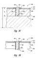
- FIG. 2is a schematic, side cross-sectional view of a microelectronic device 200 configured in accordance with an embodiment of the disclosure.
- the device 200includes a first microelectronic die 220 attached to a support member 202 , and a second microelectronic die 240 attached to the first die 220 in a stacked configuration.
- the device 200also includes an attachment feature or structure 260 between the first die 220 and the second die 240 .
- the attachment feature 260is configured to provide both a mechanical and an electrical connection between the first die 220 and the second die 240 , as described in greater detail below.
- the support member 202can include an interposer substrate, a printed circuit board, a lead frame, or another suitable support member.
- the support member 202can be composed of an organic material, a ceramic material, or another suitable dielectric material.
- the support member 202can include a first side 204 and a second side 206 opposite the first side 204 .
- the support member 202is an interposing device that provides an array of ball-pads for coupling very small contacts on the first and/or second dies 220 and 240 to another type of device (not shown).
- the support member 202for example, includes an array of support member terminals 208 at the first side 204 , an array of contact pads 210 (e.g., ball-pads) at the second side 206 , and a trace 212 or other type of conductive line between each support member terminal 208 and one or more corresponding contact pads 210 .
- the contact pads 210are arranged in an array for surface mounting the device 200 to a board or module of another device (not shown).
- a plurality of electrical couplers 216e.g., solder balls or conductive bumps
- the support member 202can include different features and/or the features can have a different arrangement.
- the first microelectronic die 220can be a semiconductor die or other type of microelectronic die.
- the first die 220can be a processor, a memory device (e.g., a DRAM or flash memory device), a sensor, a filter, or other type of microelectronic device.
- the first die 220includes an active or front side 222 and a back side 224 opposite the active side 222 .
- the active or front side 222generally refers to the side of the first die 220 that is accessed during formation of the active elements of the first die 220 .
- the first die 220also includes integrated circuitry 226 (shown schematically) and a plurality of terminals 228 (e.g., bond-pads) arranged in an array at the active side 222 and electrically coupled to the integrated circuitry 226 .
- the terminals 228accordingly provide external contacts to provide source voltages, ground voltages, and signals to the integrated circuitry 226 of the first die 220 .
- the terminals 228are typically so small that it is difficult to attach the terminals 228 directly to contacts on other devices in a cost-effective manner.
- the first die 220accordingly includes a redistribution structure or redistribution layer (RDL) 230 at the active side 222 to redistribute the signals from the terminals 228 to a larger array of contacts.
- RDLredistribution structure
- the redistribution structure 230can include one or more dielectric layers 232 , a plurality of peripheral contacts 234 at or proximate to a perimeter portion of the front or active side 222 , and a plurality of traces or other conductive lines (not shown) coupling at least a portion of the terminals 228 to corresponding peripheral contacts 234 .
- the peripheral contacts 234can be used to electrically couple the first die 220 to the support member terminals 208 of the support member 202 (e.g., using a chip-on-board (COB) configuration) with a plurality of wire bonds 236 or other types of connectors extending between the peripheral contacts 234 and corresponding support member terminals 208 .
- COBchip-on-board
- the redistribution structure 230can include different features and/or the features can have a different arrangement.
- the first die 220may not include the redistribution structure 230 .
- the device 200can further include an adhesive material 238 , such as an adhesive film, epoxy, tape, paste, or other suitable material disposed between the first die 220 and the support member 202 to help attach the first die 220 to the support member 202 .
- the second microelectronic die 240 stacked on the first die 220can be a semiconductor die or other type of microelectronic die.
- the second die 240can be a processor, a memory device (e.g., a DRAM or flash memory device), an imager, a sensor, a filter, or other type of microelectronic device.
- the second die 240includes an active or front side 242 and a back side 244 opposite the active side 242 .
- the second die 240also includes integrated circuitry 246 (shown schematically) and electrical connectors 248 (only one is shown) electrically coupled to the integrated circuitry 246 .
- the electrical connectors 248provide a small array of back side contacts within the footprint of the second die 240 .
- the individual connectors 248can include a terminal or bond site 250 (e.g., a bond-pad) and an interconnect 252 coupled to the terminal 250 .
- the terminal 250is at the front side 242 of the second die 240 and the interconnect 252 is a through-substrate or through-wafer interconnect that extends completely through the second die 240 to electrically couple the terminal 250 to corresponding features at the back side 244 .
- the terminal 250can be an internal feature that is embedded at an intermediate depth within the second die 240 and coupled to a corresponding interconnect 252 that extends through only a portion of the second die 240 .
- the first die 220 and/or the second die 240can have different features to perform different functions.
- the device 200can also include an encapsulant, shell, or cap 290 formed or otherwise deposited over the first and second dies 220 and 240 and at least a portion of the support member 202 .
- the encapsulant 290enhances the integrity of the device 200 and protects the first and second dies 220 and 240 and the physical and electrical connections between the dies 220 and 240 and the support member 202 from moisture, chemicals, and other contaminants.
- the device 200further includes the attachment feature 260 between the first die 220 and the second die 240 to physically and electrically attach the first and second dies together.
- the attachment feature 260can comprise a film-over-wire (FOW) die attach film applied over approximately the entire back side 244 of the second die 240 .
- the attachment feature 260is configured to protect the wire bonds 236 , the redistribution structure 230 , and other delicate front side components of the first die 220 from being damaged when the second die 240 is attached to the first die 220 using a die attachment process.
- the attachment feature 260further includes an interconnect structure or conductive coupler 272 extending at least partially through the attachment feature 260 and coupled to the interconnect 252 of the second die 240 .
- the interconnect structure 272is configured to electrically couple the interconnect 252 of the second die 240 to the terminals 228 of the first die 220 .
- the attachment feature 260 and its respective componentsare described in greater detail below with reference to FIGS. 3E-3G .
- microelectronic device 200 including the attachment feature 260may provide improved package reliability and robustness as compared with conventional stacked devices.
- Conventional devicestypically include an underfill material in a gap between an upper die and a lower die of the stacked device.
- the underfill materialis generally dispensed into the gap by injecting the underfill material along one or two sides of the device, and the material is drawn into the gap by capillary effects.
- One potential drawback with this approachis that it may result in a vulnerable mechanical connection between the two dies. For example, when the underfill material flows into the gap between the components, air bubbles, air pockets, and/or voids may form within the underfill material. During subsequent high temperature processes, the air trapped in these regions may expand and force the dies away from each other, damaging the mechanical and/or electrical connections between these components. This in turn often leads to failure or malfunction of such devices.
- attachment feature 260 of the device 200significantly reduce or eliminate the chances for air bubbles, air pockets, and/or voids to form in the gap between the two dies.
- the quality controlcan ensure the film or tape is at least substantially void free within the material of the film. Eliminating the underfill material between the first and second dies 220 and 240 is expected to provide a more robust and reliable connection between the components, thereby reducing and/or eliminating the tendency for the mechanical and/or electrical connections in the device 200 to fail.
- FIGS. 3A-4C described belowillustrate various embodiments of methods for forming attachment features on microelectronic dies. Although the following description illustrates only a single interconnect adjacent to a portion of the attachment feature, it will be appreciated that (a) a plurality of interconnects are constructed simultaneously through a plurality of dies on a wafer, and (b) the attachment feature is fabricated across all or a substantial portion of a workpiece.
- FIGS. 3A-3Gillustrate various stages of a method for forming one embodiment of the attachment feature 260 of FIG. 2 .
- FIG. 3Ais a schematic, side cross-sectional view of a portion of a microelectronic workpiece 300 at an early stage of this process after constructing a substantial portion of an embodiment of the interconnect 252 ( FIG. 2 ), but before constructing the attachment feature 260 .
- the workpiece 300includes a semiconductor substrate 302 having a front or active side 304 , a back side 306 , and a plurality of microelectronic dies (e.g., a plurality of second dies 240 of FIG. 2 ) formed on and/or in the substrate 302 .
- the workpiece 300can include several features generally similar to the workpiece 100 described above with reference to FIG. 1A .
- the substrate 302for example, can be a semiconductor wafer with the dies arranged in a die pattern on the wafer. In other embodiments, however, the workpiece 300 can have a different arrangement and/or include different features.
- the workpiece 300has first and second dielectric layers 310 and 312 over at least a portion of the front side 304 of the substrate 302 to protect the substrate 302 and the terminals 250 .
- the dielectric layers 310 and 312 and/or one or more of the subsequent dielectric layerscan be parylene, low temperature chemical vapor deposition (CVD) materials, such as silicon nitride (Si 3 Ni 4 ), silicon oxide (SiO 2 ), and/or other suitable dielectric materials.
- CVDlow temperature chemical vapor deposition
- the foregoing list of dielectric materialsis not exhaustive.
- the dielectric layers 310 and 312are not generally composed of the same material as each other, but these layers may be composed of the same material.
- one or both of the dielectric layers 310 and 312may be omitted and/or additional layers may be included.
- the workpiece 300also includes a plurality of vias or apertures 320 (only one is shown) formed through at least part of the substrate 302 using etching, laser drilling, or other suitable techniques.
- the illustrated vias 320are blind vias that extend only partially through the substrate 302 or are otherwise closed at one end. In other embodiments, however, the vias 320 can extend entirely through the workpiece 300 and/or the substrate 302 . Further details of representative methods for forming vias 320 are disclosed in U.S. Pat. No. 7,271,482, issued Sep. 18, 2007, and incorporated herein by reference in its entirety.
- the via 320is generally lined with another dielectric layer and one or more conductive layers (shown collectively as liner 314 ).
- the embodiment of the liner 314is shown schematically as a single layer, but in many embodiments the liner 314 has a number of different dielectric and conductive materials.
- the dielectric layer(s) of the liner 314electrically insulate the components in the substrate 302 from the interconnect that is subsequently formed in the via 320 .
- the dielectric layer(s) of the liner 314can include materials similar to those of the dielectric layers 310 and 312 described above.
- the conductive layer(s) of the liner 314can include tantalum (Ta), tungsten (W), copper (Cu), nickel (Ni), and/or other suitable conductive materials.
- a vent hole 325may be formed in the substrate 302 to extend from a bottom portion of each via 320 to the back side 306 of the substrate 302 .
- a conductive fill material 322is deposited into the via 320 to form the interconnect 252 .
- the fill material 322can include Cu, Ni, silver (Ag), gold (Au), solder, a conductive polymer, or other suitable materials or alloys of materials having the desired fill properties.
- the vent hole 325allows trapped air, gases, or volatile solvents to escape from the larger vias 320 when filling the vias with the conductive fill material 322 .
- the vent hole 325is an optional structure that may be omitted in several embodiments.
- the substrate 302is thinned from a first or initial thickness T 1 (shown in broken lines) to a second or final thickness T 2 by removing material from the back side 306 of the substrate 302 .
- a back side portion 326 of each interconnect 252is at least partially exposed after removing material from the back side 306 .
- the first thickness T 1 of the substrate 302is approximately 600 to 800 microns
- the second thickness T 2is approximately 50 to 100 microns.
- the initial and/or final thicknessescan be different in other embodiments.
- the back side 306 of the substrate 302can be thinned using chemical-mechanical planarization (CMP) processes, dry etching processes, chemical etching processes, chemical polishing, grinding procedures, or other suitable processes.
- CMPchemical-mechanical planarization
- the back side 306 of the substrate 302is etched back (e.g., using a dry etch or another suitable etching process) to further expose the back side portion 326 of the interconnect 252 , thus forming a conductive “post” or projection 330 .
- the etching processcan be used to offset the back side 306 of the substrate 302 from the end of the interconnect 252 to form the post 330 .
- the post 330has a height of approximately 10-30 microns above the back side 306 of the substrate 302 . In other embodiments, however, the post 330 may have a different height relative to the back side 306 .
- a film or layer 332is deposited onto the back side 306 to form a portion of the attachment feature 260 ( FIG. 2 ).
- the film materialcan be formed separately from the workpiece 300 and then applied onto desired portions of the workpiece 300 to form the film or layer 332 .
- a wafer-sized portion of film materiali.e., a portion of film material having a size and shape generally corresponding to that of the substrate 302 ) can be disposed over approximately the entire back side 306 .
- the film 332can be a FOW die attach film composed of a dielectric adhesive material (e.g., an epoxy resin) or another suitable material having the desired properties. Further details regarding suitable FOW die attach films are provided in U.S. Pat. No. 6,388,313, which is incorporated herein by reference in its entirety.
- the film 332can have a different size and/or configuration. In one embodiment, for example, the film 332 may be disposed over only a portion of the back side 306 of the substrate 302 .
- the film 332includes a plurality of preformed openings or apertures 334 (only one is shown) sized and positioned to expose at least a portion of the corresponding posts 330 .
- the opening 334has a diameter or cross-sectional dimension D greater than a diameter or cross-sectional dimension of the corresponding post 330 .
- the diameter D of the opening 334can be sized such that both the back side portion 326 of the corresponding interconnect 252 and at least a portion of the back side 306 of the substrate 302 adjacent to the interconnect 252 are exposed. In other embodiments, however, the openings 334 may have a different size and/or arrangement.
- the openings 334are preformed openings formed in the film 332 before the film material is applied onto the back side 306 of the substrate 302 .
- the openings 334can be formed in the film 332 using a punching or stamping process, an etching process, or another suitable process. In other embodiments, the openings 334 can be preformed in the film 332 using other suitable techniques. In still other embodiments, the openings 334 may be formed in the film 332 after the film 332 is applied onto the back side 306 (e.g., using an etching process). After applying the film 332 to the back side 306 , the film material can be cured (e.g., using a heat process) after application.
- one or more conductive layersare deposited into the opening 334 and in electrical contact with the post 330 to form the interconnect structures or conductive couplers 272 (only one is shown).
- the embodiment of the conductive layer 340is shown schematically as a single layer, but in many embodiments the layer 340 has a number of different conductive materials. Furthermore, although the layer 340 is shown at least approximately completely filling the opening 334 , in other embodiments the layer 340 may only fill a portion of the opening 334 .
- the conductive layer 340can include Cu, Ni, Au, palladium, Ag, solder, a conductive polymer, or other suitable materials or alloys of materials having the desired conductive properties.
- the layer 340can include a tri-layer arrangement of conductive materials.
- the three layersinclude a first layer of Cu plated onto the post 330 , a second layer of Ni plated onto the first layer, and a third layer of Au plated onto the second layer.
- the three layerscan include Ni, Au, and palladium.
- the layer 340may include a single layer of Cu in electrical contact with the post 330 .
- the layer 340can include other suitable material(s).
- FIG. 3Gis a bottom plan view of the portion of the workpiece 300 shown in FIG. 3F .
- an outer surface 341 of the interconnect structures 272is approximately co-planar or flush with a bottom surface 262 of the attachment feature 260 .
- the interconnect structures 272accordingly provide an external electrical connection to other electronic devices at the bottom surface 262 of the attachment feature 260 .
- the generally planar surface across the entire lower portion of the workpiece 300is expected to enable the attachment feature 260 to form reliable and robust mechanical and electrical connections with a corresponding device (e.g., the first die 220 of FIG. 2 ) in a stacked configuration without requiring an underfill material or additional electrical connectors.
- a corresponding devicee.g., the first die 220 of FIG. 2
- the interconnect structures 272are arranged in a generally linear arrangement and configured to transmit signals to and/or from one or more external devices (not shown). It will be appreciated, however, that the interconnect structures 272 can have a variety of different patterns or arrangements (e.g., a ball-grid array) depending upon the particular arrangement of electrical contacts at the back side 306 of the substrate 302 .
- the outer surface 341 of the conductive layer 340may not be co-planar with the bottom surface 262 of the attachment feature 260 .
- the outer surface 341may be recessed relative to the bottom surface 262 .
- one or more suitable electrical connectorse.g., a gold bump, solder ball, etc.—not shown in FIGS. 3F and 3G ) may be used to electrically and physically couple the interconnect structure 272 to the respective contacts on the corresponding microelectronic device (not shown).
- the outer surface 341may project outwardly a desired distance beyond the bottom surface 262 of the attachment feature 260 .
- the workpiece 300can be singulated to form a plurality of individual microelectronic dies (e.g., the second die 240 of FIG. 2 ).
- the attachment feature 260 at the back side 306 of the individual diescan be used to attach the dies to corresponding dies (e.g., the first die 220 of FIG. 2 ) in a stacked configuration.
- FIGS. 4A-4Care schematic, side cross-sectional views illustrating various stages of a method for forming the second die 240 and the attachment feature 260 of FIG. 2 in accordance with another embodiment of the disclosure.
- This methodbegins with the substrate 302 , the first dielectric layer 310 , the second dielectric layer 312 , and the terminal 250 .
- the initial stages of this methodare at least generally similar to the steps described above with reference to FIGS. 3A , and as such FIG. 4A shows a workpiece configuration similar to that illustrated in FIG. 3A .
- the process shown in FIGS. 4A-4Cdiffers from the method described above with respect to FIGS.
- the substrate 302can be thinned by removing material from the back side 306 of the substrate 302 until the substrate 302 has the desired thickness T 2 (e.g., approximately 50-100 microns).
- the substrate 302can be thinned using processes similar to those described above with reference to FIG. 3C (e.g., CMP processes, dry etching processes, etc.).
- FIG. 4Bis a schematic, side cross-sectional view of the substrate 302 after a blind hole or via 420 has been formed through the substrate 302 and the first dielectric layer 310 and in alignment with a corresponding terminal 250 .
- the hole 420is formed by patterning the back side 306 of the substrate 302 and etching through the substrate 302 from the back side 306 .
- the hole 420can be etched using one or more etching processes that selectively remove material from the substrate 302 and the first dielectric layer 310 compared to the terminal 250 .
- the hole 420can alternatively be formed using a laser in addition to or in lieu of etching. If a laser is used to form all or a portion of the hole 420 , it is typically cleaned using chemical cleaning agents to remove slag or other contaminants.
- the hole 420is generally lined with another dielectric layer and one or more conductive layers (shown collectively as liner 422 ). As with the liner 314 of FIG. 3A , the liner 422 is shown schematically as a single layer, but in many embodiments the liner 422 has a number of different dielectric and conductive materials. The liner 422 can include materials generally similar to the liner 314 described above. Referring next to FIG. 4C , a conductive fill material 424 is deposited into the hole 420 to form the interconnect 252 . The fill material 424 can be generally similar to the fill material 322 described above with reference to FIG. 3B .
- the fill material 424can be deposited into the hole 420 using a solder wave process, electroplating, electroless plating, or other suitable methods. After the fill material 424 has been deposited to form the interconnect 252 , the substrate 302 can undergo additional processing steps that are at least generally similar to those described above with reference to FIGS. 3D-3G to construct an attachment feature at the back side 306 of the substrate 302 .
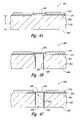
- FIG. 5is a schematic, side cross-sectional view of a packaged microelectronic device 500 configured in accordance with an embodiment of the disclosure.
- the device 500can include several features generally similar to the device 200 of FIG. 2 .
- the device 500includes plurality of microelectronic dies 540 (individually identified as a first microelectronic die 540 a and a second microelectronic die 540 b ) interconnected in a stacked-die arrangement with the attachment feature 260 .
- the first die 540 ais attached and electrically coupled to a support member 502 .
- the device 500differs from the device 200 described above in that the lower or bottom die in the stacked arrangement (i.e., the first die 540 a ) has a different configuration than the lower or bottom die (i.e., the first die 220 ) of the device 200 shown in FIG. 2 .
- the first and second dies 540 a and 540 bare at least approximately identical to each other.
- the first and second dies 540 a and 540 bcan have many components generally similar to the second microelectronic die 240 discussed above and illustrated in FIG. 2 .
- the first and second dies 540 a and 540 bcan include integrated circuitry 546 and connectors 548 electrically coupled to the integrated circuitry 546 .
- Each connector 548can include a terminal or bond site 550 (e.g., a bond pad) and an interconnect 552 coupled to the terminal 550 .
- the interconnects 552are through-substrate or through-wafer interconnects that extend completely through the respective dies to couple the terminal 550 to corresponding features at back sides 544 a and 544 b of the first and second dies 540 a and 540 b, respectively.
- the attachment feature 260provides both a physical and an electrical connection between the first and second dies 540 a and 540 b.
- the interconnect structure 272 of the attachment feature 260is coupled to a back side portion of the interconnect 552 of the second or upper die 540 b, and electrically couples the second die 540 b to the terminal 550 at a front or active side 542 a of the first die 540 a.
- the support member 502can be generally similar to the support member 202 described above with reference to FIG. 2 .
- the support member 502includes a first side 504 and a second side 506 opposite the first side 504 .
- the support member 502also includes an array of support member terminals 508 at the first side 504 , an array of contact pads 510 at the second side 506 , and a trace 512 or other type of conductive line between each support member terminal 508 and one or more corresponding contact pads 510 .
- the contact pads 510are arranged in an array for surface mounting the device 500 to a board or module of another device (not shown).
- a plurality of electrical couplers 516can be attached to corresponding contact pads 510 .
- the device 500can also include an encapsulant, shell, or cap 590 formed or otherwise deposited over the first and second dies 540 a and 540 b and at least a portion of the support member 502 .
- the microelectronic devices 200 and 500 or any one of the microelectronic devices formed using the methods described above with reference to FIGS. 1A-5can be. incorporated into any of a myriad of larger and/or more complex systems 600 , a representative one of which is shown schematically in FIG. 6 .
- the system 600can include a processor 602 , a memory 604 (e.g., SRAM, DRAM, DDR-SDRAM, flash memory, such as NAND flash memory or other types of flash memory, and/or other suitable memory devices), input/output devices 606 , and/or other subsystems or components 608 .
- Microelectronic devices and/or microfeature workpiecesmay be included in any of the components shown in FIG. 6 .
- the resulting system 600can perform any of a wide variety of computing, processing, storage, sensor, imagers, and/or other functions.
- representative systems 600include, without limitation, computers and/or other data processors, for example, desktop computers, laptop computers, Internet appliances, hand-held devices (e.g., palm-top computers, wearable computers, cellular or mobile phones, personal digital assistants), multi-processor systems, processor-based or programmable consumer electronics, network computers, and mini-computers.
- Other representative systems 600include cameras, light or other radiation sensors, servers and associated server subsystems, display devices, and/or memory devices.
- individual diescan include imager arrays, such as a CMOS imager.
- Components of the system 600may be housed in a single unit or distributed over multiple, interconnected units, e.g., through a communications network. Components can accordingly include local and/or remote memory storage devices and any of a wide variety of computer-readable media.
- attachment features described above with reference to particular embodimentscan include one or more additional features or components, or one or more of the features described above can be omitted.
- connections between the attachment feature, the interconnects, and other devicescan have arrangements different than those described above.
Landscapes
- Engineering & Computer Science (AREA)
- Microelectronics & Electronic Packaging (AREA)
- Power Engineering (AREA)
- Computer Hardware Design (AREA)
- Physics & Mathematics (AREA)
- Condensed Matter Physics & Semiconductors (AREA)
- General Physics & Mathematics (AREA)
- Manufacturing & Machinery (AREA)
- Internal Circuitry In Semiconductor Integrated Circuit Devices (AREA)
- Wire Bonding (AREA)
Abstract
Description
- The present disclosure is related to packaged microelectronic devices and methods for manufacturing packaged microelectronic devices.
- Packaged microelectronic assemblies, such as memory chips and microprocessor chips, typically include a microelectronic die mounted to a substrate and encased in a plastic protective covering. The die includes functional features, such as memory cells, processor circuits, and interconnecting circuitry. The die also typically includes bond pads electrically coupled to the functional features. The bond pads are electrically connected to pins or other types of terminals that extend outside the protective covering for connecting the die to busses, circuits, or other microelectronic assemblies. In one conventional arrangement, the die is mounted (e.g., face up or face down) to a supporting substrate (e.g., a printed circuit board), and the die bond pads are electrically coupled to corresponding bond pads of the substrate with wire bonds or metal bumps (e.g., solder balls or other suitable connections). After encapsulation, additional metal bumps can electrically connect the substrate to one or more external devices. Accordingly, the substrate supports the die and provides an electrical link between the die and the external devices.
- Die manufacturers have come under increasing pressure to reduce the volume occupied by the dies and yet increase the capacity of the resulting encapsulated assemblies. To meet these demands, die manufacturers often stack multiple dies on top of each other to increase the capacity or performance of the device within the limited surface area on the circuit board or other element to which the dies are mounted.
FIG. 1A is a partially schematic illustration of a representative microelectronic workpiece carrying microelectronic dies configured in accordance with embodiments of the disclosure.FIG. 1B is a schematic illustration of a microelectronic die singulated from the workpiece shown inFIG. 1A .FIG. 2 is a schematic, side cross-sectional view of a packaged microelectronic device configured in accordance with an embodiment of the disclosure.FIGS. 3A-3G illustrate various stages of a method for manufacturing a plurality of microelectronic devices having attachment features in accordance with an embodiment of the disclosure.FIGS. 4A-4C illustrate various stages of a method for manufacturing a plurality of microelectronic devices in accordance with another embodiment of the disclosure.FIG. 5 is a schematic, side cross-sectional view of a packaged microelectronic device configured in accordance with still another embodiment of the disclosure.FIG. 6 is a schematic illustration of a system that can include one or more microelectronic devices configured in accordance with embodiments of the disclosure.- Specific details of several embodiments of the disclosure are described below with reference to packaged microelectronic devices and methods for manufacturing such devices. The microelectronic devices described below include two microelectronic dies attached to each other in a stacked configuration, but in other embodiments the microelectronic devices can have three or more stacked microelectronic dies electrically coupled to each other and, in some cases, a support member. The microelectronic devices can include, for example, micromechanical components, data storage elements, optics, read/write components, or other features. The microelectronic dies can be SRAM, DRAM (e.g., DDR-SDRAM), flash memory (e.g., NAND flash memory), processors, imagers, and other types of devices. The term “interconnect” may encompass various types of conductive structures that extend at least partially through a substrate of a microelectronic die or another component and electrically couple together conductive contacts located at opposing ends of the interconnect. Substrates can be semiconductive pieces (e.g., doped silicon wafers, gallium arsenide wafers, or other semiconductor wafers), nonconductive pieces (e.g., various ceramic substrates), or conductive pieces. Moreover, several other embodiments of the disclosure can have configurations, components, or procedures different than those described in this section. A person of ordinary skill in the art, therefore, will accordingly understand that the disclosure may have other embodiments with additional elements, or the disclosure may have other embodiments without several of the elements shown and described below with reference to
FIGS. 2-6 . FIG. 1A is amicroelectronic workpiece 100 in the form of asemiconductor wafer 110 that includes multiplemicroelectronic dies 120. At least some of the processes described below may be conducted on themicroelectronic workpiece 100 at the wafer level, and other processes may be conducted on the individualmicroelectronic dies 120 of themicroelectronic workpiece 100 after thedies 120 have been singulated from thelarger wafer 110. Accordingly, unless otherwise noted, structures and methods described below in the context of a microelectronic workpiece can apply to thewafer 110, thedies 120 that are formed from thewafer 110, and/or an assembly of one ormore dies 120 in a stacked-die configuration or attached to a support member.FIG. 1B is a schematic illustration of anindividual die 120 after it has been singulated from thewafer 110 shown inFIG. 1A . The die120 can include operable microelectronic structures, optionally encased within a protective encapsulant. The die120 can be electrically connected to external structural devices by pins, bond pads, solder balls, redistribution structures, and/or other conductive structures.FIG. 2 is a schematic, side cross-sectional view of amicroelectronic device 200 configured in accordance with an embodiment of the disclosure. Thedevice 200 includes a firstmicroelectronic die 220 attached to asupport member 202, and a secondmicroelectronic die 240 attached to thefirst die 220 in a stacked configuration. Thedevice 200 also includes an attachment feature orstructure 260 between thefirst die 220 and thesecond die 240. Theattachment feature 260 is configured to provide both a mechanical and an electrical connection between thefirst die 220 and thesecond die 240, as described in greater detail below.- The
support member 202 can include an interposer substrate, a printed circuit board, a lead frame, or another suitable support member. Thesupport member 202 can be composed of an organic material, a ceramic material, or another suitable dielectric material. Thesupport member 202 can include afirst side 204 and asecond side 206 opposite thefirst side 204. In the illustrated embodiment, thesupport member 202 is an interposing device that provides an array of ball-pads for coupling very small contacts on the first and/orsecond dies support member 202, for example, includes an array ofsupport member terminals 208 at thefirst side 204, an array of contact pads210 (e.g., ball-pads) at thesecond side 206, and atrace 212 or other type of conductive line between eachsupport member terminal 208 and one or morecorresponding contact pads 210. Thecontact pads 210 are arranged in an array for surface mounting thedevice 200 to a board or module of another device (not shown). A plurality of electrical couplers216 (e.g., solder balls or conductive bumps) can be attached tocorresponding contact pads 210. In other embodiments, thesupport member 202 can include different features and/or the features can have a different arrangement. - The first microelectronic die220 can be a semiconductor die or other type of microelectronic die. The
first die 220, for example, can be a processor, a memory device (e.g., a DRAM or flash memory device), a sensor, a filter, or other type of microelectronic device. Thefirst die 220 includes an active orfront side 222 and aback side 224 opposite theactive side 222. The active orfront side 222 generally refers to the side of thefirst die 220 that is accessed during formation of the active elements of thefirst die 220. Thefirst die 220 also includes integrated circuitry226 (shown schematically) and a plurality of terminals228 (e.g., bond-pads) arranged in an array at theactive side 222 and electrically coupled to the integratedcircuitry 226. Theterminals 228 accordingly provide external contacts to provide source voltages, ground voltages, and signals to the integratedcircuitry 226 of thefirst die 220. Theterminals 228, however, are typically so small that it is difficult to attach theterminals 228 directly to contacts on other devices in a cost-effective manner. The first die220 accordingly includes a redistribution structure or redistribution layer (RDL)230 at theactive side 222 to redistribute the signals from theterminals 228 to a larger array of contacts. - The
redistribution structure 230, for example, can include one or moredielectric layers 232, a plurality ofperipheral contacts 234 at or proximate to a perimeter portion of the front oractive side 222, and a plurality of traces or other conductive lines (not shown) coupling at least a portion of theterminals 228 to correspondingperipheral contacts 234. Theperipheral contacts 234 can be used to electrically couple thefirst die 220 to thesupport member terminals 208 of the support member202 (e.g., using a chip-on-board (COB) configuration) with a plurality ofwire bonds 236 or other types of connectors extending between theperipheral contacts 234 and correspondingsupport member terminals 208. In other embodiments, theredistribution structure 230 can include different features and/or the features can have a different arrangement. In still other embodiments, thefirst die 220 may not include theredistribution structure 230. In several embodiments, thedevice 200 can further include anadhesive material 238, such as an adhesive film, epoxy, tape, paste, or other suitable material disposed between thefirst die 220 and thesupport member 202 to help attach thefirst die 220 to thesupport member 202. - The second microelectronic die240 stacked on the
first die 220 can be a semiconductor die or other type of microelectronic die. Thesecond die 240, for example, can be a processor, a memory device (e.g., a DRAM or flash memory device), an imager, a sensor, a filter, or other type of microelectronic device. Thesecond die 240 includes an active orfront side 242 and a back side244 opposite theactive side 242. Thesecond die 240 also includes integrated circuitry246 (shown schematically) and electrical connectors248 (only one is shown) electrically coupled to theintegrated circuitry 246. - The
electrical connectors 248 provide a small array of back side contacts within the footprint of thesecond die 240. Theindividual connectors 248, for example, can include a terminal or bond site250 (e.g., a bond-pad) and aninterconnect 252 coupled to the terminal250. In the embodiment illustrated inFIG. 2 , the terminal250 is at thefront side 242 of thesecond die 240 and theinterconnect 252 is a through-substrate or through-wafer interconnect that extends completely through thesecond die 240 to electrically couple the terminal250 to corresponding features at the back side244. In other embodiments, however, the terminal250 can be an internal feature that is embedded at an intermediate depth within thesecond die 240 and coupled to acorresponding interconnect 252 that extends through only a portion of thesecond die 240. In other embodiments, thefirst die 220 and/or thesecond die 240 can have different features to perform different functions. - The
device 200 can also include an encapsulant, shell, or cap290 formed or otherwise deposited over the first and second dies220 and240 and at least a portion of thesupport member 202. Theencapsulant 290 enhances the integrity of thedevice 200 and protects the first and second dies220 and240 and the physical and electrical connections between the dies220 and240 and thesupport member 202 from moisture, chemicals, and other contaminants. - As mentioned previously, the
device 200 further includes theattachment feature 260 between thefirst die 220 and thesecond die 240 to physically and electrically attach the first and second dies together. In several embodiments, theattachment feature 260 can comprise a film-over-wire (FOW) die attach film applied over approximately the entire back side244 of thesecond die 240. Theattachment feature 260 is configured to protect thewire bonds 236, theredistribution structure 230, and other delicate front side components of thefirst die 220 from being damaged when thesecond die 240 is attached to thefirst die 220 using a die attachment process. Theattachment feature 260 further includes an interconnect structure orconductive coupler 272 extending at least partially through theattachment feature 260 and coupled to theinterconnect 252 of thesecond die 240. Theinterconnect structure 272 is configured to electrically couple theinterconnect 252 of thesecond die 240 to theterminals 228 of thefirst die 220. Theattachment feature 260 and its respective components are described in greater detail below with reference toFIGS. 3E-3G . - Several embodiments of the
microelectronic device 200 including theattachment feature 260 may provide improved package reliability and robustness as compared with conventional stacked devices. Conventional devices, for example, typically include an underfill material in a gap between an upper die and a lower die of the stacked device. The underfill material is generally dispensed into the gap by injecting the underfill material along one or two sides of the device, and the material is drawn into the gap by capillary effects. One potential drawback with this approach, however, is that it may result in a vulnerable mechanical connection between the two dies. For example, when the underfill material flows into the gap between the components, air bubbles, air pockets, and/or voids may form within the underfill material. During subsequent high temperature processes, the air trapped in these regions may expand and force the dies away from each other, damaging the mechanical and/or electrical connections between these components. This in turn often leads to failure or malfunction of such devices. - Unlike conventional stacked devices (which typically include underfill material between the upper and lower dies), several embodiments of the
attachment feature 260 of thedevice 200 significantly reduce or eliminate the chances for air bubbles, air pockets, and/or voids to form in the gap between the two dies. For example, when theattachment feature 260 is a preformed film or tape, the quality control can ensure the film or tape is at least substantially void free within the material of the film. Eliminating the underfill material between the first and second dies220 and240 is expected to provide a more robust and reliable connection between the components, thereby reducing and/or eliminating the tendency for the mechanical and/or electrical connections in thedevice 200 to fail. - In the embodiment illustrated in
FIG. 2 , formation of thedevice 200 including theattachment feature 260 between the first and second dies220 and240 is complete.FIGS. 3A-4C described below illustrate various embodiments of methods for forming attachment features on microelectronic dies. Although the following description illustrates only a single interconnect adjacent to a portion of the attachment feature, it will be appreciated that (a) a plurality of interconnects are constructed simultaneously through a plurality of dies on a wafer, and (b) the attachment feature is fabricated across all or a substantial portion of a workpiece. FIGS. 3A-3G illustrate various stages of a method for forming one embodiment of theattachment feature 260 ofFIG. 2 .FIG. 3A , more specifically, is a schematic, side cross-sectional view of a portion of amicroelectronic workpiece 300 at an early stage of this process after constructing a substantial portion of an embodiment of the interconnect252 (FIG. 2 ), but before constructing theattachment feature 260. Theworkpiece 300 includes asemiconductor substrate 302 having a front oractive side 304, aback side 306, and a plurality of microelectronic dies (e.g., a plurality of second dies240 ofFIG. 2 ) formed on and/or in thesubstrate 302. Theworkpiece 300 can include several features generally similar to theworkpiece 100 described above with reference toFIG. 1A . Thesubstrate 302, for example, can be a semiconductor wafer with the dies arranged in a die pattern on the wafer. In other embodiments, however, theworkpiece 300 can have a different arrangement and/or include different features.- The
workpiece 300 has first and seconddielectric layers front side 304 of thesubstrate 302 to protect thesubstrate 302 and theterminals 250. Thedielectric layers dielectric layers dielectric layers - The
workpiece 300 also includes a plurality of vias or apertures320 (only one is shown) formed through at least part of thesubstrate 302 using etching, laser drilling, or other suitable techniques. The illustratedvias 320 are blind vias that extend only partially through thesubstrate 302 or are otherwise closed at one end. In other embodiments, however, thevias 320 can extend entirely through theworkpiece 300 and/or thesubstrate 302. Further details of representative methods for formingvias 320 are disclosed in U.S. Pat. No. 7,271,482, issued Sep. 18, 2007, and incorporated herein by reference in its entirety. - The via320 is generally lined with another dielectric layer and one or more conductive layers (shown collectively as liner314). The embodiment of the
liner 314 is shown schematically as a single layer, but in many embodiments theliner 314 has a number of different dielectric and conductive materials. The dielectric layer(s) of theliner 314 electrically insulate the components in thesubstrate 302 from the interconnect that is subsequently formed in thevia 320. The dielectric layer(s) of theliner 314 can include materials similar to those of thedielectric layers liner 314 can include tantalum (Ta), tungsten (W), copper (Cu), nickel (Ni), and/or other suitable conductive materials. After lining the via320, avent hole 325 may be formed in thesubstrate 302 to extend from a bottom portion of each via320 to theback side 306 of thesubstrate 302. - Referring next to
FIG. 3B , aconductive fill material 322 is deposited into the via320 to form theinterconnect 252. Thefill material 322 can include Cu, Ni, silver (Ag), gold (Au), solder, a conductive polymer, or other suitable materials or alloys of materials having the desired fill properties. Thevent hole 325 allows trapped air, gases, or volatile solvents to escape from thelarger vias 320 when filling the vias with theconductive fill material 322. Thevent hole 325 is an optional structure that may be omitted in several embodiments. - Referring next to
FIG. 3C , thesubstrate 302 is thinned from a first or initial thickness T1(shown in broken lines) to a second or final thickness T2by removing material from theback side 306 of thesubstrate 302. In the illustrated embodiment, aback side portion 326 of eachinterconnect 252 is at least partially exposed after removing material from theback side 306. In one embodiment, the first thickness T1of thesubstrate 302 is approximately 600 to 800 microns, and the second thickness T2is approximately 50 to 100 microns. The initial and/or final thicknesses can be different in other embodiments. Theback side 306 of thesubstrate 302 can be thinned using chemical-mechanical planarization (CMP) processes, dry etching processes, chemical etching processes, chemical polishing, grinding procedures, or other suitable processes. - Referring to
FIG. 3D , theback side 306 of thesubstrate 302 is etched back (e.g., using a dry etch or another suitable etching process) to further expose theback side portion 326 of theinterconnect 252, thus forming a conductive “post” orprojection 330. In other embodiments, other suitable processes in addition to, or in lieu of, the etching process can be used to offset theback side 306 of thesubstrate 302 from the end of theinterconnect 252 to form thepost 330. In one embodiment, thepost 330 has a height of approximately 10-30 microns above theback side 306 of thesubstrate 302. In other embodiments, however, thepost 330 may have a different height relative to theback side 306. - Referring next to
FIG. 3E , after forming thepost 330, a film orlayer 332 is deposited onto theback side 306 to form a portion of the attachment feature260 (FIG. 2 ). In one embodiment, the film material can be formed separately from theworkpiece 300 and then applied onto desired portions of theworkpiece 300 to form the film orlayer 332. For example, a wafer-sized portion of film material (i.e., a portion of film material having a size and shape generally corresponding to that of the substrate302) can be disposed over approximately the entireback side 306. As mentioned previously, for example, thefilm 332 can be a FOW die attach film composed of a dielectric adhesive material (e.g., an epoxy resin) or another suitable material having the desired properties. Further details regarding suitable FOW die attach films are provided in U.S. Pat. No. 6,388,313, which is incorporated herein by reference in its entirety. Alternatively, thefilm 332 can have a different size and/or configuration. In one embodiment, for example, thefilm 332 may be disposed over only a portion of theback side 306 of thesubstrate 302. - The
film 332 includes a plurality of preformed openings or apertures334 (only one is shown) sized and positioned to expose at least a portion of the corresponding posts330. In the illustrated embodiment, for example, theopening 334 has a diameter or cross-sectional dimension D greater than a diameter or cross-sectional dimension of thecorresponding post 330. The diameter D of theopening 334 can be sized such that both theback side portion 326 of thecorresponding interconnect 252 and at least a portion of theback side 306 of thesubstrate 302 adjacent to theinterconnect 252 are exposed. In other embodiments, however, theopenings 334 may have a different size and/or arrangement. - As mentioned above, the
openings 334 are preformed openings formed in thefilm 332 before the film material is applied onto theback side 306 of thesubstrate 302. Theopenings 334, for example, can be formed in thefilm 332 using a punching or stamping process, an etching process, or another suitable process. In other embodiments, theopenings 334 can be preformed in thefilm 332 using other suitable techniques. In still other embodiments, theopenings 334 may be formed in thefilm 332 after thefilm 332 is applied onto the back side306 (e.g., using an etching process). After applying thefilm 332 to theback side 306, the film material can be cured (e.g., using a heat process) after application. - Referring next to
FIG. 3F , one or more conductive layers (shown collectively as layer340) are deposited into theopening 334 and in electrical contact with thepost 330 to form the interconnect structures or conductive couplers272 (only one is shown). The embodiment of theconductive layer 340 is shown schematically as a single layer, but in many embodiments thelayer 340 has a number of different conductive materials. Furthermore, although thelayer 340 is shown at least approximately completely filling theopening 334, in other embodiments thelayer 340 may only fill a portion of theopening 334. Theconductive layer 340 can include Cu, Ni, Au, palladium, Ag, solder, a conductive polymer, or other suitable materials or alloys of materials having the desired conductive properties. In one particular embodiment, for example, thelayer 340 can include a tri-layer arrangement of conductive materials. The three layers include a first layer of Cu plated onto thepost 330, a second layer of Ni plated onto the first layer, and a third layer of Au plated onto the second layer. In another particular embodiment having a tri-layer arrangement, the three layers can include Ni, Au, and palladium. In still another embodiment, thelayer 340 may include a single layer of Cu in electrical contact with thepost 330. In yet other embodiments, thelayer 340 can include other suitable material(s). FIG. 3G is a bottom plan view of the portion of theworkpiece 300 shown inFIG. 3F . Referring toFIGS. 3F and 3G together, anouter surface 341 of theinterconnect structures 272 is approximately co-planar or flush with abottom surface 262 of theattachment feature 260. Theinterconnect structures 272 accordingly provide an external electrical connection to other electronic devices at thebottom surface 262 of theattachment feature 260. The generally planar surface across the entire lower portion of theworkpiece 300 is expected to enable theattachment feature 260 to form reliable and robust mechanical and electrical connections with a corresponding device (e.g., thefirst die 220 ofFIG. 2 ) in a stacked configuration without requiring an underfill material or additional electrical connectors. In the embodiment shown inFIG. 3G , theinterconnect structures 272 are arranged in a generally linear arrangement and configured to transmit signals to and/or from one or more external devices (not shown). It will be appreciated, however, that theinterconnect structures 272 can have a variety of different patterns or arrangements (e.g., a ball-grid array) depending upon the particular arrangement of electrical contacts at theback side 306 of thesubstrate 302.- In other embodiments, the
outer surface 341 of theconductive layer 340 may not be co-planar with thebottom surface 262 of theattachment feature 260. In one embodiment, for example, theouter surface 341 may be recessed relative to thebottom surface 262. In this arrangement, one or more suitable electrical connectors (e.g., a gold bump, solder ball, etc.—not shown inFIGS. 3F and 3G ) may be used to electrically and physically couple theinterconnect structure 272 to the respective contacts on the corresponding microelectronic device (not shown). In still another embodiment, theouter surface 341 may project outwardly a desired distance beyond thebottom surface 262 of theattachment feature 260. - After forming the
attachment feature 260 at theback side 306 of thesubstrate 302, theworkpiece 300 can be singulated to form a plurality of individual microelectronic dies (e.g., thesecond die 240 ofFIG. 2 ). The attachment feature260 at theback side 306 of the individual dies can be used to attach the dies to corresponding dies (e.g., thefirst die 220 ofFIG. 2 ) in a stacked configuration. FIGS. 4A-4C are schematic, side cross-sectional views illustrating various stages of a method for forming thesecond die 240 and theattachment feature 260 ofFIG. 2 in accordance with another embodiment of the disclosure. This method begins with thesubstrate 302, thefirst dielectric layer 310, thesecond dielectric layer 312, and the terminal250. The initial stages of this method are at least generally similar to the steps described above with reference toFIGS. 3A , and as suchFIG. 4A shows a workpiece configuration similar to that illustrated inFIG. 3A . The process shown inFIGS. 4A-4C , however, differs from the method described above with respect toFIGS. 3A-3G in that a hole or via is formed from theback side 306 of thesubstrate 302 instead of thefront side 304. Before forming the blind hole, thesubstrate 302 can be thinned by removing material from theback side 306 of thesubstrate 302 until thesubstrate 302 has the desired thickness T2(e.g., approximately 50-100 microns). Thesubstrate 302 can be thinned using processes similar to those described above with reference toFIG. 3C (e.g., CMP processes, dry etching processes, etc.).FIG. 4B is a schematic, side cross-sectional view of thesubstrate 302 after a blind hole or via420 has been formed through thesubstrate 302 and thefirst dielectric layer 310 and in alignment with acorresponding terminal 250. Thehole 420 is formed by patterning theback side 306 of thesubstrate 302 and etching through thesubstrate 302 from theback side 306. Thehole 420 can be etched using one or more etching processes that selectively remove material from thesubstrate 302 and thefirst dielectric layer 310 compared to the terminal250. Thehole 420 can alternatively be formed using a laser in addition to or in lieu of etching. If a laser is used to form all or a portion of thehole 420, it is typically cleaned using chemical cleaning agents to remove slag or other contaminants.- After forming the
hole 420, thehole 420 is generally lined with another dielectric layer and one or more conductive layers (shown collectively as liner422). As with theliner 314 ofFIG. 3A , theliner 422 is shown schematically as a single layer, but in many embodiments theliner 422 has a number of different dielectric and conductive materials. Theliner 422 can include materials generally similar to theliner 314 described above. Referring next toFIG. 4C , aconductive fill material 424 is deposited into thehole 420 to form theinterconnect 252. Thefill material 424 can be generally similar to thefill material 322 described above with reference toFIG. 3B . Thefill material 424 can be deposited into thehole 420 using a solder wave process, electroplating, electroless plating, or other suitable methods. After thefill material 424 has been deposited to form theinterconnect 252, thesubstrate 302 can undergo additional processing steps that are at least generally similar to those described above with reference toFIGS. 3D-3G to construct an attachment feature at theback side 306 of thesubstrate 302. FIG. 5 is a schematic, side cross-sectional view of a packagedmicroelectronic device 500 configured in accordance with an embodiment of the disclosure. Thedevice 500 can include several features generally similar to thedevice 200 ofFIG. 2 . For example, thedevice 500 includes plurality of microelectronic dies540 (individually identified as a first microelectronic die540aand a second microelectronic die540b) interconnected in a stacked-die arrangement with theattachment feature 260. The first die540ais attached and electrically coupled to asupport member 502. Thedevice 500 differs from thedevice 200 described above in that the lower or bottom die in the stacked arrangement (i.e., thefirst die 540a) has a different configuration than the lower or bottom die (i.e., the first die220) of thedevice 200 shown inFIG. 2 . In this embodiment, for example, the first and second dies540aand540bare at least approximately identical to each other.- The first and second dies540aand540bcan have many components generally similar to the second microelectronic die240 discussed above and illustrated in
FIG. 2 . For example, the first and second dies540aand540bcan includeintegrated circuitry 546 andconnectors 548 electrically coupled to theintegrated circuitry 546. Eachconnector 548 can include a terminal or bond site550 (e.g., a bond pad) and aninterconnect 552 coupled to the terminal550. Theinterconnects 552 are through-substrate or through-wafer interconnects that extend completely through the respective dies to couple the terminal550 to corresponding features at back sides544aand544bof the first and second dies540aand540b,respectively. Theattachment feature 260 provides both a physical and an electrical connection between the first and second dies540aand540b.For example, theinterconnect structure 272 of theattachment feature 260 is coupled to a back side portion of theinterconnect 552 of the second orupper die 540b,and electrically couples thesecond die 540bto the terminal550 at a front oractive side 542aof thefirst die 540a. - The
support member 502 can be generally similar to thesupport member 202 described above with reference toFIG. 2 . For example, thesupport member 502 includes afirst side 504 and asecond side 506 opposite thefirst side 504. Thesupport member 502 also includes an array ofsupport member terminals 508 at thefirst side 504, an array ofcontact pads 510 at thesecond side 506, and atrace 512 or other type of conductive line between eachsupport member terminal 508 and one or morecorresponding contact pads 510. Thecontact pads 510 are arranged in an array for surface mounting thedevice 500 to a board or module of another device (not shown). A plurality of electrical couplers516 (e.g., solder balls or conductive bumps) can be attached tocorresponding contact pads 510. Thedevice 500 can also include an encapsulant, shell, or cap590 formed or otherwise deposited over the first and second dies540aand540band at least a portion of thesupport member 502. - The
microelectronic devices FIGS. 1A-5 can be. incorporated into any of a myriad of larger and/or morecomplex systems 600, a representative one of which is shown schematically inFIG. 6 . Thesystem 600 can include aprocessor 602, a memory604 (e.g., SRAM, DRAM, DDR-SDRAM, flash memory, such as NAND flash memory or other types of flash memory, and/or other suitable memory devices), input/output devices 606, and/or other subsystems orcomponents 608. Microelectronic devices and/or microfeature workpieces (e.g., in the form of microfeature dies and/or combinations of microfeature dies) may be included in any of the components shown inFIG. 6 . The resultingsystem 600 can perform any of a wide variety of computing, processing, storage, sensor, imagers, and/or other functions. Accordingly,representative systems 600 include, without limitation, computers and/or other data processors, for example, desktop computers, laptop computers, Internet appliances, hand-held devices (e.g., palm-top computers, wearable computers, cellular or mobile phones, personal digital assistants), multi-processor systems, processor-based or programmable consumer electronics, network computers, and mini-computers. Otherrepresentative systems 600 include cameras, light or other radiation sensors, servers and associated server subsystems, display devices, and/or memory devices. In such systems, individual dies can include imager arrays, such as a CMOS imager. Components of thesystem 600 may be housed in a single unit or distributed over multiple, interconnected units, e.g., through a communications network. Components can accordingly include local and/or remote memory storage devices and any of a wide variety of computer-readable media. - From the foregoing, it will be appreciated that specific embodiments of the disclosure have been described herein for purposes of illustration, but that various modifications may be made without deviating from the spirit and scope of the disclosure. For example, structures and/or processes described in the context of particular embodiments may be combined or eliminated in other embodiments. In particular, the attachment features described above with reference to particular embodiments can include one or more additional features or components, or one or more of the features described above can be omitted. Further, the connections between the attachment feature, the interconnects, and other devices (e.g., bond pads, conductive couplers, and/or external devices) can have arrangements different than those described above. Moreover, while advantages associated with certain embodiments of the disclosure have been described in the context of these embodiments, other embodiments may also exhibit such advantages, and not all embodiments need necessarily exhibit such advantages to fall within the scope of the disclosure. Accordingly, embodiments of the disclosure are not limited except as by the appended claims.
Claims (21)
Priority Applications (5)
| Application Number | Priority Date | Filing Date | Title |
|---|---|---|---|
| US12/136,717US7745920B2 (en) | 2008-06-10 | 2008-06-10 | Packaged microelectronic devices and methods for manufacturing packaged microelectronic devices |
| US12/796,740US8148807B2 (en) | 2008-06-10 | 2010-06-09 | Packaged microelectronic devices and associated systems |
| US13/298,140US8940581B2 (en) | 2008-06-10 | 2011-11-16 | Packaged microelectronic devices and methods for manufacturing packaged microelectronic devices |
| US14/604,545US9530748B2 (en) | 2008-06-10 | 2015-01-23 | Packaged microelectronic devices and methods for manufacturing packaged microelectronic devices |
| US15/388,166US10008468B2 (en) | 2008-06-10 | 2016-12-22 | Packaged microelectronic devices and methods for manufacturing packaged microelectronic devices |
Applications Claiming Priority (1)
| Application Number | Priority Date | Filing Date | Title |
|---|---|---|---|
| US12/136,717US7745920B2 (en) | 2008-06-10 | 2008-06-10 | Packaged microelectronic devices and methods for manufacturing packaged microelectronic devices |
Related Child Applications (1)
| Application Number | Title | Priority Date | Filing Date |
|---|---|---|---|
| US12/796,740DivisionUS8148807B2 (en) | 2008-06-10 | 2010-06-09 | Packaged microelectronic devices and associated systems |
Publications (2)
| Publication Number | Publication Date |
|---|---|
| US20090302484A1true US20090302484A1 (en) | 2009-12-10 |
| US7745920B2 US7745920B2 (en) | 2010-06-29 |
Family
ID=41399576
Family Applications (5)
| Application Number | Title | Priority Date | Filing Date |
|---|---|---|---|
| US12/136,717ActiveUS7745920B2 (en) | 2008-06-10 | 2008-06-10 | Packaged microelectronic devices and methods for manufacturing packaged microelectronic devices |
| US12/796,740ActiveUS8148807B2 (en) | 2008-06-10 | 2010-06-09 | Packaged microelectronic devices and associated systems |
| US13/298,140Active2028-07-30US8940581B2 (en) | 2008-06-10 | 2011-11-16 | Packaged microelectronic devices and methods for manufacturing packaged microelectronic devices |
| US14/604,545Active2028-07-31US9530748B2 (en) | 2008-06-10 | 2015-01-23 | Packaged microelectronic devices and methods for manufacturing packaged microelectronic devices |
| US15/388,166ActiveUS10008468B2 (en) | 2008-06-10 | 2016-12-22 | Packaged microelectronic devices and methods for manufacturing packaged microelectronic devices |
Family Applications After (4)
| Application Number | Title | Priority Date | Filing Date |
|---|---|---|---|
| US12/796,740ActiveUS8148807B2 (en) | 2008-06-10 | 2010-06-09 | Packaged microelectronic devices and associated systems |
| US13/298,140Active2028-07-30US8940581B2 (en) | 2008-06-10 | 2011-11-16 | Packaged microelectronic devices and methods for manufacturing packaged microelectronic devices |
| US14/604,545Active2028-07-31US9530748B2 (en) | 2008-06-10 | 2015-01-23 | Packaged microelectronic devices and methods for manufacturing packaged microelectronic devices |
| US15/388,166ActiveUS10008468B2 (en) | 2008-06-10 | 2016-12-22 | Packaged microelectronic devices and methods for manufacturing packaged microelectronic devices |
Country Status (1)
| Country | Link |
|---|---|
| US (5) | US7745920B2 (en) |
Cited By (55)
| Publication number | Priority date | Publication date | Assignee | Title |
|---|---|---|---|---|
| US20080179734A1 (en)* | 2007-01-25 | 2008-07-31 | Samsung Electronics Co., Ltd. | Stacked package, method of manufacturing the same, and memory card having the stacked package |
| US20100244272A1 (en)* | 2008-06-10 | 2010-09-30 | Micron Technology, Inc. | Packaged microelectronic devices and methods for manufacturing packaged microelectronic devices |
| US20120292786A1 (en)* | 2010-01-21 | 2012-11-22 | International Business Machines Corporation | Integrated void fill for through silicon via |
| EP2750185A1 (en)* | 2012-12-27 | 2014-07-02 | Commissariat à l'Énergie Atomique et aux Énergies Alternatives | Improved method for manufacturing a contact structure |
| US8922021B2 (en)* | 2011-12-30 | 2014-12-30 | Deca Technologies Inc. | Die up fully molded fan-out wafer level packaging |
| US8930647B1 (en) | 2011-04-06 | 2015-01-06 | P4tents1, LLC | Multiple class memory systems |
| US9158546B1 (en) | 2011-04-06 | 2015-10-13 | P4tents1, LLC | Computer program product for fetching from a first physical memory between an execution of a plurality of threads associated with a second physical memory |
| US9164679B2 (en) | 2011-04-06 | 2015-10-20 | Patents1, Llc | System, method and computer program product for multi-thread operation involving first memory of a first memory class and second memory of a second memory class |
| US9170744B1 (en) | 2011-04-06 | 2015-10-27 | P4tents1, LLC | Computer program product for controlling a flash/DRAM/embedded DRAM-equipped system |
| US9177926B2 (en) | 2011-12-30 | 2015-11-03 | Deca Technologies Inc | Semiconductor device and method comprising thickened redistribution layers |
| US9176671B1 (en) | 2011-04-06 | 2015-11-03 | P4tents1, LLC | Fetching data between thread execution in a flash/DRAM/embedded DRAM-equipped system |
| US9337086B2 (en) | 2011-12-30 | 2016-05-10 | Deca Technologies Inc. | Die up fully molded fan-out wafer level packaging |
| US9417754B2 (en) | 2011-08-05 | 2016-08-16 | P4tents1, LLC | User interface system, method, and computer program product |
| US9432298B1 (en) | 2011-12-09 | 2016-08-30 | P4tents1, LLC | System, method, and computer program product for improving memory systems |
| US9576919B2 (en) | 2011-12-30 | 2017-02-21 | Deca Technologies Inc. | Semiconductor device and method comprising redistribution layers |
| US9613830B2 (en) | 2011-12-30 | 2017-04-04 | Deca Technologies Inc. | Fully molded peripheral package on package device |
| US9831170B2 (en) | 2011-12-30 | 2017-11-28 | Deca Technologies, Inc. | Fully molded miniaturized semiconductor module |
| US10050004B2 (en) | 2015-11-20 | 2018-08-14 | Deca Technologies Inc. | Fully molded peripheral package on package device |
| US10312195B2 (en)* | 2017-07-14 | 2019-06-04 | Samsung Electro-Mechanics Co., Ltd. | Fan-out semiconductor package |
| US10373870B2 (en) | 2010-02-16 | 2019-08-06 | Deca Technologies Inc. | Semiconductor device and method of packaging |
| US10672624B2 (en) | 2011-12-30 | 2020-06-02 | Deca Technologies Inc. | Method of making fully molded peripheral package on package device |
| US20200176347A1 (en)* | 2018-11-29 | 2020-06-04 | Qorvo Us, Inc. | Thermally enhanced package and process for making the same |
| US20200235054A1 (en) | 2019-01-23 | 2020-07-23 | Qorvo Us, Inc. | Rf devices with enhanced performance and methods of forming the same |
| US10749518B2 (en) | 2016-11-18 | 2020-08-18 | Qorvo Us, Inc. | Stacked field-effect transistor switch |
| US10755992B2 (en) | 2017-07-06 | 2020-08-25 | Qorvo Us, Inc. | Wafer-level packaging for enhanced performance |
| US10773952B2 (en) | 2016-05-20 | 2020-09-15 | Qorvo Us, Inc. | Wafer-level package with enhanced performance |
| US10784233B2 (en) | 2017-09-05 | 2020-09-22 | Qorvo Us, Inc. | Microelectronics package with self-aligned stacked-die assembly |
| US10784149B2 (en) | 2016-05-20 | 2020-09-22 | Qorvo Us, Inc. | Air-cavity module with enhanced device isolation |
| US10790216B2 (en) | 2016-12-09 | 2020-09-29 | Qorvo Us, Inc. | Thermally enhanced semiconductor package and process for making the same |
| US10804246B2 (en) | 2018-06-11 | 2020-10-13 | Qorvo Us, Inc. | Microelectronics package with vertically stacked dies |
| US10804179B2 (en) | 2016-08-12 | 2020-10-13 | Qorvo Us, Inc. | Wafer-level package with enhanced performance |
| US10964554B2 (en) | 2018-10-10 | 2021-03-30 | Qorvo Us, Inc. | Wafer-level fan-out package with enhanced performance |
| US10978426B2 (en)* | 2018-12-31 | 2021-04-13 | Micron Technology, Inc. | Semiconductor packages with pass-through clock traces and associated systems and methods |
| US10985033B2 (en) | 2016-09-12 | 2021-04-20 | Qorvo Us, Inc. | Semiconductor package with reduced parasitic coupling effects and process for making the same |
| US11056453B2 (en) | 2019-06-18 | 2021-07-06 | Deca Technologies Usa, Inc. | Stackable fully molded semiconductor structure with vertical interconnects |
| US11069590B2 (en) | 2018-10-10 | 2021-07-20 | Qorvo Us, Inc. | Wafer-level fan-out package with enhanced performance |
| US11152363B2 (en) | 2018-03-28 | 2021-10-19 | Qorvo Us, Inc. | Bulk CMOS devices with enhanced performance and methods of forming the same utilizing bulk CMOS process |
| CN113574662A (en)* | 2019-03-19 | 2021-10-29 | 美光科技公司 | Interposer, microelectronic device assembly including interposer, and method of manufacture |
| US11189535B2 (en)* | 2015-07-09 | 2021-11-30 | Samsung Electronics Co., Ltd. | Semiconductor chip including chip pad, redistribution wiring test pad, and redistribution wiring connection pad |
| CN113745120A (en)* | 2020-05-29 | 2021-12-03 | 弗劳恩霍夫应用研究促进协会 | Microelectronic device and method of manufacturing the same |
| US20220108938A1 (en) | 2019-01-23 | 2022-04-07 | Qorvo Us, Inc. | Rf devices with enhanced performance and methods of forming the same |
| US11302706B2 (en)* | 2019-04-30 | 2022-04-12 | Yangtze Memory Technologies Co., Ltd. | Bonded unified semiconductor chips and fabrication and operation methods thereof |
| US20220139862A1 (en) | 2019-01-23 | 2022-05-05 | Qorvo Us, Inc. | Rf devices with enhanced performance and methods of forming the same |
| US11387157B2 (en) | 2019-01-23 | 2022-07-12 | Qorvo Us, Inc. | RF devices with enhanced performance and methods of forming the same |
| US11646289B2 (en) | 2019-12-02 | 2023-05-09 | Qorvo Us, Inc. | RF devices with enhanced performance and methods of forming the same |
| US11923238B2 (en) | 2019-12-12 | 2024-03-05 | Qorvo Us, Inc. | Method of forming RF devices with enhanced performance including attaching a wafer to a support carrier by a bonding technique without any polymer adhesive |
| US12046505B2 (en) | 2018-04-20 | 2024-07-23 | Qorvo Us, Inc. | RF devices with enhanced performance and methods of forming the same utilizing localized SOI formation |
| US12046535B2 (en) | 2018-07-02 | 2024-07-23 | Qorvo Us, Inc. | RF devices with enhanced performance and methods of forming the same |
| US12046483B2 (en) | 2019-01-23 | 2024-07-23 | Qorvo Us, Inc. | RF devices with enhanced performance and methods of forming the same |
| US12062701B2 (en) | 2018-04-04 | 2024-08-13 | Qorvo Us, Inc. | Gallium-nitride-based module with enhanced electrical performance and process for making the same |
| US12062571B2 (en) | 2021-03-05 | 2024-08-13 | Qorvo Us, Inc. | Selective etching process for SiGe and doped epitaxial silicon |
| US12074086B2 (en) | 2019-11-01 | 2024-08-27 | Qorvo Us, Inc. | RF devices with nanotube particles for enhanced performance and methods of forming the same |
| US12125825B2 (en) | 2019-01-23 | 2024-10-22 | Qorvo Us, Inc. | RF devices with enhanced performance and methods of forming the same |
| US12129168B2 (en) | 2019-12-23 | 2024-10-29 | Qorvo Us, Inc. | Microelectronics package with vertically stacked MEMS device and controller device |
| US12438065B2 (en) | 2021-07-01 | 2025-10-07 | Deca Technologies Usa, Inc. | Fully molded semiconductor structure with through silicon via (TSV) vertical interconnects |
Families Citing this family (51)
| Publication number | Priority date | Publication date | Assignee | Title |
|---|---|---|---|---|
| US8286046B2 (en) | 2001-09-28 | 2012-10-09 | Rambus Inc. | Integrated circuit testing module including signal shaping interface |
| US8063650B2 (en) | 2002-11-27 | 2011-11-22 | Rambus Inc. | Testing fuse configurations in semiconductor devices |
| US7701045B2 (en) | 2006-04-11 | 2010-04-20 | Rambus Inc. | Point-to-point connection topology for stacked devices |
| US9899312B2 (en)* | 2006-04-13 | 2018-02-20 | Rambus Inc. | Isolating electric paths in semiconductor device packages |
| US7768847B2 (en) | 2008-04-09 | 2010-08-03 | Rambus Inc. | Programmable memory repair scheme |
| US8310051B2 (en) | 2008-05-27 | 2012-11-13 | Mediatek Inc. | Package-on-package with fan-out WLCSP |
| US20100213589A1 (en)* | 2009-02-20 | 2010-08-26 | Tung-Hsien Hsieh | Multi-chip package |
| CN102097490A (en)* | 2009-12-15 | 2011-06-15 | 中芯国际集成电路制造(上海)有限公司 | Method for manufacturing double-bit flash memory |
| US20110204517A1 (en)* | 2010-02-23 | 2011-08-25 | Qualcomm Incorporated | Semiconductor Device with Vias Having More Than One Material |
| FR2957481B1 (en)* | 2010-03-10 | 2012-08-31 | Commissariat Energie Atomique | INTERCONNECTION STRUCTURE COMPRISING VIAS BORGNES FOR METALLIZATION |
| US8421245B2 (en) | 2010-12-22 | 2013-04-16 | Intel Corporation | Substrate with embedded stacked through-silicon via die |
| US8853072B2 (en)* | 2011-06-06 | 2014-10-07 | Micron Technology, Inc. | Methods of forming through-substrate interconnects |
| US8502390B2 (en) | 2011-07-12 | 2013-08-06 | Tessera, Inc. | De-skewed multi-die packages |
| US8513817B2 (en) | 2011-07-12 | 2013-08-20 | Invensas Corporation | Memory module in a package |
| US8823165B2 (en) | 2011-07-12 | 2014-09-02 | Invensas Corporation | Memory module in a package |
| US9153508B2 (en) | 2011-08-17 | 2015-10-06 | Rambus Inc. | Multi-chip package and interposer with signal line compression |
| US9524957B2 (en) | 2011-08-17 | 2016-12-20 | Intersil Americas LLC | Back-to-back stacked dies |
| US9570196B2 (en) | 2011-09-01 | 2017-02-14 | Rambus Inc. | Testing through-silicon-vias |
| TWI515864B (en) | 2011-10-03 | 2016-01-01 | 英帆薩斯公司 | Stub minimization with terminal grids offset from center of package |
| US8525327B2 (en) | 2011-10-03 | 2013-09-03 | Invensas Corporation | Stub minimization for assemblies without wirebonds to package substrate |
| KR101894823B1 (en) | 2011-10-03 | 2018-09-04 | 인벤사스 코포레이션 | Stub minimization for multi-die wirebond assemblies with parallel windows |
| US8436477B2 (en) | 2011-10-03 | 2013-05-07 | Invensas Corporation | Stub minimization using duplicate sets of signal terminals in assemblies without wirebonds to package substrate |
| JP5947904B2 (en) | 2011-10-03 | 2016-07-06 | インヴェンサス・コーポレイション | Stub minimization for multi-die wirebond assemblies with orthogonal windows |
| US8653646B2 (en) | 2011-10-03 | 2014-02-18 | Invensas Corporation | Stub minimization using duplicate sets of terminals for wirebond assemblies without windows |
| US8405207B1 (en) | 2011-10-03 | 2013-03-26 | Invensas Corporation | Stub minimization for wirebond assemblies without windows |
| US8436457B2 (en) | 2011-10-03 | 2013-05-07 | Invensas Corporation | Stub minimization for multi-die wirebond assemblies with parallel windows |
| US8441111B2 (en) | 2011-10-03 | 2013-05-14 | Invensas Corporation | Stub minimization for multi-die wirebond assemblies with parallel windows |
| US8345441B1 (en) | 2011-10-03 | 2013-01-01 | Invensas Corporation | Stub minimization for multi-die wirebond assemblies with parallel windows |
| US8848392B2 (en) | 2012-08-27 | 2014-09-30 | Invensas Corporation | Co-support module and microelectronic assembly |
| US9368477B2 (en) | 2012-08-27 | 2016-06-14 | Invensas Corporation | Co-support circuit panel and microelectronic packages |
| US8787034B2 (en) | 2012-08-27 | 2014-07-22 | Invensas Corporation | Co-support system and microelectronic assembly |
| US8848391B2 (en) | 2012-08-27 | 2014-09-30 | Invensas Corporation | Co-support component and microelectronic assembly |
| US9070423B2 (en) | 2013-06-11 | 2015-06-30 | Invensas Corporation | Single package dual channel memory with co-support |
| KR101546575B1 (en) | 2013-08-12 | 2015-08-21 | 앰코 테크놀로지 코리아 주식회사 | Semiconductor Package And Fabricating Method Thereof |
| US9123555B2 (en) | 2013-10-25 | 2015-09-01 | Invensas Corporation | Co-support for XFD packaging |
| US9771256B2 (en)* | 2014-06-29 | 2017-09-26 | Taiwan Semiconductor Manufacturing Company Limited | Micro electro mechanical system (MEMS) device having via extending through plug |
| US9281296B2 (en) | 2014-07-31 | 2016-03-08 | Invensas Corporation | Die stacking techniques in BGA memory package for small footprint CPU and memory motherboard design |
| US9691437B2 (en) | 2014-09-25 | 2017-06-27 | Invensas Corporation | Compact microelectronic assembly having reduced spacing between controller and memory packages |
| TWI582926B (en)* | 2015-08-11 | 2017-05-11 | 旺宏電子股份有限公司 | Connector structure and method for fabricating the same |
| US9484080B1 (en) | 2015-11-09 | 2016-11-01 | Invensas Corporation | High-bandwidth memory application with controlled impedance loading |
| US9449871B1 (en) | 2015-11-18 | 2016-09-20 | International Business Machines Corporation | Hybrid airgap structure with oxide liner |
| US9679613B1 (en) | 2016-05-06 | 2017-06-13 | Invensas Corporation | TFD I/O partition for high-speed, high-density applications |
| US11069606B2 (en) | 2016-10-06 | 2021-07-20 | Compass Technology Company Limited | Fabrication process and structure of fine pitch traces for a solid state diffusion bond on flip chip interconnect |
| US10103095B2 (en) | 2016-10-06 | 2018-10-16 | Compass Technology Company Limited | Fabrication process and structure of fine pitch traces for a solid state diffusion bond on flip chip interconnect |
| US10923449B2 (en) | 2016-10-06 | 2021-02-16 | Compass Technology Company Limited | Fabrication process and structure of fine pitch traces for a solid state diffusion bond on flip chip interconnect |
| US9923059B1 (en) | 2017-02-20 | 2018-03-20 | Silanna Asia Pte Ltd | Connection arrangements for integrated lateral diffusion field effect transistors |
| US10083897B2 (en) | 2017-02-20 | 2018-09-25 | Silanna Asia Pte Ltd | Connection arrangements for integrated lateral diffusion field effect transistors having a backside contact |
| US10468342B2 (en) | 2018-02-02 | 2019-11-05 | Compass Technology Company, Ltd. | Formation of fine pitch traces using ultra-thin PAA modified fully additive process |
| US10636734B2 (en) | 2018-02-02 | 2020-04-28 | Compass Technology Company, Ltd. | Formation of fine pitch traces using ultra-thin PAA modified fully additive process |
| US20240079369A1 (en)* | 2022-09-06 | 2024-03-07 | Micron Technology, Inc. | Connecting semiconductor dies through traces |
| US12356724B2 (en)* | 2023-11-08 | 2025-07-08 | Myeong-Eun Hwang | Double-sided integrated circuit die and integrated circuit package including the same |
Citations (14)
| Publication number | Priority date | Publication date | Assignee | Title |
|---|---|---|---|---|
| US6388313B1 (en)* | 2001-01-30 | 2002-05-14 | Siliconware Precision Industries Co., Ltd. | Multi-chip module |
| US20030030151A1 (en)* | 2001-08-03 | 2003-02-13 | Seiko Epson Corporation | Semiconductor device and method for manufacturing the same |
| US6650007B2 (en)* | 1998-06-30 | 2003-11-18 | Micron Technology, Inc. | Stackable ceramic fbga for high thermal applications |
| US6734549B2 (en)* | 2001-07-03 | 2004-05-11 | Matsushita Electric Industrial Co., Ltd. | Semiconductor device having a device for testing the semiconductor |
| US6784023B2 (en)* | 1996-05-20 | 2004-08-31 | Micron Technology, Inc. | Method of fabrication of stacked semiconductor devices |
| US6867500B2 (en)* | 2002-04-08 | 2005-03-15 | Micron Technology, Inc. | Multi-chip module and methods |
| US6914259B2 (en)* | 2001-10-03 | 2005-07-05 | Matsushita Electric Industrial Co., Ltd. | Multi-chip module, semiconductor chip, and interchip connection test method for multi-chip module |
| US6919627B2 (en)* | 2002-06-04 | 2005-07-19 | Siliconware Precision Industries Co., Ltd. | Multichip module |
| US20060202319A1 (en)* | 2004-08-19 | 2006-09-14 | Swee Seng Eric T | Assemblies and multi-chip modules including stacked semiconductor dice having centrally located, wire bonded bond pads |
| US7335533B2 (en)* | 2001-10-15 | 2008-02-26 | Micron Technology, Inc. | Methods for assembling semiconductor devices in superimposed relation with adhesive material defining the distance adjacent semiconductor devices are spaced apart from one another |
| US20080203554A1 (en)* | 2003-12-25 | 2008-08-28 | Elpida Memory Inc. | Semiconductor integrated circuit device |
| US20080237824A1 (en)* | 2006-02-17 | 2008-10-02 | Amkor Technology, Inc. | Stacked electronic component package having single-sided film spacer |
| US20090085220A1 (en)* | 2007-09-28 | 2009-04-02 | Qimonda Ag | Semiconductor component and method of manufacturing |
| US7535102B2 (en)* | 1999-03-01 | 2009-05-19 | Megica Corporation | High performance sub-system design and assembly |
Family Cites Families (42)
| Publication number | Priority date | Publication date | Assignee | Title |
|---|---|---|---|---|
| JP2002009236A (en)* | 2000-06-21 | 2002-01-11 | Shinko Electric Ind Co Ltd | Multiple layer semiconductor device and its manufacturing method |
| JP3951091B2 (en)* | 2000-08-04 | 2007-08-01 | セイコーエプソン株式会社 | Manufacturing method of semiconductor device |
| US6528869B1 (en)* | 2001-04-06 | 2003-03-04 | Amkor Technology, Inc. | Semiconductor package with molded substrate and recessed input/output terminals |
| US6555917B1 (en)* | 2001-10-09 | 2003-04-29 | Amkor Technology, Inc. | Semiconductor package having stacked semiconductor chips and method of making the same |
| US6599778B2 (en)* | 2001-12-19 | 2003-07-29 | International Business Machines Corporation | Chip and wafer integration process using vertical connections |
| JP3910493B2 (en)* | 2002-06-14 | 2007-04-25 | 新光電気工業株式会社 | Semiconductor device and manufacturing method thereof |
| US6969914B2 (en)* | 2002-08-29 | 2005-11-29 | Micron Technology, Inc. | Electronic device package |
| US7354798B2 (en)* | 2002-12-20 | 2008-04-08 | International Business Machines Corporation | Three-dimensional device fabrication method |
| JP4072677B2 (en)* | 2003-01-15 | 2008-04-09 | セイコーエプソン株式会社 | Semiconductor chip, semiconductor wafer, semiconductor device and manufacturing method thereof, circuit board, and electronic equipment |
| JP2004228392A (en)* | 2003-01-24 | 2004-08-12 | Seiko Epson Corp | Method of manufacturing semiconductor device and method of manufacturing semiconductor module |
| SG137651A1 (en)* | 2003-03-14 | 2007-12-28 | Micron Technology Inc | Microelectronic devices and methods for packaging microelectronic devices |
| TW594950B (en)* | 2003-03-18 | 2004-06-21 | United Epitaxy Co Ltd | Light emitting diode and package scheme and method thereof |
| JP3646720B2 (en)* | 2003-06-19 | 2005-05-11 | セイコーエプソン株式会社 | Semiconductor device and manufacturing method thereof, circuit board, and electronic apparatus |
| JP3646719B2 (en)* | 2003-06-19 | 2005-05-11 | セイコーエプソン株式会社 | Semiconductor device and manufacturing method thereof, circuit board, and electronic apparatus |
| US6934065B2 (en)* | 2003-09-18 | 2005-08-23 | Micron Technology, Inc. | Microelectronic devices and methods for packaging microelectronic devices |
| KR100535181B1 (en)* | 2003-11-18 | 2005-12-09 | 삼성전자주식회사 | Semiconductor chip package having decoupling capacitor and manufacturing method thereof |
| US7049170B2 (en)* | 2003-12-17 | 2006-05-23 | Tru-Si Technologies, Inc. | Integrated circuits and packaging substrates with cavities, and attachment methods including insertion of protruding contact pads into cavities |
| JP4063796B2 (en)* | 2004-06-30 | 2008-03-19 | 日本電気株式会社 | Multilayer semiconductor device |
| ITTO20040899A1 (en)* | 2004-12-23 | 2005-03-23 | St Microelectronics Srl | PORTABLE APPARATUS EQUIPPED WITH AN ACCELEROMETRIC DEVICE FOR FREE FALL DETECTION |
| US7807505B2 (en)* | 2005-08-30 | 2010-10-05 | Micron Technology, Inc. | Methods for wafer-level packaging of microfeature devices and microfeature devices formed using such methods |
| JP4509972B2 (en)* | 2005-09-01 | 2010-07-21 | 日本特殊陶業株式会社 | Wiring board, embedded ceramic chip |
| US7633157B2 (en)* | 2005-12-13 | 2009-12-15 | Micron Technology, Inc. | Microelectronic devices having a curved surface and methods for manufacturing the same |
| SG133445A1 (en)* | 2005-12-29 | 2007-07-30 | Micron Technology Inc | Methods for packaging microelectronic devices and microelectronic devices formed using such methods |
| US8411450B2 (en)* | 2006-01-25 | 2013-04-02 | Nec Corporation | Electronic device package, module, and electronic device |
| KR100753415B1 (en)* | 2006-03-17 | 2007-08-30 | 주식회사 하이닉스반도체 | Stack package |
| US7952184B2 (en)* | 2006-08-31 | 2011-05-31 | Micron Technology, Inc. | Distributed semiconductor device methods, apparatus, and systems |
| SG143098A1 (en)* | 2006-12-04 | 2008-06-27 | Micron Technology Inc | Packaged microelectronic devices and methods for manufacturing packaged microelectronic devices |
| KR100844997B1 (en)* | 2006-12-29 | 2008-07-09 | 삼성전자주식회사 | Semiconductor package, semiconductor stack package, method of manufacturing the packages |
| KR100880242B1 (en)* | 2007-01-16 | 2009-01-28 | 삼성전자주식회사 | Semiconductor device stack package and method for forming the same |
| KR100827667B1 (en)* | 2007-01-16 | 2008-05-07 | 삼성전자주식회사 | A semiconductor package having a semiconductor chip in a substrate and a method of manufacturing the same |
| TWI357640B (en)* | 2007-01-24 | 2012-02-01 | Siliconware Precision Industries Co Ltd | Multichip stacking structure and fabricating metho |
| US7638869B2 (en)* | 2007-03-28 | 2009-12-29 | Qimonda Ag | Semiconductor device |
| US20080237881A1 (en)* | 2007-03-30 | 2008-10-02 | Tony Dambrauskas | Recessed solder socket in a semiconductor substrate |
| TWI330868B (en)* | 2007-04-13 | 2010-09-21 | Siliconware Precision Industries Co Ltd | Semiconductor device and manufacturing method thereof |
| US8367471B2 (en)* | 2007-06-15 | 2013-02-05 | Micron Technology, Inc. | Semiconductor assemblies, stacked semiconductor devices, and methods of manufacturing semiconductor assemblies and stacked semiconductor devices |
| US20080315331A1 (en)* | 2007-06-25 | 2008-12-25 | Robert Gideon Wodnicki | Ultrasound system with through via interconnect structure |
| KR100963617B1 (en)* | 2007-11-30 | 2010-06-16 | 주식회사 하이닉스반도체 | Semiconductor package and manufacturing method thereof |
| US8084854B2 (en)* | 2007-12-28 | 2011-12-27 | Micron Technology, Inc. | Pass-through 3D interconnect for microelectronic dies and associated systems and methods |
| US7821107B2 (en)* | 2008-04-22 | 2010-10-26 | Micron Technology, Inc. | Die stacking with an annular via having a recessed socket |
| US8178976B2 (en)* | 2008-05-12 | 2012-05-15 | Texas Instruments Incorporated | IC device having low resistance TSV comprising ground connection |
| US8253230B2 (en)* | 2008-05-15 | 2012-08-28 | Micron Technology, Inc. | Disabling electrical connections using pass-through 3D interconnects and associated systems and methods |
| US7745920B2 (en) | 2008-06-10 | 2010-06-29 | Micron Technology, Inc. | Packaged microelectronic devices and methods for manufacturing packaged microelectronic devices |
- 2008
- 2008-06-10USUS12/136,717patent/US7745920B2/enactiveActive
- 2010
- 2010-06-09USUS12/796,740patent/US8148807B2/enactiveActive
- 2011
- 2011-11-16USUS13/298,140patent/US8940581B2/enactiveActive
- 2015
- 2015-01-23USUS14/604,545patent/US9530748B2/enactiveActive
- 2016
- 2016-12-22USUS15/388,166patent/US10008468B2/enactiveActive
Patent Citations (15)
| Publication number | Priority date | Publication date | Assignee | Title |
|---|---|---|---|---|
| US6784023B2 (en)* | 1996-05-20 | 2004-08-31 | Micron Technology, Inc. | Method of fabrication of stacked semiconductor devices |
| US6650007B2 (en)* | 1998-06-30 | 2003-11-18 | Micron Technology, Inc. | Stackable ceramic fbga for high thermal applications |
| US7535102B2 (en)* | 1999-03-01 | 2009-05-19 | Megica Corporation | High performance sub-system design and assembly |
| US6388313B1 (en)* | 2001-01-30 | 2002-05-14 | Siliconware Precision Industries Co., Ltd. | Multi-chip module |
| US6734549B2 (en)* | 2001-07-03 | 2004-05-11 | Matsushita Electric Industrial Co., Ltd. | Semiconductor device having a device for testing the semiconductor |
| US20030030151A1 (en)* | 2001-08-03 | 2003-02-13 | Seiko Epson Corporation | Semiconductor device and method for manufacturing the same |
| US6914259B2 (en)* | 2001-10-03 | 2005-07-05 | Matsushita Electric Industrial Co., Ltd. | Multi-chip module, semiconductor chip, and interchip connection test method for multi-chip module |
| US7335533B2 (en)* | 2001-10-15 | 2008-02-26 | Micron Technology, Inc. | Methods for assembling semiconductor devices in superimposed relation with adhesive material defining the distance adjacent semiconductor devices are spaced apart from one another |
| US6867500B2 (en)* | 2002-04-08 | 2005-03-15 | Micron Technology, Inc. | Multi-chip module and methods |
| US6919627B2 (en)* | 2002-06-04 | 2005-07-19 | Siliconware Precision Industries Co., Ltd. | Multichip module |
| US20080203554A1 (en)* | 2003-12-25 | 2008-08-28 | Elpida Memory Inc. | Semiconductor integrated circuit device |
| US20060202319A1 (en)* | 2004-08-19 | 2006-09-14 | Swee Seng Eric T | Assemblies and multi-chip modules including stacked semiconductor dice having centrally located, wire bonded bond pads |
| US7492039B2 (en)* | 2004-08-19 | 2009-02-17 | Micron Technology, Inc. | Assemblies and multi-chip modules including stacked semiconductor dice having centrally located, wire bonded bond pads |
| US20080237824A1 (en)* | 2006-02-17 | 2008-10-02 | Amkor Technology, Inc. | Stacked electronic component package having single-sided film spacer |
| US20090085220A1 (en)* | 2007-09-28 | 2009-04-02 | Qimonda Ag | Semiconductor component and method of manufacturing |
Cited By (139)
| Publication number | Priority date | Publication date | Assignee | Title |
|---|---|---|---|---|
| US20080179734A1 (en)* | 2007-01-25 | 2008-07-31 | Samsung Electronics Co., Ltd. | Stacked package, method of manufacturing the same, and memory card having the stacked package |
| US8940581B2 (en) | 2008-06-10 | 2015-01-27 | Micron Technology, Inc. | Packaged microelectronic devices and methods for manufacturing packaged microelectronic devices |
| US20100244272A1 (en)* | 2008-06-10 | 2010-09-30 | Micron Technology, Inc. | Packaged microelectronic devices and methods for manufacturing packaged microelectronic devices |
| US8148807B2 (en) | 2008-06-10 | 2012-04-03 | Micron Technology, Inc. | Packaged microelectronic devices and associated systems |
| US10008468B2 (en) | 2008-06-10 | 2018-06-26 | Micron Technology, Inc. | Packaged microelectronic devices and methods for manufacturing packaged microelectronic devices |
| US9530748B2 (en) | 2008-06-10 | 2016-12-27 | Micron Technology, Inc. | Packaged microelectronic devices and methods for manufacturing packaged microelectronic devices |
| US20120292786A1 (en)* | 2010-01-21 | 2012-11-22 | International Business Machines Corporation | Integrated void fill for through silicon via |
| US8633580B2 (en)* | 2010-01-21 | 2014-01-21 | International Business Machines Corporation | Integrated void fill for through silicon via |
| US10373870B2 (en) | 2010-02-16 | 2019-08-06 | Deca Technologies Inc. | Semiconductor device and method of packaging |
| US8930647B1 (en) | 2011-04-06 | 2015-01-06 | P4tents1, LLC | Multiple class memory systems |
| US9158546B1 (en) | 2011-04-06 | 2015-10-13 | P4tents1, LLC | Computer program product for fetching from a first physical memory between an execution of a plurality of threads associated with a second physical memory |
| US9164679B2 (en) | 2011-04-06 | 2015-10-20 | Patents1, Llc | System, method and computer program product for multi-thread operation involving first memory of a first memory class and second memory of a second memory class |
| US9170744B1 (en) | 2011-04-06 | 2015-10-27 | P4tents1, LLC | Computer program product for controlling a flash/DRAM/embedded DRAM-equipped system |
| US9223507B1 (en) | 2011-04-06 | 2015-12-29 | P4tents1, LLC | System, method and computer program product for fetching data between an execution of a plurality of threads |
| US9176671B1 (en) | 2011-04-06 | 2015-11-03 | P4tents1, LLC | Fetching data between thread execution in a flash/DRAM/embedded DRAM-equipped system |
| US9182914B1 (en) | 2011-04-06 | 2015-11-10 | P4tents1, LLC | System, method and computer program product for multi-thread operation involving first memory of a first memory class and second memory of a second memory class |
| US9189442B1 (en) | 2011-04-06 | 2015-11-17 | P4tents1, LLC | Fetching data between thread execution in a flash/DRAM/embedded DRAM-equipped system |
| US9195395B1 (en) | 2011-04-06 | 2015-11-24 | P4tents1, LLC | Flash/DRAM/embedded DRAM-equipped system and method |
| US10656757B1 (en) | 2011-08-05 | 2020-05-19 | P4tents1, LLC | Gesture-equipped touch screen system, method, and computer program product |
| US10534474B1 (en) | 2011-08-05 | 2020-01-14 | P4tents1, LLC | Gesture-equipped touch screen system, method, and computer program product |
| US9417754B2 (en) | 2011-08-05 | 2016-08-16 | P4tents1, LLC | User interface system, method, and computer program product |
| US10838542B1 (en) | 2011-08-05 | 2020-11-17 | P4tents1, LLC | Gesture-equipped touch screen system, method, and computer program product |
| US10936114B1 (en) | 2011-08-05 | 2021-03-02 | P4tents1, LLC | Gesture-equipped touch screen system, method, and computer program product |
| US10788931B1 (en) | 2011-08-05 | 2020-09-29 | P4tents1, LLC | Devices, methods, and graphical user interfaces for manipulating user interface objects with visual and/or haptic feedback |
| US10782819B1 (en) | 2011-08-05 | 2020-09-22 | P4tents1, LLC | Gesture-equipped touch screen system, method, and computer program product |
| US10996787B1 (en) | 2011-08-05 | 2021-05-04 | P4tents1, LLC | Gesture-equipped touch screen system, method, and computer program product |
| US11061503B1 (en) | 2011-08-05 | 2021-07-13 | P4tents1, LLC | Devices, methods, and graphical user interfaces for manipulating user interface objects with visual and/or haptic feedback |
| US10031607B1 (en) | 2011-08-05 | 2018-07-24 | P4tents1, LLC | System, method, and computer program product for a multi-pressure selection touch screen |
| US10725581B1 (en) | 2011-08-05 | 2020-07-28 | P4tents1, LLC | Devices, methods and graphical user interfaces for manipulating user interface objects with visual and/or haptic feedback |
| US10120480B1 (en) | 2011-08-05 | 2018-11-06 | P4tents1, LLC | Application-specific pressure-sensitive touch screen system, method, and computer program product |
| US10146353B1 (en) | 2011-08-05 | 2018-12-04 | P4tents1, LLC | Touch screen system, method, and computer program product |
| US10156921B1 (en) | 2011-08-05 | 2018-12-18 | P4tents1, LLC | Tri-state gesture-equipped touch screen system, method, and computer program product |
| US10162448B1 (en) | 2011-08-05 | 2018-12-25 | P4tents1, LLC | System, method, and computer program product for a pressure-sensitive touch screen for messages |
| US10203794B1 (en) | 2011-08-05 | 2019-02-12 | P4tents1, LLC | Pressure-sensitive home interface system, method, and computer program product |
| US10209806B1 (en) | 2011-08-05 | 2019-02-19 | P4tents1, LLC | Tri-state gesture-equipped touch screen system, method, and computer program product |
| US10209807B1 (en) | 2011-08-05 | 2019-02-19 | P4tents1, LLC | Pressure sensitive touch screen system, method, and computer program product for hyperlinks |
| US10209808B1 (en) | 2011-08-05 | 2019-02-19 | P4tents1, LLC | Pressure-based interface system, method, and computer program product with virtual display layers |
| US10209809B1 (en) | 2011-08-05 | 2019-02-19 | P4tents1, LLC | Pressure-sensitive touch screen system, method, and computer program product for objects |
| US10222891B1 (en) | 2011-08-05 | 2019-03-05 | P4tents1, LLC | Setting interface system, method, and computer program product for a multi-pressure selection touch screen |
| US10222892B1 (en) | 2011-08-05 | 2019-03-05 | P4tents1, LLC | System, method, and computer program product for a multi-pressure selection touch screen |
| US10222894B1 (en) | 2011-08-05 | 2019-03-05 | P4tents1, LLC | System, method, and computer program product for a multi-pressure selection touch screen |
| US10222893B1 (en) | 2011-08-05 | 2019-03-05 | P4tents1, LLC | Pressure-based touch screen system, method, and computer program product with virtual display layers |
| US10222895B1 (en) | 2011-08-05 | 2019-03-05 | P4tents1, LLC | Pressure-based touch screen system, method, and computer program product with virtual display layers |
| US10275087B1 (en) | 2011-08-05 | 2019-04-30 | P4tents1, LLC | Devices, methods, and graphical user interfaces for manipulating user interface objects with visual and/or haptic feedback |
| US10275086B1 (en) | 2011-08-05 | 2019-04-30 | P4tents1, LLC | Gesture-equipped touch screen system, method, and computer program product |
| US11740727B1 (en) | 2011-08-05 | 2023-08-29 | P4Tents1 Llc | Devices, methods, and graphical user interfaces for manipulating user interface objects with visual and/or haptic feedback |
| US10338736B1 (en) | 2011-08-05 | 2019-07-02 | P4tents1, LLC | Devices, methods, and graphical user interfaces for manipulating user interface objects with visual and/or haptic feedback |
| US10345961B1 (en) | 2011-08-05 | 2019-07-09 | P4tents1, LLC | Devices and methods for navigating between user interfaces |
| US10365758B1 (en) | 2011-08-05 | 2019-07-30 | P4tents1, LLC | Devices, methods, and graphical user interfaces for manipulating user interface objects with visual and/or haptic feedback |
| US10671212B1 (en) | 2011-08-05 | 2020-06-02 | P4tents1, LLC | Gesture-equipped touch screen system, method, and computer program product |
| US10671213B1 (en) | 2011-08-05 | 2020-06-02 | P4tents1, LLC | Devices, methods, and graphical user interfaces for manipulating user interface objects with visual and/or haptic feedback |
| US10386960B1 (en) | 2011-08-05 | 2019-08-20 | P4tents1, LLC | Devices, methods, and graphical user interfaces for manipulating user interface objects with visual and/or haptic feedback |
| US10521047B1 (en) | 2011-08-05 | 2019-12-31 | P4tents1, LLC | Gesture-equipped touch screen system, method, and computer program product |
| US10664097B1 (en) | 2011-08-05 | 2020-05-26 | P4tents1, LLC | Devices, methods, and graphical user interfaces for manipulating user interface objects with visual and/or haptic feedback |
| US10540039B1 (en) | 2011-08-05 | 2020-01-21 | P4tents1, LLC | Devices and methods for navigating between user interface |
| US10551966B1 (en) | 2011-08-05 | 2020-02-04 | P4tents1, LLC | Gesture-equipped touch screen system, method, and computer program product |
| US10592039B1 (en) | 2011-08-05 | 2020-03-17 | P4tents1, LLC | Gesture-equipped touch screen system, method, and computer program product for displaying multiple active applications |
| US10606396B1 (en) | 2011-08-05 | 2020-03-31 | P4tents1, LLC | Gesture-equipped touch screen methods for duration-based functions |
| US10642413B1 (en) | 2011-08-05 | 2020-05-05 | P4tents1, LLC | Gesture-equipped touch screen system, method, and computer program product |
| US10649578B1 (en) | 2011-08-05 | 2020-05-12 | P4tents1, LLC | Gesture-equipped touch screen system, method, and computer program product |
| US10649581B1 (en) | 2011-08-05 | 2020-05-12 | P4tents1, LLC | Devices, methods, and graphical user interfaces for manipulating user interface objects with visual and/or haptic feedback |
| US10649579B1 (en) | 2011-08-05 | 2020-05-12 | P4tents1, LLC | Devices, methods, and graphical user interfaces for manipulating user interface objects with visual and/or haptic feedback |
| US10649580B1 (en) | 2011-08-05 | 2020-05-12 | P4tents1, LLC | Devices, methods, and graphical use interfaces for manipulating user interface objects with visual and/or haptic feedback |
| US10649571B1 (en) | 2011-08-05 | 2020-05-12 | P4tents1, LLC | Devices, methods, and graphical user interfaces for manipulating user interface objects with visual and/or haptic feedback |
| US10656752B1 (en) | 2011-08-05 | 2020-05-19 | P4tents1, LLC | Gesture-equipped touch screen system, method, and computer program product |
| US10656755B1 (en) | 2011-08-05 | 2020-05-19 | P4tents1, LLC | Gesture-equipped touch screen system, method, and computer program product |
| US10656756B1 (en) | 2011-08-05 | 2020-05-19 | P4tents1, LLC | Gesture-equipped touch screen system, method, and computer program product |
| US10656754B1 (en) | 2011-08-05 | 2020-05-19 | P4tents1, LLC | Devices and methods for navigating between user interfaces |
| US10656759B1 (en) | 2011-08-05 | 2020-05-19 | P4tents1, LLC | Devices, methods, and graphical user interfaces for manipulating user interface objects with visual and/or haptic feedback |
| US10656758B1 (en) | 2011-08-05 | 2020-05-19 | P4tents1, LLC | Gesture-equipped touch screen system, method, and computer program product |
| US10656753B1 (en) | 2011-08-05 | 2020-05-19 | P4tents1, LLC | Gesture-equipped touch screen system, method, and computer program product |
| US9432298B1 (en) | 2011-12-09 | 2016-08-30 | P4tents1, LLC | System, method, and computer program product for improving memory systems |
| US9337086B2 (en) | 2011-12-30 | 2016-05-10 | Deca Technologies Inc. | Die up fully molded fan-out wafer level packaging |
| US9576919B2 (en) | 2011-12-30 | 2017-02-21 | Deca Technologies Inc. | Semiconductor device and method comprising redistribution layers |
| US10672624B2 (en) | 2011-12-30 | 2020-06-02 | Deca Technologies Inc. | Method of making fully molded peripheral package on package device |
| US10373902B2 (en) | 2011-12-30 | 2019-08-06 | Deca Technologies Inc. | Fully molded miniaturized semiconductor module |
| US9177926B2 (en) | 2011-12-30 | 2015-11-03 | Deca Technologies Inc | Semiconductor device and method comprising thickened redistribution layers |
| US8922021B2 (en)* | 2011-12-30 | 2014-12-30 | Deca Technologies Inc. | Die up fully molded fan-out wafer level packaging |
| US9613830B2 (en) | 2011-12-30 | 2017-04-04 | Deca Technologies Inc. | Fully molded peripheral package on package device |
| US9831170B2 (en) | 2011-12-30 | 2017-11-28 | Deca Technologies, Inc. | Fully molded miniaturized semiconductor module |
| FR3000598A1 (en)* | 2012-12-27 | 2014-07-04 | Commissariat Energie Atomique | IMPROVED METHOD FOR PRODUCING A CONTACT RESUME STRUCTURE |
| EP2750185A1 (en)* | 2012-12-27 | 2014-07-02 | Commissariat à l'Énergie Atomique et aux Énergies Alternatives | Improved method for manufacturing a contact structure |
| US11189535B2 (en)* | 2015-07-09 | 2021-11-30 | Samsung Electronics Co., Ltd. | Semiconductor chip including chip pad, redistribution wiring test pad, and redistribution wiring connection pad |
| US11705376B2 (en) | 2015-07-09 | 2023-07-18 | Samsung Electronics Co., Ltd. | Semiconductor chip including chip pad, redistribution wiring test pad, and redistribution wiring connection pad |
| US10050004B2 (en) | 2015-11-20 | 2018-08-14 | Deca Technologies Inc. | Fully molded peripheral package on package device |
| US10773952B2 (en) | 2016-05-20 | 2020-09-15 | Qorvo Us, Inc. | Wafer-level package with enhanced performance |
| US10784149B2 (en) | 2016-05-20 | 2020-09-22 | Qorvo Us, Inc. | Air-cavity module with enhanced device isolation |
| US10882740B2 (en) | 2016-05-20 | 2021-01-05 | Qorvo Us, Inc. | Wafer-level package with enhanced performance and manufacturing method thereof |
| US10804179B2 (en) | 2016-08-12 | 2020-10-13 | Qorvo Us, Inc. | Wafer-level package with enhanced performance |
| US10985033B2 (en) | 2016-09-12 | 2021-04-20 | Qorvo Us, Inc. | Semiconductor package with reduced parasitic coupling effects and process for making the same |
| US10749518B2 (en) | 2016-11-18 | 2020-08-18 | Qorvo Us, Inc. | Stacked field-effect transistor switch |
| US10790216B2 (en) | 2016-12-09 | 2020-09-29 | Qorvo Us, Inc. | Thermally enhanced semiconductor package and process for making the same |
| US10755992B2 (en) | 2017-07-06 | 2020-08-25 | Qorvo Us, Inc. | Wafer-level packaging for enhanced performance |
| US10312195B2 (en)* | 2017-07-14 | 2019-06-04 | Samsung Electro-Mechanics Co., Ltd. | Fan-out semiconductor package |
| US10784233B2 (en) | 2017-09-05 | 2020-09-22 | Qorvo Us, Inc. | Microelectronics package with self-aligned stacked-die assembly |
| US11152363B2 (en) | 2018-03-28 | 2021-10-19 | Qorvo Us, Inc. | Bulk CMOS devices with enhanced performance and methods of forming the same utilizing bulk CMOS process |
| US12062701B2 (en) | 2018-04-04 | 2024-08-13 | Qorvo Us, Inc. | Gallium-nitride-based module with enhanced electrical performance and process for making the same |
| US12062700B2 (en) | 2018-04-04 | 2024-08-13 | Qorvo Us, Inc. | Gallium-nitride-based module with enhanced electrical performance and process for making the same |
| US12125739B2 (en) | 2018-04-20 | 2024-10-22 | Qorvo Us, Inc. | RF devices with enhanced performance and methods of forming the same utilizing localized SOI formation |
| US12046505B2 (en) | 2018-04-20 | 2024-07-23 | Qorvo Us, Inc. | RF devices with enhanced performance and methods of forming the same utilizing localized SOI formation |
| US11063021B2 (en) | 2018-06-11 | 2021-07-13 | Qorvo Us, Inc. | Microelectronics package with vertically stacked dies |
| US10804246B2 (en) | 2018-06-11 | 2020-10-13 | Qorvo Us, Inc. | Microelectronics package with vertically stacked dies |
| US12046535B2 (en) | 2018-07-02 | 2024-07-23 | Qorvo Us, Inc. | RF devices with enhanced performance and methods of forming the same |
| US12165951B2 (en) | 2018-07-02 | 2024-12-10 | Qorvo Us, Inc. | RF devices with enhanced performance and methods of forming the same |
| US10964554B2 (en) | 2018-10-10 | 2021-03-30 | Qorvo Us, Inc. | Wafer-level fan-out package with enhanced performance |
| US11069590B2 (en) | 2018-10-10 | 2021-07-20 | Qorvo Us, Inc. | Wafer-level fan-out package with enhanced performance |
| US20200176347A1 (en)* | 2018-11-29 | 2020-06-04 | Qorvo Us, Inc. | Thermally enhanced package and process for making the same |
| US20210296199A1 (en) | 2018-11-29 | 2021-09-23 | Qorvo Us, Inc. | Thermally enhanced semiconductor package with at least one heat extractor and process for making the same |
| US11942389B2 (en) | 2018-11-29 | 2024-03-26 | Qorvo Us, Inc. | Thermally enhanced semiconductor package with at least one heat extractor and process for making the same |
| US11646242B2 (en)* | 2018-11-29 | 2023-05-09 | Qorvo Us, Inc. | Thermally enhanced semiconductor package with at least one heat extractor and process for making the same |
| US10978426B2 (en)* | 2018-12-31 | 2021-04-13 | Micron Technology, Inc. | Semiconductor packages with pass-through clock traces and associated systems and methods |
| US20230048780A1 (en)* | 2018-12-31 | 2023-02-16 | Micron Technology, Inc. | Semiconductor packages with pass-through clock traces and associated systems and methods |
| US11488938B2 (en)* | 2018-12-31 | 2022-11-01 | Micron Technology, Inc. | Semiconductor packages with pass-through clock traces and associated systems and methods |
| US11855048B2 (en)* | 2018-12-31 | 2023-12-26 | Micron Technology, Inc. | Semiconductor packages with pass-through clock traces and associated systems and methods |
| US20220139862A1 (en) | 2019-01-23 | 2022-05-05 | Qorvo Us, Inc. | Rf devices with enhanced performance and methods of forming the same |
| US20220108938A1 (en) | 2019-01-23 | 2022-04-07 | Qorvo Us, Inc. | Rf devices with enhanced performance and methods of forming the same |
| US12368056B2 (en) | 2019-01-23 | 2025-07-22 | Qorvo Us, Inc. | RF devices with enhanced performance and methods of forming the same |
| US20200235054A1 (en) | 2019-01-23 | 2020-07-23 | Qorvo Us, Inc. | Rf devices with enhanced performance and methods of forming the same |
| US12125825B2 (en) | 2019-01-23 | 2024-10-22 | Qorvo Us, Inc. | RF devices with enhanced performance and methods of forming the same |
| US12112999B2 (en) | 2019-01-23 | 2024-10-08 | Qorvo Us, Inc. | RF devices with enhanced performance and methods of forming the same |
| US11961813B2 (en) | 2019-01-23 | 2024-04-16 | Qorvo Us, Inc. | RF devices with enhanced performance and methods of forming the same |
| US11387157B2 (en) | 2019-01-23 | 2022-07-12 | Qorvo Us, Inc. | RF devices with enhanced performance and methods of forming the same |
| US11923313B2 (en) | 2019-01-23 | 2024-03-05 | Qorvo Us, Inc. | RF device without silicon handle substrate for enhanced thermal and electrical performance and methods of forming the same |
| US12046483B2 (en) | 2019-01-23 | 2024-07-23 | Qorvo Us, Inc. | RF devices with enhanced performance and methods of forming the same |
| US12046570B2 (en) | 2019-01-23 | 2024-07-23 | Qorvo Us, Inc. | RF devices with enhanced performance and methods of forming the same |
| US12057374B2 (en) | 2019-01-23 | 2024-08-06 | Qorvo Us, Inc. | RF devices with enhanced performance and methods of forming the same |
| US12062623B2 (en) | 2019-01-23 | 2024-08-13 | Qorvo Us, Inc. | RF device without silicon handle substrate for enhanced thermal and electrical performance and methods of forming the same |
| CN113574662A (en)* | 2019-03-19 | 2021-10-29 | 美光科技公司 | Interposer, microelectronic device assembly including interposer, and method of manufacture |
| US11302706B2 (en)* | 2019-04-30 | 2022-04-12 | Yangtze Memory Technologies Co., Ltd. | Bonded unified semiconductor chips and fabrication and operation methods thereof |
| US11631688B2 (en) | 2019-04-30 | 2023-04-18 | Yangtze Memory Technologies Co., Ltd. | Bonded unified semiconductor chips and fabrication and operation methods thereof |
| US12261140B2 (en) | 2019-06-18 | 2025-03-25 | Deca Technologies Usa, Inc. | Stackable fully molded semiconductor structure with vertical interconnects |
| US11056453B2 (en) | 2019-06-18 | 2021-07-06 | Deca Technologies Usa, Inc. | Stackable fully molded semiconductor structure with vertical interconnects |
| US12074086B2 (en) | 2019-11-01 | 2024-08-27 | Qorvo Us, Inc. | RF devices with nanotube particles for enhanced performance and methods of forming the same |
| US11646289B2 (en) | 2019-12-02 | 2023-05-09 | Qorvo Us, Inc. | RF devices with enhanced performance and methods of forming the same |
| US11923238B2 (en) | 2019-12-12 | 2024-03-05 | Qorvo Us, Inc. | Method of forming RF devices with enhanced performance including attaching a wafer to a support carrier by a bonding technique without any polymer adhesive |
| US12129168B2 (en) | 2019-12-23 | 2024-10-29 | Qorvo Us, Inc. | Microelectronics package with vertically stacked MEMS device and controller device |
| CN113745120A (en)* | 2020-05-29 | 2021-12-03 | 弗劳恩霍夫应用研究促进协会 | Microelectronic device and method of manufacturing the same |
| US12062571B2 (en) | 2021-03-05 | 2024-08-13 | Qorvo Us, Inc. | Selective etching process for SiGe and doped epitaxial silicon |
| US12438065B2 (en) | 2021-07-01 | 2025-10-07 | Deca Technologies Usa, Inc. | Fully molded semiconductor structure with through silicon via (TSV) vertical interconnects |
Also Published As
| Publication number | Publication date |
|---|---|
| US8940581B2 (en) | 2015-01-27 |
| US10008468B2 (en) | 2018-06-26 |
| US20150130081A1 (en) | 2015-05-14 |
| US8148807B2 (en) | 2012-04-03 |
| US20120187567A1 (en) | 2012-07-26 |
| US7745920B2 (en) | 2010-06-29 |
| US9530748B2 (en) | 2016-12-27 |
| US20100244272A1 (en) | 2010-09-30 |
| US20170103961A1 (en) | 2017-04-13 |
Similar Documents
| Publication | Publication Date | Title |
|---|---|---|
| US10008468B2 (en) | Packaged microelectronic devices and methods for manufacturing packaged microelectronic devices | |
| US10020287B2 (en) | Pass-through interconnect structure for microelectronic dies and associated systems and methods | |
| US10396059B2 (en) | Microelectronic die packages with metal leads, including metal leads for stacked die packages, and associated systems and methods | |
| KR101407773B1 (en) | Apparatus for packaging semiconductor devices, packaged semiconductor components, methods of manufacturing apparatus for packaging semiconductor devices, and methods of manufacturing semiconductor components | |
| US8766458B2 (en) | Surface depressions for die-to-die interconnects and associated systems and methods | |
| CN101681886B (en) | Semiconductor assembly, stacked semiconductor device, and method of manufacturing semiconductor assembly and stacked semiconductor device | |
| CN111052371A (en) | Semiconductor device with laterally offset stacked semiconductor die | |
| CN107452725A (en) | Method of manufacturing semiconductor package | |
| CN101159238A (en) | Electronic device and manufacturing method thereof | |
| CN115360102B (en) | Fan-out packaging unit for PoP packaging and manufacturing method thereof | |
| CN115642092B (en) | System-level fan-out type packaging structure and manufacturing method thereof | |
| CN112614830A (en) | Encapsulation module and electronic equipment | |
| EP4307360A1 (en) | Semiconductor device, method for manufacturing semiconductor device, and electronic device | |
| US20240222330A1 (en) | Semiconductor package | |
| CN110112109A (en) | A kind of encapsulation chip, chip module and terminal |
Legal Events
| Date | Code | Title | Description |
|---|---|---|---|
| AS | Assignment | Owner name:MICRON TECHNOLOGY, INC., IDAHO Free format text:ASSIGNMENT OF ASSIGNORS INTEREST;ASSIGNORS:LEE, CHOON KUAN;CHONG, CHIN HUI;CORISIS, DAVID J.;REEL/FRAME:021075/0391;SIGNING DATES FROM 20080527 TO 20080528 Owner name:MICRON TECHNOLOGY, INC.,IDAHO Free format text:ASSIGNMENT OF ASSIGNORS INTEREST;ASSIGNORS:LEE, CHOON KUAN;CHONG, CHIN HUI;CORISIS, DAVID J.;SIGNING DATES FROM 20080527 TO 20080528;REEL/FRAME:021075/0391 | |
| FEPP | Fee payment procedure | Free format text:PAYOR NUMBER ASSIGNED (ORIGINAL EVENT CODE: ASPN); ENTITY STATUS OF PATENT OWNER: LARGE ENTITY | |
| STCF | Information on status: patent grant | Free format text:PATENTED CASE | |
| FPAY | Fee payment | Year of fee payment:4 | |
| AS | Assignment | Owner name:U.S. BANK NATIONAL ASSOCIATION, AS COLLATERAL AGENT, CALIFORNIA Free format text:SECURITY INTEREST;ASSIGNOR:MICRON TECHNOLOGY, INC.;REEL/FRAME:038669/0001 Effective date:20160426 Owner name:U.S. BANK NATIONAL ASSOCIATION, AS COLLATERAL AGEN Free format text:SECURITY INTEREST;ASSIGNOR:MICRON TECHNOLOGY, INC.;REEL/FRAME:038669/0001 Effective date:20160426 | |
| AS | Assignment | Owner name:MORGAN STANLEY SENIOR FUNDING, INC., AS COLLATERAL AGENT, MARYLAND Free format text:PATENT SECURITY AGREEMENT;ASSIGNOR:MICRON TECHNOLOGY, INC.;REEL/FRAME:038954/0001 Effective date:20160426 Owner name:MORGAN STANLEY SENIOR FUNDING, INC., AS COLLATERAL Free format text:PATENT SECURITY AGREEMENT;ASSIGNOR:MICRON TECHNOLOGY, INC.;REEL/FRAME:038954/0001 Effective date:20160426 | |
| AS | Assignment | Owner name:U.S. BANK NATIONAL ASSOCIATION, AS COLLATERAL AGENT, CALIFORNIA Free format text:CORRECTIVE ASSIGNMENT TO CORRECT THE REPLACE ERRONEOUSLY FILED PATENT #7358718 WITH THE CORRECT PATENT #7358178 PREVIOUSLY RECORDED ON REEL 038669 FRAME 0001. ASSIGNOR(S) HEREBY CONFIRMS THE SECURITY INTEREST;ASSIGNOR:MICRON TECHNOLOGY, INC.;REEL/FRAME:043079/0001 Effective date:20160426 Owner name:U.S. BANK NATIONAL ASSOCIATION, AS COLLATERAL AGEN Free format text:CORRECTIVE ASSIGNMENT TO CORRECT THE REPLACE ERRONEOUSLY FILED PATENT #7358718 WITH THE CORRECT PATENT #7358178 PREVIOUSLY RECORDED ON REEL 038669 FRAME 0001. ASSIGNOR(S) HEREBY CONFIRMS THE SECURITY INTEREST;ASSIGNOR:MICRON TECHNOLOGY, INC.;REEL/FRAME:043079/0001 Effective date:20160426 | |
| MAFP | Maintenance fee payment | Free format text:PAYMENT OF MAINTENANCE FEE, 8TH YEAR, LARGE ENTITY (ORIGINAL EVENT CODE: M1552) Year of fee payment:8 | |
| AS | Assignment | Owner name:JPMORGAN CHASE BANK, N.A., AS COLLATERAL AGENT, ILLINOIS Free format text:SECURITY INTEREST;ASSIGNORS:MICRON TECHNOLOGY, INC.;MICRON SEMICONDUCTOR PRODUCTS, INC.;REEL/FRAME:047540/0001 Effective date:20180703 Owner name:JPMORGAN CHASE BANK, N.A., AS COLLATERAL AGENT, IL Free format text:SECURITY INTEREST;ASSIGNORS:MICRON TECHNOLOGY, INC.;MICRON SEMICONDUCTOR PRODUCTS, INC.;REEL/FRAME:047540/0001 Effective date:20180703 | |
| AS | Assignment | Owner name:MICRON TECHNOLOGY, INC., IDAHO Free format text:RELEASE BY SECURED PARTY;ASSIGNOR:U.S. BANK NATIONAL ASSOCIATION, AS COLLATERAL AGENT;REEL/FRAME:047243/0001 Effective date:20180629 | |
| AS | Assignment | Owner name:MICRON TECHNOLOGY, INC., IDAHO Free format text:RELEASE BY SECURED PARTY;ASSIGNOR:MORGAN STANLEY SENIOR FUNDING, INC., AS COLLATERAL AGENT;REEL/FRAME:050937/0001 Effective date:20190731 | |
| AS | Assignment | Owner name:MICRON SEMICONDUCTOR PRODUCTS, INC., IDAHO Free format text:RELEASE BY SECURED PARTY;ASSIGNOR:JPMORGAN CHASE BANK, N.A., AS COLLATERAL AGENT;REEL/FRAME:051028/0001 Effective date:20190731 Owner name:MICRON TECHNOLOGY, INC., IDAHO Free format text:RELEASE BY SECURED PARTY;ASSIGNOR:JPMORGAN CHASE BANK, N.A., AS COLLATERAL AGENT;REEL/FRAME:051028/0001 Effective date:20190731 | |
| MAFP | Maintenance fee payment | Free format text:PAYMENT OF MAINTENANCE FEE, 12TH YEAR, LARGE ENTITY (ORIGINAL EVENT CODE: M1553); ENTITY STATUS OF PATENT OWNER: LARGE ENTITY Year of fee payment:12 |