US20090302435A1 - Semiconductor Device and Method of Shielding Semiconductor Die from Inter-Device Interference - Google Patents
Semiconductor Device and Method of Shielding Semiconductor Die from Inter-Device InterferenceDownload PDFInfo
- Publication number
- US20090302435A1 US20090302435A1US12/133,216US13321608AUS2009302435A1US 20090302435 A1US20090302435 A1US 20090302435A1US 13321608 AUS13321608 AUS 13321608AUS 2009302435 A1US2009302435 A1US 2009302435A1
- Authority
- US
- United States
- Prior art keywords
- semiconductor die
- semiconductor
- die
- conductive
- gap
- Prior art date
- Legal status (The legal status is an assumption and is not a legal conclusion. Google has not performed a legal analysis and makes no representation as to the accuracy of the status listed.)
- Granted
Links
Images


Classifications
- H—ELECTRICITY
- H01—ELECTRIC ELEMENTS
- H01L—SEMICONDUCTOR DEVICES NOT COVERED BY CLASS H10
- H01L21/00—Processes or apparatus adapted for the manufacture or treatment of semiconductor or solid state devices or of parts thereof
- H01L21/02—Manufacture or treatment of semiconductor devices or of parts thereof
- H01L21/04—Manufacture or treatment of semiconductor devices or of parts thereof the devices having potential barriers, e.g. a PN junction, depletion layer or carrier concentration layer
- H01L21/50—Assembly of semiconductor devices using processes or apparatus not provided for in a single one of the groups H01L21/18 - H01L21/326 or H10D48/04 - H10D48/07 e.g. sealing of a cap to a base of a container
- H01L21/56—Encapsulations, e.g. encapsulation layers, coatings
- H01L21/568—Temporary substrate used as encapsulation process aid
- H—ELECTRICITY
- H01—ELECTRIC ELEMENTS
- H01L—SEMICONDUCTOR DEVICES NOT COVERED BY CLASS H10
- H01L21/00—Processes or apparatus adapted for the manufacture or treatment of semiconductor or solid state devices or of parts thereof
- H01L21/02—Manufacture or treatment of semiconductor devices or of parts thereof
- H01L21/04—Manufacture or treatment of semiconductor devices or of parts thereof the devices having potential barriers, e.g. a PN junction, depletion layer or carrier concentration layer
- H01L21/50—Assembly of semiconductor devices using processes or apparatus not provided for in a single one of the groups H01L21/18 - H01L21/326 or H10D48/04 - H10D48/07 e.g. sealing of a cap to a base of a container
- H01L21/56—Encapsulations, e.g. encapsulation layers, coatings
- H01L21/561—Batch processing
- H—ELECTRICITY
- H01—ELECTRIC ELEMENTS
- H01L—SEMICONDUCTOR DEVICES NOT COVERED BY CLASS H10
- H01L23/00—Details of semiconductor or other solid state devices
- H01L23/552—Protection against radiation, e.g. light or electromagnetic waves
- H—ELECTRICITY
- H01—ELECTRIC ELEMENTS
- H01L—SEMICONDUCTOR DEVICES NOT COVERED BY CLASS H10
- H01L24/00—Arrangements for connecting or disconnecting semiconductor or solid-state bodies; Methods or apparatus related thereto
- H01L24/01—Means for bonding being attached to, or being formed on, the surface to be connected, e.g. chip-to-package, die-attach, "first-level" interconnects; Manufacturing methods related thereto
- H01L24/18—High density interconnect [HDI] connectors; Manufacturing methods related thereto
- H01L24/19—Manufacturing methods of high density interconnect preforms
- H—ELECTRICITY
- H01—ELECTRIC ELEMENTS
- H01L—SEMICONDUCTOR DEVICES NOT COVERED BY CLASS H10
- H01L25/00—Assemblies consisting of a plurality of semiconductor or other solid state devices
- H01L25/03—Assemblies consisting of a plurality of semiconductor or other solid state devices all the devices being of a type provided for in a single subclass of subclasses H10B, H10D, H10F, H10H, H10K or H10N, e.g. assemblies of rectifier diodes
- H01L25/04—Assemblies consisting of a plurality of semiconductor or other solid state devices all the devices being of a type provided for in a single subclass of subclasses H10B, H10D, H10F, H10H, H10K or H10N, e.g. assemblies of rectifier diodes the devices not having separate containers
- H01L25/065—Assemblies consisting of a plurality of semiconductor or other solid state devices all the devices being of a type provided for in a single subclass of subclasses H10B, H10D, H10F, H10H, H10K or H10N, e.g. assemblies of rectifier diodes the devices not having separate containers the devices being of a type provided for in group H10D89/00
- H01L25/0652—Assemblies consisting of a plurality of semiconductor or other solid state devices all the devices being of a type provided for in a single subclass of subclasses H10B, H10D, H10F, H10H, H10K or H10N, e.g. assemblies of rectifier diodes the devices not having separate containers the devices being of a type provided for in group H10D89/00 the devices being arranged next and on each other, i.e. mixed assemblies
- H—ELECTRICITY
- H01—ELECTRIC ELEMENTS
- H01L—SEMICONDUCTOR DEVICES NOT COVERED BY CLASS H10
- H01L25/00—Assemblies consisting of a plurality of semiconductor or other solid state devices
- H01L25/03—Assemblies consisting of a plurality of semiconductor or other solid state devices all the devices being of a type provided for in a single subclass of subclasses H10B, H10D, H10F, H10H, H10K or H10N, e.g. assemblies of rectifier diodes
- H01L25/04—Assemblies consisting of a plurality of semiconductor or other solid state devices all the devices being of a type provided for in a single subclass of subclasses H10B, H10D, H10F, H10H, H10K or H10N, e.g. assemblies of rectifier diodes the devices not having separate containers
- H01L25/065—Assemblies consisting of a plurality of semiconductor or other solid state devices all the devices being of a type provided for in a single subclass of subclasses H10B, H10D, H10F, H10H, H10K or H10N, e.g. assemblies of rectifier diodes the devices not having separate containers the devices being of a type provided for in group H10D89/00
- H01L25/0657—Stacked arrangements of devices
- H—ELECTRICITY
- H01—ELECTRIC ELEMENTS
- H01L—SEMICONDUCTOR DEVICES NOT COVERED BY CLASS H10
- H01L25/00—Assemblies consisting of a plurality of semiconductor or other solid state devices
- H01L25/03—Assemblies consisting of a plurality of semiconductor or other solid state devices all the devices being of a type provided for in a single subclass of subclasses H10B, H10D, H10F, H10H, H10K or H10N, e.g. assemblies of rectifier diodes
- H01L25/10—Assemblies consisting of a plurality of semiconductor or other solid state devices all the devices being of a type provided for in a single subclass of subclasses H10B, H10D, H10F, H10H, H10K or H10N, e.g. assemblies of rectifier diodes the devices having separate containers
- H01L25/105—Assemblies consisting of a plurality of semiconductor or other solid state devices all the devices being of a type provided for in a single subclass of subclasses H10B, H10D, H10F, H10H, H10K or H10N, e.g. assemblies of rectifier diodes the devices having separate containers the devices being integrated devices of class H10
- H—ELECTRICITY
- H01—ELECTRIC ELEMENTS
- H01L—SEMICONDUCTOR DEVICES NOT COVERED BY CLASS H10
- H01L25/00—Assemblies consisting of a plurality of semiconductor or other solid state devices
- H01L25/50—Multistep manufacturing processes of assemblies consisting of devices, the devices being individual devices of subclass H10D or integrated devices of class H10
- H—ELECTRICITY
- H01—ELECTRIC ELEMENTS
- H01L—SEMICONDUCTOR DEVICES NOT COVERED BY CLASS H10
- H01L2224/00—Indexing scheme for arrangements for connecting or disconnecting semiconductor or solid-state bodies and methods related thereto as covered by H01L24/00
- H01L2224/01—Means for bonding being attached to, or being formed on, the surface to be connected, e.g. chip-to-package, die-attach, "first-level" interconnects; Manufacturing methods related thereto
- H01L2224/02—Bonding areas; Manufacturing methods related thereto
- H01L2224/023—Redistribution layers [RDL] for bonding areas
- H01L2224/0237—Disposition of the redistribution layers
- H01L2224/02379—Fan-out arrangement
- H—ELECTRICITY
- H01—ELECTRIC ELEMENTS
- H01L—SEMICONDUCTOR DEVICES NOT COVERED BY CLASS H10
- H01L2224/00—Indexing scheme for arrangements for connecting or disconnecting semiconductor or solid-state bodies and methods related thereto as covered by H01L24/00
- H01L2224/01—Means for bonding being attached to, or being formed on, the surface to be connected, e.g. chip-to-package, die-attach, "first-level" interconnects; Manufacturing methods related thereto
- H01L2224/02—Bonding areas; Manufacturing methods related thereto
- H01L2224/04—Structure, shape, material or disposition of the bonding areas prior to the connecting process
- H01L2224/05—Structure, shape, material or disposition of the bonding areas prior to the connecting process of an individual bonding area
- H01L2224/05001—Internal layers
- H01L2224/05005—Structure
- H01L2224/05008—Bonding area integrally formed with a redistribution layer on the semiconductor or solid-state body, e.g.
- H—ELECTRICITY
- H01—ELECTRIC ELEMENTS
- H01L—SEMICONDUCTOR DEVICES NOT COVERED BY CLASS H10
- H01L2224/00—Indexing scheme for arrangements for connecting or disconnecting semiconductor or solid-state bodies and methods related thereto as covered by H01L24/00
- H01L2224/01—Means for bonding being attached to, or being formed on, the surface to be connected, e.g. chip-to-package, die-attach, "first-level" interconnects; Manufacturing methods related thereto
- H01L2224/02—Bonding areas; Manufacturing methods related thereto
- H01L2224/04—Structure, shape, material or disposition of the bonding areas prior to the connecting process
- H01L2224/05—Structure, shape, material or disposition of the bonding areas prior to the connecting process of an individual bonding area
- H01L2224/05001—Internal layers
- H01L2224/05005—Structure
- H01L2224/05009—Bonding area integrally formed with a via connection of the semiconductor or solid-state body
- H—ELECTRICITY
- H01—ELECTRIC ELEMENTS
- H01L—SEMICONDUCTOR DEVICES NOT COVERED BY CLASS H10
- H01L2224/00—Indexing scheme for arrangements for connecting or disconnecting semiconductor or solid-state bodies and methods related thereto as covered by H01L24/00
- H01L2224/01—Means for bonding being attached to, or being formed on, the surface to be connected, e.g. chip-to-package, die-attach, "first-level" interconnects; Manufacturing methods related thereto
- H01L2224/02—Bonding areas; Manufacturing methods related thereto
- H01L2224/04—Structure, shape, material or disposition of the bonding areas prior to the connecting process
- H01L2224/05—Structure, shape, material or disposition of the bonding areas prior to the connecting process of an individual bonding area
- H01L2224/05001—Internal layers
- H01L2224/0502—Disposition
- H01L2224/05024—Disposition the internal layer being disposed on a redistribution layer on the semiconductor or solid-state body
- H—ELECTRICITY
- H01—ELECTRIC ELEMENTS
- H01L—SEMICONDUCTOR DEVICES NOT COVERED BY CLASS H10
- H01L2224/00—Indexing scheme for arrangements for connecting or disconnecting semiconductor or solid-state bodies and methods related thereto as covered by H01L24/00
- H01L2224/01—Means for bonding being attached to, or being formed on, the surface to be connected, e.g. chip-to-package, die-attach, "first-level" interconnects; Manufacturing methods related thereto
- H01L2224/02—Bonding areas; Manufacturing methods related thereto
- H01L2224/04—Structure, shape, material or disposition of the bonding areas prior to the connecting process
- H01L2224/05—Structure, shape, material or disposition of the bonding areas prior to the connecting process of an individual bonding area
- H01L2224/05001—Internal layers
- H01L2224/0502—Disposition
- H01L2224/05026—Disposition the internal layer being disposed in a recess of the surface
- H—ELECTRICITY
- H01—ELECTRIC ELEMENTS
- H01L—SEMICONDUCTOR DEVICES NOT COVERED BY CLASS H10
- H01L2224/00—Indexing scheme for arrangements for connecting or disconnecting semiconductor or solid-state bodies and methods related thereto as covered by H01L24/00
- H01L2224/01—Means for bonding being attached to, or being formed on, the surface to be connected, e.g. chip-to-package, die-attach, "first-level" interconnects; Manufacturing methods related thereto
- H01L2224/02—Bonding areas; Manufacturing methods related thereto
- H01L2224/04—Structure, shape, material or disposition of the bonding areas prior to the connecting process
- H01L2224/05—Structure, shape, material or disposition of the bonding areas prior to the connecting process of an individual bonding area
- H01L2224/05001—Internal layers
- H01L2224/05099—Material
- H01L2224/051—Material with a principal constituent of the material being a metal or a metalloid, e.g. boron [B], silicon [Si], germanium [Ge], arsenic [As], antimony [Sb], tellurium [Te] and polonium [Po], and alloys thereof
- H01L2224/05101—Material with a principal constituent of the material being a metal or a metalloid, e.g. boron [B], silicon [Si], germanium [Ge], arsenic [As], antimony [Sb], tellurium [Te] and polonium [Po], and alloys thereof the principal constituent melting at a temperature of less than 400°C
- H01L2224/05111—Tin [Sn] as principal constituent
- H—ELECTRICITY
- H01—ELECTRIC ELEMENTS
- H01L—SEMICONDUCTOR DEVICES NOT COVERED BY CLASS H10
- H01L2224/00—Indexing scheme for arrangements for connecting or disconnecting semiconductor or solid-state bodies and methods related thereto as covered by H01L24/00
- H01L2224/01—Means for bonding being attached to, or being formed on, the surface to be connected, e.g. chip-to-package, die-attach, "first-level" interconnects; Manufacturing methods related thereto
- H01L2224/02—Bonding areas; Manufacturing methods related thereto
- H01L2224/04—Structure, shape, material or disposition of the bonding areas prior to the connecting process
- H01L2224/05—Structure, shape, material or disposition of the bonding areas prior to the connecting process of an individual bonding area
- H01L2224/05001—Internal layers
- H01L2224/05099—Material
- H01L2224/051—Material with a principal constituent of the material being a metal or a metalloid, e.g. boron [B], silicon [Si], germanium [Ge], arsenic [As], antimony [Sb], tellurium [Te] and polonium [Po], and alloys thereof
- H01L2224/05117—Material with a principal constituent of the material being a metal or a metalloid, e.g. boron [B], silicon [Si], germanium [Ge], arsenic [As], antimony [Sb], tellurium [Te] and polonium [Po], and alloys thereof the principal constituent melting at a temperature of greater than or equal to 400°C and less than 950°C
- H01L2224/05124—Aluminium [Al] as principal constituent
- H—ELECTRICITY
- H01—ELECTRIC ELEMENTS
- H01L—SEMICONDUCTOR DEVICES NOT COVERED BY CLASS H10
- H01L2224/00—Indexing scheme for arrangements for connecting or disconnecting semiconductor or solid-state bodies and methods related thereto as covered by H01L24/00
- H01L2224/01—Means for bonding being attached to, or being formed on, the surface to be connected, e.g. chip-to-package, die-attach, "first-level" interconnects; Manufacturing methods related thereto
- H01L2224/02—Bonding areas; Manufacturing methods related thereto
- H01L2224/04—Structure, shape, material or disposition of the bonding areas prior to the connecting process
- H01L2224/05—Structure, shape, material or disposition of the bonding areas prior to the connecting process of an individual bonding area
- H01L2224/05001—Internal layers
- H01L2224/05099—Material
- H01L2224/051—Material with a principal constituent of the material being a metal or a metalloid, e.g. boron [B], silicon [Si], germanium [Ge], arsenic [As], antimony [Sb], tellurium [Te] and polonium [Po], and alloys thereof
- H01L2224/05138—Material with a principal constituent of the material being a metal or a metalloid, e.g. boron [B], silicon [Si], germanium [Ge], arsenic [As], antimony [Sb], tellurium [Te] and polonium [Po], and alloys thereof the principal constituent melting at a temperature of greater than or equal to 950°C and less than 1550°C
- H01L2224/05139—Silver [Ag] as principal constituent
- H—ELECTRICITY
- H01—ELECTRIC ELEMENTS
- H01L—SEMICONDUCTOR DEVICES NOT COVERED BY CLASS H10
- H01L2224/00—Indexing scheme for arrangements for connecting or disconnecting semiconductor or solid-state bodies and methods related thereto as covered by H01L24/00
- H01L2224/01—Means for bonding being attached to, or being formed on, the surface to be connected, e.g. chip-to-package, die-attach, "first-level" interconnects; Manufacturing methods related thereto
- H01L2224/02—Bonding areas; Manufacturing methods related thereto
- H01L2224/04—Structure, shape, material or disposition of the bonding areas prior to the connecting process
- H01L2224/05—Structure, shape, material or disposition of the bonding areas prior to the connecting process of an individual bonding area
- H01L2224/05001—Internal layers
- H01L2224/05099—Material
- H01L2224/051—Material with a principal constituent of the material being a metal or a metalloid, e.g. boron [B], silicon [Si], germanium [Ge], arsenic [As], antimony [Sb], tellurium [Te] and polonium [Po], and alloys thereof
- H01L2224/05138—Material with a principal constituent of the material being a metal or a metalloid, e.g. boron [B], silicon [Si], germanium [Ge], arsenic [As], antimony [Sb], tellurium [Te] and polonium [Po], and alloys thereof the principal constituent melting at a temperature of greater than or equal to 950°C and less than 1550°C
- H01L2224/05144—Gold [Au] as principal constituent
- H—ELECTRICITY
- H01—ELECTRIC ELEMENTS
- H01L—SEMICONDUCTOR DEVICES NOT COVERED BY CLASS H10
- H01L2224/00—Indexing scheme for arrangements for connecting or disconnecting semiconductor or solid-state bodies and methods related thereto as covered by H01L24/00
- H01L2224/01—Means for bonding being attached to, or being formed on, the surface to be connected, e.g. chip-to-package, die-attach, "first-level" interconnects; Manufacturing methods related thereto
- H01L2224/02—Bonding areas; Manufacturing methods related thereto
- H01L2224/04—Structure, shape, material or disposition of the bonding areas prior to the connecting process
- H01L2224/05—Structure, shape, material or disposition of the bonding areas prior to the connecting process of an individual bonding area
- H01L2224/05001—Internal layers
- H01L2224/05099—Material
- H01L2224/051—Material with a principal constituent of the material being a metal or a metalloid, e.g. boron [B], silicon [Si], germanium [Ge], arsenic [As], antimony [Sb], tellurium [Te] and polonium [Po], and alloys thereof
- H01L2224/05138—Material with a principal constituent of the material being a metal or a metalloid, e.g. boron [B], silicon [Si], germanium [Ge], arsenic [As], antimony [Sb], tellurium [Te] and polonium [Po], and alloys thereof the principal constituent melting at a temperature of greater than or equal to 950°C and less than 1550°C
- H01L2224/05147—Copper [Cu] as principal constituent
- H—ELECTRICITY
- H01—ELECTRIC ELEMENTS
- H01L—SEMICONDUCTOR DEVICES NOT COVERED BY CLASS H10
- H01L2224/00—Indexing scheme for arrangements for connecting or disconnecting semiconductor or solid-state bodies and methods related thereto as covered by H01L24/00
- H01L2224/01—Means for bonding being attached to, or being formed on, the surface to be connected, e.g. chip-to-package, die-attach, "first-level" interconnects; Manufacturing methods related thereto
- H01L2224/02—Bonding areas; Manufacturing methods related thereto
- H01L2224/04—Structure, shape, material or disposition of the bonding areas prior to the connecting process
- H01L2224/05—Structure, shape, material or disposition of the bonding areas prior to the connecting process of an individual bonding area
- H01L2224/05001—Internal layers
- H01L2224/05099—Material
- H01L2224/051—Material with a principal constituent of the material being a metal or a metalloid, e.g. boron [B], silicon [Si], germanium [Ge], arsenic [As], antimony [Sb], tellurium [Te] and polonium [Po], and alloys thereof
- H01L2224/05138—Material with a principal constituent of the material being a metal or a metalloid, e.g. boron [B], silicon [Si], germanium [Ge], arsenic [As], antimony [Sb], tellurium [Te] and polonium [Po], and alloys thereof the principal constituent melting at a temperature of greater than or equal to 950°C and less than 1550°C
- H01L2224/05155—Nickel [Ni] as principal constituent
- H—ELECTRICITY
- H01—ELECTRIC ELEMENTS
- H01L—SEMICONDUCTOR DEVICES NOT COVERED BY CLASS H10
- H01L2224/00—Indexing scheme for arrangements for connecting or disconnecting semiconductor or solid-state bodies and methods related thereto as covered by H01L24/00
- H01L2224/01—Means for bonding being attached to, or being formed on, the surface to be connected, e.g. chip-to-package, die-attach, "first-level" interconnects; Manufacturing methods related thereto
- H01L2224/02—Bonding areas; Manufacturing methods related thereto
- H01L2224/04—Structure, shape, material or disposition of the bonding areas prior to the connecting process
- H01L2224/05—Structure, shape, material or disposition of the bonding areas prior to the connecting process of an individual bonding area
- H01L2224/0554—External layer
- H01L2224/0556—Disposition
- H01L2224/0557—Disposition the external layer being disposed on a via connection of the semiconductor or solid-state body
- H—ELECTRICITY
- H01—ELECTRIC ELEMENTS
- H01L—SEMICONDUCTOR DEVICES NOT COVERED BY CLASS H10
- H01L2224/00—Indexing scheme for arrangements for connecting or disconnecting semiconductor or solid-state bodies and methods related thereto as covered by H01L24/00
- H01L2224/01—Means for bonding being attached to, or being formed on, the surface to be connected, e.g. chip-to-package, die-attach, "first-level" interconnects; Manufacturing methods related thereto
- H01L2224/02—Bonding areas; Manufacturing methods related thereto
- H01L2224/04—Structure, shape, material or disposition of the bonding areas prior to the connecting process
- H01L2224/05—Structure, shape, material or disposition of the bonding areas prior to the connecting process of an individual bonding area
- H01L2224/0554—External layer
- H01L2224/0556—Disposition
- H01L2224/05571—Disposition the external layer being disposed in a recess of the surface
- H—ELECTRICITY
- H01—ELECTRIC ELEMENTS
- H01L—SEMICONDUCTOR DEVICES NOT COVERED BY CLASS H10
- H01L2224/00—Indexing scheme for arrangements for connecting or disconnecting semiconductor or solid-state bodies and methods related thereto as covered by H01L24/00
- H01L2224/01—Means for bonding being attached to, or being formed on, the surface to be connected, e.g. chip-to-package, die-attach, "first-level" interconnects; Manufacturing methods related thereto
- H01L2224/02—Bonding areas; Manufacturing methods related thereto
- H01L2224/04—Structure, shape, material or disposition of the bonding areas prior to the connecting process
- H01L2224/05—Structure, shape, material or disposition of the bonding areas prior to the connecting process of an individual bonding area
- H01L2224/0554—External layer
- H01L2224/05599—Material
- H01L2224/056—Material with a principal constituent of the material being a metal or a metalloid, e.g. boron [B], silicon [Si], germanium [Ge], arsenic [As], antimony [Sb], tellurium [Te] and polonium [Po], and alloys thereof
- H01L2224/05601—Material with a principal constituent of the material being a metal or a metalloid, e.g. boron [B], silicon [Si], germanium [Ge], arsenic [As], antimony [Sb], tellurium [Te] and polonium [Po], and alloys thereof the principal constituent melting at a temperature of less than 400°C
- H01L2224/05611—Tin [Sn] as principal constituent
- H—ELECTRICITY
- H01—ELECTRIC ELEMENTS
- H01L—SEMICONDUCTOR DEVICES NOT COVERED BY CLASS H10
- H01L2224/00—Indexing scheme for arrangements for connecting or disconnecting semiconductor or solid-state bodies and methods related thereto as covered by H01L24/00
- H01L2224/01—Means for bonding being attached to, or being formed on, the surface to be connected, e.g. chip-to-package, die-attach, "first-level" interconnects; Manufacturing methods related thereto
- H01L2224/02—Bonding areas; Manufacturing methods related thereto
- H01L2224/04—Structure, shape, material or disposition of the bonding areas prior to the connecting process
- H01L2224/05—Structure, shape, material or disposition of the bonding areas prior to the connecting process of an individual bonding area
- H01L2224/0554—External layer
- H01L2224/05599—Material
- H01L2224/056—Material with a principal constituent of the material being a metal or a metalloid, e.g. boron [B], silicon [Si], germanium [Ge], arsenic [As], antimony [Sb], tellurium [Te] and polonium [Po], and alloys thereof
- H01L2224/05617—Material with a principal constituent of the material being a metal or a metalloid, e.g. boron [B], silicon [Si], germanium [Ge], arsenic [As], antimony [Sb], tellurium [Te] and polonium [Po], and alloys thereof the principal constituent melting at a temperature of greater than or equal to 400°C and less than 950°C
- H01L2224/05624—Aluminium [Al] as principal constituent
- H—ELECTRICITY
- H01—ELECTRIC ELEMENTS
- H01L—SEMICONDUCTOR DEVICES NOT COVERED BY CLASS H10
- H01L2224/00—Indexing scheme for arrangements for connecting or disconnecting semiconductor or solid-state bodies and methods related thereto as covered by H01L24/00
- H01L2224/01—Means for bonding being attached to, or being formed on, the surface to be connected, e.g. chip-to-package, die-attach, "first-level" interconnects; Manufacturing methods related thereto
- H01L2224/02—Bonding areas; Manufacturing methods related thereto
- H01L2224/04—Structure, shape, material or disposition of the bonding areas prior to the connecting process
- H01L2224/05—Structure, shape, material or disposition of the bonding areas prior to the connecting process of an individual bonding area
- H01L2224/0554—External layer
- H01L2224/05599—Material
- H01L2224/056—Material with a principal constituent of the material being a metal or a metalloid, e.g. boron [B], silicon [Si], germanium [Ge], arsenic [As], antimony [Sb], tellurium [Te] and polonium [Po], and alloys thereof
- H01L2224/05638—Material with a principal constituent of the material being a metal or a metalloid, e.g. boron [B], silicon [Si], germanium [Ge], arsenic [As], antimony [Sb], tellurium [Te] and polonium [Po], and alloys thereof the principal constituent melting at a temperature of greater than or equal to 950°C and less than 1550°C
- H01L2224/05639—Silver [Ag] as principal constituent
- H—ELECTRICITY
- H01—ELECTRIC ELEMENTS
- H01L—SEMICONDUCTOR DEVICES NOT COVERED BY CLASS H10
- H01L2224/00—Indexing scheme for arrangements for connecting or disconnecting semiconductor or solid-state bodies and methods related thereto as covered by H01L24/00
- H01L2224/01—Means for bonding being attached to, or being formed on, the surface to be connected, e.g. chip-to-package, die-attach, "first-level" interconnects; Manufacturing methods related thereto
- H01L2224/02—Bonding areas; Manufacturing methods related thereto
- H01L2224/04—Structure, shape, material or disposition of the bonding areas prior to the connecting process
- H01L2224/05—Structure, shape, material or disposition of the bonding areas prior to the connecting process of an individual bonding area
- H01L2224/0554—External layer
- H01L2224/05599—Material
- H01L2224/056—Material with a principal constituent of the material being a metal or a metalloid, e.g. boron [B], silicon [Si], germanium [Ge], arsenic [As], antimony [Sb], tellurium [Te] and polonium [Po], and alloys thereof
- H01L2224/05638—Material with a principal constituent of the material being a metal or a metalloid, e.g. boron [B], silicon [Si], germanium [Ge], arsenic [As], antimony [Sb], tellurium [Te] and polonium [Po], and alloys thereof the principal constituent melting at a temperature of greater than or equal to 950°C and less than 1550°C
- H01L2224/05644—Gold [Au] as principal constituent
- H—ELECTRICITY
- H01—ELECTRIC ELEMENTS
- H01L—SEMICONDUCTOR DEVICES NOT COVERED BY CLASS H10
- H01L2224/00—Indexing scheme for arrangements for connecting or disconnecting semiconductor or solid-state bodies and methods related thereto as covered by H01L24/00
- H01L2224/01—Means for bonding being attached to, or being formed on, the surface to be connected, e.g. chip-to-package, die-attach, "first-level" interconnects; Manufacturing methods related thereto
- H01L2224/02—Bonding areas; Manufacturing methods related thereto
- H01L2224/04—Structure, shape, material or disposition of the bonding areas prior to the connecting process
- H01L2224/05—Structure, shape, material or disposition of the bonding areas prior to the connecting process of an individual bonding area
- H01L2224/0554—External layer
- H01L2224/05599—Material
- H01L2224/056—Material with a principal constituent of the material being a metal or a metalloid, e.g. boron [B], silicon [Si], germanium [Ge], arsenic [As], antimony [Sb], tellurium [Te] and polonium [Po], and alloys thereof
- H01L2224/05638—Material with a principal constituent of the material being a metal or a metalloid, e.g. boron [B], silicon [Si], germanium [Ge], arsenic [As], antimony [Sb], tellurium [Te] and polonium [Po], and alloys thereof the principal constituent melting at a temperature of greater than or equal to 950°C and less than 1550°C
- H01L2224/05655—Nickel [Ni] as principal constituent
- H—ELECTRICITY
- H01—ELECTRIC ELEMENTS
- H01L—SEMICONDUCTOR DEVICES NOT COVERED BY CLASS H10
- H01L2224/00—Indexing scheme for arrangements for connecting or disconnecting semiconductor or solid-state bodies and methods related thereto as covered by H01L24/00
- H01L2224/01—Means for bonding being attached to, or being formed on, the surface to be connected, e.g. chip-to-package, die-attach, "first-level" interconnects; Manufacturing methods related thereto
- H01L2224/02—Bonding areas; Manufacturing methods related thereto
- H01L2224/07—Structure, shape, material or disposition of the bonding areas after the connecting process
- H01L2224/08—Structure, shape, material or disposition of the bonding areas after the connecting process of an individual bonding area
- H01L2224/081—Disposition
- H01L2224/0812—Disposition the bonding area connecting directly to another bonding area, i.e. connectorless bonding, e.g. bumpless bonding
- H01L2224/08135—Disposition the bonding area connecting directly to another bonding area, i.e. connectorless bonding, e.g. bumpless bonding the bonding area connecting between different semiconductor or solid-state bodies, i.e. chip-to-chip
- H01L2224/08145—Disposition the bonding area connecting directly to another bonding area, i.e. connectorless bonding, e.g. bumpless bonding the bonding area connecting between different semiconductor or solid-state bodies, i.e. chip-to-chip the bodies being stacked
- H01L2224/08146—Disposition the bonding area connecting directly to another bonding area, i.e. connectorless bonding, e.g. bumpless bonding the bonding area connecting between different semiconductor or solid-state bodies, i.e. chip-to-chip the bodies being stacked the bonding area connecting to a via connection in the body
- H—ELECTRICITY
- H01—ELECTRIC ELEMENTS
- H01L—SEMICONDUCTOR DEVICES NOT COVERED BY CLASS H10
- H01L2224/00—Indexing scheme for arrangements for connecting or disconnecting semiconductor or solid-state bodies and methods related thereto as covered by H01L24/00
- H01L2224/01—Means for bonding being attached to, or being formed on, the surface to be connected, e.g. chip-to-package, die-attach, "first-level" interconnects; Manufacturing methods related thereto
- H01L2224/10—Bump connectors; Manufacturing methods related thereto
- H01L2224/12—Structure, shape, material or disposition of the bump connectors prior to the connecting process
- H01L2224/13—Structure, shape, material or disposition of the bump connectors prior to the connecting process of an individual bump connector
- H01L2224/13001—Core members of the bump connector
- H01L2224/1302—Disposition
- H01L2224/13025—Disposition the bump connector being disposed on a via connection of the semiconductor or solid-state body
- H—ELECTRICITY
- H01—ELECTRIC ELEMENTS
- H01L—SEMICONDUCTOR DEVICES NOT COVERED BY CLASS H10
- H01L2224/00—Indexing scheme for arrangements for connecting or disconnecting semiconductor or solid-state bodies and methods related thereto as covered by H01L24/00
- H01L2224/01—Means for bonding being attached to, or being formed on, the surface to be connected, e.g. chip-to-package, die-attach, "first-level" interconnects; Manufacturing methods related thereto
- H01L2224/10—Bump connectors; Manufacturing methods related thereto
- H01L2224/15—Structure, shape, material or disposition of the bump connectors after the connecting process
- H01L2224/16—Structure, shape, material or disposition of the bump connectors after the connecting process of an individual bump connector
- H01L2224/161—Disposition
- H01L2224/16135—Disposition the bump connector connecting between different semiconductor or solid-state bodies, i.e. chip-to-chip
- H01L2224/16145—Disposition the bump connector connecting between different semiconductor or solid-state bodies, i.e. chip-to-chip the bodies being stacked
- H—ELECTRICITY
- H01—ELECTRIC ELEMENTS
- H01L—SEMICONDUCTOR DEVICES NOT COVERED BY CLASS H10
- H01L2224/00—Indexing scheme for arrangements for connecting or disconnecting semiconductor or solid-state bodies and methods related thereto as covered by H01L24/00
- H01L2224/01—Means for bonding being attached to, or being formed on, the surface to be connected, e.g. chip-to-package, die-attach, "first-level" interconnects; Manufacturing methods related thereto
- H01L2224/10—Bump connectors; Manufacturing methods related thereto
- H01L2224/15—Structure, shape, material or disposition of the bump connectors after the connecting process
- H01L2224/16—Structure, shape, material or disposition of the bump connectors after the connecting process of an individual bump connector
- H01L2224/161—Disposition
- H01L2224/16151—Disposition the bump connector connecting between a semiconductor or solid-state body and an item not being a semiconductor or solid-state body, e.g. chip-to-substrate, chip-to-passive
- H01L2224/16221—Disposition the bump connector connecting between a semiconductor or solid-state body and an item not being a semiconductor or solid-state body, e.g. chip-to-substrate, chip-to-passive the body and the item being stacked
- H01L2224/16225—Disposition the bump connector connecting between a semiconductor or solid-state body and an item not being a semiconductor or solid-state body, e.g. chip-to-substrate, chip-to-passive the body and the item being stacked the item being non-metallic, e.g. insulating substrate with or without metallisation
- H—ELECTRICITY
- H01—ELECTRIC ELEMENTS
- H01L—SEMICONDUCTOR DEVICES NOT COVERED BY CLASS H10
- H01L2224/00—Indexing scheme for arrangements for connecting or disconnecting semiconductor or solid-state bodies and methods related thereto as covered by H01L24/00
- H01L2224/01—Means for bonding being attached to, or being formed on, the surface to be connected, e.g. chip-to-package, die-attach, "first-level" interconnects; Manufacturing methods related thereto
- H01L2224/18—High density interconnect [HDI] connectors; Manufacturing methods related thereto
- H01L2224/23—Structure, shape, material or disposition of the high density interconnect connectors after the connecting process
- H01L2224/24—Structure, shape, material or disposition of the high density interconnect connectors after the connecting process of an individual high density interconnect connector
- H01L2224/241—Disposition
- H01L2224/24135—Connecting between different semiconductor or solid-state bodies, i.e. chip-to-chip
- H01L2224/24137—Connecting between different semiconductor or solid-state bodies, i.e. chip-to-chip the bodies being arranged next to each other, e.g. on a common substrate
- H—ELECTRICITY
- H01—ELECTRIC ELEMENTS
- H01L—SEMICONDUCTOR DEVICES NOT COVERED BY CLASS H10
- H01L2224/00—Indexing scheme for arrangements for connecting or disconnecting semiconductor or solid-state bodies and methods related thereto as covered by H01L24/00
- H01L2224/01—Means for bonding being attached to, or being formed on, the surface to be connected, e.g. chip-to-package, die-attach, "first-level" interconnects; Manufacturing methods related thereto
- H01L2224/26—Layer connectors, e.g. plate connectors, solder or adhesive layers; Manufacturing methods related thereto
- H01L2224/31—Structure, shape, material or disposition of the layer connectors after the connecting process
- H01L2224/32—Structure, shape, material or disposition of the layer connectors after the connecting process of an individual layer connector
- H01L2224/321—Disposition
- H01L2224/32135—Disposition the layer connector connecting between different semiconductor or solid-state bodies, i.e. chip-to-chip
- H01L2224/32145—Disposition the layer connector connecting between different semiconductor or solid-state bodies, i.e. chip-to-chip the bodies being stacked
- H—ELECTRICITY
- H01—ELECTRIC ELEMENTS
- H01L—SEMICONDUCTOR DEVICES NOT COVERED BY CLASS H10
- H01L2224/00—Indexing scheme for arrangements for connecting or disconnecting semiconductor or solid-state bodies and methods related thereto as covered by H01L24/00
- H01L2224/01—Means for bonding being attached to, or being formed on, the surface to be connected, e.g. chip-to-package, die-attach, "first-level" interconnects; Manufacturing methods related thereto
- H01L2224/26—Layer connectors, e.g. plate connectors, solder or adhesive layers; Manufacturing methods related thereto
- H01L2224/31—Structure, shape, material or disposition of the layer connectors after the connecting process
- H01L2224/32—Structure, shape, material or disposition of the layer connectors after the connecting process of an individual layer connector
- H01L2224/321—Disposition
- H01L2224/32151—Disposition the layer connector connecting between a semiconductor or solid-state body and an item not being a semiconductor or solid-state body, e.g. chip-to-substrate, chip-to-passive
- H01L2224/32221—Disposition the layer connector connecting between a semiconductor or solid-state body and an item not being a semiconductor or solid-state body, e.g. chip-to-substrate, chip-to-passive the body and the item being stacked
- H01L2224/32225—Disposition the layer connector connecting between a semiconductor or solid-state body and an item not being a semiconductor or solid-state body, e.g. chip-to-substrate, chip-to-passive the body and the item being stacked the item being non-metallic, e.g. insulating substrate with or without metallisation
- H—ELECTRICITY
- H01—ELECTRIC ELEMENTS
- H01L—SEMICONDUCTOR DEVICES NOT COVERED BY CLASS H10
- H01L2224/00—Indexing scheme for arrangements for connecting or disconnecting semiconductor or solid-state bodies and methods related thereto as covered by H01L24/00
- H01L2224/01—Means for bonding being attached to, or being formed on, the surface to be connected, e.g. chip-to-package, die-attach, "first-level" interconnects; Manufacturing methods related thereto
- H01L2224/42—Wire connectors; Manufacturing methods related thereto
- H01L2224/47—Structure, shape, material or disposition of the wire connectors after the connecting process
- H01L2224/48—Structure, shape, material or disposition of the wire connectors after the connecting process of an individual wire connector
- H01L2224/4805—Shape
- H01L2224/4809—Loop shape
- H01L2224/48091—Arched
- H—ELECTRICITY
- H01—ELECTRIC ELEMENTS
- H01L—SEMICONDUCTOR DEVICES NOT COVERED BY CLASS H10
- H01L2224/00—Indexing scheme for arrangements for connecting or disconnecting semiconductor or solid-state bodies and methods related thereto as covered by H01L24/00
- H01L2224/01—Means for bonding being attached to, or being formed on, the surface to be connected, e.g. chip-to-package, die-attach, "first-level" interconnects; Manufacturing methods related thereto
- H01L2224/42—Wire connectors; Manufacturing methods related thereto
- H01L2224/47—Structure, shape, material or disposition of the wire connectors after the connecting process
- H01L2224/48—Structure, shape, material or disposition of the wire connectors after the connecting process of an individual wire connector
- H01L2224/481—Disposition
- H01L2224/48151—Connecting between a semiconductor or solid-state body and an item not being a semiconductor or solid-state body, e.g. chip-to-substrate, chip-to-passive
- H01L2224/48221—Connecting between a semiconductor or solid-state body and an item not being a semiconductor or solid-state body, e.g. chip-to-substrate, chip-to-passive the body and the item being stacked
- H01L2224/48225—Connecting between a semiconductor or solid-state body and an item not being a semiconductor or solid-state body, e.g. chip-to-substrate, chip-to-passive the body and the item being stacked the item being non-metallic, e.g. insulating substrate with or without metallisation
- H01L2224/48227—Connecting between a semiconductor or solid-state body and an item not being a semiconductor or solid-state body, e.g. chip-to-substrate, chip-to-passive the body and the item being stacked the item being non-metallic, e.g. insulating substrate with or without metallisation connecting the wire to a bond pad of the item
- H—ELECTRICITY
- H01—ELECTRIC ELEMENTS
- H01L—SEMICONDUCTOR DEVICES NOT COVERED BY CLASS H10
- H01L2224/00—Indexing scheme for arrangements for connecting or disconnecting semiconductor or solid-state bodies and methods related thereto as covered by H01L24/00
- H01L2224/73—Means for bonding being of different types provided for in two or more of groups H01L2224/10, H01L2224/18, H01L2224/26, H01L2224/34, H01L2224/42, H01L2224/50, H01L2224/63, H01L2224/71
- H01L2224/732—Location after the connecting process
- H01L2224/73201—Location after the connecting process on the same surface
- H01L2224/73203—Bump and layer connectors
- H01L2224/73204—Bump and layer connectors the bump connector being embedded into the layer connector
- H—ELECTRICITY
- H01—ELECTRIC ELEMENTS
- H01L—SEMICONDUCTOR DEVICES NOT COVERED BY CLASS H10
- H01L2224/00—Indexing scheme for arrangements for connecting or disconnecting semiconductor or solid-state bodies and methods related thereto as covered by H01L24/00
- H01L2224/73—Means for bonding being of different types provided for in two or more of groups H01L2224/10, H01L2224/18, H01L2224/26, H01L2224/34, H01L2224/42, H01L2224/50, H01L2224/63, H01L2224/71
- H01L2224/732—Location after the connecting process
- H01L2224/73251—Location after the connecting process on different surfaces
- H01L2224/73253—Bump and layer connectors
- H—ELECTRICITY
- H01—ELECTRIC ELEMENTS
- H01L—SEMICONDUCTOR DEVICES NOT COVERED BY CLASS H10
- H01L2224/00—Indexing scheme for arrangements for connecting or disconnecting semiconductor or solid-state bodies and methods related thereto as covered by H01L24/00
- H01L2224/73—Means for bonding being of different types provided for in two or more of groups H01L2224/10, H01L2224/18, H01L2224/26, H01L2224/34, H01L2224/42, H01L2224/50, H01L2224/63, H01L2224/71
- H01L2224/732—Location after the connecting process
- H01L2224/73251—Location after the connecting process on different surfaces
- H01L2224/73257—Bump and wire connectors
- H—ELECTRICITY
- H01—ELECTRIC ELEMENTS
- H01L—SEMICONDUCTOR DEVICES NOT COVERED BY CLASS H10
- H01L2224/00—Indexing scheme for arrangements for connecting or disconnecting semiconductor or solid-state bodies and methods related thereto as covered by H01L24/00
- H01L2224/73—Means for bonding being of different types provided for in two or more of groups H01L2224/10, H01L2224/18, H01L2224/26, H01L2224/34, H01L2224/42, H01L2224/50, H01L2224/63, H01L2224/71
- H01L2224/732—Location after the connecting process
- H01L2224/73251—Location after the connecting process on different surfaces
- H01L2224/73259—Bump and HDI connectors
- H—ELECTRICITY
- H01—ELECTRIC ELEMENTS
- H01L—SEMICONDUCTOR DEVICES NOT COVERED BY CLASS H10
- H01L2224/00—Indexing scheme for arrangements for connecting or disconnecting semiconductor or solid-state bodies and methods related thereto as covered by H01L24/00
- H01L2224/73—Means for bonding being of different types provided for in two or more of groups H01L2224/10, H01L2224/18, H01L2224/26, H01L2224/34, H01L2224/42, H01L2224/50, H01L2224/63, H01L2224/71
- H01L2224/732—Location after the connecting process
- H01L2224/73251—Location after the connecting process on different surfaces
- H01L2224/73265—Layer and wire connectors
- H—ELECTRICITY
- H01—ELECTRIC ELEMENTS
- H01L—SEMICONDUCTOR DEVICES NOT COVERED BY CLASS H10
- H01L2224/00—Indexing scheme for arrangements for connecting or disconnecting semiconductor or solid-state bodies and methods related thereto as covered by H01L24/00
- H01L2224/80—Methods for connecting semiconductor or other solid state bodies using means for bonding being attached to, or being formed on, the surface to be connected
- H01L2224/83—Methods for connecting semiconductor or other solid state bodies using means for bonding being attached to, or being formed on, the surface to be connected using a layer connector
- H01L2224/838—Bonding techniques
- H01L2224/8385—Bonding techniques using a polymer adhesive, e.g. an adhesive based on silicone, epoxy, polyimide, polyester
- H01L2224/83851—Bonding techniques using a polymer adhesive, e.g. an adhesive based on silicone, epoxy, polyimide, polyester being an anisotropic conductive adhesive
- H—ELECTRICITY
- H01—ELECTRIC ELEMENTS
- H01L—SEMICONDUCTOR DEVICES NOT COVERED BY CLASS H10
- H01L2225/00—Details relating to assemblies covered by the group H01L25/00 but not provided for in its subgroups
- H01L2225/03—All the devices being of a type provided for in the same main group of the same subclass of class H10, e.g. assemblies of rectifier diodes
- H01L2225/04—All the devices being of a type provided for in the same main group of the same subclass of class H10, e.g. assemblies of rectifier diodes the devices not having separate containers
- H01L2225/065—All the devices being of a type provided for in the same main group of the same subclass of class H10
- H01L2225/06503—Stacked arrangements of devices
- H01L2225/06513—Bump or bump-like direct electrical connections between devices, e.g. flip-chip connection, solder bumps
- H—ELECTRICITY
- H01—ELECTRIC ELEMENTS
- H01L—SEMICONDUCTOR DEVICES NOT COVERED BY CLASS H10
- H01L2225/00—Details relating to assemblies covered by the group H01L25/00 but not provided for in its subgroups
- H01L2225/03—All the devices being of a type provided for in the same main group of the same subclass of class H10, e.g. assemblies of rectifier diodes
- H01L2225/04—All the devices being of a type provided for in the same main group of the same subclass of class H10, e.g. assemblies of rectifier diodes the devices not having separate containers
- H01L2225/065—All the devices being of a type provided for in the same main group of the same subclass of class H10
- H01L2225/06503—Stacked arrangements of devices
- H01L2225/06517—Bump or bump-like direct electrical connections from device to substrate
- H—ELECTRICITY
- H01—ELECTRIC ELEMENTS
- H01L—SEMICONDUCTOR DEVICES NOT COVERED BY CLASS H10
- H01L2225/00—Details relating to assemblies covered by the group H01L25/00 but not provided for in its subgroups
- H01L2225/03—All the devices being of a type provided for in the same main group of the same subclass of class H10, e.g. assemblies of rectifier diodes
- H01L2225/04—All the devices being of a type provided for in the same main group of the same subclass of class H10, e.g. assemblies of rectifier diodes the devices not having separate containers
- H01L2225/065—All the devices being of a type provided for in the same main group of the same subclass of class H10
- H01L2225/06503—Stacked arrangements of devices
- H01L2225/06527—Special adaptation of electrical connections, e.g. rewiring, engineering changes, pressure contacts, layout
- H—ELECTRICITY
- H01—ELECTRIC ELEMENTS
- H01L—SEMICONDUCTOR DEVICES NOT COVERED BY CLASS H10
- H01L2225/00—Details relating to assemblies covered by the group H01L25/00 but not provided for in its subgroups
- H01L2225/03—All the devices being of a type provided for in the same main group of the same subclass of class H10, e.g. assemblies of rectifier diodes
- H01L2225/04—All the devices being of a type provided for in the same main group of the same subclass of class H10, e.g. assemblies of rectifier diodes the devices not having separate containers
- H01L2225/065—All the devices being of a type provided for in the same main group of the same subclass of class H10
- H01L2225/06503—Stacked arrangements of devices
- H01L2225/06541—Conductive via connections through the device, e.g. vertical interconnects, through silicon via [TSV]
- H—ELECTRICITY
- H01—ELECTRIC ELEMENTS
- H01L—SEMICONDUCTOR DEVICES NOT COVERED BY CLASS H10
- H01L2225/00—Details relating to assemblies covered by the group H01L25/00 but not provided for in its subgroups
- H01L2225/03—All the devices being of a type provided for in the same main group of the same subclass of class H10, e.g. assemblies of rectifier diodes
- H01L2225/10—All the devices being of a type provided for in the same main group of the same subclass of class H10, e.g. assemblies of rectifier diodes the devices having separate containers
- H01L2225/1005—All the devices being of a type provided for in the same main group of the same subclass of class H10, e.g. assemblies of rectifier diodes the devices having separate containers the devices being integrated devices of class H10
- H01L2225/1011—All the devices being of a type provided for in the same main group of the same subclass of class H10, e.g. assemblies of rectifier diodes the devices having separate containers the devices being integrated devices of class H10 the containers being in a stacked arrangement
- H01L2225/1017—All the devices being of a type provided for in the same main group of the same subclass of class H10, e.g. assemblies of rectifier diodes the devices having separate containers the devices being integrated devices of class H10 the containers being in a stacked arrangement the lowermost container comprising a device support
- H01L2225/1023—All the devices being of a type provided for in the same main group of the same subclass of class H10, e.g. assemblies of rectifier diodes the devices having separate containers the devices being integrated devices of class H10 the containers being in a stacked arrangement the lowermost container comprising a device support the support being an insulating substrate
- H—ELECTRICITY
- H01—ELECTRIC ELEMENTS
- H01L—SEMICONDUCTOR DEVICES NOT COVERED BY CLASS H10
- H01L2225/00—Details relating to assemblies covered by the group H01L25/00 but not provided for in its subgroups
- H01L2225/03—All the devices being of a type provided for in the same main group of the same subclass of class H10, e.g. assemblies of rectifier diodes
- H01L2225/10—All the devices being of a type provided for in the same main group of the same subclass of class H10, e.g. assemblies of rectifier diodes the devices having separate containers
- H01L2225/1005—All the devices being of a type provided for in the same main group of the same subclass of class H10, e.g. assemblies of rectifier diodes the devices having separate containers the devices being integrated devices of class H10
- H01L2225/1011—All the devices being of a type provided for in the same main group of the same subclass of class H10, e.g. assemblies of rectifier diodes the devices having separate containers the devices being integrated devices of class H10 the containers being in a stacked arrangement
- H01L2225/1047—Details of electrical connections between containers
- H01L2225/1052—Wire or wire-like electrical connections
- H—ELECTRICITY
- H01—ELECTRIC ELEMENTS
- H01L—SEMICONDUCTOR DEVICES NOT COVERED BY CLASS H10
- H01L2225/00—Details relating to assemblies covered by the group H01L25/00 but not provided for in its subgroups
- H01L2225/03—All the devices being of a type provided for in the same main group of the same subclass of class H10, e.g. assemblies of rectifier diodes
- H01L2225/10—All the devices being of a type provided for in the same main group of the same subclass of class H10, e.g. assemblies of rectifier diodes the devices having separate containers
- H01L2225/1005—All the devices being of a type provided for in the same main group of the same subclass of class H10, e.g. assemblies of rectifier diodes the devices having separate containers the devices being integrated devices of class H10
- H01L2225/1011—All the devices being of a type provided for in the same main group of the same subclass of class H10, e.g. assemblies of rectifier diodes the devices having separate containers the devices being integrated devices of class H10 the containers being in a stacked arrangement
- H01L2225/1047—Details of electrical connections between containers
- H01L2225/1058—Bump or bump-like electrical connections, e.g. balls, pillars, posts
- H—ELECTRICITY
- H01—ELECTRIC ELEMENTS
- H01L—SEMICONDUCTOR DEVICES NOT COVERED BY CLASS H10
- H01L2225/00—Details relating to assemblies covered by the group H01L25/00 but not provided for in its subgroups
- H01L2225/03—All the devices being of a type provided for in the same main group of the same subclass of class H10, e.g. assemblies of rectifier diodes
- H01L2225/10—All the devices being of a type provided for in the same main group of the same subclass of class H10, e.g. assemblies of rectifier diodes the devices having separate containers
- H01L2225/1005—All the devices being of a type provided for in the same main group of the same subclass of class H10, e.g. assemblies of rectifier diodes the devices having separate containers the devices being integrated devices of class H10
- H01L2225/1011—All the devices being of a type provided for in the same main group of the same subclass of class H10, e.g. assemblies of rectifier diodes the devices having separate containers the devices being integrated devices of class H10 the containers being in a stacked arrangement
- H01L2225/1076—Shape of the containers
- H01L2225/1088—Arrangements to limit the height of the assembly
- H—ELECTRICITY
- H01—ELECTRIC ELEMENTS
- H01L—SEMICONDUCTOR DEVICES NOT COVERED BY CLASS H10
- H01L23/00—Details of semiconductor or other solid state devices
- H01L23/28—Encapsulations, e.g. encapsulating layers, coatings, e.g. for protection
- H01L23/31—Encapsulations, e.g. encapsulating layers, coatings, e.g. for protection characterised by the arrangement or shape
- H01L23/3107—Encapsulations, e.g. encapsulating layers, coatings, e.g. for protection characterised by the arrangement or shape the device being completely enclosed
- H01L23/3121—Encapsulations, e.g. encapsulating layers, coatings, e.g. for protection characterised by the arrangement or shape the device being completely enclosed a substrate forming part of the encapsulation
- H01L23/3128—Encapsulations, e.g. encapsulating layers, coatings, e.g. for protection characterised by the arrangement or shape the device being completely enclosed a substrate forming part of the encapsulation the substrate having spherical bumps for external connection
- H—ELECTRICITY
- H01—ELECTRIC ELEMENTS
- H01L—SEMICONDUCTOR DEVICES NOT COVERED BY CLASS H10
- H01L24/00—Arrangements for connecting or disconnecting semiconductor or solid-state bodies; Methods or apparatus related thereto
- H01L24/01—Means for bonding being attached to, or being formed on, the surface to be connected, e.g. chip-to-package, die-attach, "first-level" interconnects; Manufacturing methods related thereto
- H01L24/02—Bonding areas ; Manufacturing methods related thereto
- H01L24/03—Manufacturing methods
- H—ELECTRICITY
- H01—ELECTRIC ELEMENTS
- H01L—SEMICONDUCTOR DEVICES NOT COVERED BY CLASS H10
- H01L24/00—Arrangements for connecting or disconnecting semiconductor or solid-state bodies; Methods or apparatus related thereto
- H01L24/01—Means for bonding being attached to, or being formed on, the surface to be connected, e.g. chip-to-package, die-attach, "first-level" interconnects; Manufacturing methods related thereto
- H01L24/02—Bonding areas ; Manufacturing methods related thereto
- H01L24/04—Structure, shape, material or disposition of the bonding areas prior to the connecting process
- H01L24/05—Structure, shape, material or disposition of the bonding areas prior to the connecting process of an individual bonding area
- H—ELECTRICITY
- H01—ELECTRIC ELEMENTS
- H01L—SEMICONDUCTOR DEVICES NOT COVERED BY CLASS H10
- H01L24/00—Arrangements for connecting or disconnecting semiconductor or solid-state bodies; Methods or apparatus related thereto
- H01L24/01—Means for bonding being attached to, or being formed on, the surface to be connected, e.g. chip-to-package, die-attach, "first-level" interconnects; Manufacturing methods related thereto
- H01L24/26—Layer connectors, e.g. plate connectors, solder or adhesive layers; Manufacturing methods related thereto
- H01L24/31—Structure, shape, material or disposition of the layer connectors after the connecting process
- H01L24/32—Structure, shape, material or disposition of the layer connectors after the connecting process of an individual layer connector
- H—ELECTRICITY
- H01—ELECTRIC ELEMENTS
- H01L—SEMICONDUCTOR DEVICES NOT COVERED BY CLASS H10
- H01L24/00—Arrangements for connecting or disconnecting semiconductor or solid-state bodies; Methods or apparatus related thereto
- H01L24/01—Means for bonding being attached to, or being formed on, the surface to be connected, e.g. chip-to-package, die-attach, "first-level" interconnects; Manufacturing methods related thereto
- H01L24/42—Wire connectors; Manufacturing methods related thereto
- H01L24/47—Structure, shape, material or disposition of the wire connectors after the connecting process
- H01L24/48—Structure, shape, material or disposition of the wire connectors after the connecting process of an individual wire connector
- H—ELECTRICITY
- H01—ELECTRIC ELEMENTS
- H01L—SEMICONDUCTOR DEVICES NOT COVERED BY CLASS H10
- H01L2924/00—Indexing scheme for arrangements or methods for connecting or disconnecting semiconductor or solid-state bodies as covered by H01L24/00
- H01L2924/0001—Technical content checked by a classifier
- H01L2924/00014—Technical content checked by a classifier the subject-matter covered by the group, the symbol of which is combined with the symbol of this group, being disclosed without further technical details
- H—ELECTRICITY
- H01—ELECTRIC ELEMENTS
- H01L—SEMICONDUCTOR DEVICES NOT COVERED BY CLASS H10
- H01L2924/00—Indexing scheme for arrangements or methods for connecting or disconnecting semiconductor or solid-state bodies as covered by H01L24/00
- H01L2924/01—Chemical elements
- H01L2924/01078—Platinum [Pt]
- H—ELECTRICITY
- H01—ELECTRIC ELEMENTS
- H01L—SEMICONDUCTOR DEVICES NOT COVERED BY CLASS H10
- H01L2924/00—Indexing scheme for arrangements or methods for connecting or disconnecting semiconductor or solid-state bodies as covered by H01L24/00
- H01L2924/01—Chemical elements
- H01L2924/01079—Gold [Au]
- H—ELECTRICITY
- H01—ELECTRIC ELEMENTS
- H01L—SEMICONDUCTOR DEVICES NOT COVERED BY CLASS H10
- H01L2924/00—Indexing scheme for arrangements or methods for connecting or disconnecting semiconductor or solid-state bodies as covered by H01L24/00
- H01L2924/013—Alloys
- H01L2924/0132—Binary Alloys
- H01L2924/01322—Eutectic Alloys, i.e. obtained by a liquid transforming into two solid phases
- H—ELECTRICITY
- H01—ELECTRIC ELEMENTS
- H01L—SEMICONDUCTOR DEVICES NOT COVERED BY CLASS H10
- H01L2924/00—Indexing scheme for arrangements or methods for connecting or disconnecting semiconductor or solid-state bodies as covered by H01L24/00
- H01L2924/10—Details of semiconductor or other solid state devices to be connected
- H01L2924/11—Device type
- H01L2924/14—Integrated circuits
- H01L2924/143—Digital devices
- H01L2924/1433—Application-specific integrated circuit [ASIC]
- H—ELECTRICITY
- H01—ELECTRIC ELEMENTS
- H01L—SEMICONDUCTOR DEVICES NOT COVERED BY CLASS H10
- H01L2924/00—Indexing scheme for arrangements or methods for connecting or disconnecting semiconductor or solid-state bodies as covered by H01L24/00
- H01L2924/15—Details of package parts other than the semiconductor or other solid state devices to be connected
- H01L2924/151—Die mounting substrate
- H01L2924/153—Connection portion
- H01L2924/1531—Connection portion the connection portion being formed only on the surface of the substrate opposite to the die mounting surface
- H01L2924/15311—Connection portion the connection portion being formed only on the surface of the substrate opposite to the die mounting surface being a ball array, e.g. BGA
- H—ELECTRICITY
- H01—ELECTRIC ELEMENTS
- H01L—SEMICONDUCTOR DEVICES NOT COVERED BY CLASS H10
- H01L2924/00—Indexing scheme for arrangements or methods for connecting or disconnecting semiconductor or solid-state bodies as covered by H01L24/00
- H01L2924/15—Details of package parts other than the semiconductor or other solid state devices to be connected
- H01L2924/181—Encapsulation
- H01L2924/1815—Shape
- H—ELECTRICITY
- H01—ELECTRIC ELEMENTS
- H01L—SEMICONDUCTOR DEVICES NOT COVERED BY CLASS H10
- H01L2924/00—Indexing scheme for arrangements or methods for connecting or disconnecting semiconductor or solid-state bodies as covered by H01L24/00
- H01L2924/19—Details of hybrid assemblies other than the semiconductor or other solid state devices to be connected
- H01L2924/1901—Structure
- H01L2924/1904—Component type
- H01L2924/19041—Component type being a capacitor
- H—ELECTRICITY
- H01—ELECTRIC ELEMENTS
- H01L—SEMICONDUCTOR DEVICES NOT COVERED BY CLASS H10
- H01L2924/00—Indexing scheme for arrangements or methods for connecting or disconnecting semiconductor or solid-state bodies as covered by H01L24/00
- H01L2924/19—Details of hybrid assemblies other than the semiconductor or other solid state devices to be connected
- H01L2924/191—Disposition
- H01L2924/19101—Disposition of discrete passive components
- H01L2924/19107—Disposition of discrete passive components off-chip wires
- H—ELECTRICITY
- H01—ELECTRIC ELEMENTS
- H01L—SEMICONDUCTOR DEVICES NOT COVERED BY CLASS H10
- H01L2924/00—Indexing scheme for arrangements or methods for connecting or disconnecting semiconductor or solid-state bodies as covered by H01L24/00
- H01L2924/30—Technical effects
- H01L2924/301—Electrical effects
- H01L2924/3011—Impedance
- H—ELECTRICITY
- H01—ELECTRIC ELEMENTS
- H01L—SEMICONDUCTOR DEVICES NOT COVERED BY CLASS H10
- H01L2924/00—Indexing scheme for arrangements or methods for connecting or disconnecting semiconductor or solid-state bodies as covered by H01L24/00
- H01L2924/30—Technical effects
- H01L2924/301—Electrical effects
- H01L2924/3025—Electromagnetic shielding
Definitions
- the present inventionrelates in general to semiconductor devices and, more particularly, to a semiconductor device having a shielding layer for isolation with respect to electromagnetic interference, radio frequency interference, and other inter-device interference.
- Semiconductor devicesare found in many products in the fields of entertainment, communications, networks, computers, and household markets. Semiconductor devices are also found in military, aviation, automotive, industrial controllers, and office equipment. The semiconductor devices perform a variety of electrical functions necessary for each of these applications.
- Front-end manufacturinggenerally refers to formation of the semiconductor devices on the wafer.
- the finished waferhas an active side containing the transistors and other active and passive components.
- Back-end manufacturingrefers to cutting or singulating the finished wafer into the individual die and then packaging the die for structural support and environmental isolation.
- Flip chip packages or wafer level chip scale packagesare ideally suited for ICs demanding high speed, high density, and greater pin count.
- Flip chip style packaginginvolves mounting the active side of the die face down toward a chip carrier substrate or printed circuit board (PCB).
- PCBprinted circuit board
- the electrical and mechanical interconnect between the active devices on the die and conduction tracks on the carrier substrateis achieved through a solder bump structure comprising a large number of conductive solder bumps or balls.
- the solder bumpsare formed by a reflow process applied to solder material deposited on contact pads, which are disposed on the semiconductor substrate.
- the solder bumpsare then soldered to the carrier substrate.
- the flip chip semiconductor packageprovides a short electrical conduction path from the active devices on the die to the carrier substrate in order to reduce signal propagation, lower capacitance, and achieve overall better circuit performance.
- the electrical interconnection between stacked semiconductor diehas been done by using through hole vias which traverse from a front side to the backside of the die.
- the through hole viasare formed by drilling through the active area of the die or through saw streets on the wafer prior to any dicing operation.
- the through hole viasare filled with conductive material. The process of drilling through hole vias in the active area of the die or in saw streets on the wafer can cause damage to the wafer and/or die.
- IPDsintegrated passive devices
- RFradio frequency
- IPDsinclude resistors, capacitors, and inductors.
- a typical RF systemrequires multiple IPDs in one or more semiconductor packages to perform the necessary electrical functions.
- IPDsgenerate undesired electromagnetic interference (EMI) and radio frequency interference (RFI), or other inter-device interference, such as capacitive, inductive, or conductive coupling, also known as cross-talk, which can interfere with the operation of adjacent circuit elements.
- EMIelectromagnetic interference
- RFIDradio frequency interference
- cross-talkinter-device interference
- the present inventionis a method of making a semiconductor device comprising the steps of providing a first semiconductor wafer having a plurality of semiconductor die, creating a gap between the semiconductor die, depositing a conductive material in a bottom portion of the gap, depositing an insulating material in the gap and over the semiconductor die, removing a portion of the insulating material in the gap to form a recess between each semiconductor die extending to the conductive material, and forming a shielding layer over the insulating material and in the recess to contact the conductive material.
- the shielding layerisolates the semiconductor die from inter-device interference.
- the methodfurther includes the steps of forming a substrate with a build-up structure on the semiconductor die adjacent to the conductive material, electrically connecting the conductive material to a ground point in the substrate, and singulating the first semiconductor wafer through the gap to separate the semiconductor die.
- the present inventionis a method of making a semiconductor device comprising the steps of providing a first semiconductor wafer having a plurality of semiconductor die, disposing a second semiconductor wafer having a plurality of semiconductor die over the first semiconductor wafer so that the semiconductor die in the first and second wafers are aligned, creating a gap between the semiconductor die of the first and second semiconductor wafers, depositing a conductive material in a bottom portion of the gap, depositing an insulating material in the gap and over the semiconductor die of the first and second semiconductor wafers, removing a portion of the insulating material in the gap to form a recess between each semiconductor die extending to the conductive material, and forming a shielding layer over the insulating material and in the recess to contact the conductive material.
- the shielding layerisolates the semiconductor die from inter-device interference.
- the methodfurther includes the step of singulating the first and second semiconductor wafers through the gap to separate the semiconductor die.
- the present inventionis a method of making a semiconductor device comprising the steps of creating a gap between a plurality of semiconductor die, depositing a conductive material in a bottom portion of the gap, depositing an insulating material in the gap and over the semiconductor die, removing a portion of the insulating material in the gap to form a recess between each semiconductor die extending to the conductive material, and forming a shielding layer over the insulating material and in the recess to contact the conductive material.
- the shielding layerisolates the semiconductor die from inter-device interference.
- the present inventionis a semiconductor device comprising a semiconductor die including a conductive via.
- a stiffener ringis formed around the semiconductor die.
- An insulating layeris formed over the semiconductor die.
- a shielding layeris formed over the insulating material to isolate the semiconductor die from inter-device interference. The shielding layer electrically connects to the stiffener ring.
- a substrateis attached to the semiconductor die. The stiffener ring is electrically connected to a ground point in the substrate.
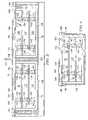
- FIG. 1illustrates a PCB with different types of packages mounted to its surface
- FIGS. 2 a - 2 dillustrate further detail of the semiconductor packages mounted to the PCB
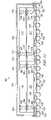
- FIGS. 3 a - 3 jillustrate a process of forming a shielding layer over stacked semiconductor die interconnected by conductive via
- FIG. 4illustrates a face-to-back ISM covered by a shielding layer and interconnected by conductive via
- FIG. 5illustrates an ISM covered by a shielding layer in PiP arrangement
- FIG. 6illustrates an ISM covered by a shielding layer in Fi-PoP arrangement
- FIG. 7illustrates an ISM covered by a shielding layer and interconnected by conductive via
- FIG. 8illustrates a back-to-back ISM covered by a shielding layer and interconnected by conductive via
- FIG. 9illustrates a face-to-face ISM covered by a shielding layer and interconnected by conductive via
- FIG. 10illustrates an ISM covered by a shielding layer and interconnected by conductive via extending through stacked die
- FIG. 11illustrates an ISM of differing size die covered by a shielding layer and interconnected by conductive via
- FIG. 12illustrates an ISM with side-by-side stacked semiconductor die covered by a shielding layer and interconnected by conductive via;
- FIG. 13illustrates an ISM covered by a shielding layer which is connected to a conductive via.
- Front-end manufacturinggenerally refers to formation of the semiconductor devices on the wafer.
- the finished waferhas an active side containing the transistors and other active and passive components.
- Back-end manufacturingrefers to cutting or singulating the finished wafer into the individual die and then packaging the die for structural support and/or environmental isolation.
- a semiconductor wafergenerally includes an active surface having semiconductor devices disposed thereon, and a backside surface formed with bulk semiconductor material, e.g., silicon.
- the active side surfacecontains a plurality of semiconductor die.
- the active surfaceis formed by a variety of semiconductor processes, including layering, patterning, doping, and heat treatment.
- semiconductor materialsare grown or deposited on the substrate by techniques involving thermal oxidation, nitridation, chemical vapor deposition, evaporation, and sputtering.
- Photolithographyinvolves the masking of areas of the surface and etching away undesired material to form specific structures.
- the doping processinjects concentrations of dopant material by thermal diffusion or ion implantation.
- FIG. 1illustrates electronic device 10 having a chip carrier substrate or printed circuit board (PCB) 12 with a plurality of semiconductor packages or semiconductor die mounted on its surface.
- Electronic device 10may have one type of semiconductor package, or multiple types of semiconductor packages, depending on the application. The different types of semiconductor packages are shown in FIG. 1 for purposes of illustration.
- Electronic device 10may be a stand-alone system that uses the semiconductor packages to perform an electrical function. Alternatively, electronic device 10 may be a subcomponent of a larger system. For example, electronic device 10 may be a graphics card, network interface card, or other signal processing card that can be inserted into a computer.
- the semiconductor packagecan include microprocessors, memories, application specific integrated circuits (ASICs), logic circuits, analog circuits, radio frequency (RF) circuits, discrete devices, or other semiconductor die or electrical components.
- ASICsapplication specific integrated circuits
- RFradio frequency
- PCB 12provides a general substrate for structural support and electrical interconnect of the semiconductor packages and other electronic components mounted on the PCB.
- Conductive signal traces 14are formed on a surface or within layers of PCB 12 using evaporation, electrolytic plating, electroless plating, screen printing, or other suitable metal deposition process. Signal traces 14 provide for electrical communication between each of the semiconductor packages, mounted components, and any connected external system components. Traces 14 also provide power and ground connections to each of the semiconductor packages.
- semiconductor packagesincluding a dual in-line package (DIP) 16 , wire-bonded die 18 , bump chip carrier (BCC) 20 , and flip-chip package 22 .
- DIPdual in-line package
- BCCbump chip carrier
- flip-chip package 22any combination of semiconductor packages or other electronic components can be connected to PCB 12 .
- electronic device 10includes a single attached semiconductor package, while other embodiments call for multiple interconnected packages.
- manufacturerscan incorporate pre-made components into electronic devices and systems. Because the semiconductor packages include sophisticated functionality and represent known good units (KGUs), electronic devices can be manufactured using cheaper components and shorten manufacturing process. The resulting devices are less likely to fail and less expensive to manufacture resulting in lower costs for consumers.
- KGUsknown good units
- FIG. 2 aillustrates further detail of DIP 16 mounted on PCB 12 .
- DIP 16includes semiconductor die 24 having contact pads 26 .
- Semiconductor die 24includes an active area containing analog or digital circuits implemented as active devices, passive devices, conductive layers, and dielectric layers formed within semiconductor die 24 and are electrically interconnected according to the electrical design of the die.
- the circuitmay include one or more transistors, diodes, inductors, capacitors, resistors, and other circuit elements formed within the active area of die 24 .
- Contact pads 26are made with a conductive material such as aluminum (Al), copper (Cu), tin (Sn), nickel (Ni), gold (Au), or silver (Ag), and are electrically connected to the circuit elements formed within die 24 .
- Contact pads 26are formed by a physical vapor deposition (PVD), chemical vapor deposition (CVD), electrolytic plating, or electroless plating process.
- PVDphysical vapor deposition
- CVDchemical vapor deposition
- electrolytic platingelectroless plating process.
- semiconductor die 24is mounted to a die attach area of lower portion 28 of the package body using a gold-silicon eutectic layer or adhesive material, such as thermal epoxy.
- the package bodyincludes an insulative packaging material such as plastic or ceramic.
- Conductor leads 30are connected to lower portion 28 of the body and bond wires 32 are formed between leads 30 and contact pads 26 of die 24 .
- Encapsulant 34is deposited over the package for environmental protection by preventing moisture and particles from entering the package and contaminating die 24 , contact pads 26 , or bond wires 32 .
- DIP 16is connected to PCB 12 by inserting leads 30 into holes formed through PCB 12 .
- Solder material 36is flowed around leads 30 and into the holes to physically and electrically connect DIP 16 to PCB 12 .
- Solder material 36can be any metal or electrically conductive material, e.g., Sn, lead (Pb), Au, Ag, Cu, zinc (Zn), bismuthinite (Bi), and alloys thereof, with an optional flux material.
- the solder materialcan be eutectic Sn/Pb, high lead, or lead free.
- a wire-bonded die 18 having contact pads 38is mounted to PCB 12 using adhesive material 40 .
- Contact pads 42are formed on the surface of PCB 12 and electrically connect to one or more traces 14 formed on or within the layers of PCB 12 .
- Bond wires 44are formed between contact pads 38 of die 18 and contact pads 42 of PCB 12 .
- FIG. 2 cillustrates further detail of BCC 20 with an incorporated semiconductor die, integrated circuit (IC), or combination thereof.
- Semiconductor die 46 having contact pads 48is mounted over a carrier using an underfill or epoxy-resin adhesive material 50 .
- Semiconductor die 46includes an active area containing analog or digital circuits implemented as active devices, passive devices, conductive layers, and dielectric layers formed within semiconductor die 46 and are electrically interconnected according to the electrical design of the die.
- the circuitmay include one or more transistors, diodes, inductors, capacitors, resistors, and other circuit elements formed within the active area of die 46 .
- Contact pads 48are connected to the electrical devices and circuitry formed within the active area of die 46 .
- Bond wires 54 and bond pads 56 and 58electrically connect contact pads 48 of die 46 to contact pads 52 of BCC 20 .
- Mold compound or encapsulant 60is deposited over die 46 , bond wires 54 and contact pads 52 to provide physical support and electrical insulation for the device.
- Contact pads 64are formed on PCB 12 and electrically connect to one or more conductive signal traces 14 .
- Solder materialis deposited between contact pads 52 of BCC 20 and contact pads 64 of PCB 12 . The solder material is reflowed to form bumps 66 which form a mechanical and electrical connection between BCC 20 and PCB 12 .
- flip chip style semiconductor device 22has a semiconductor die 72 with active area 70 mounted face down toward PCB 12 .
- Active area 70containing analog or digital circuits implemented as active devices, passive devices, conductive layers, and dielectric layers formed within semiconductor die 72 is electrically interconnected according to the electrical design of the die.
- the circuitmay include one or more transistors, diodes, inductors, capacitors, resistors, and other circuit elements formed within active area 70 of die 72 .
- the electrical and mechanical interconnectis achieved through solder bump structure 76 comprising a large number of individual conductive solder bumps or balls 78 .
- the solder bumpsare formed on bump pads or interconnect sites 80 , which are disposed on active area 70 .
- the bump pads 80connect to the active circuits by conduction tracks in active area 70 .
- the solder bumps 78are electrically and mechanically connected to contact pads or interconnect sites 82 on PCB 12 by a solder reflow process.
- the interconnect sites 82are electrically connected to one or more conductive signal traces 14 on PCB 12 .
- the flip chip semiconductor deviceprovides a short electrical conduction path from the active devices on die 72 to conduction tracks on PCB 12 in order to reduce signal propagation distance, lower capacitance, and achieve overall better circuit performance.
- a plurality of semiconductor dieis formed on a semiconductor wafer 90 using conventional integrated circuit processes, as described above.
- the semiconductor wafer, containing semiconductor die 94 and 100is mounted to expansion table 92 with ultraviolet (UV) tape.
- the backside of semiconductor die 94is affixed to expansion table or carrier 92 with its front side, i.e., active surface 96 and contact pads 98 , oriented face up.
- the backside of semiconductor die 100is mounted to expansion table 92 with its front side, i.e., active surface 102 and contact pads 104 , oriented face up.
- a conductive through silicon via (TSV) 110is disposed under and electrically connected to contact pads 98 .
- a conductive TSV 112is disposed under and electrically connected to contact pads 104 .
- the conductive TSVsare formed by drilling or etching a hole through the silicon and depositing a conductive material in the hole. More generally, the conductive via 110 can be formed through any semiconductor material including gallium arsenide and germanium.
- a saw street 108is disposed between semiconductor die 94 and 100 .
- FIG. 3 bshows an embodiment with additional semiconductor wafers, each containing semiconductor die with conductive TSVs for electrical interconnection, stacked over semiconductor wafer 90 .
- This configurationprovides for stacking multiple semiconductor die within the shielding layer as described below.
- a semiconductor wafer 114is disposed on semiconductor wafer 90 .
- Semiconductor wafer 114is configured similar to wafer 90 including semiconductor die 116 having conductive TSV 118 disposed under and electrically connected to contacts pads on the active surface of die 116 .
- Semiconductor die 124includes conductive TSV 126 disposed under and electrically connected to contacts pads on the active surface of die 124 .
- TSVs 118 and 126electrically connect to contact pads 98 and 104 , respectively, with bonding agents 128 , such as conductive adhesive, metal-to-metal bonding, or other suitable electrically conductive union.
- a semiconductor wafer 130is disposed on semiconductor wafer 114 .
- Semiconductor wafer 130is configured similar to wafer 90 including semiconductor die 132 having conductive TSV 134 disposed under and electrically connected to contacts pads on the active surface of die 132 .
- Semiconductor die 138includes conductive TSV 140 disposed under and electrically connected to contacts pads on the active surface of die 138 .
- TSVs 134 and 140electrically connect to the contact pads of semiconductor die 116 and 124 with bonding agents 142 , such as conductive adhesive, metal-to-metal bonding, or other suitable electrically conductive union.
- bonding agents 142such as conductive adhesive, metal-to-metal bonding, or other suitable electrically conductive union.
- semiconductor die 94 , 116 , and 132are aligned to enable interconnection of the conductive TSVs.
- semiconductor die 100 , 124 , and 138are aligned to enable interconnection of the conductive TSVs.
- An adhesive or underfill material 143is disposed between the stacked semiconductor wafers.
- a saw blade or laser tool 144cuts through saw street 108 of semiconductor wafers 90 , 114 , and 130 in a dicing operation.
- expansion table 92moves in two-dimension lateral directions, as shown by arrows 146 , to expand the width of saw street 108 , i.e., form a gap and create a greater physical separation between the die.
- Expansion table 92moves substantially the same distance in the x-axis and y-axis to provide equal separation around a periphery of each die.
- the post-expansion width of gap 108ranges from 5 micrometers ( ⁇ m) to 200 ⁇ m.
- the expanded gap 108defines a peripheral region around the semiconductor die.
- the semiconductor waferis diced to separate the semiconductor die.
- the individual semiconductor dieare then transferred and affixed to a temporary chip carrier with an adhesive layer, e.g., thermal epoxy.
- the semiconductor dieare placed on the chip carrier so as to have a predetermined separation gap.
- the separation gaphas sufficient width to form a shielding layer within the gap, as described below.
- Semiconductor die 94 , 100 , 116 , 124 , 132 , and 138may contain baseband circuits that are susceptible to electromagnetic interference (EMI), radio frequency interference (RFI), and other inter-device interference.
- semiconductor die 94 , 100 , 116 , 124 , 132 , and 138may contain integrated passive devices (IPD) that generate EMI or RFI.
- IPDs contained within semiconductor die 94 , 100 , 116 , 124 , 132 , and 138provide the electrical characteristics needed for high frequency applications, such as high-pass filters, low-pass filters, band-pass filters, symmetric Hi-Q resonant transformers, and tuning capacitors.
- a typical RF systemrequires multiple IPDs in one or more semiconductor packages to perform the necessary electrical functions.
- IPDsgenerate undesired EMI, RFI, or other inter-device interference, such as capacitive, inductive, or conductive coupling, also known as cross-talk, which can interfere with the operation of adjacent circuit elements.
- the interferencecan be generated internally or originate from external semiconductor devices containing IPDs or RF circuits. In any case, the EMI and RFI radiation should be blocked to avoid adversely influencing the operation of adjacent devices.
- a conductive material 148is formed on expansion table 92 a predetermined distance from the adjacent semiconductor die.
- conductive material 148rings around each semiconductor die in a bottom portion of gap 108 .
- conductive material 148is disposed in specific areas in a bottom portion of gap 108 between the semiconductor die.
- Conductive material 148is a stiffener ring or slot made with conductive epoxy, polymers, Al, Cu, Sn, Ni, Au, Ag, or other suitable conductive material. In one embodiment, stiffener ring 148 is placed at least 1 ⁇ m from the adjacent semiconductor die.
- an organic insulating material 150is deposited in gap 108 and over semiconductor die 94 , 100 , 116 , 124 , 132 , and 138 using spin coating, needle dispensing, or other suitable application process.
- Organic material 150completely covers and encloses all sides of the semiconductor die above expansion table 92 .
- Organic material 150can be BCB, PI, or acrylic resin.
- other non-conductive materialssuch as a polymer molding compound, liquid epoxy molding, compression molding, soft laminating film, or other material having dielectric or electrical insulating properties can be deposited in gap 108 .
- the non-conductive materialscan also be deposited using a transfer molding or injection molding process.
- Organic material 150completely covers semiconductor die 94 , 100 , 116 , 124 , 132 , and 138 and stiffener ring 148 above expansion table 92 .
- a portion of organic material 150is removed by etching or laser drilling to stiffener ring 148 .
- the removal of organic material 150forms recesses 152 and exposes stiffener ring 148 .
- the walls of recess 152can be vertical or tapered.
- a tapered surface 154is cut into stiffener ring 148 .
- an electrically conductive material 158is conformally deposited in recesses 152 with an optional seed layer.
- Conductive material 158completely covers and encloses all sides of semiconductor die 94 , 100 , 116 , 124 , 132 , and 138 above expansion table 92 to provide shielding for the semiconductor die against EMI, RFI, or other inter-device interference.
- Conductive material 158electrically connects to stiffener ring 148 .
- Conductive material 158can be Cu, Al, stainless steel, nickel silver, low-carbon steel, silicon-iron steel, and other metals and composites capable of blocking EMI, RFI, and other inter-device interference.
- the seed layercan be made with Cu, Ni, nickel vanadium (NiV), Au, or Al.
- the seed layer and conductive material 158are patterned and conformally deposited using an electrolytic plating, electroless plating, sputtering, PVD, CVD, or other suitable metal deposition process.
- the assemblyis inverted and attached to wafer carrier 160 using UV or thermal release adhesive.
- the assemblyis then removed from expansion table 92 .
- a substrate 162 with build-up interconnect layers and structures 164 and 166is formed on the backside of semiconductor die 94 and 100 .
- Substrate 162is typically built up layer-by-layer with corresponding lamination, deposition, and plating processes. Accordingly, substrate 162 includes contact pads, conduction channels, redistribution layers, and insulating layers as determined by the electrical design of the semiconductor device. In particular, contact pads 166 electrically connect to stiffener ring 148 .
- one or more contact pads 166are electrically connected through a conduction channel in substrate 162 to one or more contact pads 164 , which in turn electrically connect to an external low-impedance ground point to aid the shielding feature of conductive material 158 .
- the wafer expansion technology in FIG. 3 dcan be used to reduce production time.
- shielding layer 158is formed over all semiconductor die 94 , 100 , 116 , 124 , 132 , and 138 at the same time to save manufacturing steps and cost.
- Semiconductor wafers 90 , 114 , and 130are singulated in FIG. 3 j through a center portion of gap 108 , i.e., between recesses 152 .
- the gap regionis cut by a cutting tool 168 such as a saw blade or laser.
- the cutting toolcompletely severs the semiconductor wafers through the gap region to separate the die.
- FIG. 4shows stacked semiconductor die 94 , 116 , and 132 as an internal stacking module (ISM) following wafer singulation with conformal shielding layer 158 covering the ISM.
- the shielding layer 158provides advantages over conventional shielding cages.
- the wafer-level shieldingis simultaneously formed over all semiconductor die in the ISM after creating recesses 152 to expose stiffener ring 148 .
- the shielding layerprovides isolation for the ISM with respect to EMI, RFI, or other inter-device interference.
- the build-up interconnect layers 162 - 166are formed on the stacked semiconductor die.
- the ground path for shielding layer 158includes stiffener ring 148 and grounded contact pads 164 and 166 . Grounding shield layer 158 improves its shielding effectiveness.
- the build-up interconnection layer like 162 - 166can be formed after encapsulation in FIG. 3 f .
- the stacked wafersare transferred to another carrier to form recessed sections like 152 on a periphery of the semiconductor die.
- the shielding layer like 158is then formed over all semiconductor die simultaneously, followed by singulation of the stacked wafers.
- FIG. 5illustrates the ISM from FIG. 4 in a package-in-package (PiP) configuration.
- ISM 170includes stacked semiconductor die 172 , 174 , and 176 with interconnecting conductive TSV 178 , 180 , and 182 , respectively.
- TSVs 178electrically connect to TSVs 180 through bonding agent 184 .
- TSVs 180electrically connect to TSVs 182 through bonding agent 186 .
- Shielding layer 188covers semiconductor die 172 - 176 .
- a substrate 190 with build-up interconnect structure 192is formed on the backside of semiconductor die 172 .
- Shielding layer 188electrically connects to build-up interconnect structure 192 through stiffener ring 189 .
- ISM 170is attached to flip chip type semiconductor die or other semiconductor package 194 with adhesive material 196 .
- Solder bumps 198are formed on contact pads of semiconductor die 194 to electrically connect the flip chip semiconductor device to interconnect structures 200 on PCB 202 .
- the ISM 170also electrically connects to interconnect structures 200 in PCB 202 by way of bond wires 204 .
- Solder bumps 206are formed on interconnect structure 200 to provide external connectivity for the PiP device.
- the electrical conduction path for shielding layer 188 to an external ground pointincludes stiffener ring 189 , interconnect structure 192 , bond wire 204 , interconnect structure 200 , and solder bumps 206 .
- a molding compound or encapsulant 208is deposited over ISM 170 and bond wires 204 and PCB 202 .
- Molding compound 208can be made with epoxy acrylate or other polymer material and applied by transfer molding, liquid encapsulant molding, or other molding process. Molding compound 208 is non-conductive and environmentally protects the semiconductor device from external elements and contaminants.
- semiconductor die 172 - 176are memory devices and semiconductor die 194 contains RF circuits.
- Shielding layer 188blocks EMI, RFI, or other interference generated by die 194 from adversely influencing the operation of die 172 - 176 .
- FIG. 6illustrates the ISM from FIG. 4 in a fan-in package-on-package (Fi-PoP) configuration.
- the ISM 210includes stacked semiconductor die 212 , 214 , and 216 with interconnecting conductive TSV 218 , 220 , and 222 , respectively.
- TSVs 218electrically connect to TSVs 220 through bonding agent 224 .
- TSVs 220electrically connect to TSVs 222 through bonding agent 226 .
- Shielding layer 228covers semiconductor die 212 - 216 .
- a substrate 230 with build-up interconnect structure 232is formed on the backside of semiconductor die 212 .
- Shielding layer 228electrically connects to build-up interconnect structure 232 through stiffener ring 229 .
- the ISM 210is attached to flip chip type semiconductor die or other semiconductor package 234 with adhesive material 236 .
- Solder bumps 238are formed on contact pads of semiconductor die 234 to electrically connect the flip chip semiconductor device to interconnect structures 240 on PCB 242 .
- the ISM 210also electrically connects to interconnect structures 240 in PCB 242 by way of bond wires 244 .
- Solder bumps 246are formed on interconnect structure 240 to provide external connectivity for the Fi-PoP device.
- the electrical conduction path for shielding layer 228 to an external ground pointincludes stiffener ring 229 , interconnect structure 232 , bond wire 244 , interconnect structure 240 , and solder bumps 246 .
- a molding compound or encapsulant 248is deposited over ISM 210 and bond wires 244 and PCB 242 .
- Molding compound 248can be made with epoxy acrylate or other polymer material and applied by transfer molding, liquid encapsulant molding, or other molding process. Molding compound 248 is non-conductive and environmentally protects the semiconductor device from external elements and contaminants.
- a cavityis formed in encapsulant 248 by a contour molding process to expose substrate 230 and interconnect structure 232 .
- Semiconductor package 250includes semiconductor die 252 mounted to PCB 254 .
- Semiconductor die 252electrically connects to interconnect structure 256 in PCB 254 with bond wires 258 .
- An encapsulant 260is formed over semiconductor die 250 and bond wires 258 and PCB 254 .
- the interconnect structure 256 of PCB 254electrically connects to substrate 230 and interconnect structure 232 with solder bumps 264 .
- semiconductor die 212 - 216are memory devices and semiconductor die 234 contains RF circuits.
- Semiconductor die 252contains a logic control circuit for the memory.
- Shielding layer 228blocks EMI, RFI, or other interference generated by die 234 from adversely influencing the operation of die 212 - 216 and 252 .
- FIG. 7illustrates ISM 270 with semiconductor die in a face-to-back arrangement.
- Semiconductor die 272includes contact pads 274 formed on its active surface. Contact pads 274 are electrically connected through conductive layer 276 to conductive vias 278 .
- Conductive layer 276is patterned and deposited on semiconductor die 272 using an evaporation, electrolytic plating, electroless plating, or other suitable metal deposition process. Conductive layer 276 can be made with Al, Cu, Sn, Ni, Au, Ag, or other suitable conductive material.
- Conductive vias 278are formed in organic material 280 around a periphery of semiconductor die 272 .
- the movement of expansion table 92 in FIG. 3 dcreates a separation gap of sufficient width to form conductive vias within the gap.
- An organic insulating materialis deposited in the gap using spin coating, needle dispensing, or other suitable application process.
- the organic materialcan be BCB, PI, or acrylic resin.
- other non-conductive materialssuch as a polymer molding compound, liquid epoxy molding, compression molding, soft laminating film, or other material having dielectric or electrical insulating properties can be deposited in the gap.
- the non-conductive materialscan also be deposited using a transfer molding or injection molding process. A portion of the organic material is removed by laser drilling or etching to create through hole vias (THV) extending down to expansion table 92 .
- TSVthrough hole vias
- An electrically conductive materialis deposited in the THVs with an optional seed layer.
- the conductive materialcan be Al, Cu, Sn, Ni, Au, or Ag.
- the seed layercan be made with Cu, Ni, NiV, Au, or Al.
- the seed layer and conductive materialare patterned and deposited using an electrolytic plating, electroless plating, sputtering, PVD, CVD, or other suitable metal deposition process.
- the semiconductor waferis singulated with a cutting tool, such as a saw blade or laser, through the organic material, or through the conductive material in the THVs.
- the conductive material in the THVsforms conductive vias 278 extending through organic material 280 from one side of semiconductor die 272 to the other side of the die.
- Semiconductor die 282includes contact pads 284 formed on its active surface. Contact pads 284 are electrically connected through conductive layer 286 to conductive THVs 288 .
- the conductive THVs 288are formed in organic material 290 around a periphery of semiconductor die 282 , similar to conductive THVs 278 .
- THVs 288electrically connect to THVs 278 through bonding agent 289 .
- Semiconductor die 292includes contact pads 294 formed on its active surface. Contact pads 294 are electrically connected through conductive layer 296 to conductive THVs 298 .
- the conductive THVs 298are formed in organic material 300 around a periphery of semiconductor die 292 , similar to conductive THVs 278 .
- THVs 298electrically connect to THVs 288 through bonding agent 299 .
- Organic insulating material 302is deposited over stacked semiconductor die 272 , 282 , and 292 .
- Shielding layer 304conformally covers stacked semiconductor die 272 , 282 , and 292 and electrically connects to stiffener ring 306 .
- Shielding layer 304isolates the semiconductor die with respect to EMI, RFI, and other inter-device interference.
- PCB 308is formed on ISM 270 with a build-up process that includes interconnect structure 310 .
- Solder bumps 312are formed on interconnect structure 310 to provide external connectivity for ISM 270 .
- Shielding layer 304is electrically connected through the portion of interconnect structure 310 connected to stiffener ring 306 and through one or more solder bumps 312 which are connected to an external ground point to improve its shielding effectiveness.
- FIG. 8illustrates ISM 320 with semiconductor die in a back-to-back arrangement.
- Semiconductor die 322includes contact pads 324 formed on its active surface. Contact pads 324 are electrically connected to conductive TSVs 326 , see FIG. 3 a .
- Semiconductor die 332includes contact pads 334 formed on its active surface. Contact pads 334 are electrically connected to conductive TSVs 336 .
- Conductive TSVs 326electrically connect to conductive TSVs 336 with bonding agent 338 .
- Organic insulating material 340is deposited over stacked semiconductor die 322 and 332 . Shielding layer 342 conformally covers stacked semiconductor die 322 and 332 and electrically connects to stiffener ring 344 .
- Shielding layer 342isolates the semiconductor die with respect to EMI, RFI, and other inter-device interference.
- PCB 348is formed on ISM 320 with a build-up process that includes interconnect structure 350 .
- Solder bumps 352are formed on interconnect structure 350 to provide external connectivity for ISM 320 .
- Shielding layer 342is electrically connected through the portion of interconnect structure 350 connected to stiffener ring 344 and through one or more solder bumps 352 which are connected to an external ground point to improve its shielding effectiveness.
- FIG. 9illustrates ISM 360 with semiconductor die in a face-to-face arrangement.
- Semiconductor die 362includes contact pads 364 formed on its active surface. Contact pads 364 are electrically connected to conductive TSVs 366 , see FIG. 3 a .
- Semiconductor die 372includes contact pads 374 formed on its active surface. Contact pads 374 are electrically connected to conductive TSVs 376 . Contact pads 374 electrically connect to contact pads 364 with bonding agent 378 .
- Organic insulating material 380is deposited over stacked semiconductor die 362 and 372 .
- Shielding layer 382conformally covers stacked semiconductor die 362 and 372 and electrically connects to stiffener ring 384 .
- Shielding layer 382isolates the semiconductor die with respect to EMI, RFI, and other inter-device interference.
- PCB 388is formed on ISM 360 with a build-up process that includes interconnect structure 390 .
- Solder bumps 392are formed on interconnect structure 390 to provide external connectivity for ISM 360 .
- Shielding layer 382is electrically connected through the portion of interconnect structure 390 connected to stiffener ring 384 and through one or more solder bumps 392 which are connected to an external ground point to improve its shielding effectiveness.
- FIG. 10illustrates ISM 400 with semiconductor die in a face-to-back arrangement.
- Semiconductor die 402includes contact pads 404 formed on its active surface.
- Semiconductor die 406includes contact pads 408 formed on its active surface.
- Semiconductor die 410includes contact pads 412 formed on its active surface.
- Conductive TSVs 414extend through stacked semiconductor die 402 , 406 , and 410 and electrically connect contact pads 404 , 408 , and 412 .
- Each conductive TSV 414extends through all stacked semiconductor die 402 , 406 , and 410 .
- Organic insulating material 416is deposited over stacked semiconductor die 402 , 406 , and 410 .
- Shielding layer 418conformally covers stacked semiconductor die 402 , 406 , and 410 and electrically connects to stiffener ring 420 . Shielding layer 418 isolates the semiconductor die with respect to EMI, RFI, and other inter-device interference.
- PCB 422is formed on ISM 400 with a build-up process that includes interconnect structure 424 . Solder bumps 426 are formed on interconnect structure 424 to provide external connectivity for ISM 400 .
- Shielding layer 418is electrically connected through the portion of interconnect structure 424 connected to stiffener ring 420 and through one or more solder bumps 426 which are connected to an external ground point to improve its shielding effectiveness.
- FIG. 11illustrates ISM 430 with semiconductor die in a face-to-back arrangement.
- Semiconductor die 432includes contact pads 434 formed on its active surface. Contact pads 434 are electrically connected through conductive layer 436 to conductive vias 438 .
- Conductive layer 436is patterned and deposited on semiconductor die 432 using an evaporation, electrolytic plating, electroless plating, or other suitable metal deposition process. Conductive layer 436 can be made with Al, Cu, Sn, Ni, Au, Ag, or other suitable conductive material.
- the conductive vias 438are formed in organic material 440 around a periphery of semiconductor die 432 .
- the movement of expansion table 92 in FIG. 3 dcreates a separation gap of sufficient width to form conductive vias within the gap.
- An organic insulating materialis deposited in the gap using spin coating, needle dispensing, or other suitable application process.
- the organic materialcan be BCB, PI, or acrylic resin.
- other non-conductive materialssuch as a polymer molding compound, liquid epoxy molding, compression molding, soft laminating film, or other material having dielectric or electrical insulating properties can be deposited in the gap.
- the non-conductive materialscan also be deposited using a transfer molding or injection molding process. A portion of the organic material is removed by laser drilling or etching to create THVs extending down to expansion table 92 .
- An electrically conductive materialis deposited in the THVs with an optional seed layer.
- the conductive materialcan be Al, Cu, Sn, Ni, Au, or Ag.
- the seed layercan be made with Cu, Ni, NiV, Au, or Al.
- the seed layer and conductive materialare patterned and deposited using an electrolytic plating, electroless plating, sputtering, PVD, CVD, or other suitable metal deposition process.
- the semiconductor waferis singulated with a cutting tool, such as a saw blade or laser, through the organic material, or through the conductive material in the THVs.
- the conductive material in the THVsforms conductive vias 438 extending through organic material 440 from one side of semiconductor die 432 to the other side of the die.
- Semiconductor die 442includes contact pads 444 formed on its active surface. Contact pads 444 are electrically connected through conductive layer 446 to conductive THVs 448 .
- the conductive THVs 448are formed in organic material 450 around a periphery of semiconductor die 442 , similar to conductive THVs 438 .
- THVs 448electrically connect to THVs 438 through bonding agent 449 .
- Semiconductor die 452includes contact pads 454 formed on its active surface. Contact pads 454 are electrically connected through conductive layer 456 to conductive THVs 458 .
- the conductive THVs 458are formed in organic material 460 around a periphery of semiconductor die 452 , similar to conductive THVs 438 .
- THVs 458electrically connect to THVs 448 through bonding agent 459 .
- Semiconductor die 432 , 442 , and 452differ in size, i.e., die 442 is smaller than die 432 or 452 .
- Organic insulating material 462is deposited over stacked semiconductor die 432 , 442 , and 452 .
- Shielding layer 464conformally covers stacked semiconductor die 432 , 442 , and 452 and electrically connects to stiffener ring 466 .
- Shielding layer 464isolates the semiconductor die with respect to EMI, RFI, and other inter-device interference.
- PCB 468is formed on ISM 430 with a build-up process that includes interconnect structure 470 .
- Solder bumps 472are formed on interconnect structure 470 to provide external connectivity for ISM 430 .
- Shielding layer 464is electrically connected through the portion of interconnect structure 470 connected to stiffener ring 466 and through one or more solder bumps 472 which are connected to an external ground point to improve its shielding effectiveness.
- FIG. 12illustrates ISM 480 with semiconductor die in a face-to-back arrangement.
- Semiconductor die 482includes contact pads 484 formed on its active surface. Contact pads 484 are electrically connected to conductive TSVs 486 , see FIG. 3 a .
- Semiconductor die 492includes contact pads 494 formed on its active surface. Contact pads 494 are electrically connected to conductive TSVs 496 . Conductive TSVs 486 electrically connect to conductive TSVs 496 with bonding agent 498 .
- Semiconductor die 502includes contact pads 504 formed on its active surface. Contact pads 504 are electrically connected to conductive TSVs 506 , see FIG. 3 a .
- Semiconductor die 512includes contact pads 514 formed on its active surface.
- Conductive TSVs 516electrically connect to conductive TSVs 506 with bonding agent 518 .
- Conductive layer 520is patterned and deposited on semiconductor die 482 and 502 using an evaporation, electrolytic plating, electroless plating, or other suitable metal deposition process. Conductive layer 520 can be made with Al, Cu, Sn, Ni, Au, Ag, or other suitable conductive material.
- Organic insulating material 522is deposited over stacked semiconductor die 482 , 492 , 502 , and 512 .
- Shielding layer 524conformally covers stacked semiconductor die 482 , 492 , 502 , and 512 and electrically connects to stiffener ring 526 .
- Shielding layer 524isolates the semiconductor die with respect to EMI, RFI, and other inter-device interference.
- PCB 528is formed on ISM 480 with a build-up process that includes interconnect structure 530 .
- Solder bumps 532are formed on interconnect structure 530 to provide external connectivity for ISM 480 .
- Shielding layer 524is electrically connected through the portion of interconnect structure 530 connected to stiffener ring 526 and through one or more solder bumps 532 which are connected to an external ground point to improve its shielding effectiveness.
- FIG. 13illustrates ISM 540 with semiconductor die in a face-to-back arrangement.
- Semiconductor die 542includes contact pads 544 formed on its active surface. Contact pads 544 are electrically connected to conductive TSVs 546 , see FIG. 3 a .
- Semiconductor die 552includes contact pads 554 formed on its active surface. Contact pads 554 are electrically connected to conductive TSVs 556 .
- Conductive TSVs 546electrically connect to conductive TSVs 556 with bonding agent 558 .
- Semiconductor die 562includes contact pads 564 formed on its active surface. Contact pads 564 are electrically connected to conductive TSVs 566 .
- Conductive TSVs 556electrically connect to conductive TSVs 566 with bonding agent 568 .
- Organic insulating material 570is deposited over stacked semiconductor die 542 , 552 , and 562 .
- Shielding layer 572conformally covers stacked semiconductor die 542 , 552 , and 562 and electrically connects to stiffener ring 576 .
- Shielding layer 572isolates the semiconductor die with respect to EMI, RFI, and other inter-device interference.
- Shielding layer 572also electrically connects to TSV 544 of semiconductor die 542 with conduction channel or bonding agent 578 .
- PCB 580is formed on ISM 540 with a build-up process that includes interconnect structure 582 .
- Solder bumps 584are formed on interconnect structure 530 to provide external connectivity for ISM 540 .
- Shielding layer 572is electrically connected through the portion of interconnect structure 582 connected to stiffener ring 576 and through one or more solder bumps 584 which are connected to an external ground point to improve its shielding effectiveness.
Landscapes
- Engineering & Computer Science (AREA)
- Microelectronics & Electronic Packaging (AREA)
- Power Engineering (AREA)
- Computer Hardware Design (AREA)
- Physics & Mathematics (AREA)
- Condensed Matter Physics & Semiconductors (AREA)
- General Physics & Mathematics (AREA)
- Manufacturing & Machinery (AREA)
- Toxicology (AREA)
- Electromagnetism (AREA)
- Health & Medical Sciences (AREA)
- Internal Circuitry In Semiconductor Integrated Circuit Devices (AREA)
- Semiconductor Integrated Circuits (AREA)
Abstract
Description
- The present invention relates in general to semiconductor devices and, more particularly, to a semiconductor device having a shielding layer for isolation with respect to electromagnetic interference, radio frequency interference, and other inter-device interference.
- Semiconductor devices are found in many products in the fields of entertainment, communications, networks, computers, and household markets. Semiconductor devices are also found in military, aviation, automotive, industrial controllers, and office equipment. The semiconductor devices perform a variety of electrical functions necessary for each of these applications.
- The manufacture of semiconductor devices involves formation of a wafer having a plurality of die. Each semiconductor die contains hundreds or thousands of transistors and other active and passive devices performing a variety of electrical functions. For a given wafer, each die from the wafer typically performs the same electrical function. Front-end manufacturing generally refers to formation of the semiconductor devices on the wafer. The finished wafer has an active side containing the transistors and other active and passive components. Back-end manufacturing refers to cutting or singulating the finished wafer into the individual die and then packaging the die for structural support and environmental isolation.
- One goal of semiconductor manufacturing is to produce a package suitable for faster, reliable, smaller, and higher-density integrated circuits (IC) at lower cost. Flip chip packages or wafer level chip scale packages (WLCSP) are ideally suited for ICs demanding high speed, high density, and greater pin count. Flip chip style packaging involves mounting the active side of the die face down toward a chip carrier substrate or printed circuit board (PCB). The electrical and mechanical interconnect between the active devices on the die and conduction tracks on the carrier substrate is achieved through a solder bump structure comprising a large number of conductive solder bumps or balls. The solder bumps are formed by a reflow process applied to solder material deposited on contact pads, which are disposed on the semiconductor substrate. The solder bumps are then soldered to the carrier substrate. The flip chip semiconductor package provides a short electrical conduction path from the active devices on the die to the carrier substrate in order to reduce signal propagation, lower capacitance, and achieve overall better circuit performance.
- In many applications, it is desirable to vertically stack semiconductor die for greater device integration and minimize interconnect routing. The electrical interconnection between stacked semiconductor die has been done by using through hole vias which traverse from a front side to the backside of the die. The through hole vias are formed by drilling through the active area of the die or through saw streets on the wafer prior to any dicing operation. The through hole vias are filled with conductive material. The process of drilling through hole vias in the active area of the die or in saw streets on the wafer can cause damage to the wafer and/or die.
- In high frequency applications, such as radio frequency (RF) wireless communications, integrated passive devices (IPDs) are often contained within the semiconductor device. Examples of IPDs include resistors, capacitors, and inductors. A typical RF system requires multiple IPDs in one or more semiconductor packages to perform the necessary electrical functions. However, most IPDs generate undesired electromagnetic interference (EMI) and radio frequency interference (RFI), or other inter-device interference, such as capacitive, inductive, or conductive coupling, also known as cross-talk, which can interfere with the operation of adjacent circuit elements.
- Various attempts have been made to shield the semiconductor devices from undesirable EMI and RFI by using metal enclosures, e.g., Faraday cage. However, encasing each stacked semiconductor device increases the total size of the package due to the space taken by the cage. The time required to mount a shielding cage on every stacked device increases manufacturing costs and reduces productivity.
- A need exists to shield semiconductor die from EMI, RFI, and other inter-device interference. Accordingly, in one embodiment, the present invention is a method of making a semiconductor device comprising the steps of providing a first semiconductor wafer having a plurality of semiconductor die, creating a gap between the semiconductor die, depositing a conductive material in a bottom portion of the gap, depositing an insulating material in the gap and over the semiconductor die, removing a portion of the insulating material in the gap to form a recess between each semiconductor die extending to the conductive material, and forming a shielding layer over the insulating material and in the recess to contact the conductive material. The shielding layer isolates the semiconductor die from inter-device interference. The method further includes the steps of forming a substrate with a build-up structure on the semiconductor die adjacent to the conductive material, electrically connecting the conductive material to a ground point in the substrate, and singulating the first semiconductor wafer through the gap to separate the semiconductor die.
- In another embodiment, the present invention is a method of making a semiconductor device comprising the steps of providing a first semiconductor wafer having a plurality of semiconductor die, disposing a second semiconductor wafer having a plurality of semiconductor die over the first semiconductor wafer so that the semiconductor die in the first and second wafers are aligned, creating a gap between the semiconductor die of the first and second semiconductor wafers, depositing a conductive material in a bottom portion of the gap, depositing an insulating material in the gap and over the semiconductor die of the first and second semiconductor wafers, removing a portion of the insulating material in the gap to form a recess between each semiconductor die extending to the conductive material, and forming a shielding layer over the insulating material and in the recess to contact the conductive material. The shielding layer isolates the semiconductor die from inter-device interference. The method further includes the step of singulating the first and second semiconductor wafers through the gap to separate the semiconductor die.
- In another embodiment, the present invention is a method of making a semiconductor device comprising the steps of creating a gap between a plurality of semiconductor die, depositing a conductive material in a bottom portion of the gap, depositing an insulating material in the gap and over the semiconductor die, removing a portion of the insulating material in the gap to form a recess between each semiconductor die extending to the conductive material, and forming a shielding layer over the insulating material and in the recess to contact the conductive material. The shielding layer isolates the semiconductor die from inter-device interference.
- In another embodiment, the present invention is a semiconductor device comprising a semiconductor die including a conductive via. A stiffener ring is formed around the semiconductor die. An insulating layer is formed over the semiconductor die. A shielding layer is formed over the insulating material to isolate the semiconductor die from inter-device interference. The shielding layer electrically connects to the stiffener ring. A substrate is attached to the semiconductor die. The stiffener ring is electrically connected to a ground point in the substrate.
FIG. 1 illustrates a PCB with different types of packages mounted to its surface;FIGS. 2 a-2dillustrate further detail of the semiconductor packages mounted to the PCB;FIGS. 3 a-3jillustrate a process of forming a shielding layer over stacked semiconductor die interconnected by conductive via;FIG. 4 illustrates a face-to-back ISM covered by a shielding layer and interconnected by conductive via;FIG. 5 illustrates an ISM covered by a shielding layer in PiP arrangement;FIG. 6 illustrates an ISM covered by a shielding layer in Fi-PoP arrangement;FIG. 7 illustrates an ISM covered by a shielding layer and interconnected by conductive via;FIG. 8 illustrates a back-to-back ISM covered by a shielding layer and interconnected by conductive via;FIG. 9 illustrates a face-to-face ISM covered by a shielding layer and interconnected by conductive via;FIG. 10 illustrates an ISM covered by a shielding layer and interconnected by conductive via extending through stacked die;FIG. 11 illustrates an ISM of differing size die covered by a shielding layer and interconnected by conductive via;FIG. 12 illustrates an ISM with side-by-side stacked semiconductor die covered by a shielding layer and interconnected by conductive via; andFIG. 13 illustrates an ISM covered by a shielding layer which is connected to a conductive via.- The present invention is described in one or more embodiments in the following description with reference to the Figures, in which like numerals represent the same or similar elements. While the invention is described in terms of the best mode for achieving the invention's objectives, it will be appreciated by those skilled in the art that it is intended to cover alternatives, modifications, and equivalents as may be included within the spirit and scope of the invention as defined by the appended claims and their equivalents as supported by the following disclosure and drawings.
- The manufacture of semiconductor devices involves formation of a wafer having a plurality of die. Each die contains hundreds or thousands of transistors and other active and passive devices performing one or more electrical functions. For a given wafer, each die from the wafer typically performs the same electrical function. Front-end manufacturing generally refers to formation of the semiconductor devices on the wafer. The finished wafer has an active side containing the transistors and other active and passive components. Back-end manufacturing refers to cutting or singulating the finished wafer into the individual die and then packaging the die for structural support and/or environmental isolation.
- A semiconductor wafer generally includes an active surface having semiconductor devices disposed thereon, and a backside surface formed with bulk semiconductor material, e.g., silicon. The active side surface contains a plurality of semiconductor die. The active surface is formed by a variety of semiconductor processes, including layering, patterning, doping, and heat treatment. In the layering process, semiconductor materials are grown or deposited on the substrate by techniques involving thermal oxidation, nitridation, chemical vapor deposition, evaporation, and sputtering. Photolithography involves the masking of areas of the surface and etching away undesired material to form specific structures. The doping process injects concentrations of dopant material by thermal diffusion or ion implantation.
FIG. 1 illustrateselectronic device 10 having a chip carrier substrate or printed circuit board (PCB)12 with a plurality of semiconductor packages or semiconductor die mounted on its surface.Electronic device 10 may have one type of semiconductor package, or multiple types of semiconductor packages, depending on the application. The different types of semiconductor packages are shown inFIG. 1 for purposes of illustration.Electronic device 10 may be a stand-alone system that uses the semiconductor packages to perform an electrical function. Alternatively,electronic device 10 may be a subcomponent of a larger system. For example,electronic device 10 may be a graphics card, network interface card, or other signal processing card that can be inserted into a computer.- The semiconductor package can include microprocessors, memories, application specific integrated circuits (ASICs), logic circuits, analog circuits, radio frequency (RF) circuits, discrete devices, or other semiconductor die or electrical components.
- In
FIG. 1 ,PCB 12 provides a general substrate for structural support and electrical interconnect of the semiconductor packages and other electronic components mounted on the PCB. Conductive signal traces14 are formed on a surface or within layers ofPCB 12 using evaporation, electrolytic plating, electroless plating, screen printing, or other suitable metal deposition process. Signal traces14 provide for electrical communication between each of the semiconductor packages, mounted components, and any connected external system components.Traces 14 also provide power and ground connections to each of the semiconductor packages. - For the purpose of illustration, several types of semiconductor packages, including a dual in-line package (DIP)16, wire-bonded
die 18, bump chip carrier (BCC)20, and flip-chip package 22, are shown mounted onPCB 12. Depending upon the system requirements, any combination of semiconductor packages or other electronic components can be connected toPCB 12. In some embodiments,electronic device 10 includes a single attached semiconductor package, while other embodiments call for multiple interconnected packages. By combining one or more semiconductor packages over a single substrate, manufacturers can incorporate pre-made components into electronic devices and systems. Because the semiconductor packages include sophisticated functionality and represent known good units (KGUs), electronic devices can be manufactured using cheaper components and shorten manufacturing process. The resulting devices are less likely to fail and less expensive to manufacture resulting in lower costs for consumers. FIG. 2 aillustrates further detail ofDIP 16 mounted onPCB 12.DIP 16 includes semiconductor die24 havingcontact pads 26. Semiconductor die24 includes an active area containing analog or digital circuits implemented as active devices, passive devices, conductive layers, and dielectric layers formed within semiconductor die24 and are electrically interconnected according to the electrical design of the die. For example, the circuit may include one or more transistors, diodes, inductors, capacitors, resistors, and other circuit elements formed within the active area ofdie 24. Contactpads 26 are made with a conductive material such as aluminum (Al), copper (Cu), tin (Sn), nickel (Ni), gold (Au), or silver (Ag), and are electrically connected to the circuit elements formed withindie 24. Contactpads 26 are formed by a physical vapor deposition (PVD), chemical vapor deposition (CVD), electrolytic plating, or electroless plating process. During assembly ofDIP 16, semiconductor die24 is mounted to a die attach area oflower portion 28 of the package body using a gold-silicon eutectic layer or adhesive material, such as thermal epoxy. The package body includes an insulative packaging material such as plastic or ceramic. Conductor leads30 are connected tolower portion 28 of the body andbond wires 32 are formed betweenleads 30 andcontact pads 26 ofdie 24.Encapsulant 34 is deposited over the package for environmental protection by preventing moisture and particles from entering the package and contaminatingdie 24,contact pads 26, orbond wires 32.DIP 16 is connected toPCB 12 by insertingleads 30 into holes formed throughPCB 12.Solder material 36 is flowed around leads30 and into the holes to physically and electrically connectDIP 16 toPCB 12.Solder material 36 can be any metal or electrically conductive material, e.g., Sn, lead (Pb), Au, Ag, Cu, zinc (Zn), bismuthinite (Bi), and alloys thereof, with an optional flux material. For example, the solder material can be eutectic Sn/Pb, high lead, or lead free.- Referring to
FIG. 2 b, a wire-bondeddie 18 havingcontact pads 38 is mounted toPCB 12 usingadhesive material 40. Contactpads 42 are formed on the surface ofPCB 12 and electrically connect to one ormore traces 14 formed on or within the layers ofPCB 12.Bond wires 44 are formed betweencontact pads 38 ofdie 18 andcontact pads 42 ofPCB 12. FIG. 2 cillustrates further detail ofBCC 20 with an incorporated semiconductor die, integrated circuit (IC), or combination thereof. Semiconductor die46 havingcontact pads 48 is mounted over a carrier using an underfill or epoxy-resin adhesive material 50. Semiconductor die46 includes an active area containing analog or digital circuits implemented as active devices, passive devices, conductive layers, and dielectric layers formed within semiconductor die46 and are electrically interconnected according to the electrical design of the die. For example, the circuit may include one or more transistors, diodes, inductors, capacitors, resistors, and other circuit elements formed within the active area ofdie 46. Contactpads 48 are connected to the electrical devices and circuitry formed within the active area ofdie 46.Bond wires 54 andbond pads contact pads 48 ofdie 46 to contactpads 52 ofBCC 20. Mold compound orencapsulant 60 is deposited overdie 46,bond wires 54 andcontact pads 52 to provide physical support and electrical insulation for the device. Contactpads 64 are formed onPCB 12 and electrically connect to one or more conductive signal traces14. Solder material is deposited betweencontact pads 52 ofBCC 20 andcontact pads 64 ofPCB 12. The solder material is reflowed to formbumps 66 which form a mechanical and electrical connection betweenBCC 20 andPCB 12.- In
FIG. 2 d, flip chipstyle semiconductor device 22 has asemiconductor die 72 withactive area 70 mounted face down towardPCB 12.Active area 70 containing analog or digital circuits implemented as active devices, passive devices, conductive layers, and dielectric layers formed within semiconductor die72 is electrically interconnected according to the electrical design of the die. For example, the circuit may include one or more transistors, diodes, inductors, capacitors, resistors, and other circuit elements formed withinactive area 70 ofdie 72. The electrical and mechanical interconnect is achieved throughsolder bump structure 76 comprising a large number of individual conductive solder bumps orballs 78. The solder bumps are formed on bump pads orinterconnect sites 80, which are disposed onactive area 70. Thebump pads 80 connect to the active circuits by conduction tracks inactive area 70. The solder bumps78 are electrically and mechanically connected to contact pads orinterconnect sites 82 onPCB 12 by a solder reflow process. Theinterconnect sites 82 are electrically connected to one or more conductive signal traces14 onPCB 12. The flip chip semiconductor device provides a short electrical conduction path from the active devices on die72 to conduction tracks onPCB 12 in order to reduce signal propagation distance, lower capacitance, and achieve overall better circuit performance. - Turning to
FIG. 3 a, a plurality of semiconductor die is formed on asemiconductor wafer 90 using conventional integrated circuit processes, as described above. The semiconductor wafer, containing semiconductor die94 and100, is mounted to expansion table92 with ultraviolet (UV) tape. The backside of semiconductor die94 is affixed to expansion table orcarrier 92 with its front side, i.e.,active surface 96 andcontact pads 98, oriented face up. Likewise, the backside of semiconductor die100 is mounted to expansion table92 with its front side, i.e.,active surface 102 andcontact pads 104, oriented face up. Contactpads active areas pads 98. Aconductive TSV 112 is disposed under and electrically connected to contactpads 104. The conductive TSVs are formed by drilling or etching a hole through the silicon and depositing a conductive material in the hole. More generally, the conductive via110 can be formed through any semiconductor material including gallium arsenide and germanium. Asaw street 108 is disposed between semiconductor die94 and100. FIG. 3 bshows an embodiment with additional semiconductor wafers, each containing semiconductor die with conductive TSVs for electrical interconnection, stacked oversemiconductor wafer 90. This configuration provides for stacking multiple semiconductor die within the shielding layer as described below. For example, asemiconductor wafer 114 is disposed onsemiconductor wafer 90.Semiconductor wafer 114 is configured similar towafer 90 including semiconductor die116 havingconductive TSV 118 disposed under and electrically connected to contacts pads on the active surface ofdie 116. Semiconductor die124 includesconductive TSV 126 disposed under and electrically connected to contacts pads on the active surface ofdie 124.TSVs pads bonding agents 128, such as conductive adhesive, metal-to-metal bonding, or other suitable electrically conductive union. Asemiconductor wafer 130 is disposed onsemiconductor wafer 114.Semiconductor wafer 130 is configured similar towafer 90 including semiconductor die132 havingconductive TSV 134 disposed under and electrically connected to contacts pads on the active surface ofdie 132. Semiconductor die138 includesconductive TSV 140 disposed under and electrically connected to contacts pads on the active surface ofdie 138.TSVs bonding agents 142, such as conductive adhesive, metal-to-metal bonding, or other suitable electrically conductive union. In stackingsemiconductor wafers underfill material 143 is disposed between the stacked semiconductor wafers.- In
FIG. 3 c, a saw blade orlaser tool 144 cuts throughsaw street 108 ofsemiconductor wafers FIG. 3 d, expansion table92 moves in two-dimension lateral directions, as shown byarrows 146, to expand the width ofsaw street 108, i.e., form a gap and create a greater physical separation between the die. Expansion table92 moves substantially the same distance in the x-axis and y-axis to provide equal separation around a periphery of each die. The post-expansion width ofgap 108 ranges from 5 micrometers (μm) to 200 μm. The expandedgap 108 defines a peripheral region around the semiconductor die. - In an alternate embodiment, the semiconductor wafer is diced to separate the semiconductor die. The individual semiconductor die are then transferred and affixed to a temporary chip carrier with an adhesive layer, e.g., thermal epoxy. The semiconductor die are placed on the chip carrier so as to have a predetermined separation gap. In general, the separation gap has sufficient width to form a shielding layer within the gap, as described below.
- Semiconductor die94,100,116,124,132, and138 may contain baseband circuits that are susceptible to electromagnetic interference (EMI), radio frequency interference (RFI), and other inter-device interference. In other embodiments, semiconductor die94,100,116,124,132, and138 may contain integrated passive devices (IPD) that generate EMI or RFI. For example, the IPDs contained within semiconductor die94,100,116,124,132, and138 provide the electrical characteristics needed for high frequency applications, such as high-pass filters, low-pass filters, band-pass filters, symmetric Hi-Q resonant transformers, and tuning capacitors. A typical RF system requires multiple IPDs in one or more semiconductor packages to perform the necessary electrical functions. However, most IPDs generate undesired EMI, RFI, or other inter-device interference, such as capacitive, inductive, or conductive coupling, also known as cross-talk, which can interfere with the operation of adjacent circuit elements. The interference can be generated internally or originate from external semiconductor devices containing IPDs or RF circuits. In any case, the EMI and RFI radiation should be blocked to avoid adversely influencing the operation of adjacent devices.
- In
FIG. 3 e, aconductive material 148 is formed on expansion table92 a predetermined distance from the adjacent semiconductor die. In one embodiment,conductive material 148 rings around each semiconductor die in a bottom portion ofgap 108. Alternatively,conductive material 148 is disposed in specific areas in a bottom portion ofgap 108 between the semiconductor die.Conductive material 148 is a stiffener ring or slot made with conductive epoxy, polymers, Al, Cu, Sn, Ni, Au, Ag, or other suitable conductive material. In one embodiment,stiffener ring 148 is placed at least 1 μm from the adjacent semiconductor die. - In
FIG. 3 f, an organic insulatingmaterial 150 is deposited ingap 108 and over semiconductor die94,100,116,124,132, and138 using spin coating, needle dispensing, or other suitable application process.Organic material 150 completely covers and encloses all sides of the semiconductor die above expansion table92.Organic material 150 can be BCB, PI, or acrylic resin. Alternatively, other non-conductive materials such as a polymer molding compound, liquid epoxy molding, compression molding, soft laminating film, or other material having dielectric or electrical insulating properties can be deposited ingap 108. The non-conductive materials can also be deposited using a transfer molding or injection molding process.Organic material 150 completely covers semiconductor die94,100,116,124,132, and138 andstiffener ring 148 above expansion table92. - In
FIG. 3 g, a portion oforganic material 150 is removed by etching or laser drilling tostiffener ring 148. The removal oforganic material 150 forms recesses152 and exposesstiffener ring 148. The walls ofrecess 152 can be vertical or tapered. Atapered surface 154 is cut intostiffener ring 148. - In
FIG. 3 h, an electricallyconductive material 158 is conformally deposited inrecesses 152 with an optional seed layer.Conductive material 158 completely covers and encloses all sides of semiconductor die94,100,116,124,132, and138 above expansion table92 to provide shielding for the semiconductor die against EMI, RFI, or other inter-device interference.Conductive material 158 electrically connects to stiffenerring 148.Conductive material 158 can be Cu, Al, stainless steel, nickel silver, low-carbon steel, silicon-iron steel, and other metals and composites capable of blocking EMI, RFI, and other inter-device interference. The seed layer can be made with Cu, Ni, nickel vanadium (NiV), Au, or Al. The seed layer andconductive material 158 are patterned and conformally deposited using an electrolytic plating, electroless plating, sputtering, PVD, CVD, or other suitable metal deposition process. - In
FIG. 3 i, the assembly is inverted and attached towafer carrier 160 using UV or thermal release adhesive. The assembly is then removed from expansion table92. Asubstrate 162 with build-up interconnect layers andstructures Substrate 162 is typically built up layer-by-layer with corresponding lamination, deposition, and plating processes. Accordingly,substrate 162 includes contact pads, conduction channels, redistribution layers, and insulating layers as determined by the electrical design of the semiconductor device. In particular,contact pads 166 electrically connect tostiffener ring 148. As part of the substrate build-up interconnect structure, one ormore contact pads 166 are electrically connected through a conduction channel insubstrate 162 to one ormore contact pads 164, which in turn electrically connect to an external low-impedance ground point to aid the shielding feature ofconductive material 158. By stacking semiconductor die94,100,116,124,132, and138 prior to forming interconnect structures162-164, the wafer expansion technology inFIG. 3 dcan be used to reduce production time. In addition, shieldinglayer 158 is formed over all semiconductor die94,100,116,124,132, and138 at the same time to save manufacturing steps and cost.Semiconductor wafers FIG. 3 jthrough a center portion ofgap 108, i.e., betweenrecesses 152. The gap region is cut by acutting tool 168 such as a saw blade or laser. The cutting tool completely severs the semiconductor wafers through the gap region to separate the die. - The stacked semiconductor die are removed from
carrier 160.FIG. 4 shows stacked semiconductor die94,116, and132 as an internal stacking module (ISM) following wafer singulation withconformal shielding layer 158 covering the ISM. Theshielding layer 158 provides advantages over conventional shielding cages. The wafer-level shielding is simultaneously formed over all semiconductor die in the ISM after creatingrecesses 152 to exposestiffener ring 148. The shielding layer provides isolation for the ISM with respect to EMI, RFI, or other inter-device interference. The build-up interconnect layers162-166 are formed on the stacked semiconductor die. The ground path for shieldinglayer 158 includesstiffener ring 148 and groundedcontact pads shield layer 158 improves its shielding effectiveness. - In an alternate process, the build-up interconnection layer like162-166 can be formed after encapsulation in
FIG. 3 f. The stacked wafers are transferred to another carrier to form recessed sections like152 on a periphery of the semiconductor die. The shielding layer like158 is then formed over all semiconductor die simultaneously, followed by singulation of the stacked wafers. FIG. 5 illustrates the ISM fromFIG. 4 in a package-in-package (PiP) configuration.ISM 170 includes stacked semiconductor die172,174, and176 with interconnectingconductive TSV TSVs 178 electrically connect toTSVs 180 throughbonding agent 184.TSVs 180 electrically connect toTSVs 182 throughbonding agent 186.Shielding layer 188 covers semiconductor die172-176. Asubstrate 190 with build-upinterconnect structure 192 is formed on the backside of semiconductor die172.Shielding layer 188 electrically connects to build-upinterconnect structure 192 throughstiffener ring 189.ISM 170 is attached to flip chip type semiconductor die orother semiconductor package 194 withadhesive material 196. Solder bumps198 are formed on contact pads of semiconductor die194 to electrically connect the flip chip semiconductor device to interconnectstructures 200 onPCB 202. TheISM 170 also electrically connects to interconnectstructures 200 inPCB 202 by way ofbond wires 204. Solder bumps206 are formed oninterconnect structure 200 to provide external connectivity for the PiP device. In particular, the electrical conduction path for shieldinglayer 188 to an external ground point includesstiffener ring 189,interconnect structure 192,bond wire 204,interconnect structure 200, and solder bumps206.- A molding compound or
encapsulant 208 is deposited overISM 170 andbond wires 204 andPCB 202.Molding compound 208 can be made with epoxy acrylate or other polymer material and applied by transfer molding, liquid encapsulant molding, or other molding process.Molding compound 208 is non-conductive and environmentally protects the semiconductor device from external elements and contaminants. - In one PiP embodiment, semiconductor die172-176 are memory devices and semiconductor die194 contains RF circuits.
Shielding layer 188 blocks EMI, RFI, or other interference generated bydie 194 from adversely influencing the operation of die172-176. FIG. 6 illustrates the ISM fromFIG. 4 in a fan-in package-on-package (Fi-PoP) configuration. TheISM 210 includes stacked semiconductor die212,214, and216 with interconnectingconductive TSV TSVs 218 electrically connect toTSVs 220 throughbonding agent 224.TSVs 220 electrically connect toTSVs 222 throughbonding agent 226.Shielding layer 228 covers semiconductor die212-216. Asubstrate 230 with build-upinterconnect structure 232 is formed on the backside of semiconductor die212.Shielding layer 228 electrically connects to build-upinterconnect structure 232 throughstiffener ring 229. TheISM 210 is attached to flip chip type semiconductor die orother semiconductor package 234 withadhesive material 236. Solder bumps238 are formed on contact pads of semiconductor die234 to electrically connect the flip chip semiconductor device to interconnectstructures 240 onPCB 242. TheISM 210 also electrically connects to interconnectstructures 240 inPCB 242 by way ofbond wires 244. Solder bumps246 are formed oninterconnect structure 240 to provide external connectivity for the Fi-PoP device. In particular, the electrical conduction path for shieldinglayer 228 to an external ground point includesstiffener ring 229,interconnect structure 232,bond wire 244,interconnect structure 240, and solder bumps246.- A molding compound or
encapsulant 248 is deposited overISM 210 andbond wires 244 andPCB 242.Molding compound 248 can be made with epoxy acrylate or other polymer material and applied by transfer molding, liquid encapsulant molding, or other molding process.Molding compound 248 is non-conductive and environmentally protects the semiconductor device from external elements and contaminants. A cavity is formed inencapsulant 248 by a contour molding process to exposesubstrate 230 andinterconnect structure 232.Semiconductor package 250 includes semiconductor die252 mounted toPCB 254. Semiconductor die252 electrically connects to interconnectstructure 256 inPCB 254 withbond wires 258. Anencapsulant 260 is formed over semiconductor die250 andbond wires 258 andPCB 254. Theinterconnect structure 256 ofPCB 254 electrically connects tosubstrate 230 andinterconnect structure 232 with solder bumps264. - In one Fi-PoP embodiment, semiconductor die212-216 are memory devices and semiconductor die234 contains RF circuits. Semiconductor die252 contains a logic control circuit for the memory.
Shielding layer 228 blocks EMI, RFI, or other interference generated bydie 234 from adversely influencing the operation of die212-216 and252. FIG. 7 illustratesISM 270 with semiconductor die in a face-to-back arrangement. Semiconductor die272 includescontact pads 274 formed on its active surface. Contactpads 274 are electrically connected throughconductive layer 276 toconductive vias 278.Conductive layer 276 is patterned and deposited on semiconductor die272 using an evaporation, electrolytic plating, electroless plating, or other suitable metal deposition process.Conductive layer 276 can be made with Al, Cu, Sn, Ni, Au, Ag, or other suitable conductive material.Conductive vias 278 are formed inorganic material 280 around a periphery of semiconductor die272.- To form
conductive vias 278, the movement of expansion table92 inFIG. 3 dcreates a separation gap of sufficient width to form conductive vias within the gap. An organic insulating material is deposited in the gap using spin coating, needle dispensing, or other suitable application process. The organic material can be BCB, PI, or acrylic resin. Alternatively, other non-conductive materials such as a polymer molding compound, liquid epoxy molding, compression molding, soft laminating film, or other material having dielectric or electrical insulating properties can be deposited in the gap. The non-conductive materials can also be deposited using a transfer molding or injection molding process. A portion of the organic material is removed by laser drilling or etching to create through hole vias (THV) extending down to expansion table92. An electrically conductive material is deposited in the THVs with an optional seed layer. The conductive material can be Al, Cu, Sn, Ni, Au, or Ag. The seed layer can be made with Cu, Ni, NiV, Au, or Al. The seed layer and conductive material are patterned and deposited using an electrolytic plating, electroless plating, sputtering, PVD, CVD, or other suitable metal deposition process. The semiconductor wafer is singulated with a cutting tool, such as a saw blade or laser, through the organic material, or through the conductive material in the THVs. The conductive material in the THVs formsconductive vias 278 extending throughorganic material 280 from one side of semiconductor die272 to the other side of the die. - Semiconductor die282 includes
contact pads 284 formed on its active surface. Contactpads 284 are electrically connected throughconductive layer 286 toconductive THVs 288. Theconductive THVs 288 are formed inorganic material 290 around a periphery of semiconductor die282, similar toconductive THVs 278.THVs 288 electrically connect to THVs278 throughbonding agent 289. Semiconductor die292 includescontact pads 294 formed on its active surface. Contactpads 294 are electrically connected throughconductive layer 296 toconductive THVs 298. Theconductive THVs 298 are formed inorganic material 300 around a periphery of semiconductor die292, similar toconductive THVs 278.THVs 298 electrically connect to THVs288 throughbonding agent 299. Organic insulatingmaterial 302 is deposited over stacked semiconductor die272,282, and292.Shielding layer 304 conformally covers stacked semiconductor die272,282, and292 and electrically connects to stiffenerring 306.Shielding layer 304 isolates the semiconductor die with respect to EMI, RFI, and other inter-device interference.PCB 308 is formed onISM 270 with a build-up process that includesinterconnect structure 310. Solder bumps312 are formed oninterconnect structure 310 to provide external connectivity forISM 270.Shielding layer 304 is electrically connected through the portion ofinterconnect structure 310 connected tostiffener ring 306 and through one or more solder bumps312 which are connected to an external ground point to improve its shielding effectiveness. FIG. 8 illustratesISM 320 with semiconductor die in a back-to-back arrangement. Semiconductor die322 includescontact pads 324 formed on its active surface. Contactpads 324 are electrically connected toconductive TSVs 326, seeFIG. 3 a. Semiconductor die332 includescontact pads 334 formed on its active surface. Contactpads 334 are electrically connected toconductive TSVs 336.Conductive TSVs 326 electrically connect toconductive TSVs 336 withbonding agent 338. Organic insulatingmaterial 340 is deposited over stacked semiconductor die322 and332.Shielding layer 342 conformally covers stacked semiconductor die322 and332 and electrically connects to stiffenerring 344.Shielding layer 342 isolates the semiconductor die with respect to EMI, RFI, and other inter-device interference.PCB 348 is formed onISM 320 with a build-up process that includesinterconnect structure 350. Solder bumps352 are formed oninterconnect structure 350 to provide external connectivity forISM 320.Shielding layer 342 is electrically connected through the portion ofinterconnect structure 350 connected tostiffener ring 344 and through one or more solder bumps352 which are connected to an external ground point to improve its shielding effectiveness.FIG. 9 illustratesISM 360 with semiconductor die in a face-to-face arrangement. Semiconductor die362 includescontact pads 364 formed on its active surface. Contactpads 364 are electrically connected toconductive TSVs 366, seeFIG. 3 a. Semiconductor die372 includescontact pads 374 formed on its active surface. Contactpads 374 are electrically connected toconductive TSVs 376. Contactpads 374 electrically connect to contactpads 364 withbonding agent 378. Organic insulatingmaterial 380 is deposited over stacked semiconductor die362 and372.Shielding layer 382 conformally covers stacked semiconductor die362 and372 and electrically connects to stiffenerring 384.Shielding layer 382 isolates the semiconductor die with respect to EMI, RFI, and other inter-device interference.PCB 388 is formed onISM 360 with a build-up process that includesinterconnect structure 390. Solder bumps392 are formed oninterconnect structure 390 to provide external connectivity forISM 360.Shielding layer 382 is electrically connected through the portion ofinterconnect structure 390 connected tostiffener ring 384 and through one or more solder bumps392 which are connected to an external ground point to improve its shielding effectiveness.FIG. 10 illustratesISM 400 with semiconductor die in a face-to-back arrangement. Semiconductor die402 includescontact pads 404 formed on its active surface. Semiconductor die406 includescontact pads 408 formed on its active surface. Semiconductor die410 includescontact pads 412 formed on its active surface.Conductive TSVs 414 extend through stacked semiconductor die402,406, and410 and electrically connectcontact pads conductive TSV 414 extends through all stacked semiconductor die402,406, and410. Organic insulatingmaterial 416 is deposited over stacked semiconductor die402,406, and410.Shielding layer 418 conformally covers stacked semiconductor die402,406, and410 and electrically connects to stiffenerring 420.Shielding layer 418 isolates the semiconductor die with respect to EMI, RFI, and other inter-device interference.PCB 422 is formed onISM 400 with a build-up process that includesinterconnect structure 424. Solder bumps426 are formed oninterconnect structure 424 to provide external connectivity forISM 400.Shielding layer 418 is electrically connected through the portion ofinterconnect structure 424 connected tostiffener ring 420 and through one or more solder bumps426 which are connected to an external ground point to improve its shielding effectiveness.FIG. 11 illustratesISM 430 with semiconductor die in a face-to-back arrangement. Semiconductor die432 includescontact pads 434 formed on its active surface. Contactpads 434 are electrically connected throughconductive layer 436 toconductive vias 438.Conductive layer 436 is patterned and deposited on semiconductor die432 using an evaporation, electrolytic plating, electroless plating, or other suitable metal deposition process.Conductive layer 436 can be made with Al, Cu, Sn, Ni, Au, Ag, or other suitable conductive material. Theconductive vias 438 are formed inorganic material 440 around a periphery of semiconductor die432.- To form
conductive vias 438, the movement of expansion table92 inFIG. 3 dcreates a separation gap of sufficient width to form conductive vias within the gap. An organic insulating material is deposited in the gap using spin coating, needle dispensing, or other suitable application process. The organic material can be BCB, PI, or acrylic resin. Alternatively, other non-conductive materials such as a polymer molding compound, liquid epoxy molding, compression molding, soft laminating film, or other material having dielectric or electrical insulating properties can be deposited in the gap. The non-conductive materials can also be deposited using a transfer molding or injection molding process. A portion of the organic material is removed by laser drilling or etching to create THVs extending down to expansion table92. An electrically conductive material is deposited in the THVs with an optional seed layer. The conductive material can be Al, Cu, Sn, Ni, Au, or Ag. The seed layer can be made with Cu, Ni, NiV, Au, or Al. The seed layer and conductive material are patterned and deposited using an electrolytic plating, electroless plating, sputtering, PVD, CVD, or other suitable metal deposition process. The semiconductor wafer is singulated with a cutting tool, such as a saw blade or laser, through the organic material, or through the conductive material in the THVs. The conductive material in the THVs formsconductive vias 438 extending throughorganic material 440 from one side of semiconductor die432 to the other side of the die. - Semiconductor die442 includes
contact pads 444 formed on its active surface. Contactpads 444 are electrically connected throughconductive layer 446 toconductive THVs 448. Theconductive THVs 448 are formed inorganic material 450 around a periphery of semiconductor die442, similar toconductive THVs 438.THVs 448 electrically connect to THVs438 throughbonding agent 449. Semiconductor die452 includescontact pads 454 formed on its active surface. Contactpads 454 are electrically connected throughconductive layer 456 toconductive THVs 458. Theconductive THVs 458 are formed inorganic material 460 around a periphery of semiconductor die452, similar toconductive THVs 438.THVs 458 electrically connect to THVs448 throughbonding agent 459. Semiconductor die432,442, and452 differ in size, i.e., die442 is smaller than die432 or452. Organic insulatingmaterial 462 is deposited over stacked semiconductor die432,442, and452.Shielding layer 464 conformally covers stacked semiconductor die432,442, and452 and electrically connects to stiffenerring 466.Shielding layer 464 isolates the semiconductor die with respect to EMI, RFI, and other inter-device interference.PCB 468 is formed onISM 430 with a build-up process that includesinterconnect structure 470. Solder bumps472 are formed oninterconnect structure 470 to provide external connectivity forISM 430.Shielding layer 464 is electrically connected through the portion ofinterconnect structure 470 connected tostiffener ring 466 and through one or more solder bumps472 which are connected to an external ground point to improve its shielding effectiveness. FIG. 12 illustratesISM 480 with semiconductor die in a face-to-back arrangement. Semiconductor die482 includescontact pads 484 formed on its active surface. Contactpads 484 are electrically connected toconductive TSVs 486, seeFIG. 3 a. Semiconductor die492 includescontact pads 494 formed on its active surface. Contactpads 494 are electrically connected toconductive TSVs 496.Conductive TSVs 486 electrically connect toconductive TSVs 496 withbonding agent 498. Semiconductor die502 includescontact pads 504 formed on its active surface. Contactpads 504 are electrically connected toconductive TSVs 506, seeFIG. 3 a. Semiconductor die512 includescontact pads 514 formed on its active surface. Contactpads 514 are electrically connected toconductive TSVs 516.Conductive TSVs 516 electrically connect toconductive TSVs 506 withbonding agent 518.Conductive layer 520 is patterned and deposited on semiconductor die482 and502 using an evaporation, electrolytic plating, electroless plating, or other suitable metal deposition process.Conductive layer 520 can be made with Al, Cu, Sn, Ni, Au, Ag, or other suitable conductive material. Organic insulatingmaterial 522 is deposited over stacked semiconductor die482,492,502, and512.Shielding layer 524 conformally covers stacked semiconductor die482,492,502, and512 and electrically connects to stiffenerring 526.Shielding layer 524 isolates the semiconductor die with respect to EMI, RFI, and other inter-device interference.PCB 528 is formed onISM 480 with a build-up process that includesinterconnect structure 530. Solder bumps532 are formed oninterconnect structure 530 to provide external connectivity forISM 480.Shielding layer 524 is electrically connected through the portion ofinterconnect structure 530 connected tostiffener ring 526 and through one or more solder bumps532 which are connected to an external ground point to improve its shielding effectiveness.FIG. 13 illustratesISM 540 with semiconductor die in a face-to-back arrangement. Semiconductor die542 includescontact pads 544 formed on its active surface. Contactpads 544 are electrically connected toconductive TSVs 546, seeFIG. 3 a. Semiconductor die552 includescontact pads 554 formed on its active surface. Contactpads 554 are electrically connected toconductive TSVs 556.Conductive TSVs 546 electrically connect toconductive TSVs 556 withbonding agent 558. Semiconductor die562 includescontact pads 564 formed on its active surface. Contactpads 564 are electrically connected toconductive TSVs 566.Conductive TSVs 556 electrically connect toconductive TSVs 566 withbonding agent 568. Organic insulatingmaterial 570 is deposited over stacked semiconductor die542,552, and562.Shielding layer 572 conformally covers stacked semiconductor die542,552, and562 and electrically connects to stiffenerring 576.Shielding layer 572 isolates the semiconductor die with respect to EMI, RFI, and other inter-device interference.Shielding layer 572 also electrically connects to TSV544 of semiconductor die542 with conduction channel orbonding agent 578.PCB 580 is formed onISM 540 with a build-up process that includesinterconnect structure 582. Solder bumps584 are formed oninterconnect structure 530 to provide external connectivity forISM 540.Shielding layer 572 is electrically connected through the portion ofinterconnect structure 582 connected tostiffener ring 576 and through one or more solder bumps584 which are connected to an external ground point to improve its shielding effectiveness.- While one or more embodiments of the present invention have been illustrated in detail, the skilled artisan will appreciate that modifications and adaptations to those embodiments may be made without departing from the scope of the present invention as set forth in the following claims.
Claims (23)
Priority Applications (2)
| Application Number | Priority Date | Filing Date | Title |
|---|---|---|---|
| US12/133,216US8101460B2 (en) | 2008-06-04 | 2008-06-04 | Semiconductor device and method of shielding semiconductor die from inter-device interference |
| US13/339,185US8648448B2 (en) | 2008-06-04 | 2011-12-28 | Semiconductor device and method of shielding semiconductor die from inter-device interference |
Applications Claiming Priority (1)
| Application Number | Priority Date | Filing Date | Title |
|---|---|---|---|
| US12/133,216US8101460B2 (en) | 2008-06-04 | 2008-06-04 | Semiconductor device and method of shielding semiconductor die from inter-device interference |
Related Child Applications (1)
| Application Number | Title | Priority Date | Filing Date |
|---|---|---|---|
| US13/339,185DivisionUS8648448B2 (en) | 2008-06-04 | 2011-12-28 | Semiconductor device and method of shielding semiconductor die from inter-device interference |
Publications (2)
| Publication Number | Publication Date |
|---|---|
| US20090302435A1true US20090302435A1 (en) | 2009-12-10 |
| US8101460B2 US8101460B2 (en) | 2012-01-24 |
Family
ID=41399553
Family Applications (2)
| Application Number | Title | Priority Date | Filing Date |
|---|---|---|---|
| US12/133,216Active2029-07-16US8101460B2 (en) | 2008-06-04 | 2008-06-04 | Semiconductor device and method of shielding semiconductor die from inter-device interference |
| US13/339,185Active2028-09-11US8648448B2 (en) | 2008-06-04 | 2011-12-28 | Semiconductor device and method of shielding semiconductor die from inter-device interference |
Family Applications After (1)
| Application Number | Title | Priority Date | Filing Date |
|---|---|---|---|
| US13/339,185Active2028-09-11US8648448B2 (en) | 2008-06-04 | 2011-12-28 | Semiconductor device and method of shielding semiconductor die from inter-device interference |
Country Status (1)
| Country | Link |
|---|---|
| US (2) | US8101460B2 (en) |
Cited By (103)
| Publication number | Priority date | Publication date | Assignee | Title |
|---|---|---|---|---|
| US20100001378A1 (en)* | 2008-07-01 | 2010-01-07 | Teledyne Scientific & Imaging, Llc | Through-substrate vias and method of fabricating same |
| US20100044877A1 (en)* | 2008-08-21 | 2010-02-25 | Michael Bruennert | Electronic device having a chip stack |
| US20100065942A1 (en)* | 2008-09-17 | 2010-03-18 | Stats Chippac, Ltd. | Semiconductor Device and Method of Forming High-Frequency Circuit Structure and Method Thereof |
| US20100127345A1 (en)* | 2008-11-25 | 2010-05-27 | Freescale Semiconductor, Inc. | 3-d circuits with integrated passive devices |
| US20100140779A1 (en)* | 2008-12-08 | 2010-06-10 | Stats Chippac, Ltd. | Semiconductor Package with Semiconductor Core Structure and Method of Forming Same |
| US20100140801A1 (en)* | 2008-12-10 | 2010-06-10 | Elpida Memory, Inc. | Device |
| US20100148316A1 (en)* | 2008-12-11 | 2010-06-17 | Stats Chippac, Ltd. | Semiconductor Device and Method of Forming Topside and Bottom-side Interconnect Structures Around Core Die with TSV |
| US20100200965A1 (en)* | 2009-02-11 | 2010-08-12 | Advanced Semiconductor Engineering, Inc. | Package structure for wireless communication module |
| US20100230795A1 (en)* | 2009-03-13 | 2010-09-16 | Tessera Technologies Hungary Kft. | Stacked microelectronic assemblies having vias extending through bond pads |
| US20100244217A1 (en)* | 2009-03-25 | 2010-09-30 | Jong-Woo Ha | Integrated circuit packaging system with stacked configuration and method of manufacture thereof |
| US20100261311A1 (en)* | 2009-04-10 | 2010-10-14 | Elpida Memory, Inc. | Method of manufacturing a semiconductor device |
| US20110006408A1 (en)* | 2009-07-13 | 2011-01-13 | Advanced Semiconductor Engineering, Inc. | Chip package and manufacturing method thereof |
| US20110062592A1 (en)* | 2009-09-11 | 2011-03-17 | Taiwan Semiconductor Manufacturing Company, Ltd. | Delamination Resistance of Stacked Dies in Die Saw |
| US20110121442A1 (en)* | 2009-11-24 | 2011-05-26 | Advanced Semiconductor Engineering, Inc. | Package structure and package process |
| US20110140247A1 (en)* | 2009-12-11 | 2011-06-16 | Reza Argenty Pagaila | Integrated circuit packaging system with shielded package and method of manufacture thereof |
| US20110175215A1 (en)* | 2010-01-19 | 2011-07-21 | International Business Machines Corporation | 3d chip stack having encapsulated chip-in-chip |
| US20110215450A1 (en)* | 2010-03-05 | 2011-09-08 | Chi Heejo | Integrated circuit packaging system with encapsulation and method of manufacture thereof |
| CN102270588A (en)* | 2010-06-02 | 2011-12-07 | 新科金朋有限公司 | Semiconductor device and method of forming emi shielding layer around semiconductor die |
| US8084300B1 (en) | 2010-11-24 | 2011-12-27 | Unisem (Mauritius) Holdings Limited | RF shielding for a singulated laminate semiconductor device package |
| US20120045611A1 (en)* | 2010-08-17 | 2012-02-23 | Taiwan Semiconductor Manufacturing Company, Ltd. | Composite Carrier Structure |
| US20120056312A1 (en)* | 2010-09-02 | 2012-03-08 | Stats Chippac, Ltd. | Semiconductor Device and Method of Forming TSV Semiconductor Wafer with Embedded Semiconductor Die |
| US20120063106A1 (en)* | 2010-09-15 | 2012-03-15 | Young Il Kim | Rf layered module using three dimensional vertical wiring and disposing method thereof |
| US20120074559A1 (en)* | 2010-09-24 | 2012-03-29 | International Business Machines Corporation | Integrated circuit package using through substrate vias to ground lid |
| CN102543969A (en)* | 2010-12-30 | 2012-07-04 | 财团法人工业技术研究院 | Wafer level mold bonding structure and method for manufacturing the same |
| US20120170162A1 (en)* | 2011-01-05 | 2012-07-05 | Siliconware Precision Industries Co., Ltd. | Semiconductor package and fabrication method thereof |
| US20120228749A1 (en)* | 2011-03-08 | 2012-09-13 | Stats Chippac, Ltd. | Semiconductor device and method of forming shielding layer over semiconductor die mounted to tsv interposer |
| US20120292781A1 (en)* | 2011-05-19 | 2012-11-22 | Microsemi Semiconductor Limited | Integrated circuit package |
| US8350367B2 (en) | 2008-02-05 | 2013-01-08 | Advanced Semiconductor Engineering, Inc. | Semiconductor device packages with electromagnetic interference shielding |
| US8368185B2 (en) | 2009-11-19 | 2013-02-05 | Advanced Semiconductor Engineering, Inc. | Semiconductor device packages with electromagnetic interference shielding |
| US20130032952A1 (en)* | 2011-08-01 | 2013-02-07 | Stats Chippac, Ltd. | Semiconductor Device and Method of Forming POP With Stacked Semiconductor Die and Bumps Formed Directly on the Lower Die |
| US8378466B2 (en) | 2009-11-19 | 2013-02-19 | Advanced Semiconductor Engineering, Inc. | Wafer-level semiconductor device packages with electromagnetic interference shielding |
| US8410584B2 (en) | 2008-08-08 | 2013-04-02 | Advanced Semiconductor Engineering, Inc. | Semiconductor device packages with electromagnetic interference shielding |
| EP2579307A1 (en)* | 2011-10-07 | 2013-04-10 | Freescale Semiconductor, Inc. | Stacked semiconductor devices |
| US8471376B1 (en)* | 2009-05-06 | 2013-06-25 | Marvell International Ltd. | Integrated circuit packaging configurations |
| US20130223041A1 (en)* | 2012-02-23 | 2013-08-29 | Apple Inc. | Low profile, space efficient circuit shields |
| US8541883B2 (en) | 2011-11-29 | 2013-09-24 | Advanced Semiconductor Engineering, Inc. | Semiconductor device having shielded conductive vias |
| US8643167B2 (en) | 2011-01-06 | 2014-02-04 | Advanced Semiconductor Engineering, Inc. | Semiconductor package with through silicon vias and method for making the same |
| US8692362B2 (en) | 2010-08-30 | 2014-04-08 | Advanced Semiconductor Engineering, Inc. | Semiconductor structure having conductive vias and method for manufacturing the same |
| US20140146495A1 (en)* | 2010-12-01 | 2014-05-29 | Apple Inc. | Printed Circuit Board With Integral Radio-Frequency Shields |
| US8786098B2 (en) | 2010-10-11 | 2014-07-22 | Advanced Semiconductor Engineering, Inc. | Semiconductor element having conductive vias and semiconductor package having a semiconductor element with conductive vias and method for making the same |
| US8786060B2 (en) | 2012-05-04 | 2014-07-22 | Advanced Semiconductor Engineering, Inc. | Semiconductor package integrated with conformal shield and antenna |
| US8796822B2 (en) | 2011-10-07 | 2014-08-05 | Freescale Semiconductor, Inc. | Stacked semiconductor devices |
| US8829684B2 (en) | 2011-05-19 | 2014-09-09 | Microsemi Semiconductor Limited | Integrated circuit package |
| EP2779237A2 (en)* | 2013-03-14 | 2014-09-17 | Intel Mobile Communications GmbH | A chip arrangement and a method for manufacturing a chip arrangement |
| US8841751B2 (en) | 2013-01-23 | 2014-09-23 | Advanced Semiconductor Engineering, Inc. | Through silicon vias for semiconductor devices and manufacturing method thereof |
| US8853819B2 (en) | 2011-01-07 | 2014-10-07 | Advanced Semiconductor Engineering, Inc. | Semiconductor structure with passive element network and manufacturing method thereof |
| US8865520B2 (en) | 2010-08-27 | 2014-10-21 | Advanced Semiconductor Engineering, Inc. | Carrier bonding and detaching processes for a semiconductor wafer |
| US8884424B2 (en) | 2010-01-13 | 2014-11-11 | Advanced Semiconductor Engineering, Inc. | Semiconductor package with single sided substrate design and manufacturing methods thereof |
| US8937387B2 (en) | 2012-11-07 | 2015-01-20 | Advanced Semiconductor Engineering, Inc. | Semiconductor device with conductive vias |
| US8952542B2 (en) | 2012-11-14 | 2015-02-10 | Advanced Semiconductor Engineering, Inc. | Method for dicing a semiconductor wafer having through silicon vias and resultant structures |
| US8963316B2 (en) | 2012-02-15 | 2015-02-24 | Advanced Semiconductor Engineering, Inc. | Semiconductor device and method for manufacturing the same |
| US20150061151A1 (en)* | 2013-09-03 | 2015-03-05 | United Microelectronics Corp. | Package structure having silicon through vias connected to ground potential |
| US8975157B2 (en) | 2012-02-08 | 2015-03-10 | Advanced Semiconductor Engineering, Inc. | Carrier bonding and detaching processes for a semiconductor wafer |
| US20150069587A1 (en)* | 2012-04-05 | 2015-03-12 | Nxp B.V. | Integrated circuit and method of manufacturing the same |
| US8987734B2 (en) | 2013-03-15 | 2015-03-24 | Advanced Semiconductor Engineering, Inc. | Semiconductor wafer, semiconductor process and semiconductor package |
| US8993377B2 (en) | 2010-09-29 | 2015-03-31 | Stats Chippac, Ltd. | Semiconductor device and method of bonding different size semiconductor die at the wafer level |
| US9007273B2 (en) | 2010-09-09 | 2015-04-14 | Advances Semiconductor Engineering, Inc. | Semiconductor package integrated with conformal shield and antenna |
| US9024445B2 (en) | 2010-11-19 | 2015-05-05 | Advanced Semiconductor Engineering, Inc. | Semiconductor device having conductive vias and semiconductor package having semiconductor device |
| US20150137346A1 (en)* | 2011-12-29 | 2015-05-21 | Nepes Co., Ltd. | Stacked semiconductor package and manufacturing method thereof |
| US20150137334A1 (en)* | 2009-10-23 | 2015-05-21 | Stats Chippac, Ltd. | Semiconductor Device and Method of Forming a Shielding Layer Over a Semiconductor Die Disposed in a Cavity of an Interconnect Structure and Grounded Through the Die TSV |
| US20150171022A1 (en)* | 2013-12-16 | 2015-06-18 | Utac Thai Limited | Conductive shield for semiconductor package |
| US9082757B2 (en) | 2013-10-31 | 2015-07-14 | Freescale Semiconductor, Inc. | Stacked semiconductor devices |
| US9089268B2 (en) | 2013-03-13 | 2015-07-28 | Advanced Semiconductor Engineering, Inc. | Neural sensing device and method for making the same |
| US9107290B1 (en)* | 2014-03-05 | 2015-08-11 | Delta Electronics Int'l (Singapore) Pte Ltd | Package structure and stacked package module with the same |
| US9153542B2 (en) | 2012-08-01 | 2015-10-06 | Advanced Semiconductor Engineering, Inc. | Semiconductor package having an antenna and manufacturing method thereof |
| US20150303075A1 (en)* | 2014-04-18 | 2015-10-22 | Samsung Electronics Co., Ltd. | Method of fabricating a semiconductor package |
| US9173583B2 (en) | 2013-03-15 | 2015-11-03 | Advanced Semiconductor Engineering, Inc. | Neural sensing device and method for making the same |
| US9224647B2 (en) | 2010-09-24 | 2015-12-29 | Stats Chippac, Ltd. | Semiconductor device and method of forming TSV interposer with semiconductor die and build-up interconnect structure on opposing surfaces of the interposer |
| US20160013153A1 (en)* | 2014-07-11 | 2016-01-14 | Intel IP Corporation | High density chip-to-chip connection |
| US20160035677A1 (en)* | 2014-08-04 | 2016-02-04 | Infineon Technologies Ag | Method for forming a package arrangement and package arrangement |
| US9349611B2 (en) | 2010-03-22 | 2016-05-24 | Advanced Semiconductor Engineering, Inc. | Stackable semiconductor package and manufacturing method thereof |
| US9355969B2 (en)* | 2014-09-05 | 2016-05-31 | Samsung Electronics Co., Ltd. | Semiconductor package |
| US20160197060A1 (en)* | 2013-12-31 | 2016-07-07 | Taiwan Semiconductor Manufacturing Company, Ltd. | Package with multiple plane i/o structure |
| US9406552B2 (en) | 2012-12-20 | 2016-08-02 | Advanced Semiconductor Engineering, Inc. | Semiconductor device having conductive via and manufacturing process |
| US9406658B2 (en) | 2010-12-17 | 2016-08-02 | Advanced Semiconductor Engineering, Inc. | Embedded component device and manufacturing methods thereof |
| US9418876B2 (en) | 2011-09-02 | 2016-08-16 | Taiwan Semiconductor Manufacturing Company, Ltd. | Method of three dimensional integrated circuit assembly |
| US9557585B1 (en) | 2013-05-30 | 2017-01-31 | Hrl Laboratories, Llc | Stacked rows pseudo-randomly spaced two-dimensional phased array assembly |
| US9711462B2 (en) | 2013-05-08 | 2017-07-18 | Infineon Technologies Ag | Package arrangement including external block comprising semiconductor material and electrically conductive plastic material |
| US9859181B2 (en) | 2011-09-02 | 2018-01-02 | Taiwan Semiconductor Manufacturing Company, Ltd. | Underfill dispensing in 3D IC using metrology |
| US20180108639A1 (en)* | 2016-10-19 | 2018-04-19 | Samsung Electronics Co., Ltd. | Method of manufacturing semiconductor package |
| US9978688B2 (en) | 2013-02-28 | 2018-05-22 | Advanced Semiconductor Engineering, Inc. | Semiconductor package having a waveguide antenna and manufacturing method thereof |
| US10002653B2 (en) | 2014-10-28 | 2018-06-19 | Nxp Usa, Inc. | Die stack address bus having a programmable width |
| US10242953B1 (en) | 2015-05-27 | 2019-03-26 | Utac Headquarters PTE. Ltd | Semiconductor package with plated metal shielding and a method thereof |
| US20200144198A1 (en)* | 2018-11-06 | 2020-05-07 | STATS ChipPAC Pte. Ltd. | Method and Device for Reducing Metal Burrs When Sawing Semiconductor Packages |
| TWI695468B (en)* | 2015-04-10 | 2020-06-01 | 新加坡商星科金朋有限公司 | Integrated circuit packaging system with shielding and method of manufacture thereof |
| US10700025B2 (en)* | 2013-03-15 | 2020-06-30 | Taiwan Semiconductor Manufacturing Company, Ltd. | Fan-out interconnect structure and method for forming same |
| US10867963B2 (en)* | 2019-03-14 | 2020-12-15 | Taiwan Semiconductor Manufacturing Company, Ltd. | Die stack structure and method of fabricating the same |
| US10985109B2 (en)* | 2018-12-27 | 2021-04-20 | STATS ChipPAC Pte. Ltd. | Shielded semiconductor packages with open terminals and methods of making via two-step process |
| US11004825B2 (en)* | 2017-11-29 | 2021-05-11 | Samsung Electronics Co., Ltd. | Semiconductor package of package-on-package type |
| US20210265280A1 (en)* | 2020-02-21 | 2021-08-26 | Advanced Semiconductor Engineering, Inc. | Semiconductor device package and method of manufacturing the same |
| US20210343622A1 (en)* | 2018-09-27 | 2021-11-04 | Taiwan Semiconductor Manufacturing Company, Ltd. | Package structures and methods of manufacturing the same |
| US11189573B2 (en)* | 2016-03-31 | 2021-11-30 | Intel Corporation | Semiconductor package with electromagnetic interference shielding using metal layers and vias |
| US11410973B2 (en) | 2019-10-17 | 2022-08-09 | Micron Technology, Inc. | Microelectronic device assemblies and packages and related methods and systems |
| US20230253369A1 (en)* | 2014-01-28 | 2023-08-10 | Taiwan Semiconductor Manufacturing Co., Ltd. | Packages with Stacked Dies and Methods of Forming the Same |
| WO2023206649A1 (en)* | 2022-04-27 | 2023-11-02 | 长鑫存储技术有限公司 | Manufacturing method for semiconductor device, and semiconductor device |
| US11894342B2 (en)* | 2008-09-06 | 2024-02-06 | Broadpak Corporation | Stacking integrated circuits containing serializer and deserializer blocks using through |
| DE102012109374B4 (en) | 2011-10-04 | 2024-03-14 | Samsung Electronics Co., Ltd. | Semiconductor package and method of making same |
| US11948921B2 (en) | 2019-10-17 | 2024-04-02 | Micron Technology, Inc. | Methods of forming stacked semiconductors die assemblies |
| US11961825B2 (en) | 2019-10-17 | 2024-04-16 | Micron Technology, Inc. | Microelectronic device assemblies and packages including multiple device stacks and related methods |
| US20240128238A1 (en)* | 2011-07-27 | 2024-04-18 | Broadpak Corporation | 3d system integration |
| US20240162103A1 (en)* | 2021-05-04 | 2024-05-16 | STATS ChipPAC Pte. Ltd. | Semiconductor Device and Method of Forming Electrical Circuit Pattern Within Encapsulant of SIP Module |
| US12199068B2 (en) | 2019-10-17 | 2025-01-14 | Micron Technology, Inc. | Methods of forming microelectronic device assemblies and packages |
| US12431402B2 (en) | 2022-07-26 | 2025-09-30 | Avago Technologies International Sales Pte. Limited | Stress and warpage improvements for stiffener ring package with exposed die(s) |
Families Citing this family (26)
| Publication number | Priority date | Publication date | Assignee | Title |
|---|---|---|---|---|
| US8101460B2 (en)* | 2008-06-04 | 2012-01-24 | Stats Chippac, Ltd. | Semiconductor device and method of shielding semiconductor die from inter-device interference |
| US7799602B2 (en)* | 2008-12-10 | 2010-09-21 | Stats Chippac, Ltd. | Semiconductor device and method of forming a shielding layer over a semiconductor die after forming a build-up interconnect structure |
| US9082806B2 (en) | 2008-12-12 | 2015-07-14 | Stats Chippac, Ltd. | Semiconductor device and method of forming a vertical interconnect structure for 3-D FO-WLCSP |
| US8592992B2 (en) | 2011-12-14 | 2013-11-26 | Stats Chippac, Ltd. | Semiconductor device and method of forming vertical interconnect structure with conductive micro via array for 3-D Fo-WLCSP |
| US9293401B2 (en) | 2008-12-12 | 2016-03-22 | Stats Chippac, Ltd. | Semiconductor device and method for forming a low profile embedded wafer level ball grid array molded laser package (EWLP-MLP) |
| US9064936B2 (en) | 2008-12-12 | 2015-06-23 | Stats Chippac, Ltd. | Semiconductor device and method of forming a vertical interconnect structure for 3-D FO-WLCSP |
| US7642128B1 (en)* | 2008-12-12 | 2010-01-05 | Stats Chippac, Ltd. | Semiconductor device and method of forming a vertical interconnect structure for 3-D FO-WLCSP |
| TWI497679B (en)* | 2009-11-27 | 2015-08-21 | Advanced Semiconductor Eng | Semiconductor package and manufacturing method thereof |
| US9691734B1 (en) | 2009-12-07 | 2017-06-27 | Amkor Technology, Inc. | Method of forming a plurality of electronic component packages |
| US8183130B2 (en)* | 2010-06-15 | 2012-05-22 | Stats Chippac, Ltd. | Semiconductor device and method of forming shielding layer around back surface and sides of semiconductor wafer containing IPD structure |
| US8895440B2 (en)* | 2010-08-06 | 2014-11-25 | Stats Chippac, Ltd. | Semiconductor die and method of forming Fo-WLCSP vertical interconnect using TSV and TMV |
| US8941222B2 (en) | 2010-11-11 | 2015-01-27 | Advanced Semiconductor Engineering Inc. | Wafer level semiconductor package and manufacturing methods thereof |
| US8273604B2 (en) | 2011-02-22 | 2012-09-25 | STAT ChipPAC, Ltd. | Semiconductor device and method of forming WLCSP structure using protruded MLP |
| US10403969B2 (en) | 2013-07-03 | 2019-09-03 | University Of Florida Research Foundation, Inc. | Spherical monopole antenna |
| US9595485B2 (en)* | 2014-06-26 | 2017-03-14 | Nxp Usa, Inc. | Microelectronic packages having embedded sidewall substrates and methods for the producing thereof |
| US9691726B2 (en)* | 2014-07-08 | 2017-06-27 | Taiwan Semiconductor Manufacturing Company, Ltd. | Methods for forming fan-out package structure |
| KR101649404B1 (en)* | 2014-07-28 | 2016-08-18 | 앰코 테크놀로지 코리아 주식회사 | Semiconductor device and manufacturing method thereof |
| US9412703B1 (en)* | 2015-02-17 | 2016-08-09 | Powertech Technology Inc. | Chip package structure having a shielded molding compound |
| CA2901497A1 (en) | 2015-05-22 | 2016-11-22 | Wabash National, L.P. | Nose gap reducers for trailers |
| US10607958B2 (en) | 2015-08-28 | 2020-03-31 | Texas Instruments Incorporated | Flip chip backside die grounding techniques |
| US9768145B2 (en)* | 2015-08-31 | 2017-09-19 | Taiwan Semiconductor Manufacturing Company, Ltd. | Methods of forming multi-die package structures including redistribution layers |
| JP6968147B2 (en)* | 2016-08-02 | 2021-11-17 | シエル・インターナシヨネイル・リサーチ・マーチヤツピイ・ベー・ウイShell Internationale Research Maatschappij Besloten Vennootshap | Plumbing system |
| US20180090466A1 (en)* | 2016-09-29 | 2018-03-29 | Advanced Semiconductor Engineering, Inc. | Semiconductor device package and method of manufacturing the same |
| CN109300794B (en)* | 2017-07-25 | 2021-02-02 | 中芯国际集成电路制造(上海)有限公司 | Package structure and method for forming the same |
| US11145627B2 (en) | 2019-10-04 | 2021-10-12 | Winbond Electronics Corp. | Semiconductor package and manufacturing method thereof |
| US20230137977A1 (en)* | 2021-10-29 | 2023-05-04 | Nxp B.V. | Stacking a semiconductor die and chip-scale-package unit |
Citations (5)
| Publication number | Priority date | Publication date | Assignee | Title |
|---|---|---|---|---|
| US6670206B2 (en)* | 2001-12-07 | 2003-12-30 | Samsung Electro-Mechanics Co., Ltd. | Method for fabricating surface acoustic wave filter packages |
| US20040103509A1 (en)* | 1998-12-08 | 2004-06-03 | Agnes Bidard | Encapsulated surface acoustic wave component and method of collective fabrication |
| US6838761B2 (en)* | 2002-09-17 | 2005-01-04 | Chippac, Inc. | Semiconductor multi-package module having wire bond interconnect between stacked packages and having electrical shield |
| US7145084B1 (en)* | 2005-08-30 | 2006-12-05 | Freescale Semiconductor, Inc. | Radiation shielded module and method of shielding microelectronic device |
| US7208335B2 (en)* | 2003-09-30 | 2007-04-24 | Micron Technology, Inc. | Castellated chip-scale packages and methods for fabricating the same |
Family Cites Families (1)
| Publication number | Priority date | Publication date | Assignee | Title |
|---|---|---|---|---|
| US8101460B2 (en)* | 2008-06-04 | 2012-01-24 | Stats Chippac, Ltd. | Semiconductor device and method of shielding semiconductor die from inter-device interference |
- 2008
- 2008-06-04USUS12/133,216patent/US8101460B2/enactiveActive
- 2011
- 2011-12-28USUS13/339,185patent/US8648448B2/enactiveActive
Patent Citations (5)
| Publication number | Priority date | Publication date | Assignee | Title |
|---|---|---|---|---|
| US20040103509A1 (en)* | 1998-12-08 | 2004-06-03 | Agnes Bidard | Encapsulated surface acoustic wave component and method of collective fabrication |
| US6670206B2 (en)* | 2001-12-07 | 2003-12-30 | Samsung Electro-Mechanics Co., Ltd. | Method for fabricating surface acoustic wave filter packages |
| US6838761B2 (en)* | 2002-09-17 | 2005-01-04 | Chippac, Inc. | Semiconductor multi-package module having wire bond interconnect between stacked packages and having electrical shield |
| US7208335B2 (en)* | 2003-09-30 | 2007-04-24 | Micron Technology, Inc. | Castellated chip-scale packages and methods for fabricating the same |
| US7145084B1 (en)* | 2005-08-30 | 2006-12-05 | Freescale Semiconductor, Inc. | Radiation shielded module and method of shielding microelectronic device |
Cited By (178)
| Publication number | Priority date | Publication date | Assignee | Title |
|---|---|---|---|---|
| US8350367B2 (en) | 2008-02-05 | 2013-01-08 | Advanced Semiconductor Engineering, Inc. | Semiconductor device packages with electromagnetic interference shielding |
| US20100001378A1 (en)* | 2008-07-01 | 2010-01-07 | Teledyne Scientific & Imaging, Llc | Through-substrate vias and method of fabricating same |
| US8410584B2 (en) | 2008-08-08 | 2013-04-02 | Advanced Semiconductor Engineering, Inc. | Semiconductor device packages with electromagnetic interference shielding |
| US20100044877A1 (en)* | 2008-08-21 | 2010-02-25 | Michael Bruennert | Electronic device having a chip stack |
| US8334599B2 (en)* | 2008-08-21 | 2012-12-18 | Qimonda Ag | Electronic device having a chip stack |
| US11894342B2 (en)* | 2008-09-06 | 2024-02-06 | Broadpak Corporation | Stacking integrated circuits containing serializer and deserializer blocks using through |
| US20100264512A1 (en)* | 2008-09-17 | 2010-10-21 | Stats Chippac, Ltd. | Semiconductor Device and Method of Forming High-Frequency Circuit Structure and Method Thereof |
| US7772081B2 (en)* | 2008-09-17 | 2010-08-10 | Stats Chippac, Ltd. | Semiconductor device and method of forming high-frequency circuit structure and method thereof |
| US8110477B2 (en) | 2008-09-17 | 2012-02-07 | Stats Chippac, Ltd. | Semiconductor device and method of forming high-frequency circuit structure and method thereof |
| US20100065942A1 (en)* | 2008-09-17 | 2010-03-18 | Stats Chippac, Ltd. | Semiconductor Device and Method of Forming High-Frequency Circuit Structure and Method Thereof |
| US8722459B2 (en) | 2008-11-25 | 2014-05-13 | Freescale Semiconductor, Inc. | Methods of forming 3-D circuits with integrated passive devices |
| US8344503B2 (en)* | 2008-11-25 | 2013-01-01 | Freescale Semiconductor, Inc. | 3-D circuits with integrated passive devices |
| US20140332980A1 (en)* | 2008-11-25 | 2014-11-13 | Invensas Corporation | Methods of forming 3-d circuits with integrated passive devices |
| US9698131B2 (en) | 2008-11-25 | 2017-07-04 | Invensas Corporation | Methods of forming 3-D circuits with integrated passive devices |
| US9837299B2 (en) | 2008-11-25 | 2017-12-05 | Invensas Corporation | Methods of forming 3-D circuits with integrated passive devices |
| US9236365B2 (en)* | 2008-11-25 | 2016-01-12 | Invensas Corporation | Methods of forming 3-D circuits with integrated passive devices |
| US20100127345A1 (en)* | 2008-11-25 | 2010-05-27 | Freescale Semiconductor, Inc. | 3-d circuits with integrated passive devices |
| US20110068468A1 (en)* | 2008-12-08 | 2011-03-24 | Stats Chippac, Ltd. | Semiconductor Package with Semiconductor Core Structure and Method of Forming the Same |
| US8445323B2 (en) | 2008-12-08 | 2013-05-21 | Stats Chippac, Ltd. | Semiconductor package with semiconductor core structure and method of forming same |
| US7858441B2 (en)* | 2008-12-08 | 2010-12-28 | Stats Chippac, Ltd. | Semiconductor package with semiconductor core structure and method of forming same |
| US20100140779A1 (en)* | 2008-12-08 | 2010-06-10 | Stats Chippac, Ltd. | Semiconductor Package with Semiconductor Core Structure and Method of Forming Same |
| US8193604B2 (en) | 2008-12-08 | 2012-06-05 | Stats Chippac, Ltd. | Semiconductor package with semiconductor core structure and method of forming the same |
| US20100140801A1 (en)* | 2008-12-10 | 2010-06-10 | Elpida Memory, Inc. | Device |
| US8900921B2 (en)* | 2008-12-11 | 2014-12-02 | Stats Chippac, Ltd. | Semiconductor device and method of forming topside and bottom-side interconnect structures around core die with TSV |
| US9478486B2 (en) | 2008-12-11 | 2016-10-25 | STATS ChipPAC Pte. Ltd. | Semiconductor device and method of forming topside and bottom-side interconnect structures around core die with TSV |
| US20100148316A1 (en)* | 2008-12-11 | 2010-06-17 | Stats Chippac, Ltd. | Semiconductor Device and Method of Forming Topside and Bottom-side Interconnect Structures Around Core Die with TSV |
| US8039930B2 (en)* | 2009-02-11 | 2011-10-18 | Advanced Semiconductor Engineering, Inc. | Package structure for wireless communication module |
| US20100200965A1 (en)* | 2009-02-11 | 2010-08-12 | Advanced Semiconductor Engineering, Inc. | Package structure for wireless communication module |
| US20100230795A1 (en)* | 2009-03-13 | 2010-09-16 | Tessera Technologies Hungary Kft. | Stacked microelectronic assemblies having vias extending through bond pads |
| US8405197B2 (en)* | 2009-03-25 | 2013-03-26 | Stats Chippac Ltd. | Integrated circuit packaging system with stacked configuration and method of manufacture thereof |
| US20100244217A1 (en)* | 2009-03-25 | 2010-09-30 | Jong-Woo Ha | Integrated circuit packaging system with stacked configuration and method of manufacture thereof |
| US20100261311A1 (en)* | 2009-04-10 | 2010-10-14 | Elpida Memory, Inc. | Method of manufacturing a semiconductor device |
| US8884419B1 (en) | 2009-05-06 | 2014-11-11 | Marvell International Ltd. | Integrated circuit packaging configurations |
| US8471376B1 (en)* | 2009-05-06 | 2013-06-25 | Marvell International Ltd. | Integrated circuit packaging configurations |
| US20110006408A1 (en)* | 2009-07-13 | 2011-01-13 | Advanced Semiconductor Engineering, Inc. | Chip package and manufacturing method thereof |
| US8212340B2 (en)* | 2009-07-13 | 2012-07-03 | Advanced Semiconductor Engineering, Inc. | Chip package and manufacturing method thereof |
| US8803332B2 (en)* | 2009-09-11 | 2014-08-12 | Taiwan Semiconductor Manufacturing Company, Ltd. | Delamination resistance of stacked dies in die saw |
| US20110062592A1 (en)* | 2009-09-11 | 2011-03-17 | Taiwan Semiconductor Manufacturing Company, Ltd. | Delamination Resistance of Stacked Dies in Die Saw |
| US20150137334A1 (en)* | 2009-10-23 | 2015-05-21 | Stats Chippac, Ltd. | Semiconductor Device and Method of Forming a Shielding Layer Over a Semiconductor Die Disposed in a Cavity of an Interconnect Structure and Grounded Through the Die TSV |
| US9401347B2 (en)* | 2009-10-23 | 2016-07-26 | STATS ChipPAC Pte. Ltd. | Semiconductor device and method of forming a shielding layer over a semiconductor die disposed in a cavity of an interconnect structure and grounded through the die TSV |
| US8378466B2 (en) | 2009-11-19 | 2013-02-19 | Advanced Semiconductor Engineering, Inc. | Wafer-level semiconductor device packages with electromagnetic interference shielding |
| US8368185B2 (en) | 2009-11-19 | 2013-02-05 | Advanced Semiconductor Engineering, Inc. | Semiconductor device packages with electromagnetic interference shielding |
| US8446000B2 (en) | 2009-11-24 | 2013-05-21 | Chi-Chih Shen | Package structure and package process |
| US20110121442A1 (en)* | 2009-11-24 | 2011-05-26 | Advanced Semiconductor Engineering, Inc. | Package structure and package process |
| US8304286B2 (en) | 2009-12-11 | 2012-11-06 | Stats Chippac Ltd. | Integrated circuit packaging system with shielded package and method of manufacture thereof |
| US20110140247A1 (en)* | 2009-12-11 | 2011-06-16 | Reza Argenty Pagaila | Integrated circuit packaging system with shielded package and method of manufacture thereof |
| US9196597B2 (en) | 2010-01-13 | 2015-11-24 | Advanced Semiconductor Engineering, Inc. | Semiconductor package with single sided substrate design and manufacturing methods thereof |
| US8884424B2 (en) | 2010-01-13 | 2014-11-11 | Advanced Semiconductor Engineering, Inc. | Semiconductor package with single sided substrate design and manufacturing methods thereof |
| US9219023B2 (en)* | 2010-01-19 | 2015-12-22 | Globalfoundries Inc. | 3D chip stack having encapsulated chip-in-chip |
| US20110175215A1 (en)* | 2010-01-19 | 2011-07-21 | International Business Machines Corporation | 3d chip stack having encapsulated chip-in-chip |
| US20110215450A1 (en)* | 2010-03-05 | 2011-09-08 | Chi Heejo | Integrated circuit packaging system with encapsulation and method of manufacture thereof |
| US9349611B2 (en) | 2010-03-22 | 2016-05-24 | Advanced Semiconductor Engineering, Inc. | Stackable semiconductor package and manufacturing method thereof |
| US10643952B2 (en) | 2010-06-02 | 2020-05-05 | Jcet Semiconductor (Shaoxing) Co., Ltd. | Semiconductor device and method of forming EMI shielding layer with conductive material around semiconductor die |
| CN102270588A (en)* | 2010-06-02 | 2011-12-07 | 新科金朋有限公司 | Semiconductor device and method of forming emi shielding layer around semiconductor die |
| US9484279B2 (en)* | 2010-06-02 | 2016-11-01 | STATS ChipPAC Pte. Ltd. | Semiconductor device and method of forming EMI shielding layer with conductive material around semiconductor die |
| US20110298101A1 (en)* | 2010-06-02 | 2011-12-08 | Stats Chippac, Ltd. | Semiconductor Device and Method of Forming EMI Shielding Layer with Conductive Material Around Semiconductor Die |
| US20120045611A1 (en)* | 2010-08-17 | 2012-02-23 | Taiwan Semiconductor Manufacturing Company, Ltd. | Composite Carrier Structure |
| US8846499B2 (en)* | 2010-08-17 | 2014-09-30 | Taiwan Semiconductor Manufacturing Company, Ltd. | Composite carrier structure |
| US8865520B2 (en) | 2010-08-27 | 2014-10-21 | Advanced Semiconductor Engineering, Inc. | Carrier bonding and detaching processes for a semiconductor wafer |
| US8692362B2 (en) | 2010-08-30 | 2014-04-08 | Advanced Semiconductor Engineering, Inc. | Semiconductor structure having conductive vias and method for manufacturing the same |
| US20130292851A1 (en)* | 2010-09-02 | 2013-11-07 | Stats Chippac, Ltd. | Semiconductor Device and Method of Forming TSV Semiconductor Wafer with Embedded Semiconductor Die |
| US9754858B2 (en)* | 2010-09-02 | 2017-09-05 | STATS ChipPAC Pte. Ltd. | Semiconductor device and method of forming TSV semiconductor wafer with embedded semiconductor die |
| US8518746B2 (en)* | 2010-09-02 | 2013-08-27 | Stats Chippac, Ltd. | Semiconductor device and method of forming TSV semiconductor wafer with embedded semiconductor die |
| US20120056312A1 (en)* | 2010-09-02 | 2012-03-08 | Stats Chippac, Ltd. | Semiconductor Device and Method of Forming TSV Semiconductor Wafer with Embedded Semiconductor Die |
| US9007273B2 (en) | 2010-09-09 | 2015-04-14 | Advances Semiconductor Engineering, Inc. | Semiconductor package integrated with conformal shield and antenna |
| US20120063106A1 (en)* | 2010-09-15 | 2012-03-15 | Young Il Kim | Rf layered module using three dimensional vertical wiring and disposing method thereof |
| US8824163B2 (en)* | 2010-09-15 | 2014-09-02 | Samsung Electronics Co., Ltd. | RF layered module using three dimensional vertical wiring and disposing method thereof |
| US9224647B2 (en) | 2010-09-24 | 2015-12-29 | Stats Chippac, Ltd. | Semiconductor device and method of forming TSV interposer with semiconductor die and build-up interconnect structure on opposing surfaces of the interposer |
| US20120074559A1 (en)* | 2010-09-24 | 2012-03-29 | International Business Machines Corporation | Integrated circuit package using through substrate vias to ground lid |
| US8993377B2 (en) | 2010-09-29 | 2015-03-31 | Stats Chippac, Ltd. | Semiconductor device and method of bonding different size semiconductor die at the wafer level |
| US8786098B2 (en) | 2010-10-11 | 2014-07-22 | Advanced Semiconductor Engineering, Inc. | Semiconductor element having conductive vias and semiconductor package having a semiconductor element with conductive vias and method for making the same |
| US9024445B2 (en) | 2010-11-19 | 2015-05-05 | Advanced Semiconductor Engineering, Inc. | Semiconductor device having conductive vias and semiconductor package having semiconductor device |
| US8084300B1 (en) | 2010-11-24 | 2011-12-27 | Unisem (Mauritius) Holdings Limited | RF shielding for a singulated laminate semiconductor device package |
| US20140146495A1 (en)* | 2010-12-01 | 2014-05-29 | Apple Inc. | Printed Circuit Board With Integral Radio-Frequency Shields |
| US9226435B2 (en)* | 2010-12-01 | 2015-12-29 | Apple Inc. | Printed circuit board with integral radio-frequency shields |
| US9406658B2 (en) | 2010-12-17 | 2016-08-02 | Advanced Semiconductor Engineering, Inc. | Embedded component device and manufacturing methods thereof |
| CN102543969A (en)* | 2010-12-30 | 2012-07-04 | 财团法人工业技术研究院 | Wafer level mold bonding structure and method for manufacturing the same |
| US20120170162A1 (en)* | 2011-01-05 | 2012-07-05 | Siliconware Precision Industries Co., Ltd. | Semiconductor package and fabrication method thereof |
| US8643167B2 (en) | 2011-01-06 | 2014-02-04 | Advanced Semiconductor Engineering, Inc. | Semiconductor package with through silicon vias and method for making the same |
| US8853819B2 (en) | 2011-01-07 | 2014-10-07 | Advanced Semiconductor Engineering, Inc. | Semiconductor structure with passive element network and manufacturing method thereof |
| US9685403B2 (en) | 2011-03-08 | 2017-06-20 | STATS ChipPAC Pte. Ltd. | Semiconductor device and method of forming shielding layer over semiconductor die mounted to TSV interposer |
| US8268677B1 (en)* | 2011-03-08 | 2012-09-18 | Stats Chippac, Ltd. | Semiconductor device and method of forming shielding layer over semiconductor die mounted to TSV interposer |
| US8810011B2 (en) | 2011-03-08 | 2014-08-19 | Stats Chippac, Ltd. | Semiconductor device and method of forming shielding layer over semiconductor die mounted to TSV interposer |
| US20120228749A1 (en)* | 2011-03-08 | 2012-09-13 | Stats Chippac, Ltd. | Semiconductor device and method of forming shielding layer over semiconductor die mounted to tsv interposer |
| US8643192B2 (en)* | 2011-05-19 | 2014-02-04 | Microsemi Semiconductor Limited | Integrated circuit package with discrete components surface mounted on exposed side |
| US8829684B2 (en) | 2011-05-19 | 2014-09-09 | Microsemi Semiconductor Limited | Integrated circuit package |
| US20120292781A1 (en)* | 2011-05-19 | 2012-11-22 | Microsemi Semiconductor Limited | Integrated circuit package |
| US12327783B2 (en)* | 2011-07-27 | 2025-06-10 | Broadpak Corporation | 3D system integration |
| US20240128238A1 (en)* | 2011-07-27 | 2024-04-18 | Broadpak Corporation | 3d system integration |
| US9324659B2 (en)* | 2011-08-01 | 2016-04-26 | Stats Chippac, Ltd. | Semiconductor device and method of forming POP with stacked semiconductor die and bumps formed directly on the lower die |
| US20130032952A1 (en)* | 2011-08-01 | 2013-02-07 | Stats Chippac, Ltd. | Semiconductor Device and Method of Forming POP With Stacked Semiconductor Die and Bumps Formed Directly on the Lower Die |
| US9418876B2 (en) | 2011-09-02 | 2016-08-16 | Taiwan Semiconductor Manufacturing Company, Ltd. | Method of three dimensional integrated circuit assembly |
| US9859181B2 (en) | 2011-09-02 | 2018-01-02 | Taiwan Semiconductor Manufacturing Company, Ltd. | Underfill dispensing in 3D IC using metrology |
| DE102012109374B4 (en) | 2011-10-04 | 2024-03-14 | Samsung Electronics Co., Ltd. | Semiconductor package and method of making same |
| EP2579307A1 (en)* | 2011-10-07 | 2013-04-10 | Freescale Semiconductor, Inc. | Stacked semiconductor devices |
| US9076664B2 (en) | 2011-10-07 | 2015-07-07 | Freescale Semiconductor, Inc. | Stacked semiconductor die with continuous conductive vias |
| US8796822B2 (en) | 2011-10-07 | 2014-08-05 | Freescale Semiconductor, Inc. | Stacked semiconductor devices |
| US8541883B2 (en) | 2011-11-29 | 2013-09-24 | Advanced Semiconductor Engineering, Inc. | Semiconductor device having shielded conductive vias |
| US20150137346A1 (en)* | 2011-12-29 | 2015-05-21 | Nepes Co., Ltd. | Stacked semiconductor package and manufacturing method thereof |
| US9754892B2 (en)* | 2011-12-29 | 2017-09-05 | Nepes Co., Ltd. | Stacked semiconductor package and manufacturing method thereof |
| US8975157B2 (en) | 2012-02-08 | 2015-03-10 | Advanced Semiconductor Engineering, Inc. | Carrier bonding and detaching processes for a semiconductor wafer |
| US8963316B2 (en) | 2012-02-15 | 2015-02-24 | Advanced Semiconductor Engineering, Inc. | Semiconductor device and method for manufacturing the same |
| US20130223041A1 (en)* | 2012-02-23 | 2013-08-29 | Apple Inc. | Low profile, space efficient circuit shields |
| US9030841B2 (en)* | 2012-02-23 | 2015-05-12 | Apple Inc. | Low profile, space efficient circuit shields |
| US20150069587A1 (en)* | 2012-04-05 | 2015-03-12 | Nxp B.V. | Integrated circuit and method of manufacturing the same |
| US8786060B2 (en) | 2012-05-04 | 2014-07-22 | Advanced Semiconductor Engineering, Inc. | Semiconductor package integrated with conformal shield and antenna |
| US9153542B2 (en) | 2012-08-01 | 2015-10-06 | Advanced Semiconductor Engineering, Inc. | Semiconductor package having an antenna and manufacturing method thereof |
| US8937387B2 (en) | 2012-11-07 | 2015-01-20 | Advanced Semiconductor Engineering, Inc. | Semiconductor device with conductive vias |
| US8952542B2 (en) | 2012-11-14 | 2015-02-10 | Advanced Semiconductor Engineering, Inc. | Method for dicing a semiconductor wafer having through silicon vias and resultant structures |
| US9960121B2 (en) | 2012-12-20 | 2018-05-01 | Advanced Semiconductor Engineering, Inc. | Semiconductor device having conductive via and manufacturing process for same |
| US9406552B2 (en) | 2012-12-20 | 2016-08-02 | Advanced Semiconductor Engineering, Inc. | Semiconductor device having conductive via and manufacturing process |
| US8841751B2 (en) | 2013-01-23 | 2014-09-23 | Advanced Semiconductor Engineering, Inc. | Through silicon vias for semiconductor devices and manufacturing method thereof |
| US9728451B2 (en) | 2013-01-23 | 2017-08-08 | Advanced Semiconductor Engineering, Inc. | Through silicon vias for semiconductor devices and manufacturing method thereof |
| US9978688B2 (en) | 2013-02-28 | 2018-05-22 | Advanced Semiconductor Engineering, Inc. | Semiconductor package having a waveguide antenna and manufacturing method thereof |
| US9089268B2 (en) | 2013-03-13 | 2015-07-28 | Advanced Semiconductor Engineering, Inc. | Neural sensing device and method for making the same |
| EP2779237A2 (en)* | 2013-03-14 | 2014-09-17 | Intel Mobile Communications GmbH | A chip arrangement and a method for manufacturing a chip arrangement |
| US20150061130A1 (en)* | 2013-03-14 | 2015-03-05 | Intel Mobile Communications GmbH | Chip arrangement and a method for manufacturing a chip arrangement |
| US11133274B2 (en) | 2013-03-15 | 2021-09-28 | Taiwan Semiconductor Manufacturing Company, Ltd. | Fan-out interconnect structure and method for forming same |
| US10700025B2 (en)* | 2013-03-15 | 2020-06-30 | Taiwan Semiconductor Manufacturing Company, Ltd. | Fan-out interconnect structure and method for forming same |
| US8987734B2 (en) | 2013-03-15 | 2015-03-24 | Advanced Semiconductor Engineering, Inc. | Semiconductor wafer, semiconductor process and semiconductor package |
| US9173583B2 (en) | 2013-03-15 | 2015-11-03 | Advanced Semiconductor Engineering, Inc. | Neural sensing device and method for making the same |
| US9711462B2 (en) | 2013-05-08 | 2017-07-18 | Infineon Technologies Ag | Package arrangement including external block comprising semiconductor material and electrically conductive plastic material |
| US10345518B1 (en) | 2013-05-30 | 2019-07-09 | Hrl Laboratories, Llc | Multi-wavelength band optical phase and amplitude controller |
| US9557585B1 (en) | 2013-05-30 | 2017-01-31 | Hrl Laboratories, Llc | Stacked rows pseudo-randomly spaced two-dimensional phased array assembly |
| US9647187B1 (en)* | 2013-05-30 | 2017-05-09 | Hrl Laboratories, Llc | Multi-slice two-dimensional phased array assembly |
| US9726818B1 (en) | 2013-05-30 | 2017-08-08 | Hrl Laboratories, Llc | Multi-wavelength band optical phase and amplitude controller |
| US10613411B1 (en) | 2013-05-30 | 2020-04-07 | Hrl Laboratories, Llc | Pseudo-randomly spaced two-dimensional phased array assembly |
| US20150061151A1 (en)* | 2013-09-03 | 2015-03-05 | United Microelectronics Corp. | Package structure having silicon through vias connected to ground potential |
| US9048223B2 (en)* | 2013-09-03 | 2015-06-02 | United Microelectronics Corp. | Package structure having silicon through vias connected to ground potential |
| US9082757B2 (en) | 2013-10-31 | 2015-07-14 | Freescale Semiconductor, Inc. | Stacked semiconductor devices |
| US20150171022A1 (en)* | 2013-12-16 | 2015-06-18 | Utac Thai Limited | Conductive shield for semiconductor package |
| US10586771B2 (en)* | 2013-12-16 | 2020-03-10 | Utac Headquarters Pte, Ltd | Conductive shield for semiconductor package |
| US9806064B2 (en)* | 2013-12-31 | 2017-10-31 | Taiwan Semiconductor Manufacturing Company, Ltd. | Package with multiple plane I/O structure |
| US20160197060A1 (en)* | 2013-12-31 | 2016-07-07 | Taiwan Semiconductor Manufacturing Company, Ltd. | Package with multiple plane i/o structure |
| US20230253369A1 (en)* | 2014-01-28 | 2023-08-10 | Taiwan Semiconductor Manufacturing Co., Ltd. | Packages with Stacked Dies and Methods of Forming the Same |
| US9107290B1 (en)* | 2014-03-05 | 2015-08-11 | Delta Electronics Int'l (Singapore) Pte Ltd | Package structure and stacked package module with the same |
| US9524884B2 (en)* | 2014-04-18 | 2016-12-20 | Samsung Electronics Co., Ltd. | Method of fabricating a semiconductor package |
| US20150303075A1 (en)* | 2014-04-18 | 2015-10-22 | Samsung Electronics Co., Ltd. | Method of fabricating a semiconductor package |
| KR101934953B1 (en)* | 2014-07-11 | 2019-01-04 | 인텔 아이피 코포레이션 | High density chip-to-chip connection |
| CN105261608A (en)* | 2014-07-11 | 2016-01-20 | 英特尔Ip公司 | High density chip-to-chip connection |
| US20160013153A1 (en)* | 2014-07-11 | 2016-01-14 | Intel IP Corporation | High density chip-to-chip connection |
| US10056352B2 (en)* | 2014-07-11 | 2018-08-21 | Intel IP Corporation | High density chip-to-chip connection |
| TWI626726B (en)* | 2014-07-11 | 2018-06-11 | 英特爾Ip公司 | High density chip-to-chip connection |
| US20160035677A1 (en)* | 2014-08-04 | 2016-02-04 | Infineon Technologies Ag | Method for forming a package arrangement and package arrangement |
| CN105321834A (en)* | 2014-08-04 | 2016-02-10 | 英飞凌科技股份有限公司 | Method for forming package arrangement and package arrangement |
| US9355969B2 (en)* | 2014-09-05 | 2016-05-31 | Samsung Electronics Co., Ltd. | Semiconductor package |
| US10002653B2 (en) | 2014-10-28 | 2018-06-19 | Nxp Usa, Inc. | Die stack address bus having a programmable width |
| TWI695468B (en)* | 2015-04-10 | 2020-06-01 | 新加坡商星科金朋有限公司 | Integrated circuit packaging system with shielding and method of manufacture thereof |
| US11145603B2 (en) | 2015-04-10 | 2021-10-12 | STATS ChipPAC Pte. Ltd. | Integrated circuit packaging system with shielding and method of manufacture thereof |
| US11024585B2 (en) | 2015-04-10 | 2021-06-01 | STATS ChipPAC Pte. Ltd. | Integrated circuit packaging system with shielding and method of manufacture thereof |
| US10242953B1 (en) | 2015-05-27 | 2019-03-26 | Utac Headquarters PTE. Ltd | Semiconductor package with plated metal shielding and a method thereof |
| US11189573B2 (en)* | 2016-03-31 | 2021-11-30 | Intel Corporation | Semiconductor package with electromagnetic interference shielding using metal layers and vias |
| KR20180043071A (en)* | 2016-10-19 | 2018-04-27 | 삼성전자주식회사 | Method for manufacturing semiconductor package |
| US20180108639A1 (en)* | 2016-10-19 | 2018-04-19 | Samsung Electronics Co., Ltd. | Method of manufacturing semiconductor package |
| KR102537528B1 (en)* | 2016-10-19 | 2023-05-26 | 삼성전자 주식회사 | Method for manufacturing semiconductor package |
| US10325882B2 (en)* | 2016-10-19 | 2019-06-18 | Samsung Electronics Co., Ltd. | Method of manufacturing semiconductor package |
| US11004825B2 (en)* | 2017-11-29 | 2021-05-11 | Samsung Electronics Co., Ltd. | Semiconductor package of package-on-package type |
| US20210343622A1 (en)* | 2018-09-27 | 2021-11-04 | Taiwan Semiconductor Manufacturing Company, Ltd. | Package structures and methods of manufacturing the same |
| US11244908B2 (en)* | 2018-11-06 | 2022-02-08 | STATS ChipPAC Pte. Ltd. | Method and device for reducing metal burrs when sawing semiconductor packages |
| US12046564B2 (en) | 2018-11-06 | 2024-07-23 | STATS ChipPAC Pte. Ltd. | Method and device for reducing metal burrs when sawing semiconductor packages |
| US20200144198A1 (en)* | 2018-11-06 | 2020-05-07 | STATS ChipPAC Pte. Ltd. | Method and Device for Reducing Metal Burrs When Sawing Semiconductor Packages |
| US11676911B2 (en) | 2018-11-06 | 2023-06-13 | STATS ChipPAC Pte. Ltd. | Method and device for reducing metal burrs when sawing semiconductor packages |
| US11728281B2 (en)* | 2018-12-27 | 2023-08-15 | STATS ChipPAC Pte. Ltd. | Shielded semiconductor packages with open terminals and methods of making via two-step process |
| US20210210437A1 (en)* | 2018-12-27 | 2021-07-08 | STATS ChipPAC Pte. Ltd. | Shielded Semiconductor Packages with Open Terminals and Methods of Making Via Two-Step Process |
| US10985109B2 (en)* | 2018-12-27 | 2021-04-20 | STATS ChipPAC Pte. Ltd. | Shielded semiconductor packages with open terminals and methods of making via two-step process |
| US10867963B2 (en)* | 2019-03-14 | 2020-12-15 | Taiwan Semiconductor Manufacturing Company, Ltd. | Die stack structure and method of fabricating the same |
| US11456284B2 (en)* | 2019-10-17 | 2022-09-27 | Micron Technology, Inc. | Microelectronic device assemblies and packages and related methods |
| US11410973B2 (en) | 2019-10-17 | 2022-08-09 | Micron Technology, Inc. | Microelectronic device assemblies and packages and related methods and systems |
| US12199068B2 (en) | 2019-10-17 | 2025-01-14 | Micron Technology, Inc. | Methods of forming microelectronic device assemblies and packages |
| US11948921B2 (en) | 2019-10-17 | 2024-04-02 | Micron Technology, Inc. | Methods of forming stacked semiconductors die assemblies |
| US11961825B2 (en) | 2019-10-17 | 2024-04-16 | Micron Technology, Inc. | Microelectronic device assemblies and packages including multiple device stacks and related methods |
| US20210265280A1 (en)* | 2020-02-21 | 2021-08-26 | Advanced Semiconductor Engineering, Inc. | Semiconductor device package and method of manufacturing the same |
| US11342282B2 (en)* | 2020-02-21 | 2022-05-24 | Advanced Semiconductor Engineering, Inc. | Semiconductor device package including a reinforcement structure on an electronic component and method of manufacturing the same |
| US12374631B2 (en) | 2020-02-21 | 2025-07-29 | Advanced Semiconductor Engineering, Inc. | Semiconductor device package and method of manufacturing the same |
| US20240162103A1 (en)* | 2021-05-04 | 2024-05-16 | STATS ChipPAC Pte. Ltd. | Semiconductor Device and Method of Forming Electrical Circuit Pattern Within Encapsulant of SIP Module |
| US12374593B2 (en)* | 2021-05-04 | 2025-07-29 | STATS ChipPAC Pte. Ltd. | Semiconductor device and method of forming electrical circuit pattern within encapsulant of sip module |
| WO2023206649A1 (en)* | 2022-04-27 | 2023-11-02 | 长鑫存储技术有限公司 | Manufacturing method for semiconductor device, and semiconductor device |
| US12431402B2 (en) | 2022-07-26 | 2025-09-30 | Avago Technologies International Sales Pte. Limited | Stress and warpage improvements for stiffener ring package with exposed die(s) |
Also Published As
| Publication number | Publication date |
|---|---|
| US8648448B2 (en) | 2014-02-11 |
| US20120104573A1 (en) | 2012-05-03 |
| US8101460B2 (en) | 2012-01-24 |
Similar Documents
| Publication | Publication Date | Title |
|---|---|---|
| US8101460B2 (en) | Semiconductor device and method of shielding semiconductor die from inter-device interference | |
| US8492201B2 (en) | Semiconductor device and method of forming through vias with reflowed conductive material | |
| US7666711B2 (en) | Semiconductor device and method of forming double-sided through vias in saw streets | |
| US7659145B2 (en) | Semiconductor device and method of forming stepped-down RDL and recessed THV in peripheral region of the device | |
| US7704796B2 (en) | Semiconductor device and method of forming recessed conductive vias in saw streets | |
| US9236352B2 (en) | Semiconductor die and method of forming noise absorbing regions between THVs in peripheral region of the die | |
| US7618846B1 (en) | Semiconductor device and method of forming shielding along a profile disposed in peripheral region around the device | |
| US8525344B2 (en) | Semiconductor device and method of forming bond wires between semiconductor die contact pads and conductive TOV in peripheral area around semiconductor die | |
| US8021907B2 (en) | Method and apparatus for thermally enhanced semiconductor package | |
| US9406619B2 (en) | Semiconductor device including pre-fabricated shielding frame disposed over semiconductor die | |
| US9391046B2 (en) | Semiconductor device and method of forming 3D semiconductor package with semiconductor die stacked over semiconductor wafer | |
| US20080272465A1 (en) | Semiconductor Die with Through-Hole Via on Saw Streets and Through-Hole Via in Active Area of Die | |
| US8916452B2 (en) | Semiconductor device and method of forming WLCSP using wafer sections containing multiple die | |
| US12327800B2 (en) | Semiconductor device and method for selective EMI shielding using a mask |
Legal Events
| Date | Code | Title | Description |
|---|---|---|---|
| AS | Assignment | Owner name:STATS CHIPPAC, LTD., SINGAPORE Free format text:ASSIGNMENT OF ASSIGNORS INTEREST;ASSIGNORS:PAGAILA, REZA A.;DO, BYUNG TAI;KUAN, HEAP HOE;AND OTHERS;REEL/FRAME:021046/0516 Effective date:20080604 | |
| STCF | Information on status: patent grant | Free format text:PATENTED CASE | |
| FPAY | Fee payment | Year of fee payment:4 | |
| AS | Assignment | Owner name:CITICORP INTERNATIONAL LIMITED, AS COMMON SECURITY AGENT, HONG KONG Free format text:SECURITY INTEREST;ASSIGNORS:STATS CHIPPAC, INC.;STATS CHIPPAC LTD.;REEL/FRAME:036288/0748 Effective date:20150806 Owner name:CITICORP INTERNATIONAL LIMITED, AS COMMON SECURITY Free format text:SECURITY INTEREST;ASSIGNORS:STATS CHIPPAC, INC.;STATS CHIPPAC LTD.;REEL/FRAME:036288/0748 Effective date:20150806 | |
| AS | Assignment | Owner name:STATS CHIPPAC PTE. LTE., SINGAPORE Free format text:CHANGE OF NAME;ASSIGNOR:STATS CHIPPAC LTD.;REEL/FRAME:038378/0272 Effective date:20160329 | |
| MAFP | Maintenance fee payment | Free format text:PAYMENT OF MAINTENANCE FEE, 8TH YEAR, LARGE ENTITY (ORIGINAL EVENT CODE: M1552); ENTITY STATUS OF PATENT OWNER: LARGE ENTITY Year of fee payment:8 | |
| AS | Assignment | Owner name:STATS CHIPPAC PTE. LTD. FORMERLY KNOWN AS STATS CHIPPAC LTD., SINGAPORE Free format text:RELEASE BY SECURED PARTY;ASSIGNOR:CITICORP INTERNATIONAL LIMITED, AS COMMON SECURITY AGENT;REEL/FRAME:052879/0852 Effective date:20190503 Owner name:STATS CHIPPAC, INC., CALIFORNIA Free format text:RELEASE BY SECURED PARTY;ASSIGNOR:CITICORP INTERNATIONAL LIMITED, AS COMMON SECURITY AGENT;REEL/FRAME:052879/0852 Effective date:20190503 | |
| MAFP | Maintenance fee payment | Free format text:PAYMENT OF MAINTENANCE FEE, 12TH YEAR, LARGE ENTITY (ORIGINAL EVENT CODE: M1553); ENTITY STATUS OF PATENT OWNER: LARGE ENTITY Year of fee payment:12 | |
| AS | Assignment | Owner name:STATS CHIPPAC PTE. LTD., SINGAPORE Free format text:CORRECTIVE ASSIGNMENT TO CORRECT THE THE ASSIGNEE'S NAME PREVIOUSLY RECORDED AT REEL: 038378 FRAME: 0272. ASSIGNOR(S) HEREBY CONFIRMS THE ASSIGNMENT;ASSIGNOR:STATS CHIPPAC LTD.;REEL/FRAME:065236/0730 Effective date:20160329 |